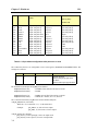
1
RL™
16-bit Controller with 16-bit SRAM & Flash, 100 Base-T Ethernet,
Opto-couplers, RS232/485/422 and 2GB CompactFlash Interface,
Based on the 40MHz Am186ER or 80MHz RDC R1100
Technical Manual
1724 Picasso Avenue, Davis, CA 95616-0547, USA
Tel: 530-758-0180
Fax: 530-758-0181
Email: [email protected]
http://www.tern.com
COPYRIGHT
R-Engine, RL, A-Engine, A-Core86, A-Core, i386-Engine, MemCard-A,
MotionC, and ACTF are trademarks of TERN, Inc.
Am186ER is a trademark of Advanced Micro Devices, Inc.
Paradigm C/C++ is a trademark of Paradigm Systems.
Windows95/98/2000/NT/ME/XP are trademarks of Microsoft Corporation.
Version 1.1
June 3, 2004
No part of this document may be copied or reproduced in any form or by any means
without the prior written consent of TERN, Inc.
© 2002
1724 Picasso Avenue, Davis, CA 95616-0547, USA
Tel: 530-758-0180 Fax: 530-758-0181
Email: [email protected]
http://www.tern.com
Important Notice
TERN is developing complex, high technology integration systems. These systems are
integrated with software and hardware that are not 100% defect free. TERN products are
not designed, intended, authorized, or warranted to be suitable for use in life-support
applications, devices, or systems, or in other critical applications. TERN and the Buyer
agree that TERN will not be liable for incidental or consequential damages arising from
the use of TERN products. It is the Buyer's responsibility to protect life and property
against incidental failure.
TERN reserves the right to make changes and improvements to its products
without providing notice.
RL
Chapter 1: Introduction
Chapter 1: Introduction
1.1 Technical Manual Organization
This technical manual will require special organization to accommodate the possibility of configuring the
RL with two different CPUs. The CPUs are very similar, yet they do have a few differences. For purposes
of organization, it will be assumed that throughout this technical manual, all information given is accurate
for both CPUs, unless otherwise stated. In general, it will be written referring to the Am186ER, but will
implicitly apply to the R1100. When information may deviate between CPUs, it will be explicitly shown.
1.2 Functional Description
The RL™ is a controller designed for industrial machine control applications. This industrial embedded
controller integrates 20 isolated opto-coupler inputs, 35 solenoid drivers, 100 Base-T Ethernet connection,
5 RS232/485/422 serial ports, and CompactFlash mass data storage support on a single PCB. It is ideal for
industrial process control, high speed LAN, or remote communication machine control applications.
The RL utilizes a high performance C/C++ programmable 186-generation CPU (80MHz R1100 or 40 MHz
AM186ER) with a 16-bit external data bus, supporting fast code execution. It has 256KW 16-bit Flash and
256KW 16-bit battery-backed SRAM. Three CPU internal timer/counters can be used to count or time
external events, or to generate non-repetitive or variable duty-cycle waveforms as PWM outputs. A realtime clock (DS1337, Dallas) provides clock/calendar with two time-of-day alarms.
A 50-pin CompactFlash receptacle allows access to mass storage CompactFlash cards (up to 2 GB). TERN
C/C++ programmable software packages with FAT16 file system libraries are available.
An i2Chip™ Fast Ethernet Module can be installed to provide 100M Base-T network connectivity,
allowing the RL to work with high-bandwidth modern Ethernet networks. This Module implements
TCP/IP, UDP, ICMP and ARP with a combination of hardware/software. It has 16KB internal transmit and
receiving buffer which is mapped into host processor’s direct memory. The host can access the buffer via
high speed DMA transfers. The hardware Ethernet module releases internet connectivity and protocol
processing from the host processor. It supports 4 independent stack connections simultaneously at a 4Mbps
protocol processing speed. An RJ45 8-pin connector is on-board for connecting to 10/100 Base-T Ethernet
network.
Five RS232 serial ports are onboard. The CPU’s internal UART is used for remote debugging, but is also
available for user application. Two Dual UARTs (SC26C92) provide 4 more UARTs. All UARTs have
deep FIFOs to minimize receiver overrun and to reduce interrupt overhead. One RS232 port can be
converted to RS485, or RS422.
Five power Darlington array chips (ULN2003A) are installed in five DIP sockets, providing a total of 35
high voltage sinking drivers. Each driver is capable of sinking 350 mA at 50V per line. They can directly
drive solenoids, relays, or lights. In place of the ULN2003As, resistor packs or DAC chips (with
modification) can be optionally installed to provide TTL I/O or up to 10 analog outputs. A total of 20
opto-couplers are on-board to provide isolation for high voltage inputs. Furthermore, some control
applications need to trigger an event under combined conditions of several sensors/switches. As a result,
four of the 20 opto-couplers are routed to an on-board PAL, allowing flexible hardware-configurable input
logic to trigger interrupts. An additional 20 TTL I/O lines are available on the J2 pin header, including bidirectional I/Os from the PPI (82C55) and multifunctional CPU internal PIOs.
1-1
Chapter 1: Introduction
RL
Optional high efficient Switching Regulator (LM2575) provides an external control pin to shutdown 5V
and enter µA standby mode, waking-up on an active-low signal. The RL requires 8.5V to 12V DC power
supply with default linear regulator, or up to 30V DC power input with switching regulator without
generating excessive heat.
1.3 Features
• Dimensions: 4.9 x 3.5 x 0.3 inches
• Temperature: -40°C to +80°C
• 40 MHz, 16-bit CPU (Am186ER), Intel 80x86 compatible, OR
• 80 MHz, 16-bit CPU (R1100)
• 32KB internal RAM, Am186ER ONLY
• Easy to program in C/C++
• Power consumption: 200 mA at 5V
• Standby mode: 50µA
• Power input: + 9V to +12V unregulated DC with default linear regulator
+ 9V to +30V unregulated DC with optional switching regulator
• Up to 256 KW 16-bit SRAM, 256 KW 16-bit Flash
• Up to 2GB CompactFlash with FAT16 File system support
• Flexible hardware-configurable input logic
• Hardware TCP/IP stack for 100 Base-T Ethernet
• Suitable for protected industrial control applications
• 35 Solenoid Drivers, 20 Opto-coupler inputs
• 16-bit external data bus expansion port
• 5 serial ports (1 from Am186ER, four from 2 SCC2692) support full-duplex 7, 8 or 9-bit asynchronous
communication (only SCC2692 supports 9-bit)
• 2 high-speed PWM outputs
• 6 external interrupt inputs, 3 16-bit timer/counters
• 32 multifunctional I/O lines from Am186ER
• 24 bi-directional I/O lines from 82C55 PPI
• 512-byte serial EEPROM
• Supervisor chip (691) for reset and watchdog
• Real-time clock (DS1337), lithium coin battery
1-2
RL
Chapter 1: Introduction
1.4 Physical Description
The physical layout of the RL is shown in Figure 1.1.
Switching
Regulator
SCC2692
Dual UART
Step 2 Jumper
J2 pins 38 & 40
+3.3V Regulator
J2 Header
Interrupts
PIOs
SER0
(debug port)
50-pin CF
socket
+12V Input
Ground
100 Base-T
Ethernet port
20 Optoisolated
inputs
J3 Header
Opto-isolators
J4 Header
HV I/O
PPI
24 bi-directional
TTL level I/Os
Figure 1.1 Physical layout of the RL
1-3
Chapter 1: Introduction
RL
Power On or Reset
Step 2 jumper
set?
YES
NO
STEP 1
ACTF menu sent out through ser0
at 19200 baud
STEP 2
Go to Application Code CS:IP
CS:IP in EEPROM:
0x10=CS high byte
0x11=CS low byte
0x12=IP high byte
0x13=IP low byte
Figure 1.2 Flow chart for ACTF operation
The “ACTF boot loader” resides in the top protected sector of the 256KW on-board Flash chip (29F400).
At power-on or RESET, the “ACTF” will check the STEP 2 jumper. If STEP 2 jumper is not installed, the
ACTF menu will be sent out from serial port0 at 19200 baud. If STEP 2 jumper is installed, the “jump
address” located in the on-board serial EEPROM will be read out and the CPU will jump to that address. A
DEBUG kernel “re40_115.hex” (re80_115.hex when using the 80MHz version) can be downloaded to a
starting address of “0xFA000” of the 256KW on-board flash chip.
There is no ROM socket on the RL. The user’s application program must reside in SRAM for debugging in
STEP1, reside in battery-backed SRAM for the standalone field test in STEP2, and finally be programmed
into Flash for a complete product. For production, the user must produce an ACTF-downloadable HEX file
for the application, based on the DV-P Kit. The “STEP2” jumper (J2 pins 38-40) must be installed for
every production-version board.
Step 1 settings
In order to communicate with the RL with Paradigm C++, the RL must meet these requirements. See next
section “Prepare for Debug Mode”. By default, steps 1-3 are done at the factory.
1) RE40_115.HEX (re80_115.hex with 80MHz version) must be pre-loaded into Flash starting address
0xfa000
2) The on-board EE must have the jump address for the RE40_115.HEX with starting address of 0xfa000.
3) The STEP2 jumper must be installed on J2 pins 38-40.
4) The SRAM installed must be large enough to hold your program.
For a 64 KW SRAM, the physical address is 0x00000-0x01ffff
For a 256 KW SRAM, the physical address is 0x00000-0x07ffff
For further information on programming the RL, refer to the Software chapter.
1-4
RL
Chapter 1: Introduction
1.5 RL Programming Overview
Preparing for Debug Mode
1. Connect RL to PC with RS-232 link at 19,200, N, 8, 1
2. Power on RL with step 2 jumper removed (J2.38, 40)
3. ACTF menu sent to hyper terminal
4..Type ‘D’, <enter>. Send tern\186\rom\re\l_debug.hex
5. Type ‘G04000” to run l_debug.hex
6. Send tern\86\rom\re\re40_115.hex (re80_115.hex with
80MHz version). Starts at 0xFA000
7. Type ‘GFA000’, <enter>. Set Step 2 jumper
(J2.38=J2.40)
8. On-board LED blinks twice, then stays on.
Step 1: Debug Mode
1. Launch Paradigm C/C++
2. Open “rl.ide” in the tern\186\samples\rl directory
3. Run samples.
4. Use samples to build application in C/C++
5. Single step, set breakpoints, debug code
6. Debug kernel must be running each time to download.
7. At power up, if LED does not blink twice then stay on,
repeat steps 1-3 and 7-10 of above section.
Step 2: Standalone Mode
1. Run standalone mode, away from PC. Application resides
in battery-backed SRAM. Set CS:IP to point to application.
2. Power on RL without step 2 jumper set.
3. See menu at hyper terminal. 19,200, N, 8, 1
4. Type ‘G08000’ to jump to and execute code in SRAM
5. Set step 2 jumper, cycle power. Will execute code in
SRAM at every power-up.
6. Test application.
7. Return to Step 1 as necessary
Step 3: Production
1. Generate application HEX file with Paradigm C/C++ based
on field tested source code.
2. Power on board with step 2 jumper removed. See menu at
hyper terminal.
3. Use ‘D’ command to download l_29f40r.hex in the
tern\186\rom\re directory. Will prepare flash.
4. Send application HEX file.
5. Use ‘G’ command to modify CS:IP to point to application in
flash, type ‘G80000’ at menu.
6. Set step 2 jumper.
1-5
Chapter 1: Introduction
RL
1.6 Minimum Requirements for RL System Development
1.6.1 Minimum Hardware Requirements
•
•
•
•
PC or PC-compatible computer with serial COMx port that supports 115,200 baud
RL controller
PC-V25 serial cable (RS-232; DB9 connector for PC COM port and IDE 2x5 connector for controller)
center negative wall transformer (+9V, 500 mA), and power jack adapter (sent with EV-P/DV-P kit)
1.6.2 Minimum Software Requirements
• TERN EV-P Kit installation CD and a PC running: Windows 95/98/NT/ME/2000/XP
With the EV-P Kit, you can program and debug the RL in Step One and Step Two, but you cannot run Step
Three. In order to generate an application Flash file and complete a project, you will need the Development
Kit (DV-P Kit).
1-6
RL
Chapter 2: Installation
Chapter 2: Installation
2.1 Software Installation
Please refer to the Technical manual for the “C/C++ Development Kit and Evaluation Kit for TERN
Embedded Microcontrollers” for information on installing software.
The README.TXT file on the TERN EV-P/DV-P CD-ROM contains important information about the
installation and evaluation of TERN controllers.
2.2 Hardware Installation
Overview
• Connect Debug-serial cable:
For debugging (STEP 1), place IDE connector on SER0 with red
edge of cable at pin 1
• Connect wall transformer:
Connect 9V wall transformer to power and plug into power jack
adapter, which installs into green screw terminal
Hardware installation for the RL consists primarily of connecting it to your PC and to power. As
mentioned above, it requires installing the debug cable onto SER0 and plugging the output of the wall
transformer into the power jack adapter. The following diagram shows the RL with power applied and
connected to the debug cable.
2-1
Chapter 2: Installation
RL
2.2.1 Connecting the RL to power and debug cable
The red edge of the serial cable should align with pin 1 of the 5x2 pin header of SER0. Pin 1 of any header
can be located as the pin closest to the name of the header. In other words, the white characters printed on
the PCB that identify each header indicate pin 1 of that header.
To DB9 connector.
Connect to COM1 of PC.
Output of wall transformer
Use power jack adapter
supplied with EV-P kit
SER0
Red edge of cable aligned
with pin 1 of header
With the connections shown above, the RL is ready to communicate with the PC, either through a hyper
terminal or with Paradigm C/C++.
2-2
RL
Chapter 3: Hardware
Chapter 3: Hardware
3.1 Am186ER AND RDC R1100
The RL is compatible with two different CPUs. Both offer and support the same on-board peripherals as
well as the on the CPU itself, aside from a few differences. The Am186ER, from AMD, uses times-four
crystal frequency, while the R1100, from RDC, uses times-eight. The RL uses a 10MHz system clock,
giving the Am186ER a CPU clock of 40MHz and the R1100 a CPU clock of 80MHz. Both CPUs operate
at +3.3V, with lines +5V tolerant. The RDC 1100 supports the same 80C188 microprocessor instruction
set, but uses an internal RISC core architecture.
3.2 Am186ER – Introduction
The Am186ER is based on the industry-standard x86 architecture. The Am186ER controllers are higherperformance, more integrated versions of the 80C188 microprocessors. In addition, the Am186ER has new
peripherals. The on-chip system interface logic can minimize total system cost. The Am186ER has one
asynchronous serial port, one synchronous serial port, 32 PIOs, a watchdog timer, additional interrupt
pins, DMA to and from serial ports, a 16-bit reset configuration register, and enhanced chip-select
functionality.
In addition, the Am186ER has 32KB of internal volatile RAM. This provides the user with access to high
speed zero wait-state memory. In some instances, users can operate the RL without external SRAM,
relying only on the Am186ER’s internal RAM.
3.3 RDC R1100 – Introduction
The RDC 1100 is based on RISC internal architecture while still supporting the same 80C188
microprocessor instruction set. It provides faster operation than the Am186ER, allowing it to operate at up
to 80MHZ, based a 10MHz system clock and times-eight crystal operation. The RDC R1100 does not offer
internal RAM like the Am186ER, so external SRAM is mandatory if using the RDC R1100.
3.4 Am186ER – Features
Clock
Due to its integrated clock generation circuitry, the Am186ER microcontroller allows the use of a timesfour crystal frequency. The design achieves 40 MHz CPU operation, while using a 10 MHz crystal.
The R1100 offers times-eight crystal frequency, achieving 80MHz operation based on a 10MHz crystal.
The system CLKOUTA signal is routed to J1 pin 4, default 40 MHz. The CLKOUTB signal is not
connected in the RL.
CLKOUTA remains active during reset and bus hold conditions. The RL initial function ae_init(); disables
CLKOUTA and CLKOUTB with clka_en(0); and clkb_en(0);
You may use clka_en(1); to enable CLKOUTA=CLK=J1 pin 4.
Asynchronous Serial Port
The Am186ER and R1100 CPU has one asynchronous serial channel. It support the following:
3-1
Chapter 3: Hardware
RL
• Full-duplex operation
• 7-bit, and 8-bit data transfers
• Odd, even, and no parity
• One or two stop bits
• Error detection
• Hardware flow control
• DMA transfers to and from serial port (Am186ER ONLY)
• Transmit and receive interrupts
• Maximum baud rate of 1/16 of the CPU clock speed
• Independent baud rate generators
The software drivers for the asynch. serial port implement a ring-buffered DMA receiving and ringbuffered interrupt transmitting arrangement. See the sample file tern\186\samples\ae\s0_echo.c
An external SCC26C92 UART is located in position U4 and U10. For more information about the external
UART SCC26C92, please refer to the section in this manual on the SCC26C92.
Timer Control Unit
The timer/counter unit has three 16-bit programmable timers: Timer0, Timer1, and Timer2.
Timer0 and Timer1 are connected to four external pins:
Timer0 output = P10 = J2 pin 12
Timer0 input
= P11 = J2 pin 14
Timer1 output = P1
= J2 pin 29
Timer1 input
= P0
= J2 pin 20
These two timers can be used to count or time external events, or they can generate non-repetitive or
variable-duty-cycle waveforms.
Timer2 is not connected to any external pin. It can be used as an internal timer for real-time coding or
time-delay applications. It can also prescale timer 0 and timer 1 or be used as a DMA request source.
The maximum rate at which each timer can operate is 10 MHz. Timer inputs take up to six clock cycles to
respond to clock or gate events. See the sample programs timer0.c and ae_cnt0.c in the \samples\ae
directory.
PWM outputs
The Timer0 and Timer1 outputs can also be used to generate non-repetitive or variable-duty-cycle
waveforms. The timer output takes up to 6 clock cycles to respond to the clock input. Thus the minimum
timer output cycle is 25 ns x 6 = 150 ns.
Each timer has a maximum count register that defines the maximum value the timer will reach. Both
Timer0 and Timer1 have secondary maximum count registers for variable duty cycle output. Using both
the primary and secondary maximum count registers lets the timer alternate between two maximum values.
MAX. COUNT A
MAX. COUNT B
3-2
RL
Chapter 3: Hardware
Power-save Mode
The RL is an ideal core module for low power consumption applications. The power-save mode of the
Am186ER reduces power consumption and heat dissipation, thereby extending battery life in portable
systems. In power-save mode, operation of the CPU and internal peripherals continues at a slower clock
frequency. When an interrupt occurs, it automatically returns to its normal operating frequency.
The DS1337 on the RL has a VOFF signal routed to H1 pin 1. VOFF is controlled by the battery-backed
DS1337. The VOFF signal can be programmed by software to be in tri-state or to be active low. The
DS1337 can be programmed in interrupt mode to drive the VOFF pin at 1 second, 1 minute, or 1 hour
intervals. With the Switching Regulator installed (optional), the user can use VOFF to release VOFF and
shut down the on-board switching regulator. By default, the VOFF option is disabled by tying VOFF to
Ground. The user can also use the VOFF line to control an external switching power supply that turns the
power supply on/off.
3.5 Am186ER PIO lines
The Am186ER has 32 pins available as user-programmable I/O lines. Each of these pins can be used as a
user-programmable input or output signal, if the normal shared function is not needed. A PIO line can be
configured to operate as an input or output with or without a weak pull-up or pull-down, or as an opendrain output. A pin’s behavior, either pull-up or pull-down, is pre-determined and shown in the table
below.
After power-on/reset, PIO pins default to various configurations. The initialization routine provided by
TERN libraries reconfigures some of these pins as needed for specific on-board usage, as well. These
configurations, as well as the processor-internal peripheral usage configurations, are listed below in Table
3.1.
PIO
Function
Power-On/Reset
status
RL Pin No.
RL Initial
after ae_init();
function call
P0
P1
P2
P3
P4
P5
P6
P7
P8
P9
P10
P11
P12
P13
P14
P15
P16
P17
Timer1 in
Timer1 out
/PCS6/A2
/PCS5/A1
DT/R
/DEN/DS
SRDY
A17
A18
A19
Timer0 out
Timer0 in
DRQ0
DRQ1
/MCS0
/MCS1
/PCS0
/PCS1
Input with pull-up
Input with pull-down
Input with pull-up
Input with pull-up
Normal
Normal
Normal
Normal
Normal
Normal
Input with pull-down
Input with pull-up
Input with pull-up
Input with pull-up
Input with pull-up
Input with pull-up
Input with pull-up
Input with pull-up
J2 pin 20
J2 pin 29
J2 pin 27
U4 pin 39
J2 pin 38
J2 pin 30
J2 pin 35
N/A
N/A
J2 pin 25
J2 pin 12
J2 pin 14
J1 pin 26
J2 pin 11
JP1 pin 2
J2 pin 23
J1 pin 19
N/A
Input with pull-up
Input with pull-up
PAL
SCC2692 select
Input with pull-up Step 2
Input
Input
A17
A18
A19
Input with pull-down
Input with pull-up
Output
Input with pull-up
Input with pull-up
Input with pull-up
/PCS0
/PCS1
3-3
Chapter 3: Hardware
PIO
Function
RL
Power-On/Reset
status
RL Pin No.
RL Initial
after ae_init();
function call
P18
P19
P20
P21
P22
P23
P24
P25
P26
P27
P28
P29
P30
P31
/PCS2
/PCS3
SCLK
SDATA
SDEN0
SDEN1
/MCS2
/MCS3
UZI
TxD
RxD
S6/CLKSEL1
INT4
INT2
Input with pull-up
Input with pull-up
Input with pull-up
Input with pull-up
Input with pull-down
Input with pull-down
Input with pull-up
Input with pull-up
Input with pull-up
Input with pull-up
Input with pull-up
Input with pull-up
Input with pull-up
Input with pull-up
J2 pin 13
J2 pin 31
J2 pin 5
J2 pin 3
N/A
J2 pin 9
J2 pin 17
J2 pin 18
J2 pin 4
J2 pin 34
J2 pin 32
J9 pin 2
U9 pin 14
U9 pin 16
Input with pull-up
Input with pull-up
Input with pull-up
Input with pull-up
Output
Input with pull-up
Input with pull-up
Input with pull-up
Input with pull-up*
TxD0
RxD0
Input with pull-up*
Input with pull-up
Input with pull-up
* Note: P6, P26 and P29 must NOT be forced low during power-on or reset.
Table 3.1 I/O pin default configuration after power-on or reset
The 32 PIO lines, P0-P31, are configurable via two 16-bit registers, PIOMODE and PIODIRECTION. The
settings are as follows:
MODE
0
1
2
3
PIOMODE reg.
0
0
1
1
PIODIRECTION reg.
0
1
0
1
PIN FUNCTION
Normal operation
INPUT with pull-up/pull-down
OUTPUT
INPUT without pull-up/pull-down
RL initialization on PIO pins in ae_init() is listed below:
outport(0xff78,0xc7bc);
// PIODIR1, TxD, RxD, P16=PCS0, P17=PCS1
outport(0xff76,0x2040);
// PIOM1
outport(0xff72,0xec73);
// PDIR0, P12=OUTPUT, P2=PCS6, P3=PCS5
outport(0xff70,0x1040);
// PIOM0, P6 = INPUT, P7=A17, P8=A18
The C function in the library re_lib can be used to initialize PIO pins.
void pio_init(char bit, char mode);
Where bit = 0-31 and mode = 0-3, see the table above.
Example:
pio_init(10, 2); will set P10 as output
pio_init(1, 0); will set P1 as Timer1 output
void pio_wr(char bit, char dat);
pio_wr(10,1); set P10 pin high, if P10 is in output mode
pio_wr(10,0); set P12 pin low, if P10 is in output mode
3-4
RL
Chapter 3: Hardware
unsigned int pio_rd(char port);
pio_rd (0); return 16-bit status of P0-P15, if corresponding pin is in input mode,
pio_rd (1); return 16-bit status of P16-P31, if corresponding pin is in input mode,
Some of the I/O lines are used by the RL system for on-board components (Table 3.2). We suggest that
you not use these lines unless you are sure that you are not interfering with the operation of such
components (i.e., if the component is not installed).
Signal
P2
P3
P4
P7
P8
P14
P17
P22
P27
P28
P29
/INT0
/INT3
/INT4
Pin
/PCS6
/PCS5
/DT
A17
A18
/MCS0
/PCS1
SDEN0
TxD
RxD
S6
U4.24
U10.24
JP1.2
Function
Clock input for U9 PAL
Chip select for U4 SC26C92
Step Two jumper
Never use for application
Never use for application
Chip select for Ethernet module
Chip Select for U18 decoder
Synchronous serial interface for RTC, EEPROM
TxD0
RxD0
Reserved for EEPROM, LED, RTC, and Watchdog timer
U4 SC26C92 UART interrupt.
U10 SC26C92 UART interrupt
Interrupt for Ethernet module
Table 3.2 I/O lines used for on-board components
3.6 I/O Mapped Devices
I/O Space
External I/O devices can use I/O mapping for access. You can access such I/O devices with inportb(port)
or outportb(port,dat). These functions will transfer one byte or word of data to the specified I/O address.
The external I/O space is 64K, ranging from 0x0000 to 0xffff.
The default I/O access time is 15 wait states. You may use the function void io_wait(char wait) to define
the I/O wait states from 0 to 15. The system clock is 100 ns for both CPUs, while the CPU clock is 25ns
for the Am186ER and 12.5ns for the R1100. Details regarding this can be found in the Software chapter,
and in the Am186ER User’s Manual. Slower components, such as most LCD interfaces, might find the
maximum programmable wait state of 15 cycles still insufficient. Due to the high bus speed of the system,
some components need to be attached to I/O pins directly.
For details regarding the chip select unit, please see Chapter 5 of the Am186ER User’s Manual.
The table below shows more information about I/O mapping.
I/O space
Select
Location
Usage
0x0000-0x00ff
0x0100-0x01ff
0x0200-0x02ff
0x0300-0x03ff
/PCS0
/PCS1
/PCS2
/PCS3
J1 pin 19=P16
U18.4
J2 pin 13=P18
J2 pin 31=P19
USER*
U18 decoder
USER
USER
3-5
Chapter 3: Hardware
0x0400-0x04ff
0x0500-0x05ff
0x0600-0x06ff
RL
/PCS4
/PCS5
/PCS6
J2 pin 15=P3
U9.1
Reserved
SC26C92
PAL
*PCS0 may be used for other TERN peripheral boards, such as UR8, P100, etc.
To illustrate how to interface the RL with external I/O boards, a simple decoding circuit for interfacing to
an 82C55 parallel I/O chip is shown in Figure 3.1.
82C55
74HC138
RST
P00-P07
Y0 15 NC
A5
1
A
A0
Y1 14 /SEL20
A6
2
A1
B
Y2 13 /SEL40
A7
3
C
Y3 12 /SEL60
P10-P17
/SEL20 /CS
Y4 11 /SEL80
/WR
/WR
Y5 10 /SELA0
G2A
4
/PCS0
Y6 9 /SELC0
G2B
5
/RD
/RD
VCC 6
Y7 7 /SELF0
G1
P20-P27
D0-D7
Figure 3.1 Interface the RL to external I/O devices
The function ae_init() by default initializes the /PCS0 line at base I/O address starting at 0x00. You
can read from the 82C55 with inportb(0x020) or write to the 82C55 with outportb(0x020,dat). The call to
inportb(0x020) will activate /PCS0, as well as putting the address 0x00 over the address bus. The decoder
will select the 82C55 based on address lines A5-7, and the data bus will be used to read the appropriate
data from the off-board component.
Programmable Peripheral Interface (82C55A)
U5 PPI (82C55) is a low-power CMOS programmable parallel interface unit for use in microcomputer
systems. It provides 24 I/O pins that may be individually programmed in two groups of 12 and used in
three major modes of operation.
In MODE 0, the two groups of 12 pins can be programmed in sets of 4 and 8 pins to be inputs or outputs.
In MODE 1, each of the two groups of 12 pins can be programmed to have 8 lines of input or output. Of
the 4 remaining pins, 3 are used for handshaking and interrupt control signals. MODE 2 is a strobed bidirectional bus configuration. See data sheet for details on different mode: tern_docs\parts\82c55a.pdf.
3-6
RL
Chapter 3: Hardware
7
6
5
4
3
2
1
0
GROUP 1
P o rt 2
(L o w e r)
P o rt 1
M ode
0
O u tp u t
1
In p u t
0
O u tp u t
1
In p u t
0
M ode 0
1
M ode 1
GROUP 2
P o rt 2
(U p p e r)
P o rt 0
M ode
C om m and
S e le c t
0
1
0
O u tp u t
1
In p u t
0
O u tp u t
1
In p u t
00
M ode 0
01
M ode 1
1X
M ode 2
B it
m a n ip u la tio n
M ode
S e le c t
Figure 3.2 Mode Select Command Word
The RL maps U5, the 82C55/uPD71055, at base I/O address 0x1A0.
The ports/registers are offsets of this I/O base address.
The command register = 0x1A6; Port 0 = 0x1A0; Port 1 = 0x1A2; Port 2 = 0x1A4.
The following code example will set all ports to output mode:
outportb(0x1A6,0x80);
// mode 0 output, all pins
outportb(0x1A0,0x55);
// Port 0, alternating high/low on pins
outportb(0x1A2,0x55);
// Port 1, alternating high/low on pins
outportb(0x1A4,0x55);
// Port 2, alternating high/low on pins
To set all ports to input mode:
outportb(0x1A6, 0x9b);
// mode 0 input, all pins
3-7
Chapter 3: Hardware
RL
You can read the ports with:
inportb(0x1A0); // port 0
inportb(0x1A2); // port 1
inportb(0x1A4); // port 2
This returns an 8-bit value for each port, with each bit corresponding to the appropriate line on the port,
where the most significant bit refers to Ix7 and the least significant bit refers to Ix0.
All PPI lines are routed to high voltage drivers at U11, U12, and U13, with the corresponding high voltage
outputs routed to J4. See section on high voltage drivers for alternate configurations. I27 – I24 are routed
to the J2 pin header.
Real-time Clock DS1337
The DS1337 serial real-time clock is a low-power clock/calendar with two programmable time-of-day
alarms and a programmable square-wave output. Address and data are transferred serially via a 2-wire,
bidirectional bus. The clock/calendar provides seconds, minutes, hours, day, date, month, and year
information. The data at the end of the month is automatically adjusted for months with fewer than 31
days, including corrections for leap year. The clock operates in either 24-hour or 12-hour format with
AM/PM indicator.
The RTC is accessed via software drivers rtc_init() and rtc_rds(). Refer to sample code in the
tern\186\samples\re directory for re_rtc.c. See tern\186\samples\rl\rl.ide.
It is also possible to configure the real-time clock to raise an output line attached to an external interrupt, at
1/64 second, 1 second, 1 minute, or 1 hour intervals. This can be used in a time-driven application, or the
VOFF signal can be used to turn on/off the controller using an external switching power supply.
UART SC26C92
Two dual UARTs (SC26C92, Phillips, U4 and U10) are installed on the RL, providing 4 UARTs. Each
SC26C92 includes two independent full-duplex asynchronous receiver/transmitters, a quadruple buffered
receiver data register, an interrupt control mechanism, programmable data format, selectable baud rate for
the receiver and transmitter, a multi-functional and programmable 16-bit counter/timer, an on-chip crystal
oscillator, and a multi-purpose input/output including RTS and CTS mechanism.
A 3.6864 MHz external crystal is installed as the default crystal for the dual UARTs.
By default, all UARTs are configured with RS-232 drivers. One port can be optionally configured to
RS-485 or RS-422.
For more detailed information, refer to the SC26C92 data sheets (Phillips Semiconductors) or on the CD in
the tern_docs\parts directory.
Sample programs for the SC26C92 can be found in the c:\tern\186\samples\rl directory. See
tern\186\samples\rl\rl.ide.
3.7 Other Devices
A number of other devices are also available on the RL. Some of these are optional, and might not be
installed on the particular controller you are using. For a discussion regarding the software interface for
these components, please see the Software chapter.
3-8
RL
Chapter 3: Hardware
On-board Supervisor with Watchdog Timer
The MAX691/LTC691 (U6) is a supervisor chip. With it installed, the RL has several functions: watchdog
timer, battery backup, power-on-reset delay, power-supply monitoring, and power-failure warning. These
will significantly improve system reliability.
Watchdog Timer
The watchdog timer is activated by setting a jumper on J9 of the RL. The watchdog timer provides a
means of verifying proper software execution. In the user's application program, calls to the function
hitwd() (a routine that toggles the P29 = WDI pin of the MAX691) should be arranged such that the WDI
pin is accessed at least once every 1.6 seconds. If the J9 jumper is on and the WDI pin is not accessed
within this time-out period, the watchdog timer pulls the WDO pin low, which asserts /RESET. This
automatic assertion of /RESET may recover the application program if something is wrong. After the RL is
reset, the WDO remains low until a transition occurs at the WDI pin of the MAX691. When controllers are
shipped from the factory the J9 jumper is off, which disables the watchdog timer.
The Am186ER has an internal watchdog timer. This is disabled by default with ae_init().
Battery Backup Protection
The backup battery protection protects data stored in the SRAM and RTC. The battery-switch-over circuit
compares VCC to VBAT (+3 V lithium battery positive pin), and connects whichever is higher to the
VRAM (power for SRAM and RTC). Thus, the SRAM and the real-time clock DS1337 are backed up. In
normal use, the lithium battery should last about 3-5 years without external power being supplied. When
the external power is on, the battery-switch-over circuit will select the VCC to connect to the VRAM.
EEPROM
A serial EEPROM of 512 bytes (24C04) is be installed in U7. The RL uses the P22 and P29 to interface
with the EEPROM. The EEPROM can be used to store important data such as a node address, calibration
coefficients, and configuration codes. It typically has 1,000,000 erase/write cycles. The data retention is
more than 40 years. EEPROM can be read and written by simply calling the functions ee_rd() and
ee_wr().
A range of lower addresses in the EEPROM is reserved for TERN use, 0x00 – 0x1F. The addresses 0x20
to 0x1FF are for user application.
Opto-couplers
The RL supports 20 opto-couplers in 5 PS2501-4 packages. These opto-couplers can be used for digital
inputs, relay contact monitoring, or powerline monitoring. Each opto-coupler has a 3µs ON time and 5µs
OFF time. The status of the opto-couplers is read via the input ports of the SC26C92s and CPU PIOs, 14
from the two SC26C92s and 2 from PIO lines. All inputs to the opto-couplers are routed to the J3 header.
The user is required to provide supply voltage to the opto-couplers. The RL is shipped from the factory
with the supply voltage tied to +12VI via jumper on the J3 header. The output lines of the opto-couplers
(IS0-IS6, IP0-IP6, P11, and P0) are pulled high via 10K ohm resistor network making the opto-coupler
OFF by default. Pulling input lines low will turn the opto-coupler ON and pull output lines low. See
sample project: c:\tern\186\samples\rl\rl.ide for example program (rl_opto.c).
3-9
Chapter 3: Hardware
RL
High Voltage, High-current drivers
The ULN2003 has high voltage, high current Darlington transistor arrays, consisting of seven silicon NPN
Darlington pairs on a common monolithic substrate. There are five ULN2003s on the RL in locations U11U15, providing a total of 35 channels. All channels feature open-collector outputs for sinking 350 mA at
50V, and integral protection diodes for driving inductive loads. Peak inrush currents of up to 500 mA
sinking are allowed. These outputs may be paralleled to achieve high-load capability, although each driver
has a maximum continuous collector current rating of 350 mA at 50V. The maximum power dissipation
allowed is 2.20 W per chip at 25 degrees C (°C). The common substrate G is tied to ground by default. For
inductive loads, K (J3 pin 39) connects to the protection diodes in the ULN2003 chips and should be tied
to highest voltage in the external load system. K can be connected to a user provided voltage at J3 pin 40.
ULN2003 is a sinking driver, not a sourcing driver. An example of typical application wiring is shown
in 0.
O1
Solenoid
+12V
Power Supply
GND/SUB
ULN2003 TinyDrive
K
+12V
GND/SUB
Figure 3.3 Drive inductive loads with high voltage/current drivers.
By design, the sockets at locations U11- U15 only allow sinking drivers. Sourcing drivers are not allowed.
However, if TTL level I/Os are needed, the ULN2003s can be replaced by resistor pack ICs. U11 – U13
are accessed by the U5 PPI (82C55), and with resistor packs installed, can provide user programmable TTL
level inputs and/or outputs. Locations U14 and U15 are accessed via the output ports of the SC26C92s, and
with resistor packs installed can provide only TTL level outputs.
Ethernet Module
The RL supports an i2Chip W3100A which is an LSI of hardware protocol stack that provides an easy,
low-cost solution for high-speed internet connectivity for digital devices by allowing simple installation of
TCP/IP stack in the hardware. The i2Chip offers a quick and easy way to add Ethernet networking
functionality to embedded controllers. It can completely offload internet connectivity and processing
standard protocols from the host system, reducing development time and cost. It contains TCP/IP protocol
stacks such as TCP, UDP, IP, ARP and ICMP protocols, as well as Ethernet protocols such as Data Link
Control and MAC protocol. The full datasheet is provided on the TERN CD:
\tern_docs\parts\w3100a datasheet 3.1.pdf. Also find sample programs for accessing the module in the
3-10
RL
Chapter 3: Hardware
RL sample project, c:\tern\186\sampels\rl\rl.ide. Sample programs include i2chip.c and i2_dma.c. The
module is accessed by P14 = /MCS0 (midrange chip select). The chip select can be mapped into memory
by initializing the MMCS and MPCS registers. See chapter 5 of the Am186ER technical manual
(amd_docs\am186er).
3.8 Headers and Connectors
Expansion Headers J1 and J2
There are two 20x2 0.1 spacing headers for RL expansion. Most signals are directly routed to the
Am186ER processor.
These signals are +3.3V signals, but are +5V tolerant. Any
voltages above +5V will certainly damage the board.
J2 Signal
GND
P4
TxD0
RxD0
P5
TxDA
RxDA
I25
P0
P25
I27
P11
P10
/INT0
/INT1
P26
GND
40
38
36
34
32
30
28
26
24
22
20
18
16
14
12
10
8
6
4
2
39
37
35
33
31
29
27
25
23
21
19
17
15
13
11
9
7
5
3
1
J1 Signal
VCC
P14
P6
P19
P1
P2
A19
P15
I24
P24
I26
P18
P13
P23
NMI
SCLK
SDAT
VCC
/BHE
D15
/RST
RST
P16
D14
D13
D12
/WR
/RD
D11
D10
D9
D8
1
3
5
7
9
11
13
15
17
19
21
23
25
27
29
31
33
35
37
39
2
4
6
8
10
12
14
16
18
20
22
24
26
28
30
32
34
36
38
40
GND
CLK
GND
D0
D1
D2
D3
D4
D5
D6
D7
GND
P12
A7
A6
A5
A4
A3
A2
A1
Table 3.3 Signals for J2 and J1, 20x2 expansion ports
3-11
RL
Chapter 4: Software
Chapter 4: Software
Please refer to the Technical Manual of the “C/C++ Development Kit for TERN 16-bit Embedded
Microcontrollers” for details on debugging and programming tools.
An IDE project for the RL has been pre-built for your convenience. It is located in the
\tern\186\samples\rl directory. The filename is “rl.ide”. It includes sample code linked to the correct
libraries, ready to run and access RL hardware.
Guidelines, awareness, and problems in an interrupt driven environment
Although the C/C++ Development Kit provides a simple, low cost solution to application engineers, some
guidelines must be followed. If they are not followed, you may experience system crashes, PC hang-ups,
and other problems.
The debugging of interrupt handlers with the Remote Debugger can be a challenge. It is possible to debug
an interrupt handler, but there is a risk of experiencing problems. Most problems occur in multi-interruptdriven situations. Because the remote kernel running on the controller is interrupt-driven, it demands
interrupt services from the CPU. If an application program enables interrupt and occupies the interrupt
controller for longer than the remote debugger can accept, the debugger will time-out. As a result, your PC
may hang-up. In extreme cases, a power reset may be required to restart your PC.
For your reference, be aware that our system is remote kernel interrupt-driven for debugging.
The run-time environment on TERN controllers consists of an I/O address space and a memory address
space. I/O address space ranges from 0x0000 to 0xffff, or 64 KB. Memory address space ranges from
0x00000 to 0xfffff in real-mode, or 1 MB. These are accessed differently, and not all addresses can be
translated and handled correctly by hardware. I/O and memory mappings are done in software to define
how translations are implemented by the hardware. Implicit accesses to I/O and memory address space
occur throughout your program from TERN libraries as well as simple memory accesses to either code or
global and stack data. You can, however, explicitly access any address in I/O or memory space, and you
will probably need to do so in order to access processor registers and on-board peripheral components
(which often reside in I/O space) or non-mapped memory.
This is done with four different sets of similar functions, described below.
poke/pokeb
Arguments: unsigned int segment, unsigned int offset, unsigned int/unsigned char data
Return value: none
These standard C functions are used to place specified data at any memory space location. The segment
argument is left shifted by four and added to the offset argument to indicate the 20-bit address within
memory space. poke is used for writing 16 bits at a time, and pokeb is used for writing 8 bits.
The process of placing data into memory space means that the appropriate address and data are placed on
the address and data-bus, and any memory-space mappings in place for this particular range of memory
will be used to activate appropriate chip-select lines and the corresponding hardware component
responsible for handling this data.
peek/peekb
Arguments: unsigned int segment, unsigned int offset
Return value: unsigned int/unsigned char data
4-1
Chapter 4: Software
RL
These functions retrieve the data for a specified address in memory space. Once again, the segment
address is shifted left by four bits and added to the offset to find the 20-bit address. This address is then
output over the address bus, and the hardware component mapped to that address should return either an
8-bit or 16-bit value over the data bus. If there is no component mapped to that address, this function will
return random garbage values every time you try to peek into that address.
outport/outportb
Arguments: unsigned int address, unsigned int/unsigned char data
Return value: none
This function is used to place the data into the appropriate address in I/O space. It is used most often
when working with processor registers that are mapped into I/O space and must be accessed using either
one of these functions. This is also the function used in most cases when dealing with user-configured
peripheral components.
When dealing with processor registers, be sure to use the correct function. Use outport if you are dealing
with a 16-bit register.
inport/inportb
Arguments: unsigned int address
Return value: unsigned int/unsigned char data
This function can be used to retrieve data from components in I/O space. You will find that most hardware
options added to TERN controllers are mapped into I/O space, since memory space is valuable and is
reserved for uses related to the code and data. Using I/O mappings, the address is output over the address
bus, and the returned 16 or 8-bit value is the return value.
For a further discussion of I/O and memory mappings, please refer to the Hardware chapter of this
technical manual.
4.1 Programming Overview
The ACTF loader in the RL 256KW Flash will perform the system initialization and prepare for new
application code download or immediately run the pre-loaded code. A remote debugger kernel can be
loaded into the Flash located starting 0xfa000. Debugging at baud rate of 115,200 (re40_115.HEX for the
Am186ER and re80_115.HEX for the R1100) is available. A loader file “l_debug.hex” and both debugger
files re40_115.hex and re80_115.HEX, are included in the EV-P/DV-P CD under the
c:\tern\186\rom\re\ directory.
A functional diagram of the ACTF (embedded in the RL) is shown below:
4-2
RL
Chapter 4: Software
Power on or Reset
STEP2 Jumper on ?
J2 pin 38=P4=GND ?
Yes
Read EE for the jump address CS:IP
No
SEND out MENU over SER0 at 19200, N, 8, 1 to
Hyperterminal of Windows95/98
Text command or download new codes
Process Commands
See ACTF-kit and Functions for detail
RUN the program starting at the CS:IP
The C function prototypes supporting Am186ER hardware can be found in header file “ae.h”, in the
c:\tern\186\include directory.
Sample programs can be found in the c:\tern\186\samples\ae, c:\tern\186\samples\re
and c:\tern\186\samples\rl directories.
There is no ROM socket on the RL. The user’s application program must reside in SRAM for debugging in
STEP1, reside in battery-backed SRAM for the standalone field test in STEP2, and finally be programmed
into Flash for a complete product.
The on-board Flash 29F400BT has 256K words of 16-bits each. It is divided into 11 sectors, comprised of
one 16KB, two 8KB, one 32KB, and seven 64KB sectors. The top one 16KB sector is pre-loaded with
ACTF boot strip, the one 8KB sector starting 0xfa000 is for loading remote debugger kernel, and the reset
all sectors are free for application use.
The top 16KB ACTF boot strip is protected.
Two utility HEX files, “l_debug.HEX” and “L_29F40R.HEX”, are designed for downloading into SRAM
starting at 0x04000 with ACTF-PC-HyperTerminal. Use the “D” command to download, and use the “G”
command to run.
“L_DEBUG.HEX” will erase the 8KB sector and load a “re40_115.HEX” or “re80_115.HEX”.
“L_29F40R.HEX” will erase the remaining sectors for downloading your application HEX file.
4-3
Chapter 4: Software
RL
ACTF
Utility
0xFFFFF
0xFC000
Flash
Debug
Kernel
re40_115
0xFA000
0x80000
0x20000
512K SRAM
128K SRAM
0x08000
Beginning of
application in
STEP 1& 2
0x00000
For production, the user must produce an ACTF-downloadable HEX file for the application, based on the
DV-P. The application HEX file can be loaded into the on-board Flash starting address at 0x80000 or
0xC0000. The on-board EE must be modified with a “G80000” or “GC0000” command while in the
ACTF-PC-HyperTerminal Environment.
The “STEP2” jumper (J2 pins 38-40) must be installed for every production-version board.
All files needed to erase/write flash and debug kernels are found in the c:\tern\186\rom\re directory.
Step 1 settings
In order to correctly download a program in STEP1 with Paradigm C/C++, the RL must meet these
requirements:
1) re40_115.hex must be pre-loaded into Flash starting address 0xfa000 (re80_115.hex for 80MHz
version)
2) The SRAM installed must be large enough to hold your program.
For a 128K SRAM, the physical address is 0x00000-0x01ffff
For a 512K SRAM, the physical address is 0x00000-0x07ffff
3) The on-board EE must have a correct jump address for the re40_115.HEX with starting address of
0xfa000.
4) The STEP2 jumper must be installed on J2 pins 38-40.
4-4
RL
Chapter 4: Software
4.2 RE.LIB
RE.LIB is a C library for basic RL operations. It includes the following modules: AE.OBJ, SER0.OBJ,
SER1R.OBJ, and AEEE.OBJ. You need to link RE.LIB in your applications and include the corresponding
header files in your source code. The following is a list of the header files:
Include-file name
Description
AE.H
SER0.H
SER1R.H
AEEE.H
PPI, timer/counter, RTC, Watchdog
Internal serial port 0
External UART SCC26C92
on-board EEPROM
4.3 Functions in AE.OBJ
4.3.1 RL Initialization
ae_init
This function should be called at the beginning of every program running on RL core controllers. It
provides default initialization and configuration of the various I/O pins, interrupt vectors, sets up expanded
DOS I/O, and provides other processor-specific updates needed at the beginning of every program.
There are certain default pin modes and interrupt settings you might wish to change. With that in mind, the
basic effects of ae_init are described below. For details regarding register use, you will want to refer to the
AMD Am186ER Microcontroller User’s manual.
•
Initialize the upper chip select to support the default ROM. The CPU registers are configured such
that:
−
Address space for the ROM is from 0x80000-0xfffff (to map MemCard I/O window)
−
512K ROM Block size operation.
−
Three wait state operation. For details, see the UMCS (Upper Memory Chip Select Register)
reference in the processor User’s manual.
outport(0xffa0, 0x80bf); // UMCS, 512K ROM, 0x80000-0xfffff
•
Initialize LCS (Lower Chip Select) for use with the SRAM. It is configured so that:
−
Address space starts 0x00000, with a maximum of 512K RAM.
−
Three wait state operation. Reducing this value can improve performance.
−
Disables PSRAM, and disables need for external ready.
outport(0xffa2, 0x7fbf); // LMCS, base Mem address 0x0000
•
Initialize MMCS and MPCS so that MCS0 and PCS0-PCS6 (except for PCS4) are configured so:
−
MCS0 is mapped also to a 256K window at 0x80000. If used with MemCard, this
chip select line is used for the I/O window.
−
Sets up PCS5-6 lines as chip-select lines, with three wait state operation.
outport(0xffa8, 0xa0bf); // s8, 3 wait states
outport(0xffa6, 0x81ff); // CS0MSKH
•
Initialize PACS so that PCS0-PCS3 are configured so that:
−
Sets up PCS0-3 lines as chip-select lines, with fifteen wait state operation.
−
The chip select lines starts at I/O address 0x0000, with each successive chip select line
addressed 0x100 higher in I/O space.
4-5
Chapter 4: Software
RL
outport(0xffa4, 0x007f); // CS0MSKL, 512K, enable CS0 for RAM
•
Configure the two PIO ports for default operation. All pins are set up as default input, except for
P29 (used for driving the LED), and peripheral function pins for SER0, as well as chip selects for
the PPI.
outport(0xff78,0xe73c);
// PDIR1, TxD0, RxD0
// P16=PCS0, P17=PCS1
outport(0xff76,0x0000);
// PIOM1
outport(0xff72,0xec7b);
// PDIR0, P12 Output,A18,A17,P2=PCS6
outport(0xff70,0x1000);
// PIOM0, P3 = /PCS5
The chip select lines are set to 15 wait states, by default. This makes it possible to interface with many
slower external peripheral components. If you require faster I/O access, you can modify this number down
as needed. Some TERN components, such as the Real-Time-Clock, might fail if the wait state is decreased
too dramatically. A function is provided for this purpose.
void io_wait
Arguments: char wait
Return value: none.
This function sets the current wait state depending on the argument wait.
wait=0,
wait=1,
wait=2,
wait=3,
wait=4,
wait=5,
wait=6,
wait=7,
wait
wait
wait
wait
wait
wait
wait
wait
states
states
states
states
states
states
states
states
=
=
=
=
=
=
=
=
0, I/O enable for 100 ns
1, I/O enable for 100+25 ns
2, I/O enable for 100+50 ns
3, I/O enable for 100+75 ns
5, I/O enable for 100+125 ns
7, I/O enable for 100+175 ns
9, I/O enable for 100+225 ns
15, I/O enable for 100+375 ns
4.3.2 External Interrupt Initialization
There are up to six external interrupt sources on the RL, consisting of five maskable interrupt pins (INT4INT0) and one non-maskable interrupt (NMI). There are also an additional eight internal interrupt sources
not connected to the external pins, consisting of three timers, two DMA channels, both asynchronous serial
ports, and the NMI from the watchdog timer. For a detailed discussion involving the ICUs, the user should
refer to Chapter 7 of the AMD Am186ER Microcontroller User’s Manual. Or the R1100 user’s manual,
both available on the CD under the amd_docs directory.
Some interrupt lines on the RL are reserved for system use. These include /INT0, INT3 and /INT4.
TERN provides functions to enable/disable all of the 6 external interrupts. The user can call any of the
interrupt init functions listed below for this purpose. The first argument indicates whether the particular
interrupt should be enabled, and the second is a function pointer to an appropriate interrupt service routine
that should be used to handle the interrupt. The TERN libraries will set up the interrupt vectors correctly
for the specified external interrupt line.
At the end of interrupt handlers, the appropriate in-service bit for the IR signal currently being handled
must be cleared. This can be done using the Nonspecific EOI command. At initialization time, interrupt
priority was placed in Fully Nested mode. This means the current highest priority interrupt will be handled
first, and a higher priority interrupt will interrupt any current interrupt handlers. So, if the user chooses to
clear the in-service bit for the interrupt currently being handled, the interrupt service routine just needs to
issue the nonspecific EOI command to clear the current highest priority IR.
To send the nonspecific EOI command, you need to write the EOI register word with 0x8000.
outport(0xff22, 0x8000);
4-6
RL
Chapter 4: Software
void intx_init
Arguments: unsigned char i, void interrupt far(* intx_isr) () )
Return value: none
These functions can be used to initialize any one of the external interrupt channels (for pin locations and
other physical hardware details, see the Hardware chapter). The first argument i indicates whether this
particular interrupt should be enabled or disabled. The second argument is a function pointer, which will
act as the interrupt service routine. The overhead on the interrupt service routine, when executed, is about
20 µs.
By default, the interrupts are all disabled after initialization. To disable them again, you can repeat the call
but pass in 0 as the first argument.
The NMI (Non-Maskable Interrupt) is special in that it can not be masked (disabled). The default ISR will
return on interrupt.
void
void
void
void
void
void
int0_init( unsigned char i,
int1_init( unsigned char i,
int2_init( unsigned char i,
int3_init( unsigned char i,
int4_init( unsigned char i,
nmi_init(void interrupt far
void interrupt far(*
void interrupt far(*
void interrupt far(*
void interrupt far(*
void interrupt far(*
(* nmi_isr)());
int0_isr)()
int1_isr)()
int2_isr)()
int3_isr)()
int4_isr)()
);
);
);
);
);
4.3.3 I/O Initialization
Two ports of 16 I/O pins each are available on the RL. Hardware details regarding these PIO lines can be
found in the Hardware chapter.
Several functions are provided for access to the PIO lines. At the beginning of any application where you
choose to use the PIO pins as input/output, you will probably need to initialize these pins in one of the four
available modes. Before selecting pins for this purpose, make sure that the peripheral mode operation of
the pin is not needed for a different use within the same application.
You should also confirm the PIO usage that is described above within ae_init(). During initialization,
several lines are reserved for TERN usage and you should understand that these are not available for your
application. There are several PIO lines that are used for other on-board purposes. These are all described
in some detail in the Hardware chapter of this technical manual. For a detailed discussion toward the I/O
ports, please refer to Chapter 14 of the AMD Am186ER User’s Manual.
Please see the sample program ae_pio.c in tern\186\samples\ae. You will also find that these
functions are used throughout TERN sample files, as most applications do find it necessary to re-configure
the PIO lines.
The function pio_wr and pio_rd can be quite slow when accessing the PIO pins. Depending on the pin
being used, it might require from 5-10 us. The maximum efficiency you can get from the PIO pins occur if
you instead modify the PIO registers directly with an outport instruction Performance in this case will be
around 1-2 us to toggle any pin.
The data register is 0xff74 for PIO port 0, and 0xff7a for PIO port 1.
void pio_init
Arguments:
Return value:
char bit, char mode
none
bit refers to any one of the 32 PIO lines, 0-31.
mode refers to one of four modes of operation.
•
0, normal operation
4-7
Chapter 4: Software
•
•
•
RL
1, input with pullup/down
2, output
3, input without pull
unsigned int pio_rd:
Arguments:
char port
Return value: byte indicating PIO status
Each bit of the returned 16-bit value indicates the current I/O value for the PIO pins in the selected port.
void pio_wr:
Arguments:
Return value:
char bit, char dat
none
Writes the passed in dat value (either 1/0) to the selected PIO.
4.3.4 Timer Units
The three timers present on the RL can be used for a variety of applications. All three timers run at ¼ of
the processor clock rate, which determines the maximum resolution that can be obtained. Be aware that if
you enter power save mode, the timers will operate at a reduced speed as well.
These timers are controlled and configured through a mode register that is specified using the software
interfaces. The mode register is described in detail in chapter 10 of the AMD AM186ER User’s Manual.
The timers can be used to time execution of your user-defined code by reading the timer values before and
after execution of any piece of code. For a sample file demonstrating this application, see the sample file
timer.c in the directory tern\186\samples\ae.
Two of the timers, Timer0 and Timer1 can be used to do pulse-width modulation with a variable duty
cycle. These timers contain two max counters, where the output is high until the counter counts up to
maxcount A before switching and counting up to maxcount B.
U12 AD7852 uses Timer1 output (P1=J2.29) as ADC clock, up to 5MHz.
It is also possible to use the output of Timer2 to pre-scale one of the other timers, since 16-bit resolution at
the maximum clock rate specified gives you only 150 Hz. Only by using Timer2 can you slow this down
even further. The sample files timer02.c and timer12.c, located in tern\186\samples\ae, demonstrate this.
The specific behavior that you might want to implement is described in detail in chapter 10 of the AMD
AM186ER User’s Manual.
void t0_init
void t1_init
Arguments: int tm, int ta, int tb, void interrupt far(*t_isr)()
Return values: none
Both of these timers have two maximum counters (MAXCOUNTA/B) available. These can all be specified
using ta and tb. The argument tm is the value that you wish placed into the T0CON/T1CON mode
registers for configuring the two timers.
The interrupt service routine t_isr specified here is called whenever the full count is reached, with other
behavior possible depending on the value specified for the control register.
void t2_init
Arguments: int tm, int ta, void interrupt far(*t_isr)()
Return values: none.
Timer2 behaves like the other timers, except it only has one max counter available.
4-8
RL
Chapter 4: Software
4.3.5 Other library functions
On-board supervisor MAX691 or LTC691
The watchdog timer offered by the MAX691 or LTC691 offers an excellent way to monitor improper
program execution. If the watchdog timer (J9) jumper is set, the function hitwd() must be called every 1.6
seconds of program execution. If this is not executed because of a run-time error, such as an infinite loop
or stalled interrupt service routine, a hardware reset will occur.
void hitwd
Arguments: none
Return value: none
Resets the supervisor timer for another 1.6 seconds.
void led
Arguments: int ledd
Return value: none
Turns the on-board LED on or off according to the value of ledd.
Real-Time Clock
The real-time clock can be used to keep track of real time. Backed up by a lithium-coin battery, the real
time clock can be accessed and programmed using two interface functions.
There is a common data structure used to access and use both interfaces.
typedef struct{
unsigned char
unsigned char
unsigned char
unsigned char
unsigned char
unsigned char
unsigned char
unsigned char
unsigned char
unsigned char
unsigned char
unsigned char
unsigned char
} TIM;
sec1; One second digit.
sec10; Ten second digit.
min1; One minute digit.
min10; Ten minute digit.
hour1; One hour digit.
hour10; Ten hour digit.
day1; One day digit.
day10; Ten day digit.
mon1; One month digit.
mon10; Ten month digit.
year1; One year digit.
year10; Ten year digit.
wk; Day of the week.
int rtc_rd
Arguments: TIM *r
Return value: int error_code
This function places the current value of the real time clock within the argument r structure. The structure
should be allocated by the user. This function returns 0 on success and returns 1 in case of error, such as
the clock failing to respond.
int rtc_rds
Arguments: char* realTime
Return value: int error_code
4-9
Chapter 4: Software
RL
This function is slightly different from the rtc_rd function. It places the current value of the real time clock
into a character string instead of the TIM structure, making it a more convenient function than rtc_rd.
This function places the current value of the real time clock in the char* realTime. The string has a format
of “week year10 year1 month10 month1 day10 day1 hour10 hour1 min10 min1 second10 second1”. The
rtc_rds function also places a null terminating character at the end of the time string. It is important to note
that you must be sure to make the destination character string long enough to hold the real time clock value
plus the null character. A destination character string that is too short will result in the data immediately
following the character string in memory to be overwritten, causing unknown results.
For example “3040503142500\0” represents Wednesday May 3, 2004 at 02:25.00 pm. There are only two
positions for the year, so the user must decide how to determine the hundreds and thousands digit of the
year. Here we just assume “04” correlates to the year 2004.
The length of char * realTime must be at least 14 characters, 13 plus one null terminating character.
This function returns 0 on success and returns 1 in case of error, such as the clock failing to respond.
Void rtc_init
Arguments: char* t
Return value: none
This function is used to initialize and set a value into the real-time clock. The argument t should be a nullterminated byte array that contains the new time value to be used.
The byte array should correspond to { weekday, year10, year1, month10, month1, day10, day1, hour10,
hour1, minute10, minute1, second10, second1, 0 }.
If, for example, the time to be initialized into the real time clock is June 5, 1998, Friday, 13:55:30, the byte
array would be initialized to:
unsigned char t[14] = { 5, 9, 8, 0, 6, 0, 5, 1, 3, 5, 5, 3, 0 };
Delay
In many applications it becomes useful to pause before executing any further code. There are functions
provided to make this process easy. For applications that require precision timing, you should use
hardware timers provided on-board for this purpose.
void delay0
Arguments: unsigned int t
Return value: none
This function is just a simple software loop. The actual time that it waits depends on processor speed as
well as interrupt latency. The code is functionally identical to:
While(t) { t--; }
Passing in a t value of 600 causes a delay of approximately 1 ms.
void delay_ms
Arguments: unsigned int
Return value: none
4-10
RL
Chapter 4: Software
This function is similar to delay0, but the passed in argument is in units of milliseconds instead of loop
iterations. Again, this function is highly dependent upon the processor speed.
unsigned int crc16
Arguments: unsigned char *wptr, unsigned int count
Return value: unsigned int value
This function returns a simple 16-bit CRC on a byte-array of count size pointed to by wptr.
void ae_reset
Arguments: none
Return value: none
This function is similar to a hardware reset, and can be used if your program needs to re-start the board for
any reason. Depending on the current hardware configuration, this might either start executing code from
the DEBUG ROM or from some other address.
4.4 Functions in SER0.OBJ
The functions described in this section are prototyped in the header file ser0.h in the directory
tern\186\include.
The Am186ER only provides one asynchronous serial port. The RL comes standard with the SCC26C92,
providing two additional asynchronous ports. The serial port on the Am186ER will be called SER0, and
the two UARTs from the SCC26C92 will be referred to as SER1 and SER2.
This section will discuss functions in ser0.h only, as SER0 pertains to the Am186ER.
By default, SER0 is used by the DEBUG kernel (re40_115.hex) for application download/debugging in
STEP 1 and STEP 2. The following examples that will be used, show functions for SER0, but since it is
used by the debugger, you cannot directly debug SER0. This section will describe its operation and
software drivers. The following section will discuss, SER1/2 and SERA/B, which pertain to the external
SCC26C92 UARTs. SER 1,2,A,B will be easier to implement in applications, as they can be directly
debugged in the Paradigm C/C++ environment.
TERN interface functions make it possible to use one of a number of predetermined baud rates. These
baud rates are achieved by specifying a divisor for 1/16 of the processor frequency.
The following table shows the function arguments that express each baud rate, to be used in TERN
functions for SER0 ONLY. SER1 and SER2 have baud rated based upon different arguments. These are
based on a 40 MHz CPU clock (the 80MHz version will have these rates doubled).
Function Argument
Baud Rate
1
2
3
4
5
6
110
150
300
600
1200
2400
4-11
Chapter 4: Software
RL
Function Argument
Baud Rate
7
8
9
10
11
12
13
14
15
16
4800
9600
19,200 (default)
38,400
57,600
115,200
250,000
500,000
1,250,000
28,800
Table 4.1 Baud rate values for ser0 only
As of January 25, 2004, the new baud rate 28,000 was added. The corresponding functional argument is 16
(0x10). If the 80Mhz RE is used, the baud rate will become 57,600.
After initialization by calling s0_init(), SER0 is configured as a full-duplex serial port and is ready to
transmit/receive serial data at one of the specified 15 baud rates.
An input buffer, ser0_in_buf (whose size is specified by the user), will automatically store the
receiving serial data stream into the memory by DMA0 operation. In terms of receiving, there is no
software overhead or interrupt latency for user application programs even at the highest baud rate. DMA
transfer allows efficient handling of incoming data. The user only has to check the buffer status with
serhit0() and take out the data from the buffer with getser0(), if any. The input buffer is used as a
circular ring buffer, as shown in Figure 4.1. However, the transmit operation is interrupt-driven.
ibuf
in_tail
in_head
ibuf+isiz
Figure 4.1 Circular ring input buffer
The input buffer (ibuf), buffer size (isiz), and baud rate (baud) are specified by the user with s0_init()
with a default mode of 8-bit, 1 stop bit, no parity. After s0_init() you can set up a new mode with
different numbers for data-bit, stop bit, or parity by directly accessing the Serial Port 0 Control Register
(SP0CT) if necessary, as described in chapter 12 of the Am186ER manual for asynchronous serial ports.
Due to the nature of high-speed baud rates and possible effects from the external environment, serial input
data will automatically fill in the buffer circularly without stopping, regardless of overwrite. If the user
does not take out the data from the ring buffer with getser0() before the ring buffer is full, new data
will overwrite the old data without warning or control. Thus it is important to provide a sufficiently large
buffer if large amounts of data are transferred. For example, if you are receiving data at 9600 baud, a 4KB buffer will be able to store data for approximately four seconds.
However, it is always important to take out data early from the input buffer, before the ring buffer rolls
over. You may designate a higher baud rate for transmitting data out and a slower baud rate for receiving
data. This will give you more time to do other things, without overrunning the input buffer. You can use
serhit0() to check the status of the input buffer and return the offset of the in_head pointer from the
in_tail pointer. A return value of 0 indicates no data is available in the buffer.
4-12
RL
Chapter 4: Software
You can use getser0() to get the serial input data byte by byte using FIFO from the buffer. The in_tail
pointer will automatically increment after every getser0() call. It is not necessary to suspend external
devices from sending in serial data with /RTS. Only a hardware reset or s0_close() can stop this
receiving operation.
For transmission, you can use putser0() to send out a byte, or use putsers0() to transmit a
character string. You can put data into the transmit ring buffer, s0_out_buf, at any time using this
method. The transmit ring buffer address (obuf) and buffer length (osiz) are also specified at the time of
initialization. The transmit interrupt service will check the availability of data in the transmit buffer. If
there is no more data (the head and tail pointers are equal), it will disable the transmit interrupt. Otherwise,
it will continue to take out the data from the out buffer, and transmit. After you call putser0() and
transmit functions, you are free to do other tasks with no additional software overhead on the transmitting
operation. It will automatically send out all the data you specify. After all data has been sent, it will clear
the busy flag and be ready for the next transmission.
The sample program ser1_0.c demonstrates how a protocol translator works. It would receive an input
HEX file from SER1 and translate every ‘:’ character to ‘?’. The translated HEX file is then transmitted
out of SER0. This sample program can be found in tern\186\samples\ae.
Software Interface
Before using the serial ports, they must be initialized.
There is a data structure containing important serial port state information that is passed as argument to the
TERN library interface functions. The COM structure should normally be manipulated only by TERN
libraries. It is provided to make debugging of the serial communication ports more practical. Since it
allows you to monitor the current value of the buffer and associated pointer values, you can watch the
transmission process.
typedef struct {
unsigned char ready;
unsigned char baud;
unsigned char mode;
unsigned char iflag;
unsigned char *in_buf;
int in_tail;
int in_head;
int in_size;
int in_crcnt;
unsigned char in_mt;
unsigned char in_full;
unsigned char *out_buf;
int out_tail;
int out_head;
int out_size;
unsigned char out_full;
unsigned char out_mt;
unsigned char tmso;
unsigned char rts;
unsigned char dtr;
unsigned char en485;
unsigned char err;
unsigned char node;
unsigned char cr;
unsigned char slave;
unsigned int in_segm;
unsigned int in_offs;
unsigned int out_segm;
/* TRUE when ready */
/*
/*
/*
/*
/*
/*
/*
/*
/*
/*
/*
/*
/*
/*
//
interrupt status
*/
Input buffer */
Input buffer TAIL ptr */
Input buffer HEAD ptr */
Input buffer size */
Input <CR> count */
Input buffer FLAG */
input buffer full */
Output buffer */
Output buffer TAIL ptr */
Output buffer HEAD ptr */
Output buffer size */
Output buffer FLAG */
Output buffer MT */
transmit macro service operation
/* scc CR register
*/
/* input buffer segment */
/* input buffer offset */
/* output buffer segment */
4-13
Chapter 4: Software
unsigned int out_offs;
unsigned char byte_delay;
} COM;
RL
/* output buffer offset */
/* V25 macro service byte delay */
sn_init
Arguments: unsigned char b, unsigned char* ibuf, int isiz, unsigned char* obuf, int osiz, COM* c
Return value: none
This function initializes either SER0 with the specified parameters. b is the baud rate value shown in Table
4.1. Arguments ibuf and isiz specify the input-data buffer, and obuf and osiz specify the location and size
of the transmit ring buffer.
The serial ports are initialized for 8-bit, 1 stop bit, no parity communication.
There are a couple different functions used for transmission of data. You can place data within the output
buffer manually, incrementing the head and tail buffer pointers appropriately. If you do not call one of the
following functions, however, the driver interrupt for the appropriate serial-port will be disabled, which
means that no values will be transmitted. This allows you to control when you wish the transmission of
data within the outbound buffer to begin. Once the interrupts are enabled, it is dangerous to manipulate the
values of the outbound buffer, as well as the values of the buffer pointer.
putsern
Arguments: unsigned char outch, COM *c
Return value: int return_value
This function places one byte outch into the transmit buffer for the appropriate serial port. The return value
returns one in case of success, and zero in any other case.
putsersn
Arguments: char* str, COM *c
Return value: int return_value
This function places a null-terminated character string into the transmit buffer. The return value returns one
in case of success, and zero in any other case.
DMA transfer automatically places incoming data into the inbound buffer. serhitn() should be called
before trying to retrieve data.
serhitn
Arguments: COM *c
Return value: int value
This function returns 1 as value if there is anything present in the in-bound buffer for this serial port.
getsern
Arguments: COM *c
Return value: unsigned char value
This function returns the current byte from sn_in_buf, and increments the in_tail pointer. Once again, this
function assumes that serhitn has been called, and that there is a character present in the buffer.
4-14
RL
Chapter 4: Software
getsersn
Arguments: COM c, int len, char* str
Return value: int value
This function fills the character buffer str with at most len bytes from the input buffer. It also stops
retrieving data from the buffer if a carriage return (ASCII: 0x0d) is retrieved.
This function makes repeated calls to getser, and will block until len bytes are retrieved. The return value
indicates the number of bytes that were placed into the buffer.
Be careful when you are using this function. The returned character string is actually a byte array
terminated by a null character. This means that there might actually be multiple null characters in the byte
array, and the returned value is the only definite indicator of the number of bytes read. Normally, we
suggest that the getsers and putsers functions only be used with ASCII character strings. If you are
working with byte arrays, the single-byte versions of these functions are probably more appropriate.
Miscellaneous Serial Communication Functions
One thing to be aware of in both transmission and receiving of data through the serial port is that TERN
drivers only use the basic serial-port communication lines for transmitting and receiving data. Hardware
flow control in the form of CTS (Clear-To-Send) and RTS (Ready-To-Send) is not implemented. There
are, however, functions available that allow you to check and set the value of these I/O pins appropriate for
whatever form of flow control you wish to implement. Before using these functions, you should once
again be aware that the peripheral pin function you are using might not be selected as needed. For details,
please refer to the Am186ES User’s Manual.
char sn_cts(void)
Retrieves value of CTS pin.
void sn_rts(char b)
Sets the value of RTS to b.
Completing Serial Communications
After completing your serial communications, you can re-initialize the serial port with s1_init(); to reset
default system resources.
sn_close
Arguments: COM *c
Return value: none
This closes down the serial port, by shutting down the hardware as well as disabling the interrupt.
The asynchronous serial I/O port available on the Am186ER processor have many other features that might
be useful for your application. If you are truly interested in having more control, please read Chapter 12 of
the manual for a detailed discussion of other features available to you.
4.5 Functions in SER1R.OBJ
The functions found in this object file are prototyped in ser1r.h in the tern\186\include directory.
In addition, prototypes for SER A/B are found in tern\186\include\rl.h.n The routines are the
same as found in ser1r.h except the names of the routines use 3/4 instead of 1/2. For example s1_init
becomes s3_init and s4_init. All discussion in this section about SER1 and SER2 is applicable to to SERA
and SERB.
4-15
Chapter 4: Software
RL
The SCC26C92 is a component that is used to provide a two additional asynchronous ports. It uses a
3.6864 MHz crystal, different from the system clock speed, for driving serial communications. This means
the divisors and function arguments for setting up the baud rate for SER1 and SER 2 are different than for
SER0.
The SCC26C92 component has its own 3.6864 MHz crystal providing the clock signal. This allows for the
generation of industry standard baud rates.
Table 4.2
Function Argument
Baud Rate
6
7
8
28,800
4,800
9,600
9
10
11
12
19,200
38,400
57,600
115,200
Baud rate values for SER1 and SER 2
Unlike the other serial ports, DMA transfer is not used to fill the input buffer for SCC. Instead, an
interrupt-service-routine is used to place characters into the input buffer. If the processor does not respond
to the interrupt—because it is masked, for example—the interrupt service routine might never be able to
complete this process. Over time, this means data might be lost in the SCC as bytes overflow.
Initialization occurs in a manner otherwise similar to SER0. A COM structure is once again used to hold
state information for the serial port. The in-bound and out-bound buffers operate as before, and must be
provided upon initialization.
s1_init
Arguments: unsigned char b, unsigned char* ibuf, int isiz, unsigned char* obuf, int osiz, COM* c
Return value: none
This function initializes SER1 with the specified parameters. b is the baud rate value shown in Table 4.2.
Arguments ibuf and isiz specify the input-data buffer, and obuf and osiz specify the location and size of
the transmit ring buffer.
s2_init
Arguments: unsigned char b, unsigned char* ibuf, int isiz, unsigned char* obuf, int osiz, COM* ca,
COM * cb
Return value: none
This function initializes SER2 with the specified parameters. b is the baud rate value shown in Table 4.1.
Arguments ibuf and isiz specify the input-data buffer, and obuf and osiz specify the location and size of
the transmit ring buffer.
NOTE: The only difference between functions for SER1 and SER2 is that SER2 functions requires
both COM arguments.
4-16
RL
Chapter 4: Software
As a part of initializing the serial port, the function call also sets up the interrupt service routine that
handles the data transfer between the SCC26C92 and the AM186ER. The SCC26C92 UART takes up
external interrupt /INT0 (U4) and /INT3 (U10) on the CPU. As a part of the “ser1r.h”, s1_isr(); (s3_isr()
for U10 UARTs) has been created to automatically handle the need for an interrupt service routine. Since
both channels on the SCC26C92 use the same interrupt, there is no need for an ISR for SER2.
By default, the SCC26C92 is enabled for both transmit and receive. This will allow for the use of an
RS-232 in full-duplex mode. Once this is done, you can transmit and receive data as needed. If you do
need to do limited flow control, the MPO pin on the J1 header can be used for RTS. For a sample file
showing RS232 full duplex communications, please see rl_scc.c in the directory
tern\186\samples\rl.
RS485 is slightly more complex to use than RS232. RS485 operation is half-duplex only, which means
transmission does not occur concurrently with reception. The RS485 driver will echo back bytes sent to
the SCC. As a result, if the RS-485 configuration is used for SER, receive must be disabled while
transmitting. While transmitting, the RS485 driver must be placed in transmission mode as well. While
receiving data, the RS485 driver will need to be placed in receive mode.
sn_send_e/sn_rec_e
Arguments: none
Return value: none
This function enables transmission or reception on the SCC26C92 UART for channel n, where n can be
‘1’ or ’2’. After initialization, both of these functions are disabled by default. If you are using RS485,
only one of these two functions should be enabled at any one time.
Transmission and reception of data using the SCC is in most ways identical to SER0. The functions used
to transmit and receive data are similar. For details regarding these functions, please refer to the previous
section.
putsern
putsersn
getsern
getsersn
The above functions work for both SER1, SER2, SERA, and SERB, yet it is still important to remember
that any function call to SER2/SER4 must pass both COM arguments. Refer to the full definition of
s2_init() and s4_init() for the format that must be followed for all calls to SER2/4.
Other SCC functions are similar to those for SER0 and SER1.
sn_close
serhitn
clean_sern
4-17
Chapter 4: Software
RL
4.6 Functions in AEEE.OBJ
The 512-byte serial EEPROM (24C04) provided on-board allows easy storage of non-volatile program
parameters. This is usually an ideal location to store important configuration values that do not need to be
changed often. Access to the EEPROM is quite slow, compared to memory access on the rest of the
controller.
Part of the EEPROM is reserved for TERN use specifically for this purpose.
Addresses 0x00 to 0x1f on the EEPROM is reserved for system use, including configuration information
about the controller itself, jump address for Step Two, and other data that is of a more permanent nature.
The rest of the EEPROM memory space, 0x20 to 0x1ff, is available for your application use.
ee_wr
Arguments: int addr, unsigned char dat
Return value: int status
This function is used to write the passed in dat to the specified addr. The return value is 0 in success.
ee_rd
Arguments: int addr
Return value: int data
This function returns one byte of data from the specified address.
4.7 File System
TERN libraries support FAT12/16 file system for the Compact Flash interface. Refer to Chapter 4 of the
FlashCore technical manual (tern_docs\manuals\flashcore.pdf) for a summary of the available routines.
The libraries and header files are as follows:
fileio.h
filegio.h
filesy16.lib
mm16.lib
ldcf.lib
Libraries are found in the tern\186\lib directory and header files in the tern\186\include directory. The
sample project (c:\tern\186\samples\rl\rl.ide) contains an example of how to access the CF interface via
FAT file system. Download fs_cmds1.axe and full-speed run. Link SER1 (H3) to a PC running a hyper
terminal configured to 19,200, N, 8, 1 and type ‘m’ for menu. A properly formatted (must be formatted in
FAT; FAT32 NOT allowed) CF card must be installed before running the sample.
4-18
RL
Chapter 4: Software
4-19
RL
Appendix A: RL Layout
______________________________________________________________________________________
Appendix A: RL Layout
The RL measures 4.92 x 3.52 inches. All dimensions are in inches. All measurements are
from the center of pins or mounting holes.
1.492, 3.35
2.392, 3.35
3.292, 3.35
4.092, 3.35
0.592, 3.35
4.92, 3.52
4.75, 3.383
0.20, 3.383
4.692, 3.142
0.10, 1.933
4.767, 1.092
1.492, 1.242
0.2, 0.433
4.85, 0.967
1.275, 0.208
0.00, 0.00
3.525, 0.208
3.70, 0.133
A-1
29F800
A15
A16 48
A14
/BY 47
A13
GND 46
A12
D15 45
44
A11
D7
A10
D14 43
A9
D6 42
A8
D13 41
NC
D5 40
NC
D12 39
/WR
D4 38
/RST VCC 37
NC
D11 36
NC
D3 35
RY
D10 34
NC
D2 33
A17
D9 32
A7
D1 31
A6
D8 30
A5
D0 29
A4
/OE 28
A3
GND 27
A2
/CE 26
A1
A0 25
U1
1
2
3
4
5
6
7
8
9
10
/WR 11
/RST 12
13
14
15
16
A18 17
A8 18
A7 19
A6 20
A5 21
A4 22
A3
A2 23
24
A16
A15
A14
A13
A12
A11
A10
A9
U3
A17
VCC
GND
D15
D7
D14
D6
D13
D5
D12
D4
VCC
D11
D3
D10
D2
D9
D1
D8
D0
/RD
GND
/UCS
A1
A1 1
A2 2
A3 3
A4 4
A5 5
/RAM 6
7
D7
D6
8
9
D5
D4 10
VRAM 11
GND 12
D3 13
D2 14
D1 15
D0 16
/WR 17
A6 18
A7 19
A8 20
A9 21
A17 22
U18
A0
A1
A2
A3
A4
/CS
D0
D1
D2
D3
VCC
GND
D4
D5
D6
D7
/WR
A5
A6
A7
A8
A16
RAM44
44
43
42
41
40
39
38
37
36
35
34
33
32
31
30
29
28
27
26
25
24
23
A15
A14
A13
/OE
/UB
/LB
D15
D14
D13
D12
GND
VCC
D11
D10
D9
D8
NC
A12
A11
A10
A9
A17
A16
A15
A14
/RD
/BHE
A0
D15
D14
D13
D12
GND
VRAM
D11
D10
D9
D8
A13
A12
A11
A10
A18
1
2
3
A5
A6
A7
A
B
C
/RST 6
P17 4
5
D3
D2
D1
D0
D4
D5
D6
D7
VCC
RST
74HC138
RN1
IP2 1
IP6 2
IP5 3
IP4 4
IP3 5
IP1 6
IP0 7
/INT5 8
/INT6 9
P6
10
1 C
2 19
3 18
4 17
5 16
6 15
7 14
8 13
9 12
1011
RN768
/WR
I07
I06
I05
I04
I03
I02
I01
I00
/RD
+
2
+
BTH1
3
-
GND
VBAT
RXDA
X3
X4
RST
P3
GND
RDD DDNDD DDV
/WR S 0 1 2 3 C 4 5 6 7 D P17
D P16
P07 T
P06
P15
PPIS
P05
P14
U5
P04
P13
PPI8255
NC
NC
P03
P12
P02
P11
P01
P10
P00 / G
P P P P P P P23
/RD C N A A 2 N 2 2 2 2 2 P22
SD1 07C65 401
28
27
26
25
24
23
22
21
20
19
18
I17
I16
I15
I14
I13
IP2
IP6
IP5
IP4
VCC
I12
I11
I10
I23
I22
A1
IP3
A2
IP1
A3
40
41
42
43
44
1
2
3
4
5
6
IP2
IP6
IP5
IP4
VCC
NC
A0
IP3
A1
IP1
A2
C3+
C3C4+
C37
0.1UF
C4-
V-
GND
GND
GND
GND
1
2
3
4
5
6
7
8
1
2
3
4
X6
16
15
14
13
12
11
10
9
VCC
WP
SCL
SDA
24C04S
/RST
R2
U16
GND 1
2
V3
VCC 3
GNG
4 V3
VOVO
VI
BB1117
C35
0.1UF
VCC
16
15 GND
14 /TXD2
13 /RXD2
12 RXD2
11 TXD2
10 TXD1
9 RXD1
1111 1111
78 90123 4567
A4
OP7
IP0
OP5
/WR
OP3
/RD
OP1
RXDB
TXDB
+12VI
GND
XTAL3
X5 X5
R4 32K X6
VOFF
1
2
3
4
VCC
C15
10K
R6
U8
X1 V3
X2 B
A SCL
G SDA
DS1337
RXDB
GND
OP1
TXDB
1
2
3
4
RXDB
GND
1
2
3
4
R1
VCC
U02
RO VCC
/RE B
DE
A
DI GND
VCC
8
7 TXD6 TXD+
5
LTC485
U23
RO VCC
/RE B
DE
A
DI GND
VCC
8
7 RXD6 RXD+
5 GND
VCC
10K
P29
LED
680
H1
1
VOFF
2
4
6
8
10
H3
GND
/TXD2
/RXD2
GND
2 GND
HDRD2
I17
I16
I15
I14
I13
I12
I11
1
2
3
4
5
6
7
8
1B
2B
3B
4B
5B
6B
7B
G
I10
I23
I22
I21
I20
I07
I06
1
2
3
4
5
6
7
8
ULN2003
U12
1B 1C 16
2B 2C 15
3B 3C 14
4B 4C 13
5B 5C 12
6B 6C 11
7B 7C 10
9
G
K
2
4
6
8 VCC
10
H5
1
3
5
7
9
H6
1
3
5
7
9
/TXD1
/RXD1
U11
2
4
6
8
10
2
4
6
8
10
1C
2C
3C
4C
5C
6C
7C
K
16
15
14
13
12
11
10
9
GND 40
P4 38
36
TXD0 34
RXD0 32
P5 30
TXDA 28
RXDA 26
24
I25 22
20
P0
P25 18
I27 16
P11 14
P10 12
10
/INT0 8
/INT1 6
P26
4
2
GND
V1
V2
V3
V4
V5
V6
V7
K
V8
V9
V10
V11
V12
V13
V14
K
39
37
35
33
31
29
27
25
23
21
19
17
15
13
11
9
7
5
3
1
ULN2003
1
3
5
7
9
H4
J2
D0
IS2 40
D2
IS6 41
D4
IS5 42
D6
IS4 43
/INT0 VCC 44
1
GND
A1
2
D7
IS3 3
4
D5
A2
D3
IS1 5
6
D1
A3
TXD+
TXD+
TXD-
R12 VCC
10K
R13 TXDR14 220
10K
IP2
IP6
IP5
IP4
VCC
NC
A0
IP3
A1
IP1
A2
1
2
3
4
5
6
7
8
OS2
OS4
OS6
OP0
OP2
OP4
OP6
1
2
3
4
5
6
7
8
OS7
OS5
OS3
OS1
OP7
OP5
C33
OP3
0.1UF
1
2
3
4
5
6
7
8
TXD1
OS0
OS2
OS4
OS6
/ RXXRN TOOOO
C S 2 1 X C X P P P P D0
ET
D D 0 2 4 6 D2
A A
D4
U10
D6
/INT
SCC2692
NC
GND
D7
D5
R T
I / / X X O O O O D3
A P W R D N D P P P P D1
3 0RDBC B1357
D1
CFB
U24
GND CD1
D3
D11
D4
D12
D5
D13
D6
D14
D7
D15
/CE1
/CE2
A10 /VS1
/OE /RD
A9
/WR
A8
/WE
A7
RDY
VCC VCC
A6
/CS
A5
VS2
A4
RST
A3
/WT
A2
/IP
A1 /REG
A0
BV2
D0
BV1
D1
D8
D2
D9
WP
D10
CD2 GND
26
27
28
29
30
31
32
33
34
35
36
37
38
39
40
41
42
43
44
45
46
47
48
49
50
D11
D12
D13
D14
D15
/CF
LM2575
123 45
U19
+12V
LX1
D2
VCC
RST
VCC
D8
D9
D10
GND
GND
D7
D5
D3
D1
C5+
C5C2+
1B 1C 16
2B 2C 15
3B 3C 14
4B 4C 13
5B 5C 12
6B 6C 11
7B 7C 10
9
G
K
ULN2003
U14
1B 1C 16
2B 2C 15
3B 3C 14
13
4B 4C
5B 5C 12
6B 6C 11
7B 7C 10
9
G
K
V22
V23
V24
V25
V26
V27
V28
K
ULN2003
U15
1B 1C 16
2B 2C 15
14
3B 3C 13
4B 4C 12
5B 5C 11
6B 6C 10
7B 7C
9
G
K
V29
V30
V31
V32
V33
V34
V35
K
V3
/WR
P14
A15
A13
A11
GND
A9
A7
A5
A3
A1
1
2
3
4
5
6
7
8
I1+
I1I2+
I2I3+
I3I4+
I4-
O1+
O1O2+
O2O3+
O3O4+
O4-
16
15
14
13
12
11
10
9
IP0
GND
IP1
GND
IP2
GND
IP3
GND
I5+
IN5
I6+
IN6
I7+
IN7
I8+
IN8
1
2
3
4
5
6
7
8
PS2506
U31
I1+ O1+
I1- O1I2+ O2+
I2- O2I3+ O3+
I3- O3I4+ O4+
I4- O4PS2506
16
15
14
13
12
11
10
9
IP4
GND
IP5
GND
IP6
GND
P0
GND
+12V
R15
1M
P2
1
/RST 2
/INT0 3
/INT1 4
/INT2 5
/INT3 6
/INT4 7
/INT5 8
/INT6 9
10
C27
U9
CK 5V
I1 O7
I2 O6
I3 O5
I4 O4
I5 O3
I6 O2
I7 O1
I8 O0
G /OE
PAL16V8
330uH
/INT4
/RD
RST
GND
A14
A12
A10
A8
A6
A4
A2
GND
V3
GND
GND
GND
D1
D3
D5
D7
GND
JP2
1
2
3
4
5
6
7
8
9 10
11 12
13 14
15 16
17 18
19 20
21 22
23 24
25 26
27 28
HD28
VCC
20
19 RST
18 INT0
17 INT1
16 INT2
15 INT3
14 INT4
13 P13
12 NMI
11
1 C
2 19
3 18
4 17
5 16
6 15
7 14
8 13
9 12
1011
20
19
18
17
16
15
14
13
12
11
IV+
I9+
I10+
I11+
I12+
I13+
I14+
I15+
I16+
T3+
RN768
J4
GND
CLK
GND
D0
D1
D2
D3
D4
D5
D6
D7
GND
P12
A7
A6
A5
A4
A3
A2
A1
2 GND
HDRD2
U32
I9+
IN9
I10+
IN10
I11+
IN11
I12+
IN12
1
2
3
4
5
6
7
8
I13+
IN13
I14+
IN14
I15+
IN15
I16+
IN16
1
2
3
4
5
6
7
8
T1+
IT1
T2+
IT2
T3+
IT3
T4+
IT4
1
2
3
4
5
6
7
8
RN2
I1+ 1
I2+ 2
I3+ 3
I4+ 4
I5+ 5
I6+ 6
I7+ 7
I8+ 8
T1+ 9
T2+ 10
2
4
6
8
10
12
14
16
18
20
22
24
26
28
30
32
34
36
38
40
HDRD40
H0
U30
I1+
IN1
I2+
IN2
I3+
IN3
I4+
IN4
C34
0.1UF
1N5817
JP1
1
2
3
4
5
6
7
8
9 10
11 12
13 14
15 16
17 18
19 20
21 22
23 24
25 26
27 28
HD28
V15
V16
V17
V18
V19
V20
V21
K
ULN2003
C2-
VOFF
VCC
GND
I1
VCC
VCC
/WR
D0
D2
D4
D6
/INT3
+12V
1N5817
C39
1
2
3
4
5
6
7
8
9
10
11
12
13
14
15
16
17
18
19
20
21
22
23
24
25
28
27
26
25
24
23
22
21
20
19
18
111 11111
7 89012 34567
OS7
A4
IS0
OS5
/WR
OS3
/RD
OS1
RXD2
TXD2
+12VI
GND
D3
D4
D5
D6
D7
/CF
GND
/RD
GND
GND
GND
VCC
GND
GND
GND
A4
A3
A2
A1
D0
D1
D2
GND
1
U13
I05
I04
I03
I02
I01
I00
OS0
2
4 TXD6 TXD+
8
10
RXD1
X8
X7
RST
/SC
28
27
26
25
24
23
22
21
20
19
18
J1
VCC
VCC 1
VCC
P14
3
P6
5
7
9
P19
P1
/BHE 11
D15 13
P2
A19 /RST 15
P15
RST 17
I24
P16 19
D14 21
P24
D13 23
25
I26
P18
D12 27
P13
/WR 29
P23
/RD 31
NMI
D11 33
SCLK
D10 35
SDAT
D9 37
VCC
D8 39
HDRD40
VCC
T1
1
2
8 V4
7
6 P22
5 P29
LTC485
L1
LC
1
/TXDA 3
/RXDA 5
7
GND
9
H2
3 33333 33332
9 87654 32109
/RX XRNTO OOO
C S 2 1 X C X P P P P D0
ET
D D 0 2 4 6 D2
A A
D4
U4
D6
/INT
SCC2692
NC
GND
D7
D5
R T
I / / X X O O O O D3
A P W R D N D P P P P D1
30R DBCB1 357
C36
0.1UF
/RST
10K
WDO
/LCS
/RAM
J9
2 P29
WDI 1
/PFO
HDRD2
VCC
R5
V4
VRAM
8 VCC
10K
7 GND
6 P22
5 P29
XTAL2
10PF X3
X4 10PF
C9
C6
VCC
16MHZ
/INT2
MAX232D
U22
C1+ VCC
V+ GND
C1- T1O
C2+ R1I
C2- R1O
V- T1I
T2O T2I
R2I R2O
C1+
V+
C1C2+
C2VT2O
R2I
1
/TXD0 3
/RXD0 5
7
9
GND
MAX232D
T2
U6
MAX691
VB
RST
VO /RST
VCC WDO
GND CEI
BON CEO
/LL WDI
OSI PFO
OSS PFI
U7
A0
A1
A2
VSS
1
2
3
4
5
6
7
8
TXDA
OP0
OP2
OP4
OP6
C38
0.1UF
VBAT
VRAM
VCC
GND
C3+
V+
C3C4+
C4V/TXD1
/RXD1
VCC
GND
T1O
R1I
R1O
T1I
T2I
R2O
VCC
16
15 GND
14 /TXDA
13 /RXDA
12 RXDA
11 TXDA
10 TXD0
9 RXD0
33 33333 3332
98 76543 2109
11111 111
789 01234 567
/PPI
I21
GND
I20
A2
I24
A1
I25
I27
I26
V+
VCC
20
19 IS2
18 IS6
17 IS5
16 IS4
15 IS3
14 IS1
13 IS0
12 /INT1
11 /INT0
RXDRXD+
333 33333 332
987 65432 109
40
41
42
43
44
1
2
3
4
5
6
15
C5+ 1
14
2
V+
13 /SC
C5- 3
12
C2+ 4
11
C2- 5
10 /PPI
V6
9
/TXD0 7
7 /CF /RXD0 8
Y0
Y1
Y2
Y3
Y4
Y5
Y6
Y7
G1
G2A
G2B
B1
1
U21
T4+
I1+ O1+
I1- O1I2+ O2+
I2- O2I3+ O3+
I3- O3I4+ O4+
I4- O4PS2506
U33
I1+ O1+
I1- O1I2+ O2+
I2- O2I3+ O3+
I3- O3I4+ O4+
I4- O4PS2506
U34
I1+
I1I2+
I2I3+
I3I4+
I4-
O1+
O1O2+
O2O3+
O3O4+
O4-
16
15
14
13
12
11
10
9
IS0
GND
IS1
GND
IS2
GND
IS3
GND
16
15
14
13
12
11
10
9
IS4
GND
IS5
GND
IS6
GND
P11
GND
16
15
14
13
12
11
10
9
/INT1
GND
/INT2
GND
/INT5
GND
/INT6
GND
PS2506
R9
IV+
1K
V1
1
2 V2
3
4 V4
J3
V3
5
6 V6
2 IN2
V5
IN1 1
V7
7
8 V8
IN3 3
4 IN4
V9
9
10 V10
IN5 5
6 IN6
12 V12
IN7 7
8 IN8
V11 11
14 V14
10 IN10
V13 13
IN9 9
V15 15
IN11 11
16 V16
12 IN12
V17 17
IN13 13
18 V18
14 IN14
V19 19
IN15 15
20 V20
16 IN16
V21 21
22 V22
IT1 17
18 IT2
24 V24
20 IT4
V23 23
IT3 19
V25 25
IV+ 21
26 V26
22 IV+
V27 27
28 V28 +12VI 23
24 +12VI
/RST
V29 29
30 V30
GND 25
26 GND
GND
V31 31
32 V32
HDRD26
34 V34
V33 33
V35 35
36
38 GND
GND 37
K
39
40 +12VI
GND
HDRD40
D0
D2
STE/TERN
D4
D6
Title
V3
R-Drive Version L with 100M Ethernet
Size Document Number
B
RL-MAN.SCH
Date:
December
9, 2003 Sheet
REV
1 of
1