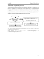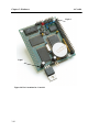
1
A-Core86™ 16-bit Controller with 16-bit SRAM & Flash, 16-bit ADC, DAC, and I/Os Based on the 40MHz Am186ES Technical Manual 1724 Picasso Avenue, Davis, CA 95616, USA Tel: 530-758-0180 Fax: 530-758-0181 Email: [email protected] http://www.tern.com COPYRIGHT A-Core86, A-Core, A-Engine, i386-Engine, MemCard-A, VE232, and ACTF are trademarks of TERN, Inc. Am188ES and Am186ES are trademarks of Advanced Micro Devices, Inc. Paradigm C/C++ is a trademark of Paradigm Systems. MS-DOS, Windows95/9/2000/NT/XP are trademarks of Microsoft Corporation. IBM is a trademark of International Business Machines Corporation. Version 2.0 August 8, 2002 No part of this document may be copied or reproduced in any form or by any means without the prior written consent of TERN, Inc. © 1999 1724 Picasso Avenue, Davis, CA 95616, USA Tel: 530-758-0180 Fax: 530-758-0181 Email: [email protected] http://www.tern.com Important Notice TERN is developing complex, high technology integration systems. These systems are integrated with software and hardware that are not 100% defect free. TERN products are not designed, intended, authorized, or warranted to be suitable for use in life-support applications, devices, or systems, or in other critical applications. TERN and the Buyer agree that TERN will not be liable for incidental or consequential damages arising from the use of TERN products. It is the Buyer's responsibility to protect life and property against incidental failure. TERN reserves the right to make changes and improvements to its products without providing notice. A-Core86 Chapter 1: Introduction Chapter 1: Introduction 1.1 Functional Description Measuring 2.3 x 2.2 x 0.3 inches, the A-Core86™ (AC86) is a C/C++ programmable microprocessor core module with a 16-bit 40 MHz CPU (Am186ES, AMD). The AC86 is ideal for industrial process control and high speed data acquisition. The AC86 supports a 16-bit external data bus with up to 256 KB 16-bit battery-backed SRAM and a 256 KB 16-bit Flash. All chips are surface-mount to ensure highest reliability. The on-board Flash can be easily programmed in the field via serial link. The user can download AE86_115.HEX file for remote debugging with TERN’s EV-P/DV-P Kit. For OEM, the application code can be easily programmed into the Flash with the DV-P and ACTF Flash Kit. The A-Core86™ is based on the AMD Am186ES CPU. It supports x86 architecture and can operate externally in an 8-bit or 16-bit mode to accommodate 8 or 16-bit peripherals. The Am186ES provides two asynchronous serial ports which support full-duplex 7, 8, or 9-bit communication at baud rates up to 115,200. The AM186ES also offers 8 external interrupts with programmable priority levels and maskability. The Am186ES also provides three 16-bit programmable timers/counters and a watchdog timer. Two timers can be used to count external events, up to 10 MHz, or to generate PWM outputs. Pulse Width Demodulation (PWD) can be used to measure the width of a signal in both its high and low phases. The Am186ES CPU offers 32 user-programmable multifunctional I/O pins. Depending on the application, 20+ I/O lines may be free for the user. A supervisor chip (691) monitors power failure, reset, and watchdog. An optional 16-bit, 100K samples per second ADC (LTC1605) can be installed on the AC86. The 16-bit ADC has a ±10V bipolar input range with an internal reference. This easy-to-use device includes sampleand-hold, precision reference, switched capacitor successive approximation A/D, and trimmed internal clock. The ADC has an industry standard ±10V input range. An optional 2 channel 12-bit DAC (LT1446) provides 0 to +4.095V analog voltage output. It uses a serial interface, requires 5 us settling time, offers millivolt output resolution, and is capable of sinking or sourcing 5 mA. The A-Core86 has an on-board 512 byte EEPROM. This non-volatile storage can by used for node addresses, calibration coefficients, etc. The EEPROM has a lifetime of up tp 1,000,000 read /writes. A Real Time Clock (Epson, RTC72423) can be installed on the A-Core86™. It provides information on the year, month, date, hour, minute, and second, and an interrupt signal. Figure 1.1 features a functional block diagram for the AC86. 1-1 A-Core86 Chapter 1: Introduction A-Core86 SRAM J7 TxD RxD Am186ES CPU RS232 SER0 & SER1 256Kx16 40MHz FLASH 256Kx16 EEPROM 512 BYTES non-volatile RTC DMA(2) 16-Bit Timers(3) Ext. Interrupts(8) 32 I/O lines PWM/PWD 16-bit Ext. data bus Asynch. UARTs (2) 16-bit ADC LTC1605 12-bit 2ch. serial DAC J2 Header UARTs, Interrupts, PIO MAX691 Supervisor (watchdog, reset, power fail) H1 J1 Header Address / Data Expansion Bus Figure 1.1 Functional block diagram of the A-Core86 1.2 Features Standard Features • Dimensions: 2.3 x 2.2 x 0.3 inches • Power consumption: 190 mA at 5V for 40 MHz • Power-save mode: 30 mA at 5V for 40 MHz • Power input: +5V regulated DC, or + 9V to +12V unregulated DC with on-board regulator or VE232 • Temperature: -40°C to +80°C • 40 MHz, 16-bit CPU (Am186ES), program in C/C++ • 256 KW ACTF Flash (256K x 16) • 64 KW SRAM (64K x 16) • 16-bit external data bus expansion port • Up to 340 MB memory expansion via MemCard-A or FlashCore-0™ • 2 asynchronous serial ports that support 7, 8, or9-bit communication • 2 PWM outputs, 1 PWD input, • 3 16-bit timers/counters • 8 external interrupts with programmable priority • 32 multifunctional I/O lines from Am186ES • 512-byte EEPROM 1-2 A-Core86 Chapter 1: Introduction Optional Features • 100 KHz 16-bit ADC, LTC1605 • 256 KW SRAM (256K x 16) • 2 channels 12-bit DAC (LT1446) • Real-time clock (RTC72423), lithium coin battery • 2 RS-232 drivers and 5V regulator 1.3 Physical Description H1 & H2 Headers Analog Input for ADC Analog Output for DAC 2 Channel, 12-bit Serial DAC 100KHz 16-bit ADC J7 Header SER0 (default debug port), SER1 J2 Header External Interrupt lines, RxD, TxD, PIOs EEPROM 512-btye J1 Header Address / Data Expansion Bus Step 2 Jumper Location (J2 pins 38 & 40) 16-bit SRAM Up to 256 KW 256 KW ACTF Flash MAX691 Supervisor +12V Unregulated Input (Only when 5V Regulator installed) +5V Regulator Input: Up to +12V . 1-3 A-Core86 Chapter 1: Introduction 1.4 A-Core86 Programming Overview The ACTF loader in the Flash will perform the system initialization and prepare for new application code download or immediately run the pre-loaded code. A remote debugger kernel can be loaded into the Flash at a starting address of 0xfa000. Two debug kernels are available to debug at different BAUDs. For a debugging baud rate of 115,200, the file “AE86_115.HEX” should be used. A baud rate of 38,400 requires the file “AE86_384.HEX”. A loader file, L_TDREM.HEX, and both debugger files, AE86_115.HEX and AE86_384.HEX, are included in the EV-P/DV-P disk under the c:\tern\186\rom\ae86 directory. A functional diagram of the ACTF (embedded in the AC86) is shown below: Power on or Reset STEP2 Jumper on ? J2 pin 38=P4=GND ? SEND out MENU over SER0 at 19200, N, 8, 1 to Hyper Terminal of Windows95/98/2000/NT/XP No Text command or download new codes Yes Read EE for the jump address CS:IP Process Commands See ACTF-kit and Functions for detail RUN the program starting at the CS:IP The C function prototypes supporting Am188/186ES hardware can be found in header file “ae.h”, in the c:\tern\186\include directory. Sample programs can be found c:\tern\186\samples\ac86 directories. in the c:\tern\186\samples\ae and 1-4 A-Core86 Chapter 1: Introduction Preparation for Debugging • Connect AC86 to PC via RS-232 link, 19,200, 8, N, 1 • Power on AC86 without STEP 2 jumper installed. Step 2 jumper is located at J2 pins 38, 40 • ACTF menu will be sent to PC terminal • Use “D” command to begin download. Select “Send Text File”. Go to c:\tern\186\rom\ae86 and send “l_tdrem.hex”. • Use “G” command to run “L_TDREM”. Type G04000 at terminal. Will erase Flash • Download “AE86_115.HEX”. Found in same directory. Will download beginning at 0xfa000 in flash • Reset AC86. Type “Gfa000” to set EE jump address to CS:IP = fa00:0000. • Install the STEP2 jumper (J2.38-40) • Reset AC86, Ready for Remote debugging STEP 1: Debugging • Launch Paradigm C/C++. Write your application. Refer to samples. Compile, link, download, and remote debug using Paradigm C/C++. STEP 2: Standalone Field Test • Run controller standalone, away from PC, with application downloaded into SRAM. Reset CS:IP to point to code in SRAM. • Power on without step 2 jumper. Menu will be sent to terminal. Type “G08000” to set CS:IP = 0800:0000. • Set step 2 jumper. Power-on / Reset. • CPU will execute code at CS:IP in SRAM, Test application. STEP 3: Production Development Kit Only • Generate application HEX file with DV-P based on field tested source code. • Power-on / Reset without step 2 jumper. Menu sent to terminal. • Use “D” command to download “L_29F400.hex”. Will prepare flash for application. • Send application HEX file. • Modify CS:IP to point to application in flash, 0x80000 • Power-on / Reset. You application will execute at startup out of flash. 1-5 A-Core86 Chapter 1: Introduction There is no ROM socket on the AC86. The User’s application program must reside in SRAM for debugging and reside in battery-backed SRAM for the standalone field test. The on-board Flash 29F400BT has 256K words of 16-bits each. It is divided into 11 sectors, comprised of one 16KB, two 8KB, one 32KB, and seven 64KB sectors. The top 16KB sector is pre-loaded with ACTF boot strip, the one 8KB sector starting 0xfa000 is for loading remote debugger kernel, and all remaining sectors are free for application use. The top 16KB ACTF boot strip is protected. Two utility HEX files, “L_TDREM.HEX” and “L_29F400.HEX”, are designed for downloading into SRAM starting at 0x04000 with ACTF-PC-HyperTerminal. Use the “D” command to download, and use the “G” command to run. “L_TDREM.HEX” will erase the 8KB sector and load a “AE86_115.HEX” or “AE86_384.HEX”. “L_29F400.HEX” will erase the remaining sectors for downloading your application HEX file. The following figure shows the memory mapping of the on-board SRAM and Flash. Figure is not drawn to scale. Top Sector (16KB) ACTF Utility Protected ACTF Utility 8KB sector for debug kernel. Can be erased by “l_tdrem.hex” Debug Kernel ae86_115 0xFFFFF 0xFC000 Flash 0xFA000 Remaining sectors for application. Can be erased by “l_29f400.hex” 0x80000 SRAM 0x20000 0x00000 For production, the user must produce an ACTF-downloadable HEX file for the application, based on the DV-P+ACTF Kit. The application HEX file can be loaded into the on-board Flash starting address at 0x80000. The on-board EE must be modified with a “G80000” command while in the ACTF-PC-HyperTerminal Environment. 1-6 A-Core86 Chapter 1: Introduction The “STEP2” jumper (J2 pins 38-40) must be installed for every production-version board. In order to correctly download a program in STEP1 with Paradigm C/C++, the AC86 must meet these requirements: 1) AE86_115.HEX must be pre-loaded into Flash starting address 0xfa000. 2) The SRAM installed must be large enough to hold your program. For a 128K SRAM, the physical address is 0x00000-0x01ffff For a 512K SRAM, the physical address is 0x00000-0x07ffff 3) The on-board EE must have a correct jump address for the AE86_115.HEX with starting address of 0xfa000. 4) The STEP2 jumper must be installed on J2 pins 38-40. 1.5 Minimum Requirements for AC86 System Development 1.5.1 Minimum Hardware Requirements • • • • PC or PC-compatible computer with serial COMx port that supports 115,200 baud A-Core86 controller PC-V25 serial cable (RS-232; DB9 connector for PC COM port and IDE 2x5 connector for controller) Center negative wall transformer (+9V, 500 mA) 1.5.2 Minimum Software Requirements • TERN EV-P/DV-P installation CD-ROM and a PC running: Windows 95/98/2000/NT/XP With the EV-P, you can program and debug the A-Core86 in Step One and Step Two, but you cannot run Step Three. In order to generate an application Flash file and complete a project, you will need both the Development Kit (DV-P Kit) and the ACTF Flash Kit. 1-7 A-Core86 Chapter 2: Installation Chapter 2: Installation 2.1 Software Installation Please refer to the Technical Manual for the “C/C++ Development Kit for TERN 16-bit Embedded Microcontrollers” for information on installing software. The README.TXT file on the TERN EV-P/DV-P disk contains important information about the installation and evaluation of TERN controllers. 2.2 Hardware Installation Overview • Connect PC-V25 cable: For debugging (Step One), place ICD connector on J7 (SER0) with red edge of cable at pin 1 • Connect wall transformer: Connect 9V wall transformer to power and plug into power jack adapter. Plug power jack adapter onto J3 on AC86 (2-pin header) . Hardware installation for the A-Core86 consists primarily of connecting the microcontroller to your PC and to power. The debug serial cable must be installed to an open COMx port on the PC side and then to the debug serial port of you AC86, SER0, which is located at J7. Confirm that the red edge fo the cable points to pin 1 of the J7 header. 2.2.1 Connecting the A-Core86 to the PC The following diagram (Figure 2.1) illustrates the connection between the A-Core86 and the PC. The ACore86 is linked to the PC via a serial cable (PC-V25). 2-1 Chapter 2: Installation To COMx on PC side at 19200 Baud A-Core86 Debug Port SER 0 Red Edge of cable points to J7 pin1 Figure 2.1 Serial connection between the A-Core86 and the PC for debugging (Step One) 2.2.2 Powering-on the A-Core86 Before connecting any power source to the A-Core86, make sure to verify that the polarity of the input power source matches the polarity of the power input jack of the A-Core86. Connect a wall transformer +9V DC output to the AC86 DC power jack adapter. The on-board LED should blink twice and remain on after the A-Core86 is powered on or reset (Error! Reference source not found.). 2-2 A-Core86 Chapter 2: Installation Be sure to verify polarity before applying power ! Figure 2.2 Location of J0 power jack for +9V DC input CAUTION: The CPU and the power regulator on the A-Core86 can become very hot while the power is connected. 2-3 A-Core86 Chapter 3: Hardware Chapter 3: Hardware 3.1 Am186ES – Introduction The Am186ES is based on industry-standard x86 architecture. The Am186ES controllers are higherperformance, more integrated versions of the 80C188 microprocessors. In addition, the Am186ES has new peripherals. The on-chip system interface logic can minimize total system cost. The Am186ES has two asynchronous serial ports, 32 PIOs, a watchdog timer, additional interrupt pins, a pulse width demodulation option, DMA to and from serial ports, a 16-bit reset configuration register, and enhanced chip-select functionality. 3.2 Am186ES – Features 3.2.1 Clock Due to its integrated clock generation circuitry, the Am186ES microcontroller allows the use of a timesone crystal frequency. The design achieves 40 MHz CPU operation, while using a 40 MHz crystal. The system CLKOUTA and CLKOUTB signals are not routed to external pins. 3.2.2 External Interrupts There are eight external interrupts: INT0-INT6 and NMI. INT0, J2 pin 8 INT1, J2 pin 6 INT2, J2 pin 19 INT3, J2 pin 21 INT4, J2 pin 33 INT5=P12=DRQ0, J2 pin 5, used by A-Core86 as output for LED/EE/HWD/DAC/ADC INT6 = P13, J2 pin 11 NMI, J2 pin 7 By hardware reset default, all interrupts are edge triggered and require a LOW-TO-HIGH transition. INT5 is a multiplexed pin, shared with DRQ0 and P12. It is strongly recommended by TERN that the user not use this line in any part in their application, since it is already used by the system for the LED, EEPROM, DAC, ADC, and Watchdog timer. Attempting to initialize this line in any way could severely affect the reliabililty of other on-board peripherals. The user can modify the interrupt control registers to make interrupts level-sensitive (INT5 and INT6 are edge-triggered only). Refer to Chapter 7 of the Am186ES technical manual in the tern_docs\amd_docs directory on your CD. Six external interrupt inputs, INT0-4 and NMI, are tied to pull-down resistors using a resistor network (RN1). The A-Core86 uses vector interrupt functions to respond to external interrupts. Refer to the Am186ES User’s manual for information about interrupt vectors. 3-1 Chapter 3: Hardware A-Core86 3.2.3 Asynchronous Serial Ports The Am186ES CPU has two asynchronous serial channels: SER0 and SER1. Both asynchronous serial ports support the following: • • • • • • • • • • • Full-duplex operation 7-bit, 8-bit, and 9-bit data transfers Odd, even, and no parity One stop bit Error detection Hardware flow control DMA transfers to and from serial ports Transmit and receive interrupts for each port Multidrop 9-bit protocol support Maximum baud rate of 1/16 of the CPU clock speed Independent baud rate generators The software drivers for each serial port implement a ring-buffered DMA receiving and ring-buffered interrupt transmitting arrangement. See the samples files s1_echo.c and s0_echo.c. 3.2.4 Timer Control Unit The timer/counter unit has three 16-bit programmable timers: Timer0, Timer1, and Timer2. Timer0 and Timer1 are connected to four external pins: Timer0 output = P10 = J2 pin 12 Timer0 input = P11 = J2 pin 14 Timer1 output = P1 = J2 pin 29 = J1 pin 4 Timer1 input = P0 = J2 pin 20 These two timers can be used to count or time external events, or they can generate non-repetitive or variable-duty-cycle waveforms. Timer2 is not connected to any external pin. It can be used as an internal timer for real-time coding or time-delay applications. It can also prescale timer 0 and timer 1 or be used as a DMA request source. The maximum rate at which each timer can operate is 10 MHz, since each timer is serviced once every fourth clock cycle. Timer output takes up to six clock cycles to respond to clock or gate events. See the sample programs timer0.c and ae_cnt0.c in the 186\samples\ae directory. 3.2.5 PWM outputs and PWD The Timer0 and Timer1 outputs can also be used to generate non-repetitive or variable-duty-cycle waveforms. The timer output takes up to 6 clock cycles to respond to the clock input. Thus the minimum timer output cycle is 25 ns/clock x 6 clocks = 150 ns (at 40 MHz CPU clock). Each timer has a maximum count register that defines the maximum value the timer will reach. Both Timer0 and Timer1 have secondary maximum count registers for variable duty cycle output. Using both the primary and secondary maximum count registers lets the timer alternate between two maximum values. 3-2 A-Core86 Chapter 3: Hardware MAX. COUNT A MAX. COUNT B Pulse Width Demodulation can be used to measure the input signal’s high and low phases on the INT2=J2 pin 19. Refer to Section 8.2 of the Am186ES technical manual for more information on Pulse Width Demodulation. 3.2.6 Power-save Mode The A-Core86 is an ideal core module for low power consumption applications. The power-save mode of the Am186ES reduces power consumption and heat dissipation, thereby extending battery life in portable systems. In power-save mode, operation of the CPU and internal peripherals continues at a slower clock frequency. When an interrupt occurs, it automatically returns to its normal operating frequency. The RTC72423 on the A-Core86 has a VOFF signal routed to J1 pin 9. VOFF is controlled by the batterybacked RTC72423. The VOFF signal can be programmed by software to be in tri-state or to be active low. The RTC72423 can be programmed in interrupt mode to drive the VOFF pin at 1 second, 1 minute, or 1 hour intervals. The user can use the VOFF line to control an external switching power supply that turns the power supply on/off. More details are available in the sample file poweroff.c in the 186\samples\ae sub-directory. 3.3 Am186ES PIO lines The Am186ES has 32 pins available as user-programmable I/O lines. Each of these pins can be used as a user-programmable input or output signal, if the normal shared function is not needed. A PIO line can be configured to operate as an input or output with or without a weak pull-up or pull-down, or as an opendrain output. A pin’s behavior, either pull-up or pull-down, is pre-determined and shown in the table below. After power-on/reset, PIO pins default to various configurations. The initialization routine provided by TERN libraries reconfigures some of these pins as needed for specific on-board usage, as well. These configurations, as well as the processor-internal peripheral usage configurations, are listed below in Table 3.1. PIO Function Power-On/Reset status A-Core86 Pin No. A-Core86 Initial P0 P1 P2 P3 P4 P5 P6 P7 P8 P9 Timer1 in Timer1 out /PCS6/A2 /PCS5/A1 DT/R /DEN/DS SRDY A17 A18 A19 Input with pull-up Input with pull-down Input with pull-up Input with pull-up Normal Normal Normal Normal Normal Normal J2 pin 20 J2 pin 29 J2 pin 24 J2 pin 15 J2 pin 38 J2 pin 30 J2 pin 35 N/A N/A N/A Input with pull-up Output RTC select Output Input with pull-up Step 2 Input with pull-up Input with pull-down A17 A18 A19 3-3 Chapter 3: Hardware A-Core86 PIO Function Power-On/Reset status A-Core86 Pin No. A-Core86 Initial P10 P11 P12 P13 P14 P15 P16 P17 P18 P19 P20 P21 P22 P23 P24 P25 P26 P27 P28 P29 P30 P31 Timer0 out Timer0 in DRQ0/INT5 DRQ1/INT6 /MCS0 /MCS1 /PCS0 /PCS1 CTS1/PCS2 RTS1/PCS3 RTS0 CTS0 TxD0 RxD0 /MCS2 /MCS3 UZI TxD1 RxD1 /CLKDIV2 INT4 INT2 Input with pull-down Input with pull-up Input with pull-up Input with pull-up Input with pull-up Input with pull-up Input with pull-up Input with pull-up Input with pull-up Input with pull-up Input with pull-up Input with pull-up Input with pull-up Input with pull-up Input with pull-up Input with pull-up Input with pull-up Input with pull-up Input with pull-up Input with pull-up Input with pull-up Input with pull-up J2 pin 12 J2 pin 14 J2 pin 5 J2 pin 11 J2 pin 37 J2 pin 23 J1 pin 19 J2 pin 13 J2 pin 22 J2 pin 31 J2 pin 27 J2 pin 36 J2 pin 34 J2 pin 32 J2 pin 17 J2 pin 18 J2 pin 4 J2 pin 28 J2 pin 26 J2 pin 3 J2 pin 33 J2 pin 19 Input with pull-down Input with pull-up Output for LED/EE/HWD Input with pull-up Input with pull-up Input with pull-up /PCS0 DAC select Input with pull-up Input with pull-up Input with pull-up Input with pull-up TxD0 RxD0 Input with pull-up Input with pull-up Input with pull-up* TxD1 RxD1 Input with pull-up* Input with pull-up Input with pull-up * Note: P26 and P29 must NOT be forced low during power-on or reset. Table 3.1 I/O pin default configuration after power-on or reset Three external interrupt lines are not shared with PIO pins: INT0 = J2 pin 8 INT1 = J2 pin 6 INT3 = J2 pin 21 The 32 PIO lines, P0-P31, are configurable via two 16-bit registers, PIOMODE and PIODIRECTION. The settings are as follows: MODE 0 1 2 3 PIOMODE reg. 0 0 1 1 PIODIRECTION reg. 0 1 0 1 PIN FUNCTION Normal operation INPUT with pull-up/pull-down OUTPUT INPUT without pull-up/pull-down A-Core86 initialization on PIO pins in ae_init() is listed below: outport(0xff78,0xe73c); // PDIR1, TxD0, RxD0, TxD1, RxD1, P16=PCS0, P17=PCS1=PPI outport(0xff76,0x0000); // PIOM1 outport(0xff72,0xec7b); // PDIR0, P12,A19,A18,A17,P2=PCS6=RTC outport(0xff70,0x1000); // PIOM0, P12=LED The C function in the library ae_lib can be used to initialize PIO pins. void pio_init(char bit, char mode); 3-4 A-Core86 Chapter 3: Hardware Where bit = 0-31 and mode = 0-3, see the table above. Example: pio_init(12, 2); will set P12 as output pio_init(1, 0); will set P1 as Timer1 output void pio_wr(char bit, char dat); pio_wr(12,1); set P12 pin high, if P12 is in output mode pio_wr(12,0); set P12 pin low, if P12 is in output mode unsigned int pio_rd(char port); pio_rd (0); return 16-bit status of P0-P15, if corresponding pin is in input mode, pio_rd (1); return 16-bit status of P16-P31, if corresponding pin is in input mode, Some of the I/O lines are used by the A-Core86 system for on-board components (Table 3.2). We suggest that you not use these lines unless you are sure that you are not interfering with the operation of such components (i.e., if the component is not installed). Signal P1 P2 P4 P11 P12 P17 P22 P23 P26 P29 Pin Timer1 output /PCS6 /DT Timer0 input DRQ0/INT5 /PCS1 TxD0 RxD0 Function U4 RTC72423 chip select at base I/O address 0x0600 Step Two jumper U7 24C04 EE data input Output for LED, U7 serial EE clock, Hit watchdog, ADC, DAC Chip select for U12 ADC; I/O map to 0x0100 Default SER0 debug Default SER0 debug Data In for DAC 1446 Latch Data for DAC 1446 Table 3.2 I/O lines used for on-board components 3.4 I/O Mapped Devices 3.4.1 I/O Space External I/O devices can use I/O mapping for access. You can access such I/O devices with inportb(port) or outportb(port,dat). These functions will transfer one byte or word of data to the specified I/O address. The external I/O space is 64K, ranging from 0x0000 to 0xffff. The default I/O access time is 15 wait states. You may use the function void io_wait(char wait) to define the I/O wait states from 0 to 15. The system clock is 25 ns, giving a clock speed of 40 MHz. Details regarding this can be found in the Software chapter, and in the Am186ES User’s Manual. Slower components, such as most LCD interfaces, might find the maximum programmable wait state of 15 cycles still insufficient. Due to the high bus speed of the system, some components need to be attached to I/O pins directly. For details regarding the chip select unit, please see Chapter 5 of the Am186ES User’s Manual. The table below shows more information about I/O mapping. 3-5 Chapter 3: Hardware A-Core86 I/O space Select Location Usage 0x0000-0x00ff 0x0100-0x01ff 0x0200-0x02ff 0x0300-0x03ff 0x0400-0x04ff 0x0500-0x05ff 0x0600-0x06ff /PCS0 /PCS1 /PCS2 /PCS3 /PCS4 /PCS5 /PCS6 J1 pin 19=P16 J2 pin 13=P17 J2 pin 22=CTS1 J2 pin 31=RTS1 USER* DAC USER USER Reserved USER RTC 72423 J2 pin 15=P3 J2 pin 24=P2 *PCS0 may be used for other TERN peripheral boards. To illustrate how to interface the A-Core86 with external I/O boards, a simple decoding circuit for interfacing to an 82C55 parallel I/O chip is shown in Figure 3.1. 82C55 74HC138 RST P00-P07 A5 1 Y0 15 NC A A0 A6 2 Y1 14 /SEL20 A1 B 3 Y2 13 /SEL40 A7 C Y3 12 /SEL60 /SEL20 /CS P10-P17 Y4 11 /SEL80 /WR /WR G2A 4 Y5 10 /SELA0 /PCS0 5 G2B Y6 9 /SELC0 /RD /RD VCC 6 G1 Y7 7 /SELF0 P20-P27 D0-D7 Figure 3.1 Interface the A-Core86 to external I/O devices The function ae_init() by default initializes the /PCS0 line at base I/O address starting at 0x00. You can read from the 82C55 with inportb(0x020) or write to the 82C55 with outportb(0x020,dat). The call to inportb(0x020) will activate /PCS0, as well as putting the address 0x00 over the address bus. The decoder will select the 82C55 based on address lines A5-7, and the data bus will be used to read the appropriate data from the off-board component. 3.4.2 Real-time Clock RTC72423 If installed, the real-time clock RTC72423 (EPSON, U10) is mapped in the I/O address space 0x0600. It must be backed up with a lithium coin battery. The RTC is accessed via software drivers rtc_init() or rtc_rd(). It is also possible to configure the real-time clock to raise an output line attached to an external interrupt, at 1/64 second, 1 second, 1 minute, or 1 hour intervals. This can be used in a time-driven application, or the VOFF signal can be used to turn on/off the controller using an external switching power supply. An example of a program showing a similar application can be found in tern\186\samples\ae\poweroff.c. 3.5 Other Devices A number of other devices are also available on the A-Core86. Some of these are optional, and might not be installed on the particular controller you are using. For a discussion regarding the software interface for these components, please see the Software chapter. 3-6 A-Core86 Chapter 3: Hardware 3.5.1 On-board Supervisor with Watchdog Timer The MAX691/LTC691 (U6) is a supervisor chip. With it installed, the A-Core86 has several functions: watchdog timer, battery backup, power-on-reset delay, and power-supply monitoring. These will significantly improve system reliability. Watchdog Timer The watchdog timer is activated by setting a jumper on J9 of the A-Core86. The watchdog timer provides a means of verifying proper software execution. In the user's application program, calls to the function hitwd() (a routine that toggles the P12=HWD pin of the MAX691) should be arranged such that the HWD pin is accessed at least once every 1.6 seconds. If the J9 jumper is on and the HWD pin is not accessed within this time-out period, the watchdog timer pulls the WDO pin low, which asserts /RESET. This automatic assertion of /RESET may recover the application program if something is wrong. After the ACore86 is reset, the WDO remains low until a transition occurs at the WDI pin of the MAX691. When controllers are shipped from the factory the J9 jumper is off, which disables the watchdog timer. The Am186ES has an internal watchdog timer. This is disabled by default with ae_init(). Location of J9. Wathcdog Timer Enable Figure 3.2 Location of watchdog timer enable jumper Power-failure Warning The supervisor supports power-failure warning and backup battery protection. When power failure is sensed by the PFI, pin 9 of the MAX691 (lower than 1.3 V), the PFO is low. The PFI pin 9 of 691 is directly short to VCC by default. In order to use PFI externally, cut the trace and bring the PFI signal out. You may design an NMI service routine to take protect actions before the +5V drops and processor dies. The following circuit shows how you might use the power-failure detection logic within your application. 3-7 Chapter 3: Hardware A-Core86 9-14 V (8.35 V min) 47K 2K VCC = +5V C? PFI, pin 9 of MAX691 (1.3 V min) Figure 3.3 Using the supervisor chip for power failure detection Battery Backup Protection The backup battery protection protects data stored in the SRAM and RTC. The battery-switch-over circuit compares VCC to VBAT (+3 V lithium battery positive pin), and connects whichever is higher to the VRAM (power for SRAM and RTC). Thus, the SRAM and the real-time clock RTC72423 are backed up. In normal use, the lithium battery should last about 3-5 years without external power being supplied. When the external power is on, the battery-switch-over circuit will select the VCC to connect to the VRAM. 3.5.2 EEPROM A serial EEPROM of 512 bytes (24C04) is installed in U7. The A-Core86 uses the P12=SCL (serial clock) and P11=SDA (serial data) to interface with the EEPROM. The EEPROM can be used to store important data such as a node address, calibration coefficients, and configuration codes. It typically has 1,000,000 erase/write cycles. The data retention is more than 40 years. EEPROM can be read and written by simply calling the functions ee_rd() and ee_wr(). A range of lower addresses in the EEPROM is reserved for TERN use. The address range 0x000 – 0x01F is reserved for use by TERN. The address range 0x020 – 0x1FF is for application use. 3.5.3 Dual 12-bit DAC (LTC1446) The LTC1446 is a dual 12-bit digital-to-analog converter (DAC) in an SO-8 package. It is complete with a rail-to-rail voltage output amplifier, an internal reference and a 3-wire serial interface. The LTC1446 outputs a full-scale of 4.096V, making 1 LSB equal to 1 mV. The buffered outputs can source or sink 5 mA. The outputs swing to within a few millivolts of supply rail when unloaded. They have an equivalent output resistance of 40 Ω when driving a load to the rails. The buffer amplifiers can drive 1000 pf without going into oscillation. The DAC is installed in U12 on the AC86, and the outputs are routed to H2 pin 1 for DAC channel A, and H2 pin 2 for DAC channel B. The DAC uses P12 a clock, P26 for Data In, and P29 for Latch Data. Please refer to the LT1446 technical data sheets found on the TERN CD under the tern_docs\parts directory. See also the sample program ae_da.c in the tern\186\samples\ae directory. 3.5.4 LTC1605, 100K Hz, 16-bit ADC The LTC1605 is a 100 ksps, sampling 16-bit A/D converter that draws only 55 mW from a single 5V supply. This device includes sample-and-hold, precision reference, switched capacitor successiveapproximation A/D, and trimmed internal clock. 3-8 A-Core86 Chapter 3: Hardware The input range of the LTC1605 is an industry standard ±10V. Maximum DC specs include ±2.0 LSB INL and 16-bit no missing codes over temperature. An external reference can be used if greater accuracy is needed. The ADC has a microprocessor compatible, 16-bit or 2-byte parallel output port. The AC86 uses P12 to control the ADC’s R/C pin and directly interface the full 16-bit data bus for maximum data transfer rate. The LTC1605 requires 8 µs AD conversion time. The busy signal has an 8 µs low period indicating the conversion in process. In order to achieve the 100 KHz sample rate, AC86 cannot use interrupt operation to acquire data. A polling method, using timer2 as the 10 µs timebase, is demonstrated in the sample program ac_ad16.c, found in the c:\tern\186\samples\ac86 directory 3.6 Headers and Connectors 3.6.1 Expansion Headers J1 and J2 There are two 20x2 0.1 spacing headers for A-Core86 expansion. Most signals are directly routed to the Am186ES processor. These signals are 5V only, and any out-of-range voltages will most likely damage the board. 3-9 Chapter 3: Hardware A-Core86 J2 pin 1 J1 pin 1 Figure 3.4 Pin 1 locations for J1 and J2 3-10 A-Core86 Chapter 3: Hardware J1: 1 3 5 7 9 11 13 15 17 19 21 23 25 27 29 31 33 35 37 39 VCC VOFF /BHE D15 /RST RST P16 D14 D13 D12 /WR /RD D11 D10 D9 D8 GND GND D0 D1 D2 D3 D4 D5 D6 D7 GND A7 A6 A5 A4 A3 A2 A1 A0 2 4 6 8 10 12 14 16 18 20 22 24 26 28 30 32 34 36 38 40 J2: 40 38 36 34 32 30 28 26 24 22 20 18 16 14 12 10 8 6 4 2 GND P4 /CTS0 TXD0 RXD0 P5 TXD1 RXD1 P2 /CTS1 P0 P25 P11 P10 VCC P14 P6 INT4 /RTS1 P1 /RTS0 ALE P15 INT3 INT2 P24 P3 P17 P13 INT0 INT1 P26 GND NMI P12 P29 GND 39 37 35 33 31 29 27 25 23 21 19 17 15 13 11 9 7 5 3 1 Table 3.3 Signals for J1 and J2, 20x2 expansion ports 3-11 Chapter 3: Hardware A-Core86 Signal definitions for J1: VCC GND VOFF D0-D15 A0-A7 /BHE /RST RST P16 /WR /RD +5V power supply Ground Output of RTC72423 U4, open collector Am186ES 16-bit external data lines Am186ES address lines Byte High Enable, Active low reset signal, active low reset signal, active high /PCS0, Am186ES pin 66 Am186ES pin 5 Am186ES pin 6 Signal definitions for J2: VCC GND Pxx ALE TxD0 RxD0 TxD1 RxD1 /CTS0 /CTS1 /RTS0 /RTS1 INT0-4 NMI 3-12 +5V power supply, < 200 mA ground Am186ES PIO pins Am186ES pin 7, address latch enable Am186ES pin 2, transmit data of serial channel 0 Am186ES pin 1, receive data of serial channel 0 Am186ES pin 98, transmit data of serial channel 1 Am186ES pin 99, receive data of serial channel 1 Am186ES pin 100, Clear-to-Send signal for SER0 Am186ES pin 63, Clear-to-Send signal for SER1 Am186ES pin 3, Request-to-Send signal for SER0 Am186ES pin 62, Request-to-Send signal for SER1 Schmitt-trigger inputs Non-maskable interrupt A-Core86 Chapter 4: Software Chapter 4: Software Please refer to the Technical Manual of the “C/C++ Development Kit for TERN 16-bit Embedded Microcontrollers” for details on debugging and programming tools. For details regarding software function prototypes and sample files demonstrating their use, please refer to the Software Glossary in Appendix F of the A-Engine technical manual, found in the tern_docs\manuals directory. Guidelines, awareness, and problems in an interrupt driven environment Although the C/C++ Development Kit provides a simple, low cost solution to application engineers, some guidelines must be followed. If they are not followed, you may experience system crashes, PC hang-ups, and other problems. The debugging of interrupt handlers with the Remote Debugger can be a challenge. It is possible to debug an interrupt handler, but there is a risk of experiencing problems. Most problems occur in multi-interruptdriven situations. Because the remote kernel running on the controller is interrupt-driven, it demands interrupt services from the CPU. If an application program enables interrupt and occupies the interrupt controller for longer than the remote debugger can accept, the debugger will time-out. As a result, your PC may hang-up. In extreme cases, a power reset may be required to restart your PC. For your reference, be aware that our system is remote kernel interrupt-driven for debugging. The run-time environment on TERN controllers consists of an I/O address space and a memory address space. I/O address space ranges from 0x0000 to 0xffff, or 64 KB. Memory address space ranges from 0x00000 to 0xfffff in real-mode, or 1 MB. These are accessed differently, and not all addresses can be translated and handled correctly by hardware. I/O and memory mappings are done in software to define how translations are implemented by the hardware. Implicit accesses to I/O and memory address space occur throughout your program from TERN libraries as well as simple memory accesses to either code or global and stack data. You can, however, explicitly access any address in I/O or memory space, and you will probably need to do so in order to access processor registers and on-board peripheral components (which often reside in I/O space) or non-mapped memory. This is done with four different sets of similar functions, described below. poke/pokeb Arguments: unsigned int segment, unsigned int offset, unsigned int/unsigned char data Return value: none These standard C functions are used to place specified data at any memory space location. The segment argument is left shifted by four and added to the offset argument to indicate the 20-bit address within memory space. poke is used for writing 16 bits at a time, and pokeb is used for writing 8 bits. The process of placing data into memory space means that the appropriate address and data are placed on the address and data-bus, and any memory-space mappings in place for this particular range of memory will be used to activate appropriate chip-select lines and the corresponding hardware component responsible for handling this data. 4-1 Chapter 4: Software A-Core86 peek/peekb Arguments: unsigned int segment, unsigned int offset Return value: unsigned int/unsigned char data These functions retrieve the data for a specified address in memory space. Once again, the segment address is shifted left by four bits and added to the offset to find the 20-bit address. This address is then output over the address bus, and the hardware component mapped to that address should return either an 8-bit or 16-bit value over the data bus. If there is no component mapped to that address, this function will return random garbage values every time you try to peek into that address. outport/outportb Arguments: unsigned int address, unsigned int/unsigned char data Return value: none This function is used to place the data into the appropriate address in I/O space. It is used most often when working with processor registers that are mapped into I/O space and must be accessed using either one of these functions. This is also the function used in most cases when dealing with user-configured peripheral components. When dealing with processor registers, be sure to use the correct function. Use outport if you are dealing with a 16-bit register. inport/inportb Arguments: unsigned int address Return value: unsigned int/unsigned char data This function can be used to retrieve data from components in I/O space. You will find that most hardware options added to TERN controllers are mapped into I/O space, since memory space is valuable and is reserved for uses related to the code and data. Using I/O mappings, the address is output over the address bus, and the returned 16 or 8-bit value is the return value. For a further discussion of I/O and memory mappings, please refer to the Hardware chapter of this technical manual. 4.1 Programming Overview The ACTF loader in the AC86 256KW Flash will perform the system initialization and prepare for new application code download or immediately run the pre-loaded code. A remote debugger kernel can be loaded into the Flash located starting 0xfa000. Debugging at baud rate of 115,200 (AE86_115.HEX) and 38,400 (AE86_384.HEX) are available. A loader file L_TDREM.HEX and both debugger files AE86_115.HEX and AE86_384.HEX, are included in the EV-P/DV-P disk under the c:\tern\186\rom\ae86 directory. 4-2 A-Core86 Chapter 4: Software A functional diagram of the ACTF (embedded in the AC86) is shown below: Power on or Reset STEP2 Jumper on ? J2 pin 38=P4=GND ? SEND out MENU over SER0 at 19200, N, 8, 1 to Hyperterminal of Windows95/98 No Text command or download new codes Yes Read EE for the jump address CS:IP Process Commands See ACTF-kit and Functions for detail RUN the program starting at the CS:IP The C function prototypes supporting Am186ES hardware can be found in header file “ae.h”, in the c:\tern\186\include directory. Sample programs can be found c:\tern\186\samples\ac86 directories. in the c:\tern\186\samples\ae and 4-3 Chapter 4: Software A-Core86 4.1.1 Steps for AC86-based product development Preparation for Debugging • Connect AC86 to PC via RS-232 link, 19,200, 8, N, 1 • Power on AC86 without STEP 2 jumper installed. Step 2 jumper is located at J2 pins 38, 40 • ACTF menu will be sent to PC terminal • Use “D” command to begin download. Select “Send Text File”. Go to c:\tern\186\rom\ae86 and send “l_tdrem.hex”. • Use “G” command to run “L_TDREM”. Type G04000 at terminal. Will erase Flash • Download “AE86_115.HEX”. Found in same directory. Will download beginning at 0xfa000 in flash • Reset AC86. Type “Gfa000” to set EE jump address to CS:IP = fa00:0000. • Install the STEP2 jumper (J2.38-40) • Reset AC86, Ready for Remote debugging STEP 1: Debugging • Launch Paradigm C/C++. Write your application. Refer to samples. Compile, link, download, and remote debug using Paradigm C/C++. STEP 2: Standalone Field Test • Run controller standalone, away from PC, with application downloaded into SRAM. Reset CS:IP to point to code in SRAM. • Power on without step 2 jumper. Menu will be sent to terminal. Type “G08000” to set CS:IP = 0800:0000. • Set step 2 jumper. Power-on / Reset. • CPU will execute code at CS:IP in SRAM, Test application. STEP 3: Production Development Kit Only • Generate application HEX file with DV-P based on field tested source code. • Power-on / Reset without step 2 jumper. Menu sent to terminal. • Use “D” command to download “L_29F400.hex”. Will prepare flash for application. • Send application HEX file. • Modify CS:IP to point to application in flash, 0x80000 • Power-on / Reset. You application will execute at startup out of flash. 4-4 A-Core86 Chapter 4: Software There is no ROM socket on the AC86. The user’s application program must reside in SRAM for debugging in STEP1, reside in battery-backed SRAM for the standalone field test in STEP2, and finally be programmed into Flash for a complete product (STEP 3). The on-board Flash 29F400BT has 256K words of 16-bits each. It is divided into 11 sectors, comprised of one 16KB, two 8KB, one 32KB, and seven 64KB sectors. The top one 16KB sector is pre-loaded with ACTF boot strip, the one 8KB sector starting 0xfa000 is for loading remote debugger kernel, and the reset all sectors are free for application use. The top 16KB ACTF boot strip is protected. Two utility HEX files, “L_TDREM.HEX” and “L_29F400.HEX”, are designed for downloading into SRAM starting at 0x04000 with ACTF-PC-HyperTerminal. Use the “D” command to download, and use the “G” command to run. “L_TDREM.HEX” will erase the 8KB sector and load “AE86_115.HEX” or “AE86_384.HEX”. “L_29F400.HEX” will erase the remaining sectors for downloading your application HEX file. Top Sector (16KB) ACTF Utility Protected ACTF Utility 8KB sector for debug kernel. Can be erased by “l_tdrem.hex” Debug Kernel ae86_115 0xFFFFF 0xFC000 Flash 0xFA000 Remaining sectors for application. Can be erased by “l_29f400.hex” 0x80000 SRAM 0x20000 0x00000 For production, the user must produce an ACTF-downloadable HEX file for the application, based on the DV-P+ACTF Kit. The application HEX file can be loaded into the on-board Flash starting address at 0x80000. The on-board EE must be modified with a “G80000” command while in the ACTF-PC-HyperTerminal Environment. The “STEP2” jumper (J2 pins 38-40) must be installed for every production-version board. 4-5 Chapter 4: Software A-Core86 Step 1 settings In order to correctly download a program in STEP1 with the ParadigmC/C++ Debugger, the AC86 must meet these requirements: 1) AE86_115.HEX must be pre-loaded into Flash starting address 0xfa000. 2) The SRAM installed must be large enough to hold your program. For a 128K SRAM, the physical address is 0x00000-0x01ffff For a 512K SRAM, the physical address is 0x00000-0x07ffff 3) The on-board EE must have a correct jump address for the AE86_115.HEX with starting address of 0xfa000. 4) The STEP2 jumper must be installed on J2 pins 38-40. 4.2 AE.LIB AE.LIB is a C library for basic A-Core86 operations. It includes the following modules: AE.OBJ, SER0.OBJ, SER1.OBJ, SCC.OBJ, and AEEE.OBJ. You need to link AE.LIB in your applications and include the corresponding header files. The following is a list of the header files: Include-file name Description AE.H SER0.H SER1.H SCC.H AEEE.H PPI, timer/counter, ADC, DAC, RTC, Watchdog Internal serial port 0 Internal serial port 1 External UART SCC2691 on-board EEPROM The UART SCC2691 is not available on the A-Core86, so “SCC.H” does not pertain to the A-Core86. 4.3 Functions in AE.OBJ 4.3.1 A-Core86 Initialization ae_init This function should be called at the beginning of every program running on A-Core86 core controllers. It provides default initialization and configuration of the various I/O pins, interrupt vectors, sets up expanded DOS I/O, and provides other processor-specific updates needed at the beginning of every program. There are certain default pin modes and interrupt settings you might wish to change. With that in mind, the basic effects of ae_init are described below. For details regarding register use, you will want to refer to the AMD Am186ES Microcontroller User’s manual. • 4-6 Initialize the upper chip select to support the default ROM. The CPU registers are configured such that: − Address space for the ROM is from 0x80000-0xfffff (to map MemCard I/O window) − 512K ROM Block size operation. − Three wait state operation (allowing it to support up to 120 ns ROMs). With 70 ns ROMs, this can actually be set to zero wait state if you require increased performance (at a risk of A-Core86 Chapter 4: Software stability in noisy environments). For details, see the UMCS (Upper Memory Chip Select Register) reference in the processor User’s manual. outport(0xffa0, 0x80bf); // UMCS, 512K ROM, 0x80000-0xfffff • Initialize LCS (Lower Chip Select) for use with the SRAM. It is configured so that: − Address space starts 0x00000, with a maximum of 512K RAM. − Three wait state operation. Reducing this value can improve performance. − Disables PSRAM, and disables need for external ready. outport(0xffa2, 0x7fbf); // LMCS, base Mem address 0x0000 • Initialize MMCS and MPCS so that MCS0 and PCS0-PCS6 (except for PCS4) are configured so: − MCS0 is mapped also to a 256K window at 0x80000. If used with MemCard, this chip select line is used for the I/O window. − Sets up PCS5-6 lines as chip-select lines, with three wait state operation. outport(0xffa8, 0xa0bf); // s8, 3 wait states outport(0xffa6, 0x81ff); // CS0MSKH • Initialize PACS so that PCS0-PCS3 are configured so that: − Sets up PCS0-3 lines as chip-select lines, with fifteen wait state operation. − The chip select lines starts at I/O address 0x0000, with each successive chip select line addressed 0x100 higher in I/O space. outport(0xffa4, 0x007f); // CS0MSKL, 512K, enable CS0 for RAM • Configure the two PIO ports for default operation. All pins are set up as default input, except for P12 (used for driving the LED), and peripheral function pins for SER0 and SER1, as well as chip selects for the PPI. outport(0xff78,0xe73c); // PDIR1, TxD0, RxD0, TxD1, RxD1, // P16=PCS0, P17=PCS1=PPI outport(0xff76,0x0000); // PIOM1 outport(0xff72,0xec7b); // PDIR0, P12,A19,A18,A17,P2=PCS6=RTC outport(0xff70,0x1000); // PIOM0, P12=LED • Configure the PPI 82C55 to all inputs. You can reset these to inputs. outportb(0x0103,0x9a); // all pins are input, I20-23 output outportb(0x0100,0); outportb(0x0101,0); outportb(0x0102,0x01); // I20 high The chip select lines are set to 15 wait states, by default. This makes it possible to interface with many slower external peripheral components. If you require faster I/O access, you can modify this number down as needed. Some TERN components, such as the Real-Time-Clock, might fail if the wait state is decreased too dramatically. A function is provided for this purpose. void io_wait Arguments: char wait Return value: none. This function sets the current wait state depending on the argument wait. wait=0, wait states = 0, I/O enable for 100 ns wait=1, wait states = 1, I/O enable for 100+25 ns wait=2, wait states = 2, I/O enable for 100+50 ns wait=3, wait states = 3, I/O enable for 100+75 ns wait=4, wait states = 5, I/O enable for 100+125 ns wait=5, wait states = 7, I/O enable for 100+175 ns 4-7 Chapter 4: Software A-Core86 wait=6, wait states = 9, I/O enable for 100+225 ns wait=7, wait states = 15, I/O enable for 100+375 ns 4.3.2 External Interrupt Initialization There are up to eight external interrupt sources on the A-Core86, consisting of seven maskable interrupt pins (INT6-INT0) and one non-maskable interrupt (NMI). There are also an additional eight internal interrupt sources not connected to the external pins, consisting of three timers, two DMA channels, both asynchronous serial ports, and the NMI from the watchdog timer. For a detailed discussion involving the ICUs, the user should refer to Chapter 7 of the AMD Am186ES Microcontroller User’s Manual. TERN provides functions to enable/disable all of the 8 external interrupts. The user can call any of the interrupt init functions listed below for this purpose. The first argument indicates whether the particular interrupt should be enabled, and the second is a function pointer to an appropriate interrupt service routine that should be used to handle the interrupt. The TERN libraries will set up the interrupt vectors correctly for the specified external interrupt line. At the end of interrupt handlers, the appropriate in-service bit for the IR signal currently being handled must be cleared. This can be done using the Nonspecific EOI command. At initialization time, interrupt priority was placed in Fully Nested mode. This means the current highest priority interrupt will be handled first, and a higher priority interrupt will interrupt any current interrupt handlers. So, if the user chooses to clear the in-service bit for the interrupt currently being handled, the interrupt service routine just needs to issue the nonspecific EOI command to clear the current highest priority IR. To send the nonspecific EOI command, you need to write the EOI register word with 0x8000. outport(0xff22, 0x8000); void intx_init Arguments: unsigned char i, void interrupt far(* intx_isr) () ) Return value: none These functions can be used to initialize any one of the external interrupt channels (for pin locations and other physical hardware details, see the Hardware chapter). The first argument i indicates whether this particular interrupt should be enabled or disabled. The second argument is a function pointer, which will act as the interrupt service routine. The overhead on the interrupt service routine, when executed, is about 20 µs. By default, the interrupts are all disabled after initialization. To disable them again, you can repeat the call but pass in 0 as the first argument. The NMI (Non-Maskable Interrupt) is special in that it can not be masked (disabled). The default ISR will return on interrupt. void void void void void void void void void void void 4-8 int0_init( unsigned char i, int1_init( unsigned char i, int2_init( unsigned char i, int3_init( unsigned char i, int4_init( unsigned char i, int5_init( unsigned char i, int6_init( unsigned char i, int7_init( unsigned char i, int8_init( unsigned char i, int9_init( unsigned char i, nmi_init(void interrupt far void interrupt far(* void interrupt far(* void interrupt far(* void interrupt far(* void interrupt far(* void interrupt far(* void interrupt far(* void interrupt far(* void interrupt far(* void interrupt far(* (* nmi_isr)()); int0_isr)() int1_isr)() int2_isr)() int3_isr)() int4_isr)() int5_isr)() int6_isr)() int7_isr)() int8_isr)() int9_isr)() ); ); ); ); ); ); ); ); ); ); A-Core86 Chapter 4: Software 4.3.3 I/O Initialization Two ports of 16 I/O pins each are available on the A-Core86. Hardware details regarding these PIO lines can be found in the Hardware chapter. Several functions are provided for access to the PIO lines. At the beginning of any application where you choose to use the PIO pins as input/output, you will probably need to initialize these pins in one of the four available modes. Before selecting pins for this purpose, make sure that the peripheral mode operation of the pin is not needed for a different use within the same application. You should also confirm the PIO usage that is described above within ae_init(). During initialization, several lines are reserved for TERN usage and you should understand that these are not available for your application. There are several PIO lines that are used for other on-board purposes. These are all described in some detail in the Hardware chapter of this technical manual. For a detailed discussion toward the I/O ports, please refer to Chapter 11 of the AMD Am186ES User’s Manual. Please see the sample program ae_pio.c in tern\186\samples\ae. You will also find that these functions are used throughout TERN sample files, as most applications do find it necessary to re-configure the PIO lines. The function pio_wr and pio_rd can be quite slow when accessing the PIO pins. Depending on the pin being used, it might require from 5-10 us. The maximum efficiency you can get from the PIO pins occur if you instead modify the PIO registers directly with an outport instruction Performance in this case will be around 1-2 us to toggle any pin. The data register is 0xff74 for PIO port 0, and 0xff7a for PIO port 1. void pio_init Arguments: Return value: char bit, char mode none bit refers to any one of the 32 PIO lines, 0-31. mode refers to one of four modes of operation. • • • • 0, normal operation 1, input with pullup/down 2, output 3, input without pull unsigned int pio_rd: Arguments: char port Return value: byte indicating PIO status Each bit of the returned 16-bit value indicates the current I/O value for the PIO pins in the selected port. void pio_wr: Arguments: Return value: char bit, char dat none Writes the passed in dat value (either 1/0) to the selected PIO. 4-9 Chapter 4: Software A-Core86 4.3.4 Timer Units The three timers present on the A-Core86 can be used for a variety of applications. All three timers run at ¼ of the processor clock rate, which determines the maximum resolution that can be obtained. Be aware that if you enter power save mode, the timers will operate at a reduced speed as well. These timers are controlled and configured through a mode register that is specified using the software interfaces. The mode register is described in detail in chapter 8 of the AMD AM188ES User’s Manual. Pulse width demodulation is done by setting the PWD bit in the SYSCON register. Before doing this, you will want to specify your interrupt service routines, which are used whenever the incoming digital signal switches from high to low, and low to high. The timers can be used to time execution of your user-defined code by reading the timer values before and after execution of any piece of code. For a sample file demonstrating this application, see the sample file timer.c in the directory tern\186\samples\ae. Two of the timers, Timer0 and Timer1 can be used to do pulse-width modulation with a variable duty cycle. These timers contain two max counters, where the output is high until the counter counts up to maxcount A before switching and counting up to maxcount B. It is also possible to use the output of Timer2 to pre-scale one of the other timers, since 16-bit resolution at the maximum clock rate specified gives you only 150 Hz. Only by using Timer2 can you slow this down even further. The sample files timer02.c and timer12.c, located in tern\186\samples\ae, demonstrate this. The specific behavior that you might want to implement is described in detail in chapter 8 of the AMD AM186ES User’s Manual. void t0_init void t1_init Arguments: int tm, int ta, int tb, void interrupt far(*t_isr)() Return values: none Both of these timers have two maximum counters (MAXCOUNTA/B) available. These can all be specified using ta and tb. The argument tm is the value that you wish placed into the T0CON/T1CON mode registers for configuring the two timers. The interrupt service routine t_isr specified here is called whenever the full count is reached, with other behavior possible depending on the value specified for the control register. void t2_init Arguments: int tm, int ta, void interrupt far(*t_isr)() Return values: none. Timer2 behaves like the other timers, except it only has one max counter available. 4.3.5 Analog-to-Digital Conversion LTC1605 The LTC1605 is a 100 ksps, sampling 16-bit A/D converter that draws only 55 mW from a single 5V supply. This device includes sample-and-hold, precision reference, switched capacitor successiveapproximation A/D, and trimmed internal clock. The LTC1605 is select by P17 = /PCS1, which means it is mapped into I/O space starting at 0x0100. P12 is routed to the R/C line of the ADC. P12 needs to be driven low, then an inport call of I/O location 0x0100 starts the conversion. The ADC needs 8ìs to convert. When P12 is driven back high it will put 4-10 A-Core86 Chapter 4: Software value onto data bus. Finally, inport location 0x0100 will read the value into the CPU. Refer to ac_ad16.c for a sample on ADC reads. 4.3.6 Digital-to-Analog Conversion Serial DAC LT1446 A LTC 1446 chip is available on the A-Core86 in position U12. The chip offers two channels, A and B, for digital-to-analog conversion. Details regarding hardware, such as pin-outs and performance specifications, can be found in the Hardware chapter. A sample program demonstrating the DAC can be found in ae_da12.c in the directory tern\186\samples\ae. void ae_da12 Arguments: int dat1, int dat2 Return value: none Argument dat1 is the current value to drive to channel A of the chip, while argument dat2 is the value to drive channel B of the chip. These argument values should range from 0-4095, with units of millivolts. This makes it possible to drive a maximum of 4.906 volts to each channel. 4.3.7 Other library functions (okay) On-board supervisor MAX691 or LTC691 The watchdog timer offered by the MAX691 or LTC691 offers an excellent way to monitor improper program execution. If the watchdog timer (J9) jumper is set, the function hitwd() must be called every 1.6 seconds of program execution. If this is not executed because of a run-time error, such as an infinite loop or stalled interrupt service routine, a hardware reset will occur. void hitwd Arguments: none Return value: none Resets the supervisor timer for another 1.6 seconds. void led Arguments: int ledd Return value: none Turns the on-board LED on or off according to the value of ledd. Real-Time Clock The real-time clock can be used to keep track of real time. Backed up by a lithium-coin battery, the real time clock can be accessed and programmed using two interface functions. There is a common data structure used to access and use both interfaces. 4-11 Chapter 4: Software typedef struct{ unsigned char unsigned char unsigned char unsigned char unsigned char unsigned char unsigned char unsigned char unsigned char unsigned char unsigned char unsigned char unsigned char } TIM; A-Core86 sec1; One second digit. sec10; Ten second digit. min1; One minute digit. min10; Ten minute digit. hour1; One hour digit. hour10; Ten hour digit. day1; One day digit. day10; Ten day digit. mon1; One month digit. mon10; Ten month digit. year1; One year digit. year10; Ten year digit. wk; Day of the week. int rtc_rd Arguments: TIM *r Return value: int error_code This function places the current value of the real time clock within the argument r structure. The structure should be allocated by the user. This function returns 0 on success and returns 1 in case of error, such as the clock failing to respond. int rtc_rds Arguments: char* realTime Return value: int error_code This function places a string of the current value of the real time clock in the char* realTime. The text string has a format of “year1000 year100 year10 year1 month10 month1 day10 day1 hour10 hour1 min10 min1 second10 second1”. For example” 19991220081020” presents year1999, december, 20th, eight clock 10 minutes, and 20 second. This function returns 0 on success and returns 1 in case of error, such as the clock failing to respond. Void rtc_init Arguments: char* t Return value: none This function is used to initialize and set a value into the real-time clock. The argument t should be a null-terminated byte array that contains the new time value to be used. The byte array should correspond to { weekday, year10, year1, month10, month1, day10, day1, hour10, hour1, minute10, minute1, second10, second1, 0 }. If, for example, the time to be initialized into the real time clock is June 5, 1998, Friday, 13:55:30, the byte array would be initialized to: unsigned char t[14] = { 5, 9, 8, 0, 6, 0, 5, 1, 3, 5, 5, 3, 0 }; 4-12 A-Core86 Chapter 4: Software Delay In many applications it becomes useful to pause before executing any further code. There are functions provided to make this process easy. For applications that require precision timing, you should use hardware timers provided on-board for this purpose. void delay0 Arguments: unsigned int t Return value: none This function is just a simple software loop. The actual time that it waits depends on processor speed as well as interrupt latency. The code is functionally identical to: While(t) { t--; } Passing in a t value of 600 causes a delay of approximately 1 ms. void delay_ms Arguments: unsigned int Return value: none This function is similar to delay0, but the passed in argument is in units of milliseconds instead of loop iterations. Again, this function is highly dependent upon the processor speed. unsigned int crc16 Arguments: unsigned char *wptr, unsigned int count Return value: unsigned int value This function returns a simple 16-bit CRC on a byte-array of count size pointed to by wptr. void ae_reset Arguments: none Return value: none This function is similar to a hardware reset, and can be used if your program needs to re-start the board for any reason. Depending on the current hardware configuration, this might either start executing code from the DEBUG ROM or from some other address. 4.4 Functions in SER0.OBJ/SER1.OBJ The functions described in this section are prototyped in the header file ser0.h and ser1.h in the directory tern\186\include. The internal asynchronous serial ports are functionally identical. SER0 is used by the DEBUG Kernel provided as part of the TERN EV-P/DV-P software kits for communication with the PC. As a result, you will not be able to debug code directly written for serial port 0. Two asynchronous serial ports are integrated in the Am186ES CPU: SER0 and SER1. Both ports have baud rates based on the 40 MHz clock, and can operate at a maximum of 1/16 of that clock rate. By default, SER0 is used by the DEBUG Kernel for application download/debugging in STEP 1 and STEP 2. We will use SER1 as the example in the following discussion; any of the interface functions that are 4-13 Chapter 4: Software A-Core86 specific to SER1 can be easily changed into function calls for SER0. While selecting a serial port for use, please realize that some pins might be shared with other peripheral functions. This means that in certain limited cases, it might not be possible to use a certain serial port with other on-board controller functions. For details, you should see both chapter 10 of the Am186ES Microprocessor User’s Manual and the schematic of the A-Core86 provided at the end of this manual. TERN interface functions make it possible to use one of a number of predetermined baud rates. These baud rates are achieved by specifying a divisor for 1/16 of the processor frequency. The following table shows the function arguments that express each baud rate, to be used in TERN functions. These are based on a 40 MHz system clock; Function Argument Baud Rate 1 110 2 150 3 300 4 600 5 1200 6 2400 7 4800 8 9600 9 19,200 (default) 10 38,400 11 57,600 12 115,200 13 250,000 14 500,000 15 1,250,000 Table 4.1 Baud rate values After initialization by calling s1_init(), SER1 is configured as a full-duplex serial port and is ready to transmit/receive serial data at one of the specified 15 baud rates. An input buffer, ser1_in_buf (whose size is specified by the user), will automatically store the receiving serial data stream into the memory by DMA1 operation. In terms of receiving, there is no software overhead or interrupt latency for user application programs even at the highest baud rate. DMA transfer allows efficient handling of incoming data. The user only has to check the buffer status with serhit1() and take out the data from the buffer with getser1(), if any. The input buffer is used as a circular ring buffer, as shown in Figure 4.1. However, the transmit operation is interrupt-driven. 4-14 A-Core86 Chapter 4: Software ibuf in_tail in_head ibuf+isiz Figure 4.1 Circular ring input buffer The input buffer (ibuf), buffer size (isiz), and baud rate (baud) are specified by the user with s1_init() with a default mode of 8-bit, 1 stop bit, no parity. After s1_init() you can set up a new mode with different numbers for data-bit, stop bit, or parity by directly accessing the Serial Port 0/1 Control Register (SP0CT/SP1CT) if necessary, as described in chapter 10 of the Am186ES manual for asynchronous serial ports. Due to the nature of high-speed baud rates and possible effects from the external environment, serial input data will automatically fill in the buffer circularly without stopping, regardless of overwrite. If the user does not take out the data from the ring buffer with getser1() before the ring buffer is full, new data will overwrite the old data without warning or control. Thus it is important to provide a sufficiently large buffer if large amounts of data are transferred. For example, if you are receiving data at 9600 baud, a 4KB buffer will be able to store data for approximately four seconds. However, it is always important to take out data early from the input buffer, before the ring buffer rolls over. You may designate a higher baud rate for transmitting data out and a slower baud rate for receiving data. This will give you more time to do other things, without overrunning the input buffer. You can use serhit1() to check the status of the input buffer and return the offset of the in_head pointer from the in_tail pointer. A return value of 0 indicates no data is available in the buffer. You can use getser1() to get the serial input data byte by byte using FIFO from the buffer. The in_tail pointer will automatically increment after every getser1() call. It is not necessary to suspend external devices from sending in serial data with /RTS. Only a hardware reset or s1_close() can stop this receiving operation. For transmission, you can use putser1() to send out a byte, or use putsers1() to transmit a character string. You can put data into the transmit ring buffer, s1_out_buf, at any time using this method. The transmit ring buffer address (obuf) and buffer length (osiz) are also specified at the time of initialization. The transmit interrupt service will check the availability of data in the transmit buffer. If there is no more data (the head and tail pointers are equal), it will disable the transmit interrupt. Otherwise, it will continue to take out the data from the out buffer, and transmit. After you call putser1() and transmit functions, you are free to do other tasks with no additional software overhead on the transmitting operation. It will automatically send out all the data you specify. After all data has been sent, it will clear the busy flag and be ready for the next transmission. The sample program ser1_0.c demonstrates how a protocol translator works. It would receive an input HEX file from SER1 and translate every ‘:’ character to ‘?’. The translated HEX file is then transmitted out of SER0. This sample program can be found in tern\186\samples\ae. Software Interface Before using the serial ports, they must be initialized. There is a data structure containing important serial port state information that is passed as argument to the TERN library interface functions. The COM structure should normally be manipulated only by TERN libraries. It is provided to make debugging of the serial communication ports more practical. Since it allows you to monitor the current value of the buffer and associated pointer values, you can watch the transmission process. 4-15 Chapter 4: Software A-Core86 The two serial ports have similar software interfaces. Any interface that makes reference to either s0 or ser0 can be replaced with s1 or ser1, for example. Each serial port should use its own COM structure, as defined in ae.h. typedef struct { unsigned char ready; /* TRUE when ready */ unsigned char baud; unsigned char mode; unsigned char iflag; /* interrupt status */ unsigned char *in_buf; /* Input buffer */ int in_tail; /* Input buffer TAIL ptr */ int in_head; /* Input buffer HEAD ptr */ int in_size; /* Input buffer size */ int in_crcnt; /* Input <CR> count */ unsigned char in_mt; /* Input buffer FLAG */ unsigned char in_full; /* input buffer full */ unsigned char *out_buf; /* Output buffer */ int out_tail; /* Output buffer TAIL ptr */ int out_head; /* Output buffer HEAD ptr */ int out_size; /* Output buffer size */ unsigned char out_full; /* Output buffer FLAG */ unsigned char out_mt; /* Output buffer MT */ unsigned char tmso; // transmit macro service operation unsigned char rts; unsigned char dtr; unsigned char en485; unsigned char err; unsigned char node; unsigned char cr; /* scc CR register */ unsigned char slave; unsigned int in_segm; /* input buffer segment */ unsigned int in_offs; /* input buffer offset */ unsigned int out_segm; /* output buffer segment */ unsigned int out_offs; /* output buffer offset */ unsigned char byte_delay; /* V25 macro service byte delay */ } COM; sn_init Arguments: unsigned char b, unsigned char* ibuf, int isiz, unsigned char* obuf, int osiz, COM* c Return value: none This function initializes either SER0 or SER1 with the specified parameters. b is the baud rate value shown in Table 4.1. Arguments ibuf and isiz specify the input-data buffer, and obuf and osiz specify the location and size of the transmit ring buffer. The serial ports are initialized for 8-bit, 1 stop bit, no parity communication. There are a couple different functions used for transmission of data. You can place data within the output buffer manually, incrementing the head and tail buffer pointers appropriately. If you do not call one of the following functions, however, the driver interrupt for the appropriate serial-port will be disabled, which means that no values will be transmitted. This allows you to control when you wish the transmission of data within the outbound buffer to begin. Once the interrupts are enabled, it is dangerous to manipulate the values of the outbound buffer, as well as the values of the buffer pointer. 4-16 A-Core86 Chapter 4: Software putsern Arguments: unsigned char outch, COM *c Return value: int return_value This function places one byte outch into the transmit buffer for the appropriate serial port. The return value returns one in case of success, and zero in any other case. putsersn Arguments: char* str, COM *c Return value: int return_value This function places a null-terminated character string into the transmit buffer. The return value returns one in case of success, and zero in any other case. DMA transfer automatically places incoming data into the inbound buffer. serhitn() should be called before trying to retrieve data. serhitn Arguments: COM *c Return value: int value This function returns 1 as value if there is anything present in the in-bound buffer for this serial port. getsern Arguments: COM *c Return value: unsigned char value This function returns the current byte from sn_in_buf, and increments the in_tail pointer. Once again, this function assumes that serhitn has been called, and that there is a character present in the buffer. getsersn Arguments: COM c, int len, char* str Return value: int value This function fills the character buffer str with at most len bytes from the input buffer. It also stops retrieving data from the buffer if a carriage return (ASCII: 0x0d) is retrieved. This function makes repeated calls to getser, and will block until len bytes are retrieved. The return value indicates the number of bytes that were placed into the buffer. Be careful when you are using this function. The returned character string is actually a byte array terminated by a null character. This means that there might actually be multiple null characters in the byte array, and the returned value is the only definite indicator of the number of bytes read. Normally, we suggest that the getsers and putsers functions only be used with ASCII character strings. If you are working with byte arrays, the single-byte versions of these functions are probably more appropriate. Miscellaneous Serial Communication Functions One thing to be aware of in both transmission and receiving of data through the serial port is that TERN drivers only use the basic serial-port communication lines for transmitting and receiving data. Hardware flow control in the form of CTS (Clear-To-Send) and RTS (Ready-To-Send) is not implemented. There are, however, functions available that allow you to check and set the value of these I/O pins appropriate for whatever form of flow control you wish to implement. Before using these functions, you should once 4-17 Chapter 4: Software A-Core86 again be aware that the peripheral pin function you are using might not be selected as needed. For details, please refer to the Am186ES User’s Manual. char sn_cts(void) Retrieves value of CTS pin. void sn_rts(char b) Sets the value of RTS to b. Completing Serial Communications After completing your serial communications, you can re-initialize the serial port with s1_init(); to reset default system resources. sn_close Arguments: COM *c Return value: none This closes down the serial port, by shutting down the hardware as well as disabling the interrupt. The asynchronous serial I/O ports available on the Am186ES Processor have many other features that might be useful for your application. If you are truly interested in having more control, please read Chapter 10 of the manual for a detailed discussion of other features available to you. 4.5 Functions in AEEE.OBJ The 512-byte serial EEPROM (24C04) provided on-board allows easy storage of non-volatile program parameters. This is usually an ideal location to store important configuration values that do not need to be changed often. Access to the EEPROM is quite slow, compared to memory access on the rest of the controller. Part of the EEPROM is reserved for TERN use specifically for this purpose. Addresses 0x00 to 0x1f on the EEPROM are reserved for system use, including configuration information about the controller itself, jump address for Step Two, and other data that is of a more permanent nature. The rest of the EEPROM memory space, 0x20 to 0x1ff, is available for your application use. ee_wr Arguments: int addr, unsigned char dat Return value: int status This function is used to write the passed in dat to the specified addr. The return value is 0 in success. ee_rd Arguments: int addr Return value: int data This function returns one byte of data from the specified address. 4-18 8 7 6 5 4 3 2 1 10K VCC R3 10K P6 P11 GND INT0 INT1 INT2 INT3 INT4 NMI AI+ GND REF RCO GND D15 D14 D13 D12 D11 D10 D9 D8 GND 1 2 3 4 5 6 7 8 9 10 11 12 13 14 33 33333 33444 44444 445 12 34567 89012 34567 890 VCC R2 10K RN8S1 RN1 1 2 3 4 5 6 7 8 9 10 11 12 13 14 15 16 17 18 19 20 21 22 23 24 25 26 27 28 29 30 LTC1605 VI VD AGD VA REF BSY CAP CS AGD R/C D15 BYT D14 D0 D13 D1 D12 D2 D11 D3 D10 D4 D9 D5 D8 D6 DGD D7 U11 1 2 3 4 5 6 7 8 P17 P12 GND D0 D1 D2 D3 D4 D5 D6 D7 VCC VCC ADVIN VBAT VRAM VCC GND 28 27 26 25 24 23 22 21 20 19 18 17 16 15 AM186ES 80 79 78 77 76 75 74 73 72 71 70 69 68 67 66 65 64 63 62 61 60 59 58 57 56 55 54 53 52 51 U2 XTAL1 X1 10PF C4 16MHZ C RTPPA AAVAA GAAAA AAAA T XX22D DDCDD NDDDD DDDD S DD691 71C61 D5141 3129 /5 4 3 2 1 0 RXD00 1 1 / AD1 US TXD0 AD8 Z6 I RTS0 AD0 /BHE P12/DRQ0/INT5 /WR P13/DRQ1/INT6 /RD P11/TMRI0 ALE P10/TMRO0 ARDY P1/TMRO1 /S2 P0/TMRI1 /S1 /RST /S0 GND GND P25/MCS3 X1 P24/MCS2 X2 VCC VCC P16/PCS0 CLKA P17/PCS1 CLKB GND GND P18//PCS2/CTS1 A19 P19//PCS3/RTS1 A18 VCC VCC P3/PCS5/A1 A17 P2/PCS6/A2 A16 /LCS A15 /UCS A14 INT0 A13 INT1 A12 P31/INT2 A11 INT3 A10 P30/INT4 A9 /MCS1 P P 6 / P5/ / /HHS 4/M V GW WLORN /DC AA AAAAA CAANH LDLDM DES 87 65432 C10DB BADYI TN0 1 0 99999 99999 88888 8888 0 98765 43210 98765 4321 10PF X2 C5 220 R4 16 15 14 13 12 11 10 9 REF RCO GND GND GND GND RST /RST WDO /LCS /RAM WDI 1 /PFO VCC C15 CAPNP C14 CAPNP 33K R5 RCO AI+ MAX691 MAX691S VB RST VO /RST VCC WDO GND CEI BON CEO /LL WDI OSI PFO OSS PFI U6 1 2 3 4 5 6 7 8 9 10 11 12 13 14 15 16 17 18 19 20 21 22 23 24 29F400 U1 A15 A16 48 A14 /BY 47 A13 GND 46 A12 D15 45 A11 D7 44 A10 D14 43 A9 D6 42 A8 D13 41 NC D5 40 NC D12 39 /WR D4 38 /RST VCC 37 NC D11 36 NC D3 35 RY D10 34 NC D2 33 A17 D9 32 A7 D1 31 A6 D8 30 A5 D0 29 A4 /OE 28 A3 GND 27 A2 /CE 26 A1 A0 25 1 2 3 4 2 P12 HDRD2 1 /RST + + BTH1 - B1 C7 CAPNP 3 2 VRAM 8 7 6 5 RAM44 RAM44 A0 VCC A1 WP A2 SCL VSS SDA 24C04S 24C04S U7 J9 1 2 3 4 5 6 7 8 9 10 11 12 13 14 15 16 17 18 19 20 21 22 U3 A0 A1 A2 A3 A4 /CS D0 D1 D2 D3 VCC GND D4 D5 D6 D7 /WR A5 A6 A7 A8 A16 C1- 1 2 3 4 5 6 7 8 VBAT C8 CAPNP VCC GND P12 P11 C1+ V+ C1C2+ C2V/TXD0 /RXD0 A15 A14 A13 /OE /UB /LB D15 D14 D13 D12 GND VCC D11 D10 D9 D8 NC A12 A11 A10 A9 A17 44 43 42 41 40 39 38 37 36 35 34 33 32 31 30 29 28 27 26 25 24 23 VCC GND T1O R1I R1O T1I T2I R2O C9 CAPNP C1+ MAX232A U8 C1+ V+ C1C2+ C2VT2O R2I 1 1 C12 CAPNP C11 CAPNP V+ CAPNP C1 V- GND J3 2 G VCC 1 2 3 4 VB 5V G VA 1 /TXD0 3 /RXD0 5 7 9 GND 680 P12 2 4 /TXD1 6 /RXD1 8 10 GND LED L1 2 VB HDRD2 HDRD2 H2 A-CORE-86 TERN/STE 1 2 GND HDRD2 HDRD2 H1 Date: J2 NMI P12 P29 GND VCC P14 P6 INT4 /RTS1 P1 /RTS0 ALE P15 INT3 INT2 P24 P3 P17 P13 2 GND 4 P1 6 GND 8 D0 10 D1 12 D2 14 D3 16 D4 18 D5 D6 20 22 D7 24 GND 26 A7 28 A6 30 A5 32 A4 34 A3 36 A2 38 A1 40 A0 HDRD40 ADVIN 1 VA 39 37 35 33 31 29 27 25 23 21 19 17 15 13 11 9 7 5 3 1 HDRD40 J1 1 3 5 7 VOFF 9 /BHE 11 D15 13 /RST 15 RST 17 P16 19 D14 21 D13 23 25 D12 27 /WR 29 /RD 31 D11 33 D10 35 37 D9 39 D8 VCC 40 38 36 34 32 30 28 26 24 22 20 18 16 P11 14 P10 12 10 INT0 8 INT1 6 4 P26 GND 2 GND P4 /CTS0 TXD0 RXD0 P5 TXD1 RXD1 P2 /CTS1 P0 P25 April 19, 1999 Sheet Size Document Number B AC86-MAN.SCH Title HDRD10 HDRD10 J7 VC 8 VB 7 VCC 6 GND 5 VA +12V 1N5817 LTC1446 LTC1446S CK DI LD DO D1 D2 D3 /WR /RST D0 VRAM C6 10UF35V D1 U12 VCC R1 CAPNP C2 P12 P26 P29 2 +12VI HDRD2 GND C10 CAPNP C2+ VCC 16 15 GND 14 /TXD1 13 /RXD1 12 RXD1 11 TXD1 10 TXD0 9 RXD0 C2- I 24 23 22 21 20 19 18 17 16 15 14 13 VCC 3 VCC STD VCC /CS X2 NC X1 ALE NC A0 CS1 NC D0 A1 NC NC NC A2 D1 A3 D2 /RD D3 G /WR 72423 72423S U10 U9 LM7805 1 2 3 4 5 6 7 8 9 10 11 12 C13 10UF35V +12V A2 A3 /RD GND A1 VCC A0 VOFF P2 1 of 1 REV