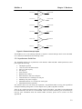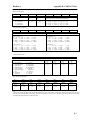
1
BirdBox-A™
C/C++ Programmable, 16-bit Microprocessor Module
Based on the Am188ES
With 4 UARTs, LCD, keypad, and enclosure
Technical
Manual
1724 Picasso Avenue, Suite A, Davis, CA 95616, USA
Tel: 530-758-0180
Fax: 530-758-0181
COPYRIGHT
BirdBox-A, BirdBox-I, BirdBox, A-Engine, A-Engine-P, i386-Engine, NT-Kit, and
ACTF are trademarks of TERN, Inc.
Am188ES and Am186ES are trademarks of Advanced Micro Devices, Inc.
Borland C/C++ is a trademark of Borland International.
Microsoft, MS-DOS, Windows, Windows95, and Windows98 are trademarks of
Microsoft Corporation.
IBM is a trademark of International Business Machines Corporation.
Version 2.00
May 12, 1999
No part of this document may be copied or reproduced in any form or by any means
without the prior written consent of TERN, Inc.
© 1998-1999
1724 Picasso Avenue, Suite A, Davis, CA 95616, USA
Tel: 530-758-0180 Fax: 530-758-0181
Internet Email: [email protected]
http://www.tern.com
Important Notice
TERN is developing complex, high technology integration systems. These systems are
integrated with software and hardware that are not 100% defect free. TERN products are
not designed, intended, authorized, or warranted to be suitable for use in life-support
applications, devices, or systems, or in other critical applications. TERN and the Buyer
agree that TERN will not be liable for incidental or consequential damages arising from
the use of TERN products. It is the Buyer's responsibility to protect life and property
against incidental failure.
TERN reserves the right to make changes and improvements to its products
without providing notice.
BirdBox-A
Table of Contents
Table of Contents
Chapter
page
1. Introduction ................................................. 1-1
1.1 Functional Description .......................... 1-1
1.2 Features ................................................ 1-2
1.3 Physical Description .............................. 1-3
1.4 BirdBox-A Programming Overview ....... 1-4
1.4.1 Step 1 ............................................ 1-5
1.4.1 Step 2 ............................................ 1-6
1.4.1 Step 3 ............................................ 1-6
1.5 Minimum Requirements ............................. 1-6
1.5.1 Minimum Hardware Requirements 1-6
1.5.2 Minimum Software Requirements.. 1-7
2. Installation ................................................... 2-1
2.1 Software Installation ............................. 2-1
2.2 Hardware Installation ............................ 2-1
2.2.1 Connecting the BirdBox-A to
the PC .......................................... 2-1
2.2.2 Powering-on the BirdBox-A........... 2-2
3. Hardware ..................................................... 3-1
3.1 BirdBox-A/Am188ES – Introduction ... 3-1
3.2 Am188ES – Features ........................... 3-1
3.2.1 Clock ............................................ 3-1
3.2.2 External Interrupts and Schmitt
Trigger Input Buffer .................... 3-1
3.2.3 Asynchronous Serial Ports ............. 3-2
3.2.4 Timer Control Unit ........................ 3-3
3.2.5 PWM outputs and PWD................. 3-3
3.2.6 Power-save Mode........................... 3-3
3.3 Am188ES PIO lines............................... 3-4
3.4 I/O Mapped Devices .............................. 3-6
3.4.1 I/O Space ....................................... 3-6
3.4.2 Programmable Peripheral Interface
(PPI, 82C55A).............................. 3-7
3.4.3 Real-time Clock RTC72423 .......... 3-8
3.4.4 UART SCC2691 – Serial Ports ..... 3-8
3.4.5 Parallel Port .................................. 3-9
3.4.6 SER1 MODEM Interface .............. 3-9
3.5 Other Devices ...................................... 3-10
3.5.1 Interrupt Driven Keypad ............. 3-10
3.5.2 LCD Display ............................... 3-11
3.5.3 On-board Supervisor with Watchdog
Timer ......................................... 3-11
Chapter
page
3.5.4 EEPROM .....................................3-11
3.5.5 12-bit ADC (TLC2543) ...............3-12
3.5.6 Dual 12-bit DAC .........................3-12
3.5.7 High Voltage/Current Drivers ......3-13
3.5.8 Switching Power Supply ..............3-14
3.5.9 LED/Beeper .................................3-15
3.6 Headers and Connectors .......................3-15
3.6.1 Expansion Headers J1 and J2........3-15
3.6.2 Jumpers........................................3-17
4. Software ...................................................... 4-1
4.1 AE.LIB / BB.LIB .................................. 4-2
4.2 Functions in AE.OBJ ............................ 4-3
4.2.1 BirdBox-A Initialization ............... 4-3
4.2.2 External Interrupt Initialization .... 4-4
4.2.3 I/O Initialization ........................... 4-5
4.2.4 Timer Units .................................. 4-6
4.2.5 Analog-to-Digital Conversion ....... 4-7
4.2.6 Digital-to-Analog Conversion ....... 4-7
4.2.7 Other Library Functions ............... 4-7
4.3 Functions in BB.LIB ............................. 4-9
4.4 Functions in SER0.OBJ/SER1.OBJ ......4-10
4.5 Functions in SCC.OBJ/SCC1.OBJ .......4-14
4.6 Functions in AEEE.OBJ .......................4-17
Appendices:
A. BirdBox-A Layout.................................A-1
B. UART SCC2691 .................................. B-1
C. RTC72421/72423 .................................C-1
D. Serial EEPROM Map ...........................D-1
E. Software Glossary ................................. E-1
F. Enclosure ............................................. F-1
G. RJ11-DB9 Cable ...................................G-1
Schematics:
BirdBox-A
i
BirdBox-A
Chapter 1: Introduction
Chapter 1: Introduction
1.1 Functional Description
The BirdBox-A (BB-A) is a low-cost universal communication unit. The system supports up to four serial
ports. Two UARTs from the CPU (Am188ES SER0 and SER1) and two optional SCC2691 UARTs are
provided on the BB-A. RS232 drivers are provided for the two CPU UARTs. The SCC2691 UARTs can
be supported separately with either RS232 or RS-485 drivers. All four UARTs have 10-pin headers as
default, or RJ-11/DB9 connectors can optionally be installed (as part of the BB-Pack).
Beeper
Keypad
(Telephone)
LCD
16x2
High
Voltage
Driver
Am188ES
40 MHz
PPI(U5) + PPI(U16)
Print Port
Red
LED
Green
LED
RS232C
SER0
RS232C
SCC2691(U8)
RS232C
SER1
RS232C
SCC2691(U02)
High Voltage Outputs(7)
12-bit ADC(11)
12-bit DAC(2)
RS485
Network
Chain I/O
LCD interface
Figure 1.1 Functional block diagram of BirdBox-A
The two PPIs provide 24x2 bi-directional I/O lines. Eleven digital outputs and five digital inputs connect
to a DB25 connector that can be used as a printer port. The BB-A has seven channels of solenoid drivers
on-board that have the capability to sink up to 350 mA at 50V per channel by default, or an optional eight
channels of sourcing solenoid drivers may be installed instead.
The connectors available with the optional BB-Pack consist of a DB9 connector for the SER1 RS232
serial port, a DB25 connector for a parallel printer port, and RJ11 phone jacks for the SER0 RS232 port
and the two SCC RS232/RS485 UARTs. Offered with these connectors are a 16x2 character LCD, an
interrupt-driven 3x4 keypad, a reset push-button, red and green LEDs, a beeper, and a DC power jack, all
packaged in a 4.80 x 3.72 x 1.5-inch aluminum sheet enclosure.
You may connect the BB-A to computers, control systems, and external MODEMs via the RS-232 serial
ports. You may also connect a printer via the parallel port. The BB-A can be used to convert protocols
into different formats, to check passwords and PIN-code entry, and to translate messages for
communication among different systems or machines. Seven high-voltage drivers, and 11 TTL outputs
and 5 TTL inputs at the DB25 printer port are also available. Up to 250 BirdBox-As may be networked
together via an RS-485 multi-drop system with twisted-pair wires (using the NT-Kit).
1-1
Chapter 1: Introduction
BirdBox-A
1.2 Features
Standard Features
•
•
•
•
•
•
•
•
•
•
•
•
•
•
•
•
•
•
Dimensions: 4.80 x 3.72 x 1.50 inches (with enclosure)
Easy to program in Borland C/C++
Power consumption: 190/130 mA at 5V for 40/20 MHz
Power saving mode: 60/40 mA at 5V for 40/20 MHz
Power input: +8.5V to +35 V unregulated DC, or +5V regulated DC
Temperature range: -40°C to +85°C
16-bit CPU (Am188ES), Intel 80x86 compatible
High performance, zero-wait-state operation at 40 MHz
Up to 512KB Flash/ROM
2 high-speed PWM outputs and Pulse Width Demodulation
32 I/O lines from Am188ES, 512-byte serial EEPROM
8 external interrupt inputs, three 16-bit timer/counters
Two CPU UARTs (RS232)
Supervisor chip (691) for power failure, reset and watchdog
48 additional bi-directional I/O lines from two PPI 82C55
Interface for LCD, keypads, and slave CPU operation
Seven channels of solenoid sinking drivers (default), or eight channels sourcing drivers
Parallel port/printer interface
Optional Features (* surface-mounted components):
•
•
•
•
32KB, 128KB, or 512KB SRAM*
11 channels of 12-bit ADC, sample rate up to 10 KHz*
2 channels of 12-bit DAC, 0-4.095V output*
Two SCC2691 UARTs (on-board) support 8-bit or 9-bit networking
UARTs come with RS232 (default) or 485 drivers
• Real-time clock RTC72423*, lithium coin battery*
BB-Pack:
• 16 characters x 2 lines LCD display
• Beeper, LEDs, interrupt-driven 4 x 3 keypad
• DB25 connector for parallel port
• DB9/RJ11 phone jack connectors for serial ports
• Aluminum sheet metal enclosure
1-2
BirdBox-A
Chapter 1: Introduction
1.3 Physical Description
The physical layout of the BirdBox-A is shown in Figure 1.2.
Highvoltage
Drivers
SER0
RS232
J12
J05
H5
Linear or
switching
regulator
9V to 12V for linear regulator
9V to 35V for switching regulator
(3.6, 4.5)
J11
H4
RS232 /
RS485
U15
High voltage Drivers
Highvoltage
Drivers
H2
RS232
J15
H1
Power jack
RS232/
RS485
for U02
SER1
RS232
U12
PPI (U16)
LCD
PPI
HC259
U16
U02
J8
H10
UART
J4
J5
H8
J3
ROM/
Flash
74HC
14
U3
SRAM
Am188ES
U8
U
A
R
T
U1
U7
EE
U2
DAC U11
PIO pins
from
Am188ES
J1
Data
address
control
bus
U9
Battery
Pot for
LCD
contrast
PPI
Beeper
RTC
J2
ADC
TLC2543
U10
U5
Watchdog
enable
U4
691
ADC
DAC
RS232 /
RS485
H0
J9
U6
Red LED
H13
H13
J6
K1
(0.00, 0.00)
PPI (U5)
Printer Port
Keypad
H3
(free)
Green LED
N2
RS485/
RS232
for U8
Remote
power reset
Reset
Figure 1.2 Physical layout of the BirdBox-A
1-3
Chapter 1: Introduction
BirdBox-A
1.4 BirdBox-A Programming Overview
Development of application software for the BirdBox-A consists of three easy steps, as shown in the block
diagram below.
STEP 1 Serial link PC and BirdBox-A, program in C/C++
Debug C/C++ program on the i386-Drive with Remote Debugger
STEP 2
Test BirdBox-A in the field, away from PC
Application program resides in the battery-backed SRAM
STEP 3
Make application ROM or Download to Flash
Replace DEBUG ROM, project is complete
You can program the BirdBox-A from your PC via serial link with an RS232 interface. Your C/C++
program can be remotely debugged over the serial link at a rate of 115,000 baud. The C/C++ Evaluation
Kit (EV) or Development Kit (DV) from TERN provides a Borland C/C++ compiler, TASM, LOC31,
Turbo Remote Debugger, I/O driver libraries, sample programs, and batch files. These kits also include a
DEBUG ROM (TDREM_AE) to communicate with Turbo Debugger, a PC-V25 cable to connect the
controller to the PC, and a 9-volt wall transformer. See your Evaluation/Development Kit Technical
Manual for more information on these kits.
After you debug your program, you can test run the BirdBox-A in the field, away from the PC, by
changing a single jumper, with the application program residing in the battery-backed SRAM. When the
field test is complete, application ROMs can be produced to replace the DEBUG ROM. The .HEX or .BIN
file can be easily generated with the makefile provided. You may also use the DV Kit or ACTF Kit to
download your application code to on-board Flash.
The three steps in the development of a C/C++ application program are explained in detail below.
1-4
BirdBox-A
Chapter 1: Introduction
1.4.1 Step 1
STEP 1: Debugging
Write your C/C++ application program in C/C++.
Connect your controller to your PC via the PC-V25 serial link cable.
Use the batch file m.bat to compile, link, and locate, or use t.bat to compile, link locate, download,
and debug your C/C++ application program.
RED edge of cable
connects to pin 1
of SER0 (H1)
IDE10
DC
power
jack
To H1
J15
H1
H2
J12
J05
J11
High voltage
U1
H5
H4
RS232
/
DB9
U12
PPI
U1 U01
HC25
U0
J8
U16
UART
J4
J5
PC
RO
M/
U3
U9
To COM1
or COM2
SRA
M
Am188E
S
U
8
U
A
R
T
U1
EE U7
DA U1
C
ADC
J2 TLC25
U1
H1
H8
J3
U2
J1
Wall transformer
+9V 500 mA
center negative
PPI
RTC
U5
U4
691
U1
U1
H0
RS23
2/
H1
J6
K
J9
U6
H1
N2
H3
Figure 1.3 Step 1 connections for the BirdBox-A
1-5
Chapter 1: Introduction
BirdBox-A
1.4.2 Step 2
STEP 2: Standalone Field Test.
Set the jumper on J2 pins 38-40 on the BirdBox-A (Figure 1.4).
At power-on or reset, if J2 pin 38 (P4) is low, the CPU will run the code that resides in the battery-backed
SRAM.
If a jumper is on J2 pins 38-40 at power-on or reset, the BirdBox-A will operate in Step Two mode. If the
jumper is off J2 pins 38-40 at power-on or reset, the BirdBox-A will operate in Step One mode. The status
of J2 pin 38 (signal P4) of the Am188ES is only checked at power-on or at reset.
H1
H2
J12
J05
H4
RS232 /
RS485
High voltage Driver
U15
H5
J11
RS232
J15
U12
PPI
HC259
U16
U02
J8
UART
H10
J4
J5
Step Two Jumper:
H8
J3
ROM/
Flash
74HC
14
U3
SRAM
Am188ES
J1
U8
U9
J2: pins 38=40
U
A
R
T
U1
EE
U7
U2
DAC U11
PPI
RTC
J2
ADC
TLC2543
U10
U5
U4
691
RS232 /
RS485
H0
J9
U6
H13
H13
J6
K1
N2
H3
Figure 1.4 Location of Step Two jumper on the BirdBox-A
1.4.3 Step 3
STEP 3: Generate the application .BIN or .HEX file, make production ROMs or download your program
to FLASH via ACTF.
If you are happy with your Step Two test, you can go back to your PC to generate your application ROM to
replace the DEBUG ROM (TDREM_AE). You need to change DEBUG=1 to DEBUG=0 in the makefile.
You need to have the DV Kit to complete Step Three.
Please refer to the Tutorial of the Technical Manual of the EV/DV Kit for further details on programming
the BirdBox-A.
1.5 Minimum Requirements for BirdBox-A System Development
1.5.1 Minimum Hardware Requirements
•
•
1-6
PC or PC-compatible computer with serial COMx port that supports 115,200 baud
BirdBox-A controller with DEBUG ROM TDREM_AE
BirdBox-A
•
•
Chapter 1: Introduction
PC-V25 serial cable (RS232; DB9 connector for PC COM port and IDC 2x5 connector for controller)
center negative wall transformer (+9V 500 mA)
1.5.2 Minimum Software Requirements
• TERN EV/DV Kit installation diskettes
• PC software environment: DOS, Windows 3.1, Windows95, or Windows98
The C/C++ Evaluation Kit (EV) and C/C++ Development Kit (DV) are available from TERN. The EV
Kit is a limited-functionality version of the DV Kit. With the EV Kit, you can program and debug the
BirdBox-A in Step One and Step Two, but you cannot run Step Three. In order to generate an application
ROM/Flash file, make production version ROMs, and complete the project, you will need the
Development Kit (DV).
1-7
BirdBox-A
Chapter 2: Installation
Chapter 2: Installation
2.1 Software Installation
Please refer to the Technical manual for the “C/C++ Development Kit and Evaluation Kit for TERN
Embedded Microcontrollers” for information on installing software.
The README.TXT file on the TERN EV/DV disk contains important information about the installation
and evaluation of TERN controllers.
2.2 Hardware Installation
Hardware installation for the BirdBox-A consists primarily of connecting the microcontroller to your PC.
Overview
• Connect PC-V25 cable:
For debugging (Step One), place ICD connector on SER0 with red
edge of cable at pin 1
• Connect wall transformer:
Connect 9V wall transformer to power and plug into power jack
2.2.1 Connecting the BirdBox-A to the PC
The following diagram (Figure 2.1) illustrates the connection between the BirdBox-A and the PC. The
BirdBox-A is linked to the PC via a serial cable (PC-V25).
The TDREM_AE DEBUG ROM communicates through SER0 by default. Install the 5x2 IDC connector to
the SER0 header. IMPORTANT: Note that the red side of the cable must point to pin 1 of the H1
header. The DB9 connector should be connected to one of your PC's COM Ports (COM1 or COM2).
power jack
RED side of serial
cable corresponding
to pin 1 of headers for
SER0/SER1
To SER0
for debugging
PP1
ROM
U A R T
691
SRAM
To COM1
or COM2
PP1
Am188ES
RTC
EE
ADC
PC
IDC
connector
9-pin
connector
Pin 1 of
SER0
BirdBox-A
Figure 2.1 Connecting the BirdBox-A to the PC
2-1
Chapter 2: Installation
BirdBox-A
2.2.2 Powering-on the BirdBox-A
Connect a wall transformer +9V DC output to the DC power jack at H4.
The red on-board LED (located on the bottom side of the board) should blink twice and remain on after
the BirdBox-A is powered-on or reset (Figure 2.2).
Wall
transformer
H1
H2
J12
J05
H4
Power
jack
RS232 /
RS485
High voltage Driver
U15
H5
J11
RS232
J15
U12
PPI
HC259
U16
U02
J8
H10
UART
J4
J5
H8
J3
ROM/
Flash
74HC
14
U3
SRAM
Am188ES
J1
U8
U9
U
A
R
T
U1
EE
U7
DAC
U11
U2
PPI
RTC
J2
ADC
TLC2543
U10
U5
U4
691
RS232 /
RS485
H0
J9
U6
H13
J6
H13
K1
N2
H3
Red
LED
Figure 2.2 The red LED blinks twice after the BirdBox-A is powered-on or reset
2-2
BirdBox-A
Chapter 3: Hardware
Chapter 3: Hardware
3.1 Birdbox-A/Am188ES – Introduction
The BirdBox-A is based on a combination of the A-Engine and BirdBox designs, and combines the best
features of both. It is based on Am188ES processor architecture.
The Am188ES is based on the industry-standard x86 architecture. The Am188ES controllers are higherperformance, more integrated versions of the 80C188 microprocessors. In addition, the Am188ES has
new peripherals. The on-chip system interface logic can minimize total system cost. The Am188ES has
two asynchronous serial ports, 32 PIOs, a watchdog timer, additional interrupt pins, a pulse width
demodulation option, DMA to and from serial ports, a 16-bit reset configuration register, and enhanced
chip-select functionality.
3.2 Am188ES – Features
3.2.1 Clock
Due to its integrated clock generation circuitry, the Am188ES microcontroller allows the use of a timesone crystal frequency. The design achieves 40 MHz CPU operation, while using a 40 MHz crystal.
The system CLKOUTA signal is routed to J1 pin 23, default 40 MHz. The CLKOUTB signal is not
connected in the BirdBox-A.
CLKOUTA remains active during reset and bus hold conditions. The initialization function ae_init();
disables CLKOUTA and CLKOUTB with clka_en(0).
You can use clka_en(1) to enable the signal CLKOUTA=CLK at header J1 pin 23.
3.2.2 External Interrupts and Schmitt Trigger Input Buffer
There are eight external interrupts: INT0-INT6 and NMI.
/INT0, J2 pin 8, is used by the UART (SCC2691, U8), if it is installed.
/INT1, J2 pin 6, is used by the other optional UART (SCC2691, U02).
/INT2, J2 pin 19
/INT3, J2 pin 21
/INT4, J2 pin 33
INT5=P12=DRQ0, J2 pin 5, used by BirdBox-A as output for LED/EE/HWD
INT6=P13=DRQ1, J2 pin 11
/NMI, J2 pin 7
Six of these external interrupt inputs, /INT0-4 and /NMI, are buffered by Schmitt-trigger inverters (U9),
in order to increase noise immunity and transform slowly changing input signals to fast changing and
jitter-free signals. As a result of this buffering, these pins are capable of only acting as input.
3-1
BirdBox-A
Chapter 3: Hardware
INT4 =U2.52
/INT4=J2.33
U9A
INT2 =U2.54
/INT2=J2.19
U9B
INT0 =U2.56
/INT0=J2.8
U9C
/INT1=J2.6
INT1=U2.55
U9D
INT3=U2.53
/INT3=J2.21
U9E
/NMI=J2.7
NMI=U2.47
U9F
Figure 3.1 External interrupt inputs
The BirdBox-A uses vector interrupt functions to respond to external interrupts. Refer to the Am188ES
User’s manual for information about interrupt vectors.
3.2.3 Asynchronous Serial Ports
The Am188ES CPU has two asynchronous serial channels: SER0 and SER1. Both asynchronous serial
ports support the following:
• Full-duplex operation
• 7-bit, 8-bit, and 9-bit data transfers
• Odd, even, and no parity
• One stop bit
• Error detection
• Hardware flow control
• DMA transfers to and from serial ports
• Transmit and receive interrupts for each port
• Multidrop 9-bit protocol support
• Maximum baud rate of 1/16 of the CPU clock speed
• Independent baud rate generators
The software drivers for each serial port implement a ring-buffered DMA receiving and ring-buffered
interrupt transmitting arrangement. See the samples files s1_echo.c, s0_echo.c for details.
There are two optional external SCC2691 UARTs located on the BB-A. One (U8) is located underneath
the U3 ROM socket. The other is at location U02. There are software interfaces given for interfacing to
both For more information about the external UART SCC2691, please refer to section 3.4.4 and
Appendix B.
3-2
BirdBox-A
Chapter 3: Hardware
3.2.4 Timer Control Unit
The timer/counter unit has three 16-bit programmable timers: Timer0, Timer1, and Timer2.
Timer0 and Timer1 are connected to four external pins:
Timer0 output = P10 = J2 pin 12
Timer0 input = P11 = J2 pin 14
Timer1 output = P1 = J2 pin 29 = J1 pin 4
Timer1 input = P0 = J2 pin 20
These two timers can be used to count or time external events, or they can generate non-repetitive or
variable-duty-cycle waveforms.
Timer2 is not connected to any external pin. It can be used as an internal timer for real-time coding or
time-delay applications. It can also prescale timer 0 and timer 1 or be used as a DMA request source.
The maximum rate at which each timer can operate is 10 MHz, since each timer is serviced once every
fourth clock cycle. Timer output takes up to six clock cycles to respond to clock or gate events. See the
sample programs timer0.c and ae_cnt0.c in the \samples\ae directory.
3.2.5 PWM outputs and PWD
The Timer0 and Timer1 outputs can also be used to generate non-repetitive or variable-duty-cycle
waveforms. The timer output takes up to 6 clock cycles to respond to the clock input. Thus the minimum
timer output cycle is 25 ns x 6 = 150 ns (at 40 MHz).
Each timer has a maximum count register that defines the maximum value the timer will reach. Both
Timer0 and Timer1 have secondary maximum count registers for variable duty cycle output. Using both
the primary and secondary maximum count registers lets the timer alternate between two maximum
values.
MAX. COUNT A
MAX. COUNT B
Pulse Width Demodulation can be used to measure the input signal’s high and low phases on the
/INT2=J2 pin 19.
3.2.6 Power-save Mode
The power-save mode of the Am188ES reduces power consumption and heat dissipation, thereby
extending battery life in portable systems. In power-save mode, operation of the CPU and internal
peripherals continues at a slower clock frequency. When an interrupt occurs, it automatically returns to its
normal operating frequency.
The RTC72423 on the BirdBox-A has a VOFF signal routed to J1 pin 9. VOFF is controlled by the
battery-backed RTC72423. The VOFF signal can be programmed by software to be in tri-state or to be
active low. The RTC72423 can be programmed in interrupt mode to drive the VOFF pin at 1/64 second, 1
second 1 minute, or 1 hour intervals. The user can use the VOFF line to control the external switching
power supply that turns the power supply on/off. More details are available in the sample file poweroff.c
in the 186\samples\ae sub-directory.
3-3
BirdBox-A
Chapter 3: Hardware
3.3 Am188ES PIO lines
The Am188ES has 32 pins available as user-programmable I/O lines. Each of these pins can be used as a
user-programmable input or output signal, if the normal shared function is not needed. A PIO line can be
configured to operate as an input or output with or without a weak pull-up or pull-down, or as an opendrain output. A pin’s behavior, either pull-up or pull-down, is pre-determined and shown in the table
below.
After power-on/reset, PIO pins default to various configurations. The initialization routine provided by
TERN libraries reconfigures some of these pins as needed for specific on-board usage as well. These
configurations, as well as the processor-internal peripheral usage configurations, are listed below in Table
3.1.
PI
O
Function
Power-On/Reset status
BirdBox-A Pin No.
BirdBox-A Initial
P0
P1
P2
P3
P4
P5
P6
P7
P8
P9
P10
P11
P12
P13
P14
P15
P16
P17
P18
P19
P20
P21
P22
P23
P24
P25
P26
P27
P28
P29
P30
P31
Timer1 in
Timer1 out
/PCS6/A2
/PCS5/A1
DT/R
/DEN/DS
SRDY
A17
A18
A19
Timer0 out
Timer0 in
DRQ0/INT5
DRQ1/INT6
/MCS0
/MCS1
/PCS0
/PCS1
CTS1/PCS2
RTS1/PCS3
RTS0
CTS0
TxD0
RxD0
/MCS2
/MCS3
UZI
TxD1
RxD1
/CLKDIV2
INT4
INT2
Input with pull-up
Input with pull-down
Input with pull-up
Input with pull-up
Normal
Normal
Normal
Normal
Normal
Normal
Input with pull-down
Input with pull-up
Input with pull-up
Input with pull-up
Input with pull-up
Input with pull-up
Input with pull-up
Input with pull-up
Input with pull-up
Input with pull-up
Input with pull-up
Input with pull-up
Input with pull-up
Input with pull-up
Input with pull-up
Input with pull-up
Input with pull-up
Input with pull-up
Input with pull-up
Input with pull-up
Input with pull-up
Input with pull-up
J2 pin 20
J2 pin 29, J1 pin 16
J2 pin 24
J2 pin 15
J2 pin 38
J2 pin 30
J2 pin 35
J8 pin 3
J8 pin 2
J8 pin 1
J2 pin 12
J2 pin 14
J2 pin 5
J2 pin 11
J2 pin 37
J2 pin 23
J1 pin 19
J2 pin 13
J2 pin 22
J2 pin 31
J2 pin 27
J2 pin 36
J2 pin 34
J2 pin 32
J2 pin 17
J2 pin 18
J2 pin 4
J2 pin 28
J2 pin 26
J2 pin 3
J2 pin 33
J2 pin 19
Input with pull-up
CLK_1
RTC select
SCC2691 (U8) select
Input with pull-up Step 2
Input with pull-up
Input with pull-down
A17
A18
A19
Input with pull-down
Input with pull-up
Output for LED/EE/HWD
Input with pull-up
Input with pull-up
Input with pull-up
PPI (82C55,U16) chip select
PPI (82C55,U5) chip select
Input with pull-up
Input with pull-up
Input with pull-up
Input with pull-up
TxD0
RxD0
Input with pull-up
Input with pull-up
Input with pull-up*
TxD1
RxD1
Input with pull-up*
Input with pull-up
Input with pull-up
* Note: P26, P29 must NOT be forced low during power-on or reset.
Table 3.1 I/O pin default configuration after power-on or reset
Three external interrupt lines are not shared with PIO pins:
INT0 = J2 pin 2
3-4
BirdBox-A
Chapter 3: Hardware
INT1 = J2 pin 6
INT3 = J2 pin 21
The 32 PIO lines, P0-P31, are configurable via two 16-bit registers, PIOMODE and PIODIRECTION.
The settings are as follows:
MODE
0
1
2
3
PIOMODE reg.
0
0
1
1
PIODIRECTION reg.
0
1
0
1
PIN FUNCTION
Normal operation
INPUT with pull-up/pull-down
OUTPUT
INPUT without pull-up/pull-down
BirdBox-A initialization on PIO pins in ae_init() is listed below:
outport(0xff78,0xe73c);
// PDIR1, TxD0, RxD0, TxD1, RxD1, P16=PCS0, P17=PCS1=PPI
outport(0xff76,0x0000);
// PIOM1
outport(0xff72,0xec7b);
// PDIR0, P12,A19,A18,A17,P2=PCS6=RTC
outport(0xff70,0x1000);
// PIOM0, P12=LED
The C function in the library ae_lib can be used to initialize PIO pins.
void pio_init(char bit, char mode);
Where bit = 0-31 and mode = 0-3, see the table above.
Example:
pio_init(12, 2); will set P12 as output
pio_init(1, 0); will set P1 as Timer1 output
void pio_wr(char bit, char dat);
pio_wr(12,1); set P12 pin high, if P12 is in output mode
pio_wr(12,0); set P12 pin low, if P12 is in output mode
unsigned int pio_rd(char port);
pio_rd (0); return 16-bit status of P0-P15, if corresponding pin is in input mode,
pio_rd (1); return 16-bit status of P16-P31, if corresponding pin is in input mode,
Some of the I/O lines are used by the BirdBox-A system for on-board components (Table 3.2). We
suggest that you not use these lines unless you are sure that you are not interfering with the operation of
such components (i.e., if the component is not installed).
You should also note that the external interrupt PIO pins INT2, 4, 5, and 6 are not available for use as
output because of the inverters attached. The input values of these PIO interrupt lines will also be
inverted for the same reason. As a result, calling pio_rd to read the value of P31 (INT2) will return 1
when pin 19 on header J2 is pulled low, with the result reversed if the pin is pulled high.
Signal
P2
P3
P4
P11
Pin
/PCS6
/PCS5
/DT
Timer0 input
P12
P16
P17
P18
DRQ0/INT5
/PCS0
/PCS1
/CTS1/PCS2
Function
U4 RTC72423 chip select at base I/O address 0x0600
U8 SCC2691 UART chip select at base I/O address 0x0500
STEP 2 jumper
Shared with U19 TLC2543 ADC and U7 24C04 EE data input
The ADC and EE data output can be tri-state, while disabled
Output for LED or U7 serial EE clock or Hit watchdog
U16 PPI chip select at base I/O address 0x0000 (LCD Header)
U5 PPI chip select at base I/O address 0x0100 (Parallel Port)
U02 SCC2691 UART chip select at base I/O address 0x0200
3-5
BirdBox-A
Signal
P19
P22
P23
INT0
INT1
Chapter 3: Hardware
Pin
/RTS1/PCS3
TxD0
RxD0
J2 pin 2
J2 pin 6
Function
U18 Latch at base I/O address 0x0300 (High Voltage Outputs)
Default SER0 debug
Default SER0 debug
U8 SCC2691 UART interrupt.
U02 SCC2691 UART interrupt
Table 3.2 I/O lines used for on-board components
3.4 I/O Mapped Devices
3.4.1 I/O Space
External I/O devices can use I/O mapping for access. You can access such I/O devices with inportb(port)
or outportb(port,dat). These functions will transfer one byte or word of data to the specified I/O address.
The external I/O space is 64K, ranging from 0x0000 to 0xffff.
The default I/O access time is 15 wait states. You may use the function void io_wait(char wait) to define
the I/O wait states from 0 to 15. The system clock is 25 ns ( or 50 ns), giving a clock speed of 40 MHz (or
20 MHz). Details regarding this can be found in the Software chapter, and in the Am188ES User’s
Manual. Slower components, such as most LCD interfaces, might find the maximum programmable wait
state of 15 cycles still insufficient. Due to the high bus speed of the system, some components need to be
attached to I/O pins directly.
For details regarding the chip select unit, please see Chapter 5 of the Am188ES User’s Manual.
The table below shows more information about I/O mapping.
I/O space
0x0000-0x00ff
0x0100-0x01ff
0x0200-0x02ff
Select
/PCS0
/PCS1
/PCS2
0x0300-0x03ff
/PCS3
0x0400-0x04ff
0x0500-0x05ff
0x0600-0x06ff
/PCS4
/PCS5
/PCS6
Location
J1 pin 19=P16
J2 pin 13=P17
J2
pin
22=CTS1
J2
pin
31=RTS1
J2 pin 15=P3
J2 pin 24=P2
Usage
PPI (U16)
PPI (U5)
UART (U02)
74HC259 (U18)
Reserved
UART (U8)
RTC 72423
Some of the above chip select lines are free for use if optional components are not installed. This includes
/PCS2, /PCS5, and /PCS6.
In applications where the high voltage output (HV0-HV7) is not used, the latch U18 is not necessary.
That allows chip select line /PCS3 to be used for any user application as well.
To illustrate how to interface the BirdBox-A with external I/O boards, a simple decoding circuit for
interfacing to a 82C55 parallel I/O chip is shown below in Figure 3.2.
3-6
BirdBox-A
Chapter 3: Hardware
82C55
74HC138
A5
A6
A7
1
2
3
A
B
C
4
5
6
/PCS3
VCC
Y0
Y1
Y2
Y3
Y4
Y5
Y6
Y7
G2A
G2B
G1
RST
A0
A1
NC
/SEL20
/SEL40
/SEL60
/SEL80
/SELA0
/SELC0
/SELF0
15
14
13
12
11
10
9
7
P00-P07
/SEL20
/CS
P10-P17
/WR
/WR
/RD
/RD
P20-P27
D0-D7
Figure 3.2 Interface the BirdBox-A to external I/O devices
The function ae_init() by default initializes the /PCS3 line at base I/O address starting at 0x300. You
can read from the 82C55 with inportb(0x320) or write to the 82C55 with outportb(0x320,dat). The call
to inportb(0x320) will activate /PCS3, as well as putting the address 0x320 over the address bus. The
decoder will select the 82C55 based on address lines A5-7, and the data bus will be used to read the
appropriate data from the off-board component.
3.4.2 Programmable Peripheral Interface (PPI, 82C55A)
The PPI (82C55) is a low-power CMOS programmable parallel interface unit for use in microcomputer
systems. It provides 24 I/O pins that may be individually programmed in two groups of 12 and used in
three major modes of operation.
7
6
5
4
3
2
1
0
GROUP 1
Port 2
(Lower)
Output
0
Port 1
Mode
1
Input
0
Output
1
Input
0
Mode 0
1
Mode 1
GROUP 2
Port 2
(Upper)
Output
0
1
Input
Port 0
0
Output
1
Input
Mode
00
Mode 0
01
Mode 1
1X
Mode 2
Command
Select
0
1
B it
manipulation
Mode
Select
Figure 3.3 Mode Select Command Word
In MODE 0, the two groups of 12 pins can be programmed in sets of 4 and 8 pins to be inputs or outputs.
In MODE 1, each of the two groups of 12 pins can be programmed to have 8 lines of input or output. Of
the 4 remaining pins, 3 are used for handshaking and interrupt control signals. MODE 2 is a strobed bidirectional bus configuration. For most applications, and in almost all TERN sample files, MODE 0 is
3-7
BirdBox-A
Chapter 3: Hardware
the appropriate setting for the PPI ports. That gives you the maximum number of additional digital I/O
pins.
There are two separate PPIs available on the BirdBox-A. The first PPI, U16, is mapped at base I/O
address 0x0000, and supports the LCD via header H10. The second PPI, U5, is mapped to address
0x0100 and drives the parallel/printer port J6.
The ports/registers are offsets of this I/O base address.
The Command Register = 0x0?03; Port 0 = 0x0?00; Port 1 = 0x0?01; and Port 2 = 0x0?02 (where the ‘?’
refers to the appropriate I/O address, based on the PPI being used).
The following code example will set all ports to output mode on the PPI U5:
outportb(0x0103,0x80); /*
outportb(0x0100,0x55); /*
outportb(0x0101,0x55); /*
outportb(0x0102,0x55); /*
Mode
Sets
Sets
Sets
To set all ports to input mode:
outportb(0x0103,0x9f);
0 all output selection. */
port 0 to alternating high/low I/O pins. */
port 1 to alternating high/low I/O pins. */
port 2 to alternating high/low I/O pins. */
/* Mode 0 all input selection. */
You can read the ports with:
inportb(0x0100); /* Port 0 */
inportb(0x0101); /* Port 1 */
inportb(0x0102); /* Port 2 */
This returns a 8-bit value for each port, with each bit corresponding to the appropriate line on the port.
You will find that numerous on-board components are controlled using PPI lines only. You will need to
use PPI access methods to control these, as well.
3.4.3 Real-time Clock RTC72423
If installed, a real-time clock RTC72423 (EPSON, U4) is mapped in the I/O address space at 0x0600. It
must be backed up with a lithium coin battery. The RTC is accessed via software drivers rtc_init() or
rtc_rd() (see Appendix C and the Software chapter for details).
It is also possible to configure the real-time clock to raise an output line attached to an external interrupt,
at 1/64 second, 1 second, 1 minute, or 1 hour intervals. This can be used in a time-driven application, or
the VOFF signal can be used to turn on/off the controller using the switching power supply. Details
regarding the switching power supply can be found in section 3.5.8. An example of a program showing a
similar application can be found in tern\v25\samples\ve\poweroff.c.
3.4.4 UART SCC2691 – Serial Ports
There are two UART SCC2691s (Signetics, U8/U02) mapped into the I/O address space. The first, U8 is
mapped into I/O space at 0x0500. The second UART is mapped into I/O space at 0x0200. Software
interfaces for both are provided and are described in the Software chapter.
The SCC2691 has a full-duplex asynchronous receiver/transmitter, a quadruple buffered receiver data
register, an interrupt control mechanism, programmable data format, selectable baud rate for the receiver
and transmitter, a multi-functional and programmable 16-bit counter/timer, an on-chip crystal oscillator,
and a multi-purpose input/output including RTS and CTS mechanism. MPO and MPI are routed to J1 pin
3 and J1 pin 21. For more detailed technical specifications, refer to Appendix B. U8 may be used as a
network 9-bit UART (for the TERN NT-Kit).
RxD (J1 pin 5), TxD (J1 pin 7), MPO (J1 pin 3), and MPI (J1 pin 21) are TTL level signals for the first
SCC2691 serial port (U8). The second SCC2691 serial port (U02) uses signal pins RxD2, TxD2, CTS2,
and RTS2, which are on header J11. RS-232 and RS-485 drivers are provided to bring the UART serial
3-8
BirdBox-A
Chapter 3: Hardware
outputs to RS-232 or RS-485 signal levels. Both of the SCC UARTs can be configured for either RS232
or RS485 operation.
Two serial ports, SER0 and SER1, are internal to the Am188ES processor. These are both configured for
RS-232 operation on the BirdBox-A as well. Below is a functional diagram of all of the serial ports
available on this unit.
SCC2691
SCC U8
I/O Addr = 0x0500
TxD
/CTS (485-)
RxD
RS232C/RS485 /RTS (485+)
Driver
/TxD
/RxD
MPI
MPO
RTS0
SER0
TxD0
/TxD0
RxD0
/RxD0
CTS0
Am188ES CPU
SCC2691
SCC2 U02
I/O Addr = 0x0200
H3 HDRD10
J3 HDRD10
J12 RJ11 6-6
RS232C
TxD1
SER1
N2 RJ11 6-6
Drivers
RxD1
TxD2
RxD2
RS232C/RS485
Driver
/TxD1
/RxD1
CTS1
J10 HDRD10
RTS1
J5 DB9
/TxD2
/RxD2
MPI2
/RTS2(485+)
MPO2
/CTS2(485-)
H03 HDRD10
J11 RJ11 6-6
BirdBox-A
The default connector configuration for the serial ports is 5x2 pin headers for each, as shown in the
functional diagram above. As part of the BirdBox-A Package (BB-Pack), these headers are replaced with
three optional RJ-11 phone jacks and a DB9 connector.
3.4.5 Parallel Port
A DB25 pin-compatible parallel port is provided at J6. It is configured using standard I/O pins.
The I/O pins on this parallel port are mapped to a PPI (U5) at address 0x100. This parallel port can be
used for general purpose I/O.
A printer driver is also provided to interface to most dot matrix printers, in the sample file
samples/bb/bba_prt.c. If you have detailed specifications for your printer, you can create your own
parallel port driver.
3.4.6 SER1 MODEM Interface
The SER1 serial channel of the BirdBox has two connectors: one is J10, and the other, J5 (a DB9
connector), is configured as a DTE device. This connector is compatible with a PC-AT DB9 serial port.
A cable connecting the DB9 connector of the BirdBox-A to the DB25 connector of an external MODEM
(RS232C) can be constructed as shown in Figure 3.4.
3-9
BirdBox-A
Chapter 3: Hardware
MODEM RS232C
DB25 1
BirdBox
J5 DB9
TxD
RxD
2
14
3
4
1
2
3
6
5
RTS
CTS
7
8
7
4
5
20
9
GND
DTR
25
13
WANG 9648/24e Data Fax Modem
Figure 3.4 Connection between BirdBox-A J5 DB9 and MODEM RS232C DB25
3.5 Other Devices
A number of other devices are also available on the BirdBox-A. Some of these are optional, and might not
be installed on the particular controller you are using. For a discussion regarding the software interface
for these components, please see the Software chapter.
3.5.1 Interrupt Driven Keypad
A telephone keypad (3x4) is provided as part of the optional BB-Pack for user inputs. As part of the
package, the keypad fits into the metal box enclosure provided for the BirdBox.
The keypad matrix is shown below. Three output lines are used for each of the columns, and four inputs
are provided to read values from each row of the keypad.
vcc
1
2
3
4
5
6
7
8
9
*
0
#
COL1= I16
COL2= I17
ROW1= P23
vcc
ROW2= I20
vcc
ROW3= I21
vcc
ROW4= I22
COL3= I15
3-10
BirdBox-A
Chapter 3: Hardware
By pulling one of the column output pins low, the resulting input row pin for the pressed key will be set
low as well. By reading these input pin values, you can decode the value of the pressed key.
The keypad is interfaced at header K1, and the signals are all from the PPI (U5) I/O pins.
The keypad can also be used to generate external interrupts. Choose one of the keys to be used as your
“interrupt” key. By pulling its column low, its row input can be connected to one of the active-low
external interrupts and will raise an interrupt if the key is ever pressed.
For a sample program showing how to read and decode the signals from the keypad, please see the sample
file bba_kpad.c.
3.5.2 LCD Display
A 16x2 alphanumeric character-based LCD is also available as part of the BirdBox-A Package. It is
connected to header H10, and uses PPI (U16) I/O pins to drive the LCD. Pins 5 through 18 on the header
are used to connect to the LCD. The LCD is mounted on the back side of the board. If you have
purchased an LCD, pin 8 on this header is disconnected from PPI signal B12 and connected to a
potentiometer (pot) for adjustable contrast.
This default LCD fits inside the metal enclosure provided as part of the BB-Pack. Larger LCDs, such as
the 20x4, are also available, but require a different metal enclosure. For details regarding the metal
enclosure, please see Appendix F.
The LCD display also has a detailed sample file, bba_lcd.c, demonstrating its use, which provides
documentation for basic write functions to the LCD. If this is insufficient for your application, you can
also find standard technical documentation from Hantronix, Inc. (http://www.hantronix.com, 408-2521100) for your specific LCD module.
3.5.3 On-board Supervisor with Watchdog Timer
The MAX691/LTC691 (U6) is a supervisor chip. With it installed, the BirdBox-A has several functions:
watchdog timer, battery backup, power-on-reset delay, power-supply monitoring, and power-failure
warning. These will significantly improve system reliability.
Watchdog Timer
The watchdog timer is activated by setting a jumper on J9 of the BirdBox-A. The watchdog timer
provides a means of verifying proper software execution. In the user's application program, calls to the
function hitwd() (a routine that toggles the P12=HWD pin of the MAX691) should be arranged such that
the HWD pin is accessed at least once every 1.6 seconds. If the J9 jumper is on and the HWD pin is not
accessed within this time-out period, the watchdog timer pulls the WDO pin low, which asserts /RESET.
This automatic assertion of /RESET may recover the application program if something is wrong. After the
BirdBox-A is reset, the WDO remains low until a transition occurs at the WDI pin of the MAX691. When
controllers are shipped from the factory the J9 jumper is off, which disables the watchdog timer.
The Am188ES has an internal watchdog timer. This is disabled by default with ae_init().
Battery Backup Protection
The backup battery protection protects data stored in the SRAM and RTC. The battery-switch-over circuit
compares VCC to VBAT (+3 V lithium battery positive pin), and connects whichever is higher to the
VRAM (power for SRAM and RTC), backing up the SRAM and the real-time clock RTC72423. In
normal use, the lithium battery should last about 3-5 years without external power being supplied. When
the external power is on, the battery-switch-over circuit will select the VCC to connect to the VRAM.
3-11
BirdBox-A
Chapter 3: Hardware
3.5.4 EEPROM
A 512-byte serial EEPROM (24C04) is installed in U7. The BirdBox-A uses the P12=SCL (serial clock)
and P11=SDA (serial data) to interface with the EEPROM. The EEPROM can be used to store important
data such as a node address, calibration coefficients, and configuration codes. It typically has 1,000,000
erase/write cycles. The data retention is more than 40 years. EEPROM can be read and written by simply
calling the functions ee_rd() and ee_wr().
A range of lower addresses in the EEPROM is reserved for TERN use. Details regarding which addresses
are reserved, and for what purpose, can be found in Appendix D of this manual.
3.5.5 12-bit ADC (TLC2543)
The TLC2543 is a 12-bit, switched-capacitor, successive-approximation, 11 channels, serial interface,
analog-to-digital converter. Three PPI I/O lines from U5 are used to handle the ADC, with /CS=I20;
CLK=I22; and DIN=I21.
The ADC digital data output communicates with a host through a serial tri-state output (DOUT=P11). If
I20=/CS is low, the TLC2543 will have output on P11. If I20=/CS is high, the TLC2543 is disabled and
P11 is free. I20 and P11 are pulled high by 10K resistors on board. The TLC2543 has an on-chip 14channel multiplexer that can select any one of 11 inputs or any one of three internal self-test voltages. The
sample-and-hold function is automatic. At the end of conversion, the end-of-conversion (EOC) output is
not connected, although it goes high to indicate that conversion is complete.
TLC2543 features differential high-impedance inputs that facilitate ratiometric conversion, scaling, and
isolation of analog circuitry from logic and supply noise. A switched-capacitor design allows low-error
conversion over the full operating temperature range. The analog input signal source impedance should be
less than 50Ω and capable of slewing the analog input voltage into a 60 pf capacitor.
A reference voltage less than VCC (+5V) can be provided for the TLC2543 if additional precision is
required. A voltage above 2.5V and less than +5V can be used for this purpose, and can be connected to
the REF+ pin.
The CLK signal to the ADC is toggled through an I/O pin, and serial access allows a conversion rate of up
to approximately 10 KHz.
In order to operate the TLC2543, five I/O lines are used, as listed below:
/CS
DIN
DOUT
EOC
CLK
REF+
REFVCC
GND
Chip select = PPI I20, high to low transition enables DOUT, DIN and CLK.
Low to high transition disables DOUT, DIN and CLK.
PPI I21, serial data input
P11 of Am188ES, 3-state serial data output.
Not Connected, End of Conversion, high indicates conversion complete and
data is ready
I/O clock = PPI I22
Upper reference voltage (normally VCC)
Lower reference voltage (normally GND)
Power supply, +5 V input
Ground
The analog inputs AD0 to AD10, REF+, GND, and VCC are available at H0. The inputs AD7 to AD10
are also available at the DB25 connector J6.
3.5.6 Dual 12-bit DAC
The LTC1446/LTC1446L is a dual 12-bit digital-to-analog converter (DAC) in an SO-8 package. It is
complete with a rail-to-rail voltage output amplifier, an internal reference and a 3-wire serial interface.
3-12
BirdBox-A
Chapter 3: Hardware
The LTC1446 outputs a full-scale of 4.096V, making 1 LSB equal to 1 mV. The LTC1446L outputs a
full-scale of 2.5 V, making 1 LSB equal to 0.61 mV.
The buffered outputs can source or sink 5 mA. The outputs swing to within a few millivolts of supply rail
when unloaded. They have an equivalent output resistance of 40 Ω when driving a load to the rails. The
buffer amplifiers can drive 1000 pf without going into oscillation.
The DAC is installed in U11 on the BirdBox-A, and the outputs are routed to J6 pin 20 for DAC channel
A, and J6 pin 19 for DAC channel B.
The DAC uses P12 as CLK, P26 as DI and P29 as LD/CS. Please refer to the LT1446 technical data
sheets from Linear Technology (1-408-432-1900) for further information. See also the sample program
ae_da.c in the \samples\ae directory.
3.5.7 High Voltage/Current Drivers
The high voltage drivers on the BirdBox-A can be configured for either sourcing or sinking operation.
Two different components are used to provide these operations, and must be specified when ordering. The
sinking driver ULN2003 provides seven channels of sinking output, while the UDS2982 provides eight
channels of sourcing output.
Installed by default, the sinking driver ULN2003 (U15) has high voltage, high current Darlington
transistor arrays, consisting of seven silicon NPN Darlington pairs on a common monolithic substrate. All
channels feature open-collector outputs for sinking 350 mA at 50V, and integral protection diodes for
driving inductive loads. Peak inrush currents of up to 600 mA sinking are allowed.
These outputs may be paralleled to achieve high-load capability, although each driver has a maximum
continuous collector current rating of 350 mA at 50V. The maximum power dissipation allowed is 2.20 W
per chip at 25 degrees Celsius (°C). In this configuration, pin 9 must be connected to ground for the
current to return. This can be done by using a jumper to connect pins 1 (VS) and 3 (GND) on header H6.
If you are expecting to sink a large amount of current, you will have to connect this ground signal to an
external ground using a heavy gauge (20) wire. GK connects to the protection diodes in the ULN2003
chip and should be tied to highest voltage in the external load system. GK can be connected to an
unregulated on-board +12VI signal by connecting H6 pins 2 and 4 by jumper. ULN2003 is a sinking
driver, not a sourcing driver. An example of typical application wiring is shown below.
3-13
BirdBox-A
Chapter 3: Hardware
O1
Solenoid
+12V
Power Supply
GND/SUB
J6 or J7
ULN2003 Birdbox-A
K
+12V
GND/SUB
Figure 3.5 Drive inductive load with high voltage/current drives (ULN2003)
The UDS2982 (technical specifications available from http://www.allegromicro.com) can be installed to
act as a sourcing driver, providing eight channels. It has an output current of up to 500 mA with a load
supply voltage up to 50V. Typical loads for this component include relays, solenoids, lamps, stepper
and/or servo motors, print hammers, and LEDs. The UDS2982 also integrates input current limiting
resistors and output transient suppression diodes.
When the UDS2982 is used, the signal VS must be connected to the load supply voltage. This can be
done by jumper-connecting pins 1 and 2 on header H6 to connect VS to the +12V input voltage. GK acts
as ground, and should be connected using pins 3 and 4 on header H6.
The high voltage drivers have outputs at header H5, and HV1-HV4 are also available at RJ11 jack J15.
3.5.8 Switching Power Supply
A switching power supply voltage regulator (LM2575) is on-board to provide +5V regulated power. The
input voltage provided to the voltage regulator from the signal +12VI should be in the range of 8.5V to
35V. This component has high efficiency, and dramatically reduces excess heat produced on the voltage
regulator.
The VOFF pin on the switching power supply can also be used to power on/off the controller. This is
particularly useful in battery-powered applications where power consumption is especially sensitive, and
the controller can be powered-off for long periods of time. In this mode, power consumption is reduced to
3 µA. When this pin is pulled high, the voltage regulator will power down the controller. You can pull
this pin low manually by using a jumper to connect header H7. If this pin is instead connected to another
source, such as an external digital signal or the real-time-clock, the controller can be turned on/off
automatically.
The unregulated voltage supply can be connected to header H4.
If you have a regulated 5V voltage supply source, it can be connected to any of the VCC/GND pins on
headers J1 and J2.
3-14
BirdBox-A
Chapter 3: Hardware
3.5.9 LED/Beeper
An optional beeper (provided as part of the BB-Pack) is available connected to PIO line P26. Oscillating
this pin high and low will cause the beeper to sound. A sample file showing its use, bba_beep.c, is found
in 186\samples\bb.
Two LEDs, one green and one red, are also available on the BirdBox-A. These are turned on using lines
P26 and P12, respectively. Pulling either low will turn the corresponding LED on.
3.6 Headers and Connectors
3.6.1 Expansion Headers J1 and J2
There are two 20x2 0.1 spacing headers for BirdBox-A expansion. Most signals are directly routed to the
Am188ES processor. These signals are 5V only, and any out-of-range voltages will most likely damage
the board.
(3.6, 4.5)
H2
J12
J05
RS232 /
RS485
H5
High voltage Driver
U15
H4
J11
RS232
J15
H1
U12
PPI
HC259
U16
U02
J8
H10
UART
J4
J5
H8
J3
ROM/
Flash
74HC
14
U3
SRAM
Am188ES
J1
J1 pin 1
U8
U9
U
A
R
T
U1
J2 pin 1
EE
U7
DAC
U11
U2
PPI
RTC
J2
ADC
TLC2543
U10
U5
U4
691
RS232 /
RS485
H0
J9
U6
H13
H13
J6
K1
N2
H3
(0.00, 0.00)
Figure 3.6 Pin 1 locations for J1 and J2
3-15
BirdBox-A
Chapter 3: Hardware
J1 Signal
VCC
MPO
RxD
TxD
VOFF
PFI
GND
/RST
RST
P16
MPI
CLK
HLDA
HOLD
/WR
/RD
VRAM
VBAT
GND
VCC
1
3
5
7
9
11
13
15
17
19
21
23
25
27
29
31
33
35
37
39
2
4
6
8
10
12
14
16
18
20
22
24
26
28
30
32
34
36
38
40
J2 Signal
GND
P1
GND
D0
D1
D2
D3
D4
D5
D6
D7
GND
A7
A6
A5
A4
A3
A2
A1
A0
GND
P4
/CTS0
TxD0
RxD0
P5
TxD1
RxD1
P2
/CTS1
P0
P25
/WR
P11
P10
VCC
/INT0
/INT1
P26
GND
40
38
36
34
32
30
28
26
24
22
20
18
16
14
12
10
8
6
4
2
39
37
35
33
31
29
27
25
23
21
19
17
15
13
11
9
7
5
3
1
VCC
P14
P6
/INT4
/RTS1
P1
/RTS0
GND
P15
/INT3
/INT2
P24
P3
P17
P13
/NMI
P12
P29
DCD1
Table 3.3 Signals for J1 and J2, 20x2 expansion ports
Signal definitions for J1:
VCC
GND
CLK
RxD
TxD
MPO
MPI
VOFF
D0-D7
A0-A7
PFI
/RST
RST
P16
HLDA
HOLD
/WR
/RD
+5V power supply
Ground
Am188ES pin 16, system clock, 40 MHz (25 ns)
as default
data receive of UART SCC2691, U8
data transmit of UART SCC2691, U8
Multi-Purpose Output of SCC2691, U8
Multi-Purpose Input of SCC2691, U8
real-time clock output of RTC72423 U4, open
collector
Am188ES 8-bit external data lines
Am188ES address lines
Power failure input signal of MAX691
reset signal, active low
reset signal, active high
/PCS0, Am188ES pin 66
Am188ES pin 44
Am188ES pin 45
Am188ES pin 5
Am188ES pin 6
3-16
BirdBox-A
Chapter 3: Hardware
VBAT
VRAM
+3V lithium battery positive pin
Power for backing up SRAM and RTC
Signal definitions for J2:
VCC
GND
Pxx
/WR
TxD0
RxD0
TxD1
RxD1
/CTS0
/CTS1
/RTS0
/RTS1
/INT0-4
+5V power supply, < 200 mA
Ground
Am188ES PIO pins
Am188ES pin 5
Am188ES pin 2, transmit data of serial channel 0
Am188ES pin 1, receive data of serial channel 0
Am188ES pin 98, transmit data of serial channel 1
Am188ES pin 99, receive data of serial channel 1
Am188ES pin 100, Clear-to-Send signal for SER0
Am188ES pin 63, Clear-to-Send signal for SER1
Am188ES pin 3, Request-to-Send signal for SER0
Am188ES pin 62, Request-to-Send signal for SER1
Schmitt-trigger inputs
3.6.2 Jumpers
The following table lists the jumpers and connectors on the BirdBox-A, and some possible applications.
Name
Size
Function
J1
J2
J3
20x2
20x2
3x1
main expansion port
main expansion port
SRAM selection:
J4
3x1
ROM/Flash size selection:
J05
DB9
J5
3x1
SER1 modem communication
lines
ROM 512KB selection:
J6
20x2
J8
J9
12x1
2x1
J11
Jack6
J12
J15
Jack6
Jack6
N2
Jack6
DB25 Parallel Port (with PPI
(U5) lines)
High address lines, A8-A19
Watchdog timer
Possible Configuration
pin 2-3: SRAM 256KB-512KB
pin 1-2: SRAM 32KB-128KB
pin 1-2: ROM or Flash size 32KB128KB
pin 2-3: ROM or Flash size 256KB512KB
pin 1-2: ROM size 512KB
pin 2-3: Flash 128KB-512KB, or ROM
<512 KB
Enabled if Jumper is on
Disabled if jumper is off
RS232/RS485 output for
SCC2691 (U02).
RS232 output for SER0
High voltage drivers HV1-4, GK
and VS signals for high voltage
drivers.
RS485 output for SCC2691 (U8).
RT (Remote Reset), and VI
(Remote Voltage Input)
3-17
BirdBox-A
Chapter 3: Hardware
Name
Size
Function
H0
5x2
H1
H2
H3
5x2
5x2
5x2
H03
5x2
H4
H5
H6
2x1
10x1
2x2
H7
H8
2x1
3x1
H10
13x2
11 channels of analog inputs,
AD0-AD10. ADC Reference.
RS232 output for SER0
RS232 output for SER1
RS232/RS485 output for
SCC2691 (U8).
RS232/RS485 output for
SCC2691 (U02).
Power connector.
High voltage output HV0-HV7.
High voltage sink/source voltage
supply/ground.
VOFF short to ground.
If LCD installed, potentiometer
installed to configure contrast.
PPI (U16) output. Pins 5-18 used
for LCD if installed.
Possible Configuration
3-18
BirdBox-A
Chapter 4: Software
Chapter 4: Software
Please refer to the Technical Manual of the “C/C++ Development Kit for TERN 16-bit Embedded
Microcontrollers” for details on debugging and programming tools.
For details regarding software function prototypes and sample files demonstrating their use, please refer to
the Software Glossary in Appendix E.
Guidelines, awareness, and problems in an interrupt driven environment
Although the C/C++ Development Kit provides a simple, low cost solution to application engineers, some
guidelines must be followed. If they are not followed, you may experience system crashes, PC hang-ups,
and other problems.
The debugging of interrupt handlers with the Remote Debugger can be a challenge. It is possible to debug
an interrupt handler, but there is a risk of experiencing problems. Most problems occur in multi-interruptdriven situations. Because the remote kernel running on the controller is interrupt-driven, it demands
interrupt services from the CPU. If an application program enables interrupt and occupies the interrupt
controller for longer than the remote debugger can accept, the debugger will time-out. As a result, your
PC may hang-up. In extreme cases, a power reset may be required to restart your PC.
For your reference, be aware that our system is remote kernel interrupt-driven for debugging.
The run-time environment on TERN controllers consists of an I/O address space and a memory address
space. I/O address space ranges from 0x0000 to 0xffff, or 64 KB. Memory address space ranges from
0x00000 to 0xfffff in real-mode, or 1 MB. These are accessed differently, and not all addresses can be
translated and handled correctly by hardware. I/O and memory mappings are done in software to define
how translations are implemented by the hardware. Implicit accesses to I/O and memory address space
occur throughout your program from TERN libraries as well as simple memory accesses to either code or
global and stack data. You can, however, explicitly access any address in I/O or memory space, and you
will probably need to do so in order to access processor registers and on-board peripheral components
(which often reside in I/O space) or non-mapped memory.
This is done with four different sets of similar functions, described below.
poke/pokeb
Arguments: unsigned int segment, unsigned int offset, unsigned int/unsigned char data
Return value: none
These standard C functions are used to place specified data at any memory space location. The segment
argument is left shifted by four and added to the offset argument to indicate the 20-bit address within
memory space. poke is used for writing 16 bits at a time, and pokeb is used for writing 8 bits.
The process of placing data into memory space means that the appropriate address and data are placed on
the address and data-bus, and any memory-space mappings in place for this particular range of memory
will be used to activate appropriate chip-select lines and the corresponding hardware component
responsible for handling this data.
peek/peekb
Arguments: unsigned int segment, unsigned int offset
Return value: unsigned int/unsigned char data
4-1
BirdBox-A
Chapter 4: Software
These functions retrieve the data for a specified address in memory space. Once again, the segment
address is shifted left by four bits and added to the offset to find the 20-bit address. This address is then
output over the address bus, and the hardware component mapped to that address should return either an
8-bit or a 16-bit value over the data bus. If there is no component mapped to that address, this function
will return random garbage values every time you try to peek into that address.
outport/outportb
Arguments: unsigned int address, unsigned int/unsigned char data
Return value: none
This function is used to place the data into the appropriate address in I/O space. It is used most often
when working with processor registers that are mapped into I/O space and must be accessed using either
one of these functions. This is also the function used in most cases when dealing with user-configured
peripheral components.
When dealing with processor registers, be sure to use the correct function. Use outport if you are dealing
with a 16-bit register.
inport/inportb
Arguments: unsigned int address
Return value: unsigned int/unsigned char data
This function can be used to retrieve data from components in I/O space. You will find that most
hardware options added to TERN controllers are mapped into I/O space, since memory space is valuable
and is reserved for uses related to the code and data. Using I/O mappings, the address is output over the
address bus, and the returned 16 or 8-bit value is the return value.
For a further discussion of I/O and memory mappings, please refer to the Hardware chapter of this
technical manual.
4.1 AE.LIB/BB.LIB
AE.LIB is a C library for basic A-Engine/A-Engine-based controller operations. It includes the following
modules: AE.OBJ, SER0.OBJ, SER1.OBJ, SCC.OBJ, and AEEE.OBJ. You need to link AE.LIB in your
applications and include the corresponding header files. The following is a list of the header files:
Include-file name
Description
AE.H
SER0.H
SER1.H
SCC.H
AEEE.H
PPI, timer/counter, ADC, DAC, RTC, Watchdog,
Internal serial port 0
Internal serial port 1
External UART SCC2691
on-board EEPROM
BB.LIB is a library for BirdBox-A specific functions. This library must be linked in to your applications
as well. It includes drivers for various input/output functions.
4-2
Include-file name
Description
BB.H
SCC1.H
High-voltage driver
Special BB-A SCC2691 (U02)
BirdBox-A
Chapter 4: Software
4.2 Functions in AE.OBJ
4.2.1 BirdBox-A Initialization
ae_init
This function should be called at the beginning of every program running on A-Engine-based core
controllers. It provides default initialization and configuration of the various I/O pins, interrupt vectors,
sets up expanded DOS I/O, and provides other processor-specific updates needed at the beginning of every
program.
There are certain default pin modes and interrupt settings you might wish to change. With that in mind,
the basic effects of ae_init are described below. For details regarding register use, you will want to refer
to the AMD Am188ES Microcontroller User’s manual.
•
Initialize the upper chip select to support the default ROM. The CPU registers are configured
such that:
−
Address space for the ROM is from 0x80000-0xfffff (to map MemCard I/O window)
−
512K ROM Block size operation.
−
Three wait state operation (allowing it to support up to 120 ns ROMs). With 70 ns ROMs,
this can actually be set to zero wait state if you require increased performance (at a risk of
stability in noisy environments). For details, see the UMCS (Upper Memory Chip Select
Register) reference in the processor User’s manual.
outport(0xffa0, 0x80bf); // UMCS, 512K ROM, 0x80000-0xfffff
•
Initialize LCS (Lower Chip Select) for use with the SRAM. It is configured so that:
−
Address space starts 0x00000, with a maximum of 512K RAM.
−
0 wait state operation.
−
Disables PSRAM, and disables need for external ready.
outport(0xffa2, 0x7fbc); // LMCS, base Mem address 0x0000
•
Initialize MMCS and MPCS so that MCS0 and PCS0-PCS6 (except for PCS4) are configured so:
−
MCS0 is mapped also to a 256K window at 0x80000. If used with MemCard, this
chip select line is used for the I/O window.
−
Sets up PCS5-6 lines as chip-select lines, with three wait state operation.
outport(0xffa8, 0xa0bf); // s8, 3 wait states
outport(0xffa6, 0x81ff); // CS0MSKH
•
Initialize PACS so that PCS0-PCS3 are configured so that:
−
Sets up PCS0-3 lines as chip-select lines, with fifteen wait state operation.
−
The chip select lines starts at I/O address 0x0000, with each successive chip select line
addressed 0x100 higher in I/O space.
outport(0xffa4, 0x007f); // CS0MSKL, 512K, enable CS0 for RAM
•
Configure the two PIO ports for default operation. All pins are set up as default input, except for
P12 (used for driving the LED), and peripheral function pins for SER0 and SER1, as well as chip
selects for the PPI.
outport(0xff78,0xe73c);
//
PDIR1,
TxD0,
RxD0,
TxD1,
RxD1,
// P16=PCS0, P17=PCS1=PPI
outport(0xff76,0x0000);
// PIOM1
outport(0xff72,0xec7b);
// PDIR0, P12,A19,A18,A17,P2=PCS6=RTC
outport(0xff70,0x1000);
// PIOM0, P12=LED
4-3
BirdBox-A
Chapter 4: Software
•
Configure the PPI 82C55 to all inputs, except for lines I20-23 which are used as output for the
ADC. You can reset these to inputs if not being used for that function.
outportb(0x0103,0x9a);
// all pins are input, I20-23 output
outportb(0x0100,0);
outportb(0x0101,0);
outportb(0x0102,0x01);
// I20=ADCS high
The chip select lines are by default set to 15 wait state. This makes it possible to interface with many
slower external peripheral components. If you require faster I/O access, you can modify this number
down as needed. Some TERN components, such as the Real-Time-Clock, might fail if the wait state is
decreased too dramatically. A function is provided for this purpose.
void io_wait
Arguments: char wait
Return value: none.
This function sets the current wait state depending on the argument wait.
wait=0, wait states = 0, I/O enable for 100 ns
wait=1, wait states = 1, I/O enable for 100+25 ns
wait=2, wait states = 2, I/O enable for 100+50 ns
wait=3, wait states = 3, I/O enable for 100+75 ns
wait=4, wait states = 5, I/O enable for 100+125 ns
wait=5, wait states = 7, I/O enable for 100+175 ns
wait=6, wait states = 9, I/O enable for 100+225 ns
wait=7, wait states = 15, I/O enable for 100+375 ns
4.2.2 External Interrupt Initialization
There are up to eight external interrupt sources on the BirdBox-A, consisting of seven maskable interrupt
pins (INT6-INT0) and one non-maskable interrupt (NMI). There are also an additional eight internal
interrupt sources not connected to the external pins, consisting of three timers, two DMA channels, both
asynchronous serial ports, and the NMI from the watchdog timer. For a detailed discussion involving the
ICUs, the user should refer to Chapter 7 of the AMD Am188ES Microcontroller User’s Manual.
TERN provides functions to enable/disable all of the 8 external interrupts. The user can call any of the
interrupt init functions listed below for this purpose. The first argument indicates whether the particular
interrupt should be enabled, and the second is a function pointer to an appropriate interrupt service
routine that should be used to handle the interrupt. The TERN libraries will set up the interrupt vectors
correctly for the specified external interrupt line.
At the end of interrupt handlers, the appropriate in-service bit for the IR signal currently being handled
must be cleared. This can be done using the Nonspecific EOI command. At initialization time, interrupt
priority was placed in Fully Nested mode. This means the current highest priority interrupt will be
handled first, and a higher priority interrupt will interrupt any current interrupt handlers. So, if the user
chooses to clear the in-service bit for the interrupt currently being handled, the interrupt service routine
just needs to issue the nonspecific EOI command to clear the current highest priority IR.
To send the nonspecific EOI command, you need to write the EOI register word with 0x8000.
outport(0xff22, 0x8000);
void intx_init
Arguments: unsigned char i, void interrupt far(* intx_isr) () )
Return value: none
These functions can be used to initialize any one of the external interrupt channels (for pin locations and
other physical hardware details, see the Hardware chapter). The first argument i indicates whether this
4-4
BirdBox-A
Chapter 4: Software
particular interrupt should be enabled or disabled. The second argument is a function pointer which will
act as the interrupt service routine.
By default, the interrupts are all disabled after initialization. To disable them again, you can repeat the
call but pass in 0 as the first argument.
The NMI (Non-Maskable Interrupt) is special in that it can not be masked (disabled). The default ISR
will return on interrupt.
void
void
void
void
void
void
void
void
void
void
void
int0_init( unsigned char i,
int1_init( unsigned char i,
int2_init( unsigned char i,
int3_init( unsigned char i,
int4_init( unsigned char i,
int5_init( unsigned char i,
int6_init( unsigned char i,
int7_init( unsigned char i,
int8_init( unsigned char i,
int9_init( unsigned char i,
nmi_init(void interrupt far
void interrupt far(*
void interrupt far(*
void interrupt far(*
void interrupt far(*
void interrupt far(*
void interrupt far(*
void interrupt far(*
void interrupt far(*
void interrupt far(*
void interrupt far(*
(* nmi_isr)());
int0_isr)()
int1_isr)()
int2_isr)()
int3_isr)()
int4_isr)()
int5_isr)()
int6_isr)()
int7_isr)()
int8_isr)()
int9_isr)()
);
);
);
);
);
);
);
);
);
);
4.2.3 I/O Initialization
Two ports of 16 I/O pins each are available on the BirdBox-A. Hardware details regarding these PIO lines
can be found in the Hardware chapter.
Several functions are provided for access to the PIO lines. At the beginning of any application where you
choose to use the PIO pins as input/output, you will probably need to initialize these pins in one of the
four available modes. Before selecting pins for this purpose, make sure that the peripheral mode
operation of the pin is not needed for a different use within the same application.
You should also confirm the PIO usage that is described above within ae_init(). During initialization,
several lines are reserved for TERN usage and you should understand that these are not available for your
application. There are several PIO lines that are used for other on-board purposes. These are all described
in some detail in the Hardware chapter of this technical manual. For a detailed discussion toward the I/O
ports, please refer to Chapter 11 of the AMD Am188ES User’s Manual.
Please see the sample program ae_pio.c in tern\186\samples\ae. You will also find that these
functions are used throughout TERN sample files, as most applications do find it necessary to re-configure
the PIO lines.
The function pio_wr and pio_rd can be quite slow when accessing the PIO pins. Depending on the pin
being used, it might require from 5-10 us. The maximum efficiency you can get from the PIO pins occur
if you instead modify the PIO registers directly with an outport instruction Performance in this case will
be around 1-2 us to toggle any pin.
The data register is 0xff74 for PIO port 0, and 0xff7a for PIO port 1.
void pio_init
Arguments:
Return value:
char bit, char mode
none
bit refers to any one of the 32 PIO lines, 0-31.
mode refers to one of four modes of operation.
•
0, High-impedance Input operation
4-5
BirdBox-A
•
•
•
Chapter 4: Software
1, Open-drain output operation
2, output
3, peripheral mode
unsigned int pio_rd:
Arguments:
char port
Return value: byte indicating PIO status
Each bit of the returned 16-bit value indicates the current I/O value for the PIO pins in the selected port.
void pio_wr:
Arguments:
Return value:
char bit, char dat
none
Writes the passed in dat value (either 1/0) to the selected PIO.
4.2.4 Timer Units
The three timers present on the BirdBox-A can be used for a variety of applications. All three timers run
at ¼ of the processor clock rate, which determines the maximum resolution that can be obtained. Be
aware that if you enter power save mode, that means the timers will operate at a reduced speed as well.
These timers are controlled and configured through a mode register which is specified using the software
interfaces. The mode register is described in detail in chapter 8 of the AMD AM188ES User’s Manual.
Pulse width demodulation is done by setting the PWD bit in the SYSCON register. Before doing this, you
will want to specify your interrupt service routines, which are used whenever the incoming digital signal
switches from high to low, and low to high.
The timers can be used to time execution of your user defined code by reading the timer values before and
after execution of any piece of code. For a sample file demonstrating this application, see the sample file
timer.c in the directory tern\186\samples\ae.
Two of the timers, Timer0 and Timer1 can be used to do pulse-width modulation with a variable duty
cycle. These timers contain two max counters, where the output is high until the counter counts up to
maxcount A before switching and counting up to maxcount B.
It is also possible to use the output of Timer2 to pre-scale one of the other timers, since 16-bit resolution
at the maximum clock rate specified gives you only 150 Hz. Only by using Timer2 can you slow this
down even further. Sample files demonstrating this are timer02.c and timer12.c in the A-Engine sample
file directory, tern\186\samples\ae.
The specific behavior that you might want to implement is described in detail in chapter 8 of the AMD
AM188ES User’s Manual.
void t0_init
void t1_init
Arguments: int tm, int ta, int tb, void interrupt far(*t_isr)()
Return values: none
Both of these timers have two maximum counters (MAXCOUNTA/B) available. These can all be
specified using ta and tb. The argument tm is the value that you wish placed into the T0CON/T1CON
mode registers for configuring the two timers.
The interrupt service routine t_isr specified here is called whenever the full count is reached, with other
behavior possible depending on the value specified for the control register.
4-6
BirdBox-A
Chapter 4: Software
void t2_init
Arguments: int tm, int ta, void interrupt far(*t_isr)()
Return values: none.
Timer2 behaves like the other timers, except it only has one max counter available.
4.2.5 Analog-to-Digital Conversion
The ADC unit provides 11 channels of analog inputs based on the reference voltage supplied to REF+.
For details regarding the hardware configuration, see the Hardware chapter.
In order to operate the ADC, lines I20, I21,I22 from the PPI must be configured as output. P11 must also
be configured to be input. This line is also shared with the RTC and EEPROM, and left high at poweron/reset. You should be sure not to re-program these pins for your own use. Be careful when using the
EEPROM concurrently with the ADC. If the ADC is enabled, the line P11 will be reserved for its use and
any attempt to access the EEPROM will time-out after some time.
For a sample file demonstrating the use of the ADC, please see ae_ad12.c in tern\186\samples\ae.
int ae_ad12
Arguments: char c
Return values: int ad_value
The argument c selects the channel from which to do the next Analog to Digital conversion. A value of 0
corresponds to channel AD0, 1 corresponds to channel AD1, and so on.
The return value ad_value is the latched-in conversion value from the previous call to this function. This
means each call to this function actually returns the value latched-in from the previous analog-to-digital
conversion.
For example, this means the first analog-to-digital conversion done in an application will be similar to the
following:
ae_ad12(0); // Read from channel 0
chn_0_data = ae_ad12(0); // Start the next conversion, retrieve value.
4.2.6 Digital-to-Analog Conversion
An LTC 1446 chip is available on the BirdBox-A in position U11. The chip offers two channels, A and
B, for digital-to-analog conversion. Details regarding hardware, such as pin-outs and performance
specifications, can be found in the Hardware chapter.
A sample program demonstrating the DAC can be found in ae_da.c in the directory
tern\186\samples\ae.
void ae_da
Arguments: int dat1, int dat2
Return value: none
Argument dat1 is the current value to drive to channel A of the chip, while argument dat2 is the value to
drive channel B of the chip.
These argument values should range from 0-4095, with units of millivolts. This makes it possible to drive
a maximum of 4.906 volts to each channel.
4-7
BirdBox-A
Chapter 4: Software
4.2.7 Other library functions
On-board supervisor MAX691 or LTC691
The watchdog timer offered by the MAX691 or LTC691 offers an excellent way to monitor improper
program execution. If the watchdog timer (J9) is connected, the function hitwd() must be called every 1.6
seconds of program execution. If this is not executed because of a run-time error, such as an infinite loop
or stalled interrupt service routine, a hardware reset will occur.
void hitwd
Arguments: none
Return value: none
Resets the supervisor timer for another 1.6 seconds.
void led
Arguments: int ledd
Return value: none
Turns the on-board LED on or off according to the value of ledd.
Real-Time Clock
The real-time clock can be used to keep track of real time. Backed up by a lithium-coin battery, the real
time clock can be accessed and programmed using two interface functions.
The real time clock only allows storage of two digits of the year code, as reflected below. As a result,
application developers should be careful to account for a roll-over in digits in the year 2000. One solution
might be to store an offset value in non-volatile storage such as the EEPROM.
There is a common data structure used to access and use both interfaces.
typedef struct{
unsigned char sec1; One second digit.
unsigned char sec10; Ten second digit.
unsigned char min1; One minute digit.
unsigned char min10; Ten minute digit.
unsigned char hour1; One hour digit.
unsigned char hour10; Ten hour digit.
unsigned char day1; One day digit.
unsigned char day10; Ten day digit.
unsigned char mon1; One month digit.
unsigned char mon10; Ten month digit.
unsigned char year1; One year digit.
unsigned char year10; Ten year digit.
unsigned char wk; Day of the week.
} TIM;
int rtc_rd
Arguments: TIM *r
Return value: int error_code
4-8
BirdBox-A
Chapter 4: Software
This function places the current value of the real time clock within the argument r structure. The
structure should be allocated by the user. This function returns 0 on success and returns 1 in case of error,
such as the clock failing to respond.
void rtc_init
Arguments: char* t
Return value: none
This function is used to initialize and set a value into the real-time clock. The argument t should be a
null-terminated byte array that contains the new time value to be used.
The byte array should correspond to { weekday, year10, year1, month10, month1, day10, day1, hour10,
hour1, minute10, minute1, second10, second1, 0 }.
If, for example, the time to be initialized into the real time clock is June 5, 1998, Friday, 13:55:30, the
byte array would be initialized to:
unsigned char t[14] = { 5, 9, 8, 0, 6, 0, 5, 1, 3, 5, 5, 3, 0 };
Delay
In many applications it becomes useful to pause before executing any further code. There are functions
provided to make this process easy. For applications that require precision timing, you should use
hardware timers provided on-board for this purpose.
void delay0
Arguments: unsigned int t
Return value: none
This function is just a simple software loop. The actual time that it waits depends on processor speed as
well as interrupt latency. The code is functionally identical to:
While(t) { t--; }
Passing in a t value of 600 causes a delay of approximately 1 ms.
void delay_ms
Arguments: unsigned int
Return value: none
This function is similar to delay0, but the passed in argument is in units of milliseconds instead of loop
iterations. Again, this function is highly dependent upon the processor speed.
unsigned int crc16
Arguments: unsigned char *wptr, unsigned int count
Return value: unsigned int value
This function returns a simple 16-bit CRC on a byte-array of count size pointed to by wptr.
void ae_reset
Arguments: none
4-9
BirdBox-A
Chapter 4: Software
Return value: none
This function is similar to a hardware reset, and can be used if your program needs to re-start the board
for any reason. Depending on the current hardware configuration, this might either start executing code
from the DEBUG ROM or from some other address.
4.3 Functions in BB.LIB
Up to eight high voltage drivers, either sourcing or sinking, are available on the BirdBox-A. Depending
on the specific hardware configuration you have purchased, certain software functions may not apply.
void bba_hv
Arguments: char ch, char dat
Return value: none
This function outputs the value in dat (either 1/0) to the channel ch (range 0-7). For details regarding the
resulting output signals and more detailed hardware details, you should refer to the Hardware chapter.
4.4 Functions in SER0.OBJ/SER1.OBJ
The functions described in this section are prototyped in the header file ser0.h and ser1.h in the directory
tern\186\include.
The internal asynchronous serial ports are functionally identical. SER0 is used by the DEBUG ROM
provided as part of the TERN EV/DV software kits for communication with the PC. As a result, you will
not be able to debug code directly written for serial port 0.
Two asynchronous serial ports are integrated in the Am188ES CPU: SER0 and SER1. Both ports have
baud rates based on the 40 MHz clock, and can operate at a maximum of 1/16 of that clock rate.
By default, SER0 is used by the DEBUG ROM for application download/debugging in STEP 1 and STEP
2. We will use SER1 as the example in the following discussion; any of the interface functions which are
specific to SER1 can be easily changed into function calls for SER0. While selecting a serial port for use,
please realize that some pins might be shared with other peripheral functions. This means that in certain
limited cases, it might not be possible to use a certain serial port with other on-board controller functions.
For details, you should see both chapter 10 of the Am188ES Microprocessor User’s Manual and the
schematic of the BirdBox-A provided at the end of this manual.
TERN interface functions make it possible to use one of a number of predetermined baud rates. These
baud rates are achieved by specifying a divisor for 1/16 of the processor frequency.
The following table shows the function arguments that express each baud rate, to be used in TERN
functions. These are based on a 40 MHz system clock; a 20 MHz system clock would have the baud rates
halved.
4-10
Function Argument
Baud Rate
1
110
2
150
3
300
BirdBox-A
Chapter 4: Software
Function Argument
Baud Rate
4
600
5
1200
6
2400
7
4800
8
9600
9
19,200 (default)
10
38,400
11
57,600
12
115,200
13
250,000
14
500,000
15
1,250,000
Table 4.1 Baud rate values
After initialization by calling s1_init(), SER1 is configured as a full-duplex serial port and is ready to
transmit/receive serial data at one of the specified 15 baud rates.
An input buffer, ser1_in_buf (whose size is specified by the user), will automatically store the
receiving serial data stream into the memory by DMA1 operation. In terms of receiving, there is no
software overhead or interrupt latency for user application programs even at the highest baud rate. DMA
transfer allows efficient handling of incoming data. The user only has to check the buffer status with
serhit1() and take out the data from the buffer with getser1(), if any. The input buffer is used as a
circular ring buffer, as shown in Figure 4.1. However, the transmit operation is interrupt-driven.
ibuf
in_tail
in_head
ibuf+isiz
Figure 4.1 Circular ring input buffer
The input buffer (ibuf), buffer size (isiz), and baud rate (baud) are specified by the user with s1_init()
with a default mode of 8-bit, 1 stop bit, no parity. After s1_init() you can set up a new mode with
different numbers for data-bit, stop bit, or parity by directly accessing the Serial Port 0/1 Control Register
(SP0CT/SP1CT) if necessary, as described in chapter 10 of the Am188ES manual for asynchronous serial
ports.
Due to the nature of high-speed baud rates and possible effects from the external environment, serial input
data will automatically fill in the buffer circularly without stopping, regardless of overwrite. If the user
does not take out the data from the ring buffer with getser1() before the ring buffer is full, new data
will overwrite the old data without warning or control. Thus it is important to provide a sufficiently large
buffer if large amounts of data are transferred. For example, if you are receiving data at 9600 baud, a 4
KB buffer will be able to store data for approximately four seconds.
4-11
BirdBox-A
Chapter 4: Software
However, it is always important to take out data early from the input buffer, before the ring buffer rolls
over. You may designate a higher baud rate for transmitting data out and a slower baud rate for receiving
data. This will give you more time to do other things, without overrunning the input buffer. You can use
serhit1() to check the status of the input buffer and return the offset of the in_head pointer from the
in_tail pointer. A return value of 0 indicates no data is available in the buffer.
You can use getser1() to get the serial input data byte by byte using FIFO from the buffer. The in_tail
pointer will automatically increment after every getser1() call. It is not necessary to suspend external
devices from sending in serial data with /RTS. Only a hardware reset or s1_close() can stop this
receiving operation.
For transmission, you can use putser1() to send out a byte, or use putsers1() to transmit a
character string. You can put data into the transmit ring buffer, s1_out_buf, at any time using this
method. The transmit ring buffer address (obuf) and buffer length (osiz) are also specified at the time of
initialization. The transmit interrupt service will check the availability of data in the transmit buffer. If
there is no more data (the head and tail pointers are equal), it will disable the transmit interrupt.
Otherwise, it will continue to take out the data from the out buffer, and transmit. After you call
putser1() and transmit functions, you are free to do other tasks with no additional software overhead
on the transmitting operation. It will automatically send out all the data you specify. After all data has
been sent, it will clear the busy flag and be ready for the next transmission.
The sample program ser1_0.c demonstrates how a protocol translator works. It would receive an input
HEX file from SER1 and translate every ‘:’ character to ‘?’. The translated HEX file is then transmitted
out of SER0. This sample program can be found in tern\186\samples\ae.
Software Interface
Before using the serial ports, they must be initialized.
There is a data structure containing important serial port state information that is passed as argument to
the TERN library interface functions. The COM structure should normally be manipulated only by
TERN libraries. It is provided to make debugging of the serial communication ports more practical.
Since it allows you to monitor the current value of the buffer and associated pointer values, you can watch
the transmission process.
The two serial ports have similar software interfaces. Any interface that makes reference to either s0 or
ser0 can be replaced with s1 or ser1, for example. Each serial port should use its own COM structure, as
defined in ae.h.
typedef struct {
unsigned char ready;
/* TRUE when ready */
unsigned char baud;
unsigned char mode;
unsigned char iflag;
/* interrupt status
*/
unsigned char
*in_buf;
/* Input buffer */
int in_tail;
/* Input buffer TAIL ptr */
int in_head;
/* Input buffer HEAD ptr */
int in_size;
/* Input buffer size */
int in_crcnt;
/* Input <CR> count */
unsigned char
in_mt;
/* Input buffer FLAG */
unsigned char
in_full;
/* input buffer full */
unsigned char
*out_buf;
/* Output buffer */
int out_tail;
/* Output buffer TAIL ptr */
int out_head;
/* Output buffer HEAD ptr */
int out_size;
/* Output buffer size */
unsigned char out_full;
/* Output buffer FLAG */
unsigned char out_mt;
/* Output buffer MT */
unsigned char tmso;
// transmit macro service operation
4-12
BirdBox-A
unsigned
unsigned
unsigned
unsigned
unsigned
unsigned
unsigned
unsigned
unsigned
unsigned
unsigned
unsigned
} COM;
Chapter 4: Software
char rts;
char dtr;
char en485;
char err;
char node;
char cr; /* scc CR
char slave;
int in_segm;
int in_offs;
int out_segm;
int out_offs;
char byte_delay;
register
*/
/* input buffer segment */
/* input buffer offset */
/* output buffer segment */
/* output buffer offset */
/* V25 macro service byte delay */
sn_init
Arguments: unsigned char b, unsigned char* ibuf, int isiz, unsigned char* obuf, int osiz, COM* c
Return value: none
This function initializes either SER0 or SER1 with the specified parameters. b is the baud rate value
shown in Table 4.1. Arguments ibuf and isiz specify the input-data buffer, and obuf and osiz specify the
location and size of the transmit ring buffer.
The serial ports are initialized for 8-bit, 1 stop bit, no parity communication.
There are a couple different functions used for transmission of data. You can place data within the output
buffer manually, incrementing the head and tail buffer pointers appropriately. If you do not call one of the
following functions, however, the driver interrupt for the appropriate serial-port will be disabled, which
means that no values will be transmitted. This allows you to control when you wish the transmission of
data within the outbound buffer to begin. Once the interrupts are enabled, it is dangerous to manipulate
the values of the outbound buffer, as well as the values of the buffer pointer.
putsern
Arguments: unsigned char outch, COM *c
Return value: int return_value
This function places one byte outch into the transmit buffer for the appropriate serial port. The return
value returns one in case of success, and zero in any other case.
putsersn
Arguments: char* str, COM *c
Return value: int return_value
This function places a null-terminated character string into the transmit buffer. The return value returns
one in case of success, and zero in any other case.
DMA transfer automatically places incoming data into the inbound buffer. serhitn() should be called
before trying to retrieve data.
serhitn
Arguments: COM *c
Return value: int value
This function returns 1 as value if there is anything present in the in-bound buffer for this serial port.
4-13
BirdBox-A
Chapter 4: Software
getsern
Arguments: COM *c
Return value: unsigned char value
This function returns the current byte from sn_in_buf, and increments the in_tail pointer. Once again,
this function assumes that serhitn has been called, and that there is a character present in the buffer.
getsersn
Arguments: COM c, int len, char* str
Return value: int value
This function fills the character buffer str with at most len bytes from the input buffer. It also stops
retrieving data from the buffer if a carriage return (ASCII: 0x0d) is retrieved.
This function makes repeated calls to getser, and will block until len bytes are retrieved. The return
value indicates the number of bytes that were placed into the buffer.
Be careful when you are using this function. The returned character string is actually a byte array
terminated by a null character. This means that there might actually be multiple null characters in the
byte array, and the returned value is the only definite indicator of the number of bytes read. Normally, we
suggest that the getsers and putsers functions only be used with ASCII character strings. If you are
working with byte arrays, the single-byte versions of these functions are probably more appropriate.
Miscellaneous Serial Communication Functions
One thing to be aware of in both transmission and receiving of data through the serial port is that TERN
drivers only use the basic serial-port communication lines for transmitting and receiving data. Hardware
flow control in the form of CTS (Clear-To-Send) and RTS (Ready-To-Send) is not implemented. There
are, however, functions available that allow you to check and set the value of these I/O pins appropriate
for whatever form of flow control you wish to implement. Before using these functions, you should once
again be aware that the peripheral pin function you are using might not be selected as needed. For details,
please refer to the Am188ES User’s Manual.
char sn_cts(void)
Retrieves value of CTS pin.
void sn_rts(char b)
Sets the value of RTS to b.
Completing Serial Communications
After completing your serial communications, there are a few functions that can be used to reset default
system resources.
sn_close
Arguments: COM *c
Return value: none
This closes down the serial port, by shutting down the hardware as well as disabling the interrupt.
clean_sern
Arguments: COM *c
Return value: none
4-14
BirdBox-A
Chapter 4: Software
This flushes the input buffer by resetting the tail and header buffer pointers.
The asynchronous serial I/O ports available on the Am188ES Processor have many other features that
might be useful for your application. If you are truly interested in having more control, please read
Chapter 10 of the manual for a detailed discussion of other features available to you.
4.5 Functions in SCC.OBJ/SCC1.OBJ
The functions found in this object file are prototyped in scc.h and scc1.h in the tern\186\include
directory.
The SCC is a component that is used to provide an asynchronous port. It uses a 8 MHz crystal, different
from the system clock speed, for driving serial communications. This means the divisors and function
arguments for setting up the baud rate for this third port are different than for SER0 and SER1. On the
BirdBox-A, there are two SCC2691 serial ports provided. The first, located at position U8, is accessed
using functions prefixed with scc_. The second SCC2691 (not available on other controllers like the
BirdBox and TD40) located at position U02, is accessed using identical functions prefixed with scc1_.
Each SCC2691 component has its own 8 MHz crystal providing the clock signal. By default, these are set
to 8 MHz to be consistent with earlier TERN controller designs. The highest standard baud rate is
19,200, as shown in the table below. If your application requires a higher standard baud rate (115,200,
for example), it is possible to replace this crystal with a custom 3.6864 MHz crystal. A sample file
demonstrating how the software would be changed for this application is ae_scc1.c, found in the
tern\186\samples\ae\ directory.
Function Argument
Baud Rate
1
110
2
150
3
300
4
600
5
1200
6
2400
7
4800
8
9600 (default)
9
19,200
10
31,250
11
62,500
12
125,000
13
250,000
Unlike the other serial ports, DMA transfer is not used to fill the input buffer for SCC. Instead, an
interrupt-service-routine is used to place characters into the input buffer. If the processor does not respond
to the interrupt—because it is masked, for example—the interrupt service routine might never be able to
complete this process. Over time, this means data might be lost in the SCC as bytes overflow.
Special control registers are used to define how the SCC operates. For a detailed description of registers
MR1 and MR2, please see Appendix B of this manual. In most TERN applications, MR1 is set to 0x57,
4-15
BirdBox-A
Chapter 4: Software
and MR2 is set to 0x07. This configures the SCC for no flow control (RTS, CTS not used/checked), no
parity, 8-bit, normal operation. Other configurations are also possible, providing self-echo, even-odd
parity, up to 2 stop bits, 5 bit operation, as well as automatic hardware flow control.
Initialization occurs in a manner otherwise similar to SER0 and SER1. A COM structure is once again
used to hold state information for the serial port. The in-bound and out-bound buffers operate as before,
and must be provided upon initialization.
scc_init ( scc1_init )
Arguments: unsigned char m1, unsigned char m2, unsigned char b, unsigned char* ibuf, int isiz,
unsigned char* obuf, int osiz, COM *c
Return value: none
This initializes the SCC2691 serial port to baud rate b, as defined in the table above. The values in m1
and m2 specify the values to be stored in to MR1 and MR2. As discussed above, these values are
normally 0x57 and 0x07, as shown in TERN sample programs.
ibuf and isiz define the input buffer characteristics, and obuf and osiz define the output buffer.
After initializing the serial port, you must also set up the interrupt service routine. The first SCC2691
UART (U8) takes up external interrupt /INT0 on the CPU, the second UART (U02) takes up external
interrupt /INT1, and you must set up the appropriate interrupt vector to handle this. Interrupt service
routines, scc_isr()/scc1_isr(), has been written to handle each of the interrupts, and it enables/disables the
interrupt as needed to transmit and receive data with the data buffers. So, after initialization, you will
need to make a call to do this:
int0_init(1, scc_isr);
// U8 UART Interrupt Initialization
int1_init(1, scc_isr);
// U02 UART Interrupt Initialization
By default, the SCC is disabled for both transmit and receive. Before using the port, you will need to
enable these functionalities.
When using RS232 in full-duplex mode, transmit and receive functions should both be enabled. Once
this is done, you can transmit and receive data as needed. If you do need to do limited flow control, the
MPO pin on the J1 header can be used for RTS. For a sample file showing RS232 full duplex
communications using the first SCC, please see ae_scc.c in the directory tern\186\samples\ae.
The second SCC is demonstrated in the sample file bba_scc1.c in the directory
tern\186\samples\bb.
RS485 is slightly more complex to use than RS232. RS485 operation is half-duplex only, which means
transmission does not occur concurrently with reception. The RS485 driver will echo back bytes sent to
the SCC. As a result, assuming you are using the RS485 driver installed on another TERN peripheral
board, you will need to disable receive while transmitting. While transmitting, you will also need to
place the RS485 driver in transmission mode as well. This is done by using scc_rts(1). This uses pin
MPO (multi-purpose output) found on the J1 header. While you are receiving data, the RS485 driver will
need to be placed in receive mode using scc_rts(0). For a sample file showing RS485 communication,
please see ae_rs485.c in the directory tern\186\samples\ae.
en485 ( scc1_en485 )
Arguments: int i
Return value: none
This function sets the pin MPO either high (i = 1) or low (i = 0). The function scc_rts() actually has a
similar function, by pulling the same pin high or low, but is intended for use in flow control.
scc_send_e/scc_rec_e ( scc1_send_e/scc1_rec_e)
Arguments: none
4-16
BirdBox-A
Chapter 4: Software
Return value: none
This function enables transmission or reception on the SCC2691 UART. After initialization, both of
these functions are disabled by default. If you are using RS485, only one of these two functions should be
enabled at any one time.
scc_send_reset/scc_rec_reset ( scc1_send_reset/scc1_rec_reset )
Arguments: none
Return value: none
This function resets the state of the send and receive function of the SCC2691. One major use of these
functions is to disable transmit and receive. If you are using RS485, you will need to use this feature
when transitioning from transmission to reception, or from reception to transmission.
Transmission and reception of data using the SCC is in most ways identical to SER0 and SER1. The
functions used to transmit and receive data are similar. For details regarding these functions, please refer
to the previous section.
putser_scc ( putser_scc1 )
See: putsern
putsers_scc ( putsers_scc1 )
See: putsersn
getser_scc ( getser_scc1 )
See: getsern
getsers_scc ( getsers_scc1 )
See: getsersn
Flow control is also handled in a mostly similar fashion. The CTS pin corresponds to the MPI pin, which
is not connected to either one of the headers. The RTS pin corresponds to the MPO pin found on the J1
header.
scc_cts ( scc1_cts )
See: sn_cts
scc_rts ( scc1_rts )
See: sn_rts
Other SCC functions are similar to those for SER0 and SER1.
scc_close ( ser1_close )
See: sn_close
serhit_scc ( serhit_scc1 )
See: sn_hit
clean_ser_scc ( clean_ser_scc1 )
See: clean_sn
4-17
BirdBox-A
Chapter 4: Software
Occasionally, it might also be necessary to check the state of the SCC for information regarding errors
that might have occurred. By calling scc_err, you can check for framing errors, parity errors (if parity is
enabled), and overrun errors.
scc_err ( scc1_err )
Arguments: none
Return value: unsigned char val
The returned value val will be in the form of 0ABC0000 in binary. Bit A is 1 to indicate a framing error.
Bit B is 1 to indicate a parity error, and bit C indicates an over-run error.
4.6 Functions in AEEE.OBJ
The 512-byte serial EEPROM (24C04) provided on-board allows easy storage of non-volatile program
parameters. This is usually an ideal location to store important configuration values that do not need to be
changed often. Access to the EEPROM is quite slow, compared to memory access on the rest of the
controller.
Part of the EEPROM is reserved for TERN use specifically for this purpose.
Addresses 0x00 to 0x1f on the EEPROM is reserved for system use, including configuration information
about the controller itself, jump address for Step 2, and other data that is of a more permanent nature.
The rest of the EEPROM memory space, 0x20 to 0x1ff, is available for your application use.
The EEPROM shares line P11 with the ADC. If the ADC is enabled, it can interfere with the EEPROM.
The ADC is enabled if I20 is low. In the init function, it is brought high so that you can access the
EEPROM. Be aware that if you modify the PPI control register by calling outportb(0x0103, xx); then all
of the output lines on the PPI are brought low, including I20, which enables the ADC and disables the
EEPROM. If you need to use the EEPROM, be sure to bring I20 high again to disable the ADC (refer to
the section on the EEPROM in chapter 3).
ee_wr
Arguments: int addr, unsigned char dat
Return value: int status
This function is used to write the passed in dat to the specified addr. The return value is 0 in success.
ee_rd
Arguments: int addr
Return value: int data
This function returns one byte of data from the specified address.
4-18
BirdBox-A
Appendix A: BirdBox-A Layout
Appendix A: BirdBox-A Layout
The layout of the BirdBox-A is shown below. All dimensions are in inches.
(3.46, 3.69)
J12
J05
(0.22, 2.09)
High voltage Drivers
U15
H5
(3.33, 3.59)
H4
J11
RS232
J15
H2
RS232 /
RS485
(0.62, 3.08)
H1
U12
U17
PPI
U014
(3.42, 2.27)
HC259
U16
U02
J8
H10
UART
J4
J5
(-0.04, 2.05)
ROM/
Flash
74HC
14
U3
(0.52, 2.08)
SRAM
Am188ES
(3.07, 2.09)
H8
J3
J1
(3.26, 2.05)
U8
U9
U
A
R
T
U1
EE
U7
U2
DAC U11
PPI
RTC
(0.06, 0.15)
J2
ADC
TLC2543
U10
U5
(3.36, 0.15)
U4
691
U13
(0.00, 0.00)
U14
H0
(0.11, -0.22)
(-0.01, -0.43)
(-0.12, -0.81)
RS232 /
RS485
J9
U6
(3.33, 0.00)
H13
H13
J6
K1
N2
H3
(1.77, -0.73)
A-1
Appendix B: UART SCC2691
BirdBox-A
Appendix B: UART SCC2691
1. Pin Description
D0-D7
/CEN
/WRN
/RDN
A0-A2
RESET
INTRN
X1/CLK
X2
RxD
TxD
MPO
MPI
Vcc
GND
Data bus, active high, bi-directional, and having 3-State
Chip enable, active-low input
Write strobe, active-low input
Read strobe, active-low input
Address input, active-high address input to select the UART registers
Reset, active-high input
Interrupt request, active-low output
Crystal 1, crystal or external clock input
Crystal 2, the other side of crystal
Receive serial data input
Transmit serial data output
Multi-purpose output
Multi-purpose input
Power supply, +5 V input
Ground
2. Register Addressing
A2
0
0
0
0
1
1
1
1
A1
0
0
1
1
0
0
1
1
A0
0
1
0
1
0
1
0
1
READ (RDN=0)
MR1,MR2
SR
BRG Test
RHR
1x/16x Test
ISR
CTU
CTL
WRITE (WRN=0)
MR1, MR2
CSR
CR
THR
ACR
IMR
CTUR
CTLR
Note:
ACR = Auxiliary control register
BRG = Baud rate generator
CR = Command register
CSR = Clock select register
CTL = Counter/timer lower
CTLR = Counter/timer lower register
CTU = Counter/timer upper
CTUR = Counter/timer upper register
MR = Mode register
SR = Status register
RHR = Rx holding register
THR = Tx holding register
3. Register Bit Formats
MR1 (Mode Register 1):
Bit 7
Bit 6
Bit 5
Bit 4
Bit 3
Bit 2
Bit 1
Bit 0
RxRTS
RxINT
Error
___Parity Mode___
Parity Type
Bits per Character
0 = no
1 = yes
0=RxRDY
1=FFULL
0 = char
1 = block
00 = with parity
01 = Force parity
10 = No parity
11 = Special mode
0 = Even
1 = Odd
00 = 5
01 = 6
10 = 7
11 = 8
B-1
In Special
mode:
0 = Data
1 = Addr
BirdBox-A
Appendix B: UART SCC2691
MR2 (Mode Register 2):
Bit 7
Bit 6
Bit 5
Channel Mode
TxRTS
00 = Normal
01 = Auto echo
10 = Local loop
11 = Remote loop
0 = no
1 = yes
Bit 4
CTS Enable
Tx
0 = no
1 = yes
Bit 3
Bit 2
Bit 1
Bit 0
Stop Bit Length
(add 0.5 to cases 0-7 if channel is 5 bits/character)
0 = 0.563 4 = 0.813 8 = 1.563 C = 1.813
1 = 0.625 5 = 0.875 9 = 1.625 D = 1.875
2 = 0.688 6 = 0.938 A = 1.688 E = 1.938
3 = 0.750 7 = 1.000 B = 1.750 F = 2.000
CSR (Clock Select Register):
Bit 7
Bit 6
Bit 5
Bit 4
Bit 3
Receiver Clock Select
Bit 2
Bit 1
Bit 0
Transmitter Clock Select
when ACR[7] = 0:
0 = 50
1 = 110
4 = 300
5 = 600
8 = 2400 9 = 4800
C = 38.4k D = Timer
2 = 134.5
3 = 200
6 = 1200
7 = 1050
A = 7200
B = 9600
E = MPI-16x F = MPI-1x
when ACR[7] = 0:
0 = 50
1 = 110
4 = 300
5 = 600
8 = 2400 9 = 4800
C = 38.4k D = Timer
2 = 134.5
3 = 200
6 = 1200
7 = 1050
A = 7200
B = 9600
E = MPI-16x F = MPI-1x
when ACR[7] = 1:
0 = 75
1 = 110
4 = 300
5 = 600
8 = 2400 9 = 4800
C = 19.2k D = Timer
2 = 134.5
3 = 150
6 = 1200
7 = 2000
A = 7200
B = 1800
E = MPI-16x F = MPI-1x
when ACR[7] = 1:
0 = 75
1 = 110
4 = 300
5 = 600
8 = 2400 9 = 4800
C = 19.2k D = Timer
2 = 134.5
3 = 150
6 = 1200
7 = 2000
A = 7200
B = 1800
E = MPI-16x F = MPI-1x
CR (Command Register):
Bit 7
Bit 6
Bit 5
Bit 4
Miscellaneous Commands
0 = no command
1 = reset MR pointer
2 = reset receiver
3 = reset transmitter
4 = reset error status
5 = reset break change
INT
6 = start break
7 = stop break
8 = start C/T
9 = stop counter
A = assert RTSN
B = negate RTSN
C = reset MPI
change INT
D = reserved
E = reserved
F = reserved
Bit 3
Bit 2
Bit 1
Bit 0
Disable
Tx
0 = no
1 = yes
Enable
Tx
0 = no
1 = yes
Disable
Rx
0 = no
1 = yes
Enable
Rx
0 = no
1 = yes
Bit 3
Bit 2
Bit 1
Bit 0
TxEMT
TxRDY
FFULL
RxRDY
0 = no
1 = yes
0 = no
1 = yes
0 = no
1 = yes
0 = no
1 = yes
SR (Channel Status Register):
Bit 7
Bit 6
Bit 5
Bit 4
Received
Break
0 = no
1 = yes
*
Framing
Error
0 = no
1 = yes
*
Parity
Error
0 = no
1 = yes
*
Overrun
Error
0 = no
1 = yes
Note:
* These status bits are appended to the corresponding data character in the receive FIFO. A read of the status register provides these bits [7:5]
from the top of the FIFO together with bits [4:0]. These bits are cleared by a reset error status command. In character mode they are reset when
the corresponding data character is read from the FIFO.
B-2
Appendix B: UART SCC2691
BirdBox-A
ACR (Auxiliary Control Register):
Bit 7
Bit 6
Bit 5
Bit 4
BRG Set
Select
Counter/Timer Mode and Source
0 = Baud
rate set 1,
see CSR
bit format
0 = counter, MPI pin
1 = counter, MPI pin divided by
16
2 = counter, TxC-1x clock of the
transmitter
3 = counter, crystal or external
clock (x1/CLK)
4 = timer, MPI pin
5 = timer, MPI pin divided by
16
6 = timer, crystal or external
clock (x1/CLK)
7 = timer, crystal or external
clock (x1/CLK) divided by 16
1 = Baud
rate set 2,
see CSR
bit format
ISR (Interrupt Status Register):
Bit 7
Bit 6
MPI Pin
Change
MPI Pin
Current
State
0 = no
1 = yes
0 = low
1 = high
Bit 5
Not Used
Bit 3
PowerDown
Mode
0 = on,
power
down
active
1 = off
normal
Bit 4
Counter
Ready
0 = no
1 = yes
Bit 3
Delta
Break
Bit 2
Bit 1
Bit 0
MPO Pin Function Select
0 = RTSN
1 = C/TO
2 = TxC (1x)
3 = TxC (16x)
4 = RxC (1x)
5 = RxC (16x)
6 = TxRDY
7 = RxRDY/FFULL
Bit 2
RxRDY/
FFULL
Bit 1
TxEMT
Bit 0
TxRDY
0 = no
1 = yes
0 = no
1 = yes
0 = no
1 = yes
0 = no
1 = yes
Bit 3
Bit 2
Bit 1
Bit 0
IMR (Interrupt Mask Register):
Bit 7
Bit 6
Bit 5
Bit 4
MPI
Change
Interrupt
MPI
Level
Interrupt
Not Used
Counter
Ready
Interrupt
Delta
Break
Interrupt
RxRDY/
FFULL
Interrupt
TxEMT
Interrupt
TxRDY
Interrupt
0 = off
1 = 0n
0 = off
1 = 0n
0 = off
1 = 0n
0 = off
1 = 0n
0 = off
1 = 0n
0 = off
1 = 0n
0 = off
1 = 0n
Bit 3
Bit 2
Bit 1
Bit 0
C/T [10]
C/T [9]
C/T [8]
CTUR (Counter/Timer Upper Register):
Bit 7
Bit 6
Bit 5
C/T [15]
C/T [14]
C/T [13]
CTLR (Counter/Timer Lower Register):
Bit 7
Bit 6
Bit 5
C/T [7]
B-3
C/T [6]
C/T [5]
Bit 4
C/T [12]
C/T [11]
Bit 4
Bit 3
Bit 2
Bit 1
Bit 0
C/T [4]
C/T [3]
C/T [2]
C/T [1]
C/T[0]
BirdBox-A
Appendix C: RTC72421 / 72423
Appendix C: RTC72421 / 72423
Function Table
Address
A1 A0
A3
A2
0
0
0
0
0
0
0
0
0
Data
D2
Register
D3
0
S1
s8
1
S10
1
0
MI1
s4
s2
s1
Count
Value
0~9
s40
s20
s10
0~5
10-second digit register
mi4
mi2
mi1
0~9
1-minute digit register
0
1
1
MI10
mi40
mi20
mi10
0~5
10-minute digit register
0
1
0
0
H1
h4
h2
h1
0~9
1-hour digit register
0
1
0
1
H10
PM/AM
h20
h10
PM/AM, 10-hour digit
register
d4
d2
d1
0~2
or
0~1
0~9
0
1
1
0
D1
0
1
1
1
D10
d20
d10
0~3
10-day digit register
1
0
0
0
MO1
1
0
0
1
MO10
mo2
mo1
0~9
1-month digit register
mo10
0~1
10-month digit register
1
0
1
0
Y1
y8
y4
y2
y1
0~9
1-year digit register
1
0
1
1
Y10
y80
y40
y20
y10
0~9
10-year digit register
1
1
0
0
W
w4
w2
w1
0~6
Week register
1
1
0
1
Reg D
IRQ
Flag
t0
Busy
Hold
Control register D
Reg E
30s
Adj
t1
1
1
1
0
Mask
Control register E
Reg F
Test
24/ 12
INT/
STD
Stop
1
1
1
1
Rest
Control register F
mi8
h8
d8
mo8
D1
mo4
D0
Remarks
1-second digit register
1-day digit register
Note: 1) INT/STD = Interrupt/Standard, Rest = Reset;
2) Mask AM/PM bit with 10's of hours operations;
3) Busy is read only, IRQ can only be set low ("0");
4)
Data bit
PM/AM
INT/STD
24/12
1
0
PM
AM
INT
STD
24
12
5) Test bit should be "0".
C-1
Appendix D: Serial EEPROM Map
BirdBox-A
Appendix D: Serial EEPROM Map
Part of the on-board serial EEPROM locations are used by system software. Application programs must not
use these locations.
0x00
0x01
Node Address, for networking
Board Type
00
VE
10
CE
01
BB
02
PD
03
SW
04
TD
05
MC
0x02
0x03
0x04
0x05
0x06
0x07
SER0_receive, used by ser0.c
SER0_transmit, used by ser0.c
SER1_receive, used by ser1.c
SER1_transmit, used by ser1.c
0x10
0x11
0x12
0x13
CS high byte, used by ACTR™
CS low byte, used by ACTR™
IP high byte, used by ACTR™
IP low byte, used by ACTR™
0x18
0x19
0x1a
0x1b
MM page register 0
MM page register 1
MM page register 2
MM page register 3
D-1
BirdBox-A
Appendix E: Software Glossary
Appendix E: Software Glossary
The following is a glossary of library functions for the BirdBox-A.
void ae_init(void)
ae.h
Initializes the AM188ES processor. The following is the source code for ae_init()
outport(0xffa0,0xc0bf); // UMCS, 256K ROM, 3 wait states, disable AD15-0
outport(0xffa2,0x7fbc); // 512K RAM, 0 wait states
outport(0xffa8,0xa0bf); // 256K block, 64K MCS0, PCS I/O
outport(0xffa6,0x81ff);
// MMCS, base 0x80000
outport(0xffa4,0x007f); // PACS, base 0, 15 wait
outport(0xff78,0xe73c);
outport(0xff76,0x0000);
outport(0xff72,0xec7b);
outport(0xff70,0x1000);
// PDIR1, TxD0, RxD0, TxD1, RxD1, P16=PCS0, P17=PCS1=PPI
// PIOM1
// PDIR0, P12,A19,A18,A17,P2=PCS6=RTC
// PIOM0, P12=LED
outportb(0x0103,0x9a);
outportb(0x0100,0);
outportb(0x0101,0);
outportb(0x0102,0x01);
clka_en(0);
enable();
// all pins are input, I20-23 output
// I20=ADCS high
Reference: led.c
void ae_reset(void)
ae.h
Resets AM188 processor.
void delay_ms(int m)
ae.h
Approximate microsecond delay. Does not use timer.
Var:
m – Delay in approximate ms
Reference: led.c
void led(int i)
ae.h
Toggles P12 used for led.
Var:
i - Led on or off
Reference: led.c
E-1
Appendix E: Software Glossary
BirdBox-A
void delay0(unsigned int t)
ae.h
Approximate loop delay. Does not use timer.
Var:
m – Delay using simple for loop up to t.
Reference:
void pwr_save_en(int i)
ae.h
Enables power save mode which reduces clock speed. Timers and serial ports will be effected.
Disabled by external interrupt.
Var:
i – 1 enables power save only.
Does not disable.
Reference: ae_pwr.c
void clka_en(int i)
ae.h
Enables signal CLK respectively for external peripheral use.
Var: i – 1 enables clock output, 0 disables (saves current when
disabled).
Reference:
void hitwd(void)
ae.h
Hits the watchdog timer using P03. P03 must be connected to WDI of the MAX691 supervisor
chip.
Reference: See Hardware chapter of this manual for more information on the MAX691.
void pio_init(char bit, char mode)
Initializes a PIO line to the following:
mode=0, Normal operation
mode=1, Input with pullup/down
mode=2, Output
mode=3, input without pull
Var:
bit – PIO line 0 - 31
Mode – above mode select
Reference: ae_pio.c
E-2
ae.h
BirdBox-A
Appendix E: Software Glossary
void pio_wr(char bit, char dat)
ae.h
Writes a bit to a PIO line. PIO line must be in an output mode
mode=0, Normal operation
mode=1, Input with pullup/down
mode=2, Output
mode=3, input without pull
Var:
bit – PIO line 0 - 31
dat – 1/0
Reference: ae_pio.c
unsigned int pio_rd(char port)
ae.h
Reads a 16 bit PIO port.
Var:
port – 0: PIO 0 - 15
1: PIO 16 – 31
Reference: ae_pio.c
void outport(int portid, int value)
dos.h
Writes 16-bit value to I/O address portid.
Var:
portid – I/O address
value – 16 bit value
Reference: ae_ppi.c
void outportb(int portid, int value)
dos.h
Writes 8-bit value to I/O address portid.
Var:
portid – I/O address
value – 8 bit value
Reference: ae_ppi.c
int inport(int portid)
dos.h
Reads from an I/O address portid. Returns 16-bit value.
Var:
portid – I/O address
Reference: ae_ppi.c
E-3
Appendix E: Software Glossary
BirdBox-A
int inportb(int portid)
dos.h
Reads from an I/O address portid. Returns 8-bit value.
Var:
portid – I/O address
Reference: ae_ppi.c
int ee_wr(int addr, unsigned char dat)
aeee.h
Writes to the serial EEPROM.
Var:
addr – EEPROM data address
dat - data
Reference: ae_ee.c
int ee_rd(int addr)
aeee.h
Reads from the serial EEPROM. Returns 8-bit data
Var:
addr – EEPROM data address
Reference: ae_ee.c
int ae_ad12(unsigned char c)
ae.h
Reads from the 11-channel 12-bit ADC. Returns 12 bit AD data of the previous channel.
In order to operate ADC, I20,I21,I22 must be output and P11 must be input.
P11 is shared by RTC, EE. It must left high at power-on/reset.
Unipolar:
Vref- = 0x000
Vref+ = 0xfff
Use 1 wait state for Memory and I/O without RDY, < 300 us execution time
Use 0 wait state for Memory and I/O with VEP010, < 270 us execution time
Var:
c – ADC channel.
c = {0 … a}, input ch = 0 – 10
c = b,
input ch = (vref+ - vref-) /2
c = c,
input ch = vrefc = d,
input ch = vref+
c = e,
software power down
Reference: ae_ad12.c
int ae_da(int dat1, int dat2)
ae.h
Sets output of channel A of DAC to dat1, and channel b of DAC to dat2 value. These data values
range from 0-4095, each unit representing 1 mV. 4.905 V maximum output.
Reference: ae_da.c
E-4
Appendix E: Software Glossary
BirdBox-A
void bba_hv(char ch, char dat)
bba.h
Setup high voltage output for channel ( 0.. 7 ) to either high ( dat == 1 ) or low ( dat == 0 ).
Reference:
void io_wait(char wait)
ae.h
Setup I/O wait states for I/O instructions.
Var:
wait – wait duration {0…7}
wait=0, wait states = 0, I/O enable for 100 ns
wait=1, wait states = 1, I/O enable for 100+25 ns
wait=2, wait states = 2, I/O enable for 100+50 ns
wait=3, wait states = 3, I/O enable for 100+75 ns
wait=4, wait states = 5, I/O enable for 100+125 ns
wait=5, wait states = 7, I/O enable for 100+175 ns
wait=6, wait states = 9, I/O enable for 100+225 ns
wait=7, wait states = 15, I/O enable for 100+375 ns
Reference:
void rtc_init(unsigned char * time)
Sets real time clock date, year and time.
Var:
time – time and date string
String sequence is the following:
time[0] = weekday
time[1] = year10
time[2] = year1
time[3] = mon10
time[4] = mon1
time[5] = day10
time[6] = day1
time[7] = hour10
time[8] = hour1
time[9] = min10
time[10] = min1
time[11] = sec10
time[12] = sec1
unsigned char time[]={2,9,8,0,7,0,1,1,3,1,0,2,0};
/* Tuesday, July 01, 1998, 13:10:20 */
Reference: rtc_init.c
E-6
ae.h
BirdBox-A
Appendix E: Software Glossary
int rtc_rd(TIM *r)
ae.h
Reads from the real time clock.
Var:
*r – Struct type TIM for all of the RTC data
typedef struct{
unsigned char sec1, sec10, min1, min10, hour1, hour10;
unsigned char day1, day10, mon1, mon10, year1, year10;
unsigned char wk;
} TIM;
Reference: rtc.c
void t2_init(int tm, int ta, void interrupt far(*t2_isr)());
void t1_init(int tm, int ta, int tb, void interrupt far(*t1_isr)());
void t0_init(int tm, int ta, int tb, void interrupt far(*t0_isr)());
ae.h
Timer 0, 1, 2 initialization.
Var:
tm – Timer mode. See pg. 8-3 and 8-5 of the AMD CPU Manual
ta – Count time a (1/4 clock speed).
tb – Count time b for timer 0 and 1 only (1/4 clock).
Time a and b establish timer duty cycle (PWM). See
hardware chapter.
t#_isr – pointer to timer interrupt routine.
Reference: timer.c, timer1.c, timer02.c, timer2.c, timer0.c timer12.c
void nmi_init(void interrupt far (* nmi_isr)());
void int0_init(unsigned char i, void interrupt far (*int0_isr)());
void int1_init(unsigned char i, void interrupt far (*int1_isr)());
void int2_init(unsigned char i, void interrupt far (*int2_isr)());
void int3_init(unsigned char i, void interrupt far (*int3_isr)());
void int4_init(unsigned char i, void interrupt far (*int4_isr)());
void int5_init(unsigned char i, void interrupt far (*int5_isr)());
void int6_init(unsigned char i, void interrupt far (*int6_isr)());
ae.h
Initialization for interrupts 0 through 6 and NMI (Non-Maskable Interrupt).
Var:
i – 1: enable, 0: disable.
int#_isr – pointer to interrupt service.
Reference: intx.c
void s0_init( unsigned char b, unsigned char* ibuf, int isiz,
unsigned char* obuf, int osiz, COM *c) (void);
void s1_init( unsigned char b, unsigned char* ibuf, int isiz,
unsigned char* obuf, int osiz, COM *c) (void);
ser0.h
ser1.h
Serial port 0, 1 initialization.
Var:
b – baud rate. Table below for 40MHz and 20MHz Clocks.
E-7
Appendix E: Software Glossary
BirdBox-A
ibuf – pointer to input buffer array
isiz – input buffer size
obuf – pointer to output buffer array
osiz – ouput buffer size
c – pointer to serial port structure. See AE.H for COM
structure.
b
baud (40MHz)
1
110
2
150
3
300
4
600
5
1200
6
2400
7
4800
8
9600
9
19200
10 38400
11 57600
12 115200
13 23400
14 460800
15 921600
Reference: s0_echo.c, s1_echo.c, s1_0.c
baud (20MHz)
55
110
150
300
600
1200
2400
4800
9600
19200
38400
57600
115200
23400
460800
void scc_init( unsigned char m1, unsigned char m2, unsigned char b,
unsigned char* ibuf,int isiz, unsigned char* obuf,int osiz, COM *c)
void scc1_init( unsigned char m1, unsigned char m2, unsigned char b,
unsigned char* ibuf,int isiz, unsigned char* obuf,int osiz, COM *c)
scc.h
scc1.h
SCC2691 UART initializations.
Var:
m1 = SCC691 MR1
m2 = SCC691 MR2
b – baud rate. Table below for 8MHz Clock.
ibuf – pointer to input buffer array
isiz – input buffer size
obuf – pointer to output buffer array
osiz – ouput buffer size
c – pointer to serial port structure. See AE.H for COM
structure.
m1 bit
7
6
5
4-3
2
1-0
Definition
(RxRTS) receiver request-to-send control, 0=no, 1=yes
(RxINT) receiver interrupt select, 0=RxRDY, 1=FIFO FULL
(Error Mode) Error Mode Select, 0 = Char., 1=Block
(Parity Mode), 00=with, 01=Force, 10=No, 11=Special
(Parity Type), 0=Even, 1=Odd
(# bits) 00=5, 01=6, 10=7, 11=8
m2 bit
7-6
Definition
(Modes) 00=Normal, 01=Echo, 10=Local loop, 11=Remote
loop
(TxRTS) Transmit RTS control, 0=No, 1= Yes
(CTS Enable Tx), 0=No, 1=Yes
(Stop bit), 0111=1, 1111=2
5
4
3-0
b
E-8
baud (8MHz)
BirdBox-A
Appendix E: Software Glossary
1
2
3
4
5
6
7
8
9
10
11
12
13
110
150
300
600
1200
2400
4800
9600
19200
31250
62500
125000
250000
Reference: s0_echo.c, s1_echo.c, s1_0.c
int putser0(unsigned char ch, COM *c);
int putser1(unsigned char ch, COM *c);
int putser_scc(unsigned char ch, COM *c);
int putser_scc1(unsigned char ch, COM *c);
ser0.h
ser1.h
scc.h
scc1.h
Output 1 character to serial port. Character will be sent to serial output with interrupt isr.
Var:
ch – character to output
c – pointer to serial port structure
Reference: s0_echo.c, s1_echo.c, s1_0.c
int putsers0(unsigned char *str, COM *c);
int putsers1(unsigned char *str, COM *c);
int putsers_scc(unsigned char ch, COM *c);
int putsers_scc1(unsigned char ch, COM *c);
ser0.h
ser1.h
scc.h
scc1.h
Output a character string to serial port. Character will be sent to serial output with interrupt isr.
Var:
str – pointer to output character string
c – pointer to serial port structure
Reference: ser1_sin.c
int serhit0(COM *c);
int serhit1(COM *c);
int serhit_scc(COM *c);
int serhit_scc1(COM *c);
ser0.h
ser1.h
scc.h
scc1.h
Checks input buffer for new input characters. Returns 1 if new character is in input buffer, else
0.
Var: c – pointer to serial port structure
Reference: s0_echo.c, s1_echo.c, s1_0.c
E-9
Appendix E: Software Glossary
unsigned char getser0(COM *c);
unsigned char getser1(COM *c);
unsigned char getser_scc(COM *c);
unsigned char getser_scc1(COM *c);
BirdBox-A
ser0.h
ser1.h
scc.h
scc1.h
Retrieve 1 character from the input buffer. Assumes that serhit routine was evaluated.
Var: c – pointer to serial port structure
Reference: s0_echo.c, s1_echo.c, s1_0.c
int getsers0(COM *c, int len, unsigned char *str);
int getsers1(COM *c, int len, unsigned char *str);
int getsers_scc(COM *c, int len, unsigned char *str);
int getsers_scc1(COM *c, int len, unsigned char *str);
ser0.h
ser1.h
scc.h
scc1.h
Retrieves a fixed length character string from the input buffer. If the buffer contains less
characters than the length requested, str will contain only the remaining characters from the
buffer. Appends a ‘\0’ character to the end of str. Returns the retrieved string length.
Var:
c – pointer to serial port structure
len – desired string length
str – pointer to output character string
Reference: ser1.h, ser0.h for prototype.
E-10
Appendix F: Enclosure
BirdBox-A
Appendix F: Enclosure
The BirdBox-A enclosure (optional) is shown below (Figure 1.1 through Figure 1.6). The
material used is anodized sheet aluminum, with a maximum sheet thickness of 0.05 inch.
VIEW D
5.00
0,71
0.73
0.659
0.649
2.640
3.720 (I.D.)
1.550
0.25
4.22
O. D. = Outside Dimension
I. D. = Inside Dimension
All hole diameters = 0.15 inch
Figure 1.1 Upper half of the enclosure
F-1
BirdBox-A
Appendix F: Enclosure
VIEW C
3.720 (O.D.)
0.40
View B
1.50
VIEW A
DB9
3.620 (I.D.)
D=0.35 hole
DB25
4.54 (I.D.)
VAN DYKE FAB. JOHN
Tel: 916-344-5221
FAX:916-344-2610
Figure 1.2 Lower half of the enclosure
F-2
Appendix F: Enclosure
BirdBox-A
View D dimensions:
VIEW D
3.84
0.050
0.501
0.649
0.050
0.71
0.599
2.640
0.73
0.50
0.654
0.50
0.659
0.659
0.37
0.659
0.20
0.80
0.659
0.488
0.929
0.679
1.036
0.245
1.486
3.84
Figure 1.3 View D of the enclosure
F-3
0.659
5.0
BirdBox-A
Appendix F: Enclosure
View C dimensions:
VIEW C
0.40
0.40
0.50
0.667
D = 0.350
1.81
0.50
0.50
4.540
D = 0.150
0.40
3.620
3.720
Figure 1.4 View C of the enclosure
F-4
Appendix F: Enclosure
BirdBox-A
Side view A dimensions:
VIEW A
2.13
1.10
0.279
0.133
0.50
D=0.15
0.567
0.747
0.360
0.58
1.50
1.560
1.852
0.050
1.985
0.050
3.620
3.720
Figure 1.5 Side view A of the enclosure
F-5
BirdBox-A
Appendix F: Enclosure
Side view B dimensions:
VIEW B
0.10
3.208
0.756
0.747
0.50
0.567
0.360
0.58
D=0.35
0.72
0.52
D=0.15
0.50
1.50
0.58
1.10
0.05
0.132
0.984
0.050
0.158
1.308
0.050
3.620
3.720
Figure 1.6 Side view B of the enclosure
F-6
Appendix G: RJ11-DB9 Cable
BirdBox-A
Appendix G: RJ11-DB9 Cable
RTS
G
TxD
RxD
CTS
Red=1
6
9
3
5
4
W
B
R
G
Y
Blue
RED edge of
serial cable
W = white
B = black
R = red
G = green
Y = yellow
(blue)
DB9
RJ11
Y G RB
Blue
G-1
W
1
2
3
4
5
6
7
8
9
10
AD0
VCC
AD1
EOC
AD2
CLK
AD3
DIN
AD4
DOUT
AD5
CS
AD6
REF+
AD7
REFAD8
AD10
GND
AD9
TLC2543
U10
VCC
20
19
18 I22
17 I21
16 P11
15 I20
14 REF+
13 GND
12 AD10
11 AD9
1
/RD
2
RXD
3
TXD
MPO
4
5
MPI
6
A2
A1
7
A0
8
X4
9
10
X3
RST 11
GND 12
/RD
VCC
RXD
/WR
TXD
D0
MPO
D1
MPI
D2
A2
D3
A1
D4
A0
D5
X1
D6
X2
D7
RST
/EN
GND /INT
SCC2691
U8
VCC
24
23 /WR
22 D0
21 D1
20 D2
19 D3
18 D4
17 D5
16 D6
15 D7
14 P3
13 /INT0
/RD 1
RXD2 2
TXD2 3
MPO2 4
MPI2 5
6
A2
A1
7
A0
8
X42 9
X32 10
RST 11
12
/RD
VCC
RXD
/WR
TXD
D0
MPO
D1
MPI
D2
A2
D3
A1
D4
A0
D5
X1
D6
X2
D7
RST
/EN
GND /INT
SCC2691
U02
VCC
24
23 /WR
22 D0
21 D1
20 D2
19 D3
18 D4
17 D5
16 D6
15 D7
14 /CTS1
13 /INT1
J5
HDRS3
J4
HDRS3
J3
HDRS3
Date:
August
4, 1998 Sheet
1 of
1
H10
J6
25 B11
13 I10 SLCI
B10 26
B24 24
23 B23
25 VCC
B22 22
21 B21
12 I11 PE
B20 20
19 B13
24 GND GND
1 2 3
1 2 3
1 2 3
17 B07
11 I12 BSY
A18
/WB VCC
A17 VRAM
A17
B06 18
15 B05
23 AD7 GND
B04 16
A/W=/WB /WB VCC=A17P VCC
VRAMVRAM=CE2
B02 14
13 B03
10 I13 ACK
B00 12
11 B01
22 AD8 GND
/WR B25 10
VCC J1
9 B27 LCD
9 I07 P7
39 VCC
1
2 GND
8
7 B26 A0
21 AD9 GND
VCC
B12
GND 40
37 P14
3
4 P1
VCC
6
5 GND
8 I06 P6
MPO
P4 38
35 P6
RXD
5
6 GND
4
3 B15
20 VA GND
B14
/CTS0 36
33 /INT4 TXD
7
8
2
1 B17
7 I05 P5
D0
B16
TXD0 34
31 /RTS1 VOFF 9
10
D1
19 VB GND
RXD0 32
U4
XTAL2
29 P1
12
K1
6 I04 P4
C1+
D2
P5 30
VCC 11
VOFF 1
VRAM
X4
X3
D3
I17
C2
XTAL3
XTAL1
TXD1 28
27 /RTS0 GND 13
14
18 AD10GND
VCC 24
1 R1
C0
10PF X2
P2
/RST 15
D4
I23
2 STD
C11
X42
X32
X1 10PF
RXD1 26
25 GND
16
5 I03 P3
/CS
X2 23
2
C4
C1- 10UF35V 10PF
8MHZ
C10
24
23 P15
RST 17
18
D5
I16
C1
17 I24 SLCT
3
P2
C5
X1 22
3 R4
VCC 4 NC
P1
10PF
21 /INT3 P16 19
20
D6
I22
4 I02 P2
21
C2+
8MHZ
/CTS1 22
40MHZ
ALE
NC
4
5 A0
20
19 /INT2 MPI 21
22
16 I25 INIT
A0
D7
I15
P0
CS1 20 /RST
5 C3
6 NC
19 D0
C12
U11
17 P24
CLK 23
24 GND
I21
R3
3 I01 P1
P25 18
D0
6
A1
7 A1
1 CK VB
8 VB
/RST
/WR 16
15 P3
HLDA 25
26
15 I14 ERR
C2- 10UF35V P12
A7
I20
NC 18
7 R2
8 NC
2 DI 5V
7 VCC
P11 14
GND 27
V+
P26
VCC R1
L1
13 P17
28
A6
2 I00 P0
NC 17
KEYPAD
/WR 29
A2
9 A2
D1
P29
3 LD
6 GND
C7
VC
P12
P10 12
11 P13
30
A5
14 I26 AF
D1 16
G
J05
15
C14
4
5
CAPNP
10
9
31
32
5
1 I27 STB
A3 10 A3
D2
P17
/RD
VA
A4
GND
D2
DO VA
/RD 11
D3
/INT0 8
VRAM 33
GND
680
LED
7 /NMI
34
A3
9
N2
DB25F
/RD
D3 14 /WR
LTC1446
/INT1 6
5 P12
VBAT 35
36
A2
DTR1 4
12 G
13
/WR
1
P26
4
3 P29
GND 37
38
8
H5
GND
A1 CTS1
GND
2
D4
GND
VCC 39
72423
D3
D4
VCC R2 10KP26
D3
2
1 DCD1
40
A0 /TXD1 3
/RTS
3
1
C13
7
D5
D2
D5
RTS1
/CTS
VS
D2
4
2
J2
D6
D6
HDRD40
HV6
U12
VCC
VD1
D1
HDRD40
/RXD1 2
/RT
5
3
D7
HV5
C1+ 1 C1+ VCC 16
D0
D7
D0
6
+VI
6
4
VCC
VCC
U17
VCC
1
HV4
V+
2 V+
15 GND
RST
RST
GND
JACK6
5
1 C1+ VCC 16
C5+
DB9
C1- 3 C1- T1O 14 /TXD1
C5+
HV3
6
33333 33333 2
33333 33333 2
C19
N1
13 /RXD1
2
15 GND
C2+ 4
V+
HV2
U5
U16
C2+
R1I
9
8
7
6
5
4
3
2
1
0
9
9
8
7
6
5
4
3
2
1
0
9
V+
GND
7
H0
C5HV1
C2- 5 C2- R1O 12 RXD1
3 C1- T1O 14 RTS2
AD1 1
2 AD0
1
8
V6
TXD1
C6+
4 C2+ R1I 13 CTS2 C5AD3 3
4 AD2
HV0
T1I 11
2
9
R DDDDN DDDDV
RDDDD NDDDD V
/TXD0 7 V10
TXD0
/WR
40
28
I17
/WR
40
28
B17
C65
12
MPI2
C6+
AD5
5
6
AD4
GK
S 0 1 2 3 C 4 5 6 7 D P17
S 0 1 2 3 C 4 5 6 7 D P17
T2O
T2I
/WR
/WR
C2R1O
3
10
9 RXD0
6 V8 AD6
/RXD0 8 R2I R2O
I07 41 P07 T
MPO2 C20
AD7 7
D P16 27 I16 B07 41 P07 T
D P16 27 B16 VT1I 11
4
HDRS10
42
26
42
26
7
10
9
10
I06
I15 B06
PPIS
B15 /TXD2
TXD2
AD9
AD8
P06
P15
P06
P15
T2O T2I
5
MAX232A
I05 43 P05
I14 B05 43 P05
B14 /RXD2 8 R2I R2O
9 RXD2 C6GND 11
12 AD10
PPI8255
PPI8255
P14 25
P14 25
6
C6
I04 44 P04
I13 B04 44 P04
B13
VCC 13
14 REF+
J8
PPIS
P13 24
P13 24
1 NC
23
1
23
MAX232A
JACK6 A19
NC 22
NC
NC 22
1
2
I03 2 P03
I12
B03
B12
A18
P12
P03
P12
2
21 I11 B02 3
21 B11
J12
J11
J15
H1
I02 3
A17
P11 20 I10 B01 4 P02
P11 20 B10
3
I01 4 P02
VS
A16
U7
1
2
P01
P10
P01
P10
1
1
1
4
I00 5
I23 B00 5
B23
CTS2
HV4
A15
C1
1 A0
8 VCC
/TXD0 3
4
VCC
P23 19
P23 19
2
2
2
5
GND
/RD 6 P00 / G
I22 /RD 6 P00 / G
B22 /RXD0
/RXD2
HV3
2 A1
7
P
P
P
P
P
P
18
P
P
P
P
P
P
18
/RXD0
5
6
A14
WP
/RD C N A A 2 N 2 2 2 2 2 P22
/RD C N A A 2 N 2 2 2 2 2 P22
3
3
3
6
7
8
3 A2
6 P12
/TXD0
/TXD2
HV2
A13
SCL
4
4
4
7
S
D
1
0
7
C
6
5
4
0
1
S
D
1
0
7
C
6
5
4
0
1
4
5 P11
9
10
CAPNP
GND
GND
HV1
GND
A12
VSS
SDA
5
5
5
8
RTS2
GK
C2
A11
6
6
6
9
H4 2
11 11111 1
11 11111 1
+12VI 1
A10
24C04S
78901 23456 7
78901 23456 7
10
P17
I21
P16
B21
JACK6
JACK6
JACK6
A9
HDRD2
11
CAPNP
H7
GND
I20
GND
B20
A8
12
1
2
A1
I24
A1
B24
VOFF
HDRS12
H2
H3
VRAM
1
2
1
2
A0
I25
A0
B25
HDRD2
I27
I26
/TXD1 3
4
/TXD 3
4 /CTS
B27
B26
1
C8
/RXD1 5
6
/RXD 5
6 /RTS
CAPNP VCC R4 10K P6
D1
U18
U13
VCC
7
8
7
8
2 BT
J08
3 +12VI
4
1
16
GND
GND
+12V
U14
VCC
D0 13 D
L0
C3+
9
10
9
10
Q0
C1+ VCC
C18
RXD
GND
1
8
5
L1
V+
2
15
DJ-005
VCC
GND 14 /RTS
1N5817
GND
C3
2 RO
7 /TXD
A0
1 S0 Q1
6 L2
C33 V+
LM2575 O
B
T1O 13 /CTS
MPO
VCC R02
L01
3 /RE
6 /RXD
A1
2 S1 Q2
7 L3
C4+
4 C1PB1
F
DE
A
Q3
C2+
U06
4 DI
5
3 S2 Q4
9 L4
5 C2- R1I
U9
VCC
TXD
VC1
P26
A2
C4/RST
GND
F
V
GND
R1O 12 MPI
V OG /
+12V
MPO
/INT4 1
10
L5
V6
11
14
Q5 11 L6
T1I 10 TXD
V 13 /NMI
I UNFO
INT4 2 1A
680
LED
LTC485
/RTS114 G
/TXD 7 VH6 PB010
Q6
T2O
T2I
1Y
6A
N TDBN
/INT2 3
NMI
R18
/RST 15 CLR Q7 12 L7
/RXD 8 R2I R2O
9 RXD
VS
1
2 +12VI
6Y 12
1M
U014
VCC
INT2 4 2A
R5 VCC
R05VCC
2Y 5A 11 /INT3
74HC259
MAX232A
3
4 GK
1
8
5
10
/RXD
/RXD2
RXD2
INT3
GND
/INT0
12345
RO
VCC
3A 5Y
GND
+12V
VOFF
2
7 /CTS2
INT0 6 3Y 4A
9 /INT1
B
10K
10K
MPO2 3 /RE
VCC
6
/RTS2
C3+
C4+
7
8
INT1
A
G
4Y
LX1
VCC
/RXD R6
/TXD /RXD2 R06 /TXD2 TXD2 4 DE
5
U6
U15
DI
GND
C15
C16
GND
74HC14Z
GK
1 I1 O1 18 VS
C17
MAX691
220
220
LTC485
1
16
2
D2
RST
VBAT
C3C4L6
R7
R07
VB RST
I2 O2 17 HV6
I1 330 uH
/TXD
/TXD2
VRAM 2 VO /RST 15 /RST
H13
L5
3 I3 O3 16 HV5
WDO
VCC
3
14
L4
4
RCH110
WDO
1
O4 15 HV4
10K
10K
/LCS
/RT
GND
4 VCC
L3
5 I4
1N5817
GND CEI 13
2
I5 O5 14 HV3
+12VI
J9
B1
5 BON CEO 12 /RAM
L2
6
3
O6 13 HV2
2 P12
6 /LL WDI 11 WDI 1
2
7 I6
+VI
L1
+
4
I7 O7 12 HV1
7
10
/PFO
1
8
VCC
VCC
VCC
VCC
L0
RN1 10K
HDRD2
OSI PFO
I8 O8 11 HV0
RN2 10K 1
RN3 10K 1
RN4 10K 1
1
R3
VS
8 OSS PFI
9 VCC
3
VBAT
9 VS G 10 GK
+
2 /RST
2 DCD1
2 P17
2 /CTS1
VCC
10K
3 I20
3 I10
3 P16
3 I00
UDS2982
4 P11
4 I11
4 I21
4 I01
5 /INT0
5 I12
5 I22
5 I02
STE/TERN
H03
6 /INT1
6 I13
6 I23
6 I03
1
2
BP1
VCC
H8
7 /INT2
7 I14
7 I24
7 I04 /TXD2 3
4 /CTS2
Title
1
8 /INT3
8 I15
8 I25
8 I05 /RXD2 5
6 /RTS2
VCC
B12
2
BIRDBOX-AM188ES
9 /INT4
9 I16
9 I26
9 I06
7
8
3
10 /NMI
10 I17
10 I27
10 I07 GND
9
10
P26
Size Document Number
REV
BEEP
HDRS3
B
BBA-MAN.SCH
AD0
AD1
AD2
AD3
AD4
AD5
AD6
AD7
AD8