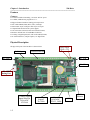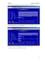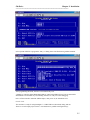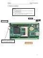
1
586-Drive™
C/C++ Programmable, 133 MHz 32-bit Web Controller
with Floating Point Unit, CompactFlash, 100M Ethernet,
High voltage I/Os, and 24-bit ADC / DACs
Technical Manual
1724 Picasso Avenue, Davis, CA 95618-0547, USA
Tel: 530-758-0180
Fax: 530-758-0181
Email: [email protected]
http://www.tern.com
COPYRIGHT
586-Drive, 586-Engine, 586-Engine-P, NT-Kit, and ACTF are trademarks of TERN, Inc.
Am188ES and Am186ES, ElanSC520 are trademarks of Advanced Micro Devices, Inc.
Paradigm C/C++ is a trademark of Paradigm Systems.
Windows95/98/2000/NT/ME/XP are trademarks of Microsoft Corporation.
Version 1.1
January 24, 2007
No part of this document may be copied or reproduced in any form or by any means
without the prior written consent of TERN, Inc.
© 1993-2006
1724 Picasso Avenue, Davis, CA 95618, USA
Tel: 530-758-0180 Fax: 530-758-0181
Email: [email protected]
http://www.tern.com
Important Notice
TERN is developing complex, high technology integration systems. These systems are
integrated with software and hardware that are not 100% defect free. TERN products are
not designed, intended, authorized, or warranted to be suitable for use in life-support
applications, devices, or systems, or in other critical applications. TERN and the Buyer
agree that TERN will not be liable for incidental or consequential damages arising from
the use of TERN products. It is the Buyer's responsibility to protect life and property
against incidental failure. TERN reserves the right to make changes and improvements to
its products without providing notice.
586-Drive
Chapter 1: Introduction
---------------------------------------------------------------------------------------------------------------
Chapter 1: Introduction
INTRODUCTION
The 586-Drive™ (5D) is a C/C++ programmable controller based on the 32-bit 133 MHz AMD Elan SC520. It
combines this high performance 586 generation processor with an extensive set of industrial I/O features on a
single-board.
The SC520 integrates an Am586 CPU and a high performance ANSI/IEEE 754 compliant hardware floating
point unit (FPU). The SC520 has a total of seven timers including PIT timers and GP timers, plus a software timer.
A real-time clock (RTC) provides a time-of-day calendar and 114 bytes of battery backed RAM. 13 user
programmable multifunctional I/O lines are available. One synchronous serial interface (SSI) supports full-duplex,
high speed bi-directional communication.
By default, 256KW low power 55 ns SRAM is installed to allow longer battery backup lifetime; this requires
slower 2 wait state access to memory. Optionally, if battery backup is not required, a high speed 20 ns SRAM can
be installed to allow higher performance zero wait state operation.
In additional to the on-board surface mount Flash, a 32-pin DIP IC socket allows using traditional user
application plug-in ROM/Flash. A 50-pin CompactFlash interface supports low cost, removable, up to 2 GB mass
storage CompactFlash cards with Windows compatible FAT file system support. The 5D can be powered by a
single unregulated DC power from 8V to 30V range with the on-board high-efficiency 5V switching regulator.
NETWORKING/CONNECTIVITY
An Fast Ethernet Module can be installed to provide 100M BaseT network connectivity. The hardware LSI
TCP/IP stack implements TCP/IP, UDP, ICMP and ARP in hardware. With 16KB internal transmit and receiving
buffer, the Ethernet module releases internet connectivity and protocol processing from the host processor. The
system can easily handle TCP/IP traffic of up to 200 Kbyte/s. Samples for HTTP, Telnet, FTP applications are
available.
Up to 4 RS232 serial ports (2 from SC520, and 2 SCC2691) are available. Two ports can be factory-configured
as RS485.
INDUSTRIAL I/O
By default, 7 high voltage inputs(30V), and 14 high voltage sinking drivers(ULN2003A) are installed in DIP
sockets. Each driver is capable of sinking 350 mA at 50V per line. They can directly drive solenoids, relays, or
lights. Optionally, 12 DAC channels can be installed in their place.
Four high isolation voltage photo couplers (PS2701, NEC) can be installed to provide optically isolated inputs.
Also, 16 additional input channels are provided with a 24-bit ADC(LTC2448), connected via hardware configurable
buffer resistors and screw terminal blocks. Variable resistor dividers can be installed to allow variable(up to 30V)
input range(as default, 0-5V). They can be processed as analog or digital signals. With a peak sample rate of 5
KHz, this ADC works well directly with analog signals from strain gages, current shunts, RTDs, resistive sensors,
and also work well directly with thermocouples in the differential mode. A precision reference(LT1019/REF02)
with a internal temperature sensor providing local temperature for thermocouple applications.
In addition, a 4 ch. 16-bit parallel ADC (AD7655, 0-5V) supports ultra high-speed (1 MHz conversion rate)
analog signal acquisition. The AD7655 contains two low noise, high bandwidth track-and-hold amplifiers that
allow simultaneous sampling on two channels.
Eight 16-bit digital to analog converters (TLC2600) can be installed to provide analog voltage (0-5V) outputs.
With the 388 pin BGA package of the SC520, repair support is not available. The 5D works with TERN
expansion boards including the UR8, C24, P100, and P300.
Special Note: The core of the Am520 CPU operates at +2.5V and the I/O operation at +3.3V. Also, the input for the
I/O is +5V compatable. Stresses above these can cause permanent damage to the SC520 CPU. Operation above
these values is not recommended, and can effect device reliability.
1-1
Chapter 1: Introduction
586-Drive
-------------------------------------------------------------------------------------------------------------
Features
Features:
• 151x82 mm. DIN rail mounting, 110 mA at 24V DC power
• 133 MHz, AMD SC520, program in C/C++
• High performance hardware floating point coprocessor
• Non volatile SRAM, Flash, RTC, timers, interrupts
• 4 RS232/485 Async serial ports and 1 Sync serial port
• CompactFlash and FAT16 file system support
• 4 ch 16-bit ADC (AD7655) and 8 16-bit DAC(LT2600)
• Hardware TCP/IP stack for 100M Base-T Ethernet
• 16 analog or digital inputs(30V) with 24-bit ADC(LT2448)
• 20+ Solenoid Drivers, 4 Opto-couplers, 10+ digital I/Os.
Physical Description
The physical layout of the 586-Drive is shown below.
7 HV Inputs
14 Solenoid Drivers
Power Input:
GND +12V
H3: SER1
H5: SCB
H4: SCA
H2: SER0
Debug Port
16 Analog/Digital
Inputs based on
24-bit ADC
LTC2448
1-2
8 Analog
Outputs
TLC2600
4 Inputs
16-bit ADC
AD7655, 1MHz
4 OPTOs
100M
Ethernet
586-Drive
Chapter 1: Introduction
--------------------------------------------------------------------------------------------------------------Expansions of the 586-Drive:
A P300 expansion board can be driven by the 586-Drive.
A low power graphic 192x128 pixel LCD can be driven by the 586-Drive.
1-3
Chapter 1: Introduction
586-Drive
-------------------------------------------------------------------------------------------------------------
Power On or Reset
Step 2 jumper
set?
YES
Validation of
battery back up?
NO
STEP 1
ACTF menu sent out through ser0
at 19200 baud
NO
Set the CS:IP in
internal RAM to
8000:0000
YES
STEP 2
Go to application
code CS:IP in
CPU's internal
RAM
Figure 1.1 Flow chart for ACTF operation
The “ACTF boot loader” resides in the 256KW on-board Flash chip (29F400). At power-on or RESET, the “ACTF”
will check the STEP 2 jumper. If STEP 2 jumper is not installed, the ACTF menu will be sent out from serial port0
at 19200 baud. If STEP 2 jumper is installed, the 586Drive will check for a valid battery back-up. If present, it will
go to the jump address stored in the CPU’s 114 bytes of general purpose RAM. Without a valid battery back up, it
will write the address 0x80000 to the inernal RAM, and then go to that address.
There is a 32-pin ROM socket on the 5D. The user’s application program must reside in SRAM for debugging in
STEP1, reside in battery-backed SRAM for the standalone field test in STEP2, and finally be programmed into
Flash for a complete product. For production, the user must produce an ACTF-downloadable HEX file for the
application, based on the DV-P. The “STEP2” jumper (J2 pins 38-40) must be installed for every productionversion board.
Step 1 settings
In order to correctly download a program in STEP1 with Paradigm C++ Debugger, the 5D must meet these
requirements:
1) 5860_115.HEX must be pre-loaded into Flash starting address 0x80000.
2) The CPU’s 114 bytes of RAM must have the correct jump address pointing at 5860_115.HEX, which is the
address 0x80000.
4) The STEP2 jumper must be installed on J2 pins 38-40.
For further information on programming the 586-Drive, refer to the Software chapter.
1-4
586-Drive
Chapter 1: Introduction
---------------------------------------------------------------------------------------------------------------
1.2 586-Drive Programming Overview
Steps for 5D based product development:
Preparation for debugging (By default, this is done in the factory !):
• Connect board to PC via serial link at 19,200, N, 8, 1 with Hyper Terminal
• Power-on without STEP 2 Jumper installed (J2.38 = J2.40)
• ACTF Menu will be sent from SER0 to external HyperTerminal at 19,200 baud
• Type ‘D’, then <enter> to download. Send Text File \tern\586\rom\l_29f400.hex
• Type ‘G04000’, then <enter> to execute HEX file just sent; will prepare flash
• Send Text File \tern\586\rom\5860_115.hex
• Type ‘G80000’, then <enter> to execute debug kernel
• Set STEP 2 Jumper (J2.38 = J2.40)
• Power-on/reset, ready to connect to Paradigm C/C++ for debugging
STEP 1: Debugging
• Launch Paradigm C/C++. Open \tern\586\samples\5d\5d.ide.
• Run sample code
• Create application using sample code.
• Use Paradigm C/C++ to edit, compile, link, locate, and remote debug
STEP 2: Standalone field test
• Downloaded code from STEP 1 is located by default at 0x0800:0x0000 in the
battery-backed SRAM
• Set Jump Address to point to downloaded code. Remove STEP 2 Jumper and
cycle power. Setup Hyper Terminal and see ACTF menu sent from 5D.
• Type ‘G08000’, then <enter> to jump to and execute application in SRAM
• Set STEP 2 jumper. 5D will execute application at 0x08000 at power-up.
• Test application. Return to STEP 1 as needed
STEP 3: Production (DV-P Kit required)
• Use Paradigm C/C++ to generate ACTF downloadable application HEX file.
• In Paradigm C/C++, open Target Expert for application. Set “Target Connection” to
“No Target/ROM”. Build target. Paradigm C/C++ will generate HEX file.
• Remove STEP 2 Jumper and see ACTF menu at hyper terminal. Download
“l_29f400.hex”. Same process as above. Type ‘G04000” to prepare flash
• Send you application HEX file. Type ‘G80000’ to execute code and set jump address
to point to you application in flash.
• Set STEP2 Jumper
1-5
586-Drive
Chapter 2: Installation
-----------------------------------------------------------------------------------------
Chapter 2: Installation
2.1 Software Installation
Refer to the Technical manual “Software_Kit.pdf” on TERN CD under tern_docs\manuals.
By manufacture default upon shipment, the 586-Drive should be ready to communicate with Paradigm C++
for debugging, with STEP2 jumper installed, CMOS RAM setup for 0x80000, and 5860_115 debug kernel
residing in Flash starting 0x80000. Power on, the on-board LED should blink twice indicating running
debug kernel. You DO NOT have to download debug kernel into flash again. You can SKIP the
operation discussed in 2.2 below.
2.2 Prepare 586-Drive for Paradigm C++ TERN Edition
This section uses RTLOAD to communicate with the ACTF utility while chapter refers to a hyper terminal.
Either works fine.
1) Start Paradigm C++. Select from Top menu: Tool, RTLOAD,
A HEX file Loader window will be shown.
2-1
586-Drive
Chapter 2: Installation
-----------------------------------------------------------------------------------------
2) F5=Select Baud, to setup 19200.
3) F8=Select .HEX file from c:\tern\586\rom\L_29F400.HEX
3) Power on the 586-Drive with the STEP2 jumper off, the ACTF menu will show up.
2-2
586-Drive
Chapter 2: Installation
-----------------------------------------------------------------------------------------
4) Caps Lock on your PC keyboard, Type “D” command, then enter.
5) F6 = Upload .HEX file, from PC to 586 SRAM.
2-3
586-Drive
Chapter 2: Installation
-----------------------------------------------------------------------------------------
6) Type “G04000” to run the “L_29F400” in SRAM. The first time you type “G04000” you will get an
error. Doing the “G04000” again, you will see as below
The 29F400 Flash sector 0x80000 to 0xFBFFF will be erased. It will then be ready to program Flash with
new DEBUG kernel file (c:\tern\586\rom\5860_115.hex), or user application .HEX.
7) F8= Select .HEX file, from c:\tern\586\rom\5860_115.hex.
2-4
586-Drive
Chapter 2: Installation
-----------------------------------------------------------------------------------------
8) F6=Upload .HEX file to program the 5860_115 debug kernel into Flash starting address 0x80000.
After programming the Flash, 586-Drive will automatically reset.
“G80000” to setup the CMOS RAM Jump Address, and start the DEBUG kernel. The on-board LED
should blink twice and then stay on; indicating 586-Drive is ready for remote debugging.
Power off the controller. Install the STEP2 Jumper, then power on, the LED blink twice.
Use F9 = Exit.
The 586-Drive is ready for using Paradigm C++ TERN Edition to download, debug, and run.
There are several sample projects in the c:\tern\586 directory (default working directory):
2-5
586-Drive
Chapter 2: Installation
----------------------------------------------------------------------------------------tern\586\led.ide: The most basic sample project, just flashes LED
tern\586\test.ide: Gives samples for serial ports, interrupts, timers. etc
tern\586\samples\5d\5d.ide: Shows how to use hardware components on board.
To open projects, go to “File” and open the sample project file, then build and download.
There are many sample programs under c:\tern\586\samples.
After you debug your application code, you can setup the 586-Drive to run in Standalone Mode.
Standalone Mode(STEP2):
By default, the Paradigm C++ TERN Edition will download your application code starting at 0x08000 in
the battery backed SRAM.
Power off 586-Drive. Remove STEP2 jumper. On PC side, click TOOL, RTLOAD.
Power on 586-Drive again without STEP2 jumper, then the ACTF menu should show up.
At the ACTF menu prompt, type “G08000” to setup the Jump Address and run your application.
Power off, install the STEP2 Jumper. Then at power on, controller will jump to 0x08000 in SRAM and run
your application.
2-6
586-Drive
Chapter 2: Installation
-----------------------------------------------------------------------------------------
2.3 Hardware Installation
Overview
• Connect debug serial cable:
For debugging (STEP 1), place IDE connector on SER0 (H2) with
red edge of cable at pin 1
• Connect wall transformer:
Connect 9V wall transformer to power and plug into power jack
adapter which installs in 2-pin screw terminal
Power Jack
STEP2 red jumper
Debug serial cable installed on SER0 (H2)
with red edge of cable aligned with pin 1.
Other end to PC’s COMx port.
Watchdog Jumper
2-7
586-Drive™
Chapter 3: Hardware
Chapter 3: Hardware
3.1 SC520 - Introduction
The 586-Drive is based on AMD Elan SC520 Microcontroller. It includes an industry-standard Am5x86
CPU with floating point unit (FPU). It provides a General-Purpose (GP) bus with programmable timing for
8 and 16-bit devices. A ROM/Flash controller supports on-board high performance code execution. An
enhanced programmable interrupt controller (PIC) prioritizes 22 interrupt levels with up to 15 external
sources. Two asynchronous UARTs can operate up to 1.15 M bit/s. A Synchronous Serial Interface (SSI)
offers full-duplex or half-duplex operation to support on-board ADC/DACs and user expansion. A real
time clock, a software timer, 3 GP timers, and 3 programmable interval timers are all included. Thirty-two
programmable I/O pins are on-board.
Please refer to the SC520 User’s Manual, SC520 Data Sheet, and SC520 Register Set Manual included on
TERN’s CD: amd_docs\sc520.
3.2 SC520 – Features
3.2.1 Clock
One 32.768 KHz and one 33.333 MHz crystal are installed to provide all the clocks required for CPU, Real
time clock, UART, timers, and clock output.
The CLKTEST (CLKT) signal is routed to J1 pin 4. Software can select to output one of 6 internal clocks,
including 32.768K, 1.8443 MHz, 18.432 MHz, 1.1882 MHz, 1.47456 MHz, and 36.864 MHz.
3.2.2 GP Bus Chip Selects
To Program GP bus Memory or I/O Chip Selects:
1) Config one of the 16 PAR regs(PAR11=Flash).
2) Config GP bus timing
3) Enable Chip select function on the desired pin in the CSPFS reg.
A total of 8 GP-bus Chip selects is supoorted on the 586Drive:
/GPCS0=P27=J2.37(PAR13), I/O 0x1800, Free to use for expansion.
/GPCS1=/ROMCS1=U16.22, 32-pin DIP socket, memory mapping 0x40000.
/GPCS2=/ROMCS2=SRAM (PAR14), Used by 586E/P/D, 0x0000-0x7ffff, memory mapping
/GPCS3=PITG2=U2.5(PAR15), I/O=0x2000, used by 5D ADC1655, SC1, SC2, L1, L2, and CF select
/GPCS4=TMRIN1=J2.1(PAR4), I/O=0x2800, free to use for expansion
/GPCS5=TMRIN0=J1.19(PAR5), I/O=0x3000, Free to use for expansion.
/GPCS6=TMROUT1=J2.5(PAR6), I/O=0x3800, Free to use.
/GPCS7=TMROUT0=J2.8=JP1.5(PAR7), Ehernet(i2chip) select, MEM mapping 0xf0000
3-1
Chapter 3: Hardware
586-Drive™
3.2.3 Programmable interrupt controller and external Interrupts
The Programmable Interrupt Controller (PIC) prioritizes 22 interrupt levels (P1-P22) with up to 15 external
sources (GPIRQ0-10 and INTA-D).
A programmable router must be programmed to map internal or external interrupt sources to the master or
two of slave interrupt controllers to provide different priorities, from P1 to P22.
All 15 external interrupt requests are programmed as edge sensitive, after 586_init();
An example map for P1 to P22 is listed below and demonstrated in the sample program 586_intx.c and is
included in the pre-built sample project \tern\586\test.ide.
//
There are 22 interrupt priority levels plus NMI
//
There are 15 external interrupt requests (GPIRQ0-10, /INTA-D)
//
Example internal interrupt map by TERN:
//
P1=Master PIC IR0, interrupt vector=0x40, PIT timer0
//
P2=Master PIC IR1, interrupt vector=0x41, GPIRQ0=PIO23=J2.33
//
P3=slave1 PIC IR0, interrupt vector=0x48, RTC
//
P4=slave1 PIC IR1, interrupt vector=0x49, GPIRQ1=PIO22=J2.23
//
P5=slave1 PIC IR2, interrupt vector=0x4a, GPIRQ2=PIO21=J2.21
//
P6=slave1 PIC IR3, interrupt vector=0x4b, GPIRQ3=PIO20=J2.19
//
P7=slave1 PIC IR4, interrupt vector=0x4c, GPIRQ4=PIO19=J2.20
//
P8=slave1 PIC IR5, interrupt vector=0x4d, FPU
//
P9=slave1 PIC IR6, interrupt vector=0x4e, /INTD=SCC=J3.14
//
P10=slave1 PIC IR7, interrupt vector=0x4f, GP timer1/INTC=J3.13
//
P11=Master PIC IR3, interrupt vector=0x43, SER2/0
//
P12=Master PIC IR4, interrupt vector=0x44, SER1
//
P13=Slave2 PIC IR0, interrupt vector=0x50, GP timer0
//
P14=Slave2 PIC IR1, interrupt vector=0x51, GPIRQ5=PIO18=J2.17
//
P15=Slave2 PIC IR2, interrupt vector=0x52, GPIRQ6=PIO17=J2.18
//
P16=Slave2 PIC IR3, interrupt vector=0x53, GPIRQ7=PIO16=J2.15
//
P17=Slave2 PIC IR4, interrupt vector=0x54, PIT timer1
//
P18=Slave2 PIC IR5, interrupt vector=0x55, GPIRQ8=PIO15=J2.16
//
P19=Slave2 PIC IR6, interrupt vector=0x56, GPIRQ9=PIO14=J2.6
//
P20=Slave2 PIC IR7, interrupt vector=0x57, GPIRQ10=PIO13=J2.8
//
P21=Master PIC IR6, interrupt vector=0x46, PIT Timer2/INTB=J3.12
//
P22=Master PIC IR7, interrupt vector=0x47, GP timer2/INTA=J3.11
See the sample program in c:\tern\586\samples\5e\586_intx.c for more details.
The 586-Drive uses vector interrupt functions to respond to external interrupts. Refer to the SC520 User’s
manual for more information about interrupt vectors.
3.2.4 Asynchronous Serial Ports
The SC520 has two 16450/16550-compatible asynchronous serial channels: SER0/2 and SER1. Both
asynchronous serial ports support the following:
•
•
•
•
•
•
•
•
3-2
Full-duplex operation,
5-, 6-, 7-, and 8-bit data transfers
Odd, even, and no parity
1, 1.5, or 2 stop bits
Error detection
Hardware flow control
Transmit and receive interrupts for each port
Maximum baud rate, up to 1.152 MHz
586-Drive™
Chapter 3: Hardware
The software drivers for each serial port implement a ring-buffered interrupt transmitting and receiving
arrangement. See the samples files s1_echo.c and s0_echo.c; s1_echo.c is included in the pre-built
sample project \tern\586\test.ide.
3.2.5 GP Timers
Three 16-bit General-Purpose Timers are on-board. Two external inputs, TIN0=J1.19(Expansion) and
TIN1=J2.1, can be used for the GP Timer0 and Timer1 to capture and count external pulses up to 33.333/4
MHz.
Timer 0 and Timer1 can output pulses on TOUT0=J2.8(i2chip) and TOUT1=J2.5.
GP Timers support interrupt on terminal count, continuous mode, and square wave generation.
Timer2 is not connected to any external pin. It can be used as an internal timer for real-time coding or
time-delay applications. It can also prescale timer0 and timer1.
The TIN0, TIN1m TOUT0, and TOUT1 pins are also shared with GP bus chip select lines.
See the sample programs timer02.c and tmr_out.c in the tern\586\samples\5e directory. GP timer
code is intergrated into several of the samples in the sample project \tern\586\test.ide.
3.2.6 PIT Timers
Three 16-bit Programmable Interval Timers (PIT) are on-board. Each PIT channel has one interrupt output.
Only PIT2 has an external output pin and can provide square wave output. All PITs supports interrupt on
terminal count, hardware-retriggerable one-shot and timer functions. See samples at c:\tern\586\samples\5e
directory for 586_pit0.c and pit2_out.c.
3.2.7 Software timers
The “software timer” is actually a hardware timer, which is intended to provide a millisecond timebase
with microsecond resolution. Ideal applications for this function include providing a system wide timebase,
or a precise measurement of the time between events. The software timer has a 16-bit microsecond counter
that increments with a period of one millisecond. This yields a maximum duration of 65.5 seconds. A
microsecond latch register that provides the number of microseconds since the last time that the
millisecond register was read.
The software timer provides a very efficient hardware timerbase for use by software. It is designed to
replace the traditional method of system timebase generation.
Traditional system timebase generation is accomplished by programming a timer to generate a periodic
interrupt. The interrupt service routine then increments a counter. This value is often kept in a global
variable, which can then be accessed by other code that needs to track time. The problem with this
traditional timebase is caused by interrupt latency and possible missed interrupt.
The software timer included can be used to resolve these problems.
See more details on AMD SC520 Users’ Manual, on TERN CD\amd_docs\sc520\sc520_user_manul.pdf
chapter 18.
3.2.8 SSI
A synchronous serial interface (SSI) provides full-duplex and half-duplex, bi-directional communication at
a software programmable SSI clock speed, from 64K Hz to 8MHz.586-Drive uses the SSI to interface to
the LTC2448 ADC and TLC2600 DAC. The user can use the SSI to interface many types of external serial
peripheral devices.
See the sample c:\tern\586\samples\5e\ssio.c.
3-3
Chapter 3: Hardware
586-Drive™
3.2.9 RTC
A battery backed up real-time clock (RTC) is included. The RTC consists of time-of-day clock with alarm
and a 100-year calendar. It has also a programmable periodic interrupt and 114 bytes of static user
RAM.When the 5D is powered off, the RTC (and 114 bytes of static RAM) is backed-up by the 3V battery
installed on the 586-Drive.
See samples 586_rtc.c and rtc_pint.c for more details.
3.2.10 Watchdog timer
The Watchdog timer included in SC520 is not disabled. The 586-Drive uses a 691 supervisor chip to
monitor the 5V power and provides an external watchdog. User can activate the 691 watchdog with a
jumper setting on H1. The watchdog timer provided a means to monitor proper software execution. If
software becomes stuck in an infinite loop, for example, the watchdog timer can reset the board to recover
to proper execution. If the watchdog timer is enabled (via install a jumper at H1), it must be reset via
software every 1.6 seconds, or sooner. If the watchdog timer is not reset after 1.6 seconds, the 691
supervisor will assert /RST, and reset the 586Drive. To reset the watchdog timer, user code needs to toggle
the PIO pin P4. With the watchdog jumper enabled, this routine should be arragned such that it is called
every 1.6 seconds are sooner.
3.2.11 Analog/digital inputs based on 24-bit ADC(LTC2448) with resister dividers
A 24-bit LTC2448 sigma-delta ADC can be installed. The ADC is driven by SC520 via the high
speed Sync Serial Port. The LTC2448 chip offers 8 ch. differential or 16 ch. single-ended input channels.
Variable speed/resolution settings can be configured. A peak single-channel output rate of 5 KHz can be
achieved.
The LTC2448 switches the analog input to a 2 pf capacitor at 1.8MHz with an equivalent input
resistance of 110K ohm. The ADC works well directly with strain gages, current shunts, RTDs, resistive
sensors, and 4-20mA current loop sensors. The ADC can also work well directly with thermocouples in
the differential mode. Installing a precision reference with a internal temperature sensor(LT1019, 2.5V)
provides local temperature measurement for thermocouple applications.
Protected resistor networkd are provided on-board to buffer the 16 channel inputs. In order to
support both analog or digital inputs with variable, higher voltage level, user configurable protection
resistor networks are designed into the board.
3-4
586-Drive™
Chapter 3: Hardware
The valid input voltage at the ADC(LTC2448) is 0-1.25V with an on-board 2.5V precision reference.
As default, 16 resistor dividers RP1-7 (20K+10K) are installed to provide valid analog input reading of 03.75V. Input voltage higher than 2.5V will be read by software as full scale.
The software source sample code on TERN CD, c:\tern\586\samples\5d\5d_ad24.c, allows user to modify
the input reading resolution. For digital inputs, only one byte reading is needed.
Protective Resistor
T1.17= IN16
20 K
RP4
20 K
B15, ADC
Analog input 0-3.75V
RP3
10 K
RP2
B01, ADC(LTC2448)
T1.2=IN2
Analog input 0-3.75V
RP1
10 K
GND, H6/H7
SUM, H6/H7
+REF, H6/H7
Landing Resistor
3.2.12 SC520 PIOs
The SC520 supports 32 user-programmable I/O lines (PIO). Each of these pins can be used as a userprogrammable input or output signal, if the interface function is not needed.
The 586-Drive PIO pins are 3.3V output and all inputs are 5V tolerant. Absolutely no voltage greater than
5V should be applied to any pins. Over 5V voltage input can cause permanent damage.
After power-on/reset, PIO pins default to various configurations. The initialization routine, sc_init();,
provided by TERN libraries reconfigures some of these pins as needed as:
P27=/GPCS0=J2.37 for 16-bit I/O operation.
P31=J2.38 as input for STEP2 jumper reading
P0 as output for on-board LED control
P1=/GPBHE as /BHE for 16-bit SRAM data bus high byte enable signal
P2 is used for on-board EEPROM(U0, SDA) and AD7655(U6, A0).
P3 is used by 24-bit ADC(LTC2448, Busy)
P4 is used as EEPROM SCL.
P5-P11 is for HV U19.8-2
P12=J2.12=J0.7(i2x DAT)
P13=J2.13=J0.1(i2x CLK)
P14=J2.14
Some PIO pins on the J2 header are free to use. PIO lines can be configured to operate as an
output or an input with a weak internal pull-up or pull-down resistor. A PIO pin’s behavior, either pull-up
or pull-down, is pre-determined and shown in the table below.
These configurations, as well as the processor-internal peripheral usage configurations, are listed below in
Table 3.1.
3-5
Chapter 3: Hardware
586-Drive™
PIO
Function
Power-On/Reset status
586-Drive Pin No.
586-Drive Initial
P0
P1
P2
GPALE
/GPBHE
GPRDY
Input with pull-up
Input with pull-up
Input with pull-up
Output for LED control
High byte enable /BHE
Input with pull-up
P3
GPAEN
Input with pull-up
P4
P5
P6
P7
P8
P9
P10
P11
P12
P13
P14
P15
P16
P17
P18
P19
P20
P21
P22
P23
GPTC
GPDRQ3
GPDRQ2
GPDRQ1
GPDRQ0
/GPDACK3
/GPDACK2
/GPDACK1
/GPDACK0
GPIRQ10
GPIRQ9
GPIRQ8
GPIRQ7
GPIRQ6
GPIRQ5
GPIRQ4
GPIRQ3
GPIRQ2
GPIRQ1
GPIRQ0
Input with pull-up
Input with pull-down
Input with pull-down
Input with pull-down
Input with pull-down
Input with pull-up
Input with pull-up
Input with pull-up
Input with pull-up
Input with pull-up
Input with pull-up
Input with pull-up
Input with pull-up
Input with pull-up
Input with pull-up
Input with pull-up
Input with pull-up
Input with pull-up
Input with pull-up
Input with pull-up
P24
P25
P26
P27
P28
P29
P30
P31
/GPBUFOE
/GPIOCS16
/GPMCS16
/GPCS0
/CTS2
/DSR2
/DCD2
/RIN2
Input with pull-up
Input with pull-up
Input with pull-up
Input with pull-up
Input with pull-up
Input with pull-up
Input with pull-up
Input with pull-up
LED L1 pin 2
SRAM U9.40
EE(U0.5,
SDA)
ADC7655(U5.3,
A0)
LTC2448
(U22.2, Busy)
EE(U0.6, SCL)
HV(U19.8)
HV(U19.7)
HV(U19.6)
HV(U19.5)
HV(U19.4)
HV(U19.3)
HV(U19.2)
J2.12,J0.7(i2x DAT)
J2.13,J0.1(i2x CLK)
J2 pin 14
J2 pin 16
J2 pin 15
J2 pin 18
J2 pin 17
OPTO 2
OPTO 4
OPTO 3
OPTO 1
J2 pin 33,
I2chip /INT=JP1.2
J2 pin 24
J2 pin 25
J2 pin 29
J2 pin 37
J2 pin 36
J2 pin 35
J2 pin 30
J2 pin 38
Input with pull-up
Input with pull-up
Input with pull-down
Input with pull-down
Input with pull-down
Input with pull-down
Input with pull-up
Input with pull-up
Input with pull-up
Input with pull-up
Input with pull-up
Input with pull-up
Input with pull-up
Input with pull-up
Input with pull-up
Input with pull-up
Input with pull-up
Input with pull-up
Input with pull-up
Input with pull-up
Input with pull-up
Input with pull-up
Input with pull-up
Input with pull-up*
16-bit I/O operation
Input with pull-up
Input with pull-up
Input with pull-up
STEP2 Jumper
Table 3.1 I/O pin default configuration after power-on or reset
C function in the library 586.lib can be used to initialize and to operate PIO pins.
void pio_init(char bit, char mode);
Where bit = 0-31 and mode = 0 (for interface function), 1 (for input), or 2 (for output).
Example:
pio_init(0, 2); will set P0 as output
pio_init(1, 0); will set P1 as /GPBHE
void pio_wr(char bit, char dat);
3-6
586-Drive™
Chapter 3: Hardware
pio_wr(0,1); set P0 pin high and the LED is off, if P0 is in output mode
pio_wr(0,0); set P0 pin low and the LED is on, if P0 is in output mode
unsigned int pio_rd(char port);
pio_rd (0); return 16-bit status of P0-P15, if corresponding pin is in input mode,
pio_rd (1); returns 16-bit status of P16-P31, if corresponding pin is in input mode,
Some of the I/O lines are used or shared by the 586-Drive system for on-board components.
Do not use these lines unless you are sure that you are not interfering with the
operation of such components
3.2.13 I/O Space
External I/O devices can use I/O mapping for access. You can access such I/O devices with inportb(port)
or outportb(port,dat). These functions will transfer one byte or word of data to the specified I/O address.
The external I/O space is 64K, ranging from 0x0000 to 0xffff.
The default GP bus timing is setup in sc_init(); as:
pokeb(MMCR,
_GPCSRT_, 0x01); // set the GP CS recovery time
pokeb(MMCR,
_GPCSPW_, 0x1f); // set the GP CS width
pokeb(MMCR,
_GPCSOFF_, 0x01); // set the GP CS offset
pokeb(MMCR,
_GPRDW_, 0x1f); // set the GP RD pulse width
pokeb(MMCR,
_GPRDOFF_, 0x0); // set the GP RD offset
pokeb(MMCR,
_GPWRW_, 0x1f); // set the GP WR pulse width
pokeb(MMCR,
_GPWROFF_, 0x0); // set the GP WR offset
User may modify the GP bus timing after sc_init();. Details regarding this can be found in the SC520
User’s Manual and SC520 Register Set Manual. Slower components, such as most LCD interfaces, might
find the maximum programmable wait state of 15 cycles still insufficient.
The table below shows the I/O mapping for each peripheral.
I/O space
Select
Location
Usage
0x2000-0x2004
0x2020
0x2040
0x2060-0x2074
0x2080-0x2094
0x20a0
0x20c0
0x20E0
/AD
/CV
HIT
/SC1
/SC2
/L1
/L2
/CF
U2.15 & U6.32
U6.35
H1.1
U17.14
U18.14
U24.11
U25.11
U5.32
AD7655 chip select
Begin conversion on ADC
Reset watchdog timer
SCC2691 Enable
SCC2691 Enable
74HC273 Chip select
74HC273 Chip select
CompactFlash chip select
3.2.14 Eight channel 16-bit DAC (LTC2600)
The LTC2600 is an eight channel 16-bit digital-to-analog converter (DAC) in an SO-8 package. It is
complete with a rail-to-rail voltage output amplifier capable of driving up to 15mA. It uses a 3-wire SPI
compatable serial interface and has an output range of 0-REF volts, making 1 LSB equal to REF/65535 V.
3-7
Chapter 3: Hardware
586-Drive™
The reference voltage input is routed to J4 pin 11 and by default is shorted to VCC via jumper at
J4.11=J4.9. The REF voltage must be greater than GND and less than VCC. The DAC outputs are routed
to the J4 pin header, pins 13-20.
The DAC is installed on the 586-Drive at location U8 and uses /RTS0 as the chip select. The synchronous
serial interface is used to send data to the device. Refer to the sample code, \tern\586\samples\5d\5d_da.c
for an example on driving the DAC.
The sample is also included in the pre-built sample project \tern\586\samples\5d\5d.ide.
Refer to the DAC data sheet for additional specifications; \tern_docs\parts\ltc2600.pdf.
3.2.15 Four channel, 16-bit ADC
The unique 16-bit parallel ADC (AD7655, 0-5V) supports ultra high-speed (1 MHz conversion rate)
analog signal acquisition. The AD7655 contains two low noise, high bandwidth track-and-hold amplifiers
that allow simultaneous sampling on two channels. Each track-and hold amplifier has a multiplexer in front
to provide a total of 4 channels analog inputs. The parallel ADC achieves very high throughput by
requiring only two CPU I/O operations (one start, one read) to complete a 16-bit ADC reading. With a
precision external 2.5V reference, the ADC accepts 0-5V analog inputs at 16-bit resolution of 0-65,535.
See sample program \tern\586\samples\5d\5d_ad.c for details on reading the ADC. The sample program is
also included in the pre-built sample project; \tern\586\samples\5d\5d.ide.
Refer to the data sheet for additional specifications; \tern_docs\parts\ad7655.pdf.
3.2.16 UART SCC2691
There are two UART SCC2691 chips (U17,U18), which are mapped into the 8-bit I/O address space at
0x2060-0x2074 and 0x2080-0x2094. The SCC2691 has a full-duplex asynchronous receiver/transmitter, a
quadruple buffered receiver data register, an interrupt control mechanism, programmable data format,
selectable baud rate for the receiver and transmitter, a multi-functional and programmable 16-bit
counter/timer, an on-chip crystal oscillator, and a multi-purpose input/output including RTS and CTS
mechanism.
The U17 chip uses signals /TXDA and /RXDA (routed to H4.2,H4.3 respectively), while the U18 chip uses
signals /TXDB and /RXDB (routed to H5.2,H5.3 respectively). The UART in location U17 is RS485
configurable, if the option is desired. By default, both UARTs use RS232 drivers.
See sample programs \tern\586\samples\5d\5d_sc1.c and \tern\586\samples\5d\5d_sc2.c for details on
activating both UARTs. The sample programs are also included in the pre-built sample project;
\tern\586\samples\5d\586d.ide.
3.2.17 EEPROM
A serial EEPROM of 512 bytes (24C04), or 2K bytes (24C16) can be installed in U0. The 586-Drive uses
the P4=SCL (serial clock) and P2=SDA (serial data) to interface with the EEPROM. The EEPROM can be
used to store important data such as a node address, calibration coefficients, and configuration codes. It
typically has 1,000,000 erase/write cycles. The data retention is more than 40 years. EEPROM can be read
and written by simply calling the functions ee_rd() and ee_wr().
3-8
586-Drive™
Chapter 3: Hardware
3.2.18 Protective high voltage inputs
In order to support high voltage digital signal input up to 30V, a Darlington Transistor Array (ULN2003A)
can be in U19. The maximum input voltage is 30V. The input pin has 12.7K resistance load to the GND.
You have to provide a pulled high signal input. A valid input low voltage is less than 0.8V, while a valid
input high voltage is higher than 3V and less than 30V.
5V
Darlington Transistor
K
Digital Input upto 30V DC
2.7 K
OUT
PIO pin
10 K
ULN2003A
GND
Figure 3.1 Darlington Transistors used as Protective High Voltage Inputs.
U19 may be set as input or output. By factory default, U19 is input. The input and output orientation for
the ULN2003A chip in the U19 socket are different.
Seven high voltage inputs cab be available on T2: O2-O8 while the ULN2003A is installed in U19 as input
mode:
ULN2003A is a 16-pin DIP, U19 is a 18-pin socket.
Install ULN2003A to register ULN2003A pin 1=U19.11
Force T2.1=O1 to GND first !!
T2.2=O2 to P11
T2.3=O3 to P10
T2.4=O4 to P9
T2.5=O5 to P8
T2.6=O6 to P7
T2.7=O7 to P6
T2.8=O8 to P5
Input up to 24 VDC voltage on screw terminal O2-O8, and read PIO line P11-P5.
While O2=24V, P11=low ; O2=0V, P11=high. In addition, the ULN2003A chip may be replaced with a
resistor pack to provide digital inputs or outputs to the terminal blocks.
Figure 3.2 Locations of user configurable Darlington Transistor Arrays.
3-9
Chapter 3: Hardware
586-Drive™
3.2.19 High-Voltage, High-Current Drivers
ULN2003A has high voltage, high current Darlington transistor arrays, consisting of seven silicon NPN
Darlington pairs on a common monolithic substrate. All channels feature open-collector outputs for sinking
350 mA at 50V, and integral protection diodes for driving inductive loads. Peak inrush currents of up to
600 mA sinking are allowed. By default, U21 and U20 are high-voltage driver outputs and U19 provides
high-voltage inputs.
J5.3 (VS)
=
J5.4 (GND)
U19
U21
U20
Figure 3.3 Default High Voltage Driver Configuration (U19 input; U20,U21 output).
These outputs may be paralleled to achieve high-load capability, although each driver has a maximum
continuous collector current rating of 350 mA at 50V. The maximum power dissipation allowed is 2.20 W
per chip at 25 degrees C (°C). The common substrate G is routed to T2 GND pins. All currents sinking in
must return to the T2 GND pin. A heavy gauge (20) wire must be used to connect the T2 GND terminal to
an external common ground return. K connects to the protection diodes in the ULN2003A chips and should
be tied to highest voltage in the external load system. K can be connected to an unregulated on board +12V
via J5 pin 1 and pin 2. ULN2003A is a sinking driver. An example of typical application wiring is shown
below.
O1
Solenoid
+12V
Power Supply
GND/SUB
J5.1 J5.2
ULN2003 TinyDrive
K
+12V
GND/SUB
Figure 3.4 Drive inductive load with high voltage/current drivers.
3-10
586-Drive™
Chapter 3: Hardware
Sourcing Option: U20 and U21 are also configurable as sourcing high-voltage inputs. See Figure 3.5 for
visual reference. This sourcing option MUST use UDN2982A sourcing chips, instead of the ULN2003A
sinking ones. Also, note the new jumper settings on J5.
J5.1 = J5.3
J5.2 = J5.4
U19
U21
U20
Figure 3.5 Optional High Voltage Driver Configuration (U20,U21 sourcing inputs).
3.2.20 Optional 192x128 pixel LCD
The 5D has a 20 pin Flex cable connector U31 to interface a 192x128 graphics LCD.
Since this interface is located underneath solenoid driver sockets U20 and U21, these two chips cannot be
installed with the LCD option. Also note that T2 screw terminal block cannot be installed as well to allow
for physical ease on the cable and POT.
For contrast adjustment, the LCD uses a POT (P7). See Figure 3.6.
For more information
c:\tern\586\samples\5d.
regarding
the
5D-LCD
interface,
see
sample
5d_lcd.c
in
project
LCD
interface
Contrast
POT
Figure 3.6 LCD interface & Contrast POT. Sockets U20, U21 cannot be installed.
3-11
Chapter 3: Hardware
586-Drive™
Figure 3.7 586D controller with LCD cable interface.
3.2.21 Opto-coupler Inputs
There are 4 opto-couplers available on the 5D.
Positive inputs OT1+ to OT4+ are routed to T1.25=OT1+, T1.24=OT2+, T1.22=OT3+, T1.21=OT4+.
Negative inputs are shared in pairs, however. Input OTA- (T1.26) corresponds to the OT1+ and OT2+
opto-couplers, while input OTB- (T1.23) corresponds to the OT3+ and OT4+ optos.
Inputs are protected by current limiting resistors installed at RP9. Inputs CPU-side are read through four
Port-1 PIO lines (P19-22), each corresponding to an opto-coupler.
See \tern\samples\586d\5d_opto.c for more details.
3.2.22 100 MHz BaseT Ethernet
An WizNet™ Fast Ethernet Module can be installed to provide 100M Base-T network connectivity. This
Ethernet module has a hardware LSI TCP/IP stack. It implements TCP/IP, UDP, ICMP and ARP in
hardware, supporting internet protocol DLC and MAC. It has 16KB internal transmit and receiving buffer
which is mapped into host processor’s direct memory. The host can access the buffer via high speed DMA
transfers. The hardware Ethernet module releases internet connectivity and protocol processing from the
host processor. It supports 4 independent stack connections simultaneously at a 4Mbps protocol processing
speed. An RJ45 8-pin connector is on-board for connecting to 10/100 Base-T Ethernet network. A software
library is available for Ethernet connectivity. Lines used by the Ethernet device include P23 and Timer 0
output TOUT0. These should not be user-activated if Ethernet option is installed.
3-12
586-Drive™
Chapter 3: Hardware
Figure 3.8 WizNet™ Ethernet Module
3.3 Power supplies and Supervisor with Watchdog Timer
Two supervisor chips monitor 5V and 3.3V and provide power failure detection, a watchdog and system
reset. The 2.5V power supply is used for the SC520 core and 3.3V supports SC520 I/O operation. Signal
lines on headers are 3.3V output, and 5V maximum input. Absolutely no voltage greater than 5V should be
applied to any pins. The 388 pin BGA package of SC520 makes repair support not available. All
components are soldered on board for highest reliability.
The 586-Drive™ can be powered with a single regulated 5V with the on-board 3.3V and 2.5V regulators.
The 586-Drive also includes an on-board switching regulator to provide 5V from an unregulated 8-30V
input.
A 691 (U7) supervisor chip is used to monitor the 5V power and a MIC8114 (U4) is designed to monitor
the 3.3V. The supervisor provides a watchdog timer, battery backup, power-on-reset delay, power-supply
monitoring, and power-failure warning. These will significantly improve system reliability.
Watchdog Timer
Setting a jumper on H1 activates the 691 watchdog timer. The watchdog timer provides a means of
verifying proper software execution. In the user's application program, calls to the function
inport(0x2040); that toggles the H1 pin1= HIT, should be arranged such that the HIT pin is accessed at
least once every 1.6 seconds. If the H1 jumper is installed and the HIT pin is not accessed within this timeout period, the watchdog timer pulls the WDO pin low, and asserts /RST. This automatic assertion of /RST
may recover the application program if something is wrong. When controllers are shipped from the factory
the H1 jumper is off, which disables the watchdog timer.
The SC520’s internal watchdog timer is disabled by default with sc_init().
Battery Backup Protection
The backup battery protection protects data stored in the SRAM and RTC. The battery-switch-over circuit
compares VCC to VBAT (+3 V lithium battery positive pin), and connects whichever is higher to the
VRAM (power for SRAM and RTC). Thus, the SRAM and the real-time clock RTC72423 are backed up.
In normal use, the lithium battery should last about 3-5 years without external power being supplied. When
the external power is on, the battery-switch-over circuit will select the VCC to connect to the VRAM.
3-13
Chapter 3: Hardware
586-Drive™
3.4 Headers and Connectors
3.4.1 Expansion Headers J1 and J2
There are two 20x2 0.1 spacing headers for 586-Drive expansion. Most signals are directly routed to the
SC520 processor. These signals are 3.3V and 5V tolerant, and any out-of-range voltages will damage the
board.
J2 Signal
GND
P31
P28
TXD0
RXD0
P30
TXD1
RXD1
P24
P17
P15
P14
P12
TOUT0
/INTA
GND
40
38
36
34
32
30
28
26
24
22
20
18
16
14
12
10
8
6
4
2
39
37
35
33
31
29
27
25
23
21
19
17
15
13
11
9
7
5
3
1
J1 Signal
VCC
P27
P29
P23
VCC
/INTB
P26
D15
/RST
RST
TIN0
D14
D13
P25
P18
P16
P13
SSI
SSO
SSC
TOUT1
/PITO2
TIN1
D12
/IOWR
/IORD
D11
D10
D9
D8
1
3
5
7
9
11
13
15
17
19
21
23
25
27
29
31
33
35
37
39
2
4
6
8
10
12
14
16
18
20
22
24
26
28
30
32
34
36
38
40
GND
CLKT
GND
D0
D1
D2
D3
D4
D5
D6
D7
GND
A7
A6
A5
A4
A3
A2
A1
A0
3.4.2 Header J4
The J4 (10x2 pins) headers on the 586-Drive provides the user with access to DAC outputs, ADC inputs.
See the schematic (5d-man.sch) attached in the last page of this manual for details.
J4 Signal
AA1
AA2
AB2
AB1
VCC
REF1
V2
V1
V7
V8
3-14
1
3
5
7
9
11
13
15
17
19
2
4
6
8
10
12
14
16
18
20
GND
GND
GND
GND
REF
V3
V4
V6
V5
586-Drive™
Chapter 3: Hardware
3.4.3 Headers T1 and T2
Both these headers are 26x1 screw terminals. T1 provides 16 ADC inputs and 4 opto-coupler inputs. T2
provides 7 HV inputs and 14 HV outputs. See schematic for more details. Default ULN2003A chips are
installed in U20 and U21 to provide 14 high voltage sinking drivers at O10-O16 and O18-O24. The O9
and O17 lines are not used for sinking drivers.
Optionally, two UDS2892 chips can be installed in U20 and U21 to provide 16 high voltage soucing
drivers. The O9 and O17 lines will be used here for sourcing.
HV INPUTS (O1 not used)
HV OUTPUTS
(O9 not used)
HV OUTPUTS
O1 O2 O3 O4 O5 O6 O7 O8
O9 O10 O11 O12 O13 O14 O15 O16
(O17 not used)
O17 O18 O19 O20 O21 O22 O23 O24
GND
T2
U19
U21
GND
U20
GND GND VCC
T1
IN1 IN2 IN3 IN4 IN5 IN6 IN7 IN8
ADC 24-bit Inputs (8 channels)
IN9 IN10 IN11 IN12 IN13 IN14 IN15 IN16
ADC 24-bit Inputs
(8 channels)
OT4+ OT3+ OTB- OT2+ OT1+ OTAOptocoupler Inputs(see section 3.2.21)
Figure 3.9 Default 586-Drive T1 & T2 Header Configuration.
3-15
+12VI
586-Drive
Chapter 4: Software
Chapter 4: Software
Please refer to the Technical Manual of the “C/C++ Development Kit for TERN 16-bit Embedded
Microcontrollers” for details on debugging and programming tools.
Guidelines, awareness, and problems in an interrupt driven environment
Although the C/C++ Development Kit provides a simple, low cost solution to application engineers, some
guidelines must be followed. If they are not followed, you may experience system crashes, PC hang-ups,
and other problems.
The debugging of interrupt handlers with the Remote Debugger can be a challenge. It is possible to debug
an interrupt handler, but there is a risk of experiencing problems. Most problems occur in multi-interruptdriven situations. Because the remote kernel running on the controller is interrupt-driven, it demands
interrupt services from the CPU. If an application program enables interrupt and occupies the interrupt
controller for longer than the remote debugger can accept, the debugger will time-out. As a result, your PC
may hang-up. In extreme cases, a power reset may be required to restart your PC.
For your reference, be aware that our system is remote kernel interrupt-driven for debugging.
The run-time environment on TERN controllers consists of an I/O address space and a memory address
space. I/O address space ranges from 0x0000 to 0xffff, or 64 KB. Memory address space ranges from
0x00000 to 0xfffff in real-mode, or 1 MB. These are accessed differently, and not all addresses can be
translated and handled correctly by hardware. I/O and memory mappings are done in software to define
how translations are implemented by the hardware. Implicit accesses to I/O and memory address space
occur throughout your program from TERN libraries as well as simple memory accesses to either code or
global and stack data. You can, however, explicitly access any address in I/O or memory space, and you
will probably need to do so in order to access processor registers and on-board peripheral components
(which often reside in I/O space) or non-mapped memory.
This is done with four different sets of similar functions, described below.
poke/pokeb
Arguments: unsigned int segment, unsigned int offset, unsigned int/unsigned char data
Return value: none
These standard C functions are used to place specified data at any memory space location. The segment
argument is left shifted by four and added to the offset argument to indicate the 20-bit address within
memory space. poke is used for writing 16 bits at a time, and pokeb is used for writing 8 bits.
The process of placing data into memory space means that the appropriate address and data are placed on
the address and data-bus, and any memory-space mappings in place for this particular range of memory
will be used to activate appropriate chip-select lines and the corresponding hardware component
responsible for handling this data.
peek/peekb
Arguments: unsigned int segment, unsigned int offset
Return value: unsigned int/unsigned char data
These functions retrieve the data for a specified address in memory space. Once again, the segment
address is shifted left by four bits and added to the offset to find the 20-bit address. This address is then
output over the address bus, and the hardware component mapped to that address should return either an
4-1
Chapter 4: Software
586Drive
8-bit or 16-bit value over the data bus. If there is no component mapped to that address, this function will
return random garbage values every time you try to peek into that address.
outport/outportb
Arguments: unsigned int address, unsigned int/unsigned char data
Return value: none
This function is used to place the data into the appropriate address in I/O space. It is used most often
when working with processor registers that are mapped into I/O space and must be accessed using either
one of these functions. This is also the function used in most cases when dealing with user-configured
peripheral components.
When dealing with processor registers, be sure to use the correct function. Use outport if you are dealing
with a 16-bit register.
inport/inportb
Arguments: unsigned int address
Return value: unsigned int/unsigned char data
This function can be used to retrieve data from components in I/O space. You will find that most hardware
options added to TERN controllers are mapped into I/O space, since memory space is valuable and is
reserved for uses related to the code and data. Using I/O mappings, the address is output over the address
bus, and the returned 16 or 8-bit value is the return value.
For a further discussion of I/O and memory mappings, please refer to the Hardware chapter of this
technical manual.
4.1 586.LIB
586.LIB is a C library for basic 586Drive operations. It includes the following modules: 586.OBJ,
SER0.OBJ, SER1.OBJ, SCC.OBJ. You need to link 586.LIB in your applications and include the
corresponding header files. The following is a list of the header files:
Include-file name
Description
586.H
SER0.H
SER1.H
SCC.H
timer/counter, ADC, DAC, RTC, Watchdog
Internal serial port 0/2
Internal serial port 1
External UART SCC2691
The 586.LIB was originally developed for the 586-Engine (the predecessor to the 586-Engine-D). Function
prototypes for the 586-Engine’s ADC and DAC were incorporated into 586.lib. The 586Drive does not
uses these same routines for its analog I/O. You must refer to the sample code in the 586\samples\5d
directory for examples on accessing the analog I/O on the 586Drive.
4-2
586-Drive
Chapter 4: Software
4.2 Functions in 586.OBJ
4.2.1 586Drive Initialization
sc_init
This function should be called at the beginning of every program running on 586Drive. It provides default
initialization and configuration of the various I/O pins, interrupt vectors, sets up I/O, and provides other
processor-specific updates needed at the beginning of every program.
There are certain default pin modes and interrupt settings you might wish to change. With that in mind, the
basic effects of sc_init are described below. For details regarding register use, you will want to refer to the
AMD SC520 Microcontroller User’s manual.
•
Initialize the programmable interrupt controller. Setup the master interrupt controller at vector
0x40. The slave1 interrupt vector at 0x48, and slave 2 interrupt vector at 0x50.
•
Initialize /ROMCS1 chip select to support the 8-bit I/O starting 0x1000, and the /GPCS0 to support
16-bit I/O starting address at 0x1800.
•
Disable SDRAM
•
Initialize default GP-bus chip select timing as
pokeb(MMCR, _GPCSRT_, 0x01); // set the GP CS recovery time
pokeb(MMCR, _GPCSPW_, 0x1f); // set the GP CS width
pokeb(MMCR, _GPCSOFF_, 0x01); // set the GP CS offset
pokeb(MMCR, _GPRDW_, 0x1f); // set the GP RD pulse width
pokeb(MMCR, _GPRDOFF_, 0x0); // set the GP RD offset
pokeb(MMCR, _GPWRW_, 0x1f); // set the GP WR pulse width
pokeb(MMCR, _GPWROFF_, 0x0); // set the GP WR offset
•
Initialize and configure PIO ports for default operation. All pins are set up as default input, except
for P31, P27, P2, and P0.
The GP chip selects are set to 0x1f wait states, by default. This makes it possible to interface with many
slower external peripheral components. If you require faster I/O access, you can modify this number down
as needed.
A CLKT signal is routed to J1 pin 4 for the external user clock. The CLKT can be selected as
void clkt_sel
Arguments: unsigned char clk
Return value: none.
The CLKT pin is programmed as an output (CLKTEST).
When programmed as output, CLKT output one of the 6 internal clocks:
void clkt_sel(unsigned char clk);
where:
clk=000, RTC (32.768 KHz)
clk=001, UART (1.8443 MHz)
clk=010, UART (18.432 MHz)
clk=011, PIT (1.1882 MHz)
clk=100, PLL1 (1.47456 MHz)
clk=101, PLL2 (36.864 MHz)
clk=110-111, CLKT=0
4-3
Chapter 4: Software
586Drive
4.2.2 External Interrupt Initialization
The programmable interrupt controller consistes of a system of three individual interrupt controllers
(Master, Slave1, and Slave2), each has eight interrupt channels. A total of 22 interrupt priority levels are
supported. A programmable interrupt router handles routing of various external and internal interrupt
sources to the 22 interuupt channels. TERN recommends an interrupt map as follows;
There are 22 interrupt priority levels plus NMI
There are 15 external interrupt requests (GPIRQ0-10, /INTA-D). You must
provide a low to high edge to generate an interrupt
Example internal interrupt map by TERN:
P1=Master PIC IR0, interrupt vector=0x40, PIT timer0
P2=Master PIC IR1, interrupt vector=0x41, GPIRQ0=PIO23=J2.33
P3=slave1 PIC IR0, interrupt vector=0x48, RTC
P4=slave1 PIC IR1, interrupt vector=0x49, GPIRQ1=PIO22=J2.23
P5=slave1 PIC IR2, interrupt vector=0x4a, GPIRQ2=PIO21=J2.21
P6=slave1 PIC IR3, interrupt vector=0x4b, GPIRQ3=PIO20=J2.19
P7=slave1 PIC IR4, interrupt vector=0x4c, GPIRQ4=PIO19=J2.20
P8=slave1 PIC IR5, interrupt vector=0x4d, FPU
P9=slave1 PIC IR6, interrupt vector=0x4e, /INTD=SCC=J3.14
P10=slave1 PIC IR7, interrupt vector=0x4f, GP timer1/INTC=J3.13
P11=Master PIC IR3, interrupt vector=0x43, SER2/0
P12=Master PIC IR4, interrupt vector=0x44, SER1
P13=Slave2 PIC IR0, interrupt vector=0x50, GP timer0
P14=Slave2 PIC IR1, interrupt vector=0x51, GPIRQ5=PIO18=J2.17
P15=Slave2 PIC IR2, interrupt vector=0x52, GPIRQ6=PIO17=J2.18
P16=Slave2 PIC IR3, interrupt vector=0x53, GPIRQ7=PIO16=J2.15
P17=Slave2 PIC IR4, interrupt vector=0x54, PIT timer1
P18=Slave2 PIC IR5, interrupt vector=0x55, GPIRQ8=PIO15=J2.16
P19=Slave2 PIC IR6, interrupt vector=0x56, GPIRQ9=PIO14=J2.6
P20=Slave2 PIC IR7, interrupt vector=0x57, GPIRQ10=PIO13=J2.8
P21=Master PIC IR6, interrupt vector=0x46, PIT Timer2/INTB=J3.12
P22=Master PIC IR7, interrupt vector=0x47, /INTA=J3.11
A spurious interrupt is defined as a "Not Valid" interrupt.
A Spurious Interrupt on any IR line generates the same vector number
as an IR7 request. The spurious interrupt, however, does not set the
in-service bit for IR7. Therefore, an IR7 isr must check the isr register to determine the interrupt source
was a
valid IR7 (the in-service bit is set),
or a spurious interrupt (the in-service bit is cleared)
Functions
void
void
void
void
void
void
void
void
void
void
void
4-4
nmi_init(void); // nmi interrupt handler initialization
int0_init(char i, void interrupt far (* int0_isr)())
int1_init(char i, void interrupt far (* int1_isr)())
int2_init(char i, void interrupt far (* int2_isr)())
int3_init(char i, void interrupt far (* int3_isr)())
int4_init(char i, void interrupt far (* int4_isr)())
int5_init(char i, void interrupt far (* int5_isr)())
int6_init(char i, void interrupt far (* int6_isr)())
int7_init(char i, void interrupt far (* int7_isr)())
int8_init(char i, void interrupt far (* int8_isr)())
int9_init(char i, void interrupt far (* int9_isr)())
586-Drive
void
Chapter 4: Software
intD_init(char i, void interrupt far (* intD_isr)())
For a detailed discussion involving the interrupt, the user should refer to Chapter 15 of the AMD SC520
Microcontroller User’s Manual.
TERN provides functions to enable/disable all of the external interrupts. The user can call any of the
interrupt init functions listed for this purpose. The first argument indicates whether the particular interrupt
should be enabled, and the second is a function pointer to an appropriate interrupt service routine that
should be used to handle the interrupt. The TERN libraries will set up the interrupt vectors correctly for
the specified external interrupt line.
At the end of interrupt handlers, the appropriate in-service bit for the IR signal currently being handled
must be cleared. This can be done using the Nonspecific EOI command. At initialization time, interrupt
priority was placed in Fully Nested mode. This means the current highest priority interrupt will be handled
first, and a higher priority interrupt will interrupt any current interrupt handlers. So, if the user chooses to
clear the in-service bit for the interrupt currently being handled, the interrupt service routine just needs to
issue the nonspecific EOI command to clear the current highest priority IR.
void intx_init
Arguments: unsigned char i, void interrupt far(* intx_isr) () )
Return value: none
These functions can be used to initialize any one of the external interrupt channels (for pin locations and
other physical hardware details, see the Hardware chapter). The first argument i indicates whether this
particular interrupt should be enabled or disabled. The second argument is a function pointer, which will
act as the interrupt service routine. The overhead on the interrupt service routine, when executed, is about
20 µs.
By default, the interrupts are all disabled after initialization. To disable them again, you can repeat the call
but pass in 0 as the first argument.
I/O Initialization
Two ports of 16 I/O pins each are available on the 586Drive. Hardware details regarding these PIO lines
can be found in the Hardware chapter.
Several functions are provided for access to the PIO lines. At the beginning of any application where you
choose to use the PIO pins as input/output, you will probably need to initialize these pins in one of the
three available modes. Before selecting pins for this purpose, make sure that the peripheral mode operation
of the pin is not needed for a different use within the same application.
You should also confirm the PIO usage that is described above within sc_init(). During initialization,
several lines are reserved for TERN usage and you should understand that these are not available for your
application. There are several PIO lines that are used for other on-board purposes. These are all described
in some detail in the Hardware chapter of this technical manual. For a detailed discussion on the I/O ports,
please refer to Chapter 23 of the AMD SC520 User’s Manual.
Please see the sample program 586_pio.c in tern\586\samples\5e. You will also find that these functions
are used throughout TERN sample files, as most applications do find it necessary to re-configure the PIO
lines.
The function pio_wr and pio_rd can be quite slow when accessing the PIO pins. Depending on the pin
being used, it might require from 5-10 us. The maximum efficiency you can get from the PIO pins occur if
you instead modify the PIO registers directly with an poke instruction Performance in this case will be
around 1-2 us to toggle any pin. For example: poke(MMCR, _PIOSET15_0_, m);
void pio_init
Arguments:
Return value:
char bit, char mode
none
4-5
Chapter 4: Software
586Drive
bit refers to any one of the 32 PIO lines, 0-31.
mode refers to one of 3 modes of operation.
• 0, Interface operation
• 1, input with pullup/down
• 2, output
unsigned int pio_rd:
Arguments:
char port
Return value: byte indicating PIO status
Each bit of the returned 16-bit value indicates the current I/O value for the PIO pins in the selected port.
void pio_wr:
Arguments:
Return value:
char bit, char dat
none
Writes the passed in dat value (either 1/0) to the selected PIO.
4.2.3 GPTimer Units
The three GP timers present on the 586Drive can be used for a variety of applications
These timers are controlled and configured through a mode register that is specified using the software
interfaces. The mode register is described in detail in chapter 17 of the AMD SC520 User’s Manual.
Two of the timers, Timer0 and Timer1 has external pulses output and counter inputs.
It is also possible to use the output of Timer2 to pre-scale one of the other timers, since 16-bit resolution at
the maximum clock rate specified gives you only 150 Hz. Only by using Timer2 can you slow this down
even further. The sample files timer02.c and timer12.c, located in tern\586\samples\5e, demonstrate this.
void t0_init
void t1_init
Arguments: int tm, int ta, int tb, void interrupt far(*t_isr)()
Return values: none
Both of these timers have two maximum counters (MAXCOUNTA/B) available. These can all be specified
using ta and tb. The argument tm is the value that you wish placed into the T0CON/T1CON mode
registers for configuring the two timers.
The interrupt service routine t_isr specified here is called whenever the full count is reached, with other
behavior possible depending on the value specified for the control register.
void t2_init
Arguments: int tm, int ta, void interrupt far(*t_isr)()
Return values: none.
Timer2 behaves like the other timers, except it only has one max counter available.
4.2.4 Other library functions
On-board supervisor MAX691 or LTC691
The watchdog timer offered by the MAX691 or LTC691 offers an excellent way to monitor improper
program execution. If the watchdog timer (H1) jumper is set, the function hitwd() must be called every
1.6 seconds of program execution. If this is not executed because of a run-time error, such as an infinite
loop or stalled interrupt service routine, a hardware reset will occur.
4-6
586-Drive
Chapter 4: Software
void hitwd
Arguments: none
Return value: none
Resets the supervisor timer for another 1.6 seconds.
void led
Arguments: int ledd
Return value: none
Turns the on-board LED on or off according to the value of ledd.
Real-Time Clock
A real-time clock is included in the SC520, and can be used to keep track of real time. Backed up by a
lithium-coin battery, the real time clock can be accessed and programmed using two interface functions.
There are two common data structure used to access and use both interfaces.
// SC520 RTC data structure
typedef struct{
unsigned char sec;
unsigned char alarm_sec;
unsigned char min;
unsigned char alarm_min;
unsigned char hour;
unsigned char alarm_hour;
unsigned char day_week;
unsigned char day_month;
unsigned char month;
unsigned char year;
} RTCTIME;
// Real time data structure
typedef struct{
unsigned char sec1; One second digit.
unsigned char sec10; Ten second digit.
unsigned char min1; One minute digit.
unsigned char min10; Ten minute digit.
unsigned char hour1; One hour digit.
unsigned char hour10; Ten hour digit.
unsigned char day1; One day digit.
unsigned char day10; Ten day digit.
unsigned char mon1; One month digit.
unsigned char mon10; Ten month digit.
unsigned char year1; One year digit.
unsigned char year10; Ten year digit.
unsigned char wk; Day of the week.
} TIM;
4-7
Chapter 4: Software
586Drive
int rtc_rd
Arguments: TIM *r
Return value: int error_code
This function places the current value of the real time clock within the argument r structure. The structure
should be allocated by the user. This function returns 0 on success and returns 1 in case of error, such as
the clock failing to respond.
int rtc_rds
Arguments: char* realTime
Return value: int error_code
This function places a string of the current value of the real time clock in the char* realTime.
The text string has a format of “year1000 year100 year10 year1 month10 month1 day10 day1 hour10
hour1 min10 min1 second10 second1”. For example” 19991220081020” represents year 1999, December
20th, Eight o’clock, 10 minutes, and 20 seconds.
This function returns 0 on success and returns 1 in case of error, such as the clock failing to respond.
Void rtc_init
Arguments: char* t, RTCTIME *rtcp
Return value: none
This function is used to initialize and set a value into the real-time clock. The argument t should be a nullterminated byte array that contains the new time value to be used.
The RTCTIME data structure will be initialized based on the string t.
The byte array should correspond to { weekday, year10, year1, month10, month1, day10, day1, hour10,
hour1, minute10, minute1, second10, second1, 0 }.
If, for example, the time to be initialized into the real time clock is June 5, 1998, Friday, 13:55:30, the byte
array would be initialized to:
unsigned char t[14] = { 5, 9, 8, 0, 6, 0, 5, 1, 3, 5, 5, 3, 0 };
Delay
In many applications it becomes useful to pause before executing any further code. There are functions
provided to make this process easy. For applications that require precision timing, you should use
hardware timers, (Software Timer of SC520) provided on-board for this purpose.
void delay0
Arguments: unsigned int t
Return value: none
This function is just a simple software loop. The actual time that it waits depends on processor speed as
well as interrupt latency. The code is functionally identical to:
While(t) { t--; }
Passing in a t value of 600 causes a delay of approximately 1 ms.
void delay_ms
Arguments: unsigned int
Return value: none
This function is similar to delay0, but the passed in argument is in units of milliseconds instead of loop
iterations. Again, this function is highly dependent upon the processor speed. NOT accurate at all.
4-8
586-Drive
Chapter 4: Software
void sc_rst
Arguments: none
Return value: none
This function is similar to a hardware reset, and can be used if your program needs to re-start the board for
any reason. Depending on the current hardware configuration, this might either start executing code from
the DEBUG ROM or from some other address.
4.3 Functions in SER0.OBJ/SER1.OBJ
The functions described in this section are prototyped in the header file ser0.h and ser1.h in the directory
tern\586\include.
The internal asynchronous serial ports are functionally identical. SER0/2 is used by the DEBUG ROM
provided as part of the TERN EV/DV-P software kits for communication with the PC. As a result, you
will not be able to debug code directly written for serial port 0, but you can run it in STEP2.
Two asynchronous serial ports are integrated in the SC520: SER0/2 and SER1. Both ports have baud rates
based on the system clock, and can operate at a maximum of 1.152 Mbaud.
By default, SER0 is used by the DEBUG ROM for application download/debugging in STEP 1. We will
use SER1 as the example in the following discussion; any of the interface functions that are specific to
SER1 can be easily changed into function calls for SER0. For details, you should see both chapter 21 of the
SC520 Microprocessor User’s Manual and the schematic of the 586Drive provided at the end of this
manual. TERN interface functions make it possible to use one of a number of predetermined baud rates.
These baud rates are achieved by specifying a divisor. The following table shows the function arguments
that express each baud rate, to be used in TERN functions. These are based on a 33.333 MHz external
crystal. Note: Only up to 115,200 BAUD has been tested in house. (10/25/00)
Function Argument
Baud Rate
1
300
2
600
3
2400
4
4800
5
7200
6
9600
7
14,400
8
19,200
9
38,400
10
57,600
11
115,200
12
114,000
13
192,000
4-9
Chapter 4: Software
586Drive
Function Argument
Baud Rate
14
288,000
15
576,000
16
1,152,000
Table 4.1 Baud rate values
After initialization by calling s1_init(), SER1 is configured as a full-duplex interrupt-driven serial port
and is ready to transmit/receive serial data at one of the specified 16 baud rates.
An input buffer, ser1_in_buf (whose size is specified by the user), will automatically store the
receiving serial data stream into the memory. The user only has to check the buffer status with
serhit1() and take out the data from the buffer with getser1(), if any. The input buffer is used as a
circular ring buffer, as shown in Figure 4.1
ibuf
in_tail
in_head
ibuf+isiz
Figure 4.1 Circular ring input buffer
The input buffer (ibuf), buffer size (isiz), and baud rate (baud) are specified by the user with s1_init()
with a default mode of 8-bit, 1 stop bit, no parity. After s1_init() you can set up a new mode with
different numbers for data-bit, stop bit, or parity by directly accessing the Serial Port 0/1 Control Register
if necessary, as described in chapter 21 of the SC520 manual for asynchronous serial ports.
Due to the nature of high-speed baud rates and possible effects from the external environment, serial input
data will automatically fill in the buffer circularly without stopping, regardless of overwrite. If the user
does not take out the data from the ring buffer with getser1() before the ring buffer is full, new data
will overwrite the old data without warning or control. Thus it is important to provide a sufficiently large
buffer if large amounts of data are transferred. For example, if you are receiving data at 9600 baud, a 4KB buffer will be able to store data for approximately four seconds.
However, it is always important to take out data early from the input buffer, before the ring buffer rolls
over. You may designate a higher baud rate for transmitting data out and a slower baud rate for receiving
data. This will give you more time to do other things, without overrunning the input buffer. You can use
serhit1() to check the status of the input buffer and return the offset of the in_head pointer from the
in_tail pointer. A return value of 0 indicates no data is available in the buffer.
You can use getser1() to get the serial input data byte by byte using FIFO from the buffer. The in_tail
pointer will automatically increment after every getser1() call. It is not necessary to suspend external
devices from sending in serial data with /RTS. Only a hardware reset or s1_close() can stop this
receiving operation.
For transmission, you can use putser1() to send out a byte, or use putsers1() to transmit a
character string. You can put data into the transmit ring buffer, s1_out_buf, at any time using this
method. The transmit ring buffer address (obuf) and buffer length (osiz) are also specified at the time of
initialization. The transmit interrupt service will check the availability of data in the transmit buffer. If
there is no more data (the head and tail pointers are equal), it will disable the transmit interrupt. Otherwise,
it will continue to take out the data from the out buffer, and transmit. After you call putser1() and
transmit functions, you are free to do other tasks with no additional software overhead on the transmitting
4-10
586-Drive
Chapter 4: Software
operation. It will automatically send out all the data you specify. After all data has been sent, it will clear
the busy flag and be ready for the next transmission.
The sample program ser1_0.c demonstrates how a protocol translator works. It would receive an input
HEX file from SER1 and translate every ‘:’ character to ‘?’. The translated HEX file is then transmitted
out of SER0. This sample program can be found in tern\586\samples\5e.
Software Interface
Before using the serial ports, they must be initialized.
There is a data structure containing important serial port state information that is passed as argument to the
TERN library interface functions. The COM structure should normally be manipulated only by TERN
libraries. It is provided to make debugging of the serial communication ports more practical. Since it
allows you to monitor the current value of the buffer and associated pointer values, you can watch the
transmission process.
The two serial ports have similar software interfaces. Any interface that makes reference to either s0 or
ser0 can be replaced with s1 or ser1, for example. Each serial port should use its own COM structure, as
defined in 586.h.
typedef struct {
unsigned char ready; /* TRUE when ready */
unsigned char baud;
unsigned char mode;
unsigned char iflag; /* interrupt status
*/
unsigned char *in_buf; /* Input buffer */
int in_tail;
/* Input buffer TAIL ptr */
int in_head;
/* Input buffer HEAD ptr */
int in_size;
/* Input buffer size */
int in_crcnt;
/* Input <CR> count */
unsigned char in_mt;
/* Input buffer FLAG */
unsigned char in_full;
/* input buffer full */
unsigned char *out_buf;
/* Output buffer */
int out_tail;
/* Output buffer TAIL ptr */
int out_head;
/* Output buffer HEAD ptr */
int out_size;
/* Output buffer size */
unsigned char out_full;
/* Output buffer FLAG */
unsigned char out_mt;
/* Output buffer MT */
unsigned char tmso;
// transmit macro service operation
unsigned char rts;
unsigned char dtr;
unsigned char en485;
unsigned char err;
unsigned char node;
unsigned char cr; /* scc CR register
*/
unsigned char slave;
unsigned int in_segm;
/* input buffer segment */
unsigned int in_offs;
/* input buffer offset */
unsigned int out_segm;
/* output buffer segment */
unsigned int out_offs;
/* output buffer offset */
unsigned char byte_delay;
/* V25 macro service byte delay */
} COM;
sn_init
Arguments: unsigned char b, unsigned char* ibuf, int isiz, unsigned char* obuf, int osiz, COM* c
Return value: none
4-11
Chapter 4: Software
586Drive
This function initializes either SER0 or SER1 with the specified parameters. b is the baud rate value
shown in Table 4.1. Arguments ibuf and isiz specify the input-data buffer, and obuf and osiz specify the
location and size of the transmit ring buffer.
The serial ports are initialized for 8-bit, 1 stop bit, no parity communication.
There are a couple different functions used for transmission of data. You can place data within the output
buffer manually, incrementing the head and tail buffer pointers appropriately. If you do not call one of the
following functions, however, the driver interrupt for the appropriate serial-port will be disabled, which
means that no values will be transmitted. This allows you to control when you wish the transmission of
data within the outbound buffer to begin. Once the interrupts are enabled, it is dangerous to manipulate the
values of the outbound buffer, as well as the values of the buffer pointer.
putsern
Arguments: unsigned char outch, COM *c
Return value: int return_value
This function places one byte outch into the transmit buffer for the appropriate serial port. The return value
returns one in case of success, and zero in any other case.
putsersn
Arguments: char* str, COM *c
Return value: int return_value
This function places a null-terminated character string into the transmit buffer. The return value returns one
in case of success, and zero in any other case.
serhitn() should be called before trying to retrieve data.
serhitn
Arguments: COM *c
Return value: int value
This function returns 1 as value if there is anything present in the in-bound buffer for this serial port.
getsern
Arguments: COM *c
Return value: unsigned char value
This function returns the current byte from sn_in_buf, and increments the in_tail pointer. Once again, this
function assumes that serhitn has been called, and that there is a character present in the buffer.
getsersn
Arguments: COM c, int len, char* str
Return value: int value
This function fills the character buffer str with at most len bytes from the input buffer. It also stops
retrieving data from the buffer if a carriage return (ASCII: 0x0d) is retrieved.
This function makes repeated calls to getser, and will block until len bytes are retrieved. The return value
indicates the number of bytes that were placed into the buffer.
4-12
586-Drive
Chapter 4: Software
Be careful when you are using this function. The returned character string is actually a byte array
terminated by a null character. This means that there might actually be multiple null characters in the byte
array, and the returned value is the only definite indicator of the number of bytes read. Normally, we
suggest that the getsers and putsers functions only be used with ASCII character strings. If you are
working with byte arrays, the single-byte versions of these functions are probably more appropriate.
Miscellaneous Serial Communication Functions
One thing to be aware of in both transmission and receiving of data through the serial port is that TERN
drivers only use the basic serial-port communication lines for transmitting and receiving data. Hardware
flow control in the form of CTS (Clear-To-Send) and RTS (Ready-To-Send) is not implemented. There
are, however, functions available that allow you to check and set the value of these I/O pins appropriate for
whatever form of flow control you wish to implement. Before using these functions, you should once
again be aware that the peripheral pin function you are using might not be selected as needed. For details,
please refer to the SC520 User’s Manual.
char sn_cts(void)
Retrieves value of CTS pin.
void sn_rts(char b)
Sets the value of RTS to b.
Completing Serial Communications
After completing your serial communications, you can re-initialize the serial port with s1_init(); to reset
default system resources.
sn_close
Arguments: COM *c
Return value: none
This closes down the serial port, by shutting down the hardware as well as disabling the interrupt.
The asynchronous serial I/O ports available on the SC520 have many other features that might be useful
for your application. If you are truly interested in having more control, please read Chapter 21 of the
manual for a detailed discussion of other features available to you.
4.4 Functions / Routines not in 586.lib
4.4.1 4 channel 16-bit ADC, AD7655
The ADC is accessed using a few different control lines. The control lines are summarized below:
Control Line
Description / Function
/CV
Begin conversion. I/O address 0x2020
/AD
Read conversion. 0x2000 for AB1, AB2 and 0x2004 for AA1 and AA2
P2
MUX select. P2 high selects AA2, AB2. P2 low selects AA1, AB1
A2
A2 = /AD&0x0004.
4-13
Chapter 4: Software
586Drive
The following process must be followed to read the ADC:
pio_wr ( 2 , hi_lo) ;
inport ( CV ) ;
wait for 2.5 µs
inport ( ADA ) ;
inport ( ADB ) ;
Where
hi_lo
ADA
0
A2 = 1
0
1
ADB
AA1
A2 = 0
A2 = 1
1
Read channel
AB1
AA2
A2 = 0
AB2
Refer to the sample program \tern\586\samples\5d\5d_ad.c and data sheet \tern_docs\parts\ad7655.pdf for
additional details. Also refer to the pre-built sample project \tern\586\samples\5d\586d.ide.
4.4.2 8 channel 16-bit DAC
To access the DAC use the routine called ‘da_2600’ found in the \tern\586\samples\5d\5d_da.c sample
program. You must copy the routine from the source file into your application, as it is not part of a library.
The function ‘da_2600’ takes two arguments. The first is the channel to write to, with the valid range 0-7.
The second is the output value, ranging from 0 – 65535. See the sample program for additional details.
4.4.3 16 channel 24-bit ADC
Delta-Sigma ADC LTC2448
The LTC2448 ADC (U22) provides 16 channels of 0-2.5V analog single-ended (24 differential) inputs (or
0-3.75V input with 2.5V reference chip + default input-resistor divider network). It should be noted that
with a 2.5V ref chip, the input at the ADC chip itself should be 1.25V. To account for a diverse range of
user-input voltages, you may reconfigure the resistor dividers to fit your input needs (as long as the input
voltage ADC-side is 1.25V). For details regarding the hardware configuration, see the Hardware chapter.
The following functions will drive the 24-bit ADC. The order of functions given here should be followed
in actual implementation.
void ad24_init(void);
void ad24_setup(unsigned char chip, unsigned int control_byte);
void ad24_ssi_rd(unsigned char* raw);
The control byte, control_byte, drives the LTC2448 in 16 channel single-ended mode with value 0xb000.
In code, the control byte is calculated this way:
4-14
586-Drive
ch_sel=0;
Chapter 4: Software
//select channel
control_byte=control_byte+speed[10];
//add speed desired to 0xb000
control_byte=control_byte+(ch_sel<<8);
//add channel selection w/ 8 bit left shift
NOTE: “ch_sel” and the desired channel signal do not match up. Instead use this scheme to select the
desired signal on the board:
ch_sel
0
1
2
3
4
5
6
7
8
9
10
11
12
13
14
15
On U11
chip
B00
B02
B04
B06
B08
B10
B12
B14
B01
B03
B05
B07
B09
B11
B13
B15
On T1
header
1
3
5
7
10
12
14
16
2
4
6
8
11
13
15
17
The LTC2448 also supports 8 channel differential mode. This can be achieved by changing the control
byte passed to the ‘ad24_setup’ routine to 0xa0000 (speed and channel selection is added on the same way
as in single-ended mode). See the LTC2448 data sheet for details on how to define the control byte,
‘LTC2448.pdf’ in the tern_docs\parts directory.
For a sample file demonstrating
tern\586\samples\586d.
the
use
of
the
ADC,
please
see
5d_ad24.c
in
This sample is also included in the 586d.ide test project in the tern\586\samples\5d directory.
4.4.4 Compact Flash Interface / File System Access
The 586Drive offers a 50-pin compact flash interface. TERN libraries support FAT file systems access
to/from the compact flash interface. This allows uses to log data with the 586Drive and then conveniently
access the file(s) with a PC.
Refer to \tern\586\include\fileio.h and \tern\586\include\filegeo.h for file system functions and
descriptions. Also see \tern\586\samples\5p\586p.ide for a sample program accessing the compact flash
interface. For the program in 586p.ide, you will need to install a FAT formatted CF (FAT32 is NOT
allowable) card into the 586Drive and link SER1 (H3) with a PC hyper terminal at 192,000, N, 8, 1.
4.4.5 UART SCC2691
Two SCC2691 UART chips may be installed on the 5D at location U17 and U18. The UART at U17 is
enabled using chip select line /SC1, while U18 is enabled using /SC2.
Because this UART configuration is unique on the 586-Drive, new functions utilizing specific mapping
were created to service these chips. UART U17 will use code from \tern\586\samples\586d\sc1.c, and U18
uses \tern\586\samples\586d\sc2.c . It is vital to include one or both of these files in your target, depending
on which UART(s) you are using.
4-15
Chapter 4: Software
586Drive
Also, make sure to include "sc1.h" for “sc1.c” and “sc2.h” for sc2.c in your code.
Before using a serial port, we must initialize it with the following function calls:
sc1_init( m1, m2, baud,sc1_in_buf,isize,sc1_out_buf,osize,c1); //U17 UART initialization
sc2_init( m1, m2, baud,sc2_in_buf,isize,sc2_out_buf,osize,c2); //U18 UART initialization
Important Notes
•
These UARTs will use the same COM structure as the default Serial Ports 0 and 1 (located in
\tern\586\include\586.h).
•
U17 uses /INTC as the interrupt input to the SC520. The function initializing /INTC, however, is not
included in 586.lib. The user will need to paste this function and its prototype into their code. The
function is found in “5d_sc1.c”, inside of \tern\586\samples\586d\ directory, and is appropriately
named void intC_init(char i,void interrupt far(*intC_isr)());
4-16
586-Drive
Appendix A: 586-Drive Layout
Appendix A: 586-Drive Layout
The 586-Drive measures 151x82 mm(5.94x3.23 inches). All dimensions are in inches. For mounting holes,
arrows point to the center of the mounting hole. For pin headers, arrows point to pin 1 of the header, and to the
center the pin.
The 586Drive PCB is designed to fit in a 35 mm DIN rail mount enclosure
(JIT DR1570, www.jit-components.com). See datasheet of the JIT DR1570
5.658, 2.592
5.867, 2.367
5.50, 2.333
U16 pin 1
0.075, 2.017
0.275, 0.633
0, 0
5.93, 3.225
5.867, 3.067
0.25, 3.05
5.70, 3.05
0.075, 2.708
0, 3.225
0.25, 0.15
0.60, 0.725
3.883, 0.742
J1 pin40
5.70, 0.15
5.93, 0
A-1
ZZZMLWFRPSRQHQWVFRP
-,7'5
(QFORVXUHIRU00'LQ5DLO
x 0RGXOHHQFORVXUHIRU00',15DLO
x 7REHXVHGLQDFORVHGUDFNRU
LQVWDOODWLRQER[
x 3RVVLELOLW\IRUERWKKRUL]RQWDODQG
YHUWLFDO3&%
x &XVWRP3HUIRUDWLRQVDQG3ULQWLQJ
7(&+1,&$/'$7$
+286,1*
0DWHULDO
&RORU
0D[7HPS
:LGWK
)ODPPDELOLW\
%$6(
0DWHULDO
&RORU
0D[7HPS
0D[:LUH'LD
0D[/RDG
7HUPLQDOV
0RXQWLQJ
)ODPPDELOLW\
/H[DQ
*UD\5$/
R
&
00
8/9
1RU\O
%ODFN5$/
R
&
[PP
$
)L[HGRU3OXJDEOH
',15DLO(1
8/9
6(5,(6
+RXVLQJJUD\XVHZLWKSOXJDEOHWHUPLQDOV
+RXVLQJJUD\XVHZLWKVFUHZWHUPLQDOV
+RXVLQJJUD\FORVHGQRWHUPLQDOV
%DVHZLWKFOLSDQGVFUHZV
%DVHRQO\
7UDQVSDUHQWOLG
',1UDLOFOLS
3OXJDEOHWHUPLQDOEORFN FRQWDFW3&%PDOH
SRUWLRQ
3OXJDEOHWHUPLQDOEORFN FRQWDFWZLUH
IHPDOHSRUWLRQ
6FUHZ WHUPLQDOEORFN FRQWDFW
6FUHZOHVVW\SHWHUPLQDOEORFNFRQWDFW
6FUHZVHOIFXWWLQJSLHFHV
25'(5&2'(
GND
P31
P28
TXD0
RXD0
P30
TXD1
RXD1
P24
i2x expansion
U10 29F800
A15
A16 48
A14
/BY 47
46
A13
GND
A12
D15 45
A11
D7 44
A10
D14 43
A9
D6 42
A8
D13 41
NC
D5 40
NC
D12 39
/WR
D4 38
/RST VCC 37
NC
D11 36
NC
D3 35
RY
D10 34
NC
D2 33
A17
D9 32
A7
D1 31
A6
D8 30
A5
D0 29
A4
/OE 28
A3
GND 27
A2
/CE 26 /BOOT
A1
A0 25
1
2
3
4
5
6
7
8
9
10
11
12
13
14
15
16
17
18
19
20
21
22
23
24
U5
GND CD1
D3
D11
D4
D12
D5
D13
D6
D14
D7
D15
/CE1
/CE2
A10 /VS1
/OE /RD
A9
/WR
A8
/WE
A7
RDY
VCC VCC
A6
/CS
A5
VS2
A4
RST
A3
/WT
A2
/IP
A1 /REG
A0
BV2
D0
BV1
D1
D8
D2
D9
WP
D10
CD2 GND
1
2
3
4
5
6
7
8
9
10
11
12
13
14
15
16
17
18
19
20
21
22
23
24
25
1
2
3
4
5
/RAM 6
7
8
9
10
11
12
13
14
15
16
17
18
19
20
21
22
R0
10
GND
C9
CAPNP
J0
44
43
42
41
40
39
38
37
36
35
34
33
32
31
30
29
28
27
26
25
24
23
A15
A14
A13
/OE
/UB
/LB
D15
D14
D13
D12
GND
VCC
D11
D10
D9
D8
NC
A12
A11
A10
A9
A17
A18
A16
A15
A12
A7
A6
A5
A4
A3
A2
A1
A0
D0
D1
D2
1
2
3
4
5
6
7
8
9
10
11
12
13
14
15
16
VPP
VCC
A16 /PGM
A15
NC
A12
A14
A7
A13
A6
A8
A5
A9
A4
A11
A3
/OE
A2
A10
A1
/CE
A0
D7
D0
D6
D1
D5
D2
D4
GND
D3
PROM1024
MEM32
32
31
30
29
28
27
26
25
24
23
22
21
20
19
18
17
GND 1
2
AV
P2
3
GND 4
A2
5
GND 6
GND 7
GND 8
D0
9
D1 10
D2 11
D3 12
1
2
3
C0
0.1UF
GND
V33
VCC
2
4 GND
6 VCC
8
10 GND
RIN1
/DSR1
/CTS1
/DCD1
D1
444 44444 4333
876 54321 0987
GND
V25
V33
1
3
5
7
9
HDRD10
HDRD10
+12VI
REF AB2
AA2
GND
GND
AB1
AA1
GND
GND
REF
AV
P13
GND
VCC
P12
/INTA
VCC
/FWR
A17
A14
A13
A8
A9
A11
/ROMRD
A10
/ROM1
D7
D6
D5
D4
D3
+12V
1N5817
C20
26
27
28
29
30
31
32
33
34
35
36
37
38
39
40
41
42
43
44
45
46
47
48
49
50
1
2
3
V33
/MWR
TOUT0
A14
A12
A10
GND
A8
A6
A4
A2
A0
U6
AAII IRRII IRR
GGNN NEENN NEE
AG
DV
A AFFBB BFF
AV A
1 N 2 A B 2 N 1 GCNV
A0
PD
BYTE
RST
A/B
CS
DG
RD
IMPUL
EOC
S/P
BSY
D0
D15
D1
D14
O
D
D2
G
G
DD13
D
D3
D D D D N O D N D D 1D12
1
4567 DVVD8 901
VCC
36
35 /CV
34 GND
33 RST
32 /AD
31 /IORD
30
29
28 D15
27 D14
26 D13
25 D12
4 V25
AA1 1
AA2 3
AB2 5
AB1 7
VCC
9
REF1 11
V2 13
V1 15
V7 17
V8 19
R7
VBAT
JP1
1
2
3
4
5
6
7
8
9 10
11 12
13 14
15 16
17 18
19 20
21 22
23 24
25 26
27 28
HD28
J3
1
2
3
4
HDRS4
HDRS4
BSEN
2
4
6
8
10
12
14
16
18
20
JP2
1
2
3
4
5
6
7
8
9 10
11 12
13 14
15 16
17 18
19 20
21 22
23 24
25 26
27 28
HD28
GND
GND
GND
D1
D3
D5
D7
GND
GND
V1
V2
V3
V4
REF1
/RTS0
SSC
GND
REF
V3
V4
V6
V5
39
37
35
33
31
29
27
25
23
21
19
17
15
13
11
9
7
5
3
1
P26
P25
P18
P16
P13
SSI
SSO
SSC
TOUT1
/PITO2
TIN1
J2
UART-HV
RST
GND RST /INTC
GND /INTD
VCC VCC /IOWR
D7
D6 D7 /IORD
A2
D5 D6
D5
A1
D4 D4
A3
D3 D3
/SC1
D2 D2
/SC2
D1 D1
/L1
D0 D0
/L2
RXD0
RXD0 /RST
RXD1
RXD1/DTR1
TXD0
TXD0 P11
TXD1
TXD1 P10
SSC SSC
P9
SSI SSI
P8
SSO
P7
/DTR2 SSO
/DTR2
P6
P21 P21
P5
P20 P20
REF
P19 P19
P22
P3
/INTB
+12VI P3
+12VI V+
/RTS1 /RTS1+12V
B00
GND
D0
D2
D4
D6
V33
VCC
16
15 V8
14 V7
13 V6
12 V5
11 /RST
10
9 SSO
1
2
3
4
LTC2600
U13
B1
BB1117
U14
GNG
4 V33
VOVO
VI
1
C26
CAPNP
1K
+
2
+
3
-
HDRD20
VBAT
1
V+
2
B00 3
4
BTH1
NC
IN
TEMP
GND
V33 V33 V33
C19 C23 C29
P4
1
V25 V25 V25
C14 C22 C28
H1 2 WDI
VBAT
VRAM
VCC
GND
R5 VCC
1
2
3
4
5
6
7
8
PFI
R1 PLL
4.7K 0.01UF
C7
C8
R2 47
0.001UF
AVCC
V25
LF
GND
/PG
1
2
GND
CLKT
GND
D0
D1
D2
D3
D4
D5
D6
D7
GND
A7
A6
A5
A4
A3
A2
A1
A0
/INTC
/INTD
/IOWR
/IORD
A2
A1
A3
/SC1
/SC2
/L1
/L2
/RST
/DTR1
P11
P10
P9
P8
P7
P6
P5
REF
P22
/INTB
V+
+12V
B00
U0
A0
VCC
A1
WP
A2
SCL
VSS
SDA
24C04S
8
7
6
5
VCC
GND
P4
P2
B2
NC
HEAT
OUT
TRIM
8
7
6 REF
5 C10
1
+
2
+
BTH1
3
-
LM2575
1 2 3 4 5 U3
VBAT
LT1019
BB1117
U7
MAX691
VB
RST
VO /RST
VCC WDO
GND CEI
BON CEO
/LL WDI
OSI PFO
OSS PFI
2
4
6
8
10
12
14
16
18
20
22
24
26
28
30
32
34
36
38
40
HDRD40
/RST
GND
U8
GNDVCC
V1 V8
V2 V7
V3 V6
V4 V5
REF/CR
/CSSDO
SCKSDI
1
2
3
4
5
6
7
8
J1
VCC 1
/INTB 3
5
7
9
11
D15 13
/RST 15
RST 17
TIN0 19
D14 21
D13 23
25
D12 27
/IOWR 29
/IORD 31
D11 33
D10 35
D9 37
D8 39
VCC
VCC
P27
P29
P23
HDRD40
P23
/MRD
RST
GND
A13
A11
A9
A7
A5
A3
A1
GND
V33
J4
AD7655
111 11112 2222
AD7655
345 67890 1234
D4
D11
D5
D10
D6
D9
D7
D8
GND
GND
VCC
U15
GNG
VOVO
VI
40
38
36
34
32
30
28
26
24
22
20
P17 18
P15 16
P14 14
P12 12
10
TOUT0 8
/INTA 6
4
GND
2
U16
RAM44
CFB
VCC
LF
U9
A0
A1
A2
A3
A4
/CS
D0
D1
D2
D3
VCC
GND
D4
D5
D6
D7
/WR
A5
A6
A7
A8
A16
16
15
14
13
12
11
10
9
A5
A6
A7
RST
/RST
WDO
/ROM2
/RAM
WDI
/PFO
PFI
U4 MIC8114
4 V33
GND
V3
3 /RST
RST
MR
1
2
3
/RST 6
/PITG2 4
5
U2
A
B
C
G1
G2A
G2B
Y0
Y1
Y2
Y3
Y4
Y5
Y6
Y7
15
14
13
12
11
10
9
7
/AD
/CV
HIT
/SC1
/SC2
/L1
/L2
/CF
+12V
LX1
D2
REF1
/INTA
C16
0.1UF
/INTD
/INTC
74HC138
R8 VCC
VCC
VCC
C12 C11 C17 C13
V33
C33
REF P23
C02
1N5817
R9 VCC
R10VCC
/INTB R11
0.1UF
10K
R14 VCC
R3 VCC
C18
330uH
VCC R4
SSI
L1
P0
VC
2K
VCC
680
R12 VCC
RST R13
10K
GND
VCC
I1
GND
LED
STE
Title
VCC
SC520 586-DRIVE
Size Document Number
B
5D-MAN.SCH
Date:
August 30, 2006 Sheet
REV
1 of
2
U17
/IORD 1
RXDA 2
TXDA 3
MPOA 4
MPIA 5
6
A3
A2
7
A1
8
X5
9
X6 10
RST 11
GND 12
VCC
24
VCC
23 /IOWR
22 D0
21 D1
20 D2
19 D3
18 D4
17 D5
16 D6
15 D7
14 /SC1
13 /INTC
/RD
VCC
RXD
/WR
TXD
D0
MPO
D1
MPI
D2
A2
D3
A1
D4
A0
D5
X1
D6
X2
D7
RST
/EN
GND /INT
SCC2691
SCC2691S
U18
/IORD 1
RXDB 2
TXDB 3
MPOB 4
MPIB 5
6
A3
A2
7
A1
8
X7
9
X8 10
RST 11
GND 12
XTAL3
X6 10PF
C06
3.6864M
X5
C05
/RD
VCC
RXD
/WR
TXD
D0
MPO
D1
MPI
D2
A2
D3
A1
D4
A0
D5
X1
D6
X2
D7
RST
/EN
GND /INT
SCC2691
SCC2691S
VCC
24
23 /IOWR
22 D0
21 D1
20 D2
19 D3
18 D4
17 D5
16 D6
15 D7
14 /SC2
13 /INTD
XTAL4
X8 10PF
C08
3.6864M
X7
C07
C3+
U23
C3+
V+
C3C4+
C4V/TXDA
/RXDA
1
2
3
4
5
6
7
8
C1+ VCC
V+ GND
C1- T1O
C2+ R1I
C2- R1O
V- T1I
T2O T2I
R2I R2O
MAX232D
VCC
16
15 GND
14 /TXDB
13 /RXDB
12 RXDB
11 TXDB
10 TXDA
9 RXDA
C3-
U24
D0
D1
D2
D3
D4
D5
D6
D7
3
4
7
8
13
14
17
18
/L1 11
/RST 1
D1
D2
D3
D4
D5
D6
D7
D8
L3
L4
L5
L6
M0
M1
M2
M3
M4
M5
M6
M7
L7
VCC
C31
0.1UF
C1+
V+
C1C2+
C2V/TXD0
/RXD0
2
5
6
9
12
15
16
19
L0
L1
L2
L3
L4
L5
L6
L7
3
4
7
8
13
14
17
18
/L2 11
/RST 1
CLK
CLR
74HC273
1
2
3
4
5
6
7
8
9
10
11
12
13
14
15
16
17
18
19
20
D0
D1
D2
D3
D4
D5
D6
D7
D1
D2
D3
D4
D5
D6
D7
D8
Q1
Q2
Q3
Q4
Q5
Q6
Q7
Q8
2
5
6
9
12
15
16
19
1
2
3
4
5
6
7
8
IN1
IN2
IN3
IN4
U25
Q1
Q2
Q3
Q4
Q5
Q6
Q7
Q8
U31
VOUT
VO
VCC
GND
U11
C30
0.1UF
C4+
C4-
VCC
/INTC /INTC
VCC
/INTD /INTD
GND GND
A2
A2
B00 B00
A1
P11
A1
P11
A3
P10 P10
A3
/IOWR
P9 P9
/IOWR
/IORD
P8 P8
/IORD
P7 P7
P6 P6
/SC1
P5 P5
/SC1
/SC2
/SC2
/L1
P3
/L1
P3
/L2 /L2
SSC SSC
RST
SSI
RST
SSI
/RST
/RST
SSO SSO
P19
P19 P20
D0
D0
P20
D1
D1
P21 P21
D2
D2
P22 P22
D3
D3
D4
/DTR2
D4
/DTR2
D5
D5
REF REF
D6
/RTS1
D6
/RTS1
D7
/DTR1
D7
/DTR1
M0
M1
M2
M3
M4
M5
M6
M7
IN5
IN6
IN7
IN8
CLK
CLR
74HC273
C1+
V+
C1C2+
C2VT2O
R2I
VCC
GND
T1O
R1I
R1O
T1I
T2I
R2O
MAX232D
RP2
1
3
5
7
RP5
1
3
5
7
RP8
IN9 1
IN10 3
IN11 5
IN12 7
VCC
16
15 GND
14 /TXD1
13 /RXD1
12 RXD1
11 TXD1
10 TXD0
9 RXD0
V+
C25
C1+
C21
GND
C27
C1-
B00
B01
B02
B03
1
2
3
RP4
IN13 1
IN14 3
IN15 5
IN16 7
HDRS3
HDRS3
L0
L1
L2
L3
L4
L5
L6
L7
VS
1
2
3
4
5
6
7
8
9
U21
I1 O1 18
I2 O2 17
I3 O3 16
I4 O4 15
I5 O5 14
I6 O6 13
I7 O7 12
I8 O8 11
VS G 10
UDS2982
RV1
2
4
6
8
B04
B05
B06
B07
RV1
2
4
6
8
B08
B09
B10
B11
RV
2
4
6
8
B12
B13
B14
B15
O9
O10
O11
O12
O13
O14
O15
O16
K
M0
M1
M2
M3
M4
M5
M6
M7
VS
1
2
3
4
5
6
7
8
9
RV
U20
I1 O1 18
I2 O2 17
I3 O3 16
I4 O4 15
I5 O5 14
I6 O6 13
I7 O7 12
I8 O8 11
VS G 10
UDS2982
O17
O18
O19
O20
O21
O22
O23
O24
K
S SCFSG G
GK DS0D
G
I RFBY O
EXT
RF+
G
VCC
G
MXOG
AICOM
AI+
A0
MXO+
A1
A15
A2
A14
A3
AA13
A
A4
A A A A A 1A12
1
5 67890 1
GND 1
P3
2
GND 3
4
5
6
7
B00 8
B01 9
B02 10
B03 11
B04 12
31
30
29
28
27
26
25
24
23
22
21
20
1
3
5
7
1
3
5
7
1
3
5
7
1
3
5
7
RP1
RP6
RP7
RP3
2
4
6
8
B00
B01
B02
B03
REF
RV1
2
4
6
8
B04
B05
B06
B07
2
4
6
8
B08
B09
B10
B11
2
4
6
8
B12
B13
B14
B15
RP8S1
/DTR11
P11 2
P10 3
P9
4
P8
5
6
P7
P6
7
P5
8
VS
9
U19
I1 O1 18
I2 O2 17
I3 O3 16
I4 O4 15
I5 O5 14
I6 O6 13
I7 O7 12
I8 O8 11
VS G 10
UDS2982
/TXD0
/RXD0
1
2
3
HDRS3
GND
H7
1
2
3
485+
/TXD1
/RXD1
485GND
HDRS3
OT4+ 1
OT3+ 3
OT2+ 5
OT1+ 7
RP9
2
4
6
8
REF
VCC
B15
B14
B13
B12
RP10
U27
RXDA
GND
MPOA
TXDA
1
2
3
4
RO VCC
/RE B
DE
A
DI GND
VCC
8
7 A4856 A485+
5
LTC485
RXD1
RXD1 TXD1
TXD1
TXD0
TXD0
RXD0
RXD0 V+
V+ +12VI
+12VI
+12V
+12V
H2
A485+
1
/TXDA
2
/RXDA
3
A4854
GND
5
HDRS5
H4
1
2
3
4
5
HDRS5
H3
1
/TXDB
2
/RXDB
3
4
GND
5
HDRS5
H5
1
2
3
4
5
HDRS5
O2+ 1
OTA- 2
OPTO1
O1
4
I+ O+
3
I- OOPTO1
O2
4
I+ O+
3
I- O-
O3+ 1
OTB- 2
OPTO1
O3
4 P21
I+ O+
3 GND
I- O-
O1+ 1
OTA- 2
2
4
6
8
P20
P21
P19
P22
8
7
6
5
4
3
2
1
P11
P10
P9
P8
P7
P6
P5
VCC
IN1
IN2
IN3
IN4
IN5
IN6
IN7
IN8
GND
IN9
IN10
IN11
IN12
IN13
IN14
IN15
IN16
GND
GND
VCC
OT4+
OT3+
OTBOT2+
OT1+
OTA-
T1
1
2
3
4
5
6
7
8
9
10
11
12
13
14
15
16
17
18
19
20
21
22
23
24
25
T26
T2
O1
O2
O3
O4
O5
O6
O7
O8
O9
O10
O11
O12
O13
O14
O15
O16
O17
O18
O19
O20
O21
O22
O23
O24
GND
+12VI
O4+
O3+
O2+
O1+
RP8S1
VCC 1
3
5
7
VCC
8
7 4856 485+
5
GND
LTC2449
11111 11
LTC2449
34567 89
B05
B11
B06
B10
B07
B09
B08
REF
RV
RO VCC
/RE B
DE
A
DI GND
LTC485
U22
H6
P7
VOUT
VO
GND
33333 33
87654 32
C2+
C24
V-
C22
4
6
8
U29
RXD1 1
GND 2
/RTS13
TXD1 4
/DTR2 GND
SSO
SSI
GND
SSC
P22
GND
P19
GND
1
2
3
4
5
6
7
8
9
10
11
12
13
14
15
16
17
18
19
20
21
22
23
24
25
T26
RP8S1
O1
O2
O3
O4
O5
O6
O7
O8
K
RN1
J5
+12V 1
VS
O4+ 1
OTB- 2
OPTO1
O4
4 P20
I+ O+
3 GND
I- O-
2 K
3
4 GND
HDRD4
10K
FLEX20
TERN
Title
586-Drive
Size Document Number
B
5D.2
Date:
August 31, 2006 Sheet
REV
2 of