1
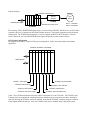
®
E stablished 1981
Advanced Test Equipment Rentals
www.atecorp.com 800-404-ATEC (2832)
APPLICATION NOTE
May 17, 2002
Subject: Generating and Analyzing Wander Using the OTS Product Family
Introduction
This document outlines suggested methods for generating and analyzing SONET/SDH signal wander as part
of an overall Tektronix supplied jitter and wander solution. As such, these procedures utilize the popular
industry standard Tektronix SJ300E Jitter and Wander Generator and Analyzer instrument to supply wander
generation and analysis functions while the OTS9210 module provides the framework around which both
jitter and wander tests may be easily completed. While these procedures describe wander testing methods for
10Gb/s SONET/SDH signals, these procedures may also be applied for SONET/SDH wander at 2.5 Gb/s
using the OTS9300 Multi-rate option.
Test Equipment
The following test equipment and miscellaneous apparatus may be required to perform these tests:
•
•
•
•
•
•
•
Tektronix OTS9000, OTS9010 or OTS9040* test systems equipped with OTS9210 jitter solution.
Tektronix OTS9100 10G or OTS9300 155M/622M/2.5G Transmission Test Solution
Tektronix OTS92S1 Clock/Sync card option.
Tektronix SJ300E SONET/SDH Jitter and Wander Generator and Analyzer equipped with Option 06
(Wander).
A BITS or SETS clock synchronization reference source meeting Stratum 1 clock standards.
A SONET or SDH network element (Device Under Test).
Miscellaneous cables, connectors and adapters as required to interconnect various test configurations.
*Note: The OTS9040 may be used to perform both jitter and wander tests but will require minor OTS
system reconfiguration due to the limited number of backplane card slots available.
Wander Testing Concepts
The proposed wander testing concepts are centered on the capabilities of the SJ300E Wander Analyzer
instrument. Using a combination of the SJ300E Wander Analyzer and the OTS9210 jitter test solution, both
wander generation and wander analysis can be easily performed. The basic wander test concepts used are as
follows:
Wander Generation:
OTS9000
OTS92S1 Clock/Sync
Stratum 1
SJ300E
10 Gb/s Optical Signal
Wander
Generator
Sync
Source
BITS = 1.544 Mb/s
SETS = 2.048 Mb/s
The SJ300E wander generator is used to add wander to a BITS or SETS (Stratum 1) reference signal
connected to the OTS92S1 Sync module, which in turn is used to supply the clock for the OTS91T3 10Gb/s
SONET/SDH transmitter card. This 10Gb/s optical output signal may then be applied to SONET/SDH
network elements for wander testing, i.e., wander tolerance, etc.
Wander Analysis:
Stratum 1
OTS92R1 Jitter Receiver
Wander
Analyzer
Sync
Source
SJ300E
10Gb/s Optical Signal
622 Mb/s Recovered Clock
OTS9000
BITS = 1.544 Mb/s
SETS = 2.048 Mb/s
The incoming 10Gb/s SONET/SDH signal clock is recovered in the OTS92R1 Jitter Receiver card (622 Mb/s
selectable) where it is connected to the SJ300E Wander Analyzer. The wander component is then measured
and analyzed. The SJ300E Wander Analyzer is used to compare the BITS or SETS Stratum 1 reference
clock to that of the recovered SONET/SDH clock signal and provide accurate wander analysis.
OTS System Configuration
The diagram below shows a typical OTS system configured for 10Gb/s jitter and wander measurement
capabilities:
OTS9000, OTS9010 or OTS9040 *
1
2
3
4
5
6
7
8
10Gb/s Optical
OTS91L1 10G Optics
OTS91R2 10G Receive
OTS91T3 10G Transmit
OTS91C3 10G Clock Trigger
OTS92S1 Synchronization
OTS92T1 Jitter Transmit
OTS92R1 Jitter Receive
OTS92H1 Jitter Clock Recovery
*Note: The OTS 9040 mainframe may only contain a maximum of seven OTS cards. The OTS92T1 Jitter
Transmit card is not required for wander generation or wander analysis using these procedures and may be
removed allowing the OTS92S1 card to be installed. Note that the OTS92S1 card must always be installed
in the highest numbered card slot. Only one OTS92S1 card may be installed in any single OTS system.
Caution: OTS slot number versus card placement is not arbitrary. Always refer to the latest Tektronix OTS
configuration guide to ensure card installation is configured properly. The configuration shown is currently
the only allowed configuration for the OTS9010 and OTS9040 mainframes using the cards shown.
Wander Generation Test Configuration
The diagram below shows the SJ300E and OTS system wander generation test connections.
OTS92S1 Clock/Sync
OTS9000
1
2
3
4
5
6
7
8
1.5 Mb/s or 2 Mb/s In
BITS Out
10Gb/s Optical Signal
Stratum 1
SJ300E
REF CLOCK
(Sync)
IN
Sync
Source
L1 R2 T3 C3 H1 R1 T1 S1
OTS91T3 10G Data Transmitter
uses backplane clock source
BITS = 1.544 Mb/s
SETS = 2.048 Mb/s
Configuration details:
1. Access the OTS92S1 card in the OTS GUI and select 2 Mb/s or 1.5 Mb/s external clock option
depending on the reference synchronization signal source used. Note that a 1.544 Mb/s BITS clock
reference signal connects to the small Bantam connector at the bottom of the OTS92S1 card whereas the
2.048 Mb/s SETS reference clock signal connects to the adjacent SMA connector.
2. Using the OTS91T3 10Gb/s transmitter card configuration menu, select the “backplane” timing option.
3. On the SJ300E front panel, select “EXT” as the REF CLOCK synchronization input source. The SJ300E
“Ext” front panel Green LED should be lit. Connect a BITS or SETS synchronization signal to SJ300E
REF CLOCK jack.
4. Access the SJ300E WANDER menu and use the REF SEL option to select the correct signal input type,
i.e., DS1 (1.544 Mb/s), or E1 (2.048 Mb/s).
5. On the SJ300E rear panel, connect the BITS Out jack to the OTS92S1 1.5 MB IN jack. If a 2.048 Mb/s
SETS reference signal is used, connect this reference clock signal to the 2MB/s IN jack. Ensure the
OTS92S1 “Lock Status” indicators are Green. Do not proceed until the OTS92S1 reference clock status
indicators show a successful reference clock lock condition.
6. Connect the OTS91L1 10Gb/s optical output to the DUT (Device Under Test) or in the test configuration
requiring a 10Gb/s wandered signal. Activate the OTS 10Gb/s laser and verify a good 10Gb/s optical
signal is detected by the DUT. This may require selection of a particular 10Gb/s data signal payload
and/or overhead signal to match that required by the DUT, etc.
7. Access the SJ300E WANDER menu and select the desired wander generation signal. Note that
depending on the reference signal used, the choice of wander generation selections vary, e.g., either a
standard TDEV value or industry standard choices. Pressing the SJ300E “Enter” button will activate the
SJ300E wander generator function and “wander” the OTS9000 10Gb/s electrical and optical output
signal.
Notes:
A. BITS clock signal is a DS-1 framed “all one’s” signal at Stratum 1 level accuracy (network
synchronization reference source).
B. SETS clock signal is an E-1 framed “all one’s” signal at Stratum 1 level accuracy (network
synchronization reference source).
C. The OTS9300 “Multi-rate” test option may replace the 10Gb/s test option described above and permit
wander testing at 2.5 Gb/s, 622 Mb/s and 155 Mb/s SONET/SDH rates.
Wander Analysis
Use of the SJ300E and OTS system combination provides a reliable means by which SONET/SDH signal
wander analysis may be accomplished. The diagram below shows the suggested wander analysis test
configuration.
(10 Gb/s testing)
622 Mb/s selectable
Stratum 1
Sync
Source
BITS = 1.544 Mb/s
SETS = 2.048 Mb/s
REF CLOCK
(Sync)
Wander
Analyzer
Recovered
Clock Out
Receiver
Clock In
SJ300E
OTS92R1 Jitter Receiver
Configuration details:
1. Connect the OTS system equipped with OTS9210 jitter option to the SONET/SDH signal to be analyzed.
2. Verify the quality of the received SONET/SDH signal, i.e., error free signal, low SNR, etc.
3. The OTS receiver is normally configured to recover a clock signal from the received signal. Ensure the
OTS data receiver is configured properly. Access the OTS92R1 “Setup” menu and ensure the 622 Mb/s
recovered clock is selected (default option for 10Gb/s signals).
4. Connect a 1.544 Mb/s BITS signal or a 2.048 Mb/s SETS reference signal to the SJ300E front panel
“REF CLOCK” input jack. Ensure the EXT button is Green indicating the clock source is external.
Using the WANDER menu, use the REF SEL option to select the correct clock reference signal type.
5. Connect the 622 Mb/s recovered clock signal from the OTS92R1 receiver to the SJ300E Jitter Receiver
front panel “Clock” jack. Use the front panel SJ300E “Select” button to select the “Clock” jack.
6. Access the SJ300E WANDER menu and using the WAND MEAS option, select “OCN” (line rate
input). Use the front panel “Rate” button to select 622M. Verify a good recovered signal is present.
7. Press the front panel RESET button and use the SJ300E DISPLAY menu to view the current wander
measurement.
Once the SJ300E has been properly configured to analyze wander between the 622 Mb/s recovered clock
signal and the BITS or SETS reference signal, use the various SJ300E wander measurement and analysis
features available to accurately measure and analyze the received signal wander. Refer to the Tektronix
SJ300E SONET/SDH Jitter and Wander Analyzer User Manual, part number 070-9389-02, for specific
details. Note that special software tools are available to assist in this analysis and which requires a serial data
connection between the SJ300E and a PC used to upload and analyze signal wander, e.g., MTIE analysis, etc.
Notes:
A. The wander analysis procedure described above does not require use of either the OTS92S1
synchronization card or the OTS92T1 jitter transmitter card. If an OTS92S1 card is equipped, both
wander generation and wander analysis may be performed simultaneously.
B. Refer to the “OTS Optical Test System 10Gb/s—155MHz Jitter and Synchronization modules” User
Manual, part number 071-1133-00, for additional details related to operating and configuring the OTS
system.
Appendix
SJ300E Wander Analyzer Functional Block Diagram
CLOCK
to Jitter Receiver
51 - 622 MHz
SJ300E
Frequency Divider
Wander Demodulator
BITS IN
(not used)
Clock In
Clock
Recovery
Wander
Receiver
Ref In
REF CLOCK
Ref In
Clock Out
Data
Generator
BITS OUT
Wander Generator
Functional Inputs and Outputs:
CLOCK = SONET or SDH line rate recovered clock signal at 51, 155 or 622 MHz
REF CLOCK = Stratum 1 level network synchronization clock, i.e., BITS or SETS
BITS OUT = BITS or SETS output clock that may be wandered under control of the SJ300E
BITS IN = Used for comparing two reference clocks. Not used in this application
Useful References:
1. “SJ300E SONET/SDH Jitter and Wander Generator and Analyzer”, User Manual, 070-9389-02
2. “Real-Time Wander Analyst Software, SJ300E”, User Manual, 071-0518-00
3. “Performance Assessment of Timing & Synchronization in Broadband Networks”, Tektronix White
Paper (on Tektronix External Web Site)