1
SERVICE MANUAL
Zenith
Local Area
Network
Interface Card (NET-100-1)
Z-100 Series Computers
U
=_",,-"
----'' ' "' ' ' '
~N"H
data
systems
The purpose of this page is to make sure that all servK=e bulletins are
entered in this manual. When a service bulletin is received. annotate the
manual and list the information in the record below.
Record of Service Bulletins
SERVICE
BULLETIN
NUMBER
DATE
OF
ISSUE
CHANGED
PAGE(S}
PURPOSE OF SERVICE
BULLETIN
u.TED RIGHTS LEGEND
ContJactor Is Zenith Data Systems CorpomJon 01 St. Joseph. MIchig8n ..9085. The enllre
doeumenlls IUbject to Umlted Righla data provisions.
Copyrigtt C 1982, 1983 StIIndatd Mlctoeyatema Corporation.
Copyrigl"IICl1984Zenlth Data SyatemI Corporallon,
rightI reserved.
Printed in the UnIted States America
or
z.ntIh on ~ Cofpomlon
8L oIoelIph. . . . . . . . . .
an
INITIALS
Contents
v
Rguree
Tobl
Abbrevlallon
v
vi
SpecIlIc.aUona
Chapter 1
vIII
Introduction
NET-1()().1 Card ...............•....•....•.•....•....•...... _.. _
1·1
Networ\ Operation ••••••....••••••.•••••••.••....•••.•.•..•..•..•..•... 1-2
~
Reoonflguration .....•.••••...•.•.••...••••.•.••••.•.••••••..•.. 1·7
Packet Transfer ............•.••.•.•..•.•.....••..•.•••..•....•..•... 1-7
Transmit .••..... , ......•.•• _..•....••.•.•......•..•....•.•....... 1·7
Receive • . • • . . . . . . . . . . • . . . . • . . . . • . . . . • . • . . . . . . . . . • . . . • . . . . . • • . . . .. 1-7
Parts Supplied ••.• , ••• ,., .•....•.........•......•.. , .•....•....•...... 1-8
Tools Required ............•....•..................................... 1-8
ChlIpIer 2
Hardware and Hoat Comput... Requirement.
Introduc1Ion • •• . .• • . . • . . . . . • . .• . . . . . . . . . . . . . . . . . . . . . . . . . •. .. .
g..100 Bus Pin . . . . . . . . . . . .. . . . . . . . . ..
.
Chaplar 3
2·1
2-1
Dl........b1y
Introduction ...•...•.•.•..•....•.•....•......••••.•..•................. 3-1
O;sassemb~ .. . .. . .. .. .. .. .. .. .. .. .. .. • .. . .. . . . . .. . . .. . .. .. .
3-1
Chaplar 4
Conflguratlon
Introduction • • . • . . . . . . . . . . . . . . . • . • • . . • . • • . • . • . • • • . . • . . . . . . . . . . . . . . . . . . .
TyplcaJ Configuration ....•.......•....•.•..•.•....•.•...................
Detailed Conflguration Data .....•..•.•.•..•.••.•..• ,., .. , •.•............
Jumpers .•. ,., ........•....•••••..•... , .•....•.•..•.•.......•......
4-1
4·1
4·3
4-4
Switches ....................•....•.•..•......•......•.............. 4·5
ChlIpIar 5
Inatallallon
IntrodLIction ..•........................•..••..• , . • . . . . • . • . . . . . • . • • • . • • . 5-1
NET-1QO-1 card Installation •.•••••...•... , .••...•.•..•••..........•..... 5-1
Network Chassis Adapter Installation
5-2
Chaptar 8
Inllial Ta.ta
Introduction .......•....••.•.••.•.•....••...••••...••..•........•• , . . . •
RAM Test ..•.....••..•......•.•..•..•.•.......................•......
110 Test •••..•••.•••.•....•....•....•.•....•......•.•......•.••.••..•
Memory Test .....•••••.•.•..••••••....••••• ,' •.••••••..........•.....
Chapter 7
e.1
e.1
6-2
6-3
_ _mbly
introduction •••.•.•.•.••....••.••••.•.••.•••••...•••. , .......•.•••••..• 7·1
..........bIy •.••.•••••.•..•••..••••••••.••.••.•••.••............•.....
7·'
Page
iv
Contents
TMory of OpenIflon
Ch8pler 8
introduction ••....•...••..••...•.••••....•••.•..•...•..•............. _. 8-1
Bus Buffers •...•..•••••••.......•.•..•.•..•.••.........•••.•..•..••• 8-2
Multiplexers (MUX) .•.•.••.•.••...•••••••.•..•••••...•••.•..•••••..• __ 8-2
System Decode and Con1rol... . . . . . . . . . • . . . • . . • . . . . . . • . . . . . . • . . . . . . . . . 8-2
Wait Generation ••••••••.•.••.... _..•.. _. . . • . • . . . . • . • . . • . . . • . . . . . . . . . 8-2
Read Only _
(ROM) ••.••.....••••••.••.•...••••.•.•.••••.•..•.. 8-3
Random Access M8I1lOry (RAM) .....••.••. _••••..•.•.•..•.•........... B-3
Network Controller •••••••••••... _...•....•......•......•.•.••.•...... 8-3
10 Number .......................•.••.•..•••....................... 8-3
Active Hub
8-3
Circuit IlacrIptlon
Ch8pter 8
Introduction .••......•.•......•.••.•••••• _•• _.••..........•......•...• _ 9-1
Bus Buffers __ ...•..••••.•••••..•.•..••••.•.......•••.••.•••..•.•..... 9-1
MuItlpIexers ••....•••.•••••....•...••...•.•....•.•....•.•..•..••...... 9-1
ce>t.9>26 Intertace (U118) •••....•..••••••.••••••.•••.••.••••...•••..•.• 9-1
System Decode and Con1rol .........•...••.•.•.•..•.•....•.•.•..•......
,
_
.................•....•. ~
&-bit Addressing
Interrupt
Phantom
9-2
2
9-3
9-3
9-4
Wait Generation •...•.•••••.••••.•••••..•••..•.••••....•.•.•.•••••..... 9-4
ROM Circuitry ........••.•....•....•...••••.•.•••..•.••.•...•.••...... 9-6
RAM Interface
,
,
9-8
Network Controller ........•.•..•..•.••.•••.•..•••....•••....•.•.•...... 9-9
10 Number •.•........••••.•..••••••••••••...•.....•... " ••.•. , •.•.... 9-9
Active Hub. . . .
. ..••.••..•.•..•.•..•.••...•..•.............••...•. 9-10
Ch8pIe, 10
Service Instructions
Introduction .....•.•.•..•.••.•.•••.••.•••.••......•...•..••.. " ..•.••. 10-1
TroubIeshooIing ........•....•......•...•..•.......................... 10-1
ChlIp!er 11
Perla U81
IntrOOJction ................•..•.•••••..•••••..•..••••••.•.....•...••• 11-1
Replacement Pans ••••••...• " ...•.•....•.•.....••.•.••••..• " ......• 11-2
NET-l00-1 Network Card .... , ...•.•..•.•.•..•.•........•... " ••..... 11-3
NetwOrk Chassis Adapter .....••••••..••..•...•..•..• , •••........•... 11-6
Semiconductor IdentifiCation ...••...•.•....••.•..•...••...••••••.•...... 11-8
Part Number Index ••........•....•......•....•.•. ,
,
11-8
PALEqualions •.••.•.•••......••••••.•••.••..••..••..•...........•.. 11-15
ChlIpler 12
Dele
_Ie
Introduction ..•.••••••••••..••••.•••••.••..•..••••••••••..•..•••.••..• 12-1
Data Sheets - C0M9026 Local Area Netwotk Controller (lANC) .•••••.•..•• 12·2
-
CQM9032 Local Area Network Transceiver (LANT) .•.•••.••. 12-16
Page V
Contents
~I.A
10 _
Number Lockup T _
Figures
1-'
ZlAN Topology ................•........................•...... '-2
1-2
Dalsy ChaIn Conriguratlon ..••..... _. . . • • . . . . . • . . . . • . . . . . . • . . • . .. 1·4
Tree Configuration •.••.•......• , ....••••....•.•..••..•.•••...... '-5
logical Netwol1( •••••••••••••.•••... _ •.••.••.••.•....•.......•.. '·6
DisassefnbIy, A1Hn-()ne Model ......•.......•....•...••..•.•..... 3-1
1-3
,-4
3-1
3-2
....,
....2
4-3
5-1
5-2
7-1
7-2
8-1
9-1
9-2
i-3
11-'
11·2
DisassefnbIy, Low-Profile Model .....••••••.••.••••••............. 3-2
Typical ConfIguration ••.••••.•..•.•..•.•..•.•....•....•.......... 4-1
Configuration Jumpers
_
_. . • . . . . . . . . .. •.•........ 4-3
Configu<ation _
...•.•...........•.•...••.•.••.••.•.•.....
4-.
NET 100-1 card Installation ............•.•..............•....... S.1
Network Chassis Adapter Installation _....•......•. __ .• _..••.•..... 5-2
Reassembly, AII-ln-<>ne Model
_. _•....••....... __
_. 7-1
Reassembly, Low·ProMe I.'Odel .•...........•.•.•..•....•......... 7-2
NET-1 00-1 8Iodl: Diagram •.•.........•....•.•....•.•.••.•.•..... 8--1
_
" " " - ' •••••.••••••. ~ ~ .•..••••••••. ~ .•••.••••.... ~ ..• ll{l
TOlTirlg Diagram
...
~ Insertion . • . • • • • . • . • • • • . • . . . . . . . . . . . . . . • . • . . . . • . . . • • . . . . .• 9-6
Component V
NET 100-1 Card
11-2
Network Chassts Adapter Exploded VIeW ........•.•....•....•..... 11·7
Tables
.1
10-1
ROM Jumper Configuration ......••••.........•....•...•.•......• 9-7
Troubleshooting ......•..•......•.•....•....•....•.•..•.•...... 10-1
Page
vi
Abbreviations
ACK
ADIE
AS
BINP
BMEMR
BOUT
BSYNC
CE
ClK
CR
DBIN
DID
DIP
DIS
EN
EDT
ESDS
ET
lED
IDDAT
IDLD
110
ILE
1M
10ADRS
10REO
10
INTR
LANC
LANT
MASM
MEMADRS
MEMREO
MUX
NAK
NID
DE
Acknowledgment
Address'llata Input Enable
Address Strobe
Suslnpul
Sus Memory
Bus Output
Bus Synchronization
Chip Enable
Clock
Carriage Retum
Data Bus Inpul
Destination Identification Number
Duallnline Pact<
Disable
Enable
End Of Time
Electrostatic sensitive Devices
Extended Timeout
Ugh! Emitting Diode
10 Data In
10 load
Input/Output
Interface latch Enable
Interface Module
Input Output Address
Input Output Request
Identification Number
Interrupt
local Area Network Controller
local Area Network Transceiver
Macroassembler
Memory Address
Memory Request
Multiplexer
No Acknow\edgment
Next Identification Number
Output Enable
Page vii
Abbreviations
PAL
PR
PRSFF
PULS
RAM
ROY
REO
ROM
ROMSEL
RX
510
TX
WE
ZLAN
Programmable Array logic
Preset Lines
Preset Flip-Flop
Pulse
Random Access Memory
Ready
Request
Read Only Memory
ROM5elect
Receive
Source Identification Number
Transmit
Write Enable
Zen~h Local Area Network
Page viii
Specifications
Buller RAM SIze . . . • . . . . . . • • • . .
2K x 8(6116-4)
ROM Size OptIonl . . • . • . . . . • • . . .
4K x 1 (2732-2)
8K x 8 (2764-2)
16K x 8 (27128-2)
I/O Add.....lng . • . . . . . . . . • • . . . .
Jumper selectable 8·b~ or 16-~ addressing
IIImory Add....lng . . . . . . . . . . • . .
Jumper selecteble 16-M Of 24-b~ addressing
Maximum Dlltence - - . Units . . • • .
2000leeI
Maximum _
Per Syltom ••••••••
255
InllrrUpl Operation • • . . . . . . . . • . . •
Jumper seIecteble VIO"·Vlr, NMI, end INT"
Local Area Network Controller . . . . . . .
SMCCOM9026
Local Area _ork Interf8ce . . . . • • • •
Zenith Hybrid EGA0591 02A
RAM/VO ACCllllI TIme • . . . . . . • • • . •
880 os maximum
1_ ................
ROM Acce.. Time . . . . . . . . . . . . . .
220 ns maximum
Coble
RG62A Coax, 93 Ohma BNC Connector
Bu. Interface . . . . . . . . . . . . . . . . .
5-100,IEEEStanderd696
_
8-11 volts DC
TypiceI1.6A. Maximum 2.0A
-12 vohs DC et.03A
Requirements • • • • • • • . • • • . •
Chapter 1
Introduction
This chapter introduces the NET-llJO.l Card, Zenith LocaJ Area Network
(ZlAN) operation, parts supplied, and the tools required lor installation.
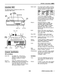
NET-100-1 Card
The NET-1 lJO.1 Card is a IocaJ area networking card compatible with Data
point's ARCNET System. It will allow the Z-l00 Compuler to inteflace
with up to 255 similarly configured compulers, a1 a maximum distance
012000 teel. An active 4-por1 hub is incorporated on the NET-1lJO.l Card.
A local area network can be set up by daisy chaining or with the hub,
using the approprtate software. This card is supplied fully populated, and
may be placed in any vacant card slot in the computer.
The active hub requires all unils in a path or trea to be po_ed up for
the system to communicate property.
The card can be configured in many ways with the available swilches
and jumpers. This capabilily is especially useful for configurtng the memory
on the card around system memory. Yet, the card can be used as supplied,
fully configured except lor the 10 number. The 10 number is a swilch
set to the desired 10 number. Reier to appendix A for number selection
and conversion.
All 01 the information needed to use the features of the NET-1lJO.l Card
is contained within this manual. Please reed it carefully before attempting
tousetheNET-1lJO.l Card.
Page
1-2
Introduction
Network Operation
ZLAN consists of a token·passing scheme. where each node (unit) passes
to the next active higher 10 number an invitation to transmit Up to 255
unique node numbers may be assigned to a ZLAN network (refer to Ftgure
1-1),
figure 1-1. ZLAN Topology
Page
1-3
Introduction
Reterto Figure 1-1 for the following example.
EXAMPLE: Node 4 desires to communicate to node 20. The interconnecting nodes must be powered on because the board has an Betive-hub.
Nodes: 2, 3, 4.7, 11, 12, 16, 17, 16, 19, and 20.
The network can be configured in two ways. Each has advantages and
disadvantages which depend on the system to be installed. For the highest
efficiency networK, determine which configuration is best for the system.
Figure 1-2 shows a daisy chain configuration. The main advantage of
this configuration is that a unit may be easily inserted into the system,
keeping cable runs at a minimum. The disadvantage of this system is
that all units must be powered on for communications to occur.
For example, a network system is set in a company where 5 of 20 units
are, at times, inaocessible to the other users. Using a daisy-chain config~
uration, the entire system will not be able to communicate if any unit
Is powered down. Without access 10 5 compulers, those physical lines
must be bypassed, (if this is even possible) for the network to communicate. This is an undesirable situation which can be avoided by using the
tree configuration.
Rgure 1-3 shows a basic tree configuration. Set up in branches, this configuration does not require all systems to be powered on for communication
to occur, just the individual branch must be active. The main disadvantage
is that the tree configuration does require prethought on wiring. Possible
future sites should be taken into consideration while connecting the system, when using the tree configuration.
In the tree configuration, the unaccessible 5 computers can be set in a
separate branch, allowing the network to communicate without these units
powered on.
Although these configurations may look unique, the logical network is the
same, as shown in Figure 1 ~4. Do not connect the network in this manner.
Use only a daisy chain or tree configuration.
Page
1-4
Introduction
,,'
,ARCNET SYSTEM
(OPTIONAL)
,~' , " ,... ARCNET
...~,
ARCNET-__
SYSTEM
8
[p~)r-'
it
,,;
SYSTEM
...
-'
ARCNET
SYSTEM
FIgu... '-2. DIlley ehllin Conflgurdon
Page
1-5
Introduction
ARCNEr
SYSTEM
ARCNET
SYSTEM
ARCNET
SYSTEM
ARCNET
SYSTEM
ARCNET
SYSTEM
ARCNET
SyaTEM
ARCHET
ARCHET
ARCNET
SYSTEM
SYSTEM
SYSTEM
F1gu.. l-3. Tree Conllgumlon
Page
1-6
Introduction
7
figure 1-4. Loglcel_
Page
1-7
Introduction
Network Reconfiguration
At network reconfiguration time, all 10 numbers, up to 255, are polled.
Each node will remember the next 10 number (NID) the token was passed
to. In this way, the token will be passed only to active 10 numbers, preventing wasted time. Every time a node is powered up in the network, a network
reconfiguration will occur. The network reconfiguration (consisting of eight
marks and one space repeated 765 times) will destroy the token and
prevent another node from taking control of the network.
When a node is powered down or disconnected, there is no need for
a network recontiguration. When the preceding node does not receive
a response from its invitaton to transmit, it will increment the NID it has
stored and send another invitation to transmit. The node will continue
to increment the NID and retransmit until a response is received from
an active node.
Packet Transfer
Transmit
When a node receives the token and it has a packet or message it wants
to send, it looks at the destination 10 (DID) and sends a free buffer inquiry
to that 10 (~ the DID is 0, it signifies a broadcast to all nodes). If the
DID responds with an acknowledge (ACK), the node will send the packet.
If there is no acknowledgment (NAK) or ACK is not received after 74
microseconds, the node will pass the token to the NID.
Receive
The node receiving a free buffer inquiry checks the receiver inhibited flag.
" the flag is set, an NAK is sent to the source 10 (SID); ~ not, an ACK
is sent.
Page
1-8
Introduction
When a packet is transmittad, the raceiving node first writas the SID into
~s receive buffer. Next, ~ will look at the DID. If the DID is neither 0
nor its 10 number, the node will ignore the rest of the packet.
" the DID corresponds to the raceiving node's 10 number, the node will
send an ACK to the SID, set the receiver inhibftad flag, and write the
packet into its receiver buffer. For a broadcast (D10~O), the node will
store the packet in its receive buffer If broadcast reception is enablad.
"not enablad, the node will ignore the rast at the packet.
Parts Supplied
The following palls are supplied in this interface card package:
•
•
•
•
NET-100-1
NET-100-1
(2) 6-BT x
NET-100-1
Card
Chassis Adapter
.375" SCrews
USER'S MANUAL
The following accessorias are optional:
•
•
HCA-60 - 25 loot coax cable.
HCA-61-100footcoaxcable.
Tools Required
The only tool_ requirad for the installation of the NET-100-1 Cerd are
a small flat blade scrawdriver and a small Phillips scrawdriver.
Chapter 2
Hardware and Host Computer Requirements
Introduction
The NET-1QO-1 Card uses the S-l00 Bus Interface, IEEE Standard 696.
Therefore, computers used with this card must meet the same standard.
Usted below are the 5-100 Bus pins used, signal, type, and their active
level.
5·100 Bus Pin
PIN NO.
4
5
•
••
7
10
11
12
SIGNAl.ITYPE
ACTIVE LEVEL
VOO' (5)
VI1" (5)
W' (5)
V13' (5)
L
L
L
L
VI4"(S)
VIS' (5)
VI6' (51
vir (5)
NMI' (5)
L D.C.
H
H
H
'5
A18(MI
1.
17
20
24
A18(M)
A17 (M)
29
30
31
M(MI
MIM)
A3IM)
A1S(M)
A121M)
32
33
GNO(B)
01 IB)
36
37
38
,,"(M)
00' (M)/OATA' (MIS)
000 (M)/OATAO(MlS)
A101M)
004 (M)IDATM (MIS)
39
40
41
DOS (M) IDATMIMlS)
006 (M)IDATA6 (MIS)
012 1M) IDATA10 (MIS)
34
35
D.C.(lDwopenool_)
D.C.
D.C.
D.C.
lO.C.
L C.C.
l C.C.
l D.C.
o Volts Une
"
H
H
H
H
H
H
H
H
H
H
H
H
H
Pago
2-2
Hardware and Host Computer Requirements
PIN NO.
SlGNAlJTYPE
ACTIVE LEVEL
H
H
42
DI3(M)IDATA11 (MIS)
43
017 (M)/DATA15 (MIS)
45
sOUT(M)
slNP (M)
sMEMR{M)
GND(8)
+8 VoltS (B)
46
47
50
51
52
-16 Volts (8)
53
GND (8)
Al9IM)
A20IM)
A21 1M)
59
61
62
63
64
67
70
72
H
H
H
OVollsUne
o Volts Une
H
H
H
A22 (M)
A23IM)
PHANTOM" (MiSI
GND(8)
ADY (5)
H
H
INTO IS)
AESEr (8)
lO.C.
o Volts Une
H O.C.
73
75
76
pSYNC(M}
78
pWAO(M)
pD81N 1M)
L D.C.
L D.C.
H
L
H
AO(M)
A1 (M)
A2IM)
A8IM)
A7IM)
H
H
H
H
H
AaIM)
A13(M}
A14(M)
All(M)
D02 (M) IDATA2 (MIS)
H
H
H
H
H
003 (M) fDATA3 (MIS)
007 (M)/DATA7 (MIS)
014 (5) IOATA12 (MIS)
015 (S)/DATA13 (MIS)
016 (S)IDATA14 (MIS)
H
H
H
H
H
95
DI1 IS) /DATA9 (MIS)
010 (5) IDATAB (MIS)
96
sWO· (M)
100
GND (8)
H
H
L
DVottsUne
n
79
80
81
82
83
84
85
88
87
88
.,
89
90
92
93
94
Chapter 3
Disassembly
Introduction
This chapter provides the information to remove the top of the Z-100 Computer for NET-100-1 Card installation.
WARNING: Dangerous DC voltages are present inside the computer. Be
sure the line cord is disconnected.
Disassembly
AII-ln-Cne
_1- Refer to Figure 3-1 and complete the following steps.
1.
Unplug lhe line cord lrom the AC outlet.
2.
Using a small flat blade screwdriver, move the metal slides all the
way 10 the Iront and then 1W to the back as shown.
3.
Carefully Iill the top case straight up and set lito one side.
CA SE
-----
Flgure3-1.
---
Dl.........bly.AII-ln-One-.
Page
3-2
Disassembly
Low Profile _
steps_
-
Refer 10 Figure 3-2 and camplele the following
I.
Unplug the line cord from the AC outlet.
2.
Pull Ihe metal slides all Ihe way 10 the back, and then push Ihe
metal slides 1/4" to the front. as shown.
3.
Carefuly lift the top case straight up and sal it to one side.
FIgure 3-2.
Di........ bly. Low-Proflle_1
Chapter 4
Configuration
Introduction
This chapter describes the typical factory configuration used with the Z-1 00
Computer. Detailed configuration information is furnished for Z·100 users
who desire to modify or customize their configuration, and non-Zenith Data
System microcomputers with 8·100 Bus compatiblity.
Typical Configuration
The following is the typical board configuration which is preset at the factory. Refer to Figure 4-1 while reading this section.
CAUTION: This product contains ESDS (electrostatic sensijive) devices.
Exercise normal caution in handling these devices to prevent static discharge damage.
Figure 4-1.
Typical Conllgur.tlon
Page
4·2
Configuration
•
Programming jumper across JI 01, pin 5 (V12' inlerrupl).
•
Programming jumper on JI05, pins 2 and 3 (righl) (8-bil VO addressing).
•
Programming jumper on JI07 and JI08, pins 2 and 3 (right), and
JIOQ, Jl1O, and JIll, pins I and 2 (left) (test points on COM9026
chip).
•
Programming jumper on JI12, pins I and 2 (left), and JI13, pins 2
and 3 (righl) (2764-2 ROM).
•
DIP (Dual Inline Pack) Sw~ch SWIOI positions 0 - 3 10 !he ON (0)
position and all others to the OFF (I) position 10 select OFooooH lor
the RAM addre...
•
DIP Sw~ch SW102 positions 0, I, 2 and 3 to the OFF (I) position
and all others 10 the ON (0) posilion to select OF4000H for the ROM
address.
•
DIP Switch SWI03 posilions 0 and 2 to the OFF (I) position and
all others to the ON (0) position to select ooAOH for Ihe I/O address.
•
Dip Switch SW104 position 6 to the OFF(I) position and all other
positions to the ON (0) position.
•
DIP Switch SW105 is the 10 number switch. Set Ihis to the 10 number
you desire. (Each unit in the system must have a unique 10 number.)
For example, ror 10 number 100 (64H), set positions I, 2 and 5 10
Ihe OFF (I) position and all others to the ON (0) posilion, as shown.
Refer to appendiX A for cross reference to other 10 numbers and their
respective positions.
POSITION
ON/OFF
01234567
ON OFF OFF ON ON OFF ON ON
NOTE: To insure proper setting refer to memory test in Chapter 6.
•
Dip Switch SWI 06 all positions 10 the ON (0) position.
•
Dip Switch SWI 07 an positions to the ON (0) position.
Page
4-3
Configuration
Detailed Configuration Data
The following informetion is furnished to configure the NET-lllO-l Cerd
for non-Zenith Data Sys1em S·l00 Bus compatible microcomputers, as
well as for the Z-100 user who desires to make modifications or effect
a customized oonfiguration.
CAUTION: This product contains ESDS (electrostatic sensitive devices).
Exercise normal caU1ion in handling these devices to prevent static discharge damage.
Refer to Figure 4-2 for the locations of the jumpers.
,
•
1~
-
•
~,
-
IBiD
WUI:
-
Figure 4-2.
,~
Configuration Jumpen
Page
4-4
Configuration
Jumpers
J101 - Selects the interrupt on the S100 Bus. Only one of the following
should be jumpered.
NMI'
INT'
VIO'
V11"
V12'
V13'
V14'
VIS'
V16'
vir
J1 OS -
For 16-bn addressing pins 1 and 2 are jumpered; for 8-bit addres-
sing, pins 2 and 3 Bfe jumpered.
J107 (T2) - Jumper pins 2 and 3 for nonnal COM9026 operation. When
pins 1 and 2 are jumpered, chip level testing can be pertonned.
J108 (T1) -
Jumper pins 2 and 3 for nonnal COM9026 operation. When
pins 1 and 2 are jumpered, chip level testing can be performed.
J109 (ECHO) - Jumper pins 1 and 2 for nonnal COM9026 operation.
When pins 2 and 3 are Jumpered, COM9026 will retransmit all messages
less than 254 bytes.
J110, J111 -
These two jumpers specify the time-out durations as follows:
ET2
ET1
RESPONSE
TIME (us)
RECONFIGURATION
TIME (ns)
1
1
0
0
1
0
t
0
74.7
283.4
561.8
1118.6
840
1680
1680
1680
Page 4-5
Configuration
J112 -
When using a 27128 ROM, jumper pins 2 and 3. For other size
ROM's. jumper pins 1 and 2.
J113 - When using a 2732 ROM, jumper pins 1 and 2. For 2764 or
27128, jumper pins 2 and 3.
J114 -
When pins 2 and 3 are jumpered, the EPROM will not cause
PHANTOM" to be active. When pins 1 and 2 are jumpered, PHANTOM"
will be active when the ROM is seleeted.
J115 -
When using a 2732 ROM, jumper pins 2 and 3. For a 27128,
jumper pins 1 and 2. For a 2764, no jumper is required.
Switches
Refer to Figure 4-3 for the location of the switches. In the following configurations, OFF equates to a logic "1", and ON to a logic '0".
,......
.-
If'''~:lll .~
•
~.,
. it
._.-...
.., .~~
!*I:lUijtH:lj , _ l:ll:l'dl:IltiJU : li.i'
'.
I
.
I
Figure 4-3. Conllguratlon 5wllc....
,u:
Page 4-6
Configuration
SW10l - This switch. in conjunction with SW106. selects the memory
address location for the RAM. For example. to select the address OFOOO
(HEX). SW101 would have the folloWing configuration:
01234567
POSITION
ADDRESS BIT A23 A22 A21 A20 A19 AlB A17 Al6
ONIOFF
ON ON ON ON OFF OFF OFF OFF
SW102 - This switch, in conjunction with SW104, selects the location
01 the ROM. For example. to select the address OF4000 (Hex). SW104
would have the folk>wing configuration:
POSITION
0
1
2
3
4
5
ADDRESS BIT A16 A17 AlB Al9 A20 A21
ON/OFF
OFF OFF OFF OFF ON ON
6
7
A22 A23
ON ON
SW103 - This switch. in conjunction with SWl07. selects the 1/0 address location. For example. to select OOAO (HEX). SW107 would have the
following configuration:
POSITION
o 1
ADDRESS BIT A7
A6
ON/OFF
OFF ON
2
3
A5
A4
OFF ON
4
A3
ON
5
A2
ON
6
Al
ON
7
NC
X
SW104 - This switch, in conjunction with SW102, selects the location
oflhe ROM. OF4000; SW104 would have the following configuration:
POSITION
0
ADDRESS BIT NC
ON/OFF
X
SW10S -
1
NC
2
NC
3
4
NC
NC
X
X
X
X
567
A15 A14 A13
ON OFF ON
This switch selects the ID node number. There should be a
unique node number for every unit in the network. When position 7 is
set OFF and all other positions ON. the ID node number is 1. When position 6 is set OFF and all other positions ON, the node number is 2, etc.
The following settings win select ID node number 114 (72H):
POSITION
ON/OFF
01234567
ON OFF OFF OFF ON ON OFF ON
Page
4-7
Configuration
NOTE: This 114 number is different from the typical configuration to provide another example of 10 number selection.
NOTE: To insure proper setting refer to memory lest in Chapter 6.
SW106 - This switch, in conjunction with SWl 01, selects the MEMADRS
Iocation,OFOOOOH.
POSITION
0
1
2
3
4
ADDRESS BIT A15 A14 A13 A12 All
ON ON ON ON ON
ON/OFF
SW107 -
5
6
7
NC
NC
NC
X
X
X
This switch, in conjunction with SW103, selects the IOADRS
location.
POSITION
ADDRESS BIT
ON/OFF
0
AS
ON
1
2
A9
Al0 All
ON ON
ON
3
4
5
6
7
A12 A13 A14 A15
ON ON ON ON
Chapter 5
Installation
Introduction
This chapter provides the necessary information to install the NET·l00·1
Card and Network Interface.
NET·100·1 Card Installation
CAUTION: This product contains ESDS (electrostatic sensitive devices).
Exercise extreme care in handling these devices to prevent damage.
Refer to Figure 5-1 and complete the following steps.
1.
Select a vacant card slot in the card cage assembly.
2.
DisconnectS inch disk drive cable (134-1264), ffused.
3.
Insert the NET-100-1 Card, with the components facing forward, into
the selected card slot Seat the card firmly by pushing straight down.
Figure 5-1.
NET 100-1 Cerd Inl!llilalion
Page
5-2
Installation
Network Chassis Adapter Installation
Refer to FlQUre 5-2 and complete the steps below.
6-Bld/."
SELF-TAPPING
\..
'0
SCREW
Allure 5-2.
Network C!IlIul. Adapter I n _ l _
Page
5-3
Installation
,.
Choose two of the adjecent unused 25 D·pin connectors on the beck
panel. We suggest J5 and J6 connectors. Remove the hole plug
buttons which cover these holes and discard them.
2.
Carefully sand or scratch the paint off tha back panel from tha two
outermost screw holes.
3.
Place chassis adapter over these holes and feed the cables through
the holes to the inside of the unit.
4.
Using two HE 250-1434 (6-BT x .375) self-tapping screws, fasten
the chassis adapter to the rear panel.
5.
Connect the cables fed to the inside of the unit 10 the NET· 100
board connectors PI 01, Pl02, and P103. The connector has three
pins, but only two contacts are used. The outer pins contain the same
signal and the contact may be installed either way, as long as the
middle pin makes contact with the middle connector.
This completes tha installation of the networK chassis adapter. To connect
nodes together, RG62 coaxial cable can be run through ceilings, on floors,
or along the walls. For shorter delays and less cabling, keep long runs
to 8 minimum.
CAUTION: Since other installations may use similar cable and connectors,
be sure tha correct connectors and cabling are connected to tha NetworK
Chassis Adapter, Damage to this board may result if improper connections
are made.
Chapter 6
Initial Tests
Introduction
This chapter contains three inilialtests to make sure the NET-100-1 Card
is property operating and interfaced to the system. The three tests are
RAM, 110, and Memory.
NOTE: These tests are interrupted by pressing the CTRL and RESET
keys simultaneously.
RAM Test
The following is a test routine to detennine ij the RAM is opereting property.
Using a wor1< processor program or EDLIN, enter the following under file
RAM.ASM.
'QU
OFOOOH
GROUP
GROUP
ASSlIlE
S_
DSEC, STACK
O,O,OFFH
DSEG
OS
ENIlS
STSEG
SEQIOO
STACK
2S6DUP (? )
DSEG
DATA.JlUITEllO
DB
STSEG
CS,",
INITJOlST:
csoo
CS:CQlOO!', DS:DGROU1'. SS:DGROU1', ES:NCllUNG
ENDS
SEQIOO
PUSH
I'USH
AX
BX
PUSH
ex
I'USH
IIlV
MaV
OX
AX, DGROU1'
DS, AX
MOV
IIlV
AX, NET..lIEI.ADRS
ES, AX
IIOV
BX, 0
NOV
AL, 0
INlTJltlFFER:
Poge 6-2
Initial Tests
LOOP:
IIlV
JIIP
ES: I BJ( I. AL
POP
POP
ox
POP
POP
RET
LOOP
ex
BJ(
AX
ENDS
00
Type
Type
Type
JL\SII
LlIIX
RAI
RAI.ASI
RAI
LED 0105 should light while this test is being performed. If LED 0105
does not light, referlo Chepter 10. Service Instructions.
I/O Test
The following Is a test routine to determine if the VO network is operating
properly. Using a word processor program or EDLIN, enter the following
under file IO.ASM.
STSEG
EQU
OOOAOH
GIlOUP
GIlOUP
ASSlIlE
DSEG, STACK
SEGIIOO
STACK
DB
256DUP I? I
CSEG
cs: CCIlOOP, OS: 1lGROOP, SS:IlGROOP, ES:NOl1Ilt(;
ENDS
SEQIlIT
PUSH
PUSH
BJ(
AX
PlJSH
ex
PUSH
IIlV
II)V
OX
AX, IlGROOP
OS, AX
Page 6-3
Initial Tests
lIOV
IN
AND
ClIP
JE
lIOV
lIOV
JIlP
CSEG
OX, NET.ID.AORS
AL, OX
AL,OI
AL, 0
LOOP-TA.O
DX, NET_IQ.ADRS + 1
AL, 003H
LOOP.'l1\ANSllIT
pop
pop
ex
POP
BJ(
pop
RET
AX
DX
ENDS
END
Type
Type
llASII IUSII
LINl 10
Type
10
LED 0102 should light while this lest is being performed. If LED 0102
does not light, refer to Chapter 10. service Instructions.
Memory Test
The purpose of this lesl is 10 delermine ~ the RAM and its interface to
the system are operating properly. If a difficulty is ancountered while this
test is being performed, reler to Chapter 10, Sarvice Instructions.
1.
Tum on the computer and monitor.
2.
After the prompt type EFOOO:O (the monitor will show Examine
FOOO:O) RETURN.
Thelollowing should be displayed on the monitor:
FOOO:OOOO 01 = RETURN
Page
6-4
Initial Tests
Now FOOO:OOO1 64 = should be displayed, 0< the 10 node number
set by SW105 in He•. This number will differ depending on the 10
number your board is set for. RETURN
3.
When the memory location is given on the screen, type the number
listed below. After every entry hit a carriage retum to advance to
the next memory location.
ONSCREEN
TYPE
FOOO:0002
FooO,0003
FOOQ,0004
"
rooo:ooos
•
FOOO,0006
Fooo,0001
fOOO:OOO8
FooO, 0009
rOOO:OOOA
FOOO:OooB
FOOO;OOOC
FOOO,OOoo
FOOO:OOOE
FOOD: Door
FOOO:OOIO
4.
,•"
A
B
"o
,.
Hit the DELETE key to get the prompt back.
The following should be displayed, indicating that lhe RAM
written to and read from,
can be
FOOO: 00000164 01 02 03 04 05 06: 010809 OAOBDCODll£
fOOO: 0010 OF
NOTE: FOOO:OOO1 should read the 10 node number in he. set by SW1 OS.
Chapter?
Reassembly
Introduction
This chapter contains the information required to install the top of the
Z·100 Computer after NET·100·1 Card installation, configuration, and
tests.
Reassembly
AJI~n-One
Model -
Refer 10 Figure 7-1. Connecl cable (134-1264), ij
using 8·inch disk drive. Replace the lOp case by bringing it straight down
into its position. Using a small flat blade screwdriver, slide the latches
all the way to the front.
This compJetes the reassembly of the all-in-one model.
figure 7·1. R_oembly, All-In-One Model
Page
7-2
Reassembly
Low-Proltle Model -
Refer fo Figure 7-2. Connect cable (134-1264),
if using 8-inch disk drive. Replace the fop case by bringing n straight
down into its position. Push the latches all the way fo the front.
This completes the reassembly of the low-profile model.
fTOPi
~
Chapter 8
Theory of Operation
Introduction
ThiS chapter provides a brief explanation of the theory of operation of
the NET·100 Card. If a more detailed theory of operation is desired. refer
to Chapter 9, Circuit Description. Refer to the block diagram, Figure 8-1.
as you read the following description.
",
IlUFFER$
I
I
•,
0
••
••<"
•
•
·
MULTI"lEX"-RS
<C-
-
0
<
<
•"
•e
•
•<"
"
••u
•
e
•
'"
I
CnASSIS ... nAPiOR
t IINC CoN"ECTOFl l
---'l
SVSlEM
nEcooE
•,
'"
NEfWORIC
COIHROl.lE"
CONTROL
'fI'AIT
GENERATION
~
I
'Q
o.
;=:
""'
I
.au
J l) l
Rgure &-1.
flGUA
ACTIVE
NET-1C»-1 Block DI8lIrem
~
COAX
C"'BLE
Page
8-2
Theory of Operation
The NET-100-1 Card is divided into nine main sections.
•
•
•
•
•
•
•
Bus Buffers
Multiplexers
System Decode and Control
Wait Generation
Read Only Memory (ROM)
Random Access Memory (RAM)
Network Controller
•
10 Number
•
Active Hub
The following paragraphs describe each of these sections.
Bus Buffers
The bus buffers Bre receivers and drivers for the 5-100 address, data,
and control signals.
Multiplexers (MUX)
The addresS/data multiplexers pass the a-bit address onto the internal
IADO-IAD? bus line to the networl< controller. The S-bit data is then passed
to the controller in the same way.
System Decode and Control
The system decode and control circuits contain all the logic necessary
to control memory and 110 accesses, 8 and 16-bit data transfers. interrupts,
and phantom assertion.
Wait Generation
The wait generatkm circuitry receives the network control wait signal and
transforms it to the 5-1 00 ready signal.
Page
8-3
Theory of Operation
Read Only Memory (ROM)
The ROM allows the capability of booting in a non-disk environment. The
support circuitry provides a 24-bit, switch selectable location in memory
(phantom control optional through a jumper). The board does not come
equipped with the ROM installed.
Random Access Memory (RAM)
The 2K x 8 RAM can be accessed by both the nelwor!< controller and
the system processor. The RAM location in memory is 24-bit, switch selectable on 2K boundaries.
Network Controller
The network controller provides the necessary interface between the S100 Bus and the network. tt controls waits, interrupts, and data to and
from the system.
IDNumber
The 10 number is a unique number from 1 to 255 gIven to every node
(unit) in the nelwor!<. Physically set by an onboard switch. n serves to
identify where a message is generated, where the message Is being sent,
and the priority that unit has.
Active Hub
The active hub decodes and encodes the incoming and outgoing
mes~
sages. The hub allows implementation of a small network without any
external hardware through the available three ports. The fourth port is
dedicated to the network controller; no external connection may be made
00 it.
Chapter 9
Circuit Description
Introduction
This chapter provides a detailed circua description of the NET·1()().1 Card.
Refer to the schematic diagrams for the following discussion.
Bus Buffers
Ul01, Ul02. Ul08, and Ulll are the address bus buffers. Ul03 is the
buffer for the data out ([)()()'D07) bus ( data received from the S·100
Bus). Ul04 is a buffer for the data in (010·017) bus (data going out to
the S·l00 Bus). Ul04 is enabled by OBIN and REO. Ul08 and U127
are buffers tor the control signals.
Multiplexers
The muttiplexers U112 and U118 select data translers between the bus
and the RAM or the networt< controller.
COM9026 Interface (U116)
First, output data to Ul16 through multiplexers Ul12 and Ul18 will be
diSCUssed. AOIE· (AddresslData Input Enable) from U116 pulses low. enabling the multiplexers through pin 15. Pin 1 on U112 and Ul18 are high
since IlE" (Interface latch Enable) is high. ILE· dete""ines whether data
or address bas are enabled onto the IAlJO.IA07 intemal bus. While high,
IlE" selects the B inputs (the address lines) of Ul12 and Ul18. After
the address has been enabled to Ul16,ILE" and ADIE" pulse low. select·
ing the A inputs 01 Ul12 and U118, allowing Ul16 to latch the data on
IA[)().IA07.
Page
9-2
Circuit Description
An input access for data from U116 Is very similar. The address is passed
to U116 in the same manner as previously discussed. At this point, U116
oulputs ils data onlo the IADO-IA07 bus. Ul04 then lalches the data for
OUtpUI onlo the 010-017 S·l 00 Bus.
System Decode and Control
The memory access circuitry consists of Ul0', Ul0S, Ul11. Ul34,
SW10l, and SW106. Ul0S and Ul34 are comparalors which check the
addre.. on the bus, with the address sel by SW10l and SW106. If Ihe
address checks, the outputs of Ul05-19 (MEMADRS2") and U134·19
(MEMAoRS1") are low.
16-Blt Addressing
The VO access circuitry consists of Ull0, Ul35, SW103, and SW107.
When Jl0S pins 1 and 2 are jumpered logether, the address on the bus
is compared wfth lhe address set by SW107 and SW103. Listed below
are the settings for VO address switches selecting ooAOH. Note that OFF
eq..-Io a logic "1· and ON 10 a logic "0·.
SW107
POSITION
ADDRESS BIT
ON/OFF
0
AS
ON
1
A9
ON
2
3
Al0 All
ON ON
4
5
6
7
A12 A13 A14 AIS
ON ON ON ON
SW103
POSITION
ADDRESS BIT
ON/OFF
o
1
2
A7
A6
AS A4
OFF ON
OFF ON
3
4
A3
ON
S
A2
ON
6
Al
ON
7
AO
ON
Page
9-3
Circuit Description
II-Bit Addressing
When Jl05 pins 2 and 3 are jumpered, only the address set by SW103
is compared. Atthough SWI 07 is not compared, the 8-bit addressing oper·
ates similarly to the 16-bit operation.
Ul07 is a 1618 Programmable Array logic (PAL). The PAL generates
MREa' (pin 13) and IOREa' (pin 12) from IOAORS', MEMAORS1' and
MEMAORS2', as shown by the PAL equations located in Chapter 12.
MREa' controls lED 0105 through buffer Ul08. When active (low), the
LED will light. lED 0102 operates the same way, being controlled by
IOREa'. The S·loo Bus generates AS (Address Strobe) through Ul07,
enabling U116 to sample MREa' and IOREa'.
Interrupt
One output from Ul07 is the INTR' line, Ul07·17, When U116 asserts
ns interrupt line (INTR 9026), Ul07 will force INTR' low, causing lED
0103 to turn on after being buffered by Ul38. INTR' is connected to
Jl0l, 8 series of jumpers (refer to Figure 9-1). For use in the Z-loo,
VI2' is jumpered, etthough it Is possible to jumper INT', NMI' and VIa-VI?'.
For the system to operate property, only one jumper at a time can be
used on Jl 01.
FIgure 9-1,
Interrupt Jumper.
Page
9-4
Circuit Description
Phantom
The other two outputs from U107, PHANTOM1' (pin 18) end PHANTOM2'
(pin 15) are tied together. When MEMADRS1', MEMADRS2' and a write
cycle occur, PHANTOM2· goes low. In this way, the NET-100-1 board
maps over ROM (Read Only Memory) space in the main system.
Wait Generation
At the beginning of every bus cycle (refer to Figure 9-2), the BSYNC
pulse is fed to the preset lines (PR) pins 4 and 10 of ftip-ftop U139, Ie<cing
the 0 output (pin 9) high and the 0' output (pin 8) low. The outputs
remain in this state until the clock toggles the low in at U139-2.
aSYNC
~
-\
,
IOAORS
OA
MEMAORS
,
I
I
I
WAIT
ARMWAIT
ARMWAIT.
AOV
V
"""t
;
A \
,
\
figure 9-2.
V
Timing Diagram
Page
9-5
Circuit Description
U139-8 (ARMWAIr) is connec1ed 10 UI21-8. The other input olthe NOR
gate (UI21-9) is 10AORS". The outpul U121-10 is high if this board and
I/O have been selected. When this occurs and bus status line BINP or
BOUT (generated by UI36-3) Is high, U131-3 (ROY) is low, causing wait
states to be inserted in that bus cycle until ARMWAIT" goes high.
U139-9 (ARMWAIT) Is connec1ed to UI42-13. The other input to this gate
is MEMAORS. When both MEMAORS1" and MEMAORS2" are low, U121·
4 goes high, causing MEMAORS to be selected, and U142-11 to be high.
U131-6 (ROY)is low II U142-11 and U131-4 (BINP or BOUT or BMEMR)
are high.
In eneel, when VO or memory accesses occur on the NET·1()().1 board,
ROY is forced low. When U116 is ready, the WAIT signal becomes inective, going low. WAIT is inverted at Ul33-11, clocking a low to the 0
Input (pin 12) 01 U139. U139 is clocked by <1>", synchronizing WAIT to
the 5-100 Bus timing. ARMWAIT goes low, forcing ROY high and ending
the wail state.
Page
9-6
Circuit Description
ROM Circuitry
The ROM circuilry is independent from the netWOl1< controller circu~ry.
• does not generate any WM stales, nor does " rely on the WM states
from the network controllar to operate property. After onboard buffering,
the ROM circuilry operates as" ~ were a saparale board within the un~.
Ul06. Ul08, Ul09. UI30, U131, UI33, UI36, UI40. SW102, and SW104
c:omprisa the circuilry lor the ROM (UI17). Ul06 and UI30 are comparators which checl< the address set by SW102 and SW104. When the
address at SW102 is the same as that from the address bus, the output
Ul06-19 goes low. Ul06-19 is connected to the input 01 UI30. " both
addresses checI<, ROMSEL" goes low, enabling the ROM via UI17-20
(CE").
The addressas Ao-A12, required for U117, are taken from the buffered
address bus. Depending on the memory type used, A13 may also be
connected t!vaugh Jl15, pins 1 and 2. FlQure 9-3 illustretes the ROM
insertion for the memory type used and Table 9-1 lists the jumper configuration for the selected ROM.
-
-~"""",.I
.. rn, nll~7~:-~
I
IC
SOCKET
rn
Figure W.
~21128-2
II
:I
l
ROM In.-tlon
Page
9-7
Circuit Description
Tlble &-1.
ROM Jumper Conflgurltlon
TYPE
JUMPER
2732-2
J112
J113
1.2
1.2
2.3
J115
2764·2
27128·2
PINSJUMPEAED
J112
J113
J115
1.2
2.3
no jumper
J112
J113
J115
2.3
2.3
1.2
The following switch settings of SW1 02 and SW104 correspond to address
OF4000H using a 2764 ROM:
SW102
5
4
2
3
1
POSITION
0
A21
AlB
A19
A20
AlB
A17
AOORESSBIT
ON
ON
OFF OFF OFF OFF
ON/OFF
B
A22
ON
7
A23
ON
SW104
POSITION
0
AOORESSBIT NC
ON/OFF
X
1
NC
2
NC
3
NC
4
NC
X
X
X
X
5
A15
ON
7
A14 A13
OFF ON
6
When a ROM read occurs from this board (OBIN and MEMR high). Ul33-3
(OE') is low. OE' will enable the outputs (00-07) of Ul17 to U109. When
Ul36 pins 9 (ROMSEL') and 10 (OE') are low, Ul09 pins 1 and 19 are
low, allowing dale to pass from the ROM to the 01D-017 of the S-loo
Bus. A ROM read from this board resuns in ROMSEL and BMEMR being
high, and the buffered output of U131, pin 11 being low, causing the LEO
0104 to light.
U131, an open collector NANO gate, is low when ROMSEL and MEMR
go high. Jl14 is an optional jumper to allow this signal PHANTOM' to
be asserted when the ROM is selected, allowing the ROM to be mapped
over existing memory space. When configuring the Z-100. this jumper
need not be used.
Page
9-8
Circuit Description
RAM Interface
Ul16 controls the timing for any RAM access. whe1her ~ is by the network
controller or the system processor. When the address ael by SW10l and
SW106 equates with the address on the bus, the ou1puts 01 Ul05
(MEMADRS2') and Ul34 (MEMADRS1') go low. MEMADR1' and
MEMADR2' ou1puts in coordination with the 01her inputs on the Ul07
(PAL) cause MREQ' 10 become active. The following ~ches are set
tose1ecl OFOOOOH. as used by the Z-l00:
SW10l
POSITION
AODRESSBIT
ON/OFF
0
1
2
A23 A22 A21
ON ON ON
4
5
6
7
3
A20 A19 Ala A17 A16
ON OFF OFF OFF OFF
SW106
POSITION
ADDRESS BIT
ON/OFF
1
2
0
3
4
A14
A13
A15
A12 All
ON ON ON ON ON
5
NC
6
NC
7
NC
X
X
X
After U116 receives MREQ'. ~ generates latch (L'). an active low pulse.
enabling Ul22 to transfer the stable address on the internal IADO-IAD7
bus 10 the RAM (Ul 15). For a write cycle. Ul16 pulses ILE'low. enabling
data to be muftiplexed to the IADO-IAD7 bus. WE' generated by Ul16
allows the latched data to be stored In Ul 15. For a read cycle, the RAM
sends data to the system processor or the network controUer via the IADO~
IAD7 bus efter Ul16 generates the OE' pulse to lhe RAM.
Page
9-9
Circuit Description
Network Controller
The network controller circlJ~ry consists of U116, U123, and U124 (20
MHz oscillator). The network controller circuitry operates at a 2.5M bi1
data rate and works under a token passing scheme by passing an invitation
to transmit to the next active ID number. U116 is the local Araa Network
Controller (LANC) and U123 Is the local Area Network Transceivar
(LANT). Together they provide the interlaC8 between the system and the
network.
U124 provides the clock signal necessary for U123 to generate CA and
CLK (pins 13 and 9) lor U116 (pins 2 and 19). ClK is also used by U132
to clock the ID number to U116.
U123 also serves
8S
an interface between the incoming/outgoing pulses
on the inter1ace modules (IM101 through IM103), and RX and TX' on
U116. TX' (U116-37) is converted by U123 to PULS2'.lncoming signals
(RXIN) are converted by U123 to RXOUT, which is connected to RX on
the U116-38.
IDNumber
When power or a keyboard reset is applied to the system, U116 reads
the ID number from U132. The hardware ia capable of selecting an ID
number from 1 to 255, which is physically set by the user by SW1OS.
The ID number is present at the parallel inputs 01 U132, pins 2, 3, 4,
5,10,11, 12, and 14. When U116 sends IDLD' (ID Load) and ClK to
U132, the chip outputs the data in serial lorm, to U116-34, IDDAT (ID
Data In). U116 stores the ID number in RAM location 01H. (The specific
location in the Z-1OO is FOOO:01 H.)
The following switch setting designateslD number 100 (64H).
SW105
POSITION
ON/OFF
01234567
ON OFF OFF ON ON OFF ON ON
Page
9-10
Circuit Description
Active Hub
At in~ial power up of the system, U125-9 is momentarily held low by the
RC network (Rl 01 and Cl 34) for 0.22 seconds. After being gated through
U12S, U141 ,and U142, this signal becomes PRSFP. PRSFF' Initializes
the flip-flops (Ul20 and U129) so that tha outputs are high and remain
in that state until data from the network or this board pulses in a low
ata 0 input.
a
a
a
Power up clears U119, initializing all of the outputs low. The
outputs
are the 0 inputs to Ul20 and Ul29 and remain low until a data pulse
toggles one output high.
For example, assume the onboard port is the first to transm~. PULS2'
from Ul23-1 is applied to Ul29-11 through inverterUl40-4.
The low at Ul29·12 is clocked through to Ull9-13 (04) and Ul28·3,
pulling a low (this will occur W any of the 0 inputs to Ul19 are low) at
U142·3. This causes U125-11 togo high. U125-1 I feeds four inputs: U137·
12, U125-S, U128-9, and Ul28·2.
a
Remember that at this point, the
outputs of Ul 19 are still low, causing
U141, pins 8,10, and 12to be high. These three high inputs to the AND
gate (U128) causa the output 10 go high and provide U119 the reqUired
positive-edged clock. aI, 02,and 03 of U119 remain high since the flipflops have not toggled. The low at 04 is clocked through, causing Q4
togo low.
U137·9 (IDLE') goes low 4.9 usac after a high is applied to U137·12.
U137 is a one-shot whose timing is determined by RIll andC1S1.
IDLE' enables U127, which turns on the LED whose line is active. When
no signal is presant, U137·9 is high and the diodes (LED's) are unlil.
In this case Q4 is low, therefore 0109 wililighl. Wone of the other ports
is transmitting, the COtTesponding LED wililighl.
U137·10 is high at the same time as IDLE', and causes U137·7 10 go
low aner a time determined by Rl12 and Cl23 when IDLE becomes inac·
tive (EOT). This signal is named EOT' and stands for End of Time. "
is called this since a low on EOT' causes PRSFF' to reset the flip-flops
in the same manner a power on of the system did.
Page
9-11
Circuit Description
U125-5 starts the pulse generation through the delay line (Ul26). The
high on U125-5 is inverted and sent to Ul26-l. Ul26-12 (Pl") then goes
low, and is connected 10 PI" of the interlace modules. P2" goes low after
Pl-, and is oonnected to P2- of the interface modules. The interface modules generate the dipulse to the coax.
U12EK> goes low after the original input. U125 inverts the signal and Ul261, PI' and P2" go high, limiting their pulse widths to 100 nsees. Nole
that P2' is inverted at Ul40-l; and connecled to U123·10 (RXIN). U123
then generates RXOUT to Ul16. RXOUT is used for both U116 and the
other three port network transmissions.
The a outputs ( either aI, a2, or 03) of Ul19 are inverted by U141,
and tied to the DIS/EN" lines (pin 19 of 1101101-1101103). When the signal
is high, the interface module is disabled and when low, it is enabled.
Innially, all the DIS/EN" lines are low, enabling the interlace modules to
receive data from the nelworl<. A high on the DIS/EN' line prevents the
interface modules from retransmitting and disturbing any incoming data.
The hybrid interlace modules provide interlace \0 the coax cable (RG62).
Pin 11 connects to the shield and 12 to the center of the coax cable.
The shield is not tied to logic or chassis ground, bul is AC coupled to
chassis ground at the back panel through the chassis adapter box. Pins
8 and 3 of the interlace modules are connected 10 + 5V and - 5V power
supplies. Pin 7 (RX) is the incoming signal which is tied to the clock line
on the flip-flops Ul20, pins 11 and 3, and Ul29, pin 3.
Chapter 10
Service Instructions
Introduction
This chapter contains information to assist in servicing and troubleshoot-
ing.
Check the Jumpers and switches to be sure the NET-100-1 Card is configured properly. If these settings are all correct end the trouble Is still presen~ refer to Table 1().1.
Troubleshooting
Table 10-1 lists some problems you may encounter and some possible
causes.
Table 10-1. Troubleshooting
PROBLEM
POSSIBLE CAUSE
System lails to operate.
1. Be sure the card is tUlly seated in the card connector.
2. Be sure line cord Is plugged In.
3.
4.
5.
Check all jumpers.
Check all switches.
Inspect alll.C. packages for proper seating in sockets.
CardfaJls RAMTEST (LEO 0105)
1. Ch9ckSW101 and SW106 lor correct selection.
2. Check MAEQ" signal Olltol U107.11 present U108,
Dl05;olherwise U116. U111, Ul01, U134, U105. Ul07.
Card 'ails IOTEST (LED 0102).
1. Check SW107 and SWl 03 for correct settings.
2. CheckJQREO' sIgnal out of Ul07. If present U14O,
0102; otherwise U135. U110, Ul07.
Card fails MEMORY TEST.
1. U102. U103. U104. U112, U118. Ul22, U132. Ul38,
Ul15.
Interrupt LEO 0103 does not tight when INTR-
1.
Ul38.D103.
18 asserted.
(Continued..•)
Page
10-2
Service Instructions
T.bl.l0-l. Troubillhooting (continued...)
PROBLEM
POSSIBLE CAUSE
Check lor correct settings on SWl 02 and 5Wl04.
ROM LED 0104 does not light when ROM is
being mapped.
2. Check ROMSELo signal out of U13O.I' present U14O,
U131, Dl04;otherwise U106. U130.
ROM Inoperative.
U108, U133, U136. U109. U117.
ROY signal nol generated.
U133. U139, U121 I U136. U14O, U142, U131, U116.
AU ports Inoperable.
U116, U123, U124, U125. U142. U129. U119, U128.
U141, U126.
Ports " 2, and 3 Inoperable.
"
U"',U119,U137.
Onboard port inoperable.
(LED 0109 001 lit)
1.
U123, U14O, U129, U128, U119, U127. 0109.
Port 3 Inoperable.
(tED 01 08 not lit)
1.
Bad coax. lMl03, U141, U12O, U128, U119. U127,
0108.
Port2inoperable.
(LED 0107 not HI)
1.
Port 1inoperable.
(tEO 0106 nol lit)
,.
Bad coax.1Ml01. U141, U119, U27, 0106.
EMI emissions
,.
Bad ground between network interface and 8-' 00.
Bad coax.IM102. U141, U129, U128. U119, U127.
0107.
Chapter 11
Parts List
Introduction
This chapter includes a component view of the NET·1llO-1 card and an
exploded view 01 the Networi< Chassis Adapter to assist in the Identification
for replacement paris. Adjacent to the circuit reference designator or
exploded view number are the part number and description which must
be supplied when ordering a replacernant part.
Page
11-2
Parts List
Replacement Parts
NET-10Q-1 Network Card
The NET-100-1 Card is Part Number 181-4638-1. Reier to FIllure 11-1
to identify replacement parts.
CAUTION: This board contains ESDS (Electrostatic sensitive devices).
Exercise extreme care in handling these devices to prevent damage.
NOTE: Refer to the semiconductor Identification section 01 this chapter,
or Chapter 12, Data Sheets, for description 01 semiconductor devices.
,j
figure 11-1. Component VI_ NET 100-1 Card
Page
11-3
Parts List
CIRCUIT
REFERENCE
CIRCUIT
REFERENCE ZOS
DESIGNATOR PART NO.
DESCRIPTION
CIpKftDf.
C1O'
C'02
C'03
010<
C'OS
HE21·769
HE2t-789
.01 II-F ceramic
HE21-789
.01 ~F C*8mk:
.01 ~ ceramic
.01 ...F ceramic
HE2l·m
HE21-769
.01 II-f c.ramic
DESCRIPTION
C14,
C'"
CI43
CI44
C'45
HE 25-195
2.2 ...F lantaIum
.01 Il-f C8fllImic
No<
""""
HE 21·769
.01 ",F ceramiC
C'"
HE2l-769
No< U,"",
HE 21·169
HE21·769
NotUaed
HE 21-173
.OlI1-F ceramIC
2200 pf ceramic
HE 5&56
HE412-654
HE412-654
LED, red
LEO, red
Ct47
C'OO
Ct07
C'OO
C'"
HE 21·789
HE 21·'769
HE2l·M
HE 25-195
eno
HE2~195
Cl11
C112
C113
HE2l-769
HE 21-769
HE 21-769
ell.
HE 21-769
ellS
HE2l-7e9
CllB
Cll?
cna
C119
C,'"
C121
0122
01"
C124
0'28
C126
C127
C,28
CI2lI
CI30
C131
C'32
CI33
C''''
CI35
CI"
C137
C'"
C'"
C""
.01 fI.f ceramic
.01 I'f cnmIc
.01 JaF cerwnIc
2.2 ....F tamalum
2.2 ~ tantlJum
.01 .,F ceramic
.01 ...F ceramlc
.01 .,.F ceramic
.01.,Fceramlc
.01 II-F ceramic
HE 21-769
HE 21·769
HE 21·769
HE21-769
NoI U,"",
.01
.01
.01
_01
HE 21-769
HE21-769
HE21·750
HE 21·769
HE21-769
.01 ...F cefamlc
.01 ...F ceramIC
56 pF ceramic
.01 ""F ceramic
.01 ...F ceramic
HE 21-769
HE250195
HE21-769
HE$195
NoIU,"",
.01 ...F C8llImic
2.2101-Ftantalum
.01 ...F cef8rTlic
2.2 ...Ftantalum
HE 21-769
HE21-769
.01 .,.F ceramic
.01 ~ C8famic
...F ceramic
II-F cetamic
II-F ceramic
...F cefamlc
ZOS
DESIGNATOR PART NO.
CI"
C'"
C'SO
C1St
......
0101
0102
0'03
0'0<
HE 21-769
No< U,"",
0105
HE412-6S4
HE412-654
0'06
HE412-654
0107
HE 412-654
HE412-654
HE 412-654
0'08
0'09
.OlI1-F cewnic
.01 ...F ceramic:
lN4149
LEO,red
lEO, "'"
LED, red
LEO, red
LED, red
LED,red
......... MdJumpeta
No<
""""
HE 25-962
HE 21-769
HE 21-769
HE2H69
HE 25-962
HE 21-769
Not Used
4.7lo1-Ftantalum
.01 IoI-F ceramic
.01 .,.F ceramic
.01 .,.F C8f8lTlic
4.7 ...F lBnlakJm
.01 ...F ceramic
IMt01
lMt02
lMl03
Jl01
JlO2
JlO3
J'o<
JlOS
J'OO
Cable Interface
HE234-425
HE 234-425
HE 234-425
HE 432-1073
HE432·1041
Cable Interlace
Cable Inlel'face
Pin 10M Ml)l£X
HE 432-1102
HE 432-1041
HE 432·1102
HE 432-1041
HE 432-1102
Pin3MMOLEX
Pin 2F BERG
Pin 3M MOlEX
Pin2FBERG
Pin 3M MOLEX
HE 43.2-1041
HE432-1102
HE432-1041
HE 432-1102
HE 432-1041
Pin2FBERG
Pln3MMOLEX
Pin 2F BERG
Pin 3M MQLEX
Pln2fBEAG
PIn 2F BERG
Page
11-4
Parts List
CIRCUIT
RefERENCE
ZOS
DESIGNATOR PART NO.
DESCRIPTION
CIRCUIT
REFERENCE ZOS
DESIGNATOR PARTNO.
lIP,,,
HE 9-128
HE 9·128
HE9-128
, kohm resistOt' pack
1 kohm reslstor pack
10 kohm resistor pack
10 kohm roei8lor pack
10 kohm reslstor pack
AP109
RPll0
HEg..,28
10 koIVn resistor pad!.
APt1'
HE 9-120
API12
tE9-120
150 ohm resistor pack
150 ohm tee!stor pac:k
HE60-657
HE 80-657
OIP,SPST
DIP,SPST
HE 60-657
HE-.'
OIP,SPST
DlP,SPST
OIP,SPST
OIP,5PST
DIP,SPST
Jl07
tE~1102
J'DO
HE432·1041
HE432·1041
Pin3MMOlEX
Pin2F8ERG
Pin 2F BERG
HE432·11Q2
Pin 3M MOLEX
RPl07
J'09
HE 432·1041
Pin 2F BERG
RP106
HE4J2-1102
J1l0
HE 432-1102
Pin3MMOlEX
Pin 3M MOL.EX
Pin2FBERG
J1l1
HE 432-1102
HE432-1041
HE432·1041
"""'2FMBERG
Ol£X
DESCRIPTION
APtOS
RP106
HE ....
HE 9-99
NotUoed
Pin
SwIlchM
J1l2
J1,3
J114
HE432-1102
HE 432-1041
HE432·1102
HE432·1041
HE432·1102
Pin 3M MOLEX
PIn 2F BERG
P..,3MMOl.EX
""2FBERG
PlnSMMOlEX
SWl01
SW,02
SW'OJ
SW,. .
SW'"
SW'"
a.oo- ........
-SWl07
LIQl
llO2
lIOJ
lI04
HE23S-229
HE23S-229
PtOt
HE 4.32·986
P'02
PUXl
HE 432-968
HE235-229
_.
HE23S-229
RIOl
R'02
R,OJ
R,04
R,,,
HE~532-12
R'06
Rl07
R,DO
R'09
RltO
Rill
R112
RPlOl
RP102
RP103
HE432·986
35uIl AF """'"
3&Jh RF ttloke
35uh RF choke
35uh RF choke
Pin 3M MOlE)( right angle
Pin 3M MOLEX right angle
Pin 3M MOl.EX right angle
Ut01
HE_
U'02
HE 434-311
HE 443-791
HE434-311
U,OJ
HE6-1Q2.12
HE .....
HE 8-582
HE .....
HE,,""
HE 6-102-12
HE 8-582
HE6-562
Not\hed
HEG-103-12
HE 6-512·12
HE~l28
HE~'28
HE9-128
,.......
..........
..........
45.3kohrn
HE~
HE60-657
HEe0-657
1£443-791
HE 434-3' 1
U'04
HE .......,
U'"
HE 434-311
HE 443-t 159
HE 434-311
5.6kohm
UU18
,.......
HE44J.-1159
HE434-3t1
U107
HE ....222
5.6kotvn
5.6kohm
U.09
HE_
U'09
HE 434-311
HE 443-711
5.6kdwn
,........
5.1kohm
10 kotvn resistor pack
10 kohm resistor pack
10 kohm resistofpack
HE 434-311
HEU'-311
Ull0
HE443-1159
HE 434-311
""'
0<
"""'01
Butfet/dtivef tri-state
"""'.,
Buffer/driver Iti-stato
Sod<et
latctl8-blt tri-state
Sod<et
8-b1t comparator
Sod<et
-......
....--
Sod<et
PAl 5-1 0CY9026 timing
""'"'
Sod<et
BuffwidrMtr tri-state
"""'0<
Sod<et
Page
11-5
Parts List
CIRCUIT
REFEAENCE
CIRCUIT
ZOS
REffRENCl'
DESIGNATOR PART NO.
U111
U112
DESCRIPTION
HE 443-980
Driver
HE 434-311
Soo\<et
HE 443-802
MUX quacl21nput Iri·stal.
HE 434-311
U'28
HE443·1178
U131
UI32
HE434-298
HE ........
"""'e'
HE-434-299
HE_28
HE 434-298
Sod<ot
U'33
U'34
HE 4.43-1159
SCrew 6-32 )/ .375"
Washef .,61ock
Nul 5-32
>(
HE 442·702
HE215-675
HE 443-1027
HE 434-307
Heataink
SCrew 6-32 l( .375"
Washer ISIcx:k
Nut 6-32 l( .2:50"
RAM2k x 8
V'35
HE 434-311
Sod<el
S-tlit c:ompar8lOt
Sod<eI
HE 443-1159
&-bit comparalot
HE 434--311
"""'et
Quad 2 input OR gate
HE 443-n61
HE 434-253
_et
U'37
HE443·1112
0; rettg mon
HE 434-299
"""'e'
_et
U'36
0'
HE 443-1178
U'39
HE 434-299
"""et
HE 443-752
Quad OF·F
"""'ot
HE_
"""'.
HE 434-296
Sod<eI
HE 434-299
HE_
HE 434-298
HE443-&7
HE 434-311
HE 443-1162
HE 434-298
HE 150-162
Dual DF·F
Quad NOR 2 inpul
l...a1CtI8-tlil lri-state
Sod<el
LANT lrantlCieYet
"""'et
HE 443-857
HE 434-299
HE 443·900
Soo\<et
Buffer hex lrislale
Dual 0 F-F
"""'et
Hex inverter
U'42
HE44J-897
HE 434·298
HE 443-897
HE434-298
HE443-97G
HE4J4.299
HE 442-865
Sod<el
0143
U141
ITEM
NUMBER
PART
NUMBER
5
85-.....,
266-1203
mulMm
"""'et
HE 434-298
U""
U121
Quad NAND 2 Input
HE 40-1133
HE 434-298
MUX Quad 2 input trl-sla!e
U'28
Aegiltet'
U'36
HE 434-312
U'"
NAND 2 input open collector
Sod<el
lANG controller
HE 443-802
U124
"""'.
.250"
U118
U'23
8·blt comparalOf
He."ln'
Not SUpplied
UI22
"""'et
HE2lS-6lS
HE 250-1429
U117
Ul21
HE 434-298
HE 443-1159
HE434-311
HE 443-1128
HE 254--1
U''''
"""'
ot
DualDF·F
U'30
HE252-TT
U119
HE 443·900
Voltage regulalor
HE250-1429
UH6
"""'et
Triple AND 3 inpul
"""'e'
V_ _
U115
DESCRIPTION
HE (34.299
HE 442-702
HE 254-1
HE2S2-TT
Ul1.o1
HE 443-1046
HE 434-298
U'28
0'
U113
ZDS
DESIGNATOR PART NO.
"""et
Helflnverwr
"""'et
-sv_
Quad AND :I input
DESCRJPTlON
C<ys1alQuad NAND 2 Input
HE 443-26
HE 434·298
HE 41-18
"""'et
HE 434-298
_et
HE 443-791
BtJ"erldriver tri-slate
Delay'"
'.
PC""""'
Circuit board exteodeq:
Page 11~
Parts List
Network Chassis Adapter
NetworK Chassis Adapter is Part Number
191-3637-1. RelerlO Figure 11-2.
ITEM
NUMBER
NUMBER
ITEM
NUMBER
NUMBER
ITEM
PART
NUMBER
NUMBER
5
10
PART
PART
200-1466-1
250-1434
DESCRIPTION
DESCRIPTiON
DESCRIPTION
Chassis with BNG adaptors
SCrew 6-BT x .375"
15
259·27
20
344-222
SoIdSl' ItJg
Aedwire
25
432-86601"
1 MOlEX
30
35
432·1063
432-865
344-220
8lackwire
'"
45
21-46
259-1
60
253-748
3FMOLEX
5000 pi capacitor
SoIde<Iug
Washer,lnSlJlated
Page
11-7
Parts List
10
~\
10
\
\
35
~
\
35
20
30
pO
~
25
25
figure 11-2.
20
_Of!< Chaull Adopler Exploded VI_.
\
~
~
Page
11-8
Parts List
Semiconductor Identification
This section provides assistance in semiconductor identification by use
of a cross reference between Heath part numbers and semiconductor
part numbers. The Heath part numbers are listed in numerical order with
replacement part numbers (if available), description, and lead configuration
in adjacent columns. The PAL equations also are presented in this chapter.
Part Number Index
HEATH
PART
MAYBE
REPLACED
NUMBER
WITH
lEADCQNFIGUAATION
(TQPVIEW)
DESCRIPTION
'"
41-18
OL·14CB125
Ul211
1251'15
delay lina
,
'"
..,unll
,.!
fl"l1 IU "
II IIUII II I .'"11 II
56-..
1N4149
II..n ,II
"II.
0101
Diode
,
-
IUtiIE.. (CU"ODrl
150-162
Available
ooly from
Zenith Data Systems
Company
Of Heath
U124
20 MHZ crystal
oscillatot
PIN 7
'"
n
Page
11·9
Parts List
HEATH
PART
NUMBER
.,2-654
MAYBE
REPLACED
LEAD CONFIGURATION
DESCRIPTION
(TOP VIEW)
WITH
Available
onlyfTom
Zenith Data Systems
or Heath Company
D102lhroughDl09
UghtEmltling
Diode (LEO)
#
C.'I4COt
..,.....
79Ul5
"""
-5\1 Votlage
regulator
"',
""'"
442-102
lM323
U113, Ul1.
+ 5V Voltage
regulator
U125. Ul33
Quad 2·1npu1
NAND
443-'52
74LSt75
U119
Quad D-type
,rp.llop
,
ClEU
10
10
20
20
GriD
Pago 11-10
Parts List
Page
11·11
Parts List
HEATH
PART
NUMBER
MAYBE
DESCRIPTION
LEADCONFIGURATJON
(TOP VIEW)
REPlACED
WITH
Cl149
•
74lS166
U'32
Aegllter
..
§lflnl
"
"""•
,
If
!~I_l
,
.
PUALtit
l'Ipl,Ia
14502
U121
OJad 2-1npu1
NOR
U140. U,4,
14504
H£X_
14574
U120. U129
......
""" 0
o
(lOU
III
I'll!
'"'"
C~
Page
11·12
Parts List
HEATH
MAVBE
PART
NUMBER
REPLACED
4-'3·976
74508
DESCRIPTION
LEAD CONFIGURATION
(ToP VIEW)
WITH
U142
OI.Jad 2·jnpol
AND
44:1-980
745244
Ut01, U108.
Ut11
Nonin\l&r1ing
3-state output
octal buff81'S
443-1027
443-1046
6116-P4
74S11
U115
2K)f SRAN
U128
T~J-lnpu!
AND
~
II b· 4
Page
11-13
Parts List
HEAlll
PART
NUMBER
MAYBe
REPLACeD
lEAD CONF1GUAAnON
DESCRIPTION
(TOP VIEW)
WITH
443-1112
9802
,.
,.
",
U137
o relrlggerable
"""'o.""~
munivlbralOr
40&3-1128
7.503
U131
Operl ooIlec1Ot
2-ioput NAND
443-1133
74532
U".
Cuad 2-1"9Ut
OR
. ,
>
443·1159
25LS2521
UtOS. Ul06. uno.
Ul30, Ul34, Ul35
6-bltcomparator
0
"
"
--
~
,.
Page
11-14
Parts List
HEATH
PART
NUMBER
MAYBE
DESCRIPTION
LEAD CONFIGURATION
(TOP VIEW)
REPlACED
WITH
~
•
!1
.... ~22
Available
Ul07
onlytrom
Zenith DataSyslema
Ot Heath Company
PAL.16L8 memory
timing control
IM101
•
1
,
~
•
"•
•l
-•
~
•
~
FACE UP
IM'02
IM103
cable Intefface
8"II'J~
T11'1."'J,2lt
w •
•• •
J
J
~
•
J
•... i.
u
•
•• ••
",
o»~
... .c ..... z
e:
.... \II
~CI'";:
,
Page
11-15
Parts List
PAL Equations
PAL equatkms are Boolean expressions where I equals a negated signal•
• equals an AND function, and + equals an OR function.
PAL16L8
444·222
5-100 Busl9026lntertace
/lOADRS, IMEMADR2, INTR9026, IMEMADR1, BSYNC, BOUT, BINP,
BMEMR, IBWO, GND, PGMGND, /lOREa, IMREa, AS, IPHANTOM2,
NC,IINTR,/PHANTOM1, NC, VCC
IF (MEMADR2 ' MEMADRl 'IBOUT' BWO) PHANTOM2 ~ PGMGND
IF (INTR9026) INTR
~
INTR9026
IF (MEMADR2' MEMADR1 'BMEMR) PHANTOM1 = PGMGND
lAS = IBSYNC
MREa = MEMADR2 ' MEMADRl • MEMR + MEMADR2' MEMADR1
'/BOUT' BWO IOREa = IOADRS' BINP + IOADRS • BOUT
Chapter 12
Data Sheets
Introduction
This chapter oontains the the necessary technical information to understand the COM 9026, Local Area Network Controller (LANC), and the
COM 9032, Local Area Networ1< Tranaceiver (LANT). The _ n g pages
are reprinted with the penniaalon of Standard Microsystems Corporation.
Pogo
12-2
Data Sheets
TECHNICAL NOTE TN5-2
USING THE COM 9026
LOCAL AREA NETWORK CONTROLLER
AND THE COM 9032
LOCAL AREA NETWORK TRANSCEIVER
Page
12-3
Data Sheets
The purpose of/hIs technical nofe/s to provide the Information and schemefics needed toimplemenl the
CLOCK GENERATOR and lhe CABLE TRANSCEIVER for tho COM 9026. In addition. some discussion of
the vansmission fTl6die flelWOfX topology and netwolk perfotmsnce is included.
CLOCK GENERATOR
Figures 1 and 2 mustrale the CLOCK GENERATOR and
assoctated timing respectively. The purposeo! this cirCtJitry
is 10 generale the eLK and CA signals lor the COM 9026.
A 20 MHZ O$Cmlllor Is used to allow proper control of the
starting and stepping oltha CA signal. The eLK signal is
generated Irom adivide by 4 cifctJll using: 2 745112"5.
The ~nvpro«x:ol oIlhe COM 9O:26;s designed to ensure
thai a nagaliv'!l transilion always oa;:urs 1 bit time before a
parlicu1ar byla c.f any transmission. A three bit llald 01110.
which proceeds everyb}18. provides the required negative
tranSition. The "0'· in this three bil field may be thoughl of
as B sian bil and the "1 1" may be thought 01 as two stop bits
from the prevklus byte, When the COM 9026 is waiting tor
another byte (or fhe firSI byte) wilhin a message. it will
resyncl'\ronize the CA clock by temporarily halting the CA
dOck at the high level. It accomplishes this by lowering the
~signal. When the AX ~ne eKperiences a high to low
transition (Ihe "0·' in the three ~'i~. the CA clock is
restartedwhichintumcausesthe
Y signallobera~ed
to the high level. The circuitry of figure 1 assumes an RX bit
spacing 01400 nanoseconds which must be equal 10 twice
the period 01 the CA clock. The circuitry 01 'Igure 1 is set up
such thaI the neKt low to high transitiofl ollhe CA clock occurs
between 200 and 250 nanoseconds arler Ihe high 10 low
Iransilion on AX. This places the point at which the COM
9026 samples the RX input approKimalely midway into It1e
bil Every other low to high transition on CA lherealter will
. ..
..
.-
be used lO sample the e bit data byte Ihatlollows. Once the
byte is received. the OS'YNC signal is again aCliwaled in
p'eparation for the neKt high to low transiliOn on tha AX line
lndicaling the slart or \he nellt data byte. The ~ oulput will return 10 its high (Inactive) state aher each CA synchronization is established. Figure 3 Illustrates the
relationship ot the 0SYJiiC. CAanct AX sIgnals belore. during, and alterCA syrn::hronlzation.
The technique used lOt syndlron(zalion is smllar to that
01 standard asynchronous protocols where a sample point
within an asynchronous signal Is found and used tor each
byte transmitted. Traditionally. a 16X or 64X clock is used
10 prOVide the resolution needed to lind the proper sample
point lor Iowlrequency transmission. Because at the 2.5 M
bit rate provided by the COM 9026, a 2X c~k (lhe CA slgNIl) is used In eot1unct.ion with an 9Klemal ax clodl. (2{J MHz)
l<l allow deterrrunation 01 a reliab~SyNEle point.
It should be nOted thai the
output carl never
become active Jow during a COM 9026 transmission. At the
end 01 • transmission, the COM 9026 will wait about 6
microseconds. By this lime the line shouJd be quIet and the
RX inpul wilt be silting in a space [low) condition. AI lhls
~me. lhe COM 9026 will wait tor the AX input to betome
high [leVel sensitive not edge sensi,ive) which occurs duro
ing the alert burstolthe nex, transmissIon. At this time, lhe
COM 9026 starts recepllon by lowering the ~ signal.
J-,..•
..
"
"'
I>'
. 1
.. 11m.."". X·""",
~
r- :;"
~.
'T.••
-
~
•
.. ft·_.
..
...
- - .. 't...."
.- ..-..
.:;I
••
,-,
... y
f--
..
_.
...
~
~i
,;d
-I-
,.4,."'
•
..
ri
I ..J;.'
• •
L
...."
T
,..
•
I"'·'
T
".
••
~"'
FIGURE 1: CLOCK GENERATION'
'Suggelltd elreuil When uaiI'Ig \hI COM9026 W11hO\111/le COM!1032
,l-
---'
Pago
12-4
Data Sheets
CABLE TRANSCEIVER
Tnecirclwyof IIgUIl! 1andtheCOM 9026 Clssume 1M dala
appeating Olllhe AX signal IS NRZ with a high Ievellndi-
eating a logic "1" and a low level indicating a logIC "0", The
bit boundaries are spaced af 400 nanosecond Inlervals,
establishing the 2.5 M 1111 dala rale. The COM 9026. when
transmilling dala on TX, will produce a negative pulse 0'
200 nanoseconds in duration to mdicatll a logic "r' and no
pulse to Indicate a logiC "0", Figure 5 Illustrates a typIcal
dala lrCU1smlSSton
The CABLE TRANSCEIVEA"s lunc\loo Is hrst to COOvefl the 200 nanosecond T'X pulses outpl.ll by It\e COM 9026
10 a format consislanl with the lransmlSSlon media and nelWOfk IopoIogy and, second, 10 ronv6f1 signals from the cable
10 the NAZ dala required by lhe COM 9026'5 AX Input.
Starling wllh the TX and AX signals. many diHaranl cable
transceiver Implementations can resuillo allow lor broadband or baseband networks using Iwisled pair, coax, or Iit>er
oplics as Ihe transmission media. Fjgures 4 and 6 IlIusIrate a tyPiCal CABLE TRANSCEIVER used 10 Imptement
Oatapoinl'S ARCNET" local area network. The ARCNET'
Implementation uses a baseband system Wllh AG62 (93
ohm) coax.
Aelemng to figure 4, a 200 nanosecord nega!i~e pulse
on TXlsa>nverled 10 lwtI100 naoosecond negallvspulses
shown as PULsE 1 and pulSE 2. These rwo signals afa
used 10 create a 200 nanosecond Wide dlpulse signal by
bemg driven Inlo opposIle sides of RF lransformer Tl and
tin ally coupled onlO lh&coax as shown In ligure 6. Fir:sre 7
shows the timing relalionship between CA. TX. PU E 1
and~. The wa~eformof the resultan! dipulse Isalsa
shown in figure 7.
Relemng 10 figure 6 a lfipulse appearing on Ihe coax
IS roupled lO the lec:elVefvla RF lransformer Tl and passed
through a filler network matched 10 the 93 ohm charaCler·
,stic impedance the coax. Thefilteroulput leedsa 75106
comparalor which produces a positive pulse on RCVO lor
each dlpulSa received Irom tile coax. The RCVO SlgNll teeds
the cirCUitry shOwn In tlgure 4 which converls lhese pulses
to NRZ data on lhe RX sIgnal enleling lhe COM 9026. Figure B Inuslrales the liming assoclaled With this luncllOn.
The CABLE TAANSCEIVER shown In figures 4 and 6
has been designed 10 operate In a baseband cable system
using a network topology where any 2 nOdes are connected by a Single palh whlen Is Ierminaled at both ends
Wllh Ihe cable's characteristic impedance. Figure 9 illus·
trates a typical free lorming tree topology which is used in
the ARCNET" rnpIarnentation. By USIng central HUBs, ead'l
nodeconnecls lhrough a length at cable to a port on a HUB
with Ihe cable terminated as pr9vK!uslydescribed. No laps
are used on the coax.
The COM 9032 local area nelwork lransceiVer.
housed in a 16 pin package. can replace ailine logic shown
m tigures 1 and 4 and simplify the building of ARCNEtcompatible networks by perlorming lhe following lunctions:
t - Generalion at CA and CLK clocks 10f the COM 9026 with
high v01lage drive.
2· Creafion or PULSE 1 and PULSE 2 waveforms during
or
transmit.
3- COnversion of recetved data 10 NRZ format.
These f\.lndians Bre performed exactly as lhe TTl,mple·
mentation shown In ligures 1 and 4. Rgure 10 illustrales
the COM 9032 used wilh the COM 9026 10 implemenl an
ARCNET- compalible cable Ilansceiver.
'ARCNET IS a reglslered baoomal~ ollhe DaTapolnl CorDOfa\lon
2OMI1Z
..
-~tr--;t===~~~~_ ...
•••
~
,
,
n
(rOSI6JI
EP
•••
ITOSU;31'-====::J_~::::=~~~
=
~
~__L=====~::==== ...
Q
FIGURE 2:
RECEIVE SYNCHRONIZATION TIMING
SAMPLE
SAMPLE
"""
_1_SfART_'_
AX
S . .'PlE
POINTI
lXl
01
02
03
DC
OS
D6
01
DO
"""
_ I • STARf--t
OAfA
01
02
OJ
o~
as 06
01
OA
DSYNC
L-
------------\L__J-----------~J--)
FIGURE 3: BYTE TO BYTE RECEIVE SYNCHRONIZATION
--',
Page 12-5
Data Sheets
•
•
•
. . ~ f--.".
.+
+- . ..
I r ~~
-
.... -..1:
....- - ..- ..
--- 'i::'.- --- .."..:t:I
-
-
-
.f·b
r~.~ lIJ
..
r!-
••
--
...... r'--~."
,fr!- •
"
~
~ ~::~ ;~.
•
co
~
~
~
•
AGURE 4: TRANSMIT AND RECEIVE LOGIC'
...
--l n.1-
r--
•••
TX
DATA I 1
I1 I • I 1 I • I• I 1 I• I 1 I 1 I
FIGURE 5: TYPICAL TX WAVEFORM
-------- . ,
~
,-_.
"~",,,c.-.
,.....--.&Ji'-L.-,r"'~..~··J__,.._:r--_i
--~--------,
0"
."
,.----,
'''""1-;1'
.....;-----,~·t~t··s:~·~·~·-~·)··r·,, "....
"
.. '~o/-r_t_::_._:±~
·
-
_.. ..,
... ~
...._.
....
·r_
...
...
'"
•
••
•
••
••
•••
••
•
~J
-......
••
•
.J
••
_....
~
-
.
..
•
AGURE 6: ARCNET' CABLE TRAN5CEIVER
,L
=J7==..~.=_:;::=.=~~..;;.;::-;
.. .;:;::
.....=.=.•~'"'~=.=-::::!
.
.~.......,""""'~.~.~.
Page 12~
Data Sheets
"MHZ
1
o
1
Ql
PULSE 1
u
PULSE 2
~(\
DIPULSE
1
U
(V
I~o:~i
j
~400n.----..t
(IDEAL)
FIGURE 7: DIPULSE GENERAnON
OATA'
1 0 '
1-"''' --1
I
I
0
I
-.. JUU1JumnnnnrirulJ'
,
, JI1lJlIlJlIlIUlJ'11lI1JlIlJ1IU1MM!UlJlIUUUlMJ
."" " ' , f - - - - I L - - - - - - J l - - - - - - - - -
(UyNCtlIlOHOUSI
0;
_---.1 }-_---.1
AGURE 8: RX WAVEFORM GENERAnON
L-------------------------'s
Page
12-7
Data Sheets
HUB ELECTRONICS
Agures 11 a and 11 b illuslrale a typical implementation of
an active HUB. The HUBmav be thoughl 01 as an amplifier
and a number elldeal taps mounted in the same boX. Each
lap Is ideal in that 11 causes no insertion loss, no tap lOSS
and provides Iolal suPPfession of relJvctions. Each ollhe
ports on the HUB may beconnected to a network node. to
another HUB, to an unterminaled lenglh of coax. or 10 noth·
ing at all. The relJections cauSGd by connecting an unletminated length of coax is taken into account in Ihe HUB
implementation and will not have any negative effects on
nerworkoperslion.
WhM no activity appears Olllhe HUB ports. the HUB
enlers the idle state and all receivers are enabled. This stale
corresponds 10 a clear condition within the octal register
which provides disable signals to the transmitters of all portS
IhlO\lghthe inlerlace modlJles. lvisoon as any part senses
activity (portn), one 018 74S74'sls clocked Iowcausing the
culpul of AND 1to go low. This In lurn brings IheslgnaJ SET
to a high which causes the octal register 10 be clocked
through AND 2. The clocking alIne octal register causes
one output to remain low (Ihe one corresponding to the port
which sensed acnvi~ designated as port n) and the other
seven outputs to go high, This allows port n to transmit
(repeat) lis 51gnallo aU other ports. Foreach
~.
the delay module will generate I5ULSE1 and
whic:h
is used by all other ports 10 generate the dipulse as shown
in "gure 7. The HUB remains in this active state until the
transmission it is repeating is finished. At thiS time it rel\Jrns
10 the idle state.
The determination of when a transmission is finished
is based on lime. There are never mole than nine c00geCuuve spacing elements in atransmission (the slatt elemenl
and eigN zeros). Therefore. a d1pu1se 15 received at Ieasl
once fINery ten unit intervals (. micJoseconds). The COM
Ftm'E
HUBI>--~
.L-
9026 has a lumSfound lime somewhat greater than 12
miCroseconds so lhere will be alleast a 12 microsecond
Inlerval 01 no acllvily between the end 01 the Ias1 dala element 01 one transmission and the start of the alert burst 01
lhe I'l8xt lransmlssion. Were it not lor the polential rellll<;1ion
problem caused by an untooninaled or uoconnected length
01 coax, the HUB could drop back imo the Idle state when
Ine receiver has not heard anything lor 5(lme period of time
between 41ll1d 12 mlo'oseconds.
In order to provtde prolealon against reflections. the
HUB should not fall bacl< Into lhe Idle stale untit any and all
reflections cease. For Individual runs of coax 001 greater
than 2000 feet (AG62 coax). a re/lection Irorn a sIlorted or
unlerminated cable will ratum in less than 4.9 mlcrosecoods. Changing the 4 microsecond IlmillO 4.9 microsec·
ands will allow the HUB and the network to be unaffected
by renections. Forthe duration or the packet. retriggerable
one shot OS1 will neverlir•. The5.S microsecoodduralion
010S1 will determinewhen a packeltransmission has con·
cluded by sensing a tack of aclivi~ lor greater than 4.9
microseconds. When OSI llres, OS2 produces a 150
nanosecond pulse \IIhIctI rese1S !he octal regiSter, resets the
signal SET and clears all 8 74574'5. This corresponds to
the idle state of the HUB and the process repeats when the
next packet is receiVed.
It Is possible 10 Implement a passive HUB as shown In
figure 12. This arrangemeot allows lor a maximum or 4 portS.
For proper operation, each port must be terminaled in 93
ohms eilherby connecting It 10 an active nadem al!achlng
a 93 ohm BNC terminator to the unconnected part. When
foe ports are terminated properly, each port
have an input
impedance 0193 ohms. Duelo the considerable loss experienced in this arrangemoot, il Is rBCOmrnended that no more
than 4 nodes be connected in this manner,
wi.
HUB
AGURE 9: TYPICAL NElWORK TOPOLOGY
-'
Page
12-8
Data Sheets
.•••
( •••-YI'
FIGURE 10: ARCNEr COMPATIBLE CABLE TRANSCEIVER
USING THE COM 9032
.. .
...
-
~""""""""a"."."...
::;:,_=:;-:n=.=,=_:;."
.. .". ..
;;::-"":;"'=;:"""""""'===:------------------------',
Page
12-9
Data Sheets
-
-~
..
.,
't. ,
•,
-I"
""'I
.,,
"., "111
~
~.
.,~
"
'.
~
~
.~,
" "
'
17$UM~
',;.
-
,
.---';
r
.,
~.
M'
~
"
~
•
o'
'
..
Ot1.~
"
'1~71
10Ku
..'.F
'~II"
"
...
no'
6"
UK..
••
r, ,
on.F
UIIU
-m
.I
'II" I.'." ~ ..- Ii, """
"
IJ~
_. "
,·,,·L
,
"
.,
I."
"
...
11001.'
~
n·nlOP~IW
., ,,
'D'
l..flilClIICYfT't ~A'I
NDTl:THT
I'lfI '101 ~fHR
'II0111_,..llC
FIGURE 11B, TYPICAL ACTIVE HUB ELECTRONICS
(INTERFACE MODULE)
PORT 2
(
<~4711
<
PORT1
~
:'7H
470
A"v
VV
~4711
()
PORT'!
FIGURE 12: 4 PORT PASSIVE HUB
8
~
PORT3
Page
12-10
Data Sheets
PROGRAMMING THE COM 9026
Packet Transmission
Transmission of a message begms with the processor
selecting a page In Ihe RAM buffer and wfiling the packet.
Figure 13 illustrates the RAM buffer !ormat lor a message
01 length 120 (78 HEX) from 10 lil4C HEX to ID NB2 HEX,
Note Ihat address 02 clthe selected page contains the 2'5
complement 01 the number o! dala byles in Ihe message.
Figure 14 illustrates the RAM butler formal for a message
ollangth 300 (12C HEX; long packet) Irom 10 112F 10 to
#08. Nole that address 02 must conlain all zeros With
address 03 equal to the 2's complement 01 Ihe number 01
data bytes in lhe message. The 2's complement for long
pack",!s is calculated with respecllo 512 but on!)' B bits are
used in RAM buller address 03. The COM 9026 will Keep
Irack of !he 9th bil Internally, The RAM buller Is arrange<!
5uch that the last data byta will always resl'de in address
255 (FF HEX) for short packets and address 51' (lFF HEX)
lor long packets. Broadcast messages will be Iransrnilled
ifaddress01 is set to 00.
Once the buller is loaded. the processor must wait for
the TA status bit to become a logic one The TA bit informs
Ihe processor thai a pra\lious transmit command nas con~
eluded and anolher transml command can be issued. Each
lime the message is loaded and a transmll command issued.
it will take a variable amounl allime before 1M message is
Iransmitied depending on the lraflic on the networ!< aM lhe
tocation of Ihe token at the lime Ihe Iransmil command was
issuad. Typically, theconctus;an 01 the transmit command,
which is flagged when TA becomes a logic one. generates
an Inlerrupl While wailing for the inlerrupllo occur. the processor can load another page in the RAM buffer wilh the
nellt message 10 be sent In anticlpatlon ot the transmitter
becoming a',ailable (TA becomes a logic onel· In this way.
double buffering is accomplished by loading a second mes~
sage while Ihe first message is being Iransmitted. The
Inlerrupt wililhen allow the sohware 10 time the repealed
issuing of transmit commands.
Before 11 message is transmitted, lhedestination node
is asked if it IS able to receive Ihe message \lia a FREE
BUFFER ENQUIRY transmission. This Is done automatically by Ihe COM 9026 with no software inter\lenlion. If the
destination node is not seNicing ils COM 9026, lor what-
ADDRESS
DATA
e\ler reason, the recei\ler at the destination node will be
inhlblted (AI set 10 a ioglc one) and lhe source node will neIIer
be able to deliver the packet and set the TA bilto a logic
one. Because of this. there should be a software timeout
OIl ll16 TA bit. When the timer limes oo!.lhe processor should
disabte the transmitter which lorces the COM 9026 to
abandon the transmission and causes the TA billa set to a
logic one when the node nelll recei\les the loken. If the source
node allempls to Iransmit 11 packet 10 a nonellistenl node.
the packet wilt ne\ler be delivered but the TA bit will al ..... ays
beseltoa logic one. In thissituallon, tha TMAbllwil1 ne\ler
gal set.
If the disable transmitter command does not cause
Ihe TA bit to be set in the time it takes the lokanto make a
round trip through the network. il witl indicate one ot lhree
situations;
1-The node ls disconnected from the network.
2-There are no other acti\le nodes on Ihe networK
3·The external receive circuitry has failed.
These situations can be datarmined by using anolher soft·
ware timeout which is grealer than lhe worst case time for
a roul'Kllrip loken pass whiCh occurs when all nodes lransmit a mallimum length message_
Il should be noted that each node. upen packet transmission,lgnores lhe\lalue 01 Ihe SID in the buffer andinslead
inserts !he 10 number as specilied by the external switches.
Packet Reception
To enable the recei\ler for packet reception, the processor
selecls a page in the buffer 10 use and waits for the Al status
billo become a iagi..: one The RI bl! informs the processor
that a previous RECEtVE command has concluded and
another RECEIVE command can be Issued. Each Urne a
receive command is issued. the receplion can take a variable length ot time since there is no way 01 !elling when
another node win deCIde to transmit a message directed al
Ihis node The RECEIVE command will resel\l€ a particular page of memory in the RAM butler for reception. Oniy
the successful reception of a packe~ orthe issulngol a DISABLE RECEiVE command 1'1111 sel the AI billa a logic one,
Ihus freeing up the page in the RAM bufter for processor
accesses.
ADDRESS
00
01
4C
62
00
02
B8( = 100-781
02
03
"
DATA BYTE 1
DATA BYTE 2
DATA BYTE3
69
6A
.
FF
01
,
-
04
05
06
lFF
DATA
I
2F
06
00
D4( '" 2QO-12Cj
DATA BYTE 1
DATA BYTE 2
'OATA BYTE 3
DATA BYTE 300
DATA BYTE 120
FIGURE 13: TYPICAL SHORT PACKET
BUFFER FOR TRANSMIT
FIGURE 14: TYPICAL LONG PACKET
BUFFER FOR TRANSMIT
6
Page
12-11
Data Sheets
Typically, the conclusion 01 a RECEIVE command.
which is l!agged by the AI bit being set to a logic one, will
generale an interrupt and allow Il1e processor to read or
operate on the message as required. Figure 15111uslrales
the conlents 01 a page in the RAM buNer afler a packet is
received for a source 10 ., 01 F3 and a destination lD " of
91 with 8 packet length of 201 bytes (e9 HEX). Figure 16
illustrates the conlanlS on the RAM buNer after a packet is
I6ceived from a source 10 fI 01 C3 and a destination 10 If
of 1F with a packettength ol490 bytes (lEA HEX). TheCOM
9026 will deposit pacilels in the RAM butler In a formal
Idenlicallo the transmit formal allowing for a message to
be feceNOO arxJ !hen retransmitted without rearr80ging any
bYlas In the RAM butler,
COM 9026 Interrupts
When using tho interrupt structure of the COM 9026 10 time
the issuing or the transmit and receive commands. certain
procedures should belollowed. The lNT outputofthe COM
9026 is generated in a variety 01 ways. For the transmitter,
the INT output Is generated by the logic: IIJnclion TA anded
with bit zero in the interrupt mask register. Assuming Ihe
mask ragister bit is set to a logic one, allowing transmiUer
interrupts to occur, when the TA bit gels set to a logic one.
the interrupt is simullanoously generated. In order to clear
the interrupt and prevenl repeated servicing 01 the same
interrupt, either anothef lransmlt command should be loaded
Iii there is another message ready to be transmitted) which
WIll resot the TA bit to a logic zero, or bit zero of the interrupl
mask register should be reset to a logic zero.
During reception, Ihe JNT oUlpul is generated by the
logic hJnction RI anded wilh btl 7 of the interrupt mask regisler, Assuming Ihe mask. register bit7 is set 10 a Jogic one,
allowing recei~e Interrupts to occur, when the RI bilgetssel
to a logic one, an interrupt is simultaneously generated, As
lor Iha transmitler, the interrupt should be cieared during
the interrupt service routine. The clearing 01 the interrupt is
accomplished by either issuing arlOtI1er receive command
(il a page in the RAM buller has been freed up 10 accept a
new data packet) or by reselling bit 7 of Ihe interrupt mask
register to a logic zero.
Network Performance
The mosl important parameter used 10 measure performance in a kJcal area network is the amounl oltime a node
has 10 wait belore being able 10 send a message This
DATA
ADDRESS
00
01
F3
91
02
37( = l00·C9]
37
38
39
DATA BYTE 1
DATA BYTE 2
DATA BYTE 3
FF
DATA BYTE 201
FIGURE 15: TYPICAL SHORT PACKET
BUFFER AFTER RECEPTION
0
parameter aclually denotes Ihe number of messages per
second leaving each node. In lI1e tOken passing scheme
used by Ihe COM 9026, this wait lime is bounded by lhe
lime it takes the loken 10 make a roul"ld trip through each
node on the network. This lime is a function of Ihe number
of nodes on the network, Ihe trafllc activity, and the number
01 bytes transmitted in each message. There are also some
delay times that are Inlrinsic to Ihe COM 9026 cOIltributing
to this wait time.
The COM 9026 will perform a simple token pass (il
receives the tol<en, has nolhing to transmit and passes the
token 10 the Next 10) in approximately 26 microseconds.
Therefore, the best time lor a round trip token pass to each
node can be expressed as follows:
Tb = 28N microseconds
where N equals the number 01 nodes on tile network. Wilen
a particular node receiveslhetoken and has a message to
tTBI'1smit, !he COM 9026 introduces an additiooaltime of 113
microseconds plus 4.4 microseconds lor each byte Irans·
milled in the message. Therelore, the worst case lime lor
a round trip loken pass, which exists when each node 011
the network has a message to transmit. can be expressed
as follows:
Tw = Tb ... (113
4.4B)N microseconds
where B equals the average number of bytes sent per mes"
sage. Combining terms, the wait lime, Twail,ls bounded b~
Ihe lollowing equation:
28N<Twait«141 -1- 4.4BJN microseconds
In a typical network congjstir,g of 10 nodes with an
average message length o! 100 b'f1es, Twail wi~ fall between
260 microseconds (no messages sent] and 5.81 miliisecOMS (when all 10 nodes send 100 byte messages). If only
a single node is sending messages, it can send ona ever~
833 microseconds; a rate of 1200 messages per second or
120,000 bytes per second. If all 10 nodes send 100 byte
messages, each node will be able to send a message every
5.81 milliseconds; a rate of 172 messages per second or
17,200 byles per second.
In actual practice, Dalapolnt Corporation has installed
many ARCNET s~slems with as many as 200 nodes active
al an~ given lime. A Iypical network supports Iwo totally
Independenl operating systems and a Wide variety of uses
Including program loading, word processif)Q, print spooling, program development, electronic mail, etc. The traffic
load Qf1this type nelwork rarely fails beiow 400 messages
ADDRESS
uu
DATA
~---
C3
01
1F
02
03
00
16
18
DATA BYTE 1
DATA BYTE 2
DATA BYTE 3
IFF
DATA BYTE 490
"
16(=200-1EA)
FIGURE 16: TYPICAL LONG PACKET
BUFFER AFTER RECEPTION
Page
12-12
Data Sheets
per second. yet less than 2% or the nodessend II message
on any single token trip. The lime reqUIred lor a token trip.
thetafore. slays very close to theoo traffic value with peaks
a/three Urnes the no IraHie value being extremely rare.
The COM 9026 has some interesting features thai allow
one to monitor the dyr.amc performance 01 the netwm 'rom
iJf1y node. During any message transmission, each node
will receive the soutce 10 151Dl and desHnalion 10 1010)
and slore the SID Into RAM buHer locallon 02 of lhecurrent
page enabled lor receIVe. lithe message is not directed al
the particular node, the messageilseU is not deposited 1'110
the RAM bufler. Every node. !hererore. wi\1 store alleasllhe
SOurce 01 every message senl on the l1elwork maIling it
possible 10 monitor the lrartie acllvity.
In addition. continual loading or a TRANSMIT command followed Immediately by a DISABLE TRANSMIT
command makes II possible 10 measure Ihe time lor one
complete loken pass. Once the DISABLE TRANSMIT
command is loaded.lhe command Will not actually end un·
III the node ne~l rocelVes Ihe token. In thIS case. Ihe TA bit
in the slatus register Is used 10 inform the host processor
Ihat the loken has been passed through Ihe node since
001.,. receipl 01 the token wlll allow Ine DISABLE TRANS·
MIT command 10 be completed. By measuring Ihe lime
belween successive sellings aline TA slatus bit, an accu·
rate measure ollhe time ror every round trip taken pass can
be determined.
A NETWORK RECONFIGURATION oa:urs Whenever a new nelworll node is fi,sl activated onlo the system.
In the normal course 01 events. nodes are always being
acHvated. and the system adfus/s thiS by inillalJng a NETWORK RECONFlGURAnON. The Ume to complete a
NETWORK AECONFIGUAATION and relum to a normal
opeIa~ng envifOfllTlenl is a function at the propaga~oo delay
between nodes. the number 01 nodes on the network. and
lhe highesllD number on the oelworll. Figure \ 71s a glaph
Illustrating the reeonllguralion lime as a lunctlon 01 the
number of noees on the network and IhehlQhest 10 !'lUmber
and shows a range of 21 to 6t milliseconds. The reeonfiguralion lime shown assumes no cable propagation dela.,..
The teconliguration lime has no long lasting eNect an the
syslem performance and will ani.,. increase the lime 01 a
single loken pass by the aclual time 01 reconrlguralion.
~_SloO
..
-z..i., fjIOH~5T ill n'
"
,,,
to pass the token and find Ihe next aClive node is a lunclion
orlhedillerence in 10 numoorsOl tt1edeactfvatednode and
the next highestaetivenode. For e~ample, il node jlJ passes
to node' IOand node' 10passes tonode 1120, andi! node
IS deactivated. then node 13will issue an INVITATION
TO TRANSMIT to nodes 10. 11. 12.... elc. and linaliy node
20 Where it will detect Nne actiVity and complele the token
pass In lhls e~ample. node
wrll Issue eleven INVITA·
TION's TO TRANSMIT. all but Ihe last one taking 93.6
microseconds (see appendi~ ': TOKEN PASS WIth no
response). be!orelinally rinding activlly at node 1120.lnthis
e~ample. Ihe extra lime associated with this system adjustment win be 10 lirpes93.6 microseconds plus tha response
time of the active node which must be less than 74 micro·
seconds assuming a one way cable propagalion delay of
3t microseconds. Just as WIth the NETWORK RECON·
FIGU RATION, this adjustment has no long lasting elleet on
lhe system performance and will only Increase lhe hme 01
a single token pass b)' an amounl equal to the time taken
to lind the nexl active node on !he networll.
For a mOle detailed discussion 01 the critical pertor·
mance parameters. fefet to appendix 1,
, to
'3
Extended Length Message Operetlon
The COM 9026 can transmit and receive shofl packels
(ma~imum length a! 253 bytes) or long packels (maxImum
length of 508 byles). When only short packets are Used, It
is possible 10 use elthe' a lK Of' 2K RAM buffer. When both
long and short packets are used. a 21< RAM buffer musl
be used.
Use altha extended leTl9.th message feature is con·
troUed via the DEFINE CONFIGURATION command. This
rommand allows the user to set the long pack.et8llable flag,
'#hen thIS nag IS set and the contents of RAM buffet address
02 is zero. the paellet IS trealed as along packet wllh RAM
bu!ter address 03 pointing to the address containing the first
byle in lhe message. In this case, the last byle In the message tesides in RAM ouffer addrass 511. When Ihe long
packel enable llag is sel both long and shorl packets can
be handled. However, when the iong packet enable Ilag is
reset. only short packets can
handled.
'Nhatever !he pacIIel length. lhe COUNT byte will always
point to an addmss situated In Itle first 256 bytes of !he page
selected. Because 01 this. message le09th501254 thtough
256 bylas must be padded oul10 a lellQth 01 al Ieasl 257
byles in order to be handfed.
NocIes equipped and conrlgured for e~lended l8flgth
messages can COOKlslln the same system as nodes not
conliguled lor exlended length messages_ The DEFINE
CONFIGURATION command merelyinlorms lhe COM 9026
01 the e~lstence of an e~'e,"aI2Kbuller ar.d Ihus need only
be issued at initialization time. Operation with standard length
messages (less than 254 bytes) proceeds In the normal
'ashion.
II an extended length massage is sent to a node thaI
does not have its long packet enable !tag sal. the receiver
will Ignore it The transmitting COM 9026 will set
TA bit
but nalthe TMA bit. If an attempt Is made to have a node
transmit an e:dended length massage \'then !he nocte does
not have jls lOng packet enable l1ag set. Ihe packet will not
besenl and the TAbilwlll stay oN until a DISABLE TRANSMITTERcommandls issued. TOlhehoStprocessor.lhissit·
uation will appear exactly as if a transmission wtlIll atletTllled
to a node thai has ils receiver Inhibited.
oe
os
FIGURE 17:
NETWORK RECONFIGURATION TIME
Sjm~arly. when a node is deactivated, the node that
USually passes the taken will have to conlinuatly try to pass
the tol<.en to the neK! highesllD. Tne lime it takes lor a node
"
Page
12·13
Data Sheets
APPENDIX 1: DETAILED nMING INFORMAnON
equalions Il'IOWI'l in " . Mdion entiIl8d NETWORK
Qr.oen Itle tIClcJ¥e nurnbeni. l is posaillIe 10 calculale
1M timeltollen will wdMr' ~ *"'f11Ode. Anumberol caws
. . ciIMIi*lbllow.ln NCn case.lMetimecalaA81lKllstne
lIme!fClm Ine ,tart of one lOkan pass to 1M atarI ol1t'e1'l8lrt
10k.., pass.. Fa all caMS I Tip of 7•.6 .... it as4IJlTMIC1
"'The Iengltts 01 ltl, IiYt Iypes 01 COt.Il9026 trwlSmis-
IlMPLI:TOKfN PASS lno~-.)
ITT lS.6jL1
llw k*MWIg HcrrNlicrlii pQWidecl b . . blInIl'l d ~
wiI/wlg to p8l1orm ..... own ~ 8l'II/yIiI. The
PEAFORMANCE ~.-ned flO cable ~Iion delay.
ThlInlomIation IhII: foIowI WI acanteIy InduOe alcabie
1lorlI. . " - ' beW;
eMT...TlONITOTR.......,. (fTl)
na !!:!J!:!.
Al..ERTBURST
•
2A..,s(Sbib)
E01;OIO,OIO
a
~(33bllSl
TOKEH PASS AND MESSAGE
ITT
15.61'5
n.
FRf.IE eUFFEJII ENQUlNESIFIIE)
ALERT 8URST
.. 2.4 ..., (6 bib)
ENQ, DID, DID
a
~(33bir1)
PAeKETlIPAC)
BCHARACTERS
CAe. CAe
•
•
2.4.,.s (6 bits)
ACkNOWUDOOI£NTS (AI:«;)
ALERT BURST
• 2.41'-S (6 btts)
ACK
• ~(l1bita)
HEGAnvE ACKNOWlEDGEIIIlEHT lNAK)
UI'S16bi1s)
MAl<
-
~(11 bits)
tlMwewIlhe nooehokling thetoken and !he node r-eoiving
...
nu lime Is defined IdlIhe me from Ihe end of a lfana·
millecl broedcUt pIdllll until helllafl olalokoo pass.
AESJ'ONSl DlEOUT lltP)
ThislirNiI"~~oI.Iine'CON9026
...... wait lor 111IIpOrIM ¥iItIid'I ~ begeller"'01 equII
to twice !he muimtlm able ~ deI8y
dRy
~ Ihe I'IIlO Iutf'Iest
pkJ$ Ihe CHIP T\JIRH.
AROUND TIME as dllIned above. nils value is program" . . . \ISll'l{l1he Elt ... En inputs.
RECOVEJIlY1lM£(Th:) '"
1.4~
12.6
~ Tpm
6.8,..
.J!:!.I!:!1' Tpm
TOKEN p.us AND _SSAGE I~inhitliled)
ITT
15.6 ....
T1I 12.6.,.s1'Tpt
F8E 15.6 ....
Tta 12.6 + Tpm
NAK 6.a...!!!.I:!:!'" Tpm
ITT
MESSAGE f1ROPAQ.A'TlOH llME (Tpml
Thla time I, tWlr*l as !he CABLE propagation timll
nodes.
...
141.0 ..... + ...8 ...... TpI"- .Tpm
n.
in lIdl::lilDI, lI'1enl In certain dela'1 COIllltantlI end .....
prtlpIQAtion llmM IlllJwed !of' ana'yals IS desabJd billow:
CHtPTUfIlNAROUNDTlIIIE{TlI) .. 12.1..Thi, time II defined as the time !rom Itie end 01 ~y
t$Clllived lransmisaion until the 518ft 01 a respooM.
TOKEN PROfIAGAnoN DELAY (Tpt)
TNa mn. Ia defined as the CABLE propagation ~me
bllWMn It\ll node tlokllng the token and the flOda receMog
ltle token.
8A0A0CASTDELA"~{1W1"11.1
6
7S""T....... Tpi ... 2Tpm
TOKEN p.us AND IfESSAGE Ibfoadcast)
11.8...,
' .........
12.6..-· Tpm
33.2
'1.48..-
n.
U.,.s
•
n.
PAC
n.
Tta
~122bitsl
33.21"5 -t- 4.48)OS
AlEATBURST
F8E
ACK
,. 22.0 I'-S ISS tats)
• ,US p.S 1558 bits)
15.6~
12.6 ...... TPl
15.61'-5
12.6
TlIl'II
Tta
loCK
15.&p.s
AlEAT BURST
SOH. SID, OlD, DID,
COUNT
TpI
28.2 ...... Tpt
'hi
ThiI *'- is lI'le.mcut lrDm Ihe n 01 ... AESPONSf:
T1MEOUT untiIltle atarI ell klIBI pqa.
'5,8 ....
12.8
PAC 33.2
Tbd !!!l!:!
Tpt
48 ...
77.0 ... 1' ....Sll-S1' TlP
TOKEN PASS AND MESSAGE lACK gob losl)
ITT
nl
FSE.
Ttl
15.8 ....
12.6,..s + Tpl
15,6,..
12,a .... + Tpm
.toO<
8,a..-
Tt.
PAC
Trp
12.a
33.2
14.0 ....
Tre
~
Tpm
".4N ...
181.0 .... to ,U8 ... to Tpt ... 2Tpm
TOKEN PASS AHD MESSAGE (lie,linaliDll node
ITT
n.
F8E
Trp
Tre
1$.0...
12.81'-1+Tpl
15.61L1
14.8 ....
--!!.t!
121..8"", + Tpt
TOKEN PASSlnoresponsel
ITT
Trp
Tre
15.8"",
14.S ...
..1:!1!:!
au ....
ODes nollillCl5ll
Page
12-14
Data Sheets
COM 9026
Local Area Network Controller
LANC'·
FEATURES
PIN CONAGURATION
o 2.5 M bit data rata
o ARCNET"1ocal area nelwor!o; conlTolier
o Modified !oIten passing protocol
o Self.reconfigurlng as nodes Bfe added or
deleted 'rom networ1l:
o Handles vaTiablelength dala packets
o 16 bit CAC check and generation
~,
~
,,,
o Sy9lem effICiency Increases with network
loading
o Standard micrcproc6Ssor Interlace
~
10
o Supporls up 10 255 nodes per network
segment
o
10 inlerrupl processor at conclusion 01
rommands
o Interfaces to an extemall K or 2K RAM buffer
o Arbitrates buffet' accesses between processor
and COM 9025
o Replaces over 100 MSIISSI parts
"
"
Ab~ity
'""" """..
»
~.
~
~
..'.
"
"'n
~
~
M
~
,~,
~
Jl
~
~
o Ability to transmit broadcast messages
~
""'"
......
.""...
'"'"
"
......, ·0"
, .. "
"
'" •
•
'"' ••,
fESTl
Ttsn
o Compatible with broadband or baseband
~
M
M
roo
••ffl
~
~,
M
M
."
""
""
.~
~,
.~
.~
~,
o Artlitrary network configuraUons can be used
(slar, tree, elc.)
o Single ... 5 yoll supply
systems
o Compatible with any inlerCOnned media
(twisted pair. COlllI, ~.I
GENERAL DESCRIPTION
The COM 9026 is a special purpose communJcatlons adapIer
lor Interconnecting proceS6ors and inlelligent peripherals
using the ARCNET local area nelwolk. The ARCNET Io<:al
area network is asell-polling "modified lolten passing" nel·
work operating at a 2.5 M bit data rale. A '"modified token
passing" scheme ia one in which aU lolten passes are
acknowledged by ItIe node accepllng the loken. The token
passing networlt scheme allOids the fluctuating channel
access times caused by data colHsions in so-called CSMN
CO schames such as Ethernet.
The COM 9025 clrcuit contains a mietopmgrammed sequencer and all the logic necessary to conlrolthe token
passlng mechanism on ttle network and send and recalve
dala packets at the appropriale lime, A molmum at 255
nodes may be connacted 10 the nelwoflt wlll'l each node
being assigned a unique 10.
Tha COM 902e establishes the network configuration. and
aUlomallcaHy re-configures Ihe networllas new nodes are
added or deleted from the network, The COM 9026 per.
forms addresS decode, CRC checking and generation, and
packel 8Cltnowledgemenl, as well as other network ma'"
agement functions. The COM 9026 Wller1aces directly 10 the
host processor through B slandard miJltipleKed address!
data bus.
An external RAM bulter 01 up 10 2K locations is used 10 hold
up to tour data pBd!ets with a moimum leogth 01 508 bytes
per message. The RAM bulter is accessed both by Ihe proceSllOf and the COM 9026. Tll8 processor can write commands to the COM 9026 and also read COM 9026 status.
The COM 9026 wlU provide aM signals nec~ary to allOw
smooth arbitration of all RAM buffer operations.
,,,AGNEr il" regiIIefed tllCIalNflc rJ!he Dl\.IpOlnt C</(p(lr~tion,
Page
12·15
Data Sheets
I
<lECO'O/-'GCO''''"","
,~.
I
I
."",,~....
coo",,.
I
-
Ic.
b;.
ClOC.S
-J L
~.'tC~_/
~~
~
..,
...
~
"'
_w
-~
If
r-,Que....... ]
.-JL
,~
• . . . 'R_
~
_
IL
~ "IG!'l""'
l""ll•...:"ON~
.,~
"~
".T
.t>
,ColO
I<~T'
..
'ir
I
,,,_u,, "
\OOOt
.00':
"S"
f---"
f--'"
~
AIGI5I!R
.
''''~5A'I'
"lil;i .. t
,
<>,0(;01;
~,
~,="'.;.:..""f---.<"<".
~"-"",
~:~==
""'~:::
~==:
";:;;
~
._,...,q,
c:::::>t ...........
~
..:~~
~
""","""-
1.!. !, !l!
"0" 'A""
COM 9026 BLOCK DIAGRAM
.'
..., -
I.. I~
.....
~=
~
"'"'
oW
"'"
rvt .-
...
~ ,.\,
.
",a..
. ..
~
"'"
••
,
,
PA07.(l
~
.........
,
\
•
...-'•
,
.
,
"
•
•
J
...J..
F- •
~ -,
701,.SJ1')
J~
r.,.
~.
I-
''')-8 " '4
IU,aa IUFFER :
I.-
"
~"
,~
rESll
TEST>
:l,•.,.;c",...
~,
P-.
"""
'" ~"
-,""
~
'.,
-,
~
II.,
,"'-
.."
'"
."
e.o. ......... u.;
I I II Gl".;...."""
a~
..',f'
• I.> '0.•
~~
L:....
.
L..J
~f-L
~
FIGURE 2-TYPICAL COM 9026 INTERFACE
2
~"
Page
12·16
Data Sheets
DESCRIPTION OF PIN FUNCTIONS (ref. to figure 2)
NAME
PIN NO.
31,32,35
ADDRESS
9.
a
to.
SYM80l
"10. A9. 01.8
FUNCTION
';:raJsara the ll1ree rTIO!il significant ollhe RAM bullS(
ad<lrllSS_ Thesesign sare ,n their high impedance stale except during COM
These ltlree outpul
~ts
9026i1CC8SS cycles 10 the RAM buller. "10wd 01.9 wlM lake em the ~1I1lJ'll nn as
speci~ed In the ENABLE RECEIVE 01 ENABLE TRANSMIT commamls to or
t,om page nn and should De Vlewe<l as pageselec1 blts For paekels less ll'lan
256 ~esb~~K buller can be used wittl A8 UIlCOI\I'lllCled. For packet!; grearElI'
ti1an M,b es. a 21( butlllf ISneeded WIth AS connlH;led
21.22,23.
24,25.26.
ADDRESS!
AD7·ADO
These 8 bidirectional sIgnal. Bra Ille !oWl!< 8 b1lSo1 the RAM buller adl:l'IlSS aOCl
the 8 b<t data path In and out of the COM 9026. ADO Is also uS8d lor
commaod
decOdin ollt>e 'OCMsor c;(lrllrol or stlltuS commallds 10 the COM 9026
This ir!Pul signallndical" Ihallhtl processor IS r&queslirlglhll 1.158 or the dalS bus
to f(Kr:::;: slatus ~11~r(m.hQno;;,~'=acommand 10 tile COM 9026. ThIS Slgnill
DATA 7-0
27,28
a
IIOAEOUEST
LOREa
9
MEMORY
REQUEST
MAEa
7
AEAD!WRITE
"
ADDRESS
STROBE
II
REQUEST
AEa
"
WAIT
WArr
a
QElAYEO
OwA
va
1S$ill'T1 oollltemal
A,W
AS
OI'Ithelall,
eolAS.
Inpul signal lndtCiltts ~Itlle proc:euor 1$ requestlog the U!lIl ollhe dala buS
1011r::2<1111o or trom !he RAM buffer. This stgnalls 5lImpioo mlema1l1 0f1 the
eolAS
'ail!
A high 181,'$1 011 ~15In~1rt ~ IndicateS lI'IilllheprQl;e$SOl"s access cycle 10 lhe
COM 9026 orthe RA wi erwlU baa read ~le. A towkilVllllndiCal1S lhal a
wnte cycle Will ba per10rmed 10 el!herlhl A~Hel or lhe COM 9026. Tne ...nle
cyde will nOI be compleled, ~~:ver. lmli' e WA I/lPUI is assailed Th.s 51gnal
is an trl1amal transoarenl!alch aled wilt! AS
Thl~
ThIs "PUI ~rta! Is used by lllaCOM 9026 to sarnplilihe STale 01 Tn! ~~9~
MREQ and ,~~OpUlS, The COM 902fi busal1J11raoon Ismillaledoo the laliing
ollhla
al
eel
WRITE
"
INTERRUPT
RECUEST
INrn
"
INTERFACE
LATCH
ENABLE
IlE
T<
ADDREssr
DATA INPUT
ENABLE
ADDRESS
INPUT
ENABLE
AOIE
Th,soulpul Slgoal 8Ckr1o'NIeIlges IhlllllCllhal '~8'S~or memory
cycle hulleeo sampled. The SignallS il'qUallO M EO 1/110 E pilssed lhrough
110 intemallransparenlla1d'1 Qate<l wllh AS
This output sigoal IS aSS9f1OO by IheCOM 9026 at tnc statl 01 a PfOClssor access
C)'~le to ,ndi~ale thaI It isnol r',a:l'lotransterdalli WAIT ~~~S tos'~~l1/e
stale when the COM 90026ls raa lor ~.lJfOI;liISSOr1ocom tete 115
e
TnIS If1Put SIgnal ~lo'ms lhe COM 9026 lhal valid dalliis present 01'1 tne processor's dala DUs lorwlrte~s, The COM 9026 Will remaio In IheWAIT stale unt,1
thIS SIgnal IS asserted, DWR hn no ellect Cl'\ read cy~les Il the processolls able
IOsatlslytl1e"'''le dara sellJl) nme.1lIs recommen(!lXllhall11la sll/l1al1le
arounded
Th,s oulpvl SIgnal IS asserted wnon ill'\ enaored Interrupl condition has occu'oo.
INTR returns~,;IS ma<:lIvtt Slale~reslltllng 1M interrupling 61all,ls ~ondll1011 0'
the ~o<rll5
I mle
t mask I
Tht! ol,ltgl.lt a~nal. In CDnlunCIIQf1 With ~ gates thl procsUQl"'s address dala
bus IPA 7·P DO) ootD me interlace ilddress.dala bIlS lIAC7·IAOOJ during trle
data valid po,t,anol a Pro-::esSQr Write RAMo< Processor wr'le COM 9026
,aIIOl1.
This OUlpul SI9"-i!!. enabl&s ltle proces!OOfs address 'clata bl.ls (PA07·PADOI cap·
lured by AS or IlE 0010 lhe ,nlerlaceaddress,cata bus pAD7·tACO).
A~
'fll,s ovtpulSlgnal enaoles lhe proees.sor's upper J adllress boiS IPAlO-PASI onlo
the 101&rtac9 address ous (tA 1O·lA81
l
This outpul signallatchls Ihe interlaceaddres& dala DU! lIA07-IAOO) inlo alal~tl
which 18i>d~ lho lowor S addrlSS boIs oltha nAM Dul'f.r dUllng addrllSS valid I,me
ot.JlRAMDullerac~essc Cles
WRITE
ENABLE
WE
"
aUTPUT
OE
33
IDlOAD
This outpul S'9nall~~~:S a w,ite pulSe to Tne external RAM Duller Oala IS reI·
erenced 10 \he lra,ho
e 01 WE
ThsolJlpul 5.lgnal enatJIes the RAM bIlltel Dulpul dala Onlo 1M tolertaoa
addlasS data bus IIA07-tACO} during thedala valtd po.Uon o! all RAM Dultel
read
raliol'ls,
Thlsoutpul5ignal syoctlfOO<lC.lslylo8ds the value selected by lhe 10 switches Into
an e¥lemal sMI regilltel in pteparalfOf1lor Shll1~ lhe 10 mlO the COM 9026. The
shill '~Slelllll:lockedWith lhe same S190aJ lIlat ~ lhe COM 9026 on pil'l19
1~~X) 00 Ilm,ng easoclailld with th,s s.oooala,no IDOAT (pll134)IS illuslrated b1
I ul1l19
'"
10 DATA IN
"
"
"
LATCH
ENABLE
U
EXTENDED
TIMEOUT
FUNCTION 2.
37
TRANSMIT
OATA
RECEIVE
OATA
100O
1000T
ET2. Ell
,
3B
TX
A'
Thls'"lllll s.;nall:,~~ seriailloo DutPU~I~r ltIe exlelOallO S:'~~Sler The 10
IS shilled 111 mos! 51 MlCanl bil lira!. A hi h level is defined.as a
II: ·'1"
The levels 00 lI1ese lWompol pins sp&cily the Ilmooul durallCnl; used Dy Ihe COM
902611'1115 oetWork pr01I)CU1. Relor to IIle sec:1~n "nlltled "E.teodad T,meoUI
FuoctlOo"lor detads
This OUtpull'fFaI contams 1I'Ie sanallransmlt data to lhe CABLE
TRANSCEN R.
This '0fc:\ &Jgnal canl",ns the senal receoveoata trom the CABLE
TRAN CE!\iEA.
,
Page
12-17
Data Sheets
DESCRIPTION OF PiN FUNcnONS (Continued)
NAME
PINNO.
',5
30
TEST PIN2
TEST PIN I
TE5T2
TESn
ThslS8lnpul pins are'llrounded lor normal ctllll opellllior!. These pilla are used In
conjllnClion with ET2 and ETllo enable VariouSJnlemll1 dlagnosli(: functions
When oertorl'Oina chi level !esli~.
ECHO
ECHO
'Nh8l1lhilllnpul
DIAGNOSTIC
ENAalE
",
FUNCTlON
SYMBOL
CLOCt<
CA
,.
DELAYED
AO
POWEAON
SYNC
ClK
C,
OSYNC
paR
ReSET
'tal
Is 10"" the COM 9026 1"111 tl-llansmtl all me=s oj
length l&ss ~2 ~"S. ~o:n~~~~tli~ ~ tied hl~Qr.or IlOfTIlill C 'll opel"
tlonandisonl ulillZ whet!
Ql'm' chi 1.....lt881111 .
AcontinllOU!l5 MHtdoclt input used tOf liming or ltle COM 9026 bus c;'tlM, bUs
Irtlitralial'l. wriallQ- iiO.il. and Iha iolernaillmers.
ThIs input s;gnaJ is • 5 MHz dock used \0 COOIrOll!1oe operatlon 01 d'\8 Cot.l9026
~ seqlJ«lCClr. This input I, periodieaUy halted ... the high Slate by the
o Y
output
Thls ~=llignalls 8SS8MeG by \he Co:t~26 10 cause the elllemlli dock generlllor
Ie 10 hlilihe CAdock. Relerto I r.9,
This Inpul signaJ eleB/s the COM 9026 microcoded saquoocer pf~m counter
_..
'0 ZIIfO anclll'lilleliz., ...ariQus internal conlrollililgs and status bits
I PaR 1111Ius bil is a~~ ~~~ ~~R QlJIPll' 10 be assartfld. Repeated asser·
"""
lionollhls swill
39
"SIJOLT
20
GROUND
SUPPlY
V.
GNO
ade lhe
onnance ollhe network.
G,,'.""
PROTOCOL DESCRIPTION
UNE PROTOCOL DESCRIPTION
The line proIOOOI can be described as isoclvonous because
each byte I! preceded by a start Int8fyaJ and ended with a
stop irtlefYal, Unlike asynchronous Pl'oIoco1s, lhew is a oon·
stan! amount of time separating each dala byte. Each byte
willake upexaetly 11 etoc:*inl8l'\'aJswiltl aslngle cIocklnt8fval being 400 nanoseconds in clUfation. A3 a lesun, 1byte is
lransrritled fNfIfY4.4 microseconds ana !he time 10 transmit
a message can be exaclIy d8tem1ined. The line icIIes in a
spec:r.g (IogicOl "XlI'dtion.. AlogicYJIs cleiInudas no lineacWiry
ana a Ioglc 1 is defined as a pulse of 200 nanoseconds !1Jra·
tlon. A transmission starts with an AlERT BURST consis\i'lg
at 8 unillntervals of marie (logic I), Eight bit data characters
arelhen sen! with each characl8f Pfeceded by 2 un~ intervals
ot man.: and one unillnlerVaJ ot space. FIve Iypes of ITansmis·
slon can be sent as de9cItIed below:
lnYlYtJona To transmit
An ALERT BURST followed t:ry three charad8fS: an EOT
(end 01 transmission-ASCII code 04 HEX) and two
{repeated) 010 (Destination IDentificalion) characters, This
message is IJ98d to pass Ih8 token from one node to lII'lOIheJ.
FtH Butter Enquiries
All AlERT BURST foHowed by three characters; an ENQ
(ENOuiry-ASCll code 05 HEX) and two (repealed) DID
(Destination 1Oentification) charxIers. 1l'is message 1!I used
10 ask another node if II is able 10 accept a packet 01 data.
D.t11 P.cket.
An ALERT BURST lol~wed by the fOllowing characters:
•
- an SOH (start of header-ASCII code 01 HEX)
-a SID (Source IDentiflcal!on) character
-IWO (repealed) 010 (destination IDentificalion)
characters.
-8 single COUNT character which is lhe 2'5 complement of the number 01 data bylas to follow If a "shorl
packel"ls being senior 00 HEX lollowecl by 8 COUNT
character which Is the 2's complement altha number
01 dala bytes 10 rollow if a "Iong packef' Is being sent.
-----NdalabyleswhefeCOUNT '" 256-N tSl2-Nfor a "Iong
packe1"l
-----two CRC (CyClic Redundancy Check) characters. The
CRC~nomial!JsedisX'" -+ Xl> .. X' .. I.
Acknowled~ment.
An ALERT BURST followed by one character; an ACK
IACKnowle<lgemenl-ASCI1 code 06 HEX) character, This
message Is used 10 acl(nowledge raceptiDn of a packet
or as an aflirmaUve response to FREE BUFFER
ENOUIRIES.
Neg_tift Acknowledgernenl.
An ALERT BUASTfoliowed by one characler: a NAK INeg·
alive AcKnowledgemenl-ASCIi code 15 HEX). This message Is used as a negahve response to FREE BUFFER
ENQUIAIES.
NETWORK PROTOCOL DESCRIPTION
Communicallon on !he networ1I is based on a ~modified token
passing"' ptotocol. A "modilied token passing" scheme Is
one in whlch at token passes are acknOwledged by the node
receiving the token, Establlshmenl oIlt1a network configuration and managemenlar lha nerworlc. protocol are handled entirely by the COM 9026'5 inlernal microcoded
seqUllflcer. A processor or intelligent psrlpherallransmits
data by simply loading a dala packel and its destinalianlD
inlo the RAM bUffer, and issuing a command 10 enable the
Iransmltter. When lhe COM 9025 next receives lhe token,
it verifies lhallhe receiving node is ready by firsllransmil·
ling a FREE BUFFER ENQUIRY message. If \he recOlving
node Ir8n5ITIits an ACKnowledge message, the data packeI
is ltansmilted followed by a 16 bit CRC. If the receiving node
cannol accepllhe packet (typically ils receiver is inhibiled),
It transmils a Negative AcKnowledge message and the
Iransmillerpasses lhetoken, Once it has been established
Ihallhe receivlng node can accepllhe packel and lrans·
mission is oornpIete, !he receiving node win verify Ihe packet.
Page
12-18
Data Sheets
If the paCllel is received successfUlly. the receiving node
transmits an acknowl&dge message lor nothing ilills
received unsuccessfully) allowing the transrnlltet to sel the
appropriate slalus bits to Indlcallng successful or unsucesslul delivery altha packel An interrupt mask permits
!he COM 902610 generate an Inlem.rpt to Ih6 processor When
selected status bits become true. Figure 3 is a Ilow chari
illustrating the Internal operation 01 the COM 9026.
NETWORK RECONFIGURATION
A slgniflCarll advBl1tage of the COM 9026 Is il5 abllily to adapt
to changes on lhe nelWorll. Wher'IeYer a new node Is at:llvated or deactivated a NETWORK RECQNFtGURATtON
is perlOtmed. When a newCOM9026islumedon (creallng
a new IIclive node on the network). orll the COM 9026 has
not received an INVITATION TO TRANSMIT for 640 milli·
seconds. it causes a NETWORK RECONFtGURAT'ON by
sending a AECONAGUAE BURST consisUng of eight marks
and one space repealed 765 times. The purpose of thls burst
Is to termlnate all activity on the network. Since Ihlsburslls
longer Ihan any Other type 01 transmissloo, the burst will
Interfere with lha nalltlNVlTATION TO TRANSMIT, destroy
Ihe token and keep an., olher node from assuming control
of ttle line. It also prcMdes line activity whld1 allows !tie COM
9026 sending the INVITATION TO TRANSMIT to release
control ollhe line.
When an.,COM 9025 sees an ittle line lorgrealellhan 78.2
microseconds, which WIll only occur when Ihe loken is 10SI,
eaet! COM 9026 Slans an Intemallime out equatto 146
microseconds times the quantity 255 minus its own 10. It
also sets Iheintemally stored NIO (next 10 representing lhe
nelll possible 10 node) equal 10 its own 10. lithe timeout
expires with no line aCllvif~ the COM 9026 slarls sending
INVITATIONS TO TRANSMIT with the 010 equal 10 the
eurruntty stored NIO. Within a given MIwork, only one COM
9026 wiM tinooul (the one with the highest 10 nurrbef). Alter
sending the INVITATION TO mANSMIT. the COM 9026
waits ror activity on the lil"le_ If there Is no activity for 74.7
microseconds,!he COM 9026 increments !he NIO value and
Itansmilsanother INVITATIONTO TRANSMIT using the new
NID equal to the DID. If activity appears belora the 74.7
microsecond lImeout expires. the COM 9026 releases con·
trel Or It\e line. During NETWOAK RECONFIGUAATION.
INVITATIONS TO TRANSMIT will be sent to 811256 possl·
ble ID's. Each COM 9026 on the network will finall., have
saved eNID value equal 10 the ID 01 the COM 9026 Ihat
assumed control Irom it. From Ihen unlilthe next NETWORK AECONFIGURATION, COl'ltrol is passed directly
lrom one node to the nellt wilh no wasted INVITATIONS TO
TRANSMIT senllo !O's not on Ihe network. When a node
is powered ott, lhe previOus node wi. allem~ to paSS il the
lokenbyissulng an INVITATION TO TRANSMIT, Since this
node will 1101 respond, the previous node will time out and
transmit another INVITATION TO rAANSMIT 10 an incremented 10 and evenlually a response will be received.
The time required to 00 a NElWORK RECONFIGURAnON depends on the numbefol nodes In the network. lhe
propogation delay between nodes and the highest ID
number on network bul will be in Ihe range or 24 1061
milliseconds.
BROADCAST MESSAGES
Broadcasting gives a particular node the ability to transmit
a dale packet 10 an nodes on the nelwork Simultan9O\Jsly.
10 zero Is reserved10rthis faalura and no node on the nat·
work can be assigned 10 zero. To broadcast a message,
Itle transmilllng node's processor simply klads Ihe RAM
bUller with the data packet and selS the destination ID (DID)
aquatto zero. Figure 8 illustrates the position ol each byte
In !he packel with Ihe DID residing al address 01 HEX 01
thecurrent page selected in lhe TRANSMIT command. Ead1
individual node has the ablllty to ignore broadcast meso
sages by settlng the most signficanl bit of Ihe ENABLE
RECEIVE TO PAGE M command (see "WRITE COM 9026
COMMANDS") to a logic zero.
COM 9026 OPERATION
BUFFER CONFIGURATION
o! buller location 02 is zero or nOrl
During a lransmil sequence. the COM 9026 fetches data
tlom the Transmit BuMer, a 256 (or 5 t 2) byte segment 01 the
RAM bUffer. The approPriate buHer size Is specified in Ihe
DEFINE CONFIGURATION command. When long pack·
ets are enabled, the COM 9026 will interpret lhe packet as
a loog 01 sharI packel c16pending on whelher the conlents
sequence, Ihe COM 9026 slore5 data in the receive bUtler.
FIGURE 8RAM BUFFER
PACKET
CONFIGURATION
"~""!'..!.
'"
C"oo..' ~ "
00'
COUNT
,,
~"
..
00'
~,
s><oATPIoC.er
125/;01' ~'~B.TEj>~E,
COIi'<T " l
..
U~EO
O",:!.A-BYU ~
•
•
OtJA IIYfE Ii ,
~1f;I
'"•
00'
OJ\TAOYTE'
D&T~YT(
OIJring a receive
also a 256 (or 5t2) byte segment of the RAM buffer. The
processor IJO command wNch enables either lhe COM 902f:i
receiver or Ihe COM 9026 transmiller also Initializes the
respective buffer page regisler. The lormats or the bullers
(both 258 and 512 bylelare shown below
FORWll
,,,"
zero.
,~,
Q.l.IIHE'
O"r~B.!!E 2
,.
•
•
Ii
~00
010
l)Jlr....A(;kEfLE ..G1H
SOU'«:E '0
DEST'..... ,oQN'P
,Q F~ B~Q<lOC.S1SI
•
(»,..!."B.T!~"~'-
n.o.T.~~
L.ONG p...c1\eT
,5'2l1Y1E PAGEl
5
Page 12-19
Data Sheets
-.
ID ........• ••
.. , .... (1
•
•
•
'.FIGURE 3-9028 OPERATION
•
Page
12·20
Data Sheets
will also use the interface bus l!Alo-lA8.IAD7·IADOj when
performing tlO access cycles (status reads 'rom lhe COM
9026orcommand wriles to IheCOM 9026).
To aa:omp!ish lhisdouble buftering scheme, the RAM buller
musl behave as a dual port memory. To .llow this RAM 10
be a standard componenl, arbIlration and controt on the
Intertace bus (IA1G-IAS, IAO].lAOOl Is required to permit
bolh the COM 9026 and Ihe processor access 10 lhe RAM
buffer and, at the same lime, permil all processor 110 operations to orfrom the COM 9026.
PROCESSOR INTERFACE
Agure 2111ustralesa lyplcaJ COM 9026 topTOCeSSOf inter-
lace. The signals on the lell side 0I1h)3 rlgure represent typteal proces8Ofsignalswllh a 16 bI1 address bus and an6 bit
data bUs with the data bus multiplexed onlO the lower 8
address lines (PAD7-PADO). The processor sees a network node (a node consists 01 a COM 9026. RAM' bulfer,
cable transceiver, etc. as shown In figure 2) as 2K memory
localla"s and 4 110 localkms within Ihe COM 9026.
The RAM buffer Is used 10 hold dala packets temporarily
prior lO Iransmlsslon on the network and as temporary storage or all received dale packets directed 10 the particular
node. The aile 01 the buffer can be as large as 2K byte locaIlons providing four pages al a maximum 01 512 bytes per
page. Forpacketlengthssmallerlhan 256bytes, a 1KRAM
buffer can be used to provide lour pages of stOftl.ge. In this
case address nne IABlsourC$d from siltier the COM 9026
or !he ptocessor) should be lefl unconnecled. Since four
pages 01 RAM butler are provided, both transmit and rooeiYe
operations can be double buffered with respect to \he processor. For instance, af1er one data padulf has been loaded
into a particular page within Ihe AAM buffer and a transmit
command lor thatpage has been iSSlJed, the ptocessorcan
start loading another page wilh the neltl message in amulti·
message transmission sequence. Similarly, alterone meso
sage is received and completely loaded inlO one page of
the RAM buffer by lIle COM 9026. Another receive c0mmand can be Issued 10 anow receplion oIlhe neltl packet
while the firsl packet is read by the ptocessor. In general.
lhe IoUI' pages in !he RAM bUffer can be used lor transmit
Of receive in any combination. In addition, !he processor
Processor ac~te r~uesls begin on the trailing edge
01 AS If either IORED or AEQ Is asserted. These access
cycles run oornpleIely asynchronous oMIh respect 10 the COM
9026. Because 01 Ihls, upon processor access cycle
llXIuestS. the COM 9026 Immedlalely puts the processot
Into a wall slale by asserting the WAIT outpUl. This gives
!he COM 9026 the ability 10 synchronlze and control the
processor access cycle. When the pmcessor access cycle
is synchronized by the COM 9026, the WAIT slgnalls 8II8f1lUaIly rel'TlOY'lld allowing the processor to complaIe itS cycIa.
for processor RAM bUlfer access cycles. AlE and AOIE
enable the prtlC8S$Ol" addreSS captUred dUrIng AS time onkl
!he !ilerface address bUs (iAle-lAS. IA07·\AOOI. The signal L will capture the 8lessl slgnillcant bits of this address
(appearing on IA07-1AOO) before !he dala Is multiplexed
onlo l1. AI !he faJ~ng edge 01 L. B stable address is pr.
senled 10 the RAM OO"er. For read cycles. 5E allows the
addressed RAM butler datil to source !he inIerfaOe addr8IaI
data bus (1A07-1AOO). In lIgure 2, Ifjs irIforrJJabl is passed
info a transparenl latch gated wiItl WAfT: Altha lalHng edge
01 WAIT, the data aceened by the prOC85SOl" it captured
""..rLJl....rl...
~~l
p... ,~a:=:X~I~DOII
P"01·Q
n
:::=XI.OAOOfl q~
=rm
an:
R£0--ll1J
1\
IMl£O
X
IU.~O ...,
X
FIGURE <-PROCESSOR READ RAil FOLLOWED BY COlI 9026 READ RAil
,
Page
12-21
Data Sheets
and driven out via the logic functton AD anded with REO.
For ~essor 110 read cycles lrom Ihe COM 9<l26. AO!E
and
AlE are used to enable Ihe processor address into the
COM 9026. Data out or the COM 9026 is gated through the
Iransperenl falch and appears on the processor's dala bus
with the same control signals used lor RAM read cycles.
For prOOOSSOf write cycles, aller the falling edge 01 C, the
COM 9026 produces a WE (writa enable) OlItp\Jllo the RAM
buffer, and the ILE oulpul from the COM 9026 allows the
processor dala 10 source Ihe interface addressrdala bus
(IAD7·IADOI. Al this ~me Ihe COM 902ti wails for DWR
before concJuding the cycle by ramoving Ihe WAIT outpul.
OWR should Ollty be used il the processor cannol deliver
the data to be written menough time to sa~sly the wrile seNp
time requirements 01 the RAM buffer. By delaying the acli·
valion 01 DWA, the period of thewrile cycle will be edended
untlilhewrile data is valid. Since tM architecture and oper·
alion allhe COM 9026 requires periodiC reading and wnt·
ing 01 the RAM butler in a lImely manner, holding Ihe DWR
input off lor a long period of lime, or likewise t:Ti nJnnlng tha
processor at a slow speed. can result in a data overflow
condition. II isltlerefore recommended Ihali'theproc~
write data setup tme to the RAM buffer is meI,lhen the DWR
input should be grounded.
Forprocessor 110 write cycles to the COM 9026, ADIE and
AlE are used to enable the processor's address onto the
inlet1ace data bUs. IlE is used to enable the processor's
write data into the COM 9026. Delayillg Ihe activation of
DWR will hold up the COM 9026 cycle requiring the same
precautions as slated lor Processor RAM Wnla cycles.
As slated previously, processor requests occur althe failing edge or AS il either IORED or MREQ are active. COM
9026 requesls occur when Ihe Iransmiller or receiver need
10 read or write the RAM buffer in the course of elleculing
the command. lIthe COM 9026 requests a bus cycle at the
same lime as the processor, or shortly aller the processor,
the COM 9026 cycle will follow immediately alter lhe processor cycle. FlQure 4 illustrales the liming relationship 01
a Processor RAM Read cycle I~lowed by a COM 9026 RAM
read cycle. Once Ihe AS signal captures the processor
address to the RAM butler and requests a bus cyde. II lakes
4 ClK periods for !he proceSSOf cycle 10 end. FlQUre 4 breaks
up tl1ese 4 CLK perlods InlO B hall clock [nlervallabeled lP
lhrough BP. A COM 9026 access cycle wil take 5 CLK periods
10 end. Figure 4 breaks up these 5 eLK periods into 10 hair
intervais labeled lC through lOCo
II a processor cycle reques1 occurs aller a COM 9026 roquesl
has already been granted, the COM 9026 cycle wi" occur
first, as shown in ligure 5. Agure 5 Illustrates tl1e liming
rela~onshlp01 a COM 9026 RAM Write cycle followed by a
Processor RAM Write cycle. Due to the asynctlronous naMe
of the DUS requests (AS and ClK), the transilion lrom the
end 01 the COM 9026 cycle to the beginning 01 the processor cyde mighl ha...-e some dead time. Refering 10 figure 5,
il AS falling edge occurs after the start of hair CLK inlerval
9C, no real conlention exisls and il will lake belween 200
and 500 nanosacoods belore the processor cycle can start.
The Slat! of the processor cycle is delined as the lime when
the COM 9026 produces a leading edge on bolh ADJE and
AlE. It Ihe processor request occurs befora the end of hall
~ooo
.,J
PA1~'!
1
~I ~OOA
I
LO AllOR XPflOCES9Oll
x
.....,.,n llAr~
::=
'~
01/
\
Anit.
:'.=OJ
;>=JllI
m
N'
'---
I
II
)
II
.'''~~I~----"E~
.
~
[
~
iU
.
. - - - - - - '\
,
,..---...
\
I
\...~
II
I
II
I
U
U
,~,r------<II'-----
FIGURE 5-COM 9026 WRITE RAM FOLLOWED BY PROCESSOR WRITE RAM
8
Page
12-22
Data Sheets
elK interval5C (ligure 5 iDUSlrales this siluatlon).lhen!he
processor C)lde wi always start at halt ClJ( inI8Ival t p. The
uncertainty is introduced when !he processor request OCCOOI
during half eLK inleNel! 6C, 7C or aG. In .hls case, the
processor cycle will sia,l belWeen 200 and 500 nanoseconds laler depending on the pllfticurar timing relation
between AS and CLK. The maximum time between pro.
cessor request and processor cycle start, which occurs when
!he processor request comes just aller a COM 9026 reQU8S1.
Is 1300 nanoS&COnds. It shoukl be noted that all times
specified above assume a nominal eLK period 01 200
nanoseconds.
Flgums 6 and 7 i.us'rele liming for Processor Read COM
9026 and Processor Write COM 9026 respectively. These
cycles are also shown divided lnlo 8 half clock intervals (I P
through 8P) end can be Insane<! within figures 4 and 5 If
these processor cycles occur.
POWER UP AND INmAlIZATlON
The COM has lhalallowlng power up requirements:
1-The POR Input musl be aclive for 81 le851 100
miUiseconds.•
2-Tho eLK Input must run lor at least 10 clock cycles before
thlt paR inpUI is removed.
3-While POR Isasserled.the CA inputmav. be running or
held l1igh, " lhe CA input IS running, POR may be
released asynchronously wilh respecl to CA. If the CA
input is held high, POR may be released before CA
begins running.
During POA the status regisler will assume the following
Slale:
BlT7 (RI) settoa logic"1",
81T61ETS2) 001 affected
8ITS {ETS1} nolatfec1ed
BIT 4 (POR) sello alogk: "1".
BIT3 (TEST) set 10 alegic "0".
.~
BIT 2 (AECONj set 10 a logic "0".
BIT 1 {TMA} sello a logic "0".
BlTO ITA) set toa loglc·'T".
In addition the OSYNC outpul is reset inactive nigh 8Jld the
interrupl mask ragister is reset (no maskable interrupts
enabled). Page 00 Is selected lor boII1 the receive and the
transmit RAM buffer. Altartne PaR signal Is ramoved, the
COM 9026 will generate an lnterruptlrom the nonmasiulble
Power On Resetlntenupt. The COM 9026 will start operation fourCA clock cycles aller the POR signal is remoY9d.
At thiS time, the COM 9026, altel read'ing Its 10 from the
edernal shill regisler, will execute IWO write cycles 10 the
RAM bulf81, Address 00 HEX wiU be written wilh the dala
01 HEX and address 01 HEX w~1 be written with the 10
numbm as previously read Irom Ine external shift register.
The procassor may then read RAM buffer address 01 to
determine !he COM 9026 to. It should be noted IIlalthe data
pallem 01 writ1en into the RAM has been chosen arbitrarily. OnlV il the 01 paltern appears in the RAM buller ~
properoperalion be assured.
CLOCK GENERATOR
TheCOM 9026 uses two separale clocll inputs namaly CA
and
ClK. The ClK input is a 5 MHz free running clock and
the CA Input Is a slart/stop clock periodically Slopped and
starled 10 allow the COM 9026 to synchronize to the Incoming data lhat appears on the RX input.
Figure 9111uslrales the 'rng 01 lhe CA cioek generalor and
its relalionship 10 the 0 YNCoolPUland the AX input The
OSVNCou!pUt Is used toconlrCl the slopping oIlhe CA eIode.
On the next rising edge of lhe CA inpul alte; DSYNC is
asserted, CA win remain in the high slale, The CA clock
remains hailed in the high state as tong as the RX signal
remains high. When the AX signat goes Iow.lhe CA cloCk
is restarted and remains running untW Ihe nexl falling
edge 01 DSYNC. {See figure 20 101 an Implementation 01
this circu;l)
>'~1
...::::::x
~I"""",
::
_. ~=x:iii&!!!!!)---n--(@!~>--e;OO'1iO.' ..... 00'
QQ<O::JID,
..
az::::
r'
~r'-------
_,::==-r'.-.;'''-,.-'':::::::;:-----1--...
' O----\..._ _
"O'I~"
~E
FIGURE lI-PROCESSOR READ COM 9026
11
'----------J
FIGURE 7-PROCESSOR WRITE COM 9026
,
Page
12-23
Data Sheets
ex
Rx---------~ll_--,
000
--
FIGURE 9-CA CLOCK GENERATOR TIMING
EXTENDED TIMEOUT FUNCTION
There are three tllTloouls associaled with the COM 9026
operalion.
RnponMTlme
This llmeou1 is squallo the round trip propagation delay
between the 2 furthest nodes on the network plus the max'
lmum lurn around lime jl.he lime illakes a particular COM
902610 slarl sending a message in response 10 a received
1"I"I8SS898) whd'I is known to be 12 microsecoods. The TOUI'ld
trip propagation delay is a function 01 !he transrYVssioo media
and networic. ~. For a typical systEm using AG62 c::oa.
in a baseband system. a one way cable propagalion delay
0131 rnictosaconds translates to a distance 01 aboul 4 miles.
The now chari In ligure 3
uses it value or 74.7 mlctosecand$ f3t .. 3\ + 12 + margin) 10 delermine il any node
will respond.
ldlenme
This lime is associated with a NETWORK RECONFIGUAAlION. Rslering 10 figurs 3. during a NETWORK RE-
CONFIGURATION one node wiW continually \ransmiIINVI-
TATIONS TO TAANSMIT IXltil it eocoun161'S an active node.
EvBry other node on the network must dislinguish between
this operation and an entirely Idle line. During NETWORK
RECONFIGURATlON, acl!vitj will appear on lheline every
78 microseconds, This 78 mIcrosecond is equal to Iho
response time 0174,7 microseconds plus Ihe limo illakes
lhe COM 9028 to relransmit another message (usually
another INVITATION TO TRANSMln. The actual limeoul
Is selto 78.2 microseconds 10 allow for margin
Rec:onllgur.t1on Time
II any node does not receive Iho loken wJlhin this lime, the
node wiliiniliate a NETWOAK RECONFIGURATrON.
The ET2 and ETl inptJts a~owthe netwofk to operate over
longer dlstancss Ihan lhe 4 miles slated earlier. DC levels
on Ihese inpuls control the maximum distances overwhich
the COM 9028can operate by control~n9lhe 3 timeoul values described above. Table 1 ilIustrales the response time
and reconfiguraliOn lime as a function 01 the ET2 and ETl
Inputs. The Idle lime wal always be oqualto the response
tine plus 3.5 microseconds.ltshould be noled thaI for proper
nelWorkopefatlon, all COM 9026'sconnected to the same
network musl have the same response time, Idle lime and
reconfiguralion time.
"
RESPONSE
ET2
ET1
TIME(~1
1
1
1
0
0
0
0
74.7
283,4
561.8
1118.8
,
RECONFI~~~TJON
rIME ms
&10
1680
'680
'680
TABLE 1
COM 102$ INTERNAL PROGRAMMABLE
TIMER VALUES
I/O COMMANDS
liD commands are executed by activating Ihe K5REO Input
The COM 9026 will infarrogate the ADO and the RrW inpuls
altha AS lime 10 e~eaJle commands according to the fOllowing table:
IOAEO ADO
low
low
low
low
low
low
high
hiah
FWI
FUNCTION
low write Interrupt mask
h~h
read slatus register
low write COM 9028 commanct
hioh reserved for luture use
READ STATUS REGISTER
ExeC1Jlion 01 this command placellihe contents ollhe sla·
lUS register on the dala bus (AC7-ADO) dur)ng the read pcrlion o! the processor's read cycle. The COM 9026 status
reglsler conlents are defined as tollows:
BIT 7-Recslver inhiblled (Rl)- This bit. it sal high. incticales that a padlet has been deposiled ;"10 the RAM
bulfer page nn as specified by Ihe last ENABLE
AECEIVE TO PAGE nn command. The salling of
this bit can cause an Interrupt 'tis rNTR if enabled
during a WRITE INTERRUPT MASK oommanl1 No
messages will be received unlll an ENABLE
RECEIVE TO PAGE nn command IS Issued. Aller
any massage is received. the leceiver is automatically Inhibiled by selling Ihls billo a logic one.
BIT6-Extende<l Tsmeoul Sralus 2IETS2)-This bil re1/8ClS the currenllogic value lied 10 lhe ET2 jnputpin
tpin 1).
BH S-E~tended Timeout StalUs 1 IETSll-Thfs bit reo
the curremlogic valuelied 10 llle ETt input pin
(pin 3).
"&CIs
Page
12-24
Data Sheets
BIT 4-Power On Reset (POA)-This bit. i! set high, illCli~
cates thai the COM 9026 has received an active
signal on the POR Input (pin40J_ The sellir'lgol Ihis
bit wlll cause a nonmaskable Interrupl via INTR.
BIT 3-Tesl (TEST)-Tnisbit is intended for lest and diagnosbc purposes, It will be a logic zero urlder any
normal operaling conditions.
BIT 2-Aeconllguraljon (RECON)-This bit, il set high.
Indicates thai the reconliguration timer has limed
out because the RX input was idle lor 78.2 microseconds. The selting or this bit can cause an Inter-
rupt via INTR if enablad by !he WRITE INTEARUPT
MASK command. The bit is resel low during a
CLEAR FLAGS command.
BIT 1-Transmit Message AcKnowledged (TMA)-This b1~
il sel high, Indicates that the packet lransmilled as
a result 01 an ENABLE TRANSMIT FROM PAGE
nn command has been positively acknowledged.
This bit should only be considered valid alter the
TA bit (bit 0) is set Broadcast mesages are never
acknowledged.
BIT 0- Transmiller Available (TA)-Tttis bit, if set high,
lrx1icate5 that the transmilter Is available for transmitting. This bit ;s set at the conclusion 01 a ENABLE TRANSMIT FROM PAGE nn command or upon
the ellocution 01 a DISABlETRANSMITIEA command. The selling of lI1js bit can cause an interrupt
via tNTR il enabted by the WAITE INTERRUPT
MASK command.
WRITE INTERRUPT MASK
The COM 902615 capable 01 generating an Interrupt signal
when cartain status bils become true. A write to the MASK
registor specifies which status bits can generate the interrupt. The bi! positions in the MASK register are in the same
posilion as Ihelr corresponding siaMI bils in the STATUS
reglsler with a logic one in a bil position enabling the correspondiflg interrupt. The selling or the TMA. EST1, and
EST2 status bits will never cause an Inlerrupt The paR
status bll wiU cause a non-masKable interrupt regardless o!
the value of the rotresponding MASK legistElI'" bit. The MASK
register lakes on the following bit definition:
II1T6
UIT5
BIT.
BIl"J
UlT I
The three maskable Slalus bils are ended with their respec·
tive mask bits, and the reslllts, along wilt1lhe POR status
bit, are cr'ed to produce !he processor inlerrupt signaliNTR.
This signal returns tQ its inactive low state when the inlerrupting status bit is reselto a logic "0" or when the oorre·
sponding bit inlhe MASK register is resello a logic "0". To
dear an inlerrupt generated as a result of a Power On Reset
or Reconfiguration occursrK:e, the CLEAR FLAGS command should be used. To clear an interrupt generated as a
result 01 a completed transmission (TA) or a compleled
receptiofl (AI}, Itle corresponding masks bits should be reset
10 a logic zero.
WAITE COM 9026 COMMANDS
Ellecution of the following commands are initialed by per1arming a processor 110 wrlle with the written dala defining the
following commands:
WRlTIEN DATA
0ס0ooooo
ס0ooooo1
o00ooo"
OOOnn011
bOOrmlOO
0000c101
OOOrp1l0
COMMAND
reserved lOt luture use
DISABLE TRANSMITTER--This command will cancel any pending Iransmit command
(lransmisslon has ~M:~ startedl wtlen ~ ~ 9026 nelCl receives !he token, Thiscornmand will set the TA rllll!lmlller Avll/lallje status bit when Itllllokuo Is IllC8ived
DISABLE RECEIVER This command will cancel any pending receNe command, II
the COM 902615 nolYlI1 r!lCtlfo'ing aFo;Ckel. Ihlll Rl (Receiver Inhibllooj bit WIll be set
the ntlKt time thlltokllln Is rocuived. I packel u,cS\llion is already underv<lIy. reception
Will run 10 iH11'1Qml81 COf1CIuslon,
ENABLE TRANSMIT FROM PAGE nn ThiS command prepares the COM 9026 10
begi'l a transm~ sllq\Jence trom RAM buller page nn the ne:d time tt r~vtl!l the
loken. When this command is loaded, the TA anct TMA bits lUll set to a ~ic "0" Tha
TA bit is selto a ~ic 000 upon complelion ollhe lransmit sequence. The MA bilwlU
havu boon sel b~ is limll ilthe COM 9026hasreceived an acknowledgement from
lhe dllSlinalion OM 9026. This acknowledgement is stricliy hardware level which is
sent by the receiving COM 9026 be!orll its COnlrolling processor is eVlln aware 01
message rOCil9t>on. tt is aloo ~ble lor this IIcknowtedgem8l1t to get lost due 10 lirle
DfrOrll, etc This impllus thaI t TMA bit Is nol Uguaranleo of proper oosllnalion
feception. Relllr to ~ure 3lordetlllls of the Iransmit lIequence and ltS relaliOfllo!t>e
TA and TM" status bits.
ENABLE RECENE TO PAGE nn This command allows the COM 902610 I_iva
data packll!ll into RAM buller page nn and sels the AI slalus bit to a logic zero. I! "b"
is a logic "1", the COM 9026 will woo r!lC8;ve brOlldcaSI transmissioos. A broadcast
Iratlsmissioo is a transmissio!lto 10 1l1ro. Tha RI slall,lS bit is set toa logic one upon
5UCC&sstl,ll fBCeOllOn of a lTMIssaoe.
OEFINECONFIGURATION IIc is II logic "1': thu COM 9026 will handle 500ft as
WlllI as 100~S~;S' lIe is a logic"O", the COM 9Q2i; will only Mndle sI\of1 packulS
(IIISS than
bIllS).
CLEAR Fl..AG~~'i~;s a logic "1" the POA stall,l$ flag Iu cleared. I! rls a logic "I", lhe
AfCON status !III isdeared.
All othercombmationso! written data are nol permitted and can 'esult In incolleet chip andlor notwol'\( operation
11
Page
12-25
Data Sheets
MAXIMUM GUARANTEED RATINGS"
Oper.ting Temper,hlr. Range
Storage Tempeul1utll Range. .
Lead Temper.'u•• (80lClertng. 10 seconds)
OIQ70'C
.
5510150'C
+32S"C
.
-'V
Positive \/ollil9ll 00 8IlV pin .•.•.
• .•..
Negallve \Ioltage 00 any pn, with respect to ground
-O,3V
'5lre~ aboV81hose
lilted may cause pem1anenl damage 10 Ihedevice. ThIs is a IVess rallng only and !unctlon,l operation altha
device at rnese or any other condition above those indicalll(11R rile oplHlltlOllai sections 01 ll"li.speol,callon is r'IOllmpll&O
NOTE: When plJWfil"lllllis d8Ylce lrom IlIllOralory or system 110_ SUPPlies. it iSImPOl"tanr lhallhe Absolute Maximum Ralings no!
be e-.dlocl Of device lal.lute cen re5LI11 Some power supplies llJIhtbil vollage spIkBs at HgI~the5" on their OUlpulS wnetllhe AC power
Is SWitched on and 011. In addrllOl'l. YOllage lransier'll. on the AC power !ina may iIPPClas on Ihe DC O\IIPIll II 1'hls pl)ssobibly eJIsls. it ill
suggested lhat adatnp dre\lll beUSflQ.
DC ELECTR1CAL CHAFIACTERISTICS [fA = O"C 10 7ere, Vee = 5.0\1 ~ 5%)
PARAMETER
V.
V.,
V_
V.,
MIN
Inpul loW vollage
input high lIOII. 1
Input high volla0ll2
oulpullow von.oe 1
V~ OUlpul !ow voltage 2
V. outpul high voltaga (11
inpulleakage current
C. lnpul c~lanca
C. dala bus capacltenee
C, all orne.' capacilance
DOwer s~oD\ curr8f11
I
,
TYP
03
22
V",,--{)5
MAll
UNITS
0.8
V.
0.'
V
V
V
V
V
:!:10
,A
20
pi
pi
pi
6.'
0.4
,..
'""
3"
COMMENTS
••Cepl CA and eLK
tor CA or CUt
1,.·16ma
1,,~2.0ma
Y
m.
"
••
'"
No
~,
N'
~
".
- ...
••
"
~-
~
up,
770
n"
-
'"
FIGURE 2O-TYPICAL CLOCK GENERATOR CIRCUITRY
12
"".• "
....
. ',y
'"
~
t:::::::::
...,."
.1>".'
I ~ ~
••
.
.
~,
M
Page
12-26
Data Sheets
-
ACELECTAtCALCHA"ACTERtSncSIT• - 0"1ol0*C V~ - !iOV
cue:
..... 0"""'"
""_-
"
"'.
p.d.. wiI2ln
1,.p, Cl.K~
'-, ClK oil' lime
....
I.
I.
,.
I.
,
,
I.
'.
L
eo
'50
eo
'..
...'.....
'.
...L.<.
,.<'"<.<.
I,.
I.
I..
<.
'.
...
...,.
~
~
~
'00
300
~
'"
M
~
••
'00
M
200
ew.
held ..,10 COM 1026
~--
L
21,.+ 100
"
•
'00
-
eo
eo
Mt~ COt.lI026 daJa our
9ft QeIay fran cue
TionMlay~CA
.......
"
"
mL
TX 011 o.lay lrom CA
,.
,."
lrom elK tlIi~ edqe
delay o/IOO"'T 'rom eLK riIlng ~
off cs.tllY kom CLK ria.ing ~
adGl'.1O RAMdMII valkl
~ setuP 10 WAlT tallirlg IClQlt
llllODe & lWI hold IOf write
~.
'"
50
'00
JOO
....,
lNrloNdeiay
COM l102e wrilt "II hold Iinw
,,'
•
atoAAMdlllvaIld
at_lu. Nlup 10 AS 1.1II~ ~
st.lul hold ff'Orn AS falling ecI;e
AX""PIO CA riling tdOt
All: hold lifM Ifom CA tiling lICIge
~ .IdiYe tirq
50
50
.,
30
"'
m.
'00
..-
I. .. '"..
••
"
""
""
""'
••
""
"••
••
""
••
50
300
enabieMlupIOW...tr
L-L.-
M
M
M
M
M
50
"•
••
,.,•
ADbu'~IOOb
M
••
'00
12'
M
M
M
M
M
~
".'"
20
'me
del• .,. 01
".
50
ill del• ., from elK
procallot addr Mtup from AI5iE.
OIOOllHOf OClmll\alld M!UP_
..,.", tnI~ Hlup t1IN1IoL
~. no\(! ~lTII Irom [
Slrotle and CilIa hold 'or 'lad
~
'50
,.
;fA 10M:&.pIIl'N
wail of!
COllMl""
"'
"'
Zl
V dIlay Iforn CA
'. ~
riw.g-og.
,,...
5",,)
OWl
wldltl of Iddr. IttObe
Rf:Q oucput 6elI,
WAIT UW!lor'I <lila,
dNy to Ittlng edgI
I ••
I"
I ..
I ••
%
50
nSing"
<-
200
65
L... CApenod
"-. CA oft '""
CU<.CAriMn.
L
QJ(, CA ,.. *"-
,
..0
att... V.. hubNnltable
101' timet.., I'- minlmum
Pen acliw timlllI
!Ocycles orCLK.
TN atIO<H I'rl'Iitlg ~Iion II vaid lor. WOl'SI Cll5lI 4O"Ilo kI6O'ti. duly c;:yde on ClK. AI twnelIl~ rTldSU•.., 'rom !he so-. point 01
F 1GURE1GClK,CA
AC CHARACTERISTICS
cu<
CA
':~~Jb.-f
-,--
- 'r-
'.=.:
-,
.
"
Page
12-27
Data Sheets
AS~r=" 6:"==--=-~''',-~----;===1~
REa
!!!!iLLi
/
FIGURE 11PROCESSOR ACCESS
SYNCHRONIZATION
f--I'~J
I
WAIT
----t
1~=~g:-----f"~"l----FWi-----
I•
elK
4
I.
--'f
II
START OF PROCESSOR
ACCESS CYCLE
CA
__--+-__+-,'1
.x
t• •
AX
I
I
TX
I
f-~1
DSYNC
~l~r
VALID
L
h"t
-f
----'-~I"J~----
FIGURE 12-mANSMIT AND RECEIVE TIMING
'"'
'1'
\
'lP
..
4"
/
.. \ •
•
SP
I
- '"F----
'""... '\-I'----+-----;-:----+-+--JI-I-
..--J+--~f-'LI __ I
""J
t,·--j
1,{
'-'----'------+-r-'"}-++I--=----=-'~-br·J--+-1 J,[=,----+_:__
""'
h""'.,~
FIGURE 13-PROCESSOR WRITE RAM AC TIMING
_
Page
12·28
Data Sheets
~
" / " \ " ! " \ " ! " \ " !
=r
""~
,'T':
I"j
~"1 "-"1''1
OE
1'7
WAIT
AT£
L
-i-
e,
AGURE I.-PROCESSOR READ RAM AC TIMING
'c \
'"
",joc\
"
j
'"
5C
\
/
oc
7C
oc
'00
V,t,t.ID
COM 9026 "'ODR
A1O.a
"',.
1-'-
'.
VAllO
RAM DATA
INTO COM 9026
COM 9026 ACDRESS
-"r-
~TJ:t=·~
e
'"
I
~''';r-
FIGURE 1S-COM 9026 READ RAM AC TIMING
~ '"
MO·!
...ON)
WE
e
,
!
oc
T" !
I
-1'
VI'lLID
9026 ACDR
L,,"t..
.c \
oc
VAllO COM 902S ADDRESS
t-
I
fI
'c
oc
\
I
COM 9026 DATA
TO flAM
1---1 ,. I-<
f
oc
~
I
I
'.- ~,. }-
FIGURE 16-COM 902e WRITE RAM AC TIMING
"
Page
12·29
Data Sheets
cui
\ '" / '" \
,c
,0,07-0
!ROCESSOR
ADD~
<C
/ '" \ '"
'C
r
11
COM 9(1<'6 DATA OUT
r-\"
/
ADIE
\ "' / " ~
~,~
'"
~'t'·----j
WAIT
FIGURE 17-PROCESSOR REAO COM 9026 AC TIMING
cc<
'c
\
A07-0
"DIE.
AiE
<C
'C
>C
'"
-'..
/
..
,
,
-
PROCESSOR AODA
-t·-
I
Be
\
oc
/
me
,
I ---ij=
L:,-
-
7C
PROCESSOR DATA IN
I
'1
I
OWR
oc
I
I
1-"'~ ,.1.-
'"
W!lIT
FIGURE 18-PROCESSOR WRITE COM 9026 AC TIMING
,
0
CL'_
-
10LD
c.
-
,
,
,
0
~.~-
- '. r--
C
lDDAT
(FROM SHIFT REGISTERI
-'--
I
---j'"t= ----k
,,
FIGURE 19-10 INPUT AC TIMING
<;;"O~"
~,~~,.,'" u',I","~
E,,"C """'",,,,
m<l"ooO.,. "",.n. of '''"''''''09 r,o"'" ",,,,,,''''00<'''' .""1,,,,,·
""",. <o"""' ...",,y 00"'0'-10 ''110'"",1"",
fI,o, .... to. 00'1'''\1'''",'1 PU'POOH •• noT """'..... "1, gaO" The
,n!<l",\All<,n Il.u _n c.,.lully "".ded ond " MhO'''' to PO "''''.1, r~","'. 110"' '. '""' '.w<>""~""Y oS
...""' ... PO' ,'1O<:C"'OO," F"fln."'.:ue.• ..en ,nfo,,,,.t<on "<>e'''''l ",n.e, '" I"" ""'o
"""""'<leoc"b«l .n~ I""""'und~' 1110 ""tenl "li""
., on, I,me ,n 0";<., ,,,
""~'o•••• ,,~ An • • u/>oJ,
pI S... (': ",elM'" S"'C '
,,,,, Mol
p<l",b"
p""''''''
etg""- ......"""0'""01
,
'IQ"' ,., m."" ,"~n~,
Page
12-30
Data Sheets
STANlll\RD MICROS'iSTEMS
CORPORA11ON
COM 9032
COM 9032
Local Area Network Transceiver
LANT
ptN CONFIGURATION
FEATURES
o Reduces chip counllor COM 9028 ARCNET'
;mplemen'ali0n5 by 6-8 TTl. ctIips
o P9rforms all clock generation
functions for the COM 9025
Compatible with the COM 9026
Provides line drive signals
for lransmissioll
ComIerts incoming serial receive
data 10 NRZ data formal
Generates
MHz general purpose
o
o
o
o
""''''
J>Urn
!'lJrn
2
15
IllJIK
3
14
Cf'UCU(
,.
""'"
• "
co.
~
5
\2
mcu<
5
II
RXOUT
OSC
7
10
AXIN
ONO
8
8
CKSEL
two"
v~
t'-.-/16
,-",CLK
GENERAL DESCRIPTION
The COM 9032 local area network transceiver isa com·
chip to Itle COM 9026 local Area Network Controller lLANG) and wlll perform Iha addilional functions
necessary 10 allOw simple interface to a transmission media
lor all ARCNET"(orequtvalent) IocaJ area net'Norks.Using a
20MHz input dock. the COM 9032 wnl producet'Ml, SMHz
cJocIts lor the COM 9026. The firslS MHzclock is fme running and will directly feed the eLK input of the COM 9026
(pin 19). The second 5 MHz clock has start/atop capability
which Is controned by the DSYNC output cllhe CuM 9026
(pin 36) and lhe receiVed data input as required by Ihe COM
9028 (pin 21. Two additional" MHz free running clOckS are
also generaled on the COM 903210 aDow operalion 01 oItJot
logic, a microprocessor, or an LSI controll8f.
During data reception,lM COM 9032 wilt conYert incomIng serial receive data from !tie transmission medIa 10 NAZ
form which will directlyleed the AX input oltha COM 9026
(pin 38). During transmission, the COM 9032 converts
the transmit data from !tie COM 9026 (lX. pin 37) ;nto !he
wavelorms necessary to drive opposite ends of the rl
transformer used in the AACNET" cable electronics shown
in figure 2.
~nlon
-
"
"
,
•
•
•
~-I
•
I.:l
..
~
"
-
•
~...L
~
"
.......
~
-'
...-
.+!- ...
:f=1-J
"ARCNET is a registered trademark 01 the Dstapoint
CorpolSlioo.
'=
- .,~
-" ~
~
I
•
•
~
-
~
FIGURE 1:
COM 1032 BLOCK DIAGRAM
Page
12·31
Data Sheets
!
,
,~'"
j,
.---=r- '-..!-
I'
!t
it
it
I
I
I
I
I
I
"I
l
:li'
I
IIi
oll-
j,
I
!
"8. '
"r",",
'"I~H'J.i
"~ 1" .
'-----
'- ~
•
'- 'U••
••.
lu q
AI
;!
~
.
~
Page
12-32
Data Sheets
DESCRIPTlON OF PIN FUNCTIONS
(AlJler III ligure 2)
COM t028lNTERFACE
PIN NO.
NAME
1,2
PULSE :2
SVMaa..
PULSE 1
~
3
BLANK
BLNK
oa
RECEIVE IN
RXIf\l
"
RECEIVE
"
"
"
"
OUT
DELAYEO
SYNC
AXOUT
FUNCTlON
I ~~~~2 ~ ,~~L.~~ are two ~~Ii\18
lime tho TX InP!lt~Ia~ls&d.
ure 2.
drlwr as shown In
CA
CA
TRANSMIT
DATA
TRANSMIT
TX
INHTX
INHIBIT
and
pulse!! wt1iCt1 tlCO.lr every
1 .re used !Oleed an 8ll1lmal
Whet'l used w~~ci~~
~ in figu~,t,~s outpul shotokl be left urconoeded. The timi ollhil
is shown in' t8 4.
Thill input is IhereaMl!ed recelYedaJa Iran Ihenelwork- ForellCh diputse
~ Ol1lhe~.1f)8 ~lOrshownin fi!pJte 2 w~r produce apositive
which di
leeds !his lnout.
Thl'Ol.I~~. NRZl1a'1 ~ed as 81u~~~It:rXIN pulllflW8\18tamT
.,
wI'Ilehdi
OSYNC
l
'eedslheAX,
T~~~etI\I8low
~
tofthllCOM9Q28
'n38.
input, wtlk:h Is B$SM8d by tile COM 9026, wil halt !tie CA clock
C
ThIS outPut ill iI 5 MHz start/slOp cloclIlhal I' hailed .... hen DS!~
aetiIIe
~~1'~~ ,t1t _\ow IIigrIal on the RXOUT 0U'Iput. This doctl cap5)Jo 01
drivi 70
one LS IoaO wilh 20 nanoaeconds rise and ,.. times.
This lnp.ll, whictl is aaserled by lha COM 9026.18 lhe serial data lransmillecl by
ll'lenode.
Thl~ low 1~lbil' the TX ~ lrom inlti.ti~ Iransmlt sfgnels by 100::Ing PUl 1 a.;~' L to 8 high and
I( to a low. Thlssignal shouKl be
8.9JI8f'l8dOwi
a
1000re&6lCQl'ld;tlon.
SYSTEM CLOCK INTERFACE
PINNa.
4
,
•
7
9
8
18
NAME
CPUClQCK
SYMBOl
FUNCTION
CPUClK
This outpUlls 1-4 MHz lree Nming clock capable 01 doving: 130 pl WI1tl30 1laM!l8COrld rise and fall times. It (s idlmlical to the TltCLK lfll1'Jl when CKSEL Is
~h.
When CKSEl jfn~' thiS output beoomes!he InY8l'llion of the signal !hll i5
InlO the TILCU< In l.
ThIs input &elects the cloclr; interface option !Of the ntCLK anc:l CPUCu<. When
ItIls ~ is high, both Ihe mCLK and CPUCu< are i(looticaJ 4 MHlllge Nilni"9
outputs wtIIdlare
from lhe 20 MHz iIlJut dQc:lo: ~ a
divide ~ 5 ~viclef.
Itli!l ~llskM. tho TllClK pin
an
Input and ~~tUC output will produce the inYerslon of tho Signal appearing
r
CLOCK
SELECT
CKSEL
TTl CLOCK
TILeu<
OSCILl.ATOR
LOCALAAEA
NETWORK
ClOCK
GROUND
+5 VOLT
SUPPLY
OSC
LANCU<
C'ad
onITlCU("
GNU
V~
l
This ~ can be either an ~ at an oulput dep8ndirton tl'!e Slale 01 the
CKS llnpul When CKS LlI high. a !lee ruMlng 4 Hz clock Is ouput Man
CKSEL IS ~~~ pin b&comes an Input whldl drlvea an Inllel1er tMllndl the
CPUCU<OIJ l.
Thhsln
res a 20 MHz clock.
TNsoulpul wi. supplyttllllnle ruMing 5 MHz dock Ioth.COM 9026. PI" 19. n is
capable of driviT'Q 10 fA p1ua one LS loal:I with 20 IWIO!l6CClOds f1S8 and Iallimes.
•
G~ ...
Power SLlpply
FUNCTIONAL DESCRIPTION
Tranamillogic (refer la figures 2 and 4)
The COM 9026. when ltansmitting dala on fX, wiU produce a negative pulse o! 200 nanoseconds In duration 10
indicate a logic "1" and no pulse to indicala a~lc "0':
Relering 10 figure 4, a 200 nanosecond pulse on TX 18 converled 10 two, 100 nanosecond non0Y8rlap~lses
shown as PUlSl and PULS2. The signals PUlSt and
PUlS2 &reUsed locrea18 a 200 nanosecond wide dipulse
by driving opposite ends 01 the AF transf0tm9r shown In
·gura2.
~ logk:
(refer 10 ligures 2 and 5)
As each dlpulse appears on Ihe cable. it Is coupled
ltnOugh the RF transformtil'. passes through the malched
liner, and 198ds!he 751088 compannor. The 751088 pro-
duces a positive pulse for each dlpulse received from the
cable. These pulses are captured by the COM 9032and are
exmverted to NRZ dala with the NRZ dala bit botJndariBS
being delayed by 5 OSC ClOCk periods as shOwn In figure
5. As each byte is RlOBived by the COM 9026. the CA clock
is slopped by lila COM 9026 (via OSYNC) untillhe filSI
bit 01 the nex1 byte is taceIved whiCh will automatiCally reslart the CA dodc. The COM 9026 uses the CA clock to
sampletheNRZdataandth&sesampiepointsareshownin
figure 5.
Typically, AXIN pulses OCC\Jr al multiples olthe transmission mta of 2.5 MHz (400 nenosecoods). The COM 9032
can tolerale distortion 01 plus or minus 100 nanoseconds
and Still correcUy caplwe and convert the RXIN pulses 10
NRZlonnal
Page
12-33
Data Sheets
MAXIMUM GUARANTEED RATINGS"
_ • ere to 1O"C
Operating TempeJalure Range .. ,.. .
Storage TllfTlpoollure Aango .
_ - 55'10 ISO"C
Lead Temperature (soldering. 10 sec.)
Posiliw Vo/lage on any Pin..
Nega~\I(l
.... 325"C
. .. _-1-81,1
VoI1aga Oflllf1Y Pin .. , .• _,._.
. - 0.3V
'Suesses alxMl those liS/lid m~ cause permamrnl damagtt 10 lhl1 duvlte. Tl\js IS a Slmss fating only and !unc!icmal opefallon olltoe
clevica allt16/l1l or a\ any other condition aboYe lhoSlI indicated inlhe operalHJnat sections 01 thT.s specilication is 11'01 implied.
.
DC ELECTRICAl. CHARACTERISTICS (T " O'C to -+ 7Crc V"< 5V +S%\
PARAMETER
..N
TVP
.AX
UNrr
COMMENTS
INPUT VOLTAGES
V"
V
20
0.'
V
V
OUTPUT VOLTAGES
V~,
V
'.0
"c.,
V_
V~
V_
V~
LEAKAGE CURRENT
I"
I,
SUPPLY CURRENT
I
AC CHARACTERISTICS
PARAMETER
osc Input
10,
1'::
CA, lANCU<
''-
t'"
.'N
TVP
t
CPUCLK (CKSEL is high)
b.
'Co.
,.
t-
'"'"
,".
'-
250
'-
'-
...
'-
'-
50
~
'"
.AX
UNrr
TILCLK ~r:~ with CKSEl loW.
ali oltler in Is.
at 20 MHz esc r
COMMENTS
M
M
M
M
M
M
M
.
30
oo
"
"
210,
10,
210,
"
.
70
Ste." +100
...'"
m
m
""
"
"eoeo
eo
eo
50
60
10
10
Is.
eo
'"
'"
10
60
I~~(t rnA, CA and LANCLK
m
'"'"
"m
"m
"m
"m
"mm
"eo
2,
OIJlputs.
au
m
eo
eo
250
"
"
mA
'"
''-
I.,
f..,
V
flO
I-
RECEIVE TIMING
0.'
200
""
TRANSMIT TIMING
''''b,
0.'
RXaUT and mCLK ootputs.
""'- -0.1 rnA, CPUCU<oulpul.
Ic..-O" mA,CPUCLKoulput.
1".,= -0,1 mA,CAand LANCU<
50
TTLCU<
'-
r~=4_0mA,PUlSl.PUL
V
V
V
30
C"
-0.4 mA, PUlS" PUlS2,
V
"
INPUT CAPACITANCE
=
XOUT and UI.&J.l<~.
0.'
1,/",,-(1.5
1,1=-0.5
:t
IorCKSELlow.
Page
12-34
Data Sheets
AQUAE 3: CLOCK n..NG
FIGURE 4: TRANSMIT TlMlNG PARAMETERS
FIGURE 5: RECEIVE nMING PARAMETERS
Page
12-35
Data Sheets
STAN~D MICROSVSTEMS
CORPORATION
C",~,I "'"G,.m, U\lr",og SI,lC p.OO<!u<l.,," 'n<;'...a«lo,. ",".' 01 ,11""'ol'''IllYP><lt "'""!;<l"llueto, ""p'''•.
!>Onl, <ooM<l",nll, ."",pl". ,","".,.,,"" 1\JIl,e,.,,1 I., cO"'''''''C'''''' pot"",," " n"' "~''''''Ty g""," TI>O
,,'.,m.'oO<' nl. _
CI'.'uI", ente'''' _rid
" DeI,... O<l Ie be ""lIr~Y ",I .. blt>
""',,__, rIO '.,po,,,,bd,lj ..
,n. ..
'" ,n. 1'1Jr<".....,
m,o<>n<l<lc''''
_eo
ony I~.
1M P'l""l
01 SMC.r .!~
SMC .." ...... "'I '9"' ,. mI'. Crl.lnQOo
I' ."" l,ml ,n .'"'., 10 'm.'.....">9" In~ lUppl, ,II. bo" pftlduol po.. ,e'.
N.y""", to< ,"ICO"'''''''' FurU'IO'm<I'". '\Jcn ,nl"""",,"" <>on r>:Jl 00
""ou,_
""Ot.
"g""
C>llla:l ST...,.OIlRO
~ICAOSYSTEIdS
CORP
Appendix A
10 Node Number Lookup Table
10 NO.
HEX
DEC
1
2
3
1
2
3
•• ••
• •
POSITION
• •
0
1
2
3
•
ON
ON
ON
ON
ON
ON
ON
ON
ON
ON
ON
ON
ON
ON
ON
ON
ON
ON
ON
OFF
OFF
OFF
OFF
ON
ON
ON
OFF
OFF
OFF
ON
ON
OFF
ON
OFF
ON
ON
ON
ON
ON
ON
ON
ON
ON
ON
ON
ON
ON
7
ON
7
7
ON
ON
ON
ON
ON
OFF
OFF
OFF
8
9
8
9
ON
ON
ON
ON
ON
ON
ON
OFF
OFF
ON
ON
ON
ON
ON
OFF
ON
ON
ON
ON
ON
ON
ON
OFF
OFF
ON
ON
OFF
OFF
OFF
ON
ON
ON
ON
ON
OFF
OFF
ON
ON
ON
ON
ON
ON
ON
ON
ON
ON
ON
ON
OFF
OFF
OFF
OFF
OFF
ON
OFF
OFF
ON
ON
OFF
OFF
OFF
ON
ON
ON
ON
ON
ON
ON
ON
ON
OFF
OFF
OFF
ON
ON
ON
ON
ON
ON
ON
ON
OFF
ON
OFF
ON
ON
ON
ON
ON
ON
ON
ON
ON
ON
OFF
OFF
ON
ON
ON
ON
OFF
OFF
OFF
OFF
ON
ON
ON
ON
ON
ON
ON
ON
OFF
ON
OFF
OFF
OFF
OFF
OFF
ON
OFF
OFF
OFF
ON
ON
ON
ON
ON
ON
ON
ON
ON
ON
ON
ON
ON
ON
ON
ON
OFF
OFF
OFF
ON
ON
ON
ON
OFF
OFF
OFF
OFF
OFF
OFF
ON
ON
ON
ON
ON
ON
ON
ON
ON
OFF
OFF
OFF
OFF
OFF
OFF
OFF
OFF
ON
ON
ON
ON
ON
ON
ON
OFF
OFF
OFF
OFF
OFF
ON
ON
ON
ON
ON
OFF
ON
ON
ON
ON
OFF
OFF
OFF
OFF
OFF
ON
ON
ON
ON
ON
ON
2.
ON
ON
ON
ON
23
OFF
ON
ON
10
11
A
12
C
,.
0
13
"18
8
E
F
17
'0
11
18
'2
,.
20
21
22
23
2'
25
2e
,.
I.
,.
13
IS
17
18
lA
27
18
26
29
10
30
IE
lC
31
IF
32
33
20
34
36
36
22
21
OFF
ON
OFF
ON
ON
OFF
ON
OFF
ON
ON
OFF
ON
ON
OFF
ON
ON
ON
OFF
ON
OFF
ON
OFF
ON
Page
A-2
10 Node Number Lookup Table
10 NO.
HEX
DEC
37
36
2e
39
27
40
41
<2
28
29
43
28
..
25
2A
2C
POSfTlON
C
1
2
3
4
5
6
7
ON
ON
ON
ON
ON
ON
OFF
OFF
OFF
ON
ON
ON
ON
ON
ON
OFF
OFF
OFF
ON
OFF
OFF
OFF
ON
ON
ON
ON
ON
ON
ON
OFF
OFF
OFF
ON
ON
ON
OFF
OFF
OFF
ON
ON
ON
ON
ON
ON
OFF
ON
ON
ON
ON
ON
ON
ON
OFF
OFF
OFF
ON
ON
ON
OFF
OFF
ON
OFF
OFF
OFF
ON
ON
OFF
ON
ON
ON
ON
ON
ON
OFF
ON
ON
OFF
OFF
OFF
ON
OFF
OFF
OFF
ON
ON
OFF
ON
ON
ON
ON
ON
ON
ON
OFF
OFF
OFF
ON
ON
ON
ON
ON
ON
ON
OFF
OFF
OFF
ON
OFF
ON
ON
ON
OFF
OFF
OFF
OFF
OFF
OFF
ON
ON
ON
OFF
OFF
ON
ON
OFF
ON
OFF
OFF
ON
ON
OFF
ON
OFF
OFF
ON
OFF
OFF
OFF
ON
OFF
45
20
<6
47
<6
..
2E
2F
30
50
31
32
61
33
52
53
34
35
Sol
38
ON
ON
ON
55
56
ON
ON
ON
ON
ON
ON
OFF
OFF
OFF
OFF
OFF
OFF
ON
OFF
67
37
38
39
OFF
ON
ON
56
58
3A
38
3C
ON
ON
ON
OFF
OFF
60
ON
ON
ON
OFF
OFF
OFF
OFF
OFF
OFF
ON
ON
OFF
81
82
13
30
ON
ON
ON
ON
ON
ON
OFF
OFF
OFF
ON
OFF
OFF
OFF
OFF
OFF
OFF
OFF
OFF
OFF
OFF
OFF
ON
OFF
ON
ON
ON
OFF
OFF
OFF
ON
ON
ON
ON
ON
ON
ON
ON
ON
ON
ON
ON
ON
ON
OFF
ON
OFF
ON
ON
ON
ON
OFF
ON
ON
ON
ON
ON
ON
ON
ON
ON
ON
OFF
OFF
OFF
ON
ON
OFF
ON
OFF
ON
ON
ON
OFF
OFF
ON
ON
ON
ON
ON
ON
ON
ON
OFF
OFF
OFF
ON
OFF
OFF
ON
ON
OFF
ON
3E
3F
..
.... ....
84
86
.,40
<2
87
70
71
72
43
....
47
OFF
OFF
OFF
OFF
OFF
OFF
OFF
OFF
OFF
ON
OFF
OFF
OFF
OFF
OFF
ON
ON
OFF
ON
Page
A-3
10 Node Number Lookup Table
1000.
HEX
DEC
73
49
74
4A
4Il
75
78
4C
78
40
4E
78
80
50
81
51
n
4F
3
4
5
6
7
ON
ON
ON
Of'F
OFF
OFF
ON
ON
ON
ON
OFF
Of'F
OFF
ON
ON
ON
ON
ON
ON
OFF
ON
ON
ON
OFF
OFF
OFF
ON
ON
ON
ON
ON
OFF
OFF
OFF· Of'F
OFF
Of'F
ON
OFF
ON
ON
ON
ON
Of'F
OFF
ON
OFF
ON
ON
OFF
ON
ON
OFF
ON
OFF
ON
ON
OFF
OFF
OFF
ON
ON
Of'F
ON
ON
ON
ON
ON
ON
Of'F
Of'F
Of'F
ON
ON
ON
OFF
OFF
OFF
ON
OFF
OFF
Of'F
OFF
OFF
ON
ON
ON
OFF
Of'F
Of'F
OFF
ON
ON
ON
ON
ON
ON
Of'F
Of'F
Of'F
ON
ON
OFF
OFF
OFF
Of'F
OFF
OFF
ON
OFF
OFF
Of'F
ON
Of'F
ON
OFF
Of'F
Of'F
Of'F
ON
ON
ON
OFF
OFF
55
56
57
ON
ON
ON
Of'F
Of'F
Of'F
58
.. ..
..
OFF
Of'F
ON
ON
ON
52
OFF
Of'F
ON
ON
Of'F
53
87
2
ON
ON
ON
82
8ll
1
ON
ON
ON
83
85
POSfTlON
a
OFF
ON
OFF
Of'F
OFF
ON
Of'F
ON
OFF
89
59
90
SA
ON
ON
ON
91
92
.
58
5C
ON
ON
93
50
ON
OFF
OFF
Of'F
5E
5F
OFF
OFF
OFF
OFF
ON
ON
Of'F
OFF
Of'F
60
OFF
OFF
Of'F
OFF
OFF
8ll
ON
ON
ON
ON
95
ON
ON
ON
ON
ON
ON
ON
ON
Of'F
Of'F
Of'F
Of'F
Of'F
Of'F
ON
ON
ON
ON
ON
ON
ON
ON
ON
ON
OFF
OFF
ON
ON
ON
ON
OFF
Of'F
Of'F
Of'F
ON
ON
ON
ON
ON
ON
OFF
Of'F
Of'F
Of'F
ON
ON
OFF
Of'F
Of'F
ON
ON
ON
ON
OFF
OFF
Of'F
Of'F
Of'F
OFF
OFF
OFF
Of'F
Of'F
Of'F
ON
ON
ON
97
61
8ll
99
62
100
101
102
..
83
65
104
105
..
89
ON
ON
ON
106
107
108
SA
88
Be
ON
ON
ON
'03
87
ON
ON
OFF
ON
Of'F
OFF
ON
ON
ON
ON
OFF
ON
ON
Of'F
Of'F
Of'F
OFF
ON
Of'F
Of'F
Of'F
Of'F
Of'F
Of'F
ON
Of'F
ON
OFF
ON
OFF
ON
OFF
ON
Page
A-4
ID Node Number Lookup Table
10 NO.
DEC
HEX
109
0
2
3
POSITION
4
5
6
7
ON
OFF
OFF
OFF
ON
OFF
60
6E
6F
ON
ON
ON
OFF
OFF
OFF
OFF
OFF
OFF
ON
ON
ON
OFF
OFF
OFF
OFF
OFF
OFF
7.
7'
72
ON
ON
ON
OFF
OFF
OFF
OFF
OFF
OFF
OFF
OFF
OFF
ON
ON
ON
ON
ON
ON
ON
OFF
OFF
ON
73
74
75
ON
ON
ON
OFF
OFF
OFF
OFF
OFF
OFF
OFF
OFF
OFF
ON
ON
ON
ON
OFF
OFF
OFF
ON
ON
OFF
78
78
ON
ON
ON
OFF
OFF
OFF
OFF
OFF
OFF
OFF
OFF
OFF
ON
ON
OFF
OFF
OFF
ON
OFF
OFF
ON
ON
OFF
ON
'22
'23
7.
7A
78
ON
ON
ON
OFF
OFF
OFF
OFF
OFF
OFF
OFF
OFF
OFF
OFF
OFF
OFF
ON
ON
ON
ON
OFF
OFF
ON
OFF
124
125
126
7C
70
7E
ON
ON
ON
OFF
OFF
OFF
OFF
OFF
OFF
OFF
OFF
OFF
OFF
OFF
OFF
OFF
OFF
OFF
ON
ON
ON
OFF
OFF
ON
'27
7F
'28
80
'29
81
ON
OFF
OFF
OFF
ON
ON
OFF
ON
ON
OFF
ON
ON
OFF
ON
ON
OFF
ON
ON
OFF
ON
ON
OFF
ON
OFF
130
82
83
84
ON
ON
ON
ON
ON
ON
ON
132
OFF
OFF
OFF
ON
13'
ON
ON
ON
ON
ON
ON
OFF
OFF
OFF
ON
ON
OFF
ON
OFF
OFF
ON
ON
ON
ON
ON
OFF
OFF
OFF
OFF
ON
ON
ON
ON
ON
OFF
ON
ON
ON
OFF
OFF
OFF
OFF
OFF
OFF
ON
ON
ON
ON
ON
ON
ON
ON
ON
OFF
OFF
OFF
ON
ON
ON
ON
ON
OFF
ON
OFF
ON
OFF
OFF
OFF
ON
ON
ON
ON
ON
ON
ON
ON
ON
OFF
OFF
OFF
ON
OFF
OFF
OFF
ON
ON
OFF
ON
OFF
OFF
OFF
OFF
ON
ON
ON
ON
ON
ON
ON
ON
OFF
OFF
OFF
OFF
OFF
ON
ON
OFF
OFF
ON
ON
OFF
ON
11.
111
112
113
"'
115
116
117
118
11.
120
'2'
77
133
as
'34
B8
87
135
'36
137
138
..
B8
8.
SA
,
ec
'41
80
'42
'43
8E
8F
144
90
139
8B
ON
ON
ON
OFF
OFF
ON
Page
A-5
ID Node Number Lookup Table
POSITION
10 NO.
DEC
HEX
145
146
147
91
92
93
94
146
149
150
96
151
97
95
152
98
153
99
154
BA
9B
0
OFF
OFF
OFF
ON
2
3
4
5
6
7
ON
OFF
OFF
OFF
ON
ON
ON
ON
ON
OFF
OFF
OFF
ON
ON
OFF
OFF
OFF
ON
OFF
OFF
OFF
ON
ON
OFF
ON
OFF
ON
OFF
OFF
OFF
ON
OFF
ON
ON
OFF
ON
ON
ON
OFF
OFF
OFF
OFF
OFF
OFF
OFF
ON
OFF
OFF
OFF
OFF
OFF
ON
ON
ON
ON
OFF
OFF
OFF
ON
ON
ON
ON
ON
OFF
OFF
OFF
ON
ON
ON
ON
ON
ON
ON
ON
ON
ON
ON
ON
ON
ON
ON
OFF
OFF
OFF
OFF
OFF
ON
OFF
OFF
OFF
ON
OFF
ON
ON
ON
ON
ON
ON
ON
ON
OFF
ON
OFF
ON
ON
ON
OFF
ON
OFF
OFF
ON
OFF
ON
OFF
OFF
OFF
OFF
OFF
ON
ON
OFF
OFF
OFF
ON
ON
ON
ON
OFF
OFF
OFF
ON
OFF
OFF
OFF
OFF
OFF
OFF
ON
ON
OFF
ON
OFF
ON
ON
ON
ON
ON
ON
ON
'57
156
159
BO
BE
9F
OFF
OFF
OFF
ON
ON
ON
ON
ON
ON
OFF
OFF
OFF
'60
AD
Al
A2
OFF
OFF
OFF
ON
ON
OFF
OFF
OFF
ON
161
ON
ON
OFF
OFF
OFF
ON
ON
OFF
OFF
OFF
ON
ON
ON
OFF
OFF
OFF
ON
ON
OFF
OFF
OFF
ON
ON
ON
ON
ON
OFF
ON
ON
ON
OFF
OFF
OFF
ON
ON
ON
163
164
165
A3
166
167
166
AS
A4
AS
A7
Ail
ON
ON
ON
169
170
AA
171
AS
OFF
OFF
OFF
172
173
174
AC
AD
AE
OFF
OFF
OFF
ON
ON
ON
OFF
OFF
OFF
ON
ON
175
176
AF
ON
177
Bl
OFF
OFF
OFF
ON
ON
OFF
OFF
OFF
ON
OFF
OFF
179
179
190
B2
OFF
OFF
OFF
OFF
OFF
OFF
A9
eo
B3
B4
OFF
OFF
OFF
ON
ON
ON
ON
OFF
ON
9C
162
OFF
ON
OFF
ON
OFF
OFF
OFF
155
156
ON
ON
ON
OFF
ON
ON
OFF
ON
OFF
ON
OFF
OFF
ON
OFF
ON
ON
OFF
ON
OFF
ON
OFF
OFF
ON
OFF
OFF
ON
ON
P8lJ8 A-6
ID Node Number Lookup Table
1000.
DEC HEX
161
162
163
164
165
186
POSITION
0
1
2
OFF
OFF
ON
OFF
OFF
ON
OFF
OFF
87
OFF
ON
OFF
OFF
B6
OFF
OFF
OFF
ON
ON
ON
OFF
OFF
OFF
OFF
OFF
OFF
ON
ON
ON
OFF
OFF
OFF
ON
ON
OFF
.
B5
""
BA
3
ON
ON
ON
ON
OFF
OFF
ON
ON
OFF
OFF
OFF
OFF
OFF
OFF
OFF
ON
OFF
OFF
OFF
ON
ON
OFF
ON
OFF
OFF
OFF
OFF
OFF
OFF
OFF
ON
ON
OFF
OFF
ON
ON
OFF
ON
OFF
OFF
ON
ON
ON
ON
ON
ON
ON
ON
ON
ON
ON
ON
ON
OFF
ON
ON
OFF
OFF
OFF
ON
ON
ON
OFF
OFF
ON
ON
OFF
OFF
OFF
ON
ON
ON
OFF
OFF
OFF
OFF
ON
ON
ON
ON
OFF
ON
ON
ON
ON
OFF
ON
OFF
OFF
OFF
ON
OFF
OFF
OFF
OFF
OFF
OFF
OFF
OFF
co
OFF
OFF
OFF
193
194
195
Cl
C2
OFF
OFF
OFF
C3
OFF
OFF
OFF
196
197
186
C4
OFF
OFF
OFF
OFF
ON
OFF
ON
OFF
ON
ON
ON
ON
199
c::T
200
OFF
OFF
201
C6
C9
OFF
OFF
OFF
OFF
ON
ON
ON
ON
ON
202
203
CB
OFF
OFF
OFF
OFF
OFF
OFF
206
206
CO
CE
CF
OFF
OFF
OFF
OFF
206
209
00
01
OFF
OFF
210
D2
211
212
213
21'
215
216
06
D7
06
207
ON
OFF
OFF
BF
cc
OFF
OFF
BE
204
ON
OFF
OFF
OFF
191
192
CA
OFF
OFF
7
OFF
190
C5
C6
ON
6
OFF
OFF
Be
BD
5
ON
ON
167
186
186
BB
•
ON
ON
ON
ON
OFF
ON
ON
OFF
OFF
ON
OFF
ON
ON
OFF
ON
ON
ON
ON
ON
OFF
ON
ON
OFF
OFF
ON
ON
ON
OFF
OFF
OFF
OFF
ON
ON
D3
OFF
OFF
ON
OFF
ON
ON
ON
ON
ON
OFF
OFF
ON
OFF
OFF
OFF
OFF
OFF
OFF
ON
04
DS
OFF
OFF
ON
OFF
OFF
OFF
ON
ON
OFF
OFF
OFF
ON
ON
OFF
OFF
OFF
ON
OFF
OFF
ON
OFF
ON
ON
OFF
ON
OFF
ON
ON
OFF
ON
ON
OFF
OFF
ON
ON
OFF
ON
OFF
ON
OFF
ON
OFF
ON
Page
A-7
ID Node Number Lookup Table
IDNa.
DEC
HEX
217
218
219
09
POSITION
2
0
3
4
OFF
OFF
OFF
OFF
OFF
ON
OFF
OFF
OFF
OFF
ON
OFF
OFF
OFF
OFF
OFF
OFF
OFF
OFF
OFF
OFF
OFF
OFF
OFF
OFF
OFF
OFF
OFF
OFF
OFF
OFF
ec
ON
OFF
OFF
OFF
OFF
OFF
OFF
OFF
ON
ON
OFF
OFF
OFF
OFF
ON
OFF
OFF
OFF
OFF
OFF
ON
ON
ON
ON
ON
ON
ON
ON
OFF
ON
ON
ON
ON
ON
ON
ON
OFF
ON
ON
OFF
OFF
OFF
ON
ON
ON
ON
ON
OFF
ON
OFF
OFF
ON
ON
ON
OFF
OFF
OFF
OFF
ON
OFF
OFF
OFF
OFF
OFF
OFF
OFF
ON
ON
ON
OFF
OFF
OFF
ON
ON
ON
ON
ON
OFF
OFF
ON
OFF
OFF
OFF
OFF
OFF
ON
ON
ON
OFF
OFF
OFF
ON
OFF
OFF
OFF
OFF
ON
EO
OFF
OFF
OFF
ON
OFF
OFF
OFF
OFF
OFF
OFF
OFF
OFF
OFF
ON
ON
OFF
OFF
OFF
OFF
ON
OFF
OFF
OFF
240
EE
EF
FO
OFF
ON
ON
ON
ON
241
242
243
Fl
F2
F3
OFF
OFF
OFF
OFF
ON
ON
ON
ON
ON
ON
ON
OFF
OFF
OFF
OFF
244
245
248
F4
OFF
OFF
OFF
ON
ON
ON
OFF
ON
ON
ON
OFF
ON
OFF
ON
OFF
OFF
OFF
OFF
OFF
ON
ON
OFF
ON
ON
OFF
ON
OFF
DB
OFF
DC
00
OFF
OFF
DE
OFF
OFF
225
OF
EO
E'
OFF
OFF
226
E2
227
228
E3
E4
OFF
OFF
OFF
229
230
ES
E8
231
E7
232
233
E8
E9
234
EA
220
221
222
223
"4
235
236
237
238
238
247
248
249
Ee
FS
F8
F7
F8
F9
OFF
OFF
OFF
OFF
ON
ON
?
OFF
OFF
OFF
OFF
ON
ON
ON
6
ON
ON
ON
OA
OFF
OFF
OFF
S
OFF
OFF
OFF
OFF
OFF
OFF
OFF
OFF
OFF
OFF
OFF
OFF
OFF
OFF
OFF
OFF
OFF
OFF
OFF
OFF
OFF
OFF
OFF
OFF
OFF
OFF
OFF
OFF
OFF
OFF
ON
ON
ON
ON
ON
ON
OFF
Page
A-8
10 Node Number Lookup Table
10ND.
DEC
HEX
250
FA
25'
FB
252
FC
253
254
255
FD
FE
FF
0
OFF
OFF
OFF
OFF
OFF
OFF
POSITION
4
2
3
OFF
OFF
OFF
OFF
OFF
OFF
OFF
OFF
OFF
OFF
OFF
OFF
OFF
OFF
OFF
OFF
OFF
OFF
OFF
5
6
7
ON
ON
OFF
OFF
OFF
OFF
OFF
OFF
ON
ON
OFF
ON
OFF
OFF
OFF
OFF
ON
OFF
OFF
OFF
OFF
OFF
ON


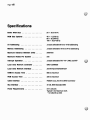
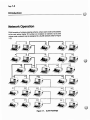
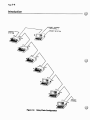
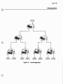


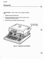

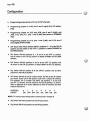
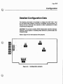

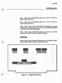


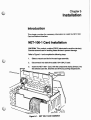

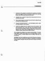


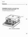


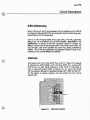
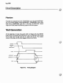
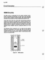
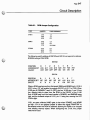


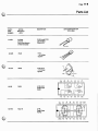


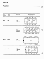
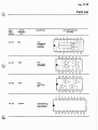
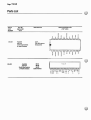
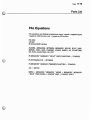


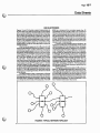
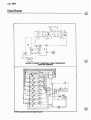

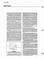

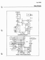
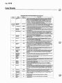
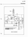


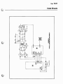

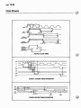


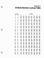

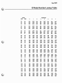


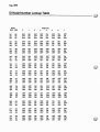
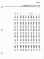


![ft.757gx ]i hf all mode computer aided transceiver](http://vs1.manualzilla.com/store/data/005735092_1-f8362b9c1e3279439f07a335507c2c8e-150x150.png)