1
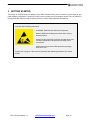
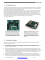
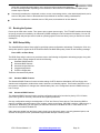
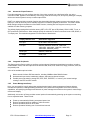
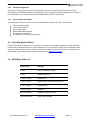
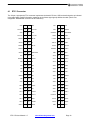
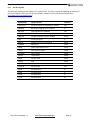
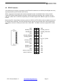
ETX-N270
ETX 3.0 Computer-On-Module Based on Intel® Atom N270
Revision
Date
Comment
1.1-1.4
10/27/10
Minor updates
1.5
3/24/11
Update for new version of COMs
FOR TECHNICAL SUPPORT
PLEASE CONTACT:
[email protected]
Copyright 2011
Diamond Systems Corporation
555 Ellis Street
Mountain View, CA 94043 USA
Tel 1-650-810-2500
Fax 1-650-810-2525
www.diamondsystems.com
CONTENTS
IMPORTANT SAFE-HANDLING INFORMATION ......................................................................................................3
1. INTRODUCTION .................................................................................................................................................4
1.1 Features .........................................................................................................................................................4
2. FUNCTIONAL OVERVIEW .................................................................................................................................6
2.1 Block Diagram ...............................................................................................................................................6
2.2 Board Dimensions, Mounting Holes, and Connectors...................................................................................7
2.3 Bus and Interface Connector Summary ........................................................................................................9
2.4 ETX Bus Connectors .....................................................................................................................................9
2.5 Other Interface Connectors ...........................................................................................................................9
3. GETTING STARTED........................................................................................................................................ 10
3.1 ETX Development Kits ............................................................................................................................... 11
3.2 Configuring the Hardware ........................................................................................................................... 11
3.3 Booting the System .................................................................................................................................... 12
3.4 BIOS Setup Utility ....................................................................................................................................... 12
3.4.1
Standard CMOS Features ................................................................................................................. 12
3.4.2
Advanced BIOS Features .................................................................................................................. 12
3.4.3
Advanced Chipset Features .............................................................................................................. 13
3.4.4
Integrated Peripherals ........................................................................................................................ 13
3.4.5
Power Management Setup ................................................................................................................ 13
3.4.6
PnP/PCI Configuration ....................................................................................................................... 14
3.4.7
Other Settings and Utilities ................................................................................................................ 14
3.5 Operating System Drivers .......................................................................................................................... 14
3.6 BIOS Beep Code List ................................................................................................................................. 14
4. INTERFACE CONNECTOR DETAILS ............................................................................................................. 15
4.1 ETX1 Connector ......................................................................................................................................... 16
4.1.1
PCI bus signals .................................................................................................................................. 17
4.1.2
USB signals ....................................................................................................................................... 18
4.1.3
Audio interface ................................................................................................................................... 18
4.1.4
Miscellaneous functions ..................................................................................................................... 19
4.2 ETX2 Connector ......................................................................................................................................... 20
4.3 ETX3 Connector ......................................................................................................................................... 21
4.3.1
Analog video output ........................................................................................................................... 22
4.3.2
TV video output .................................................................................................................................. 22
4.3.3
LCD interface ..................................................................................................................................... 23
4.3.4
Serial port interfaces .......................................................................................................................... 23
4.3.5
Keyboard, mouse, and infrared transceiver interfaces ...................................................................... 24
4.3.6
Parallel port interface ......................................................................................................................... 24
4.3.7
Floppy drive interface ......................................................................................................................... 25
4.3.8
Miscellaneous functions ..................................................................................................................... 26
4.4 ETX4 Connector ......................................................................................................................................... 27
4.4.1
IDE interfaces .................................................................................................................................... 28
4.4.2
Ethernet port ...................................................................................................................................... 29
4.4.3
Power control and management ........................................................................................................ 29
4.4.4
Miscellaneous signals ........................................................................................................................ 30
4.5 SATA Connectors ....................................................................................................................................... 30
4.6 SDVO Connector ........................................................................................................................................ 31
5. APPENDIX: SYSTEM RESOURCES REFERENCE ....................................................................................... 32
5.1 BIOS Memory Mapping .............................................................................................................................. 32
5.2 I/O Port Address Map ................................................................................................................................. 33
5.3 Interrupt Request (IRQ) Lines .................................................................................................................... 35
5.4 BIOS POST Codes ..................................................................................................................................... 36
ETX-270 User Manual 1.5
www.diamondsystems.com
Page 2
IMPORTANT SAFE-HANDLING INFORMATION
WARNING: ESD-Sensitive Electronic Equipment!
Observe ESD-safe handling procedures when working with this product.
Always use this product in a properly grounded work area and wear
appropriate ESD-preventive clothing and/or accessories.
Always store this product in ESD-protective packaging when not in use.
Safe Handling Precautions
The ETX-N270 contains numerous I/O connectors that connect to sensitive electronic components. This creates
many opportunities for accidental damage during handling, installation and connection to other equipment. The
list here describes common causes of failure found on boards returned to Diamond Systems for repair. This
information is provided as a source of advice to help you prevent damaging your Diamond (or any vendor’s)
embedded computer boards.
ESD damage – This type of damage is almost impossible to detect, because there is no visual sign of failure or
damage. The symptom is that the board simply stops working, because some component becomes defective.
Usually the failure can be identified and the chip can be replaced. To prevent ESD damage, always follow proper
ESD-prevention practices when handling computer boards.
Damage during handling or storage – On some boards we have noticed physical damage from mishandling. A
common observation is that a screwdriver slipped while installing the board, causing a gouge in the PCB surface
and cutting signal traces or damaging components.
Another common observation is damaged board corners, indicating the board was dropped. This may or may not
cause damage to the circuitry, depending on what is near the corner. Most of our boards are designed with at
least 25 mils clearance between the board edge and any component pad, and ground / power planes are at least
20 mils from the edge to avoid possible shorting from this type of damage. However these design rules are not
sufficient to prevent damage in all situations.
A third cause of failure is when a metal screwdriver tip slips, or a screw drops onto the board while it is powered
on, causing a short between a power pin and a signal pin on a component. This can cause overvoltage / power
supply problems described below. To avoid this type of failure, only perform assembly operations when the
system is powered off.
Sometimes boards are stored in racks with slots that grip the edge of the board. This is a common practice for
board manufacturers. However our boards are generally very dense, and if the board has components very close
to the board edge, they can be damaged or even knocked off the board when the board tilts back in the rack.
Diamond recommends that all our boards be stored only in individual ESD-safe packaging. If multiple boards are
stored together, they should be contained in bins with dividers between boards. Do not pile boards on top of each
other or cram too many boards into a small location. This can cause damage to connector pins or fragile
components.
Power supply wired backwards – Our power supplies and boards are not designed to withstand a reverse
power supply connection. This will destroy each IC that is connected to the power supply. In this case the board
will most likely will be unrepairable and must be replaced. A chip destroyed by reverse power or by excessive
power will often have a visible hole on the top or show some deformation on the top surface due to vaporization
inside the package. Check twice before applying power!
ETX-270 User Manual 1.5
www.diamondsystems.com
Page 3
1. INTRODUCTION
The ETX-N270 is a highly integrated computer-on-module (COM) based on the low power, high performance Intel
Atom N270 processor clocked at 1.6GHz. The module provides an SO-DIMM socket for up to 2GB of DDR2
DRAM, and provides interface controllers for high-resolution CRT and LVDS-interfaced displays, 10/100Mbps
Ethernet, SATA and IDE storage devices, USB 2.0, audio, serial, parallel, and PS/2 ports. Additionally, the ETXN270 provides a high degree of system expansion flexibility via the presence of both 32-bit PCI and 16-bit ISA
expansion buses on its ETX 3.0 compliant baseboard interface connectors.
1.1
Features
Processor:
Intel® Atom N270
533MHz FSB and 512KB L2 Cache
Chipset:
Intel 945GSE and Intel ICH7M
RAM:
200-pin SO-DIMM socket
Supports up to 2GB DDR2 SDRAM (400/533MHz)
Graphics:
Based on Intel GMA950 graphics core
VGA CRT interface; up to 2048x1536 resolution
Dual channel 18-bit LVDS flat panel interface (LVDS); provides LCD backlight control signals
TV output
Intel-compliant SDVO port supports VGA, DVI, LVDS, TV-out; up to 200 megapixels/sec data rate
(connector directly on ETX module)
Supports dual independent displays
Audio:
Realtek ALC655 AC’97 CODEC
Mic in, line in/out signals
IDE interface:
1 UltraATA 100/66/33 interface
Supports two devices (Master/Slave)
Usable in PIO or UDMA mode
SATA interfaces:
2 SATA ports, supporting one device each
Up to 150MB/s data transfer rates
Connectors directly on ETX COM module
Floppy/parallel port:
Shared interface
Parallel port supports SPP/EPP/ECP modes
Ethernet interface:
1 10/100Base-T port
Based on Realtek 8103EL
Serial ports:
2 16550-compatible ports
Logic-level signaling
Keyboard/mouse:
Standard PS/2 keyboard and mouse ports
USB keyboard/mouse also supported
ETX-270 User Manual 1.5
www.diamondsystems.com
Page 4
USB:
4 USB 2.0 ports
Other:
SMbus, IrDA serial interfaces
PC speaker interface
Watchdog timer; supports 255-level reset
Dual system expansion buses:
16-bit ISA bus
32-bit PCI bus; supports 4 PCI masters
Size:
ETX 3.0 compliant form-factor (physical and electrical)
4.5 x 3.7 inches (95mm x 114mm)
Input voltage:
System power: +5V DC +/-5%
Real-time clock backup: +2.0 to 3.6V DC
Operating environment:
o
o
o
o
-20 C to +71 C or -40 C to +85 C operating temperature
0 to 90% operating humidity (non-condensing)
BIOS:
Phoenix-Award PnP flash BIOS
Note: The ETX 3.0 specification is available for download from the ETX Industrial Group’s
website (http://www.etx-ig.de/specs/specs.php).
ETX-270 User Manual 1.5
www.diamondsystems.com
Page 5
2. FUNCTIONAL OVERVIEW
2.1
Block Diagram
Figure 1 shows the ETX-N270 COM’s functional blocks, ETX bus, and peripheral interface signals.
Figure 1: Functional Block Diagram
ETX-270 User Manual 1.5
www.diamondsystems.com
Page 6
2.2
Board Dimensions, Mounting Holes, and Connectors
The two diagrams below show the mechanical dimensions of the ETX-N270’s board outline and five mounting
holes, as well as the position of all connectors on both the top and bottom sides of the board.
Figure 2: Board Layout – Top
ETX-270 User Manual 1.5
www.diamondsystems.com
Page 7
Figure 3: Board Layout – Bottom
ETX-270 User Manual 1.5
www.diamondsystems.com
Page 8
2.3
Bus and Interface Connector Summary
The ETX-N270 has seven interface connectors, as listed in the tables below. With the exception of SDVO1, these
connectors are defined in accordance with the ETX 3.0 Computer-on-Module (COM) Specification. Signal
functions relating to all of the module’s interface connectors are discussed in greater detail in Section 4 of this
document.
2.4
2.5
ETX Bus Connectors
Connector
Location
Pins
Function
ETX1
Bottom
100
PCI bus, USB ports, audio interface, serial IRQ
ETX2
Bottom
100
ISA bus
ETX3
Bottom
100
VGA, LCD (LVDS), TV video, serial ports, PS2 keyboard
and mouse, parallel port, floppy interface
ETX4
Bottom
100
IDE ports, Ethernet, power supply control, speaker, RTC
2
(real-time clock) backup battery input, I C bus, SM bus
Other Interface Connectors
Connector
Location
Pins
Function
SATA1
Top
7
Serial ATA channel 1
SATA2
Top
7
Serial ATA channel 2
SDVO1
Bottom
30
Serial Digital Video Out (SDVO) port
ETX-270 User Manual 1.5
www.diamondsystems.com
Page 9
3. GETTING STARTED
This section of the ETX-N270 User Manual covers basic hardware setup, power connection, system boot-up, and
initial software configuration. First-time ETX-N270 users normally receive the product as part of one of Diamond’s
Development Kits, which provide everything needed to ensure rapid application development.
Important Safe-Handling Information
WARNING: ESD-Sensitive Electronic Equipment!
Observe ESD-safe handling procedures when working
with this product.
Always use this product in a properly grounded work area
and wear appropriate ESD-preventive clothing and/or
accessories.
Always store this product in ESD-protective packaging
when not in use.
Please refer to page 4 of this manual (“Important Safe-Handling Information”) for further
details.
ETX-270 User Manual 1.5
www.diamondsystems.com
Page 10
3.1
ETX Development Kits
To facilitate evaluation and development, the ETX-N270 is normally supplied pre-integrated into one of Diamond’s
ETX development kits (pictured below). This approach increases project efficiency and reduces risks by providing
a known good environment for rapid application development.
Diamond’s ETX development kits feature baseboards with I/O connectors for quick and easy access to nearly all
system interfaces, a CompactFlash socket, and modular PC/104-Plus expansion. The kits – which include both
generic models and application-oriented ETX baseboards in various form-factors – extend the ETX-N270’s
functionality by adding serial and LAN ports, RS-232/422/485 signal buffering, CompactFlash sockets, industryleading data acquisition I/O functions, and more. Additionally, the kits come with SO-DIMM memory, an extensive
set of interface cables, drivers for Linux and Windows operation, and full documentation.
Two examples appear below.
ETX form-factor development kit: Matches
the footprint of the ETX-N270 and provides
connectors for system I/O, CompactFlash,
PC/104-Plus expansion, two additional serial
ports, RS-232/422/485 buffering, a digital I/O
port, and a second Ethernet LAN interface.
3.2
EPIC form-factor development kit: Provides
connectors for system I/O, CompactFlash,
PC/104-Plus expansion, four additional serial
ports, RS-232/422/485 buffering, a second
Ethernet port, a 5V/7-28V DC-to-DC power
supply, and an industry-leading data acquisition
subsystem.
Configuring the Hardware
Assuming you are using one of Diamond’s baseboards and heat-spreaders or heatsinks with the ETX-N270,
prepare the hardware as follows:
If the SO-DIMM memory module is not already installed, carefully insert it into the socket provided on the topside of the ETX-N270 module. Refer to the specifications in the introduction of this manual for memory
capacity and speed requirements.
Secure the heat-spreader (or heatsink) to the top-side of the ETX-N270 module using the single short screw
provided with the heat-spreader (or heatsink), taking care to align the four corner mounting holes of the heatspreader (or heatsink) with the four corresponding standoffs on the top of the ETX-N270. Note: This mounting
screw attaches to the heat-spreader (or heatsink) via a hole near the middle of ETX-N270 module, and
screws in from the bottom-side of the ETX module.
Using the four long screws provided with the heat-spreader (or heatsink), secure the heat-spreader (or
heatsink) to the corresponding standoffs located in the four corners of the top of the ETX-N270 module. If the
ETX module is to being installed in an enclosure, align the heat-spreader’s (or heatsink’s) corner mounting
ETX-270 User Manual 1.5
www.diamondsystems.com
Page 11
holes with corresponding hole-pattern on the enclosure before inserting and tightening
the four mounting screws. Depending on the thickness of the enclosure or chassis material, slightly longer
screws may be required.
Connect the baseboard to a keyboard, monitor, mouse, mass storage device, other desired peripherals, and a
source of DC power. Refer to the baseboard’s User Manual for interface cabling considerations.
Connect the baseboard to a suitable source of DC power, as described in its User Manual.
3.3
Booting the System
Power-up the VGA video monitor. Then power-up the system power supply. The ETX-N270 module should begin
its boot-up sequence immediately, as evidenced by BIOS messages on the connected VGA display. You can run
the BIOS Setup utility and proceed to install an operating system on the boot drive just as you would on a normal
desktop PC.
3.4
BIOS Setup Utility
The Award BIOS provides a Setup utility for specifying system configuration and settings. Pressing the <Del> key
shortly after power is applied to the ETX-N270 launches the BIOS Setup utility. Watch for the following message:
Press <DEL> to Enter Setup
The BIOS Setup utility’s main menu provides access to the following configuration and settings pages, along with
several exit options. Setup categories include the following:
Standard CMOS features
Advanced BIOS features
Advanced chipset features
Integrated peripherals
PnP/PCI configuration
These are discussed briefly below.
3.4.1
Standard CMOS Features
The Standard CMOS Features function includes settings for RTC date/time initialization, IDE and floppy drive
detection and configuration, default video mode, and boot error handling options. This function should be re-run if
the system’s configuration is changed, the onboard battery fails, or the configuration stored in CMOS memory is
lost or corrupt.
3.4.2
Advanced BIOS Features
The Advanced BIOS Features function provides configuration options for boot device priority, CPU L3 Cache,
quick POST (power-on self test), and several other system parameters.
One key configuration setting is the designation of “First” and “Second” boot devices. This directs the BIOS to
scan for a bootable operating system in two locations, which can be floppy, CD-ROM, hard drive, USB devices, or
LAN devices. Additionally, you can specify an alternative location for the BIOS to scan, in case these are not
found or do not contain a bootable OS.
Other settings available from this Setup page include boot-up NumLock status, a security password option, and
selection of the system’s APIC (Advanced Programmable Interrupt Controller) mode.
ETX-270 User Manual 1.5
www.diamondsystems.com
Page 12
3.4.3
Advanced Chipset Features
From this setup page you can configure the size of the video controller’s on-chip frame buffer, set up the
controller’s DVMT (Dynamic Video Memory Technology) mode and memory size, and specify what type of display
will be used as the system’s boot-up console output device.
DVMT is an advanced video controller function that dynamically allocates system memory to be used as video
memory in order to efficiently use of available resources to maximize graphics performance. The DVMT-related
BIOS settings configure the behavior of the DVMT function, including how much system memory is made
available for video memory purposes.
The default display setting allows selection among CRT, LCD, CRT plus LCD (default), SDVO LVDS, TV out, or
CRT plus SDVO LVDS devices. Other settings specify the resolution of devices connected to the LCD, SDVO, or
TV output ports. The resolutions supported in each mode are listed below.
3.4.4
Display Interface Port
Resolutions Supported
CRT port
Up to 2048 x 1536 resolution
LCD port
640x480, 800x600, 1024x768, 1280x1024,
1400x1050, 1600x1200, 1280x768, 1680x1050,
1920x1200, 1204x678 (24-bit)
SDVO port
800x600, 1024x768,
TV output
NTSC, PAL
Integrated Peripherals
This Setup section offers the ability to configure various onboard functions and peripheral controllers, including
enable/disable, mode, and other options for the board’s USB, audio, IDE, Serial ATA, floppy controller, serial, IR,
and parallel ports.
A few of the available options include:
Mode controls for faster IDE data transfer, including 33MB/sec Ultra DMA33 feature
Onboard serial port mode, handshake, address, and interrupt channel selection
Parallel port mode selection among SPP, EPP, ECP, ECP+EPP, or “normal”, plus several settings
relating to the EPP and ECP modes
3.4.5
Power Management Setup
Here, you can specify a host of options that regulate how the board’s power management features behave.
Included are options for enabling/disabling the board’s ACPI (Advanced Configuration and Power Interface)
capabilities, and specifying the degree and behavior of power management relative to the system’s mass storage
devices and display.
Additionally, this section of Setup provides several options for automatically powering up the system or resuming
from a suspended state. These include:
Power-up automatically following unexpected power loss
Resume operation based on modem or LAN connection
Resume operation based on RTC alarm
Resume operation following one of several time intervals
ETX-270 User Manual 1.5
www.diamondsystems.com
Page 13
3.4.6
PnP/PCI Configuration
This section of Setup provides options for configuration of devices connected to the ETX-N270’s PCI bus,
including the choice between automatic “plug-and-play” (PnP) configuration of IRQ and DMA channel settings. If
PnP is disabled, you can specific desired IRQ and DMA channels for PCI devices here.
3.4.7
Other Settings and Utilities
A few additional status and control functions are available from Setup’s main menu. These include:
CPU temperature status
CPU cooling fan status
CPU voltage status
Reload default BIOS settings
Set system boot password
Exit Setup with or without saving changes
3.5
Operating System Drivers
Drivers for Windows XP and Linux 2.6, if required, are included on the Software and Documentation CD that is
provided along with the ETX-N270 or in its Development Kit. To locate the ETX-N270 module’s software drivers
on the CD, view the index.html file in the CD’s root directory, locate “Computer-on-Modules,” and then click on
“ETX-COMs.” This software is also available for download from Diamond’s website.
3.6
BIOS Beep Code List
Beep Sound
Message
1 short
System is booting normally
2 short
CMOS setting error
1 long + 1 short
DRAM error
1 long + 2 short
Display card or monitor connected error
1 long + 3 short
Keyboard error
1 long + 9 short
ROM error
long (continuous)
DRAM not inserted correctly
short (continuous)
Power supply problem
ETX-270 User Manual 1.5
www.diamondsystems.com
Page 14
4. INTERFACE CONNECTOR DETAILS
This section describes the functions available on all of the ETX-N270’s bus and I/O interface connectors. The
ETX 3.0 specification, which provides more detail regarding the signals present on the ETX1, ETX2, ETX3, and
ETX4 connectors, is available from the ETX Industrial Group’s website (http://www.etx-ig.de/specs/specs.php).
Also available from that site is the latest ETX Design Guide, which provides further details on the ETX connector
signal functions and interface considerations. Several other relevant specifications are referenced below.
ETX-270 User Manual 1.5
www.diamondsystems.com
Page 15
4.1
ETX1 Connector
The 100-pin, high-density ETX1 connector implements the board’s PCI bus, USB, and audio signals, as indicated
in the table below. Further information regarding each of these signal groups follows the table. (Note: Pins
designated “RESERVED” should be left unconnected.)
GND
1
2
GND
VCC
51
52
VCC
PCICLK3
3
4
PCICLK4
PAR
53
54
SERR#
GND
5
6
GND
GPERR#
55
56
RESERVED
PCICLK1
7
8
PCICLK2
PME#
57
58
USB2-
REQ3#
9
10
GNT3#
LOCK#
59
60
DEVSEL#
GNT2#
11
12
3V
TRDY#
61
62
USB3-
REQ2#
13
14
GNT1#
IRDY#
63
64
STOP#
REQ1#
15
16
3V
FRAME#
65
66
USB2+
GNT0#
17
18
RESERVED
GND
67
68
GND
VCC
19
20
VCC
AD16
69
70
CBE2#
SERIRQ
21
22
REQ0#
AD17
71
72
USB3+
AD0
23
24
3V
AD19
73
74
AD18
AD1
25
26
AD2
AD20
75
76
USB0-
AD4
27
28
AD3
AD22
77
78
AD21
AD6
29
30
AD5
AD23
79
80
USB1-
CBE0#
31
32
AD7
AD24
81
82
CBE3#
AD8
33
34
AD9
VCC
83
84
VCC
GND
35
36
GND
AD25
85
86
AD26
AD10
37
38
AUXAL
AD28
87
88
USB0+
AD11
39
40
MIC
AD27
89
90
AD29
AD12
41
42
AUXAR
AD30
91
92
USB1+
AD13
43
44
ASVCC
PCIRST#
93
94
AD31
AD14
45
46
SNDL
INTC#
95
96
INTD#
AD15
47
48
ASGND
INTA#
97
98
INTB#
CBE1#
49
50
SNDR
GND
99
100
GND
ETX-270 User Manual 1.5
www.diamondsystems.com
Page 16
4.1.1
PCI bus signals
This set of pins implements the module’s PCI expansion bus. For further information regarding the functions of
the PCI bus signals, refer to the PCI Bus Specification, available from the PCI Special Interest Group
(http://www.pcisig.com/specifications).
Signal Name
Signal function
Direction
PCICLK1-4
PCI clock outputs for external PCI devices
Out
REQ0-3#
Bus Request signals of PCI Masters
In
GNT0-3#
Grant signals to PCI Masters
Out
AD0-31
PCI address and data bus signals
In/Out
CBE0-3#
PCI Bus command and byte enables
In/Out
PAR
PCI bus parity bit
In
SERR#
System Error or PCI Clock RUN
In/Out
GPERR#
Parity Error
In/Out
PME#
Power management event
In/Out
LOCK#
Lock resource signal
In/Out
DEVSEL#
Device select
In/Out
TRDY#
Target ready
In/Out
IRDY#
Initiator ready
In/Out
STOP#
Stop
In/Out
FRAME#
Cycle frame
In/Out
PCIRST#
PCI bus reset
Out
INTA#
PCI interrupt A
In
INTB#
PCI interrupt B
In
INTC#
PCI interrupt C
In
INTD#
PCI interrupt D
In
ETX-270 User Manual 1.5
www.diamondsystems.com
Page 17
4.1.2
USB signals
These pins provide connections to the board’s four USB channels. For further information regarding the functions
of the USB signals listed above, refer to the USB 2.0 Specification, available from the USB Implementers Forum
(http://www.usb.org).
4.1.3
Signal Name
Signal Function
Direction
USB0+
USB Port 0 data +
In/Out
USB0-
USB Port 0 data -
In/Out
USB1+
USB Port 1 data +
In/Out
USB1-
USB Port 1 data -
In/Out
USB2+
USB Port 2 data +
In/Out
USB2-
USB Port 2 data -
In/Out
USB3+
USB Port 3 data +
In/Out
USB3-
USB Port 3 data -
In/Out
Audio interface
These pins carry stereo audio input and output as indicated.
Signal Name
Signal Function
Direction
SNDL
Line-level stereo output left; drives a 5k ohm load
Out
SNDR
Line-level stereo output right; drives a 5k ohm load
Out
AUXAL
Auxiliary A input left
In
AUXAR
Auxiliary A input right
In
MIC
Microphone input
In
ASGND
Analog ground
n/a
ASVCC
Power supply for audio controller
n/a
ETX-270 User Manual 1.5
www.diamondsystems.com
Page 18
4.1.4
Miscellaneous functions
These pins carry power and ground signals and an interrupt request as indicated.
Signal Name
Signal Function
Direction
VCC
+5V ±5% DC power input
In
GND
Power ground
n/a
3V
+3.3V ± 5% supply generated on the ETX module, for
powering external devices (500mA max. external load)
Out
RESERVED
Do not connect
n/a
SERIRQ
Serial interrupt request
In
Caution: Do not connect the 3V pins (pins 12 and 16) of EXT1 to an external power source!
ETX-270 User Manual 1.5
www.diamondsystems.com
Page 19
4.2
ETX2 Connector
The 100-pin, high-density ETX2 connector implements the board’s ISA bus signals, as indicated in the table
below. For further information on the module’s ISA bus signals, refer to the ETX 3.0 Specification.
GND
1
2
GND
VCC
51
52
VCC
SD14
3
4
SD15
SA6
53
54
IRQ5
SD13
5
6
MASTER#
SA7
55
56
IRQ6
SD12
7
8
DREQ7
SA8
57
58
IRQ7
SD11
9
10
DACK7#
SA9
59
60
SYSCLK
SD10
11
12
DREQ6
SA10
61
62
REFSH#
SD9
13
14
DACK6#
SA11
63
64
DREQ1
SD8
15
16
DREQ5
SA12
65
66
DACK1#
MEMW#
17
18
DACK5#
GND
67
68
GND
MEMR#
19
20
DREQ0
SA13
69
70
DREQ3
LA17
21
22
DACK0#
SA14
71
72
DACK3#
LA18
23
24
IRQ14
SA15
73
74
IOR#
LA19
25
26
IRQ13
SA16
75
76
IOW#
LA20
27
28
IRQ12
SA18
77
78
SA17
LA21
29
30
IRQ11
SA19
79
80
SMEMR#
LA22
31
32
IRQ10
IOCHRDY
81
82
AEN
LA23
33
34
IO16#
VCC
83
84
VCC
GND
35
36
GND
SD0
85
86
SMEMW
SBHE#
37
38
M16#
SD2
87
88
SD1
SA0
39
40
OSC
SD3
89
90
NOWS#
SA1
41
42
BALE
DREQ2
91
92
SD4
SA2
43
44
TC
SD5
93
94
IRQ9
SA3
45
46
DACK2#
SD6
95
96
SD7
SA4
47
48
IRQ3
IOCHK#
97
98
RSTDRV
SA5
49
50
IRQ4
GND
99
100
GND
ETX-270 User Manual 1.5
www.diamondsystems.com
Page 20
4.3
ETX3 Connector
The 100-pin ETX3 connector implements VGA, LCD (LVDS), TV-video, serial, parallel, floppy, mouse, and
keyboard signals. Because pins 51-100 are shared between floppy and parallel port functions, dual signal
assignments are indicated in the illustration below. Further information regarding each of these signal groups
follows. (Note: Pins designated “RESERVED” should be left unconnected.)
.
GND
1
2
GND
LPT/FLP#
51
52
RESERVED
R
3
4
B
VCC
53
54
GND
HSY
5
6
G
STB#/RESERVED
55
56
AFD#/DENSEL
VSY
7
8
DDCK
RESERVED
57
58
PD7/RESERVED
DETECT#
9
10
DDDA
IRRX
59
60
ERR#/HDSEL#
LCDDO16
11
12
LCDDO18
IRTX
61
62
PD6/RESERVED
LCDDO17
13
14
LCDDO19
RXD2
63
64
INIT#/DIR#
GND
15
16
GND
GND
65
66
GND
LCDDO13
17
18
LCDDO15
RTS2#
67
68
PD5/RESERVED
LCDDO12
19
20
LCDDO14
DTR2#
69
70
SLIN#/STEP#
GND
21
22
GND
DCD2#
71
72
PD4/DSKCHG#
LCDDO8
23
24
LCDDO11
DSR2#
73
74
PD3/RDATA#
LCDDO9
25
26
LCDDO10
CTS2#
75
76
PD2/WP#
GND
27
28
GND
TXD2
77
78
PD1/TRK0#
LCDDO4
29
30
LCDDO7
RI2#
79
80
PD0/INDEX#
LCDDO5
31
32
LCDDO6
VCC
81
82
VCC
GND
33
34
GND
RXD1
83
84
ACK#/DRV
LCDDO1
35
36
LCDDO3
RTS1#
85
86
BUSY/MOT
LCDDO0
37
38
LCDDO2
DTR1#
87
88
PE/WDATA#
VCC
39
40
VCC
DCD1#
89
90
SLCT/WGATE#
JILI_DAT
41
42
LTGIO0
DSR1#
91
92
MSCLK
JILI_CLK
43
44
BLON#
CTS1#
93
94
MSDAT
BIASON
45
46
DIGON
TXD1
95
96
KBCLK
COMP
47
48
Y
RI1#
97
98
KBDAT
SYNC
49
50
C
GND
99
100
GND
ETX-270 User Manual 1.5
www.diamondsystems.com
Page 21
4.3.1
Analog video output
These pins provide video, clock, and sync information for display on analog CRTs, or on LCD flat panels
that are compatible with analog CRT timings, as indicated.
4.3.2
Signal Name
Signal Function
Direction
HSY
Horizontal sync
Out
VSY
Vertical sync
Out
R
Red video output
Out
G
Green video output
Out
B
Blue video output
Out
DDCK
Display Data Channel Clock for DDC interface between
the board’s graphics controller and a monitor
In/Out
DDDA
Display Data Channel Data for DDC interface between
the board’s graphics controller and a monitor
In/Out
TV video output
These pins carry video and timing data for graphical display on a TV device, as indicated.
Signal Name
Signal Function
Direction
SYNC
Composite Sync for SCART PAL TVs with EURO AV compatible
connectors; alternately usable for video-related I/O
In/Out
Y
Luminance for S-Video; alternately Red for RGB video
Out
C
Chrominance for S-Video; alternately Green for RGB video
Out
COMP
Composite Video; alternately Blue for RGB video
Out
ETX-270 User Manual 1.5
www.diamondsystems.com
Page 22
4.3.3
LCD interface
These pins carry data for graphical display on an LCD panel, as indicated.
4.3.4
Signal Name
Signal Function
Direction
BIASON
Controls display contrast voltage
Out
DIGON
Controls digital power to LCD
Out
BLON#
Controls backlight power to LCD
Out
LCD0-LCD19
LVDS channel data 0-19
Out
DETECT#
Panel hot-plug detection
In
FPDDC_CLK DDC
DDC signals for flat panel detection and control
Out
FPDDC_DAT DDC
DDC signals for flat panel detection and control
In/Out
Serial port interfaces
These pins carry data and control information to/from the board’s two serial ports, as indicated. These pins
provide logic-level signaling, and require external I/O buffering if RS-232, RS-422, or RS-485 signaling is desired.
Signal Name
Signal Function
Direction
DTR1#, DTR2#
Data terminal ready outputs from serial ports 1 and 2
Out
RI1#, RI2#
Ring indicator inputs for serial ports 1 and 2
In
TXD1, TXD2
Transmit data outputs from serial ports 1 and 2
Out
RXD1, RXD2
Receive data inputs for serial ports 1 and 2
In
CTS1#, CTS2#
Clear to send signal inputs for serial ports 1 and 2
In
RTS1#, RTS2#
Request to send outputs from serial ports 1 and 2
Out
DCD1#, DCD2#
Data carrier detected inputs for serial ports 1 and 2
In
DSR1#, DSR2#
Data set ready inputs for serial ports 1 and 2
In
ETX-270 User Manual 1.5
www.diamondsystems.com
Page 23
4.3.5
Keyboard, mouse, and infrared transceiver interfaces
These pins carry data and clock signals associated with the board’s PS2 keyboard and mouse ports. Additionally,
transmit and receive data to/from an IR device, can be routed as indicated.
4.3.6
Signal Name
Signal Function
Direction
KBDAT
Data to/from keyboard.
In/Out
KBCLK
Clock signal to keyboard
Out
MSDAT
Data to/from mouse
In/Out
MSCLK
Clock signal to mouse.
Out
IRTX
Infrared transmit data
Out
IRRX
Infrared receive data
In
Parallel port interface
These pins carry data and control information to/from the board’s bidirectional parallel port, as indicated.
Signal Name
Signal Function
Direction
LPT/FLPY#
Interface configuration input
In
STB#
Printer data strobe
Out
AFD#
Automatic line feed request
Out
PD0-7
Bidirectional parallel data bus
In/Out
ERR#
Printer error
In
INIT#
Printer initialization control
Out
SLIN#
Printer select control
Out
ACK#
Printer ready to receive data
In
BUSY
Printer busy
In
PE
Printer out of paper
In
SLCT
Printer power on
In
Note: These pins are shared with the board’s floppy drive controller function, under control of the
LPT/FLPY# input signal. When that signal is left unconnected or held high, the port is placed in
parallel-port mode.
ETX-270 User Manual 1.5
www.diamondsystems.com
Page 24
4.3.7
Floppy drive interface
These pins carry data and control information to/from the board’s floppy drive controller, as indicated.
Signal Name
Signal Function
Direction
LPT/FLPY#
Interface configuration input
In
RESERVED
Do not connect
n/a
DENSEL
Diskette data density select
Out
INDEX#
Index hole indicator
In
TRK0#
Track 0 indicator
In
WP#
Write-protect indicator
In
RDATA#
Read data from drive
In
DSKCHG#
Drive door opened indicator
In
HDSEL#
Head select 0/1 control
Out
DIR#
Step head step direction control
Out
STEP#
Step pulse control
Out
DRV
Drive select control
Out
MOT#
Drive motor activation control
Out
WDATA#
Write data to drive
Out
WGATE#
Write enable control
Out
Note: These pins are shared with the board’s bidirectional parallel port function, under control of
the LPT/FLPY# input signal. When that signal is left unconnected or held high, the port is placed
in parallel-port mode.
ETX-270 User Manual 1.5
www.diamondsystems.com
Page 25
4.3.8
Miscellaneous functions
These pins carry power and ground signals and a GPIO signal, as indicated.
Signal Name
Signal Function
Direction
VCC
+5V ±5% DC power input
In
GND
Power ground
In/Out
RESERVED
Do not connect
n/a
LTGIO0
General purpose I/O
In/Out
ETX-270 User Manual 1.5
www.diamondsystems.com
Page 26
4.4
ETX4 Connector
The 100-pin ETX4 connector implements the board’s IDE, Ethernet, and a number of other signals, as indicated
in the table below. Further information regarding each of these signal groups follows the table.
GND
1
2
GND
SIDE_IOW#
51
52
PIDE_IOR#
5V_SB
3
4
PWGIN
SIDE_DRQ
53
54
PIDE_IOW#
PS_ON#
5
6
SPEAKER
SIDE_D15
55
56
PIDE_DRQ
PWRBTN#
7
8
BATT
SIDE_D0
57
58
PIDE_D15
KBINH#
9
10
LILED#
SIDE_D14
59
60
PIDE_D0
RSMRST#
11
12
ACTLED#
SIDE_D1
61
62
PIDE_D14
ROMKBCS#
13
14
SPEEDLED#
SIDE_D13
63
64
PIDE_D1
EXT_PRG
15
16
I2CLK
GND
65
66
GND
VCC
17
18
VCC
SIDE_D2
67
68
PIDE_D13
OVCR#
19
20
GPCS#
SIDE_D12
69
70
PIDE_D2
EXTSMI#
21
22
I2DAT
SIDE_D3
71
72
PIDE_D12
SMBCLK
23
24
SMBDATA
SIDE_D11
73
74
PIDE_D3
SIDE_CS3#
25
26
SMBALRT#
SIDE_D4
75
76
PIDE_D11
SIDE_CS1#
27
28
DASP_S
SIDE_D10
77
78
PIDE_D4
SIDE_A2
29
30
PIDE_CS3#
SIDE_D5
79
80
PIDE_D10
SIDE_A0
31
32
PIDE_CS1#
VCC
81
82
VCC
GND
33
34
GND
SIDE_D9
83
84
PIDE_D5
PDIAG_S
35
36
PIDE_A2
SIDE_D6
85
86
PIDE_D9
SIDE_A1
37
38
PIDE_A0
SIDE_D8
87
88
PIDE_D6
SIDE_INTRQ
39
40
PIDE_A1
GPE2#
89
90
CBLID_P#
BATLOW#
41
42
GPE1#
RXD#
91
92
PIDE_D8
SIDE_AK#
43
44
PIDE_INTRQ
RXD
93
94
SIDE_D7
SIDE_RDY
45
46
PIDE_AK#
TXD#
95
96
PIDE_D7
SIDE_IOR#
47
48
PIDE_RDY
TXD
97
98
HDRST#
VCC
49
50
VCC
GND
99
100
GND
ETX-270 User Manual 1.5
www.diamondsystems.com
Page 27
4.4.1
IDE interfaces
These pins carry data and control information to/from the board’s IDE drive controller, as indicated.
Signal Name
Signal Function
Direction
PIDE_D0-15
Primary IDE ATA bidirectional data bus
In/Out
PIDE_A0-2
Primary IDE ATA address bus
Out
PIDE_CS1#
Primary IDE chip select 1
Out
PIDE_CS3#
Primary IDE chip select 3
Out
PIDE_DRQ
Primary IDE DMA Request for IDE Master
In
PIDED_AK#
Primary IDE DACK# for IDE Master
Out
PIDE_RDY
Primary IDE Ready
In
PIDE_IOR#
Primary IDE IOR# command; function differs in Ultra-33 mode
Out
PIDE_IOW#
Primary IDE IOW# command; function differs in Ultra-33 mode
Out
PIDE_INTRQ
Primary channel interrupt request
In/Out
SIDE_D0-15
Secondary IDE ATA bidirectional data bus
In/Out
SIDE_A0-2
Secondary IDE ATA address bus
Out
SIDE_CS1#
Secondary IDE chip select 1
Out
SIDE_CS3#
Secondary IDE chip select 3
Out
SIDE_DRQ
Secondary IDE DMA Request for IDE Master
In
SIDED_AK#
Secondary IDE DACK# for IDE Master
Out
SIDE_RDY
Secondary IDE Ready
In
SIDE_IOR#
Secondary IDE IOR# command; function differs in Ultra-33 mode
Out
SIDE_IOW#
Secondary IDE IOW# command; function differs in Ultra-33 mode
Out
SIDE_INTRQ
Secondary channel interrupt request
In
DASP_S
Drive active or slave present on Secondary IDE channel
Out
PDIAG_S
Slave diagnostic passed indicator; function differs in DMA66 or DMA100
modes
In
HDRST#
Drive hardware reset
Out
CBLID_P#
Detects 80-conductor IDE cable on primary IDE channel
In
ETX-270 User Manual 1.5
www.diamondsystems.com
Page 28
4.4.2
Ethernet port
The ETX-N270’s 10/100Mbps Ethernet LAN interface signals on connector ETX4 require the use of an external
1:1 transformer. The ETX 3.0 specification provides further details regarding the transformer’s requirements.
4.4.3
Signal Name
Signal Function
Direction
TXD#, TXD
Transmit data differential pair
Out
RXD#, RXD
Receive data differential pair
In
ACTLED#
Out
LILED#
Data transmit/receive activity LED (on = data activity
present)
Link Integrity LED (on = link valid)
SPEEDLED#
Speed LED (on = 100Mbps, off = 10Mbps)
Out
Out
Power control and management
These pins support various power management and control functions, in conjunction with the board’s ACPI BIOS
functionality and system management embedded controller.
Signal Name
Signal Function
Direction
PWGIN
Power good input (power supply is ready)
In
5V_SB
+5V +/- 5% DC power input for suspend mode
In
PS_ON#
Signals power supply to remove all power except 5V_SB
Out
PWRBTN#
Power Button signal; supports ACPI Power Button function
In
RSMRST#
Resume Reset; resets internal power management logic
In
SMBALRT#
System Management Bus Alert from SM bus devices
In
BATLOW#
Battery low signal
In
GPE1#, GPE2#
General purpose power management event inputs
In
EXTSMI#
System management interrupt
In
ETX-270 User Manual 1.5
www.diamondsystems.com
Page 29
4.4.4
Miscellaneous signals
These pins implement the ETX-N270’s SM Bus interface, PC-speaker output, and RTC/CMOS backup power
input.
4.5
Signal Name
Signal Function
Direction
SPEAKER
This logic-level signal can drive a piezoelectric speaker
(typically via a transistor)
O
BATT
2.4V to 3.3V DC backup power input for RTC and CMOS
RAM; typically connects to an external 3V lithium cell
I
I2CLK
No connection
I/O
I2DAT
No connection
I/O
SMBCLK
Bidirectional SM Bus clock signal
I/O
SMBDATA
Bidirectional SM Bus data signal
I/O
KBINH#
Keyboard inhibit signal
In
OVCR#
USB over-current detected
In
ROMKBCS#
Reserved; do not connect
n/a
EXT_PRG
Reserved; do not connect
n/a
GPCS#
Reserved; do not connect
n/a
SATA Connectors
The ETX-N270 provides two SATA (Serial ATA) drive interfaces on a pair of 7-pin connectors located on the top
side of the board. The position and pinout of each of these connectors is compliant with the ETX 3.0 Specification.
The signal assignment appears below.
ETX-270 User Manual 1.5
1
GND
2
TX+
3
TX-
4
GND
5
RX+
6
RX-
7
GND
www.diamondsystems.com
Page 30
4.6
SDVO Connector
A low-profile 30-pin connector on the bottom of the ETX-N270 contains the set of SDVO (Serial Digital Video Out)
signals generated by the ETX-N270’s IHC7-M chip.
SDVO, a high-speed serial digital video interface developed by Intel, is a standard feature of many of Intel’s
newest PCI Express-enabled graphics controllers. SDVO uses differential signaling, and is capable of driving
CRT, DVI, LVDS, and TV-out devices. Specifically, the ETX-N270 supports the “SDVO B” signal set, as defined
by Intel.
Because the ETX 3.0 specification makes no provision for SDVO, the ETX-N270 provides an additional connector
for optional SDVO interfacing. The board’s SDVO interface supports maximum data rates of 200 megapixels/sec.
The interface connector is Hirose part number FH-12-30S-0.5SH. The SDVO connector’s signal pinout is shown
below.
ETX-270 User Manual 1.5
GND
1
16
GND
SDVOB_RED#
2
17
SDVOB_CTRLCLK
SDVOB_RED
3
18
SDVOB_CTRLDATA
GND
4
19
GND
SDVOB_GREEN#
5
20
NC
SDVOB_GREEN
6
21
NC
GND
7
22
BUF_PLT_RST#
SDVOB_BLUE#
8
23
+5V
SDVOB_BLUE
9
24
+5V
GND
10
25
+5V
SDVOB_CLKN
11
26
+5V
SDVOB_CLKP
12
27
GND
GND
13
28
GND
SDVO_FLDSTALL#
14
29
GND
SDVO_FLDSTALL
15
30
GND
www.diamondsystems.com
Page 31
5. APPENDIX: SYSTEM RESOURCES REFERENCE
5.1
BIOS Memory Mapping
Address
Device Description
E000:0000h - F000:FFFFh
System BIOS Area
D000:2000h - D000:FFFFh
Free space
D000:0000h - D000: FFFh
LAN ROM
C000:E000h - CF00:FFFFh
Free space
C000:0000h - C000:DFFFh
VGA BIOS
A000:0000h - B000:FFFFh
VGA RAM
0000:0000h - 9000:FFFFh
DOS 640K
ETX-270 User Manual 1.5
www.diamondsystems.com
Page 32
5.2
I/O Port Address Map
Each peripheral device in the system is assigned a set of I/O port addresses, which also become the identity of
the device. The following table lists the I/O port addresses used:
Address
Device Description
00000000 - 00000007
DMA Controller
00000000 - 00000CF7
PCI bus
00000010 - 0000001F
Motherboard Resource
00000020 - 00000021
Programmable Interrupt Controller
00000022 - 0000003F
Motherboard Resource
00000040 - 00000043
System Timer
00000044 - 0000005F
Motherboard Resource
00000060 - 00000060
Standard 0 / 02-Key or Microsoft Natural PS/2 Keyboard
00000061 – 00000061
System Speaker
00000062 - 00000063
Motherboard Resource
00000064 - 00000064
Standard 0 / 02-Key or Microsoft Natural PS/2 Keyboard
00000065 - 0000006F
Motherboard Resource
00000070 - 00000073
System CMOS/real time clock
00000074 - 0000007F
Motherboard Resource
00000080 - 00000090
DMA Controller
00000091 - 00000093
Motherboard Resource
00000094 - 0000009F
DMA Controller
000000A0 - 000000A1
Programmable Interrupt Controller
000000A2 - 000000BF
Motherboard Resource
000000C0 - 000000DF
DMA Controller
000000E0 - 000000EF
Motherboard Resource
000000F0 - 000000FF
Numeric Data Processor
000001F0 - 000001F7
Primary IDE Channel
00000274 - 00000277
ISAPNP Read Data Port
00000279 - 00000279
ISAPNP Read Data Port
00000294 - 00000297
Motherboard Resource
ETX-270 User Manual 1.5
www.diamondsystems.com
Page 33
000002E8 - 000002EF
Communications Port (COM4)
000002F8 - 000002FF
Communications Port (COM2)
00000378 - 0000037F
Printer Port (LPT )
000003B0 - 000003BB
Mobile Intel 94 Express Chipset Family
000003C0 - 000003DF
Mobile Intel 94 Express Chipset Family
000003E8 - 000003EF
Communications Port (COM3)
000003F6 - 000003F6
Primary IDE Channel
000003F8 - 000003FF
Communications Port (COM )
00000400 - 000004BF
Motherboard Resource
000004D0 - 000004D1
Motherboard Resource
00000500 - 0000051F
Intel 8280 G (ICH7 Family) SMBus Controller - 27DA
00000680 - 000006FF
Motherboard Resource
00000778 - 0000077B
Printer Port (LPT )
00000880 - 0000088F
Motherboard Resource
00000A78 - 00000A7B
Motherboard Resource
00000BBC - 00000BBF
Motherboard Resource
00000BBC - 00000BBF
Motherboard Resource
00000D00 - 0000FFFF
PCI bus
00000E78 - 00000E7B
Motherboard Resource
00000F78 - 00000F7B
Motherboard Resource
00000FBC - 00000FBF
Motherboard Resource
0000B000 - 0000BFFF
Intel 8280 G (ICH7 Family) PCI Express Root Port - 27D4
0000C000 - 0000CFFF
Intel 8280 G (ICH7 Family) PCI Express Root Port - 27D0
0000DF00 - 0000DF3F
Intel PRO/ 00 VE Network Connection
0000F000 - 0000F0FF
Realtek AC’97 Audio
0000F300 - 0000F30F
Intel 8280 GBM/GHM (ICH7-M Family) Serial ATA Storage Controller - 27C4
0000F400 - 0000F40F
Intel 8280 GBM/GHM (ICH7-M Family) Serial ATA Storage Controller - 27C4
0000F500 - 0000F50F
Intel 8280 GBM/GHM (ICH7-M Family) Serial ATA Storage Controller - 27C4
ETX-270 User Manual 1.5
www.diamondsystems.com
Page 34
5.3
Interrupt Request (IRQ) Lines
Peripheral devices use interrupt request lines to notify CPU when services are required. The table below lists the
interrupt request channels used by the ETX-N270’s onboard devices.
IRQ Level
Function
IRQ 01
Standard 0 / 02-Key or Microsoft Natural PS/2 Keyboard
IRQ 03
Communications Port
IRQ04
Communications Port
IRQ 08
System CMOS/real time clock
IRQ 09
Microsoft ACPI-Compliant System
IRQ 10
Communications Port
IRQ 11
Communications Port
IRQ 12
PS/2 Compatible Mouse
IRQ 13
Math Coprocessor
IRQ 14
Primary IDE Channel
IRQ 15
Intel 8280 G (ICH7 Family) SMBus Controller - 27DA
IRQ 16
Intel 8280 G (ICH7 Family PCI Express Root Port - 27D0
IRQ 16
Intel 8280 G (ICH7 Family) USB Universal Host Controller - 27CB
IRQ 16
Mobile Intel 94 GM Express Chipset Family
IRQ 17
Realtek AC’97 Audio
IRQ 18
Intel 8280 G (ICH7 Family) PCI Express Root Port - 27D4
IRQ 18
Intel 8280 G (ICH7 Family) USB Universal Host Controller - 27CA
IRQ 19
Intel 8280 G (ICH7 Family) USB Universal Host Controller - 27C9
IRQ 19
Intel 8280 G (ICH7-M Family) Serial ATA Storage Controller - 27C4
IRQ 19
Intel 8280 G (ICH7 Family) USB Universal Host Controller - 27C9
IRQ 20
Intel PRO/ 00 VE Network Connection
IRQ 23
Intel 8280 G (ICH7 Family) USB Universal Host Controller - 27C8
IRQ 23
Intel 8280 G (ICH7 Family) USB2 Enhanced Host Controller - 27CC
ETX-270 User Manual 1.5
www.diamondsystems.com
Page 35
5.4
BIOS POST Codes
The POST codes used by the ETX-N270’s on-board BIOS appear in the table below.
Code
Function
CFh
Test CMOS read/write functionality
C0h
Early chipset initialization: Disable shadow RAM, L2 cache (socket 7 and below), program
basic chipset registers
C1h
Detect memory: Auto detection of DRAM size, type and ECC, auto detection of L2 cache
(socket 7 and below)
C3h
Expand compressed BIOS code to DRAM
C5h
Call chipset hook to copy BIOS back to E000 & F000 shadow RAM
01h
Expand the Xgroup codes located in physical memory address 000:0
02h
Reserved
03h
Initial Super I/O_Early Init switch
04h
Reserved
05h
Blank out screen; Clear CMOS error flag
06h
Reserved
07h
Clear 8042 interface; Initialize 8042 self test
08h
Test special keyboard controller for Winbond 977 series Super I/O chips; enable keyboard
interface
09h
Reserved
0Ah
Disable PS/2 mouse interface (optional); auto-detect ports for keyboard and mouse
followed by a port and interface swap (optional); reset keyboard for Winbond 977 series
Super I/O chips
0Bh0Dh
Reserved
0Eh
Test F000h segment shadow to see whether it is read/write capable or not. If test fails,
keep beeping the speaker
0Fh
Reserved
10h
Auto detect flash type to load appropriate flash read/write codes into the run time area in
F000 for ESCD & DMI support
11h
Reserved
12h
Use “walking 1’s” algorithm to check out interface in CMOS circuitry. Also set real time
clock power status and then check for override
13h
Reserved
ETX-270 User Manual 1.5
www.diamondsystems.com
Page 36
14h
Program chipset default values into chipset. Chipset default values are MODBINable by
OEM customers
15h
Reserved
16h
Initial Early_Init_Onboard_Generator switch
17h
Reserved
18h
Detect CPU information including brand, SMI type (Cyrix or Intel) and CPU level ( 86 or
686)
191Ah
Reserved
1Bh
Initial interrupts vector table. If no special specified, all H/W interrupts are directed to
SPURIOUS_INT_HDLR & S/W interrupts to SPURIOUS_soft_HDLR
1Ch
Reserved
1Dh
Initial EARLY_PM_INIT switch
1Eh
Reserved
1Fh
Load keyboard matrix (notebook platform)
20h
Reserved
21h
HPM initialization (notebook platform)
22h
Reserved
23h
Check validity of RTC value; Load CMOS settings into BIOS stack. If CMOS checksum
fails, use default value instead; Prepare BIOS resource map for PCI & PnP use. If ESCD is
valid, take into consideration of the ESCD's legacy information; Onboard clock generator
initialization. Disable respective clock resource to empty PCI & DIMM slots; Early PCI
initialization - Enumerate PCI bus number, assign memory & I/O resource, search for a
valid VGA device & VGA BIOS, and put it into C000:0
2426h
Reserved
27h
Initialize INT 09 buffer
28h
Reserved
29h
Program CPU internal MTRR (P6 & PII) for 0-640K memory address; Initialize the APIC for
Pentium class CPU; Program early chipset according to CMOS setup; Measure CPU
speed; Invoke video BIOS
2A2Ch
Reserved
2Dh
Initialize multilanguage; put information on screen display, including Award title, CPU type,
CPU speed, etc.
2E32h
Reserved
33h
Reset keyboard except Winbond 977 series Super I/O chips
ETX-270 User Manual 1.5
www.diamondsystems.com
Page 37
343Bh
Reserved
3Ch
Test 82 4
3Dh
Reserved
3Eh
Test 82 9 interrupt mask bits for channel
3Fh
Reserved
40h
Test 92 9 interrupt mask bits for channel 2
4142h
Reserved
43h
Test 82 9 functionality
4446h
Reserved
47h
Initialize EISA slot
48h
Reserved
49h
Calculate total memory by testing the last double last word of each 64K page; Program
writes allocation for AMD K CPU
4A4Dh
Reserved
4Eh
Program MTRR of M CPU; initialize L2 cache for P6 class CPU and program cacheable
range; Initialize the APIC for P6 class CPU; On MP platform, adjust the cacheable range to
smaller one in case the cacheable ranges between each CPU are not identical
4Fh
Reserved
50h
Initialize USB
51h
Reserved
52h
Test all memory (clear all extended memory to 0)
5354h
Reserved
55h
Display number of processors (multi-processor platform)
56h
Reserved
57h
Display PnP logo; Early ISA PnP initialization and assign CSN to every ISA PnP device
58h
Reserved
59h
Initialize the combined Trend Anti-Virus code
5Ah
Reserved
5Bh
Show message for entering AWDFLASH.EXE from FDD (optional feature)
5Ch
Reserved
ETX-270 User Manual 1.5
www.diamondsystems.com
Page 38
5Dh
Initialize Init_Onboard_Super_IO switch; Initialize Init_Onboard_AUDIO switch
5E5Fh
Reserved
60h
Okay to enter Setup utility
6164h
Reserved
65h
Initialize PS/2 mouse
66h
Reserved
67h
Prepare memory size information for function call: INT h ax=E820h
68h
Reserved
69h
Turn on L2 cache
6Ah
Reserved
6Bh
Program chipset registers according to items described in Setup and Auto-Configuration
table
6Ch
Reserved
6Dh
Assign resources to all ISA PnP devices; Auto assign ports to onboard COM ports if the
corresponding item in Setup is set to “AUTO”
6Eh
Reserved
6Fh
Initialize floppy controller; Setup floppy related fields in 40:hardware
7072h
Reserved
73h
Enter AWDFLASH.EXE if: AWDFLASH.EXE is found in floppy dive and ALT+F2 is pressed
74h
Reserved
75h
Detect and install all IDE devices: HDD, LS 20, ZIP, CDROM...
76h
Reserved
77h
Detect serial ports and parallel ports
7879h
Reserved
7Ah
Detect and install coprocessor
7B7Eh
Reserved
7Fh
Switch back to text mode if full screen logo is supported: if errors occur, report errors & wait
for keys, if no errors occur or F1 key is pressed continue - Clear EPA or customization logo
8081h
Reserved
ETX-270 User Manual 1.5
www.diamondsystems.com
Page 39
82H
Call chipset power management hook: Recover the text fond used by EPA logo (not for full
screen logo), If password is set, ask for password
83H
Save all data in stack back to CMOS
84h
Initialize ISA PnP boot devices
85h
Final USB initialization; NET PC: Build SYSID structure; Switch screen back to text mode;
Set up ACPI table at top of memory; Invoke ISA adapter ROM’s; Assign IRQ’s to PCI
devices; Initialize APM; Clear noise of IRQ’s
8692h
Reserved
93h
Read HDD boot sector information for Trend Anti-Virus code
94h
Enable L2 cache; Program boot up speed; Chipset final initialization; Power management
final initialization; Clear screen and display summary table; Program K6 write allocation;
Program P6 class write combining
95h
Program daylight saving; update keyboard LED and typematic rate
96h
Build MP table; Build and update ESCD; Set CMOS century to 20h or 19h; Load CMOS
time into DOS timer tick; Build MSIRQ routing table
FFh
Boot attempt (INT 19h)
ETX-270 User Manual 1.5
www.diamondsystems.com
Page 40