1
Right choice for ultimate yield
LSIS strives to maximize customers' profit in gratitude of choosing us for your
partner.
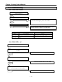
Programmable Logic Controller
XGB Analog
XGT Series
User’s Manual
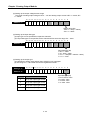
Voltage/Current input
XBF-AD04A
Voltage/Current output
XBF-DV04A
XBF-DC04A
Temperature input
XBF-RD04A
XBF-TC04S
Analog Combo
XBF-AH04A
Built-in PID
z Read
this manual carefully before
installing, wiring, operating, servicing
or inspecting this equipment.
z Keep
this manual within easy reach
for quick reference.
Safety Instructions
Before using the product …
For your safety and effective operation, please read the safety instructions
thoroughly before using the product.
► Safety Instructions should always be observed in order to prevent accident
or risk with the safe and proper use the product.
► Instructions are divided into “Warning” and “Caution”, and the meaning of
the terms is as follows.
Warning
This symbol indicates the possibility of serious injury
or death if some applicable instruction is violated
Caution
This symbol indicates the possibility of severe or
slight injury, and property damages if some
applicable instruction is violated
Moreover, even classified events under its caution category may develop into
serious accidents relying on situations. Therefore we strongly advise users to
observe all precautions properly just like warnings.
► The marks displayed on the product and in the user’s manual have the
following meanings.
Be careful! Danger may be expected.
Be careful! Electric shock may occur.
► The user’s manual even after read shall be kept available and accessible to
any user of the product.
Safety Instructions
Safety Instructions for design process
Warning
Please install a protection circuit on the exterior of PLC so that the
whole system may operate safely regardless of failures from
external power or PLC. Any abnormal output or operation from PLC
may cause serious problems to safety in whole system.
- Install protection units on the exterior of PLC like an interlock circuit
that deals with opposite operations such as emergency stop,
protection circuit, and forward/reverse rotation or install an interlock
circuit that deals with high/low limit under its position controls.
- If any system error (watch-dog timer error, module installation error,
etc.) is detected during CPU operation in PLC, all output signals are
designed to be turned off and stopped for safety. However, there
are cases when output signals remain active due to device failures
in Relay and TR which can’t be detected. Thus, you are
recommended to install an addition circuit to monitor the output
status for those critical outputs which may cause significant
problems.
Never overload more than rated current of output module nor
allow to have a short circuit. Over current for a long period time may
cause a fire .
Never let the external power of the output circuit to be on earlier
than PLC power, which may cause accidents from abnormal output or
operation.
Please install interlock circuits in the sequence program for safe
operations in the system when exchange data with PLC or modify
operation modes using a computer or other external equipments
Read specific instructions thoroughly when conducting control
operations with PLC.
Safety Instructions
Safety Instructions for design process
Caution
I/O signal or communication line shall be wired at least 100mm
away from a high-voltage cable or power line. Fail to follow this
instruction may cause malfunctions from noise
Safety Instructions on installation process
Caution
Use PLC only in the environment specified in PLC manual or
general standard of data sheet. If not, electric shock, fire, abnormal
operation of the product may be caused.
Before install or remove the module, be sure PLC power is off. If
not, electric shock or damage on the product may be caused.
Be sure that every module is securely attached after adding a
module or an extension connector. If the product is installed
loosely or incorrectly, abnormal operation, error or dropping may be
caused. In addition, contact failures under poor cable installation will
be causing malfunctions as well.
Be sure that screws get tighten securely under vibrating
environments. Fail to do so will put the product under direct
vibrations which will cause electric shock, fire and abnormal
operation.
Do not come in contact with conducting parts in each module,
which may cause electric shock, malfunctions or abnormal operation.
Safety Instructions
Safety Instructions for wiring process
Warning
Prior to wiring works, make sure that every power is turned off. If
not, electric shock or damage on the product may be caused.
After wiring process is done, make sure that terminal covers are
installed properly before its use. Fail to install the cover may cause
electric shocks.
Caution
Check rated voltages and terminal arrangements in each product
prior to its wiring process. Applying incorrect voltages other than
rated voltages and misarrangement among terminals may cause fire
or malfunctions.
Secure terminal screws tightly applying with specified torque. If
the screws get loose, short circuit, fire or abnormal operation may be
caused. Securing screws too tightly will cause damages to the module
or malfunctions, short circuit, and dropping.
*
Be sure to earth to the ground using Class 3 wires for FG
terminals which is exclusively used for PLC. If the terminals not
grounded correctly, abnormal operation or electric shock may be
caused.
Don’t let any foreign materials such as wiring waste inside the
module while wiring, which may cause fire, damage on the product
or abnormal operation.
Make sure that pressed terminals get tighten following the
specified torque. External connector type shall be pressed or
soldered using proper equipments.
Safety Instructions
Safety Instructions for test-operation and
maintenance
Warning
Don’t touch the terminal when powered. Electric shock or abnormal
operation may occur.
Prior to cleaning or tightening the terminal screws, let all the
external power off including PLC power. If not, electric shock or
abnormal operation may occur.
Don’t let the battery recharged, disassembled, heated, short or
soldered. Heat, explosion or ignition may cause injuries or fire.
Caution
Do not make modifications or disassemble each module. Fire,
electric shock or abnormal operation may occur.
Prior to installing or disassembling the module, let all the
external power off including PLC power. If not, electric shock or
abnormal operation may occur.
Keep any wireless equipment such as walkie-talkie or cell phones
at least 30cm away from PLC. If not, abnormal operation may be
caused.
When making a modification on programs or using run to modify
functions under PLC operations, read and comprehend all
contents in the manual fully. Mismanagement will cause damages to
products and accidents.
Avoid any physical impact to the battery and prevent
dropping as well. Damages to battery may cause leakage
fluid. When battery was dropped or exposed under strong
never reuse the battery again. Moreover skilled workers are
when exchanging batteries.
it from
from its
impact,
needed
Safety Instructions
Safety Instructions for waste disposal
Caution
Product or battery waste shall be processed as industrial waste.
The waste may discharge toxic materials or explode itself.
Revision History
Version
Data
Important change
V 1.0
2007. 7
1. Adding contents
(1) Setting Sequence before operation
(2) Accuracy calculation example
2. Changing contents
(1) Wiring examples
(2) Configuration and Function of Internal
Memory
(3) Example Program
V 1.1
2008. 1
Page
1. Adding model
(1) Thermocouple input module(XBF-TC04S)
2. Adding contents
(1) Thermo electromotive force and
compensating cable
(2) Performance Specification
(3) Dimension
3. Changing chapter number
(1) CH.6 PID Function
(2) Appendix 3. Dimension
V1.2
2008.4
1. Adding XGB compact ‘H’ type
V1.3
2009.7
1. Adding contents about XGB IEC type
2-1,3-1,4-1
2-9,3-7
2-13,3-9,4-9
2-28,3-18,4-20
2-34,3-23,4-24,5-37
Chapter 5
Appendix 2
1-5
APP.3-3
CH.5 --> CH.6
App.2 --> App.3
Chapter 1
Chapter 6
2. Adding model
(1) Analog combo module (XBF-AH04A)
3. Adding/changing contents
1-1,1-6,1-7
(1) Adding contents at chapter 1
Appendix3-3
(2) Adding dimension
※ The number of User’s manual is indicated right part of the back cover.
ⓒ LS Industrial Systems Co., Ltd
2007
All Rights Reserved.
About User’s Manual
About User’s Manual
Thank you for purchasing PLC of LS Industrial System Co., Ltd.
Before use, make sure to carefully read and understand the User’s Manual about the functions,
performances, installation and programming of the product you purchased in order for correct use and
importantly, let the end user and maintenance administrator to be provided with the User’s Manual.
The User’s Manual describes the product. If necessary, you may refer to the following description and order
accordingly. In addition, you may connect our website(http://eng.lsis.biz/) and download the information as a
PDF file.
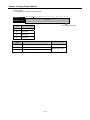
Relevant User’s Manuals
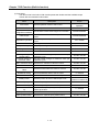
Title
XG5000 user’s
manual
Description
such as programming, printing, monitoring and debugging by
manual (for
such as programming, printing, monitoring and debugging by
Instructions &
Programming
XGI/XGR/XEC
Instructions &
Programming
XGB hardware
XGB hardware (IEC)
XGB Analog
user’s manual
XGB Position
User’s manual
10310000512
using XGB series products.
It describes how to use XG5000 software about online functions
XGK/XGK
Manual
It describes how to use XG5000 software about online functions
XG5000 user’s
XGI/XGR/XEC)
No. of User’s
10310000834
using XGB (IEC language)
It is the user’s manual for programming to explain how to use
10310000510
commands that are used PLC system with XGB CPU.
It is the user’s manual for programming to explain how to use
10310000833
commands that are used in XGB (IEC language)
It describes power, IO, extension specification and system
10310000693
configuration, built-in high speed counter of XGB main unit.
It describes power, IO, extension specification and system
10310000983
configuration, built-in high speed counter of XGB (IEC) main unit.
It describes how to use the specification of analog input/analog
output/temperature input module, system configuration and built-in
10310000920
PID control for XGB basic unit.
It describes how to use the specification of analog input/analog
output/temperature input module, system configuration and built-in
10310000927
PID control for XGB basic unit.
It is the user’s manual about XGB Cnet I/F that describes built-in
XGB Cnet I/F
communication function and external Cnet I/F module of XGB
10310000816
basic unit
XGB FEnet I/F
It describes how to use XGB FEnet I/F module.
10310000873
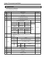
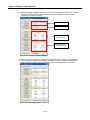
◎ Table of Contents ◎
Chapter 1 General ..................................................................................................1-1
1.1 Anlog Produt List.............................................................................................................................1-1
1.2 Specification of Anlog Module.........................................................................................................1-2
Chapter 2 Analog Input Module ...........................................................................2-1
2.1 Setting Sequence before Operation................................................................................................2-1
2.2 Specifications ................................................................................................................................2-2
2.3 Name of part and function .............................................................................................................2-4
2.4 Characteristic of I/O conversion ....................................................................................................2-5
2.5 Conversion Characteristic according to Input Range ....................................................................2-6
2.6 Accuracy ........................................................................................................................................2-9
2.7 Functions of Analog Input Module ...............................................................................................2-10
2.8 Wiring ..........................................................................................................................................2-13
2.9 Operation Parameter Setting ......................................................................................................2-17
2.10 Special Module Monitoring Functions .......................................................................................2-20
2.11 Register U devices ....................................................................................................................2-25
2.12 Configuration and Function of Internal Memory ........................................................................2-28
2.13 Example Program ......................................................................................................................2-34
2.14 Troubleshooting .........................................................................................................................2-40
Chapter 3 Analog Onput Module...........................................................................3-1
3.1 Setting Sequence before Operation ..............................................................................................3-1
3.2 Specification ..................................................................................................................................3-2
3.3 Designations and Functions ..........................................................................................................3-4
3.4 Characteristic of I/O Conversion ...................................................................................................3-5
3.5 Characteristic of Input/Output .......................................................................................................3-6
3.6 Accuracy ........................................................................................................................................3-7
3.7 Functions of Analog Output Module ..............................................................................................3-8
3.8 Wiring ............................................................................................................................................3-9
3.9 Operation Parameter Setting ......................................................................................................3-10
3.10 Special Module Monitoring Function .........................................................................................3-12
3.11 Register U devices ....................................................................................................................3-15
3.12 Internal memory ........................................................................................................................3-19
3.13 Example Program ......................................................................................................................3-24
3.14 Troubleshooting .........................................................................................................................3-27
Chapter 4 RTD Input Module .................................................................................4-1
4.1 Setting Sequence before Operation ..............................................................................................4-1
4.2 Specification ..................................................................................................................................4-2
4.3 Part Names and Functions ............................................................................................................4-4
4.4 Temperature Conversion Characteristic .......................................................................................4-5
4.5 Conversion Speed .........................................................................................................................4-6
4.6 Accuracy .........................................................................................................................................4-6
4.7 Temperature Display .....................................................................................................................4-6
4.8 Scaling Function ............................................................................................................................4-7
4.9 Disconnection Detection Function .................................................................................................4-8
4.10 Wiring ..........................................................................................................................................4-9
4.11 Filtering Function .......................................................................................................................4-11
4.12 Operation Parameter Setting ......................................................................................................4-12
4.13 Special Module Monitoring ........................................................................................................4-15
4.14 Register U devices ....................................................................................................................4-18
4.15 Configuration and Function of Internal Memory ........................................................................4-21
4.16 Example Program ......................................................................................................................4-25
4.17 Trouble Shooting .......................................................................................................................4-28
Chapter 5 Thermocouple Input Module................................................................5-1
5.1 General ...........................................................................................................................................5-1
5.2 Specification....................................................................................................................................5-3
5.3 Function ........................................................................................................................................5-11
5.4 Installation and Wiring...................................................................................................................5-16
5.5 Operation Setting and Monitor ....................................................................................................5-18
5.6 Configuration and Function of Internal Memory ..........................................................................5-32
5.7 Example Program ........................................................................................................................5-47
5.8 Troubleshooting ...........................................................................................................................5-52
Chapter 6 Analog Combo Module.........................................................................6-1
6.1 Pre-operation Setting Procedure ....................................................................................................6-1
6.2 Specification....................................................................................................................................6-2
6.3 Major Components..........................................................................................................................6-5
6.4 Conversion Characteristics by I/O Range.......................................................................................6-6
6.5 Precision .......................................................................................................................................6-10
6.6 Functions of Analog Combo Module.............................................................................................6-12
6.7 Wiring ............................................................................................................................................6-18
6.8 Operation Parameter Setting ......................................................................................................6-22
6.9 Special Module Monitor Function..................................................................................................6-24
6.10 Auto-registration of U-Device (Special Module Variable) ...........................................................6-28
6.11 Constitution and Function of Internal Memory ............................................................................6-33
6.12 Example Program .......................................................................................................................6-40
6.13 Troubleshooting ..........................................................................................................................6-46
Chapter 7 PID Function (Built-in function)...........................................................7-1
7.1 General ..........................................................................................................................................7-1
7.2 PID Control ....................................................................................................................................7-3
7.3 PID Instructions ..............................................................................................................................7-27
7.4 PID Auto-tuning ...........................................................................................................................7-33
7.5 Example Programs ......................................................................................................................7-42
7.6 Error/Warning Codes ...................................................................................................................7-54
Appendix …………………………………………………………………………
App.1-3
Appendix 1 Standard Resistor of Pt RTD .................................................................................... App.1-1
Appendix 2 Thermo Electromotive Force and Compensating Cable .......................................... App.2-1
Appendix 3 Dimension .................................................................................................................. App.3-1
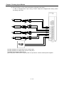
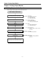
Chapter 1 General
Chapter 1 General
Here describes about analog module and built-in PID function of XGB series.
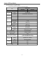
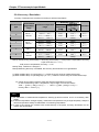
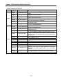
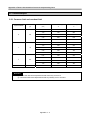
1.1 Analog Product List
Classification
Voltage/Current
input
Name
XBF-AD04A
No. of
channel
4
Range
Resolution
0 ~ 10V
2.5 ㎷
0 ~ 20㎃
4㎃ ~ 20㎃
Voltage output
XBF-DV04A
4
Current output
XBF-DC04A
4
XBF-RD04A
4
0 ~ 10V
0 ~ 20㎃
4㎃ ~ 20㎃
PT100
RTD input
XBF-RD01A
Thermocouple
XBF-
Input module
TC04S
1
JPT100
4
K/J/T/R
4~20mA
0~20mA
Analog combo
XBF-
2 (input)
(voltage/current I/O)
AH04A
2 (output)
1~5V
0~10V
1.Range selection by external switch and
parameter setting
2. External DC24V used
5.0 µA
2.5 ㎷
1. External DC24V used
2.Designates output in case of Error and CPU
5.0 µA
STOP
1. External DC24V used
0.1℃
Note1)
5.0 µA
1.25 ㎷
0~5V
Characteristic
2.5 ㎷
2. Filter function
1. External DC24V used
2. filter process, average process
1.Range selection by external switch and
parameter setting
2.Filter function, averaging function
3.Specifies output when error or CPU STOP
4. Uses external DC24V
Note1) for more detail, refer to Ch.5.2.6 accuracy/resolution.
Note2) To use analog combo module, the following version of basic unit is necessary
Basic unit
XGB S type
XGB H type
XGB IEC type
Version
V2.4
V1.7
V1.0
1-1
Chapter 1 General
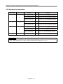
1.2 Specification of Analog Module
Here describes about specification of analog module of XGB series.
1.2.1 Analog input
Item
Analog input
range
XBF-AD04A
Type
Voltage
Current
Range
DC 0 ~ 10V
(Input resistance: 1 MΩ min.)
DC 4 ~ 20mA
DC 0 ~ 20mA
(Input resistance: 250 Ω)
Type
Digital output
12 bit binary data
Unsigned
value
0 ~ 4000
Signed value
-2000 ~ 2000
Range
Precise value
0 ~ 1000
Percentile
value
Max. resolution
400 ~ 2000/0 ~ 2000
0 ~ 1000
2.5㎷(1/4000)
5㎂(1/4000)
Accuracy
± 0.5% or less
Max. conversion speed
1.5ms/channel
Absolute max. input
DC ±15V
DC +25㎃
No. of output channel
4 channels
Insulation method
Photo-coupler insulation between input terminal and PLC power
(No insulation between channels)
Connection Terminal
11 point terminal block
I/O points occupied
Fixed type: 64 points
Max. number of equipment
7 (when using XBM-DxxxS “S”type)
10 (when using XB(E)C-DxxxH “H”type)
Consumption
current
Inner (DC 5V)
120mA
External (DC 24V)
62mA
Weight
64g
Additional function
Filter-processing, average-processing (time, count)
1-2
Chapter 1 General
1.2.2 Analog output
Item
XBF-DV04A
XBF-DC04A
Type
Voltage
Current
Range
DC 0 ~ 10V
(Load resistance: 2kΩ or more)
DC 4 ~ 20mA
DC 0 ~ 20mA
(Load resistance: 510Ω or less)
Analog output
Type
Digital input
12 bit binary data
Unsigned value
0 ~ 4000
0 ~ 4000
Signed value
-2000 ~ 2000
-2000 ~ 2000
Precise value
0 ~ 1000
400 ~ 2000/0 ~ 2000
Percentile
value
0 ~ 1000
0 ~ 1000
2.5㎷(1/4000)
5㎂(1/4000)
Range
Max. resolution
Accuracy
± 0.5% or less
Max. conversion speed
1㎳/channel
Absolute max. output
DC ±15V
DC +25㎃
No. of output channel
4 channels
Insulation method
Photo-coupler insulation between output terminal and PLC power
(no insulation between channel)
Connection Terminal
11 point terminal block
I/O points occupied
64 points
Max. number of equipment
7 (when using XBM-DxxxS “S”type)
10 (when using XB(E)C-DxxxH “H”type)
Consumption
current
Inner (DC 5V)
110mA
110mA
External (DC 24V)
70mA
120mA
64g
70g
Weight
Additional function
Designates output in case of error and CPU STOP
1-3
Chapter 1 General
1.2.3 RTD input
Item
XBF-RD04A
No. of input channel
4 channels
PT100
JIS C1604-1997
JPT100
JIS C1604-1981 , KS C1603-1991
PT100
-200 ~ 600℃
JPT100
-200 ~ 600℃
PT100
-2000 ~ 6000
JPT100
-2000 ~ 6000
Scaling display
0 ~ 4000
Normal temp. (25℃)
± 0.3% or less
Full temp. (0~55℃)
± 0.5% or less
Input sensor
type
Input temp.
range
Digital output
Accuracy
Conversion speed
Insulation
method
40ms / channel
Between channels
No insulation
terminal – PLC power
Insulation (Photo-Coupler)
Terminal block
15 point terminal
I/O points occupied
64 points
Max. number of equipment
7 (when using XBM-DxxxS “S”type)
10 (when using XB(E)C-DxxxH “H”type)
Sensor wiring method
3 line
Additional
function
Consumption
current
Filter function
Digital filter (160 ~ 64000ms)
Alarm function
Disconnection detection
Inner DC5V
100mA
External DC24V
100mA
Weight
63g
1-4
Chapter 1 General
1.2.4 Thermocouple input
Items
Specification
Number of input channel
4 channels
Thermocouple K / J / T / R type
Type of input sensor
JIS C1602-1995
K
-200.0℃ ~ 1300.0℃
Range of input
J
-200.0℃ ~ 1200.0℃
temperature
T
-200.0℃ ~ 400.0℃
R
0.0℃ ~ 1700.0℃
Displaying down to one decimal place – note1)
Temp. display
Digital output
K, J, T type: 0.1℃, R type: 0.5℃
Scaling display
Unsigned scaling (0 ~ 65535)
(user-defined scaling)
Signed scaling (-32768 ~ 32767)
Ambient temperature(25℃)
Within ± 0.2% – note 2)
Accuracy
Temp. coefficient
(range of operating temp)
Conversion velocity
Insulation
method
50ms / channel
Terminal – inner circuit
Photo-coupler insulation
Terminal – operating power
DC/DC converter insulation
Between channels
Photo-moss relay insulation
Insulation
400 V AC, 50/60 Hz, 1min,
Insulation pressure
leakage current 10㎃ or below
Insulation resistance
Standard contact
point
500 V DC, 10 MΩ or above
Auto compensation by RJC sensing (Thermistor)
±1.0℃
Compensation amount
compensation
± 100 ppm/℃
Warming-up time
20 min or above
Terminal block
11 point terminal
I/O occupied points
64 points
7 (when using XBM-DxxxS “S”type)
10 (when using XB(E)C-DxxxH “H”type)
Max. number of equipment
Digital filter (200 ~ 64,000㎳)
Filter process
Time average (400~64,000㎳)
Average process
Count average (2~64,000 times)
Additional function
Moving average (2~100)
Alarm
Disconnection detection
Max./Min. display
Display Max./Min.
Scaling function
Signed scaling / Unsigned scaling
Consumption
Inner DC5V
100㎃
current
External DC24V
100㎃
Weight
63g
Note1), Note2) For more detail specification, refer to 5.2.6 accuracy/resolution.
1-5
Chapter 1 General
1.2.5 Analog combo
(1) Input performance specification
Items
Input performance specifications
No. of input channel
Type
Analog
input
Range
range
2 channels
Voltage
Current
DC 1 ~ 5V
DC 4 ~ 20㎃
DC 0 ~ 5V
DC 0 ~ 20㎃
DC 0 ~ 10V
(input resistor 250 Ω)
(input resistor: 1 MΩ or above)
Input range can be set through external voltage/current selector switch after
setting at user program or I/O parameter per input channel
Type
Unsigned
value
Signed value
Digital
output
Range
Precise
value
Percentile
value
12bit binary data
0 ~ 4000
-2000 ~ 2000
100 ~ 500 (DC 1 ~ 5V)
400 ~ 2000 (DC 4 ~ 20㎃)
0 ~ 500 (DC 0 ~ 5V)
0 ~ 2000 (DC 0 ~ 20㎃)
0 ~ 1000 (DC 0 ~ 10V)
0 ~ 1000
1/4000
Max. resolution
1.25㎷ (DC 1~5V, 0~5V)
5㎂ (DC4~20㎃, 0~20㎃)
2.5㎷ (DC 0~10V)
Precision
±0.5% or less
Max. conversion speed
1ms/channel
Absolute max. input
Filter function
Additional
Averaging
function
function
Alarm function
DC ±25㎃
DC ±15V
Digital filter (4 ~ 64,000㎳)
Time averaging (4~16,000㎳)
Cyclic averaging (2~64,000cycle)
Moving averaging (2~100samples)
Disconnection detection (DC 1~5V, DC4~20㎃)
1-6
Chapter 1 General
(2) Output performance specification
Items
Output performance specification
No. of output channel
Type
Analog
output
Range
range
2 channels
Voltage
Current
DC 1 ~ 5V
DC 4 ~ 20㎃
DC 0 ~ 5V
DC 0 ~ 20㎃
DC 0 ~ 10V
(Load resistor 510 Ω or less)
(Load resistor: 2kΩ or above)
Input range can be set through external voltage/current selector switch after
setting at user program or I/O parameter per input channel
Type
Unsigned
value
Signed value
Digital
input
Range
Precise
value
Percentile
value
12 bit binary data
0 ~ 4000
-2000 ~ 2000
100 ~ 500 (DC 1 ~ 5V)
400 ~ 2000 (DC 4 ~ 20㎃)
0 ~ 500 (DC 0 ~ 5V)
0 ~ 2000 (DC 0 ~ 20㎃)
0 ~ 1000 (DC 0 ~ 10V)
0 ~ 1000
1/4000
Max. resolution
1.25㎷ (DC 1~5V, 0~5V)
5㎂ (DC4~20㎃, 0~20㎃)
2.5㎷ (DC 0~10V)
Precision
±0.5% or less
Max. conversion speed
1ms/channel
Absolute max. output
Additional function
DC 25㎃
DC ±15V
Function setting channel output status
(Can select one among Previous, Minimum, median, maximum)
(3) I/O common performance specification
Items
Insulation method
I/O terminal block
No. of I/O occupation point
Max. number of equipment
I/O common performance specification
Photo coupler insulation between I/O terminal and PLC power (not
insulated between channels)
11 points terminal block
Fixed type: 64 points
7 (when using XBM-DxxxS “S” type)
10 (when using XB(E)C-DxxxH “H” type)
Consumption
Internal (DC 5V)
120mA
current
External (DC 24V)
130mA
Weight
73g
1-7
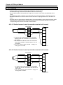
Chapter 2 Analog Input Module
Chapter 2 Analog Input Module
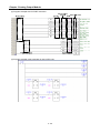
2.1 Setting Sequence before operation
Before using the analog input module, follow steps below.
XBF-AD04A
Checking performance specification
Specification (2.2 performance specification)
z Operating environment
z Input type and range
z Digital output range
Wiring
Wiring
z Wiring power (External DC24V)
z Wiring analog input
Setting external voltage/current switch
Setting switch
z Setting voltage/current input type
Reading analog input data
Analog input test
z XG5000 special module monitor test mode
Setting parameter
Parameter
z XG5000 I/O parameter
Programming
Programming
z Programming for reading analog data
(U device)
Refer to trouble shooting when there is error
or analog data is not normal.
2-1
Chapter 2 Analog Input Module
2.2 Specifications
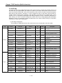
2.2.1 General specifications
General specifications are as follows.
No.
1
2
3
4
Items
Related
standards
Specification
Operating
temp.
Storage
temp.
Operating
humidity
Storage
humidity
0 ~ 55 °C
−25 ~ +70 °C
5∼95%RH (Non-condensing)
5∼95%RH (Non-condensing)
For discontinuous vibration
Frequency
10 ≤ f
5
Vibration
<
57Hz
57 ≤ f ≤
150Hz
-
Acceleration
Amplitude
−
0.075mm
9.8m/s2(1G)
−
For continuous vibration
Frequency
10 ≤ f
6
7
8
9
10
11
Shocks
Noise
Ambient
conditions
Operating
height
Pollution
degree
Cooling type
<
57Hz
Acceleration
Amplitude
−
0.035mm
Number
Each 10
times in
X,Y,Z
directions
57 ≤ f ≤
4.9m/s2(0.5G)
−
150Hz
• Max. impact acceleration : 147 m/s2(15G)
• Authorized time : 11ms
• Pulse wave : Sign half-wave pulse (Each 3 times in X,Y,Z
directions)
Square wave
±1,500 V
impulse noise
Electrostatic
Voltage : 4kV(contact discharging)
discharging
Radiated
electromagnetic
27 ~ 500 MHz, 10V/m
field noise
Digital/
Power
Fast
Analog I/O
Class
module
Transient
communication interface
/burst
noise
Voltage
2kV
1kV
No corrosive gas or dust
2000m or less
2 or less
Natural air cooling
2-2
IEC61131-2
IEC61131-2
LSIS standard
IEC61131-2
IEC61000-4-2
IEC61131-2,
IEC61000-4-3
IEC61131-2
IEC61000-4-4
Chapter 2 Analog Input Module
2.2.2 Performance specifications
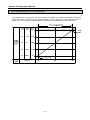
Performance specifications are as follows.
Items
Analog input
range
XBF-AD04A
Type
Voltage
Current
Range
DC 0 ~ 10V
(Input resistance: 1 MΩ min.)
DC 4 ~ 20mA
DC 0 ~ 20mA
(Input resistance 250 Ω)
Type
12 bit binary data
Signed value
0 ~ 4000
Unsigned
value
-2000 ~ 2000
Digital output
Range
Precise
value
0 ~ 1000
Percentile
value
Max. resolution
400 ~ 2000/0 ~ 2000
0 ~ 1000
2.5㎷(1/4000)
5㎂(1/4000)
Accuracy
±0.5% or less
Max. conversion speed
1.5ms/channel
Absolute max. output
DC ±15V
DC ±25㎃
No. of output channel
4 channels
Insulation method
Photo-coupler insulation between input terminal and PLC power
(No insulation between channels)
Connection terminal
11 point terminal block
I/O points occupied
Fixed type: 64 points
Consumption
current
Inner (DC 5V)
120mA
External (DC 24V)
62mA
Weight
64g
Additional function
Filter-processing, average-processing (time, count)
Notes
1) When A/D conversion module is released from the factory, Offset/Gain value is as adjusted for respective
analog input ranges, which is unavailable for user to change.
2) Offset Value: Analog input value where digital output value is 0 when digital output format is set to
Unsigned Value.
3) Gain Value: Analog input value where digital output value is 16000 when digital output format is set to
Unsigned Value.
2-3
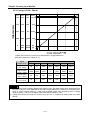
Chapter 2 Analog Input Module
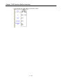
2.3 Name of part and function
Respective designations of the parts are as described below.
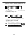
①
③
②
No.
Description
RUN LED
①
▪ Displays the operation status of XBF-AD04A
On: Operation normal
Flickering: Error occurs (page 12-30)
Off: Module error
Terminal block
②
▪ Analog input terminal, whose respective channels can be connected with
external devices.
Voltage/Current selection switch
③
▪ Switch for voltage and current selection of analog input
2-4
Chapter 2 Analog Input Module
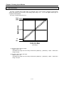
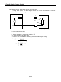
2.4 Characteristic of I/O conversion
Characteristics of I/O conversion are the inclination connected in a straight line between Offset and
Gain values when converting analog signal (voltage or current input) from PLC’s external device to
digital value. I/O conversion characteristics of A/D conversion modules are as described below.
2-5
Chapter 2 Analog Input Module
2.5 Conversion Characteristic according to Input Range
Voltage input range can be set through user program or special module package for respective
channels. Output formats of digital data are as specified below;
A. Unsigned Value
B. Signed Value
C. Precise Value
D. Percentile Value
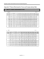
2.5.1 If the range is DC 0 ~ 10V
Digital output value for voltage input characteristic is as specified below.
(Resolution (based on 1/4000): 2.5 mV)
Digital output
range
Analog input voltage (V)
0
2.5
5
7.5
10
10.11
Unsigned value
(0 ~ 4047)
0
1000
2000
3000
4000
4047
Signed value
(-2000 ~ 2047)
-2000
-1000
0
1000
2000
2047
Precise value
(0 ~ 1011)
0
250
500
750
1000
1011
Percentile value
(0 ~ 1011)
0
250
500
750
1000
1011
▪
2-6
Chapter 2 Analog Input Module
2.5.2 If the range is DC 0 ~ 20mA ▪
▪ Digital output value for current input characteristic is as specified below.
(Resolution (based on 1/4000): 5 ㎂)
Digital output
range
Analog input current (㎃)
0
5
10
15
20
20.23
Unsigned value
(0 ~ 4047)
0
1000
2000
3000
4000
4047
Signed value
(-2000 ~ 2047)
-2000
-1000
0
1000
2000
2047
Precise value
(0 ~ 2023)
0
500
1000
1500
2000
2023
Percentile value
(0 ~ 1011)
0
250
500
750
1000
1011
2-7
Chapter 2 Analog Input Module
2.5.3 If range is DC4 ~ 20mA ▪
▪ Digital output value for current input characteristic is as specified below.
(Resolution (Based on 1/4000): 5 ㎂)
Digital
Output range
Analog input current (㎃)
0
4
8
12
16
20
20.23
Unsigned value
(-48 ~ 4047)
-48
0
1000
2000
3000
4000
4047
Signed value
(-2048 ~ 2047)
-2048
-2000
-1000
0
1000
2000
2047
Precise value
(381 ~ 2023)
381
400
800
1200
1600
2000
2023
Percentile value
(-12 ~ 1011)
-12
0
250
500
750
1000
1011
Notes
1) If analog input value exceeding digital output range is input, the digital output value will be kept to be
the max. or the min. value applicable to the output range specified. For example, if the digital output
range is set to unsigned value (0 ~ 4000) and the digital output value exceeding 4047 or analog
value exceeding –0 is input, the digital output value will be fixed as 0~4047.
2) Voltage and current input shall not exceed ±15 V and ±25 ㎃ respectively. Rising heat may cause
defects.
2-8
Chapter 2 Analog Input Module
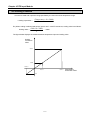
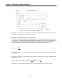
2.6 Accuracy
Accuracy of digital output value does not changed even if input range is changed. Figure below
shows the range of the accuracy with analog input range of 0 ~ 10 V and digital output type of
unsigned value selected.
Accuracy of XBF-AD04A is ±0.5%.
[ Accuracy ]
(1) Accuracy when using 5V input
4000 × 0.5% = 20
Therefore the range of the accuracy will become (2000-20) ~ (2000+20) = 1980 ~ 2020 when
using 5V input.
(2) Accuracy when using 10V input
4000 × 0.5% = 20
Therefore the range of the accuracy will become (4000-20) ~ (4000+20) = 3980 ~ 4020 when
using 10V input.
2-9
Chapter 2 Analog Input Module
2.7 Functions of Analog Input Module
Functions of XBF-AD04A conversion module are as described below.
Function
Description
Channel Run/Stop
setting
(1) Specify Run/Stop of the channel to execute A/D conversion.
(2) If the unused channel is set to Stop, whole Run time can be reduced.
Input voltage/Current
range setting
(1) Specify analog input range to be used.
(2) Select range in parameter setting after select Voltage/Current switch.
Output data format
setting
(1) Specify digital output type.
(2) 4 output data formats are provided in this module.
A/D conversion
methods
(1) Sampling processing
Sampling process will be performed if A/D conversion type is not specified.
(2) Filter processing
Used to delay the sudden change of input value.
(3) Average processing
Outputs average A/D conversion value based on frequency or time.
There are three A/D conversion methods, sampling processing, filter processing and average processing.
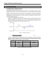
Sampling Processing
A/D Conversion Methods
Filter Processing
Average Processing
Time Average
Count Average
(1) Sampling processing
It collects analog input sign through general A/D conversion processing at a specific interval so to
convert to digital. The time required for A/D conversion of analog input sign till saved on the memory
depends on the number of channels used.
(Processing time) = (Number of channels used) X (Conversion speed)
(Ex.) If the number of channels used is 3, its process time will be
3 x 1.5 ㎳ = 4.5 ㎳
Sampling is to calculate the sampling value of continuous analog sign at a specific interval.
2 - 10
Chapter 2 Analog Input Module
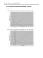
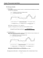
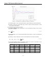
(2) Filter processing
Filter process function is used to obtain stable digital output value by filtering (delaying) noise or
sudden change of input value. Filter constant can be specified for respective channels through user
program or I/O parameters setting.
• Setting range: 1 ~ 99 (%)
F[n] = (1 - α) x A[n] + α x F [n - 1]
F[n]: Present filter output value
A[n]: Present A/D converted value
F[n-1]: Previous filter output value
Α: Filter constant (0.01 ~ 0.99: previous value added)
If filter setting value is not specified within 1 ~ 99, RUN LED blinks at an interval of 1 second. In
order to set RUN LED to On status, reset the filter setting value within 1 ~ 99 and then convert
PLC CPU from STOP to RUN. Be sure to use request flag of error clear (UXY.11.0) to clear the
error through modification during RUN.
• Analog input range: DC 0 ~ 10 V, Digital output range: 0 ~ 4000
• If analog input value changes 0 V → 10 V (0 → 4000), filter output value based on α value is
as specified below.
Filter output value
αvalue
α value
0 scan
1 scan
2 scan
3 scan
*1)
0.01
0
3600
3960
3997
1% inclined toward previous value
*2)
0.66
0
1360
2257
2850
50% inclined toward previous value
*3)
0.99
0
40
80
119
99% inclined toward previous value
*1) 4000 output after about 4 scans
*2) 4000 output after about 18 scans
*3) 4000 output after about 950 scans(1.19 s for 1 channel Run)
If filter process function is not used, present A/D converted value will be output as it is. The filter
process function takes value-added data between ‘Present A/D converted value’ and ‘Previous
A/D converted value’. And the value-added data can be decided with filter constant. If output
data shakes too much, set a big filter constant value.
(3) Average processing
This process is used to execute A/D conversion of the channel designated for specified frequency or
for specified time and save the average of the accumulated sum on memory. Average processing
option and time/frequency value can be defined through user program or I/O parameters setting for
respective channels.
(a) What is the average process used for
This process is used for A/D conversion of abnormal analog input signal such as noise to a value
near to normal analog input signal.
(b) Average processing type
Average processing type is of time average and count average.
1) Time average processing
▪ Setting range: 4 ~ 16000 (ms)
▪ Average processing count within specified time is decided based on the number of channels
used.
Average processing
count =
(Number
2 - 11
Setting time
of Channels used) x ( Conversion
Speed)
Chapter 2 Analog Input Module
Ex.1) Channels used: 1, setting time: 16000 ms
Average
processing
count
16000 ms
1 × 1 . 5 ms
=
=
10667 times
Ex.2) Channels used: 4, setting time: 4 ms
Average
processing
count
=
4 ms
4 × 1 . 5 ms
=
1 times
If setting value of time average is not specified within 4 ~ 16000, RUN LED blinks at an interval
of 1 second. In order to set RUN LED to On status, reset the setting value of time average within
4 ~ 16000 and then convert PLC CPU from STOP to RUN. Be sure to use request flag of error
clear (UXY.11.0) to clear the error through modification during RUN.
• Time average is processed after converted to average of the times inside the A/D conversion
module. In this case, a remainder may be produced when setting time is divided by (number of
channels used X conversion speed), which will be disregarded. Thus, the average processing
frequency will be the quotient of [(setting time) ÷ (number of channels used x conversion
speed)].
Ex.) If the number of channels used is 5, and setting time is 151 ms
151 ms ÷ (4 X 1.5 ms) = 26 times …… Remainder of 2 → 26 times
2) Count average process
• Setting range: 2 ~ 64000 (times)
• The time required for average value to be saved on memory when frequency average used
depends on the number of channels used.
Process time = setting frequency X number of channels used X conversion speed
If setting value of count average is not specified within 2 ~ 64000, RUN LED blinks at
an interval of 1 second. In order to set RUN LED to On status, reset the setting value
of frequency average within 2 ~ 64000 and then convert PLC CPU from STOP to
RUN. Be sure to use request flag of error clear (UXY.11.0) to clear the error through
modification during RUN.
Ex.) If the number of channels used is 4, and average processing frequency is 50
50 X 4 X (1.5 ms) = 300 ms
2 - 12
Chapter 2 Analog Input Module
2.8 Wiring
2.8.1 Precaution for wiring
(1) Don’t let AC power line near to A/D conversion module’s external input sign line. With an enough
distance kept away between, it will be free from surge or inductive noise.
(2) Cable shall be selected in due consideration of ambient temperature and allowable current,
whose size is not less than the max. cable standard of AWG22 (0.3㎟).
(3) Don’t let the cable too close to hot device and material or in direct contact with oil for long, which
will cause damage or abnormal operation due to short-circuit.
(4) Check the polarity when wiring the terminal.
(5) Wiring with high-voltage line or power line may produce inductive hindrance causing abnormal
operation or defect.
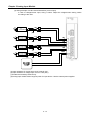
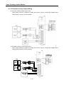
2.8.2 Wiring examples
(1) Example of voltage wiring
- In case of voltage/current input, wiring is same. Adjust the voltage/current setting switch
according to the case.
CH0
+
-
CH1
+
CH0+
-
CH0CH1+
CH1-
CH2
CH2+
+
CH2-
-
CH3+
CH3-
CH3
DC24V+
+
DC24V-
-
DC power
(For analog
supply)
(a) Input resistance of current input circuit is 250 Ω (typ.).
(b) Input resistance of voltage input circuit is 1 MΩ (min.).
(c) Enable the necessary channel only.
(d) Analog input module doesn’t support power for input device. Use the external power supplier.
2 - 13
Chapter 2 Analog Input Module
(2) Wiring example of 2-Wire sensor/transmitter (current input)
- In case of voltage/current input, wiring is same. Adjust the voltage/current setting switch
according to the case.
(a) Input resistance of current input circuit is 250 Ω (typ.).
(b) Input resistance of voltage input circuit is 1 MΩ (min.).
(c) Enable the necessary channel only.
(d) Analog input module doesn’t support power for input device. Use the external power supplier.
2 - 14
Chapter 2 Analog Input Module
(3) Wiring example of 4-Wire sensor/transmitter (Voltage/Current input)
- In case of voltage/current input, wiring is same. Adjust the voltage/current setting switch
according to the case.
(a) Input resistance of current input circuit is 250 Ω (typ.).
(b) Input resistance of voltage input circuit is 1 MΩ (min.).
(c) Enable the necessary channel only.
(d) Analog input module doesn’t support power for input device. Use the external power supplier.
2 - 15
Chapter 2 Analog Input Module
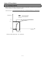
(4) Relationship between voltage input accuracy and wiring length
In voltage input, the wiring (cable) length between transmitter or sensor and module has an effect
on digital-converted values of the module as specified below;
Rs
Rc
Vs
Vin
Ri
Rc
Load
Analog input (Voltage)
Where,
Rc: Resistance value due to line resistance of cable
Rs: Internal resistance value of transmitter or sensor
Ri: Internal resistance value (1㏁) of voltage input module
Vin: Voltage allowed to analog input module
% Vi: Tolerance of converted value (%) due to source and cable length in voltage input
Vin =
Ri × Vs
[Rs + (2 × Rc ) + Ri ]
⎛ Vin ⎞
%Vi = ⎜1 −
⎟ × 100 %
Vs ⎠
⎝
2 - 16
Chapter 2 Analog Input Module
2.9 Operation Parameter Setting
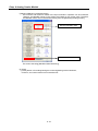
A/D conversion module’s operation parameters can be specified through XG5000’s [I/O parameters].
(1) Settings
For the user’s convenience of A/D conversion module, XG5000 provides GUI (Graphical User
Interface) for parameters setting of A/D conversion module. Setting items available through [I/O
parameters] on the XG5000 project window are as described below in the table.
Item
Details
[I/O parameter]
(1) Specify the following setting items necessary for the module
operation.
- Channel Enable/Disable setting
- Setting ranges of input voltage/current
- Output data format setting
- Filter processing Enable/Disable setting
- Filter constant setting
- Average processing Enable/Disable setting
- Average processing method setting
- Average value setting
(2) The data specified by user through S/W package will be saved on A/D
conversion module when [Special Module Parameters] are
downloaded. In other words, the point of time when [Special Module
Parameters] are saved on A/D conversion module has nothing to do
with PLC CPU’s status RUN or STOP.
(2) I/O Parameter setting
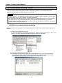
(a) Run XG5000 to create a project.
(Refer to XG5000 program manual for details on how to create the project)
(b) Double-click [I/O parameters] on the project window.
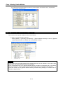
(c) On the ‘I/O parameters setting’ screen, find and click the slot of the base A/D conversion
module is installed on. 8-channel voltage type of A/D conversion module is installed on Base No.0,
Slot No.4 in this description.
2 - 17
Chapter 2 Analog Input Module
(d) Click the arrow button on the screen above to display the screen where an applicable module
can be selected. Search for the applicable module to select.
(e) After the module selected, click [Details].
(f) A screen will be displayed for you to specify parameters for respective channels as shown below.
Click a desired item to display parameters to set for respective items.
2 - 18
Chapter 2 Analog Input Module
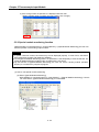
2.10 Special Module Monitoring Functions
Functions of Special Module Monitoring are as described below.
(1) Monitor/Test
Through applicable XG5000 menu of [Monitor] -> [Special Module Monitoring], A/D converted
value can be monitored and the operation of A/D conversion module can be tested.
(2) Monitoring the max./min. value
The max./min. value of the channel can be monitored during Run. However, the max./min. value
displayed here is based on the present value shown on the screen. Accordingly, when
[Monitoring/Test] screen is closed, the max./min. value will not be saved.
▪ The parameters specified for the test of A/D conversion module on the “Special Module
Monitoring” screen of [Special Module Monitoring] will be deleted the moment the “Special
Module Monitoring” screen is closed. In other words, the parameters of A/D conversion module
specified on the “Special Module Monitoring” screen will not be saved in [I/O parameters] located
Not saved in [I/O
parameters]
▪ Test function of [Special Module Monitoring] is provided for user to check the normal operation of
A/D conversion module even without sequence programming. If A/D conversion module is to be
used for other purposes than a test, use parameters setting function in [I/O parameters].
2 - 19
Chapter 2 Analog Input Module
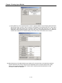
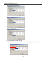
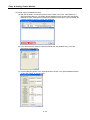
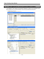
2.10.1 How to use special module monitoring
Monitoring special module will be based on XBF-AD04A.
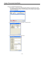
(1) Start of [Special Module Monitoring]
Go through [OnLine] -> [Connect] and [Monitor] -> [Special Module Monitoring] to start. If the
status is not [OnLine], [Special Module Monitoring] menu will not be active.
(2) How to use [Special Module Monitoring]
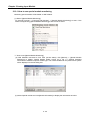
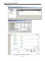
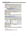
(a) With XG5000 connected to PLC CPU (on-line status), click [Monitor] -> [Special Module
Monitoring] to display ‘Special Module Select’ screen as in Fig. 5.1 showing base/slot
information in addition to special module type. The module installed on the present PLC system
will be displayed on the list dialog box.
(b) Select Special module and click [Module information] to display the information as below.
2 - 20
Chapter 2 Analog Input Module
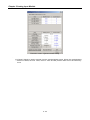
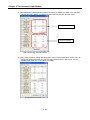
(c) Click [Monitor] on the “Special Module” screen in [Special Module List] to display [Special Module
Monitoring] screen as below, where 4 options are available such as [Reset max./min. value], [start
Monitoring], [Test] and [Close]. A/D conversion module’s output value and max./ min. value are
displayed on the monitoring screen at the top of the screen, and parameters items of respective
modules are displayed for individual setting on the test screen at the bottom of the screen.
(d) [Start Monitoring]: Click [Start Monitoring] to display A/D converted value of the presently operated
channel. Below screen is the monitoring screen displayed when the whole channels are in Stop
status. In the present value field at the screen bottom, presently specified parameters of A/D
conversion module are displayed
2 - 21
Chapter 2 Analog Input Module
.
Execution screen of [Start Monitoring]
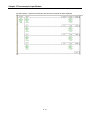
(e) [Test]: [Test] is used to change the presently specified parameters of A/D conversion module.
Click the setting value at the bottom field of the screen to change parameters. Below screen
will be displayed after [Test] is executed with channels 0’s input voltage range changed to 0~20 mA in the state of input not wired.
Execution screen of [Test]
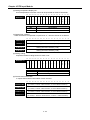
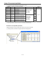
(f) [Reset max/min value]: The max/min value field at the upper screen shows the max. value and the
min. value of A/D converted value. Click [Reset max/min value] to initialize the max./min. value.
Below screen is after [Reset max/min value] button is clicked in the screen of Special Module
Monitor, where channel 0’s A/D converted value can be checked as reset.
2 - 22
Chapter 2 Analog Input Module
Execution screen of [Reset max/min value]
.
(g) [Close]: [Close] is used to escape from the monitoring/test screen. When the monitoring/test
screen is closed, the max. value, the min. value and the present value will not be saved any
more.
2 - 23
Chapter 2 Analog Input Module
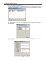
2.11 Register U devices
Register the variables for each module referring to the special module information that is set in the I/O
parameter. The user can modify the variables and comments.
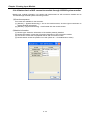
(1) Procedure
(a) Select the special module type in the [I/O Parameter Setting] window.
(b) Double click ‘Variable/Comment’ from the project window.
(c) Select [Edit] – [Register U Device].
2 - 24
Chapter 2 Analog Input Module
(d) Click ‘Yes’.
(e) As shown below, the variables are registered.
(f) For IEC type, as shown below, the variables are registered.
(2) Save variables
(a) The contents of ‘View Variable’ can be saved as a text file.
(b) Select [Edit] -> [Export to File].
(c) The contents of ‘View variable’ are saved as a text file.
2 - 25
Chapter 2 Analog Input Module
(3) View variables
The example of XGB ‘S’ type and ‘H’ type is as follows.
(a) The example program of XG5000 is as shown below.
(b) Select [View] -> [Variables]. The devices are changed into variables.
(c) Select [View] -> [Devices/Variables]. Devices and variables are both displayed.
2 - 26
Chapter 2 Analog Input Module
(d) Select [View] -> [Device/Comments]. Devices and comments are both displayed.
(e) In case of IEC, you can see variables with diverse option at ‘View’ menu like (b)~(d). The following
is example selecting ‘View Variable/Comment’ at IEC type.
2 - 27
Chapter 2 Analog Input Module
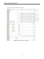
2.12 Configuration and Function of Internal Memory
A/D conversion module has the internal memory to transmit/receive data to/from PLC CPU.
2.12.1 I/O area of A/D converted data
I/O area of A/D converted data is as displayed in table.
Device assigned
(“S” or “H” type)
UXY.00.0
UXY.00.F
UXY.01.0
UXY.01.1
UXY.01.2
UXY.01.3
UXY.02
UXY.03
UXY.04
UXY.05
UXY.11.0
Device assigned
(IEC type)
%UX0.x.0
%UX0.x.15
%UX0.x.16
%UX0.x.17
%UX0.x.18
%UX0.x.19
%UW0.x.2
%UW0.x.3
%UW0.x.4
%UW0.x.5
%UX0.x.176
Details
Module ERROR flag
Module READY flag
CH0 Run flag
CH1 Run flag
CH2 Run flag
CH3 Run flag
Ch0 digital output value
Ch1 digital output value
Ch2 digital output value
Ch3 digital output value
Flag to request error clear
R/W
Sign direction
R
A/D → CPU
R
A/D → CPU
R
R
R
R
W
A/D → CPU
CPU → A/D
- In the device assigned, X stands for the Base No. and Y for the Slot No. on which module is installed.
- In order to read ‘CH1 digital output value’ of A/D conversion module installed on Base No.0, Slot No.4,
it shall be displayed as U04.03. (in case of IEC type, %UW0.4.3)
IEC type
“S” or “H” type
Base No
%UW0.4.3
Device Type
Word
Slot No.
- In order to read ‘Flag to detect CH4 disconnection’ of A/D conversion module installed on Base No.0,
Slot No.5, it shall be displayed as U05.10.4.
IEC type
“S” or “H” type
Base No
% U X 0 . 5 . 19
Device Type
Bit
Slot No.
2 - 28
Chapter 2 Analog Input Module
(1) Module Ready/Error flag (U0x.00, x: slot number)
(a) U0x.00.F: It will be ON when PLC CPU is powered or reset with A/D conversion ready to
process A/D conversion.
(b) U0x.00.0: It is a flag to display the error status of A/D conversion module.
Bit8
Bit7
Bit6
Bit5
Bit4
Bit3
Bit2
Bit1
—
—
—
—
—
—
—
—
—
—
—
—
—
—
Bit0
Error
(UW0.x.0)
Bit9
Ready
U0x.00
Bit15 Bit14 Bit13 Bit12 Bit11 Bit10
Error status
Bit On (1): error, Bit Off (0): normal
Module READY
Bit On (1): normal, Bit Off (0): error
(2) Run channel flag (UXY.01, X: Base No., Y: Slot No.)
The area where Run information of respective channels is saved
* XGB series base number is 0
UXY.01
B15 B14 B13 B12 B11 B10
B9
B8
B7
B6
B5
B4
B3
B2
B1
B0
—
—
—
—
—
—
—
C
H
3
C
H
2
C
H
1
C
H
0
—
—
—
—
—
(%UW0.x.1)
Run channel information
Bit ON (1): During Run, Bit Off (0): Operation Stop
(3) Digital output value (UXY.02 ~ UXY.09, X: Base No., Y: Slot No.)
(a) A/D converted-digital output value will be output to buffer memory addresses UXY.02 ~
UXY.05 (%UW0.x.2 ~ %UW0.x.5) for respective channels.
(b) Digital output value will be saved in 16-bit binary.
※ XGB PLC’s base number is 0.
B15 B14 B13 B12 B11 B10
U0x.02
U0x.03
U0x.04
U0x.05
B9
B8
B7
B6
B5
B4
B3
Channel 0 digital output value
Channel 1 digital output value
Channel 2 digital output value
Channel 3 digital output value
2 - 29
B2
B1
B0
(%UW0.x.2)
(%UW0.x.3)
(%UW0.x.4)
(%UW0.x.5)
Chapter 2 Analog Input Module
(4) Flag to request error clear (( ) means the case of IEC type, x: slot number)
(a) If a parameters setting error occurs, address No.22’s error code will not be automatically
erased even if parameters are changed correctly. At this time, turn the ‘error clear request’ bit
ON to delete address No.22’s error code and the error displayed in XG5000’s [System Monitor].
In addition, RUN LED which blinks will be back to On status.
(b) The ‘flag to request error clear’ shall be used surely together with UXY.00.0 attached thereon
for guaranteed Normal operation.
※ XGB PLC base number is 0
B15 B14 B13 B12 B11 B10 B9
B8
B7
B6
B5
B4
B3
B2
B1
B0
—
—
—
—
—
—
—
—
—
C
UXY.11.0
E
—
—
—
—
—
—
(%UX0.x.11)
R
Flag to request error clear (UXY.11.0)
Bit ON (1): Error clear request, Bit Off (0): Error clear standing-by
[How to use the flag to request error clear (“S” type or “H” type)]
[How to use the flag to request error clear (IEC type)]
2 - 30
Chapter 2 Analog Input Module
2.12.2 Operation parameters setting area
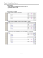
Setting area of A/D conversion module’s Run parameters is as described in Table.
Memory address
Hex.
Dec.
0H
0
1H
2H
3H
4H
5H
6H
7H
CH
DH
EH
FH
10H
11H
16H
Details
R/W
Remark
Channel enable/disable setting
R/W
Setting ranges of input
1
R/W
voltage/current
2
Output data format setting
R/W
Filter processing enable/disable
3
R/W
setting
4
CH0 filter constant
5
CH1 filter constant
R/W
6
CH2 filter constant
7
CH3 filter constant
Average processing enable/disable
12
R/W
setting
13
Average processing method setting
R/W
14
CH0 average value
15
CH1 average value
R/W
16
CH2 average value
17
CH3 average value
22
Error code
R/W
※R/W is to denote Read/Write if available from PLC program.
PUT
PUT
PUT
PUT
PUT
PUT
GET
(1) Setting operation channels
If the channel to use is not specified, all the channels will be set to Prohibited.
bit15 bit14 bit13 bit12 bit11 bit10
bit9
bit8
bit7
bit6
bit5
bit4
—
—
—
—
—
—
bit3
bit2
bit1
bit0
Address 0
— —
—
—
—
—
CH. CH. CH. CH.
3
2
1
0
Setting channel to use (bit)
Bit On (1): Run, Bit Off (0): Stop
(2) Setting input range
The range of analog voltage input is DC 0~10V, the range of analog current input is DC 4~20mA.
bit15 bit14 bit13 bit12 bit11 bit10
bit9
bit8
—
—
bit7
bit6
bit5
bit4
bit3
bit2
bit1
bit0
Address 1
— —
—
—
—
—
CH.3
CH.2
CH.1
Setting input range (bit)
Æ 00: 0 ~ 10V(4 ~ 20mA)
Æ 01: 0 ~ 20mA
Æ 11: 4 ~ 20mA
2 - 31
CH.0
Chapter 2 Analog Input Module
(3) Setting output data type
(a) The range of digital output data for analog input can be specified for respective channels.
(b) If the output data range is not specified, the range of all the channels will be set to 0 ~ 4000.
bit15 bit14 bit13 bit12 bit11 bit10
bit9
bit8
—
—
bit7
bit6
bit5
bit4
bit3
bit2
bit1
bit0
Address 2
— —
—
—
—
—
CH.3
CH.2
CH.1
CH.0
Setting output data type (bit)
Æ 00: 0 ~ 4000
Æ 01: -2000 ~ 2000
Æ 10: 0 ~ 1000(400 ~ 2000/0 ~ 2000)
Æ 11: 0 ~ 1000
(4) Setting filter process
If the filter process is not specified, the filter process of all channels will not be executed.
bit15 bit14 bit13 bit12 bit11 bit10
bit9
bit8
bit7
bit6
bit5
bit4
—
—
—
—
—
—
bit3
bit2
bit1
bit0
Address 3
— —
—
—
—
—
CH. CH. CH. CH.
3
2
1
0
Setting filter process (bit)
Bit On (1): used, bit Off (0): not used
(5) Setting filter constant
When using the filter process, specify the filter constant.
bit15 bit14 bit13 bit12 bit11 bit10
bit9
bit8
bit7
bit6
bit5
Address 5
CH.0 filter constant
CH.1 filter constant
Address 6
CH.2 filter constant
Address 7
CH.3 filter constant
Address 4
bit4
bit3
bit2
bit1
bit0
(6) Setting average process
If the average process is not specified, the average process of all channels will not be executed.
bit15 bit14 bit13 bit12 bit11 bit10
bit9
bit8
bit7
bit6
bit5
bit4
—
—
—
—
—
—
bit3
bit2
bit1
it0
Address 12
— —
—
—
—
—
CH. CH. CH. CH.
3
2
1
0
Setting average process (bit)
Bit On (1): used, Bit Off (0): not used
2 - 32
Chapter 2 Analog Input Module
(7) Setting average process method
This area is used to specify average processing method, where ‘count average’ and ‘time
average’ are available.
bit15 bit14 bit13 bit12 bit11 bit10
bit9
bit8
—
—
bit7
bit6
bit5
bit4
bit3
bit2
bit1
bit0
Address 13
— —
—
—
—
—
CH.3
CH.2
CH.1
CH.0
Setting average process method (bit)
Æ 00: count average
Æ 01: time average
(8) Error code (address 22)
(a) It saves the error code detected from A/D conversion module.
(b) Error type and details is as below.
Address 22
bit15 bit14 bit13 bit12 bit11 bit10
bit9
bit8
—
—
—
Error code (Dec.)
0
—
—
—
—
—
bit7
bit6
bit5
bit4
bit3
bit2
bit1
bit0
Error code
Details
Normal operation
Remark
RUN LED flickering
50#
Exceeding of filter constant setting range
60#
Exceeding of time average setting range
70#
Exceeding of Frequency average setting
range
80#
Setting error of analog input range
Flickering RUN LED per
1 second
※ # of the error codes stands for the channel with error found.
(c) If 2 or more errors occur, the module sill not save other error codes than the first error code
found.
(d) If an error found is corrected, use the ‘flag to request error clear’, or let power OFF Æ ON in
order to stop LED blinking and to delete the error code.
.
2 - 33
Chapter 2 Analog Input Module
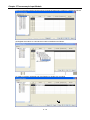
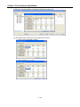
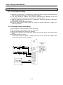
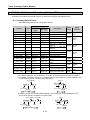
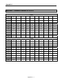
2.13 Example Program
2.13.1 Program to sort A/D converted value in size
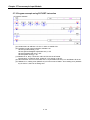
(1) System configuration
(2) Initial setting
No.
Item
1
2
3
4
5
6
Channel
Input voltage range
Output data range
Filter process
Ch0 filter constant
Average process
Average process
method
6
7
Average value
Details
Ch0, Ch1, Ch2
0 ~ 10 V
0 ~ 4000
Ch0
50
Ch1, Ch2
Frequency average: Ch1
Time average: Ch2
Frequency average value:
100 (times)
Time average value:
200 (ms)
Internal memory
address
0
1
2
3
4
12
The value to write in
internal memory
h0007
h0000
h0000
h0001
50
h0006
13
h0100
15
100
16
200
(3) Program
(a) If Ch 0’s digital value is less than 3000, Contact No. 0 (P00080) of relay output module
installed on Slot No.2 will be On.
(b) If CH 1’s digital value is greater than 3200, Contact No.2 (P00082) of relay output module
installed on Slot No.2 will be On.
(c) If CH 2’s digital value is greater than or equal to 3000 and less than or equal to 3200, Contact
No.4 (P00086) of relay output module installed on Slot No.2 will be On.
(d) If CH 2’s digital value is equal to 3200, Contact No.5 (P00085) of relay output module installed
on Slot No.2 will be On.
2 - 34
Chapter 2 Analog Input Module
(4) Program
(a) Program example using [I/O Parameters]
Data no. to read
Read error code
Slot no.
[Program in case of “S” type or “H” type]
2 - 35
Internal Device for
memory
saving
address
Chapter 2 Analog Input Module
]
[Program in case of IEC type]
2 - 36
Chapter 2 Analog Input Module
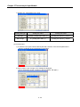
(b) Program example of PUT/GET instruction used
Channel Run signal
[Program in case of “S” type or “H” type]
2 - 37
Chapter 2 Analog Input Module
2 - 38
Chapter 2 Analog Input Module
[Program in case of IEC type]
2 - 39
Chapter 2 Analog Input Module
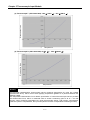
2.14 Troubleshooting
2.14.1 RUN LED flickers
RUN LED flickers.
RUN LED flickers every 0.2 sec.
It seems to be a module defect.
Contact the nearest agency or LS branch office.
Yes
No
RUN LED flickers every 1 sec.
It is Run parameters setting error. Check the error code to
take action against as follows in the table below.
Yes
Error code
(Dec.)
Error Details
Action
50#
Filter constant setting
range exceeded
Change filter constant setting value within 1 ~ 99.
60#
Time average setting
range exceeded
Change time average setting value within 4 ~
16000.
70#
Frequency average
setting range exceeded
Change frequency average setting value within 2
~ 64000.
※ # indicates channel number.
2 - 40
Chapter 2 Analog Input Module
2.14.2 RUN LED is off
RUN LED is off.
A/D conversion module is installed on the base
correctly?
No
Yes
Correctly install A/D conversion module on the base.
.
I/O information can be seen at the XG5000.
Contact the nearest agency or A/S center.
No
Yes
Normally operated if A/D conversion module with
error is changed to another module
Contact the nearest agency or A/S center.
Yes
2 - 41
Chapter 2 Analog Input Module
2.14.3 A/D conversion value is not normal
A/D conversion value is “0”.
Channel status is set as Enable.
Check and correct the channel status on the I/O parameter.
No
Yes
External power (DC 24V) is supplied.
Supply external power (DC 24V)
No
Yes
Wiring of each channel is normal.
Refer to 2.8.2 and wire properly.
No
Yes
Input voltage/current of external terminal
block is normal.
No
Check the status of the external input sensor
2 - 42
Chapter 2 Analog Input Module
2.14.4 Status check of A/D conversion module through XG5000 system monitor
Module type, module information, OS version and module status of A/D conversion module can be
checked through XG5000 system monitoring function.
1) Execution sequence
Two routes are available for the execution.
(1) [Monitor] -> [System Monitoring] -> And on the module screen, click the right mouse button to
display [Module Information].
(2) [Monitor] -> [System Monitoring] -> And Double-click the module screen.
2) Module information
(1)
(2)
(3)
(4)
Module type: shows the information of the module presently installed.
Module information: shows the OS version information of A/D conversion module.
O/S version: shows the OS prepared date of A/D conversion module.
Module status: shows the present error code. (Refer to 7.1 for detailed error codes)
2 - 43
Chapter 3 Analog Output Module
Chapter 3 Analog Output Module
3.1 Setting Sequence before Operation
Before using the analog output module, follow steps below.
XBF-DV04A / XBF-DC04A
Checking performance specification
Specification
z Operating environment
z Digital input range
z Analog output range
System configuration and selection
System configuration
z Max. No. equip-able
z Selecting the external power
Wiring
Wiring
z Wiring (external DC24V)
z Analog output wiring
Checking analog output data
Analog output test
z XG5000 special module monitor
test mode
Setting parameter
Parameter
z XG5000 I/O parameter
Programming
Programming
z Program for writing digital data
(U device)
If there is error or analog output
is abnormal, refer to the trouble shooting.
3-1
Chapter 3 Analog Output Module
3.2 Specification
3.2.1 General specifications
Here describes general specification of analog output module.
No.
Items
Specification
Reference
1
Ambient Temp.
0 ~ 55 °C
2
Storage Temp.
−25 ~ +70 °C
3
Ambient humidity
5 ~ 95%RH (Non-condensing)
4
Storage humidity
5 ~ 95%RH (Non-condensing)
-
Occasional vibration
5
Vibration
-
Frequency
Acceleration
Pulse width
10 ≤ f < 57Hz
−
0.075mm
57 ≤ f ≤ 150Hz
2
Times
−
9.8m/s (1G)
10 times
Continuous vibration
Frequency
Acceleration
each
Pulse width
direction
(X,Y and Z)
10 ≤ f < 57Hz
−
0.035mm
57 ≤ f ≤ 150Hz
2
4.9m/s (0.5G)
−
IEC61131-2
2
• Peak acceleration : 147 m/s (15G)
6
Shocks
• Duration : 11ms
• Pulse wave type : Half-sine (3 times each direction per each axis)
Square wave
±1,500 V
impulse noise
Electrostatic
Voltage: 4kV (Contact discharge)
discharge
7
Impulse noise
LSIS standard
Radiated
electromagnetic
27 ~ 500 MHz, 10V/m
field noise
Fast transient
/Burst noise
8
Operation
ambience
Classifi-
Power
Digital/Analog Input/Output,
cation
supply
Communication Interface
Voltage
2kV
1kV
IEC61131-2
IEC61000-4-2
IEC61131-2,
IEC61000-4-3
IEC61131-2
IEC61000-4-4
Free from corrosive gases and excessive dust
9
Altitude
Less than 2,000m
10
Pollution degree
Less than 2
11
Cooling method
Air-cooling
3-2
-
Chapter 3 Analog Output Module
3.2.2 Performance specifications
Here describes performance specification of analog output module.
Specification
Item
XBF-DV04A
Type
Voltage
Analog
output
Range
DC 0 ~ 10V
(Load resistance: 2kΩ or more)
Type
Digital
input
Range
XBF-DC04A
Current
DC 4 ~ 20mA
DC 0 ~ 20mA
(Load resistance: 510Ω or less)
12-bit binary data
Signed value
0 ~ 4000
0 ~ 4000
Unsigned value
-2000 ~ 2000
-2000 ~ 2000
Precise value
0 ~ 1000
400 ~ 2000/0 ~ 2000
Percentile value
0 ~ 1000
0 ~ 1000
2.5㎷ (1/4000)
5㎂ (1/4000)
Maximum resolution
Accuracy
±0.5% or less
Maximum conversion speed
1㎳/channel
Absolute maximum output
DC ±15V
DC +25㎃
Number of maximum channel
4 channels
Insulation method
Photo-coupler insulation between input terminal and PLC power
(no insulation between channels)
Terminal connected
11-point terminal block
I/O points occupied
Fixed type: 64 points
Current
consump
tion
Internal (DC 5V)
110mA
110mA
External
(DC 21.6 ~26.4V)
70mA
120mA
64g
70g
Weight
Remark
Offset and gain about analog output range have been set at the factory and the user can change them.
3-3
Chapter 3 Analog Output Module
3.3 Designations and Functions
Here describes designation and functions.
XBF-DV04A
RUN
①
CH0
XBF-DC04A
RUN
CH0
②
CH1
CH1
CH2
CH2
CH3
CH3
③
No.
Description
RUN LED
①
It displays the operation status of D/A conversion module
- On: Normal operation status
- Flickering: Error occurred
- Off: Power off or abnormal status of the module
Analog output terminal (Voltage, Current)
②
It is an output terminal to connect an analog output (Voltage, Current) of each
channel to external machinery and tools.
External power input terminal
③
It is an external DC 24V input terminal that supplies power for an analog
output (voltage, current).
3-4
Chapter 3 Analog Output Module
3.4 Characteristic of I/O Conversion
Characteristic of I/O conversion converts a digital input into an analog output (voltage, current) and
displays a straight line with the gradient as shown below. The range of digital input is shown with
Unsigned Value, Signed Value, Precise Value, and Percentile Value such as the graph below.
3-5
Chapter 3 Analog Output Module
3.5 Characteristic of Input/Output
The range of a voltage output is DC 0 ~ 10V and a current output is DC 4 ~ 20mA / DC 0 ~ 20mA.
Digital input value toward analog voltage output is shown below.
Resolution: 2.5mV (1/4000), Accuracy: within ±0.5%
The range of
digital input
Unsigned value
(-48 ~ 4047)
Signed value
(-2048 ~ 2047)
Precise value
(-12 ~ 1011)
Percentile value
(-12 ~ 1011)
Analog voltage output
under 0V
0V
2.5V
5V
7.5V
10V
over 10V
under 0
0
1000
2000
3000
4000
over 4000
under -2000
-2000
-1000
0
1000
2000
over 2000
under 0
0
250
500
750
1000
over 1000
under 0
0
250
500
750
1000
over 1000
Digital input value toward analog current output is shown below.
Resolution: 5μA (1/4000), Accuracy: within ±0.5%
The range of
digital input
Unsigned value
(-48 ~ 4047)
Signed value
(-2048 ~ 2047)
Precise value
(381 ~ 2018, -24 ~ 2023)
Percentile value
(-12 ~ 1011)
Analog current output
under 4mA
4mA
8mA
12mA
16mA
20mA
over 20mA
under 0mA
0mA
5mA
10mA
15mA
20mA
over 20mA
under 0
0
1000
2000
3000
4000
over 4000
under -2000
-2000
-1000
0
1000
2000
over 2000
under 400
400
800
1200
1600
2000
over 2000
under 0
0
500
1000
1500
2000
over 2000
under 0
0
250
500
750
1000
over 1000
3-6
Chapter 3 Analog Output Module
3.6 Accuracy
Though the range of input is changed, the accuracy for the analog output values doesn’t change. The
range of accuracy is displayed at the ambient temperature of 25 ± 5 ℃ if you select unsigned value as
your range of the digital input. The accuracy is satisfied ±0.5%.
10.05V
20.1mA
10V
20mA
9.95V
19.9mA
Analog output
10mA
5V
0.05V
0.1mA
0V
0mA
-0.05V
-0.1mA
0
2000
Digital input
4000
(1) Accuracy in case of 5V output
4000 × 0.5% = 20
So in case of 5V output, accuracy range is (5V - 20×0.0025V) ~ (5V+20×0.0025V) = 1980 ~ 2020.
(2) Accuracy in case of 10V
4000 × 0.5% = 20
So in case of 10V output, accuracy range is (4000-20) ~ (4000+20) = 3980 ~ 4020.
3-7
Chapter 3 Analog Output Module
3.7 Functions of Analog Output Module
Here describes functions of XBF-DV04A/DC04A module.
Function
Operation
channel
Details
1) It sets up Run/Stop of a channel that will operate an analog output.
2) You can save the time of whole operation by stopping unused channels.
The range of
output
1) It sets up the range of an analog output.
2) Analog voltage output module offers one range of output (DC 0 ~ 10V) and
analog current output module offers two (DC 4 ~ 20mA, DC 0 ~ 20mA).
The range of
input data
1) It sets up the range of a digital input.
2) It offers four ranges of a digital input.
The status of
channel output
1) It sets up the output status of a channel when it switches Run to Stop.
2) It offers four types of output status.
3-8
Chapter 3 Analog Output Module
3.8 Wiring
3.8.1 Precautions for wiring
(1) Use separate cable of an A.C. power line and an external output signal of an analog output
module to prevent a surge or inductive noise from the A.C. side.
(2) Select the cable with consideration of an ambient temperature and a permitted current limit. It is
recommended over AWG22 (0.3㎟).
(3) Don’t let the cable at close range to hot devices or materials. And don’t bring it into contact with
oil for a long time. These are the factors of a short circuit occurs unusual operation or damages
devices.
(4) Check the polarity before external power is supplied to the terminal.
(5) It may produce inductive hindrance that is a cause of unusual operations or defects if you wire
the cable with a high-voltage line or a power line.
3.8.2 Wiring example
(1) Wiring example for analog voltage output module
Motor driver etc.
XBF-DV04A
CH0
CH0+
Over 2kΩ
CH0※1
CH1+
D/A
Conversion
circuit
GND
CH1Motor driver etc.
CH2+
CH2-
CH3
CH3+
Over 2kΩ
CH3※1
+15V
DC/DC
Conversion circuit
DC +24V
DC 0V
DC +24V
DC 0V
GND
-15V
(2) Wiring example for analog current output module
Motor driver etc.
XBF-DC04A
CH0
CH0+
Under
510Ω
CH0※1
CH1+
D/A
Conversion
circuit
GND
CH1Motor driver etc.
CH2+
CH2-
CH3
CH3+
Under
510Ω
CH3※1
+15V
DC/DC
Conversion circuit
DC +24V
DC 0V
DC +24V
DC 0V
-15V
※1: Use a 2-core twisted shielded wire.
3-9
GND
Chapter 3 Analog Output Module
3.9 Operation Parameter Setting
You can specify operation parameters of the analog output module through [I/O parameters] menu in
XG5000.
(1) Setting items
For the user’s convenience, XG5000 provides GUI (Graphical User Interface) for parameters setting of
analog voltage/current output module.
Followings are available through [I/O parameters] on the XG5000 project window.
Item
[I/O Parameters]
Details
(1) It specifies the following items for the module operation.
- Channel Enable/Disable
- Analog output range
- Input type
- Channel output type
(2) After the parameters that user specified in XG5000 are downloaded,
they will be saved to a flash memory in the CPU unit..
(2) How to use [I/O Parameters] menu
(a) Run XG5000 to create a project. (Refer to XG5000 program manual for details on how to create
the project)
(b) Double-click [I/O Parameters] on the project window.
(c) Click the slot of the base that contains analog output module in the [I/O Parameter Setting] window.
In the example, the anolog output module is contained in the slot 1.
3 - 10
Chapter 3 Analog Output Module
(d) Click the arrow button then you can see the menu to choose the applicable module. Select the
applicable module.
(e) Double-click the applicable slot that is selected for the parameters setting or click [Details].
(f) A screen will be displayed for you to specify parameters for respective channels as shown below.
Click a desired item to display parameters to set for respective items.
3 - 11
Chapter 3 Analog Output Module
3.10 Special Module Monitoring Function
You can start to test the analog output module connecting by [Online] Æ [Connect] and then click
[Monitor] Æ [Special Module Monitoring] menu in XG5000.
Remark
1) If the program is not displayed normally because of insufficient system resource, you may start
XG5000 again after close the program and other applications.
2) I/O parameters those are specified in the state of [Special Module Monitoring] menu are temporarily
set up for the test. They will be disappeared when the [Special Module Monitoring] is finished.
3) Testing of [Special Module Monitoring] is the way to test the analog output module. It can test the
module without a sequence program.
3.10.1 How to use special module monitoring
Special module monitoring function is described below based on the analog voltage output module (XGFDV04A).
(1) Start of [Special Module Monitoring]
Go through [Online] Æ [Connect] and [Monitor] Æ [Special module Monitoring] to start. If the
status is not online, [Special Module Monitoring] menu will not be activated.
(2) How to use [Special Module Monitoring]
(a) Connecting XG5000 with PLC basic unit, [Special Module List] window will show base/slot
information and types of special module by click [Monitor] Æ [Special Module Monitoring].
Special Module List wiil display the modules that are installed in PLC now.
3 - 12
Chapter 3 Analog Output Module
(b) Select a special module then click [Module Info.] button to display the information as described
below.
(c) Click [Monitor] button in the [Special Module List] window to display the [Special Module
Monitor] window as below
Parameter setting for a test
3 - 13
Chapter 3 Analog Output Module
(d) [Start Monitoring] button will show you digital input data of the operating channel.
Monitoring screen
Details of channel 0
(e) [Test] is used to change the parameters of the voltage output module. You can change the
parameters when you click the values at the bottom of the screen. It is only available when
XGB CPU unit’s status is in [Stop Monitoring].
(f) [Close] is used to escape from the monitoring/test screen.
3 - 14
Chapter 3 Analog Output Module
3.11 Register U devices (special module variable)
Register the variables for each module referring to the special module information that is set in the I/O
parameter. The user can modify the variables and comments.
(1) Registration sequence
(a) Select a special module type in [I/O Parameter Setting] window.
(b) Double-click [Variable/Comment] from the project window.
(c) Select [Edit] Æ [Register U Device].
In case of IEC, select [Edit] Æ[Register special module variable]
3 - 15
Chapter 3 Analog Output Module
(d) Click ‘Yes’.
(e) As shown below, the variables are registered.
3 - 16
Chapter 3 Analog Output Module
(2) Save variables
(a) The contents of ‘View Variables’ can be saved as a text file
(b) Click [Edit] Æ [Export to File].
(c) The contents of ‘View Variable’ are saved as a text file.
(3) View variables in a program
(a) The example of XG5000 is shown below.
(b) Select [View] Æ [Variables]. The devices are changed into variables.
(c) Select [View] Æ [Devices/Variables]. Device and variable both are displayed.
3 - 17
Chapter 3 Analog Output Module
(d) Select [View] Æ [Devices/Comments]. Device and comment both are displayed.
3 - 18
Chapter 3 Analog Output Module
3.12 Internal memory
Describes configuration and function of internal memory
3.12.1 Data I/O area
Address
(‘s’, ‘h’
type)
U0x.00
U0x.01
U0x.02
U0x.03
Describes data I/O area of analog output module
Address
(IEC
Description
Details
type)
F(15) Bit On(1): Module Ready
%UW0.x.0
Module Ready / Error
0~3 Bit On(1): Channel Error
Bit On(1): Channel Run
%UW0.x.1 CH operation information
Bit Off(0): Channel Stop
Bit On(1): Output Allow
%UW0.x.2
Output setting
Bit Off(0): Output Forbid
%UW0.x.3
CH0 digital input value
U0x.04
%UW0.x.4
CH1 digital input value
U0x.05
%UW0.x.5
CH2 digital input value
Remarks
Read
available
Read/Write
available
12-bit binary data
U0x.06
%UW0.x.6
CH3 digital input value
※ In the device assignment, x stands for a slot number that the module is installed
U0x.00
(%UW0.x.0)
B15 B14 B13 B12 B11 B10 B9
B8
B7
B6
B5
B4
B3
B2
B1
B0
Ready
(1) Module Ready/Channel Error information ( ( ) means deice name of IEC type)
(a) U0x.00.F (%UX0.x.15): It will be ON when XGB CPU unit is powered or reset with the condition
that an analog output module has prepared to convert.
(b) U0x.00.0 ~ U0x.00.3 (%UW0.x.0~%UW0.x.3): It is the flags those display error status of each
channel in the analog output module.
—
—
—
—
—
C
H
3
C
H
2
C
H
1
C
H
0
—
—
—
—
—
—
Module Ready
Æ Bit On (1): Ready
Æ Bit Off (0): Not Ready
Error information (bit)
Æ Bit On (1): Error
Æ Bit Off (0): Normal
(2) Channel operation information
(a) This area is used to display the channel being used.
B15 B14 B13 B12 B11 B10 B9
B8
B7
B6
B5
B4
B3
B2
B1
B0
—
—
—
—
—
—
C
H
3
C
H
2
C
H
1
C
H
0
U0x.01
(%UW0.x.1)
—
—
—
—
—
—
Run channel information (bit)
Æ Bit On (1): During Run
Æ Bit Off (0): Operation Stop
3 - 19
Chapter 3 Analog Output Module
(3) Output setting
(a) Each channel can be specified enable/disable the analog output.
(b) If the output is not specified, output of all the channels will be disabled.
B15 B14 B13 B12 B11 B10 B9
B8
B7
B6
B5
B4
B3
B2
B1
B0
—
—
—
—
—
—
C
H
3
C
H
2
C
H
1
C
H
0
U0x.02
—
—
—
—
—
—
(%UW0.x.2)
Output status setting (bit)
Æ Bit On (1): Allowed
Æ Bit Off (0): Forbidden
(4) Digital input
(a) Digital input value can be selected and used within the range of -48~4047, -2048~2047, 12~1011 (381~2018/-24~2023), and -12~1011 based on input type.
(b) If the digital input value is not specified, it will be set to 0.
U0x.03
B15 B14 B13 B12 B11
U0x.04
U0x.05
U0x.06
B10
B9
B8
B7
B6
B5
B4
B3
B2
B1
B0
Digital input Data of CH0
(%UW0.x.3)
Digital input Data of CH1
(%UW0.x.4)
Digital input Data of CH2
(%UW0.x.5)
Digital input Data of CH3
(%UW0.x.6)
Address
(‘S’, ‘H’ type)
Address
(IEC type)
Details
U0x.03
%UW0.x.3
Digital input value of CH0
U0x.04
%UW0.x.4
Digital input value of CH1
U0x.05
%UW0.x.5
Digital input value of CH2
U0x.06
%UW0.x.6
Digital input value of CH3
3 - 20
Chapter 3 Analog Output Module
3.12.2 Setting area of operation parameters
XBF-DV04A
Address
(Dec)
Description
Details
Remarks
Bit On(1): Run
Bit Off(0): Stop
0
Set up the run channel
1
Set up the output voltage range
2
Set up the input data type
3
Set up the output type of CH0
4
Set up the output type of CH1
5
Set up the output type of CH2
6
Set up the output type of CH3
11
12
13
CH0 setting error
CH1 setting error
CH2 setting error
14
CH3 setting error
Bit (00): 0 ~ 10V
Bit (00): 0 ~ 4000
Bit (01): -2000 ~ 2000
Bit (10): 0 ~ 1000
Bit (11): 0 ~ 1000
Read/Write
available
0: outputs the previous value
1: outputs the min. value of output range
2: outputs the mid. value of output range
3: outputs the max. value of output range
Read
available
Error code
XBF-DC04A
Address
(Dec)
Description
Details
Remarks
Bit On(1): Run
Bit Off(0): Stop
0
Set up the run channel
1
Set up the output voltage range
2
Set up the input data type
3
Set up the output type of CH0
4
Set up the output type of CH1
5
Set up the output type of CH2
6
Set up the output type of CH3
11
CH0 setting error
12
CH1 setting error
13
CH2 setting error
14
CH3 setting error
Bit (00): 4 ~ 20mA
Bit (01): 0 ~ 20mA
Bit (00): 0 ~ 4000
Bit (01): -2000 ~ 2000
Bit (10): 400 ~ 2000/0 ~ 2000
Bit (11): 0 ~ 1000
Read/Write
available
0: outputs the previous value
1: outputs the min. value of output range
2: outputs the mid. value of output range
3: outputs the max. value of output range
Read
available
Error code
(1) Setting up the run channel
If the run channel is not specified, all the channels will be set to Stop.
B15 B14 B13 B12 B11 B10 B9
Address “0”
-
—
—
—
—
—
—
B8
—
3 - 21
B7
—
B6
—
B5
—
B4
B3
B2
B1
B0
—
C
H
3
C
H
2
C
H
1
C
H
0
Run channel (bit)
Æ 1: Run
Æ 0: Stop
Chapter 3 Analog Output Module
(2) Setting up the output voltage/current range
The range of analog output voltage is DC 0 ~ 10V and analog output current is DC 4 ~ 20mA, DC
0 ~ 20mA.
B15 B14 B13 B12 B11 B10 B9
Address “1”
-
—
—
—
—
—
—
B8
—
B7
B6
CH 3
B5
B4
CH 2
B3
B2
CH 1
B1
B0
CH 0
Output range (bit)
Æ 00: 0 ~ 10V(4 ~ 20mA)
Æ 01: 0 ~ 20mA
(3) Setting up the input data type
(a) Input type can be specified for respective channels.
(b) If input data type is not specified, all the channels will be set to the range of 0 ~ 4000.
B15 B14 B13 B12 B11 B10 B9
Address “2”
-
—
—
—
—
—
—
B8
—
B7
B6
CH 3
B5
B4
CH 2
B3
B2
CH 1
B1
B0
CH 0
Input data type (bit)
Æ 00: 0 ~ 4000
Æ 01: -2000 ~ 2000
Æ 10: 0 ~ 1000(400 ~ 2000/0 ~ 2000)
Æ 11: 0 ~ 1000
(4) Setting up the output type
(a) It defines an analog output status when XGB CPU unit is stopped.
(b) The range is 0 ~3 and used devices are regarded as Words.
Address “3”
~
Address “6”
B15 B14 B13 B12 B11
-
-
-
-
-
B10 B9
-
B8
B7
B6
B5
B4
B3
B2
-
-
-
-
-
-
-
-
Address
Details
3
Set up the output type of CH0
4
Set up the output type of CH1
5
Set up the output type of CH2
6
Set up the output type of CH3
3 - 22
B1
B0
Value
Input data type (bit)
Æ 00: Previous value
Æ 01: Min. value
Æ 10: Mid. value
Æ 11: Max. value
Chapter 3 Analog Output Module
(5) Error code
It displays error codes of each channel.
Address “11”
~
Address “14”
Address
B15 B14 B12 B11 B11
B8
B7
B6
B5
B4
B3
B2
B1
B0
Error code
Error code (Decimal)
Details
11
CH0 error
12
CH1 error
13
CH2 error
14
CH3 error
Error code
(Dec)
-
B10 B9
Details
LED status
Offset/Gain setting error
Blinks every 2 sec.
31#
Exceed the range of parameter
41#
Exceed the range of digital input
※ # stands for the channel with error found.
3 - 23
Blinks every 1sec.
Chapter 3 Analog Output Module
3.13 Example Program
3.13.1 Analog output program
(1) Program example using [I/O Parameter Setting].
Module ready
CH. Run information
Digital input data
3 - 24
Chapter 3 Analog Output Module
(2) Program example with PUT/GET instruction.
(3) Program example using parameter in case of IEC type
3 - 25
Chapter 3 Analog Output Module
4) Program example using PUT/GET instruction in case of IEC type
3 - 26
Chapter 3 Analog Output Module
3.14 Troubleshooting
3.14.1 RUN LED flickers
RUN LED flickers.
RUN LED flickers every 0.2 sec.
It seems to be a module defect.
Contact the nearest agency or LS branch office.
Yes
No
RUN LED flickers every 1 sec.
It is Run parameters setting error. Check the error code to
take action against as follows in the table below.
Yes
Error Code
(Dec.)
Error Details
Action
31#
Parameter range excess error
Adjust parameter setting range
41#
Digital input value range excess
error
Adjust digital input value range
※ # indicates channel number.
3.14.2 RUN LED is off
RUN LED is Off.
D/A conversion module is installed on the base
correctly?
No
Yes
Correctly install D/A conversion module on the base.
.
I/O information can be seen at the XG5000.
Contact the nearest agency or A/S center.
No
Yes
Normally operated if D/A conversion module with
error is changed to another module.
Contact the nearest agency or A/S center.
Yes
3 - 27
Chapter 3 Analog Output Module
3.14.3 Analog output value is not normal.
D/A conversion value is “0”.
Channel status is set as Enable.
Check and correct the channel status on the I/O parameter.
No
Yes
External power (DC 24V) is supplied.
Supply external power (DC 24V)
No
Yes
Wiring of each channel is normal.
Refer to 2.8.2 and wire properly.
No
Yes
Input voltage/current of external terminal
block is normal.
No
Set U0x.02 to enable the output referring to p3-19
3 - 28
Chapter 3 Analog Output Module
3.14.4 Status check of D/A conversion module through XG5000 system monitor
Module type, module information, O/S version and module status of D/A conversion module can be
checked through XG5000 system monitoring function.
(1) Execution sequence
Two routes are available for the execution.
(a) [Monitor] -> [System Monitoring] -> And on the module screen, click the right mouse button to
display [Module Information].
(b) [Monitor] -> [System Monitoring] -> And Double-click the module screen.
(2) Module information
(a) Module type: shows the information of the module presently installed.
(b) Module information: shows the O/S version information of A/D conversion module.
(c) O/S version: shows the O/S prepared date of A/D conversion module.
(d) Module status: shows the present error code. (Refer to 3.23 for detailed error codes)
3 - 29
Chapter 4 RTD Input Module
Chapter 4 RTD Input Module
4.1 Setting Sequence before Operation
Before using the RTD input module, follow steps below.
XBF-RD04A / XBF-RD01A
Checking performance specification
Specification
z Operating environment
z Digital input range
System configuration and selection
System configuration
z Max. No. equip-able
z Selecting the external power
Wiring
Wiring
z Wiring (external DC24V)
z RTD input wiring
Reading temperature data
RTD input test
z XG5000 special
monitor test mode
Setting parameter
module
Parameter
z XG5000 I/O parameter
Programming
Programming
z Program for writing digital data
(U device)
If there is error or RTD input value is
abnormal, refer to the trouble shooting
4-1
Chapter 4 RTD Input Module
4.2 Specification
4.2.1 General Specifications
Here describes general specifications of RTD input module.
No.
Items
Specification
Reference
1
Ambient Temp.
0 ~ 55 °C
2
Storage Temp.
−25 ~ +70 °C
3
Ambient humidity
5 ~ 95%RH (Non-condensing)
4
Storage humidity
5 ~ 95%RH (Non-condensing)
-
Occasional vibration
5
Vibration
-
Frequency
Acceleration
Pulse width
10 ≤ f < 57Hz
−
0.075mm
57 ≤ f ≤ 150Hz
2
Times
−
9.8m/s (1G)
10 times
Continuous vibration
Frequency
Acceleration
each
Pulse width
direction
(X,Y and Z)
10 ≤ f < 57Hz
−
0.035mm
57 ≤ f ≤ 150Hz
2
4.9m/s (0.5G)
−
IEC61131-2
2
• Peak acceleration : 147 m/s (15G)
6
Shocks
• Duration : 11ms
• Pulse wave type : Half-sine (3 times each direction per each axis)
Square wave
±1,500 V
impulse noise
Electrostatic
Voltage: 4kV (Contact discharge)
discharge
7
Impulse noise
LSIS standard
Radiated
electromagnetic
27 ~ 500 MHz, 10V/m
field noise
Fast transient
/Burst noise
8
Operation
ambience
Classifi-
Power
Digital/Analog Input/Output,
cation
supply
Communication Interface
Voltage
2kV
1kV
IEC61131-2
IEC61000-4-2
IEC61131-2,
IEC61000-4-3
IEC61131-2
IEC61000-4-4
Free from corrosive gases and excessive dust
9
Altitude
Less than 2,000m
10
Pollution degree
Less than 2
11
Cooling method
Air-cooling
4-2
-
Chapter 4 RTD Input Module
4.2.2 Performance specifications
Here describes general specifications of RTD input module.
Specifications
Item
No. of input channel
XBF-RD01A
4 channels
One channel
PT100
JIS C1604-1997
JPT100
JIS C1604-1981 , KS C1603-1991
PT100
-200 ~ 600℃
JPT100
-200 ~ 600℃
PT100
-2000 ~ 6000
JPT100
-2000 ~ 6000
Scaling display
0 ~ 4000
Normal
temp.(25℃)
Within ±0.3%
Full temp.(0~55℃)
Within ±0.5%
Input sensor
type
Temperature
input range
Digital output
Accuracy
XBF-RD04A
Conversion speed
Insulation
40ms / channel
Channel to
Channel
Terminal to PLC
Power
Non-insulation
Insulation (Photo-Coupler)
Terminal block
15-point terminal block
I/O points occupied
Fixed type: 64 points
Wiring method
3-wire
Max. number of equipment
7 (when using XBM-DxxxS “S”type)
10 (when using XB(E)C-DxxxH “H”type)
Filtering
Digital filter (160 ~ 64000ms)
Alarm
Disconnection detection
Inner DC5V
100㎃
external DC24V
100㎃
Function
Current
consumption
Weight
63g
4-3
Chapter 4 RTD Input Module
4.3 Part Names and Functions
Here describes part names and functions.
①
②
⑤
③
④
No.
Descriptions
Name
▶ Displays the hardware operation status of XBF-RD04A
①
RUN LED
On: Normal
Flickering: Error (0.2s flickering)
Off: power disconnected, hardware error
▶Displays the disconnection status of XBF-RD04A
②
ALM LED
③
Terminal
block
(Alarm indication LED)
Flickering: Disconnection is detected (1sec flickering)
Off: normal operation
④
⑤
▶Terminal block for connecting external RTD temperature sensor
External
power supply ▶Terminal for supplying external DC24V
terminal
Connector for
▶Connection connector for connecting extension module
extension
4-4
Chapter 4 RTD Input Module
4.4 Temperature Conversion Characteristic
Since RTD sensor has non-linear characteristic, RTD input module linearizes the relationship between
input and output in each section.
The graph below is an example to describe the linearization process and is different with graph about
sensor temperature input.
(1) PT100: JIS1604-1997
Temperature
(℃)
600.0℃
18.52
0.0℃
Measured temperature
Resistance (Ω)
Linearized sensor characteristics
Real Sensor characteristics
100
313.71
-200.0℃
(2) JPT100: JIS C1604-1981, KS C1603-1991
Temperature
(℃)
600.0℃
17.14
0.0℃
100
-
317.28
Measured temperature
Resistance (Ω)
Linearized sensor characteristics
Real sensor characteristics
Remark
Non-linear characteristics: The resistance-temperature characteristics for RTD sensor are presented
with table (JIS C1604-1997). This characteristics table displays resistance value of the sensor to
temperature, namely, the change of the resistance value per increment of 1℃. When the
temperature is changed by 1℃, the change of resistance is not in constant width but in different
width per section, which is called the non-linear characteristics.
4-5
Chapter 4 RTD Input Module
4.5 Conversion Speed
The conversion speed of XGF-RD4A is 40 ms per channel and each channel is converted
sequentially, that is, one channel is converted and then the next channel is converted.
(Run/stop can be specified independently for each channel.)
The conversion speed includes the time to convert input temperature (resistance value) to digital
value and to save the converted digital data into the internal memory.
∴ Processing time = 40ms X Number of the using channels
[Example] 3 channels are used: Processing time = 40ms X 3 = 120ms
4.6 Accuracy
The accuracy of RTD module is described below.
• When the ambient temperature is 25 ± 5℃: within ±0.3% of available input range
• When the ambient temperature is 0 to 55℃: within ±0.5% of available input range
Example) PT100 is used and the ambient temperature is normal.
To measure 100℃, the conversion data output range:
100℃ - [ { 600 - (-200) } x 0.3 % ] ~ 100℃ + [ { 600 - (-200) } x 0.3 % ]
Namely, 97.6 ~ 102.4 [℃]
4.7 Temperature Display
(1) The input temperature is converted to digital value down to the one decimal place.
Ex.) If the detected temperature is 123.4℃, its converted value to be saved to the internal
memory will be 1234.
(2) Temperature can be converted to Celsius or Fahrenheit scale temperature value as desired.
Ex) If Pt100 sensor is used, the temperature of 100.0℃ can be converted to 2120 when
Fahrenheit scale is used.
9
C + 32
5
5
• Conversion ℉ to ℃, C = (F − 32 )
9
• Conversion ℃ to ℉, F =
(3) Maximum temperature input range is higher/lower within 10℃ than regular temperature input
range. However, the precision will not be guaranteed for any temperature out of regular
temperature input range.
Maximum temperature input ranges of sensor are as follows;
• PT100 : -210.0 ~ 610.0℃
• JPT100 : -210.0 ~ 610.0℃
4-6
Chapter 4 RTD Input Module
4.8 Scaling Function
It is used to scale and output the range specified by the user other than temperature range.
• Scaling expression =
(Temperature × 10 + 2000)
2
Ex.) When scaling is allowed and sensor input is 200℃ with PT100 sensor, scaling value is as follows.
Scaling value =
(200 ×10 + 2000)
2
= 2000
The figure below displays the relation between temperature input and scaling value.
Scaling
conversion
value
4000
2000
-200.0
200.0
0.0
4-7
600.0
Temperature
Conversion value
Chapter 4 RTD Input Module
4.9 Disconnection Detection Function
(1) As a module used to measure the temperature with the RTD temperature sensor directly
connected, it detects and displays disconnection of the sensor connected. If any disconnection
occurs in the sensor used and extended lead wire, LED (ALM) will flicker in a cycle of 1 second
and produce an error code.
(2) Disconnection can be detected per channel, however, only for the channel specified to run.
LED (ALM) is used in common for all the channels. It will flicker if one or more channels are
disconnected.
(3) The figure below shows the temperature sensor’s appearance of the 3-wired RTD.
(The appearance depends on sensor type)
A terminal
A
B terminal
B
b
* A disconnection: if disconnected between terminal A and terminal board of the module in the
sensor figure.
* B disconnection: if disconnected between terminal B (two for 3-wired sensor) and terminal
board of the module in the sensor figure, or if A and B lines are all disconnected.
(4) The basic connection between RTD module and RTD Sensor is based on 3-wired RTD sensor.
If 2-wired or 4-wired sensor is used, the connection between the sensor and the module shall be
kept as 3-wired. Disconnection will be detected on the basis of 3-wired wiring.
(5) In case of disconnection, status of ALD LED and operation of disconnection flag are as follows.
- For disconnection flag, refer to 12.3.14 internal memory.
Connection status
Channel
status
ALM LED
status
Disconnection
flag
Run
Off
Off
Stop
Off
Off
Run
Flicker (1s)
On
Stop
Off
Run
Flicker (1s)
Stop
Off
Normal
A line disconnected or
B line disconnected
Any sensor is not
connected
4-8
Off
On
Off
Chapter 4 RTD Input Module
4.10 Wiring
- 3 types of sensor-connecting methods are available (2, 3 and 4-wired).
- The standard wiring method for XGF-RD4A module is 3-wired wiring.
- Use an identical type of wire (thickness, length, etc.) for each 3 wire when extended lead wire is
used.
- The resistance of each conductor is to be less than 10Ω. (If larger than this, it will cause an error.)
- Resistance difference of each conductor is to be less than 1Ω. (If larger than this, it will cause an
error.)
- Length of wire is to be as short as possible and it is recommended to connect the wire directly to the
terminal block of module without connection terminal unit. If a connection terminal is to be used,
compensating wire shall be connected as shown below.
4.10.1 If 2-wired sensor is used (connection terminal unit is used)
Terminal block
A
B
*2
24V
*1 If sensor and compensating wire are shielded,
shield line can be connected to FG terminal of
the module.
*2 Let the terminals B and b short on the terminal
block of the module if 2-wired sensor is to be
connected.
b
*3
24G
FG
*1
*3 DC 24V external supply terminal to supply the
analog power to module
4.10.2 If 3-wired sensor is used (connection terminal unit is used)
Terminal block
A
B
b
24V
*2
24G
*1 If sensor and compensating wire are shielded,
shield line can be connected to FG terminal of
the module.
*2 DC 24V external supply terminal to supply the
analog power to module
4-9
*1
FG
Chapter 4 RTD Input Module
4.10.3 If 4-wired sensor is used (connection terminal unit is used)
Terminal block
A
B
b
24V
*2
24G
1* If sensor and compensating wire are
shielded, shield line can be connected to FG
terminal of the module.
2* DC 24V external supply terminal to supply
the analog power to module
4 - 10
FG
*1
Chapter 4 RTD Input Module
4.11 Filtering Function
Based on the filter value (time-constant) which defines the temperature-converted value of the specified
channel, it performs and outputs calculation as below.
Filtered temperatur e =
(Previously filtered temp.x Filter value ms ) + (Presently input temp.x40 ms × Channels used)
Filter value ms + (40 ms × Channels used)
Temperature(℃)
Filtered Temperature
Actual temperature
100 ℃
63.2 ℃
0 ℃
Time (ms)
Filtering
Constant (ms)
• Filtering constant setting range = 160 ~ 64000 [ms]
4 - 11
Chapter 4 RTD Input Module
4.12 Operation Parameter Setting
Operation parameters of RTD module can be specified through [I/O parameters] of XG5000.
4.12.1 Setting items
For the user’s convenience, XG5000 provides GUI (Graphical User Interface) for parameters setting
of RTD module. Setting items available through [I/O parameters] of the XG5000 project window are
described below.
Item
Details
[I/O Parameter]
(1) Specify the following setting items necessary for the module operation.
- Channel Run/Stop
- Sensor type
- Filter setting
- Scaling setting
(2) The data specified by user through S/W package will be saved on the
flash memory of RTD module when [I/O Parameters] are downloaded.
4.12.2 How to use [I/O Parameter]
(1) Run XG5000 to create a project. (Refer to XG5000 programming manual for details on how to
create the project)
(2) Double-click [I/O Parameter] on the project window.
(3) If [I/O Parameter Setting] screen appears, click Module part at relevant slot and select relevant
module.
(4) On the ‘I/O parameters setting’ screen, find and click the slot of the base where RTD module is
installed on.
4 - 12
Chapter 4 RTD Input Module
(5) Click the arrow button on the screen to display the screen where an applicable module can be
selected. Search for the applicable module to select.
(6) After the module selected, click [Details] or double-click relevant slot.
(7) A screen will be displayed to specify parameters for respective channels as shown below. Click a
desired item to display parameters to set for respective items.
(8) The initial values of respective items are as follows.
(a) Channel status setting screen
4 - 13
Chapter 4 RTD Input Module
(b) Input sensor type setting screen
(c) Temp. unit setting screen
(d) Scaling setting screen
(9) If necessary setting is complete, press OK.
(10) Check the check box on the parameter menu to select and change setting of a channel then the
setting value of all the channels will be identical to changed setting value. The figure below shows
an example with this function that channel status is changed to ‘Enable’ of all the channels.
4 - 14
Chapter 4 RTD Input Module
4.13 Special Module Monitoring
Run Special Module Monitoring by selecting [On-Line] -> [Connect] and [Monitor] -> [Special Module
Monitoring]. If the status is not [On-Line], [Special Module Monitoring] menu will not be activated.
Remark
1) If the program is not displayed normally because of insufficient system resource, you may start
XG5000 again after close the program and other applications.
2) I/O parameters those are specified in the state of [Special Module Monitoring] menu are temporarily
set up for the test. They will be disappeared when the [Special Module Monitoring] is finished.
3) Testing of [Special Module Monitoring] is the way to test the analog output module. It can test the
module without a sequence program.
4.13.1 How to use special module monitoring
(1) Start of [Special Module Monitoring]
Go through [Online] Æ [Connect] and [Monitor] Æ [Special module Monitoring] to start. If the
status is not online, [Special Module Monitoring] menu will not be activated.
4 - 15
Chapter 4 RTD Input Module
(2) How to use [Special Module Monitoring]
(a) [Special Module List] window will show base/slot information and types of special module by
click [Monitor] Æ [Special Module Monitoring].In this list box, the modules that are now installed in
PLC system will be displayed.
(b) Select a special module then click [Module Info.] button to display the information as
described below.
(c) Select a special module then click [Start Monitoring] button to display the information as
described below.
4 - 16
Chapter 4 RTD Input Module
(d) [Start Monitoring]: [Start Monitoring] button will show you digital input data of the operating
channel. The figure below is monitoring screen when all channels are Run status.
Monitoring screen
Detail of channel 0
[Start Monitoring] execution screen
(e) [Test]: [Test] is used to change the parameters of the RTD input module. You can change the
parameters when you click the values at the bottom of the screen. It is only available when
XGB CPU unit’s status is in [Stop].
[Test] execution screen
(g) [Close]: [Close] is used to escape from the monitoring/test screen. When the monitoring/test
screen is closed, the max. value, the min. value and the present value will not be saved any
more.
Remark
[Test] function is only available when XGB CPU unit’s status is in [Stop].
4 - 17
Chapter 4 RTD Input Module
4.14 Register U devices (Special module variable)
Register the variables for each module referring to the special module information that is set in the I/O
parameter. The user can modify the variables and comments.
(1) Procedure
(a) Select the special module type in the [I/O Parameter Setting] window.
(b) Double click ‘Variable/Comment’ from the project window. .
(c) Select [Edit] – [Register U Device].
In case of IEC, select [Edit] – [Register special module variable]
4 - 18
Chapter 4 RTD Input Module
(d) Click ‘Yes’.
(e) As shown below, the variables are registered.
(2) Save variables
(a) The contents of ‘View Variable’ can be saved as a text file.
(b) Select [Edit] -> [Export to File].
(c) The contents of ‘View variable’ are saved as a text file.
4 - 19
Chapter 4 RTD Input Module
(3) View variables
(a) The example program of XG5000 is as shown below.
(b) Select [View] -> [Variables]. The devices are changed into variables.
(c) Select [View] -> [Devices/Variables]. Devices and variables are both displayed.
(d) Select [View] -> [Device/Comments]. Devices and comments are both displayed.
4 - 20
Chapter 4 RTD Input Module
4.15 Configuration and Function of Internal Memory
Here describes configuration and function of internal memory.
4.15.1 Data I/O area of RTD input module
Data I/O area of RTD input module is as shown below.
Area
(‘S’, ‘H’ type)
U0x.00.0
U0x.00.F
Area
(IEC type)
%UX0.x.0
%UX0.x.15
Module ERROR flag
Module READY flag
U0x.01.0
U0x.01.1
U0x.01.2
U0x.01.3
%UX0.x.16
%UX0.x.17
%UX0.x.18
%UX0.x.19
CH0 Run flag
CH1 Run flag
CH2 Run flag
CH3 Run flag
U0x.01.4
U0x.01.5
U0x.01.6
U0x.01.7
%UX0.x.20
%UX0.x.21
%UX0.x.22
%UX0.x.23
CH0 Disconnection flag
CH1 Disconnection flag
CH2 Disconnection flag
CH3 Disconnection flag
U0x.04
%UW0.x.4
U0x.05
%UW0.x.5
U0x.06
%UW0.x.6
U0x.07
%UW0.x.7
U0x.08
U0x.09
U0x.10
U0x.11
%UW0.x.8
%UW0.x.9
%UW0.x.10
%UW0.x.11
Details
CH0
value
CH1
value
CH2
value
CH3
value
Content
digital
output
digital
output
digital
output
digital
output
R/W
0 Bit On(1): module error
F(15) Bit On(1): module normal
R
Bit On(1): channel run
Bit Off(0): channel stop
R
Bit On(1): Disconnection
Bit Off(0): Normal
R
Temperature value ×10
R
R
R
R
CH0 scaling value
CH1 scaling value
CH2 scaling value
CH3 scaling value
0 ~ 4000
R
R
R
R
※ In the device assigned, x stands for the slot no. on which module is installed.
(1) Module ready/channel error information ( ( ) means device name of IEC type)
(a) U0x.00.F (%UX0.x.15): It will be ON when PLC CPU is powered or reset with A/D conversion
ready to process A/D conversion.
(b) U0x.00.0 ~ U0x.00.3 (%UW0.x.0~%UW0.x.3): It is a flag to display the error status of A/D
conversion module.
Bit8
Bit7
Bit6
Bit5
Bit4
Bit3
Bit2
Bit1
Bit0
—
—
—
—
—
—
—
—
—
Error
(%UW0.x.0)
Bit9
Ready
U0x.00
Bit15 Bit14 Bit13 Bit12 Bit11 Bit10
—
—
—
—
—
Error status
Bit On (1): error, Bit Off (0): normal
Module READY
Bit On (1): normal, Bit Off (0): error
4 - 21
Chapter 4 RTD Input Module
(2) Channel run/stop information
(a) It displays which channel is being used.
bit15
bit14
bit13
bit12
bit11
bit10
bit9
bit8
bit7
bit6
bit5
bit4
bit3
bit2
bit1
bit0
—
—
—
—
—
—
C
H
3
C
H
2
C
H
1
C
H
0
C
H
3
C
H
2
C
H
1
C
H
0
U0x.01
— —
(%UW0.x.1)
Run channel information
Bit On (1): Run
Bit Off (0): Stop
Disconnection information (bit)
Bit On (1): Disconnection
Bit Off (0): Normal
(3) Temperature value
It displays current temperature value. Its form is temperature value ×10.
bit15
bit14
bit13
bit12
bit11
bit10
bit9
bit8
bit7
bit6
bit5
bit4
bit3
bit2
bit1
bit0
U0x.04
CH0 temperature conversion value
(%UW0.x.4)
U0x.05
CH1 temperature conversion value
(%UW0.x.5)
U0x.06
CH2 temperature conversion value
(%UW0.x.6)
U0x.07
CH3 temperature conversion value
(%UW0.x.7)
4 - 22
Chapter 4 RTD Input Module
4.15.2 Operation parameter setting area
Operation parameter setting areas of RTD input module are as follows.
Memory address
Hex.
Dec.
Details
R/W
Remark
0H
0
Channel enable/disable setting
R/W
PUT
1H
1
CH0 sensor type setting
R/W
PUT
2H
2
CH1 sensor type setting
R/W
PUT
3H
3
CH2 sensor type setting
R/W
PUT
4H
4
CH3 sensor type setting
R/W
PUT
5H
5
Temperature display unit setting
R/W
PUT
6H
6
CH0 filter constant setting
R/W
PUT
7H
7
CH1 filter constant setting
R/W
PUT
8H
8
CH2 filter constant setting
R/W
PUT
9H
9
CH3 filter constant setting
R/W
PUT
AH – 11H
10~17
Not used
-
-
12H
18
Scaling setting
R/W
PUT
13H - 43H
19~67
Not used
-
-
44H
68
CH0 disconnection information (code)
R/W
GET
45H
69
CH1 disconnection information (code)
R/W
GET
46H
70
CH2 disconnection information (code)
R/W
GET
47H
71
CH3 disconnection information (code)
R/W
GET
(1) Run channel setting
If Run channel is not specified, all channels will be stop status.
bit15
bit14
bit13
bit12
bit11
bit10
bit9
bit8
bit7
bit6
bit5
bit4
bit3
bit2
bit1
bit0
—
—
—
—
—
—
—
—
—
—
C
H
3
C
H
2
C
H
1
C
H
0
Address 0
— —
Setting channel to use (bit)
Bit On (1): Run, Bit Off (0): Stop
(2) Sensor type setting
If it is not specified manually, all channels will be specified as Pt100.
bit15
bit14
bit13
bit12
bit11
bit10
bit9
bit8
bit7
bit6
bit5
Address 1
Ch0 sensor type setting
Address 2
Ch1 sensor type setting
Address 3
Ch2 sensor type setting
Address 4
Ch3 sensor type setting
Word
0
1
bit4
bit3
Description
Specified as PT100
Specified as JPT100
4 - 23
bit2
bit1
bit0
Chapter 4 RTD Input Module
(3) Setting temperature display unit
Unit of temperature conversion value can be specified as Celsius/ Fahrenheit.
bit15
bit14
Bit13
bit12
bit11
bit10
bit9
bit8
bit7
bit6
bit5
bit4
bit3
bit2
bit1
Bit0
—
—
—
—
—
—
—
—
—
—
C
H
3
C
H
2
C
H
1
C
H
0
Address 5
— —
Bit
0
1
Description
Celsius
Fahrenheit
(4) Setting filter constant
If filter constant is not specified or specified as “0”, relevant channel is not filtered.
bit15
bit14
bit13
bit12
bit11
bit10
bit9
bit8
bit7
bit6
bit5
bit4
Address 6
Setting Ch0 filter constant (1~99)
Address 7
Setting Ch1 filter constant (1~99)
Address 8
Setting Ch2 filter constant (1~99)
Address 9
Setting Ch3 filter constant (1~99)
bit3
bit2
bit1
bit0
(5) Setting scaling
It specifies whether scaling function is used or not.
bit15
bit14
bit13
bit12
bit11
bit10
bit9
bit8
bit7
bit6
bit5
bit4
bit3
bit2
bit1
bit0
—
—
—
—
—
—
—
—
—
—
C
H
3
C
H
2
C
H
1
C
H
0
Address 10
— —
Bit
0
1
Description
Scaling function is not used
Scaling function is used
(6) Disconnection information
It outputs disconnection information of each channel.
bit15
Address 68
Address 69
Address 70
Address 71
bit14
bit13
bit12
bit11
bit10
bit9
bit8
bit7
bit6
bit5
bit4
bit3
bit2
bit1
bit0
Channel 0 disconnection information
(0: normal,1: sensor A disconnection, 2: sensor B disconnection)
Channel 1 disconnection information
(0: normal,1: sensor A disconnection, 2: sensor B disconnection)
Channel 2 disconnection information
(0: normal,1: sensor A disconnection, 2: sensor B disconnection)
Channel 3 disconnection information
(0: normal, 1: sensor A disconnection, 2: sensor B disconnection)
4 - 24
Chapter 4 RTD Input Module
4.16 Example Program
- Here describes how to specify the operation condition of RTD input module.
- RTD input module is installed on slot 2.
- Initial setting condition is that with one input, initial setting value is saved in internal memory of
module.
- The following program is an example to read temperature value and disconnection information.
(1) Program example using [I/O Parameter Setting]
Moving channel 0 temp. value to
D0 area
Moving channel 1 temp. value to
D1 area
Moving channel 0 disconnection
information to M0
Moving channel 1 disconnection
information to M1
4 - 25
Chapter 4 RTD Input Module
(2) Program example using PUT/GET command
CH Enable
Sensor type (PT100)
Temperature unit (Celsius)
Filter value
Moving channel 0
temp. value to
Moving channel 1
temp. value to
Moving channel 0 disconnection
information to M0
Moving channel 1 disconnection
information to M
(3) Program example using parameter in case of IEC
4 - 26
Chapter 4 RTD Input Module
(4) Program example using PUT/GET function block inn case of IEC
4 - 27
Chapter 4 RTD Input Module
4.17 Trouble Shooting
4.17.1 RUN LED flickers
RUN LED flickers.
RUN LED flickers every 0.2 sec.
Yes
Contact the nearest agency or LS branch office.
4.17.2 RUN LED is off
RUN LED is off.
RTD input module is installed on the base correctly?
No
Correctly install A/D conversion module on the base.
Yes
I/O information can be seen at the XG5000.
Contact the nearest agency or LS branch office.
No
Yes
Normally operated if RTD input module with error is
changed to another module
Contact the nearest agency or LS branch office.
Yes
4 - 28
Chapter 4 RTD Input Module
4.17.3 ALM (Alarm) LED flickers
ALM LED flickers.
3 wired wiring is normal.
No
Wire properly referring to 4.10
.
Yes
Wiring to sensor is normal
No
Wire properly referring to 4.10
Yes
Contact the nearest agency or A/S center.
4.17.4 Temperature conversion value is not normal.
Temperature conversion value is not normal.
External DC 24V input power is normal.
No
Supply external power (DC 24V)
Yes
FG ground is normal.
No
Execute FG ground properly referring to 4.10
Yes
Contact the nearest agency or A/S center.
4 - 29
Chapter 4 RTD Input Module
4.17.5 Stats check of RTD input module through XG5000 system monitor
Module type, module information, O/S version and module status of RTD input module can be
checked through XG5000 system monitoring function.
(1) Execution sequence
Two routes are available for the execution.
(a) [Monitor] -> [System Monitoring] -> And on the module screen, click the right mouse button to
display [Module Information].
(b) [Monitor] -> [System Monitoring] -> And Double-click the module screen.
(2) Module information
(a) Module type: shows the information of the module presently installed.
(b) Module information: shows the O/S version information of module.
(c) O/S version: shows the O/S prepared date of module.
(d) Module status: shows the present error code.
4 - 30
Chapter 5 Thermocouple Input Module
Chapter 5 Thermocouple Input Module
5.1 General
Here describes specification, handling, programming of XGB thermocouple input module (XBFTC04S).
Thermocouple input module is used to convert the temperature data detected from thermocouple to
signed 16 bit data.
5.1.1 Characteristic
(1) Module selection according to purpose
XBF-TC04S: 4 channel input (Insulation between channels by photo-moth relay)
(2) Four kinds of thermocouple available (K / J / T / R)
Available to select the different thermocouple according to each channel
(3) Disconnection detection
If thermocouple is disconnected, it is detected and indicated.
(4) Celsius (℃)/ Fahrenheit (℉) type available
Temperature conversion data of Celsius (℃)/ Fahrenheit (℉) is indicated down to one decimal
place
(5) Temperature data scaling function
(Available to use it as additional data than temperature indication)
Scaling conversion of temperature data is available within -32,768~32,767/0~65,535.
(6) Various additional function
Filter process, Average process (time/count/moving), Max./Min. detection process
(7) Parameter setting / Monitoring by GUI (Graphical user interface) method
It enhanced user-friendly features by changing to I/O parameter settings (intensify user
interface) from parameter settings by previous instructions.
By [I/O Parameter], the sequence program can be reduced and by [Special Module Monitoring],
it is easy to monitor the temperature conversion value.
5.1.2 Required version
When making the system, the version below is required.
Basic unit type
‘S’, ‘H’ type
IEC type
Classification
Required version
XGB basic unit
Ver 1.8 or above
XG5000
Ver 2.2 or above
XGB basic unit (IEC type)
Ver 1.0 or above
XG5000
Ver 3.0 or above
5-1
Chapter 5 Thermocouple Input Module
5.1.3 Setting sequence before operation
Before using the thermocouple input module, follow steps below.
XBF-TC04S
Checking performance specification
Specification
- Operating environment
- Thermocouple sensor type and temperature
range
- Digital output range
System configuration and selection
System configuration
- Equip-able number
- External power selection
Wiring
Wiring
- Power wiring (External DC24V)
- Thermocouple input wiring
Reading temp. data
Thermocouple input test
- XG5000 special module monitor
Setting parameter
Parameter
- XG5000 I/O parameter
Programming
Programming
- Program to read analog data
(U device)
If there is error or thermocouple input data
is abnormal, refer to the trouble shooting.
5-2
Chapter 5 Thermocouple Input Module
5.2 Specification
5.2.1 General specification
General specifications are as follows.
No.
1
2
3
4
Items
Related
standards
Specification
Operating
temp.
Storage
temp.
Operating
humidity
Storage
humidity
0 ~ 55 °C
−25 ~ +70 °C
5∼95%RH (Non-condensing)
5∼95%RH (Non-condensing)
For discontinuous vibration
Frequency
10 ≤ f
5
Vibration
<
57Hz
57 ≤ f ≤
150Hz
-
Acceleration
Amplitude
−
0.075mm
9.8m/s2(1G)
−
For continuous vibration
Frequency
10 ≤ f
6
7
8
9
10
11
Shocks
Noise
Ambient
conditions
Operating
height
Pollution
degree
Cooling type
<
57Hz
Acceleration
Amplitude
−
0.035mm
Number
Each 10
times in
X,Y,Z
directions
57 ≤ f ≤
4.9m/s2(0.5G)
−
150Hz
• Max. impact acceleration : 147 m/s2(15G)
• Authorized time : 11ms
• Pulse wave : Sign half-wave pulse (Each 3 times in X,Y,Z
directions)
Square wave
±1,500 V
impulse noise
Electrostatic
Voltage : 4kV(contact discharging)
discharging
Radiated
electromagnetic
27 ~ 500 MHz, 10V/m
field noise
Digital/
Power
Fast
Analog I/O
Class
module
Transient
communication interface
/burst
noise
Voltage
2kV
1kV
No corrosive gas or dust
2000m or less
2 or less
Natural air cooling
5-3
IEC61131-2
IEC61131-2
LSIS standard
IEC61131-2
IEC61000-4-2
IEC61131-2,
IEC61000-4-3
IEC61131-2
IEC61000-4-4
Chapter 5 Thermocouple Input Module
5.2.2 Performance Specification
Performance specifications are as follows
Items
Specification
Number of input channel
4 channels
Thermocouple K / J / T / R type
Type of input sensor
JIS C1602-1995
K
-200.0℃ ~ 1300.0℃
Range of input
J
-200.0℃ ~ 1200.0℃
temperature
T
-200.0℃ ~ 400.0℃
R
0.0℃ ~ 1700.0℃
Displaying down to one decimal place – note1)
Temp. display
Digital output
K, J, T type: 0.1℃, R type: 0.5℃
Scaling display
Unsigned scaling (0 ~ 65535)
(user-defined scaling)
Signed scaling (-32768 ~ 32767)
Ambient temperature(25℃)
Within ±0.2% – note 2)
Accuracy
Temp. coefficient
(range of operating temp)
Conversion velocity
Insulation
method
50ms / channel
Terminal – inner circuit
Photo-coupler insulation
Terminal – operating power
DC/DC converter insulation
Between channels
Photo-moth relay insulation
Insulation
400 V AC, 50/60 Hz, 1min,
Insulation pressure
leakage current 10㎃ or below
Insulation resistance
Standard contact
point
compensation
±100 ppm/℃
500 V DC, 10 MΩ or below
Auto compensation by RJC sensing (Thermistor)
±1.0℃
Compensation amount
Warming-up time
15 min or above –note 3)
Terminal block
11 point terminal
I/O occupied points
64 points
Max. number of equipment
7 (when using XBM-DxxxS “S”)
10 (when using XB(E)C-DxxxH “H”)
Digital filter (200 ~ 64,000㎳)
Filter process
Time average (400~64,000㎳)
Average process
Count average (2~64,000 times)
Additional function
Moving average (2~100)
Alarm
Disconnection detection
Max./Min. display
Display Max./Min.
Scaling function
Signed scaling / Unsigned scaling
Consumption
Inner DC5V
100㎃
current
External DC24V
100㎃
Weight
63g
5-4
Chapter 5 Thermocouple Input Module
Note1), Note2) For more detail specification, refer to 5.2.6 accuracy/resolution.
Note 3) Warming-up time: for stability of measured temperature, 15 min is necessary after power is on.
5.2.3 Name of part and function
Respective designations of the parts are as described below
①
②
⑤
③
⑥
④
No.
①
②
③
④
⑤
⑥
Name
RUN LED
ALM LED
Description
▶ Displays the status of thermocouple input module
On: operation normal
Flickering: Error occurs (0.2s flickering)
Off: power Off or module error
▶ Displays the disconnection status of thermocouple input
module (Alarm indication LED)
Flickering: Disconnection error occurs (1s flickering)
Off: operation normal
▶ Terminal block for wiring to connect the thermocouple
(K, J, T, R type)
Terminal
block
External
power supply ▶Terminal for supply of external DC24V
terminal
Connector for
▶Connection connector for connecting the extension module
extension
Reference
junction
▶ Thermistor for reference junction compensation (RJC)
compensator
5-5
Chapter 5 Thermocouple Input Module
5.2.4 Characteristic of thermocouple temperature conversion
Thermocouple input module connect 4 kinds of thermocouple directly, input characteristic are as
described below.
Electromotive force
(1) Thermocouple K (JIS C1602-1995): -200 ℃(-5891 ㎶) ~ 1300 ℃(52410 ㎶)
Temperature
Electromotive force
(2) Thermocouple J (JIS C1602-1995): -200 ℃(-7890 ㎶) ~ 1200 ℃(69553 ㎶)
Temperature
5-6
Chapter 5 Thermocouple Input Module
Electromotive force
(3) Thermocouple T (JIS C1602-1995): -200 ℃(-5603 ㎶) ~ 400 ℃(20872 ㎶)
Temperature
Electromotive force
(4) Thermocouple R (JIS C1602-1995): 0 ℃(0 ㎶) ~ 1700 ℃(20222 ㎶)
Temperature
Remark
Thermocouple characteristics: thermocouple sensor measures temperature by using fine voltage
(electromotive force), which occurs when applying temperature gradient to a junction between two
different metals.
The temperature-electromotive force relation specification of normal thermocouple sensor provides
the electromotive force, which is measured when a sensor’s measuring point is at O℃. On that
account, when measuring temperature by using thermocouple sensor, cold junction compensation
(reference junction compensation, RJC) is used. (built-in function of temperature measuring module).
5-7
Chapter 5 Thermocouple Input Module
(5) Temperature conversion characteristic
Thermocouple input module converts the thermocouple input with non-linear characteristics into A/D
and outputs the temperature conversion that is linearly treated.
Temperature conversion to thermocouple input has non-linear characteristics.
Remark
Non-linear characteristics: regarding the relation of temperature(℃) and electromotive force(㎶) of a
thermocouple sensor, electromotive force is different by sections even though temperature changes
by a certain amount, which is called ‘non-linear characteristics.’ As seen in the above graph, it is
shown that the relation of temperature and electromotive force is a curve by temperature sections.
The module processes the non-linear characteristics table as linear.
5.2.5 Temperature display
(1) Temperature is displayed down to one decimal place.
In the XG5000, when monitoring the temperature conversion value, select “Signed decimal”
According to monitor indication type, temperature is monitored like figure below.
Ex.) if displaying -123.0℃ by converting, the value stored in the internal memory would
be -1230.
Monitor indication type
Unsigned decimal
Signed decimal
Indication
contents
64306
Temperature indication value
(Inner memory)
-123.0℃
Temperature
value
-1230
(-123.0℃)
Hexadecimal
hFB32
As instruction
64306
-1230
(2) Temperature display unit
(a) K, J, T type: 0.1℃
(b) R type: 0.5℃
(3) Temperature may be displayed by Celsius or Fahrenheit, depending on the settings.
Ex.) if displaying 100 ℃ in Fahrenheit, it would be 212 F
° by using the following formula.
9
F = C + 32
5
5
(b) From Fahrenheit to Celsius degree C = (F − 32 )
9
(a) From Celsius to Fahrenheit degree
5-8
Chapter 5 Thermocouple Input Module
5.2.6 Accuracy / Resolution
Accuracy / Resolution are as follows according to ambient temperature
Measurement
Thermocouple
temperature
type
range
K
-200.0℃ ~
1300.0℃
J
-200.0℃ ~
1200.0℃
T
-200.0℃ ~
400.0℃
R
0.0℃ ~
1700.0℃
Indication temperature
range
-270.0℃ ~ -200.0℃
-200.0℃ ~ 0.0℃
0.0℃ ~ 1300.0℃
1300.0℃ ~ 1372.0℃
-210.0℃ ~ -200.0℃
-200.0℃ ~ -100.0℃
-100.0℃ ~ 1200.0℃
-270.0℃ ~ -200.0℃
-200.0℃ ~ 400.0℃
-50.0℃ ~ 0.0℃
0.0℃ ~ 1700.0℃
1700.0℃ ~ 1768.0℃
Accuracy - note1)
Operating
Normal
temperature temperature
note2)
(25℃)
(0℃ ~ 55℃)
- note3)
±3.0℃
±7.5℃
±3.0℃
±7.5℃
- note3)
- note3)
±2.8℃
±7.0℃
±2.8℃
±7.0℃
- note3)
±1.2℃
±3.0℃
- note3)
±3.5℃
±8.5℃
- note3)
resolution
0.2℃
0.1℃
0.2℃
0.1℃
0.1℃
0.5℃
Note1) Total accuracy (normal temp.) = accuracy (normal temp.) + cold junction compensation accuracy
= ±(full scale X 0.2% + 1.0℃)
Cold junction compensation accuracy = ±1.0℃
Note2) Temp. coefficient: ±100 ppm/℃
Note3) Measuring the temp. is available, but accuracy and resolution is not guaranteed.
(1) When ambient temp. is normal (25 ± 5℃): within the ±0.2% range of measurement temp.
(2) When ambient temp. is operating temp. (0 ~ 55℃): within the ±0.5% range of measurement temp.
Ex.) When K type thermocouple is used and ambient temperature is normal.
In case of measuring 1000℃ temperature, output range of conversion data is
1000℃ - [{1300 - (-200)} x 0.2 %] - 1 ~ 1000℃ + [{1300 - (-200)} x 0.2 %] + 1
namely, 996.0 ~ 1004.0 [℃].
Note
(1) For stabilization of measurement temperature, warming-up time more than 15 min. is necessary, after
restart.
(2) If ambient temperature changes rapidly, measurement temperature may change temporally. Keep the
ambient temperature steady for stabilization of measuring temperature.
(3) If wind of the cooling pan contacts with module directly in the panel, accuracy decreases. Do not
contact with wind directly.
5-9
Chapter 5 Thermocouple Input Module
5.2.7 Conversion velocity
(1) Conversion velocity per channel: 50ms/channel
(2) Sequential process method
The next channel is converted after conversion of one channel is completed.
(Run/Stop of the respective channels can be set independently.)
(3) Concept of conversion time
The conversion velocity of XGF-TC4S module is a cycle that the temperature (electromotive
force) entered into terminal strip is converted into digital value and stored in internal memory.
Conversion time increase by a multiple of the no. of used channels
∴ Conversion time = 50ms X no. of used channels
Ex.) In case 3 channels is used: conversion time = 50ms X 3 = 150ms
Channel 0
Conversion
Channel 1
Conversion
Repetition
Conversion
Channel 2
Conversion
Channel0
Conversion
channel1
Conversion
channel2
Conversion
50ms
50ms
50ms
150ms
5 - 10
channel0
Conversion
Chapter 5 Thermocouple Input Module
5.3 Function
5.3.1 Disconnection detection function
Thermocouple input module has a function to detect the disconnection and display it.
That the module detects and displays disconnection means that the following cabling path would have
partially bad connection, which requires taking measures
(1) Disconnection occurs between a sensor used/compensating cable and module, LED(ALM) flickers
every second and generates error code.
(2) Disconnection can be detected by channels. However, it is available for the only channel(s)
designated for operation. LED (ALM) is commonly used for every channel. It flickers in case even
only one channel is disconnected.
Thermocouple connection
status
Normal
Thermocouple
disconnection
Channel
run
ALM LED
status
Disconnection
flag
Run
Off
Off
Stop
Off
Off
Run
Flickering (1s)
On
Stop
Off
Off
(3) In case disconnection occurs, disconnection flag of each channel will be turned on and in case
disconnection is canceled, it will be turned off.
Disconnection flag
Contents
U0x.01.4
Ch. 0 disconnection
U0x.01.5
Ch. 1 disconnection
U0x.01.6
Ch. 2 disconnection
U0x.01.7
Ch. 3 disconnection
(4) When disconnection occurs, the min value among range is displayed.
Type
Displayed temperature in case of disconnection
K type
-270.0℃
J type
-210.0℃
T type
-270.0℃
R type
-50.0℃
5 - 11
Chapter 5 Thermocouple Input Module
5.3.2 Scaling function
Thermocouple input module has a function to scale value in user-defined range besides temperature
display.
The scope is classified into two types; 16 bits data type, -32768~32767 and 16 bits data type without
mark, 0~65535.
If a user selects one of these two types and sets the range, it displays the temperature through scaling
operation.
Scaling data type
Scaling min. value
Scaling max. value
Signed value
-32768 ~ [Scaling max. value -1]
[Scaling min. value+1] ~ 32767
Unsigned value
0 ~ [Scaling max. value-1]
[Scaling min. value+1] ~ 65535
The following graph indicates relation between scaled value and temperature input.
Scaling
Conversion
value
Y1
13000
Y
5000
X0
-200.0
1300.0 Temperature
500.0
X
-2000
Y0
Scaling operation: Y =
X1
value
(Y1 − Y0)
(X − X0) + Y0
(X1 − X0)
X = Temperature value
X0 = Thermocouple measurement min. temperature value
X1 = Thermocouple measurement max. temperature value
Y0 = Scaling min. value
Y1 = Scaling max. value
Y = Scaling
Ex.) If scaling with mark is set with -2000 ~ 13000 and the temperature measured K type sensor is
500.0℃, the value scaled is as follows.
• Scaling conversion value =
(13000 − (−2000))
(500 − (−200)) + (−200) = 5000
(1300 − (−200))
5 - 12
Chapter 5 Thermocouple Input Module
5.3.3 Filter function
By means of filter value (time constant 63.2%) setting temperature conversion of a designated
channel, it operates and outputs as follows.
Filtered temp. value =
(previously filtered temp. value × fileter value ms ) + (presen input temp. value x 50 ms × No.of channel used)
Filter value ms + (50 ms × No.of channels used)
Filter constant setting range = 200 ~ 64000 [ms]
Temperature (℃)
Temperature change after filtering process
Actual temperature change
100 ℃
63.2 ℃
0 ℃
Time (ms)
Filter constant
(ms)
5 - 13
Chapter 5 Thermocouple Input Module
5.3.4 Average function
(1) Time average
It accumulates temperature conversion values of a selected channel and displays the average
of the total sum in digital data.
Temperature change after averaging process
Actual temperature change
Channel scan interval
Averaging section
Averaging section
Averaging section
Setting range of average time = 400 ~ 64000 [ms]
Frequency of average process for a preset time can be calculated as follows.
Average Process Frequency [times] =
Average time ms
No. of channel used × 50 ms
(2) Averaged frequency
It accumulates temperature conversion values of a selected channel as many as frequency and
displays the average of the total sum in digital data.
Temperature change after averaging process
Actual temperature change
Channel scan interval
Averaging section
Averaging section
Averaging section
Setting range of average frequency = 2 ~ 64000 [times]
Average process interval of channel used can be calculated as follows
Average process interval[ms] = Average frequency × No. or channel used × 50[ms]
5 - 14
Chapter 5 Thermocouple Input Module
(3) Moving average
It accumulates temperature conversion values of a selected channel as many as set and
displays the average of the total sum in digital data. In case of the moving average, it outputs
average per scan.
Setting range of average number = 2 ~ 100
Average
Average
Average
Channel scan interval
Remark
(1) time/frequency average characteristically does not output temperature data every conversion time
and instead, it keeps a feature to maintain the previous status until it reaches time/average
frequency.
(2) In case of moving average, it outputs the converted temperature as taking temperature history and
average, which are entered previously, every conversion time, so it can obtain relatively faster data
response than time/frequency average.
(3) Filtering can be processed with one of the foresaid averaging functions simultaneously. If
simultaneous process is selected, filtering would be processed first and it averages and output
temperature value in digital value. At the moment, the digital data output (temperature) is displayed
as the value gained after the final process.
5.3.5 Max./Min. display
It displays maximum/minimum value of temperature conversion value of a selected channel for a
selected section (a section allowed for max./min. search)
Status of command allowing/prohibiting max./min. search
Maintaining previous
max./min. value
Maintaining previous
max./min. value
Display max./min. value
Display max./min. value
Initializing max./min. value
Initializing max./min. value
5 - 15
Chapter 5 Thermocouple Input Module
5.4 Installation and Wiring
5.4.1 Installation environment
Although the device can be installed with high reliance regardless of installation environment, attention
should be paid to the followings in order to secure the reliance and stability of the system.
(1) Environmental Conditions
(a) Install on a water-proof and dust-proof control board.
(b) Place free of continuous impact or vibration.
(c) Place not directly exposed to direct sunrays.
(d) Place where dew does not form due to rapid temperature change.
(e) Place where ambient temperature is maintained between 0 - 55℃.
(2) Installation Construction
(a) In case of screw hole processing or wiring construction, wiring dregs should not go into PLC.
(b) Install on a position easy to access.
(c) Should not install on the same panel which high voltage device is installed on.
(d) It should be 50mm and longer distant from duct and modules.
(e) Should ground in the environment where is not interrupted from noise.
(f) Install not to contact with cooling pan in the panel
(3) Cautions in handling
It describes caution in handling from unpacking module to installation.
(a) Do not fall or apply excessive impact on it.
(b) Never attempt to separate PCB from the case.
(c) Make sure that any impurities including wiring dregs should not go into the upper part of
module during wiring work.
(d) Never attempt to attach or detach the module when it is turned on.
5.4.2 Wiring
(1) Cautions in wiring
(a) Do not place AC power line close to the AUX signal line of the module. To avoid surge or
induced noise occurring from AC, make sure to leave a proper space.
(b) Cable should be selected by considering ambient temperature and allowable current and the
specification of cable should be as follows.
Cable specification
Lower limit
Upper limit
0.18mm2 (AWG24)
1.5 mm2 (AWG16)
(c) If cable is placed too close to any heating device or materials or if it directly contacts oil and
similar materials for a long time, it may cause short-circuit, resulting in breakdown and
malfunction.
(d) Check the polarities during terminal strip wiring
(e) Wiring with high voltage cable or power line may cause induction problem, causing malfunction
or trouble.
(f) External DC24V power should be same with power of XGB. If external DC24 V power of
thermocouple input module is turned on/off while power of XGB main unit is on, temperature
input value may have an error.
(g) Thermocouple input module may use 4 types of thermocouple sensors. (K / J / T / R)
5 - 16
Chapter 5 Thermocouple Input Module
(2) Terminal array
Terminal array of thermocouple input module is as follows.
Signal
name
CH0 +
CH0 CH1 +
CH1 CH2 +
CH2 CH3 +
CH3 NC
DC24V+
DC24V-
Purpose
Channel 0 thermocouple input
Channel 1 thermocouple input
Channel 2 thermocouple input
Channel 3 thermocouple input
Not used
For external DC24V power
(3) Wiring example
Thermocouple can be connected with module directly. If point where temperature is measured is
far from the module, use the compensating cable to connect
(The compensating cables are different according to thermocouple type. For more information
about the compensating cable, contact the producer of thermocouple.)
1) In case sensor and compensating cable are shielded, shield connection is possible to PLC FG terminal.
2) It is necessary to use extension terminal block of which material is kept at uniform temperature in order
to reduce error.
3) Compensating cable should use the same type of sensor, which was used for measuring.
5 - 17
Chapter 5 Thermocouple Input Module
5.5 Operation Setting and Monitor
5.5.1 Operation Parameter Setting
Operation parameter of thermocouple input module can be set through [I/O Parameter] of XG5000.
(1) Setting items
For user convenience, parameter setting of thermocouple input module is provided by GUI
(Graphical User Interface) method in the XG5000. The items which can be set through [I/O
Parameter] in the project window are as follows.
Items
[I/O Parameter]
Content
(a) Sets the following items for operation of module.
1) Channel status (Disable / Enable)
2) Sensor status (K / J / T / R)
3) Filter constant
4) Average processing (Sampling / Time-Avr. / Count-Avr. / Moving-Avr.)
5) Scaling data type (Bipolar / Unipolar)
6) Scaling min./max. value
(b) The parameter set by the user is saved in the flash memory of XGB main
unit after download.
(2) How to use [I/O Parameter]
(a) Execute the XG5000 and make the project.
(For how to make the project, refer to the XG5000 user manual)
(b) Double-click [I/O Parameter] on the project window.
5 - 18
Chapter 5 Thermocouple Input Module
(c) If [I/O Parameter Setting] window shows, find slot of base where module is installed and click it.
(d) Register the module on a slot where module is installed on as follows.
(e) Select a module registered and click [Details] or double-click a module
5 - 19
Chapter 5 Thermocouple Input Module
(f) Select the required settings in Parameter Settings and click [OK].
(g) The initial values of each item are as figure shown below
1) Channel status (Disable / Enable)
2) Sensor status (K / J / T / R)
5 - 20
Chapter 5 Thermocouple Input Module
3) Temp. unit (Celsius / Fahrenheit)
4) Filter constant (0, 200 ~ 64000)
5) Average processing (Sampling / Time-Avr / Count-Avr / Moving-Avr)
6) Scaling data type (Bipolar / Unipolar)
5 - 21
Chapter 5 Thermocouple Input Module
7) Scaling min. value/scaling max. value
Scaling data type
Scaling min value
Scaling max value
With sign
-32768 ~ [scaling max value -1]
[scaling min value+1] ~ 32767
Without sign
0 ~ [scaling max value -1]
[scaling min value+1] ~ 65535
(h) Constant input
1) In case the user inputs numbers directly like filter constant, if the relevant parameter is
selected, available range is displayed in the bottom.
2) If the number is out of range, error message is displayed.
(If error information shows, it returns to previous status. Set again.)
5 - 22
Chapter 5 Thermocouple Input Module
3) If the wrong number is specified, it is displayed with red color.
(When Average value or scaling min./max. value is out of range.)
5.5.2 Special module monitoring function
While XG5000 is connected with PLC, through [Monitor] -> [Special Module Monitoring], the user can
test the operation of the analog output module.
Remark
1) If system resource is short, the screen may not be displayed properly. In case of this, shut down
other application program and restart the XG5000.
2) On the [Special Module Monitoring] status, I/O parameter is set temporarily to execute the test. So
if [Special Module Monitoring] status ends, I/O parameter is not saved.
3) By test function of [Special Module Monitoring], the user can check if analog module operates
properly or not without any sequence program.
(1) How to use special module monitoring
(a) Start of [Special Module Monitoring]
While XG5000 is connected with PLC, start [Monitor] -> [Special Module Monitoring]. If that is
not online status, [Special Module Monitoring] is not activated.
5 - 23
Chapter 5 Thermocouple Input Module
(b) How to use [Special Module Monitoring]
1) Click [Monitor] -> [Special Module Monitoring] while XG5000 is connected with PLC basic
unit. ‘Special Module List’ screen is displayed as shown below and displays information of
base/slot with special module type. On the list dialog box, The modules currently equipped
at the PLC are displayed.
2) Clicking [Module Info.] shows the information of special module.
3) Clicking [Monitor] shows the following screen.
5 - 24
Chapter 5 Thermocouple Input Module
4) [Start Monitoring]: [Start Monitoring] button will show you digital input data of the operating
channel. The figure below is monitoring screen when all channels are Run status.
Monitoring screen
Detail of channel 0
[Start Monitoring] execution screen
5) [Test]: [Test] is used to change the parameters of the Thermocouple input module. You can
change the parameters when you click the values at the bottom of the screen. It is only
available when XGB CPU unit’s status is in [Stop].
[Test] execution screen
5 - 25
Chapter 5 Thermocouple Input Module
6) If [Flag Monitor] is selected on the [Special Module Monitor] window, [Temp. Measuring
Module Command] screen can be monitored.
[Temp. Measuring Module Command] execution screen
7) [Temp. Measuring Module Command] screen
On the monitoring screen, Channel status (Run/Stop) and Sensor status
(Normal/Disconnection) can be monitored.
On the flag command screen, Max/Min active (ENABLE/DISABLE) and cold junction
compensation (ENABLE/DISABLE) can be specified.
Monitoring screen
Flag command screen
8) [Close]: [Close] is used to escape from the monitoring/test screen. When the
monitoring/test screen is closed, the max. value, the min. value and the present value will
not be saved any more.
Remark
[Test] function is only available when XGB CPU unit’s status is in [Stop].
5 - 26
Chapter 5 Thermocouple Input Module
5.5.3 Register U devices (Special module variable)
Register the variables for each module referring to the special module information that is set in the
I/O parameter. The user can modify the variables and comments.
(1) Procedure
(a) Select the special module type in the [I/O Parameter Setting] window.
(b) Double click ‘Variable/Comment’ from the project window.
5 - 27
Chapter 5 Thermocouple Input Module
(c) Select [Edit] – [Register U Device].
In case of XEC, select [Edit] - [Register special module variable]
5 - 28
Chapter 5 Thermocouple Input Module
(d) Click ‘Yes’. The previous comment will be deleted.
(e) As shown below, the variables are registered.
5 - 29
Chapter 5 Thermocouple Input Module
(2) Save variables
(a) The contents of ‘View Variable’ can be saved as a text file.
(b) Select [Edit] -> [Export to File].
(c) The contents of ‘View variable’ are saved as a text file.
(3) View variables
(a) The example program of XG5000 is as shown below.
(b) Select [View] -> [Variables]. The devices are changed into variables.
(c) Select [View] -> [Devices/Variables]. Devices and variables are both displayed.
5 - 30
Chapter 5 Thermocouple Input Module
(d) Select [View] -> [Device/Comments]. Devices and comments are both displayed.
5 - 31
Chapter 5 Thermocouple Input Module
5.6 Configuration and Function of Internal Memory
It describes the configuration and function of internal memory.
5.6.1 Data I/O area (U device)
(1) Data sent from module to XGB main unit (XGB PLC input area, read only)
Device
Type
Comment
Content
assignment
CH 0 offset/gain adjustment error
U0x.00.0
BIT
CH 1 offset/gain adjustment error
U0x.00.1
BIT
CH 2 offset/gain adjustment error
U0x.00.2
BIT
On: error, Off:
normal
CH 3 offset/gain adjustment error
U0x.00.3
BIT
U0x.00.D
U0x.00.E
BIT
BIT
Module offset/gain backup error
Module H/W error
U0x.00.F
BIT
Module Ready
On: ready
Off: not ready
CH 0 running
U0x.01.0
BIT
CH 1 running
U0x.01.1
BIT
Channel running
On: run, Off: stop
CH 2 running
U0x.01.2
BIT
CH 3 running
U0x.01.3
BIT
CH 0 disconnection
U0x.01.4
BIT
Thermocouple
CH 1 disconnection
U0x.01.5
BIT
sensor
On: disconnection,
CH 2 disconnection
U0x.01.6
BIT
Off: normal
CH 3 disconnection
U0x.01.7
BIT
CH 0 setting error
U0x.01.8
BIT
Parameter setting
CH 1 setting error
U0x.01.9
BIT
On: setting error
CH 2 setting error
U0x.01.A
BIT
Off: setting normal
CH 3 setting error
U0x.01.B
BIT
U0x.04
WORD CH 0 temp. conversion value
Temp. conversion
U0x.05
WORD CH 1 temp. conversion value
value
(Measured
U0x.06
WORD CH 2 temp. conversion value
temp.×10)
U0x.07
WORD CH 3 temp. conversion value
U0x.08
WORD CH 0 scaling operation value
Range with sign:
U0x.09
WORD CH 1 scaling operation value
-32768~32767
Range without sign:
U0x.10
WORD CH 2 scaling operation value
0~65535
U0x.11
WORD CH 3 scaling operation value
U0x.12
WORD CH 0 min. temp. conversion value
U0x.13
WORD CH 0 max. temp. conversion value
U0x.14
WORD CH 1 min. temp. conversion value
Temp. conversion
U0x.15
WORD CH 1 max. temp. conversion value
min./max.
U0x.16
WORD CH 2 min. temp. conversion value
accumulation
U0x.17
WORD CH 2 max. temp. conversion value
U0x.18
WORD CH 3 min. temp. conversion value
U0x.19
WORD CH 3 max. temp. conversion value
※ ‘x’ means slot no. where module is installed.
Ex.) U02.04: no.2 slot channel 0 temp. conversion value (word)
5 - 32
R/W
R
R
R
R
R
R
Signal
direction
TC→CPU
R
R
R
R
R
R
R
R
R
R
R
R
R
R
R
R
R
R
R
R
R
R
R
R
R
R
R
R
R
TC→CPU
TC→CPU
TC→CPU
TC→CPU
Chapter 5 Thermocouple Input Module
(2) Command sent from XGB main unit to module (XGB PLC output area, read/write available)
Device
assignment
Type
U0x.29.0
BIT
U0x.29.1
BIT
U0x.29.2
BIT
U0x.29.3
BIT
U0x.29.8
BIT
U0x.29.9
BIT
U0x.29.A
BIT
U0x.29.B
BIT
Comment
CH 0 max./min. searching
Enable/Disable
CH 1 max./min. searching
Enable/Disable
CH 2 max./min. searching
Enable/Disable
CH 3 max./min. searching
Enable/Disable
CH 0 cold junction compensation
Enable/Disable
CH 1 cold junction compensation
Enable/Disable
CH 2 cold junction compensation
Enable/Disable
CH 3 cold junction compensation
Enable/Disable
Content
Signal
direction
R/W
Min./max. search
On: enable
Off: disable
R/W
R/W
R/W
R/W
Cold junction
compensation
On: enable
Off: disable
※ ‘x’ means slot no. where module is installed.
Ex.) U03.29.02: no.3 slot, CH 2 max./min. searching Enable/Disable (bit)
5 - 33
R/W
R/W
R/W
R/W
CPU↔TC
Chapter 5 Thermocouple Input Module
(3) Data sent from module to XGB main unit (IEC type)
(XGB PLC input area, read only)
Device
assignment
%UX0.x.0
%UX0.x.1
%UX0.x.2
%UX0.x.3
Type
Comment
Content
R/W
BIT
BIT
BIT
BIT
CH 0 offset/gain adjustment error
CH 1 offset/gain adjustment error
CH 2 offset/gain adjustment error
CH 3 offset/gain adjustment error
%UX0.x.13
BIT
Module offset/gain backup error
R
%UX0.x.14
BIT
Module H/W error
R
%UX0.x.15
BIT
Module Ready
On: error
Off: normal
On: ready
Off: not ready
%UX0.x.16
BIT
CH 0 running
%UX0.x.17
BIT
CH 1 running
Channel running
On: run, Off: stop
%UX0.x.18
BIT
CH 2 running
%UX0.x.19
BIT
CH 3 running
%UX0.x.20
BIT
CH 0 disconnection
Thermocouple sensor
%UX0.x.21
BIT
CH 1 disconnection
On: disconnection,
%UX0.x.22
BIT
CH 2 disconnection
Off: normal
%UX0.x.23
BIT
CH 3 disconnection
%UX0.x.24
BIT
CH 0 setting error
Parameter setting
%UX0.x.25
BIT
CH 1 setting error
On: setting error
%UX0.x.26
BIT
CH 2 setting error
Off: setting normal
%UX0.x.27
BIT
CH 3 setting error
%UW0.x.4
WORD CH 0 temp. conversion value
Temp. conversion
%UW0.x.5
WORD CH 1 temp. conversion value
value
%UW0.x.6
WORD CH 2 temp. conversion value
(Measured temp.×10)
%UW0.x.7
WORD CH 3 temp. conversion value
%UW0.x.8
WORD CH 0 scaling operation value
Range with sign:
%UW0.x.9
WORD CH 1 scaling operation value
-32768~32767
Range without sign:
%UW0.x.10 WORD CH 2 scaling operation value
0~65535
%UW0.x.11
WORD CH 3 scaling operation value
%UW0.x.12 WORD CH 0 min. temp. conversion value
%UW0.x.13 WORD CH 0 max. temp. conversion value
%UW0.x.14 WORD CH 1 min. temp. conversion value
Temp. conversion
%UW0.x.15 WORD CH 1 max. temp. conversion value
min./max.
%UW0.x.16 WORD CH 2 min. temp. conversion value
accumulation
%UW0.x.17 WORD CH 2 max. temp. conversion value
%UW0.x.18 WORD CH 3 min. temp. conversion value
%UW0.x.19 WORD CH 3 max. temp. conversion value
※ ‘x’ means slot no. where module is installed.
Ex.) %UW0.2.4: no.2 slot channel 0 temp. conversion value (word)
5 - 34
R
R
R
R
Signal
direction
TC→CPU
R
R
R
R
R
R
R
R
R
R
R
R
R
R
R
R
R
R
R
R
R
R
R
R
R
R
R
R
R
TC→CPU
TC→CPU
TC→CPU
TC→CPU
Chapter 5 Thermocouple Input Module
(4) Command sent from XGB main unit (IEC type) to module
(XGB PLC output area, read/write available)
Device
Type
Comment
assignment
%UX0.x.464
BIT
%UX0.x.465
BIT
%UX0.x.466
BIT
%UX0.x.467
BIT
%UX0.x.472
BIT
%UX0.x.473
BIT
%UX0.x.474
BIT
%UX0.x.475
BIT
CH 0 max./min. searching
Enable/Disable
CH 1 max./min. searching
Enable/Disable
CH 2 max./min. searching
Enable/Disable
CH 3 max./min. searching
Enable/Disable
Content
Min./max. search
On: enable
Off: disable
R/W
R/W
R/W
R/W
Cold junction
compensation
On: enable
Off: disable
※ ‘x’ means slot no. where module is installed.
Ex.) %UX0.3.466: no.3 slot, CH 2 max./min. searching Enable/Disable (bit)
5.6.2 How to set operation parameter
Operation parameter of thermocouple input module can be set by two methods.
(1) Setting operation parameters through [I/O parameter setting] window.
5 - 35
Signal
direction
R/W
CH 0 cold junction
compensation Enable/Disable
CH 1 cold junction
compensation Enable/Disable
CH 2 cold junction
compensation Enable/Disable
CH 3 cold junction
compensation Enable/Disable
R/W
R/W
R/W
R/W
CPU↔TC
Chapter 5 Thermocouple Input Module
(2) Writing operation parameters through program (PUT instruction is used.)
Remark
How to use PUT instruction
indicates PUT instruction.
[Area setting]
Operand
sl
S1
S2
N
Description
Slot no. where special module is mounted
Internal memory address of special module
Device to save in special module
The number of data
5 - 36
Data size
WORD
WORD
WORD
WORD
Chapter 5 Thermocouple Input Module
(3) Writing operation parameters at setting area of thermocouple input module through program
(IEC type, PUT function block is used)
5 - 37
Chapter 5 Thermocouple Input Module
5.6.3 Operation parameter setting area
It describes operation parameter setting area of thermocouple input module.
Memory
address
Hex.
Dec.
00 H
0
01 H
1
02 H
2
03 H
3
04 H
4
05 H
5
06 H
6
07 H
7
08 H
8
09 H
9
0A H
10
0B H
11
0C H
12
0D H
13
0E H
14
0F H
15
10 H
16
11 H
17
12 H
18
13 H
19
14 H
20
15 H
21
16 H
22
17 H
23
18 H
24
19 H
25
Description
Designate a channel to
use
Set sensor type of CH 0
Set sensor type of CH 1
Set sensor type of CH 2
Set sensor type of CH 3
Designate temperature
metric system
Set CH 0 filter value
Set CH 1 filter value
Set CH 2 filter value
Set CH 3 filter value
Set averaging method
of CH 0
Set averaging method
of CH 1
Set averaging method
of CH 2
Set averaging method
of CH 3
Set mean value of CH 0
Set mean value of CH 1
Set mean value of CH 2
Set mean value of CH 3
Designate scaling type
Set min. value of CH
scaling range
Set max. value of CH
scaling range
Set min. value of CH
scaling range
Set max. value of CH
scaling range
Set min. value of CH
scaling range
Set max. value of CH
scaling range
Set min. value of CH
scaling range
0
0
1
Setting value
R/W
Instruction
bit0:bit3, 0: stop, 1: run
R/W
PUT
GET
K:0, J:1, T:2, R:3
R/W
bit0:bit3,
0:
Fahrenheit
Celsius,
1:
R/W
0 or 200 ~ 64000
R/W
0: sampling
1: time average
2: count average
3: moving average
R/W
Time average: 400~60000 ms
Count average: 2~64000 times
Moving average: 2~100
R/W
bit0:bit3,
0: signed, 1: unsigned
Min. value
signed: -32768~[max.-1]
unsigned: 0~[max.-1]
Max. value
signed: [Min.+1]~32767
Unsigned: [Min.+1]~655535
1
2
2
3
5 - 38
R/W
R/W
Chapter 5 Thermocouple Input Module
Memory
address
Hex.
Dec.
1A H
26
1B H
27
1C H
28
1D H
29
1E H
30
1F H
31
20 H
32
21 H
33
22 H
34
23 H
~37 H
35
~55
Description
Set max. value of CH 3
scaling range
Set error inf. Of CH0.
Set error inf. Of CH1
Set error inf. Of CH2
Set error inf. Of CH3
Cold junction
compensation temp. of
CH0.
Cold junction
compensation temp. of
CH1.
Cold junction
compensation temp. of
CH2.
Cold junction
compensation temp. of
CH3.
System area
(Offset gain storage area)
Setting value
R/W
Instruction
Setting error information (Flag)
R
GET
Measured value of cold junction
compensation temp.
R
GET
unavailable
-
Read/Write unavailable
Caution
(1) If input value of memory address 00H~1AH(0~26) is out of range of setting value,
U0x.01.8~U0x.01.B (setting error representation flag, in case of IEC type,
%UX0.x.24~%UX0.x.27) are on and it acts as default setting
value. Error information is displayed in 1BH~1FH(27~30) area.
(2) System area (Offset gain storage area) is area where Read/Write is unavailable.
If this area changes, malfunction or breakdown may occur.
5 - 39
Chapter 5 Thermocouple Input Module
(1) Designating Channel (Address 0)
(a) Temperature conversion module Enable/Disable can be set to each channel.
(b) By prohibiting a channel not to use from conversion, conversion interval by channels can be
shortened.
(c) If channel to use is not designated, every channel can not be used.
(d) In case of using PUT instruction,temperature conversion module Enable/Disable are as follows.
Address “0”
B15 B14 B13 B12 B11 B10 B9
B8
B7
B6
B5
B4
—
—
—
—
—
—
—
—
—
—
—
—
BIT
Description
0
Stop
1
Operate
B3
B2
B1
B0
C
C
H
C
H
C
H
3
2
1
0
H
(e) Vales set in B4 ~ B15 are ignored.
(f) This area shows the same results with operation channel designation in I/O parameter setting
window.
(2) Sensor Type Setting Area (Address 1~4)
(a) Thermocouple sensor type can be set per channel.
(b) In case of using PUT instruction, Sensor Type Setting Area is as follows.
B15
B14
B13
B12
Bt11
B10
B9
B8
B7
B6
B5
B4
B3
B2
B1
B0
CH0 sensor type setting
CH1 sensor type setting
CH2 sensor type setting
CH3 sensor type setting
Address “1”
Address “2”
Address “3”
Address “4”
Word
0
1
2
3
Description
K type
J type
T type
R type
(c) When input value is larger than 4, 0 (K type) is selected by force.
But, U0x.01.8~ U0x.01.B (setting error representation, in case of IEC type, %UX0.x.24
~ %UX0.x.27) are on, error information is displayed at bit 0 of address 27~30.
5 - 40
Chapter 5 Thermocouple Input Module
(d) This area shows the same results with sensor type designation in I/O parameter setting window.
(3) Temp. unit setting area (Address 5)
(a) Temp. unit (Celsius/ Fahrenheit) of thermocouple input module can be set per channel.
(b) In case of PUT instruction, Temp. unit setting area is as follows.
B15
B14
B13
B12
B11
B10
B9
B8
B7
B6
B5
B4
B3
B2
B1
B0
— —
—
—
—
—
—
—
—
—
—
—
C
H
3
C
H
2
C
H
1
C
H
0
Address “5”
Bit
0
1
Description
Celsius
Fahrenheit
(c) Vales set in B4 ~ B15 are ignored.
(d) This area shows the same results with temp. unit setting in I/O parameter setting window.
(4) Filter constant setting area (Address 6~9)
(a) Filter constant can be set per channel.
(b) Filter constant ranges 0 or 200 ~ 64000.
(c) If filter constant is set as 0, filtering process is not executed.
(d) When input is 1~199 or larger than 6400, 0 (filter disable) is selected by force.
But, U0x.01.8~ U0x.01.B (setting error representation, in case of IEC type, %UX0.x.24
~ %UX0.x.27) are on, error information is displayed at bit 1 of address 27~30.
(e) In case of PUT instruction, filter constant setting address is as follows.
5 - 41
Chapter 5 Thermocouple Input Module
B15
B14
B13
B12
B11
B10
B9
B8
B7
B6
B5
B4
B3
B2
B1
B0
CH0 filter constant setting (0, 200~64000)
CH1 filter constant setting (0, 200~64000)
CH2 filter constant setting (0, 200~64000)
CH3 filter constant setting (0, 200~64000)
Address “6”
Address “7”
Address “8”
Address “9”
(f) This area shows the same results with filter constant setting in I/O parameter setting window.
(5) Average processing setting area (Address 10~13)
(a) Average processing method can be set per channel.
(b) Average processing method (Sampling: 0 / time-avr.: 1 / count-avr.: 2 / moving-avr.: 3)
(c) When input is larger than 4, 0 (sampling) is set by force.
But,
U0x.01.8~
U0x.01.B
(setting
error
representation,
in
case
of
IEC
type, %UX0.x.24~%UX0.x.27) are on, error information is displayed at bit 2 of address 27~30.
(d) In case of PUT instruction, average processing setting method is as follows.
B15
Address “10”
Address “11”
Address “12”
Address “13”
B14
B13
B12
B11
B10
B9
B8
B7
B6
B5
B4
B3
B2
B1
B0
CH# average processing method setting
0: Sampling
1: Time-average
2: Count-average
3: Moving-average
(e) This area shows the same results with average processing method setting in I/O parameter
setting window.
5 - 42
Chapter 5 Thermocouple Input Module
(6) Average value setting area (Address 14~17)
(a) Average value can be set per channel.
(b) In case average processing method is sampling, values of this area are ignored.
(c) In case of using PUT instruction, average value setting address is as follows.
B15
Address “14”
Address “15”
Address “16”
Address “17”
B14
B13
B12
B11
B10
B9
B8
B7
B6
B5
B4
B3
B2
B1
B0
CH# average value setting
Time-average: 400 ~ 64000[ms]
Count-average: 2 ~ 64000[times]
Moving-average: 2 ~ 100
(d) When input is out of range, the min. value of each address is selected by force.
But, U0x.01.8~ U0x.01.B (setting error representation, in case of IEC type, %UX0.x.24
~ %UX0.x.27) are on, error information is displayed at bit 3~5 of address 27~30.
(Bit 3: time-average, bit 4: count-average, bit 5: moving-average)
Ex.) When selecting the Time-average and setting average value as 200, 400ms is selected in
address “14” by force.
(e) This area shows the same results with average value setting in I/O parameter setting window.
In the I/O parameter setting window, prohibition function is provided not to set value that is out
of range. (In case of setting value that is out of range, that values are displayed with red color
and error message is displayed.)
1) Time-Avr.
2) Count-Avr.
3) Moving-Avr.
5 - 43
Chapter 5 Thermocouple Input Module
(7) Scaling data type setting area (address 18)
(a) Scaling data type can set per channel.
(b) There are two type of scaling operation output, unsigned 16 bit (0~65535) or signed 16 bit (32768~32768).
(c) In case of using PUT instruction, scaling data type setting address is as follows.
B15
B14
B13
B12
B11
B10
B9
B8
B7
B6
B5
B4
B3
B2
B1
B0
— —
—
—
—
—
—
—
—
—
—
—
C
H
3
C
H
2
C
H
1
C
H
0
Address “0”
Bit
0
1
Description
Signed integer
Unsigned integer
(d) Values set in B4~15 are ignored.
(e) This area shows the same results with Scaling data type setting in I/O parameter setting
window.
(8) Scaling min./max. value setting area (Address 19~26)
(a) Scaling min./max. value can be set per channel.
(b) There are two type of scaling operation output, unsigned 16 bit (0~65535) or signed 16 bit
(-32768~32767).
(c) In case of using PUT instruction, scaling min./max. value setting address is as follows.
B15
Address “19”
Address “20”
Address “21”
Address “22”
Address “23”
Address “24”
Address “25”
B14
B13
B12
B11
B10
B9
B8
B7
B6
B5
B4
B3
B2
B1
B0
CH# scaling min./max. value
1) with sign
Min.: -32768 ~ [Scaling max. value-1]
Max.: [Scaling min. value+1]~32767
2) without sign
Min.: 0 ~ [Scaling max. value-1]
Max.: [Scaling min.value+1]~65535
CH0: min. address 19 / max. address 20
CH1: min. address 21 / max. address 22
CH2: min. address 23 / max. address 24
CH3: min. address 25 / max. address 26
Address “26”
(d) If input is out of range, it keeps previous value.
But,
U0x.01.8~
U0x.01.B
(setting
error
representation,
in
case
of
IEC
type, %UX0.x.24~%UX0.x.27) are on, error information is displayed at bit 6 of address 27~30.
5 - 44
Chapter 5 Thermocouple Input Module
(e) This area shows the same results with Scaling min./max. value setting in I/O parameter setting
window.
Scaling data type
Scaling min. value
Scaling max. value
Signed
-32768 ~ [Scaling max. value -1]
[Scaling min. value+1] ~ 32767
Unsigned
0 ~ [Scaling max. value-1]
[Scaling min. value+1] ~ 65535
(9) Setting error information area (address 27~30)
(a) If there is error when setting parameter (address 1~26), error information is displayed at
address 27~30 per channel.
(b) In case of GET instruction, setting error information address is as follows.
B15
B14
B13
B12
B11
B10
B9
B8
B7
B6
B5
B4
B3
B2
B1
CH0 setting error information
CH1 setting error information
CH2 setting error information
CH3 setting error information
Address “27”
Address “28”
Address “29”
Address “30”
Bit
Description
Bit0
Bit1
Sensor type (Off: normal, On: error)
Filter constant (Off: normal, On: error)
Average processing method
(Off: normal, On: error)
Time-average value (Off: normal, On: error)
Count-average value (Off: normal, On: error))
Moving-average value (Off: normal, On: error)
Scaling range (Off: normal, On: error)
Bit2
Bit3
Bit4
Bit5
Bit6
Related memory
address
Hex.
01H~04H
06H~09H
Dec.
1~4
6~9
0AH~0DH
10~13
0EH~11H
14~17
13H~1AH
19~26
(c) In case there is error, setting error representation flag (U0x.01.8 ~ U0x.01.B, in case of IEC
type, %UX0.x.24 ~ %UX0.x.27) will be on, it acts as default value.
If setting error representation flag (U0x.01.8 ~ U0x.01.B) is on, check error information 1BH ~
1FH (27~30) area and solve the error.
5 - 45
B0
Chapter 5 Thermocouple Input Module
(10) Cold junction compensation temp. area (Address 31~34)
(a) Cold junction compensation temp. can be seen per channel.
(b) In case of GET instruction, cold junction compensation temp. area is as follows.
B15
Address “31”
Address “32”
Address “33”
Address “34”
B14
B13
B12
B11
B10
B9
B8
B7
B6
B5
B4
B3
B2
B1
B0
CH0 cold junction compensation temp.
CH1 cold junction compensation temp.
CH2 cold junction compensation temp.
CH3 cold junction compensation temp.
(11) System area (offset gain storage area: address 35~55)
(a) In the system area, Read/Write is unavailable.
Caution
If the user changes this area, it may cause malfunction or breakdown.
So do not handle this area.
5 - 46
Chapter 5 Thermocouple Input Module
5.7 Example Program
(1) It describes how to set operation parameter in the internal memory of thermocouple module.
(2) Regarding the initial condition, the initial settings are saved in the internal memory of thermocouple
module if saved once.
(3) The following is program example that reads the temp. value of thermocouple input module of slot
1 and check whether disconnection occurs or not.
5.7.1 Example using [I/O Parameter]
(1) I/O parameter setting window
(2) Program example
(a) If module is under normal operation, M0000 is on.
U01.00.F(module Ready) = On
U01.00.0(CH0 offset/gain adjustment error) = Off
U01.00.E(module H/W error) = Off
U01.00.E(CH0 running) = On
(b) If M0000 is on, temp. conversion value (U01.04) of CH0 moves to D0000.
(c) If disconnection error occurs at CH0, U01.01.4 (CH0 disconnection) is on and M0001 bit is set.
5 - 47
Chapter 5 Thermocouple Input Module
(3) Program example (in case of IEC type)
(a) If module is running normally, operation start bit is on
%UX0.1.15 (Module Ready) = On
%UX0.1.0 (CH 0 offset/gain adjustment error) = Off
%UX0.1.14 (Module H/W error) = Off
%UX0.1.16 (CH 0 running) = On
%UX0.1.24 (Setting error) = Off
(b) If operation start bit is on, it moves CH 0 temp. conversion value (%UW0.1.4) into CH 0 temp.
data
(c) If CH 0 disconnection error occurs, %UX0.1.20 (CH0 disconnection) is on and CH 0
disconnection error bit is set
5 - 48
Chapter 5 Thermocouple Input Module
5.7.2 Program example using PUT/GET instruction
(1) Program example
(a) It writes h0001 at address 0 of slot 1 in order to enable CH0.
(b) If module is under normal operation, M0000 is on.
U01.00.F(module Ready) = On
U01.00.0(CH0 offset/gain adjustment error) = Off
U01.00.E(module H/W error) = Off
U01.00.E(CH0 running) = On
(c) If M0000 is on, temp. conversion value of CH0 moves to D0000.
Current temp. conversion value, 278(27.8℃2) is saving in U01.04.
(d) If disconnection error occurs at CH0, U01.01.4 (CH0 disconnection) is on and M0001 bit is set.
(e) If M0000 is on, setting error (address 27) of CH0 moves to D0001. Since setting error (address
27) of CH0 is 0, there is no setting error.
5 - 49
Chapter 5 Thermocouple Input Module
(2) Program example (in case of IEC type)
(a) Writes 1 at address 0 of slot 1 and operates CH 0 by using PUT_WORD function block.
(b) If operation start bit is on, reads CH 0 setting error (address 27) and movies it into D0001.
(c) If module is running normally, operation start bit is on.
%UX0.1.15 (module Ready) = On
%UX0.1.0 (CH 0 offset/gain adjustment error) = Off
%UX0.1.14 (Module H/W error) = Off
%UX0.1.16 (CH 0 running) = On
%UX0.1.24 (setting error) = Off
(d) Operation start bit is on, moves CH 0 temp. conversion value (%UW0.1.4) into CH 0 temp.
data
(e) Disconnection error occurs at CH 0, %UX0.1.20 (CH 0 disconnection) is on and CH 0
disconnection error bit is set.
5 - 50
Chapter 5 Thermocouple Input Module
5.7.3 Example when error occurs
(1) Program example
(a) If disconnection error occurs at CH0, U01.01.4 (CH0 disconnection) is on and M0001 bit is set.
(b) If disconnection error occurs at CH0, min. value within the range of K type temperature senor
is displayed at U01.04.
(c) It is monitored as follows according to monitor display type.
When monitoring the temp. conversion value, select “Unsigned Decimal”.
Monitor display type
Unsigned Decimal
Signed Decimal
Hexadecimal
As Instruction
Display content
62836
-2700 (-270.0℃)
hF574
62836
5 - 51
Chapter 5 Thermocouple Input Module
5.8 Troubleshooting
The chapter describes diagnostics and measures in case any trouble occurs during use of thermocouple
input module.
5.8.1 LED Indication by Errors
Thermocouple input module has two LEDs and it is possible to check whether it had any error with the
indication of RUN LED and ALM LED.
Abnormal module
Item
Normal
Disconnection
RUN LED
ON
ON
ALM LED
OFF
Flicker every second
OFF
Normal operation
Every function works
Module function
Every function works
Min. temp. is displayed
stops
-
Checking sensor wiring
Customer service
Operation
Management
H/W (error)
Flicker every 0.2
second
5.8.2 Stats check of module through XG5000 system monitor
Module type, module information, O/S version and module status of thermocouple input module can
be checked through XG5000 system monitoring function.
(1) Execution sequence
Two routes are available for the execution.
(a) [Monitor] -> [System Monitoring] -> And on the module screen, click the right mouse button to
display [Module Information].
(b) [Monitor] -> [System Monitoring] -> And Double-click the module screen.
(2) Module information
(a) Module type: shows the information of the module presently installed.
(b) Module information: shows the O/S version information of module.
(c) O/S version: shows the O/S prepared date of module.
5 - 52
Chapter 5 Thermocouple Input Module
5.8.3 Troubleshooting
(1) RUN LED flickers.
RUN LED flickers.
RUN LED flickers every 0.2 sec.
Yes
Contact the nearest agency or LS branch office.
(2) RUN LED is off.
RUN LED is off.
Thermocouple input module is installed correctly?
Correctly install this module.
No
Yes
I/O information can be seen at the XG5000.
Contact the nearest agency or LS branch office.
No
Yes
Normally operated if thermocouple input module with
error is changed to another module
Contact the nearest agency or LS branch office.
Yes
5 - 53
Chapter 5 Thermocouple Input Module
(3) ALM LED flickers.
ALM LED flickers.
Sensor wiring is normal.
Wire properly referring to wiring method of user manual.
No
.
Yes
Contact the nearest agency or LS branch office.
(4) Temperature conversion value is not normal.
Temperature conversion value is not normal.
External DC 24V input power is normal.
Supply external power (DC 24V)
No
Yes
FG ground is normal.
Execute FG ground properly referring to user
manual
No
Yes
Parameter setting is normal.
(Channel status, sensor type)
Set parameter properly referring to user manual.
No
Yes
Contact the nearest agency or LS branch office.
5 - 54
Chapter 5 Thermocouple Input Module
5.8.4 Error code and measure
(1) Measure when error flag of data I/O area (U device) occurs.
Device
assignment
(‘S’, ‘H’ type)
Device
assignment
(IEC type)
Description
CH0 offset/gain adjustment
error
CH1 offset/gain adjustment
error
CH2 offset/gain adjustment
error
CH3 offset/gain adjustment
error
U0x.00.0
%UX0.x.0
U0x.00.1
%UX0.x.1
U0x.00.2
%UX0.x.2
U0x.00.3
%UX0.x.3
U0x.00.D
%UX0.x.13
Module offset/gain backup error
U0x.00.E
%UX0.x.14
Module H/W error
U0x.01.8
%UX0.x.24
CH0 setting error
U0x.01.9
%UX0.x.25
CH1 setting error
U0x.01.A
%UX0.x.26
CH2 setting error
U0x.01.B
%UX0.x.27
CH3 setting error
Content
Measure
If repeated when restarting
the power, contact custom
service center
On: error
Off: normal
If repeated when restarting
the power, contact custom
service center
If repeated when restarting
the power, contact custom
service center
Parameter setting
On: setting error
Off: setting
normal
Check the parameter setting
area (address 27~30) by GET
instruction, solve the setting
error contents.
(2) Checking error information area (address 27~30) of operation parameter area
(a) Setting error information area (address 27~30)
Bit
Description
Bit0
Bit1
Sensor type setting (Off: normal, On: error)
Filter constant setting (Off: normal, On: error)
Average processing method setting
(Off: normal, On: error)
Time average value (Off: normal, On: error)
Count average value (Off: normal, On: error)
Moving average value (Off: normal, On: error)
Scaling range (Off: normal, On: error)
Bit2
Bit3
Bit4
Bit5
Bit6
Related memory
address
Hex.
01H~04H
06H~09H
Dec.
1~4
6~9
0AH~0DH
10~13
0EH~11H
14~17
13H~1AH
19~26
(b) Checking setting error information
Check the setting error information (address 27~30) area by GET instruction.
Ex.1) In case thermocouple input module is mounted at slot 1.
5 - 55
Chapter 5 Thermocouple Input Module
Ex.2) In case thermocouple input module is mounted at slot 1. (In case of IEC)
(c) In case setting error occurs, setting error representation flag (U0x.01.8~ U0x.01.B, in case of
IEC type %UX0.x.24 ~ %UX0.x.27) will be on and it will act as default value. If setting error
representation flag (U0x.01.8~ U0x.01.B, in case of IEC type, %UX0.x.24 ~ %UX0.x.27) is on,
check above setting error information 1BH ~ 1FH (address 27~30) area, check related memory
address 01H ~ 1AH (address 1~26) and cancel error.
5 - 56
Chap. 6 Analog Combo Module
Chapter 6 Analog Combo Module
6.1 Pre-operation Setting Procedure
Please proceed as follows before operating analog combo module.
XBF-AH04A
Check Performance Specifications
Specification (6.2 Performance
Specifications)
z Operating Environment
z I/O Type and Range
z Digital Output Range
z Analog Output Range
Wiring
Wiring
z Power supply (ext. DC24V)
z Analog I/O wiring
Eternal Voltage/Current S/W Setting
Switch Setting
z V/A I/O Type Setting
Analog I/O Data Read/Write
Analog I/O Test
z XG5000 Special
Monitor Test Mode
Parameter Setting
Module
Parameter
z XG5000 I/O Parameter
Programming
Programming
z Analog Data Read/Write Program
(U Device)
In case of error or abnormal analog input or
digital output, see Diagnosis.
6-1
Chap. 6 Analog Combo Module
6.2 Specification
6.2.1 General Specification
This section describes general specifications of the analog mix module.
No.
1
2
3
4
Item
Applicable
Standard
Specification
Working
Temperature
Storage
Temperature
Working
Humidity
Storage
Humidity
0 ~ 55 °C
−25 ~ +70 °C
5 ~ 95%RH, no condensate
5 ~ 95%RH, no condensate
Intermittent Vibration
Frequency
10 ≤ f
5
Vibration
Resistance
<
57Hz
57 ≤ f ≤
150Hz
10 ≤ f
7
Impact
Resistance
Noise
Resistance
Acceleration
Amplitude
−
0.075mm
9.8m/s2(1G)
−
Continuous Vibration
Frequency
6
-
<
57Hz
Acceleration
Amplitude
−
0.035mm
Cycle
10 cycles
for X, Y, Z
each
57 ≤ f ≤
4.9m/s2(0.5G)
−
150Hz
• Max. impact acceleration: 147 m/s2(15G)
• Duration: 11ms
• Pulse Shape: sinusoidal half-wave pulse (3 cycles in X, Y, Z)
Rectangular
±1,500 V
Impulse Noise
Static Electricity
Voltage: 4kV (contact discharge)
Discharge
Radiation
Electromagnetic
27 ~ 500 MHz, 10V/m
Field Noise
Classific
Power
Digital/Analog I/O,
Past Transient
ation
Module
Communication Interface
/Burst Noise
Voltage
2kV
1kV
8
Environment
No corrosive gas or dust
9
Altitude
2,000m max.
10
Contaminati
on
2 or less
11
Cooling
Natural air cooling
6-2
IEC61131-2
IEC61131-2
LS Self Test
Standard
IEC61131-2
IEC61000-4-2
IEC61131-2,
IEC61000-4-3
IEC61131-2
IEC61000-4-4
Chap. 6 Analog Combo Module
6.2.2 Performance Specification
This section specified the performance of analog mix module.
(1) Input Performance Specification
Classification
No. input channels
2 channels
Type
Analog
Input
Range
Input Performance Specification
Range
Voltage
Current
DC 1 ~ 5V
DC 4 ~ 20㎃
DC 0 ~ 5V
DC 0 ~ 20㎃
DC 0 ~ 10V
(Input resistance 250 Ω)
(Input resistance: 1 MΩ min.)
Input range shall be specified in user program or I/O parameters
by channel, and selected with external voltage/current switches.
Type
Digital
Output
12-bit binary data
Unsigned
0 ~ 4000
Signed
-2000 ~ 2000
Value
Precise
Range
Value
Percentile
Value
100 ~ 500 (DC 1 ~ 5V)
400 ~ 2000 (DC 4 ~ 20㎃)
0 ~ 500 (DC 0 ~ 5V)
0 ~ 2000 (DC 0 ~ 20㎃)
0 ~ 1000 (DC 0 ~ 10V)
0 ~ 1000
1/4000
1.25㎷ (DC 1~5V, 0~5V)
Max. Resolution
5㎂ (DC4~20㎃, 0~20㎃)
2.5㎷ (DC 0~10V)
Precision
±0.5% max.
Max. Conversion Rate
1ms/channel
Max. Absolute Input
DC ±15V
Filtration
Additional
Functions
DC ±25㎃
Digital filter (4 ~ 64,000㎳)
Time average (4~16,000㎳)
Averaging
Cycle average (2~64,000 cycles)
Moving average (2~100 values)
Alarm
Open line detection (DC 1~5V, DC4~20㎃)
6-3
Chap. 6 Analog Combo Module
(2) Output Performance Specification
Classification
Output Performance Specification
No. of output channels
Type
Analog
Output
Range
Range
2 channels
Voltage
Current
DC 1 ~ 5V
DC 4 ~ 20㎃
DC 0 ~ 5V
DC 0 ~ 20㎃
DC 0 ~ 10V
(Load resistance: 510 Ω max.)
(Load resistance: 2kΩ min.)
Output range shall be specified in user program or I/O
parameters
by
channel,
and
selected
with
external
voltage/current switches.
Type
Unsigned
Signed
Digital
Input
Value
Precise
Range
Value
Percentile
Value
12-bit binary data
0 ~ 4000
-2000 ~ 2000
100 ~ 500 (DC 1 ~ 5V)
400 ~ 2000 (DC 4 ~ 20㎃)
0 ~ 500 (DC 0 ~ 5V)
0 ~ 2000 (DC 0 ~ 20㎃)
0 ~ 1000 (DC 0 ~ 10V)
0 ~ 1000
1/4000
Max. Resolution
1.25㎷ (DC 1~5V, 0~5V)
5㎂ (DC4~20㎃, 0~20㎃)
2.5㎷ (DC 0~10V)
Precision
±0.5% max.
Max. Conversion Rate
1ms/channel
Max. Absolute Output
DC ±15V
Additional Functions
DC 25㎃
Channel output status setting function (selectable from previous,
min., mean, max. value outputs)
(3) I/O Common Performance Specification
Classification
Insulation Type
I/O Terminals
I/O Points
Max. No. of Installation
Current
I/O Common Performance Specification
Photo-coupler isolation between I/O terminal and PLC power
source (no insulation between channels)
11 point terminal block
Fixed type: 64 points
7 units (XBM-DxxxS “S” type)
10 units (XB(E)C-DxxxH “H” type)
Internal (DC 5V)
120mA
External (DC 24V)
130mA
Weight
73g
6-4
Chap. 6 Analog Combo Module
6.3 Major Components
Major components are as follows;
No.
①
②
③
④
⑤
⑥
⑦
⑧
Name
Description
▶ Indicate operation of input part
On: normal operation
INPUT LED
Flashing: in error (1 sec. flashing)
Off: power off or module failure
▶ Indicate operation of output part
On: normal operation
OUTPUT LED
Flashing: in error (1 sec. flashing)
Off: power off or module failure
Input Volt/Current ▶ Switch for selecting voltage/current input of analog input
Select Switch
Ch 0 and Ch 1
Output Volt/Current ▶ Switch for selecting voltage/current output of analog
Select Switch
output Ch 0 and Ch 1
Input Terminal
▶ Terminal block for analog input wiring with external
Block
devices
Output Terminal
▶ Terminal block for analog output wiring with external
Block
devices
Ext. Power
▶ Connector for DC24V external power supply
Connector
Ext. Connector
▶ Connector for extension modules
6-5
Chap. 6 Analog Combo Module
6.4 Conversion Characteristics by I/O Range
The input/output ranges of voltage and current can be set up per channel with user program or
I/O parameters. The I/O types of digital data are defined as follows.
(1) Unsigned Value
(2) Signed Value
(3) Precise Value
(4) Percentile Value
6.4.1 Input Characteristics
The graph below shows the data conversion characteristics by input range.
Practical analog input range
1011
1000
2047
2000
4047
4000
Gain
value
Digital
output
Analog
input
750
1000
3000
500
0
2000
250
-1000
1000
0
-12
-2000
-2048
0
-48
DC 4 ~ 20 mA
DC 0 ~ 20 mA
DC 1 ~ 5 V
DC 0 ~ 5 V
DC 0 ~ 10 V
Offset value
4 mA
0 mA
1V
0V
0V
12 mA
10 mA
3V
2.5 V
5V
20 mA
20 mA
5V
5V
10 V
(1) DC 4 ~ 20mA Range Input
Digital
Output Range
Unsigned Value
(0 ~ 4000)
Signed Value
(-2000 ~ 2000)
Precise Value
(400 ~ 2000)
Percentile
Value(0 ~ 1000)
3.81
4
Analog Input Current (mA)
8
12
16
-48
0
1000
2000
3000
4000
4047
-2048
-2000
-1000
0
1000
2000
2047
381
400
800
1200
1600
2000
2018
-12
0
250
500
750
1000
1011
6-6
20
20.18
Chap. 6 Analog Combo Module
(2) DC 0 ~ 20mA Range Input
Digital
Output Range
Unsigned Value
(0 ~ 4000)
Signed Value
(-2000 ~ 2000)
Precise Value
(0 ~ 2000)
Percentile
Value(0 ~ 1000)
-0.24
0
Analog Input Current (mA)
5
10
15
-48
0
1000
2000
3000
4000
4047
-2048
-2000
-1000
0
1000
2000
2047
-24
0
500
1000
1500
2000
2023
-12
0
250
500
750
1000
1011
0.96
1
Analog Input Voltage (V)
2
3
4
5
5.04
-48
0
1000
2000
3000
4000
4047
-2048
-2000
-1000
0
1000
2000
2047
96
100
200
300
400
500
504
-12
0
250
500
750
1000
1011
-0.06
0
Analog Input Voltage (V)
1.25
2.5
3.75
-48
0
1000
2000
3000
4000
4047
-2048
-2000
-1000
0
1000
2000
2047
-6
0
125
250
375
500
505
-12
0
250
500
750
1000
1011
-0.12
0
Analog Input Voltage (V)
2.5
5
7.5
-48
0
1000
2000
3000
4000
4047
-2048
-2000
-1000
0
1000
2000
2047
-12
0
250
500
750
1000
1011
-12
0
250
500
750
1000
1011
20
20.23
(3) DC 1 ~ 5V Range Input
Digital
Output Range
Unsigned Value
(0 ~ 4000)
Signed Value
(-2000 ~ 2000)
Precise Value
(100 ~ 500)
Percentile
Value(0 ~ 1000)
(4) DC 0 ~ 5V Range Input
Digital
Output Range
Unsigned Value
(0 ~ 4000)
Signed Value
(-2000 ~ 2000)
Precise Value
(0 ~ 500)
Percentile
Value(0 ~ 1000)
5
5.05
(5) DC 0 ~ 10V Range Input
Digital
Output Range
Unsigned Value
(0 ~ 4000)
Signed Value
(-2000 ~ 2000)
Precise Value
(0 ~ 1000)
Percentile
Value(0 ~ 1000)
6-7
10
10.11
Chap. 6 Analog Combo Module
6.4.2 Output Characteristics
The graph below shows the data conversion characteristics by output range.
(1) DC 4 ~ 20mA Range Output
Digital Input
Range
Unsigned Value
(0 ~ 4000)
Signed Value
(-2000 ~ 2000)
Precise Value
(400 ~ 2000)
Percentile
Value(0 ~ 1000)
Analog Output Current (mA)
8
12
16
4mA less
4
20
20mA over
0 less
0
1000
2000
3000
4000
4000 over
-2000 less
2000
-1000
0
1000
2000
2000 over
400 less
400
800
1200
1600
2000
2000 over
0 less
0
250
500
750
1000
1000 over
20
20mA over
(2) DC 0 ~ 20mA Range Output
Digital Input
Range
Unsigned Value
(0 ~ 4000)
Signed Value
(-2000 ~ 2000)
Precise Value
(0 ~ 2000)
Percentile
Value(0 ~ 1000)
Analog Output Current (mA)
5
10
15
0mA less
0
0 less
0
1000
2000
3000
4000
4000 over
-2000 less
-2000
-1000
0
1000
2000
2000 over
0 less
0
500
1000
1500
2000
2000 over
0 less
0
250
500
750
1000
1000 over
6-8
Chap. 6 Analog Combo Module
(3) DC 1 ~ 5V Range Output
Digital Input
Range
Unsigned Value
(0 ~ 4000)
Signed Value
(-2000 ~ 2000)
Precise Value
(100 ~ 500)
Percentile
Value(0 ~ 1000)
1V less
1
Analog Output Voltage (V)
2
3
4
0 less
0
1000
2000
-2000 less
-2000
-1000
100 less
100
0 less
0
5
5V over
3000
4000
4000 over
0
1000
2000
2000 over
200
300
400
500
500 over
250
500
750
1000
1000 over
5
5V over
(4) DC 0 ~ 5V Range Output
Digital Input
Range
Unsigned Value
(0 ~ 4000)
Signed Value
(-2000 ~ 2000)
Precise Value
(0 ~ 500)
Percentile
Value(0 ~ 1000)
Analog Output Voltage (V)
1.25
2.5
3.75
0V less
0
0 less
0
1000
2000
3000
4000
4000 over
-2000 less
-2000
-1000
0
1000
2000
2000 over
0 less
0
125
250
375
500
500 over
0 less
0
250
500
750
1000
1000 over
10
10V over
(5) DC 0 ~ 10V Range Output
Digital Input
Range
Unsigned Value
(0 ~ 4000)
Signed Value
(-2000 ~ 2000)
Precise Value
(0 ~ 1000)
Percentile
Value(0 ~ 1000)
Analog Output Voltage (V)
2.5
5
7.5
0V less
0
0 less
0
1000
2000
3000
4000
4000 over
-2000 less
-2000
-1000
0
1000
2000
2000 over
0 less
0
250
500
750
1000
1000 over
0 less
0
250
500
750
1000
1000 over
6-9
Chap. 6 Analog Combo Module
6.5 Precision
6.5.1 Input Precision
The precision of digital output is not dependent upon the input range.
The graph below shows the variation of precision when the analog input range is 0 ~ 10 V for
unsigned value for digital output.
The input precision of the XBF-AH04A is ±0.5%.
(1) Precision at 5V input;
4000 × 0.5% = 20
Therefore, precision range at 5V input is; (2000-20) ~ (2000+20) = 1980 ~ 2020.
(2) Precision at 10V input;
4000 × 0.5% = 20
Therefore, precision range at 10V input is;(4000-20) ~ (4000+20) = 3980 ~ 4020.
6 - 10
Chap. 6 Analog Combo Module
6.5.2 Output Precision
The precision of analog output is not dependent upon the output range.
The graph below shows the variation of precision when the analog output range is 0 ~ 10 V for
unsigned value for digital output.
The output precision of the XBF-AH04A is ±0.5%
Analog output
(1) Precision at 5V output;
4000 × 0.5% = 20, therefore,
precision range at 5V output is; (5V - 20×0.0025V) ~ (5V+20×0.0025V) = 4.95 ~ 5.05V .
(2) Precision at 10V output;
4000 × 0.5% = 20, therefore,
precision range at 10V output is; (10V-20×0.0025V) ~ (5V+20×0.0025V) = 9.95 ~ 10.05V.
6 - 11
Chap. 6 Analog Combo Module
6.6 Functions of Analog Combo Module
The functions of XBF-AH04A Module are as follows.
Function
Description
Channel
operation/stop setting
Specify operation/stop of the channel which will perform A/D and D/A conversion.
● Specifying unused channels as Stop can shorted overall operation time.
●
Specify desired range of analog I/O.
Select voltage/current with external switch, and set up range with parameter.
● Analog Mix Module provides 2 ranges(4~20mA, 0~20mA) of current I/O and 3
ranges (1~5V, 0~5V, 0~10V) of voltage I/O.
●
I/O Voltage /current
range setting
●
Specify digital I/O types.
This module provides 4 output data types (Unsigned, Signed, Precision, and
Percentile Values)
● Sampling Process
- If A/D conversion method has not been specified, the module processes sampling.
● Filter process
- Filters rapid changes in input value by external noise.
● Averaging process
- Outputs A/D converted value averaged by time, cycle, and moving.
● Sets up channel output state at transition from run to stop.
● Provides 4 output selections (Previous, Minimum, Mean, Maximum Values)
●
I/O data type setting
●
A/D input conversion
method
D/A output
setting
status
6.6.1 Sampling Process
In popular A/D conversion process, analog input signals are collected at constant time intervals
and A/D converted. The time elapsed for the analog signals converted into digital signals and
saved in memory device depends upon the number of channels used.
(Process Time) = (No. of Channels Used) x (Conversion Rate)
(Ex.) Process time when using 3 of 4 I/O channels;
3 x 1 ㎳ = 3.0 ㎳
The term ‘sampling’ means taking analog signal values at certain time intervals.
6 - 12
Chap. 6 Analog Combo Module
6.6.2 Filtering Function
The input value of the designated channel is calculated with previously filtered input value using
preset filter constant (time constant 63.2%) by the formula below;
Pr esentlyFilteredInput =
(Pr eviouslyFilteredInput × FilterCons tan t ) + (Pr esentInput × 1ms × No.ofChannelsUsed )
FilterCons tan t + (1ms × No.ofChannelsUsed )
Filter Constant setting range = 4 ~ 64000 [ms]
In the above graph, if the input value changes rapidly from 0 to 100, the input value is filtered.
Filter (time) constant is the time required for input values to vary by 63.2% of the actual input
value.
6 - 13
Chap. 6 Analog Combo Module
6.6.3 Averaging Function
(1) Average by Time
The input values of the designated channel are accumulated for the preset time, and the
average value of the total sum is outputted in digital data.
Setting Range = 4 ~ 16000 [ms]
For time averaging, No. of averaging cycles are calculated with the No. of channels used
as below;
No. Averaging Cycles =
AverageTim e
No.ofChannels Used × 1ms
(2) Average by Cycles
The input values of the designated channel are accumulated for the preset cycles, and the
average value of the total sum is outputted in digital data.
Setting Range = 2 ~ 64000 [Cycle]
For cycle averaging, averaging interval is calculated with the No. of channels used.
AveragingInterval [ms] = AveragingCycle × No.ofChannelsUsed ×1ms
6 - 14
Chap. 6 Analog Combo Module
(3) Moving Average
The inputs into the designated channel are accumulated for the presser number, and its
average is calculated and outputted in digital data. However, in moving average method,
each scan provides its average value.
Averaging No.
Averaging No.
Averaging No.
Note
(1) In case of time/cycle averages. The input value is not outputted at every conversion, but the
previous value is maintained until the average time or cycle is reached.
(2) In case of moving averages, the converted input is averaged with the previously entered
value and the result is outputted at every conversion. Therefore, data response is faster than
time/cycle averaging methods.
(3) The three averaging methods can be processed simultaneously with the filter function
described earlier. In such case, the filter function is executed first, and averaging function is
processed to output the average value in digital data, which is expressed with the finallyprocessed value.
6 - 15
Chap. 6 Analog Combo Module
6.6.4 Line Open Detection Function
The analog mix module has a diagnostic function which can detect and indicate open input line, when
voltage input range of DC 1~5V or current input range of DC 4~20mA is selected as its analog input
range. If the module indicates open input line, check the wiring.
(1) If the wiring to the module is open, the Input LED flashes at 1 second intervals and the respective
error code is generated.
(2) Line open detection is available for each channel. However, open indication is provided only for
the channel selected for the operation. The Input LED is common for the input channels 0 and 1,
and flashes if 1 or more channels are open.
Input Connection
Normal
Input wire open or
disconnected
Channel
Operation
Input LED
State
Open Line
Flag
Working
On
Off
Stopped
On
Off
Working
Flash (1s)
On
Stopped
On
Off
(3) At line open, the line open flag of the channel turns On, and turns Off at correction.
Open Flag
Description
U0x.01.4
Ch 0 open
U0x.01.5
Ch 1 open
(4) At line open, the least of all input values is indicated.
6 - 16
Chap. 6 Analog Combo Module
6.6.5 Channel Output Status Setting Function
This function sets up the output in response to PLC shutdown or failure.
(1) Function
This function is used to obtain preset output value of the analog mix module when the PLC
system is transferred from run to stop.
(2) Type
Channel output can be one of the followings;
(a) Previous value: maintains the last output from normal operation.
(b) Minimum: outputs the least values of the respective output ranges.
(c) Median: outputs the median values of the respective output ranges.
(d) Maximum: outputs the largest values of the respective output ranges.
(3) Example
Assume that the output channel range is set to 4 ~ 20mA and the output level is 10mA. If the
PLC system is switched from run to stop status, the output will be one of followings according to
the setting;
(a) Previous value: maintains 10mA which is the previous normal operation value.
(b) Minimum: outputs 4mA which is the minimum of the output range setting.
(c) Median: outputs 12mA which is the median of the output range setting.
(d) Maximum: outputs 20mA which is the maximum of the output range setting.
6 - 17
Chap. 6 Analog Combo Module
6.7 Wiring
6.7.1 Precautions for Wiring
(1) Keep the I/O signal lines of the analog mix module away from AC power line. Otherwise, the
surge or induction noise of the AC line may affect the module.
(2) The cable should be selected taking ambient temperature and allowable current into
consideration. Recommended cable is AWG22 (0.3㎟) or higher grade.
(3) Keep the cables away from heat source or oil. Otherwise, short-circuit, damage, or malfunction
of the module may occur.
(4) Check polarity at terminal block connection.
(5) Keep the cables away from high voltage line or power line to avoid malfunction or failure of the
module by induction.
6.7.2 Exemplary Analog Input Wiring
(1) Input resistance of the current input circuit is 250 Ω (typ.).
(2) Input resistance of the voltage input circuit is 1 MΩ (min.).
(3) Set only the channels to be used up for operation.
(4) Analog mix module does not provide power supply to external input device. Use external power
supply.
(5) Exemplary analog input wiring
Same wiring scheme is applied to voltage and current inputs, except that voltage/current
setting switch must be set up accordingly.
Voltage/Current
Selection
Switch
CH0
+
-
CH1
+
-
6 - 18
Chap. 6 Analog Combo Module
(6) Exemplary Wiring for Analog Input 2-Wire Sensor/Transmission
Same wiring scheme is applied to voltage and current inputs, except that voltage/current setting
switch must be set up accordingly.
Voltage/Current
selection switch
2-Wire
Transmitter
CH0
2-Wire
Transmitter
CH1
+
-
+
-
(7) Exemplary Wiring for Analog Input 4-Wire Sensor/Transmission
Same wiring scheme is applied to voltage and current inputs, except that voltage/current setting
switch must be set up accordingly.
6 - 19
Chap. 6 Analog Combo Module
(8) Relation between voltage input precision and cable length
In voltage input system, the cable length between the module and transmitter or sensor
influences on the converted digital value of the module. The value is as follows.
Rs
Rc
Vs
Vin
Ri
Rc
Load
Analog input (Voltage)
Where,
Rc: line resistance of the wire,
Rs: internal resistance of the transmitter or sensor,
Ri: internal resistance of voltage input module (1 ㏁)
Vin: voltage applied to the analog input
% Vi: error in the converted value caused by source and cable length in voltage
input(%)
Vin =
Ri × Vs
[Rs + (2 × Rc ) + Ri ]
⎛ Vin ⎞
%Vi = ⎜1 −
⎟ ×100%
⎝ Vs ⎠
6 - 20
Chap. 6 Analog Combo Module
6.7.3 Exemplary Analog Output Wiring
(1) Exemplary analog voltage output wiring
Same wiring scheme is applied to voltage and current outputs, except that voltage/current
setting switch must be set up accordingly.
(2) Exemplary analog current output wiring
Same wiring scheme is applied to voltage and current outputs, except that voltage/current
setting switch must be set up accordingly.
6 - 21
Chap. 6 Analog Combo Module
6.8 Operation Parameter Setting
The operation parameters of analog mix module can be set up with XG5000 [I/O Parameter].
(1) Setting Items
For user convenience, XG5000 provides GUI (graphic user interface) for analog mix module
parameter setting. The items which can be set up in the [I/O Parameter] in the XG5000 project
window are as follows.
Item
Description
[I/O
Parameter]
(a) Input parameter setting
Sets up following items required for module operation.
1) Operation channel (Stop/Run)
2) Input voltage (current) range
3) Output data type
4) Filter constant
5) averaging process
6) Average value
(b) Output parameter setting
Sets up following items required for module operation.
1) Operation channel (Stop/Run)
2) Output voltage (current) range
3) Input data type
4) Channel output status
(c) The parameters set up in XG5000, when downloaded, are stored in the flash
memory of the XGB base unit.
(2) Usage of [I/O Parameter]
(a) Create a project with XG5000. See XG5000 Program Manual for project creation.
(b) In the Project window, double-click [I/O Parameter].
6 - 22
Chap. 6 Analog Combo Module
(c) In the [I/O Parameter Setting] window, find out the slot of the base where the analog mix module is installed, and click
it.
(d) In the above window, click the arrow button to call the window where the module can be selected. Find out the module
and select it.
(e) To set up parameter, double click with the respective slot being selected, or click [Detail] button.
6 - 23
Chap. 6 Analog Combo Module
(f) The window below where parameters can be set up by channel appears. Click the item to set up. The parameters
which can be set up appear by item.
6.9 Special Module Monitor Function
The functions of the special module monitor are as follows.
(1) Start-up of [Special Module Monitor]
Select [Online] -> [Connect], and [Monitor] -> [Special Module Monitor] to start up. [Special
Module Monitor] menu is enabled only in the [Online] condition.
Note
1) The screen may not function properly if the system resources are not sufficient. In this case, close
the screen, exit other applications, and rerun XG5000.
2) The I/O parameters set up in [Special Module Monitor] condition are temporarily set up for testing
purpose. Therefore, these I/O parameters are deleted after exit from [Special Module Monitor].
3) the test function of the [Special Module Monitor] enables testing analog mix modules without
sequence programming.
6 - 24
Chap. 6 Analog Combo Module
(2) Usage of [Special Module Monitor]
(a) With the XG5000 in connection (online) with the base unit of PLC, select [Monitor] ->
[Special Module Monitor]. The Select Special Module window shown below will appear
showing the type of the special modules and base/slot information. In the list dialog, the
modules present in the PLC system are displayed.
(b) In the above window, select the special module and click [Module Info.] to see the
information window below.
(c) Click the [Monitor] button in the “Special Module” window. The “Special Module Monitor’
window will appear as shown below.
6 - 25
Chap. 6 Analog Combo Module
(d) [Start Monitoring]: click [Start Monitoring] to look up the digital input data of the channel
currently in operation. The screen shot below is a monitoring window when all the
channels are in operation status.
Input Monitoring
Output Monitoring
Detail information
of input CH0
Detail information
of output CH0
The screen executing [Start Monitoring]
(e) [Test]: this function is used to change the current parameter settings of the analog mix
module. Click the settings in the fields in the bottom screen to change the parameters.
[Test] can be set up only when the operation status of the XGB base unit is STOP.
The screen executing [Test]
6 - 26
Chap. 6 Analog Combo Module
(f) Minimum/Maximum Value Monitoring
The minimum and maximum values of the input channels in operation can be monitored.
However, the Max/Min values in the window are based on the current value. Therefore,
the Max/Min values are not saved when exiting from the [Monitoring/Testing Screen].
Monitors Max/Min value
Resets Max/Min value
The screen executing [Max/Min Value Monitoring]
(g) Close
[Close] button is for ending/closing the monitoring/testing screen. Maximum,
minimum, and current values are not saved at exit.
6 - 27
Chap. 6 Analog Combo Module
6.10 Auto-registration of U-Device (Special Module Variable)
The variables for each module are automatically registered by referring to the information of the
special modules set up in the [I/O Parameter]. User can modify variables and descriptions.
(1) Registration Procedure
(a) In [I/O Parameter], set up special module in slot.
(b) Double click [Variables/Comment].
(c) In the ‘Edit’ menu, select ‘U-Device Auto Registration’ (special module variable auto registration).
6 - 28
Chap. 6 Analog Combo Module
(d) Click ‘Yes.’
(e) Variables are registered as shown below.
(f) In IEC types, the variables are registered as shown below.
(2) Saving Variables
(a) The contents in the ‘View Variables’ tab can be saved in a text file.
(b) In the ‘Edit’ menu, select ‘Save as Text File.’
(c) The contents in the ‘View Variables’ tab are saved in a text file.
6 - 29
Chap. 6 Analog Combo Module
(3) Viewing Variables in Program
The figures below present examples of use in XGB “S” and “H” types.
(a) Below is an exemplary program for XG5000.
(b) In the ‘View' menu, click ‘View Variables.’ The devices are changed into variables.
(c) In the ‘View' menu, click ‘View Device/Variables’ to look up the devices
6 - 30
and variables at the same time.
Chap. 6 Analog Combo Module
(d) In the ‘View' menu, click ‘View Device/Description’ to look up the devices and descriptions at the same time.
6 - 31
Chap. 6 Analog Combo Module
(e) For IEC type also, as shown in Fig. (a) ~ (d), you can look up variables with
diversified options in the ‘View’ menu. The figure below is the case of an IEC type
with which the ‘View Variables/Descriptions’ option.
6 - 32
Chap. 6 Analog Combo Module
6.11 Constitution and Function of Internal Memory
An analog mix module has internal memory for data communication with XGB base unit.
6.11.1 Analog Data I/O Area
The table below presents the analog data I/O area.
Device Allocation
Variable
Type
“S” or “H”
Type
IEC Type
Description
Read/
Write
_0y_ERR
_0y_RDY
_0y_AD0_ACT
BIT
BIT
BIT
U0y.00.0
U0y.00.F
U0y.01.0
%UX0.y.0
%UX0.y.15
%UX0.y.16
Module error
Module ready
Input Ch 0 operating
_0y_AD1_ACT
BIT
U0y.01.1
%UX0.y.17
Input Ch 1 operating
_0y_DA0_ACT
_0y_DA1_ACT
BIT
BIT
U0y.01.2
U0y.01.3
%UX0.y.18
%UX0.y.19
_0y_AD0_IDD
BIT
U0y.01.4
%UX0.y.20
_0y_AD1_IDD
BIT
U0y.01.5
%UX0.y.21
_0y_AD0_ERR
_0y_AD1_ERR
BIT
BIT
U0y.01.8
U0y.01.9
%UX0.y.24
%UX0.y.25
Output Ch 0 operating
Output Ch 1 operating
Input Ch 0 open wire
detected
Input Ch 1 open wire
detected
Input Ch 0 error
Input Ch 1 error
_0y_DA0_ERR
BIT
U0y.01.A
%UX0.y.26
Output Ch 0 error
_0y_DA1_ERR
BIT
U0y.01.B
%UX0.y.27
_0y_AD0_DATA
WORD
U0y.04
%UW0.y.4
_0y_AD1_DATA
WORD
U0y.05
%UW0.y.5
_0y_DA0_OUTEN
_0y_DA1_OUTEN
BIT
BIT
U0y.06.0
U0y.06.1
%UX0.y.96
%UX0.y.97
Output Ch 1 error
Input Ch 0 converted
value
Input Ch 1 converted
value
Ch 0 output state setting
Ch 1 output state setting
_0y_DA0_DATA
WORD
U0y.07
%UW0.y.7
Output Ch 0 input value
Write
_0y_DA1_DATA
WORD
U0y.08
%UW0.y.8
Output Ch 1 input value
Write
Read
Read
Read
Read
Read
Read
Write
Signal
Direction
AH04A
CPU
→
AH04A
CPU
→
AH04A
CPU
→
AH04A
CPU
→
AH04A
CPU
AH04A
CPU
AH04A
CPU
→
AH04A
CPU
AH04A
CPU
↔
→
↔
↔
- In the device allocation, the small letter ‘y’ is the No. of the slot where the module is installed.
- For example, to read the ‘Input Ch 1 Converted Value’ of the analog mix module installed in the
4th slot, write in U04.05. (%UW0.4.5 for IEC types)
- To read the ‘Output Ch 1 Output Status Setting’ of the analog mix module installed in the 5th
slot, write in U05.06.1 (%UX0.5.97 for IEC types)
6 - 33
Chap. 6 Analog Combo Module
(1) Module Ready/Error Flag ( ( ) is for IEC types, x: slot No.)
(a) U0x.00.F(%UX0.x.15): at power on or reset of PLC CPU, turns on when the analog I/O conversion is ready,
and analog conversion is performed.
(b) U0x.00.0(%UX0.x.0): the flag indicating the error status of A/D conversion module.
(2) Operation channel information/ open-wire detection information/ channel error information flags
( ( ) is for IEC types, x: slot No.)
This is the area for storing the operation information, input wire open detection,
and channel error information by channel.
※ The base No. of the XGB PLC is 0.
Bit15
Bit14
Bit13
Bit12
-
-
-
-
Bit11
Bit10
Bit9
Bit8
Channel Error Info.
Bit On (1): error
Bit Off (0): normal
Bit7
Bit6
-
-
Bit5
Bit4
Bit3
(a) A/D converted digital values are outputted to buffer memory address U0x.04 ~ U0x.05 (%UW0.x.4
~ %UW0.x.5) by channel-basis.
(b) Digital output values are saved in 16-bit binary figures.
6 - 34
Bit1
Bit0
Open-wire detection info. Operation Ch, Info.
Bit On (1): open-wire
Bit On (1): in operation
Bit Off (0): normal
Bit Off (0): Stop operation
(3) Digital Output Values ( ( ) is for IEC types, x: slot No.)
※ The base No. of the XGB PLC is 0.
Bit2
Chap. 6 Analog Combo Module
(4) Output Permit Setting ( ( ) is for IEC types, x: slot No.)
(a) Output permit/prohibit can be set up for each channel.
(b) The default setting is ‘Output Prohibited.’
※ The base No. of the XGB PLC is 0.
(5) Digital Input Values ( ( ) is for IEC types, x: slot No.)
(a) Digital inputs can be set up as unsigned (-48~4047), signed (-2048~2047), precision, or percentile (-12~1011) values.
(b) When digital input value is not set up, they are processed as zero.
※ The base No. of the XGB PLC is 0.
Bit15
Bit14
Bit13
Bit12
Bit11
Bit10
Bit9
Bit8
Bit7
Bit6
Output channel 0 input value
Output channel 1 input value
6 - 35
Bit5
Bit4
Bit3
Bit2
Bit1
Bit0
Chap. 6 Analog Combo Module
6.11.2 Operation Parameter Setting Area
The operation parameter setting area of the analog mix module is as follows.
Memory
Add.
0
Description
Appoint operating channel
1
I/O range setting
2
I/O data type setting
Input Ch
setting
Input Ch
setting
3
4
5
6
7
Setting
0
1
filter
filter
Bit Off (0): stop, Bit ON (1): run
I/O range setting (4 bit per Ch.)
0: 4 ~ 20 ㎃
1: 0 ~ 20 ㎃
2: 1 ~ 5 V
3: 0 ~ 5 V
4: 0 ~ 10 V
I/O data type setting (4 bit per Ch.)
0: 0 ~ 4000
1: -2000 ~ 2000
2: Precision value
3: 0 ~ 1000
- for precision values;
4 ~ 20 ㎃: 400 ~ 2000
0 ~ 20 ㎃: 0 ~ 2000
1 ~ 5 V: 100 ~ 500
0 ~ 5 V: 0 ~ 500
0 ~ 10 V: 0 ~ 1000
value
value
Time average: 4 ~ 16000 [ms]
Cycle average: 2 ~ 64000 [cycles]
Moving average: 2 ~ 100 [samples]
8
9
Set-up error
output area
information
R/W
R/W
PUT
GET
R/W
Input Ch 0 average value
setting
Input Ch 1 average value
setting
status
R/W
R/W
Averaging method setting
output
Command
0 or 4 ~ 64000
Averaging method setting (4 bit per Ch.)
0: Sampling
1: Time average
2: Cycle average
3: Moving average
Channel
setting
R/W
0: previous value
1: min. value
2: median
3: max.
10#: Input Ch range setting error
20#: Input Ch data type setting error
30#: Input Ch filter value setting error
40#: Input Ch averaging setting error
50#: Input Ch average value setting error
60#: Output Ch range setting error
70#: Output Ch data type setting error
80#: Ch output status setting error
90#: Output Ch input value range-over
error
(#: channel number)
R/W
R/W
R/W
R/W
R
GET
Note
(1) If the memory address 0~8 area is entered with values different from the setting.
U0x.01.8~U0x.01.B
(setting
error
representative
flag,
for
IEC
type, %UX0.x.24~%UX0.x.27) is ON and runs with default values. The error
information is displayed in the setting error information are (No. 9).
CAUTION (2) System areas (after No. 10) are read/write protected.
Changing these areas may cause malfunction or failure of the product.
6 - 36
Chap. 6 Analog Combo Module
(1) Operating Channel Setting
The default setting for operating channel is ‘Stop.’
Bit15
Bit14
Bit13
Bit12
Bit11
Bit10
Bit9
Bit8
Bit7
Bit6
Bit5
Bit4
-
-
-
-
-
-
-
-
-
-
-
-
Bit3
Bit2
Bit1
Bit0
Appoint Using CH. bit
Bit On (1): Operate
Bit Off (0): Stop
(2) I/O Range Setting
(a) The analog I/O voltage range is DC 1~5V, DC 0~5V, DC 0~10V, and analog current I/O
range is DC 4~20mA, DC 0~20mA.
(b) Default range is DC 4~20mA.
(3) I/O Data Type Setting
(a) I/O data type can be set up for each channel.
(b) If the I/O data type is not set up, all the channels are processed in 0~4000 range.
6 - 37
Chap. 6 Analog Combo Module
(4) Filter Constant Setting
(a) If set to 0, no filtration is processed.
(b) Default setting is 0 – no filtration process.
(5) Averaging Method Setting
(a) Averaging method can be one of; time average, cycle average, moving average.
(b) Default setting is no averaging throughout the channels.
(6) Average Value Setting
(a) Set up average values in accordance with the setting area of the averaging
method.
(b) If the average value is out of setting range, averaging is not applied.
비트15
비트14
비트13
비트12
비트11
비트10
비트9
비트8
비트7
비트6
비트5
Input channel 0 average value
Input channel 1 average value
Input channel# average value setting
Time average : 4 ~ 16000 [ms]
Cycle average : 2 ~ 64000 [Cycle]
Moving average : 2 ~ 100 [samples]
6 - 38
비트4
비트3
비트2
비트1
비트0
Chap. 6 Analog Combo Module
(7) Output Status Setting
(a) This sets up the analog output status when the XGB base unit is changed from run
to stop.
(b) Default setting is the Previous Value output.
(8) Error Code (Address 9)
(a) Saves the error code detected by the analog mix module.
(b) The types and descriptions of the error are as follows.
Type
Error
Code
LED Lamp
10#
Input
Error
20#
30#
40#
Input Ch range setting error
INPUT
LED
1s flash
50#
60#
Output
Error
70#
80#
90#
Description
OUTPUT
LED
1s flash
Priority
Order
2
Input Ch data type setting error
3
Input Ch filter cons. Setting error
4
Input Ch averaging setting error
5
Input Ch average value setting error
6
Output Ch range setting error
7
Output Ch data type setting error
8
Output Ch status setting error
9
Output Ch input value range-over error
1
(c) In case of plural errors, the code with higher priority order will be saved.
(9) System Area (after Address 10)
(a) System area (after address 10) is read/write protected.
Caution
Modifying this area can cause malfunction of failure of product.
6 - 39
Remark
#: Ch No.
Input Ch. 0,1
Output Ch. 0,1
Chap. 6 Analog Combo Module
6.12 Example Program
(1) This sample program sets up operating parameters of analog mix module.
(2) Initial settings are saved in the internal memory of the module by input by once.
(3) The sample program below controls the I/O data of the analog mix module at slot #1 and check
open wire.
6.12.1 Example of [I/O Parameter] Usage
(1) I/O Parameter Setting Window
(a) Input Channel 0 is set to operating channel and input range is set to 4~20mA.
(b) Output Channel 0 is set to operating channel and output range is set to 4~20mA.
6 - 40
Chap. 6 Analog Combo Module
`
(2) Sample Input Program
Input CH0 program
(a) When the module is in normal operation, M0000 is turned On.
U01.00.0(Module Error) = Off
U01.00.F(Module Ready) = On
U01.01.0(Input Channel 0 in-operation) = On
U01.01.8(Input Channel 0 Error) = Off
(b) When M0000 is ON, Input Channel 0 Converted Value(U01.04) is moved to D00100.
(c) If open-wire error occurs in channel 0, U01.01.4(channel 0 open-wire) is ON, and M0001 bit is
set.
(3) Sample Output Program
Output CH0 program
(a) When the module is in normal operation, M00010 is turned ON.
U01.00.0(Module Error) = Off
U01.00.F(Module Ready) = On
U01.01.2(Output Channel 0 in-operation) = On
U01.01.A(Output Channel 0 Error) = Off
(b) When M00010 is On, channel 0 output status setting (U01.06.0) is turned ON and output is
permitted.
(c) When M00010 is On, the data in D00200 is transmitted to Output Channel 0 input value
(U01.07) and outputted.
6 - 41
Chap. 6 Analog Combo Module
(4) Sample Input Program (for IEC type)
CH0Input
Value
(a) When the module is in normal operation, %MX0 is turned ON.
%UX0.1.0(Module Error) = Off
%UX0.1.15(Module Ready) = On
%UX0.1.16(Input Channel 0 in-operation) = On
%UX0.1.24(Input Channel 0 Error) = Off
(b) When %MX0 is ON, Input Channel 0 Converted Value(%UW0.1.4) is transferred to “Channel
0Input” variable.
(c) If open-wire error occurs at Channel 0, %UX0.1.20(Channel0open) turns ON and %MX1 bit is
set.
(5) Sample Output Program (for IEC type)
CH0Output
Value
(a) When the module is in normal operation, %MX10 is turned ON.
%UX0.1.0(Module Error) = Off
%UX0.1.15(Module Ready) = On
%UX0.1.18(Output Channel 0 in-operation) = On
%UX0.1.26(Output Channel 0 Error) = Off
(b) When %MX10 is ON, Channel0 output status setting (%UX0.1.96) is turned ON and output is
permitted
(c) When %MX10 is ON, the data of the ‘Channel 0output’ variable is transferred to Output
Channel 0 Input Value (%UW0.1.7) and outputted.
6 - 42
Chap. 6 Analog Combo Module
6.12.2 Exemplary Usage of PUT/GET Command
(1) Sample Input Program
Input CH0 Program
(a) Using PUT command to write h0005 in the address 0, slot 1 to operate Input Channel 0 and
Output Channel 0.
(b) Using PUT command to write h0000 in the address 1, slot 1 to set the input range of Input
Channel 0 to DC 4 ~ 20mA and the output range of the Output Channel 0 to DC 4 ~ 20mA.
(c) When the module is in normal operation, M0000 is turned ON.
U01.00.0(Module Error) = Off,
U01.00.F(Module Ready) = On
U01.01.0(Input Channel 0 in-operation) = ON, U01.01.8(Input Channel 0 Error) = Off
(d) When M0000 is ON, Input Channel 0 Converted Value(U01.04) is transferred to D00100.
(e) If open-wire error occurs at Channel 0, U01.01.4(Channel0open) is ON, and M0001 bit is set.
(2) Sample Output Program
Output CH0 Program
(a) Using PUT command to write h0005 in the address 0, slot 1 to operate Input Channel 0 and
Output Channel 0.
(b) Using PUT command to write h0000 in the address 1, slot 1 to set the input range of Input
Channel 0 to DC 4 ~ 20mA and the output range of the Output Channel 0 to DC 4 ~ 20mA.
(c) When the module is in normal operation, M00010 is turned ON.
U01.00.0(Module Error) = Off,
U01.00.F(Module Ready) = On
U01.01.2(Output Channel 0 in-operation) = ON, U01.01.A(Output Channel 0 Error) = Off
(d) When M00010 is ON, Channel 0 Output Status setting (U01.06.0) is turned ON and output is
permitted.
(e) When M00010 is ON, data of D00200 is transferred to Output Channel 0 Input Value (U01.07)
and outputted.
6 - 43
Chap. 6 Analog Combo Module
(3) Sample Input Program (for IEC type)
CH0Input
Value
(a) Using PUT command to write h0005 in the address 0, slot 1 to operate Input Channel 0 and
Output Channel 0.
(b) Using PUT command to write h0000 in the address 1, slot 1 to set the input range of Input
Channel 0 to DC 4 ~ 20mA and the output range of the Output Channel 0 to DC 4 ~ 20mA.
(c) When the module is in normal operation, %MX0 is turned on.
%UX0.1.0(Module Error) = Off
%UX0.1.15(Module Ready) = On
%UX0.1.16(Input Channel 0 in-operation) = On
%UX0.1.24(Input Channel 0 Error) = Off
(d) When %MX0 is on, Input Channel 0 Converted Value (%UW0.1.4) is transferred to “Channel
0Input” variable.
(e) If open-wire error occurs at Channel 0, %UX0.1.20(Channel0open) is turned on and %MX1 bit
is set.
6 - 44
Chap. 6 Analog Combo Module
(4) Sample Output Program (for IEC type)
CH0Outnput
Value
(a) Using PUT command to write h0005 in the address 0, slot 1 to operate Input Channel 0 and
Output Channel 0.
(b) Using PUT command to write h0000 in the address 1, slot 1 to set the input range of Input
Channel 0 to DC 4 ~ 20mA and the output range of the Output Channel 0 to DC 4 ~ 20mA.
(c) When the module is in normal operation, %MX10 is turned on.
%UX0.1.0(Module Error) = Off
%UX0.1.15(Module Ready) = On
%UX0.1.18(Output Channel 0 in-operation) = On
%UX0.1.26(Output Channel 0 Error) = Off
(d) When %MX10 is on, Channel 0 Output Status setting (%UX0.1.96) is turned on and output is
permitted.
(e) When %MX10 is on, data of the ‘Channel 0output’ variable is transferred to Output Channel 0
Input Value (%UW0.1.7) and outputted.
6 - 45
Chap. 6 Analog Combo Module
6.13 Troubleshooting
This section describes methods for identifying the troubles which may occur during the
operation of analog mix module, and their solutions.
6.13.1
LED Indication for Error
An analog mix module has INPUT LED and OUTPUT LED to indicate error status of the module.
Module H/W
Normal
Channel Open
Parameter Setting
State
(Input)
Error
Classification
Failure
(Serious Failure)
Flash
INPUT LED
On
Flash at 1s intervals
at
1s
intervals
(input parameter setting
error)
Flash
OUTPUT LED
On
N/A
at
1s
intervals
(output parameter setting
error)
Module
Behavior
Action
6.13.2
All functions
are normal
-
All
functions
performed.
are
Indicates
min. input value
Check input wire
All
functions
work
Flash
at
0.2s
at
0.2s
intervals
Flash
intervals
at
Module
cannot
default parameter setting
function
Check parameter setting
Request for A/S
Checking Module Condition
XG5000’s system monitor enables verification of the analog mix module conditions (module type,
module information, OS version).
(1) Procedure
The verification can be done in 2 ways;
(a) [Monitor] -> [System Monitor] -> mouse right click on module icon -> [Module Information]
(b) [Monitor] -> [System Monitor] -> double click module icon.
(2) Module Information
(a) Module type: shows the information on the present module.
(b) Module information: shows the OS version of the module.
(c) OS version: shows release date of Module OS.
6 - 46
Chap. 6 Analog Combo Module
6.13.3
Troubleshooting
(1) INPUT LED or OUTPUT LED is off.
(2) INPUT LED flashes.
6 - 47
Chap. 6 Analog Combo Module
(3) OUTPUT LED flashes.
(4) Analog I/O value is abnormal.
6 - 48
Chapter 7 PID Function (Built-in function)
Chapter 7 PID Function (Built-in function)
7.1 General
7.1.1 General
Here describes built-in PID (Proportional Integral Derivative) function. When there is plant (target of
control), Control means that the user changes the status such as velocity, temperature, position,
voltage, current etc. as the user wishes. Here describes PID control that is most frequently used
among diverse control methods.
Basic concept of PID control is as follows. First, it detects the PV (Process Value) through sensor and
calculates what the difference with SV (Set value) is. Then it outputs MV (Manipulated Value) for PV
to be same with SV.
At this time, 3 types of operation, such as Proportion, Integration, Derivation is executed according to
the requirement of the user. PID control has high compatibility, flexibility, affordability in comparison
with Robust control and Linear optimal control. In case of other control methods, since control device
can be applied to the system after mathematical analysis of system, if system or the requirement of
the user changes, the analysis of system is done again. But in case of PID control, PID device copes
with change of system or requirement of the user with simple auto-tunings without analysis of system
rapidly.
The figure 6.1 is example indicating system configuration of temperature control of heating system.
< Figure 7.1 PID Temperature control system with PLC >
At this time, PLC becomes control device for this system, output temperature of heating system
becomes target for control. And temperature sensor and valve becomes devices to detect and
manipulate the status of system respectively. If temperature sensor detects the output temperature
and inputs that to PLC, PLC manipulate the valve status through PID operation and control the
quantity of gas that goes into heating system. So temperature of heating system changes. This
process is called control loop and PID control is executed by repeating the control loop. The control
loop is repeated with a cycle of ms ~ s.
7-1
Chapter 7 PID Function (Built-in function)
7.1.2 Features
The built-in PID control functions of XGB series feature as follows.
(1) Since operations are executed within CPU part, it can be controlled by PID parameters and PLC
program without PID module.
(2) A variety of controls can be selected
▪ That is, a user can easily select P operation, PI operation and PID operation.
(3) Precise control operation
▪ It can make precise PID control operations possible through floating point operations.
(4) PWM (Pulse Width Modulation) output available.
▪ It outputs control operation results to the output contact point designated by a user through PWM.
(5) Improving convenience of control settings and monitoring
▪ Through parameter setting method and K area flag, it maximizes control parameter settings
during operation and convenience of monitoring
(6) Freely selectable operation direction
▪ Forward, reverse and mixed forward/reverse operations are available
(7) Cascade operation realizing quick and precise PID control
▪ It can increase quickness of response to disturbance through cascade loop.
(8) Various additional functions
▪ PID control can be achieved by various methods a user wishes because set value ramp, the
present value follow-up, limiting change of values and types of alarm functions are provided.
7-2
Chapter 7 PID Function (Built-in function)
7.2 PID Control
7.2.1 Basic theory of PID control
Here describes basic theory of PID control and how to configure PID control.
(1) Terms
Terms used in this user manual are as follows.
▪ PV: status of plant detected by sensor (Process value)
▪ SV: Target value (Set Value) to control plant, if control is done normally, PV should follow the SV.
▪ E: error between SV and PV. It can be expressed as (SV-PV).
▪ Kp: proportional coefficient
▪ Ti: Integral time constant. Sometimes called integral time
▪ Td: Derivative time constant. Sometimes called derivative time
▪ MV: Control input or control device output. The input to plant to make PV follow the V
▪ Ts: Sampling time, a cycle of operation to execute PID control
(2)PID operation expression
Basic PID operation expressions are as follows.
E = SV − PV
(7.2.1)
MVP = K P E
(7.2.2)
MVi =
KP
Ti
∫ Edt
MV d = K P Td
(7.2.3)
dE
dt
(7.2.4)
MV = MVP + MVi + MVd
(7.2.5)
PID control operation expressions of XGB series are more complicate than expression (7.2.1) ~
(7.2.5) mathematically but those are base on the above expression. The followings describe the
characteristics of control process with an example that controls the output temperature of heating
system in figure 7.1. At this example, the system and PID parameters imaginary to help the
comprehension and those may be different with real heating system. If the heating system in
figure 7.1 is expressed as second order system with transfer function like expression (7.2.6) in
frequency domain, it is expressed as differential equation like expression (7.2.6) in the time
domain.
Transfer function =
32
( 2 s + 1)( 3 s + 5 ))
(7.2.6)
6 d 2 y (t ) 13 dy (t )
+
+ 5 y (t ) = x (t )
32 dt 2
32 dt
(7.2.7)
That is, x(t) is Manipulated value and y(t) is Process value.
7-3
Chapter 7 PID Function (Built-in function)
At this system, we assume that the PID parameter is specified as shown below to describe the PID
control operation.
Items
Value
Output temperature of
heating system (PV)
Target temperature
(SV)
Cycle of operation
Items
Proportional coefficient
0℃
(KP)
Value
5
50℃
Integral time (Ti)
3s
0.01s
Derivative time (Td)
0.19s
<Table 7.1 example of control of heating system>
At this system, if we assume that target value of output temperature is 50℃ and initial value of
output temperature is 0℃, SV and PV becomes 50 and 0 respectively. In case of this, PID
controller acts as follows.
(3) Proportional control (P control)
In the proportional control, the controller yields output that is proportional to error.
Manipulated value of controller by Proportional control is as follows.
MV P = E × K P
(7.2.8)
(a) If P control starts, output of controller by initial P operation is as follows.
MV0 = 50 × 4 = 200
If P control is executed for 10 seconds, output temperature will be as table 7.2.
If this is expressed with graph, it will be as figure 7.2.
Time
Target temp.
Proportional
coefficient
Output temp.
Error
0
50
5
0
50
1
50
5
44.98
5.02
2
50
5
53.08
-3.08
3
50
5
50.15
-0.15
4
50
5
48.42
1.58
5
50
5
48.28
1.72
6
50
5
48.44
1.56
7
50
5
48.49
1.51
8
50
5
48.49
1.51
9
50
5
48.49
1.51
< Table 7.2 example of Proportional control >
7-4
Chapter 7 PID Function (Built-in function)
Max. overshoot
Offset
< Figure 7.2 simulation of proportional control >
(b) Concerning the result of simulation, it has the maximum overshoot of about 23.4℃ at 0.62s
and after 7s, it converges at 48.49℃ with offset of 1.51℃ (about 3%).
(c) Offset is an unavoidable error when only P control is executed. Offset decreases proportional
to P coefficient but overshoot increases proportional to P coefficient. Table 6.3 and figure 6.3 is
simulation of offset and overshoot according to P coefficient.
Time
Target
temperature
Kp = 5
Kp = 2.5
Kp = 1
0
50
0
0
0
1
50
45.02
63.46
46.67
2
50
53.11
42.52
46.77
3
50
50.15
47.93
41.38
4
50
50.22
47.25
41.60
5
50
48.27
46.96
43.30
6
50
48.35
46.92
43.25
7
50
48.44
46.90
43.21
8
50
48.53
46.90
43.18
9
50
48.53
46.90
43.18
<Table 7.3 Temperature- time table according to P coefficient>
7-5
Chapter 7 PID Function (Built-in function)
< Figure 7.3 Temperature- time graph according to P coefficient >
(c) Considering table 7.3, as P coefficient decreases, offset increases but overshoot decreases.
(d) Generally, offset can’t be solved with only P control. In order to remove the offset, P control
and I control is used together.
(4) Proportional Integral Control (PI Control)
In I control, it yields the output proportional to error accumulated according to time. And the
expression is as follows.
MVi =
KP
Ti
∫ Edt
(7.2.9)
(a) In the expression 7.2.9, Ti means the time takes for MVi, output by I control, to be added into
real output.
(b) Generally, I control is used with P control. So the expression of PI control is as follows.
MV = MV P + MVi = E × K P +
KP
Ti
∫ Edt
(7.2.10)
(c) In the above heating system, the simulation results are as shown in the table 6.4 when
proportional coefficient is 2.5 and integral time is 1.5s.
Time
Target
temp.
Proportional
coefficient
Integral
time
P Control
PI Control
0
50
2.5
1.5
0
0
1
50
2.5
1.5
63.46
74.41
2
50
2.5
1.5
42.52
40.63
3
50
2.5
1.5
47.93
52.99
4
50
2.5
1.5
47.05
49.67
7-6
Chapter 7 PID Function (Built-in function)
Time
Target
temp.
Proportional
coefficient
Integral
time
P Control
PI Control
5
50
2.5
1.5
46.96
49.70
6
50
2.5
1.5
47.12
50.38
7
50
2.5
1.5
47.03
49.76
8
50
2.5
1.5
47.07
50.14
9
50
2.5
1.5
47.06
49.94
10
50
2.5
1.5
47.06
50.02
11
50
2.5
1.5
47.06
49.99
12
50
2.5
1.5
47.06
50.00
13
50
2.5
1.5
47.06
50.00
14
50
2.5
1.5
47.06
50.00
15
50
2.5
1.5
47.06
50.00
< Table 7.4 Temp.- time table >
(d) Considering table 7.4 and figure 7.4, if P and I control is used together, offset is removed and
temp. converges at 50℃, target temp. after 12s
(e) But in this case, convergence time is longer than that of P control and overshoot is larger.
Generally, as integral time increases, overshoot decrease. About this, refer to the figure 7.5.
< Figure 7.4 Temp.- time graph >
7-7
Chapter 7 PID Function (Built-in function)
< Figure 7.5 overshoot according to integral time >
(f) Like this, if I control is used, overshoot is larger. According to system, large overshoot can be
problem. In order to solve this, PID control is used.
(5) Proportional integral derivative control (PID control)
In D control, when status of system changes rapidly, D control yields the output to reduce the
error. Namely, D control yields the output proportional to change velocity of current status. So if
D control is used, response speed of controller about status change of system increases, and
overshoot decreases. Output of controller by D control is as shown in expression 7.2.11.
.
MV d = K P Td
dE
dt
(7.2.11)
(a) In the expression 7.2.11, Td means the time takes for MVd output by I control, to be added into
real output.
(b) Generally, D control is not used solely but with PD control. So PID control is expressed as
expression 7.2.12.
MV = MV P + MVi + MVd = E × K P +
KP
Ti
∫ Edt + K
p Td
dE
dt
(7.2.12)
(c) The figure 7.6 is simulation result when PID control is applied to above heating system.
7-8
Chapter 7 PID Function (Built-in function)
Time
Target
temp.
Proportional
coefficient
Integral
time
Derivative
time
PI
Control
PID
Control
0
50
2.5
1.5
0.3
0
0
1
50
2.5
1.5
0.3
74.41
55.50
2
50
2.5
1.5
0.3
40.63
56.33
3
50
2.5
1.5
0.3
52.99
52.50
4
50
2.5
1.5
0.3
49.67
50.92
5
50
2.5
1.5
0.3
49.70
50.34
6
50
2.5
1.5
0.3
50.38
50.12
7
50
2.5
1.5
0.3
49.76
50.05
8
50
2.5
1.5
0.3
50.14
50.02
9
50
2.5
1.5
0.3
49.94
50.01
10
50
2.5
1.5
0.3
50.02
50.00
11
50
2.5
1.5
0.3
49.99
50.00
12
50
2.5
1.5
0.3
50.00
50.00
13
50
2.5
1.5
0.3
50.00
50.00
< Table 7.5 comparison of PI control and PID control >
< Figure 7.6 comparison of PI control and PID control >
(d) Considering table 7.5, in case PID control is used, max. overshoot decreases from 16.5℃ to
8.5℃. At this time, P coefficient, integral time, derivative time are not optimal values, just one of
the examples. Actually, P coefficient, integral time, derivative time values vary according to PID
control system.
7-9
Chapter 7 PID Function (Built-in function)
7.2.2 Functional specifications of PID control
(1) Functional Specifications
The performance specifications of the built-in PID control function in XGB series are summarized
in the below table.
Item
Specifications
No. of loops
Scope of
setting
PID
constants
Proportional
constant(P)
16 Loop
Real number (0 ~ 3.40282347e+38)
Integral constant(I)
Real number (0 ~ 3.40282347e+38), unit: second
Differential
constant(D)
Real number (0 ~ 3.40282347e+38), unit: second
Scope of set value
INT (-32,768 ~ 32,767)
Scope of present value
INT (-32,768 ~ 32,767)
Scope of maneuver value
INT (-32,768 ~ 32,767)
Scope of manual maneuver value
INT (-32,768 ~ 32,767)
RUN/STOP
Indication
Error
Warning
Control operation
Control interval
Additional
functions
PWM output
Mixed forward/reverse
output
Limiting change of
present value
Limiting change of
maneuver value
Equally dividing set
value
Present value followup
Cascade control
Min./max. present
value
Differential filter
Dead band setting
Prevention of dual
integral accumulation
PID operation pause
Operation: PID RUN Flag On (by loops)
Stop: PID RUN Flag Off (by loops)
Normal: PID Error Flag Off (by loops)
Error: PID Error Flag On,
Error code occurrence (by loops)
Normal: PID Warning Flag Off (by loops)
Error: PID Warning Flag On,
Warnig code occurrence (by loops)
Control of P,PI,PD and PID, control of forward/reverse
operation
10.0ms ~ 6,553.6ms (0.1msUnit)
Supportable
Supportable
INT (-32,768 ~ 32,767)
INT (-32,768 ~ 32,767)
0 ~ 65,536 (frequency of control cycle time)
0 ~ 65,536 (frequency of control cycle time)
Supportable.
-32,768 ~ 32,767
0.01 ~ 655.35 (x 100 Scaled Up)
0 ~ 65,535
Supportable
Supportable
< Table 7.6 built-in PID control performance specification >
7 - 10
Chapter 7 PID Function (Built-in function)
7.2.3 PID control parameter setting
To use the built-in PID control function of XGB series, it is necessary to set PID control parameters by
loops in the parameter window and operate it though the commands. Here, it explains parameters to
use PID control functions and how to set them.
(1) PID parameter settings
Follow the steps below to set the PID control function parameters of XGB series.
(a) If selecting the built-in parameters in Parameter of the project window, it shows the built-in
parameter setting window as in below figure.
< Figure 7.7 Parameters setting window >
(b) If selecting PID Control, it shows the PID control parameter setting window as in below figure.
[ Figure 7.8 Built-in PID function parameters setting window ]
7 - 11
Chapter 7 PID Function (Built-in function)
(c) Input items
The items to set in the built-in PID function parameter window and the available scope
of them are summarized in below table.
Items
RUN mode
RUN direction
Prevention of dual
integral accumulation
PWM output
Operation cycle time
Set value
Proportional gain
Integral time
Differential time
Limiting change of
present value
Limiting change of
maneuver value
Description
Scope
Auto/manual
operation
Set the operation mode of PID control.
Set the operation direction of PID control.
Forward/reverse
Set whether to allow dual integral accumulation.
Disabled/enabled
Set whether to allow PWM output of maneuver
value.
Set the operation cycle time of PID control
cycle.
Set target control value.
Disabled/enabled
100 ~ 65535
-32,768 ~ 32,767
Set proportional gain.
Real number
Set integral time.
Real number
Set differential time.
Real number
Set the limited change of present value per
operation cycle.
Set the limited change of maneuver value per
operation cycle.
-32,768 ~ 32,767
-32,768 ~ 32,767
Max. maneuver value
Set the max. maneuver value for control.
-32,768 ~ 32,767
Min. maneuver value
Set the min. maneuver value for control.
-32,768 ~ 32,767
Manual maneuver
value
Set the manual maneuver value for control.
-32,768 ~ 32,767
DeadBand setting
Set the deadband width of the set value.
0 ~ 65,535
Set the filter coefficient of differential operation.
0 ~ 65,535
Differential filter value
PWM junction
Set the junction to which PWM output is out.
P20 ~ P3F
(%QX0.0.0~%QX0.0.31)
PWM output cycle
Set the output cycle of PWM output.
100 ~ 65,535
Set value ramp
Set the frequency of set value ramp.
0 ~ 65,535
Set the follow-up frequency of the present value
follow-up function.
0 ~ 65,535
Present value followup
Min. present value
Set the min. value of the input present value.
-32,768 ~ 32,767
Max. present value
Set the max. value of input present value.
-32,768 ~ 32,767
< Table 7.7 PID function parameter setting items >
7 - 12
Chapter 7 PID Function (Built-in function)
(2) Description of Setting of PID Parameters
(a) Operation mode
It is the mode to set the operation for PID control of a loop in question.
The available scope is automatic operation or manual operation.
If automatic operation is selected, it outputs the PID control result internally operated by the
input PID control parameter as the maneuver value while if manual operation is selected, it
outputs the value input to the manual maneuver value parameter without PID operation
modified. The default is automatic operation.
(b) Operation direction
It is designed to set the operation direction for PID control of a loop in question. The available
scope is forward or reverse direction. At the moment, forward direction means increase of PV
when MV increases; reverse direction means decrease PV when MV increases. For instance, a
heater is a kind of forward direction system because PV(temperature) increases when
output(heating) increases. A refrigerator is a kind of reverse direction system in which
PV(temperature) decreases when output increases.
(c) Prevention of dual integral accumulation
It makes dual integral accumulation function enabled/disabled. To understand integral
accumulation prevention function, it is necessary to explain the phenomenon of integral
accumulation first of all. Every drive has a limit. That is, a motor is limited to the speed and a
valve can become status overcoming the complete open/close. If it happens that MV output from
a control is beyond the output limit of a drive, its output is maintained as saturated, which may
deteriorate the control performance of a system and shorten the life of a drive. Formula (7.2.3)
shows that the integral control among PID control output components accumulates errors as time
goes on, from which it may take more time to return the normal status after the actuator is
saturated in a system of which response characteristically is slow. It is so called integral
accumulation phenomenon as illustrated in Fig. 7.9, which shows that if the initial error is very
large, the error is continuously accumulated by integral control. Accordingly, a drive is saturated
within its output upper limit while the control signal is getting larger, keeping being saturated for a
long while until the drift becomes negative and the integral term turns small enough. Due to the
operation, the PV may have a large over-shoot as seen in the figure. Such a wind-up
phenomenon may occur if the initial drift is large or by a large disturbance or due to malfunction of
a device.
The PID function of XGB series is basically with the integral accumulation prevention function,
cutting off any integral accumulation phenomenon. In addition, it can detect a time when SV is
suddenly decreased, providing a more strong dual integral accumulation prevention function.
Drive saturation
PV
Upper limit of drive output
Target
value
MV
Integral accumulation phenomenon
Time
< Figure 7.9 Integral accumulation phenomenon >
7 - 13
Chapter 7 PID Function (Built-in function)
(d) PWM Output Enabled
PWM output means an output method to turn a junction on – off with a duty proportional to control
output calculated by a uniform output cycle. If PWM output is enabled, it realizes PWM output in
accordance with PWM output cycle set in the parameter of PWM output junction(P20 ~ P3F)
designated in the parameter. At the moment, the PWM output cycle follows the PWM output cycle
separately set in PID operation cycle. figure shows the relation between PID control output and
PWM output.
i.e.) if PWM output cycle: 1 second, PWM output junction: P20, max. output: 10000, min. output: 0
Time
Output
P40 junction operation
0 sec
5000
0.5 sec On, 0.5 sec Off
1 sec
3000
0.3 sec On, 0.7 sec Off
MV = 5000
0.5sec
MV = 7000
0.5sec
0.3sec
0.7sec
P20 output
(%QX0.0.0
output)
Time
Output cycle = 1sec
Output cycle = 1sec
[ Figure 7.10 Relation between PWM output cycle and MV ]
(e) Set value
It sets the target of a loop in question, that is, the target status a user wishes to control. In case of
the PID control built in XGB, physical values (temperature, flow rate, pressure and etc) of an
object to control is not meaningful and instead, it should use the physical amount of an object to
control after converting them into numerals. For instance, in order to control a system using a
sensor that the output is 0V when its heating device temperature is 0℃ while it is 10V when the
temperature is 100℃ as much as 50℃, it is necessary to set SV as 2000 (as long as it uses AD
input module XBE-AD04A).
(f) Operation cycle
It sets the cycle to yield control output by executing the built-in PID operation. The setting cycle is
0.1ms and available between 10ms ~ 6553.5ms (setting value: 100 ~ 65,535) while it is set at a
unit of integer per 0.1ms. For instance, to set PID operation per 100ms, set the operation cycle as
1000.
(g) Proportional gain
It is intended to set the proportional coefficient of a PID loop in question (Kp). As larger Kp, the
proportional control operation is getting stronger. The scope is real number.
(h) Integral time
It sets the integral time of PID loop in question (Ti). As larger the integral time, the integral
operation is getting weaker. The scope is real number at the unit of second.
7 - 14
Chapter 7 PID Function (Built-in function)
(i) Differential time
It sets the differential time of PID loop in question (Td). As larger the differential time, the
differential operation is getting stronger. The scope is real number at the unit of second.
(j) Limiting change of present value
It sets the limit of change in present value of PID loop in question. If PV suddenly changes due to
signal components such as sensor’s malfunction, noise or disturbance during control of PID, it
may cause sudden change of PID control output. To prevent the phenomenon, a user can set the
max. limit of change in present value that is allowed per PID operation cycle. If the change of
present value is limited accordingly, it may calculate the present value as much as the limit
although the present value is changed more than the limit once the limit of change in present
value is set. If using the PV change limit function, it may prevent against sudden change of
control output owing to noise or etc. If it is, however, set too small, it may reduce the response
speed to the PV change of an actual system, not to sudden change by noise or etc, so it is
necessary to set the value appropriately according to the environment of a system to control in
order that the PV toward the set value does not take a longer time. The available scope is
between -32,768 ~ 32,767. If setting the PV change limit as 0, the function is not available.
(k) Limiting change of MV (ΔMV function)
It limits the max. size that control output, which is output by PID operation is changed at a time.
The output MV in this operation cycle is not changed more than the max. change limit set in the
previous operation cycle. The function has an effect to prevent a drive from operating excessively
due to sudden change of output by preventing sudden change of output resulting from
instantaneous change of set value. If it is, however, set too small, it may cause taking a longer
time until PV reaches to its target, so it is necessary to adjust it appropriately. The available
scope is between -32,768 ~ 32,767. If setting it as 0, the function does not work.
(l) Max. MV
It sets the max. value of control output that may be output by the result of PID operation. The
available scope is between -32,768 ~ 32,767. if it exceeds the max. output designated by PID
operation result, it outputs the set max. output and alerts the max. output excess warning. For
the types and description of warnings, refer to Error/Warning Codes.
(m) Min. MV
It sets the min. value of control output that may be output by the result of PID operation. The
available scope is between -32,768 ~ 32,767. If it is smaller than the min. output value designated
by PID operation result, it outputs the set min. MV and alerts the min. output shortage warning.
For the types and description of warnings, refer to Error/Warning Codes.
(n) Manual MV
It sets the output when the operation mode is manual. The available scope is between -32,768 ~
32,767.
(o) DeadBand setting
It sets the deadband between set value and present value. Although it may be important to
reduce normal status reply of PV for its set value even when MV fluctuates heavily, depending on
control system, it may be more important to reduce the frequent change of MV although the
normal status reply is somewhat getting larger. DeadBand may be useful in the case.
Below figure shows an example of DeadBand setting.
7 - 15
Chapter 7 PID Function (Built-in function)
DeadBand
PV
[ Figure 7.11 Example of DeadBand setting ]
If setting deadband as in the figure, the PID control built in XGB may regard the error between PV
and set value as 0 as long as PV is within the available scope of deadband from set value.
That is, in this case, the change of MV is reduced. The available scope of setting is between 0 ~
65,535 and if it is set as 0, it does not work.
(p) Differential Filter Value Setting
It sets the coefficient of differential filter. Since differential control outputs in proportion to gradient
of error and gradient of PV change, it may suddenly change MV as it generates a large response
to instantaneous noise or disturbance. To prevent it, XGB series uses a value to which PV is
filtered mathematically for differential control. Differential filter value is the coefficient to determine
the filter degree for differential control. As smaller differential value set, as stronger differential
operation is. The available scope is between 0 ~ 65,535 and if it is set as 0, the differential filter
does not work.
(q) Setting set value ramp
Since the drift is suddenly large if SV is heavily changed during PID control, MV is also changed
heavily to correct it. Such an operation may cause excessive operation of a system to control and
a drive. To prevent it, SV ramp is used, changing SV gradually step by step when modifying SV
during operation. If using the function, SV is gradually changed by SV ramp when SV is changed
during PID control. At the moment, SV ramp setting represents the frequency of PID operation
cycle taken from when SV starts changing to when it reaches to the final SV. For instance, if SV
is to be changed from 1000 to 2000 during operation as PID operation cycle is 10ms and its SV
ramp is 500, SV may reach to 2000 after 500X10ms = 5 seconds, that is, as it increases each 2
per operation cycle and after the 500th operation scans. The available scope of setting is
between 0 ~65,535 and it is set as 0, it does not work.
If SV Ramp is not used
Modified SV
If SV Ramp is used
SV * operation cycle
Existing SV
Time
[ Figure 7.12 SV Ramp function ]
7 - 16
Chapter 7 PID Function (Built-in function)
(r) PV Follow-up setting
It is intended to prevent any excessive operation of a drive resulting from sudden change of
output at the initial control and changes SV gradually from PV at the time when PID operation
starts, not directly to SV in case control just turns from stop to operation mode or it changes from
manual to automatic operation. At the moment, SV represents the frequency of PID operation
cycles taken from when control starts to when it reaches to the set SV (other operations are same
as SV ramp function). The available scope is between 0 ~ 65,535. If SV is changed again while
PV follow-up is in operation, the SV would be also changed according to SV ramp.
(s) Min./max. PV
It sets the min./max. value entered as the present value of PID control. The available scope is
between -32,768 ~ 32,767.
7 - 17
Chapter 7 PID Function (Built-in function)
7.2.4 PID flag
The parameter set by the XGB series built-in PID control function is saved into the flash memory of
the basic unit. Such parameters are moved to K area for the built-in PID function as soon as PLC
turns from STOP to RUN mode. PID control operation by PID control command is executed through K
area data for PID functions. Therefore, if a user changes the value in the trend monitor window or
variable monitor window during operation, PID operation is executed by the changed value. At the
moment, if PLC is changed to RUN again after being changed to STOP, it loads the parameters in
flash memory to K area, so the data changed in K area is lost. Thus, to keep applying the parameters
adjusted in K area, it is necessary to write the parameter set in K area to flash memory by using WRT
command. (In case of IEC, APM_WRT)
(1) PID Flag Configuration
K area flags for XGB series built-in PID control function are summarized in the below table.
Loop
K area
IEC type
K12000~F
%KX19200~15
K12010~F
%KX19216~31
K12020~F
Common
Loop 0
Data
type
Default
_PID_MAN
Bit
Auto
PID output designation(0:auto,
1:manual)
_PID_PAUSE
Bit
RUN
PID pause (0:RUN, 1:pause)
_PID_REV
Bit
Forward
Symbol
%KX19232~47
Description
Control direction(0:forward,
1:reverse) operation control
Dual integral accumulation
prevention(0:enabled, 1:disabled)
PID remote operation(0:disabled,
1:enabled)
K12030~F
%KX19248~63
_PID_AW2D
Bit
Disabled
K12040~F
%KX19264~79
_PID_REM_RUN
Bit
Disabled
K1205~K1207
%KW1205~%KW1207
WORD
-
K12080~F
%KX19328~43
_PID_PWM_EN
Bit
Disabled
K12090~F
%KX19344~59
_PID_STD
Bit
-
K12100~F
%KX19360~75
_PID_ALARM
Bit
-
PID warning(0:normal, 1:warning)
K12110~F
%KX19376~91
_PID_ERROR
Bit
-
PID error(0:normal, 1:error)
K1212~K1215
%KW1212~%KW1215
WORD
-
Reserved
K1216
%KW1216
_PID00_SV
INT
0
PID SV
K1217
%KW1217
_PID00_T_s
WORD
100
K1218
%KD609
_PID00_K_p
REAL
1
PID proportional constant
K1220
%KD610
_PID00_T_i
REAL
0
PID integral time[sec]
K1222
%KD611
_PID00_T_d
REAL
0
PID differential time[sec]
K1224
%KW1224
_PID00_d_PV_max
WORD
0
PID PV change limit
K1225
%KW1225
_PID00_d_MV_max
WORD
0
PID MV change limit
K1226
%KW1226
_PID00_MV_max
INT
4000
PID MV max. value limit
K1227
%KW1227
_PID00_MV_min
INT
0
PID MV min. value limit
K1228
%KW1228
_PID00_MV_man
INT
0
PID manual output
K1229
%KW1229
_PID00_PV
INT
-
PID PV
Reserved
Reserved
< Table 7.8 K area flags for PID control >
7 - 18
Reserved area
PWM output enable(0:disabled,
1:enabled)
PID operation indication(0:stop,
1:run)
PID operation cycle[0.1ms]
Chapter 7 PID Function (Built-in function)
Loop
Loop 0
Data
type
Default
_PID00_PV_old
INT
-
PID PV of previous cycle
_PID00_MV
INT
0
PID MV
_PID00_ERR
DINT
-
PID control error
%KD617
_PID00_MV_p
REAL
0
K1236
%KD618
_PID00_Mv_i
REAL
0
K1238
%KD619
_PID00_MV_d
REAL
0
K1240
%KW1240
_PID00_DB_W
WORD
0
PID deadband setting
K1241
%KW1241
_PID00_Td_lag
WORD
0
PID differential filter coefficient
K1242
%KW1242
_PID00_PWM
WORD
H’20
PID PWM junction setting
K1243
%KW1243
_PID00_PWM_Prd
WORD
100
PID PWM output cycle
K1244
%KW1244
_PID00_SV_RAMP
WORD
0
PID SV Ramp value
K1245
%KW1245
_PID00_PV_Track
WORD
0
PID PV follow-up setting
K1246
%KW1246
_PID00_PV_MIN
INT
0
PID PV min. value limit
K1247
%KW1247
_PID00_PV_MAX
INT
4000
PID PV max. value limit
K1248
%KW1248
_PID00_ALM_CODE
Word
0
PID warning code
K1249
%KW1249
_PID00_ERR_CODE
Word
0
PID error code
K1250
%KW1250
_PID00_CUR_SV
INT
0
PID SV of current cycle
WORD
-
Reserved area
-
-
PID Loop1 control parameter
-
-
PID Loop16 control parameter
K area
IEC type
K1230
%KW1230
K1231
%KW1231
K1232
%KD616
K1234
K1251-1255
Loop 1
K1256~K1295
%KW1251-1255
1
%KW1256~%KW1295
Symbol
Reserved
-
Description
PID MV proportional value
component
PID
MV
integral
control
component
PID MV differential control
component
~
Loop16
K1816~K1855
%KW1816~%KW1855
-
< Table 7.8 K area flags for PID control (continued) >
K1200 ~ K1211 areas are the common bit areas of PID loops while each bit represents the status of
each PID control loop. Therefore, each 16 bits, the max number of loops of XGB PID control
represents loop status and setting respectively. K1216 ~ K1255 areas are K areas for PID control
loop 0 and save the loop 0 setting and status. It also contains parameters such as SV, operation
cycle, proportional coefficient, integral time and differential time set in the built-in parameter window
and the XGB built-in PID function executes PID control by each device value in question. In addition,
the output data such as MV calculated and output while PID control is executed is also saved into
the K areas. By changing the values in K areas, control setting may be changed any time during
PID control.
Remark
By changing value of area, you can change control setting whenever you want
during the PID control
1) PID control flag expression : _PID[n]_xxx
Î [n] : loop number
Î xxx : flag function
i.e.) _PID10_K_p : means K_p of loop 10.
1
Occupies 40 words per loop.
7 - 19
Chapter 7 PID Function (Built-in function)
2) PID flag function
Each function of K area flags for XGB series built-in PID control function is summarized as follows.
(a) Common bit area
The area is a flag collecting operation setting and information consisting of bits to each 16 loop.
Each bit of each word device represents the information of each loop. That is, ‘n’ th bit represents
the information about PID loop n.
1) _PID_MAN (PID RUN mode setting)
Flag name
address
IEC type
address
Unit
Setting
_PID_MAN
(PID RUN mode setting)
K1200n
%KX19200 + n
BIT
Available
I
t determines whether to operate the PID control of n loop automatically or manually. For more
information about RUN mode, refer to 6.2.3 PID control parameter setting. If the bit is off, it
operates automatically; if on, it runs manually.
2) _PID_PAUSE (PID Pause setting)
Flag name
Address
IEC type
address
Unit
Setting
_PID_PAUSE (PID pause setting)
K1201n
%KX19216 + n
BIT
Available
It changes PID control of n loop to pause status. If PID control is paused, the control MV is
fixed as the output at the time of pause. At the moment, PID operation is continued internally
with output fixed. If changing pause status to operation status again, it resumes control, so it
may take a longer time until the PV is going to SV once system status is largely changed during
pause. If the bit is off, it cancels pause; if on, it operates as paused.
3) _PID_REV (PID RUN direction setting)
Flag name
Address
IEC type
address
Unit
Setting
_PID_REV
(PID RUN direction setting)
K1202n
%KX19232 + n
BIT
Available
I
t sets the RUN direction of PID control of ‘n’th loop. For more information about run direction,
refer to 7.2.3 PID control parameter setting. If the bit is off, it operates normally; if on, it
operates reversely.
4) _PID_AW2D (Dual Integral accumulation prevention setting)
Flag name
Address
IEC type
address
Unit
Setting
_PID_AW2D
(dual integral accumulation
prevention setting)
K1203n
%KX19248 + n
BIT
Available
I
t sets enable/disable of dual integral accumulation prevention of ‘n’th loop. For more
information about dual integral accumulation prevention, refer to 7.2.3 PID control parameter
setting. If the bit is off, it is enabled; if on, it is disabled.
7 - 20
Chapter 7 PID Function (Built-in function)
5) _PID_REM_RUN (PID remote operation setting)
Flag name
Address
IEC type
address
Unit
Setting
_PID_REM_RUN
(PID remote run setting)
K1204n
%KX19264 + n
BIT
Available
X
GB series built-in PID function can be started by both run from command’s start junction and
remote run bit setting. That is, XGB starts PID control if PIDRUN command’s start junction is on
or remote run setting bit is on. Namely, if one of them is on, it executed PID control.
6) _PID_PWM_EN (PWM output enable)
Flag name
Address
IEC type
address
Unit
Setting
_PID_PWM_EN
(PWM output enable)
K1208n
%KX19328 + n
BIT
Available
I
t determines whether to output the MV of PID control of ‘n’th loop as PWM output. For more
information about PWM output, refer to 7.2.3 PID control parameter setting. If the bit is off, it is
disabled; if on, it is enabled.
7) _PID_STD (PID RUN status indication)
Flag name
Address
IEC type
address
Unit
Setting
_PID_STD
(PID RUN status indication)
K1209n
%KX19344 + n
BIT
Unavailable
I
t indicates the PID control RUN status of ‘n’ th loop. If a loop is running or paused, it is on while
if it stops or has an error during RUN, it is off. In the area as monitoring area, it is changed to
the current run status by PLC although a user enters any value temporarily.
8) _PID_ALARM (PID Warning occurrence)
Flag name
Address
IEC type
address
Unit
Setting
_PID_ALARM
(PID Warning occurrence)
K1210n
%KX19360 + n
BIT
Unavailable
I
t indicates warning if any warning occurs during PID control of ‘n’th loop. Once a warning
occurs during PID control operation of a loop, it is on while if it is normal, it is off. At the moment,
despite of warning, PID control continues without interruption, but it is desirable to check
warning information and take a proper measure. Once a warning occurs, the warning code is
also indicated in warning code area of a loop. For more information about the types of warning
codes and measures, refer to 7.5. In the area as monitoring area, it is changed to the current
run status by PLC although a user enters any value temporarily.
9) _PID_ERROR (PID Error occurrence)
Flag name
Address
IEC type
address
Unit
Setting
_PID_ERROR
(PID error occurrence)
K1211n
%KX19376 + n
BIT
Unavailable
I
f an error that discontinues running during PID control of ‘n’ th loop occurs, it indicates the
error’s occurrence. If an error generates warning, it is on; if normal, it is off. When an error
occurs, PID control stops and MV is output as the min. output set in parameter. Also, if an error
7 - 21
Chapter 7 PID Function (Built-in function)
occurs, the error code is indicated in the error code area of a loop. For more information about
type of error codes and measures, refer to 7.5. In the area as monitoring area, it is changed to
the current run status by PLC although a user enters any value temporarily.
(b) PID Flag area by loops
PID flag areas by loops are allocated between K1216 ~ K1855 and for totally 16 loops, each 40
words is allocated per loop. Therefore, the individual data areas of ‘n’ th loop are between K
(1216+16*n) ~ K (1255+16*n). Every setting of the PID flag areas by loops may be changed
during PID control operation. Once the settings are changed, they are applied from the next PID
control cycle.
1) _PIDxx_SV (PID xx Loop SV setting)
Flag name
Address
IEC type address
Unit
Scope
_PIDxx_SV
(PID xx Loop SV setting)
K1216+16*xx
%KW1216+16*xx
INT
-32,768 ~ 32,767
It sets/indicates the SV of PID control of ‘xx’ th loop. For more information about SV, refer to
7.2.3 PID control parameter setting. The available scope is between -32,768 ~ 32,767.
2) _PIDxx_T_s (PID xx Loop operation cycle)
Flag name
Address
IEC type address
Unit
Scope
_PIDxx_T_s
(PID xx Loop operation cycle)
K1217+16*xx
%KW1217+16*xx
WORD
100 ~ 65,535
It sets/indicates the operation cycle of PID control of ‘xx’ th loop. For more information about
operation cycle, refer to 7.2.3 PID control parameter setting. The available scope is between
100 ~ 65,535.
3) _PIDxx_K_p (PID xx Loop proportional constant)
Flag name
Address
IEC type address
Unit
Scope
_PIDxx_K_p
(PID xx Loop proportional constant)
K1218+16*xx
%KD609+20*xx
REAL
Real number
It sets/indicates the proportional constant of PID control of ‘xx’ th loop. For more information
about proportional constant, refer to 7.2.3 PID Control Parameter Setting. The available scope
is real number (-3.40282347e+38 ~ -1.17549435e-38 , 0 , 1.17549435e-38 ~ 3.40282347e+38).
If it is, however, set as 0 and lower, the PID control of a loop generates an error and does not
work.
4) _PIDxx_T_i (PID xx Loop Integral time)
Flag name
Address
IEC type address
Unit
Scope
_PIDxx_T_i
(PID xx Loop integral time)
K1220+16*xx
%KD610+20*xx
REAL
Real number
It sets/indicates integral time of PID control of ‘xx’ th loop. The available scope is real number. If
it is set as 0 and lower, it does not execute integral control.
7 - 22
Chapter 7 PID Function (Built-in function)
5) _PIDxx_T_d (PID xx Loop differential time)
Flag name
Address
IEC type address
Unit
Scope
_PIDxx_T_d
(PID xx Loop differential time)
K1222+16*xx
%KD611+20*xx
REAL
Real number
It sets/indicates differential time of PID control of ‘xx’ th loop. The available scope is real
number. If it is set as 0 and lower, it does not execute differential control.
6) _PIDxx_d_PV_max (PV change limit)
Flag name
Address
IEC type address
Unit
Scope
_PIDxx_d_PV_max
(PV change limit)
K1224+16*xx
%KD612+20*xx
WORD
0 ~ 65,535
It sets the PV change limit of ‘xx’ th loop.
For more information about PV change limit, refer to 7.2.3 PID control parameter setting. If it is
set as 0, the PV change limit function does not work.
7) _PIDxx_d_MV_max (MV change limit)
Flag name
Address
IEC type address
Unit
Scope
_PIDxx_d_MV_max
(MV change limit)
K1225+16*xx
%KD610+20*xx
WORD
0 ~ 65,535
It sets the MV change limit of ‘xx’th loop. For more information about MV change limit, refer to
7.2.3 PID control parameter setting. If it is set as 0, the MV change limit function does not work.
8) _PIDxx_MV_max, _PIDxx_MV_min, _PIDxx_MV_man (max. MV, min. MV, manual MV)
Flag name
Address
IEC type address
_PIDxx_MV_max (max. MV)
K1226+16*xx
%KW1226+16*xx
_PIDxx_MV_min (min. MV)
K1227+16*xx
%KW K1227+16*xx
Unit
Scope
INT
-32,768 ~ 32,767
_PIDxx_MV_man (manual MV)
K1228+16*xx %KW K1228+16*xx
It sets the max. MV, min. MV and manual MV of ‘xx’ th loop. For more information about max.
MV, min. MV and manual MV, refer to 7.2.3 PID control parameter setting. If the max. MV is set
lower than the min. MV, the PID control loop generates an error and does not work.
9) _PIDxx_PV (prevent value)
Flag name
Address
IEC type address
Unit
Scope
_PIDxx_PV
(present value)
K1229+16*xx
%KW1229+16*xx
INT
-32,768 ~ 32,767
It is the area that receives the present value of ‘xx’ th PID control loop. PV is the present status
of the system to control and is normally saved into U device via input devices such as A/D input
module if it is entered from a sensor. The value is used to execute PID operation by moving to
_PIDxx_PV by means of commands like MOV.
10) _PIDxx_PV_OLD (PV of previous control cycle)
Flag name
Address
IEC type address
Unit
Scope
_PIDxx_PV_OLD
(PV of previous control cycle)
K1230+16*xx
%KW1230+16*xx
INT
Unavailable
The area indicates the PV just before the xx th PID control loop. The flag, as a dedicated
monitoring flag, would be updated by PLC although a user directly enters it.
7 - 23
Chapter 7 PID Function (Built-in function)
11) _PIDxx_MV (Control MV)
Flag name
Address
IEC type address
Unit
Scope
_PIDxx_MV (control MV)
K1231+16*xx
%KW1231+16*xx
INT
Unavailable
The area shows the MV of ‘xx’ th PID control loop. As the area in which XGB built-in PID
operation result is output every PID control cycle, it delivers the value in the area to U device
every scanning by using commands like MOV in the program and outputs to D/A output module,
operating a drive.
12) _PID00_ERR (Present error)
Flag name
Address
IEC type address
Unit
Scope
_PID00_ERR
(present error)
K1232+16*xx %KW1232+16*xx
DINT
Unavailable
T
he areas shows the current error of ‘xx’ th PID control loop. It is also used as an indicator about
how much gap the present status has with a desired status and if an error is 0, it means the
control system reaches a desired status exactly. Therefore, if control starts, error is quickly
reduced at transient state and it reaches normal state, maintaining remaining drift as 0, it could
be an ideal control system. The flag, as a dedicated monitoring, is updated although a user
directly enters it.
13) _PIDxx_MV_p, _PIDxx_MV_i, _PIDxx_MV_d (P/I/D control components of MV)
Flag name
Address
IEC type address
Unit
Scope
_PIDxx_MV_p
K1234+16*xx
%KD616+20*xx
(MV proportional control component)
_PIDxx_MV_i
REAL
Unavailable
K1236+16*xx %KD617+20*xx
(MV integral control component)
_PIDxx_MV_d
K1238+16*xx %KD618+20*xx
(MV differential control component)
It indicates ‘n’ th loop MV by classifying proportional control MV, integral control max. MV and
differential control MV. The entire MV consists of the sum of these three components. The flag,
as a dedicated monitoring, is updated although a user directly enters it.
14) _PIDxx_DB_W (DeadBand setting)
Flag name
Address
IEC type address
Unit
Scope
_PIDxx_DB_W
(DeadBand setting)
K1240+16*xx
%KW1232+16*xx
WORD
0 ~ 65,535
It sets the deadband of ‘xx’ th loop. For more information about Deadband function, refer to
7.2.3 PID control parameter setting. If it is set as 0, the function does not work.
15) _PIDxx_Td_lag (Differential filter coefficient)
Flag name
Address
IEC type address
Unit
Scope
_PIDxx_Td_lag
(differential filter coefficient)
K1241+16*xx
%KW1241+16*xx
WORD
0 ~ 65,535
It sets the differential filter coefficient of ‘xx’ th loop. For more information about differential filter
coefficient, refer to 7.2.3 PID control parameter setting. If it is set as 0, the function does not
work.
7 - 24
Chapter 7 PID Function (Built-in function)
16) _PIDxx_PWM (PWM output junction setting)
Flag name
Address
IEC type address
Unit
Scope
_PID00_PWM
(PWM output junction setting)
K1242+16*xx
%KW1242+16*xx
WORD
H’20 ~ H’3F
It sets the junction to which PWM output of ‘xx’ th loop is output. PWM output junction is valid
only between H’20 ~ H’3F. If any other value is entered, PWM output does not work.
17) _PIDxx_PWM_Prd (PWM Output cycle setting)
Flag name
Address
IEC type address
Unit
Scope
_PIDxx_PWM_Prd
(PWM output cycle setting)
K1243+16*xx
%KW1243+16*xx
WORD
100 ~ 65,535
It sets the PWM output cycle of ‘xx’ th loop. The available scope is between 100 ~ 65,535 at the
unit of 0.1ms.
18) _PIDxx_SV_RAMP (SV ramp setting)
Flag name
Address
IEC type address
Unit
Scope
_PIDxx_SV_RAMP
(SV ramp setting)
K1244+16*xx
%KW1244+16*xx
WORD
0 ~ 65,535
It sets the SV ramp value of ‘xx’ th loop. For more information about SV ramp of PV, refer to
7.2.3 PID control parameter setting. If it is set as 0, the function does not work.
19) _PIDxx_PV_Track (PV follow-up setting)
Flag name
Address
IEC type address
Unit
Scope
_PIDxx_PV_Track
(PV follow-up setting)
K1245+16*xx
%KW1245+16*xx
WORD
0 ~ 65,535
It sets the PV follow-up SV of ‘xx’ th loop. For more information about PV follow-up, refer to
7.2.3 PID control parameter setting. If it is set as 0, the function does not work.
20) _PIDxx_PV_MIN, _PIDxx_PV_MAX(Min. PV input, Max. PV input)
Flag name
Address
IEC type address
_PIDxx_MV_p
K1246+16*xx
(MV proportional control component)
_PIDxx_MV_i
K1247+16*xx
(MV integral control component)
It sets the min./max. PV of ‘xx’ th loop.
Unit
Scope
INT
-32,768 ~ 32,767
%KW1246+16*xx
%KW1247+16*xx
21) _PIDxx_ALM_CODE (Warning code)
Flag name
Address
IEC type address
Unit
Scope
_PIDxx_ALM_CODE
(Warning code)
K1248+16*xx
%KW1248+16*xx
WORD
Unavailable
It indicates warning code if a warning occurs during ‘xx’ th loop run. The flag, as a dedicated
monitoring, is updated although a user directly enters it. For more information about warning
code, refer to 7.5.
7 - 25
Chapter 7 PID Function (Built-in function)
22) _PIDxx_ERR_CODE (Error code)
Flag name
Address
IEC type address
Unit
Scope
_PIDxx_ERR_CODE
(error code)
K1249+16*xx
%KW1249+16*xx
WORD
Unavailable
It indicates error code if an error occurs during ‘xx’ th loop run. The flag, as a dedicated
monitoring, is updated although a user directly enters it. For more information about warning
code, refer to 7.5.
23) _PIDxx_CUR_SV (SV of the present cycle)
Flag name
Address
IEC type address
Unit
Scope
_PIDxx_CUR_SV
(SV of the present cycle)
K1250+16*xx
%KW1250+16*xx
INT
Unavailable
It indicates SV currently running of ‘xx’ th loop. If SV is changing due to SV ramp or PV followup function, it shows the currently changing PV. The flag, as a dedicated monitoring, is updated
although a user directly enters it.
7 - 26
Chapter 7 PID Function (Built-in function)
7.3 PID Instructions
It describes PID control commands used in XGB series. The command type of PID control used in
XGB series built-in PID control is 4.
(1) PIDRUN
PIDRUN is used to execute PID control by loops.
- Operand S means the loop no. to execute PID control and avaiable only for constant(0~15).
- If start signal is on, the PID control of a loop starts.
- In case of IEC type, PID control is conducted by PIDRUN function block.
- In case of XGB IEC type, inputs ‘0’ at BLOCK
- PID_STAT, only supported on IEC type, indicates status of PID operation. For meaning of
inidcation data, refer to indication contents of PID STATE.
7 - 27
Chapter 7 PID Function (Built-in function)
Indication contents of PID STATE
Item
Indicatio
Flag name
n
16#0001
PV_MIN_MAX_ALM
Current value exceeds range of maximum, minimum
value
16#0002
PID_SCANTIME_AL
M
Operation cycle is too short.
16#0003
PID_dPV_WARN
16#0004
PID_dMV_WARN
16#0005
PID_MV_MAX_WAR
N
16#0006
PID_MV_MIN_WARN
16#0100
MV_MIN_MAX_ERR
16#0200
PV_MIN_MAX_ERR
16#0300
PWM_PERIOD_ERR
16#0400
SV_RANGE_ERR
ALARM
16#0B00
PWM_ADDRESS_E
RR
P_GAIN_SET_ERR
I_TIME_SET_ERR
D_TIME_SET_ERR
CONTROL_MODE_E
RR
PID_PERIOD_ERR;
16#0C00
HBD_WRONG_DIR
16#0500
ERROR
Contents
16#0600
16#0700
16#0800
16#0900
16#0D00
16#0E00
HBD_SV_NOT_MAT
CH
LOOP_EXCEED
Variation of current value of this PID cycle exceeds the
current value variation limit.
Variation of manipulated value of this PID cycle exceeds
the manipulated value variation limit.
Manipulated value of this PID cycle exceeds maximum
manipulated value.
Manipulated value of this PID cycle is smaller than
minimum manipulated value.
Maximum manipulated value is set to be smaller than
minimum manipulated value.
Maximum current value is set to be smaller than current
manipulated value.
PWM output cycle is set to be smaller than 100(10ms).
In case of forward operation, set value at start of autotuning is smaller than current value. In case of reverse
operation, set value at start of auto-tuning is larger than
current value.
PWM output is set as contact point other
than %QX0.0.0~0.0.31.
Proportional constant is set to be smaller than 0.
Integral constant is set to be smaller than 0
Differential constant is set to be smaller than 0
Control mode is other than P, PI, PD and PID.
PIC operation cycle is set to be smaller than 100(10ms)
In combined operation, directional parameter of forward
operation loop is set as reverse operation or directional
parameter of reverse operation loop is set as forward
operation
In combined operation, set values of two loops are different
PID LOOP number is larger 15
7 - 28
Chapter 7 PID Function (Built-in function)
(2) PIDCAS
PIDCAS is a command to execute CASCADE control.
- Operand M and S mean master loop and slave loop respecively and available only for
constant(0~15).
- If start junction is on, cascade control is executed through master loop and slave loop.
- In case of IEC type, PIDCAS function block is used for cascade control.
Cascade control is called a control method which is intended to increase control stability through
quick removal of disturbance by connecting two PID control loops in series and is structured as
follows.
[Figure 7.13 Comparison of single loop control and cascade control]
Looking at the figure, it is found that cascade control contains slave loop control within external
control loop. That is, the control output of external loop PID control is entered as SV of the
internal loop control. Therefore, if steam valve suffers from disturbance in the figure, single loop
PID control may not be modified until PV, y(s) appears while cascade control is structured to
remove any disturbance by the internal PID loop control before any disturbance that occurs in
its internal loop affects the PV, y(s), so it can early remove the influence from disturbance.
XGB internal PID control connects two PID control loops each other, making cascade control
possible. At the moment, MV of external loop is automatically entered as the SV of internal loop,
so it is not necessary to enter it through program.
7 - 29
Chapter 7 PID Function (Built-in function)
(3) PIDHBD
PIDHBD is a command to execute the mixed forward/reverse E control.
- Operand F and R represent forward operation loop and reverse operation loop and available
only for constant(0~15).
- If start junction is on, it starts the mixed forward/reverse operation from the designated
forward/reverse loops.
- In case of IEC type, combined operation is executed by using PIDHBD function block
The mixed forward/reverse control is called a control method to control forward operation control
output and reverse operation control operation alternatively to a single control process. The XGB
built-in PID control enables the mixed forward/reverse control by connecting two PID control loops
set as forward/reverse operations. At the moment, it uses PIDHBD command. For more information
about the command, refer to 7.2.5. The mixed forward/reverse run is executed as follows in the
XGB built-in PID control.
(a) Commencement of mixed run
If PIDHBC command starts first, it starts reverse run when PV is higher than SV; it starts
forward run if PV is lower than SV.
(b) Conversion of RUN direction
The conversion of run direction is executed according to the following principles. In case of
forward operation run, it keeps running by converting to reverse operation once PV is over SV
+ DeadBand value. At the moment, the DeadBand setting value uses the deadband of a loop
set for forward operation. If PV is below SV – DeadBand value during reverse operation, it also
keeps running by converting to forward operation. In the case, the DeadBand setting uses the
deadband of a loop set for reverse loop. It may be illustrated as 7.14.
7 - 30
Chapter 7 PID Function (Built-in function)
[Figure 7.14 Conversion of RUN direction in the mixed forward/reverse control]
(c) At the moment, every control parameter uses the parameter of a loop set for forward operation
while MV is output to MV output area of a loop of forward operation. Reversely, every control
parameter uses the parameter of a loop set for reverse operation during reverse operation run
while MV is also output to MV output area of reverse operation loop.
(d) WRT
WRT is a command to save K area flags changed during operation to the internal flash memory of
PLC.
- Once start juction is on, it writes K area values to flash memory.
- Each operand description is summarized as follows.
Operand
Item
designated
Available device
OP1
Slot
Constant
OP2
N/A
P,M,L,K,D,Z,R,
constant
OP3
Parameter type
P,M,L,K,D,Z,R,constant
7 - 31
Remark
Designating basic uit as 0
Not used
0 : positioning X axis
1 : positioning Y axis
2 : HS counter
3 : PID parameter
4 : PID auto-tuning parameter
Chapter 7 PID Function (Built-in function)
- In case of IEC type, APM_WRT funcion block is used.
7 - 32
Chapter 7 PID Function (Built-in function)
7.4 PID Auto-tuning
7.4.1 Basic theory of PID auto-tuning
It describes the function of PID auto-tuning.
The performance of PID controller is very different according to P, I, D coefficient. Generally, It is very
difficult and takes long time to predict the system and set P, I, D coefficient because of non-periodical
disturbance, interference of other control loop, dynamic characteristic of control system though the
engineer is good at handling the PID controller. So auto-tuning that sets the PID coefficient
automatically is very useful. Generally, there are many methods in setting the PID coefficient. Here, it
will describe Relay Auto-tuning.
(1) PID coefficient setting by Relay auto-tuning
It makes critical oscillation by force and uses the width and period of oscillation to specify the PID
coefficient. It applies max. output and min. output to control system for auto-tuning. Then,
oscillation with steady period and steady width occurs around the Set value like figure 6.15, and it
can calculate the boundary gain by using it like expression (7.3.1).
< Figure 7.15 Relay auto-tuning >
Ku =
4 × ( Max.output − Min.output )
π × width
(7.3.1)
At this time, oscillation period is called boundary period. If boundary gain and period is specified,
use table 7.9, Ziegler & Nichols tuning table to specify the PID coefficient. This Relay tuning is
relatively simple to configure and easy to know the boundary gain and period so it is used
frequently and XGB built-in PID auto-tuning uses this method.
Controller
Proportional gain
(Kp)
Integral time(Ti)
Differential
time(Td)
P
0.5 K u
-
-
PI
0.45K u
Pu / 1.2
-
PID
0.6 K u
Pu / 2
Pu / 8
< Table 7.9 Ziegler & Nichols tuning table >
7 - 33
Chapter 7 PID Function (Built-in function)
7.4.2 PID Auto-Tuning function specifications
The specifications of the XGB series built-in PID auto-tuning function are summarized as in Table.
Item
Specifications
Scope of SV
INT (-32,768 ~ 32,767)
Scope of PV
INT (-32,768 ~ 32,767)
Scope of MV
INT (-32,768 ~ 32,767)
Error indication
Normal: error flag off
Error: error flag off, error code occurs
AT direction setting
Forward/reverse
Control cycle
100 ~ 65,536 (0.1msUnit)
Additional
function
PWM output
Supportable
Hysterisis
Supportable
[Table 7.10 Spec. of built-in PID auto-tuning function]
7.4.3 Auto-tuning parameter setting
To use the XGB series auto-tuning function, it is necessary to start it by using a command after
setting auto-tuning parameters by loops in the parameter window. It explains the parameters to
use auto-tuning function and how to set them.
(1) Auto-tuning parameter setting
To set the parameters of XGB series auto-tuning function, follow the steps.
(a) If selecting parameter in project window and the built-in parameter, it shows the built-in
parameter setting window as seen in below figure.
< Figure 7.16 Built-in parameter setting window >
7 - 34
Chapter 7 PID Function (Built-in function)
(b) If selecting auto-tuning, it shows the parameter setting window as seen in figure 7.17.
<Figure 7.17 Built-in auto-tuning function parameter setting window>
(c) Input items
Table shows the items to set in auto-tuning parameter window and the available scopes.
Items
Description
Scope
RUN direction
Set the run direction of auto-tuning.
Set whether to set PWM output of MV
enabled/disabled.
Set SV.
Forward/reverse
PWM output enable
SV
Operation time
Set auto-tuning operation time.
Disable/enable
-32,768 ~ 32,767
100 ~ 65535
Max. MV
Set the max. MV in control.
-32,768 ~ 32,767
Min. mV
Set the min. MV in control.
-32,768 ~ 32,767
PWM junction
designation
Designate the junction to which PWM output is
output.
PWM output cycle
Set the output cycle of PWM output.
Hysterisis setting
Set the hysteris of auto-tuning MV.
P20 ~ P3F
100 ~ 65,535
0 ~ 65,535
< Table 7.11 Auto-tuning function parameter setting items>
(2) Description of auto-tuning parameters and how to set them
(a) RUN direction
RUN direction is to set the direction of auto-tuning run of a loop. The available option is forward
or reverse. The former (forward) means that PV increase when MV increases while the latter
(reverse) means PV decreases when MV increases. For instance, a heater is a kind of forward
direction system because PV (temperature) increases when output (heating) increases. A
refrigerator is a kind of reverse direction system in which PV (temperature) decreases when
output increases.
(b) PWM output enable
PWM output means an output method to turn a junction on – off with a duty proportional to control
7 - 35
Chapter 7 PID Function (Built-in function)
output calculated by a uniform output cycle. If PWM output is enabled, it realizes PWM output in
accordance with PWM output cycle set in the parameter of PWM output junction (P20 ~ P3F, in
case of IEC type, %QX0.0.0~%QX0.0.15) designated in the parameter. At the moment, the PWM
output cycle follows the PWM output cycle separately set in auto-tuning operation cycle.
(c) SV
It sets the auto-tuning SV of a loop in question. Similar to PID control, physical values
(temperature, flow rate, pressure and etc) of an object to control is not meaningful and instead, it
should use the physical amount of an object to control after converting them into numerals. For
instance, in order to control a system using a sensor that the output is 0V when its heating device
temperature is 0℃ while it is 10V when the temperature is 100℃ as much as 50℃, it is
necessary to set SV as 2000(as long as it uses AD input module XBE-AD04A).
(d) Operation time
It sets the cycle to execute operation for auto-tuning. The setting cycle is 0.1ms and available
between 10ms ~ 6553.5ms (setting value: 100 ~ 65,535) while it is set at a unit of integer per
0.1ms.
(e) Max./min. MV
It sets the max./min. value of output for auto-tuning. The available scope is between -32,768 ~
32,767. If the max. MV is set lower than min. MV, the auto-tuning function of a loop generates an
error and does not work.
(f) Hysterisis setting
Looking at relay tuning in figure 7.15, it shows it outputs the max. MV as auto-tuning starts but it
converts to min. output as PV is over SV and then, it converts to the max. output as PV is lower
than SV. However, if input PV contains noise components or reply components, auto-tuning
ends by a slight vibration of PV around SV, yielding incorrect tuning result. To prevent it,
hysterisis may be set. XGB auto-tuning converts output at SV + Hysterisis when PV increases or
at SV – Hysterisis when it decreases once hysterisis is set. With it, it may prevent incorrect
tuning by a slight vibration around SV.
MV
PV
SV
Hysteresis
SV+Hysteresis
SV- Hysteresis
[Figure 7.16 Example of Hysterisis setting ]
7 - 36
Chapter 7 PID Function (Built-in function)
7.4.4 Auto-tuning flag
The parameters set in the XGB series auto-tuning function are saved to the flash memory of basic unit.
Such parameters are moved to K area for auto-tuning function as soon as PLC enters to RUN mode
from STOP. Auto-tuning operation using auto-tuning command is achieved by data in K area. At the
moment, if PLC is changed to RUN again after being changed to STOP, it takes the parameters in
flash memory to K area, so the data changed in K area is lost. Therefore, to continuously apply the
parameters adjusted in K area, it is necessary to write the parameters set in K area into flash memory
by using WRT command. (In case of IEC type, APM_WRT function block)
(1) Auto-tuning flag configuration
The K area flags of XGB series auto-tuning function are summarized in Table 7.12.
Loops
K area
K18560~F
Common
K18570~F
K18580~F
Loop0
IEC type
%KX29696
~%KX29711
%KX29712
~%KX29727
%KX29728
~%KX29743
Symbol
Data type
Default
_AT_REV
Bit
Forward
_AT_PWM_EN
Bit
Disable
_AT_ERROR
Bit
-
Description
Auto-tuning direction(0:forward,
1:reverse)
PWM output enable(0:disable,
1:enable)
Auto-tuning
error(0:normal,1:error)
K1859
%KW1859
Reserved
WORD
-
Reserved area
K1860
%KW1860
_AT00_SV
INT
0
AT SV – loop 00
K1861
%KW1861
WORD
100
K1862
%KW1862
_AT00_MV_max
INT
4000
AT MV max. value limit
K1863
%KW1863
_AT00_MV_min
INT
0
AT MV min. value limit
K1864
%KW1864
_AT00_PWM
WORD
0
AT PWM junction setting
K1865
%KW1865
_AT00_PWM_Prd
WORD
0
AT PWM output cycle
K1866
%KW1866
_AT00_HYS_val
WORD
0
AT hysterisis setting
K1867
%KW1867
_AT00_STATUS
WORD
0
AT auto-tuning status indication
K1868
%KW1868
_AT00_ERR_CODE
WORD
0
AT error code
K1869
%KD
_AT00_K_p
REAL
0
AT result proportional coefficient
K1871
_AT00_T_i
REAL
0
AT result integral time
K1873
_AT00_T_d
REAL
0
AT result differential time
K1875
_AT00_PV
INT
0
AT PV
K1876
_AT00_MV
INT
0
AT MV
Word
0
Reserved area
K1877~1879
%KW1877
~%KW1879
_AT00_T_s
Reserved
AT
operation
cycle
(T_s)[0.1msec]
[Table 7.12 K area flags for auto-tuning]
K1856 ~ K1859 areas (In case of IEC type, %KW1856~%KW1859) are the common bit areas for
auto-tuning and each bit represents auto-tuning loop status respectively. K1860~K1879 areas save
the setting and status of loop 0 as the K area for auto-tuning loop 0. In the area, the parameters
such as PV, operation cycle and etc set in the built-in parameter window are saved and the XGB
built-in auto-tuning function executes auto-tuning by the device values and saves the results into the
K areas.
7 - 37
Chapter 7 PID Function (Built-in function)
(2) Auto-tuning flag function
Each function of K area flags for XGB series auto-tuning is summarized as follows.
A) Common bit area
The area is a flag collecting operation setting and information consisting of bits to each 16 loop.
Each bit of each word device represents the information of each loop.
1) _AT_REV (auto-tuning run direction setting)
Flag name
Address
IEC type address
Unit
Setting
_AT_REV
(PID RUN direction setting)
K1856n
%KX29696 + n
BIT
Available
It determines the run direction of auto-tuning of ‘n’ th loop. If the bit is off, it is forward operation;
if on, it is reverse operation.
2) _AT_PWM_EN (PWM output enable)
Flag name
Address
IEC type address
Unit
Setting
_AT_PWM_EN
(PWM output enable)
K857n
%KX29713 + n
BIT
Available
It sets whether to output the auto-tuning MV of ‘n’ th loop as PWM output. If the bit is off, it is
disabled; if on, it is enabled.
3) _AT_ERROR (Auto-tuning error occurrence)
Flag name
Address
IEC type address
Unit
Setting
_PID_ERROR
(PID error occurrence)
K1858n
%KX29728 + n
BIT
Unavailable
It indicates the error in case an error that discontinues operation during auto-tuning of ‘n’th loop
occurs. If an error occurs, it is on; if normal, it is off. Once an error occurs, auto-tuning stops
and the MV is output as the min. output set in the parameter. Also, if an error occurs, it
indicates the error code in the error code area of a loop. For more information about error code
types and measures, refer to 7.5. The area, as a dedicated monitor area, is updated although a
user directly enters it.
B) Auto-tuning flag area by loops
The auto-tuning flag areas by loops are K1860 ~ K2179 and each 20 words per loop are
allocated to totally 16 loops. Therefore, individual data area of ‘n’ th loop is between K
(1860+16*n) ~ K (1879+16*n).
1) _ATxx_SV (auto-tuning xx Loop SV setting)
Flag name
Address
IEC type address
Unit
Scope
_ATxx_SV
(AT xx Loop SV setting)
K1860+16*xx
%KW1860+16*xx
INT
-32,768 ~ 32,767
It sets/indicates the auto-tuning SV of ‘xx’th loop.
The available scope is between -32,768 ~ 32,767.
7 - 38
Chapter 7 PID Function (Built-in function)
2) _ATxx_T_s (Auto-tuning xx Loop operation cycle)
Flag name
Address
IEC type address
Unit
Scope
_PIDxx_T_s
(Auto-tuning xx Loop operation cycle)
K1861+16*xx
%KW1861+16*xx
WORD
100 ~ 65,535
It sets/indicates the operation cycle of ‘xx’ th loop auto-tuning. The available scope is 100 ~
65,535.
3) _ATxx_MV_max, _ATxx_MV_min(max. MV, min. MV)
Flag name
Address
IEC type address
_PIDxx_MV_max (Max. MV)
K1862+16*xx
%KW1862+16*xx
_PIDxx_MV_min (Min. MV)
K1863+16*xx
%KW1863+16*xx
Unit
Scope
INT
-32,768 ~ 32,767
It sets max. MV and min. MV of ‘xx’ th loop respectively. If the max. MV is set lower than min.
MV, the auto-tuning loop generates an error and does not work.
4) _ATxx_PWM (AT output junction setting)
Flag name
Address
IEC type address
Unit
Scope
_AT00_PWM
(AT output junction setting)
K1864+16*xx
%KW1864+16*xx
WORD
H’20 ~ H’3F
It sets the junction that PWM output of ‘xx’th loop is output. The PWM output junction is valid
only between H’20 ~ H’3F (hex). If any other value is entered, PWM output does not work.
5) _ATxx_PWM_Prd (PWM output cycle setting)
Flag name
Address
IEC type address
Unit
Scope
_ATxx_PWM_Prd
(PWM output cycle setting)
K1865+16*xx
%KW1865+16*xx
WORD
100 ~ 65,535
It sets the PWM output cycle of ‘xx’ th loop. The available scope is between 100 ~ 65,535 at the
unit of 0.1ms.
6) _ATxx_HYS_val (Hysterisis setting)
Flag name
Address
IEC type address
Unit
Scope
_ATxx_HYS_val (Hysterisis setting)
K1866+16*xx
%KW1866+16*xx
WORD
0 ~ 65,535
It sets the hysterisis of ‘xx’ th loop. For more information about hysterisis function, refer to 6.3.3
Auto-Tuning Parameter Setting. If it is set as 0, it does not work.
7) _ATxx_STATUS (Auto-tuning status)
Flag name
Address
IEC type address
Unit
Scope
_ATxx_STATUS
(Auto-tuning status)
K1867+16*xx
%KW1867+16*xx
WORD
Unavailable
It indicates the auto-tuning status of ‘xx’ th loop. If auto-tuning is in operation, it is 1; if
completed, it is 128. In any other cases, it shows 0.
7 - 39
Chapter 7 PID Function (Built-in function)
8) _ATxx_ERR_CODE (Error code)
Flag name
Address
IEC type address
Unit
Scope
_ATxx_ERR_CODE
(Error code)
K1868+16*xx
%KW1868+16*xx
WORD
Unavailable
It indicates error code in case an error occurs during the auto-tuning of ‘xx’th loop. The flag, as
a dedicated monitor, is updated although a user directly enters it. For more information about
error code, refer to 7.5.
9) _ATxx_K_p, _ATxx_T_i, _ATxx_T_d (AT result proportional coefficient, integral time, differential
time)
Flag name
_ATxx_K_p
(proportional coefficient)
_ATxx_T_i
Address
IEC type address
K1869+16*xx
%KD934+20*xx
K1871+16*xx
%KD1004+20*xx
K1873+16*xx
%K1005+20*xx
(integral time)
_ATxx_T_d
Unit
Scope
Real
Unavailable
(differential time)
The area indicates proportional coefficient, integral time and differential time calculated after
the auto-tuning of ‘xx’ th loop is normally completed. The flag, as a dedicated monitoring,
updated although a user directly enters it.
10) _ATxx_PV (PV)
Flag name
Address
IEC type address
Unit
Scope
_ATxx_PV (PV)
K1875+16*xx
%KW1875+16*xx
INT
-32,768 ~ 32,767
It is the area to receive PV of ‘xx’ th auto-tuning loop. PV is the present status of a system to
control and in case of PID control, the entry from a sensor is saved into U device through input
devices such as A/D input module and it moves the value to _ATxx_PV by using commands
such as MOV every scanning, executing auto-tuning.
11) _ATxx_MV (Auto-tuning MV)
Flag name
Address
IEC type address
Unit
Scope
_ATxx_MV (auto-tuning MV)
K1876+16*xx
%KW1876+16*xx
INT
Unavailable
It is the area to output MV of ‘xx’ th auto-tuning loop. Every auto-tuning cycle, it saves XGB
auto-tuning and it delivers the value in the area by using commands like MOV in a program and
operates a drive every scanning.
7 - 40
Chapter 7 PID Function (Built-in function)
7.4.5 Auto-tuning instructions
The commands used in XGB series auto-tuning are as follows.
1) PIDAT
PIDAT is a command to execute auto-tuning by loops.
- Operand S means the loop no. to execute auto-tuning and avaiable only for constant(0~15).
- If start junction is on, the PID control of a loop starts.
- In case of IEC type, the following PIDAT function block is used for start of auto-tuning
7 - 41
Chapter 7 PID Function (Built-in function)
7.5 Example Programs
The paragraph explains example programs regarding the directions of XGB built-in PID function. The
example programs are explained with water level system as illustrated in 7.17.
Water
level sensor
Tank
수통
Tank
Pump
0~10V
RS-232C
XGB D/A
A/D
0~10V
XG5000
[ Figure 7.17 Example of water level control system ]
7.5.1 System structure
The example system in figure is an example of a system to control a pail’s water level to a desired
level. The pail’s water level is sensed by a water level sensor and entered to A/D input module while
PID control operation result, MV is output to a pump through D/A output module, controlling a pump’s
rotation velocity, regulating the water amount flowing into a pail and regulating the water level as
desired. Each mechanism is explained as follows.
(1) XGB basic unit
The XGB basic unit operates by PID control operating PID control operation. It receives PV from
A/D input module (XBF-AD04A), executes the built-in PID control operation, output the MV to D/A
(XBF-DV04A) and executes PID control.
(2) A/D input module (XBF-AD04A)
It functions as receiving PV of an object to control from a water level sensor and delivering it to
basic unit. XBF-AD04A is a 4CH analog input module and settings of analog input types and
scopes can be changed in the I/O parameter setting window appeared when selecting I/O
parameter in the parameter item of project window. For more information, refer to Analog I/O
Module.
(3) D/A output module (XBF-DV04A)
It functions as delivering control MV from basic unit to a drive (pump). XBF-DV04A is a 4CH
analog voltage output module and ranges 0 ~ 10V. For detail setting, refer to Analog I/O Module.
7 - 42
Chapter 7 PID Function (Built-in function)
(4) Water Level Sensor
A water level sensor plays a role to deliver the PV of an object to control to XGB by measuring the
water level of a pail and outputting it within 0 ~ 10V. Since the types and output scope of water
level sensors varies, the output scope of a sensor should be identical with that of A/D input
module’s input scope. The example uses a water level sensor outputting between 0 ~ 10V.
(5) Drive (pump)
A drive uses a pump that receives control output of XGF-DV04A and of which rotation velocity is
variable. For accurate PID control, the output scope of XBF-DV04A (0~10V) should be same with
that of a pump’s control input. The example uses a pump that receives its control input between 0 ~
10V.
7.5.2. Example of PID Auto-tuning
Here, with examples, it explains how to calculate proportional constant, integral time and differential
time by using PID auto-tuning function
(1) PID auto-tuning parameter setting
(a) If double-clicking Parameter – Built-in Parameter – PID – Auto-tuning parameter in the
project window, it opens up the auto-tuning parameter setting window as illustrated in
figure 6.18.
[Figure 7.18 Auto-tuning parameter setting window]
(b) Set each parameter and click OK.
In the example, Loop 0 is set as follows.
• RUN direction: forward
- Since in the system, water level is going up as MV increases and pump’s rotation
velocity increases, it should be set as forward operation.
• PWM output: disabled
- In the example, auto-tuning using PWM is not executed. Therefore, PWM output is set
as disabled.
• SV: 1000(2.5V)
- It shows an example in which XBF-AD04A is set as the voltage input of 0~10V.
7 - 43
Chapter 7 PID Function (Built-in function)
• Max. MV: 4000
- Max. MV is set as 4000. If MV is 4000, XBF-DV04A outputs 10V.
• Min. MV: 0
- Min. MV is set as 0. If MV is 0, XBF-DV04A outputs 0V.
• PWM junction, PWM output cycle
- It is not necessary to set it because the example does not use PWM output.
• Hysterisis setting: 10
(2) A/D input module parameter setting
(a) If double-clicking Parameter – I/O parameter, it opens up the setting window as illustrated
in figure 7.19.
[ Figure 7.19 I/O parameter setting window ]
(b) If selecting A/D module for a slot in A/D input module, it opens up the setting window as
illustrated in figure 7.20.
[ Figure 7.20 A/D input mode setting window ]
(c) Check A/D Module operation parameter and click OK. The example is set as follows.
• RUN CH: CH0 RUN
- The example receives the water level sensor input as CH0.
7 - 44
Chapter 7 PID Function (Built-in function)
• Input scope: 0 ~ 10V
- Set XBF-AD04A input scope as 0 ~ 10V so that it should be identical with the output
scope of water level sensor.
• Output data type: 0 ~ 4000
- It converts the input 0 ~ 10V to digital value from 0 ~ 4000 and delivers it to basic unit.
- In the case, the resolving power of digital value 1 is 10/4000 = 2.5mV
• Filter process, averaging: disabled
- The example sets the input values in order that filter process and averaging are not
available.
- For more information about each function, refer to 12 Analog I/O Module.
(3) D/A Output Module Parameter setting
(a) Set the parameter of D/A output module(XBF-DV04A) that output MV to a drive.
How to set them is as same as A/D input module. In the example, it is set as follows.
• RUN CH: CH0 RUN
- In the example, MV is output as CH0 of D/A output module.
• Output scope : 0 ~ 10V
• Input data type: 0 ~ 4000
7 - 45
Chapter 7 PID Function (Built-in function)
4) Example of PID Auto-tuning program
The example of PID auto-tuning program is illustrated as figure 7.21.
< Figure 7.21 Auto-tuning example program >
(a) Devices used
Device
Data type
Application
F0099
BIT
It is always on, so it readily operates once PLC is RUN.
U01.01.0
BIT
It starts operation of CH0 of Slot 1 A/D input module.
U02.02.0
BIT
It starts operation of CH0 of Slot 2 D/A output module.
U01.02
INT
PV entered to A/D input module.
U02.03
INT
MV entered to D/A output module.
K1875
INT
Device to which PV is entered for LOOP 0 auto-tuning
K1876
INT
Device to which auto-tuning MV of LOOP 0 is output.
K18677
BIT
Junction that is on once auto-tuning is complete.
K18580
BIT
Junction that is on once auto-tuning has an error.
K1863
INT
Min. MV of auto-tuning designated in parameter.
(b) Program explanation
1) Since F0099(always on) is ON if PLC is converted form STOP to RUN, CH0 of A/D and D/A
starts operating.
2) At the moment, PV entered to CH0 is moved to K1875, the input device of PV and saved
accordingly.
3) Once M0000 junction is on, the auto-tuning of loop 0 starts.
7 - 46
Chapter 7 PID Function (Built-in function)
4) The auto-tuning MV of loop 0 that is output by PIDAT command is output to D/A output
module by line 14 MOV command.
5) If auto-tuning is complete or there is any error during auto-tuning, M0001 junction is set,
blocking operation of PIDAT command and it outputs min. MV set in parameter to D/A
output module.
(c) Monitoring and changing PID control variables using K area
In XGB series built-in auto-tuning, it can monitor and change RUN status of auto-tuning by
using K area allocated as fixed area by loops.
1) Variable registration
If selecting “Register in Variable/Description” by right clicking in the variable monitor
window, “Variable/Device Selection” window appears. Select “Item” as PID, deselect
“View All” and enter 0(means loop number) in “Parameter No”, K area device list to save
every setting and status of loop 0 appears as shown figure 7.22. Then, if selecting a
variable to monitor and clicking “OK”, a selected device is registered to variable monitor
window as illustrated in figure 7.23. Through the monitor window, a user can monitor
auto-tuning run status or change the settings.
[Figure 7.22 Variable registration window]
[Figure 7.23 Auto-tuning variables registered]
7 - 47
Chapter 7 PID Function (Built-in function)
(d) In case of IEC type, example program
In case of IEC type, the following program is used.
7 - 48
Chapter 7 PID Function (Built-in function)
(5) Observing RUN status by using trend monitor function
Since it is possible to monitor the operation status of XGB series built-in auto-tuning
graphically, it is useful to monitor the operation status of auto-tuning clearly.
(a) If selecting Monitor – Trend monitor menu, it shows the trend monitor widow as illustrated in
figure 7.24.
[ Figure 7.24 Trend Monitor window ]
(b) If right-clicking trend setting, a user can select a variable to monitor as illustrated in figure
7.25.
[ Figure 7.25 window to register trend monitor variable ]
(c) For more information about trend monitor, refer to “XG5000 Use’s Manual.”
7 - 49
Chapter 7 PID Function (Built-in function)
7.5.3. Stand-along operation after PID Auto-Tuning
Here, with example, it explains how to execute PID control followed by PID auto-tuning.
(1) PID auto-tuning parameter setting
▪ PID auto-tuning parameters are set as same as examples of 7.4.2 Example of PID Autotuning.
(2) Setting parameters of A/D input module and D/A output module
▪ Set the parameters of A/D input module and D/A output module as same as the example in
7.4.2 Example of PID Auto-tuning.
(3) PID parameter setting
(a) If double-clicking Parameter – Built-in Parameter – PID – PID Parameter, it shows the
built-in PID parameter setting window as seen in figure 7.26.
[ Figure 7.26 Auto-tuning parameter setting window ]
(b) Set each parameter and click OK.
In the example, Loop 0 is set as follows.
• RUN mode: automatic
- Set as automatic in order that PID control is executed as the built-in PID operation
outputs MV.
• RUN direction: forward
- Since in the system, water level is going up as MV increases and pump’s rotation
velocity increases, it should be set as forward operation.
7 - 50
Chapter 7 PID Function (Built-in function)
• PWM Output: disabled
- In the example, auto-tuning using PWM is not executed. Therefore, PWM output is set
as disabled.
• SV: 1000(2.5V)
- It shows an example in which XBF-AD04A is set as the voltage input of 0~10V
• Operation cycle: 1000
- In the example, it is set that PID control is executed every 100ms.
• Proportional gain, integral time and differential time
- It should be initially set as 1,0,0 because PID auto-tuning results is used with PID
constant.
• Max. MV: 4000
- Max. MV is set as 4000. If MV is 4000, XBF-DV04A outputs 10V.
• DeadBand: 0
- It is set as 0 because the example does not use DeadBand function.
• Differential filter setting: 0
- it is also set as 0 because the example does not use differential filter.
• Min. MV: 0
- Min. MV is set as 0. If MV is 0, XBF-DV04A outputs 0V.
• PWM junction, PWM output cycle
- It is not necessary to set them because the example does not use PWM output.
• SV ramp, PV follow-up: 0
- It is not necessary to set SV ramp and PV follow-up because the example does not
use them.
• Min. PV, Max. PV: 0
- Set them as 0 and 4000 respectively so that it could be identical with A/D input
module’s input scope.
7 - 51
Chapter 7 PID Function (Built-in function)
(c) Example of PID control program after PID auto-tuning
The program example for PID auto-tuning is illustrated as figure 7.27.
[Figure 7.27 Example program of PID control after auto-tuning]
1) Devices used
Device
Data type
Application
F0099
BIT
It is always on, so it readily operates once PLC is RUN.
U01.01.0
BIT
It starts operation of CH0 of Slot 1 A/D input module.
U02.02.0
BIT
It starts operation of CH0 of Slot 2 D/A output module.
U01.02
INT
PV entered to A/D input module.
U02.03
INT
MV entered to D/A output module.
K1875
INT
Device to which PV is entered for LOOP 0 auto-tuning
K1876
INT
Device to which auto-tuning MV of LOOP 0 is output.
K18677
BIT
Junction that is on once auto-tuning is complete.
K18580
BIT
Junction that is on once auto-tuning has an error.
K1863
INT
Min. MV of auto-tuning designated in parameter.
K1229
INT
Device to which PV is entered for Loop 0 PID control
K1876
INT
Device to which MV of loop 0 PID control is output.
7 - 52
Chapter 7 PID Function (Built-in function)
2) Program explanation
a) Since F0099 (always on) is ON if PLC is converted form STOP to RUN, CH0 of A/D and
D/A starts operating.
b) Once M0000 junction is on, the auto-tuning of loop 0 starts. At the moment, PV entered to
CH0 is moved to K1875, the PV input device of loop 0 and saved accordingly.
c) The auto-tuning MV of Loop 0 output by PIDAT command is output to D/A output module
by line 11, MOV command.
d) Once auto-tuning is complete, it moves P, I, D coefficients generated from auto-tuning to
the input devices of P, I and D, K1218,K1220 and K1222, sets M001 and starts the
operation of PID loop 0.
3) In case of IEC type, program example is as shown below.
7 - 53
Chapter 7 PID Function (Built-in function)
7.6 Error/Warning Codes
It describes error codes and warning codes of the XGB built-in PID function. The error codes and
warning codes that may occur during use of the XGB built-in PID function are summarized as table. If
any error or warning occurs, remove potential causes of the error by referring to the tables.
7.6.1. Error codes
Error
codes
Indications
H’0001
MV_MIN_MAX_ERR
H’0002
PV_MIN_MAX_ERR
H’0003
PWM_PERIOD_ERR
H’0004
SV_RANGE_ERR
H’0005
PWM_ADDRESS_ERR
H’0006
P_GAIN_SET_ERR
It occurs when proportional constant is set lower than 0.
H’0007
I_TIME_SET_ERR
It occurs when integral time is set lower than 0.
H’0008
D_TIME_SET_ERR
It occurs when differential time is set lower than 0.
H’0009
Measures
It occurs when max. MV is set lower than min. MV. Make
sure to set max. MV larger than min. MV.
It occurs when max. PV is set lower min. Pv. Make sure to
set max. PV larger than min. PV.
It occurs when the period of auto tuning or PID operation
loop is set under 100(10ms). Make sure to set output
period more than 100.
It occurs when SV is larger than PV at the start time of
auto-tuning if auto-tuning is forward or when SV is larger
than PV at the start time of auto-tuning if auto-tuning is
reverse.
It occurs when the junction designated as PWM output
junction is beyond between P20 ~ P3F.
CONTROL_MODE_ERR It occurs when control mode is not P, PI, PD or PID.
H’000A
TUNE_DIR_CHG_ERR
H000B
PID_PERIOD_ERR
H000C
HBD_WRONG_DIR
H000D
HBD_SV_NOT_MATCH
It occurs when operation direction is changed during autotuning. Never attempt to change operation direction during
auto-tuning.
It occurs when period of operation is smaller than 100
(10ms) at Auto-tuning or PID operation.
Make sure to set period of operation larger than 100.
In mixed operation, It occurs when the direction parameter
of forward operation set to reverse operation or the
direction parameter of reverse operation set to forward
operation. Make sure set to appropriate direction each
loop.
In mixed operation, it occurs when the Set value of each
loop is not concurrent. Make sure set to Set value
concurrently.
[Table 7.13 : PID error codes]
7 - 54
Chapter 7 PID Function (Built-in function)
7.6.2. Warning codes
Error
codes
Indications
H’0001
PV_MIN_MAX_ALM
H’0002
PID_SCANTIME_ALM
H’0003
PID_dPV_WARN
H’0004
PID_dMV_WARN
H’0005
PID_MV_MAX_WARN
H’0006
PID_MV_MIN_WARN
Measures
It occurs when the set PV is beyond the min./max. PV.
It occurs when PID operation cycle is too short. It is
desirable to set PID operation cycle longer than PLC scan
time.
It occurs when the PV change of PID cycle exceeds PV
change limit.
It occurs when the PV cycle MV change exceeds MV
change limit.
It occurs when the calculated MV of PID cycle exceeds the
max. MV.
It occurs when the calculated MV of PID cycle is smaller
than the min. MV
[Table 7.14 : PID error codes]
7 - 55
Appendix 1
Appendix 1 Standard Resistor of Pt RTD
Pt100Ω
-200
18.52
-100
60.26
56.19
52.11
48.00
43.88
39.72
35.54
31.34
27.10
22.83
0
100.00
96.09
92.55
88.22
84.27
80.31
76.33
72.33
68.33
64.30
Temp.(℃)
0
10
20
30
40
50
60
70
80
90
0
100.00
103.90
107.79
111.67
115.54
119.40
123.24
127.08
130.90
134.71
100
138.51
142.29
146.07
149.83
153.58
157.33
161.05
164.77
168.48
172.17
200
175.86
179.53
183.19
186.84
190.47
194.10
197.71
201.31
204.90
208.48
300
212.05
215.61
219.86
222.68
226.21
229.72
233.21
236.70
240.18
243.64
400
247.09
250.53
253.96
257.38
260.78
264.18
267.56
270.93
274.29
277.64
500
280.98
284.30
287.62
290.92
294.21
297.49
300.75
304.01
307.25
310.49
600
313.71
JPt100Ω
-200
17.14
-100
59.57
55.44
51.29
47.11
42.91
38.68
34.42
30.12
25.80
21.46
0
100.00
96.02
92.02
88.01
83.99
79.96
75.91
71.85
67.77
63.68
Temp.(℃)
0
10
20
30
40
50
60
70
80
90
0
100.00
103.97
107.93
111.88
115.81
119.73
123.64
127.54
131.42
135.3
100
139.16
143.01
146.85
150.67
154.49
158.29
162.08
165.86
169.63
173.38
200
177.13
180.86
184.58
188.29
191.99
195.67
199.35
203.01
206.66
210.3
300
213.93
217.51
221.15
224.74
228.32
231.89
235.45
238.99
242.53
246.05
400
249.56
253.06
256.55
260.02
263.49
266.94
270.38
273.8
277.22
280.63
500
284.02
287.4
290.77
294.12
297.47
300.8
304.12
307.43
310.72
314.01
600
317.28
Appendix 1- 1
Appendix 2 Thermo electromotive force and compensating force
Appendix 2 Thermo Electromotive Force and Compensating Cable
2.1 Table of Thermo Electromotive Force
Type K
unit: μ v
Temp.
(℃)
Temp.
(℃)
unit: μ v
Type J
Temp.
(℃)
Temp.
(℃)
Appendix 2 - 1
Appendix 2 Thermo electromotive force and compensating force
Type T
unit: μ v
Type R
unit : μ v
Appendix 2 - 2
Appendix 2 Thermo electromotive force and compensating force
2.2 Thermocouple
2.2.1 Common limit and overheat limit
Symbol of materials
K
J
T
R
Former symbols
(cf)
CA
IC
CC
-
Nominal diameter
(mm)
Common limit (1)
°C
Overheat limit (2)
°C
0.65
650
850
1.00
750
950
1.60
850
1050
2.30
900
1100
3.20
1000
1200
0.65
400
500
1.00
450
550
1.60
500
650
2.30
550
750
3.20
600
750
0.32
200
250
0.65
200
250
1.00
250
300
1.60
300
300
0.50
1400
1600
Remarks
(1): common limit refers to the temperature limit that continuously use in the air.
(2): overheat limit refers to the temperature limit that may inevitably use for a short time.
Appendix 2 - 3
Appendix 2 Thermo electromotive force and compensating force
2.2.2 Allowance by temperature
Symbol of materials
K
J
T
R
Former symbols (cf)
CA
Temperature
Grade
0 °C ~ lower than 1000°C
0.4
±1.5°C or ±0.4% of temperature measured
0°C ~ lower than 1200°C
0.75
±2.5°C or ±0.75% of temperature measured
-200°C~ lower than 0°C
1.5
±2.5°C or ±1.5% of temperature measured
0°C~ lower than 750°C
0.4
±1.5 °C or ±0.4% of temperature measured
0°C~ lower than 750°C
0.75
±2.5°C or ±0.75% of temperature measured
0°C~ lower than 350°C
0.4
±0.5°C or ±0.4% of temperature measured
0°C~ lower than 350°C
0.75
±1°C or ±0.75% of temperature measured
-200°C~ lower than 0°C
1.5
±1°C or ± 1.5% of temperature measured
0 °C ~ lower than 1600°C
0.25
±1.5 °C or ±0.25% of temperature measured
IC
CC
-
Allowance
Remark
Allowance refers to the allowable max. limit subtracting the actual temperature of junction from the converted temperature,
based on thermo electromotive force table. In addition, the allowance will be bigger one of °C or %.
Appendix 2 - 4
Appendix 2 Thermo electromotive force and compensating force
2.3 Compensating Cable
2.3.1 Type and specifications of compensating cable
K
J
CA
Former symbol
Type of
compensating type
symbol
Former symbol
Symbol
Type of
compound
thermocouple
KX-G
WCA-G
KX-GS
WCA-GS
KX-H
WCA-H
KX-HS
WCA-HS
WX-G
WCA-G
WX-H
WCA-H
VX-G
WCA-G
JX-G
WIC-G
JX-H
WIC-H
TX-G
WCC-C
IC
TX-GS
T
TX-H
WCC-H
TX-HS
-
Rx-G
R
-
CC
RX-H
-
Materials
Operating
temp.
range
(°C)
Sectional ratio by
application and
allowance
+ point
Common for
general us
Common for
general use
Common for
heat-resistance
Common for
heat-resistance
Common for
general us
Common for
heat-resistance
Common for
general us
Common for
general us
Common for
heat-resistance
Common for
general us
Precise for
general use
Common for
heat-resistance
Precise for
heat-resistance
Common for
general us
Common for
heat-resistance
- point
Temp.
of
thermo.
and
junction
(°C)
±1.5
Alloy of
nickel
0~150
Electric
resistan
ce of
return
cable
(Ω)(2)
Alloy of
copper
and nickel
Copper
Alloy of
copper
and nickel
Iron
Alloy of
copper
and nickel
-20~150
-20~90
Remarks
−
Blue
Red
White
0.8
Yellow
Red
White
0.8
Brown
Red
White
0.1
Black
Red
White
1.5
±2.5
±3.0
0.5
0~150
-20~90
-20~100
0.8
±2.5
-20~90
0~150
-20~90
Copper
Sheath
colors
+
±1.5
Iron
Corecable’scolor
±2.5
-20~90
Alloy of
nickel and
chrome
Electric
resistan
ce of
compen
sating
cable
(Ω)(2)
-20~150
±2.0
±1.0
Alloy of
copper
and nickel
±2.0
0~150
±1.0
Copper
Alloy of
copper
and nickel
0~90
+3(1)
0~150
0~150
-7
R em a rk
(1): The thermocouple electromotive force of thermocouple R and S is non-linear, so it does not indicate the actual
temperature measurement error.
(2): applicable to nominal cross-sectional area of 1.25mm2 and more.
Appendix 2 - 5
Appendix 3
Appendix 3 Dimension
1) Dimension of XBF-AD04A
Unit: mm
2) Dimension of XBF-DV04A
Unit: mm
Appendix 3- 1
Appendix 3
3) Dimension of XBF-DC04A
Unit: mm
XBF-DV04A
4) Dimension of XBF-RD04A
Unit: mm
XBF-RD04A
ALM
Appendix 3- 2
Appendix 3
5) Dimension of XBF-TC04S
Unit: mm
6) XBF-AH04A 의 외형 치수
V↔I
XBF-AH04A
Appendix 3- 3
Warranty and Environmental Policy
Warranty
1. Warranty Period
The product you purchased will be guaranteed for 18 months from the date of manufacturing.
2. Scope of Warranty
Any trouble or defect occurring for the above-mentioned period will be partially replaced or repaired. However, please note the following
cases will be excluded from the scope of warranty.
(1)
(2)
(3)
(4)
(5)
(6)
Any trouble attributable to unreasonable condition, environment or handling otherwise specified in the manual,
Any trouble attributable to others’ products,
If the product is modified or repaired in any other place not designated by the company,
Due to unintended purposes
Owing to the reasons unexpected at the level of the contemporary science and technology when delivered.
Not attributable to the company; for instance, natural disasters or fire
3. Since the above warranty is limited to PLC unit only, make sure to use the product considering the safety for system configuration or
applications.
Environmental Policy
LS Industrial Systems Co., Ltd supports and observes the environmental policy as below.
Environmental Management
LS Industrial Systems considers the
environmental preservation as the preferential
management subject and every staff of LS
Industrial Systems use the reasonable
endeavors for the pleasurably environmental
preservation of the earth.
About Disposal
LS Industrial Systems’ PLC unit is designed to
protect the environment. For the disposal,
separate aluminum, iron and synthetic resin
(cover) from the product as they are reusable.
LS values every single customer.
Quality and service come first at LSIS.
Always at your service, standing for our customers.
10310000920
■ HEAD OFFICE
LS tower, Hogye-dong, Dongan-gu, Anyang-si, Gyeonggi-do
1026-6, Korea http://eng.lsis.biz
Tel. (82-2)2034-4689, 4888
Fax.(82-2)2034-4648
■ LS Industrial Systems Tokyo Office >> Japan
Address: 16F, Higashi-Kan, Akasaka Twin Towers 17- 22,
2-chome, Akasaka, Minato-ku, Tokyo 107-8470, Japan
Tel: 81-3-3582-9128
Fax: 81-3-3582-2667
e-mail: [email protected]
■ LS Industrial Systems Dubai Rep. Office >> UAE
Address: P.O.BOX-114216, API World Tower, 303B, Sheikh
Zayed road, Dubai, UAE.
e-mail: [email protected]
Tel: 971-4-3328289 Fax: 971-4-3329444
■ LS-VINA Industrial Systems Co., Ltd. >> Vietnam
Address: LSIS VINA Congty che tao may dien Viet-Hung
Dong Anh Hanoi, Vietnam
e-mail: [email protected]
Tel: 84-4-882-0222 Fax: 84-4-882-0220
■ LS Industrial Systems Hanoi Office >> Vietnam
Address: Room C21, 5th Floor, Horison Hotel, 40 Cat Linh,
Hanoi, Vietnam
Tel: 84-4-736-6270/1 Fax: 84-4-736-6269
■ Dalian LS Industrial Systems co., Ltd, >> China
Address: No. 15 Liaohexi 3 Road, economic and technical
development zone, Dalian, China
e-mail: [email protected]
Tel: 86-411-8273-7777
Fax: 86-411-8730-7560
■ LS Industrial Systems (Shanghai) Co., Ltd. >> China
Address: Room E-G, 12th Floor Huamin Empire Plaza,
No. 726, West Yan’an Road, Shanghai, China
Tel: 86-21-5237-9977
■ LS Industrial Systems(Wuxi) Co., Ltd. >> China
Address: 102-A National High & New Tech Industrial
Development Area, Wuxi, Jiangsu, China e-mail: [email protected]
Tel: 86-510-534-6666
Fax: 86-510-522-4078
■ LS Industrial Systems Beijing Office >> China
Address: B-tower 17th Floor, Beijing Global Trade Center building,
No. 36, BeiSanHuanDong-Lu, DongCheng-District, Beijing, China
Tel: 86-10-5825-6025
■ LS Industrial Systems Guangzhou Office >> China
Address: Room 1403, 14F, New Poly Tower, 2 Zhongshan Liu
Rad, Guangzhou, China
e-mail: [email protected]
Tel: 86-20-8326-6754
Fax: 86-20-8326-6287
■ LS Industrial Systems Chengdu Office >> China
Address: Room 2907, Zhong Yin B/D, No. 35, Renminzhong(2)Road, Chengdu, China
e-mail: [email protected]
Tel: 86-28-8612-9151
Fax: 86-28-8612-9236
■ LS Industrial Systems Qingdao Office >> China
Address: 12th Floor, Guodong building, No52 Jindun Road,
Chengdu, China
e-mail: [email protected]
Tel: 86-532-580-2539
※ LS Industrial Systems constantly endeavors to improve its product so that
Information in this manual is subject to change without notice.
ⓒ LS Industrial systems Co., Ltd 2006 All Rights Reserved.
Fax: 86-532-583-3793
2009. 7