1
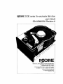
R,9DIME 200E series 5~ winchester disk drive
user manual
R9DIME 200E series 5~ winchester disk drive
user manual
PiN USM0038 Revision A
~/
VRPDIME
Rodime PLC, Nasmyth Road, Southfield Industrial Estate,
Glenrothes, Fife, KY6 250, Scotland.
Tel: 0592·774704. Telex: 728217
Rodime PLC, 25801 Obrero - Suite 6, Mission Viejo,
CA 92691, Tel: (714) 7703085, Telex: 683466.
oo<vmfftt .nd thoe mlOlmahon h~'ln .. prOC)fltl"v to RodtrN
P L,C. No pitt 0' U"'ln'o,m.110n m.... t. duphC,llC1, r..... .,~ Of'
dltcJoMd ""Imaut tt•• I)fIOf Milt'" COntini of Rodufte P.L.C
Th'l docu",-nt 'I lubltet to c1'I.no- W1lhO\.lt notl(t
TtUI
Copyn",. Rocll"","
Le ..
1983
_ _ _ _ _ _R9DIME
@DIME
The purpose of this manual is to provide the user 'Of the
RQ 200E series disk drive with more technical help and
information than is available in the product and interface
specifications. However it should be emphasised that these
latter documents, PRO-OO33 and INT-0034 a-re definitive.
Rather, this manual gives practical advice on drive usage as
well as engineering background on function and design.
Part A: User Guide introduces the drive in section 1 and lists
controller suppliers. Section 2 gives information on installation
into a system. Powering up the drive, description of fault
codes and assistance in trouble-shooting are given in section 3
while section 4 is devoted to repair and maintenance.
PART A
user guide
1 INTRODUCTION
1.1
1.2
1.3
1.4
1.5
General
Specifications
Connectors
Controllers
Illegal Address Map
2 INSTALLATION
2.1
2.2
2.3
2.4
2.5
2.6
Shipping lock
Step rate
Mounting
Multiple drive configuration
Power requirements
Indicators
3 FAULT FINDING
3.1
3.2
3.3
3.4
3.5
Front panel fault codes
Fault codes at power-up
Fault codes during operation
Fault diagnosis
'TRACKER' exerciser
4.1.
4.2
4.3
4.4
4.5
4.6
Tools
Procedure
Spares holding .
Purchase of spares
Repair services
Return of drives under
warranty.
Part B: Product Description is aimed at providing a technical
introduction to the drive design. Sections 5 to 9 deal with
the mechanical configuration, the function of the electronic
circuitry and features of the mi«ropr~r firmware.
Two appendiCes list patents applied for and a recommendationto controller designe("S·of a write-precompensation scheme.
Further help is readily available from Rodime customer
support engineer~ng and this can be obtained by contacting
either the appropriate Sales Office, or by direct contact with
the main plant in G lenrathes.
Rodimeis dedicated policy is t6 ensure customer satisfaction
with both the product and its service and in order to maintain
this, any suggestion for improvement to this manual or our
service is welcome and should be made directly to me at the
Rodime Plant in Glenrothes.
Rodime - right from the oeginning.
4 REPAIR AND
MAINTENANCE
~.
Malcolm F. Dudson
DIRECTOR OF MARKETING
2
3
@DIME
R9DIME
----------------------------------------------PARTB
product description
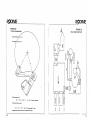
5 MECHANICAL DESIGN 5.1 General
5.2 Rotary aCtuator
5.3 Head/track positioning
accuracy
5.4 Airflow and filters
5:5 Thermal compensation
5.6 D.C. motor and brake
6 MASTER ELECTRONICS
BOARD
6.1 Read data channel
62 Writ~ data interface
6.3 Drive control interface
6.4 Fault detection
6.5 Stepper motor circuitry
6.6 Index
6.7 Links
7 PRE-AMPLIFIER
BOARD
8 MOTOR SPEED
CONTROL BOAFtD
8.1 Drive motor speed control
82 Stepper motor drive circuit
8.3 Brake
8.4 Track zero transducer
9 MICROPROCESSOR
4
9.1 Stepper motor control
92 Protection of index
selection track
list of diagrams
Appendix 1
Appendix 2
Appendix 3
Figure 1
Figure 2
Figure 3
Figure 4
Figure 5
Figure 6
Figure 7
Figure 8
Figure 9
Figure 10
Figure 11
Figure 12
Figure 13
Figure 14
Figure 15
Figure 16
Figure 17
Figure 18
Figure 19
Figure 20
Figure 21
Figure 22
Figure 22
Figure 22
Figure 22
Figure 22
Figure 23
Figure 24
Figure 25
Figure 26
Figur~ 27
Figure 28
Patents
Write. Data pre-compensation scheme
Format recommendations
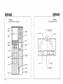
Drive outline showing connector positions
J 1 Connector - control
J2 Connector - data
J3 Connector - power
Control and power bus
Data bus
Mounting details
System with four drives
Wiring of spare hall sensor
Non planar section of RO 204E
Airflow and Filter system
Thermal compensation
Board interconnections
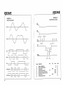
Read channel signals
ReadJWrite data timing
Stepper motor drive configuration
Step pulse timing
Stepper winding switching sequence
Power-up flow chart
Recal ibration flow chart
Write faul, flow chart
(a) Step wait loop
(b) Single track seek and slow mode
(c) Ramped seek modes
(d) Final step roudne
(e) Adaptive settling routine
Master electronics board assembly
Pre-amplifier board assembly
Motor speed control board assembly
(a) - (d) Schematic Master Electronics board
Schematic pre~mplifier board .
Schematic motor speed control board
44
44
45
49
50
50
50
51
52
53
54
55
56
57
58
59
60
61
62
63
64
65
66
67
68
'69
70
71
72
7~
74
75
76-79
80
81
5
R9DIME
@DIME
1. INTRODUCTION
1.1 General
---------------------------------------------------------------------
PART A
occur. flashes the corresponding fault code on a red LED
indicator on the front panel.
user guide
A significant feature of the RO 200E·series is that boards are
interchangeable without the use of oscilloscopes or other
setting up equipment. This js made possible by the fact that
there are no select-on-test components and no adjustments on
the boards whatsoever. This, of course, in addition gives added
reliability which is further emphasised by the fact that there
are no mechanical adjustments.
The Rodime RO 200E series of 5% inches (130mm)
Winchester disk drives provides fast ·access data storage for use
with small business computers, terminals and microprocessor
based systems. There are four models in the series, RO 201 E,
RO 202E. RO 203E and RO 204E containing 1.2.3 and 4
magnetic disks respectively and ranging in total data storage
from 13 to 53 Megabytes. The drive outline is shown in
figure 1.
The drive is a microprocessor based devic.:e which receives
and transmits MFM (modified frequency modulation) data,
seeking the appropriate track in response.to step commands
across the disk control interface. The drive is soft sectored
and is connected to the host system via a disk controller which •
is responsible for formatting. MFM encode and deCode to
NRZ. block address decode. CRC generation and verification
and so on. Typical format schemes with 256 data bytes per
sector and 32 sectors per track can realise an efficiency of
about 80% giving formatted capacities up to about 42 MS.
Dimensions. mounting details and voltage requirements
(DC voltage only) are the same as stand.ard 5% inches floppy
- disk drives. The ~icroprocessor is responsible for the control
of the stepper motor used for head positioning. Fast seek
times are achieved by means of programmed velocity profiles
and microstepped velocity feedback damping routines.
Automatic thermal compensation has been designed into the
head positioning mechanism. A brake is provided as standard
for the main DC disk motor and this permits shipment of the
Rodime drive in a terminal or system provided it has been
mounted in accordance with the correct procedure (see
section 2). A further solenoid brake for the actuator can be
supplied as an OPtional extra. The microprocessor also
monitors certain fault conditions in the drive and shoulq one
6
Several engineering features are subject to patent application
and these are listed in Appendix 1.
Full specifications of the RO 200E series disk drive are given
in two documents:PRO-OO33 (Product specification)
INT-0034 (Interface specification)
1.2 Specifications
A summary of the important performance parameters is given
below:Product specifications
Mode!s:
RO 201 E, 202E, 203E, 204E,
Disks
: 1,2.3.4
Heads
: 2.4.6.8
Unformatted capacity (M bytes) : 13.33,26.66,40.00.53.33
Formatted capacity (typical)
Per drive (M bytes)
Per track (bytes)
Per sector (bytes)
Sectors per track
Cylinders
: 640
Transfer rate (M bits/s)
:5
: 10..49,20.97,31.45,41.94
: 8192
: 256
:32
Seele times (ms) (including settling)
Track to track
:8
Average
:55
: 130
Maximum
7
_ _ _ _ _ _R9D1ME
R9DIM§
Average latency ems)
: 8.3
Flux reversals per inch (max)
: 10.200
Tracks per Inch
: soo
Rotational speed (r -p.m.)
: 3600
Power requirements (DC only)
(see para 2.5)
: 5V (±5%) at 0.6SA typical
: 12V (±5%) at 2A typical
(10%,4A motor start)
Dimensions (inches)
8.00 x 5.75 x 3.25
Operating environment
lcrCto sooC
_'O%RH to 85%RH
(non-condensing)
Vibration
Operating
Non-operating
.006 inch displ.. !H)() Hz
19 pk aceln., 60-500 Hz
: .040 inch displ.. 5-30 Hz
29 pic aceln., 30-500 Hz
Shock
Operating and non-operating
(without transit lock)
Non-operating
(with transit lock)
Interface
: 3g pk. less than 1Oms,
max 2 per second.
: 30g pic. less than 10 ms.
max 1 per 10 second
: ST506 variant of SA1000
(see section 1.3 and 1.4)
1.3 Connecton The RO 200E drive interfaces to host systems via the ST506
interface which has become an accepted standard for 5% inch
Winchester disk dr.ives. There are separate connectors for data
(in MFM code). for control lines and for DC power. The
connector positions are shown iog Figure 1 and the connectors
themselves are defined in Figures 2. 3. and 4. The corresponding
control. power and data interfaces are given in Figures 5 and 6.
A chassis ground tab is also provided. The convention for
control is that a TTL logical zeros is true and a TTL logical one
8
is false. Up to four drives may be connected to a host system
and each drive is provided with a four·hole switch for selection.
The control lines may be daisy-chained but the data lines must
be radially (individually) connected to the host (see section
2).
.
Control signals for the drive are provided via a 34 pin edge
connector (Pl/Jl). The pins are numbered 1 through 34 with
the even pins located on the solder side of the board. Pin 2
is located on the end of the board connector cloSest to
the DC power connector and is labelled. A key slot is pro'lided
between pins 4 and 6. The recommended mating connector
is AMP ribbon connector AlN 88373-3.
Radial connection of read/write data signals is provided via a
20 pin edge connector (P2I42). The pins are numbered 1 .•
through 20 with the even pins located on the solder $ide of
the board. The recommended mating connector is AMP
ribbon connector AlN 88373-6.
DC power is provided by a 4 pin AMP Mate-N·Lok connector
(P3/J3) PIN 350211·1 mounted on the component side of the
board. The recommended mating connector is AMP PIN
1-480424-0 utilising AMP pins PIN 350078-4.
A ground connection is provided via a "Faston" connector
AMP PIN
on the chassis
. 61664·1 located on a metal stand-off
.
between the power and control signal connectors. However,
·the D~ and chassis grounds are common on the drive and the
use of the "Faston" connector is not essential. Wiring should
be in accordance with Figure 5. The frame ground of the host
system should be properly earthed.
The following 5% inch Winchester Dislc Controllers are known
to operate with the RO 200E series disk drive. In general,
any controller which will operate with the RO 100 and RO
200 series disk drives will a_Iso operate with the RO 200E
series disk drive. However. the controller must be able to
address up to 640 cylinders and set the STEP interval in the
1.4 Controllers
9
_ _ _ _ _ _ _R9DIME
@DIME
range 5 ps to 5 ms. Further information is available from the
Rodime Marketing Department or from the controller
manufacturers themselves ..
The stepper motor shipping lock is a label fixed to the top
cover of the drive and covering a plastic pulley on the stepper
motor shaft. thus preventing movement of the read/write
heads across the disk surfaces.
Xebec
S1410
: Microcomputer Systems Corp. PO Box 512.
432 Lakeside Drive. Sunnyvale.
California 94086 (408) 7734200, (408) 7351340.
This label must be removed prior to power-on.
Western
Digital
WD 1000
: Western Digital Corp, Newport Beach, California
9266 (714) 5573550.
1.5 Illegal Address Map
: Konan Corp, 1448N 27th Avenue, Phoenix,
Arizona 85009 (800) 5284563
Each drive is accompanied by a map indicating the addresses of
sectors which should not be used. This map (label) is fixed to
the base casting wall. These illegal sectors have been identified
during unit test in the factory and contain a repeatable disk
defect, greater than one bit in length. NO such illegal address
will exist in cylinders 0, 1 and 2.
An illegal address is specified by cylinder, head and sector. It
should be noted that the format used for this purpose is 33
sectors of 256 bytes each. The.maximum number of illegal
addresses is:-
Model Number
Max number of illegal addresses
10
Warning: Once the label is removed the stepper motor .shaft
should never be rotated by hand since this could lead to headl
disk damage:
Note: This label is not present on units which are fitted with
the automatic stepper motor lock. This lock also releases on
application of 12V.
DTC 510, : Data Technology Corp, 2775 Northwestern
Parkway, Santa Clara. California (408) 4960434.
DTC 520
Konan David
Junior
2. INSTALLATION
2.1 Shipping lock
201 E 202E 203E 204E
4
8
12
16
The drive can accept step pulse intervals over a range from
5 ps to 5 ms. If the interv~1 is in the range 5ps to 130 ps,'
toen the drive is operated in the ramped seek mode. The seek
operation will begin if 32 step pulses have been received or
180 ps has elapsed since the last step pulse was received. In
this mode of operation, the access times will vary with step
interVal. The access times quoted in paragraph 1.2 are for a
step interval of lOps. If the step interval is in the range 130 ps
to 5 ms, then the drive s!ep rate will vary with step interval.
Consequently. the access times are not specified.
22 Step rate
Side brackets with tapped holes are provided with each drive
and permit base or side mounting, -see Figure 7. These
brackets are fixed to the drive chassis via shock-absorbing
grommets. The drive may be oriented in any axis. When
installing into an enclosure at least 0.1 inch clearance must
be maintained around the entire drive to allow vibration
isolation and to prevent obstruction of the breather filter
and the creation of ground loops.
2.3 Mounting
Up to four drives may be connected to one host in.a "daisy·
chain" fashion. A 4-pole drive select switch is fixed to each
drive, (See Figure 1). To identify a drive as number 1, close
th~ first pole of this switch nearest the terminator pack.
2.4 Multiple drive
configuration
11
R9DIME
@OIME
----------------------------------------------Similarly for drives 2, 3 and 4. Only one pole should be in
. the closed position. All "daisy-chained" drives should have the
line terminator pack removed except for the last drive in the
. chRin. All drives are supplied for single usage, that is. pole 1
is closed and the terminator pack is present. (See Figure 1).
Note that, in the multiple drive configuration all data interface
lines are radially connected to the host. Figure S shows a four
drive configuration.
2.5 Power requiremenu
The drive requires DC voltages only.
CURRENT
VOLTAGE
Typ
Max
+5V±S%·
O.6SA
O.7SA
+12V± S%
2.0A
2.4A
In operation, the maximum rate of change of the 12V load
due to the disk drive is SA/ms.
Two red LED's fixed to the master electronics board are
visible through the facia when they are illuminated.
2.6.1.
The "Power-On" LED is on when the drive
is READY with no error condition present. It is
also used to indicate fault conditions in the drive.
2.6.2.
The "Select" LEO is on when the drive is selected
by the host provided the "Power-On" LED is on.
-
Peak During Power-up
4A
No damage will result if power is applied or removed in any
order. However. to avoid tripping the fault detection circuitry
two conditions must be met:
2.S.1.
5V risetime must not exceed 1 second.
2.S.2.
12V must follow the 5V within 5 seconds if the SV
is applied first.
2.S.3.
When checking the power supplies, the following
loads should be used:
For the 12V supply, the power-up current may be measured
using. a standard load of 3 ohms in series with 1 mH and the
operating current may be measured using S ohms in series wi~b
,.,
1 mHo With a 7 ohm resistive load on the 5V supply and the
above loads on the 12V supply, noise and ripple should
not exceed 100 mV peak to peak up to 560 Hz and 50 mV
peak to ·peak from 500 Hz to 5 MHz.
2.6 Indicators
The "Power-Orr" LED is positioned closest to the centre of
the facia. Note that this LED will not come on if the condition
2.5.1. 5V risetime, is not met since the microprocessor will not
receive an initial reset.
The "Power-On" LED is used to flash error messages should
certain fault conditions arise on the drive. A four bit binary
code is used (long flash = logical 1 , short flash IZI9Qica1 0)
with the most significant bit occuring first:
3. FAULT FINDING
3.1 Front panel fault
codes
e.g. short, short, long, short ... 2 (0010)
Fault Code 1 (0001)
No index track data burst.
Fault Code 2 (0010)
No Flag zero
Fault Code 3 (0011)
Motor speed outside ±1 %
tolerance at end of power-up
sequence.
:1111'_------
~D'ME
_ _ _ _@DIME
Fault Code 4 (0100)
. : Motor speed outside ±10%
tolerance in normal operation.
Fault Code 5 (0101)
: Flag zero stays TRUE.
Fault Code 6 (0110)
: STEP received while WRITE
GATE is TRUE.
Fault Code 7 (0111)
WRITE FAULT.
Fault Code 8 (1000)
Not used.
Fault Code 9 (1001)
Not used.
Fault Code 10 (1010)
No index.
Fault Code 11 (1011)
Motor not up to speed.
Fault codes 1, 2~ 3.5, 10 and 11 are monitored during the
initial power-up sequence of the drive. The remaining codes,
namely 4, 6 and 7 are constantly monitored during normal
operation. All fault codes are latched by the processor and the
d rive must be restarted to clear. Codes 3,4, 10 and 11 generate
an interface WRITE FAULT as do those fault conditions
leading to code 7.
32 Fault codes at
power-up
From power-on to drive READY the microprocessor performs
a number of checks and calibrations on the drive. Should any
of these checks fail the drive will not come READY and the
microprocessor will flash the appropriate fault code on the
front panel. The power-up routine is shown in Figure 19.
3.2.1. Codes 10, 11. The microprocessor checks for an INDEX
pul~e (Hall sensor output) from the DC motor. If this does not
occur during a period of 8 seconds, then fault code 10 is
displayed. Since this condition is likely to be the result of the
DC motor not starting, the microprocessor attempts to reduce
head/disk static friction during the period of 8 seconds by
moving the positioner.14
Note that a WRITE FAULT condition removes power from
the DC motor thus preventing thermal damage.
The DC motor speed is then checked to with in ±1% of
3600 rpm. Each check takes one motor revolution and during
this time the pOlNer-on LED is flashed at intervals of
approximately 0.5 second. If the processor does not see 4
consecutive speed samples correct to ± 1% with in 25 seconds
it will display fault code 11.
322. Codes 5,2. When the speed check is successfully
completed, WRITE FAULT interrupts are enabled. The
microprocessor then begins the recalibration of the actua~6r
to track zero. The exact routine is shown in Figure 20. Two
_ possible fault codes may occur. If flag zero does not go
false within 25 steps towards the centre of the disk, tautt
code 5 will be displayed. After going false, if flag zero cannot
then be set true within 800 steps in the out direction. fault
code 2 is displayed.
32.3. Codes 1,3. After calibrating the actuator to track zero,
the processor initiates the routine for selecting the correct
INDEX pulse (see section 6.6 for an explanation of INDEX).
The actuator is moved to track -2 to find the index data burst
on head (/J and so select the corresponding Hall sensor phase,
thus establishing INDEX. Failure to complete this operation,
results in fault code 1- provided link A is present and is ignored
if link A is cut. The actuator is then re-positioned on track
zero and a final check made on the DC motor speed, again to
±1%. Should this fail, fault code 3 is displayed. :
At the successful completion of the power-up routine.
READY and TRACK ZERO are both set true and the head
selects are enabled.
15
_ _ _ _ _ _ _RODIME
R9DIME,
3.3 Fault cod~ during
operation
During normal operation of the drive. fault codes 4, 6 and 7
may be displayed.
3.3.1. Codes 4._6. While the processor is waiting for a step
pulse from the interface it continuously monitors the DC
motor speed. Should the speed vary from nominal by more
than +10% or -5%. fault code 4 will be displayed. The
processor will not allow a step pulse to· be received while
WRITE GATE is true. This is considered to be a catastrophic
controller fault. The drive returns WRITE FAULT status
and displays fault code 6.
3.32. Code 7: WRITE FAULT. On receipt of a WRITE
FAULT interrupt from the drive's hardware detection
circuitry the processor latches this co,"!dition, delays for "2
seconds a~d samples the hardware input to check if the
WR ITE FAU LT condition still exists. If it does~ fault code 7
is displayed. If not, the processor-enters the power-up routine
thus setting the actuator to track zero. See Figure 21.
In the above sense, fault code 7 represents a static WR ITE
FAU LT status. There are nine fault conditions which cause.
WRITE FAULT to be true. One is defined above in 3.3.1.
These are related to read/write heads, "namely:
• no write current in any head when WR ITE GATE and
DRIVE SELECTED are both true
• more than one head selected
• no write data transitions when WRITE GATE is true
One relates to the DC supply, namely:
• 12V supply lower than about 10.0V
The remaining four are abnormal motor conditions as detailed
by fault codes 3.4, 10 and 11.
16
In practice, it is likely that the vast majority of WRITE
FAULT conditions are caused by power supply transients.
Thus. the 2 second ~elay and re-check allows a fast transient
to be recognised but the condition is nC?t latched if the recheck is successful. The controller will receive TRACK ZERO
and READY status and can repeat the command which had
to be interrupted.
A table showing likely causes of the fault codes is given
below. The simplest action to take is that of replacing either
the master board or the motor speed board and verifying
if the fault code persists. However, a set of diagnostic routines
is presented which determine more accurately the cause of.
each fault code" A voltmeter- or oscilloscope and the
"TRACKER" exerciser (see section 3.5) are needed for
this investigation. The causes of fault conditions other than
those given by the fault codes may be more difficult to trace.
In practice. the most likely sources of trouble are (a) power
supplies not meeting specification and (b) step rates outside
the drive constraints (section 9.1). This presumes that the host
controller meets the requirements of the Rodime interface
specification INT -0034.
3.4 Fault diagnosis
In any event, it should be verified that the shipping label is
removed, the connec.tors are clean and properly attached,
the interface terminator is present or absent according to the
configuration. the drive chassis is clear of any system
metalwork. the DC power lines are short twisted pairs and data
and control cables are preferably shielded and do not run
close to high current switching circuits.
-'
3.4.1. For each fault code a possible cause is indicated in the
Fault Table by a letter. This is used in the Diagnostics Table for
idenfification.
17
@DIME-
R9DIME
--------------------------------------------------
Fault Table
t=ault
Code
1
Possible Causes
Action
A: Faulty flag zero
Contact service
organisation
Replace master
board
Contact service
organisation or
replace pre-amp
board
Rewrite with
"TRACKER"
B.
C:
position
Fault in data burst
detection circuitry
Fault in head f/J or
pre-amp board
D: Data burst erased
Fault
Code
3.4.
10,11
Possible Causes
Action
N: Brake failure
P: No 12V supply
Replace
Check supply /
connector
Contact service
organisation
Replace
Faulty DC motor/
Hall element
R: Faulty motor speed
board
Q:
6
S:
T:
2,5
E:
Transit lock label
not removed/faulty
stepper lock option
(if fitted)
F: Connector fault
between motor speed
board and stepper
motor/flag zero
assembly
G: Short circuit between
motor speed board and
casting
H: Faulty flag lero
transducer
J: Fault in stepper
motor control circuitry
K: Fault in stepper
motor control circuitry
l: Faulty stepper
motor
M: Defective positioner
assembly
18
Remove label/chec k
stepper lock soleno id
7
Controller/Interface
fault
Faulty master board
Faulty master board
Fa~lty pre-amp board
W: 5V and/or 12V
too low
U:
V:
Check connector
and/or replace
motor speed board
Reassemble board
I
Contact service
organisation
Replace master
board
Replace motor
speed board
Contact service
organisation
Contact service
organisation
Check controller/
connector
Replace
Replace
Replace
_ Check supply
3.4.2 A numbered set of checks is given for each fault code
displayed on the front panel. The action after each test is
indicated by a number or a letter. The number refers to
another check. normally the next. shown for that fault code in
this table. The letter refers to the determined cause as given in
the previous table.
Diagnostics Table
Fault
Code
1
Test is faulty?
Procedure
1.
Cut link A to let drive JI!C.OlTlt!
ready.
Yes
No
2
19
@DIME
R9DIME
Fault
Code
Procedure
2.
II
3.
I
I
2,5
3.4
10,11
20
4.
Use "TRACKER" to check on
1C9/14 that flag zero Switches
between tracks 2 and 5.
Use "TRACKER" to re-write
date bursts, replace link and
retest.
Replace master board, rewrite data bursts and retest.
Test is faulty?
Yes
No
Fault
Code
4.
A
4
0
e
B
7
1.
2~
3.
Check brake operation.
Check 12V supply.
Change link on motor speed
board to use spare Hall
element.
1.
1.
2.
1.
Check if transit lock label is
rf!moved./Check stepper lock
Solenoid (if fitted).
2. Remove connector J8 from
motor speed board and check
for 14 ohm between J8/6 and
J8n, J8/8 and J819.
3. Check J8 crimp joints.
4. Check for diode between
J8/l1 and J8110.
5. Check J8 crimp joints.
6. Check beneath motor speed
board for shorts to casting.
7. Replace-master board and
retest.
8. Replace motor speed board
and retest.
E
3
Check interface cables/
controller.
Test 12V to be in range 11.4V
to 12.6V. Test 5Vto be in range
4.75V to 5.25V.
Replace master board and
retest.
2
4
F
5
Replace motor speed board
and retest.
3
6
F
6
H
G
7
8
J
M
K
2
P
3
N
3
Q
Test is faulty?
,No
Yes
Procedure
I
Q
1
I
R
S
T
W
2
V
U
Rodime has developed a hand-held exerciser, the "TRACKE R"
which simulates a host controller and allows the user to
exercise any 5% nch Winchester disk drive which operates
via the ST 506 interface. !t is a useful tool for checking a
drive ~ich is believed defective or which has been repaired.
The "TRACKER" comes complete with interface connectors
for data and control and with a 5V supply connector. It
basically comprises a keypad for parameter and instruction
input and six LED's for response.
3.5 'TRACKER' exerciser
It will perform the following commands:
•
Recalibrate.
• Seek track (b to 1023.
• Select head (b to 7.
• Continuous seek between two tracks.
Key selectable step rate (30 us to 25 ms in lOO'us
increments) .
Seek demonstration routine (random, planet satellite).
• Write pattern select (1 F, 2F , DB Hex).
• Write/erase for one revolution.
•
•
21
_ _ _ _ _ _ _R9DfME
R9QIME
• Write/erase for one surface (head).
Disconnect the flat cable connector from the motor speed
•
•
board.
Continuous write.
Check index track . -2.
This device would typically be used with an oscilloscope
and allows actuator and head/media verification. for example.
It may be purchased direct from Rodime. and customers
wishing to do so should contact the plant in Glenrothes or
the appropriate Sales Office.
Reassemble the replacement board in the reverse order
ensuring that the pre-amp connector mates correctly with the
pre-amp board, and the flat cable connector is correctly
polarised.
4.2.2 Brake replacement (time 10 minutes). Remove the
master board as described in 4.2.1 but do not disconnect
the flat cable from the motor speed board. Disconnect the
brake connector from the motor speed board.
4. REPAIR AND
There is no preventative maintenance and there are no
MAINTENANCE
adjustments on the drive. Field repair is restricted to brake
and board replacement and selection of the spare Hall sensor.
Repair to the module can only be effected by use of Rodime
special tooling and Class 100 clean room conditions.
USERS ARE REMINDED THAT REMOVAL OF THE
Remove the two screws securing the brake to the casting
using the number Pozidriv screwdriver, and remove brake .•
MODULE COVERS WILL RENDER WARRANTY VOID.
Place the .015 inch feeler gauge between the motor rotor and
the brake pad and push the brake body such that the
plunger fully depresses against its spring. Ensure that the
centre line of the brake lines up with the motor centre and
4.1 Tools
The tools required for field repair consist of:
•
Supadriv screwdriver, number 1 •
• . Pozidriv screwdriver, number 2.
4.2 Procedure
•
•
Box spanner, ~ inch AF.
Hex driver (Allen) 5/64 inch.
•
•
.015 inch feeler gauge.
"TRACKER" exerciser (Optional).
Access to the brake, pre-amplifier board and motor speed
board is achieved firstly by removing the facia, then the
master board and finally the side brackets.
Position the replacement brake and refit the screws loosely.
-
lock the screws. Reconnect the brake connector.
Reconnect the power connector ensuring correct
polarisation..
Power up the drive with the master board lying alongside
and check that the brake does not contact the motor rotor.
Power off and check that the stopping time is in the range
5 to 8 seconds.
4.2.1 Master board replacement (time 5 minutes)'
22
Using number 1 Supadriv, remove 4 screws holding facia
Refit the master board as described in 4.2.1.
and remove from drive. Using 5/64 inch Allen key remove
the'five (5) screws securing the board to the drive, and
carefully lift the board free of the drive.
4.2.3 Motor speed board replacement (time 10 minutes).
Remove the master board as described in 4.2.1.
23
@DfME
R9DIME
..........------------..........---------------------------Remove the three screws and stand-off securing the
mounting brackets to the casting and carefully remove the
side brackets.
Disconnect the brake, DC motor and stepper motor from the
motor speed board.
Complete the reassembly as described in 4.2.3.
42.5 Verification. The Rodime hand-held ".TRACKER"
exerciser is a useful tool for verification of a repaired drive
prior to final systems use. This device is more fully described
in Section 3.5.
Unscrew the rear stand-off and remove the motor speed board.
If the spare Hall element is to be connected this is achieved by
removing the link on the motor speed board and reconnecting
it as shown in Figure 9.
Reassemble the motor speed board in the reverse order
ensuring correct polarisation of connectors, check that the
ground contact is correctly positioned between the motor
speed board and the casting.
42.4 Pre-amplifier board replacement (time 30 minutes).
Remove the master board and side brackets as described
in 42.1. and 4.2.3.
Desolder the flexible cables from the pre-amp board using
solder wick and a fine tipped solder.ing bolt (maximum
temperature 3Oa'C). Care must be taken to minimise the
heating of the flexible cables.
Remove the two (2) screws securing the pre-amplifier board tCl
the casting and remove the pre-amp board.
24
4.3 Spares holding.
It should be emphasised that the following figures are
recommendations only and that it will be up to each
individual customer to decide upon the appropriate spares
holding.
Description
Drives on site
Part No.
1-99
Master board assembly
Speed board assembly
Pre-amp board assembly
Failsafe brake assembly
ASY5118
ASY5083
ASY5116
ASY2072
100-250
2
1
1
>250
5
2
1
2
Other spare parts such as bracket/facia assemblies, terminator
packs, ground tabs and consumable items such as warning
labels are also available.
Spare parts for use as a customer spares holding may be
purchased directly from Rodime or from Rodime appointed
distributors.
Fit the replacement board to the casting using three (3) nylon
washers behind each screw position.
Spares may also be purchased on an exchange basis under
which Rodime will supply a new or refurbished sub-assembly
making a financial allowance on the returned unit.
Place the flexible cables over the pins on the board and solder
using a fine tipped bolt.
Price lists may be obtained from Rodime, its sales offi~ or
authorised distributors.
4.4 Purchase of spares
@DIME
45 Repair services
_ _ _ _ _ _R9DIME
Rodime operates a repair service under which drives will be
repaired for a standard service charge.
For drives which are out of warranty when this service is
required, Rodime should be informed in writing of the
suspected defect. If the drive is to be returned, a Return
Authorisation. number will be given.The drive should be
packaged in the original shipping container and returned to
Rodime or to the distributor from which the drive was
purchased together with a full description of the fault
condition.
If the original packaging has been mislaid, a suitable container
may be purchased from Rodime or the distributor. _
Rodime cannot assume any responsibility for damage incurred
to the drive during the shipment and insurance is the
responsibility of the customer.
In the event of other problems Rodime, or the
appropriate distributor, should be informed in writing
of the suspected defect. If the drive is required to be
returned a Return Authorisation Number will. be given
and the drive should be returned pra.paid. The same
procedure as in 4.5 above applies.
If on examination the drive is proved defective under
terms of the warranty, the drive will be repaired or
replaced, at Rodime's sole discretion and returned to the
customer at no charge. If the defect is found to be due
to mis·handling or other causes, the drive will be treated
as a standard repair and charged accordingly. If, on
examination, no fault is found, the drive will be returned
at the customer's expense. RO.dime reserve the right to
make a charge for testing and handling under these
circumstances.
Rodime will return the goods carriage collect and a charge
will be made for any shipping container which Rodime may
have to provide.
Further details of this service may be obtained from Rodime
or its authorised distributors.
4.6 Return of drives
under warranty
Rodime Terms and Conditions of Trade include a
warranty for a period of twelve months from date of
shipment. The procedure for return of drives under
warranty is as follows:·
If the drive fails within the first five days of operation
please. contact immediately the Marketing Department
at Rodime or the distributor from whom the drive was
purchased.
26
27
R9PIME
NOTES
_ _ _ _ _ _ _R9DIME
PARTB
product description
The important perfor~ance and reliability aspects of the
RD 200E disk drive mechanical design may be summarised as.
follows:•
•
•
•
•
•
- •
•
•
•
5. MECHANICAL
DESIGN
5.1 General
Up to four disks in "mini·floppy" size compatible unit.
Designed for easy assembly of heads and disks.
Minimum number of components to maximise reliability.
Two chamber principle with heads/media in one and
actuator mechanisms in the other.
Low inertia positioner for reliability and fast access.
Geometry designed to· minimise head yaw.
Drive components designed to compensate for thermal
head/disk movement.
DC brushless motor with ferrofluidic seal and integral
ventilated hub.
Breather filter positioned to equalise pressure across DC
motor bearing.
Air flow designed to locate drive components upstream
from re-circulating filter and downstream from heads!
media thereby creating an optimum purge cycle.
The positioning systE.'fT1 consists of a stepper motor which
drives a tensioned steel band via a pulley. The band in turn
moves a drive arm which is attached to a shaft. The shah:
rotates in a bearing system and moves the head arms across
the disk. Simplicity of components ensures easy assembly
and reduces failure risk.
5.2 Rotary
actuato~
The tvvo phase stepper motor operates in a fractional-step
mode under microprocessor control (0.45° per track).
5.2.1 Stepper Load. The pos~tioner has low inertia to provide
28
29
_ _ _ _ _ _ _R9DIME
R9DIME
fast seek times (maximum velocity 7000 tracks per second)
from the available stepper motor power.
5.2.2 Yaw. The geometry ·of the positioning system restricts
head yaw to a range of only aO. The distribution of this angle
is chosen such that the ratio of yaw angle to linear disk speed
is approximately the same at outermost and innermost tracks.
5.2.3 Bearings. The actuator system utilises two half-shielded
rleep groove ABEC 3 ball bearings arranged in a back-to-back
configuration with a dimensional axial preload of 51bf for
optimum stiffness.
5.2.4 Band. The drive band geometry is designed to give
symmetry of movement and to minimise band radii and
flexin~ angles. The band is etched from stainless steel with a
typical tensile strength of 250K psi. There is a safety factor
of approximately 40 between the breaking stress of the
band and the dynamic peak tension.
End stops restrict over-travel should contr91 be lost and
will prevent readlwrite heads from either striking the disk
hub or coming off the disk.
- 52_5. Flag zero. Track zero is defined from a combination
of a particular stepper motor phase (one of eight) and a
flag mounted on the drive arm. This flag is set up, using
a .special assembly fixture to switch on opto-interrupter
(track zero transducer) mounted on the base casting. The
flag is set to sWitch between tracks 3 and 4. Track zero
requires the flag to be true (transducer interrupted)
and the correct stepper phase to be selected. Note that
the opto-interrupter and drive components are in the
sealed lower chamber and hence protected from
contamination and accidental handling damage.
30
The requirements of the positioning system are (a) that
tracks do not touch and (b)" that an acceptable signal to
noise ratio is obtained when the same track is
overwritten. Broadly speaking, the first condition
determines the maximum track pitch error. In the case
of the RD 200E drive it relates mainly to the static stepper
motor accuracy. The second condition relates to the
repeatability of the positioning system. Thus given a
specification for the repeatability tolerance the required mean
(static) step accuracy of the motor can be determined for
a given track density.
5.3 Head/track positioning
accuracy
The airflow generated by disk rotation causes air to flow
from the disk chamber through an aperture into the drive,
chamber and to return via it recirculating filter. This flow
system ensures equalisation of temperature during warm
up·by moving air over all components. By positioning the
recirculating filter upstream from the heads and the
drive components downstream from the heads optimum
purge conditions can be achieved. The disk hub is
designed to ventilate the inter disk spaces from both ends
thus ensuring adequate air flow across the disks.
5.4 Airflow and filters
The breather filter situated on the top cover is positioned
on the disk rotational axis. This compensates for
atmospheric changes and maintains a pressure balanceacross the DC motor. bearings reducing the risk of ingress
of contaminants. The breather filter is 99.97% efficient to
0.5 urn particles and the time taken to equalise pressure
is less than one second.
The r~irculating filter is positioned in the drive cham~r
upstream from the disk chamber. This ensures that any
particles generated by moving parts are retained by the
filter and prevented from contaminating the disk
chamber. The recirculating filter is 99% efficient to 0.5
um particles giving a purge time of 12 seconds.
31
_ _ _ _ _ _--=-R9DIME
R9DIME
5.5 ,~herrnal comperisation
The positioning mechanism is designed to compensate
automatically for head to track mispositioning caused by
thermal effects. The thermal loop in the disk chamber (motor
hub, disk, head flexure, head· arm. shaft. bearings. bearing
housing and base casting) causes the readlwrite head to move
outwards from track centre as temperature rises. By careful
design of geometry and materials. the thermal loop in the
drive chamber (stepper motor, band. drive arm, shaft, bearings,
bearing housing and base casting) causes a counter rotation
of the actuator thereby maintaining the heads on track
centre. See Figure 12.
The resUlting misposition ;s about 1 uin per 1°C temperature
change~ It is estimated that this would be about S-10 uin
per ·C the absence of this compensation mechanism.
i"
5.6 D.C. motor and brake The motor is a brush less 2-phase external rotor DC motor
with integral hub and commutation effected by Hall sensor.
A spare.Hali sensor is provided in each motor. The motor
uses preloaded ABEC 7 bearings and is balanced in two planes
to better than 0.25 gm cm. A ferrofluidic seal is fitted above
the top bearing. The disk hub is grounded to the master
electronics board via the motor shaft and a button contact.
The brake is a plunger solenoid designed to stop the motor
in 5 seconds and to provide a restraining torque during
handling. The brake pulls in at 12V and holds off at 5V.
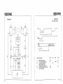
6. MASTER
ELECTRONICS BOARD
The master electronics board layout and schematics are given
in Figures 23 and 26 (a) - (d). This board provides the
following circuit functions:•
•
•
•
•
32
read data channel and interface
write data interface
drive control interface
fault detection
stepper motor control circuit
In addition the master board provides DC power distribution
and control to the motor speed control board and the preamplifier board. The interconnections between the various
boards are illustrated in Figure 13.
Read data from the pre-amplifier board is received differentiallY
on the lines RD+and RO-. The 592 video amplifier,IC1.
amplifies the readback signal by a factor of 20. Components
R7, RS, C6. C7, L1, L2, C53. L5, L6 form a fifth order
low pass Butterworth filter with a characteristic frequency of
4.5 MHz. The second 592, 1C2, is configured asadifferentiator
and transforms the peaks of the readback pulses to zero
crossings which are detected by the zero-crossing detector,
IC3.
6.1 Read data channel
The output signal on 1C3 pin 1 is high when the input signal
is positive and low-when negative. IC3 pin 10 provides a
negative pulse of duration lOOns for every zero-crossing on the
input signal. These two signals are used as the data and clock:
inputs to the D·type flip·flop, 1C4. This connection provides
a time domain filter which will reject zero-crossings occuring
at less than 100 ns intervals.
The exclusive-or gate le5 generates a pulse for every edge
output from IC4 pin 5 using the delay generated by the series
connection through the elements of IC6 and IC7.
The signals ±MFM READ DATA are transmitted to the host
for decode.
Figure 14 illustrates a typical read back signal at various stages
in the read channel. Figure 15 shows read/write data timings.
Write data from the host is received on the lines ±MFM
WR ITE DATA. This differential signal is transmitted to the
pre-amplifier board as the single ended signal WDI using.the
line receiver IC7.
6.2 Write data interface
33
_ _ _ _ _ _ _R9DIME
R9QIME
The signal WRITE GATE from the host is inverted and
transmitted to the pre-amplifier board as RNI.
Precompensation of write data is recommended and a
preferred scheme is shown in Appendix 2. The compensation
applies to the centre bit of .each five bit pattern. The amount
of compensation should be 10 to 12 ns and it is recommended
it be applied to all cylinders.
6.3 Drive control
interface
All input lines on the control interface are terminated by a
220 ohm resistor to +5V, and a 330 ohm resistor to logic
ground. The input line receivers and output line drivers are
74LS244 buffers with tri-state outputs.
6.3.1.lnput'lines. WRITE GATE and HEAD SELECT (/),
1,2, are hard wired to their appropriate circuits on the master
electronics boards. DIRECTION iN and STEP are connected
to input pins on the 8049 microprocessor. since th~ control
of the stepper motor is achieved totally through firmware.
6.3.2. Output lines. SEEK COMPLETE. TRACK ZERO and
READY are generated by the 8049 microprocessor. INDEX is
derived by dividing the output from a Hall sensor on the drive
motor by 2, since two pulses occur per revolution of the
motor. The width of the output pulse is set to approximately
- 200 ps before tran~mission. WRITE FAULT is set true if any
of the drive fault conditions occur, as described in section 3.3.
DRIVE SELECTED is set true if the DRIVE SELECT signal
from the host corresponds with the drive select switch setting
on pg, and if the drive is READY.
6.4 Fault detection
34
Two modes of fault detection are used in the drive. One is
implemented in the microprocessor firmware and is described
in section 3. The other, which is implemented in hardware, is
described in this section. Three drive faults are detected.
6.4.1. Write Unsafe (WUS). This signal is transmitted from the
pre-amplifier board and is gated through an exclusive 0 R gate
with RrN. It is high when a pre-amplifier write fault has been
detected or when the pre-amplifier is in the read mode.
6.4.2. Low +12V rail. IC9 pin 4 has a 4.3V reference voltage
level established from 03. leg pin 5 monitors the +1 2V rail
and when it drops to 10.0V, leg pin 2 will go low. This
condition is wire 0 R 'ed with the Write Unsafe condition, and
when low. signals a hardware WR IT E FAU LT to the
microprocessor.
6.4.3. Low +5V rail. IC9 pin 13 will go high if the +5V rail is
less than 4.3V. In. this condition, RST will be low which
will hold the microprocessor in a Power-up reset state. Aloo
WCR will be high which will tum off the write current on the
pre-amplifier board.
Stepper motor control is achieved totally by firmware in the
8049 microprocessor. See section 9.1. Eight lines from the
mic~op;'ocessor control the stepper motor drive circuits on the
master electronics board. Figure 16 illustrates the connection
between the microprocessor, the drive circuits and the stepper
motor via the motor speed control board.
6.5 Stepper motor circuitry
Th~ stepper motor has a two phase bipolar winding
configuration and a velocity sensor mounted externally. The
windings are driven by constant current drivers mounted on
the motor speed control board.
The magnitude and direction of current is controlled by the
circuits on the master electronics board. The direction control
is direct from the microprocessor using the signals APH and
BPH. The magnitude can be set at one of two levers, high or
low, and is defined by the singals AVR and BVR. Using these
four signals, an 8 step switching sequence can be obtained as
shown in Figure 18.
35
R9DJME
~DJME
-------------------------------------------------The velocity feedback from the velocity sensor is used for
damping and is picked up from one of two coils depending on
cylinder number (VFA and VFB). It is added or subtracted.
true or inverted. depending on the step in the switching
sequence and direction of travel. This is controlled by four
lines from the microprocessor AFB. AFB/. BFB and BFB/.
The signal VDS defines which velocity sensor coil is used. and
also switches REDUCED WRITE CURRENT (RWC) on the
pre-amplifier board. The transition occurs at cylinder 210.
is only relevant to certain controllers provision has been made
to ignore this fault code. Cutting link A will cause the drive
to ignore the loss ofthe data pattern. Section 9.2 gives details
of features designed to protect track -2 from accidental
overwrite.
There are two user definable links on the master board close to . 6.7 Links
the microprocessor.
Link A. This link is cut to circumvent the fault caused by the
loss of the INDEX calibration track. See section 6.6.
A position settled signal, POK, is derived from a window
comparator monitoring the velocity feedback. and is used by
the microprocessor to determine SEEK COMPLETE.
6.6 Index
INDEX is an interface signal used to mark a fixed reference
point relative to the disk. The Rodime drive does not have a
separate INDEX transducer but instead uses the output of the
Hall sensor inside the DC motor. This sensor output is a square
wave which has a 50% duty cycle and makes 4 transitions in
one disk revolution. This is then divided by two and used to
trigger a monostable which gives a 200 us pulse once per disk
revolution.
This hardware scheme results in a ~on-unique INDEX that is
one of two each 1800 apart. Normally this would not be
significant since INDEX should only be used during a drive
format. However, some controllers require a unique INDEX
for reading.
The following procedure is used to ensure the INDEX is
always unique. A special data pattern is written by head (/)
on one half of track -2 during drive manufacture. At
power-up a comparison is made between the Hall sensor
output and the data burst and a unique index is selected.
If the data burst is not found on track -2. the drive will
'display fault code 1. Since the uniqueness of the INDEX signal
36
Reset link. When this link is inserted. J2 pin 5 is connected to
the RESET pin on the microprocessor. This will allow an
interface RESET if J2 pin 5 is held at less than 0.5V for a •
minimum of 12.5 PS. then returned to 3.8V minimum. Note
that the microprocessor has an internal pull-up of 200 Kohm
on this line.
The pre-amplifier board layout and schematics are shown in
Figures 24 and 27. This board provides a means of connection
for up to eight read/write heads: Two SSI 117 monolothic
integrated read/write circuits provide the following functions:·
•
•
•
•
7. PRE-AMPLIFIER
BOARD
pre-amplification of read data
write amplifiers
head selection
write fault detection
Each circuit can support four read/write heads.
ROX and ROY are the differential read data signal lines to the
master electronics board.
HSO and HSl select 1 of 4 heads on each circuit.
HS2 and HS21 select which circuit is active.
37
@DIME
------------------------------------------R9DIME
.....
WUS is the write unsafe signal which is low when the chip is _
writing normally. The high (unsafe) level will be caused by:(a)
(b)
(c)
(d)
(e)
(f)
(g)
Head input shorted to ground.
Head input shorted to centre tap.
Head inputs shorted together.
Head input open.
Centre tap open.
No write data transistions.
No write current.
(hi 6..ny combination of above.
(i) Chip is in read mode.
Chip is disabied (HS2, HS2/).
m
Certain lines have been mentioned in the text. These are
defined as follows:
•
•
•
•
8. MOTOR SPEED
CONTROL BOARD
The motor speed control board layout and schematic are
given in Figures 25 and 28. This board provides the following
circuit functions:•
•
•
•
8.1 Drive motor speed
control
38
WDI is the WR ITE OATA INPUT line.
R/W is the read/write mode select line.
RWC is the reduced write current line.
WCR is the write current return line which can turn off the
write current.
DC motor speed control.
stepper motor drive circuits.
solenoid brake power supply.
track zero transducer power supply and output
termination.
Speed control of the drive motor is achieved using a phaselocked loop (P.L.L.) technique. The drive motor rotates at
3600 rev/min and generates two feedback pulses per
revolution from an internal Hall effect IC. This results in a
120 Hz feedback signal which is phase-locked to a reference
signal generated from the microprocessor crystal oscillator
on the master electronics board. A speed variation of less
than 0.1 % is achieved.
The Address latch ~nable (A.L.E.) signal from the
microprocessor is used as the reference. This signal (REF
ClK)' frequency 733 KHz, is divided by 6144 using IC1 and
IC2 to give a 120 Hz input to the phase/frequency detector
IC3. The other input to IC3 is the feedback signal from the
motor Hall sensor.
The output signal on IC3 pin 8 is a DC voltage proportional
to the phase difference between the two input signals. R4, R1B,
C2 and IC4 form the electronic compensation network that,
ensures the stability of the control loop. The resultant signal
on IC4 pin 7 drives the motor via the emitter followers' 01
and 02, and the power amplifier Darlington transistors 03
and 04.
A two phase drive motor is \.Ised, and commutation between
the two phases is accomplished using the Hall IC output.
This signal. and its inverse, alternatively enables either 03
or 04, depending upon the phase of the commutation cycle.
The Hall sensor signal is a,lso sent to the master electronics
board, where it is divided by 2 and used as the drive INDEX
signal. A spare Hall sensor output is provided, and in the event
of output failure, the spare may be connected by wire link
selection.
Current in the windings of the stepper motor is controlled
by two constant current drivers IC5 and IC6. The magnitude
of the current is controlled by AVR, SVR, and the direction
by APH, SPH. The stepper windings are connected between
ACA and ACS, SCA and SCS.
82 Stepper motor drive
circuit
39
_-----"R9DIME
R9DfME
The signals AOF and BOF hold the drivers in an off condition
until the spindle motor is up to speed during the power·up
sequence.
8.3 Brake
8.4 Track zero transducer
9. MICROPROCESSOR
Power is supplied to the solenoid brake initially from the
+12V rail until it pulls in and the DC motor is up to speed.
Thereafter, power is supplied from the +5V rail via diode 03
to reduce running power dissipation.
The resistor R18 is a bias resistor for the LED in the opto·
interrupter. A nominal forward current of 30 mA is supplied.
The resistor R17 is a pull-u~ resistor for the photo-tra~$istor
which is connected in the open-collector output configuration.
The microprocessor used in the RO 200E series is a member of
the 8048 family of single chip processors. The particular type
used is the 8749, an EPROM version with 2048 bytes of
internal program merTlory and 128 bytes of RAM. The
microprocessor cycles at 11 MHz. giving an instruction time of
1.36JlS.
The processor has three main functions:,. stepper motor control.
• interface handling.
• track positioning monitoring,.
It also indirectly controls the DC spindle motor since the
733 KHz ALE signal output from the processor is used as a
reference frequency for the P.L.L.
9.1 Stepper motor control
Four interface signals are used to control the stepper motor.
STEP. This input signal is used in conjunction with
DIRECTION IN to move the stepper motor. It is connected
to the 8749 T1 pin. This is a special input to the
microprocessor which is used to clock an internal 10 bit
counter. This counter is reset prior to each seek. Once the
first STEP pulse is received the processor issues stepper motor
phase changes until the number of changes equals the value
in the counter. At this point the seek is terminated and SEEK
COMPLETE is set true after final step damping.
DIRECTION IN. This input is connected directly to an I/O
pin of the processor. It defines the direction of motion of the
stepper motor. Once the first STEP of any seek has been
received the microprocessor samples this input and internally
stores the result. The input is then ignored until the next seek.
seEK CO~PLETE. This status line is driven by a S-R flipflop. STEP resets the flip-flop false. It is set true with an
output from the microprocessor.
TRACK ZERO;This stat~s line is driven directly from the
microprocessor. It will be set true when the read/write heads
are positioned with correct stepper motor phase over track zero, false otherwise.
Velocity feedback is obtained from a tachometer fitted to the
endcap of the stepper motor. This feedback is employed (a)
to assist in the control of the motor whilst is is slowing down
on the final approach to the desired track and (b) to control
the settling when the motor reaches the desired track. This
results in settling time being greatly reduced from that which
could be obtained under open loop conditions.
'
An important additional benefit gained from the use of velocity
feed-back is that the microprocessor can examine a digitised
velocity signal to ensure that the positioner assembly is fully
settled before setting "SEEK COMPLETE" status.
All step pulses are buffered by the microprocessor. Two
factors determine the stepping rate of the head assemb!y.
- the interface step rate.
- the length of the seek.
41
40
@DIME
@DIME
-------------------------------------------------Stepper rate is defined as follows:a)
Input Step Rate 5 J,lS to 130 J,lS.
See~
Length
(N)
N<5
5';; N
< 32
32~N<
150
150~N<639
b)
c)
d)
Stepper Rate
Slow (1 ms)
Moderate accn/decn ramps
Fast accn/moderate decn ramps
Fast accn/fast decn ramps
I nput Step rate 130 J,lS to 900 J,lS.
Stepper rate = 1 ms.
Input Step Rate 900 J,lS to 5 ms.
Stepper rate = variable.
Input step rate greater than 5 ms may cause seek errors.
In the ramped mode of operation the maximum step rate to
which the stepper motor accelerates is 7000 steps/second.
The acceleration/deceleration ramps chosen are based on the
length of seek required. This choice ensures optimum access
times with defined settling performance.
In the ramped seek mode (ie, for input step rates in the range
5 to 130 J,lS) the microprocessor will move the positioner
assembly before all the step pulses have been received in
accordance with the following conditions:-.
a)
More-than 31 step pulses have been received
'Soft' endstop protection is also provided by the
microprocessor. An internal track counter which is
dynamically updated means that the processor is aware of how
close the mechanical assembly is to the mechanical endstops
at any point in a seek. This means that if a seek is requested
to an illegal cylinder number, the microprocessor ramps down
the stepper motor and stops at the last legal cylinder number
attainable in the direction requested (ie, stops at cylinder (/)
if a seek is attempted to a negative track and at cylinder 639
if a Seek to a cylinder> 639 is requested).
This protection operates for all legal step rates in any direction.
In the event of a failure in the velocity damping system.
resulting in an undefined settling performance, tlie
microprocessor will initiate ~ln auto-recal prior to settling seek
complete.
Protection of track -2 is considered to be of prime
importance and a number of safeguards have been built into
the firmware.
9.2 Protection of index
selection track
92.1. All interface controlled seeks beyond track zero are
prohibited by the microprocessor.
At the end of each seek and before SEEK COMPLETE is
issued a check is made. If either of the following conditions
is detected then an auto-recal will be executed.
or
b)
180 J,lS has elapsed since the last step pulse was received
After moving off, and as further step pulses are input. the
microprocessor makes decisions about acceleration and
deceleration on the move. This also ensures that access times
are minimised.
42
(a) Flag zero is detected and the internal track counter is not
at zero.
(b) The track counter is at zero and flag zero is not true.
43
@DIME
@DIME
----------------------------------------------
APPENDIX 1
APPENDIX 3
Format Recommendations
Patents
European
Application
Number
US Application
Number
Title
81305976
332003
"Read-Write Head Thermal
Compensation System ...
82302197
373281
"Method and Apparatus for
Controlling a Stepper Motor."
82303263
391010
"Generation of Unique Index
Mark from the Commutation
of DC Brushless Motor."
I
82303262
391150
"Damping of Stepper Motor
using Non-Active Windings."
388165
'Ventilation System for
Computer Disc Drive Hub
Assembly."
-
APPENDIX 2
Write Data Pre-Compensation Scheme
Data sequence
leftmost bit
written first
1001 0110 I
100101111
, .00 I 1 10 I
/0011111/
I 01 I 1 , 00 ,
I 01 11 01 I
110 I 0 00 1
, 10' 0 / 01 I
I
I 10 I 1 / 10 /
110111111
11111100/
111
01
11 I I
Required write
pre-compensation of
centre bit
EARLY
EARLY
LATE
LATE
EARLY
EARLY
LATE
LATE
LATE
LATE
EARLY
EARLY
I
1.0 The following sections describe the general formatting
recommendations for the RO 200E series disk cirives.
2.0 Encoding. It is recommended that data be written on the
disk using an MFM encode. The algorithm to convert
from NRZ data to MFM data is as follows:·,
For a "1 " write a flux transition in the middle of the
bit cell; for a "0" write a flux transition at the start of
the bit cell except when a "0" follows a "1".
3.0 General Requirements. The format of the data recorded
on the disk is totally a'function of the host controller.
The two most common formats allow 32 x 256 byte
sectors or 16 x 512 byte sectors to be written on each
track. A soft sectored format should be used. The start
of each sector is identified by a unique byte which is
written on the disk. This byte is normally an invalid
MFM code (eg. Hex A 1 with a missing clock bit). This
unique byte is used to flag the start of the sector
address field (containing the physical sector address)
and also to trag the start of the sector data field.
4.0 Sector Format Example. An example of a recommended
format for a 256 byte sector is given in Fi~ure A. A
full description of each item is given below:H
1.
Inter Sector Gap. (15 bytes of Hex "4E
gap to allow for disk speed variations.
2.
Sync Field. (13 bytes of '00"). Provides VFO lock-on
prior to data retrieval. The minimum number of bytes is
dependent on VFO lock up performance of host data
separator.
).
Tolerance
44
45
@DfME
@DfME.
------------------------------------------3.
Address Mark. C1 byte of Hex "A 1" with missing clock).
Identifies beginning of address field.
5.0 Index Gap. The gap at the beginning of index allows
for head switching recovery, so that sequential sectors
may be read without losing a complete disk revolution.
Minimum length is 12 bytes, Hex pattern "4E". Normal
recommendation is 16 byte lengths.
4.
Address Mark. 1.0. Field Identifier (1 byte Hex "FE")
Identifies with previous address mark the beginning
of the address field.
5.
Cylinder Address. (1 byte, "0" to Hex "FF").
The most significant bits in the Head Address field (6)
can be used to represent the most significant bit of the
Cylinder Address.
6.
Head Address. (1 byte. "0" to '7").
6.0 Speed Tolerance Gap. This gap at the end of the last
physical sector (before index) provides a spindle speed
tolerance buffer for the whole track. A full track format
routine begins and ends with detection of index. It is
usually a Hex pattern "4E", and the actual number of
bytes depends on media speed during the format
operation.
7.
Sector Address. (1 byte, "0" to Hex "1 F").
7.0 Sector Interleaving. It is possible to interleave sectors to
S.
Address ECC. (3 bytes). Available for ECC check of the
address field.
9.
Gap. (2 bytes "00"). Allows write turn-on time when
updating the sector data field.
improve data throughput during typical read/write
operations by allowing multiple sector transfer within
a single revolution.
10. Sync Field. (13 bytes of "00"). Provides VFO lock-on
prior to data retrieval.
11 .. Address Mark. (1 byte of Hex "A 1" with missing clock).
Identifies beginning of data field.
12. Address Mark Data Field Identifier (1 byte Hex "FS").
Identifies with previous address mark the beginning of
the data field.
13. Data. (256 bytes of data).
14. Data ECC. (3 bytes). Available for ECC check of the
data field.
15. Gap. (2 bytes of "00"). Allows write turn-off time
when updating the sector data field.
46
47
@DIME
@DfNJE
~--------------.---------------------------
FIGURE 1
Drive outline showing connector positions
~
I
~
..:
<
<
0
If
Q
.
t!
~
!::!
9~
I-
L
= ~~
.,. S
;
;:
I
co
J3~
..:
I
J4 Ground
~~
Line TermiNtion
Resistor Pack.
~
..:
!Za::
Jl Control
0
0
<
l
1#1
nOat.
DrM SeIct Switch
~
!
0
I
!
.,I
48
I
49
R9DIME
R9DIME
-------------------------------------------
I
FIGURE 2
FIGURE 5
Control and power bus
J1 Connector - Control
j
I.
1,.06
'.036:t.OO4
Host SyStem
341
,
2.16
FI.t Ribbon or Twisted
p,ir 20 Fl. M,x.
Nom
I-
.~~.~~~.
~No",~~
.062!
brd Thicknt!SS
.007
I
Reduced Write Current
1.775
2
3
4
5
6
7
Head Select 2
Wrile G,tt
~""------~~-:-:---------t
±
RO 200E
.05 Nom
.01 Nom
Seek Complete
Trxk 000
.01
8
9
10
11
12
13
14
15
16
17
18
19
20
21
22
23
24
25
26
27
28
29
30
31
32
33
Write Fault
Head Select 0
ReServecIlto J2 Pin 71
FIGURE 3
Head Select 1
J2 Connector - Data
-
t- J11P1
Index
..
Reedy
SteP
Oriw Select 1
Driw Select 2
.05 Nom
Drive Select 3
.01 Nom
Drive Select 4
Board Thickness
.062: .007
1.075;1.01
Direction In
,....
+5VOC
X
+5V Return
'-/
FIGURE 4
J3 Connector - Power
...j<-
oe
50
I
,....
+12VOC
X
....,
+12V Return
34
4
3
1
2
"'*"
}
51
R9DfME
@DfME
,--------------------------------------------
FIGURE 7
Mounting details
FIGURE 6
Data bus
8.00 Max.
.\
A - Vented Felli FAC2091
B - PJ.Jn Felli FAC2107
A- .065 t .01
B -.05 t .01
R0200E
Ori\'e Selected
1
2
Resen-ed
3
4
5
6
Reset (OptionalJ
R~
i
-
ltoJl Pin 161
-
7
8
9
10
A-3.38
*.01-
8 -3.35
s .01
~~
Sp.)re
Ground
11
+MFM Write Dag
12
-
'--
.86
j:.02
I
I
-~
-EIT- •
1.87 j:.02
3 25
+ .010
000
,
t
_l.12j:.02
Mounting Holes 6-32 UNC
4
on base
2 on each side.
13
-MFM Write Data
14
Ground
15
3.12 j:.02
1.87 j:02
!
I
I
16
+MFM Read Dag
17
-MFMRudDag
--i="
-
19
20*
-
~ 1'--
-
18
Ground
.125
I
I
j
5.SOj: .02
5.75
t
:t .02
.0 1
9"5.85
toO 1
I
f
52
!
I
~
-H iroA-.D65t.01
B -.05 t .01
-~ ! H - - -
Oimensions in ind1es
53
@DIME
I
@DfME
------------------------------
FIGURE 9
Wiring of spare hall sensor
FIGURE 8
System with 4 drives
,
Control
r
oJ
L
J1
rJ2
l.
Of"", : 1
rJ3
I
J4
L
Y
r
Control'"
L
Jl
rJ2
l.
Or"",: 2
rJ3
1...,
-
J4
I
y
r- J1
L..
r
L.
0...
Secl¥ltOl'
h
f-J
h
f-J
'T
'h
l.
h
54
J4
L.
r
L
OriYe: 3
rJ3
r-'
I
J2
-
J1
r J2
f-J
1-
I
r
~
Orhle: •
J3
J4
'T
DC VoIi¥i
' - - Fr_ Ground
I
II .
i
_ _ _ _ _ _R9DIME
@DIME
FIGURE 11
Air flow and filter system
FIGURE 10
Non-planar section of RO 204E
...
~-
I
..----..nu.-_
___ Orive band
~
assembly
Disk Chamber
-po
Breather filter
Stepper - - - - -
motor
Angle
CO\IeI'
Positioner - - -
assembly
I
I
I
I
I
TopCO\lel'---
--~
Bluther - - -
filter
I
__ DC motor and
~
r
L
r
1
disk hub
r
1
Disk stack - - -
I
____ Mounting
~
56
bracket
57
R9QIME
_ _ _ _ _ _R9DIME
FIGURE 12
Thermal compensation
FIGURE 13
Soard interconnections
....
t~
... u
o
L
/
*
\
\
/
\
- ---d
'Of' • given temperature rise
6 c
<
l!
A a, A b
and
A d
0
t'-efore rlw gap tends
l
~
to ITIOIIe outward from track centre
~
but
A e
>
6 f
and
II 9 : therefore angle 8
tends
S
:r
to dea_ cauS;11IJ • clockwise rotation of the rlw gap bact tOW;Jrds centre
{!
~
t
u
g
S
i
~
L--.J
S
:r
...
0
8
i:"
:t
...
U
S
:r
...
0
L
58
59
_-----R9DIME
R9DIME
FIGURE 15·
Read/Write data timing
FIGURE 14
Read channel signals
Drive
Select
Ic1n.s-o:----t----T-------::~O:::::::'----~----
~~-------------------------Head
Select
~J~---------------------
t,\ lit.
I~S-~---~-----~------------_4-----~---
+MFM
Read Data
j"L
Write
Gate
J~~
r~~~
n n
----t---~---I--F~FM
W~r~ite~D~a~~______________~1
LPc1C41S
----+- ----t---
...FM .... .",.
-MFM Reed OWl
60
--+--------1------
R R R
U U U
rt
Lt
L-J 1____________
--J L
t7
Label
Description
t1
t2
t3
t4
t5
Select to Read Data
Write to Read Recovery
Read bit cell
Read Data pulse width
Write Gate true to Write Data
Write Data to Write Gate False
Write bit cell
Write Data pulse width
ts
t7
t8
Min
Typ
Max
5
5
200
200
25
400
400
200
25
Units
us
us
ns
ns
ns
ns
ns
ns
61
R9DIME
FIGURE 16
_ _----R9DIME
l
FIGURE 17
Step pulse timing
I
Step
I
I
[
Seek
Cornplele
--J
i
>
~
13
11
/
j
J
12
L
Dtfection
-~ .. ~
:;
c
~
62
j~
15
-Label
Description
Min
t1
t2
t3
Width of Step pulse
Time between Step pulses
Time from first Step to
Seek Complete False
Direction set to first Step
First Step to direction change
(for overlap seek)
0.5
5
t4
t5
Typ
40
0
150
Max
Units
5000
us
us·
ns
ns
us
63
R9DIME
R9DIME
---------------------------------------------------
FIGURE 19
Power-up flow chart
FIGURE 18
Stepper Winding Switching Sequence
Ready - False
I
Stepper Motor off
Track (21- False
Disable Head
i
.L d; -
+
Step
1
2
High Current -VE Direction
Low Current +VE Direction
Low Current -VE Direction
A Phase
Current
8 Phase
Current
l'
l'
~
-
~
4
i
t
t
5
~
i
6
J,
7
i
8
+
l'
Enable Write
Faults
i
3
1
64
Selects
High Current +VE Direction -
Calibrate
Index
+
t
t
+
Yes
Ready - True
(I
Go 10 Tract
Trxlt (2ITrue
EnableHQd
Selects
Seek Complete True
65
R9DIME
R9DIME
-------------------------------------------------
FIGURE 21
FIGURE 20
I
Write fault flow chart
Recalibration flow chart
\
Unlald, sa"'pl{'
& Ialch W,ilt!
Idull
66
C7
@OIME
_-_---R9DIME
FIGURE 22(b)
Single Track Seek and Slow Mode
FIGURE 22(a)
Step wait loop
,
68
69
R9DIME
_ _ _ _ _ _R9DIME
i
FIGURE 22Ce)
Ramped Seek Routes
70
FIGURE 22(d)
Final Step Routine
I
~DJME.
. FIGURE 22(e)
Adaptive Settling Routine
R9DII\(IE
-----------------------------
. FIGURE 23
Master Electronics Board Assembly
....,
~Q
•
I~
72
-c::!C}-c::lD-
-I
73
~DrME
_ _ _ _ _ _R9DIME
FIGURE 24
Pre-amplifier Board Assembly
FIGURE 25
Motor Speed Control Board Assembly
16
i
0_
II:
0
~
~~
!So
0<
...°0-...
~i
S§
0"8
1. MAXIMUM COMPONENT HEIGHT ABOVE
PCB TO BE 0.25".
2. CROP All COMPONENT LEADS TO 0.040" MAX.
o
I
"1 A
1"9
::S
z
....
zz
:>:>
~~
... .;
75
W."
:TC)
~
C
~ :n
~.
n
m
N
s:m
~m
S.,
m
(;"
~
a
::l
if
OJ
o
.,OJ
C.
.."
fl
l1li
III
...
....
III
't.
/"""'"'1-'-_ _ _,oe
-,
__~~~~L-~/_~~
~~
-
l:_'--~__...J_..!:T.~_[a:'~~~~:v;:. ".11.
...,11
It
....,
eX)
~:!l
C)
(l)
3
c
cu ::0
O' N
.... m
~O')
0.1-
..
~
-
",
uot
..0
-ow.
____
!:l!!..
.,
(l)
m
[
a::s
~.
co
o
cu
a
SHT 3
AVR C>J!>:11
II£V
J!>!I-O--
C/)
~
(l)
3
cu
0'.
n
___
IV" C> J'1'16
:=
cu
~
.,
(l)
m
[
a
SHT 3
!!
G)
c
::J
~.
:n
co
N
o
Q.I
m
0')
-
a c:
(X)
o
~
CO
CN
·I2VIPIU
~
-
..,:.;-.:-,
IIDX
.
-.IIOY
~
CN
~wc:
II)
UK
""..
"4
17K
_HS7
"I.J ,,~. l. 1.r.
IIDYIIDIIR .. , Vll V. 1<"" HJYH"'ilfx
Hly
_WDI
1'4110
IINI
'4ft 1--:
_HSO
Nil
Nil 4 .HSI
ve'
r:t.ln
b
;
:
•
·
J~
14 I 2C I I r. 21
17 I. I
I WUli VfU' ,,,,HSOH51 VI; H;,"....
CO
If
.H5:7
II
, .. .iix
HW la
.
lSI
lel" '
DY
we
10
HOX 3
IICTYI2
II..
~
13
HI-
~U(:
HI-
!!i-
I'
~'K:
:~
GND HOV 4
fN ~
"
"
"
"
,
,,,
,,
tt. m
n N
'0
%
Hl-
,---'. .,
,.,
H4_
H4-
I
HS-
IIKI
4 I
HI_
I
:.,Ll :
He-
~IK.
"0111
:
He-
'10120
I
:
; :
C"
1011. "0112
10111."0111
10121. "0124
lOll"
~'K:
•
:::;:
.,iii'
1013."011.
CTI
~
'E..
10111
J:T1
"
3
017
H2-C--' lOll
Hl ......
10110
I
•.....~'K:
loJ
:
12
JiO...,
: IILI :
•
fN
~~X
.
I'KI
'1
C4
G;Olu
~f
"
1'41II
e
HOX 3
IMW 4
SStIt"
I '
wvs
'4/1
j
'
I 1M ~ W "-"IW~HSICD
IT -X 11
..J..
3 c
:n
Q)
L---"
r
tty
~
C>
o
.,
Q)
a.
o '10114
"0111
"OIl'
H7'
"OI2l
H7-_ ,,0/22
~'K:
.. _.1 ...
I ca
'r U" Lt··
"'
130
'4 n~"LI
...II~
22K
12K
•
oW
~~
VNIOkE
'412II~
Rwe
fNCI
.
!i2vIFIU
• tty
1'41
'4/1
---:-WCII
~ ~~~------------------------~
~n>
3
""
_~
::~rl..
~, .... flNC'1
0lIl1
Q)
0lIl'
____-4._-:::- NI'I
I leI.
·rEllIe
... 1......
::
-
"'"
.""
. . . ."lOlV
NIl ."
III
Ie ..
r'r··..
. . NIl
...
v ••
,.".
"'"
c=r
3
o
......
... 0lIl
elt
t'"
fOlCtn
r+
'-01
ow
""
IV-"
--
ItA
tel
""
""
NIl
- ...
II
"" 0
IV
,...
r-
g.,
in>
CIt
a.
8:s .."
.... (5
2.c
g-~
~ N
Coco