1
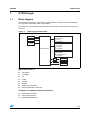
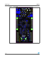
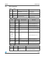
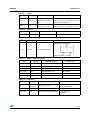
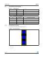
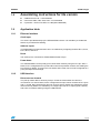
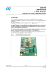
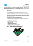
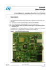
UM0282
User manual
STR9 Dongle hardware description
Introduction
This user manual provides a hardware description of both versions of the STR9 Dongle:
■
STEVAL-IFD001V1 (full version)
■
STEVAL-IFD001V2 (lite version)
Figure 1.
STR9 DONGLE (STEVAL-IFD001V2)
This document contains all the necessary assembly information to designers interested in
using STR9 Dongle including the block diagram, board schematics, footprints and PCB
layouts as well as the bill of materials and any additional assembly instructions.
June 2007
Rev 3
1/19
www.st.com
Contents
UM0282
Contents
1
STR9 Dongle . . . . . . . . . . . . . . . . . . . . . . . . . . . . . . . . . . . . . . . . . . . . . . . 3
1.1
Block diagram . . . . . . . . . . . . . . . . . . . . . . . . . . . . . . . . . . . . . . . . . . . . . . . 3
1.2
Schematics . . . . . . . . . . . . . . . . . . . . . . . . . . . . . . . . . . . . . . . . . . . . . . . . . 4
1.2.1
1.3
Suppliers . . . . . . . . . . . . . . . . . . . . . . . . . . . . . . . . . . . . . . . . . . . . . . . . . . 9
1.4
Used footprints . . . . . . . . . . . . . . . . . . . . . . . . . . . . . . . . . . . . . . . . . . . . . 10
1.5
PCB layout . . . . . . . . . . . . . . . . . . . . . . . . . . . . . . . . . . . . . . . . . . . . . . . . 11
1.6
Bill of materials . . . . . . . . . . . . . . . . . . . . . . . . . . . . . . . . . . . . . . . . . . . . . 13
1.7
Assembling instructions . . . . . . . . . . . . . . . . . . . . . . . . . . . . . . . . . . . . . . 16
1.7.1
2
2/19
Pin connections . . . . . . . . . . . . . . . . . . . . . . . . . . . . . . . . . . . . . . . . . . . . 8
Assembling of resistors . . . . . . . . . . . . . . . . . . . . . . . . . . . . . . . . . . . . . 16
1.8
Assembling instructions for lite version . . . . . . . . . . . . . . . . . . . . . . . . . . 17
1.9
Application hints . . . . . . . . . . . . . . . . . . . . . . . . . . . . . . . . . . . . . . . . . . . . 17
1.9.1
Ethernet interface . . . . . . . . . . . . . . . . . . . . . . . . . . . . . . . . . . . . . . . . . 17
1.9.2
USB interface . . . . . . . . . . . . . . . . . . . . . . . . . . . . . . . . . . . . . . . . . . . . . 17
Revision history . . . . . . . . . . . . . . . . . . . . . . . . . . . . . . . . . . . . . . . . . . . 18
UM0282
STR9 Dongle
1
STR9 Dongle
1.1
Block diagram
This board is based on an STR912FAW34, STR912FAW42 or STR912FAW44 microcontroller
which provides calculation power up to 90MIPS.
STR912FAW34, STR912FAW42 and STR912FAW44 are referred to STR912FAWxx throughout the
document.
Figure 2.
STR9 Dongle block diagram
3.3V
ANALOG_CONNECTOR
10 × GPIO
8 × Ain
2 × ExtINT
Power
1.8V
JTAG
4 × Buttons
4 × LEDs
STR912FAWxx
DIGITAL_CONNECTOR
16 × GPIO
I2C & SPI
2 × ExtINT
EXTENDED_CONNECTOR
16 × GPIO
3 × UART & SPI
6 × ExtINT
CAN
CAN
PHY
ETHERNET
USB
Main board features
●
42x GPIOs
●
3x UARTs
●
I2C
●
2x SPI
●
1x CAN
●
8x ADC
●
USB slave (full-speed)
●
Ethernet (STE100 or STE101)
Examples of available extended extensions:
●
STR9 Flash Extension
●
STR9 LCD Extension
●
STR9 MEMS Extension
3/19
D
C
1
C118
100nF
3V3
R102
10K
EMI_ALE
EMI_RD
EMI_WRH
EMI_WR/WRL
RESET_OUT
RESET_IN
MCU_X1
MCU_X2
B11
RESET
RESET_IN
74
75
22
21
100
89
RESET_OUT
RESET_IN
12
18
25
27
70
77
79
80
P50
P51
PHY_CLK
MII_TX_EN
P54
P55
B
MII_TX_CLK
P01
MII_RXD0
MII_RXD1
MII_RXD2
MII_RXD3
MII_RX_CLK
MII_RX_DV
P00
P01
P02
P03
P04
P05
P06
P07
P50
P51
P52
P53
P54
P55
P56
P57
16pF
C114
16pF
C115
X1
25MHz
CM5032@25MHz
P60
P61
P62
P63
104
103
2
1
MII_RX_ER
MII_TXD0
MII_TXD1
MII_TXD2
MII_TXD3
MII_COL
MII_CRS
MII_MDC
P10
P11
P12
P13
P14
P15
P16
P17
P60
P61
P62
P63
P64
P65
P66
P67
2
4
1
29
31
19
20
83
84
92
93
3
2
P70
P71
P72
P73
MCU_X1
MCU_X2
TRST
TCK
TMS
TDI
TDO
RTCK
MII_MDIO
USBUSB+
RTC-X2
RTC-X1
RTC_TAMPER1
RTC_X2
X2
32KHz
MC-146
R101
1M
MCU_X2
RTC_X1
MCU_X1
8pF
C116
8pF
C117
4
1
67
69
71
76
78
85
88
90
2
3
2
98
99
101
106
109
110
114
116
P22
P23
P24
P25
P26
P27
P20
P21
P22
P23
P24
P25
P26
P27
5
6
7
13
14
15
118
119
P75
P76
P77
P70
P71
P72
P73
P74
P75
P76
P77
10
11
33
35
37
45
53
54
P30
P31
P32
P33
P34
P35
P36
P37
55
59
60
61
63
65
66
68
P30
P31
P32
P33
P34
P35
P36
P37
26
28
30
32
34
36
38
44
P80
P81
P82
P83
P84
P85
P86
P87
P80
P81
P82
P83
P84
P85
P86
P87
P40
P41
P42
P43
P44
P45
P46
P47
3
2
1
128
127
126
125
124
P40
P41
P42
P43
P44
P45
P46
P47
P90
P91
P92
P93
P94
P95
P96
P97
46
47
50
51
52
58
62
64
4/19
P90
P91
P92
P93
P94
P95
P96
P97
94
95
96
41
42
91
107
108
111
115
117
97
3
RTC_X2
X2B
Q32
MII_MDIO
USB_DUSB_D+
RTC_X2
RTC_X1
JTRST
JTCK
JTMS
JTDI
JTDO
JRTCK
U1A
STR912FW44X6
RTC_X1
3
C105
100nF
3V3
3V3AN
1V8
39
123
122
4
81
49
17
112
113
82
48
16
C106
100nF
C101
100nF
C108
100nF
8
24
40
56
72
87
105
121
3V3
C103
100nF
C110
100nF
C104
100nF
C111
100nF
C112
100nF
4
STR9_DONGLE [MCU.sch]
STR912FW44X6
1V8
9
23
43
57
73
86
102
120
C102
100nF
C109
100nF
VCCQ
VCCQ
VCCQ(RTC)
VCCQ
VCCQ
VDD
VCCQ
VDD VCCQ(PLL)
VDD
VCCQ
VDD
VSSQ
AVREF
VSSQ
AVDD VSSQ(RTC)
AGND
VSSQ
VSSQ
VSSQ
VSSQ(PCLL)
VBAT
VSSQ
VSS
VSS
VSS
VSS
U1B
C107
100nF
3V3
4
D
C
B
A
Figure 3.
2
1.2
1
A
1
STR9 Dongle
UM0282
Schematics
Schematics 1 of 4
1
2
C05
100nF
10V
Max.16V
1
Vin
OUT
FB
Vout
LF18xDT
PW02
C03
22nF
L5973D
R03
4k7
PW01
VREF
VCC
SYNC
COMP
2
1
5
3
Tantal
(A,B)
C04
100uF 10V
Tantal
(C,D,E)
C06
2.2uF
C07
10nF
Max.500mA 1V8
STPS140A
L0133uH
D03 1A, 40V
MSS6132-333MLC
R02
3k3
R01
5k6
3V3
LD01
Red
2.0V
R04
300
->4mA
STR9_DONGLE [Power.sch]
B
4
D
C09
10nF
3V3
C02
220pF
C01
10uF
6
8
2
4
A
D
C08
10uF
35V
Tantal/Ceramic
(C,D,E)
D04
SMAJ24A
Transil [24V]
Vin
4
C
Tantal
(A,B)
Vin
3V3AN
1A, 40V
D01 STPS140A
D02
L02 3.3uH
1
2
3
0603PS-332KLC
3V3
5-24V
CN0
K375A
1A, 60V
STPS160A
3
C
B
USB5V
2
INH
GND
GND
3
7
9
GND
3
1
2
Figure 4.
A
1
UM0282
STR9 Dongle
Schematics 2 of 4
5/19
D
C
B
3V3
3V3
C30
10nF
JRTCK
JTCK
2
P50
P51
3V3
10K
1
C40
10nF
R25 3V3
1
DEF=3
3
10K
R24 3V3
1
2
DEF=3
3
10K
1
2
3
4
10K
10K
SN65HVD230
D
GND
VCC
R
RS
CANH
CANL
Vref
10K
R27
R28
10K
10K
R26
R22
R23
C50
10nF
U9
3V3
3V3
8
7
6
5
3V3
1
3
5
7
9
11
13
15
17
19
CN3
JTAG
1
3
5
7
9
11
13
15
17
19
CN2
2
4
6
8
10
12
14
16
18
20
2
4
6
8
10
12
14
16
18
20
3V3
R20
C90
100nF
EXTENDED_CON
CAN_RS
CAN_H
CAN_L
3V3
P90
P92
P94
P95
P32
P96
P97
P36
JTRST
JTDI
JTMS
JTCK
JRTCK
JTDO
RESET_IN
DBGRQ
DBGACK
3V3
P91
P93
P30
P31
P33
P34
P35
P37
0
2
CAN_L
R90
120
CAN
1
3
5
CN9
2
4
6
8
10
12
14
16
18
20
2
4
6
8
10
12
14
16
18
20
2
4
6
R91
10K
P81
P83
P84
P85
P86
P25
P27
P55
3V3
CAN_RS
CAN_H
ANALOG_CON
1
3
5
7
9
11
13
15
17
19
CN5
DIGITAL_CON
1
3
5
7
9
11
13
15
17
19
CN4
5-6 HI/LOW speed
P40
P41
P42
P43
P44
P45
P46
P47
P77
P76
3V3
P80
P82
P22
P23
P24
P87
P26
P54
USB_A
Vbus
DD+
GND
SH1
SH2
CN6
USB_1X90A
B85
LEFT
P70
1
2
3
4
5
6
3V3
R85
10K
2
1
3
C61
R61
USB5V
1M
4.7nF
C85
10nF
36
36
USB_PULL_UP
R62
R63
B86
UP
P71
3V3
R86
10K
2
1
250
-> 4mA
R84
300
-> 4mA
R83
300
-> 4mA
R82
330
-> 4mA
R81
C87
10nF
10k
1k5
R67
B88
RIGHT
P73
T2
3 BC846 2
36k
R65
T1
3 BC846 2
R64
4
P75
R66
47k
3V3
C88
10nF
USB_PULL_UP
3V3
4
STR9_DONGLE [Connectors.sch]
3V3
LD84 2.3V
green
1
2
P62
LD83 2.1V
yellow
1
2
P63
LD82 2.1V
yellow
1
2
P60
LD81 2.0V
red
1
2
P61
B87
DOWN
USB_DUSB5V
USB_D+
3V3
C86
10nF
P72
3V3
R87
10K
2
1
A
3
P6x - 8mA max.
JTRST
2
1
1
1
R88
10K
6/19
2
Note:
1
D
C
B
A
Figure 5.
R21 3V3
1
2
DEF=1
3
STR9 Dongle
UM0282
Schematics 3 of 4
Refer to Section 1.2.1 on page 8 for pin connections of CN3, CN4 and CN5 connectors.
D
C
B
A
3V3
47
46
44
43
51
48
49
59
60
42
41
61
MII_RXD0
MII_RXD1
MII_RXD2
MII_RXD3
MII_RX_ER
MII_RX_DV
MII_RX_CLK
MII_COL
MII_CRS
MII_MDC
MII_MDIO
100nF
C710
3V3
MDIX_DIS
54
53
MII_TX_EN
MII_TX_CLK
1
TX+
TX-
8
30
31
32
26
33
55
56
57
58
52
MII_TXD0
MII_TXD1
MII_TXD2
MII_TXD3
1
2
3
3V3
U71
I/O1 I/O3
REF2 REF1
I/O2 I/O4
DALC208SC6
NC
MDIX_DIS
CF2
SCLK
TEST
TEST_SE
MDC
MDIO
MDINT
COL
CRS
RX_DV
RX_CLK
RXD0
RXD1
RXD2
RXD3
RXD4/RX_ER
TX_EN
TX_CLK
TXD0
TXD1
TXD2
TXD3
TXD4/TX_ER
U7
E-STE101P
C702
100nF
MII_AVDD
MLS0805-4S4-300
L702
PHY_CLK
12
X1
VCCE/I
VCCE/I
VCCE/I
39
45
62
GNDE
GNDE/I
GNDE/I
4
5
6
25
40
50
C703
100nF
11
X2
VCCA
VCCA
VCCA
VCCA
NC
RX-
RX+
MII_AVCC
9
13
16
17
22
MLS0805-4S4-300
C701
100nF
3V3
RESET
RIP
CFG0
CFG1
LEDr10
LEDtr
LEDl
LEDc
LEDs
RXP
RXN
TXP
TXN
R720B 10K
R720A 10K
C705
100nF
2
CFG1
CFG0
FDE
MF0
MF1
MF2
MF3
MF4
PWRDWN
C704
100nF
LED10
LEDTR
LEDL
LEDC
LEDS
CFG0
CFG1
RESET_OUT
P01 R719
MF0
MF1
MF2
MF3
MF4
FDE
38
37
36
35
34
64
63
28
29
27
5
4
3
2
1
6
10K
R722 3V3
1
2
DEF=1
3
10K
MF1
MF0
RX+
RX-
19
18
R721 3V3
1
2
DEF=1
3
TX+
TX-
21
23
C714
10nF
3V3
10K
R724 3V3
1
2
DEF=1
3
10K
R723 3V3
1
2
DEF=1
3
10K
C715
10nF
MF3
MF2
10K
R726 3V3
1
2
DEF=3
3
10K
R725 3V3
1
2
DEF=1
3
RX-
R710
100
STE100
RX+
C711
100nF
3
FDE
MF4
C712
100nF
MII_AVCC
RXR
2
TX-
10K
R728 3V3
1
2
DEF=3
3
10K
RXR
LEDL
10K
R729 3V3
1
MDIX_DIS2
DEF=3
3
LEDTR
R716
240
R715
1k5
ADDR3
Yellow
3V3
LED10
R717
4k7
ADDR4
R713
1k5
ADDR2
Green
RX-
RX+
TX-
TX+
C708
10pF
STE100
TX+
R708
51
STE100
MII_AVDD
4
R712
4k7
ADDR1
LEDC
8
7
6
5
4
3
2
1
J00-0086
C709
0.1uF
TXT
R709
0
STE101
MII_AVDD
R711
4k7
ADDR0
LEDS
4
STR9_DONGLE [Ethernet.sch]
R714
240
C707
10pF
STE100
TX-
R707
51
STE100
MII_AVDD
1.414:1
1.414:1
C706
0.1uF
J00-0086
RD-
CT
RD+
TD-
CT
TD+
CN7
R727 3V3
1
2
DEF=3
3
8
7
6
5
3
4
1
TXT
TX+
C713
100nF
12
15
Iref
GNDA
GNDA
GNDA
GNDA
GNDA
7
10
14
20
24
11
MII_AVCC
L701
10
3
9
2
13
D
C
B
A
Figure 6.
14
1
UM0282
STR9 Dongle
Schematics 4 of 4
7/19
STR9 Dongle
1.2.1
UM0282
Pin connections
The following tables show the pin connections for the three connectors ANALOG_CON
(CN5), DIGITAL_CON (CN4) and EXTENDED_CON (CN3). These are shown in Figure 5 on
page 6.
Table 1.
Pin
GPIO
INT
UART
I2C
SPI
ADC
P40
In/Out
-
-
-
-
ADC0
P41
In/Out
-
-
-
-
ADC1
P42
In/Out
-
-
-
-
ADC2
P43
In/Out
-
-
-
-
ADC3
P44
In/Out
-
-
-
-
ADC4
P45
In/Out
-
-
-
-
ADC5
P46
In/Out
-
-
-
-
ADC6
P47
In/Out
-
-
-
-
ADC7
P77
In/Out
EXINT31
-
-
-
-
P76
In/Out
EXINT30
-
-
-
-
Table 2.
Pin
8/19
Analog connector, ANALOG_CON (CN5)
Digital connector, DIGITAL_CON (CN4)
GPIO
INT
UART
I2C
SPI
ADC
P80
In/Out
-
-
-
-
-
P81
In/Out
-
-
-
-
-
P82
In/Out
-
-
-
-
-
P83
In/Out
-
-
-
-
-
P22
In/Out
-
-
-
I2C1_CLK
-
P84
In/Out
-
-
-
-
-
P23
In/Out
-
-
-
I2C1_DATA
-
P85
In/Out
-
-
-
-
-
P24
In/Out
P86
In/Out
-
-
-
-
-
P87
In/Out
-
-
-
-
-
P25
In/Out
-
-
SSP0_MOSI -
-
P26
In/Out
-
-
SSP0_MISO -
-
P27
In/Out
-
-
SSP0_NSS
-
-
P54
In/Out
EXINT12
-
-
-
-
P55
In/Out
EXINT13
-
-
-
-
SSP0_SCLK
UM0282
STR9 Dongle
Table 3.
Extended connector, EXTENDED_CON (CN3)
Pin
1.3
GPIO
INT
UART
I2C
SPI
ADC
P90
In/Out
-
-
-
-
-
P91
In/Out
-
-
-
-
-
P92
In/Out
-
-
-
-
-
P93
In/Out
-
-
-
-
-
P94
In/Out
-
-
-
-
-
P30
In/Out
-
UART0_RX
UART2_TX
-
-
-
P95
In/Out
-
-
-
-
-
P31
In/Out
-
UART2_RX
UART0_TX
-
-
-
P32
In/Out
EXINT2
UART1_RX
-
-
-
P33
In/Out
EXINT3
UART1_TX
-
-
-
P96
In/Out
-
-
-
-
-
P34
In/Out
EXINT4
-
SSP0_SCLK -
-
P97
In/Out
-
-
-
-
-
P35
In/Out
EXINT5
-
SSP0_MISO -
-
P36
In/Out
EXINT6
-
SSP0_MOSI -
-
P37
In/Out
EXINT7
-
SSP0_NSS
-
-
Suppliers
KOALA
www.koala.cz
GME
www.gme.cz
FARNELL
www.farnellinone.cz
TAIYO YUDEN
www.t-vuden.com
WURTH ELEKTRONIK:
www.wuerth-elektronik.de
PULSE
www.pulseeng.com/
COILCRAFT
www.coilcraft.com
9/19
STR9 Dongle
1.4
UM0282
Used footprints
www.koala.cz: MC-146
www.koala.cz: CM5032
www.coilcraft.com: 0603PS-332KLC
10/19
UM0282
1.5
STR9 Dongle
PCB layout
Figure 7.
Top view
11/19
STR9 Dongle
Figure 8.
12/19
UM0282
Bottom view
UM0282
1.6
STR9 Dongle
Bill of materials
Table 4.
Chips
Part
Package
Detail description
Order code
U1
LQFP128
STR912FAW34, STR912FAW42,
STR912FAW44
ST: STR912FAW34x6,
STR912FAW42x6,
STR912FAW44x6
U7
TQFP64
Ethernet physical layer
ST: STE100 or STE101
U71
SOT23-6L
DALC208 diode protection
ST: DALC208SC6
U9
SO8
CAN transceiver (3V)
Farnell: 501-1954
(SN65HVD230-232)
Table 5.
Capacitors
Part
Package
Detail description
Order code
C114, C115,
0603
18 pF (16-22 pF), ceramic
C116, C117
0603
10 pF (8-16 pF), ceramic
Farnell: 422-6768 (NPO, 50 V)
C707, C708
C30, C40, C50
0603
10 pF
Farnell: 422-6768 (NPO, 50 V)
C03
0603
22 pF
Farnell: 422-6770 (NPO, 50 V)
C02
0603
220 pF
Farnell: 422-6811 (NPO, 50 V)
C61
0603
4.7 nF, ceramic
Farnell: 422-6926 (X7R, 50 V)
C07, C09,
C714-C715,
C85-C88
0603
10 nF
Farnell: 422-6938 (X7R, 50 V)
C05, C118,
C701-C705,
C706, C709,
C711-C713,
C90,
C101-C112,
C710
0603
100 nF
Farnell: 422-6859 (X7R, 16 V)
C06
AB
2.2 µF
Farnell: 757-720 (STD, 10 V)
C08
AB
10 µF
Farnell: 331-3888 (STD, 10 V)
C01
CDE
10 µF, 35V, Tantal or ceramic
Farnell: 331-4145 (LowESR, 35 V)
Taiyo: CE GMK325 F106ZH-T
C04
CDE
100 µF, 10V, Tantal
Farnell: 331-4066 (LowESR, 10 V)
Table 6.
Xtals
Part
Package
Detail description
Order code
X1
-
25 MHz
KOALA: 25MHz CM5032
X2
X2B
-
32 kHz
KOALA: 32.768 MC146
GM: 131-082 (Q32.768KHZM)
13/19
STR9 Dongle
UM0282
Table 7.
Resistors
Part
Package
Order code
R709, R20
0603
0
GM: R0603-0R
R62-R63
0603
36
GM: R0603-36R
R707, R708
0603
51
GM: R0603-51R
R710
0603
100
GM: R0603-100R
R90
0603
120
GM: R0603-120R
R714, R716
0603
240
GM: R0603-240R
R84
0603
270
GM: R0603-240R
R82, R83,
0603
390
GM: R0603-300R
R81, R04
0603
330
GM: R0603-330R
R67,
R713, R715
0603
1k5
GM: R0603-1K5
R02
0603
3k3
GM: R0603-3K3
R711, R712, R717,
R03
0603
4k7
GM: R0603-4K7
R01
0603
5k6
GM: R0603-5K6
R102, R64
R719,
R721-R729,
R91,
R85-R88,
R21-R28
0603
10k
GM: R0603-10K
R101, R61
0603
1M
GM: R0603-1M
R65
0603
36k
GM: R0603-36K
R66
0603
47k
GM: R0603-47K
R720A, 720B
0603
10k
GM: R0603-10K 1%
Table 8.
Part
Connectors
Package
Detail description
Order code
CN0
TAP_2.5mm
Connector
GM: K375A
CN2, CN3
2.54mm
Connector, 2x10pins
GM: MLW20G
CN4
2.54mm
2x10pin header
GM: S2G20
CN5
2.54mm
2x10pin header
GM: BL220G
CN6
USB_A
USB connector
GM: USB-1X90A
Ethernet Connector with
integrated transformer
Pulse: J00-0086
6pin header
GM: S2G20 (cut to 6pin)
CN7
CN9
14/19
Detail description
2.54mm
UM0282
STR9 Dongle
Table 9.
Power
Part
Package
Detail description
Order code (reference)
PW01
SO8cool
VOUT = 3.3 V,
typ. 200 mA, max. 500
mA
ST: E-L5973D
(VINmax = 35 V, Imax = 2.5 A, Rth = 40 C/W
Use external supply 5-24V)
PW02
DPAK
VOUT = 1.8 V,
typ. 100 mA, 0.15 W
ST: LF18xDT
(VINmax =16 V, Imax = 1 A, Rth = 8 C/W)
Table 10.
Buttons
Part
Package
B11, B85-B88
Table 11.
Part
-
Detail description
Order code (reference)
Button
GM: P-DT2112C
Transistors
Package
Detail description
Order code
GM: BC846A or compatible
T1,T2
SOT23-3
NPN universal transistor
1-Base, 2-Emitter, 3-Collector
Table 12.
LEDs & diodes & tranzils
Part
Package
Detail description
Order code
D01, D03
SMA
Shottky diode 1 A, 40 V
ST: STPS140A
D02
SMA
Shottky diode 1 A, 60 V
ST: STPS160A
D04
SMA
Transil, 24 V
ST: SMAJ24A
LD01, LD81
0805
Red LED diode, 2.0 V
GM: 960-024
LD82, LD83
0805
Yellow LED diode, 2.1 V
GM: 960-025
LD84
0805
Green LED diode, 2.3 V
GM: 960-023
Table 13.
Part
Inductors
Package
Detail description
Order code
L01
MSS6132
6.1x6.1mm
33 µH, Irms = 1.6 A
Coilcraft: MSS6132-333MLC
(12-39 µH available)
L02
0603
3.3 µH, Irms = 0.5 A
Coilcraft: 0603PS-332KLC
L701, L702
0805
SMD-Ferrit 33 µH: 30@100 MHz
Wurth Elektronik:
74279206
15/19
STR9 Dongle
1.7
UM0282
Assembling instructions
Table 14.
JTAG with IAR
Part
Assembled
R21
YES
Position 1-2
R24, R25
YES
Position 2-3
R27, R28
NO
R20
YES
Table 15.
Configuration with STE101P
Part
1.7.1
Configuration / Comment
Assembled
Configuration / Comment
R710
NO
R707. R708
NO
R709
YES
R721-R725
YES
Position 1-2
R726-R729
YES
Position 2-3
Assembling of resistors
The marking (from top to bottom) is following: 3-2-1.
Figure 9.
Resistor assembly
Possible assembling positions are:
16/19
a)
1-2
b)
2-3
UM0282
1.8
STR9 Dongle
Assembling instructions for lite version
●
CAN transceiver U9 – not assembled
●
Connectors CN3, CN4, CN5, CN9 – not assembled
●
Crystal X2 – use this one GM: 131-082 (Q32.768KHZM)
1.9
Application hints
1.9.1
Ethernet interface
Clock input
The clock is provided directly by the STR912FAWxx device. It is mandatory to enable this
feature on pin P52 before starting.
Address inputs
The DMA address is fixed and set to 0x10. It is defined by configuring resistors R711, R712,
R713, R715, and R717.
Reset
The reset input is connected to STR912FAWxx Reset-out pin.
Power-down
The STR912FAWxx can be quickly put in Power-down mode by using the P01 pin. After a
Reset, P01 is configured as an input and R719 acts as a pull-down resistor, thus making the
PHY active by default. To put the PHY into Power-down mode, P01 must be configured as a
push-pull output and held High.
1.9.2
USB interface
Disconnect on demand
The pull-up resistor R67 is driven by P75 pin. It tells the host whether the device is
connected or not. After a Reset, P75 is configured as an input, which means that T2 is open
and T1 closed. R67 consequently does not act as a pull-up resistor thus making the device
disconnected by default. It is mandatory to configure pin P75 as an output (open-collector)
and hold it Low before starting using the USB interface.
17/19
Revision history
2
UM0282
Revision history
Table 16.
Document revision history
Date
Revision
19-Jan-2007
1
Initial release.
24-May-2007
2
Section 1.9: Application hints added.
3
Figure 1: STR9 DONGLE (STEVAL-IFD001V2) updated.
Root part numbers changed from STR912FW42xx and
STR912FW44x to STR912FAW34, STR912FAW42 and
STR912FAW44 throughout the document.
Table 4: Chips updated.
19-June-2007
18/19
Changes
UM0282
Please Read Carefully:
Information in this document is provided solely in connection with ST products. STMicroelectronics NV and its subsidiaries (“ST”) reserve the
right to make changes, corrections, modifications or improvements, to this document, and the products and services described herein at any
time, without notice.
All ST products are sold pursuant to ST’s terms and conditions of sale.
Purchasers are solely responsible for the choice, selection and use of the ST products and services described herein, and ST assumes no
liability whatsoever relating to the choice, selection or use of the ST products and services described herein.
No license, express or implied, by estoppel or otherwise, to any intellectual property rights is granted under this document. If any part of this
document refers to any third party products or services it shall not be deemed a license grant by ST for the use of such third party products
or services, or any intellectual property contained therein or considered as a warranty covering the use in any manner whatsoever of such
third party products or services or any intellectual property contained therein.
UNLESS OTHERWISE SET FORTH IN ST’S TERMS AND CONDITIONS OF SALE ST DISCLAIMS ANY EXPRESS OR IMPLIED
WARRANTY WITH RESPECT TO THE USE AND/OR SALE OF ST PRODUCTS INCLUDING WITHOUT LIMITATION IMPLIED
WARRANTIES OF MERCHANTABILITY, FITNESS FOR A PARTICULAR PURPOSE (AND THEIR EQUIVALENTS UNDER THE LAWS
OF ANY JURISDICTION), OR INFRINGEMENT OF ANY PATENT, COPYRIGHT OR OTHER INTELLECTUAL PROPERTY RIGHT.
UNLESS EXPRESSLY APPROVED IN WRITING BY AN AUTHORIZED ST REPRESENTATIVE, ST PRODUCTS ARE NOT
RECOMMENDED, AUTHORIZED OR WARRANTED FOR USE IN MILITARY, AIR CRAFT, SPACE, LIFE SAVING, OR LIFE SUSTAINING
APPLICATIONS, NOR IN PRODUCTS OR SYSTEMS WHERE FAILURE OR MALFUNCTION MAY RESULT IN PERSONAL INJURY,
DEATH, OR SEVERE PROPERTY OR ENVIRONMENTAL DAMAGE. ST PRODUCTS WHICH ARE NOT SPECIFIED AS "AUTOMOTIVE
GRADE" MAY ONLY BE USED IN AUTOMOTIVE APPLICATIONS AT USER’S OWN RISK.
Resale of ST products with provisions different from the statements and/or technical features set forth in this document shall immediately void
any warranty granted by ST for the ST product or service described herein and shall not create or extend in any manner whatsoever, any
liability of ST.
ST and the ST logo are trademarks or registered trademarks of ST in various countries.
Information in this document supersedes and replaces all information previously supplied.
The ST logo is a registered trademark of STMicroelectronics. All other names are the property of their respective owners.
© 2007 STMicroelectronics - All rights reserved
STMicroelectronics group of companies
Australia - Belgium - Brazil - Canada - China - Czech Republic - Finland - France - Germany - Hong Kong - India - Israel - Italy - Japan Malaysia - Malta - Morocco - Singapore - Spain - Sweden - Switzerland - United Kingdom - United States of America
www.st.com
19/19