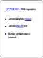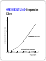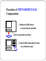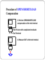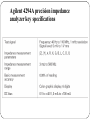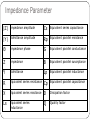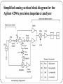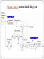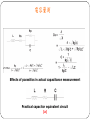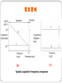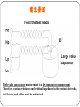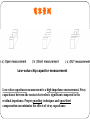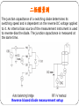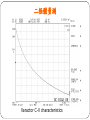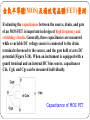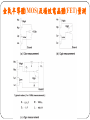
1
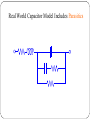
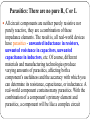
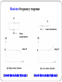
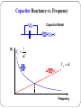
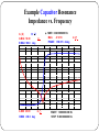
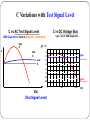
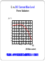
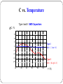
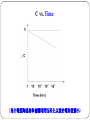
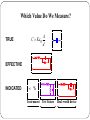
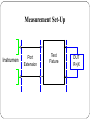
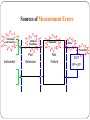
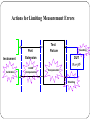
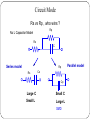
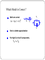
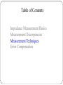
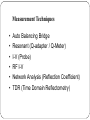
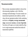
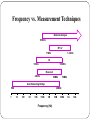
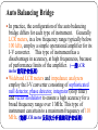
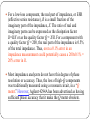
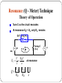
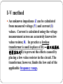
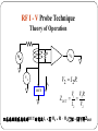
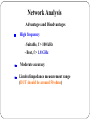
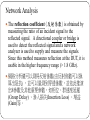
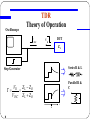
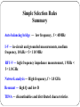
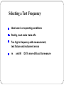
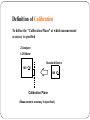
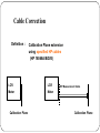
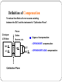
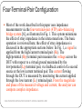
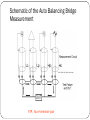
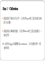
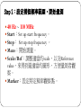
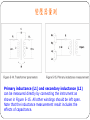
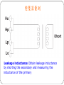
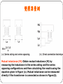
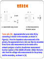
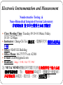
Electronic Instrumentation and Measurement Nondestructive Testing & Nano-Biomedical Integrated System Laboratory (非破壞檢測 暨 奈米生醫整合系統 實驗室) Class Meeting Time: Tuesday 09:10~10:00am, Friday 10:10~12:00am Instructor: Cheng-Chi Tai (戴政祺,電機研究所 儀器系統與晶 片組) Office: 92605 EE Building Office Phone: 06-2757575 ext. 62388 E-mail: [email protected] Handouts: http://140.116.177.248/ 註: NDT & NBMIS實驗室研究題目包括生物醫學電子整合系統 (腫瘤電磁熱療、等) ;電磁控制(3D磁浮、膠囊型內視鏡)與; 非破壞檢測(渦電流、超音波、音射、局部放電)等。 References • IEEE Instrumentation and Measurement, Review of Scientific Instrumentation 等中英文期刊。 • 儀器總覽:電子測試儀器,國科會精密儀器發展中心,1998。 • “LCR/Impedance Measurement Basics”, HP Company 1997 • “Impedance Measurement Handbook”, HP Company 2000 • “HP4294A Precision Impedance Analyzer Programming Manual (程式設計 手冊)”, HP • “HP4294A Precision Impedance Analyzer Operation Manual”, HP • “8 Hints for Successful Impedance Measurements”, Agilent • “8 Hints For Solving Common Debugging Problems With Your Logic Analyzer” , Agilent • “Tektronix Logic Analyzer Family User Manual”, Tektronix. • “Time Domain Reflectometry Theory”, Agilent App Note 1304-2 • “Techniques for Measuring the Electrical Resistivity of Bulk Materials”, Mary Anne Tupta, Keithley. • “Understanding the Basics of Electrical Measurements”, Derek Maclachlan, Keithley. Table of Contents Ch13. LCR Meter and Impedance Analyzer Impedance Measurement Basics Measurement Discrepancies Measurement Techniques Error Compensation 阻抗分析儀、時域反射儀、網路分析儀 為了使通訊傳輸頻寬更大,電子產品日益走向高頻化,訊 號傳輸模式必須以微波(Microwave)觀念去思考。頻率愈高, 所傳輸的AC信號就會有傳輸線(Transmission line)的效應, 於是有一個重要參數—阻抗(Impedance)的分析就愈顯重 要。 阻抗由電阻(R, resistance) 、電容(C, Capcitance) 、及電感(L, Inductance)組成。阻抗並不是一個絕對值,而是一個隨頻 率變化的函數。 用來分析阻抗的儀器,主要有阻抗分析儀 (ZA, Impedance Analyzer)、時域反射儀(TDR, Time Domain reflectrometer)、 及網路分析儀(NA, Network Analyzer) 或向量網路分析儀 (VNA)。 直流、1 MHz、1 GHz 高頻下運作,電子電路之特性與直流下的的現象不 同。 當頻率超過 1 MHz後,電路的電器特性會呈現集總 (Lumped, 塊狀)現象,會有寄生現象及未知損耗產 生。 當頻率超過 1 GHz後,會有所謂傳輸線現象 (Transmission line),此時分析元件及電路,就要使 用阻抗(impedance)及其相關的參數來作分析。 Impedance definition • Impedance is the total opposition a device or circuit offers to the flow of a periodic current. • AC test signal (amplitude and frequency) • Includes real and imaginary elements Z=R+jX Y=G+jB Impedance definition Impedance Measurement Plane DUT Inductive +j Z R jX Z |Z| Imaginary Axis Capacitive Resistive Real Axis Z: Impedance R: Resistance -j Z R X 2 2 (阻抗) R Z cos (電阻) X Z sin (電抗) X tan R X L 2fL L (感抗, Inductance) 1 X C 1 /( 2fC ) 1 /(C ) (容抗, Capacitance) Admittance Measurement Plane Y=1/Z Capacitive +j DUT |Y| Inductive Imaginary Axis Y G jB Y Conductive Y G 2 B 2 (導納) Real Axis G Y cos (電導) Y: Admittance (S, Siemen) (電納) B Y sin G: Conductance B: Susceptance 1 B -j tan G To find the impedance, we need to measure at least two values because impedance is a complex quantity. Many modern impedance measuring instruments measure the real and the imaginary parts of an impedance vector and then convert them into the desired parameters such as |Z|, θ, |Y|, R, X, G, B, and Q. Table of Contents Impedance Measurement Basics Measurement Discrepancies Measurement Techniques Error Compensation Measurement Discrepancy Reasons (量測不一致的原因) Component Dependency Factors True, Effective, and Indicated Values Measurement Errors Circuit Mode (Translation Equations) Measurement Discrepancy Reasons — Component Dependency Factors — Test signal frequency (測試信號頻率) Test signal level (測試信號準位) DC bias, voltage and current (偏壓、電流、電壓) Environment (temperature, humidity, etc.) 溫溼度環 境 Component‘s current state Aging (老化) Real World Capacitor Model Includes Parasitics Parasitics: There are no pure R, C or L All circuit components are neither purely resistive nor purely reactive, they are a combination of these impedance elements. The result is, all real-world devices have parasitics - unwanted inductance in resistors, unwanted resistance in capacitors, unwanted capacitance in inductors, etc. Of course, different materials and manufacturing technologies produce varying amounts of parasitics, affecting both a component’s usefulness and the accuracy with which you can determine its resistance, capacitance, or inductance. A real-world component contains many parasitics. With the combination of a component’s primary element and parasitics, a component will be like a complex circuit Quality and Dissipation Factors Different from the Q associated with resonators and filters. Energy stored Q= Energy lost = Xs Rs The better the component, then R Q 0 1 D= Q , mainly used for capacitors 1 1 X L X C BL BC Q D tan R R G G Resistor frequency response (高阻值電阻在高頻有電容效應) (低阻值電阻在高頻有電感效應) Inductor frequency response (General Inductor) (Inductor with high Core-loss) Capacitor Reactance vs. Frequency Capacitor Model |X| 1 XC C X L L Frequency Example Capacitor Resonance Impedance vs. Frequency MKR 6 320 000.000 Hz MAG 47.2113 PHASE 659.015 mdeg B: 0 A: |Z| A MAX 50.00 B MAX 100.0 deg A MIN 20.00 B MIN -100.0 deg m START 1 000 000.000 Hz STOP 15 000 000.000 Hz m C Variations with Test Signal Level C vs DC Voltage Bias C vs AC Test Signal Level Type I and II SMD Capacitors SMD Capacitors, Various dielectric constants K High K C C/% Mid K 2 Low K Type I 0 -2 NPO (low K) -4 -6 -8 -10 Type II -20 0 Vac (Test Signal Level) X7R (high K) 50 100 Vdc L vs. DC Current Bias Level Power Inductors L/% 2 0 -2 -4 -6 -8 -10 -20 0 50 100 Idc (DC Bias current) (電感核心材料的磁通量因為偏壓電流太大而飽和) 某些被動元件阻抗值與直流偏壓大小有關,有些 元件需要操作在某個偏壓下才能正確工作,此時 就需要有一個穩定的直流電源供應偏壓,以高介 電質的陶瓷電容為例,當偏壓改變時,相對應的 阻抗值就不同。一般而言,阻抗分析儀可以選擇 內建的方式直接在內部加入偏壓源,但對於網路 分析儀而言,則是加一個Bias Network或Bias Tee 在外部耦合直流及交流的信號。 C vs. Temperature Type I and II SMD Capacitors C/% 15 10 5 Type I 0 NPO (low K) -5 -10 -15 Type II -20 X7R (high K) -60 -20 20 60 100 140 T/ C C vs. Time (高介電值陶瓷材料會隨時間而老化以致於電容值變小) Which Value Do We Measure? A C K 0 d TRUE EFFECTIVE INDICATED +/- % Instrument Test fixture Real-world device True, effective, and indicated values A true value (真實值) is the value of a circuit component (resistor, inductor or capacitor) that excludes the defects of its parasitics. In many cases, the true value can be defined by a mathematical relationship involving the component’s physical composition. In the real-world, true values are only of academic interest. The effective value (有效值) takes into consideration the effects of a component’s parasitics. The effective value is the algebraic sum of the circuit component’s real and reactive vectors; thus, it is frequency dependent. The indicated value (指示值) is the value obtained with and displayed by the measurement instrument; it reflects the instrument’s inherent losses and inaccuracies. Indicated values always contain errors when compared to true or effective values. They also vary intrinsically from one measurement to another; their differences depend on a multitude of considerations. Comparing how closely an indicated value agrees with the effective value under a defined set of measurement conditions lets you judge the measurement’s quality. Measurement Set-Up Instrument Port Extension Test Fixture DUT R+jX Sources of Measurement Errors Measurement technique inaccuracies Port Extension complex residuals Fixture residuals RFI and other noise DUT stray and lead parasitics Sources of Measurement Errors Technique Inaccuracies Complex Residuals Residuals Noise Parasitics Instrument Port Test Extension Fixture DUT Rx + jXx Actions for Limiting Measurement Errors Instrument Port Extension Test Fixture Guarding DUT R x+ jXx Calibration LOAD Compensation Compensation Shielding What Do Instruments... Measure ? Calculate ? Approximate ? I-V Method Measured Direct Calculations Model based Approximations Reflection Coefficient Method x,y I, V Z= V I Z = Zo 1 + 1 - Ls , Lp, Cs, Cp, Rs or ESR, Rp, D, Q Rs DUT ? Rp Cp Cs Circuit Mode Requires Simplified Models Complete Capacitor Model Rs,Ls,Rp,Cp ? No L Capacitor Model Circuit Mode Rs vs Rp , who wins ? Rp No L Capacitor Model Rs C Series model Rp Rs Cs Cp Large C Small C Small L Large L SMD Parallel model Which Model is Correct ? Rp Both are correct 2 Cs = Cp ( 1 + D ) Rs Cs Cp One is a better approximation For high Q or low D components, Cp Cs Table of Contents Impedance Measurement Basics Measurement Discrepancies Measurement Techniques Error Compensation Measurement Techniques • Auto Balancing Bridge • Resonant (Q-adapter / Q-Meter) • I-V (Probe) • RF I-V • Network Analysis (Reflection Coefficient) • TDR (Time Domain Reflectometry) Measurement methods There are many measurement methods to choose from when measuring impedance, each of which has advantages and disadvantages. You must consider your measurement requirements and conditions, and then choose the most appropriate method, while considering such factors as frequency coverage, measurement range, measurement accuracy, and ease of operation. Your choice will require you to make tradeoffs as there is not a single measurement method that includes all measurement capabilities. Measurement Technique Topics • • • • Technique Selection Criteria Theory of Operation Advantages and Disadvantages of each technique Expanded connection information and theory for auto balancing bridge (r4 terminal pair) instruments • Error compensation to minimize measurement error Measurement Technique Selection Criteria • Frequency • DUT Impedance • Required measurement accuracy • Electrical test conditions • Measurement parameters • Physical characteristics of the DUT Frequency vs. Measurement Techniques Network Analysis 100KHz RF I-V 1 MHz 1.8 GHz I-V 10KHz 110MHz Resonant 22KHz 30MHz 70MHz Auto Balancing Bridge 5HZ 1 40MHz 10 100 1K 10K 100K 1M Frequency (Hz) 10M 100M 1G 10G Solution by Frequency Comparison 100M Auto Balancing Bridge 10M RF I-V 1M I-V (Probe) 100K Network Analysis Impedance (Ohms) 10K 1K 100 10 1 100m 10m 1m 10 100 1K 10K 100K 1M 10M 100M Frequency 1G 10G Hz Which is the best ? All are good Each has advantages and disadvantages Multiple techniques may be required Considering only measurement accuracy and ease of operation, the auto balancing bridge method is the best choice for measurements up to 110 MHz. For measurements from 100 MHz to 3 GHz, the RF I-V method has the best measurement capability, and from 3 GHz and up the network analysis is the recommended technique. Auto Balancing Bridge Theory of Operation Virtual ground H R2 L DUT V1 I I2 I = I2 + V2 I 2 R2 Z ( DUT ) V1 V1R2 I2 V2 V2 電橋方法:一般是標準實驗室使用, 高精準,但須針對高或低頻使用不 同電橋。 (DC to 300 MHz) Auto Balancing Bridge Advantages and Disadvantages Most accurate, basic accuracy 0.05% Widest measurement range C, L, D, Q, R, X, G, B, Z, Y, O,... Widest range of electrical test conditions Simple-to-use Low frequency, f < 40MHz 自動平衡電橋方法:一般用途(LCR meter, Z analyzer), 精準度高 Auto Balancing Bridge In practice, the configuration of the auto balancing bridge differs for each type of instrument. Generally LCR meters, in a low frequency range typically below 100 kHz, employ a simple operational amplifier for its I-V converter. This type of instrument has a disadvantage in accuracy, at high frequencies, because of performance limits of the amplifier. (一般LCR meter適用於較低頻) Wideband LCR meters and impedance analyzers employ the I-V converter consisting of sophisticated null detector, phase detector, integrator (loop filter) and vector modulator to ensure a high accuracy for a broad frequency range over 1 MHz. This type of instrument can attain to a maximum frequency of 110 MHz. (寬頻LCR meter及阻抗分析儀適用於較高頻) Performing High Q / Low D Measurement is Difficult +jX X1 Impedance of very high Q device X1 Q R1 R1 R Very small R, difficult to measure -jX (自動平衡電橋法不適合量高Q元件 改用Q-meter) For a low-loss component, the real part of impedance, or ESR (effective series resistance), R is a small fraction of the imaginary part of the impedance, X. The ratio of real and imaginary parts can be expressed as the dissipation factor D=R/X or as the quality factor Q = X/R. For a component with a quality factor Q = 200, the real part of the impedance is 0.5% of the total impedance. Thus, even a 0.1% error in an impedance measurement could potentially cause a 200x0.1% = 20% error in R. Most impedance analyzers do not have this degree of phase resolution or accuracy. Thus, the loss of high-Q components was traditionally measured using a resonant circuit, in a “Q meter.” However, Agilent 4294A has been advertised as having sufficient phase accuracy that it make the Q meter obsolete. Resonance (Q - Meter) Technique Theory of Operation Tune C so the circuit resonates At resonance XD = -XC, only RD remains DUT L (XD), R D OSC ~ e Tuning C (X c) I= e Z V RDV XC I e at resonance XD XC V Q RD RD e V V Resonance (Q - Meter) Technique When a circuit is adjusted to resonance by adjusting a tuning capacitor C, the unknown impedance LD and RD values are obtained from the test frequency, C value, and Q value. Q is measured directly using a voltmeter placed across the tuning capacitor. Because the loss of the measurement circuit is very low, Q values as high as 1000 can be measured. Other than the direct connection shown here, series and parallel connections are available for a wide range of impedance measurements. Resonant Method Advantages and Disadvantages Very good for high Q - low D measurements Requires reference coil for capacitors Limited L,C values accuracy Vector 75kHz - 30MHz automatic and fast easy to use limited compensation Scalar 22kHz - 70MHz manual and slow requires experienced user No compensation I-V (Probe) Advantages and Disadvantages Medium frequency, 10 kHz < f < 110 MHz Moderate accuracy and measurement range Grounded and in-circuit measurements Simple-to-use I-V法:配合探針,適用於量測電路板上之元件 I-V method An unknown impedance Z can be calculated from measured voltage (V) and current (I) values. Current is calculated using the voltage measurement across an accurately known low value resistor, R. In practice a lowloss transformer is used in place of R (一般以低損耗 變壓器取代R) to prevent the effects caused by placing a low value resistor in the circuit. The transformer, however, limits the low end of the applicable frequency range. RF I - V Probe Technique Theory of Operation R V1 I2 V2 V2 I 2 R DUT Z DUT V1 V1 R I 2 V2 以感應線圈感應通過DUT的電流I2 ,若 V1,R ,V2已知,則可得ZDUT RF I-V Theory of Operation High Impedance Test Head Voltage Detection Vi Current Detection Ro Vv Ro Low Impedance Test Head Vi Current Detection Voltage Detection Ro DUT Vv Ro DUT RF I-V While the RF I-V measurement method is based on the same principle as the I-V method, it is configured in a different way by using an impedance matched measurement circuit (50 Ω) and a precision coaxial test port for operation at higher frequencies. There are two types of the voltmeter and current meter arrangements; which are suited to low impedance and high impedance measurements. Impedance of the device under test (DUT) is derived from measured voltage and current values, as illustrated. The current that flows through the DUT is calculated from the voltage measurement across a known low value resistor, R. In practice, a low loss transformer is used in place of the low value resistor, R. The transformer limits the low end of the applicable frequency range. RF I-V Advantages and Disadvantages High frequency, 1MHz < f < 1.8GHz (or 3 GHz) Most accurate method at > 100 MHz Grounded device measurement RF I-V RF I-V 使用微波感應的方式,偵測進入待測物的向量 電壓及電流,從而得到阻抗值,工作原理近似於網路 分析儀。 因為感應線圈在高頻狀態反應較佳,因此低頻範圍較 自動平衡電橋窄(適於> 1 MHz至 3GHz) , 精確度也 較低。 使用前須做「校正+補償」 ,以去除纜線 、信號源 及接收器端的阻抗不匹配。 自動平衡電橋 vs. RF I-V Network Analysis (Reflection) Technique Theory of Operation VINC DUT VR Z L ZO VR VINC Z L ZO Z0是傳輸線特性阻抗,一般 為50 W。由反射係數可以知 道ZL與Z0的接近程度 (The closeness of ZL to Z0) NA法:以信號反射原理找出待測物的阻抗,主要應用於射頻及微 波量測(i.e.高頻)。由量測到的反射係數換算出阻抗(ZL)大小。 Network Analysis Advantages and Disadvantages High frequency - Suitable, f > 100 kHz - Best, f > 1.8 GHz Moderate accuracy Limited impedance measurement range (DUT should be around 50 ohms) Network Analysis The reflection coefficient (反射係數) is obtained by measuring the ratio of an incident signal to the reflected signal. A directional coupler or bridge is used to detect the reflected signal and a network analyzer is used to supply and measure the signals. Since this method measures reflection at the DUT, it is usable in the higher frequency range (> 1.8 GHz). 網路分析儀可以測得反射係數(由反射係數可以換 算出阻抗) ,並可以量測到穿透係數,並依此推演 出S參數及其他重要參數,如相位、群速度延遲 (Group Delay) 、滲入損失(Insertion Loss) 、增益 (Gain)等。 Oscilloscope TDR Theory of Operation V INC DUT VR ZL Series R & L Step Generator Parallel R & C Z L ZO VR VINC Z L ZO t 0 H Simple Selection Rules Summary Auto balancing bridge — low frequency, f < 40MHz I-V — in-circuit and grounded measurements, medium frequency, 10 kHz < f < 110 MHz RF I-V — high frequency impedance measurement, 1 MHz < f < 1.8 GHz Network analysis — High frequency, f > 1.8 GHz Resonant — high Q and low D TDNA — discontinuities and distributed characteristics Selecting a Test Frequency Ideal case is at operating conditions Reality, must make trade-offs Too high a frequency adds measurement, test fixture and instrument errors m and M DUTs more diffucult to measure Table of Contents Impedance Measurement Basics Measurement Discrepancies Measurement Techniques Error Compensation (誤差補償) Error Compensation to Minimize Measurement Errors Compensation and Calibration (Compensation = Calibration) –Definition of Compensation and Calibration –Cable correction OPEN/SHORT Compensation –Basic Theory –Problems which can not be eliminated by OPEN/SHORT compensation OPEN/SHORT/LOAD Compensation –Basic Theory –Load device selection Practical Examples Summary 在量測過程中,因纜線連接及治具所產生的寄生效應(如雜 散電容及殘餘電感) ,會造成量測上的誤差。一般而言, 都會使用校正或補償的手段提高量測數據的重複性及精確 度。貴重儀器內部通常會建立相對應的誤差來源模式,當 我們依照儀器所提供的指示接上標準元件後,儀器會透過 矩陣的形式運算出誤差的數學運算式。當待測元件接上後, 儀器會自動依此數學運算式將待測物的真實值求出。 以自動平衡電橋而言,首先必須知道纜線的長度,以調整 相位的延遲。 使用原廠提供的治具量測時,儀器已內建治具的參數,只 須使用短路(Short)及開路(Open)補償將治具殘餘阻抗去除; 若是使用自行設計的治具,這時就需要做短路、開路及已 知元件負載(Load)的補償,以達到最佳的量測精確度。 Definition of Calibration To define the "Calibration Plane" at which measurement accuracy is specified Z Analyzer LCR Meter Standard Device 100 ! 100 Calibration Plane (Measurement accuracy is specified.) Cable Correction Definition : Calibration Plane extension using specified HP cables (HP 16048A/B/D/E) LCR LCR Meter Meter Calibration Plane HP Measurement Cable Calibration Plane Definition of Compensation To reduce the effects of error sources existing between the DUT and the instrument's "Calibration Plane". Fixture Z Analyzer LCR Meter Cables 2 types of compensation Scanner, etc. - OPEN/SHORT compensation 100 Z +Z Calibration Plane DUT 100 - OPEN/SHORT/LOAD compensation OPEN/SHORT Compensation - Basic Theory Test Fixture Residuals Residual Stray Impedance ( Zs ) Hc Rs Admittance ( Yo ) Zs = Rs + jwLs Ls Yo = Go + jwCo Hp Zm Lp Lc Co Go Zdut Zdut = Zm - Zs 1 - (Zm - Zs)Yo OPEN/SHORT Compensation Issues Problem 1 Difficulty to eliminate complicated residuals Stray capacitance LCR Meter Residual inductance Residual resistance SCANNER DUT Complicated Residuals OPEN/SHORT Compensation Issue Problem 2 Difficulty to eliminate Phase Shift Error Not a standard length cable* LCR Meter DUT Test Fixture * Or not an HP cable OPEN/SHORT Compensation Issue Problem 3 Difficulty to have correlation among instruments. Discrepancy in Measurement Value Ideal Case Instrument #1 Instrument #2 Instrument #3 Real World 100 pF 0.01 101 pF 0.02 100 pF 0.01 99.7pF 0.005 100 pF 0.01 102 pF 0.0003 OPEN/SHORT/LOAD Compensation - Basic Theory - I1 Impedance Instrument V1 I2 AB CD Unknown 2-terminal pair circuit V2 Zdut DUT OPEN/SHORT/LOAD Compensation - Basic Theory Zstd (Zo - Zsm) (Zxm - Zs) * Zdut = Zxm - Zs) (Zo - Zxm) Zo : OPEN measurement value Zs : SHORT measurement vaue Zsm : Measurement value of LOAD device Zstd : True value of LOAD device Zxm : Measurement value of DUT Zdut : Corrected value of DUT * These are complex vectors. Conversions to real and imaginary components are necessary. OPEN/SHORT/LOAD Compensation Eliminates complicated residuals Eliminates phase shift error Maximizes correlation between instruments OPEN/SHORT/LOAD Compensation Effects C-measurement error [%] 3 2 OPEN/SHORT compensation 1 OPEN/SHORT/LOAD compensation )) (( 200 400 600 800 1000 Frequency [kHz] Procedure of OPEN/SHORT/LOAD Compensation 1. Measure LOAD device as accurately as possible. Direct-connected test fixture 2. Input LOAD measurement value as a reference value. Procedure of OPEN/SHORT/LOAD Compensation 3. Perform OPEN/SHORT/LOAD compensation at the test terminal. Test Fixture with complicated residuals Test Terminal 4. Measure DUT at the test terminal. LOAD Device Selection - Consideration 1 - When you measure DUTs which have various impedance values, Select a LOAD device whose impedance value is 100W ~ 1kW. When you measure a DUT which has only one impedance value, Select a LOAD device whose impedance value is close to that of the DUT to be measured. LOAD Device Selection - Consideration 2 - Select pure and stable capacitance or resistance loads (low D capacitors - i.e. mica) LOAD value must be accurately known. Summary Calibration and Compensation Comparison Theory Calibration Cable correction Compensation OPEN/SHORT Compensation OPEN/SHORT/LOAD Compensation Eliminate instrument system errors Define the "Calibration Plane using a CAL standard Eliminate the effects of cable error Extend "Calibration Plane" to the end of the cable Eliminate the effects of error sources existing between "Calibration Plane" and DUT Eliminate the effects of simple fixture residuals Eliminate the effects of complex fixture residuals Summary Which compensation technique should you select? - Selection Guideline Instruments Fixture Connection Primary Fixture Secondary Fixture Direct Test Fixture Cable correction + OPEN/SHORT Complicated Fixture Scanner, etc. Cable correction + OPEN/SHORT/LOAD Specified HP Cable LCR Meter (4284A, 4285A etc.) Non-specified HP cable Non-HP cable Self-made Test Fixture Compensation OPEN/SHORT only Direct Test Fixture Z Analyzer Residual Direct Test Fixture OPEN/SHORT/LOAD Other Fixtures OPEN/SHORT or OPEN/SHORT/LOAD 自動平衡電橋儀器 Impedance Analyzer 阻抗分析儀 (Agilent 4294A) Agilent 4294A precision impedance analyzer key specifications Impedance Parameter |Z| Impedance amplitude Cs Equivalent series capacitance |Y| Admittance amplitude Rp Equivalent parallel resistance Θ Impedance phase G Equivalent parallel conductance Z Impedance B Equivalent parallel susceptance Y Admittance Lp Equivalent parallel inductance R Equivalent series resistance Cp Equivalent parallel capacitance X Equivalent series reactance D Dissipation factor Ls Equivalent series inductance Q Quality factor Simplified analog-section block diagram for the Agilent 4294A precision impedance analyzer Signal source section block diagram (頻率合成器) (測試信號頻率) The signal source section generates the test signal applied to the unknown device. The frequency of the test signal (fm) is variable from 40 Hz to 110 MHz, and the maximum frequency resolution is 1 mHz. A microprocessor controlled frequency synthesizer is employed to generate these high-resolution test signals. The output signal level, variable from 5 mV to 1 V, is adjusted using an attenuator. Figure shows a diagram of the signal source section. In addition to generating the test signal which is fed to the DUT, the internally used reference signals are also generated in this section. Auto balance bridge The auto balancing bridge section balances the range resistor current with the DUT current to maintain a zero potential at the low terminal. Figure 2-4 (a) shows a simplified block diagram of the bridge section. The detector D detects potential at the low terminal and controls both magnitude and phase of the OSC2 output, so that the detected potential becomes zero. The actual balancing operation is shown in Figure 2-4 (b). When the bridge is “unbalanced”, the null detector detects an error current and the phase detectors, at the next stage, separate it into 0° and 90° vector components. The output signals of the phase detectors go through loop filters (integrators) and are applied to the modulator to drive the 0° and 90° component signals. The resultant signal is amplified and fed back through range resistor Rr (Range Risistor) to cancel the current through the DUT, therefore no error current flows into the null detector. This balancing operation is performed automatically over the full frequency range of 40 Hz to 110 MHz. Vector ratio detector section block diagram The vector ratio detector (向量比例檢測器) section measures two vector voltages across the DUT (Edut) and range resistor Rr (Err) series circuit . Since the range resistor value is known, measuring two voltages will give the impedance vector Zx of the DUT by Zx = Rr × (Edut/Err). Selector S1 selects either the Edut or Err signal so that these signals alternately flow identical paths to eliminate tracking errors between the two signals. Each vector voltage is measured using an A to D converter and separated into its 0° and 90° components by digital processing. Four-Terminal-Pair Configuration Most of the work described in this paper uses impedance measurements via the four-terminal-pair (4TP) auto-balancing bridge system [6], as illustrated in Fig. 1. This system minimizes the effect of stray impedance in the interconnections. The basic operation is reviewed here; the effect of stray impedances is discussed in the appropriate sections below. In Fig. 1, a signal is applied from the high/current terminal pair (Hc). The high/potential (Hp) terminal pair measures the voltage across the DUT with respect to a virtual ground maintained by the low/potential (Lp) terminal pair, via feedback control of a second source at the low/current terminal pair. The current flowing through the DUT is measured by monitoring the current applied through the low/current (Lc) terminal pair. From the magnitude and phase of the measured voltage and current, the analyzer can compute complex impedance. ~ IEEE INDUSTRY APPLICATIONS SOCIETY ANNUAL MEETING 2002 Schematic of the Auto Balancing Bridge Measurement 4TP: four-terminal-pair Step 1:Calibration 測試端不接任何元件,以校準open時之阻抗值為無 限大狀態。 測試端以導線相連,以校準short時之阻抗值極小, 接近零。 P.S. 此時Trigger須調整為continuous,以快速校準,節 省時間。 Step 2:設定掃描頻率範圍,開始量測 40 Hz ~ 110 MHz Start:Set up start frequency。 Stop: Set up stop frequency 。 Meas:開始測量。 Scale/Ref:調整適當的scale,以及Reference value,來得到最適當的圖形,方便量測者觀 察。 Marker:設定特定頻率觀察點。 阻抗量測應用實例 電容量測 When we measure capacitors, we have to consider these parasitics. Impedance measurement instruments measure capacitance in either the series mode (Cs-D, Cs-Rs) or in the parallel mode (Cp-D, Cp-Rp). The displayed capacitance value, Cs or Cp, is not always equal to the real capacitance value C due to the presence of parasitic components. Cs is equal to C only when the value of Rp is sufficiently high (1/Rp<<1) and the reactance of L is negligible (ωL<<1/ωC). Generally, the effects of L are seen in the higher frequency region where L is not negligible. However, Rp can be disregarded in many cases. For high-value capacitors, the reactance of the paralleled C value is much lower than Rp. For low-value capacitors, the value of Rp itself is very high. Therefore, most capacitors can be represented as shown in Figure (a) in the next page. Figures (b) and (c) shows the typical impedance (|Z|∠θ) characteristics and Cs-D characteristics for ceramic capacitors. You can recognize the existence of L from the resonance point seen in the higher frequency region. 電容量測 Effects of parasitics in actual capacitance measurement Practical capacitor equivalent circuit (a) 電容量測 (b) Typical capacitor frequency response (c) 電容量測 High-value capacitance measurement is a low impedance measurement. Therefore, contact resistance and residual impedance in the contact electrodes, test fixture, and cables must be minimized. 電容量測 Low-value chip capacitor measurement Low-value capacitance measurement is a high impedance measurement. Stray capacitance between the contact electrodes is significant compared to the residual impedance. Proper guarding techniques and open/short compensation can minimize the effects of stray capacitance. 電感量測 An inductor consists of wire wound around a core and is characterized by the core material used. Air is the simplest core material for making inductors, but for volumetric efficiency of the inductor, magnetic materials such as iron, permalloy(導磁合 金), and ferrites(肥粒鐵, 亞鐵鹽) are commonly used. A typical equivalent circuit for an inductor is shown. In this figure, Rp represents the iron loss(鐵損) of the core, and Rs represents copper loss(銅損) of the wire. C is the distributed capacitance between the turns of wire. For small inductors the equivalent circuit shown in Figure (b) should be used. This is because the value of L is small and the stray capacitance between the lead wires becomes a significant factor. 電感量測 Inductor equivalent circuit 電感量測 (電感值 vs. 測試電流) Inductor test signal current 電感量測 渦電流的影響 渦電流的影響 Test fixture effects 變壓器量測 Primary inductance (L1) and secondary inductance (L2) can be measured directly by connecting the instrument as shown in Figure 5-15. All other windings should be left open. Note that the inductance measurement result includes the effects of capacitance. 變壓器量測 Leakage inductance Obtain leakage inductance by shorting the secondary and measuring the inductance of the primary 變壓器量測 Inter-winding capacitance (C) between the primary and the secondary is measured by connecting one side of each winding to the instrument 變壓器量測 Mutual inductance (M): Obtain mutual inductance (M) by measuring the inductance in the series aiding and the series opposing configurations and then calculating the results using the equation given in Figure (a). Mutual inductance can be measured directly if the transformer is connected as shown in Figure(b). 變壓器量測 V1 V2 Turns ratio (N): Approximate the turns ratio (N) by connecting a resistor in the secondary as shown in Figure(a). From the impedance value measured at the primary, the approximate turns ratio can then be calculated. Direct turns ratio measurement can be made with a network analyzer or built-in transformer measurement function (option) of the 4263B LCR meter. Obtain the turns ratio from the voltage ratio measurements for the primary and the secondary, as shown in (b). 電阻量測 R L R C R LC Z j 2 2 2 2 2 2 1 R C 1 R C 2 2 2 3 2 2 二極體量測 The junction capacitance of a switching diode determines its switching speed and is dependent on the reverse DC voltage applied to it. An internal bias source of the measurement instrument is used to reverse-bias the diode. The junction capacitance is measured at the same time. Reverse biased diode measurement setup 二極體量測 Varactor C-V characteristics 金氧半導體(MOS)及場效電晶體(FET)量測 Evaluating the capacitances between the source, drain, and gate of an MOS FET is important in design of high frequency and switching circuits. Generally, these capacitances are measured while a variable DC voltage source is connected to the drain terminal referenced to the source, and the gate held at zero DC potential (Figure 5-24). When an instrument is equipped with a guard terminal and an internal DC bias source, capacitances Cds, Cgd, and Cgs can be measured individually. Capacitance of MOS FET 金氧半導體(MOS)及場效電晶體(FET)量測 矽晶圓(Silicon wafer C-V)量測 The C-V (Capacitance vs DC voltage) characteristic of a MOS structure is an important measurement parameter for evaluating silicon wafers. To trace the capacitance that varies with applied DC voltage, capacitance is measured with a low AC signal level while sweeping a number of bias voltage points. Because the device usually exhibits a low capacitance (typically in the low picofarads), the instrument must be able to measure low capacitance accurately with a high resolution at a low test signal level. Precise bias voltage output is also required for accurate C-V measurement. Typical C-V measurement conditions 矽晶圓(Silicon wafer C-V)量測 C-V measurement setup 諧振器(Resonator)量測 The resonator is the key component in an oscillator circuit. Crystal and ceramic resonators are commonly used in the kHz and MHz range. Figure (a) and (b) show typical equivalent circuit and frequency response for a resonator. A resonator has 4 primary elements; C, L, R, and Co. C and L determine the series resonant frequency, fr, and Co and L determine the parallel resonant frequency, fa. Qm (Mechanical Q) is another measurement parameter used to describe the performance of resonators. An impedance analyzer or network analyzer is used to measure the resonator characteristics. 諧振器(Resonator)量測 諧振器(Resonator)量測 電纜(Cable)量測 The characteristic impedance Z(Ω), capacitance per unit length C (pF/m) and the propagation constants α (dB/m) and β (rad/m) are parameters commonly measured when evaluating cables. The figure shows a measurement setup for coaxial cable using an auto balancing bridge type impedance analyzer and the 16047E test fixture. Note that the High terminal of the test fixture is connected to the outer conductor of the cable. This measurement setup avoids the effects of noise picked up by the outer conductor of the cable, and is important to regard when the cable length is long. The characteristic impedance and propagation constants are determined by measuring the impedance of the cable with its other end opened and shorted (open-short method). 電纜(Cable)量測 Coaxial cable measurement setup and parameter calculation 電纜(Cable)量測 電池量測 The internal resistance of a battery is generally measured using a 1 KHz AC signal. When a battery is connected directly to the auto balancing bridge type impedance measurement instrument, the instrument becomes the DC load, typically 100 Ω for the battery. Figure shows the recommended setup for this measurement. C1 and C2 block DC current flowing into the instrument. The value of C1 should be calculated using the minimum measurement frequency. For example, when the measurement is made at 1 kHz and above, C1 should be larger than 32 µF. The voltage rating of C1 and C2 must be higher than the output voltage of the battery. (電池視為直流負載,以1 kHz交流信 號測試) 電池量測 等效電路的分析功能及其應用 Agilent’s impedance analyzers are equipped with an equivalent circuit analysis function (等效電路分析功能). The purpose of this function is to model the various kinds of components as three- of four-element circuits. The values of the component’s main elements and the dominant residuals can be individually determined with this function. Many impedance measurement instruments can measure the real (resistive) and the imaginary (inductive or capacitive reactance) components of impedance in both the series and parallel modes. This models the component as a twoelement circuit. The equivalent circuit analysis function enhances this to apply to a three- or four-element circuit model using the component’s frequency response characteristics. It can also simulate the frequency response curve when the values of the three- or four-element circuit are input. 等效電路的分析功能及其應用 Impedance measurement at only one frequency is enough to determine the values of each element in a two-element circuit. For three- or four-element circuits, however, impedance measurements at multiple frequencies are necessary.(等效電路愈複雜,要用多頻方式) This is because three (four) equations must be set up to obtain three (four) unknown values. Since two equations are set up using one frequency (for the real and imaginary), one more frequency is necessary for one or two more unknowns. The equivalent circuit analysis function automatically selects two frequencies where the maximum measurement accuracy is obtained. (This is at the frequency where the √2 × minimum value or √2 × maximumvalue is obtained). If the equivalent circuit model (described later) is properly selected, accuracy for obtained values of a three- or four-element circuit is comparable to the measurement accuracy of the instrument. 共模扼流線圈 (Common-mode choke ) 共模扼流線圈 (Common-mode choke)用於阻絕過濾高頻共模雜訊 (EMI: 150 kHz ~ 30 MHz)。使用阻抗分析儀可以量測其高頻共模 阻抗(Common-mode)及差模阻抗(Differential-mode)以做 EMI電磁干擾抑制分析參考。 Common-mode Differential-mode