1
Technical
Information
Manual
Revision n. 3
27 November 2001
MOD. V 785
16/32 CHANNEL
PEAK SENSING
CONVERTER
NPO:
00102/97:V785x.MUTx/03
Document type:
User's Manual (MUT)
Title:
Mod. V785, 16/32 Channel Peak Sensing Converter
Revision date:
27/11/2001
Revision:
3
CAEN will repair or replace any product within the guarantee period if the Guarantor declares
that the product is defective due to workmanship or materials and has not been caused by
mishandling, negligence on behalf of the User, accident or any abnormal conditions or
operations.
CAEN declines all responsibility for damages or
injuries caused by an improper use of the Modules
due to negligence on behalf of the User. It is strongly
recommended to read thoroughly the CAEN User's
Manual before any kind of operation.
CAEN reserves the right to change partially or entirely the contents of this Manual at any time
and without giving any notice.
NPO:
00102/97:V785x.MUTx/03
Filename:
V785_REV3
Number of pages:
74
Page:
2
Document type:
User's Manual (MUT)
Title:
Mod. V785, 16/32 Channel Peak Sensing Converter
Revision date:
27/11/2001
Revision:
3
TABLE OF CONTENTS
1.
2.
3.
GENERAL DESCRIPTION ................................................................................................................ 9
1.1.
OVERVIEW....................................................................................................................................... 9
1.2.
BLOCK DIAGRAM............................................................................................................................ 10
PRINCIPLES OF OPERATION ....................................................................................................... 11
2.1.
PEAK SECTIONS ............................................................................................................................ 11
2.2.
ANALOG TO DIGITAL CONVERSION .................................................................................................. 13
2.3.
ZERO SUPPRESSION......................................................................................................................... 14
2.4.
OVERFLOW SUPPRESSION ................................................................................................................ 15
2.5.
MULTIPLE EVENT BUFFER (MEB)................................................................................................... 15
2.6.
EVENT COUNTER ........................................................................................................................... 16
2.7.
BUSY LOGIC .................................................................................................................................. 17
2.8.
RESET LOGIC ................................................................................................................................. 18
2.9.
FAST CLEAR .............................................................................................................................. 18
TECHNICAL SPECIFICATIONS .................................................................................................... 20
3.1.
PACKAGING ................................................................................................................................... 20
3.2.
POWER REQUIREMENTS .................................................................................................................. 20
3.3.
FRONT PANEL ................................................................................................................................ 21
3.4. EXTERNAL CONNECTORS ................................................................................................................ 23
3.4.1.
INPUT connectors................................................................................................................. 23
3.4.2.
CONTROL connectors........................................................................................................... 23
3.4.3.
GATE COMMON connectors ................................................................................................ 24
3.5. OTHER FRONT PANEL COMPONENTS ................................................................................................ 25
3.5.1.
Displays ................................................................................................................................ 25
3.5.2.
Switches ................................................................................................................................ 26
3.6. INTERNAL HARDWARE COMPONENTS ............................................................................................... 27
3.6.1.
Switches ................................................................................................................................ 27
3.6.2.
Jumpers................................................................................................................................. 27
3.6.3.
Soldering pads ...................................................................................................................... 29
3.7.
4.
TECHNICAL SPECIFICATION TABLE .................................................................................................. 30
VME INTERFACE ............................................................................................................................ 31
4.1. ADDRESSING CAPABILITY ............................................................................................................... 31
4.1.1.
Addressing via Base Address................................................................................................. 31
4.1.2.
Addressing via GEOgraphical address .................................................................................. 32
4.1.3.
Base/GEO addressing examples ............................................................................................ 33
4.1.4.
MCST/CBLT addressing........................................................................................................ 33
4.1.5.
MCST/CBLT addressing examples......................................................................................... 35
NPO:
00102/97:V785x.MUTx/03
Filename:
V785_REV3
Number of pages:
74
Page:
3
Document type:
User's Manual (MUT)
Title:
Mod. V785, 16/32 Channel Peak Sensing Converter
Revision date:
27/11/2001
Revision:
3
4.2. INTERRUPTER CAPABILITY...............................................................................................................37
4.2.1.
Interrupt Status/ID.................................................................................................................37
4.2.2.
Interrupt Level .......................................................................................................................37
4.2.3.
Interrupt Generation..............................................................................................................37
4.2.4.
Interrupt Request Release ......................................................................................................37
4.3.
DATA TRANSFER CAPABILITY ..........................................................................................................37
4.4.
REGISTER ADDRESS MAP..................................................................................................................37
4.5.
OUTPUT BUFFER .............................................................................................................................41
4.6.
FIRMWARE REVISION REGISTER.......................................................................................................44
4.7.
GEO ADDRESS REGISTER ...............................................................................................................45
4.8.
MCST/CBLT ADDRESS REGISTER ..................................................................................................45
4.9.
BIT SET 1 REGISTER .......................................................................................................................46
4.10.
BIT CLEAR 1 REGISTER ...............................................................................................................47
4.11.
INTERRUPT LEVEL REGISTER .......................................................................................................47
4.12.
INTERRUPT VECTOR REGISTER ....................................................................................................47
4.13.
STATUS REGISTER 1 ....................................................................................................................48
4.14.
CONTROL REGISTER 1 .................................................................................................................49
4.15.
ADDRESS DECODER HIGH REGISTER ............................................................................................50
4.16.
ADDRESS DECODER LOW REGISTER .............................................................................................50
4.17.
SINGLE SHOT RESET REGISTER ....................................................................................................51
4.18.
MCST/CBLT CONTROL REGISTER..............................................................................................51
4.19.
EVENT TRIGGER REGISTER ..........................................................................................................52
4.20.
STATUS REGISTER 2 ....................................................................................................................52
4.21.
EVENT COUNTER_LOW REGISTER ...............................................................................................53
4.22.
EVENT COUNTER_HIGH REGISTER ...............................................................................................53
4.23.
INCREMENT EVENT REGISTER......................................................................................................54
4.24.
INCREMENT OFFSET REGISTER.....................................................................................................54
4.25.
FAST CLEAR WINDOW REGISTER .................................................................................................54
4.26.
BIT SET 2 REGISTER....................................................................................................................55
4.27.
BIT CLEAR 2 REGISTER ...............................................................................................................57
4.28.
W MEMORY TEST ADDRESS REGISTER ........................................................................................57
4.29.
MEMORY TEST WORD_HIGH REGISTER .......................................................................................57
4.30.
MEMORY TEST WORD_LOW REGISTER ........................................................................................58
4.31.
CRATE SELECT REGISTER ............................................................................................................58
4.32.
TEST EVENT WRITE REGISTER.....................................................................................................58
4.33.
EVENT COUNTER RESET REGISTER ..............................................................................................59
4.34.
R MEMORY TEST ADDRESS REGISTER .........................................................................................59
4.35.
SW COMM REGISTER ..................................................................................................................59
NPO:
00102/97:V785x.MUTx/03
Filename:
V785_REV3
Number of pages:
74
Page:
4
Document type:
User's Manual (MUT)
5.
Title:
Mod. V785, 16/32 Channel Peak Sensing Converter
Revision date:
27/11/2001
Revision:
3
4.36.
SLIDE CONSTANT REGISTER ........................................................................................................ 59
4.37.
AAD REGISTER ......................................................................................................................... 60
4.38.
BAD REGISTER.......................................................................................................................... 60
4.39.
THRESHOLDS MEMORY .............................................................................................................. 61
4.40.
ROM MEMORY .......................................................................................................................... 61
OPERATING MODES....................................................................................................................... 63
5.1.
INSTALLATION ............................................................................................................................... 63
5.2.
POWER ON SEQUENCE ................................................................................................................... 63
5.3.
POWER ON STATUS........................................................................................................................ 64
5.4.
OPERATION SEQUENCE ................................................................................................................... 65
5.5. TEST MODES ................................................................................................................................. 66
5.5.1.
Random Memory Access Test Mode ...................................................................................... 66
5.5.2.
Acquisition Test Mode........................................................................................................... 66
5.6.
BLOCK TRANSFER MODE ................................................................................................................ 67
5.7. ADVANCED SETTING AND READOUT MODES ................................................................................... 68
5.7.1.
Chained Block Transfer Mode............................................................................................... 69
5.7.2.
Multicast Commands............................................................................................................. 70
6.
REFERENCES ................................................................................................................................... 71
APPENDIX A ............................................................................................................................................. 72
VME INTERFACE TIMING ...................................................................................................... 72
A.1
VME CYCLE TIMING IN D16/D32 MODE ......................................................................................... 73
A.2
VME CYCLE TIMING IN BLT / CBLT MODE ................................................................................... 73
A.3
VME CYCLE TIMING IN MBLT / CBLT64 MODE ............................................................................ 74
LIST OF FIGURES
FIG. 1.1: MODEL V785 AX BLOCK DIAGRAM ................................................................................................. 10
FIG. 2.1: SIMPLIFIED BLOCK DIAGRAM OF THE PEAK SECTION ........................................................................ 11
FIG. 2.2: SIGNAL CONVERSION TIMING ........................................................................................................... 12
FIG. 2.3: BLOCK DIAGRAM OF THE SLIDING SCALE SECTION ............................................................................. 13
FIG. 2.4: ZERO SUPPRESSION (BIT 8 OF BIT SET 2 REGISTER = 0, DEFAULT SETTING)........................................ 14
FIG. 2.5: ZERO SUPPRESSION (BIT 8 OF BIT SET 2 REGISTER =1)...................................................................... 14
FIG. 2.6: MULTI-EVENT BUFFER: WRITE POINTER AND READ POINTER ............................................................ 16
FIG. 2.7: FAST CLEAR WINDOW ..................................................................................................................... 19
FIG. 3.1: MODEL V785 AX FRONT PANEL ....................................................................................................... 21
FIG. 3.2: MODEL V785 NX FRONT PANEL ....................................................................................................... 22
NPO:
00102/97:V785x.MUTx/03
Filename:
V785_REV3
Number of pages:
74
Page:
5
Document type:
User's Manual (MUT)
Title:
Mod. V785, 16/32 Channel Peak Sensing Converter
Revision date:
27/11/2001
Revision:
3
FIG. 3.3: MOD. V785 AX CONTROL CONNECTOR PIN ASSIGNMENT ...............................................................25
FIG. 3.4: V785 AX COMPONENT LOCATION (COMPONENT SIDE).......................................................................28
FIG. 3.5: COMPONENTS LOCATION (SOLDERING SIDE) ......................................................................................29
FIG. 4.1: BINARY-HEXADECIMAL REPRESENTATION OF THE BOARD ADDRESS IN GEO MODE .............................32
FIG. 4.2: BINARY-HEXADECIMAL REPRESENTATION OF BIT SET 1 REGISTER ADDRESS IN GEO MODE................32
FIG. 4.3: BASE/GEO ADDRESSING: EXAMPLE 1 ..............................................................................................33
FIG. 4.4: MCST/CBLT ADDRESSING EXAMPLE ..............................................................................................35
FIG. 4.5: OUTPUT BUFFER: THE HEADER .........................................................................................................41
FIG. 4.6: OUTPUT BUFFER: THE DATA WORD FORMAT ......................................................................................41
FIG. 4.7: OUTPUT BUFFER: THE END OF BLOCK...............................................................................................41
FIG. 4.8: OUTPUT BUFFER: NOT VALID DATUM.................................................................................................42
FIG. 4.9: MULTI-EVENT BUFFER: DATA STRUCTURE EXAMPLE .........................................................................43
FIG. 4.10: FIRMWARE REVISION REGISTER ......................................................................................................44
FIG. 4.11: GEOGRAPHICAL ADDRESS REGISTER ................................................................................................45
FIG. 4.12: MCST/CBLT ADDRESS REGISTER ..................................................................................................46
FIG. 4.13: BIT SET 1 REGISTER ......................................................................................................................46
FIG. 4.14: INTERRUPT LEVEL REGISTER ..........................................................................................................47
FIG. 4.15: INTERRUPT VECTOR REGISTER .......................................................................................................47
FIG. 4.16: STATUS REGISTER 1.......................................................................................................................48
FIG. 4.17: CONTROL REGISTER 1....................................................................................................................49
FIG. 4.18: ADER HIGH REGISTER ................................................................................................................50
FIG. 4.19: ADER LOW REGISTER .................................................................................................................50
FIG. 4.20: MCST ADDRESS REGISTER ............................................................................................................51
FIG. 4.21: EVENT TRIGGER REGISTER.............................................................................................................52
FIG. 4.22: STATUS REGISTER 2.......................................................................................................................52
FIG. 4.23: EVENT COUNTER LOW REGISTER ...................................................................................................53
FIG. 4.24: EVENT COUNTER HIGH REGISTER ...................................................................................................53
FIG. 4.25: FAST CLEAR WINDOW REGISTER ....................................................................................................54
FIG. 4.26: BIT SET 2 REGISTER .......................................................................................................................55
FIG. 4.27: W MEMORY TEST ADDRESS REGISTER ...........................................................................................57
FIG. 4.28: TEST WORD_HIGH REGISTER .........................................................................................................57
FIG. 4.29: TEST WORD_LOW REGISTER ..........................................................................................................58
FIG. 4.30: CRATE SELECT REGISTER ...............................................................................................................58
FIG. 4.31: TEST EVENT WRITE REGISTER .......................................................................................................59
FIG. 4.32: R MEMORY TEST ADDRESS REGISTER ............................................................................................59
FIG. 4.33: SLIDE CONSTANT REGISTER ...........................................................................................................60
NPO:
00102/97:V785x.MUTx/03
Filename:
V785_REV3
Number of pages:
74
Page:
6
Document type:
User's Manual (MUT)
Title:
Mod. V785, 16/32 Channel Peak Sensing Converter
Revision date:
27/11/2001
Revision:
3
FIG. 4.34: AAD REGISTER ............................................................................................................................ 60
FIG. 4.35: BAD REGISTER ............................................................................................................................ 60
FIG. 4.36: THRESHOLD REGISTER .................................................................................................................. 61
FIG.A.1: VME CYCLE TIMING IN D16 MODE .................................................................................................. 73
FIG.A.2: VME CYCLE TIMING IN BLT/CBLT MODE ....................................................................................... 73
FIG.A.3: VME CYCLE TIMING IN MBLT/CBLT64 MODE ................................................................................ 74
LIST OF TABLES
TABLE 1.1:VERSIONS AVAILABLE FOR THE MODEL V785 .................................................................................. 9
TABLE 3.1: MODEL V785 AX POWER REQUIREMENTS ..................................................................................... 20
TABLE 3.2: MODEL V785 NX POWER REQUIREMENTS ..................................................................................... 20
TABLE 3.3: MODEL V785 MAIN TECHNICAL SPECIFICATIONS ........................................................................... 30
TABLE 4.1: MODULE RECOGNISED ADDRESS MODIFIER .................................................................................. 31
TABLE 4.2: ADDRESS MAP FOR THE MODEL V785 .......................................................................................... 39
TABLE 4.3: ADDRESS MAP IN CBLT OPERATION ............................................................................................ 40
TABLE 4.4: ADDRESS MAP IN MCST OPERATIONS .......................................................................................... 40
TABLE 4.5: ROM ADDRESS MAP FOR THE MODEL V785 ................................................................................ 62
NPO:
00102/97:V785x.MUTx/03
Filename:
V785_REV3
Number of pages:
74
Page:
7
Document type:
User's Manual (MUT)
Title:
Mod. V785, 16/32 Channel Peak Sensing Converter
Revision date:
27/11/2001
Revision:
3
1. General description
1.1. Overview
The Model V785 is a 1-unit wide VME 6U module housing 32 Peak Sensing Analog-toDigital Conversion channels. Each channel is able to detect and convert the peak value
of the positive analog signals (with >50 ns risetime) fed to the relevant connectors. Input
voltage range is either 0 ÷ 4 V or 0 ÷ 8 V depending on the purchased version. The
Model V785 N houses 16 channels on LEMO 00 connectors and shares most of the
other features with the Mod. V785 Ax.
The outputs of the PEAK sections are multiplexed and subsequently converted by two
fast 12-bit ADCs (V785 A: 5.7 µs for all channels, V785 N: 2.8 µs for all channels). The
ADCs use a sliding scale technique to reduce the differential non-linearity.
Programmable zero suppression, multievent buffer memory, trigger counter and test
features complete the flexibility of the unit.
The module works in A24/A32 mode. The data transfer occurs in D16, D32, BLT32 or
MBLT64 mode. The unit supports also the Chained Block Transfer (CBLT32/CBLT64)
and the Multicast commands.
The standard version (Mod. V785 AA) uses the VME P1 and P2 connectors and the
auxiliary connector (PAUX) for the V430 VMEbus crate.
Besides this, several version with different power requirements are available, as shown
in Table 1.1. Most versions of the V785 module are equipped with a special circuitry that
allows the boards to be removed from and inserted in a powered crate without switching
the crate off. Moreover, it is possible to switch the module off without cutting the
interrupt chain off.
N.B.: version AD and AH do not allow module’s live insertion
Table 1.1:Versions available for the Model V785
Full Scale
PAUX
− 5 V DC-DC
± 12 V DC-DC
Range (V)
connector
converter
converter
V785 AA/NA
4
yes
no
no
yes
V785 AB/NB
4
yes
no
yes
yes
V785 AC/NC
4
no
yes
no
yes
V785 AD/ND
4
no
yes
yes
no
V785 AE
8
yes
no
no
yes
V785 AF
8
yes
no
yes
yes
V785 AG
8
no
yes
no
yes
V785 AH
8
no
yes
yes
no
Version
1
2
1
Live insertion
2
The versions with the PAUX connector require the V430 backplane.
The versions with the 12V DC-DC converter have very low power consumption @ ±12 V.
NPO:
00102/97:V785x.MUTx/03
Filename:
V785_REV3
Number of pages:
74
Page:
9
Document type:
User's Manual (MUT)
Title:
Mod. V785, 16/32 Channel Peak Sensing Converter
Revision date:
27/11/2001
Revision:
3
1.2. Block diagram
Piggy-back board
PEAK 0
IN 1
PEAK 1
IN 2
PEAK 2
IN 3
PEAK 3
IN 12
PEAK 12
IN 13
PEAK 13
IN 14
PEAK 14
IN 15
PEAK 15
IN 16
PEAK 16
IN 17
PEAK 17
IN 18
PEAK 18
IN 19
PEAK 19
IN 28
PEAK 28
IN 29
PEAK 29
IN 30
PEAK 30
IN 31
PEAK 31
MUX
4:1
BLOCK A
12-bit ADC
& sliding
scale
12
OVR
MUX
4:1
THRESHOLD
COMPARATOR
MUX
4:1
BLOCK B
12-bit ADC
& sliding
scale
VME BUS
IN 0
12
OVR
MUX
4:1
CONTROL
LOGIC
RST
DRDY
DUAL PORT
MEMORY
GATE
BUSY
ACQUISITION
CONTROL
VETO
FCLR
VME INTERFACE
Front panel
Fig. 1.1: Model V785 Block Diagram
NPO:
00102/97:V785x.MUTx/03
Filename:
V785_REV3
Number of pages:
74
Page:
10
Document type:
User's Manual (MUT)
Title:
Mod. V785, 16/32 Channel Peak Sensing Converter
Revision date:
27/11/2001
Revision:
3
2. Principles of operation
The board has 32 (16 for the Mod. V785 N) channel inputs and one GATE input
(ECL/NIM) common to all channels. The Mod. V785 N does not feature the ECL GATE
input.
The peak values, received from the channel inputs when the GATE input signal is
active, are converted into voltage levels by the Peak Sensing sections (PEAK sections)
and then multiplexed and converted by two fast 12-bit ADC modules.
Only the values that are above a programmable threshold (see § 2.3), do not cause
overflow (see § 2.3) and are not killed (see § 2.3) will be stored in a dual port data
memory accessible via VME.
In the following functional sections and operation principles of the module are described
in some detail. The block diagram of the module can be found in Fig. 1.1.
2.1. PEAK sections
The module hosts 32 (16 for the Mod. V785N) PEAK sections: a simplified block
diagram of a PEAK section is reported in Fig. 2.1. The peak detection is based on the
charging of a capacitor at constant current.
The GATE signal closes the switch SW1 thus allowing the capacitor C1 to be charged as
the diode D1 is forward-biased by the signal. The signal is amplified and fed to the
multiplexer. As the SW1 is open again, the signal is digitised by the 12-bit ADCs. After
digitisation the SW2 switch is closed by the CLEAR signal which allows the discharge of
the capacitor C1. Both the GATE and CLEAR signals are controlled by the CONTROL
LOGIC section.
CONTROL
LOGIC
CHANNEL
input
PEAK section
output
D1
1KΩ
Ω
SW1
GATE
C1
SW2
CLEAR
CONVERSION
Fig. 2.1: Simplified block diagram of the PEAK section
NPO:
00102/97:V785x.MUTx/03
Filename:
V785_REV3
Number of pages:
74
Page:
11
Document type:
User's Manual (MUT)
Title:
Mod. V785, 16/32 Channel Peak Sensing Converter
Revision date:
27/11/2001
Revision:
3
≈
INPUT
≈
GATE
≈
PEAK section
OUTPUT
CLEAR
CONVERSION
≈
≈
BUSY
≤ 34
WRITE
MEM (WE)
≈
≈
DRDY
CONVERSION
LOGIC STATE
≈ ≈
idle
acquiring data
clear
idle
settling digitizatime
tion
∼ 600 ns
~ 6 µs
~ 600 ns
Fig. 2.2: Signal conversion timing
NPO:
00102/97:V785x.MUTx/03
Filename:
V785_REV3
Number of pages:
74
Page:
12
Document type:
User's Manual (MUT)
Title:
Mod. V785, 16/32 Channel Peak Sensing Converter
Revision date:
27/11/2001
Revision:
3
The signal conversion timing is shown in Fig. 2.2.. The diagram includes four different
time ranges: idle, data acquisition, settling time, digitisation and clear.
While the conversion logic is idle, the occurrence of a GATE pulse starts the acquiring
data phase, during which the PEAK output increases according to the input signal until
the first peak is reached. As the peak is reached, the peak value is held by means of the
capacitor C1 until the end of the digital conversion (digitisation) which starts about
600 ns (settling time) after the end of the GATE signal and takes about 6 µs. After the
digital conversion, the clear phase takes place by a fast capacitor discharge (about
600 ns) which makes the conversion logic idle again.
2.2. Analog to digital conversion
The output of each PEAK section is multiplexed, by group of 4 channels, and
subsequently converted by two fast 12 bit ADCs, each of which operates the conversion
on a group of 16 / 8 (depending on the version) channels (Block A and Block B ADCs).
The ADC section supports the sliding scale technique to reduce the differential nonlinearity (see references [1], [2]). This technique (see Fig. 2.3) consists in adding a
known value to the analog level to be converted, thus spanning different ADC
conversion regions with the same analog value. The known level is then digitally
subtracted after the conversion and the final value is sent to the threshold comparator.
If the sliding scale is enabled, it reduces slightly the dynamic range of the ADC: the 12bit digital output is valid from 0 to 3840, while the values from 3841 to 4095 are not
correct.
to the Control Logic
OVER RANGE
A
From MUXes
12-bit
+
D
12-bit
0
to the memories
4-bit
8-bit
0
A
1
SLIDE SUB ENABLE
8-bit
8-bit
D
0
1
0
UP
COUNTER
8-bit
8-bit
SLIDE ENABLE
SLIDE
CONSTANT
Fig. 2.3: Block diagram of the sliding scale section
NPO:
00102/97:V785x.MUTx/03
Filename:
V785_REV3
Number of pages:
74
Page:
13
Document type:
User's Manual (MUT)
Title:
Mod. V785, 16/32 Channel Peak Sensing Converter
Revision date:
27/11/2001
Revision:
3
2.3. Zero suppression
The output of the ADC is fed to a threshold comparator to perform the zero suppression.
If the converted value from a channel is greater than (or equal to) the relevant low
threshold value set via VME in the Thresholds memory (Base Address + 0x1080 ÷
0x10BF, see § 4.39), the result is fed to the dual port memory and will be available for
the readout.
If the converted value is lower than the threshold, the value is stored in the memory only
if the LOW TRESHOLD PROG. bit of the Bit Set 2 Register is set to 1 (see § 4.26). The
fact that the converted value was under the threshold is also flagged in the datum stored
in the memory, where the bit 13 (UNDERTHRESHOLD) of the 16-bit data word is set to
1. The Thresholds memory allows to set a low threshold value for each channel. Default
setting corresponds to thresholds not defined. By setting the bit 8 in the Bit Set 2
Register it is possible to program the Threshold values in 16 ADC counts steps over the
entire full scale range or in 2 ADC counts steps over 1/8 of full scale range∗ . In more
detail, if Bit 8 = 0 (default value) the comparison is performed between the 8 MSB of
each 12 bit converted value and the 8 bit threshold value which is stored in the relevant
register as illustrated in Fig. 2.5. The threshold values can be programmed over the
entire full scale range.
15 14 13 12 11 10 9 8 7 6 5 4 3 2 1 0
ADC CONVERTED VALUE
ADC converted
value from the
channel #n
15 14 13 12 11 10 9 8 7 6 5 4 3 2 1 0
K
THRESHOLD VALUE
Threshold value
for the channel #n
Fig. 2.4: Zero suppression (Bit 8 of Bit Set 2 Register = 0, default setting)
if Bit 8 = 1 (in the Bit Set 2 Register) the comparison is performed between the bit 1…8
of each 12 bit converted value and the 8 bit threshold value which is stored in the
relevant register as illustrated in the figure below (converted value is under threshold if
the value written in the 1…8 bits is smaller than the threshold value and 9…11 bits are
0). The threshold values can be programmed over 1/8 of full scale range.
15 14 13 12 11 10 9 8 7 6 5 4 3 2 1 0
ADC CONVERTED VALUE
15 14 13 12 11 10 9 8 7 6 5 4 3 2 1 0
K
THRESHOLD VALUE
ADC converted
value from the
channel #n
Threshold value
for the channel #n
Fig. 2.5: Zero suppression (Bit 8 of Bit Set 2 Register =1)
∗
This feature is available from firmware releases 5.1; for earlier firmware releases the
thresholds can be programmed only in 16 ADC counts steps (as illustrated in Fig. 2.4).
NPO:
00102/97:V785x.MUTx/03
Filename:
V785_REV3
Number of pages:
74
Page:
14
Document type:
User's Manual (MUT)
Title:
Mod. V785, 16/32 Channel Peak Sensing Converter
Revision date:
27/11/2001
Revision:
3
The comparison is resumed in the following table:
STEP_TH Bit
Comparison
(Bit 8 of Bit Set 2 Register)*
1
ADC CONVERTED VALUE < THRESHOLD VALUE x 2
0
ADC CONVERTED VALUE < THRESHOLD VALUE x 16
If the result of the comparison is true and the Bit 4 (LOW THRESHOLD PROG) of the
Bit Set 2 Register is set to 0, data are skipped. If the Bit 4 of the Bit Set 2 Register is set
to 1, the true result of the comparison is signalled by Bit 13 (UNDERTHRESHOLD) = 1
in the loaded data 16 bit word.
The content of the Threshold Register includes also a KILL bit, which allows to abort the
memorisation of the datum even if it is higher than the threshold set in the register. This
bit can thus be used to disable some channels. Refer to § 4.39 for further details.
The threshold values are lost only after switching the board off (a reset operation does
not affect the threshold values).
2.4. Overflow suppression
The overflow suppression allows to abort the memorisation of data which originated an
ADC overflow. The control logic provides to check if the output of the ADC is in overflow
and, in the case, the value is not stored in the memory.
The overflow suppression can be disabled by means of the OVER RANGE PROG bit of
the Bit Set 2 Register (see § 4.26): if this bit is set to 1, all the data, independently from
the fact that they caused ADC overflow or not, are stored in the memory. In this case,
the 16-bit word stored in the memory will have the bit 12 (OVERFLOW) set to 1 (see
§ 4.5).
2.5. Multiple Event Buffer (MEB)
After the conversion, if there is at least one converted value above the programmed
threshold, not causing overflow and not killed, the control logic stores it in the MultiEvent Buffer (MEB).
The Multi-Event Buffer is a Dual Port Memory (34 Words/event) which can store up to
32 events. It is mapped at the VME address: Base Address + 0x0000÷0x07FC (see also
4.5).
In order to trace the event flow, two pointers (Read and Write pointer) are employed.
The Read Pointer points to the active read buffer.The Write pointer is incremented
automatically via hardware at the end of the channels conversion, while the Read pointer
can be either incremented automatically (AUTO INCR. bit of the Bit Set 2 Register set to
1; see § 4.26) or via write access to one of two dummy registers, Increment Event and
Increment Offset Registers (see § 4.23 and 4.24). These allow to move the readout
pointer to the next event in the output buffer or to the next word, respectively.
NPO:
00102/97:V785x.MUTx/03
Filename:
V785_REV3
Number of pages:
74
Page:
15
Document type:
User's Manual (MUT)
Title:
Mod. V785, 16/32 Channel Peak Sensing Converter
WRITE POINTER
Revision date:
27/11/2001
Revision:
3
READ POINTER
BUFFER 0
BUFFER 1
BUFFER 2
ADC
BUFFER 14
BUFFER 15
Fig. 2.6: Multi-Event Buffer: Write pointer and Read pointer
The MEB can be either in a "Full", a "Not empty" or an "Empty" status.
When the 5MSB of the Read pointer and the 5MSB of the Write pointer are different (i.e.
point to different events), the MEB is in a "Not empty" status.
When the Read pointer and the Write pointer are equal, the MEB can be either in a
"Full" or an "Empty" status. The MEB is full or empty according to the last increment
pointer operation performed: if the last increment is the one of the Write pointer, the
MEB is Full; if the last increment is the one of the Read pointer, the MEB is Empty.
The status of the MEB is monitored via two Registers, the Status Register 1 and the
Status Register 2 (see § 4.13 and § 4.20, respectively).
After the conversion, the accepted data (i.e. the converted values above the
programmed threshold, not causing overflow and not killed) are stored in the active
event buffer (i.e. the one pointed by the write pointer) in subsequent 32-bit words. These
are organised in events. Each event consists of a Header (see Fig. 4.5), a block of data
words (Fig. 4.6) and an End-Of-Block (EOB) word (Fig. 4.7).
Each event contains thus from a minimum of 3 32-bit words (Header, one data word and
EOB) to a mAximum of 34 32-bit words (Header, 32 data words and EOB).
Even if there are no accepted data, the User can choose to store in the MEB the Header
and the EOB relative to the event (see EMPTY PROG bit of the Bit Set 2 Register, see
§ 4.26): in this case the event is constituted by 2 32-bit words only.
2.6. Event Counter
The module houses a 24-bit counter that counts the number of GATE signals that the
module has received.
The Event Counter can work in two different modes, which can be selected via the Bit 14
(ALL TRG) of the Bit Set 2 Register (see § 4.26):
Mode A (ALL TRG = 1):
Mode B (ALL TRG = 0):
NPO:
00102/97:V785x.MUTx/03
Filename:
V785_REV3
it counts all events (default);
it counts only the accepted events.
Number of pages:
74
Page:
16
Document type:
User's Manual (MUT)
Title:
Mod. V785, 16/32 Channel Peak Sensing Converter
Revision date:
27/11/2001
Revision:
3
In the first case (Mode A), the Event Counter is increased each time a pulse is sent
through the GATE input.
In the second case (Mode B), the Event Counter is increased each time a pulse, sent
through the GATE input, is accepted (i.e. VETO, FCLR and BUSY are not active).
The value of the Event Counter is stored in the EOB of the Multi-Event Buffer (see
§ 4.5). The Event Counter is also stored in two registers, the Event Counter_Low and
Event Counter_High Registers, which respectively contain the 16LSBs and the 8MSBs
of the Event Counter (see § 4.21 and § 4.22).
2.7. Busy Logic
The board is BUSY either during the conversion sequence or during the reset of the
analog section or when the MEB is not ready to accept data (MEB Full) or when the
board is in Random Memory Access Test mode (see § 5.5.1).
On the occurrence of one of these conditions the front panel BUSY signal (CONTROL
bus) is active, the red BUSY LED is on and the bit 2 (BUSY) and bit 3 (GLOBAL BUSY)
of the Status Register 1 are set to 1 (see § 4.13).
The BUSY LED also lights up while the board is configuring (power ON).
Actually, each module sets to 1 its BUSY output after the leading edge of a pulse on the
GATE input and releases it to 0 at the end of the conversion sequence. When the
module is busy, it does not accept another GATE pulse.
The jumper J12 placed on the PCB (see Fig. 3.4) allows to select board behaviour in
response to a BUSY status: if this jumper is set to EXTBSY, the acquisition is stopped as
soon as any of the boards on the Control bus is BUSY; if the jumper is set to INTBSY,
acquisition is stopped as the board is BUSY.
NPO:
00102/97:V785x.MUTx/03
Filename:
V785_REV3
Number of pages:
74
Page:
17
Document type:
User's Manual (MUT)
Title:
Mod. V785, 16/32 Channel Peak Sensing Converter
Revision date:
27/11/2001
Revision:
3
2.8. Reset Logic
Three different types of RESET operations can be distinguished, according to the effects
they have on the module and particularly on the registers. They are:
•
Type A:
Data RESET
•
Type B:
Software RESET
•
Type C:
Hardware RESET
The Data RESET clears the data in the output buffer, resets the read and write pointers,
the event counter and the peak sections. It does not affect the registers.
This type of RESET can be forwarded in two ways:
1. setting the Bit 2 (CLEAR DATA) of the Bit Set 2 Register to 1 (see § 4.26); the
Reset is released via the Bit Clear 2 Register (see § 4.27);
2. sending a RESET pulse from the front panel with the Bit 4 (PROG RESET) of
the Control Register 1 set to 0 (see § 4.14).
The Software RESET performs the same actions as the data RESET and, moreover, it
resets the registers marked in the column SR (Software Reset) in Table 4.2.
This type of RESET can be forwarded in three ways:
1. setting the Bit 7 (SOFTWARE RESET) of the Bit Set 1 Register to 1 (see
§ 4.9): this sets the module to a permanent RESET status which is released
only via write access, with the relevant bit set to 1, to the Bit Clear Register;
2. sending a RESET pulse from the front panel with the Bit 4 (PROG RESET) of
the Control Register 1 set to 1 (see § 4.14);
3. performing a write access to the Single Shot Reset Register (see § 4.17): the
RESET lasts as long as the write access itself.
The Hardware RESET performs the same actions as the Software RESET and,
moreover, it resets further registers. All the registers reset by a Hardware RESET are
marked in the column HR (Hardware Reset) in Table 4.2.
This type of RESET is performed:
1. at Power ON of the module;
2. via a VME RESET (SYS_RES).
At power ON or after a reset the module must thus be initialised.
2.9. FAST CLEAR
The FAST CLEAR of the module can be performed via the relevant front panel signal
(see § 3.4.2). A FAST CLEAR signal, generated at any time within the FAST CLEAR
window, i.e. between the leading edge of the GATE signal and the end of the
programmable time value set in the Fast Clear Window Register (see § 4.25), aborts the
conversion. Its minimum width must be 30 ns.
NPO:
00102/97:V785x.MUTx/03
Filename:
V785_REV3
Number of pages:
74
Page:
18
Document type:
User's Manual (MUT)
Title:
Mod. V785, 16/32 Channel Peak Sensing Converter
Revision date:
27/11/2001
Revision:
3
N.B.: since a FAST CLEAR operation implies a CLEAR CONVERSION cycle, a new
GATE signal is accepted only if it occurs at least 600 ns after the leading-edge of the
FAST CLEAR signal.
µs (programmable)
GATE
FAST CLEAR window
Fig. 2.7: Fast Clear window
NPO:
00102/97:V785x.MUTx/03
Filename:
V785_REV3
Number of pages:
74
Page:
19
Document type:
User's Manual (MUT)
Title:
Mod. V785, 16/32 Channel Peak Sensing Converter
Revision date:
27/11/2001
Revision:
3
3. Technical specifications
3.1. Packaging
The Model V785 is housed in a 6U-high, 1U-wide VME unit. The board hosts the VME
P1, P2 connectors and, depending on the version, the PAUX connector.
The versions equipped with the PAUX connector (V785 AA, V785 AB, V785 AE,
V785 AF, V785 NA, and V785 NB) require the VME V430 backplane.
3.2. Power requirements
The power requirements of the versions available for the V785 module are as follows:
Table 3.1: Model V785 power requirements
Power
Mod.
Mod.
Mod.
Mod.
Mod.
Mod.
Mod.
Mod.
supply
V785 AA
V785 AB
V785 AC
V785 AD
V785 AE
V785 AF
V785 AG
V785 AH
+12 V
800 mA
170 mA
800 mA
170 mA
800 mA
170 mA
800 mA
170 mA
-12 V
750 mA
80 mA
750 mA
80 mA
750 mA
80 mA
750 mA
80 mA
+5 V
800 mA
5.1 A
1.5 A
6A
800 mA
5.1 A
1.5 A
6A
-5 V
650 mA
650 mA
-
-
650 mA
650 mA
-
-
Table 3.2: Model V785 N power requirements
Power supply
Mod. V785 NA
Mod. V785 NB
Mod. V785 NC
Mod. V785 ND
+12 V
670 mA
140 mA
670 mA
140 mA
-12 V
630 mA
70 mA
630 mA
70 mA
+5 V
800 mA
5.5 A
1.62 A
6.5 A
-5 V
750 mA
700 mA
-
-
NPO:
00102/97:V785x.MUTx/03
Filename:
V785_REV3
Number of pages:
74
Page:
20
Document type:
User's Manual (MUT)
Title:
Mod. V785, 16/32 Channel Peak Sensing Converter
Revision date:
27/11/2001
Revision:
3
3.3. Front Panel
Mod. V785
DTACK
VME selected LED
DTACK
OVC PWR
overcurrent / power-on status LED
OVC
PWR
31
TERM
termination status LED
I
N
P
U
T
TERM
Block B
INPUT connector
(Ch 16...31)
16
- +
PWR switch
PWR
- +
15
Block A
INPUT connector
(Ch 0...15)
I
N
P
U
T
0
GATE COMMON
NIM input connector
GATE/
COMM
BUSY
CONTROL
connector
C
O
N
T
R
O
L
BUSY status LED
FCLR
RST
DRDY
COM
(COM: not used)
GATE
VETO
BUSY
Data Ready LED
DRDY
32 CH
PEAK
SENSING
Fig. 3.1: Model V785 front panel
NPO:
00102/97:V785x.MUTx/03
Filename:
V785_REV3
Number of pages:
74
Page:
21
Document type:
User's Manual (MUT)
Title:
Mod. V785, 16/32 Channel Peak Sensing Converter
Revision date:
27/11/2001
Revision:
3
Mod. V785N
DTACK
15
OVC
PWR
14
13
I
N
P
U
T
12
11
10
9
8
PWR
7
6
5
I
N
P
U
T
4
3
2
1
0
GATE
COMMON
BUSY
BUSY
RST
VETO
FCLR
DRDY
16 CH
PEAK SENSITIVE
ADC
Fig. 3.2: Model V785 N front panel
NPO:
00102/97:V785x.MUTx/03
Filename:
V785_REV3
Number of pages:
74
Page:
22
Document type:
User's Manual (MUT)
Title:
Mod. V785, 16/32 Channel Peak Sensing Converter
Revision date:
27/11/2001
Revision:
3
3.4. External connectors
The location of the connectors is shown in Fig. 3.1.
Their function and electro-mechanical specifications are listed in the following
subsections.
3.4.1. INPUT connectors
Mod. V785:
Mechanical specifications:
two 17+17-pin, 3M 3431-5202 Header-type connectors.
Electrical specifications:
positive input signals on 1 KΩ impedance; min. rise time: 50 ns. Input voltage range:
0 ÷ 4 V (0 ÷ 8 V optionable). The 17th higher pair of pins of each connector is connected
to ground.
BLOCK A INPUT:
input signals from channel 0 through channel 15.
BLOCK B INPUT:
input signals from channel 16 through channel 31.
Mod. V785 N:
Mechanical specifications:
16 LEMO 00 connectors.
Electrical specifications:
positive input signals on 1 KΩ impedance; min. rise time: 50 ns. Input voltage range:
0 ÷ 4 V.
BLOCK A INPUT:
input signals from channel 0 through channel 7.
BLOCK B INPUT:
input signals from channel 8 through channel 15.
3.4.2. CONTROL connectors
Mod. V785:
Mechanical specifications:
two 8+8-pin, 3M 3408-5202 Header-type connectors.
Pin assignment is shown in Fig. 3.3. The 1st lower pair of pins is not connected: they can
be optionally connected to VEE (-5 V) or to DIGITAL GND by means of a soldering pad
on the Printed Circuit Board. Refer to § 3.6.3 for further details.
All the control lines described below can be 110 Ω terminated on-board via internal DIPswitches, please refer to § 3.5.2 for further details
FCLR:
NPO:
00102/97:V785x.MUTx/03
Electrical specifications: diff. ECL input signal, active-high;
high impedance; min. width: 30 ns.
Function: FAST CLEAR signal, accepted if sent within the socalled FAST CLEAR window (see Fig. 2.7); it clears the
PEAK sections of the unit and aborts completely the
conversion in progress.
Filename:
V785_REV3
Number of pages:
74
Page:
23
Document type:
User's Manual (MUT)
Title:
Mod. V785, 16/32 Channel Peak Sensing Converter
Revision date:
27/11/2001
Revision:
3
RST:
Electrical specifications: diff. ECL input signal, active-high;
high impedance; min. width: 30 ns.
Function: clears the PEAK sections, resets the Multi-Event
Buffer status, stops pending ADCs conversions and,
depending on the User’s settings (see PROG RESET,
4.14), may clear the control registers.
DRDY:
Electrical specifications: diff. ECL input/output signal; high
impedance.
Function: indicates the presence of data in the output buffer
of the board; DATA READY status is also flagged by the bit
0 of the Status Register 1; when several boards are daisychained, the wired OR and wired NAND of DATA READY
signals can be read respectively on the DRDY+ and DRDYlines of the CONTROL bus. The status of the DRDY+
bidirectional line is flagged by the bit 1 of the Status Register
1 (see § 4.13)
COM:
(not used).
GATE:
Electrical specifications: diff. ECL input signal, active-high;
high impedance; min. width: 250 ns (see Appendix B, § B.5,
B.6 and B.7).
Function: temporal window, common to all channels, within
which the peaks are detected.
VETO:
Electrical specifications: diff. ECL input signal, active-high;
high impedance.
Function: inhibits the conversion of the detected peaks.
BUSY:
Electrical specifications: diff. ECL input/output signal; high
impedance.
Function: indicates that the board is either converting or
resetting or in MEMORY TEST mode or the MEB is full,
BUSY status is also flagged by the bit 2 of the Status
Register 1; when several boards are daisy-chained, the wired
OR and wired NAND of BUSY signals can be read
respectively on the BUSY+ and BUSY- lines of the
CONTROL bus. The status of the BUSY+ bidirectional line is
flagged by the bit 3 of the Status Register 1 (see § 4.13)
The Mod. V785 N features BUSY, RST, FCLR and VETO as standard NIM logic signals
(high impedance) on a LEMO 00 connector each; function and width of the control
signals are the same as for the Mod. V785.
3.4.3. GATE COMMON connectors
Mechanical specifications:
two 00-type LEMO connectors.
Electrical specifications:
NIM std. input signals; high impedance. If this input is used a 50 Ω termination is
required; in daisy-chain configuration, the termination must be inserted on the last board
of the chain.
NPO:
00102/97:V785x.MUTx/03
Filename:
V785_REV3
Number of pages:
74
Page:
24
Document type:
User's Manual (MUT)
Title:
Mod. V785, 16/32 Channel Peak Sensing Converter
GATE/COMMON:
Revision date:
27/11/2001
Revision:
3
Function: input signal, common to all channels, acting as the
temporal window within which the peaks are detected. In the
Mod. V785 this signal is internally OR-wired with the GATE of
the CONTROL connector.
/FCLR
FCLR
/RST
RST
/DRDY
DRDY
/COM (not used)
COM (not used)
/GATE
GATE
/VETO
VETO
/BUSY
3
BUSY
not connected
not connected
2
1
Fig. 3.3: Mod. V785 CONTROL connector pin assignment
3.5. Other front panel components
3.5.1. Displays
The front panel (refer to Fig. 3.1 and to Fig. 3.2) hosts the following LEDs:
DTACK:
Colour: green.
Function: DATA ACKNOWLEDGE command; it lights up
each time a VME access is performed.
BUSY:
Colour: red.
Function: it lights up each time the module is performing a
conversion or resetting the analog section or in memory
TEST mode or when the Multi-Event Buffer is full; it also
lights up for a while at power ON to indicate that the board is
configuring.
DRDY:
Colour: yellow.
Function: it lights up when at least one event is present in the
output buffer; it also lights up for a while at power ON to
indicate that the board is configuring.
TERM:
Colour: orange/green/red.
Function: it lights up green when all the lines of the control
bus are terminated, red when no line of the control bus is
terminated. If only some lines are terminated, it is off. It also
lights up orange for a while at power ON to indicate that the
board is configuring.
OVC/PWR:
Colour: green/orange.
NPO:
00102/97:V785x.MUTx/03
Filename:
V785_REV3
Number of pages:
74
Page:
25
Document type:
User's Manual (MUT)
Title:
Mod. V785, 16/32 Channel Peak Sensing Converter
Revision date:
27/11/2001
Revision:
3
Function: it lights up green when the board is inserted into the
crate and the crate is powered up; when it is orange, it
indicates that there is an over-current status: in this case,
remove the overload source, switch the module off and then
switch it on again.
3.5.2. Switches
PWR:
NPO:
00102/97:V785x.MUTx/03
Type: miniature flush plunger push-button switch.
Function: after the insertion of the board into the crate, it
allows to turn the board ON/OFF by pushing it with a pin;
please note that the switch is inactive if the board doesn't
support "live insertion". Refer to § 5.2 for the power ON
procedure
Filename:
V785_REV3
Number of pages:
74
Page:
26
Document type:
User's Manual (MUT)
Title:
Mod. V785, 16/32 Channel Peak Sensing Converter
Revision date:
27/11/2001
Revision:
3
3.6. Internal hardware components
The V785 module is constituted by a motherboard with a piggy-back board plugged into
it (see also Fig. 1.1 where the functional blocks hosted on the piggy-back board are
pointed out). In the following some hardware setting components, located on the boards,
are listed. Refer to Fig. 3.4 and Fig. 3.5 for their exact location on the PCB and their
settings.
3.6.1. Switches
ROTARY SWITCHES:
Type: 4 rotary switches.
Function: they allow to select the VME address of the
module. Please refer to Fig. 3.4 for their settings.
TERM ON (V785):
Type: 14 DIP switches, a couple (positive and negative) for
each control signal.
Function: they allow the insertion of the Bus termination on
the relevant line. The 110 Ω-termination must be inserted
on the lines of the last board of the chain. In order to insert
the termination on a given line, both the positive and the
negative DIP switches must be set ( refer to Fig. 3.4).
Right position (dot visible): the termination is inserted
on the relevant line;
Left position (dot not visible): the termination is not
inserted.
3.6.2. Jumpers
J12:
Function: it allows to select board behaviour in response to
a BUSY status:
Position A (high): data acquisition is stopped as soon as
any of the boards on the CONTROL Bus is BUSY;
Position B (low): data acquisition is stopped as the
board is BUSY, independently from the status of the
other boards on the CONTROL Bus.
Refer to Fig. 3.4 for the exact location of the jumper on the PCB and its setting.
NPO:
00102/97:V785x.MUTx/03
Filename:
V785_REV3
Number of pages:
74
Page:
27
Document type:
User's Manual (MUT)
Title:
Mod. V785, 16/32 Channel Peak Sensing Converter
Revision date:
27/11/2001
Revision:
3
Rotary switches for
VME address selection
Base address
bit <19..16>
Base address
bit <23..20>
U18
U25
Base address
bit <27..24>
Base address
bit <31..28>
DIP switches for
BUS termination insertion
TERM
Jumper for
BUSY mode selection
ON
COM (not used)
/COM (not used)
VETO
/VETO
GATE
/GATE
FCLR
/FCLR
RST
/RST
BUSY
/BUSY
DRDY
/DRDY
Right position
(dot visible):
termination ON
J12
Position A(EXTBSY):
acquisition is stopped as any
board on the Bus is BUSY
J12
Position B(INTBSY):
acquisition is stopped as the
board is BUSY
Left position
(dot not visible):
termination OFF
Fig. 3.4: V785 Component Location (component side)
NPO:
00102/97:V785x.MUTx/03
Filename:
V785_REV3
Number of pages:
74
Page:
28
Document type:
User's Manual (MUT)
Title:
Mod. V785, 16/32 Channel Peak Sensing Converter
Revision date:
27/11/2001
Revision:
3
3.6.3. Soldering pads
S9 (VEE):
Function: it allows to connect the second pin of the
CONTROL connector to the VEE power supply (-5 V).
No Soldering (default): the pin 2 of the CONTROL
connector is not connected.
Soldering: the pin 2 of the CONTROL connector is
connected to VEE power supply (-5 V).
S10 (GND):
Function: it allows to connect the first pin of the CONTROL
connector to the DIGITAL GROUND.
No Soldering (default): the pin 1 of the CONTROL
connector is not connected.
Soldering: the pin 1 of the CONTROL connector is
connected to the digital ground.
Refer to Fig. 3.5 for the exact location of these pads on the PCB and their settings.
S10
GND
Soldering pad to connect the
pin1 of the CONTROL
connector to the DIGITAL
GROUND
S9
VEE
Soldering pad to connect the pin2
of the CONTROL connector to
the VEE power supply (-5V)
Fig. 3.5: Components location (soldering side)
NPO:
00102/97:V785x.MUTx/03
Filename:
V785_REV3
Number of pages:
74
Page:
29
Document type:
User's Manual (MUT)
Title:
Mod. V785, 16/32 Channel Peak Sensing Converter
Revision date:
27/11/2001
Revision:
3
3.7. Technical specification table
Table 3.3: Model V785 main technical specifications
Packaging
6U-high, 1U-wide VME unit (some versions require V430 backplane,
see Table 1.1)
Power requirements
Refer to Table 3.1
Inputs
V785: 32 channels, 1 kΩ impedance, positive polarity, DC coupling
V785 N: 16 channels, 1 kΩ impedance, positive polarity, DC coupling
Full scale range
4 V (optionally 8 V, see Table 1.1)
Min. input voltage
15 mV
Resolution
12 bit
Min. input rise time
50 ns
RMS Noise
0.8 counts typical, 2 counts mAximum
Integral non linearity
± 0.1%
Differential non linearity
± 1.5%
Interchannel isolation
> 60 dB
Power rejection
0.007 count/mV (+5V); 0.02 count/mV (+12V); 0.003 count/mV (-12V)
Min. gate-to-peak delay
250 ns
MAx. gate width
1 ms
Temperature stability
Offset: 0.12 counts/°C; Gain: 25 ppm/°C
Fast clear time
600 ns
Conversion time
V785: 5.7 µs / 32 Ch.; V785 N: 2.8 µs / 16 Ch
Low level threshold
from 0 to 99% of FSR for each channel
GATE input
NIM signal, high impedance
Control inputs
Control outputs
Displays
NPO:
00102/97:V785x.MUTx/03
V785: active-high, differential ECL; V785 N: standard NIM logic
GATE: temporal window for peak detection (ECL/NIM).
RST: resets PEAK sections, MEB status and control registers.
VETO: inhibits the conversion of the peaks.
FCLR: FAST CLEAR of PEAK sections and conversion.
V785: active-high, differential ECL; V785 N: standard NIM logic
BUSY: indicates the presence of data
DRDY: board full, resetting, converting or in MEMORY TEST mode
DTACK: green LED; lights up at each VME access.
BUSY: red LED; alight during conversion, reset or Memory Test
mode or as the MEB is full.
DRDY: yellow LED; alight as there is one event in the MEB.
TERM: orange/green/red LED; alight according to line terminations
status.
OVC/PWR: green/orange LED; green at board insertion; if orange, it
indicates that there is an over-current status.
Filename:
V785_REV3
Number of pages:
74
Page:
30
Document type:
User's Manual (MUT)
Title:
Mod. V785, 16/32 Channel Peak Sensing Converter
Revision date:
27/11/2001
Revision:
3
4. VME interface
4.1. Addressing capability
The modules can be addressed in three different ways, specifically:
1. via Base Address;
2. via GEOgraphical address;
3. via Multicast/Chained Block Transfer addressing mode.
4.1.1. Addressing via Base Address
The module works in A24/A32 mode. This implies that the module’s address must be
specified in a word of 24 or 32 bit. The Address Modifier codes recognised by the
module are summarised in Table 4.1.
Table 4.1: Module recognised Address Modifier
A.M.
0x3F
0x3D
0x3C
0x3B
0x39
0x38
0x2F
0x0F
0x0D
0x0C
0x0B
0x09
0x08
Description
A24 supervisory block transfer (BLT)
A24 supervisory data access
A24 supervisory 64 bit block transfer (MBLT)
A24 non privileged block transfer (BLT)
A24 non privileged User data access
A24 non privileged 64 bit block transfer (MBLT)
Configuration Rom/Control & Status Register (CR/CSR)
A32 supervisory block transfer (BLT)
A32 supervisory data access
A32 supervisory 64 bit block transfer (MBLT)
A32 non privileged block transfer (BLT)
A32 non privileged data access
A32 non privileged 64 bit block transfer (MBLT)
The Base Address can be selected in the range:
0x000000
0x00000000
ßà
ßà
0xFF0000
0xFFFF0000
A24 mode
A32 mode
The Base Address of the module can be fixed in two ways:
•
•
by four rotary switches;
by writing the Base Address in the ADER_HIGH and ADER_LOW registers.
The 4 rotary switches for Base Address selection are housed on two piggy-back boards
plugged into the main printed circuit board (see Fig. 3.4).
To use this addressing mode the bit 4 of the Bit Set 1 Register (see § 4.9) must be set to
0. This is also the default setting.
NPO:
00102/97:V785x.MUTx/03
Filename:
V785_REV3
Number of pages:
74
Page:
31
Document type:
User's Manual (MUT)
Title:
Mod. V785, 16/32 Channel Peak Sensing Converter
Revision date:
27/11/2001
Revision:
3
The module Base Address can also be fixed by using the Ader_High and Ader_Low
Registers. These two registers set respectively the A[31:24] and the A[23:16] VME
address bits (see § 4.15 and 4.16).
To use this addressing mode bit 4 of the Bit Set 1 Register (see § 4.9) must be set to 1.
4.1.2. Addressing via GEOgraphical address
The module works in A24 mode only. The Address Modifiers codes recognised by the
module are:
AM=0x2F:
A24 GEO access
All registers except for the Output Buffer (i.e. the CR/CSR area) can be accessed via
geographical addressing.
The geographical address is automatically read out at each RESET from the SN5..SN1
lines of the PAUX connector. Each slot of the VME crate is identified by the status of the
SN5...SN1 lines: for example, the slot #5 will have these lines respectively at 00101 and
consequently the module inserted in the slot #5 will have a GEO address set to 00101
(see Fig. 4.1).
The complete address in A24 mode for geographical addressing is:
A[31:24]
don't care
A[23:19]
GEO
A[18:16]
0
A[15:0]
offset
The following two figures show the binary and the hexadecimal representation of,
respectively, the board Address and a Register Address (Bit Set 1 Register) in GEO
addressing mode.
23 22 21 20 19 18 17 16 15 14 13 12 11 10 9 8 7 6 5 4 3 2 1 0
0 0 1 0 1 0 0 0 0 0 0 0 0 0 0 0 0 0 0 0 0 0 0 0
2
8
0
0
0
0
Binary representation
Hexadecimal representation
Fig. 4.1: Binary-Hexadecimal representation of the board Address in GEO mode
23 22 21 20 19 18 17 16 15 14 13 12 11 10 9 8 7 6 5 4 3 2 1 0
0 0 1 0 1 0 0 0 0 0 0 1 0 0 0 0 0 0 0 0 0 1 1 0
2
8
1006(offset)
Binary representation
Hexadecimal representation
Fig. 4.2: Binary-Hexadecimal representation of Bit Set 1 Register Address in GEO mode
N.B.: In the case of versions where the SN5…SN1 lines are not available (i.e. the
versions without the PAUX connector), addressing via geographical address is
not possible.
NPO:
00102/97:V785x.MUTx/03
Filename:
V785_REV3
Number of pages:
74
Page:
32
Document type:
User's Manual (MUT)
Title:
Mod. V785, 16/32 Channel Peak Sensing Converter
Revision date:
27/11/2001
Revision:
3
Although in these versions it is possible to perform a write access to the GEO
Register (see § 4.6) for data identification during CBLT operation (see § 4.1.4), it is
incorrect to use the GEO Register for addressing purposes when there is no
PAUX.
4.1.3. Base/GEO addressing examples
The following is an example of Base/GEO Addressing for two V785 boards inserted in a
VME crate.
BOARD 1 BOARD 2
Upper Rotary
Switches
(Lower bytes
of Address)
00
11
Lower Rotary
Switches
(Upper bytes
of Address)
EE
Slots
in the crate
CC
1 2 3 4 5 6 7 8 9 10 11 12 13 14 15 16 17 18 19 20 21
Fig. 4.3: Base/GEO Addressing: Example 1
If the board 1 and board 2 are respectively inserted in the slots 5 and 8 with the rotary
switches for VME Base Addressing set as shown in the figure, the complete address of
the registers of the two boards will be as follows:
Board 1:
Base addressing A32:
Base addressing A24:
GEO addressing A24:
0xEE000000 + offset
0x000000 + offset
0x280000 + offset (Output Buffer excluded).
Board 2:
Base addressing A32:
Base addressing A24:
GEO addressing A24:
0xCC110000 + offset
0x110000 + offset
0x400000 + offset (Output Buffer excluded).
4.1.4. MCST/CBLT addressing
When the Multicast/Chained Block Transfer addressing mode is adopted, the module
works in A32 mode only. The Address Modifiers codes recognised by the module are:
AM=0x0F:
AM=0x0D:
AM=0x0B:
AM=0x09:
NPO:
00102/97:V785x.MUTx/03
Filename:
V785_REV3
A32 supervisory block transfer (CBLT)
A32 supervisory data access (MCST)
A32 User block transfer (CBLT)
A32 User data access (MCST)
Number of pages:
74
Page:
33
Document type:
User's Manual (MUT)
Title:
Mod. V785, 16/32 Channel Peak Sensing Converter
Revision date:
27/11/2001
Revision:
3
The boards can be accessed in Multicast Commands mode (MCST mode, see [4]), that
allows to write in the registers of several boards at the same time by accessing the
MCST Base Address in A32 only once.
The boards can be accessed in Chained Block Transfer mode (CBLT mode, see [4]) that
allows to readout sequentially a certain number of contiguous boards in a VME crate.
This access is allowed in BLT32 and BLT64 modes only to the MCST Base Address.
N.B.: The Base Address used for MCST and CBLT operations is the same, i.e.
throughout this User's Manual the "MCST Base Address" identifies the same
Address, used both for MCST commands (in Write only) and the CBLT Readout
(in Read only, for the Output Buffer only).
The MCST Base Address must be set in a different way from the ordinary Base Address.
Its most significant byte (i.e. bits 31 through 24) must be written in the MCST/CBLT
Address Register (see § 4.8) and must be set in common to all boards belonging to the
MCST/CBLT chain (i.e. all boards must have the same setting of the MCST/CBLT Base
Address on bits 31 through 24). The default setting is 0xAA.
In CBLT and MCST operations, the IACKIN/IACKOUT daisy chain is used to pass a
token from a board to the following one. The board which has received the token
stores/sends the data from/to the master via CBLT/ MCST access. No empty slots must
thus be left between the boards or, in alternative, empty slots can be left only in case
VME crates with automatic IACKIN/IACKOUT short-circuiting are used.
Once the addresses have been set, the first and last board in a chain must have,
respectively, only the FIRST_BOARD (F_B) and only the LAST_BOARD (L_B) bit set to
1 in the MCST Control Register (see § 4.18). On the contrary, all intermediate boards
must have both the FIRST_BOARD and the LAST_BOARD bits set to 1 (active,
intermediate) or both the FIRST_BOARD and the LAST_BOARD bits set to 0 (inactive).
By default these bits are set to 0 (the board is inactive).
Board status
Board position in the chain
F_B bit
L_B bit
inactive
active
active
active
last
first
intermediate
0
0
1
1
0
1
0
1
Please note that in a chain there must be one (and only one) first board (i.e. a board with
F_B bit set to 1 and the L_B bit set to 0) and one (and only one) last board (i.e. a board
with F_B bit set to 0 and the L_B bit set to 1).
The complete address in A32 mode is:
A [31:24]
A [23:16]
A [15:0]
MCST/CBLT Address
00
offset
In MCST/CBLT operation it is possible to define more chains in the same crate, but each
chain must have an address different from the other.
N.B.: In CBLT operation the data coming from different boards are tagged with the
HEADER and with the EOB words containing the GEO address in the 5 MSB (see
§ 4.5). In the versions without the PAUX connector it is up to the User to write the
NPO:
00102/97:V785x.MUTx/03
Filename:
V785_REV3
Number of pages:
74
Page:
34
Document type:
User's Manual (MUT)
Title:
Mod. V785, 16/32 Channel Peak Sensing Converter
Revision date:
27/11/2001
Revision:
3
GEO address in the GEO register (this operation is allowed only if the PAUX is not
present) before executing the CBLT operation. If the GEO address is not written in
the relevant register before performing the CBLT operation, it will not be possible
to identify the module which the data are coming from.
4.1.5. MCST/CBLT addressing examples
The following is an example of MCST and CBLT addressing for four V785 boards
plugged into a VME crate. The steps to be performed to access the boards are as
follows:
1. Set the MCST address (see § 4.8) for all boards via VME Base Address or
geographical addressing (if available);
2. Set the bits F_B and L_B of the MCST Control Register (see § 4.18) according
to the operational status (active or inactive) of each board and to its position in
the chain (first, intermediate or last);
3. Write or read the boards via MCST/CBLT addressing.
An example of User procedures which can be used to perform a write access is:
vme_write (address, data, addr_mode, data_mode),
which contain the following parameters:
Address:
Data:
Addr_mode:
Data_mode:
the complete address, i.e. Base Address + offset;
the data to be either written or read;
the addressing mode (A24 or A32);
the data mode (D16, D32 or D64).
BOARD 1 BOARD 2 BOARD 3 BOARD 4
00
11
34
71
EE
CC
BC
DD
Upper Rotary
Switches
(Lower bytes
of Address)
Lower Rotary
Switches
(Upper bytes
of Address)
Slots
in the crate
1 2 3 4 5 6 7 8 9 10 11 12 13 14 15 16 17 18 19 20 21
Fig. 4.4: MCST/CBLT Addressing Example
In the following two software examples using the above mentioned procedures are listed:
NPO:
00102/97:V785x.MUTx/03
Filename:
V785_REV3
Number of pages:
74
Page:
35
Document type:
User's Manual (MUT)
Title:
Mod. V785, 16/32 Channel Peak Sensing Converter
Revision date:
27/11/2001
Revision:
3
Example of Access via Base Address
vme_write
vme_write
vme_write
vme_write
vme_write
vme_write
vme_write
vme_write
vme_write
(0xEE001004,
(0xCC111004,
(0xBC341004,
(0xDD711004,
(0xEE00101A,
(0xCC11101A,
(0xBC34101A,
(0xDD71101A,
(0xAA001006,
0xAA,
0xAA,
0xAA,
0xAA,
0x02,
0x03,
0x00,
0x01,
0x80,
A32,
A32,
A32,
A32,
A32,
A32,
A32,
A32,
A32,
D16)
D16)
D16)
D16)
D16)
D16)
D16)
D16)
D16)
/*
/*
/*
/*
/*
/*
/*
/*
/*
set
set
set
set
set
set
set
set
set
MCST Address=0xAA for board 1
MCST Address=0xAA for board 2
MCST Address=0xAA for board 3
MCST Address=0xAA for board 4
board 1 = First */
board 2 = Active */
board 3 = Inactive */
board 4 = Last */
RESET MODE for all the boards
/*
/*
/*
/*
/*
/*
/*
/*
/*
set
set
set
set
set
set
set
set
set
MCST Address=0xAA for board 1
MCST Address=0xAA for board 2
MCST Address=0xAA for board 3
MCST Address=0xAA for board 4
board 1 = First */
board 2 = Active */
board 3 = Inactive */
board 4 = Last */
RESET MODE for all the boards
*/
*/
*/
*/
*/
Example of Access via geographical address
vme_write
vme_write
vme_write
vme_write
vme_write
vme_write
vme_write
vme_write
vme_write
(0x1801004, 0xAA, A24, D16)
(0x3001004, 0xAA, A24, D16)
(0x4801004, 0xAA, A24, D16)
(0x5101004, 0xAA, A24, D16)
(0x180101A, 0x02, A24, D16)
(0x300101A, 0x03, A24, D16)
(0x480101A, 0x00, A24, D16)
(0x510101A, 0x01, A24, D16)
(0xAA001006, 0x80, A32, D16)
*/
*/
*/
*/
*/
N.B.: there always must be one (and only one) FIRST BOARD and one (and only one) LAST
BOARD.
NPO:
00102/97:V785x.MUTx/03
Filename:
V785_REV3
Number of pages:
74
Page:
36
Document type:
User's Manual (MUT)
Title:
Mod. V785, 16/32 Channel Peak Sensing Converter
Revision date:
27/11/2001
Revision:
3
4.2. Interrupter capability
The Mod. V785 houses a RORAXtype VME INTERRUPTER. The INTERRUPTER
responds to 8 bit, 16 bit and 32 bit interrupt acknowledge cycles by providing an 8-bit
STATUS/ID on the VME data lines D00..D07.
4.2.1. Interrupt Status/ID
The interrupt STATUS/ID is 8-bit wide, and it is contained in the 8LSB of the Interrupt
Vector Register (see § 4.12). The register is available at the VME address: Base
Address + 0x100C.
4.2.2. Interrupt Level
The interrupt level corresponds to the value stored in the 3LSB of the Interrupt Level
Register (see § 4.11). The register is available at the VME address: Base Address +
0x100A. If the 3LSB of this register are set to 0, the Interrupt generation is disabled.
4.2.3. Interrupt Generation
An Interrupt is generated when the number of events stored in the memory equals the
value written in the Event Trigger Register at the VME address: Base Address + 0x1020
(see § 4.19). If the value in Event Trigger Register is set to 0 the interrupt is disabled
(default setting).
4.2.4. Interrupt Request Release
The INTERRUPTER removes its Interrupt request when a Read Access is performed to
the Output Buffer so that the number of events stored in the memory decreases and
becomes less than the value written in the Event Trigger Register.
4.3. Data transfer capability
The internal registers are accessible in D16 mode, unless otherwise specified. Access in
D32, BLT32, MBLT64, CBLT32 and CBLT64 is available for the data buffer.
4.4. Register address map
The Address map for the Model V785 is listed in Table 4.2. All register addresses are
referred to the Base Address of the board, i.e. the addresses reported in the Tables are
the offsets to be added to the board Base Address.
The Table gives also information about the effects of RESET on the registers. In
particular, column 2 through 4 refer to the following RESET operations:
NPO:
00102/97:V785x.MUTx/03
Filename:
V785_REV3
Number of pages:
74
Page:
37
Document type:
User's Manual (MUT)
Title:
Mod. V785, 16/32 Channel Peak Sensing Converter
•
D R à Data RESET;
•
S R à Software RESET;
•
H R à Hardware RESET.
Revision date:
27/11/2001
Revision:
3
If a register has a mark in these columns, it means that the relevant RESET operation
resets that register. For further details on the RESET Logic please refer to § 2.8.
Table 4.3 and Table 4.4 list register addresses (offset) in CBLT and MCST operations,
respectively.
The ROM address map is reported in Table 4.5, p.62.
NPO:
00102/97:V785x.MUTx/03
Filename:
V785_REV3
Number of pages:
74
Page:
38
Document type:
User's Manual (MUT)
Title:
Mod. V785, 16/32 Channel Peak Sensing Converter
Revision date:
27/11/2001
Revision:
3
Table 4.2: Address Map for the Model V785
Register content
DR SR HR Address
Type
Access mode
Output Buffer
ü
0x0000÷0x07FF
Read only
D32/D64
Firmware Revision
0x1000
Read only
D16
Geo Address
0x1002
Read/Write (**)
D16
0x1004
Read/Write
D16
Bit Set 1
ü (*) ü (*) 0x1006
Read/Write
D16
Bit Clear 1
ü (*) ü (*) 0x1008
Read/Write
D16
Interrupt Level
ü
ü
0x100A
Read/Write
D16
Interrupt Vector
ü
ü
0x100C
Read/Write
D16
Status Register 1
ü
ü
0x100E
Read only
D16
Control Register 1
ü (*) ü (*) 0x1010
Read/Write
D16
ü
ü
ü
MCST/CBLT Address
ADER High
ü
0x1012
Read/Write
D16
ADER Low
ü
0x1014
Read/Write
D16
0x1016
Write only
D16
ü
0x101A
Read/Write
D16
Single Shot Reset
MCST/CBLT Ctrl
Event Trigger Register
ü
ü
0x1020
Read/Write
D16
Status Register 2
ü
ü
0x1022
Read only
D16
Event Counter_L
ü (*) ü (*) ü (*) 0x1024
Read only
D16
Event Counter_H
ü (*) ü (*) ü (*) 0x1026
Read only
D16
Increment Event
0x1028
Write only
D16
Increment Offset
0x102A
Write only
D16
Load Test Register
0x102C
Read/Write
D16
FCLR Window
ü
ü
0x102E
Read/Write
D16
Bit Set 2
ü
ü
0x1032
Read/Write
D16
Bit Clear 2
ü
ü
0x1034
Write only
D16
W Memory Test Address
ü
ü
0x1036
Write only
D16
Memory Test Word_High
ü
ü
0x1038
Write only
D16
0x103A
Write only
D16
0x103C
Read/Write
D16
Test Event Write
0x103E
Write only
D16
Event Counter Reset
0x1040
Write only
D16
0x1064
Write only
D16
0x1068
Write only
D16
0x106A
Read/Write
D16
AAD
0x1070
Read only
D16
BAD
0x1072
0x1080
0x10BF
Read only
D16
Read/Write
D16
Memory Test Word_Low
Crate Select
R Test Address
ü
ü
ü
ü
SW Comm
Slide Constant
ü
Thresholds
ü
÷
(*) not all bits are reset with the same type of RESET: see the description of the relevant register for details.
(**) Write access is allowed only in AMNESIA cases (see § 4.13), i.e. when there is no PAUX.
NPO:
00102/97:V785x.MUTx/03
Filename:
V785_REV3
Number of pages:
74
Page:
39
Document type:
User's Manual (MUT)
Title:
Mod. V785, 16/32 Channel Peak Sensing Converter
Revision date:
27/11/2001
Revision:
3
The ROM address map is from 0x8000 to 0xFFFF: refer to § 4.40.
Table 4.3: Address Map in CBLT operation
Register content
Address
Type
Access mode
Output Buffer
0x0000÷0x07FF
Read only
D32/D64
Table 4.4: Address Map in MCST operations
Register content
Address
Type
Access mode
Bit Set 1
0x1006
Write only
D16
Bit Clear 1
0x1008
Write only
D16
Interrupt Level
0x100A
Write only
D16
Interrupt Vector
0x100C
Write only
D16
Control Register 1
0x1010
Write only
D16
ADER High
0x1012
Write only
D16
ADER Low
0x1014
Write only
D16
Single Shot Reset
0x1016
Write only
D16
Event Trigger Register
0x1020
Write only
D16
Increment Event
0x1028
Write only
D16
Increment Offset
0x102A
Write only
D16
Load Test Register
0x102C
Write only
D16
Fast Clear Window
0x102E
Write only
D16
Bit Set 2
0x1032
Write only
D16
Bit Clear 2
0x1034
Write only
D16
W Memory Test Address
0x1036
Write only
D16
Memory Test Word_High
0x1038
Write only
D16
Memory Test Word_Low
0x103A
Write only
D16
Crate Select
0x103C
Write only
D16
Event Counter Reset
0x1040
Write only
D16
R Test Address
0x1064
Write only
D16
SW comm
0x1068
Write only
D16
Slide Constant
0x106A
Write only
D16
Thresholds
0x1080 ÷ 0x10BF
Write only
D16
NPO:
00102/97:V785x.MUTx/03
Filename:
V785_REV3
Number of pages:
74
Page:
40
Document type:
User's Manual (MUT)
Title:
Mod. V785, 16/32 Channel Peak Sensing Converter
Revision date:
27/11/2001
Revision:
3
4.5. Output Buffer
(Base Address + 0x0000 ÷ 0x07FC, read only)
This register allows the User to access the Multiple Event Buffer to readout the
converted values.
The output buffer contains the output data organised in 32-bit words.
The data in the buffer are organised in events.
Each event consists of:
•
the header, that contains the geographical address, the crate number and the
number of converted channels;
•
one or more data words, each of which contains the geographical address, the
number of the channel, the Under-Threshold (UN) bit, the Overflow (OV) bit and
the 12-bit converted value;
•
the End Of Block (EOB), which contains the geographical address and the
event counter.
31 30 29 28 27 26 25 24 23 22 21 20 19 18 17 16 15 14 13 12 11 10 9 8 7 6 5 4 3 2 1 0
GEO[4:0]
0 1 0
CRATE[7:0]
0 0
CNT[5:0]
Fig. 4.5: Output buffer: the Header
31 30 29 28 27 26 25 24 23 22 21 20 19 18 17 16 15 14 13 12 11 10 9 8 7 6 5 4 3 2 1 0
GEO[4:0]
0 0 0 0 0
CHANNEL[5:0]
UNOV
ADC[11:0]
Fig. 4.6: Output buffer: the data word format
31 30 29 28 27 26 25 24 23 22 21 20 19 18 17 16 15 14 13 12 11 10 9 8 7 6 5 4 3 2 1 0
GEO[4:0]
1 0 0
EVENT COUNTER[23:0]
Fig. 4.7: Output buffer: the End Of Block
Header content:
The bits[31…27] contains the GEO address.
The bits[26..24] identify the type of word (010 àheader);
The bits[23..16] identify the crate number according to the content of the Crate
Select Register (see § 4.31).
The bits[13…8] contain the number of memorised channels.
NPO:
00102/97:V785x.MUTx/03
Filename:
V785_REV3
Number of pages:
74
Page:
41
Document type:
User's Manual (MUT)
Title:
Mod. V785, 16/32 Channel Peak Sensing Converter
Revision date:
27/11/2001
Revision:
3
Datum content:
The bits[31…27] contains the GEO address.
The bits[26..24] identify the type of word (000 àdatum);
The bits[21..16] identify the number of the channel which the data are coming
from.
The bit[13] is the UNDERTHRESHOLD bit:
= 0 à the datum is over the threshold fixed in the relevant register
(see § 4.35);
= 1 à the datum is under the threshold fixed in the relevant register; it
is actually possible to make the datum be written in the buffer
even if it is under the threshold by using the bits 3 and 4 of the Bit
Set 2 Register (see § 4.26);
The bit[12] is the OVERFLOW bit:
=0
à ADC not in overflow condition;
=1
à ADC in overflow;
The bits[11…0] contain the converted datum.
EOB content:
The bits[31…27] contains the GEO address.
The bits[26..24] identify the type of word (100 à EOB);
The bits[23..0] contain the 24-bit event counter value (see § 4.21 ).
The bits[31…27] always contains the GEO address (except for the not valid datum, see
Fig. 4.8).
The bits[26..24] identify the type of word, according to the following:
•
010 à header;
•
000 à valid datum;
•
100 à end of block;
•
110 à not valid datum.
•
others à reserved.
If a read access is performed to the buffer when it is empty, the readout will provide a
NOT VALID DATUM arranged as shown in Fig. 4.8.
31 30 29 28 27 26 25 24 23 22 21 20 19 18 17 16 15 14 13 12 11 10 9 8 7 6 5 4 3 2 1 0
1 1 0
Fig. 4.8: Output buffer: not valid datum
NPO:
00102/97:V785x.MUTx/03
Filename:
V785_REV3
Number of pages:
74
Page:
42
Document type:
User's Manual (MUT)
Title:
Mod. V785, 16/32 Channel Peak Sensing Converter
Revision date:
27/11/2001
Revision:
3
The sequence followed to store the data in the buffer is as follows:
CHANNEL 0
CHANNEL 16
CHANNEL 1
CHANNEL 17
CHANNEL 2
………
CHANNEL 15
CHANNEL 31
Please note that some of the above channel data may be missing in the sequence: this
is due either to overflow or under threshold conditions (which caused these data not to
be stored), or to User’s settings to kill some channels. Fig. 4.9 shows an example of the
Multi-Event Buffer structure in case of zero suppression enabled and with event counter
set so as to count all events (see § 2.6).The first event written in the active Event Buffer
(Write pointer = n) is that relative to the GATE n.5 during which two channels (2 and 5)
were over the programmed threshold: the stored event is constituted by a Header, the
data relative to the two channels and the End of Block word at the end of all converted
data of the relevant Event. During GATE n.6 and n. 7 no channels were in the selected
range. The next event written in the following active Event Buffer (Write pointer = n+1)
is that relative to the GATE n.8: it consists of the Header, the data relative to three
channels (0, 17 and 3) and the End of Block word at the end of all converted data.
31 30 29 28 27 26 25 24 23 22 21 20 19 18 17 16 15 14 13 12 11 10 9 8 7 6 5 4 3 2 1 0
GEO
0 1 0
GEO
0 0 0
CHANNEL (2)
UN OV
ADC COUNTS
GEO
0 0 0
CHANNEL (5)
UN OV
ADC COUNTS
GEO
1 0 0
GEO
0 1 0
Write
Pointer
N+1
GEO
0 0 0
CHANNEL (0)
UN OV
ADC COUNTS
GEO
0 0 0
CHANNEL (17)
UN OV
ADC COUNTS
GATE 8
GEO
0 0 0
CHANNEL (3)
UN OV
ADC COUNTS
GEO
1 0 0
Write
Pointer
N
GATE 5
CRATE NUMBER
0 0
MEM. CHANNELS (2)
EVENT COUNTER (m)
CRATE NUMBER
0 0
MEM. CHANNELS (3)
EVENT COUNTER (m+3)
Fig. 4.9: Multi-Event Buffer: data structure example
NPO:
00102/97:V785x.MUTx/03
Filename:
V785_REV3
Number of pages:
74
Page:
43
Document type:
User's Manual (MUT)
Title:
Mod. V785, 16/32 Channel Peak Sensing Converter
Revision date:
27/11/2001
Revision:
3
N.B.: in the versions which do not have the PAUX connector, the GEO address
must be written by the User via a write access to the relevant register (see § 4.7). If
this operation is not performed, it will be not possible to identify which module
the data are coming from when the CBLT access is used.
4.6. Firmware Revision Register
(Base Address + 0x1000, read only)
This register contains a 16-bit value identifying the firmware revision. The 16-bit value
corresponds to 4 hexadecimal figures which give the firmware revision number. For
example, in the figure is shown the register content for the firmware release:
Rev. 01.05
which presently is the latest one.
15 14 13 12 11 10 9 8 7 6 5 4 3 2 1 0
0 0 0 0 0 0 0 1 0 0 0 0 0 0 1 1
0x0
0x1
0x0
0x3
Binary
representation
Hexadecimal
representation
Fig. 4.10: Firmware Revision Register
NPO:
00102/97:V785x.MUTx/03
Filename:
V785_REV3
Number of pages:
74
Page:
44
Document type:
User's Manual (MUT)
Title:
Mod. V785, 16/32 Channel Peak Sensing Converter
Revision date:
27/11/2001
Revision:
3
4.7. GEO Address Register
(Base Address + 0x1002, read/write; write cycles are allowed only for the versions
without PAUX connector)
This register contains the geographical address of the module, i.e. the slot number
picked up from the JAUX connector on the VME backplane. The register is filled up upon
arrival of a RESET. The register content is the following:
15 14 13 12 11 10 9 8 7 6 5 4 3 2 1 0
GEO ADDR 0
GEO ADDR 1
GEO ADDR 2
GEO ADDR 3
GEO ADDR 4
Fig. 4.11: Geographical address register
GEO [4...0] corresponds to A23...A19 in the address space of the CR/CSR area: each
slot has a relevant number whose binary encoding consists of the GEO ADDR 4 to 0.
In the versions without the PAUX connector this register can be also written (see also
AMNESIA bit in the Status Register 1; refer to § 4.13). The bits of the GEO Address
register are set to 1 by default. In CBLT operation it is up to the User to write the correct
GEO address of the module in this register before operating so that the GEO address
will be contained in the HEADER and the EOB words for data identification.
If a write access to the GEO register is performed in the versions with the PAUX
connector, the module does not respond and the bus will go in timeout.
N.B.: In the case of versions where the SN5…SN1 lines are not available (i.e. the
versions without the PAUX connector), addressing via geographical address is
not available.
Although in these versions it is possible to perform a write access to the GEO
Address Register for data identification during CBLT operation (see § 4.1.4),
avoid to use the GEO Register for addressing purposes when there is no PAUX.
N.B.: after a write access to the GEO register, it is necessary to perform a reset to
make the change active.
4.8. MCST/CBLT Address Register
(Base Address + 0x1004, read/write)
This register contains the most significant bits of the MCST/CBLT address of the module
set via VME, i.e. the address used in MCST/CBLT operations. Refer to § 4.1.4 for details
about MCST/CBLT addressing mode.
NPO:
00102/97:V785x.MUTx/03
Filename:
V785_REV3
Number of pages:
74
Page:
45
Document type:
User's Manual (MUT)
Title:
Mod. V785, 16/32 Channel Peak Sensing Converter
Revision date:
27/11/2001
Revision:
3
The register content is as follows:
15 14 13 12 11 10 9 8 7 6 5 4 3 2 1 0
MCST/CBLT ADDR 0
MCST/CBLT ADDR 1
MCST/CBLT ADDR 2
MCST/CBLT ADDR 3
MCST/CBLT ADDR 4
MCST/CBLT ADDR 5
MCST/CBLT ADDR 6
MCST/CBLT ADDR 7
Fig. 4.12: MCST/CBLT address register
Default setting (i.e. at power ON or after hardware reset) is 0xAA.
4.9. Bit Set 1 Register
(Base Address + 0x1006, read/write)
This register allows to set the RESET logic of the module and to enable the change of
the base address via VME.
A write access with the bits to 1 sets the relevant bits to 1 in the register (i.e. writing 0x10
to this register sets the SEL ADDR bit to 1). A write access with the bits set to 0 does
NOT clear the register content: in order to clear the register content, the Bit Clear 1
Register must be used (see § 4.10).
A read access returns the status of this register.
The register content is the following:
15 14 13 12 11 10 9 8 7 6 5 4 3 2 1 0
BERR FLAG
SEL ADDR
SOFT. RESET
Fig. 4.13: Bit Set 1 Register
BERR FLAG:
NPO:
00102/97:V785x.MUTx/03
Bus Error Flag Bit (meaningful in BLT/CBLT modes only). The User
may set this flag for test purposes only. Its content is cleared both via
an hardware and via a software reset.
=0
board has not generated a Bus Error (default);
=1
board has generated a Bus Error.
Filename:
V785_REV3
Number of pages:
74
Page:
46
Document type:
User's Manual (MUT)
Title:
Mod. V785, 16/32 Channel Peak Sensing Converter
Revision date:
27/11/2001
Revision:
3
SELECT ADDRESS:
Select Address bit.
=0
base address is selected via Rotary Switch (default);
=1
base address is selected via internal ADER registers.
SOFTW. RESET:
Sets the module to a permanent RESET status. The RESET
is released only via write access with the relevant bit set to 1
in the Bit Clear Register, see § 4.10.
This register is reset via a hardware reset (see § 2.8). Only the bit 3 (BERR FLAG) is
reset both via hardware reset and software reset.
4.10. Bit Clear 1 Register
(Base Address + 0x1008, write only)
This register allows to clear the bits in the above described Bit Set 1 Register. A write
access with a bit set to 1 resets that bit, e.g. writing 0x8 to this register resets the BERR
FLAG bit. A write access with the bits set to 0 does NOT clear the register content. The
structure of the register is identical to the Bit Set 1 Register.
4.11. Interrupt Level Register
(Base Address + 0x100A, read/write)
The 3 LSB of this register contain the value of the interrupt level (Bits 3 to 15 are
meaningless). Default setting is 0x0. In this case interrupt generation is disabled.
15 14 13 12 11 10 9 8 7 6 5 4 3 2 1 0
LEV <2...0>
Fig. 4.14: Interrupt Level Register
4.12. Interrupt Vector Register
(Base Address + 0x100C, read/write)
This register contains the STATUS/ID that the V785 INTERRUPTER places on the VME
data bus during the Interrupt Acknowledge cycle (Bits 8 to 15 are meaningless). Default
setting is 0x00.
15 14 13 12 11 10 9 8 7 6 5 4 3 2 1 0
Interrupt STATUS/ID
Fig. 4.15: Interrupt Vector Register
NPO:
00102/97:V785x.MUTx/03
Filename:
V785_REV3
Number of pages:
74
Page:
47
Document type:
User's Manual (MUT)
Title:
Mod. V785, 16/32 Channel Peak Sensing Converter
Revision date:
27/11/2001
Revision:
3
4.13. Status Register 1
(Base + 0x100E, read only)
This register contains information on the status of the module.
TERM ON and TERM OFF refer to the terminations of the CONTROL bus lines: the last
module in a chain controlled via the front panel CONTROL connector must have these
terminations ON, while all the others must have them OFF. The insertion or removal of
the terminations is performed via internal DIP switches (see Fig. 3.4).
The BUSY and DATA READY signals are available both for the individually addressed
module and as a global readout of a system of many units connected together via the
CONTROL bus.
15 14 13 12 11 10 9 8 7 6 5 4 3 2 1 0
DREADY
GLOBAL DREADY
BUSY
GLOBAL BUSY
AMNESIA
PURGED
TERM ON
TERM OFF
EVRDY
Fig. 4.16: Status Register 1
DREADY:
Indicates that there are data (at least 1 event) in the Output Buffer.
= 0 No Data Ready;
= 1 Data Ready.
GLOBAL DREADY: Indicates that at least one module in the chain has data in the
Output Buffer (OR of the READY+ signal of each module in the
chain).
= 0 No module has Data Ready;
= 1 At least one module has Data Ready.
BUSY:
Busy status indicates that either a conversion is in progress or the
board is resetting or the Output Buffer is full or the board is in
MEMORY TEST mode.
= 0 Module not Busy;
= 1 Module Busy.
GLOBAL BUSY:
Indicates that at least a module in a chain is BUSY (OR of the
BUSY+ signal of each module in the chain).
= 0 No module is Busy;
= 1 At least one module is Busy.
NPO:
00102/97:V785x.MUTx/03
Filename:
V785_REV3
Number of pages:
74
Page:
48
Document type:
User's Manual (MUT)
Title:
Mod. V785, 16/32 Channel Peak Sensing Converter
Revision date:
27/11/2001
Revision:
3
AMNESIA:
Indicates that no GEO address was picked from the VME
connectors.
= 0 GEO is picked from the JAUX;
= 1 GEO is not available from the JAUX: it can be written in the
GEO Address Register (see § 4.7) for MCST operation.
PURGED:
during a CBLT operation it indicates that the board is purged, i.e.
the board has finished to send data.
= 0 the board is not purged;
= 1 the board is purged.
TERM ON:
Termination ON bit.
= 0 not all Control Bus Terminations are ON.
= 1 all Control Bus Terminations are ON.
TERM OFF:
Termination OFF bit.
= 0 not all Control Bus Terminations are OFF
= 1 all Control Bus Terminations are OFF.
EVRDY:
is a flag for the Event Trigger Register.
= 0 (default) indicates that the number in the Event Trigger
Register (see § 4.19) is smaller than the number of events stored in
the memory;
= 1 indicates that the number in the Event Trigger Register (see
§ 4.19) is greater than or equal to the number of events stored in
the memory and an interrupt request has been generated with
interrupt level different from 0 (see § 4.2.3).
N.B.: the condition in which both TERM ON and TERM OFF bits are equal to 0
indicates an uncommon termination status, e.g. some terminations are on and
other are off.
4.14. Control Register 1
(Base Address + 01010, read/write)
This register allows performing some module's general settings.
15 14 13 12 11 10 9 8 7 6 5 4 3 2 1 0
BLKEND
PROG RESET
BERR ENABLE
Fig. 4.17: Control Register 1
BLKEND:
NPO:
00102/97:V785x.MUTx/03
End of Block bit. Used in Block Transfer modes only.
=0
The module sends all requested data to the CPU; when the
Output Buffer is empty it will send no valid data. If BERR_VME is
Filename:
V785_REV3
Number of pages:
74
Page:
49
Document type:
User's Manual (MUT)
Title:
Mod. V785, 16/32 Channel Peak Sensing Converter
PROG RESET:
BERR ENABLE:
Revision date:
27/11/2001
Revision:
3
enabled (see bit 5 below, BERR ENABLE), a Bus Error is generated
with the readout of the last word in the Output Buffer (default).
=1
The module sends all data to the CPU until the first EOB
word (end of first event) is reached; afterwards it will send no valid
data. If BERR_VME is enabled, a Bus Error is generated at the
readout of the EOB word.
Programmable Reset Mode setting bit.
=0
the front panel RESET acts only on data (data reset, default);
=1
the front panel RESET acts on the module (software reset).
N.B. This bit is cleared only via hardware reset.
Bus Error enable bit. Used in Block Transfer mode only.
=0
the module sends a DTACK signal until the CPU inquires the
module (default);
=1
the module is enabled to generate a Bus error to finish a
block transfer.
(Bits 6 to 15 are meaningless).
This register is reset both via software and via hardware reset (see § 2.8), except for the
bit 4 (PROG RESET) which is reset only via hardware reset.
4.15. Address Decoder High Register
(Base Address + 0x1012, read/write)
This register contains the A31...A24 bits of the module's address: it can be set via VME
for a relocation of the module's Base Address. The register content is as follows:
15 14 13 12 11 10 9 8 7 6 5 4 3 2 1 0
A [31:24]
Fig. 4.18: ADER HIGH Register
4.16. Address Decoder Low Register
(Base Address + 0x1014 read/write)
This register contains the A23...A16 bits of the module's address: it can be set via VME
for a relocation of the module's Base Address. The register content is as follows:
15 14 13 12 11 10 9 8 7 6 5 4 3 2 1 0
A [23:16]
Fig. 4.19: ADER LOW Register
NPO:
00102/97:V785x.MUTx/03
Filename:
V785_REV3
Number of pages:
74
Page:
50
Document type:
User's Manual (MUT)
Title:
Mod. V785, 16/32 Channel Peak Sensing Converter
Revision date:
27/11/2001
Revision:
3
4.17. Single Shot Reset Register
(Base Address + 0x1016, write only)
A write access to this dummy register performs a module reset. This register must be
used very carefully and for debugging purposes only. In order to reset the board, it is
recommended to use the Bit Set 1 Register (see § 4.9).
4.18. MCST/CBLT Control Register
(Base Address + 0x101A, write only)
This register allows performing some general MCST/CBLT module's settings.
15 14 13 12 11 10 9 8 7 6 5 4 3 2 1 0
LAST BOARD
FIRST BOARD
Fig. 4.20: MCST Address Register
LAST_BOARD
Last Board flag bit (valid in CBLT and MCST modes only)
FIRST_BOARD
First Board flag bit (valid in CBLT and MCST modes only)
The status of the boards according to the bit value is the following:
FIRST BOARD
bit
0
LAST BOARD
bit
0
First board in CBLT or MCST chain
1
0
Last board in CBLT or MCST chain
0
1
Active intermediate board in CBLT or MCST chain
1
1
BOARD STATUS
Board disabled in CBLT or MCST chain
(Bits 2 to 15 are meaningless).
NPO:
00102/97:V785x.MUTx/03
Filename:
V785_REV3
Number of pages:
74
Page:
51
Document type:
User's Manual (MUT)
Title:
Mod. V785, 16/32 Channel Peak Sensing Converter
Revision date:
27/11/2001
Revision:
3
4.19. Event Trigger Register
(Base Address + 0x1020, read/write)
This register contains a 5-bit value set by the User: when the number of events stored in
the memory equals this value an interrupt request is generated.
Default setting is 0: in this case the interrupt generation is disabled. See also § 4.2.
15 14 13 12 11 10 9 8 7 6 5 4 3 2 1 0
EV TRG[4..0]
Fig. 4.21: Event Trigger Register
4.20. Status Register 2
(Base Address + 0x1022, read only)
This register contains further information on the status of the module's output buffer and
on the type of piggy back plugged into the main board.
15 14 13 12 11 10 9 8 7 6 5 4 3 2 1 0
BUFFER EMPTY
BUFFER FULL
RESERVED
DSEL0
DSEL1
CSEL0
CSEL1
Fig. 4.22: Status Register 2
BUFFER EMPTY:
Indicates if the output buffer is empty.
=0
buffer not empty;
=1
buffer empty.
BUFFER FULL:
Indicates if the output buffer is full.
=0
buffer not full;
=1
buffer full.
CSEL1, CSEL0, DSEL1, DSEL0: Indicate the type of piggy-back plugged into the
board. In the case of the version V785AA, AB, AC
and AD the value is: 0001 (32-channel peak sensing
converter).
NPO:
00102/97:V785x.MUTx/03
Filename:
V785_REV3
Number of pages:
74
Page:
52
Document type:
User's Manual (MUT)
Title:
Mod. V785, 16/32 Channel Peak Sensing Converter
Revision date:
27/11/2001
Revision:
3
4.21. Event Counter_Low Register
(Base Address + 0x1024, read only)
It contains the event counter 16 LSBs. The event counter can work in two different ways
(see also § 2.6):
1. it counts all events;
2. it counts only the accepted events.
The two modes can be selected via the Bit 14 (ALL TRG) of the Bit Set 2 Register (see
§ 4.26).
EVENT CNT LOW:
16 LSB of the 24-bit Event Counter.
15 14 13 12 11 10 9 8 7 6 5 4 3 2 1 0
Event Counter Low
Fig. 4.23: Event Counter Low Register
This register is reset via the Event Counter Reset Register (see § 4.33) or via a software
or hardware reset (see § 2.8). However, if the event counter is set so as to work as
relative counter (i.e. it counts only the accepted events), this register is reset also with a
data reset (see § 2.8).
4.22. Event Counter_High Register
(Base + 0x1026, read only)
It contains the 8 MSB of the 24-bit event counter. The event counter can work in two
different ways (see also § 2.6):
1. it counts all events;
2. it counts only the accepted events.
The two modes can be selected via the Bit 14 (ALL TRG) of the Bit Set 2 Register (see
§ 4.26).
EVENT CNT HIGH:
8 MSB of the 24-bit Event Counter.
15 14 13 12 11 10 9 8 7 6 5 4 3 2 1 0
Event Counter High
Fig. 4.24: Event Counter High Register
NPO:
00102/97:V785x.MUTx/03
Filename:
V785_REV3
Number of pages:
74
Page:
53
Document type:
User's Manual (MUT)
Title:
Mod. V785, 16/32 Channel Peak Sensing Converter
Revision date:
27/11/2001
Revision:
3
This register is reset via the Event Counter Reset Register (see § 4.33) or via a software
or hardware reset (see § 2.8). However, if the event counter is set so as to work as
relative counter (i.e. it counts only the accepted events), this register is reset also with a
data reset (see § 2.8).
4.23. Increment Event Register
(Base Address + 0x1028, write only)
A write access to this dummy register sets the readout pointer on the next event in the
output buffer (at the first address).
In particular, if the bit 11 (AUTO INCR) of the Bit Set 2 Register is set to 0 (see § 4.26),
the readout pointer is no more automatically incremented, but it can be incremented via
a write access to this register or to the Increment Offset Register (see below).
4.24. Increment Offset Register
(Base Address + 0x102A, write only)
A write access to this dummy register increments the readout pointer of one position
(next word, same event if EOB is not encountered; next event if EOB is encountered).
In particular, if the bit 11 (AUTO INCR) of the Bit Set 2 Register is set to 0 (see § 4.26),
the readout pointer is no more automatically incremented, but it can be incremented via
a write access to this register or to the Increment Event Register (see above).
4.25. Fast Clear Window Register
(Base Address + 0x102E, read/write)
For the definition of the Fast Clear window refer to Fig. 2.7. By writing a 10 bit number N
to this register, it is possible to set the Fast Clear window width TFC in the range 7÷39 µs
(1/32 µs steps) according to the following relation:
TFC (µs) = N × TCLOCK + 7 µs
where TCLOCK = 1/32 µs.
15 14 13 12 11 10 9 8 7 6 5 4 3 2 1 0
N (number of 32 MHz clock cycles)
Fig. 4.25: Fast Clear Window Register
NPO:
00102/97:V785x.MUTx/03
Filename:
V785_REV3
Number of pages:
74
Page:
54
Document type:
User's Manual (MUT)
Title:
Mod. V785, 16/32 Channel Peak Sensing Converter
Revision date:
27/11/2001
Revision:
3
4.26. Bit Set 2 Register
(Base Address + 0x1032, read/write)
This register allows to set the operation mode of the module. A write access with a bit to
1 sets the relevant bit to 1 in the register. A write access with the bit set to 0 does not
clear the register content, the Bit Clear 2 Register must be used (see § 4.27). A read
access returns the status of the register. The register content is the following:
15 14 13 12 11 10 9 8 7 6 5 4 3 2 1 0
MEM TEST
OFFLINE
CLEAR DATA
OVER RANGE PROG.
LOW TRESHOLD PROG.
Not used
TEST ACQ
SLD ENABLE
STEP TH
Not used
Not used
AUTO INCR.
EMPTY PROG
SLD_SUB ENABLE
ALL TRG
Fig. 4.26: Bit set 2 register
MEM TEST:
Test bit: allows to select the Random Memory Access Test Mode
(see § 5.5.1).
=0
normal mode (default);
=1
Random Memory Access Test Mode selected: it is possible to
write directly into the memory.
OFFLINE:
Offline bit: allows to select the ADC controller’s status.
=0
ADC controller online (default);
=1
ADC controller offline: no conversion is performed.
CLEAR DATA:
Allows to generate a reset signal which clears the data, the write and
read pointers, the event counter and the peak sections.
=0
no data reset is generated (default);
=1
a data reset signal is generated.
NPO:
00102/97:V785x.MUTx/03
Filename:
V785_REV3
Number of pages:
74
Page:
55
Document type:
User's Manual (MUT)
Title:
Mod. V785, 16/32 Channel Peak Sensing Converter
OVER RANGE:
Revision date:
27/11/2001
Revision:
3
Allows to disable overflow suppression (see also § 2.3).
=0
over range check enabled: only the data not causing the ADC
overflow are written into the output buffer (overflow
suppression; default);
=1
over range check disabled: all the data are written into the
output buffer (no overflow suppression).
LOW THRESHOLD:
=0
=1
Allows to disable zero suppression (see also § 2.3).
low threshold check enabled: only data above the threshold
are written into the output buffer (zero suppression; default);
low threshold check disabled: all the data are written into the
output buffer (no zero suppression).
TEST ACQ:
Allows to select the Acquisition Test Mode (see § 5.5.2).
=0
normal operation mode, i.e. the data to be stored in the buffer
are the real data (default);
=1
Acquisition Test Mode selected, i.e. the data to be stored in
the buffer are taken from an internal FIFO (Test Event Write
Register, see § 4.32).
SLIDE ENABLE:
Allows to enable/disable the sliding scale.
=0
the sliding scale is disabled and the DAC of the sliding scale
is set with a constant value (Slide Constant, see § 4.36);
=1
the sliding scale is enabled (default).
STEP TH:
Allows to set the zero suppression threshold resolution (firmware
release 5.1 and later, see § 2.3 for details)
=0
ADC CONVERTED VALUE < THRESHOLD VALUE x 2
=1
ADC CONVERTED VALUE < THRESHOLD VALUE x 16
AUTO INCR:
Allows to enable/disable the automatic increment of the readout
pointer.
=0
the read pointer is not incremented automatically but only by
a write access to the Increment Event or Increment Offset
Registers (see § 4.23 and 4.24);
=1
the read pointer is incremented automatically (default).
EMPTY PROG:
Allows to choose if writing the header and EOB when there are no
accepted channels.
=0
when there are no accepted channels, nothing is written in the
output buffer (default).
=1
when there are no accepted channels, the Header and the
EOB are anyway written in the output buffer.
SLIDE_SUB ENABLE:
=0
=1
ALL TRG:
NPO:
00102/97:V785x.MUTx/03
Allows to change operation mode for the sliding scale.
the sliding scale works normally (default);
the subtraction section of the sliding scale is disabled (test
purposes only).
Allows to choose how to increment the event counter.
=0
event counter incremented only on accepted triggers.
=1
event counter incremented on all triggers (default).
Filename:
V785_REV3
Number of pages:
74
Page:
56
Document type:
User's Manual (MUT)
Title:
Mod. V785, 16/32 Channel Peak Sensing Converter
Revision date:
27/11/2001
Revision:
3
4.27. Bit Clear 2 Register
(Base Address + 0x1034 write only)
This register allows clearing the bits of the Bit Set 2 Register (§ 4.26). A write access
with a bit set to 1 resets that bit, e.g. writing 0x4 to this register resets the CLEAR DATA
bit. A write access with the bits set to 0 does NOT clear the register content. The
structure of the register is identical to the Bit Set 2 Register.
4.28. W Memory Test Address Register
(Base Address + 0x1036 write only)
This register contains the memory address on which data can be written for the memory
test.
15 14 13 12 11 10 9 8 7 6 5 4 3 2 1 0
W TEST ADDRESS[10…0]
Fig. 4.27: W Memory Test Address Register
N.B.: The output buffer is a FIFO, so the read address (R Test Address Register)
must be different from the write address (W Test Address Register).
4.29. Memory Test Word_High Register
(Base Address + 0x1038 write only)
The Memory Test Word is a 32-bit word used for the memory test. The higher 16 bits are
set via this register, while the lower 16 bits are set via the Test Word_Low Register.
These registers are used in TEST mode as follows:
1.
2.
3.
4.
set the module in test mode (see bit 0 of the Bit Set 2 Register, § 4.26);
write the memory address (see § 4.26),
write the 16 MSBs in the TESTWORD_HIGH register;
write the 16 LSBs in the TESTWORD_LOW register;
With the latter operation, the 32-bit pattern is transferred to the memory. If operations 3.
and 4. are inverted, the content of the 16 MSBs may be meaningless.
15 14 13 12 11 10 9 8 7 6 5 4 3 2 1 0
TESTWORD [31:16]
Fig. 4.28: Test Word_High Register
NPO:
00102/97:V785x.MUTx/03
Filename:
V785_REV3
Number of pages:
74
Page:
57
Document type:
User's Manual (MUT)
Title:
Mod. V785, 16/32 Channel Peak Sensing Converter
Revision date:
27/11/2001
Revision:
3
4.30. Memory Test Word_Low Register
(Base Address + 0x103A write only)
This register allows to set the lower 16 bits of the Test Word (see above).
15 14 13 12 11 10 9 8 7 6 5 4 3 2 1 0
TESTWORD [15:0]
Fig. 4.29: Test Word_Low Register
4.31. Crate Select Register
(Base Address + 0x103C read/write)
This register contains the crate number which the board is plugged into. This register
must be filled at board initialisation and will be part of the data word (see § 4.5).
15 14 13 12 11 10 9 8 7 6 5 4 3 2 1 0
CRATE NUMBER[7…0]
Fig. 4.30: Crate Select Register
4.32. Test Event Write Register
(Base Address + 0x103E write only)
This register is used in Acquisition Test Mode and its content constitutes the test event
to be written in the output buffer.
A write access to this register allows the User to write a set of 32 data into a 32-word
FIFO. As the Bit 6 (TEST ACQ) of the Bit Set 2 Register (see § 4.26) is set to 1 and the
Acquisition Test Mode is consequently selected, these data are directly written in the
output buffer constituting an event which can be used to test the module and/or the
acquisition software.
Each 16-bit test word (see the figure below) contains a 12-bit value, acting as the ADC
converted value, and an OV bit which indicates the possible overflow.
The 32 test data, corresponding to the data from the 32 channels, must be written in this
FIFO in the same order as they are read from the output buffer, that is:
•
•
•
•
•
•
•
test datum for the channel 0
test datum for the channel 16
test datum for the channel 1
…….
test datum for the channel 30
test datum for the channel 15
test datum for the channel 31
For further details on the use of this register in Acquisition Test Mode please refer to
§ 5.5.2.
NPO:
00102/97:V785x.MUTx/03
Filename:
V785_REV3
Number of pages:
74
Page:
58
Document type:
User's Manual (MUT)
Title:
Mod. V785, 16/32 Channel Peak Sensing Converter
Revision date:
27/11/2001
Revision:
3
N.B.: please note that the User must write at least and not more than 32 test
words. Actually, since the words are written in a FIFO, if the User writes less than
32 words, some words will be not defined; on the other hand, if the User writes
more than 32 words, some words will be overwritten.
15 14 13 12 11 10 9 8 7 6 5 4 3 2 1 0
OV
TEST ADC CONVERTED VALUE[11…0]
Fig. 4.31: Test Event Write Register
4.33. Event Counter Reset Register
(Base Address + 0x1040 write only)
A VME write access to this dummy register clears the Event Counter.
4.34. R Memory Test Address Register
(Base Address + 0x1064 write only)
This register contains the output buffer address from which data can be read for the
memory test.
15 14 13 12 11 10 9 8 7 6 5 4 3 2 1 0
R TEST ADDRESS[10…0]
Fig. 4.32: R Memory Test Address Register
N.B.: The output buffer is a FIFO, so the read address (R Test Address Register)
must be different from the write address (W Test Address Register).
4.35. SW Comm Register
(Base Address + 0x1068 write only)
A write access to this dummy register causes a conversion for test purposes.
4.36. Slide constant Register
(Base Address + 0x106A read/write)
NPO:
00102/97:V785x.MUTx/03
Filename:
V785_REV3
Number of pages:
74
Page:
59
Document type:
User's Manual (MUT)
Title:
Mod. V785, 16/32 Channel Peak Sensing Converter
Revision date:
27/11/2001
Revision:
3
15 14 13 12 11 10 9 8 7 6 5 4 3 2 1 0
SLD CONSTANT
Fig. 4.33: Slide Constant Register
This register contains a 8-bit value corresponding to the constant to which is set the
sliding scale DAC when the sliding scale is disabled by means of the SLD_ENABLE bit
of the Bit Set 2 Register (refer to § 4.26).
4.37. AAD Register
(Base Address + 0x1070 read only)
This register contains the value converted by the ADC of the Block A (refer to the block
diagram of Fig. 1.1).
15 14 13 12 11 10 9 8 7 6 5 4 3 2 1 0
BLOCK A CONVERTED VALUE [11…0]
Fig. 4.34: AAD Register
4.38. BAD Register
(Base Address + 0x1072 read only)
This register contains the value converted by the ADC of the Block B (Refer to the block
diagram of Fig. 1.1).
15 14 13 12 11 10 9 8 7 6 5 4 3 2 1 0
BLOCK B CONVERTED VALUE [11…0]
Fig. 4.35: BAD Register
NPO:
00102/97:V785x.MUTx/03
Filename:
V785_REV3
Number of pages:
74
Page:
60
Document type:
User's Manual (MUT)
Title:
Mod. V785, 16/32 Channel Peak Sensing Converter
Revision date:
27/11/2001
Revision:
3
4.39. Thresholds Memory
(Base Address + 0x1080 ÷ 0x10BE read/write)
This register contains the low threshold and kill option for each channel. The address is
different for each channel (ch0 à 0x1080, ch1 à 0x1082, …, ch30 à 0x10BA, ch31 à
0x10BE).
Each threshold is as shown in the figure:
15 14 13 12 11 10 9 8 7 6 5 4 3 2 1 0
K
THRESHOLD VALUE
Fig. 4.36: Threshold Register
KILL (K):
allows to abort memorisation of the data from the relevant
channel.
=0
channel data are memorised;
=1
channel data memorisation is aborted.
THRESHOLD VALUE: this is a 8-bit value which is compared with the 8MSB of the 12bit value to be memorised.
Default settings are not defined.
Please note that the KILL option can be used to disable some channels.
N.B.: the threshold values are reset only with a hardware reset and when the
board is switched off.
4.40. ROM memory
(Base Address + 0x8000 ÷ 0xFFFE, read only)
It contains some useful information according to the table below, such as:
•
OUI:
manufacturer identifier (IEEE OUI);
•
Version:
Mod.V785AA);
purchased
•
Board ID:
Board identifier (785);
•
Revision:
hardware revision identifier;
•
Serial MSB:
serial number (MSB);
•
Serial LSB:
serial number (LSB).
NPO:
00102/97:V785x.MUTx/03
Filename:
V785_REV3
version
of
the
Mod.V785
(in
the
Number of pages:
74
table:
Page:
61
Document type:
User's Manual (MUT)
Title:
Mod. V785, 16/32 Channel Peak Sensing Converter
Revision date:
27/11/2001
Revision:
3
Table 4.5: ROM Address Map for the Model V785
Description
Address
Content (*)
OUI MSB
OUI
OUI LSB
Version
BOARD ID MSB
BOARD ID
BOARD ID LSB
Revision
Serial MSB
Serial LSB
0x8026
0x802A
0x802E
0x8032
0x8036
0x803A
0x803E
0x804E
0x8F02
0x8F06
0x00
0x40
0xE6
0x11
0x00
0x03
0x11
0x00
0x00
0x02
(*) the example of content for the relevant register refers to the
Mod.V785AA (serial number: 2; hardware revision: 0).
NPO:
00102/97:V785x.MUTx/03
Filename:
V785_REV3
Number of pages:
74
Page:
62
Document type:
User's Manual (MUT)
Title:
Mod. V785, 16/32 Channel Peak Sensing Converter
Revision date:
27/11/2001
Revision:
3
5. Operating modes
5.1. Installation
The V785 board must be inserted in a V430 VME 6U crate if the purchased version is
equipped with a PAUX connector. If the version does not have the PAUX connector, it
can be inserted into a standard VME 6U crate. Refer to Table 1.1 for details on the
various versions. Please note that some versions of the board support live
insertion/extraction into/from the crate, i.e. it is possible to insert or extract them from
the crate without turning the crate off. Moreover, it is possible to switch the board off by
the relevant PWR switch (see § 3.5.2) without cutting the interrupt chain off.
CAUTION
ECL INPUTS ARE SUSCEPTIBLE TO DAMAGE FROM ESD
(ELECTROSTATIC DISCHARGE). TO PREVENT THE RISK OF DAMAGING,
THE USER SHOULD NEUTRALIZE ANY STATIC ELECTRIC CHARGE BUILT UP
ON THE BODY (e.g. TOUCHING AN EARTHED OBJECT) BEFORE
HANDLING THE ECL CONNECTORS
CAUTION
ALL CABLES MUST BE REMOVED FROM THE FRONT PANEL BEFORE
EXTRACTING THE BOARD FROM THE CRATE!
5.2. Power ON sequence
To power ON the board follow this procedure:
1. insert the V785 board into the crate: as the board is inserted, the OVC PWR
green LED lights up indicating that the board is powered;
NPO:
00102/97:V785x.MUTx/03
Filename:
V785_REV3
Number of pages:
74
Page:
63
Document type:
User's Manual (MUT)
Title:
Mod. V785, 16/32 Channel Peak Sensing Converter
Revision date:
27/11/2001
Revision:
3
2. if the board supports "live insertion" and the TERM LED, BUSY LED and DRDY
LED are off, press the flush plunger PWR micro-switch on the front panel by
inserting into it a pin: as this switch is pressed, the TERM LED lights up orange,
the BUSY LED becomes red and the DRDY LED becomes yellow; this indicates
that the board is turned on and is configuring;
if the TERM LED, BUSY LED and DRDY LED are on, it means that the board is
already ON and is configuring (the board can be on or off as it is inserted into
the crate, depending on how it was when it was extracted);
3. after a short time the BUSY and DRDY LEDs will light off and the TERM LED
will become either red or green or off, according to the status of the terminations
on the PCB of the board: this indicates that the board is ready to acquire data.
N.B.: if the OVC PWR LED becomes orange instead of being green, there is an
overload and the over-current protection is now running. In order to acquire data,
it is necessary to remove the overload source, then turn the board off and switch
it on again. Sometimes, it may happen that the OVC PWR LED is orange as soon
as the board is inserted in the crate: this is due to the fact that the board has been
just misplaced into the crate. In this case, extract the board and insert it again into
the crate.
5.3. Power ON status
At power ON the module is in the following status:
•
the Event Counter is set to 0;
•
the Output buffer is cleared;
•
the Read and Write Pointer are cleared (i.e. Buffer 0 is pointed);
•
the Interrupt Level is set to 0x0 (in this case interrupt generation is disabled) and
the Interrupt Vector is set to0x0;
•
the values in the threshold memory are not defined (see § 4.39);
•
the MCST/CBLT address is set to 0xAA.
Moreover, all other registers marked in the column HR (Hardware RESET) in Table 4.2
are cleared or set to the default value.
At power on or after a hardware reset (see § 2.8) the module must thus be initialised.
NPO:
00102/97:V785x.MUTx/03
Filename:
V785_REV3
Number of pages:
74
Page:
64
Document type:
User's Manual (MUT)
Title:
Mod. V785, 16/32 Channel Peak Sensing Converter
Revision date:
27/11/2001
Revision:
3
5.4. Operation sequence
After the power ON sequence the module is in the status described above.
Please note that the threshold values are not defined after power ON and consequently
before starting the operation of the module it is necessary to set a threshold value for
each channel in the Threshold memory (refer to § 4.39).
If the module is not BUSY, a signal on any input within the GATE input pulse causes the
following:
1. starts the PEAK conversion;
2. increments the event counter according to the User's settings (see § 2.6);
3. sets the BUSY output signal to 1.
If neither RESET nor FAST CLEAR occur (refer to § 2.8and § 2.9) to abort the peak
conversion, the control logic starts the following conversion sequence:
1. The outputs of the PEAK sections are multiplexed and sampled;
2. The control logic checks if there are accepted data among the converted
values, according to the User's settings (zero suppression, overflow
suppression and KILL option: see § 2.3 and § 2.3):
a)
if there are accepted data, these are stored in the
active event buffer together with a Header and an
EOB;
b)
if there are no accepted data and the EMPTY PROG
bit of the Bit Set 2 Register is set to 0 (default setting,
see § 4.26), no data will be written in the output
buffer.
c)
if there are no accepted data and the EMPTY PROG
bit of the Bit Set 2 Register is set to 1 (see § 4.26),
the Header and EOB only will be written in the output
buffer.
3. If the MEB is not full the PEAK sections and the BUSY are cleared and the
module is ready for the next acquisition; if the MEB is full the module doesn't
accept any GATE and BUSY is not cleared.
NPO:
00102/97:V785x.MUTx/03
Filename:
V785_REV3
Number of pages:
74
Page:
65
Document type:
User's Manual (MUT)
Title:
Mod. V785, 16/32 Channel Peak Sensing Converter
Revision date:
27/11/2001
Revision:
3
5.5. Test Modes
Two different test modes can be enabled:
•
Random Memory Access Test Mode,
•
Acquisition Test Mode,
The first test mode operation is enabled via the Bit 0 of the Bit Set 2 Register and allows
to write directly into the buffer.
The second test mode is enabled via the Bit 6 of the Bit Set 2 Register and allows to test
the whole acquisition system by writing a set of 32 data in an internal FIFO which are
then transferred to the output buffer at each GATE pulse for the readout.
The test modes will be described in detail in the following subsections.
5.5.1. Random Memory Access Test Mode
This test mode allows the User to write and read a word in the output buffer.
To perform such test follow these steps:
1. Set to 1 the Bit 0 of the Bit Set 2 Register (see § 4.26);
2. Write into the W Memory Test Address Register (see § 4.26) the 11-bit address
where to write the test word;
3. Write the high and low part of the 32-bit test word respectively in the Testword_High
and Testword_Low Registers (see § 4.29 and § 4.30). As the Testword_Low register
is accessed, the whole test word is written into the memory;
4. Write in the R Test Address Register (see § 4.34) the 11-bit reading memory
address and read out the buffer; please note that this address must be different from
the write address written in the W Memory Test Address Register.
N.B.: please note that the R Memory Test Address must be different from the W
Memory Test Address at any step of the procedure. If the User tries to write an
address in one of these registers that is equal to the address contained in the
other register, write cycles (step 3. above) will not write the correct value.
5.5.2. Acquisition Test Mode
This test mode allows the User to simulate the real operation of the board without using
any channel input signals but just writing the data into a FIFO via an appropriate register
(Test Event Write Register, see § 4.32) and reading them after a GATE signal.
To operate the acquisition test follow these steps:
1. Set to 1 the Bit 6 (TEST ACQ) of the Bit Set 2 Register (see § 4.26); this action
selects the Acquisition Test Mode and resets the write pointer in the FIFO;
2. Set to 0 the Bit 6 (TEST ACQ) of the Bit Set 2 Register (see § 4.26); this action
resets the read pointer in the FIFO and releases the write pointer;
NPO:
00102/97:V785x.MUTx/03
Filename:
V785_REV3
Number of pages:
74
Page:
66
Document type:
User's Manual (MUT)
Title:
Mod. V785, 16/32 Channel Peak Sensing Converter
Revision date:
27/11/2001
Revision:
3
3. Write 32 data words (each word consisting of a 13-bit word, corresponding to the
ADC converted value, + the overflow bit, see § 4.32) in the Test Event Write
Register (Base Address + 0x103E). These 32 data constitute the event to obtain as
output of the 32 channels. The 32 test data must be written in this FIFO in the same
order as they will be read from the output buffer, that is:
•
•
•
•
•
•
•
test datum for the channel 0
test datum for the channel 16
test datum for the channel 1
…….
test datum for the channel 30
test datum for the channel 15
test datum for the channel 31
N.B.: please note that the User must write at least and not more than 32
test words. Actually, since the words are written in a circular FIFO, if the
User writes less than 32 words, some words will be not defined; on the
other hand, if the User writes more than 32 words, some words will be
overwritten.
4. Set to 1 the Bit 6 (TEST ACQ) of the Bit Set 2 Register (see § 4.26); this action
resets again the write pointer in the FIFO and releases the read pointer;
5. Send a set of GATE input signals: at each GATE signal the data previously written in
the FIFO will be transferred to the output buffer. The data will be read via VME in
the same order as they were written into the FIFO:
•
•
•
•
•
•
•
test data word for the channel 0
test data word for the channel 16
test data word for the channel 1
…….
test data word for the channel 30
test data word for the channel 15
test data word for the channel 31
N.B.: To operate in normal mode again, the Bit 6 of the Bit Set 2 Register
must be set again to 0.
5.6. Block Transfer Mode
The module supports the Standard BLT32 and MBLT64 modes.
A standard readout in Block Transfer mode, for example, consists of a readout of the
Header for the relevant event and a Block Transfer readout of the number of data words
relative to the event (the number of data words referring to the event is the CNT number
in the Header, see § 4.5).
A more efficient readout in Block Transfer mode can be performed by using the BLOCK
END and BERR-ENABLE bits of the Control Register 1 (see § 4.14).
Some examples of this type of readout in Block Transfer mode are as follows:
NPO:
00102/97:V785x.MUTx/03
Filename:
V785_REV3
Number of pages:
74
Page:
67
Document type:
User's Manual (MUT)
Title:
Mod. V785, 16/32 Channel Peak Sensing Converter
Revision date:
27/11/2001
Revision:
3
Example A:
BLOCK END = 0,
BERR_ENABLE = 0;
A Block Transfer readout of 32x34 words (32 events mAx., each
event 34 words mAx.) allows the readout of all data stored in the
buffer: as the buffer is empty, the module will send only not valid
data.
Example B:
BLOCK END = 0,
BERR_ENABLE = 1;
A Block Transfer readout of 32x34 words (32 events mAx., each
event 34 words mAx.) allows the readout of all events stored in the
buffer: as the buffer is empty, a BERR is generated.
Example C:
BLOCK END = 1,
BERR_ENABLE = 0;
A Block Transfer readout of 34 words (each event 34 words mAx.)
allows the readout of one complete event: after the readout of the
EOB the module will send only not valid data.
Example D:
BLOCK END = 1,
BERR_ENABLE = 1;
A Block Transfer readout of 34 words (each event 34 words mAx.)
allows the readout of one complete event: as the EOB is
encountered, a BERR is generated.
The use of the BERR_ENABLE bit (Examples B and D above) is suggested only if the
VME CPU can handle the Bus Error (BERR) in an effective way.
N.B.: Please note that, according to the VME standard, a Block Transfer readout
can be performed with 256 read cycles mAximum: as a consequence, a readout
with a greater number of read cycles may require more BLT operations.
This limit is not due to the board itself but only to the VME standard: if it is possible to
disable or delay the timeout of the BUS Timer (BTO(x)), a Block Transfer readout with
more than 256 read cycles can be performed as well.
5.7. Advanced Setting and Readout Modes
Chained Block Transfer (CBLT) and Multicast (MCST) operations allow to enhance the
set and readout time of the 32 channels. These operations allow accessing several
boards at the same time: CBLT operations are used for reading cycles only, while MCST
operations are used only for write cycles. For further details on the CBLT/MCST
addressing mode please refer to § 4.1.4 and § 4.1.5.
In order to perform CBLT and MCST operations, the higher Base Address bits of all the
involved modules (i.e. bits 31 to 24) must be set in common to all boards via the
MCST/CBLT Address Register (see § 4.8). This means that all boards must have the
same setting on bits 31 to 24.
The resulting MCST (CBLT) Base Address for all boards is:
MCST (CBLT) Base Address = %NN000000,
Once the addresses have been set, the first and last board in a chain must have,
respectively, only the FIRST_BOARD and only the LAST_BOARD bit set to 1 in the
MCST Control Register (see § 4.8). Conversely, all intermediate boards must have both
the FIRST_BOARD and the LAST_BOARD bits set either to 1 or to 0.
NPO:
00102/97:V785x.MUTx/03
Filename:
V785_REV3
Number of pages:
74
Page:
68
Document type:
User's Manual (MUT)
Title:
Mod. V785, 16/32 Channel Peak Sensing Converter
Revision date:
27/11/2001
Revision:
3
5.7.1. Chained Block Transfer Mode
Once set the board's address as described in the above section, the boards can be
accessed in Chained Block Transfer mode (CBLT, see [5]). This mode allows for
sequential readout of a certain number of contiguous boards in a VME crate. A CBLT
access is allowed with the BLT32 and MBLT64 address modifiers only (CBLT32 and
CBLT64 accesses respectively).
N.B.: The CBLT operation can be performed only for the readout of the MultiEvent Buffer: its address in CBLT mode corresponds to the set of offsets listed in
Table 4.3 to be added to the address, common to all boards, set by the User via
the MCST/CBLT Address Register which contains the most significant bits of the
address (see § 4.8).
The User must perform a number of CBLT accesses that allows for the readout of all
data in all boards of the chain in all possible occupancy conditions. E.g.: if the User has
a chain of 10 boards, the total number of words for a given event lies between 0 (i.e. no
data) and 34x10=340 32-bit words (i.e. each board has an event, each event consists of
a Header + 32 data + End of Block). In order to be sure that a BERR is generated, the
User must thus perform 11 CBLT accesses of 34-word each.
In CBLT32 mode the first board of the chain starts sending data (if there are any, i.e. if it
is not purged, see § 4.13); as it has sent all data and the EOB is met, the board becomes
purged, i.e. the relevant bit (PURGED) of the Status Register 1 is set to 1. This implies
that the board will not be involved in the CBLT access any more since it has already sent
all the required data. At this point the IACKOUT line is asserted and the next board, if
not purged, starts sending data. As the last board receives the token and is purged, it
asserts a BERR which acts as a data readout completion flag.
In CBLT64 mode the accesses work as in the CBLT32 one, except for the fact that the
address is acknowledged during the first cycle and consequently a DTACK is asserted at
least once.
In CBLT mode the Read Pointer must be incremented automatically: if the
AUTOINC_ENABLE bit is set to 1 in the Bit Set 2 Register (see § 4.26), the Read
Pointer is automatically incremented with the readout of the End Of Block word of each
board; if the AUTOINC_ENABLE bit is set to 0, the Read Pointer is not automatically
incremented and only the Header of the first word is read.
N.B.: Please note that, according to the VME standard, a Chained Block Transfer
readout can be performed with 256 read cycles mAximum: as a consequence, a
readout with a greater number of read cycles may require more CBLT operations.
This limit is not due to the board itself but only to the VME standard: it is actually
possible to performed a CBLT readout with more than 256 read cycles if the timeout of
the BUS Timer (BTO(x)) is disabled or delayed.
If the latter action is not allowed and the CBLT readout stops before having read all data,
the new CBLT cycle will start from where the token was left in the previous cycle: this
goes on until the last board is reached and all data read, so that a BERR is generated.
NPO:
00102/97:V785x.MUTx/03
Filename:
V785_REV3
Number of pages:
74
Page:
69
Document type:
User's Manual (MUT)
Title:
Mod. V785, 16/32 Channel Peak Sensing Converter
Revision date:
27/11/2001
Revision:
3
5.7.2. Multicast Commands
Once set the boards address as described in § 5.7, the boards can be accessed in
Multicast Commands (MCST) mode. The MCST mode allows to write in the registers of
several boards at the same time by accessing a dummy Address only once. The latter is
composed by the MCST Base Address plus the offset of the relevant register, according
to the list shown in Table 4.4. Refer to § 4.1.4 for details on MCST addressing mode.
MCST access can be meaningless (even if possible) for the setting parameters
depending on the individual channel characteristics.
N.B.: the MCST/CBLT Address Register must NEVER be accessed in MCST mode
since this can affect the CBLT and MCST operations themselves.
NPO:
00102/97:V785x.MUTx/03
Filename:
V785_REV3
Number of pages:
74
Page:
70
Document type:
User's Manual (MUT)
Title:
Mod. V785, 16/32 Channel Peak Sensing Converter
Revision date:
27/11/2001
Revision:
3
6. References
[1] C. Cottini, E. Gatti, V. Svelto, “A new method of analog to digital conversion”, NIM vol. 24 p.241,
1963.
[2] C. Cottini, E. Gatti, V. Svelto, “A sliding scale analog to digital converter for pulse height
analisys”, in Proc. Int. Symp. Nuclear, Paris, Nov. 1963.
[3] G. Bianchetti et al., “Specification for VMEbus CRATE Type V430”, CERN-EP, January 1990.
[4] -VME64 extensions draft standard, Vita 1.1-199x, draft 1.8, June 13,1997.
[5] -VMEBus for Physics Application, Recommendations & Guidelines, Vita23-199x, draft 1.0, 22
May 1997.
Both documents are available from URL: http://www.vita.com
NPO:
00102/97:V785x.MUTx/03
Filename:
V785_REV3
Number of pages:
74
Page:
71
Document type:
User's Manual (MUT)
Title:
Mod. V785, 16/32 Channel Peak Sensing Converter
Revision date:
27/11/2001
Revision:
3
APPENDIX A
VME interface timing
NPO:
00102/97:V785x.MUTx/03
Filename:
V785_REV3
Number of pages:
74
Page:
72
Document type:
User's Manual (MUT)
A.1
Title:
Mod. V785, 16/32 Channel Peak Sensing Converter
Revision date:
27/11/2001
Revision:
3
VME Cycle timing in D16/D32 mode
The figure below reports the Data Select (DS0 or DS1) - Data Acknowledge (DTACK)
VME cycle in D16 mode and relative timing.
The theoretical minimum duration of the VME cycle in D16/D32 mode is 120 + 60 ns.
120÷152 ns
60÷92 ns
DTACK
DS
Fig.A.1: VME cycle timing in D16 mode
A.2
VME Cycle timing in BLT / CBLT mode
The figure below reports the Data Select (DS0 or DS1) - Data Acknowledge (DTACK)
VME cycle in BLT / CBLT mode and relative timing.
The theoretical minimum duration of the VME cycle in BLT/CBLT mode is 60 + 15 ns.
60÷92 ns
15 ns
DTACK
DS
Fig.A.2: VME cycle timing in BLT/CBLT mode
NPO:
00102/97:V785x.MUTx/03
Filename:
V785_REV3
Number of pages:
74
Page:
73
Document type:
User's Manual (MUT)
A.3
Title:
Mod. V785, 16/32 Channel Peak Sensing Converter
Revision date:
27/11/2001
Revision:
3
VME Cycle timing in MBLT / CBLT64 mode
The figure below reports the Data Select (DS) - Data Acknowledge (DTACK) VME cycle
in MBLT / CBLT64 mode and relative timing.
The theoretical minimum duration of the VME cycle in MBLT/CBLT64 mode is 120 + 15
ns.
120÷152 ns
15 ns
DTACK
DS
Fig.A.3: VME cycle timing in MBLT/CBLT64 mode
NPO:
00102/97:V785x.MUTx/03
Filename:
V785_REV3
Number of pages:
74
Page:
74

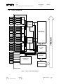
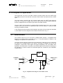
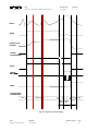
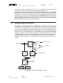
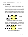
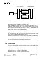
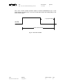
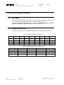
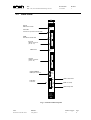
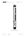
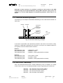
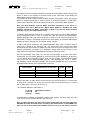
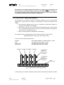
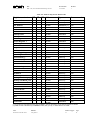
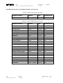
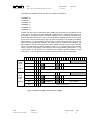
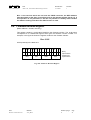
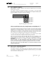
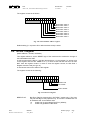
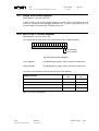
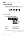
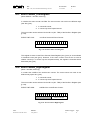
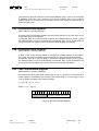
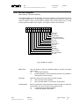
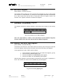
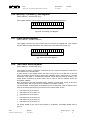
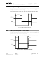
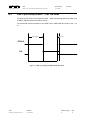


![[December] [2010] Oracle Part Number E51712-01](http://vs1.manualzilla.com/store/data/005705420_1-4b383e67b8ec6628c44005398bb7935f-150x150.png)