1
SAFETY PRECAUTIONS
(Read these instructions before using this equipment.)
Before using this product, please read this handbook and the relevant manuals carefully and pay full
attention to safety to handle the product correctly.
In this manual, the safety precautions are classified into two levels: "
WARNING" and "
CAUTION".
WARNING
Indicates that incorrect handling may cause hazardous conditions,
resulting in death or severe injury.
CAUTION
Indicates that incorrect handling may cause hazardous conditions,
resulting in minor or moderate injury or property damage.
Under some circumstances, failure to observe the precautions given under "
CAUTION" may lead to
serious consequences.
Observe the precautions of both levels because they are important for personal and system safety.
Make sure that the end users read this handbook and then keep the handbook in a safe place for future
reference.
A-1
[Design Precautions]
WARNING
● For the operation status of each station at communication error in each station, refer to the
respective manual for each station.
The communication error may result in an accident due to incorrect output or malfunction.
● For the operating status of each station after a communication failure, refer to relevant manuals for
the network. Erroneous outputs and malfunctions may lead to accidents.
Not doing so can cause an accident due to false output or malfunction.
● When using the notification function, the pager receiver may not be contacted due to the frequency
transmission status from the system setup environment and error on the receiver side.
To ensure the safety of the programmable controller system, install a call circuit with a lamp display
or buzzer sound.
● To prevent the malfunction of the programmable controller system due to harmful e-mails, take
preventive measures (such as antivirus measures) so that the mail server for this module does not
receive harmful e-mails.
● When performing the control of the programmable controller in operation (changing data) by
connecting a peripheral devices to the CPU module or personal computer, etc. to the intelligent
device module, configure an interlock circuit in a sequence program so the safety of the overall
system is always maintained.
Also when performing other controls of the programmable controller in operation (changing program
and operation status (status control)), read this manual carefully and confirm if the overall safety is
maintained.
Especially, when this control is performed to a remote programmable controller from an external
device, troubles that have occurred on the programmable controller side may not be able to
immediately be handled if there is a data communication error.
Define a troubleshooting agreement between external devices and the programmable controller
CPU for data communication error occurrences, as well as construct an interlock circuit in the
sequence program.
● When connecting a peripheral device to the CPU module or performing control of a programmable
controller which is being run through a BASIC program, configure an interlock circuit in the sequence
program so that the system overall is operating on the safe side at all times. Also before exercising
other control (program change, operating status change (status control)) on the running
programmable controller, read the manual carefully and fully confirm safety. Especially for the above
control on the remote programmable controller from, an immediate action may not be taken for
programmable controller trouble due to a data communication fault. In addition to configuring up the
interlock circuit in the sequence program, corrective and other actions to be taken as a system for
the occurrence of a data communication fault should be predetermined between and programmable
controller CPU.
A-2
[Design Precautions]
WARNING
● Do not write data into the "system area" of the buffer memory of intelligent function modules.
Also, do not use any "use prohibited" signals as an output signal to an intelligent function module
from the programmable controller CPU.
Writing data into the "system area" or outputting a signal for " use prohibited" may cause a
programmable controller system malfunction.
CAUTION
● Do not bunch the control wires or communication cables with the main circuit or power wires, or
install them close to each other.
They should be installed 100 mm (3.94 inch) or more from each other.
Not doing so could result in noise that may cause malfunction.
● When using the module while values, such as buffer memory set values, are registered in the Flash
ROM, do not turn off the power supply for the module loading station nor reset the programmable
controller CPU.
If the power supply for the module loading station is turned off or the programmable controller CPU is
reset while any values are registered, the data contents in the Flash ROM become inconsistent and
as a result the values must be set again in the buffer memory, etc. and reregistered to the Flash
ROM.
Also, this may cause failure and malfunction of the module.
● If a BASIC program is registered in the flash ROM in the module, do not power OFF or reset the
programmable controller CPU at the station where the module is installed during registration.
If it is performed during registration, the data contents in the flash ROM will be erratic and it will be
necessary to reset the setting values, etc. in the buffer memory and register them again in the flash
ROM. It could also cause the module to break down or malfunction.
● When changing the operating status of the programmable controller CPU (such as remote RUN/
STOP) from the external device, select "Always wait for OPEN (Communication possible at STOP time)"
for the "Initial timing" setting in the network parameter. The communication line will be closed when "Do
not wait for OPEN (Communications impossible at STOP time)" is selected and the remote STOP is
executed from the external device. Consequently, the programmable controller CPU cannot reopen the
communication line, and the external device cannot execute the remote RUN.
A-3
[Installation Precautions]
CAUTION
● Use the programmable controller in an environment that meets the general specifications contained
in the user's manual of the CPU module to use.
Using this programmable controller in an environment outside the range of the general specifications
may cause electric shock, fire, malfunction, and damage to or deterioration of the product.
● While pressing the installation lever located at the bottom of module, insert the module fixing tab into
the fixing hole in the base unit until it stops. Then, securely mount the module with the fixing hole as
a supporting point.
If the module is not installed properly, it may cause the module to malfunction, fail or fall off.
Secure the module with screws especially when it is used in an environment where constant
vibrations may occur.
● Tighten the screws within the range of specified torque.
If the screws are loose, it may cause the module to fallout, short circuits, or malfunction.
If the screws are tightened too much, it may cause damage to the screw and/or the module, resulting
in fallout, short circuits or malfunction.
● Before mounting/dismounting the module, be sure to shut off all phases of external power supply
used by the system.
Failure to do so may cause product damage.
● Do not directly touch the conductive area or electronic components of the module.
Doing so may cause malfunction or failure in the module.
A-4
[Wiring Precautions]
CAUTION
● When turning on the power and operating the module after installation and wiring are completed,
always attach the terminal cover that comes with the product.
There is a risk of electric shock if the terminal cover is not attached.
● Perform correct pressure-displacement, crimp-contact or soldering for external wire connections
using the tools specified by the manufactures.
Incorrect connection may cause short circuits, fire, or malfunction.
● Be sure to fix communication cables or power supply cables leading from the module by placing
them in the duct or clamping them.
Cables not placed in the duct or without clamping may hang or shift, allowing them to be accidentally
pulled, which may cause a module malfunction and cable damage.
● Shut off the external power supply (all phases) used in the system before connecting the AUI cable.
● When connecting a cable with connector to the module, connect the connector part to the module
securely.
● Attach connectors to the module securely.
● Before connecting the cables, check the type o f interface to be connected.
Connecting or erroneous wiring to the wrong interface may cause failure to the module and external
devices.
● Tighten the terminal screws within the range of specified torque.
If the terminal screws are loose, it may result in short circuits or malfunction.
If the screws are tightened too much, it may cause damage to the screw and/or the module, resulting
in fallout, short circuits or malfunction.
● When removing the communication cable or power supply cable from the module, do not pull the
cable. When removing the cable with a connector, hold the connector on the side that is connected
to the module.
When removing the cable connected to the terminal block, first loosen the screws on the part that is
connected to the terminal block.
Pulling the cable that is still connected to the module may cause malfunction or damage to the
module or cable.
● Be careful not to let foreign matters such as sawdust or wire chips get inside the module.
They may cause fires, failure or malfunction.
● The top surface of the module is covered with protective film to prevent foreign objects such as cable
offcuts from entering the module when wiring.
Do not remove this film until the wiring is complete.
Before operating the system, be sure to remove the film to provide adequate heat ventilation.
● Correctly solder coaxial cable connectors. Incomplete soldering may result in malfunction.
A-5
[Startup and Maintenance precautions]
CAUTION
● Do not disassemble or modify each module.
Doing so could cause failure, malfunction injury or fire.
● Before mounting/dismounting the module, be sure to shut off all phases of external power supply
used by the system.
Failure to do so may cause module failure or malfunctions.
● Do not install/remove the module to/from the base unit, or the terminal block to/from the module
more than 50 times after the first use of the product. (IEC 61131-2 compliant)
Failure to do so may cause malfunction.
● Do not touch the connector while the power is on.
Doing so may cause malfunction.
● Before cleaning up and retightening terminal screws and module fixing screws, be sure to shut off all
phases of external power supply used by the system.
Not doing so may cause failure or malfunction of the module.
If the screws are loose, it may cause the module to fallout, short circuits, or malfunction.
If the screws are tightened too much, it may cause damages to the screws and/or the module,
resulting in the module falling out, short circuits or malfunction.
● Always make sure to touch the grounded metal to discharge the electricity charged in the body, etc.,
before touching the module.
Failure to do so may cause a failure or malfunctions of the module.
[Operation Instructions]
CAUTION
● When performing the control of the programmable controller in operation (especially changing data,
program, and operation status (status control)) by connecting a personal computer, etc. to the
intelligent function module, read this manual carefully and confirm if the overall safety is maintained.
Failure to perform correct operations to change data, program, or the status may result in system
malfunction, machine damage, or an accident.
● When performing control (in particular, changing data, changing a program or changing the
operation status (status control)) of the programmable controller during operation using a BASIC
program, do so only after reading the user's manual thoroughly and taking adequate safety
precautions.
If there are errors when changing data, changing a program or in status control, it could result in
system malfunction, or cause mechanical damage or accidents.
[Disposal Precautions]
CAUTION
● When disposing of this product, treat it as industrial waste.
A-6
CONDITIONS OF USE FOR THE PRODUCT
(1) Mitsubishi programmable controller ("the PRODUCT") shall be used in conditions;
i) where any problem, fault or failure occurring in the PRODUCT, if any, shall not lead to any major
or serious accident; and
ii) where the backup and fail-safe function are systematically or automatically provided outside of
the PRODUCT for the case of any problem, fault or failure occurring in the PRODUCT.
(2) The PRODUCT has been designed and manufactured for the purpose of being used in general
industries.
MITSUBISHI SHALL HAVE NO RESPONSIBILITY OR LIABILITY (INCLUDING, BUT NOT
LIMITED TO ANY AND ALL RESPONSIBILITY OR LIABILITY BASED ON CONTRACT,
WARRANTY, TORT, PRODUCT LIABILITY) FOR ANY INJURY OR DEATH TO PERSONS OR
LOSS OR DAMAGE TO PROPERTY CAUSED BY the PRODUCT THAT ARE OPERATED OR
USED IN APPLICATION NOT INTENDED OR EXCLUDED BY INSTRUCTIONS, PRECAUTIONS,
OR WARNING CONTAINED IN MITSUBISHI'S USER, INSTRUCTION AND/OR SAFETY
MANUALS, TECHNICAL BULLETINS AND GUIDELINES FOR the PRODUCT.
("Prohibited Application")
Prohibited Applications include, but not limited to, the use of the PRODUCT in;
• Nuclear Power Plants and any other power plants operated by Power companies, and/or any
other cases in which the public could be affected if any problem or fault occurs in the PRODUCT.
• Railway companies or Public service purposes, and/or any other cases in which establishment of
a special quality assurance system is required by the Purchaser or End User.
• Aircraft or Aerospace, Medical applications, Train equipment, transport equipment such as
Elevator and Escalator, Incineration and Fuel devices, Vehicles, Manned transportation,
Equipment for Recreation and Amusement, and Safety devices, handling of Nuclear or
Hazardous Materials or Chemicals, Mining and Drilling, and/or other applications where there is a
significant risk of injury to the public or property.
Notwithstanding the above, restrictions Mitsubishi may in its sole discretion, authorize use of the
PRODUCT in one or more of the Prohibited Applications, provided that the usage of the PRODUCT
is limited only for the specific applications agreed to by Mitsubishi and provided further that no
special quality assurance or fail-safe, redundant or other safety features which exceed the general
specifications of the PRODUCTs are required. For details, please contact the Mitsubishi
representative in your region.
A-7
REVISIONS
* The handbook number is given on the bottom left of the back cover.
Print Date
* Handbook Number
Apr., 2005
L(NA)-08050ENG-A
Oct., 2005
L(NA)-08050ENG-B
Revision
First edition
Addition
Appendix 1
Partial correction
Contents, Chapter 1, Section 3.1, Section 3.2.1, Section 3.3, Section 3.4,
Section 3.5, Section 3.6.1, Section 3.6.2, Section 4.1, Section 4.2,
Appendix 1→Appendix 2
May, 2006
L(NA)-08050ENG-C
Addition
Chapter 4
Partial correction
Contents, Chapter 1, Section 2.1, Section 2.7, Section 3.1,
Chapter 4→Chapter 5, Appendix 1, Appendix 2
Mar., 2008
L(NA)-08050ENG-D
Partial correction
Term revision (whole), Appendix 2.1
Nov., 2012
L(NA)-08050ENG-E
Model Addition
MELSEC-AnS/QnAS series
Addition
Section 1.2, Appendix 2
Partial correction
SAFETY PRECAUTIONS, Chapter 1 to 9, Appendix
Japanese Handbook Version L-08049-F
This handbook confers no industrial property rights or any rights of any other kind, nor does it confer any patent licenses.
Mitsubishi Electric Corporation cannot be held responsible for any problems involving industrial property rights which may
occur as a result of using the contents noted in this handbook.
© 2005 MITSUBISHI ELECTRIC CORPORATION
A-8
CONTENTS
SAFETY PRECAUTIONS ................................................................................................................................A - 1
CONDITIONS OF USE FOR THE PRODUCT .................................................................................................A - 7
REVISIONS ......................................................................................................................................................A - 8
CONTENTS .....................................................................................................................................................A - 9
GENERIC TERMS AND ABBREVIATIONS ................................................................................................... A - 11
CHAPTER 1 INTRODUCTION
1 - 1 to 1 - 5
1.1
Replacement of Modules Introduced in This Handbook .................................................................. 1 - 1
1.2
Basic Precautions ............................................................................................................................ 1 - 5
CHAPTER 2 SERIAL COMMUNICATION MODULE REPLACEMENT
2 - 1 to 2 - 35
2.1
List of Serial Communication Modules to be Replaced ................................................................... 2 - 1
2.2
Performance Specifications Comparison ......................................................................................... 2 - 2
2.2.1
2.2.2
Module performance comparison ............................................................................................. 2 - 2
Cable specifications comparison .............................................................................................. 2 - 9
2.3
Function Comparison ..................................................................................................................... 2 - 13
2.4
Switch Setting Comparison ............................................................................................................ 2 - 15
2.5
Program Comparison ..................................................................................................................... 2 - 20
2.5.1
2.5.2
2.6
I/O signal ................................................................................................................................ 2 - 20
Buffer memory ........................................................................................................................ 2 - 23
Reuse of Existing Programs .......................................................................................................... 2 - 26
2.6.1
2.6.2
Reuse of A/AnS series programs ........................................................................................... 2 - 26
Reuse of QnA/QnAS series programs .................................................................................... 2 - 28
2.7
Other Precaution ............................................................................................................................ 2 - 29
2.8
Program Examples ........................................................................................................................ 2 - 30
CHAPTER 3 ETHERNET INTERFACE MODULE REPLACEMENT
3 - 1 to 3 - 35
3.1
List of Ethernet Interface Modules to be Replaced .......................................................................... 3 - 1
3.2
Performance Specifications Comparison ......................................................................................... 3 - 2
3.2.1
3.2.2
Module performance comparison ............................................................................................. 3 - 2
Cable specifications comparison .............................................................................................. 3 - 6
3.3
Function Comparison ....................................................................................................................... 3 - 7
3.4
Switch Setting Comparison ............................................................................................................ 3 - 12
3.5
Parameter Comparison .................................................................................................................. 3 - 14
3.6
Program Comparison ..................................................................................................................... 3 - 15
3.6.1
3.6.2
3.7
I/O signal ................................................................................................................................ 3 - 15
Buffer memory ........................................................................................................................ 3 - 19
Reuse of Existing Programs .......................................................................................................... 3 - 22
A-9
3.8
Other Precaution ............................................................................................................................ 3 - 24
3.9
Program Examples ........................................................................................................................ 3 - 25
3.9.1
3.9.2
3.9.3
Initial processing ..................................................................................................................... 3 - 26
Open/close processing ........................................................................................................... 3 - 29
Communication using fixed buffer .......................................................................................... 3 - 33
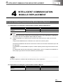
CHAPTER 4 INTELLIGENT COMMUNICATION MODULE REPLACEMENT 4 - 1 to 4 - 27
4.1
List of Intelligent Communication Modules to be Replaced ............................................................. 4 - 1
4.2
Performance Specifications Comparison ......................................................................................... 4 - 2
4.2.1
4.2.2
Module performance comparison ............................................................................................. 4 - 2
Cable specifications comparison .............................................................................................. 4 - 5
4.3
Function Comparison ....................................................................................................................... 4 - 7
4.4
Switch Setting .................................................................................................................................. 4 - 9
4.5
Program Comparison ..................................................................................................................... 4 - 15
4.5.1
4.5.2
4.6
I/O signal ................................................................................................................................ 4 - 15
Buffer memory ........................................................................................................................ 4 - 21
Reuse of Existing Programs .......................................................................................................... 4 - 22
4.6.1
4.6.2
4.6.3
Replacement of intelligent communication module AD51H-S3 .............................................. 4 - 22
Replacement of intelligent communication module A1SD51S ................................................ 4 - 24
Replacement of intelligent communication module AD51-S3 ................................................. 4 - 27
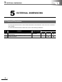
CHAPTER 5 EXTERNAL DIMENSIONS
5.1
5 - 1 to 5 - 2
External Dimensions ........................................................................................................................ 5 - 1
APPENDICES
App - 1 to App - 9
Appendix 1 Spare Parts Storage ..........................................................................................................App - 1
Appendix 2 Procedure for Replacing the A1SD51S with the QD51(-R24) ...........................................App - 2
Appendix 3 Relevant Manuals ..............................................................................................................App - 6
Appendix 3.1
Appendix 3.2
Appendix 3.3
Appendix 3.4
A - 10
Replacement Handbooks ...........................................................................................App - 6
A/AnS series ...............................................................................................................App - 8
QnA/QnAS series .......................................................................................................App - 8
Q series ......................................................................................................................App - 8
GENERIC TERMS AND ABBREVIATIONS
Unless otherwise specified, this handbook uses the following generic terms and abbreviations.
Generic term/abbreviation
Series
A series
AnS series
A/AnS series
QnA series
QnAS series
QnA/QnAS series
A/AnS/QnA/QnAS series
Q series
CPU module type
CPU module
Basic model QCPU
High Performance model
QCPU
Process CPU
Redundant CPU
Description
Abbreviation for large types of Mitsubishi MELSEC-A series programmable controllers
Abbreviation for compact types of Mitsubishi MELSEC-A series programmable controllers
Generic term for A series and AnS series
Abbreviation for large types of Mitsubishi MELSEC-QnA series programmable controllers
Abbreviation for compact types of Mitsubishi MELSEC-QnA series programmable controllers
Generic term for QnA series and QnAS series
Generic term for A series, AnS series, QnA series, and QnAS series
Abbreviation for Mitsubishi MELSEC-Q series programmable controllers
Generic term for A series, AnS series, QnA series, QnAS series, and Q series CPU modules
Generic term for the Q00JCPU, Q00CPU, and Q01CPU
Generic term for the Q02CPU, Q02HCPU, Q06HCPU, Q12HCPU, and Q25HCPU
* This handbook mainly explains about the Q02CPU, Q02HCPU, Q06HCPU, and Q12HCPU.
Generic term for the Q02PHCPU, Q06PHCPU, Q12PHCPU, and Q25PHCPU
Generic term for the Q12PRHCPU and Q25PRHCPU
Generic term for the Q00UJCPU, Q00UCPU, Q01UCPU, Q02UCPU, Q03UDCPU,
Q04UDHCPU, Q06UDHCPU, Q10UDHCPU, Q13UDHCPU, Q20UDHCPU, Q26UDHCPU,
Q03UDECPU, Q04UDEHCPU, Q06UDEHCPU, Q10UDEHCPU, Q13UDEHCPU,
Universal model QCPU
Q20UDEHCPU, Q26UDEHCPU, Q50UDEHCPU, and Q100UDEHCPU
*
This handbook mainly explains about the Q00UJCPU, Q00UCPU, Q01UCPU, Q02UCPU,
Q03UDCPU, Q04UDHCPU, and Q06UDHCPU, which can replace the AnS/QnAS series.
The specifications and functions of the Q10UDEHCPU to Q100UDEHCPU are the same as those of
the modules described above, although the program and memory capacities increase.
CPU module model
ACPU
AnSCPU
A/AnSCPU
AnNCPU
AnACPU
AnUCPU
AnN/AnACPU
AnN/AnA/AnSCPU
QnACPU
QnASCPU
QnA/QnASCPU
A/AnS/QnA/QnASCPU
QCPU
Generic term for MELSEC-A series programmable controller CPUs
Generic term for MELSEC-AnS series programmable controller CPUs
Generic term for MELSEC-A series and MELSEC-AnS series programmable controller CPUs
Generic term for the A1NCPU, A1NCPUP21/R21, A1NCPUP21-S3, A2NCPU, A2NCPU-S1,
A2NCPUP21/R21, A2NCPUP21/R21-S1, A2NCPUP21-S3(S4), A3NCPU, A3NCPUP21/R21,
and A3NCPUP21-S3
Generic term for the A2ACPU, A2ACPU-S1, A3ACPU, A2ACPUP21/R21, A2ACPUP21/R21S1, and A3ACPUP21/R21
Generic term for the A2UCPU, A2UCPU-S1, A3UCPU, A4UCPU, A2USCPU, A2USCPU-S1,
and A2USHCPU-S1
Generic term for the AnNCPU and AnACPU
Generic term for the AnNCPU, AnACPU, and AnSCPU
Generic term for MELSEC-QnA series programmable controller CPUs
Generic term for MELSEC-QnAS series programmable controller CPUs
Generic term for MELSEC-QnA series and MELSEC-QnAS series programmable controller
CPUs
Generic term for A series, AnS series, QnA series, and QnAS series programmable controller
CPUs
Generic term for MELSEC-Q series programmable controller CPUs
A - 11
1
INTRODUCTION
1
INTRODUCTION
1
1.1 Replacement of Modules Introduced in This Handbook
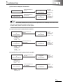
This section outlines the replacement of the following communication modules.
•
•
•
•
•
A/AnS series computer link module
QnA/QnAS series serial communication module
A/AnS series Ethernet interface module
QnA/QnAS series Ethernet interface module
A/AnS intelligent communication module
: Refer to CHAPTER 2.
: Refer to CHAPTER 2.
: Refer to CHAPTER 3.
: Refer to CHAPTER 3.
: Refer to CHAPTER 4.
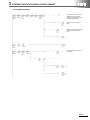
(1) Replacement of A/AnS series computer link modules and QnA/QnAS series serial
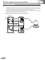
communication modules
(a) A series computer link module
Communications via RS-232
QJ71C24N
or
QJ71C24N-R2
QJ71C24N
RS-232
:1ch
RS-422/485:1ch
QJ71C24N-R2
RS-232
:2ch
QJ71C24N
or
QJ71C24N-R4
QJ71C24N
RS-232
:1ch
RS-422/485 :1ch
QJ71C24N-R4
RS-422/485 :2ch
AJ71UC24
AJ71UC24
RS-232
:1ch
RS-422/485 :1ch
Communications via RS-422/485
Point
Q series communication modules do not have a function equivalent to the multidrop link function of the
A series communication module AJ71UC24.
Configure other systems such as a CC-Link system.
1-1
1
INTRODUCTION
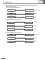
(b) AnS series computer link module
A1SJ71UC24
RS-232
Communications via
RS-232
:1ch
A1SJ71UC24-R4
Communications via
RS-422/485
RS-422/485:1ch
QJ71C24N
or
QJ71C24N-R2
QJ71C24N
RS-232
:1ch
RS-422/485 :1ch
QJ71C24N-R2
RS-232
:2ch
QJ71C24N
or
QJ71C24N-R4
QJ71C24N
RS-232
:1ch
RS-422/485 :1ch
QJ71C24N-R4
RS-422/485 :2ch
Point
Q series communication modules do not have a function equivalent to the multidrop link function of the
AnS series communication module A1SJ71UC24.
Consider other systems such as a CC-Link system.
(c) QnA series serial communication module
AJ71QC24N
or
AJ71QC24N-R2
Communications via
RS-232
QJ71C24N
or
QJ71C24N-R2
QJ71C24N
RS-232
:1ch
RS-422/485:1ch
QJ71C24N-R2
RS-232
:2ch
QJ71C24N
or
QJ71C24N-R4
QJ71C24N
RS-232
:1ch
RS-422/485 :1ch
QJ71C24N-R4
RS-422/485 :2ch
QJ71C24N
or
QJ71C24N-R2
QJ71C24N
RS-232
:1ch
RS-422/485 :1ch
QJ71C24N-R2
RS-232
:2ch
QJ71C24N
or
QJ71C24N-R4
QJ71C24N
RS-232
:1ch
RS-422/485 :1ch
QJ71C24N-R4
RS-422/485 :2ch
AJ71QC24N
RS-232
:1ch
RS-422/485 :1ch
AJ71QC24N-R2
RS-232
:2ch
AJ71QC24N
or
AJ71QC24N-R4
Communications via
RS-422/485
AJ71QC24N
RS-232
:1ch
RS-422/485 :1ch
AJ71QC24N-R4
RS-422
:1ch
RS-422/485 :1ch
(d) QnAS series serial communication module
A1SJ71QC24N1
or
A1SJ71QC24N1-R2
Communications via
RS-232
A1SJ71QC24N1
RS-232
:1ch
RS-422/485 :1ch
A1SJ71QC24N1-R2
RS-232
:2ch
A1SJ71QC24N1
Communications via
RS-422/485
A1SJ71QC24N1
RS-232
:1ch
RS-422/485 :1ch
1-2
1
INTRODUCTION
(2) Replacement of A/AnS series Ethernet interface modules and QnA/QnAS series
Ethernet interface modules
(a) A series Ethernet interface module
AJ71E71N3-T
Communications via 10BASE-T
QJ71E71-100
QJ71E71-100
10BASE-T/100BASE-TX:1ch
AJ71E71N3-T
10BASE-T:1ch
AJ71E71N-B5
Communications via 10BASE5
QJ71E71-B5
QJ71E71-B5
10BASE5:1ch
QJ71E71-B2
QJ71E71-B2
10BASE2:1ch
AJ71E71N-B5
10BASE5 :1ch
AJ71E71N-B2
Communications via 10BASE2
AJ71E71N-B2
10BASE2 :1ch
(b) AnS series Ethernet interface module
A1SJ71E71N3-T
Communications via 10BASE-T
QJ71E71-100
QJ71E71-100
10BASE-T/100BASE-TX :1ch
QJ71E71-B5
QJ71E71-B5
10BASE5 :1ch
QJ71E71-B2
QJ71E71-B2
10BASE2 :1ch
A1SJ71E71N3-T
10BASE-T :1ch
A1SJ71E71N-B5
Communications via 10BASE5
A1SJ71E71N-B5
10BASE5 :1ch
A1SJ71E71N-B2
Communications via 10BASE2
A1SJ71E71N-B2
10BASE2 :1ch
(c) QnA series Ethernet interface module
AJ71QE71N3-T
Communications via 10BASE-T
QJ71E71-100
QJ71E71-100
10BASE-T/100BASE-TX:1ch
QJ71E71-B5
QJ71E71-B5
10BASE5:1ch
QJ71E71-B2
QJ71E71-B2
10BASE2:1ch
AJ71QE71N3-T
10BASE-T:1ch
AJ71QE71N-B5
Communications via 10BASE5
AJ71QE71N-B5
10BASE5 :1ch
AJ71QE71N-B2
AJ71QE71N-B2
10BASE2 :1ch
1-3
Communications via 10BASE2
1
INTRODUCTION
(d) QnAS series Ethernet interface module
A1SJ71QE71N3-T
Communications via 10BASE-T
QJ71E71-100
QJ71E71-100
10BASE-T/100BASE-TX :1ch
Communications via 10BASE5
QJ71E71-B5
QJ71E71-B5
10BASE5 :1ch
Communications via 10BASE2
QJ71E71-B2
QJ71E71-B2
10BASE2 :1ch
A1SJ71QE71N3-T
10BASE-T :1ch
A1SJ71QE71N-B5
A1SJ71QE71N-B5
10BASE5 :1ch
A1SJ71QE71N-B2
A1SJ71QE71N-B2
10BASE2 :1ch
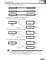
(3) Replacement of intelligent communication modules
(a) Intelligent communication module AD51H-S3
Communications via
RS-232
AD51H-S3
QD51
or
QD51-R24
AD51H-S3
RS-232:2ch
RS-422:1ch
Parallel:1ch
QD51
RS-232
:2ch
QD51-R24
RS-232
:1ch
RS-422/485:1ch
QD51-R24
Communications via
RS-422
QD51-R24
RS-232
:1ch
RS-422/485:1ch
(b) Intelligent communication module AD51-S3
Communications via
RS-232
AD51-S3
QD51
or
QD51-R24
QD51
RS-232
:2ch
QD51-R24
RS-232
:1ch
RS-422/485:1ch
AD51-S3
RS-232:2ch
RS-422:2ch
QD51-R24
Communications via
RS-422
QD51-R24
RS-232
:1ch
RS-422/485:1ch
(c) Intelligent communication module A1SD51S
Communications via
RS-232
A1SD51S
QD51
or
QD51-R24
QD51
RS-232
:2ch
QD51-R24
RS-232
:1ch
RS-422/485:1ch
A1SD51S3
RS-232:2ch
RS-422:1ch
Communications via
RS-422/485
QD51-R24
QD51-R24
RS-232
:1ch
RS-422/485:1ch
Point
• Q series intelligent communication modules do not have a parallel interface. Please consider
changing the external devices to RS-232/RS-422 interface devices.
• The BASIC program of the AD51-S3 is incompatible with that of the QD51/QD51-R24. Analyze
the existing program to create a program with AD51H-BASIC.
1-4
1
INTRODUCTION
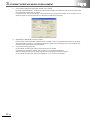
1.2 Basic Precautions
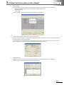
(1) When using the sequence program of the A/AnS/QnA/QnAS series on the Q series
The sequence program of the A/AnS/QnA/QnAS series can be converted to be used on the Q series on
GX Developer. (On GX Works2, the sequence program of the A/Ans/QnA/QnAS series cannot be
converted for the Q series.)
To convert the sequence program of the A/AnS/QnA/QnAS series to be used on the Q series, use GX
Developer.
(2) When creating a new sequence program for the Q series
A sequence program can be created for the Q series on GX Developer and GX Works2.
1-5
2
SERIAL COMMUNICATION MODULE REPLACEMENT
2
SERIAL COMMUNICATION MODULE
REPLACEMENT
2
2.1 List of Serial Communication Modules to be Replaced
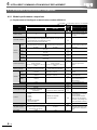
(1) Transition of the A series to Q series
Model to be discontinued
AJ71UC24
Alternative model
QJ71C24N
QJ71C24N-R2
QJ71C24N-R4
Remarks
RS-232:1ch, RS-422/485:1ch
RS-232:2ch, RS-422/485:none
RS-232:none, RS-422/485:2ch
(2) Transition of the AnS series to Q series
Model to be discontinued
A1SJ71UC24-R2
A1SJ71UC24-R4
Alternative model
QJ71C24N
QJ71C24N-R2
QJ71C24N
QJ71C24N-R4
Remarks
RS-232:1ch, RS-422/485:1ch
RS-232:2ch, RS-422/485:none
RS-232:1ch, RS-422/485:1ch
RS-232:none, RS-422/485:2ch
(3) Transition of the QnA series to Q series
Model to be discontinued
AJ71QC24N
AJ71QC24N-R2
AJ71QC24N-R4
Alternative model
QJ71C24N
QJ71C24N-R2
QJ71C24N-R4
Remarks
RS-232:1ch, RS-422/485:1ch
RS-232:2ch, RS-422/485:none
RS-232:none, RS-422/485:2ch
(4) Transition of the QnAS series to Q series
Model to be discontinued
A1SJ71QC24N1
A1SJ71QC24N1-R2
Alternative model
QJ71C24N
QJ71C24N-R2
Remarks
RS-232:1ch, RS-422/485:1ch
RS-232:2ch, RS-422/485:none
2-1
2
SERIAL COMMUNICATION MODULE REPLACEMENT
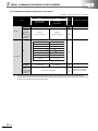
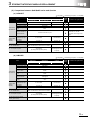
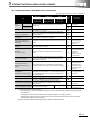
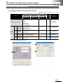
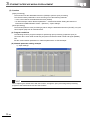
2.2 Performance Specifications Comparison
2.2.1 Module performance comparison
(1) Comparison between A series and Q series
:Compatible,
Specifications
Item
RS-232
Interface
RS-422/485
Communication
using dedicated
Communication protocol*1
method
Non-procedural/
bidirectional
communication
Synchronization method
Transmission speed
Access cycle
Error
detection
Q series
AJ71UC24
QJ71C24N*2
RS-232 compliant
(D-Sub 25P)
RS-232 compliant
(D-Sub 9P)
The connector on the
connection cable must be
changed.
RS-422/485 compliant
RS-422/485 compliant
(2-piece terminal block)
Wiring must be changed.
Half-duplex communication
Full duplex communication (1:1 connection)/
Half-duplex communication (1:n, m:n connection)
Start stop synchronization (asynchronous method)
300 to 19200 bps
50 to 230400 bps
Line
configuration
(connection)
7 or 8
Parity bit
1 (vertical parity)/none
Stop bit
1 or 2
Communication
using dedicated
protocol
One request is processed when the mounted station programmable
controller CPU executes END processing.
Non-procedural/
bidirectional
communication
Transmission can be executed at each send request,
and reception is available at all times.
Parity check
Performed (odd/even)/none
Sum check
Performed (MC protocol/Bidirectional)/none
RS-232
RS-422/485
DTR/DSR (ER/DR) control
Available
N/A
CD signal control
Available
N/A
DC1/DC3 (Xon/Xoff) control
DC2/DC4 control
Available
Available
RS-232
1:1
RS-422/485
1 :1, 1 : n, m : n
(n:max. 32, m+n:max.32)
Communication
using dedicated
protocol
1:1, 1:n, m:n
(n:max.32, m+n:max.32)
Line
configuration
Non-procedural
(data
communication
communication)
Bidirectional
communication
Transmission
distance
1
Data bit
Transmission control
No. of E2PROM writes
No. of flash ROM writes
No. of occupied I/O points
1:1, 1:n, n:1 (n:max.32)
1:1, 1:n (n:max.32)
For details on linked operation
between interfaces, refer to
the manual.
1:1
RS-232
RS-422/485
CompatPrecautions for replacement
ibility
A series
Start bit
Data format
:Partial change required, ×:Incompatible
Max.15m
Max.500m
(overall distance)
Max.1200m
(overall distance)
Max. 100,000 times on same
area in E2PROM
Max. 100,000 times on same
area in flash ROM
32 points/slot
(I/O assignment: special 32
points)
32 points/slot
(I/O assignment: intelli. 32
points)
*1
On the Q series, this is called "MELSEC communication protocol" (abbrev. "MC protocol").
*2
When the AJ71UC24 uses only the RS-232 channel, it can be replaced with the QJ71C24N-R2.
When the AJ71UC24 uses only the RS-422 channel, it can be replaced with the QJ71C24N-R4.
2-2
2
SERIAL COMMUNICATION MODULE REPLACEMENT
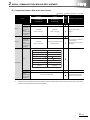
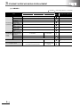
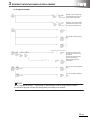
(2) Comparison between AnS series and Q series
(a) A1SJ71UC24-R2
:Compatible,
:Partial change required, ×:Incompatible
Specifications
Item
AnS series
Q series
A1SJ71UC24-R2
QJ71C24N
QJ71C24N-R2
RS-232
QJ71C24N
:1ch
QJ71C24N-R2 :2ch
RS-232 compliant (D-Sub 9P)
Interface
RS-422/485
CompatPrecautions for replacement
ibility
RS-422/485 compliant
(2-piece terminal block)
-
Communication
using dedicated
-
QJ71C24N
:1ch
QJ71C24N-R2 :none
Half-duplex communication
protocol*1
Communication
method
Non-procedural/
bidirectional
communication
Synchronization method
Transmission speed
Start stop synchronization (asynchronous method)
300 to 19200 bps
50 to 230400 bps
Start bit
Data format
Access cycle
Error
detection
1
Data bit
7 or 8
Parity bit
1 (vertical parity)/none
Stop bit
1 or 2
Communication
using dedicated
protocol
One request is processed when the mounted station programmable
controller CPU executes END processing.
Non-procedural/
bidirectional
communication
Transmission can be executed at each send request,
and reception is available at all times.
Parity check
Performed (odd/even)/none
Sum check
Performed (MC protocol/Bidirectional)/none
Transmission control
Line
configuration
(connection)
RS-232
RS-422/485
DTR/DSR (ER/DR) control
Available
N/A
CD signal control
Available
N/A
DC1/DC3 (Xon/Xoff) control
DC2/DC4 control
Available
Available
RS-232
RS-422/485
1:1
Line
configuration
Non-procedural
(data
communication
communication)
Bidirectional
communication
1:1, 1:n, m:n
(n:max.32, m+n:max.32)
1:1, 1:n (n:max.32)
RS-422/485
No. of occupied I/O points
1:1, 1:n, n:1 (n:max.32)
For details on linked operation
between interfaces, refer to
the manual.
1:1
RS-232
No. of E2PROM writes
No. of flash ROM writes
*1
1 :1, 1 : n, m : n
(n:max. 32, m+n:max.32)
-
Communication
using dedicated
protocol
Transmission
distance
Full duplex communication (1:1
connection)/
Half-duplex communication (1:n,
m:n connection)
Full duplex communication (1:1
connection)
Max.15m
Max. 100,000 times on same
Max.1200m
(overall distance)
area in E2PROM
Max. 100,000 times on same
area in flash ROM
32 points/slot
(I/O assignment: special 32
points)
32 points/slot
(I/O assignment: intelli. 32
points)
On the Q series, this is called "MELSEC communication protocol" (abbrev. "MC protocol").
2-3
2
SERIAL COMMUNICATION MODULE REPLACEMENT
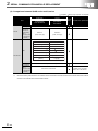
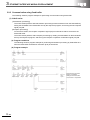
(b) A1SJ71UC24-R4
:Compatible,
:Partial change required, ×:Incompatible
Specifications
Item
RS-232
AnS series
Q series
A1SJ71UC24-R4
QJ71C24N
QJ71C24N-R4
-
RS-232 compliant
(D-Sub 9P)
RS-422/485 compliant
RS-422/485 compliant
(2-piece terminal block)
Interface
RS-422/485
Communication
using dedicated
Communication protocol*1
method
Non-procedural/
bidirectional
communication
Synchronization method
Transmission speed
Access cycle
Error
detection
Line
configuration
(connection)
50 to 230400 bps
Transmission
distance
7 or 8
Stop bit
1 or 2
Communication
using dedicated
protocol
One request is processed when the mounted station programmable
controller CPU executes END processing.
Non-procedural/
bidirectional
communication
Transmission can be executed at each send request,
and reception is available at all times.
Parity check
Performed (odd/even)/none
Sum check
Performed (MC protocol/Bidirectional)/none
RS-422/485
DTR/DSR (ER/DR) control
Available
N/A
CD signal control
Available
N/A
DC1/DC3 (Xon/Xoff) control
DC2/DC4 control
Available
Available
-
1:1
RS-422/485
Communication
using dedicated
protocol
1:1, 1:n, m:n
(n:max.32, m+n:max.32)
RS-232
RS-422/485
No. of occupied I/O points
2-4
RS-232
1 :1, 1 : n, m : n
(n:max. 32, m+n:max.32)
No. of E2PROM writes
No. of flash ROM writes
*1
1
1 (vertical parity)/none
Line
configuration
Non-procedural
(data
communication
communication)
Bidirectional
communication
QJ71C24N
:1ch
QJ71C24N-R4 :2ch
The wiring must be changed.
Start stop synchronization (asynchronous method)
300 to 19200 bps
Parity bit
RS-232
QJ71C24N
:1ch
QJ71C24N-R4 :none
Full duplex communication (1:1 connection)/
Half-duplex communication (1:n, m:n connection)
Data bit
Transmission control
-
Half-duplex communication
Start bit
Data format
CompatPrecautions for replacement
ibility
1:1, 1:n, n:1 (n:max.32)
1:1, 1:n (n:max.32)
1:1
-
Max.15m
Max.500m
(overall distance)
Max.1200m
(overall distance)
Max. 100,000 times on same
area in E2PROM
Max. 100,000 times on same
area in flash ROM
32 points/slot
(I/O assignment: special 32
points)
32 points/slot
(I/O assignment: intelli. 32
points)
On the Q series, this is called "MELSEC communication protocol" (abbrev. "MC protocol").
For details on linked operation
between interfaces, refer to
the manual.
2
SERIAL COMMUNICATION MODULE REPLACEMENT
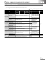
(3) Comparison between QnA series and Q series
:Compatible,
:Partial change required, ×:Incompatible
Specifications
QnA series
Q series
AJ71QC24N
AJ71QC24N-R2
AJ71QC24N-R4
QJ71C24N
QJ71C24N-R2
QJ71C24N-R4
RS-232
RS-232 compliant
(D-Sub 25P)
RS-232 compliant
(D-Sub 9P)
RS-422
RS-422 compliant
(D-Sub 25P)
RS-422/485 compliant
(2-piece plug-in connector socket
block)
RS-422/485 compliant
(2-piece terminal block)
RS-422/485 compliant
(2-piece terminal block)
(2-piece plug-in connector socket
block)
Item
RS-422/485
Interface
Communication
using dedicated
CompatPrecautions for replacement
ibility
The connector on the
connection cable must be
changed.
Wiring must be changed.
Half-duplex communication
protocol*1
Non-procedural
protocol
communication
Full duplex communication/Half-duplex communication
Bidirectional
protocol
communication
Full duplex communication/Half-duplex communication
Synchronization method
Transmission speed
Start stop synchronization (asynchronous method)
300 to 230400 bps
Start bit
Data format
Data bit
7 or 8
Parity bit
1 (vertical parity)/none
Stop bit
1 or 2
Communication
using dedicated
protocol
Access cycle
Non-procedural
protocol
communication
Bidirectional
protocol
communication
Error
detection
50 to 230400 bps
1
Processing when the mounted station programmable controller CPU
performs END processing
Transmission can be executed at each send request,
and reception is available at all times.
Parity check
Performed (odd/even)/none
Sum check
Performed/none
RS-232
Transmission control
Select at parameter/user frame.
RS-422 RS-422/485
DTR/DSR (ER/DR) control
Available Available
N/A
RS/CS control
Available
N/A
N/A
CD signal control
Available
N/A
N/A
DC1/DC3 (Xon/Xoff) control Available Available
DC2/DC4 control
Line
configuration
(connection)
RS-232
RS-422
RS-422/485
Available
1:1
1:1
-
1:1, 1:n, m:n
(n:max.32, m+n:max.32)
1:1, 1:n, n:1, m:n
(n:max.32, m+n:max.32)
The Q series does not have the
RS-422 interface.
Transmission control must be
changed to the transmission
control of the interface to be
used.
The Q series does not have the
RS-422 interface.
The interface to be used must
be changed.
(Continued on next page)
2-5
2
SERIAL COMMUNICATION MODULE REPLACEMENT
:Compatible,
:Partial change required, ×:Incompatible
Specifications
Item
Communication
using dedicated
protocol
line
Non-procedural
configuration
protocol
(data
communication
communication)
Bidirectional
protocol
communication
QnA series
Q series
AJ71QC24N
AJ71QC24N-R2
AJ71QC24N-R4
QJ71C24N
QJ71C24N-R2
QJ71C24N-R4
1:1, 1:n, m:n
(n:max.32, m+n:max.32)
1:1, 1:n (n:max.32)
RS-422
RS-422/485
E2PROM
No. of
writes
No. of flash ROM writes
No. of occupied I/O points
*1
2-6
1:1, 1:n, n:1 (n:max.32)
For details on linked operation
between interfaces, refer to
the manual.
-
The Q series does not have
the RS-422 interface.
The interface to be used must
be changed.
1:1
RS-232
Transmission
distance
CompatPrecautions for replacement
ibility
Max.15m
Max.1200m
Max.1200m (overall distance)
Max. 100,000 times on same
area in E2PROM
32 points/slot
(I/O assignment: special 32
points)
Max. 100,000 times on same
area in flash ROM
32 points/slot
(I/O assignment: intelli. 32 points)
On the Q series, this is called "MELSEC communication protocol" (abbrev. "MC protocol").
2
SERIAL COMMUNICATION MODULE REPLACEMENT
(4) Comparison between QnAS series and Q series
:Compatible,
:Partial change required, ×:Incompatible
Specifications
Item
RS-232
RS-422/485
Interface
Communication
using dedicated
QnAS series
Q series
A1SJ71QC24N1
AJ71QC24N1-R2
QJ71C24N
QJ71C24N-R2
QJ71C24N-R4
QJ71C24N : 1ch
QJ71C24N-R2: 2ch
QJ71C24N-R4: none
RS-232 compliant (D-Sub 9P)
RS-422/485 compliant
(2-piece terminal block)
(2-piece plug-in connector socket
block)
RS-422/485 compliant
(2-piece terminal block)
CompatPrecautions for replacement
ibility
QJ71C24N : 1ch
QJ71C24N-R2: none
QJ71C24N-R4: 2ch
Wiring must be changed.
Half-duplex communication
protocol*1
Non-procedural
protocol
communication
Full duplex communication/Half-duplex communication
Bidirectional
protocol
communication
Full duplex communication/Half-duplex communication
Synchronization method
Transmission speed
Start stop synchronization (asynchronous method)
300 to 115200 bps
50 to 230400 bps
Start bit
Data format
Data bit
7 or 8
Parity bit
1 (vertical parity)/none
Stop bit
1 or 2
Communication
using dedicated
protocol
Access cycle
Non-procedural
protocol
communication
Bidirectional
protocol
communication
Error
detection
1
Processing when the mounted station programmable controller CPU
performs END processing
Transmission can be executed at each send request,
and reception is available at all times.
Parity check
Performed (odd/even)/none
Sum check
Performed/none
Select at parameter/user frame.
RS-232 RS-422/485
Transmission control
DTR/DSR (ER/DR) control
Available
N/A
RS/CS control
Available
N/A
CD signal control
Available
N/A
DC1/DC3 (Xon/Xoff) control
Available
DC2/DC4 control
Line
configuration
(connection)
RS-232
RS-422/485
Available
1:1
1:1, 1:n, m:n
(n:max.32, m+n:max.32)
1:1, 1:n, n:1, m:n
(n:max.32, m+n:max.32)
(Continued on next page)
2-7
2
SERIAL COMMUNICATION MODULE REPLACEMENT
:Compatible,
:Partial change required, ×:Incompatible
Specifications
Item
Communication
using dedicated
protocol
line
Non-procedural
configuration
protocol
(data
communication
communication)
Bidirectional
protocol
communication
Transmission
distance
RS-422/485
No. of occupied I/O points
2-8
QJ71C24N
QJ71C24N-R2
QJ71C24N-R4
CompatPrecautions for replacement
ibility
1:1, 1:n, m:n
(n:max.32, m+n:max.32)
1:1, 1:n (n:max.32)
1:1, 1:n, n:1 (n:max.32)
1:1
RS-232
No. of E2PROM writes
No. of flash ROM writes
*1
AJ71QC24N
AJ71QC24N-R2
AJ71QC24N-R4
Max.15m
Max.1200m (overall distance)
Max. 100,000 times on same
area in E2PROM
32 points/slot
(I/O assignment: special 32
points)
Max. 100,000 times on same
area in flash ROM
32 points/slot
(I/O assignment: intelli. 32 points)
On the Q series, this is called "MELSEC communication protocol" (abbrev. "MC protocol").
For details on linked operation
between interfaces, refer to
the manual.
2
SERIAL COMMUNICATION MODULE REPLACEMENT
2.2.2 Cable specifications comparison
(1) Comparison between A series and Q series
:Compatible,
:Partial change required, ×:Incompatible
Specifications
A series
Q series
AJ71UC24
QJ71C24N
QJ71C24N-R2
QJ71C24N-R4
Item
Cable
Use a cable that is compliant with the RS-232 standard.*1
Cable length
RS-232
Max.15m
Applicable
connector for
external wiring
(side of
connection cable
for connecting to
the module)
D-Sub 25P
(male, screw type)
D-Sub 9P*2
(male, screw type)
Item
Description
Cable type
Shielded cable
Number of pairs
3P
Conductor resistance (20 )
88.0 /km or less
Cable
RS-422/485
CompatPrecautions for replacement
ibility
Insulation resistance
10000 M -km or less
Dielectric withstand voltage
500 VDC for 1 minute
Electrostatic capacitance (1kHz)
Average 60nF/km or less
Characteristic impedance
(100kHz)
110 10
The connector must be
changed.
*1
Cable length
External wiring
(side of
connection cable
for connecting to
the module)
Max.500m
(overall distance)
Max.1200m
(overall distance)
Connected to terminal block
For details on the connection
method, refer to the manual.
*1
The RS-232 and RS-422/485 recommended cables are listed in the Q series serial communication module manual.
*2
Use the exclusive products listed in the Q series serial communication module manual as the connector shell of the cable to
connect to the Q series serial communication module.
2-9
2
SERIAL COMMUNICATION MODULE REPLACEMENT
(2) Comparison between AnS series and Q series
:Compatible,
:Partial change required, ×:Incompatible
Specifications
Item
Cable
AnS series
Q series
A1SJ71UC24-R2
A1SJ71UC24-R4
QJ71C24N
QJ71C24N-R2
QJ71C24N-R4
Use a cable that is compliant with the RS-232 standard.*1
Cable length
RS-232
Max.15m
Applicable
connector for
external wiring
(side of
connection cable
for connecting to
the module)
D-Sub 9P
(male, screw type)
D-Sub 9P*2
(male, screw type)
Item
Description
Cable type
Shielded cable
Number of pairs
3P
Conductor resistance (20 )
88.0 /km or less
Insulation resistance
10000 M -km or less
Cable
RS-422/485
CompatPrecautions for replacement
ibility
Dielectric withstand voltage
500 VDC for 1 minute
Electrostatic capacitance (1kHz)
Average 60nF/km or less
Characteristic impedance
(100kHz)
110 10
*1
Cable length
External wiring
(side of
connection cable
for connecting to
the module)
Max.500m
(overall distance)
Connected to terminal block
For details on the connection
method, refer to the manual.
*1
The RS-232 and RS-422/485 recommended cables are listed in the Q series serial communication module manual.
*2
Use the exclusive products listed in the Q series serial communication module manual as the connector shell of the cable to
connect to the Q series serial communication module.
2 - 10
Max.1200m
(overall distance)
2
SERIAL COMMUNICATION MODULE REPLACEMENT
(3) Comparison between QnA series and Q series
:Compatible,
:Partial change required, ×:Incompatible
Specifications
Item
Cable
QnA series
Q series
AJ71QC24N
AJ71QC24N-R2
AJ71QC24N-R4
QJ71C24N
QJ71C24N-R2
QJ71C24N-R4
Use a cable that is compliant with the RS-232 standard.*1
Cable length
RS-232
RS-422
Max.15m
Applicable
connector for
external wiring
(side of
connection cable
for connecting to
the module)
Cable
D-Sub 25P
(male, screw type)
D-Sub 9P*2
(male, screw type)
(Same as RS-422/485)
-
Applicable
connector for
external wiring
(side of
connection cable
for connecting to
the module)
D-Sub 25P
(male, screw type)
Connected to the RS-232 or RS422/485 interface.
Item
Description
Cable type
Shielded cable
Number of pairs
3P
Conductor resistance (20 )
88.0 /km or less
Cable
RS-422/485
CompatPrecautions for replacement
ibility
Insulation resistance
10000 M -km or less
Dielectric withstand voltage
500 VDC for 1 minute
Electrostatic capacitance (1kHz)
Average 60nF/km or less
Characteristic impedance
(100kHz)
110 10
The connector must be
changed.
The Q series does not have the
RS-422 interface.
The interface to be used must
be changed.
*1
Cable length
External wiring
(side of
connection cable
for connecting to
the module)
Max.1200m (overall distance)
Connected to terminal block
For details on the connection
method, refer to the manual.
*1
The RS-232 and RS-422/485 recommended cables are listed in the Q series serial communication module manual.
*2
Use the exclusive products listed in the Q series serial communication module manual as the connector shell of the cable to
connect to the Q series serial communication module.
2 - 11
2
SERIAL COMMUNICATION MODULE REPLACEMENT
(4) Comparison between QnAS series and Q series
:Compatible,
:Partial change required, ×:Incompatible
Specifications
Item
Cable
QnAS series
Q series
A1SJ71QC24N1
A1SJ71QC24N1-R2
QJ71C24N
QJ71C24N-R2
QJ71C24N-R4
Use a cable that is compliant with the RS-232 standard.*1
Cable length
RS-232
Max.15m
Applicable
connector for
external wiring
(side of
connection cable
for connecting to
the module)
D-Sub 9P
(male, screw type)
D-Sub 9P*2
(male, screw type)
Item
Description
Cable type
Shielded cable
Number of pairs
3P
Conductor resistance (20 )
88.0 /km or less
Insulation resistance
10000 M -km or less
Cable
RS-422/485
CompatPrecautions for replacement
ibility
Dielectric withstand voltage
500 VDC for 1 minute
Electrostatic capacitance (1kHz)
Average 60nF/km or less
Characteristic impedance
(100kHz)
110 10
*1
Cable length
External wiring
(side of
connection cable
for connecting to
the module)
Max.1200m (overall distance)
Connected to terminal block
*1
The RS-232 and RS-422/485 recommended cables are listed in the Q series serial communication module manual.
*2
Use the exclusive products listed in the Q series serial communication module manual as the connector shell of the cable to
connect to the Q series serial communication module.
2 - 12
For details on the connection
method, refer to the manual.
2
SERIAL COMMUNICATION MODULE REPLACEMENT
2.3 Function Comparison
(1) Comparison between A/AnS series and Q series
:Compatible,
:Partial change required, ×:Incompatible
Description
A series
Item
AJ71UC24
Communication
using dedicated
AnS series
Q series
A1SJ71UC24-R2
A1SJ71UC24-R4
QJ71C24N
QJ71C24N-R2
QJ71C24N-R4
Device memory
read/write
Programmable controller CPU data is read/written to and
from external devices.
The available commands,
accessible device range, and
access to another station are
restricted.
The program on the external
device side must be changed.
On-demand
Data is transmitted to external devices from the
programmable controller CPU.
Change to a sequence
program that uses the
dedicated instruction
(ONDEMAND).
protocol*1
Data transmission
Data is transmitted to external devices from the
Programmable controller
programmable controller CPU.
Non-procedural → External device
communication Data reception
Programmable controller Data is transmitted from external devices.
← External device
Data transmission
Data is transmitted to external devices from the
Programmable controller
programmable controller CPU.
→ External device
Bidirectional
communication Data reception
Programmable controller Data is transmitted from external devices.
← External device
Transmission using printer function
DTR/DSR control
Transmission
control
*1
CompatReference
Precautions for replacement
ibility
section
CD signal control
DC code control
Transmits messages (character strings) to the printer from
the programmable controller CPU.
Change to a sequence
program that uses the
dedicated instructions
(OUTPUT/INPUT).
Section
2.6.1
Change to a sequence
program that uses the
dedicated instructions
(BIDOUT/BIDIN).
Change to a sequence
program that uses the
dedicated instruction (PRR).
Transmitted by nonprocedural
protocol using user frames.
Data transmission/reception with external devices is
controlled by RS-232 control signals.
DC codes (including Xon/Xoff) are sent/received to control
data transmission/reception with external devices.
On the Q series, this is called "MELSEC communication protocol" (abbrev. "MC protocol").
2 - 13
2
SERIAL COMMUNICATION MODULE REPLACEMENT
(2) Comparison between QnA/QnAS series and Q series
:Compatible,
:Partial change required, ×:Incompatible
Description
QnA series
Item
QnAS series
Q series
A1SJ71QC24N1
A1SJ71QC24N1-R2
QJ71C24N
QJ71C24N-R2
QJ71C24N-R4
Communications in
ASCII mode
Communications in dedicated protocol is performed using
ASCII data.
Communications in
binary mode
Communications in dedicated protocol is performed using
binary data.
Device memory
Communication
read/write
using dedicated
protocol*1
AJ71QC24N
AJ71QC24N-R2
AJ71QC24N-R4
CompatReference
Precautions for replacement
ibility
section
Programmable controller CPU data is read/written to and
from external devices.
Access to another
station
Data is read/written to another station's programmable
controller CPU on the network system.
On-demand
Data is transmitted to external devices from the
programmable controller CPU.
The program on the PC side
sometimes must be changed
according to the network to
pass through.
Data transmission/
reception
Data is transmitted/received between the programmable
Programmable
controller CPU and external devices.
controller←→
Non-procedural
External device
protocol
Data transmission/
Data is transmitted or received using the data (user frames)
communication
reception in user frames registered to the serial communication module.
Data transmission/
reception by ASCII
binary conversion
Bidirectional
protocol
communication
Data transmission/
reception
Data is transmitted/received between the programmable
Programmable
controller CPU and external devices.
controller←→
External device
Data transmission/
reception by ASCII
binary conversion
Communication by dedicated link
instruction
(SEND/RECV, READ/WRITE, REQ)
DTR/DSR control
Transmission
control
RS/CS control
CD signal control
DC code control
*1
2 - 14
Binary data is converted to ASCII data before it is
transmitted.
Received ASCII data is converted to binary data.
Binary data is converted to ASCII data before it is
transmitted.
Received ASCII data is converted to binary data.
Data is transmitted/received with another
station's programmable controller CPU
on a multidrop connection by link
instructions.
-
×
Study the method for
communicating via
MELSECNET/H.
Data transmission/reception with external devices is
controlled by RS-232 control signals.
DC codes (including Xon/Xoff) are sent/received to control
data transmission/reception with external devices.
On the Q series, this is called "MELSEC communication protocol" (abbrev. "MC protocol").
Section
2.6.2
2
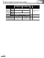
SERIAL COMMUNICATION MODULE REPLACEMENT
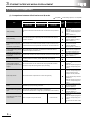
2.4 Switch Setting Comparison
(1) Comparison between A series and Q series
:Compatible,
:Partial change required, ×:Incompatible
Description
A series
Q series
AJ71UC24
QJ71C24N
QJ71C24N-R2
QJ71C24N-R4
Switch name
Compatibility
Precautions for
replacement
Reference
section
Each of the interface modes’ setting is
determined by the data communication
function to be used.
RS-232
0
Mode switch
Station number switch
RS-422/485
Use not allowed
1
to
4
Dedicated
protocol
(format1 to 4)
5
to
8
Non-procedural
mode
or
bidirectional
mode
Non-procedural
mode
or
bidirectional
mode
Dedicated
protocol
(format1 to 4)
9
Non-procedural mode
A
to
D
Dedicated protocol (format1 to 4)
E
Use not allowed
F
Self-loopback test
Set the switch settings
in the GX Developer
PLC parameter
settings.
Refer to Section 2.4
-
(3)*1.
The station number of the module for
when date communications is performed
using dedicated protocol is set.
-
Section 2.7
SW11
Main channel
setting
The target interface of transmission
processing and reception processing is
set.
-
SW12
Data bit
setting
The data bit length of the data to be
transmitted/received is set.
-
SW13
Transmission
to
speed setting
SW15
The transmission speed for when data is
to be transmitted/received is set.
-
Parity bit
SW16 enable/disable
setting
The parity bit ON/OFF of the data to be
sent/received is set.
-
The type of parity bit to add to the data to
be transmitted/received is set.
-
The stop bit length of the data to be
transmitted/received is set.
-
Sum check
SW21 enable/disable
setting
The sum check code presence in
dedicated protocol data communications
is set.
-
Write during
SW22 RUN enable/
disable setting
Write during RUN enable/disable in
dedicated protocol data communications
is set.
-
computer link/
SW23 multidrop link
selection
The function of computer link module to
be used is set.
-
-
master/local
station setting
The station type for use of multidrop link
function is set.
-
-
Even/odd parity
Transmission SW17
setting
specification
Stop
switch
SW18
bit setting
SW24
-
There is no distinction
with the main channel
on the Q series.
Set the switch settings
in the GX Developer
PLC parameter
settings.
Refer to Section 2.4
(3)*1.
There is no multidrop
link function provided
for the Q series.
2 - 15
2
SERIAL COMMUNICATION MODULE REPLACEMENT
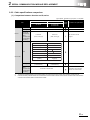
(2) Comparison between AnS series and Q series
(a) A1SJ71UC24-R2
:Compatible,
:Partial change required, ×:Incompatible
Description
Switch name
AnS series
Q series
A1SJ71UC24-R2
QJ71C24N
QJ71C24N-R2
Compatibility
Precautions for
replacement
Reference
section
Each of the interface modes’ setting is
determined by the data communication
function to be used.
RS-232 (CH1)
Mode switch
1
to
4
Dedicated protocol (format1 to 4)
5
Non-procedural mode
or
bidirectional mode
6
to
E
Use not allowed
F
Self-loopback test
A1ADP-SP
setting
-
-
-
Write during
SW04 RUN enable/
disable setting
Write during RUN enable/disable in
dedicated protocol data communications
is set.
-
SW05
Transmission
to
speed setting
SW07
The transmission speed for when data is
to be transmitted/received is set.
-
The data bit length of the data to be
transmitted/received is set.
-
The parity bit ON/OFF of the data to be
sent/received is set.
-
Transmission SW08 Data bit setting
specification
Parity bit
switch
SW09 enable/disable
setting
SW10
Even/odd parity The type of parity bit to add to the data to
setting
be transmitted/received is set.
SW11
Stop bit setting
Sum check
SW12 enable/disable
setting
*1
Use not allowed
The station number of the module for
when date communications is performed
using dedicated protocol is set.
Station number switch
SW03
0
-
Set the switch settings
in the GX Developer
PLC parameter
Section 2.7
settings.
Refer to Section 2.4
(3)*1.
-
The stop bit length of the data to be
transmitted/received is set.
-
The sum check code presence in
dedicated protocol data communications
is set.
-
Using the A1SJ71UC24-R2 with the A1ADP-SP
When the A1SJ71UC24-R2 with the software version X or later is used, the A1ADP-SP setting can be used.
This setting is used to create a sequence program in the nonprocedural mode by using dedicated instructions for the
computer link function in the AnACPU.
When using dedicated instructions for the computer link function, switch the A1ADP-SP setting to ON. When not using
them, switch the setting to OFF.
When the A1SJ71UC24-R2 with the software version W or earlier is used, the dedicated instructions for the computer link
function cannot be used.
Create a sequence program using the FROM/TO instructions.
2 - 16
2
SERIAL COMMUNICATION MODULE REPLACEMENT
(b) A1SJ71UC24-R4
:Compatible,
:Partial change required, ×:Incompatible
Description
Switch name
AnS series
Q series
A1SJ71UC24-R4
QJ71C24N
QJ71C24N-R4
Compatibility
Precautions for
replacement
Reference
section
Each of the interface modes’ setting is
determined by the data communication
function to be used.
RS-422/485 (CH2)
Mode switch
0
to
3
Use not allowed
4
Non-procedural mode
or
bidirectional mode
5
to
8
Dedicated protocol (format1 to 4)
9
to
E
Use not allowed
F
Self-loopback test
(3)*1.
The station number of the module for
when date communications is performed
using dedicated protocol is set.
-
master/local
station setting
The station type for use of multidrop link
function is set.
-
computer link/
SW02 multidrop link
selection
The function of computer link module to
be used is set.
-
-
-
-
Station number switch
SW01
SW03
A1ADP-SP
setting
Write during
SW04 RUN enable/
disable setting
SW05
Transmission
Transmission to
speed setting
specification SW07
switch
SW08 Data bit setting
Parity bit
SW09 enable/disable
setting
Write during RUN enable/disable in
dedicated protocol data communications
is set.
-
The transmission speed for when data is
to be transmitted/received is set.
-
The data bit length of the data to be
transmitted/received is set.
-
The parity bit ON/OFF of the data to be
sent/received is set.
-
Even/odd parity The type of parity bit to add to the data to
SW10
setting
be transmitted/received is set.
SW11
Stop
bit setting
Sum check
SW12 enable/disable
setting
*1
Set the switch settings
in the GX Developer
PLC parameter
settings.
Refer to Section 2.4
-
-
There is no multidrop
link function provided
for the Q series.
Section 2.7
Set the switch settings
in the GX Developer
PLC parameter
settings.
Refer to Section 2.4
(3)*1.
-
The stop bit length of the data to be
transmitted/received is set.
-
The sum check code presence in
dedicated protocol data communications
is set.
-
When the A1SJ71UC24-R4 is mounted to the A1ADP-SP
When the A1SJ71UC24-R4 with the software version X or later, the A1ADP-SP setting can be used.
This setting is used to create a sequence program in the non-procedural mode by using the dedicated instructions for the
computer link function in the AnACPU.
When using the dedicated instructions for the computer link module, switch the A1ADP-SP setting to ON. When not using
them, switch the setting to OFF.
When the A1SJ71UC24-R4 with the software version W or earlier is used, the dedicated instructions for the computer link
function cannot be used.
Create a sequence program using the FROM/TO instructions.
2 - 17
2
SERIAL COMMUNICATION MODULE REPLACEMENT
(3) Comparison between QnA/QnAS series and Q series
:Compatible,
:Partial change required, ×:Incompatible
Description
QnA series
Switch name
AJ71QC24N
AJ71QC24N-R2
AJ71QC24N-R4
Q series
A1SJ71QC24N1
A1SJ71QC24N1-R2
QJ71C24N
QJ71C24N-R2
QJ71C24N-R4
Mode switch
Each of the interface modes’ setting is
determined by the data communication
function to be used.
0: (For independent operation/linked
operation)
1: Dedicated protocol (format 1)
2: Dedicated protocol (format 2)
3: Dedicated protocol (format 3)
4: Dedicated protocol (format 4)
5: Dedicated protocol (format 5)
6: Nonprocedural protocol
7: Bidirectional protocol
8 to D: Setting unavailable
E: ROM/RAM/switch test
F: Self-loopback test
-
Station number switch
The station number of the module for
when data communications is performed
using dedicated protocol is set.
-
Operation (independent operation/linked
operation) of the two interfaces is set.
-
SW02 Data bit setting
The data bit length of the data to be
transmitted/received is set.
-
Parity bit
SW03 enable/disable
setting
The parity bit ON/OFF of the data to be
sent/received is set.
-
SW01
SW04
Operation
setting
Even/odd parity The type of parity bit to add to the data to
setting
be transmitted/received is set.
The sum check code ON/OFF in
dedicated protocol/bidirectional protocol
data communications is set.
-
Write during RUN enable/disable in
dedicated protocol data communications
is set.
-
Setting change
SW08 enable/disable
setting
Mode switching and E2PROM write
enabled/disabled are set.
-
SW09
Transmission
to
speed setting
SW12
The transmission speed for when data is
to be transmitted/received is set.
-
SW13
to
SW15
(All switches are set to OFF.)
-
-
Precautions for
replacement
Reference
section
Set the switch settings
in the GX Developer
PLC parameter
-
Sum check
Transmission
SW06 enable/disable
specification
setting
switch
Write during
SW07 RUN enable/
disable setting
Compatibility
settings.*1
The stop bit length of the data to be
transmitted/received is set.
SW05 Stop bit setting
2 - 18
QnAS series
-
Section 2.7
2
SERIAL COMMUNICATION MODULE REPLACEMENT
*1
The Q series serial communication module switch setting is set in the GX Developer PLC parameter settings.
2 - 19
2
SERIAL COMMUNICATION MODULE REPLACEMENT
2.5 Program Comparison
2.5.1 I/O signal
(1) Comparison between A/AnS series and Q series
There is no compatibility in the I/O signal assignments between the A/AnS series and the Q series.
Make a new sequence program.
:Compatible,
:Partial change required, ×:Incompatible
Signal name
Input signal
A series
AnS series
AJ71UC24
A1SJ71UC24-R2
A1SJ71UC24-R4
Compatibility
Precautions for replacement
Xn0
Transmission complete
On the Q series, Xn0, Xn1, Xn7, and Xn8 are used as the transmission
complete signals.
Xn1
Receive data read request
On the Q series, Xn3, Xn4, XnA, and XnB are used as the read request,
receive data, and read request signals.
Xn2
Global signal
Xn3
Xn4
Xn5
Xn6
Xn7
On the Q series, X(n+1)A and X(n+1)B are used as global signals.
On-demand in execution
Transmission complete of on-demand data is confirmed by the complete
device of the ONDEMAND instruction.
Computer link module
Transmission sequence status
The status is confirmed by the transmission sequence state storage area
(addresses: 597(256H), 613(265H)) in buffer memory.
Computer link module ready
Xn8
Use prohibited
Xn9
Mode switching complete
XnA
On the Q series, X(n+1)E is used as the ready signal.
On the Q series, Xn8 is used as the abnormal completion of transmission
signal.
On the Q series, Xn6 is used as the mode switching complete signal.
On the Q series, XnA and XnB are used as signals for various applications.
(Refer to Section 2.5.1 (2).)
Use prohibited
XnB
XnC
Use prohibited
XnD
Watchdog timer
On the Q series, X(n+1)F is used as the watchdog timer signal.
XnE
to
X(n+1)F
Use prohibited
On the Q series, XnE to X(n+1)F are used as signals for various applications.
(Refer to Section 2.5.1 (2).)
Signal name
Output signal
A series
AnS series
AJ71UC24
A1SJ71UC24-R2
A1SJ71UC24-R4
Yn0
to
YnF
Use prohibited
Y(n+1)0
Send request
Y(n+1)1
Receive data read complete
Y(n+1)2
to
Y(n+1)8
Use prohibited
Y(n+1)9
Mode switching request
Y(n+1)A
Y(n+1)B
Y(n+1)C
Y(n+1)F
2 - 20
Precautions for replacement
On the Q series, Yn0 to YnF are used as signals for various applications.
(Refer to Section 2.5.1 (2).)
On the Q series, Yn0 and Yn7 are used as the send request signals.
On the Q series, Yn1 and Yn8 are used as the receive data read complete
signals.
On the Q series, Y(n+1)2 to Y(n+1)8 are used as signals for various
applications. (Refer to Section 2.5.1 (2).)
On the Q series, Yn2 and Yn9 are used as the mode switching request signals.
Use prohibited
Use prohibited
Y(n+1)D
Y(n+1)E
Compatibility
Use prohibited
On the Q series, Y(n+1)C is used as the system setting default request signal.
2
SERIAL COMMUNICATION MODULE REPLACEMENT
(2) Comparison between QnA/QnAS series and Q series
:Compatible,
:Partial change required, ×:Incompatible
Signal name
QnA series
Input signal
AJ71QC24N
AJ71QC24N-R2
AJ71QC24N-R4
QnAS series
Q series
A1SJ71QC24N1
A1SJ71QC24N1-R2
QJ71C24N
QJ71C24N-R2
QJ71C24N-R4
Xn0
Normal completion of transmission
Normal completion of
transmission
Xn1
Abnormal completion of transmission
Abnormal completion of
transmission
CH1
CH1
Xn2
Transmission processing in progress
Transmission processing in
progress
Xn3
Receive data read request
Receive data read request
Xn4
Receive error detection
Receive error detection
Xn5
(System use)
(System use)
Xn6
CH1 mode switching
CH1 mode switching
Xn7
Normal completion of transmission
Normal completion of
transmission
Xn8
Abnormal completion of transmission
Abnormal completion of
transmission
CH2
CH2
Xn9
Transmission processing in progress
Transmission processing in
progress
XnA
Receive data read request
Receive data read request
XnB
Receive error detection
Receive error detection
XnC
(System use)
(System use)
XnD
CH2 mode switching
CH2 mode switching
XnE
CH1 ERR.LED ON
CH1 error.
XnF
CH2 ERR.LED ON
CH2 error.
X(n+1)0
Modem initialization completion
Modem initialization completion
X(n+1)1
Dialing
Dialing
X(n+1)2
Connecting
Line connection
X(n+1)3
Abnormal completion of initialization/connection
Initialization, line connection failure
X(n+1)4
Modem disconnection completion
Line disconnection completion
X(n+1)5
Normal completion of notification
Normal completion of notification
X(n+1)6
Abnormal completion of notification
Abnormal completion of notification
X(n+1)7
2
E PROM read complete
2
Compatibility
Precautions for
replacement
Flash ROM read complete
X(n+1)8
E PROM write complete
Flash ROM write complete
X(n+1)9
E2PROM system setting write complete
Flash ROM system setting completion
X(n+1)A
CH1 global signal
CH1 global signal
X(n+1)B
CH2 global signal
CH2 global signal
X(n+1)C
System setting default completion
System setting default completion
X(n+1)D
(System use)
(System use)
X(n+1)E
QC24N ready signal (accessible)
C24 ready signal
X(n+1)F
Watchdog timer
Watchdog timer
2 - 21
2
SERIAL COMMUNICATION MODULE REPLACEMENT
:Compatible,
:Partial change required, ×:Incompatible
Signal name
QnA series
Output signal
AJ71QC24N
AJ71QC24N-R2
AJ71QC24N-R4
Yn0
Yn1
QnAS series
Q series
A1SJ71QC24N1
A1SJ71QC24N1-R2
QJ71C24N
QJ71C24N-R2
QJ71C24N-R4
Send request
CH1
Yn2
Receive data read complete
Send request
CH1
Mode switching request
Receive data read complete
Mode switching request
Yn3
Yn4
Use prohibited
Yn5
Use prohibited
Yn6
Yn7
Yn8
Yn9
Send request
CH2
Receive data read complete
Mode switching request
Send request
CH2
Receive data read complete
Mode switching request
YnA
YnB
Use prohibited
Use prohibited
YnE
CH1 ERR.LED OFF request
CH1 side error information initialization
request
YnF
CH2 ERR.LED OFF request
CH2 side error information initialization
request
Y(n+1)0
Modem initialization request
Modem initialization request
Y(n+1)1
Connection request
Line connection request
Y(n+1)2
Modem disconnection request
Line disconnection request
YnC
YnD
Y(n+1)3
Use prohibited
Use prohibited
Y(n+1)4
Notification issue request
Notification issue request
Use prohibited
Use prohibited
Y(n+1)5
Y(n+1)6
Y(n+1)7
E2PROM
read request
Flash ROM read request
Y(n+1)8
E2PROM write request
Flash ROM write request
Y(n+1)9
E2PROM system setting write request
Flash ROM system setting request
Use prohibited
Use prohibited
System setting default request
System setting default request
Use prohibited
Use prohibited
Y(n+1)A
Y(n+1)B
Y(n+1)C
Y(n+1)D
Y(n+1)E
Y(n+1)F
2 - 22
Compatibility
Precautions for
replacement
2
SERIAL COMMUNICATION MODULE REPLACEMENT
2.5.2 Buffer memory
(1) Comparison between A/AnS series and Q series
There is no compatibility in the buffer memory assignments between the A/AnS series and the Q series.
Make a new sequence program.
The table below shows the main assignment areas for the initial settings and for transmission/reception.
:Compatible,
Buffer memory address
Buffer memory name
A series
AnS series
AJ71UC24
A1SJ71UC24-R2
A1SJ71UC24-R4
HEX
DEC
0H
0
Non-procedural send data count storage
area
1H to 7FH
1 to 127
Send data storage area
80H
128
Non-procedural receive data count
storage area
81H to FFH
129 to 255
Receive data storage area
100H
256
Non-procedural receive end code
specification
to
103H
*1
On the Q series, the area from address 401H, 801H (1025, 2049)
is used as the send data specification area.
On the Q series, the area of address 600H, A00H (1536, 2560) is
used as the receive data count specification area.
On the Q series, the area from address 601H, A01H (1537, 2561)
is used as the receive data storage area.
On the Q series, the area of address A5H, 145H (165, 325) is used
as the receive end code specification area.
On the Q series, the area from address 101H (257) onward is
On the Q series, the area of 96H, 136H (150, 310) is used as the
On the Q series, the area of address A2H, 142H (162, 322) is used
261
Non-procedural send buffer memory
length specification area
106H
262
Non-procedural receive buffer memory
head address specification area
263
Non-procedural receive buffer memory
length specification area
108H
264
Non-procedural receive end data count
specification area
109H
265
On-demand buffer memory head
address specification area
DFFH
used as the send data count specification area.
259
105H
10CH to
On the Q series, the area of address 400H, 800H (1024, 2048) is
Non-procedural word/byte specification
area
Non-procedural send buffer memory
head address specification area
10BH
Precautions for replacement
to
260
10AH
Compatibility
to
104H
107H
:Partial change required, ×:Incompatible
266
On-demand length specification area
267
RS-232 CD terminal check setting area
268 to 3583
-
used for various applications.
word/byte unit specification area.*1
as the send buffer memory head address specification area.*1
On the Q series, the area of address A3H, 143H (163, 323) is used
as the send buffer memory length specification area.*1
On the Q series, the area of address A6H, 146H (166, 326) is used
as the receive buffer memory head address specification area.*1
On the Q series, the area of address A7H, 147H (167, 327) is used
as the receive buffer memory buffer memory length specification
area.*1
On the Q series, the area of address A4H, 144H (164, 324) is used
as the receive end data count specification area.*1
On the Q series, the area of address A0H, 140H (160, 320) is used
as the on-demand buffer memory head address specification
area.*1
On the Q series, the area of address A1H, 141H (161, 321) is used
as the on-demand data length specification area.*1
On the Q series, the area of 97H, 137H (151, 311) is used as the
CD terminal check specification area.*1
On the Q series, the area from address 10CH (152) onward is
used for various applications.
Make the initial setting on the utility package (GX Configurator-SC).
2 - 23
2
SERIAL COMMUNICATION MODULE REPLACEMENT
(2) Comparison between QnA/QnAS series and Q series
The table below shows the main assignment areas for the initial settings and for transmission/reception.
:Compatible,
Buffer memory address
:Partial change required, ×:Incompatible
Buffer memory name
QnA series
AJ71QC24N
AJ71QC24N-R2
AJ71QC24N-R4
QnAS series
Q series
A1SJ71QC24N1
A1SJ71QC24N1-R2
QJ71C24N
QJ71C24N-R2
QJ71C24N-R4
HEX
DEC
0H
0
to
to
to
to
2EH to 38H
46 to 56
Modem Function area
(For initial setting)
Modem function specification-1 area
(For initial setting)
39H to 8FH
57 to 143
System area (use prohibited)
System area (use prohibited)
90H, 130H
144, 304
91H, 131H
145, 305
Mode switching area
Mode switching specification area
92H, 132H
146, 306
System area (use prohibited)
RS•DTR signal status spefication area
93H, 133H
147, 307
DTR/DSR, DC control
specification area
DTR/DSR, DC control
specification area
94H, 134H
148, 308
DC1/DC3 code specification area
DC1/DC3 code specification area
95H, 135H
149, 309
DC2/DC4 code specification area
DC2/DC4 code specification area
96H, 136H
150, 310
Word/byte specification area
Word/byte specification area
97H, 137H
151, 311
RS-232
CD terminal check setting area
RS-232
CD terminal check setting area
to
to
to
to
A0H, 140H
160, 320
On-demand buffer memory head address
specification area
On-demand buffer memory head address
specification area
A1H, 141H
161, 321
On-demand data length specification area
On-demand data length specification area
A2H, 142H
162, 322
Send buffer memory
head address specification area
Send buffer memory
head address specification area
A3H, 143H
163, 323
Send buffer memory length specification area
Send buffer memory length specification
area
A4H, 144H
164, 324
Receive end data count specification area
Receive end data count specification area
A5H, 145H
165, 325
Receive end code specification area
Receive end code specification area
A6H, 146H
166, 326
receive buffer memory head address specification
area
receive buffer memory head address
specification area
A7H, 147H
167, 327
receive buffer memory length specification area
receive buffer memory length
specification area
to
to
to
to
System setting area
200H to
220H
221H to
23DH
23EH
23FH to
24EH
CH1 LED OFF, communication error clear request
area
LED, communication error clear area
System information area
System information area
545 to 573
Modem function area
Modem function area
574
System information area
-
Use the default
value.
System area (use prohibited)
System area (use prohibited)
24FH
591
to
to
to
to
3FFH
1023
System area (use prohibited)
System area (use prohibited)
400H
1024
401H to
5FFH
station No. setting check area
CH1 transfer buffer memory
CH1 transfer buffer memory
Send data count specification area
Send data count specification area
1025 to
1535
Send data specification area
Send data specification area
600H
1536
Receive data count
specification area
Receive data count
specification area
601H to
1537 to
2047
Receive data storage area
Receive data storage area
7FFH
Precautions for
replacement
CH1 LED OFF, communication error
clear request area
512 to 544
575 to 590
Compatibility
-
(Continued on next page)
2 - 24
2
SERIAL COMMUNICATION MODULE REPLACEMENT
:Compatible,
Buffer memory address
QnA series
HEX
DEC
800H
2048
801H to
9FFH
:Partial change required, ×:Incompatible
Buffer memory name
AJ71QC24N
AJ71QC24N-R2
AJ71QC24N-R4
QnAS series
Q series
A1SJ71QC24N1
A1SJ71QC24N1-R2
QJ71C24N
QJ71C24N-R2
QJ71C24N-R4
CH2 transfer buffer memory
CH2 transfer buffer memory
Send data count specification area
Send data count specification area
2049 to
2559
Send data specification area
Send data specification area
A00H
2560
Receive data count specification area
Receive data count specification
area
A01H to
2561 to
3071
Receive data storage area
Receive data storage area
BFFH
C00H to
3072 to
6911
User free area
User free area
6912 to
8182
User frame
registration area
User registration area
1FFFH
8183 to
8191
System area
(use prohibited)
System area
(use prohibited)
2000H
8192
2001H to
8193 to
32767
1AFFH
1B00H to
1FF6H
1FF7H to
7FFFH
Flash ROM write enable/disable
specification area
(Area for new function)
Compatibility
Precautions for
replacement
-
An additional
sequence program is
required depending
on the functions to be
used.
2 - 25
2
SERIAL COMMUNICATION MODULE REPLACEMENT
2.6 Reuse of Existing Programs
2.6.1 Reuse of A/AnS series programs
Data communications between programmable controller CPU and external device, and between
programmable controller CPUs that was performed by the A/AnS series computer link module can also
be performed using Q series serial communication modules.
The following shows a description of how to reuse programs for A/AnS series computer link module for
use on a Q series serial communication module at replacement of modules.
Item
Initial setting
Relevant device
Programmable
controller CPU
[Access to another station]
When accessing other station's programmable controller CPU
via MELSECNET/H, set "Valid module during other station
access" in the GX Developer network parameters.
[Data transmission by the on-demand function]
Change to a sequence program that uses the dedicated
instruction (ONDEMAND).
[Accessing the programmable controller CPU]
The available commands, accessible device range, and access
Communication
target device
Bidirectional
communication
(Bidirectional protocol
communication)
Remarks
Programmable
controller CPU
Communication using
dedicated protocol
(MC protocol
communication)
Non-procedural
communication
(Non-procedural protocol
communication)
Description
[Initial Setting on the Utility Package]
Make the initial setting on the utility package (GX ConfiguratorSC).
Refer to the Q Corresponding
[Deleting the initial setting program]
Serial Communication Module
Delete the initial setting program.
User's Manual (Basic).
[Setting the sum check code of the bidirectional protocol]
When appending messages with the sum check code in
bidirectional protocol communications, set the switches in the
GX Developer PLC parameters.
to another station are restricted.*1 *2
[Access to another station]
Another station cannot be accessed via the data link system
(MELSECNET(II), MELSECNET/B).
• Refer to the GX Developer
Operating Manual.
• Refer to the Q Corresponding
Serial Communication Module
User's Manual (Basic).
• Refer to the MELSEC
communication protocol
reference manual.
Programmable
controller CPU
[Transmission/reception of data]
Change to a sequence program that uses the dedicated
instructions (INPUT, OUTPUT).
Communication
target device
[Transmission of data]
When receiving by the receive end code on the programmable
controller CPU side, transmit the data (default, CR+LF (codes: Refer to the Q Corresponding
Serial Communication Module
0DH, 0AH)) of the end code at the end of the data to be
User's Manual (Basic).
transmitted to the programmable controller CPU.*3
Programmable
controller CPU
[Transmission/reception of data]
Change to a sequence program that uses the dedicated
instructions (BIDIN, BIDOUT).
[Printing messages on a printer]
Transmission using printer
function
Programmable
controller CPU
Programmable
controller CPU
Others
2 - 26
Programmable
controller CPU
and
Communication
target device
When messages*4 were being printed on a printer, create a
transmission program using user frames of the Q series serial
communication module.*5
Delete programs that use the regular printer function.
[Assignment of I/O signals]
There is no compatibility in the I/O signal (X/Y) assignments
between the A/AnS series and the Q series.
Check the I/O signals (X/Y) in use, and correct the program.
Refer to the Q Corresponding
Serial Communication Module
User's Manual (Application).
Refer to the Q Corresponding
Serial Communication Module
[Assignment of buffer memory]
User's Manual (Basic).
There is no compatibility in the buffer memory assignments
between the A/AnS series and the Q series.
Check the target buffer memories and addresses of the data to
read/write, and correct the program.
2
SERIAL COMMUNICATION MODULE REPLACEMENT
*1
Only accessing of device memory on the programmable controller CPU is available.
Accessible device range is the same as that on the A/AnS series programmable controller CPU.
The following devices cannot be accessed from external devices:
• Devices newly added on by QCPU
• Latch relays (L) and step relays (S)
*In the case of QCPU, latch relays (L) and step relays (S) are different devices from internal relays (M). Internal relays,
however, are accessed whichever of these relays is specified.
• File registers (R)
To use a function other than accessing of device memories, access using the new commands for the Q series serial
communication module.
(Create a new program.)
*2
The following devices in special relays (M9000 onwards) and special registers (D9000 onwards) are accessed:
• SD1000 to SD1255 are accessed by specifying D9000 to D9255.
• SM1000 to SM1255 are accessed by specifying M9000 to M9255.
*3
In the same way as when an A/AnS series computer link module is used, any receive end code can be registered to a Q
*4
Messages that are handled by an A/AnS series computer link module become user frames on a Q series serial
*5
Messages (user frames) can be registered on the utility package (GX Configurator-SC).
series serial communication module, and data can be transmitted to external devices as a result of this.
communication module.
Messages are transmitted by the dedicated instruction (PRR).
2 - 27
2
SERIAL COMMUNICATION MODULE REPLACEMENT
2.6.2 Reuse of QnA/QnAS series programs
Data communications between programmable controller CPU and external device, and between
programmable controller CPUs that was performed by the QnA/QnAS series serial communication
module can also be performed using Q series serial communication modules.
The following shows a description of how reuse programs for a QnA/QnAS series serial communication
module for use on a Q series serial communication module at replacement of module.
Item
Communication using link
instruction
Others
2 - 28
Relevant device
Description
Remarks
Programmable
controller CPU
[Data communications by link instructions]
Link instructions are not provided with a function for performing
data communications with another stations programmable
controller CPU on a multidrop connection.
The communications method must be changed (e.g.
communications via MELSECNET/H).
Delete the data communications program using the link
instruction.
Communication
target device
[Data communications on the RS-422/485 interface]
The precautions during data communications are the same as
when a QnA/QnAS series serial communication module is
Refer to the Q Corresponding
used.
Serial Communication Module
First check operation of the RS-422/485 interface on the
User's Manual (Basic).
programmable controller CPU side, and then insert a wait time,
etc. to adjust the data transmission/reception timing.
2
SERIAL COMMUNICATION MODULE REPLACEMENT
2.7 Other Precaution
The following shows the precautions relating to Q series serial communication modules when A/AnS/
QnA/QnAS series programmable controllers are replaced with Q series programmable controllers.
(1) About processing time
The processing time for data communications differs between the A/AnS/QnAQnAS and Q series
modules.
For this reason, some data communications timing may be also different. If necessary, adjust the timing
by inserting a wait time, for example.
For actual details on processing times, refer to the manual for the respective module.
(2) About switch settings
When using a Q series serial communication module, be sure to set the operation mode, station number
and transmission specifications in the following parameter setting screen on GX Developer.
• "Switch setting for intelligent function module" screen
The Q series serial communication module does not have setting switches for setting the mode setting,
station number setting and transmission specifications setting.
(3) About the RS-422 interface
Q series communication modules do not have the connector specifications RS-422 interface (CH1) that
is available on the QnA series communication module AJ71QC24N-R4.
Use the RS-232 interface or terminal block specifications RS-422/485 interface to connect to external
devices.
(4) About data communications on the RS-422/485 interface
The precautions during data communications on the RS-422/485 interface are the same as when a
QnA/QnAS series serial communication module is used. When external devices may receive the wrong
data, attach a pullup/pulldown transistor on the external device side.
2 - 29
2
SERIAL COMMUNICATION MODULE REPLACEMENT
2.8 Program Examples
The following shows an example of how to change the nonprocedural communications program on the
A/AnS series computer link module for use on a Q series serial communication module when replacing
an A/AnS series programmable controller with a Q series programmable controller.
When applying the program examples introduced in this section to an actual program, sufficiently study
if there will be any problem in control on the target system.
(1) Program example of A/AnS series computer link module
Programmable
controller CPU
Send
enable
flag
M10
Data writing
Address
0H
Data sending
TOP
SET
X0
AJ71UC24
Buffer memory
Personal
computer
Send request
RST
Send completion
Read request
X1
FROMP
Buffer memory
Data reading
Address
80H
Y11
Read completion
(When using FROM/TO instruction)
2 - 30
Data receiving
2
SERIAL COMMUNICATION MODULE REPLACEMENT
(a) When using application instruction (FROM/TO)
Transmission processing
Writes No. of send data.
Send
enable
flag
Module Transmis- Send
ready sion com- request
signal plete
Writes send data.
Send
data
Send
request
Send
request
Transmission complete
Transmission normal
complete flag
Send completion
check flag
Receive
data read
Turns OFF the send request
signal upon transmission
completion.
(Flag control at transmission
completion)
Transmission normal
complete flag
No.of receive
data
No.of receive
data
Reception processing
Reads No. of receive data.
Transfers the No. of receive
data to the index register.
Reads received amount of data.
Receive
data
Receive data
read complete
Reception normal
complete flag
Receive completion
check flag
Performs send request.
Turns ON the read complete
signal of the receive data.
(Flag control at reception
completion)
Reception normal
complete flag
2 - 31
2
SERIAL COMMUNICATION MODULE REPLACEMENT
(b) When using dedicated instruction (PRN/INPUT)
Transmission processing
Send
enable
flag
Module
ready
signal
Transmis- Send
sion com- request
plete
Specifies the module's head I/O
signal.
Specifies No. of send data.
Send
data
Transmission
complete
Specifies send data.
Specifies a device by which
execution completion can be
checked.
(Instruction execution)
Transmission
complete
Send completion
check flag
Transmission normal
complete flag
(Flag control at transmission
completion)
Transmission normal
complete flag
Allowable No. of
receive data
Reception processing
Specifies allowable No. of receive
data.
Receive
data read
Specifies the module's head I/O
signal.
Allowable No. of
receive data
Receive
data
Reception
complete
Specifies allowable No. of receive
data.
Specifies a head device from
which receive data are stored.
Specifies a device by which
execution completion can be
checked.
(Instruction execution)
Receive
complete
Reception normal
complete flag
Receive completion
check flag
Reception normal
complete flag
2 - 32
(Flag control at reception
completion)
2
SERIAL COMMUNICATION MODULE REPLACEMENT
(2) Example of program for Q series serial communication module
Programmable
controller CPU
Send
enable
flag
QJ71C24N
Buffer memory
Data writing
M10
OUTPUT
Address
400H
Data sending
Personal
computer
Send request
Send completion
M0
Read request
Buffer memory
X3
Address
X4
Data reading
600H
INPUT
M20
Read completion
Data receiving
2 - 33
2
SERIAL COMMUNICATION MODULE REPLACEMENT
Interface
No.
Send
enable
flag
Transmission result
No. of send
data
Interface
No.
TransmisTransmission
sion comnormal/abnormal
plete
Transmission
normal/abnormal
Send
completion
check
flag
Send
data
Transmission complete
Transmission normal
complete flag
Transmission
failed flag
Transmission normal
complete flag
Transmission
failed flag
2 - 34
Transmission processing
Specifies channel No. for data
transmission.
Clears the device where the
transmission result is stored.
Specifies No. of send data.
(Instruction execution)
Data stored in the area starting
D11 from are sent.
(Flag control at reception
completion)
2
SERIAL COMMUNICATION MODULE REPLACEMENT
Interface
No.
CH1 read
request
Clears the device where the
reception result is stored.
Reception
result
CH1 reception
error
detection
Allowable No. of
receive data
Interface
No.
Reception Reception
complete normal/abnormal
Reception
normal/abnormal
Receive
completion
check
flag
Reception processing
Specifies channel No. for data
reception.
Reception
complete
Reception normal
complete flag
Specifies allowable No. of receive
data.
(Instruction execution)
Receive data are stored in the
area starting from D30.
(Flag control at reception
completion)
Reception
failed flag
Reception normal
complete flag
Reception
failed flag
2 - 35
3
ETHERNET INTERFACE MODULE REPLACEMENT
3
ETHERNET INTERFACE MODULE
REPLACEMENT
3
3.1 List of Ethernet Interface Modules to be Replaced
(1) Transition from A series to Q series
Network type
10BASE-T
10BASE5
10BASE2
A series
AJ71E71N3-T
AJ71E71N-B5
AJ71E71N-B2
Alternative model
QJ71E71-100
QJ71E71-B5
QJ71E71-B2
(2) Transition from AnS series to Q series
Network type
10BASE-T
10BASE5
10BASE2
AnS series
A1SJ71E71N3-T
A1SJ71E71N-B5
A1SJ71E71N-B2
Alternative model
QJ71E71-100
QJ71E71-B5
QJ71E71-B2
(3) Transition from QnA series to Q series
Network type
10BASE-T
10BASE5
10BASE2
QnA series
AJ71QE71N3-T
AJ71QE71N-B5
AJ71QE71N-B2
Alternative model
QJ71E71-100
QJ71E71-B5
QJ71E71-B2
(4) Transition from QnAS series to Q series
Network type
10BASE-T
10BASE5
10BASE2
3-1
QnAS series
A1SJ71QE71N3-T
A1SJ71QE71N-B5
A1SJ71QE71N-B2
Alternative model
QJ71E71-100
QJ71E71-B5
QJ71E71-B2
3
ETHERNET INTERFACE MODULE REPLACEMENT
3.2 Performance Specifications Comparison
3.2.1 Module performance comparison
(1) Comparison between A/AnS series and Q series
(a) 10BASE-T
: Compatible,
Specifications
Item
A series
AnS series
AJ71E71N3-T
Transmission speed
A1SJ71E71N3-T
10Mbps
Communication mode
Half-duplex
Full duplex/Half-duplex
Base band
Transmission Maximum segment
specifications length
100m*1
Maximum number of
nodes/connection
Up to two modules can be
connected in a cascade
connection when using at 100
Mbps.
Cascade connection: Up to 4
Number of allowable
simultaneously open
connections
8 connections
16 connections
Fixed buffer
1k word × 8
1k word × 16
Random access buffer
3k words × 2
6k words × 1
32 points/slot
(I/O assignment special 32 points)
32 points/slot
(I/O assignment intelli
32 points)
No. of occupied I/O points
*1
QJ71E71-100
CompatPrecautions for replacement
ibility
100Mbps/10Mbps
Transmission method
Transfer data
storage
memory
Q series
: Partial change required, ×: Incompatible
Change the sequence program
as buffer memory assignments
differ.
(Refer to Section 3.6.2.)
Length between hub and node
(b) 10BASE5
: Compatible,
Specifications
Item
A series
AnS series
Q series
AJ71E71N-B5
A1SJ71E71N-B5
QJ71E71-B5
Transmission speed
Half-duplex
Transmission method
Base band
Max. distance
Transmission between nodes
specifications Maximum segment
length
2500m
500m
Maximum number of
nodes/connection
100/segment
Minimum node
interval
Transfer data
storage
memory
2.5m
8 connections
16 connections
Fixed buffer
1k word × 8
1k word × 16
Random access buffer
3k words × 2
6k words × 1
32 points/slot
(I/O assignment special 32 points)
32 points/slot
(I/O assignment intelli
32 points)
No. of occupied I/O points
12V DC external power supply
capacity (Transceiver)
CompatPrecautions for replacement
ibility
10Mbps
Communication mode
Number of allowable
simultaneously open
connections
: Partial change required, ×: Incompatible
Change the sequence program
as buffer memory assignments
differ.
(Refer to Section 3.6.2.)
Use a transceiver and AUI cables that satisfy specifications.
3-2
3
ETHERNET INTERFACE MODULE REPLACEMENT
(c) 10BASE2
: Compatible,
Specifications
Item
A series
AnS series
Q series
AJ71E71N-B2
A1SJ71E71N-B2
QJ71E71-B2
Transmission speed
Half-duplex
Transmission method
Base band
Max. distance
Transmission between nodes
specifications Maximum segment
length
925m
185m
Maximum number of
nodes/connection
30/segment
Minimum node
interval
Transfer data
storage
memory
3-3
0.5m
8 connections
16 connections
Fixed buffer
1k word × 8
1k word × 16
Random access buffer
3k words × 2
6k words × 1
32 points/slot
(I/O assignment special 32 points)
32 points/slot
(I/O assignment intelli
32 points)
No. of occupied I/O points
CompatPrecautions for replacement
ibility
10Mbps
Communication mode
Number of allowable
simultaneously open
connections
: Partial change required, ×: Incompatible
Change the sequence program
as buffer memory assignments
differ.
(Refer to Section 3.6.2.)
3
ETHERNET INTERFACE MODULE REPLACEMENT
(2) Comparison between QnA/QnAS series and Q series
(a) 10BASE-T
: Compatible,
Specifications
Item
QnA series
QnAS series
AJ71QE71N3-T
Transmission speed
Communication mode
A1SJ71QE71N3-T
100Mbps/10Mbps
Half-duplex
Full duplex/Half-duplex
Transmission method
100m*1
8 connections
16 connections
1k word × 8
1k word × 16
Fixed buffer
Random access buffer
*1
Up to two modules can be
connected in a cascade
connection when using at 100
Mbps.
Cascade connection: Up to 4
Number of allowable
simultaneously open
connections
No. of occupied I/O points
CompatPrecautions for replacement
ibility
Base band
Maximum number of
nodes/connection
No. of E2PROM writes
QJ71E71-100
10Mbps
Transmission Maximum segment
specifications length
Transfer data
storage
memory
Q series
: Partial change required, ×: Incompatible
6k words × 1
Max. 100,000 times on same area in E2PROM
-
32 points/slot
(I/O assignment special 32 points)
32 points/slot
(I/O assignment intelli
32 points)
No E2PROM (Refer to Section
3.8.)
Length between hub and node
(b) 10BASE5
: Compatible,
Specifications
Item
QnA series
QnAS series
Q series
AJ71QE71N-B5
A1SJ71QE71N-B5
QJ71E71-B5
Transmission speed
Communication mode
Half-duplex
Transmission method
Base band
2500m
Transmission
specifications Maximum segment
length
500m
Maximum number of
nodes/connection
100/segment
Minimum node
interval
Number of allowable
simultaneously open
connections
Fixed buffer
Random access buffer
No. of E2PROM writes
No. of occupied I/O points
12V DC external power supply
capacity (Transceiver)
CompatPrecautions for replacement
ibility
10Mbps
Max. distance
between nodes
Transfer data
storage
memory
: Partial change required, ×: Incompatible
2.5m
8 connections
16 connections
1k word × 8
1k word × 16
6k words × 1
Max. 100,000 times on same area in E2PROM
-
32 points/slot
(I/O assignment special 32 points)
32 points/slot
(I/O assignment intelli
32 points)
No E2PROM (Refer to Section
3.8.)
Use a transceiver and AUI cables that satisfy specifications.
3-4
3
ETHERNET INTERFACE MODULE REPLACEMENT
(c) 10BASE2
: compatible,
Specifications
Item
QnA series
QnAS series
Q series
AJ71QE71N-B2
A1SJ71QE71N-B2
QJ71E71-B2
Transmission speed
Communication mode
Half-duplex
Transmission method
Base band
925m
185m
Maximum number of
nodes/connection
30/segment
Minimum node
interval
Number of allowable
simultaneously open
connections
Fixed buffer
Random access buffer
No. of E2PROM writes
No. of occupied I/O points
3-5
CompatPrecautions for replacement
ibility
10Mbps
Max. distance
Transmission between nodes
specifications Maximum segment
length
Transfer data
storage
memory
: partial change required, ×: Incompatible
0.5m
8 connections
16 connections
1k word × 8
1k word × 16
6k words × 1
Max. 100,000 times on same area in E2PROM
-
32 points/slot
(I/O assignment special 32 points)
32 points/slot
(I/O assignment intelli
32 points)
No E2PROM (Refer to Section
3.8.)
3
ETHERNET INTERFACE MODULE REPLACEMENT
3.2.2 Cable specifications comparison
The Q series can use connectable devices (e.g. hubs*1, cables, transceivers*2 *3) that are being used on
the A/AnS/QnAQnAS series.
For details on connectable devices, refer to the Q Corresponding Ethernet Interface Module User's
Manual (Basic).
*1
When connecting a hub that does not have the auto-negotiation function
On a connection with a hub that does not have the auto-negotiation function,
set the hub side to the half-duplex communication mode.
*2
About wiring of the external power supply terminal (for the transceiver) on the QJ71E71-B5
An FG terminal is not provided for the external power supply terminal on the QJ71E71-B5.
When handling the FG terminal on the external power supply (for the transceiver),
ground the FG signal on the external power supply side.
*3
The shape of the external power supply terminal (for the transceiver) differs between the QnA series QJ71QE71N-B5 and
the Q series QJ71E71-B5. When replacing the AJ71QE71N-B5 with the Q series QJ71E71-B5, refer to the following
manual for wiring.
Q Corresponding Ethernet Interface Module User's Manual (Basic)
3-6
3
ETHERNET INTERFACE MODULE REPLACEMENT
3.3 Function Comparison
(1) Comparison between A/AnS series and Q series
: Compatible,
: Partial change required, ×: Incompatible
Description
Item
A series
AnS series
Q series
AJ71E71N3-T
AJ71E71N-B5
AJ71E71N-B2
A1SJ71E71N3-T
A1SJ71E71N-B5
A1SJ71E71N-B2
QJ71E71-100
QJ71E71-B5
QJ71E71-B2
Compatibility
Precautions for replacement
Set in the GX Developer network
parameters.*1
(Delete the sequence program of
the section corresponding to the
function.)
(Refer to Section 3.9.)
Initial processing
The state in which data communications with an external device is possible is
set.
Open processing
The communications line for performing data communications with external
devices is connected.
Communications using fixed
buffer
(procedural, nonprocedural)
The fixed buffer on the Ethernet interface module is used to send/receive the
desired data between the programmable controller CPU and external devices.
Change to a sequence program
that uses the dedicated
instructions (BUFSND,
BUFRCV).(Refer to Section 3.9.)
Communications using random
access buffer
Data is read/written to the random access buffer of the Ethernet interface
module from multiple external devices.
Change the sequence program
as buffer memory assignments
differ. (Refer to Section 3.6.2.)
Read/write communications of
programmable controller CPU
internal data
Programmable controller CPU data is read/written to and from external devices.
Some of the commands and
device ranges are restricted.
(Refer to Section 3.7.)
Broadcast communication
Data is sent/received to all external devices on the same Ethernet network as
the Ethernet interface module by UDP/IP-based data communications.
(broadcast)
Change to a sequence program
that uses the dedicated
instructions (OPEN, CLOSE).*5
(Refer to Section 3.9.)
Set in the GX Developer network
Communications while the
Data communications can be continued when the programmable controller
programmable controller CPU is
CPU enters a stop state. (during passive open processing)
stopped
parameters.*2
(Delete the sequence program of
the section corresponding to the
function.)
Delete the sequence program of
the section corresponding to the
function, and set in the GX
Developer network parameters.
Router relay function
Data communications is performed via a router and a gateway.
*3
Set in the GX Developer network
parameters.*3
(Delete the sequence program of
the section corresponding to the
function.)
Existence check of external
device
Whether or not the external device is operating normally after the connection is
established (in open processing) is checked.
Communications using pairing
open
The connection is opened with connection for reception and
connection for transmission as a single pair. (for fixed buffer communications)
Unit of timer set values for data
communications
3-7
Set the unit (500 ms/2 s) of timer values
Fixed to 500 ms
Change to a sequence program
that uses the dedicated
instructions (OPEN).*5
Change to a sequence program
that uses the dedicated
instructions (OPEN).*4*5
Set in the GX Developer network
parameters.
(Delete the sequence program of
the section corresponding to the
function.)
The unit of timer set values is 500
ms.
3
ETHERNET INTERFACE MODULE REPLACEMENT
*1
Initial Processing
The Q series performs initial processing by setting the following items in the GX Developer network parameters.
• "Network parameters Setting the number of Ethernet/CC IE/MELSECNET cards"
• "Operational settings"
• "Initial settings"
There is no need for a sequence program for initial processing/end processing.
*2
Communications while the programmable controller CPU is stopped
By setting "Operational settings" - "Initial timing" to "Always wait for OPEN", the Q series can perform communications while
the programmable controller CPU is stopped.
For connections for which passive open and communications during a stop are set to enabled, it is not necessary to use a
sequence program for communications during a stop/open processing/close processing.
*3
Router relay function
The Q series sets the router relay function at "Network parameters" - "router relay parameter" on GX Developer.
There is no need for a sequence program for the router relay function.
3-8
3
ETHERNET INTERFACE MODULE REPLACEMENT
*4
Communications using pairing open
On the Q series, the pairing open setting of connection No.8 is not possible.
(Connection No.8 is pairing for reception, and connection No.1 is pairing for transmission.)
When the pairing open setting of connection No.8 has been made, change the sequence program.
On the Q series, the pairing open settings of connection No.1 to 7, and 9 to 15 are possible.
*5
Open processing
When "Operational settings" - "Initial timing" in GX Developer is set to "Always wait for OPEN", the sequence program using
dedicated instruction (OPEN/CLOSE) is not required.
3-9
3
ETHERNET INTERFACE MODULE REPLACEMENT
(2) Comparison between QnA/QnAS series and Q series
: Compatible,
: Partial change required, ×: Incompatible
Description
Item
Initial
processing
Sequence program
GX Developer
network parameters
QnA series
QnAS series
Q series
AJ71QE71N3-T
AJ71QE71N-B5
AJ71QE71N-B2
A1SJ71QE71N3-T
A1SJ71QE71N-B5
A1SJ71QE71N-B2
QJ71E71-100
QJ71E71-B5
QJ71E71-B2
Precautions for
replacement
Some communications
The state in which data communications with an external device is
possible is set.
Open processing
The communications line for performing data communications with
external devices is connected.
Communications using fixed buffer
(procedural, nonprocedural)
The fixed buffer on the Ethernet interface module is used to send/
receive the desired data between the programmable controller CPU
and external devices.
Communications using random
access buffer
Data is read/written to the random access buffer of the Ethernet
interface module from multiple external devices.
Read/write communications of
programmable controller CPU
internal data
Programmable controller CPU data is read/written to and from external
devices.
Communications using data link
instructions
Use data link instructions to read/write programmable controller CPU
data of other stations via Ethernet.
File transfer
(FTP server functions)
Use FTP commands to read/write individual files from external
devices.
Broadcast communication
Data is sent/received to all external devices on the same Ethernet
network as the Ethernet interface module by UDP/IP-based data
communications. (broadcast)
Communications while the
programmable controller CPU is
stopped
Compatibility
Data communications can be continued when the programmable
controller CPU enters a stop state. (during passive open processing)
are restricted.*1
Some of the commands
and device ranges are
restricted. (Refer to
Section 3.7.)
The default log-in name
and password have been
changed from
"AJ71QE71" to
"QJ71E71", so set the
log-in name again.
Delete the sequence
program of the section
corresponding to the
function, and set in the
GX Developer network
parameters.*2
MELSECNET/H,
MELSECNET/10 relay exchange
On a network system comprising a mixture of Ethernet and
MELSECNET/H or MELSECNET/10, or a network system that relays
through multiple Ethernets, data communications is performed via
these multiple networks.
Router relay function
Data communications is performed via a router and a gateway.
Existence check of external device
Whether or not the external device is operating normally after the
connection is established (in open processing) is checked.
The connection is opened with connection for reception and
Communications using pairing open connection for transmission as a single pair. (For fixed buffer
communications)
Parameter registration to E2PROM
*1
Saves parameters to E2PROM.
-
Some communications
are restricted.*3
Some communications
are restricted.*4
No E2PROM
(Refer to Section 3.8.)
Initial processing using a sequence program
• All of the items (e.g. data code setting) that were set on the QnA series exchange condition setting switch operate
in an OFF state.
To change the communication conditions, add the sequence program for re-initial processing.
• As the network number and station number cannot be set, the Ethernet interface module cannot be connected
with MELSOFT products (e.g. GX Developer).
To perform the above, perform initial processing by GX Developer network parameters.
3 - 10
3
ETHERNET INTERFACE MODULE REPLACEMENT
*2
Communications while the programmable controller CPU is stopped
By setting "Operational settings" - "Initial timing" to "Always wait for OPEN", the Q series can perform communications while
the programmable controller CPU is stopped.
For connections for which passive open and communications during a stop are set to enabled, it is not necessary to use a
sequence program for communications during a stop/open processing/close processing.
*3
MELSECNET/H, MELSECNET/10 relay exchange
On the Q series, Ethernet parameters (network number and station number) using the EPRSET instruction cannot be set.
When the EPRSET instruction is in use, delete the sequence program of the corresponding section, and set the Ethernet
parameters in the GX Developer network parameters.
*4
Communications using pairing open
On the Q series, the pairing open setting of connection No.8 is not possible.
(Connection No.8 is pairing for reception, and connection No.1 is pairing for transmission.)
When the pairing open setting of connection No.8 has been made, change the sequence program.
On the Q series, the pairing open settings of connection No.1 to 7, and 9 to 15 are possible.
3 - 11
3
ETHERNET INTERFACE MODULE REPLACEMENT
3.4 Switch Setting Comparison
(1) Comparison between A/AnS series and Q series
: Compatible,
: Partial change required, ×: Incompatible
Description
Switch name
Exchange
SW2
condition
setting
switch
SW7
SW8
*1
AnS series
Q series
A1SJ71E71N3-T
A1SJ71E71N-B5
A1SJ71E71N-B2
QJ71E71-100
QJ71E71-B5
QJ71E71-B2
Compatibility
Precautions for
replacement
Selects the operation mode.
0: Online
1: Offline
2: Test 1
(self-loopback test)
3: Test 2 (RAM test)
4: Test 3 (ROM test)
-
Set in GX Developer
network parameters.
(1) in *1)
Selection of line
processing at a
TCP timeout
error
Selects line processing when a TCP ULP
timeout error occurs.
OFF: Closes the line
ON: Does not close the line
-
Closes the line when a
TCP ULP timeout error
occurs.
Data code
setting
Selects the communications data code type.
OFF: Binary code
ON: ASCII code
-
Set in GX Developer
network parameters.
(2) in *1)
-
Set in GX Developer
network parameters.
(3) in *1)
-
A quick start is performed
(Initial processing starts
up with no delay time.)
Operation mode setting switch
SW1
A series
AJ71E71N3-T
AJ71E71N-B5
AJ71E71N-B2
CPU
Selects write during RUN enable/disable.
communications OFF: Write during RUN disabled
timing setting
ON: Write during RUN enabled
Initial timing
Selects the initial processing startup timing.
OFF: Quick start
ON: Normal start
GX Developer network parameters
2)
3)
1)
3 - 12
3
ETHERNET INTERFACE MODULE REPLACEMENT
(2) Comparison between QnA/QnAS series and Q series
: Compatible,
: Partial change required, ×: Incompatible
Description
Switch name
Operation mode setting switch
QnA series
QnAS series
Q series
AJ71QE71N3-T
AJ71QE71N-B5
AJ71QE71N-B2
A1SJ71QE71N3-T
A1SJ71QE71N-B5
A1SJ71QE71N-B2
QJ71E71-100
QJ71E71-B5
QJ71E71-B2
Selects the operation mode.
0: Online
1: Offline
2: Test 1 (self-loopback test)
3: Test 2 (RAM test)
4: Test 3 (ROM test)
Compatibility
Precautions for
replacement
-
Set in GX Developer
network parameters.
(1) in *1)
5: Test 4 (E2PROM test)
SW1
Selection of line
processing at a
TCP timeout
error
Selects line processing when a TCP ULP
timeout error occurs.
OFF: Closes the line
ON: Does not close the line
-
Closes the line when a
TCP ULP timeout error
occurs.
SW2
Data code
setting
Selects the communications data code type.
OFF: Binary code
ON: ASCII code
-
Set in GX Developer
network parameters.
(2) in *1)
Automatic
startup mode
setting
Selects the startup method when a module is
started.
OFF: Operation follows Y19
ON: Operation regardless of Y19
-
Exchange
condition
SW3
setting
switch
*1
SW7
CPU
Selects write during RUN enable/disable.
communications OFF: Write during RUN disabled
timing setting
ON: Write during RUN enabled
SW8
Initial timing
Selects the initial processing startup timing.
OFF: Quick start
ON: Normal start
Operation follows the
setting of Y19.*2
-
Set in GX Developer
network parameters.
(3) in *1)
-
A quick start is performed
(Initial processing starts
up with no delay time.)
GX Developer network parameters
2)
3)
1)
*2
When performing initial processing using GX Developer network parameters, initial processing is executed automatically.
(There is no need for a sequence program for initial processing/end processing.)
3 - 13
3
ETHERNET INTERFACE MODULE REPLACEMENT
3.5 Parameter Comparison
(1) Comparison between A/AnS series and Q series
On the A/AnS series, the parameters of the Ethernet interface module are set in the buffer memory.
On the Q series, however, the parameters are set using GX Developer network parameters.
Therefore, there is no compatibility between the parameters of the A/AnS series and the Q series.
When replacing the A/AnS series with the Q series, delete the parameter settings of the A/AnS series
and set new parameters on GX Developer.
(2) Comparison between QnA/QnAS series and Q series
: Compatible,
: Partial change required, ×: Incompatible
Description
Parameter name
QnA series
QnAS series
Q series
AJ71QE71N3-T
AJ71QE71N-B5
AJ71QE71N-B2
A1SJ71QE71N3-T
A1SJ71QE71N-B5
A1SJ71QE71N-B2
QJ71E71-100
QJ71E71-B5
QJ71E71-B2
Compatibility
Precautions for
replacement
Network type
Start I/O No.
Network No.
Group No.
Station No.
-
Mode
Network parameter
IP address setting
On the QnA series, the
mode was set on the
operation mode setting
switch.
Operational setting
-
Initial settings
-
Open settings
On the QnA series, the
setting was set in the
sequence program.
Station No. <-> IP information
FTP Parameters
Router relay parameter
Routing parameters
3 - 14
3
ETHERNET INTERFACE MODULE REPLACEMENT
3.6 Program Comparison
3.6.1 I/O signal
(1) Comparison between A/AnS series and Q series
: Compatible,
: Partial change required, ×: Incompatible
Signal name
Input signal
AnS series
Q series
AJ71E71N3-T
AJ71E71N-B5
AJ71E71N-B2
A1SJ71E71N3-T
A1SJ71E71N-B5
A1SJ71E71N-B2
QJ71E71-100
QJ71E71-B5
QJ71E71-B2
Xn0
Transmission normal end or reception end (For connection No.1)
Xn1
Transmission error detection or reception error detection (For connection No.1)
Xn2
Transmission normal end or reception end (For connection No.2)
Xn3
Transmission error detection or reception error detection (For connection No.2)
Xn4
Transmission normal end or reception end (For connection No.3)
Xn5
Transmission error detection or reception error detection (For connection No.3)
Xn6
Transmission normal end or reception end (For connection No.4)
Xn7
Transmission error detection or reception error detection (For connection No.4)
Xn8
Transmission normal end or reception end (For connection No.5)
Xn9
Transmission error detection or reception error detection (For connection No.5)
XnA
Transmission normal end or reception end (For connection No.6)
XnB
Transmission error detection or reception error detection (For connection No.6)
XnC
Transmission normal end or reception end (For connection No.7)
XnD
Transmission error detection or reception error detection (For connection No.7)
XnE
Transmission normal end or reception end (For connection No.8)
XnF
Transmission error detection or reception error detection (For connection No.8)
X(n+1)0
Open end (For connection No.1)
X(n+1)1
Open end (For connection No.2)
X(n+1)2
Open end (For connection No.3)
X(n+1)3
Open end (For connection No.4)
X(n+1)4
Open end (For connection No.5)
X(n+1)5
Open end (For connection No.6)
X(n+1)6
Open end (For connection No.7)
X(n+1)7
Open end (For connection No.8)
X(n+1)8
Open error detection
X(n+1)9
Initial normal end
X(n+1)A
Initial error end
X(n+1)B
Use prohibited
X(n+1)C
COM. ERR LED ON
X(n+1)D
X(n+1)E
X(n+1)F
3 - 15
A series
Use prohibited
Watchdog timer error detection
Compatibility
Precautions for
replacement
3
ETHERNET INTERFACE MODULE REPLACEMENT
: Compatible,
: Partial change required, ×: Incompatible
Signal name
Output signal
A series
AnS series
Q series
AJ71E71N3-T
AJ71E71N-B5
AJ71E71N-B2
A1SJ71E71N3-T
A1SJ71E71N-B5
A1SJ71E71N-B2
QJ71E71-100
QJ71E71-B5
QJ71E71-B2
Yn0
Transmission request or reception end check (For connection No.1)
Yn1
Transmission request or reception end check (For connection No.2)
Yn2
Transmission request or reception end check (For connection No.3)
Yn3
Transmission request or reception end check (For connection No.4)
Yn4
Transmission request or reception end check (For connection No.5)
Yn5
Transmission request or reception end check (For connection No.6)
Yn6
Transmission request or reception end check (For connection No.7)
Yn7
Transmission request or reception end check (For connection No.8)
Yn8
Open request (For connection No.1)
Yn9
Open request (For connection No.2)
YnA
Open request (For connection No.3)
YnB
Open request (For connection No.4)
YnC
Open request (For connection No.5)
YnD
Open request (For connection No.6)
YnE
Open request (For connection No.7)
YnF
Open request (For connection No.8)
Compatibility
Precautions for
replacement
Y(n+1)0
Y(n+1)1
Y(n+1)2
Y(n+1)3
Use prohibited
Y(n+1)4
Y(n+1)5
Y(n+1)6
Y(n+1)7
COM. ERR LED OFF request
Y(n+1)8
Use prohibited
Y(n+1)9
Initial request
Y(n+1)A
Y(n+1)B
Y(n+1)C
Use prohibited
Buffer memory channel switching
-
Buffer memory channel
setting is not required.
Delete the sequence
program of the section
corresponding to the
function.
Y(n+1)D
Y(n+1)E
Use prohibited
Y(n+1)F
3 - 16
3
ETHERNET INTERFACE MODULE REPLACEMENT
(2) Comparison between QnA/QnAS series and Q series
: compatible,
: partial change required, ×: Incompatible
Signal name
Input signal
QnAS series
Q series
AJ71QE71N3-T
AJ71QE71N-B5
AJ71QE71N-B2
A1SJ71QE71N3-T
A1SJ71QE71N-B5
A1SJ71QE71N-B2
QJ71E71-100
QJ71E71-B5
QJ71E71-B2
Xn0
Transmission normal end or reception end (For connection No.1)
Xn1
Transmission error detection or reception error detection (For connection No.1)
Xn2
Transmission normal end or reception end (For connection No.2)
Xn3
Transmission error detection or reception error detection (For connection No.2)
Xn4
Transmission normal end or reception end (For connection No.3)
Xn5
Transmission error detection or reception error detection (For connection No.3)
Xn6
Transmission normal end or reception end (For connection No.4)
Xn7
Transmission error detection or reception error detection (For connection No.4)
Xn8
Transmission normal end or reception end (For connection No.5)
Xn9
Transmission error detection or reception error detection (For connection No.5)
XnA
Transmission normal end or reception end (For connection No.6)
XnB
Transmission error detection or reception error detection (For connection No.6)
XnC
Transmission normal end or reception end (For connection No.7)
XnD
Transmission error detection or reception error detection (For connection No.7)
XnE
Transmission normal end or reception end (For connection No.8)
XnF
Transmission error detection or reception error detection (For connection No.8)
X(n+1)0
Open end (For connection No.1)
X(n+1)1
Open end (For connection No.2)
X(n+1)2
Open end (For connection No.3)
X(n+1)3
Open end (For connection No.4)
X(n+1)4
Open end (For connection No.5)
X(n+1)5
Open end (For connection No.6)
X(n+1)6
Open end (For connection No.7)
X(n+1)7
Open end (For connection No.8)
X(n+1)8
Open error detection
X(n+1)9
Initial normal end
X(n+1)A
Initial error end
X(n+1)B
Use prohibited
X(n+1)C
COM. ERR LED ON
X(n+1)D
E2PROM read complete
X(n+1)E
E2PROM write complete
X(n+1)F
3 - 17
QnA series
Watchdog timer error detection
Use prohibited
Compatibility
Precautions for
replacement
No E2PROM
(Refer to Section 3.8.)
3
ETHERNET INTERFACE MODULE REPLACEMENT
: compatible,
: partial change required, ×: Incompatible
Signal name
Output signal
QnA series
QnAS series
Q series
AJ71QE71N3-T
AJ71QE71N-B5
AJ71QE71N-B2
A1SJ71QE71N3-T
A1SJ71QE71N-B5
A1SJ71QE71N-B2
QJ71E71-100
QJ71E71-B5
QJ71E71-B2
Yn0
Transmission request or reception end check (For connection No.1)
Yn1
Transmission request or reception end check (For connection No.2)
Yn2
Transmission request or reception end check (For connection No.3)
Yn3
Transmission request or reception end check (For connection No.4)
Yn4
Transmission request or reception end check (For connection No.5)
Yn5
Transmission request or reception end check (For connection No.6)
Yn6
Transmission request or reception end check (For connection No.7)
Yn7
Transmission request or reception end check (For connection No.8)
Yn8
Open request (For connection No.1)
Yn9
Open request (For connection No.2)
YnA
Open request (For connection No.3)
YnB
Open request (For connection No.4)
YnC
Open request (For connection No.5)
YnD
Open request (For connection No.6)
YnE
Open request (For connection No.7)
YnF
Compatibility
Precautions for
replacement
Open request (For connection No.8)
Y(n+1)0
E2PROM read request
Y(n+1)1
E2PROM
write request
Use prohibited
No E2PROM
(Refer to Section 3.8.)
Y(n+1)2
Y(n+1)3
Y(n+1)4
Use prohibited
Y(n+1)5
Y(n+1)6
Y(n+1)7
COM. ERR LED OFF request
Y(n+1)8
Use prohibited
Y(n+1)9
Initial request
Y(n+1)A
Y(n+1)B
Y(n+1)C
Y(n+1)D
Use prohibited
Y(n+1)E
Y(n+1)F
3 - 18
3
ETHERNET INTERFACE MODULE REPLACEMENT
3.6.2 Buffer memory
(1) Comparison between A/AnS series and Q series
There is no compatibility in the buffer memory assignments between the A/AnS series and the Q series.
Make a new sequence program.
: Compatible,
Buffer memory address
3 - 19
: Partial change required, ×: Incompatible
Buffer memory name
A series
AnS series
AJ71E71N3-T
AJ71E71N-B5
AJ71E71N-B2
A1SJ71E71N3-T
A1SJ71E71N-B5
A1SJ71E71N-B2
HEX
DEC
0 to 1H
0 to 1
Local station IP address
2H
2
Special function setting
3H
3
4 to 5H
4 to 5
6H
6
TCP Maximum Segment transmission setting
7H
7
Destination existence check start interval timer
value
8H
8
Destination existence check interval timer value
Compatibility
Set in GX Developer network parameters.
Timer setting time units
System area (Use prohibited)
9H
9
Destination existence check, No. of retries
AH
10
TCP ULP timeout value
BH
11
TCP zero window timer value
CH
12
TCP retransmit timer value
DH
13
TCP end timer value
EH
14
IP reassembly timer value
FH
15
Response monitoring timer value
10 to 17H
16 to 23
Application setting area
(Connection No.1 to 8)
18 to 4FH
24 to 79
Exchange address settings area
(Connection No.1 to 8)
50H
80
Precautions for replacement
Not used on the Q series
1EH (30) is used on the Q series.
Set in GX Developer network parameters.
Initial error code
69H(105) is used on the Q series.
Local station IP address
6A to 6BH (106 to 107) is used on the Q series.
51 to 52H
81 to 82
53 to 55H
83 to 85
Local station Ethernet address
56 to 58H
86 to 88
System area (Use prohibited)
59 to A8H
89 to 168
Information for each connection
(Connection No.1 to 8)
A9 to B3H
169 to 179
Error log1 to 11
B4 to 16FH
180 to 367
System area (Use prohibited)
170 to 1A3H
368 to 419
Status information by protocol type
1A4 to 1BFH
420 to 447
System area (Use prohibited)
1C0 to 1C1H
448 to 449
Subnet mask field
1C2 to 1C3H
450 to 451
Default router IP address
1C4H
452
No. of registered routers
1C5 to 1D8H
453 to 472
1D9 to 1EFH
473 to 495
1F0H
496
1F1 to 1FFH
497 to 511
200 to 11FFH
512 to 4607
Fixed buffer No.1 to 8
1200 to 1DFFH
4608 to 7679
Random access buffer
6C to 6EH (108 to 110) is used on the Q series.
78 to C7H (120 to 199) is used on the Q series.
E5 to 174H (229 to 372) is used on the Q
series.
178 to 1F1H (376 to 497) is used on the Q
series.
-
Set in GX Developer network parameters.
Setting of router 1 to 5
System area (Use prohibited)
-
Communication specification during STOP
System area (Use prohibited)
Not used on the Q series
680 to 267FH (1664 to 9855) is used on the Q
series.
2680 to 3E7FH (9856 to 15999) is used on the
Q series.
3
ETHERNET INTERFACE MODULE REPLACEMENT
(2) Comparison between QnA/QnAS series and Q series
The buffer memory assignment of the QnA/QnAS series is compatible with that of the Q series.
The sequence program of the QnA/QnAS series can be used as is.
: Compatible,
Buffer memory address
QnA series
QnAS series
Q series
AJ71QE71N3-T
AJ71QE71N-B5
AJ71QE71N-B2
A1SJ71QE71N3-T
A1SJ71QE71N-B5
A1SJ71QE71N-B2
QJ71E71-100
QJ71E71-B5
QJ71E71-B2
HEX
DEC
0 to 1H
0 to 1
Local station IP address
2 to 3H
2 to 3
System area (Use prohibited)
4H
4
Special function setting
5 to AH
5 to 10
System area (Use prohibited)
B to13H
11 to 19
Monitoring timer
14H
20
Automatically open UDP port No.
15 to 1DH
21 to 29
System area (Use prohibited)
1EH
30
TCP Maximum Segment transmission setting
1FH
31
System area (Use prohibited)
20 to 27H
32 to 39
Application setting area (Connection No.1 to 8)
28 to 5FH
40 to 95
Exchange address settings area (Connection No.1 to 8)
60 to 66H
96 to 102
67H
68H
Compatibility
Precautions for replacement
System area (Use prohibited)
Communication specification during
STOP
103
104
: Partial change required, ×: Incompatible
Buffer memory name
2
E PROM parameter portion specification
System area
(Use prohibited)
69H
105
Initial error code
6A to 6BH
106 to 107
Local station IP address
6C to 6EH
108 to 110
Local station Ethernet address
6FH
111
70H
112
E2PROM register status
71H
113
Parameter use status
72H
114
E2PROM read result
73H
115
E2PROM write result
74H
116
Automatically open UDP port No.
75H
117
System area (Use prohibited)
76H
118
Network No./Station No.
77H
119
Group No.
78 to C7H
120 to 199
Information for each connection (Connection No.1 to 8)
C8H
200
Delete the sequence program.
System area
System area
(Use prohibited)
LED ON status (Left side)
LED ON status
LED ON status (Right side)
Hub connection
status area
C9H
201
CAH
202
CBH
203
CCH
204
System area (Use prohibited)
CDH
205
RECV instruction execution request
CEH
206
System area (Use prohibited)
CF to DFH
207 to 223
Data link command execution result by channel
E0 to E2H
224 to 226
System area (Use prohibited)
E3H
227
No. of errors generated
E4H
228
Error log write pointer
E5 to 174H
229 to 372
Error log block 1 to 16
175 to 177H
373 to 375
System area (Use prohibited)
Delete the sequence program.
Check the LED ON status at C8H (200).
Operation mode setting switch status
Exchange condition setting switch status
178 to 1FFH
376 to 511
200 to 201H
512 to 513
Subnet mask field
202 to 203H
514 to 515
Default router IP address
GX Developer
setting status
Status information by protocol type
Stores the setting status of the GX Developer
network parameters.
Stores the execution result of the ZNRD,
ZNWR instructions.
Some assignments differ.
For details, refer to the Q Corresponding
Ethernet Interface Module User's Manual
(Basic).
3 - 20
3
ETHERNET INTERFACE MODULE REPLACEMENT
: Compatible,
Buffer memory address
HEX
DEC
QnA series
QnAS series
Q series
AJ71QE71N3-T
AJ71QE71N-B5
AJ71QE71N-B2
A1SJ71QE71N3-T
A1SJ71QE71N-B5
A1SJ71QE71N-B2
QJ71E71-100
QJ71E71-B5
QJ71E71-B2
204H
516
205 to 224H
517 to 548
Setting of router 1 to 8
225 to 227H
549 to 551
System area (Use prohibited)
228H
552
Number of conversion table data
553 to 936
Conversion information No.1 to 64
3A9 to 3AAH
937 to 938
Net mask pattern for MELSECNET/10 routing
3AB to 3AFH
939 to 943
System area (Use prohibited)
944 to1663
FTP setting
680 to 267FH
1664 to 9855
Fixed buffer No.1 to 8
2680 to 3E7FH
9856 to15999
Random access buffer
3 - 21
Compatibility
Precautions for replacement
No. of registered routers
229 to 3A8H
3B0 to 67FH
: Partial change required, ×: Incompatible
Buffer memory name
The default log-in name and password have
been changed from "AJ71QE71" to
"QJ71E71".
Set in GX Developer network parameters.
3
ETHERNET INTERFACE MODULE REPLACEMENT
3.7 Reuse of Existing Programs
(1) A/AnS series
: Compatible,
: Partial change required, ×: Incompatible
Compatibility
Item
Program (Communication
Sequence program
target device)
(Ethernet Interface module)
Precautions for replacement
[Programmable controller side]
The sequence program is not
compatible as buffer memory
Communications using fixed
assignments differ.
buffer
Change to a sequence
(procedural, nonprocedural)
program that uses the
dedicated instructions
(BUFSND/BUFRCV).
[Programmable controller side]
The sequence program is not
compatible as buffer memory
Communications using
assignments differ.
random access buffer
Check the buffer memory
assignments and change the
sequence program.
[Communication target device
Read/write of programmable
controller CPU internal data
-
side]
Some of the command and
device ranges are restricted.*1
*1
Read/write of programmable controller CPU internal data
(1) On the Q series, some commands (batch read/writer of microcomputer) are not usable.
For details, refer to the MELSEC communication protocol reference manual.
(2) Devices of the same name that exist on the A/AnS series programmable controller CPU can be read/written within the
device ranges of AnACPU.
The following devices cannot be accessed from external devices:
• Devices newly added on by Q/QnACPU
• Latch relays (L) and step relays (S)
• In the case of Q/QnACPU, the internal relays (M), the latch relays (L) and step relays (S) of other devices can not be
specified as target devices to be accessed.
• File registers (R)
(3) The following devices are accessed on special relays (M9000 onwards) and special registers (D9000 onwards):
• SD1000 to SD1255 are accessed by specifying D9000 to D9255.
• SM1000 to SM1255 are accessed by specifying M9000 to M9255.
3 - 22
3
ETHERNET INTERFACE MODULE REPLACEMENT
(2) QnA/QnAS series
: Compatible,
: Partial change required, ×: Incompatible
Compatibility
Item
Program (Communication
Sequence program
target device)
(Ethernet Interface module)
Precautions for replacement
Communications using fixed
buffer
(procedural, nonprocedural)
Communications using
random access buffer
[Communication target device
Read/write of programmable
controller CPU internal data
-
side]
Some of the command and
device ranges are restricted.*1
Communications using data
link instructions
[Communication target device
side]
File transfer
(FTP server functions)
The default log-in name and
-
password have been changed
from "AJ71QE71" to
"QJ71E71", so set the log-in
name again.
*1
Read/write of programmable controller CPU internal data
(1) Commands relating to file operations on QCPU differ from commands for QnACPU.
For details, refer to the MELSEC communication protocol reference manual.
(2) The program for accessing the programmable controller CPU in the data link system cannot be used.
(The QCPU (Q mode) cannot be connected to MELSECNET (II) and MELSECNET/B.)
3 - 23
3
ETHERNET INTERFACE MODULE REPLACEMENT
3.8 Other Precaution
(1) Parameter registration to E2PROM
As the Q series Ethernet internet module does not have an E2PROM, delete the sequence program of
the section corresponding to parameter registration to E2PROM.
On the Q series Ethernet interface module, set the GX Developer network parameters to save
parameters to the programmable controller CPU.
(2) Initial processing/end processing
Initial processing using GX Developer network parameters cannot be used jointly with initial processing/
end processing using the sequence program.
When using GX Developer network parameters, delete processing by the sequence program.
(3) Open processing/close processing
Do not use open processing/close processing using I/O signals with open/close processing using
dedicated instructions (OPEN/CLOSE) in the same connection.
(4) Passive open processing
The Q series Ethernet interface module cannot cancel open requests before an open end after passive
open processing is executed.
Perform close processing after an open end.
(5) Communications using fixed buffer
Do not use fixed buffer communication using I/O signals and fixed buffer communication using
dedicated instructions (BUFSND/BUFRCV/BUFRCVS) in the same connection.
(6) About processing time
The data communications processing time differs on the A/AnS/QnAQnAS series modules and Q series
modules.
For this reason, the data communications timing, etc. also differ. If necessary, adjust the timing by
inserting a wait time, for example.
For actual details on processing times, refer to the manual for the respective module.
(7) Replacement of the 10BASE5/10BASE2 with the 100BASE-TX/10BASE-T
The A/AnS/QnA/QnAS series 10BASE5/10BASE2 module can be also replaced with the Q series
100BASE-TX/10BASE-T module. Note that a media converter is required. For details, refer to the
following TECHNICAL BULLETIN.
TECHNICAL BULLETIN No. FA-A-0075 "Production discontinuation of the AnS and QnAS series
Ethernet interface modules"
3 - 24
3
ETHERNET INTERFACE MODULE REPLACEMENT
3.9 Program Examples
The following shows a program example at transition from the A/AnS series to the Q series.
When applying the program example introduced in this section to an actual program,
sufficiently study if there will be any problem in control on the target system.
(1) System configuration
The following shows the system configuration used in the program example in this section.
(a) A/AnS series
Ethernet interface module
A3UCPU
*1
Transmission request
signal (Y0)
External device
For connection No.1 fixed buffer transmission
(b) Q series
Ethernet interface module *1
Q25HCPU For connection No.1 fixed buffer transmission
*1
External device
BUFSND instruction
The Ethernet interface module is mounted on slot 0 of the base module.
The I/O signals of the Ethernet interface module shall be X/Y0 to X/YF.
3 - 25
3
ETHERNET INTERFACE MODULE REPLACEMENT
3.9.1 Initial processing
The following shows a program example for performing initial processing.
(1) A/AnS series
The A/AnS series performs initial processing by writing parameters for initial processing by the
sequence program to buffer memory and turning the initial request signal (Y19) ON.
(a) Program conditions
The following shows a program example for performing initial processing when the communication
start instruction (X40) is turned ON.
Set the parameters for initial processing as follows. (Otherwise, use default values.)
Buffer memory address
Item
DEC (HEX)
0 to 1 (0 to 1H)
Set value
A20009C0H
Local station IP address
(162.0.9.192)
(b) Program example
Communication start
instruction
Initial
command
Initial
WDT
command error
detection
Local station
IP address
Initial processing program.
Write the IP address.
Local station
IP address
Initial
request
Initial
WDT
error
error
detection detection
Read the Initial error code.
Initial error
code
Clear the Initial error code.
Initial
request
Point
On the Q series, the parameter for initial processing is set using GX Developer network parameters.
When replacing the A/AnS series with the Q series, refer to Section 3.9.1 (1) to delete the program
where the parameter for initial processing is set and set the parameter using GX Developer network
parameters.
3 - 26
3
ETHERNET INTERFACE MODULE REPLACEMENT
(2) Q series
The Q series performs initial processing by setting the following items in the GX Developer network
parameters.
• "Network Parameter Setting the Number of Ethernet/CC IE/MELSECNET Cards"
• "Operational settings"
• "Initial settings"
When replacing the A/AnS series with the Q series, delete the A/AnS series' sequence program for
initial processing.
(a) Program conditions
Set as follows in the GX Developer network parameters:
• IP address: A20009C0H (162.0.9.192)
• Other than IP address: Use default values.
(b) Network parameter setting example
1) "Network parameters Setting the number of Ethernet/CC IE/MELSECNET cards"
3 - 27
3
ETHERNET INTERFACE MODULE REPLACEMENT
2) "Operational settings"
3) "Initial settings"
3 - 28
3
ETHERNET INTERFACE MODULE REPLACEMENT
3.9.2 Open/close processing
The following shows a program example for performing open processing/close processing.
(1) A/AnS series
[Open processing]
The A/AnS series performs open processing by writing communication parameters
by the sequence program to buffer memory and turning the open request signal (Y8) ON.
[Close processing]
The A/AnS series performs close processing by turning the open request signal (Y8) OFF,
or by the close request (FIN) from an external device.
(a) Program conditions
The following shows a program example for performing open processing (unpassive open)
on connection No.1 when initial normal end (X19) turns ON.
Set the communication parameters as follows. (Otherwise, use default values.)
Buffer memory address
Item
DEC (HEX)
Set value
Connection No.1 application setting area
Sets the application of the fixed buffer (b0).
Destination existence check setting (b1)
16 (10H)
Pairing open setting (b7)
Communication method (protocol)
Communication protocol setting (b8)
Communications using fixed buffer procedure
performed/not performed (b9)
Open method setting (b15, b14)
24 (18H)
Host port number (For connection No.1)
0: Transmission
0: Existence check
0: No existence check
0: Pairing open
0: Not pairing open
8000H
0: TCP/IP
0: Performed
10: Unpassive open
500H
Point
The open processing and the close processing on the Q series have different methods from those on
the A/AnS series.
When replacing the A/AnS series with the Q series, refer to Section 3.9.2 (2) and change the program of
the open processing and close processing.
3 - 29
3
ETHERNET INTERFACE MODULE REPLACEMENT
(b) Program example
Initial
normal
complete
signal
WDT
Open
error
compledetection tion
CON-1
Send
request
-1
Open
request
-1
Open
disable
-1
The transmission, TCP, and
Unpassive setting data is
written in the connection No.1
usage availability area.
Close
command
acceptance -1
Local
station
port
No. -1
The E71 port No. is set to
500H.
Written to the connection No.1
exchange address setting
area.
Local
station
port
No. -1
Open
request
-1
Open
completion
CON-1
Open
request
-1
Open
error
detection
Open
request
-1
Communication enable-1
WDT
error
detection
Open
completion
CON-1
Connection No.1 open error
processing.
Open
error
code -1
WDT
error
detection
Open
error
code-1
Open
error
code -1
Open
error
code -1
Close
command
acceptance -1
3 - 30
3
ETHERNET INTERFACE MODULE REPLACEMENT
(2) Q series
[Open processing]
The Q series uses the dedicated instruction (OPEN) to perform open processing.
The communication parameters can be set using one of the following methods:
• In the control data of the dedicated instruction (OPEN)
• On GX Developer, select "Network parameter" - "Network Parameter Setting the Number of
Ethernet/CC IE/MELSECNET Cards" - (Ethernet) - "Open settings".
[Close processing]
The Q series performs close processing by either using the dedicated instruction (CLOSE), or by the
close request (FIN) from an external device.
(a) Program conditions
The following shows a program example for performing open processing (unpassive open) on
connection No.1 when initial normal end (X19) turns ON with the initial normal end signal (M5000)
ON.
Set the communication parameters in "Network parameters" on GX Developer.
(b) Network parameter setting example
1) "Open settings"
Point
When replacing the A/AnS series with the Q series, change the open processing/close processing
program of the A/AnS series to that of the Q series.
3 - 31
3
ETHERNET INTERFACE MODULE REPLACEMENT
(c) Program example
\
Open
complete
signal
Always
ON
Connection 1
Open
complete signal
Read the open complete signal information from the connection status information
Connection 1
Open
request signal
Read the open request signal
information from the connection status information area.
\
Open
request
signal
Open instruction
1 PLS
Open
instruction
CLOSE
instruction
executed
normally
Turn off the close processing
flag.
CLOSE
instruction
executed
failed
Using GX Developer "Open settings"
Open in- Initial
struction normal
1 PLS complete
signal
Connection
1
Open
complete
signal
Connection
1
Open
request
signal
Execution
type
Execution
type
OPEN
instruction
complete
device
OPEN
OPEN
instruction instruction failed
complete device
device
OPEN
instruction
executed
normally
OPEN
instruction failed
device
OPEN
instruction
failed
Specify the execution type
of when the connection 1 is
processed.
(Performing with GX Developer "open settings")
Open processing for the
connection 1
Turn on the normal completion
flag.
Turn on the failed completion
flag.
Point
When "Operational settings" - "Initial timing" in GX Developer is set to "Always wait for OPEN",
the sequence program for open processing/close processing is not required.
3 - 32
3
ETHERNET INTERFACE MODULE REPLACEMENT
3.9.3 Communication using fixed buffer
The following shows a program example for performing communication using fixed buffer.
(1) A/AnS series
[Transmission processing]
The A/AnS series performs data transmission processing to external devices from the fixed buffer by
writing the send data to the fixed buffer area by the sequence program, and turning the send request
signal (Y0) ON.
[Reception processing]
On the A/AnS series, the reception completion signal (X0) turns ON when data is received to the
fixed buffer area.
The A/AnS series performs data reception processing by reading received data from the fixed buffer
area by the sequence program, and turning the reception completion confirmation signal (Y0) ON.
(a) Program conditions
The following shows a program example for performing transmission processing by fixed buffer No.1
when the fixed buffer transmission instruction (X43) is turned ON.
(b) Program example
Open
completion
CON-1
Open
request
-1
Communication enable-1
WDT
error
detection
Send
command
acceptance-1
Fixed
BUF send
command
Send
Communi- Transmission Send
command
cation ena- normal com- error
acceptance-1 ble-1
pletion-1
detection-1
Send
request
-1
BUF CH0
switch
request-1
BUF CH0 BUF CH1 BUF CH1 BUF CH1 BUF CH1 BUF CH
switch
switch
switchswitchswitchswitchrequest-1 ing-5
ing-6
ing-7
ing-8
BUF CH0
switching-1
BUF CH0
switch
request-1
BUF CH
switch
3 - 33
BUF CH
switch
Channel switch for buffer
memory completed.
Writing to the fixed buffer
of connection 1 is possible.
3
ETHERNET INTERFACE MODULE REPLACEMENT
Send
data
length
BUF CH0 Communiswitch- cation enable-1
ing-1
Send
data 1
Set the data length to 3
words.
Set the send data.
Send
data 2
Send
data 3
Writes the data length
and send data in the
fixed buffer No.1 area.
Send
data
length
Send
request
-1
BUF CH0
switching-1
Send
request
-1
Send
request
-1
Communi- Transmission
cation ena- normal comble-1
pletion-1
Send
error
detection-1
Reads error information
when a send error occurs.
Send
error
code-1
Send
request
-1
3 - 34
3
ETHERNET INTERFACE MODULE REPLACEMENT
(2) Q series
[Transmission processing]
The Q series uses the dedicated instruction (BUFSND) to perform data transmission from the fixed
buffer to an external device.
[Reception processing]
On the Q series, the fixed buffer reception status signal (corresponding bit of address 5005H) in
buffer memory turns ON when data is received to the fixed buffer area.
The Q series uses the dedicated instruction (BUFRCV) to perform data reception.
(a) Program condition
The following shows a program example for performing transmission processing by fixed buffer No.1
when the transmission instruction (M7000) is turned ON.
(b) Program example
Send
Initial
instruction normal
complete
signal
Send
instruction
1PLS
Connection
1
open complete
signal
Data length
setting (No. of
words)
Send
instruction
1PLS
Send
data
setting
Specify the setting data for
transmission processing
Word length to send the
data
Send data
Send
data
setting
Send
data
setting
Data length
setting (No. of
words)
BUFSND BUFSND
instruction instruction failed
complete device
device
BUFSND
instruction failed
device
3 - 35
BUFSND
instruction
complete
device
Transmission processing
by the connection 1.
Processing for
normal completion
Turn on the normal
completion flag.
Processing for
error completion
Turn on the failed
completion flag.
4
INTELLIGENT COMMUNICATION MODULE REPLACEMENT
4
INTELLIGENT COMMUNICATION
MODULE REPLACEMENT
4
4.1 List of Intelligent Communication Modules to be Replaced
(1) Replacement of intelligent communication modules AD51H-S3/A1SD51S
A/AnS series module
AD51H-S3
A1SD51S
Alternative model
QD51
QD51-R24
Remarks
RS-232: 2ch, RS-422/485: none
RS-232: 1ch, RS-422/485: 1ch
Point
(1)
(2)
The serial communication module (QJ71C24N(-R2/R4)) can be used, depending on applications.
For details, refer to the TECHNICAL BULLETIN (FA-A-0059).
Using the QA6B as an extension base unit allows the AD51H-S3 to be used in the Q series
system.
Using the QA1S6B allows the A1SD51S to be used in the Q series system.
Note that the QA6B and the QA1S6 B cannot be used for the universal model QCPU (soon will
be supported).
If the QA6B or the QA1S6B is required, consider replacing with the High Performance model
QCPU.
For replacement with the High Performance module QCPU, refer to "Transition from MELSEC-A/
QnA (Large Type) Series to Q Series Handbook (Fundamentals)".
Remarks
For how to replace the A1SD51S with the QD51(-R24), refer to Appendix 2.
(2) Replacement of intelligent communication module AD51-S3
A series module
AD51-S3
Alternative model
QD51
QD51-R24
Remarks
RS-232: 2ch, RS-422/485: none
RS-232: 1ch, RS-422/485: 1ch
4-1
4
INTELLIGENT COMMUNICATION MODULE REPLACEMENT
4.2 Performance Specifications Comparison
4.2.1 Module performance comparison
(1) Replacement of intelligent communication module AD51H-S3
: Compatible,
Specifications
Item
Programming language
Program
Internal
memory
8
2
384K bytes
(16/32/48/64K bytes selectable for
one task.)
Max. 64K bytes
(16/32/48/64K bytes selectable for
one task.)
8K bytes
Buffer
memory
6K bytes
Extension
relay (EM)
1024 points
Extension
register (ED)
1024 points
Input: 27 points
Input: 26 points
Output: 26 points
Output: 23 points
(9 points: For task start from the PLC (2 points: For task start from the PLC
CPU.)
CPU.)
Yes
(Memory card write protectable)
Memory protection
×
Review the BASIC program, and
reduce the number of tasks to
two or less.
×
Review the BASIC program, and
reduce the memory size to 64K
bytes or less.
×
Change I/O signals with a
program.
Yes
(Flash ROM write protectable)
RS-232
2 channels
QD51: 2channels
QD51-R24: 1 channel
The cable connector must be
changed.
RS-422/485
1 channel
QD51: QD51-R24: 1 channel
Use the QD51-R24.
Parallel
1 channel
Interface
Memory card
2 slots
Clock function
Multitask debugging
I/O points occupied
No. of slots
×
Consider changing the external
devices to RS-232/RS-422
interface devices.
-
×
Use CPU module devices.
None
Possible
(64kWROM,128kWROM,
256kWROM)
User program in ROM
Console
-
None
Power failure protection
4-2
Precautions for replacement
• Start at power on
• Start by interrupt from the programmamble controller CPU (This cannot
be performed when Compiler BASIC is used.)
• Start by start request from another task
Common
memory
General input/output
Compatibility
AD51H-BASIC
Number of tasks
Task start conditions
QD51
QD51-R24
AD51H-S3
: Partial change required, ×: Incompatible
•
•
•
•
•
•
A7PHP
A7HGP
A7LMS
VG-620
VT-382
IBM-PC/AT-compatible
personal computer
Possible
(Stored in the built-in Flash ROM)
Use an IBM-PC/AT-compatible
personal computer.
The AD51H-BASIC software
package can be used with the
QD51(-R24). (This package can
be also used with the A series.)
• IBM-PC/AT-compatible
personal computer
Possible (when a debugger is used.)
48 points
(The first 16 points are open and the
last 32 points are special.)
32 points
×
2 slots
1 slot
×
Change the start I/O No. in the
PLC parameter I/O assignment
setting.
4
INTELLIGENT COMMUNICATION MODULE REPLACEMENT
(2) Replacement of intelligent communication module A1SD51S
: Compatible,
Specifications
Item
QD51
QD51-R24
A1SD51S
Programming language
Internal
memory
Precautions for replacement
×
Review the BASIC program, and
reduce the memory size to 64K
bytes or less.
×
Change I/O signals with a
program.
2
• Start at power on
• Start by interrupt from the programmamble controller CPU (This cannot
be performed when Compiler BASIC is used.)
• Start by start request from another task
Program
Max. 64K bytes
(16/32/48/64K bytes selectable for one task.)
Common
memory
8K bytes
Buffer
memory
6K bytes
Extension
relay (EM)
1024 points
Extension
register (ED)
1024 points
General input/output
Compatibility
AD51H-BASIC (interpreter, compile)
Number of tasks
Task start conditions
: Partial change required, ×: Incompatible
Input: 27 points
Input: 26 points
Output: 26 points
Output: 23 points
(9 points: For task start from the PLC (2 points: For task start from the PLC
CPU.)
CPU.)
Yes
Memory protection
Yes
(Flash ROM write protectable)
(E2PROM write protectable)
RS-232
2 channels
QD51: 2channels
QD51-R24: 1 channel
The cable connector must be
changed.
RS-422/485
1 channel
QD51: QD51-R24: 1 channel
Use the QD51-R24.
Interface
Clock function
Power failure protection
None
Yes
(common memory, extension relay,
extension register)
None
Possible
(Stored in the built-in EEP-ROM)
Possible
(Stored in the built-in flash ROM)
User program in ROM
Console
Multitask debugging
I/O points occupied
No. of slots
•
•
•
•
•
•
A7PHP
A7HGP
A7LMS
VG-620
VT-382
IBM-PC/AT-compatible personal
computer
Refer to Section 4.6.2 (4).
Use an IBM-PC/AT-compatible
personal computer.
• IBM-PC/AT-compatible personal
computer
The AD51H-BASIC software
package can be used with the
QD51(-R24). (This package can
be also used with the A series.)
Possible (when a debugger is used.)
32 points
(I/O assignment: special 32 points)
32 points
(I/O assignment: intelli 32 points)
1 slot
4-3
4
INTELLIGENT COMMUNICATION MODULE REPLACEMENT
(3) Replacement of intelligent communication module AD51-S3
The BASIC program of AD51-S3 is incompatible with that of QD51/QD51-R24. Analyze the existing
program to create a program with AD51H-BASIC.
: Compatible,
Specifications
Item
Compatibility
Precautions for replacement
AD51-S3
QD51
QD51-R24
GPC-BASIC
AD51H-BASIC
×
Change the BASIC program to
AD51H-BASIC.
Max. 8
2
×
Review the BASIC program, and
reduce the number of tasks to
two or less.
• Start at power on
• Start by interrupt from the
programmable controller CPU
(Impossible when compiled BASIC
is run.)
• Start by a real time interrupt
• Start at power on
• Start by interrupt from the
programmamble controller CPU
(This cannot be performed when
Compiler BASIC is used.)
• Start by start request from another
task
Program
Max. 64K bytes + 48K bytes (in
ROM)
Max. 64K bytes
(16/32/48/64K bytes selectable for
one task.)
Common
memory
2K bytes
8K bytes
Programming language
Number of tasks
Task start conditions
Internal
memory
: Partial change required, ×: Incompatible
Buffer
memory
When the task is started using a
real time interrupt, the condition
must be changed.
×
6K bytes
Extension
relay (EM)
-
1024 points
-
Extension
register (ED)
-
1024 points
-
Input: 13 points
Output: 10 points
Input: 26 points
Output: 23 points
×
General input/output
Review the BASIC program, and
reduce the memory size to 64K
bytes or less.
Change I/O signals with a
program.
RS-232
2 channels
(Channels 1 and 2)
QD51: 2channels
(Channels 1 and 2)
QD51-R24: 1 channel
(Channel 1)
The cable connector must be
changed.
RS-422/485
2 channels
(Channels 3 and 4)
QD51: QD51-R24: 1 channel
(Channel 2)
Use the QD51-R24.
Interface
Power failure protection
User program in ROM
Yes
None
Possible
(8K ROM/16K ROM)
Possible
(Stored in the built-in flash ROM)
×
Use an IBM-PC/AT-compatible
personal computer.
Console
• A6GPP
• A6PHP
• VG-620/670
• • • Manufactured by Victor
Data Systems
I/O points occupied
4-4
48 points
The software package for
starting up the system, which
was used on the AD51-S3,
cannot be used. Use the
AD51H-BASIC software
package supporting the QD51 (R24).
• IBM-PC/AT-compatible
personal computer
32 points
×
Change the start I/O No. in the
PLC parameter I/O assignment
setting.
4
INTELLIGENT COMMUNICATION MODULE REPLACEMENT
4.2.2 Cable specifications comparison
(1) Replacement of intelligent communication modules AD51H-S3/A1SD51S
: Compatible,
Specifications
Item
AD51H-S3
Cable
RS-232
Max. 15m
D-Sub 25P
(male, screw type)
D-Sub 9P*2
(male, screw type)
D-Sub 9P*2
(male, screw type)
Item
Description
Cable type
Shielded cable
Number of pairs
3
Conductor resistance (20 )
88.0 /km or less
Cable
RS-422/485
CompatPrecautions for replacement
ibility
Use a cable that is compliant with the RS-232 standard.*1
Cable length
Applicable
connector for
external wiring
(module side of
connection cable)
QD51
QD51-R24
A1SD51S
: Partial change required, ×: Incompatible
Insulation resistance
10000 M -km or more
Dielectric withstand voltage
500 VDC for 1 minute
Electrostatic capacitance (1kHz)
Average 60nF/km or less
Characteristic impedance
(100kHz)
110 10
Change the connector.
*1
Cable length
External wiring
(module side of
connection cable)
Max. 500m
Max. 1200m
D-Sub 25P
(male, screw type)
Terminal block
Change the connector.
*1
Recommended RS-232 and RS-422/485 cables are listed in the Q series intelligent communication module manual.
*2
Use an exclusive connector shell listed in the Q series intelligent communication module manual for the cable to be
connected to a Q series intelligent communication module.
4-5
4
INTELLIGENT COMMUNICATION MODULE REPLACEMENT
(2) Replacement of intelligent communication module AD51-S3
: Compatible,
Specifications
Item
Cable
Max. 15m
Applicable
connector for
external wiring
(module side of
connection cable)
D-Sub 9P*2
(male, screw type)
D-Sub 25P
(male, screw type)
Item
Description
Cable type
Shielded cable
Number of pairs
3
Conductor resistance (20 )
88.0 /km or less
Insulation resistance
10000 M -km or more
Cable
RS-422/485
CompatPrecautions for replacement
ibility
Use a cable that is compliant with the RS-232 standard.*1
Cable length
RS-232
QD51
QD51-R24
AD51-S3
: Partial change required, ×: Incompatible
Dielectric withstand voltage
500 VDC for 1 minute
Electrostatic capacitance (1kHz)
Average 60nF/km or less
Characteristic impedance
(100kHz)
110 10
Change the connector.
*1
Cable length
Applicable
connector for
external wiring
(module side of
connection cable)
Max. 500m
Channel 1: D-Sub 25P
(male, screw type)
Channel 2: Terminal block
Terminal block
For replacement on channel 1,
the connector must be
changed.
*1
Recommended RS-232 and RS-422/485 cables are listed in the Q series intelligent communication module manual.
*2
Use an exclusive connector shell listed in the Q series intelligent communication module manual for the cable to be
connected to a Q series intelligent communication module.
4-6
Max. 1200m
4
INTELLIGENT COMMUNICATION MODULE REPLACEMENT
4.3 Function Comparison
(1) Replacement of intelligent communication modules AD51H-S3/A1SD51S
: Compatible,
Specifications
Item
AD51H-S3
A1SD51S
QD51
QD51-R24
Sub-CPU
Function
Complex numerical and functional calculations which would
lengthen the programmable controller CPU's scan time can be
done by a BASIC program.
• Collection, analysis and correction of measurement data
• Function calculations such as Sin, Log and square roots, etc.
Monitor Display
Function
This displays the operating status (production conditions, running
status, breakdown etc.) on a console or terminal connected to the
module.
Key Input
Function
This allows input of production schedules, production quantity,
operations, setting data, etc. from the keyboard of a console or
terminal connected to the module.
Functions by
Printer Function
BASIC programs
: Partial change required, ×: Incompatible
CompatPrecautions for replacement
ibility
This prints out production plans, results, daily reports, breakdown,
planning data, inspection results, test results charts, etc. with a
printer connected to the module.
Data Input
Function
This enables input of data from a bar code reader, a magnetic card
reader, etc. that is connected to the module.(Since transmission is
available in a free format through a BASIC program, it will suit any
protocol of the opposite device.)
• Input of production lot No., product name, quantity, etc.
• Collection of measured values, test data
External Device
Connection
Function
This allows connection to a computer to the RS-232C or RS-422/
485 interface and sends and receives data through a BASIC
program.
Clock Function
This writes and reads clock data (year, month, day, hour, minute,
second, day of week) of a programmable controller CPU with the
clock function.
Online Programming Function
This creates, executes and corrects BASIC programs through
system commands by connecting a console to the module.
It also writes and reads execution programs to a Flash ROM by
system commands.
Multitask Debugging Function
This multitask function allows debugging while running BASIC
programs by connecting a console and a debugger to the module.
4-7
4
INTELLIGENT COMMUNICATION MODULE REPLACEMENT
(2) Replacement of intelligent communication module AD51-S3
: Compatible,
Specifications
Item
QD51
QD51-R24
Sub-CPU
Function
Complex numerical and functional calculations which would
lengthen the programmable controller CPU's scan time can be
done by a BASIC program.
• Collection, analysis and correction of measurement data
• Function calculations such as Sin, Log and square roots, etc.
Monitor Display
Function
This displays the operating status (production conditions, running
status, breakdown, etc.) on a console or terminal connected to the
module.
Key Input
Function
This allows input of production schedules, production quantity,
operations, setting data, etc. from the keyboard of a console or
terminal connected to the module.
Functions by
Printer Function
BASIC programs
Data Input
Function
External Device
Connection
Function
This allows connection to a computer to the RS-232C or RS-422/
485 interface and sends and receives data through a BASIC
program.
Clock Function
This writes and reads clock data (year, month, day, hour, minute,
second, day of week)of a programmable controller CPU with the
clock function.
Multitask Debugging Function
CompatPrecautions for replacement
ibility
This prints out production plans, results, daily reports, breakdown,
planning data, inspection results, test results charts, etc. with a
printer connected to the module.
This enables input of data from a bar code reader, a magnetic card
reader, etc. that is connected to the module. (Since transmission is
available in a free format through a BASIC program, it will suit any
protocol of the opposite device.)
• Input of production lot No., product name, quantity, etc.
• Collection of measured values, test data
Online Programming Function
4-8
AD51-S3
: Partial change required, ×: Incompatible
The BASIC program of the
AD51-S3 is incompatible with
that of the QD51/QD51-R24.
Analyze the existing program
to create a program with
AD51H-BASIC.
This creates, executes and corrects BASIC programs through
system commands by connecting a console to the module.
It also writes and reads execution programs to a Flash ROM by
system commands.
-
This multitask function allows
debugging while running BASIC
programs by connecting a
console and a debugger to the
module.
-
4
INTELLIGENT COMMUNICATION MODULE REPLACEMENT
4.4 Switch Setting
(1) Replacement of intelligent communication module AD51H-S3
: Compatible,
Specifications
Switch name
to
SW5
Mode
setting
switch 2
CompatPrecautions for replacement
ibility
0 or 1: Execution mode
2 or 3: Multitask debugging mode
4: Programming
5 to F: Unusable
Mode setting switch 1
SW1
QD51
QD51-R24
AD51H-S3
: Partial change required, ×: Incompatible
Console or debug port
setting
Set by the combination of devices to be
*1
used as a console and a debugger.
Set the switches in the GX
Developer’s PLC parameter
settings.
-
SW6
BASIC program
operation stop by
[BREAK]/[Ctrl] + [C]
keys.
OFF: Disabled
ON: Enabled
SW7
Boot target of
execution program
OFF: Memory card priority
ON: EP-ROM priority
-
-
Execution programs are stored
in a flash ROM.
SW8
Scheduled time of task
OFF: 50ms
ON: 100ms
-
-
The scheduled time of task
must be fixed to 50ms.
SW1
Operation of the
AD51H when resetting
a programmable
controller CPU
OFF: Reset signal invalid
ON: Reset signal valid
-
-
The reset signal of
programmable controller CPU
is valid.
SW2
SW3
Switch 2
Time accessible by
FROM/TO instructions
from a programmable
controller CPU when
resetting the AD51H
SW3
Accessible time
OFF
OFF
200 ms
OFF
ON
500 ms
ON
OFF
1000 ms
ON
ON
2000 ms
Set the switches in the GX
Developer’s PLC parameter
settings.
(Select 200ms or 2000ms.)
-
SW4
-
Fixed to OFF
-
-
SW5
-
Fixed to OFF
-
-
SW6
EP-ROM type to be
used
OFF: 64kROM/128kROM
ON: 256kROM
-
Terminal resistor
setting
SW7 and SW8 are both OFF: Without
terminal resistor
SW7 and SW8 are both ON: With terminal
resistor
-
Connect the included terminal
resistor.
-
The write protect setting of a
flash ROM is available.
Set the switches in the GX
Developer’s PLC parameter
settings.
SW7
SW8
SW1
No EP-ROM
Memory-protect range
0 to 0FFFFh
SW2
Memory- SW3
protect
SW4
range
SW5
switch
SW6
10000 to 1FFFFh
SW7
60000 to 6FFFFh
SW8
70000 to 7FFFFh
*1
SW2
20000 to 2FFFFh
30000 to 3FFFFh
40000 to 4FFFFh
50000 to 5FFFFh
OFF: Not protected
ON: Protected
The next page shows the settings of mode setting switch 2 that vary by the combination of devices to be used as consoles
and debuggers.
4-9
4
INTELLIGENT COMMUNICATION MODULE REPLACEMENT
Debugger
RS-422 (CH3)
Mode Setting
Switch
Console
A7PHP
A7HGP
A7LMS
IBM-PC/ATcompatible series
(Connected to
CH3)
None
A7PHP/
A7HGP/
A7LMS/
IBM-PC/ATcompatible
1
2
3
4
5
-
ON
VT-382
IBM-PC/ATcompatible series
(Connected to
CH1)
Mode setting
switch 2
1
2
3
4
5
SW1
to
SW5
ON
Set each
switch to
the side.
VG-620
(Connected to
CH1)
None
4 - 10
RS-232C (CH1)
VT-382/
IBM-PC/ATcompatible
RS-232C (CH2)
VG-620
VT-382/
IBM-PC/ATcompatible
VG-620
1
2
3
4
5
1
2
3
4
5
1
2
3
4
5
1
2
3
4
5
ON
ON
ON
ON
1
2
3
4
5
1
2
3
4
5
ON
ON
1
2
3
4
5
1
2
3
4
5
ON
ON
1
2
3
4
5
1
2
3
4
5
1
2
3
4
5
1
2
3
4
5
1
2
3
4
5
1
2
3
4
5
ON
ON
ON
ON
ON
ON
-
-
1
2
3
4
5
-
ON
-
-
-
1
2
3
4
5
ON
4
INTELLIGENT COMMUNICATION MODULE REPLACEMENT
(2) Replacement of intelligent communication module A1SD51S
: Compatible,
Specifications
Switch name
to
SW5
Mode
setting
switch 2
Console or debug port
setting
Set by the combination of devices to be
*1
used as a console and a debugger.
-
Set the switches in the GX
Developer’s PLC parameter
settings.
There is no setting of valid or
invalid.
The reset signal of the
programmable controller CPU
is valid.
SW6
BASIC program
operation stop by
[BREAK]/[Ctrl] + [C]
keys.
OFF: Disabled
ON: Enabled
SW7
Operation of the
A1SD51S when the
programmable
controller CPU is reset
Set the reset signal from the
programmable controller CPU to valid or
invalid.
OFF: Reset signal invalid
ON: Reset signal valid
-
SW8
The time for how long
the programmable
controller CPU can
access to the
A1SD51S using the
FROM/TO instructions
after the A1SD51S is
reset
OFF: 200ms
ON: 2000ms
-
Set the switches in the GX
Developer’s PLC parameter
settings.
(Select 200ms or 2000ms.)
-
Common memory is not backed
up by a battery. To save data,
use the file register or latch
device of the programmable
controller CPU.
SW9
SW10
SW11
SW12
*1
CompatPrecautions for replacement
ibility
0 or 1: Execution mode
2 or 3: Multitask debugging mode
4: Programming
5 to F: Unusable
Mode setting switch 1
SW1
QD51
QD51-R24
A1SD51S
: Partial change required, ×: Incompatible
Backup area clear
setting
OFF: Clear disabled
ON: Clear enabled
E2PROM
OFF: Write protection OFF
ON: Write protection ON
write protect
setting
(Not used)
-
×
Write protect can be set for a
flash ROM.
Set the switches in the GX
Developer’s PLC parameter
settings.
-
-
-
-
-
-
-
The next page shows the settings of mode setting switch 2 that vary by the combination of devices to be used as consoles
and debuggers.
4 - 11
4
INTELLIGENT COMMUNICATION MODULE REPLACEMENT
Debugger
RS-422 (CH3)
Mode Setting
Switch
Console
A7PHP/
A7HGP/
A7LMS/
IBM-PC/ATcompatible
None
A7PHP
A7HGP
A7LMS
IBM-PC/ATcompatible series
(Connected to
CH3)
RS-232C (CH1)
VT-382/
IBM-PC/ATcompatible
VT-382/
IBM-PC/ATcompatible
VG-620
VG-620
-
ON
ON
VT-382
IBM-PC/ATcompatible series
(Connected to
CH1)
Mode setting
switch 2
RS-232C (CH2)
-
ON
ON
ON
-
-
SW1
CHI
to
SW5
(RS-
n
ON
ON
ON
GPP/H
ON
Set each
VG-620
switch to
(Connected to
the side.Gene
CH1)
-
ON
ON
ON
ON
-
-
ON
None
4 - 12
ON
ON
ON
ON
4
INTELLIGENT COMMUNICATION MODULE REPLACEMENT
(3) Replacement of intelligent communication module AD51-S3
: Compatible,
: Partial change required, ×: Incompatible
Specifications
Switch name
QD51
QD51-R24
AD51-S3
Compatibility
SW1
The write protect
setting of a flash
ROM is available.
Set the switches in
the GX Developer’s
PLC parameter
settings.
SW2
SW3
SW4
SW5
48K bytes of the RAM area may be used for memory protect setting in
Memory
units of 8K bytes.
protect range
The system data area may also be used for the setting.*1
Precautions for
replacement
-
SW6
SW7
SW8
SW9
SW10
SW11
-
Fixed to OFF
-
-
SW12
SW13
SW14
SW15
Terminal
resistor
SW14 and SW15 are both OFF: Without terminal resistor
SW14 and SW15 are both ON: With terminal resistor
SW16
Position
DIP
switch
SW16
Console
channel
ON
OFF
SW17
Position
CHI
(RS-422)
CH3
(RS-232C)
GPP/HGP/PHP
General port
General port
Connect the
included terminal
resistor.
-
Set the switches in
the GX Developer’s
PLC parameter
settings.
VG-670/A6GPP
8000H to 8004H
Data
Specific pattern
-
Description
System data is transferred from
channel 1 addresses 8000H to
80FFH to system data area,4F00H
to 4FFFH.
ON
SW17
Unspecific pattern
System data
transfer
Not transferred.
Specific pattern
Not transferred.
Unspecific pattern
Not transferred.
-
-
-
-
For AD51H-BASIC,
the system data is
not needed.
OFF
SW18
-
Fixed to OFF
4 - 13
4
INTELLIGENT COMMUNICATION MODULE REPLACEMENT
*1
Memory protect area
The shaded areas
in the memory maps below can be memory-protected.
0000H
Common area
1) 4F00H to 4FFFH (system data area)
6000H to 67FFH (user work area)
7FFFH
User memory area
Channel 0
Channel 1
Channel 2
Channel 3
Channel 4
2)
5)
2)
5)
3)
6)
3)
6)
4)
7)
4)
7)
A)
B)
8000H
8K bytes
FFFFH
RAM area when ROM is installed.
Remarks
(1)
(2)
4 - 14
The memory protect DIP switch number is shown as 1) to 7) in the above memory map.
The memory protect DIP switch numbers for a given RAM address range remain unchanged when
ROM is loaded although the channel number has changed from channel 1 to 2 or from 3 to 4.
4
INTELLIGENT COMMUNICATION MODULE REPLACEMENT
4.5 Program Comparison
4.5.1 I/O signal
(1) Replacement of intelligent communication module AD51H-S3
: Compatible,
Input
signal
AD51H-S3
QD51
QD51-R24
: Partial change required, ×: Incompatible
Compatibility
Precautions for replacement
X0
X1
X2
X3
X4
General input
X5
X6
X7
X8
Use prohibited
X9
XA
XB
Multitask execution start
XC
Multitask stop
XD
QD51 (-R24) system down
XE
QD51 (-R24) operating status
XF
Use prohibited
X10
Change "X10 to X1D" to "X0 to XD",
and "X20 to X2F" to "X10 to X1D".
X11
X12
X13
X14
X15
General input
X16
General input
X17
X18
X19
X1A
X1B
Multitask execution start
X1C
Multitask stop
X1D
AD51H system down
X1E
X1F
Use prohibited
Use prohibited
X20
to
General input
Outside I/O point range
X2F
4 - 15
4
INTELLIGENT COMMUNICATION MODULE REPLACEMENT
: Compatible,
Output
signal
AD51H-S3
QD51
QD51-R24
: Partial change required, ×: Incompatible
Compatibility
Precautions for replacement
Y0
Y1
Y2
Y3
Y4
Y5
Y6
Y7
Y8
Unused
(Can be used for internal relay (M).)
General output
Y9
YA
YB
YC
YD
YE
YF
Y10
Y11
General output/Start BASIC
task No.1 designation
Y12
General output/Start BASIC
task No.2 designation
Y13
Change "Y10 to Y20" to "Y0 to Y10"
and "Y13 to Y18".
Y14
Y15
General output
Y16
Y17
General output
Y18
Y19
Task start signal
Y1A
Reset request signal
Y1B
Y1C
Use prohibited
Y1D
Y1E
Y1F
Y20
Y21
Y22
Y23
Y24
Y25
General output/Start BASIC task No.
designation
Y26
Outside I/O point range
Y27
Y28
Y29
Program start signal
Y2A
to
Y2F
4 - 16
Use prohibited
In addition, change "Y21 to Y28" to
"Y11 to Y12" with the task divided
into two.
4
INTELLIGENT COMMUNICATION MODULE REPLACEMENT
(2) Replacement of intelligent communication module A1SD51S
: Compatible,
Input
signal
A1SD51S
QD51
QD51-R24
General input
General input
Multitask execution start
: Partial change required, ×: Incompatible
Compatibility
Precautions for replacement
X0
X1
X2
X3
X4
X5
X6
X7
X8
X9
XA
XB
Multitask execution start
XC
Multitask stop
Multitask stop
XD
A1SD51S system down
QD51 (-R24) system down
XE
XF
Use prohibited
QD51 (-R24) operating status
Use prohibited
-
X10
X11
X12
X13
X14
X15
X16
X17
X18
General input
General input
X19
X1A
X1B
X1C
X1D
X1E
X1F
Use prohibited
×
4 - 17
4
INTELLIGENT COMMUNICATION MODULE REPLACEMENT
: Compatible,
Output
signal
A1SD51S
QD51
QD51-R24
General output
General output
Y11
General output/Start BASIC
task No.1 designation
General output/Start BASIC
task No.1 designation
Y12
General output/Start BASIC
task No.2 designation
General output/Start BASIC
task No.2 designation
General output
General output
: Partial change required, ×: Incompatible
Compatibility
Precautions for replacement
Y0
Y1
Y2
Y3
Y4
Y5
Y6
Y7
Y8
Y9
YA
YB
YC
YD
YE
YF
Y10
-
Y13
Y14
Y15
Y16
Y17
Y18
Y19
Task start signal
Task start signal
Y1A
Reset request signal
Reset request signal
Use prohibited
Use prohibited
Y1B
Y1C
Y1D
Y1E
Y1F
4 - 18
4
INTELLIGENT COMMUNICATION MODULE REPLACEMENT
(3) Replacement of intelligent communication module AD51-S3
: Compatible,
Input
signal
AD51H-S3
QD51
QD51-R24
: Partial change required, ×: Incompatible
Compatibility
Precautions for replacement
X0
X1
X2
X3
X4
General input
X5
X6
X7
X8
Use prohibited
X9
XA
XB
Multitask execution start
XC
Multitask stop
XD
QD51 (-R24) system down
XE
QD51 (-R24) operating status
XF
Use prohibited
Change "X10 to X1C" to "X0 to XA",
and "X10 to X1F".
X10
X11
X12
Also, change X1D to XD.
X13
X14
X15
X16
General input
X17
General input
X18
X19
X1A
X1B
X1C
X1D
AD51-S3 system down
X1E
X1F
X20
to
Use prohibited
Use prohibited
Outside I/O point range
X2F
4 - 19
4
INTELLIGENT COMMUNICATION MODULE REPLACEMENT
: Compatible,
Output
signal
AD51-S3
QD51
QD51-R24
: Partial change required, ×: Incompatible
Compatibility
Precautions for replacement
Y0
Y1
Y2
Y3
Y4
Y5
Y6
Y7
Y8
General output
Y9
YA
YB
YC
YD
YE
YF
Y10
Unused
(Can be used for internal relay (M).)
Y11
General output/Start BASIC
task No.1 designation
Y12
General output/Start BASIC
task No.2 designation
Y13
Y14
Y15
General output
Y16
Y17
Y18
Y19
Task start signal
Y1A
Reset request signal
Y1B
Y1C
Use prohibited
Y1D
Y1E
Y1F
Y20
Y21
Y22
Y23
Y24
General output
Y25
Y26
Outside I/O point range
Y27
Y28
Y29
Turning this ON by sequence program
interrupts the AD51 operation.
Y2A
to
Y2F
4 - 20
Use prohibited
Change "Y20 to Y29" to "Y0 to Y1F".
However, when Y29 is used as an
interrupt signal, the program must be
reviewed.
4
INTELLIGENT COMMUNICATION MODULE REPLACEMENT
4.5.2 Buffer memory
(1) Replacement of intelligent communication modules AD51H-S3/A1SD51S
There is no difference between the QD51(-R24) and the AD51H-S3/A1SD51S.
(2) Replacement of intelligent communication module AD51-S3
No difference is identified between the QD51(-R24) and the AD51-S3.
4 - 21
4
INTELLIGENT COMMUNICATION MODULE REPLACEMENT
4.6 Reuse of Existing Programs
4.6.1 Replacement of intelligent communication module AD51H-S3
(1) Usable channels
Usable channels are as shown below.
: Usable, ×: Unusable.
Item
AD51H-S3
QD51
QD51-R24
CH. 1 (RS-232)
Channel
CH. 2 (RS-232)
×
CH. 3 (RS-422/RS-485)
×
CH. 4 (Parallel)
×
×
(a) Use in the QD51
Since the QD51 does not have CH. 3 (RS-422/485) and CH. 4 (Parallel) interfaces, using existing
programs is not allowed.
Modify the BASIC program for CH. 3 (RS-422/485) to the other channels or use the QD51-R24.
CH. 4 (Parallel) is not provided.
(b) Use in the QD51-R24
Since the QD51-R24 does not have CH. 2 (RS-232) and CH. 4 (Parallel) interfaces is not allowed.
Modify the BASIC program for CH. 2.(RS-232) to the other channels or use the QD51.
CH. 4 (Parallel) is not provided.
(2) Communications specifications
Data bit and stop bit settings differ between the models. Correct the BASIC program.
Item
AD51H-S3
QD51(-R24)
Data bit
5, 6, 7, 8
7, 8
Stop bit
1, 1.5, 2
1, 2
(3) Common memory backup
Common memory backup is as shown below.
Item
Common memory
AD51H-S3
QD51(-R24)
Backed up
Not backed up
In the QD51 (-R24), common memory is not backed up by a battery. If backup is necessary, use the
programmable controller CPU's file register (R).
Modify the program that accesses the common memory using GETMEM and PUTMEM instructions to
access the file register (R) using PCRD and PCWT instructions.
(4) Maximum number of tasks
The maximum number of tasks that can be run at the same time is as shown below.
Item
Max. number of tasks
AD51H-S3
QD51(-R24)
8
2
In the QD51 (-R24), a maximum of only 2 BASIC programs can be run at a time.
4 - 22
4
INTELLIGENT COMMUNICATION MODULE REPLACEMENT
(5) PCRD/PCWT command
The processing codes shown below are not executable for the Q/QnA CPUs. Replace any codes which
can be replaced.
(a) PCRD commands
Processing codes used in the AD51H-S3
Processing Code
Contents
2(&H2)
Monitoring of the devices registered by the PCWT
command
4(&H4)
Reading of extension file register data
5(&H5)
Monitoring the extension file register registered by the
PCWT command
7(&H7)
Reading of continuous address designation data in the
extension file register
8(&H8)
Reading of sequence programs
9(&H9)
Reading of microcomputer programs
10(&HA)
Reading of comment data
Processing codes used in the QD51(-R24)
Processing Code
515 (&H203)
Contents
Reading of Q/QnA series device memory
-
Cannot be replaced with Q/QnA series.
11(&HB)
Reading of extension comment data
12(&HC)
Reading of the buffer memories of a special function
module
533 (&H215)
Reading of the buffer memories of a Q/QnA series
intelligent function module
13(&HD)
Reading of the model name of a programmable controller
CPU
513 (&H201)
Reading of the model name of a Q/QnA programmable
controller CPU
14(&HE)
Reading of parameter data (Reading of MELSECNET/10
parameters)
21(&H15)
Reading of network information
22(&H16)
Reading of routing parameters
-
Cannot be replaced with Q/QnA series.
(b) PCWT command
Processing codes used in the AD51H-S3
Processing Code
Contents
2(&H2)
Device memory monitor registration
3(&H3)
Random writing to device memory
4(&H4)
Writing to extension file register
5(&H5)
Expansion file register monitor registration
6(&H6)
Random writing to extension file register
7(&H7)
Continuous address designation data writing to extension
file register
8(&H8)
Writing of sequence programs
9(&H9)
Writing of microcomputer programs
10(&HA)
Writing of comment data
11(&HB)
Writing of extension comment data
12(&HC)
Writing of the buffer memories of a special function
module
14(&HE)
Writing of parameter data (Writing of MELSECNET/10
parameters)
15(&HF)
Analysis of parameter data
Processing codes used in the QD51(-R24)
Processing Code
Contents
515 (&H203)
Writing of Q/QnA series device memory
-
Cannot be replaced with Q/QnA series.
533 (&H215)
-
Writing to the buffer memories of a Q/QnA series
intelligent function module
Cannot be replaced with Q/QnA series.
4 - 23
4
INTELLIGENT COMMUNICATION MODULE REPLACEMENT
4.6.2 Replacement of intelligent communication module A1SD51S
(1) Usable channels
Usable channels are as shown below.
: Usable, ×: Unusable.
Item
A1SD51S
QD51
QD51-R24
CH. 1 (RS-232)
CH. 2 (RS-232)
×
CH. 3 (RS-422/RS-485)
×
(a) Use in the QD51
When the A1SD51S is replaced with the QD51, CH.3 (RS-422/485) interface is not available.
Modify the BASIC program so that other channels may be used, or use the QD51-R24.
(b) Use in the QD51-R24
Since the QD51-R24 does not have CH. 2 (RS-232) and CH. 4 (Parallel) interfaces is not allowed.
When the A1SD51S is replaced with the QD51-R24, CH.2 (RS-232) interface cannot be used.
Modify the BASIC program so that other channels may be used, or use the QD51.
(2) Communications specifications
Data bit and stop bit settings differ between the models. Correct the BASIC program.
Item
A1SD51S
QD51(-R24)
Data bit
5, 6, 7, 8
7, 8
Stop bit
1, 1.5, 2
1, 2
(3) Common memory backup
Common memory backup is as shown below.
Item
Common memory
A1SD51S
QD51(-R24)
Backed up
Not backed up
In the QD51 (-R24), common memory is not backed up by a battery. If backup is necessary, use the
programmable controller CPU's file register (R).
Modify the program that accesses the common memory using GETMEM and PUTMEM instructions to
access the file register (R) using PCRD and PCWT instructions.
4 - 24
4
INTELLIGENT COMMUNICATION MODULE REPLACEMENT
(4) Internal memory
(a) Memory to store a program to be executed
There is no difference between the QD51(-R24) and the A1SD51S.
(b) Communication memory
The communication memory for the A1SD51S can be accessed using only the special variable B@/
W@. However, the communication memory for the QD51(-R24) can be also accessed using a
sequence program (FROM/TO instructions). (The function was added.)
There is no precaution for when using an A1SD51S program for the QD51(-R24).
• Communication memory of the A1SD51S
Address
Programmable
Item
Description
BASIC program
controller CPU
FROM/TO
GETMEM/PUTMEM
Special variableB@/
instruction
instruction
W@
Buffer memory
0000H to 0BFFH
0000H to 17FFH
-
Common memory
-
1800H to 37FFH
-
Extension registers
-
-
ED0000 to ED1023
System area
-
-
-
Extension relays
-
-
EM0000 to EM1023
Communication with a
programmable controller
CPU
Communication between
tasks
Reading/writing of the ON/
OFF data
System area
-
-
-
Special registers
-
-
ED9000 to ED9127
System area
-
-
-
Special relays
-
-
EM9000 to EM9127
System area
-
-
-
• Communication memory of the QD51(-R24)
Address
Programmable
Item
Description
BASIC program
controller CPU
FROM/TO
GETMEM/PUTMEM
Special variableB@/
instruction
instruction
W@
Buffer memory
0000H to 0BFFH
0000H to 17FFH
-
Common memory
0C00H to 1BFFH
1800H to 37FFH
-
Extension registers
1C00H to 1FFFH
-
ED0000 to ED1023
System area
-
-
-
Extension relays
2380H to 23BFH
-
EM0000 to EM1023
Communication with a
programmable controller
CPU
Communication between
tasks
Reading/writing of the ON/
OFF data
System area
-
-
-
Special registers
2400H to 247FH
-
ED9000 to ED9127
System area
-
-
-
Special relays
2500H to 2507H
-
EM9000 to EM9127
System area
-
-
-
4 - 25
4
INTELLIGENT COMMUNICATION MODULE REPLACEMENT
(c) PCRD commands
Processing codes used in the AD51H-S3
Processing Code
Processing codes used in the QD51(-R24)
Contents
Processing Code
Contents
Monitoring of the devices registered by the PCWT
command
2(&H2)
4(&H4)
Reading of extension file register data
5(&H5)
Monitoring the extension file register registered by the
PCWT command
7(&H7)
Reading of continuous address designation data in the
extension file register
8(&H8)
Reading of sequence programs
9(&H9)
Reading of microcomputer programs
515 (&H203)
Reading of Q/QnA series device memory
-
Cannot be replaced with Q/QnA series.
10(&HA)
Reading of comment data
11(&HB)
Reading of extension comment data
12(&HC)
Reading of the buffer memories of a special function
module
533 (&H215)
Reading of the buffer memories of a Q/QnA series
intelligent function module
13(&HD)
Reading of the model name of a programmable controller
CPU
513 (&H201)
Reading of the model name of a Q/QnA programmable
controller CPU
14(&HE)
Reading of parameter data (Reading of MELSECNET/10
parameters)
21(&H15)
Reading of network information
22(&H16)
Reading of routing parameters
-
Cannot be replaced with Q/QnA series.
(d) PCWT command
Processing codes used in the AD51H-S3
Processing Code
Processing codes used in the QD51(-R24)
Contents
2(&H2)
Device memory monitor registration
3(&H3)
Random writing to device memory
4(&H4)
Writing to extension file register
Processing Code
5(&H5)
Expansion file register monitor registration
6(&H6)
Random writing to extension file register
7(&H7)
Continuous address designation data writing to extension
file register
8(&H8)
Writing of sequence programs
9(&H9)
Writing of microcomputer programs
10(&HA)
Writing of comment data
11(&HB)
Writing of extension comment data
12(&HC)
Writing of the buffer memories of a special function
module
14(&HE)
Writing of parameter data (Writing of MELSECNET/10
parameters)
15(&HF)
Analysis of parameter data
Contents
515 (&H203)
Writing of Q/QnA series device memory
-
Cannot be replaced with Q/QnA series.
533 (&H215)
-
Writing to the buffer memories of a Q/QnA series
intelligent function module
Cannot be replaced with Q/QnA series.
(5) DATE$ function
The processing of the DATE$ function differs. Therefore, modify the BASIC program.
Processing
Reading
Writing
4 - 26
A1SD51S
QD51(-R24)
Action
Reads only the last two digits of the year.
When the last two digits is 90 or greater,
the first two digits is 19. When the last two Reads all the four digits of the year.
digits is 89 or lower, the first two digits is
20.
Modify the program to use the four digits
for processing.
Writes only the last two digits of the year.
Selects the four digits.
Writes all the four digits of the year.
4
INTELLIGENT COMMUNICATION MODULE REPLACEMENT
4.6.3 Replacement of intelligent communication module AD51-S3
The BASIC program language of the QD51(-R24) differs from that of the AD51-S3. For this reason, the
program of the AD51-S3 programmed with GPC-BASIC is not reused for the QD51(-R24). Create a new
program with AD51H-BASIC.
4 - 27
5
EXTERNAL DIMENSIONS
5
EXTERNAL DIMENSIONS
5
5.1 External Dimensions
For the external dimensions of each module described in this handbook, refer to the user’s manual of
each module.
For the external dimensions of base units, refer to the following handbooks.
No.
1
2
5-1
Handbook
Transition from MELSEC-A/QnA (Large Type) Series to Q
Series Handbook
Transition from MELSEC-AnS/QnAS (Small Type) Series
to Q Series Handbook
Handbook Number
Module to be replaced
A/QnA AnS/QnAS
Q
L-08043ENG
L-08219ENG
×
×
5
EXTERNAL DIMENSIONS
Memo
5-2
APPENDICES
Appendix 1 Spare Parts Storage
(1) The general specifications of programmable controllers are as follows. Please do not store
spare parts under a high temperature or high humidity condition, even within the range
guaranteed by the specifications.
Storage ambient temperature
Storage ambient humidity
-20 to 75 °C
10 to 90%, no condensation
(2) Store in a place avoiding direct sunlight.
(3) Store under a condition with no dust or corrosive gas.
(4) The capacity of the batteries (such as an A6BAT battery and an A8BAT battery) or a
lithiumcoin battery (commercially available) for memory card is decreased by its selfdischarging even when it is not used. Replace it with new one in 5 years as a guideline.
(5) Among power supply modules or CPU modules with built-in power supply that use any
aluminum electrolytic capacitor, the characteristics of the modules listed below will be
deteriorated if they are left un-energized for a long time. Therefore, take the following
measures.
Product
Model
A1NCPU, A1NCPUP21, A1NCPUR21, A1NCPUP21-S3, A2CCPU,
CPU module
A2CCPUP21, A2CCPUR21, A2CCPUC24, A2CCPUC24-PRF,
(Power supply built-in type)
A2CJCPU-S3
A1SJHCPU
A61P, A61PEU, A61P-UL, A62P, A62PEU, A63P, A68P, A61RP,
Power supply module
A67RP, A2CJ66P
A1S61PN, A1S62PN, A1S63P
A62DA, A62DA-S1
A1S64AD, A1S68AD, A1S62DA, A1S68DAI, A1S68DAV,
Analog module
A1S63ADA, A1S66ADA
[Measures for preventing aluminum electrolytic capacitor characteristics deterioration]
Apply the rated voltage to the aluminum electrolytic capacitor for several hours to activate it. Or,
rotate products at the periodic inspection (in every 1 to 2 years).
[Reference]
The life of an aluminum electrolytic capacitor, even if not used and under a normal temperature,
decreases approximately 4 times slowly than the case when it is energized.
App - 1
Appendix 2 Procedure for Replacing the A1SD51S with the QD51(-R24)
The following is the procedure for replacing the A1SD51S with the QD51(-R24).
START
Connect a console and an external device to the QD51(-R24).
Refer to Appendix 2 (1)
Connect GX Developer to the CPU module.
In GX Developer, configure the intelligent function module switch
settings for the QD51(-R24).
Set Switch 2 to 0004H (Programming mode).
Refer to Appendix 2 (2)
Modify the BASIC program that has been used for the A1SD51S.
Refer to Section 4.6.2
Modify the sequence program.
Refer to Appendix 2 (4)
Debug the programs.
In the QD51(-R24) intelligent function module switch setting
dialog box of GX Developer, change the Switch 2 value to any
of 0000H to 0003H (Run mode or Multitask debug mode).
Refer to Appendix 2 (2)
END
App - 2
(1) Connecting a console and an external device to the QD51(-R24)
(a) Connection to the RS-232 interface
Since the same RS-232 interface specifications are applied to the QD51(-R24) and the A1SD51S,
the existing cable and RS-232 converter can be reused.
(b) Connection to the RS-422/485 interface
Because the QD51(-R24) uses a two-piece terminal block, the existing connector for the A1SD51S
cannot be reused. In addition, wiring must be checked and changed since the signals are assigned to
different positions.
For connection details, refer to the Q Corresponding Intelligent Communication Module User's
Manual, "RS-232 Interface Specifications".
(2) Setting the mode
The mode of the QD51(-R24) is set in the intelligent function module setting dialog box of GX Developer
while the mode of the A1SD51S is set with the mode setting switch on the module.
App - 3
(a) Switch 1
b7 b6 b5 b4 b3 b2 b1 b0
Bit
Contents
position
b0
b1
Console
b3
Not used
b4
Console, debugger type
b5
Ctrl + C setting
b6
Not used
Access possible time setting after Y reset
b7
ON(1)
Refer to *1
Channel setting
Software
b2
OFF(0)
Not used
Used
Fixed on OFF
VT
VG
Disabled
Enabled
Fixed on OFF
200 ms
2000 ms
OFF(0)
ON(1)
*1 Console (Channel setting)
Bit position
b1
b0
OFF
OFF
Contents
Without console
OFF
ON
With console CH.1
ON
OFF
With console CH.2
ON
ON
Setting impossible
bF bE bD bC bB bA b9 b8
Bit
Contents
position
b8
Not used
b9
Flash ROM write protection setting
bA
bB
Debugger
bE
bF
Without
Not used
bC
bD
Fixed on OFF
With
Fixed on OFF
Channel setting
Software
Refer to *2
Not used
Not used
Used
Fixed on OFF
*2 Debugger (Channel setting)
Bit position
Contents
bD
bC
OFF
OFF
Without a debugger
OFF
ON
With debugger CH.1
ON
OFF
With debugger CH.2
ON
ON
Setting impossible
(b) Switch 2
Set value
0000H
0001H
0002H
0003H
0004H
0005H to 000FH
Description
Remark
Run mode
Mode for executing the BASIC program.
Multitask debug mode
Mode for debugging by connecting a debugger.
Programming mode
Mode for programming by connecting a console.
Setting prohibited
-
App - 4
(c) Switch 3 to Switch 5
Set 0000H.
(3) Modifying the BASIC program used for the A1SD51S
Programs used for the A1SD51S can be utilized for the QD51(-R24).
However, modification of the BASIC program may be required since the following setting items may be
different between these models.
(4) Modifying the sequence program
When the Task start signal (Y19) has been used to start a task, add the YCHECK instruction in the
sequence program.
On the A1SD51S, an interrupt occurs upon turn-ON of the Task start signal (Y19), which starts a task.
The QD51(-R24) monitors the Task start signal (Y19) at intervals of 10ms for starting a task.
By executing the YCHECK command as shown below, the task can be started at the same timing as the
A1SD51S.
Start
Specify Task 1.
Specify Task start.
Execute Y check.
App - 5
Appendix 3 Relevant Manuals
Appendix 3.1 Replacement Handbooks
(1) Transition Guide
No.
Manual name
Manual No.
Model code
A (Large AnS (Small
Type)
1
2
Mitsubishi Programmable Controllers MELSEC-A/QnA
Series Transition Guide
Mitsubishi Programmable Controllers MELSEC-AnS/QnAS
Series Transition Guide
L(NA)08077E
L(NA)08236E
Type)
×
×
(2) Replacement Handbooks
No.
Manual name
Manual No.
Model code
A (Large AnS (Small
Type)
Transition from MELSEC-A/QnA (Large Type) Series to
1
Q Series Handbook (Fundamentals)
Transition from MELSEC-AnS/QnAS (Small Type) Series to
Q Series Handbook (Fundamentals)
Transition from MELSEC-A/QnA (Large Type) Series to
2
Q Series Handbook (Intelligent Function Modules)
Transition from MELSEC-AnS/QnAS (Small Type) Series to
Q Series Handbook (Intelligent Function Modules)
Transition from MELSEC-A/QnA (Large Type), AnS/QnAS
3
Series (Small Type) to Q Series Handbook (Network
L-08043ENG
L-08219ENG
×
×
L-08046ENG
L-08220ENG
Type)
×
×
L-08048ENG
Modules)
Transition from MELSEC-A/QnA (Large Type) Series, AnS/
4
5
6
7
8
QnAS Series (Small Type) to Q Series Handbook
(Communications)
Transition from MELSEC-A0J2H Series to Q Series
Handbook
Transition from MELSECNET/MINI-S3, A2C (I/O) to CC-Link
Handbook
Transition from MELSEC-I/OLINK to CC-Link/LT Handbook
Transition of CPUs in MELSEC Redundant System
Handbook (Transition from Q4ARCPU to QnPRHCPU)
L-08050ENG
L-08060ENG
L-08061ENG
L-08062ENG
L-08117ENG
×
(3) Transition Examples
No.
Manual name
Manual No.
Model code
A (Large AnS (Small
Type)
1
MELSEC-A/QnA (Large), AnS/QnAS (Small) Transition
Examples
L(NA)08121E
Type)
×
App - 6
(4) Others
No.
Manual name
Manual No.
Model code
A (Large AnS (Small
Type)
1
2
App - 7
Procedures for Replacing Positioning Module AD71 with
QD75
Precautions for replacing A/QnA (large type) series CPU with
Universal model QCPU
FA-A-0060
FA-A-0068
Type)
×
×
Appendix 3.2 A/AnS series
No.
Manual name
1
Computer Link Module Guidebook
Computer Link Module User’s Manual
2
(Com.link func./Print.func.)
3
For A Ethernet Interface Module User's Manual
Intelligent communication module type AD51H-S3 User's
4
Manual
Type A1SD51S Intelligent communication module User's
5
Manual
Intelligent Communication Module type AD51-S3 User's
6
Manual
7
GPC-BASIC SUPPLEMENTARY
8
GPC-BASIC SUPPLEMENTARY
9
AD51H-BASIC Programming Manual (Command)
10 AD51H-BASIC Programming Manual (Debug and Compile)
Manual No.
SH-3510
Model code
13JE76
SH-3511
13JE77
SH-080192
13JR45
IB-66401
13JE16
IB-66551
IB-66189
13J655
IB-66214
IB-66100
SH-080090
SH-080091
13J766
13J636
13JF63
13JF64
Manual No.
SH-3510
Model code
13JE76
IB-66612
13J825
SH-080146
13JR33
Appendix 3.3 QnA/QnAS series
No.
Manual name
1
Computer Link Module Guidebook
Serial Communications Module User’s Manual
2
(Modem Function Additional Version)
3
For QnA Ethernet Interface Module User’s Manual
Appendix 3.4 Q series
No.
1
2
3
4
5
6
7
8
9
10
Manual name
Q Corresponding Serial Communication Module User’s
Manual (Basic)
Q Corresponding Serial Communication Module User’s
Manual (Application)
Q Corresponding MELSEC Communication Protocol
Reference Manual
Q Corresponding Ethernet Interface Module User’s Manual
(Basic)
Q Corresponding Ethernet Interface Module User’s Manual
(Application)
Q Corresponding Ethernet Interface Module User’s Manual
(Web function)
GX Configurator-SC Version 2 Operating Manual
(Protocol FB support function)
Q Corresponding Intelligent Communication Module User's
Manual
AD51H-BASIC Programming Manual (Command)
AD51H-BASIC Programming Manual (Debug and Compile)
Manual No.
Model code
SH-080006
13JL86
SH-080007
13JL87
SH-080008
13JF89
SH-080009
13JL88
SH-080010
13JL89
SH-080180
13JR40
SH-080393E
13JU46
SH-080089
13JR16
SH-080090
SH-080091
13JF63
13JF64
App - 8
Memo
App - 9
WARRANTY
Please confirm the following product warranty details before using this product.
1. Gratis Warranty Term and Gratis Warranty Range
If any faults or defects (hereinafter "Failure") found to be the responsibility of Mitsubishi occurs during use of the
product within the gratis warranty term, the product shall be repaired at no cost via the sales representative or
Mitsubishi Service Company.
However, if repairs are required onsite at domestic or overseas location, expenses to send an engineer will be
solely at the customer's discretion. Mitsubishi shall not be held responsible for any re-commissioning,
maintenance, or testing on-site that involves replacement of the failed module.
[Gratis Warranty Term]
The gratis warranty term of the product shall be for one year after the date of purchase or delivery to a designated
place.
Note that after manufacture and shipment from Mitsubishi, the maximum distribution period shall be six (6) months,
and the longest gratis warranty term after manufacturing shall be eighteen (18) months. The gratis warranty term of
repair parts shall not exceed the gratis warranty term before repairs.
[Gratis Warranty Range]
(1) The range shall be limited to normal use within the usage state, usage methods and usage environment, etc.,
which follow the conditions and precautions, etc., given in the instruction manual, user's manual and caution
labels on the product.
(2) Even within the gratis warranty term, repairs shall be charged for in the following cases.
1. Failure occurring from inappropriate storage or handling, carelessness or negligence by the user. Failure
caused by the user's hardware or software design.
2. Failure caused by unapproved modifications, etc., to the product by the user.
3. When the Mitsubishi product is assembled into a user's device, Failure that could have been avoided if
functions or structures, judged as necessary in the legal safety measures the user's device is subject to or
as necessary by industry standards, had been provided.
4. Failure that could have been avoided if consumable parts (battery, backlight, fuse, etc.) designated in the
instruction manual had been correctly serviced or replaced.
5. Failure caused by external irresistible forces such as fires or abnormal voltages, and Failure caused by
force majeure such as earthquakes, lightning, wind and water damage.
6. Failure caused by reasons unpredictable by scientific technology standards at time of shipment from
Mitsubishi.
7. Any other failure found not to be the responsibility of Mitsubishi or that admitted not to be so by the user.
2. Onerous repair term after discontinuation of production
(1) Mitsubishi shall accept onerous product repairs for seven (7) years after production of the product is
discontinued.
Discontinuation of production shall be notified with Mitsubishi Technical Bulletins, etc.
(2) Product supply (including repair parts) is not available after production is discontinued.
3. Overseas service
Overseas, repairs shall be accepted by Mitsubishi's local overseas FA Center. Note that the repair conditions at
each FA Center may differ.
4. Exclusion of loss in opportunity and secondary loss from warranty liability
Regardless of the gratis warranty term, Mitsubishi shall not be liable for compensation of damages caused by any
cause found not to be the responsibility of Mitsubishi, loss in opportunity, lost profits incurred to the user by Failures
of Mitsubishi products, special damages and secondary damages whether foreseeable or not, compensation for
accidents, and compensation for damages to products other than Mitsubishi products, replacement by the user,
maintenance of on-site equipment, start-up test run and other tasks.
5. Changes in product specifications
The specifications given in the catalogs, manuals or technical documents are subject to change without prior notice.
Ethernet is a registered trademark of Xerox. Co., Ltd in the United States.
Other company and product names herein are either trademarks or registered trademarks of their respective owners.
L(NA)-08050ENG-E