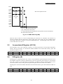
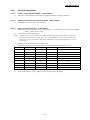
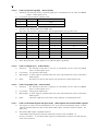
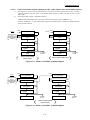
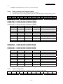
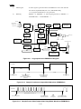
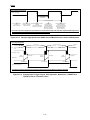
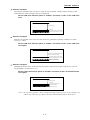
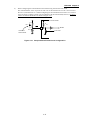
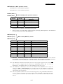
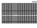
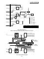
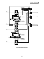
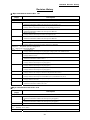
1
CMOS 8-BIT MICROCONTROLLER
LC872600 SERIES
USER’S MANUAL
http://onsemi.com
REV : 1.00
ON Semiconductor
Digital Solution Division
Microcontroller & Flash Business Unit
ON Semiconductor and the ON logo are registered trademarks of Semiconductor Components Industries, LLC (SCILLC). SCILLC owns the rights to a number
of patents, trademarks, copyrights, trade secrets, and other intellectual property. A listing of SCILLC’s product/patent coverage may be accessed at
www.onsemi.com/site/pdf/Patent-Marking.pdf. SCILLC reserves the right to make changes without further notice to any products herein. SCILLC makes no
warranty, representation or guarantee regarding the suitability of its products for any particular purpose, nor does SCILLC assume any liability arising out of the
application or use of any product or circuit, and specifically disclaims any and all liability, including without limitation special, consequential or incidental
damages. “Typical” parameters which may be provided in SCILLC data sheets and/or specifications can and do vary in different applications and actual
performance may vary over time. All operating parameters, including “Typicals” must be validated for each customer application by customer’s technical experts.
SCILLC does not convey any license under its patent rights nor the rights of others. SCILLC products are not designed, intended, or authorized for use as
components in systems intended for surgical implant into the body, or other applications intended to support or sustain life, or for any other application in which
the failure of the SCILLC product could create a situation where personal injury or death may occur. Should Buyer purchase or use SCILLC products for any
such unintended or unauthorized application, Buyer shall indemnify and hold SCILLC and its officers, employees, subsidiaries, affiliates, and distributors
harmless against all claims, costs, damages, and expenses, and reasonable attorney fees arising out of, directly or indirectly, any claim of personal injury or
death associated with such unintended or unauthorized use, even if such claim alleges that SCILLC was negligent regarding the design or manufacture of the
part. SCILLC is an Equal Opportunity/Affirmative Action Employer. This literature is subject to all applicable copyright laws and is not for resale in any manner.
Contents
Chapter 1
1.1
1.2
1.3
1.4
1.5
1.6
1.7
1.8
Overview ···································································································· 1-1
Features ····································································································· 1-1
Pinout ········································································································· 1-6
System Block Diagram ··············································································· 1-7
Pin Description ··························································································· 1-8
Port Output Types ······················································································ 1-9
Recommended Unused Pin Connections ·················································· 1-9
User Options ······························································································ 1-9
Chapter 2
2.1
2.2
2.3
2.4
2.5
2.6
2.7
2.8
2.9
2.10
2.11
Overview ·················································································· 1-1
Internal Configuration ···························································· 2-1
Memory Space ··························································································· 2-1
Program Counter (PC) ··············································································· 2-1
Program Memory (ROM)············································································ 2-2
Internal Data Memory (RAM) ····································································· 2-2
Accumulator/A Register (ACC/A) ······························································· 2-3
B Register (B) ···························································································· 2-3
C Register (C) ···························································································· 2-4
Program Status Word (PSW) ····································································· 2-4
Stack Pointer (SP)······················································································ 2-5
Indirect Addressing Registers ···································································· 2-5
Addressing Modes ····················································································· 2-6
2.11.1 Immediate Addressing (#) ······························································ 2-6
2.11.2 Indirect Register Indirect Addressing ([Rn]) ··································· 2-7
2.11.3 Indirect Register + C Register Indirect Addressing ([Rn,C]) ··········· 2-7
2.11.4 Indirect Register (R0) + Offset Value indirect Addressing ([off])····· 2-8
2.11.5 Direct Addressing (dst) ··································································· 2-8
2.11.6 ROM Table Look-up Addressing ···················································· 2-9
2.11.7 External Data Memory Addressing················································· 2-9
Chapter 3
Peripheral System Configuration ··········································· 3-1
3.1 Port 1 ··········································································································· 3-1
3.1.1 Overview ······························································································ 3-1
3.1.2 Functions ······························································································ 3-1
3.1.3 Related Registers ················································································· 3-2
3.1.4 Options ································································································· 3-6
3.1.5 HALT and HOLD Mode Operation························································ 3-6
-1-
Contents
3.2 Port 3 ··········································································································· 3-7
3.2.1 Overview ······························································································ 3-7
3.2.2 Functions ······························································································ 3-7
3.2.3 Related Registers ················································································· 3-9
3.2.4 Options ······························································································· 3-12
3.2.5 HALT and HOLD Mode Operation······················································ 3-12
3.3 Timer/Counter 0 (T0) ················································································· 3-13
3.3.1 Overview ···························································································· 3-13
3.3.2 Functions ···························································································· 3-13
3.3.3 Circuit configuration············································································ 3-15
3.3.4 Related Registers ··············································································· 3-19
3.4 Timer/Counter 1 (T1) ················································································· 3-22
3.4.1 Overview ···························································································· 3-22
3.4.2 Functions ···························································································· 3-22
3.4.3 Circuit Configuration ··········································································· 3-23
3.4.4 Related Registers ··············································································· 3-26
3.5 Serial Interface 7 (SIO7) ············································································ 3-29
3.5.1 Overview ···························································································· 3-29
3.5.2 Functions ···························································································· 3-29
3.5.3 Circuit Configuration ··········································································· 3-29
3.5.4 Related Registers ··············································································· 3-31
3.5.5 SIO7 Transmission Examples ···························································· 3-32
3.5.6 SIO7 HALT Mode Operation ······························································ 3-33
3.6 High-speed 12-bit PWM (HPWM) ······························································ 3-34
3.6.1 Overview ···························································································· 3-34
3.6.2 Functions ···························································································· 3-34
3.6.3 Circuit Configuration ··········································································· 3-35
3.6.4 Related Registers ··············································································· 3-39
3.7 High-speed Pulse Width/Period Measurement Counter 1 (HCT1)············· 3-43
3.7.1 Overview ···························································································· 3-43
3.7.2 Functions ···························································································· 3-43
3.7.3 Circuit Configuration ··········································································· 3-44
3.7.4 Related Registers ··············································································· 3-46
3.8 High-speed Pulse Width/Period Measurement Counter 2 (HCT2)············· 3-48
3.8.1 Overview ···························································································· 3-48
3.8.2 Functions ···························································································· 3-48
3.8.3 Circuit Configuration ··········································································· 3-49
-2-
Contents
3.8.4 Related Registers ··············································································· 3-53
3.9 AD Converter (ADC12) ·············································································· 3-57
3.9.1 Overview ···························································································· 3-57
3.9.2 Functions ···························································································· 3-57
3.9.3 Circuit Configuration ··········································································· 3-58
3.9.4 Related Registers ··············································································· 3-58
3.9.5 AD Conversion Example ···································································· 3-62
3.9.6 Hints on the Use of the ADC ······························································ 3-63
3.10 Analog Comparator (ACMP) ···································································· 3-65
3.10.1 Overview ·························································································· 3-65
3.10.2 Functions ·························································································· 3-65
3.10.3 Circuit Configuration ········································································· 3-65
3.10.4 Related Registers ············································································· 3-66
Chapter 4
Control Functions ···································································· 4-1
4.1 Interrupt Function ························································································ 4-1
4.1.1 Overview ······························································································ 4-1
4.1.2 Functions ······························································································ 4-1
4.1.3 Circuit Configuration ············································································· 4-2
4.1.4 Related Registers ················································································· 4-3
4.2 System Clock Generator Function ······························································· 4-5
4.2.1 Overview ······························································································ 4-5
4.2.2 Functions ······························································································ 4-5
4.2.3 Circuit Configuration ············································································· 4-6
4.2.4 Related Registers ················································································· 4-7
4.3 Standby Function······················································································· 4-10
4.3.1 Overview ···························································································· 4-10
4.3.2 Functions ···························································································· 4-10
4.3.3 Related Registers ··············································································· 4-10
4.4 Reset Function ·························································································· 4-13
4.4.1 Overview ···························································································· 4-13
4.4.2 Functions ···························································································· 4-13
4.4.3 Reset State ························································································ 4-14
4.5 Internal Reset Function ············································································· 4-15
4.5.1 Overview ···························································································· 4-15
4.5.2 Functions ···························································································· 4-15
4.5.3 Circuit Configuration ··········································································· 4-15
-3-
Contents
4.5.4 Options ······························································································· 4-16
4.5.5 Sample Operating Waveforms of the Internal Reset Circuit ··············· 4-18
4.5.6 Notes on the Use of the Internal Reset Circuit ··································· 4-19
4.5.7 Notes to be Taken When Not Using the Internal Reset Circuit ··········· 4-20
4.6 Watchdog Timer (WDT) ············································································· 4-22
4.6.1 Overview ···························································································· 4-22
4.6.2 Functions ···························································································· 4-22
4.6.3 Circuit Configuration ··········································································· 4-22
4.6.4 Related Registers ··············································································· 4-24
4.6.5 Notes on the Use of the Watchdog Timer ·········································· 4-26
Appendixes
A-I 87-Register Map ·················································································· AI-(1-4)
A-II Port Block Diagrams ··········································································· AII-(1-4)
Revision History ··························································································· R-1
-4-
LC872600 Chapter 1
1. Overview
1.1
Overview
The SANYO LC872600 series is an 8-bit microcontroller that, centered around a CPU running at a
minimum bus cycle time of 100 ns, integrate on a single chip a number of hardware features such as 8K
bytes of flash ROM (onboard programmable), 512 bytes of RAM, an on-chip debugger, two 16-bit
timer/counters (may be divided into 8-bit timers), a synchronous SIO interface, a high-speed 12-bit PWM
module, two high-speed pulse width/period measurement counters, a 3-channel AD converter with a 12-/8bit resolution selector, an analog comparator, a watchdog timer, an internal reset circuit, a system clock
frequency divider, and 16-source 10-vector interrupt feature.
1.2
●
Features
ROM
LC872600 series
LC87F2608A: 8192 × 8 bits (flash ROM)
• Onboard programmable with a wide range of supply voltages (3.0 to 5.5V)
• Block-erasable in 128-byte units
●
RAM
LC872600 series
LC87F2608A: 512 × 9 bits
●
Minimum bus cycle time
• 100 ns (10 MHz)
Note: The bus cycle time here refers to the ROM read speed.
●
Minimum instruction cycle time (Tcyc)
• 300 ns (10 MHz)
1-1
●
Ports
●
Normal withstand voltage I/O ports
Ports whose I/O direction can be designated in 1 bit units: 7 (P10 to P12, P30 to P33)
Reset pin:
1 (RES)
●
Power pins:
●
●
Timers
● Timer 0: 16-bit timer/counter with capture registers
Mode 0:
Mode 1:
Mode 2:
Mode 3:
●
8-bit timer with an 8-bit programmable prescaler (with 8-bit capture registers) × 2
channels
8-bit timer with an 8-bit programmable prescaler (with 8-bit capture registers) + 8-bit
counter (with 8-bit capture registers)
16-bit timer with an 8-bit programmable prescaler (with 16-bit capture registers)
16-bit counter (with 16-bit capture registers)
Timer 1: 16-bit timer/counter
Mode 0:
Mode 2:
●
2 (VSS1, VDD1)
8-bit timer with an 8-bit prescaler + 8-bit timer/counter with an 8-bit prescaler
16-bit timer/counter with an 8-bit prescaler
Serial interface
●
SIO7: 8-bit synchronous serial interface
1)
LSB first/MSB first mode selectable
2)
Built-in 8-bit baudrate generator (maximum transfer clock cycle =
4
3
Tcyc)
●
High-speed 12 bits PWM
• System clock or high-speed RC oscillator clock (20 MHz or 40 MHz) selectable
• Programmable duty cycle and period
• Continuous PWM output or PWM set value output (automatic stop) selectable
●
High-speed pulse width/period measurement counters
●
HCT1: High-speed pulse width/period measurement counter 1
1)
System clock or high-speed RC oscillator clock (20 MHz or 40 MHz) selectable
2)
High-level width, low-level width, or period measurement selectable
3)
Input triggering noise filter function
●
HCT2: High-speed pulse width/period measurement counter 2
1)
System clock or high-speed RC oscillator clock (20 MHz or 40 MHz) selectable
2)
Can measure the low-level width and period at the same time.
3)
Input triggering noise filter function
4)
Input trigger selectable (from P11/HCT2IN, P31/HCT2IN, and analog comparator output)
●
AD converter: 12 bits × 3 channels
• 12/8 bits AD converter resolution selectable
●
Analog comparator
• Can output data to the P32/CMPO port (output polarity selectable).
• Edge detection function (multiplexed with INTC, noise filter feature selectable)
1-2
LC872600 Chapter 1
●
Watchdog timer
• Can generate an internal reset signal on an overflow of a timer that runs on the WDT-dedicated
low-speed RC oscillator clock (30 kHz).
• Continuation, termination, or holding mode is selectable as the watchdog timer operating when the
CPU enters the HALT or HOLD mode.
●
Interrupts: 16 sources, 10 vector addresses
1)
Provides three levels (low (L), high (H), and highest (X)) of multiplex interrupt control. Any
interrupt requests of the level equal to or lower than the current interrupt are not accepted.
2)
When interrupt requests to two or more vector addresses occur at the same time, the interrupt
of the highest level takes precedence over the other interrupts. For interrupts of the same level,
the interrupt into the smallest vector address takes precedence.
1
Vector
Address
00003H
X or L
INTA
2
0000BH
X or L
INTB
3
00013H
H or L
INTC/T0L/INTE
4
0001BH
H or L
INTD/INTF
No.
Level
Interrupt Source
5
00023H
H or L
T0H/SIO7
6
0002BH
H or L
T1L/T1H
7
00033H
H or L
HCT1
8
0003BH
H or L
HCT2
9
00043H
H or L
ADC/HPWM automatic stop/HPWM period
10
0004BH
H or L
None
• Priority levels X > H > L
• Of interrupts of the same level, the one with the smallest vector address takes precedence.
●
Subroutine stack levels: 256 levels maximum (The stack is allocated in RAM.)
●
High-speed multiplication/division instructions
• 16 bits × 8 bits (5 Tcyc execution time)
• 24 bits × 16 bits (12 Tcyc execution time)
• 16 bits ÷ 8 bits (8 Tcyc execution time)
• 24 bits ÷ 16 bits (12 Tcyc execution time)
●
Oscillation circuits
• Medium-speed RC oscillation circuit (internal): For system clock (1 MHz)
• Low-speed RC oscillation circuit (internal):
For watchdog timer only (30 kHz)
• High-speed RC oscillation circuit (internal):
For system clock (20 MHz or 40 MHz)
1)
The source oscillation frequency of the high speed RC oscillation circuit can be selected from
2 sources (20 MHz and 40 MHz) by configuring options.
●
System clock frequency divider function
• Can run on low current.
• The minimum instruction cycle selectable from 300ns, 600ns, 1.2μs, 2.4μs, 4.8μs, 9.6μs, 19.2μs,
38.4μs, and 76.8μs (when high-speed RC oscillation is selected as the system clock source).
1-3
●
Internal reset circuit
● Power-on reset (POR) function
1)
2)
●
Low-voltage detection reset (LVD) function
1)
2)
●
LVD and POR functions are combined to generate resets when power is turned on and when
power voltage falls below a certain level.
The use/disuse of the LVD function and the low voltage threshold level can be selected from 3
levels (2.81V, 3.79V, and 4.28V) by configuring options.
Standby function
● HALT mode: Halts instruction execution while allowing the peripheral circuits to
continue operation.
1)
2)
●
Oscillation is not stopped automatically.
There are the following three ways of resetting the HOLD mode.
(1) Setting the Reset pin to the low level
(2) Generating a reset signal via the watchdog timer or brown-out detector
(3) Having an interrupt generated
HOLD mode: Suspends instruction execution and the operation of the peripheral
circuits.
1)
2)
●
POR reset is generated only at power-on time.
The POR release level can be selected from 3 levels (2.87V, 3.86V, and 4.35V) by configuring
options.
The medium- and high-speed RC oscillators automatically stop operation.
There are the following four ways of resetting the HALT mode.
(1) Setting the Reset pin to the low level
(2) Generating a reset signal via the watchdog timer or brown-out detector
(3) Setting at least one of the INTA, INTB, INTC, INTD, INTE, and INTF pins to the
specified level (INTA and INTB HOLD mode reset is available only when level
detection is set.)
(4) Applying input signals to the IN+ and IN- pins so that the analog comparator output is
set to the specified level (when the analog comparator output is assigned to the INTC
input)
On-chip Debugger Function
• Supports software debugging with the IC mounted on the target board (selectable from 3 series).
1) LC87D2708A : All terminal function of LC87F2608A can be used.
2) LC87F2708A : All terminal function of LC87F2608A can be used. The debug feature is limited.
3) LC87F2608A : The debugger terminal function when an On-chip debugger is used cannot be
used. The debug feature is limited.
• Two channels of on-chip debugger pins are available (LC87F2608A).
1-4
LC872600 Chapter 1
●
Data security feature
・Protects the program data stored in flash memory from unauthorized read or copy.
Note: This data security feature does not necessarily provide absolute data security.
●
Package Form
• MFP10S
(Lead-/Halogen-free type)
• MFP14S (for debugging only) (Lead-free type)
●
Development tools
• On-chip debugger: 1)
2)
3)
4)
TCB87-Type B + LC87D2708A or LC87F2708A
TCB87-Type B + LC87F2608A
TCB87-Type C (3 wire version) + LC87D2708A or LC87F2708A
TCB87-Type C (3 wire version) + LC87F2608A
1-5
1.3
Pinout
P31/INTB/HCT2IN/DBGP01
1
10
P30/INTA/HCT1IN/DBGPX0
2
9
P32/INTC/CMPO/DBGP11
RES
3
8
P33/INTD/HPWM/DBGP12
P10/SO7/INTE/AN0/DBGP02
4
7
P11/SI7/SB7/INTE/IN+/HCT2IN/AN1
VSS1
5
6
P12/SCK7/INTF/IN-/AN2
VDD1
SANYO: MFP10S (Lead-/Halogen-free type)
P31/INTB/HCT2IN/DBGP01
1
14
VDD1
P30/INTA/HCT1IN/DBGPX0
2
13
P32/INTC/CMPO/DBGP11
RES
3
12
P33/INTD/HPWM/DBGP12
P10/SO7/INTE/AN0/DBGP02
4
11
P11/SI7/SB7/INTE/IN+/HCT2IN/AN1
VSS1
5
10
P12/SCK7/INTF/IN-/AN2
NC
6
9
DBGP20
DBGP22
7
8
DBGP21
SANYO: MFP14S (for debugging only) (Lead-free type)
1-6
LC872600 Chapter 1
System Block Diagram
Interrupt control
IR
Standby control
PLA
Flash ROM
Hi-speed
RC
Freq. divider
Mediumspeed RC
Clock
generator
PC
RES#
ACC
WDT
Reset
(Low-speed RC) control
Reset circuit
(LVD/POR)
Bus interface
Timer 0
Port 1
(INTE to INTF)
Timer 1
Port 3
(INTA to INTD)
Hi-speed PWM
Data bus
B register
SIO7
Data bus
1.4
C register
ALU
PSW
ADC
RAR
HCT1
HCT2
RAM
Analog
comparator
Stack pointer
On-chip debugger
1-7
1.5
Pin Description
Name
VSS1
VDD1
Port 1
P10 to P12
I/O
−
− power supply
Option
No
−
+ power supply
No
• 3-bit I/O port
• I/O specifiable in 1-bit units
• Pull-up resistors can be turned on and off in 1-bit units.
• Multiplexed pin functions
P10: SIO7 data output/
INTE input/HOLD release input/timer 1 event input/
timer 0L capture input/timer 0H capture input
P11: SIO7 data input/bus I/O/
high-speed pulse width-period measurement counter 2
input/INTE input/HOLD release input/timer 1 event input/
timer 0L capture input/timer 0H capture input
P12: SIO7 clock I/O/
INTF input/HOLD release input/timer 1 event input/
timer 0L capture input/timer 0H capture input
AD converter input ports: AN0 to AN2
Analog comparator input port: IN +, IN −
On-chip debugger pin 1: DBGP02
• Interrupt acknowledge type
Yes
I/O
Description
INTE
INTF
Port 3
P30 to P33
I/O
I/O
Falling
Rising
&
Falling
H level
L level
○
○
○
○
○
○
×
×
×
×
• 4-bit I/O port
• I/O specifiable in 1-bit units
• Pull-up resistors can be turned on and off in 1-bit units.
• Multiplexed pin functions
P30: INTA input/HOLD release input/timer 0L capture input/
high-speed pulse width-period measurement counter 1 input
P31: INTB input/HOLD release input/timer 0H capture input/
high-speed pulse width-period measurement counter 2 input
P32: INTC input/HOLD release input/timer 0 event input/
timer 0L capture input/analog comparator output
P33: INTD input/HOLD release input/timer 0 event input/
timer 0H capture input/high-speed PWM output
On-chip debugger pin 1: DBGPX0 to DBGP01
On-chip debugger pin 2: DBGPX0 to DBGP12
• Interrupt acknowledge type
INTA
INTB
INTC
INTD
RES
Rising
Rising
Falling
Rising
&
Falling
H level
L level
○
○
○
○
○
○
○
○
×
×
○
○
○
○
×
×
○
○
×
×
External reset input/internal reset output
1-8
Yes
No
LC872600 Chapter 1
1.6
Port Output Types
The table below lists the types of port outputs and the presence/absence of a pull-up resistor. Data can be
read from an input/output port even if it is in the output mode.
Port Name
Option
Selection
Unit
P10 to P12
1 bit
P30 to P33
1 bit
1.7
Output Type
Pull-up Resistor
1
CMOS
Programmable
2
N-channel open drain
Programmable
1
CMOS
Programmable
2
N-channel open drain
Programmable
Recommended Unused Pin Connections
Recommended Unused Pin Connections
Board
Software
Set output low
Pin Name
P10 to P12
OPEN
P30 to P33
OPEN
1.8
Option
Type
Set output low
User Options
Option Name
Option Type
Flash
Version
Options
Switched in
Units of
P10 to P12
○
1 bit
P30 to P33
○
1 bit
-
○
-
○
-
○
-
3 levels
Power-on-reset
level
○
-
3 levels
Oscillation
frequency
○
-
Port output type
Program start address
Brown-out
detector
function
Brown-out detector reset
function
Brown-out trip
level
Power-on-reset
function
High-speed RC oscillator
circuit
Description
CMOS
N-channel open drain type
CMOS
N-channel open drain type
00000H
01E00H
Enable: Used
Disable: Not used
20 MHz
40 MHz
MFP10S: LC87F2608A
Package type
-
○
1-9
-
MFP14S: Debugged by using
LC87D2708A or LC87F2708A
1-10
LC872600 Chapter 2
2.
Internal Configuration
2.1
Memory Space
This series of microcontrollers have the following three types of memory space:
1)
2)
Program memory space:
Internal data memory space:
3)
External data memory space:
Address
256K bytes (128K bytes × 2 banks)
64K bytes (0000H to FDFFH out of 0000H to FFFFH is shared
with the stack area.)
16M bytes
External data memory space
Program memory space
Address
FFFFFFH
3FFFFH
ROM bank 1
128KB
Intermal data
memory space
Address
FFFFH
FF00H
FEFFH
SFR(8-bit)
1FFFFH
ROM bank 0
128KB
RAM
16MB
Reserved for
system
(some 9-bit)
FE00H
FDFFH
RAM/Stack
64 KB
(9-bit config)
00000H
000000H
0000H
Note: SFR is the area in which special registers such as the accumulator are allocated (see
Appendixes A-I).
Figure 2.1.1 Types of Memory Space
2.2
Program Counter (PC)
The program counter (PC) is made up of 17 bits and a bank flag BNK. The value of BNK determines the
bank. The lower-order 17 bits of the PC allows linear access to the 128K ROM space in the current bank.
Normally, the PC advances automatically in the current bank on each execution of an instruction. Bank
switching is accomplished by executing a Return instruction after pushing necessary addresses onto the
stack. When executing a branch or subroutine instruction, when accepting an interrupt, or when a reset is
generated, the value corresponding to each operation is loaded into the PC.
Table 2.2.1 lists the values that are loaded into the PC when the respective operations are performed.
2-1
Table 2.2.1
Values Loaded in the PC
Operation
PC value
Inter- Reset
00000H
BNK value
0
rupt
INTA
00003H
0
INTB
0000BH
0
INTC/T0L/INTE
00013H
0
INTD/INTF
0001BH
0
T0H/SIO7
00023H
0
T1L/T1H
0002BH
0
HCT1
00033H
0
HCT2
0003BH
0
ADC/HPWM automatic stop/HPWM period
00043H
0
None
0004BH
0
Unconditional branch
instructions
JUMP
a17
PC=a17
Unchanged
BR
r12
PC=PC+2+r12[-2048 to +2047]
Unchanged
Conditional branch
instructions
BE, BNE, DBNZ, DBZ, BZ, BNZ,
BZW, BNZW, BP, BN, BPC
PC=PC+nb+r8[-128 to +127]
nb: Number of instruction bytes
Unchanged
Call instructions
CALL
PC=a17
Unchanged
RCALL r12
PC=PC+2+r12[-2048 to +2047]
Unchanged
RCALLA
PC=PC+1+Areg[0 to +255]
Unchanged
Return instructions
RET, RETI
PC16 to 08=(SP)
BNK is set
PC07 to 00=(SP-1)
to bit 8 of
(SP) denotes the contents of RAM (SP-1).
address designated by the value of
the stack pointer SP.
Standard instructions
NOP, MOV, ADD, …
PC=PC+nb
nb: Number of instruction bytes
2.3
a17
Unchanged
Program Memory (ROM)
This series of microcontrollers have a program memory space of 256K bytes but the size of the ROM that
is actually incorporated in the microcontroller varies with the CPU type of the microcontroller. The ROM
table lookup instruction (LDCW) can be used to refer all ROM data within the bank. Of the ROM space,
the 256 bytes in ROM bank 0 (01F00H-01FFFH for this series of microcontrollers) are reserved as the
option area. Consequently, this area is not available as a program area.
2.4
Internal Data Memory (RAM)
The LC870000 series microcontrollers have an internal data memory space of 64K bytes but the size of the
RAM that is actually incorporated in the microcontroller varies with the series of the microcontroller. 9
bits are used to access addresses 0000H to FDFFH of the 128K ROM space and 8 or 9 bits are used to
access addresses FE00H to FFFFH. The 9th bit of RAM is implemented by bit 1 of the PSW and can be
read and written.
The 128 bytes of RAM from 0000H to 007FH are paired to form 64 2-byte and can also be used as 64
indirect address registers. The bit length of these indirect registers is normally 16 bits (8 bits × 2). When
they are used by the ROM table lookup instruction (LDCW), however, their bit length is set to 17 bits (9
higher-order bits + 8 lower-order bits).
As shown in Figure 2.4.1, the usable instructions vary depending on the address of RAM.
The efficiency improvement of use ROM and execution speed can be attempted by using these instructions
properly.
2-2
LC872600 Chapter 2
FFFFH
Reserved for
system
FF00H
FEFFH
FE00H
FDFFH
2000H
1FFFH
*Note: Some registers are 9-bit
SFR space
* 8-bit
RAM/
Stack space
9-bit
0200H
01FFH
0100H
00FFH
0000H
Bit instruction direct (long)
Bit instruction direct (short)
Non-bit instruction direct (long)/indirect,16-bit operation instruction direct/indirect
Non-bit instruction direct (short)
Fig. 2.4.1 RAM Addressing Map
When the value of the PC is stored in RAM during the execution of a subroutine call instruction or
interrupt, assuming that SP represents the current value of the stack pointer, the value of BNK and the
lower-order 8 bits of the (17-bit) PC are stored in RAM address SP + 1 and the higher-order 9 bits in SP +
2, after which SP is set to SP + 2.
2.5
Accumulator/A Register (ACC/A)
The accumulator (ACC), also called the A register, is an 8-bit register that is used for data computation,
transfer, and I/O processing. It is allocated to address FE00H in the internal data memory space and
initialized to 00H on a reset.
Address
Initial value
R/W
Name
BIT7
BIT6
BIT5
BIT4
BIT3
BIT2
BIT1
BIT0
FE00
0000 0000
R/W
AREG
AREG7
AREG6
AREG5
AREG4
AREG3
AREG2
AREG1
AREG0
2.6
B Register (B)
The B register is combined with the ACC to form a 16-bit arithmetic register during the execution of a 16bit arithmetic instruction. During a multiplication or division instruction, the B register is used with the
ACC and C register to store the results of computation. In addition, during an external memory access
instruction (LDX or STX), the B register designates the higher-order 8 bits of the 24-bit address.
The B register is allocated to address FE01H of the internal data memory space and initialized to 00H on a
reset.
Address
Initial value
R/W
Name
BIT7
BIT6
BIT5
BIT4
BIT3
BIT2
BIT1
BIT0
FE01
0000 0000
R/W
BREG
BREG7
BREG6
BREG5
BREG4
BREG3
BREG2
BREG1
BREG0
2-3
2.7
C Register (C)
The C register is used with the ACC and B register to store the results of computation during the execution
of a multiplication or division instruction. In addition, during a C register offset indirect instruction, the C
register stores the offset data (-128 to + 127) to the contents of an indirect register.
The C register is allocated to address FE02H of the internal data memory space and initialized to 00H on a
reset.
Address
Initial value
R/W
Name
BIT7
BIT6
BIT5
BIT4
BIT3
BIT2
BIT1
BIT0
FE02
0000 0000
R/W
CREG
CREG7
CREG6
CREG5
CREG4
CREG3
CREG2
CREG1
CREG0
2.8
Program Status Word (PSW)
The program status word (PSW) is made up of flags that indicate the status of computation results, a flag
to access the 9th bit of RAM, and a flag to designate the bank during the LDCW instruction. The PSW is
allocated to address FE06H of the internal data memory space and initialized to 00H on a reset.
Address
Initial value
R/W
Name
BIT7
BIT6
BIT5
BIT4
BIT3
BIT2
BIT1
BIT0
FE06
0000 0000
R/W
PSW
CY
AC
PSWB5
PSWB4
LDCBNK
OV
P1
PARITY
CY (bit 7): Carry flag
CY is set (to 1) when a carry occurs as the result of a computation and cleared (to 0) when no carry occurs.
There are the following types of carries:
1)
2)
3)
4)
Carry resulting from an addition
Borrow resulting from a subtraction
Borrow resulting from a comparison
Carry resulting from a rotation
There are some instructions that do not affect this flag at all.
AC (bit 6): Auxiliary carry flag
AC is set (to 1) when a carry or borrow occurs in bit 3 (bit 3 of the higher-order byte during a 16-bit
computation) as the result of an addition or subtraction and cleared (to 0) otherwise.
There are some instructions that do not affect this flag at all.
PSWB5, PSWB4 (bits 5 and 4): User bits
These bits can be read and written through instructions. They can be used by the user freely.
LDCBNK (bit 3): Bank flag for the table lookup instruction (LDCW)
This bit designates the ROM bank to be specified when reading the program ROM with a table lookup
instruction.
(0: ROM-ADR = 0 to 1FFFF, 1: ROM-ADR = 20000 to 3FFFF)
OV (bit 2): Overflow flag
OV is set (to 1) when an overflow occurs as the result of an arithmetic operation and cleared (to 0)
otherwise. An overflow occurs in the following cases:
1)
2)
When MSB is used as the sign bit and when the result of negative number + negative number or
negative number – positive number is a positive
When MSB is used as the sign bit and when the result of positive number + positive number or
positive number – negative number is a negative number
2-4
LC872600 Chapter 2
3)
4)
5)
When the higher-order 8 bits of a 16 bits × 8 bits multiplication is nonzero
When the higher-order 16 bits of a 24 bits × 16 bits multiplication is nonzero
When the divisor of a division is 0
There are some instructions that do not affect this flag at all.
P1 (bit 1): RAM bit 8 data flag
P1 is used to manipulate bit 8 of 9-bit internal data RAM (0000H to FDFFH). Its behavior varies
depending on the instruction executed. See Table 2-4-2 for details.
PARITY (bit 0): Parity flag
This bit shows the parity of the accumulator (A register). The parity flag is set (to 1) when there are an odd
number of 1s in the A register. It is cleared (to 0) when there are an even number of 1s in the A register.
2.9
Stack Pointer (SP)
The LC870000 series microcontrollers can use RAM addresses 0000H to FDFFH as a stack area. The size
of RAM, however, varies depending on the model of the microcontroller. The SP is 16 bits long and made
up of two registers: SPL (at address FE0A) and SPH (at address FE0B). It is initialized to 0000H on a reset.
The SP is incremented by 1 before data is saved in stack memory and decremented by 1 after the data is
restored from stack memory.
Address
Initial value
R/W
Name
BIT7
BIT6
BIT5
BIT4
FE0A
0000 0000
R/W
SPL
SP7
SP6
SP5
SP4
FE0B
0000 0000
R/W
SPH
SP15
SP14
SP13
SP12
BIT3
BIT2
BIT1
BIT0
SP3
SP2
SP1
SP0
SP11
SP10
SP9
SP8
The value of the SP changes as follows:
1)
2)
3)
4)
2.10
When the PUSH instruction is executed: SP = SP + 1, RAM (SP) = DATA
When the CALL instruction is executed: SP = SP + 1, RAM (SP) = ROMBANK + ADL
SP = SP + 1, RAM (SP) = ADH
When the POP instruction is executed: DATA = RAM (SP), SP = SP - 1
When the RET instruction is executed: ADH = RAM (SP), SP = SP - 1
ROM BANK + ADL = RAM(SP), SP = SP - 1
Indirect Addressing Registers
The LC870000 series microcontrollers are provided with three addressing schemes ([Rn], [Rn + C], [off])
that use the contents of indirect registers (indirect addressing modes). (See Section 2.11 for the addressing
modes.) Used for these addressing modes are 64 2-byte indirect registers (R0 to R63) allocated to RAM
addresses 0 to 7EH. The indirect registers can also be used as general-purpose registers (e.g., for saving 2byte data). Naturally, these addresses can be used as ordinary RAM (on a 1 byte (9 bits) basis) if they are
not used as indirect registers. R0 to R63 are "system reserved words" to the assembler and need not be
defined by the user.
2-5
RAM
Reserved for system
Address
・
7FH
R63(upper)
7EH
R63(lower)
・
・
・
・
・
・
03H
R1(upper)
02H
R1(lower)
01H
R0(upper)
00H
R0(lower)
R63=7EH
R1=2
R0=0
Fig. 2.10.1 Allocation of Indirect Registers
2.11
Addressing Modes
The LC870000 series microcontrollers support the following seven addressing modes:
1)
2)
3)
4)
5)
6)
7)
Immediate (immediate data refers to data whose value has been established at program preparation
(assembly) time.)
Indirect register (Rn) indirect (0 ≦ n ≦ 63)
Indirect register (Rn) + C register indirect (0 ≦ n ≦ 63)
Indirect register (R0) + Offset value indirect
Direct
ROM table look-up
External data memory access
The rest of this section describes these addressing modes.
2.11.1
Immediate Addressing (#)
The immediate addressing mode allows 8-bite (1-byte) or 16-bit (1-word) immediate data to be handled.
Examples are given below.
Examples:
LD
L1: LDW
PUSH
ADD
BE
#12H
#1234H
#34H
#56H
#78H, L1
;Loads the accumulator with byte data (12H).
;Loads the BA register pair with word data (1234H).
;Loads the stack with byte data (34H).
;Adds byte data (56H) to the accumulator.
;Compares byte data (78H) with the accumulator for a branch.
2-6
LC872600 Chapter 2
2.11.2
Indirect Register Indirect Addressing ([Rn])
In the indirect register indirect addressing mode, it is possible to select one of the indirect registers (R0 to
R63) and use its contents to designate an address in RAM or SFR. When the selected register contains, for
example, "FE02H," it designates the C register.
Example: When R3 contains "123H" (RAM address 6: 23H, RAM address 7: 01H)
LD
[R3]
;Transfers the contents of RAM address 123H to the accumulator.
L1: STW
[R3]
;Transfers the contents of BA register pair to RAM address 123H.
PUSH [R3]
;Saves the contents of RAM address123H in the stack.
SUB
[R3]
;Subtracts the contents of RAM address 123H from the accumulator.
DBZ
[R3], L1
;Decrements the contents of RAM address 123H by 1 and causes a branch if
zero.
2.11.3
Indirect Register + C Register Indirect Addressing ([Rn, C])
In the indirect register + C register indirect addressing mode, the result of adding the contents of one of the
indirect registers (R0 to R63) to the contents of the C register (-128 to + 127 with MSB being the sign bit)
designates an address in RAM or SFR. For example, if the selected indirect register contains "FE02H" and
the C register contains "FFH (-1)," the address "B register (FE02H + (-1) = FE01H" is designated.
Examples: When R3 contains "123H" and the C register contains "02H"
LD
[R3, C]
;Transfers the contents of RAM address 125H to the accumulator.
L1: STW
[R3, C]
;Transfers the contents of the BA register pair to RAM address 125H.
PUSH [R3, C]
;Saves the contents of 125H in the stack.
SUB
[R3, C]
;Subtracts the contents of RAM address 125H from the accumulator.
DBZ
[R3, C], L1 ;Decrements the contents of RAM address 125H by 1 and causes a branch if
zero.
<Notes on this addressing mode>
The internal data memory space is divided into three closed functional areas as explained in Section 2.1,
namely, 1) system reserved area (FF00H to FFFFH), 2) SFR area (FE00H to FEFFH), and 3) RAM/stack
area (0000H to FDFFH). Consequently, it is disallowed to point to a different area using the value of the C
register from the basic area designated by the contents of Rn. For example, if the instruction "LD [R5,C]"
is executed when R5 contains "0FDFFH" and the C register contains "1," since the basic area is 3)
RAM/stack area (0000H to FDFFH), the intended address "0FDFFH + 1 = 0FE00H" lies outside the basic
area and "0FFH" is consequently placed in the ACC. If the instruction "LD [R5,C]" is executed when R5
contains "0FEFFH" and the C register contains "2," since the basic area is 2) SFR area (FE00H to FEFFH),
the intended address "0FEFFH + 2 = 0FF01H" lies outside the basic area. In this case, since SFR is
confined in an 8-bit address space, the part of the address data addressing outside the 8-bit address space is
ignored and the contents of 0FE01H (B register) are placed in the ACC as the result of the computation
"0FF01H&0FFH + 0FE00H = 0FE01H"
2-7
2.11.4
Indirect Register (R0) + Offset Value indirect Addressing ([off])
In this addressing mode, the results of adding the 7-bit signed offset data off (-64 to + 63) to the contents
of the indirect register R0 designate an address in RAM or SFR. If R0 contains "FE02H" and off has a
value of "7EH(-2)," for example, the A register (FE02H + (-2) = FE00H) is designated.
Examples: When R0 contains "123H" (RAM address 0: 23H, RAM address 1: 01H)
LD
[10H]
;Transfers the contents of RAM address 133H to the accumulator.
L1: STW
[10H]
;Transfers the contents of the BA register pair to RAM address 133H.
PUSH [10H]
;Saves the contents of RAM address 133H in the stack.
SUB
[10H]
;Subtracts the contents of RAM address 133H from the accumulator.
DBZ
[10H], L1
;Decrements the contents of RAM address 133H by 1 and causes a branch if
zero.
<Notes on this addressing mode>
The internal data memory space is divided into three closed functional areas as explained in Section 2.1,
namely, 1) system reserved area (FF00H to FFFFH), 2) SFR area (FE00H to FEFFH), and 3) RAM/stack
area (0000H to FDFFH). Consequently, it is disallowed to point to a different area using an offset value
from the basic area designated by the contents of R0. For example, if the instruction "LD [1]" is executed
when R0 contains "0FDFFH," since the basic area is 3) RAM/stack area (0000H to FDFFH), the intended
address "0FDFFH + 1 = 0FE00H" lies outside the basic area and "0FFH" is placed in the ACC as the
results of LD. If the instruction "LD [2]" is executed when R0 contains "0FEFFH," since the basic area is
2) SFR (FE00H to FEFFH), the intended address "0FEFFH + 2 = 0FF01H" lies outside the basic area. In
this case, since SFR is confined in an 8-bit address space, the part of the address data addressing outside
the 8-bit address space is ignored and the contents of "0FE01H (B register) are placed in the ACC as the
result of computation "0FF01H&0FFH + 0FE00H = 0FE01H."
2.11.5
Direct Addressing (dst)
The direct addressing mode allows a RAM or SFR address to be specified directly in an operand. In this
addressing mode, the assembler automatically generates optimum instruction code from the address
specified in the operand (the number of instruction bytes varies according to the address specified in the
operand). Long (middle) range instructions (identified by an "L (M)" at the end of the mnemonic) are
available to make the byte count of instructions constant (align instructions with the longest one).
Examples:
LD
123H
LDL
123H
STW
PUSH
SUB
DBZ
123H
123H
123H
123H, L1
L1:
;Transfers the contents of RAM address 123H to the accumulator
(2-byte instruction).
;Transfers the contents of RAM address 123H to the accumulator
(3-byte instruction).
;Transfers the contents of the BA register pair to RAM address 123H.
;Saves the contents of RAM address 123H in the stack.
;Subtracts the contents of RAM address 123H from the accumulator.
;Decrements the contents of RAM address 123H by 1 and causes a branch if
zero.
2-8
LC872600 Chapter 2
2.11.6
ROM Table Look-up Addressing
The LC870000 series microcontrollers can read 2-byte data into the BA register pair at once using the
LDCW instruction. Three addressing modes [Rn], [Rn, C], and [off] are available for this purpose. (In this
case only, Rn are configured as 17-bit registers (128K-byte space)).
For models with banked ROM, it is possible to reference the ROM data in the ROM bank (128K bytes)
identified by the LDCBNK flag (bit 3) in the PSW. Consequently, when looking into the ROM table on a
series model with banked ROM, execute the LDCW instruction after switching the bank using the SET1 or
CLR1 instruction so that the LDCBNK flag designates the ROM bank where the ROM table resides.
Examples:
TBL: DB
DB
DW
•
•
LDW
CHGP3
CHGP1
STW
LDCW
MOV
LDCW
INC
LDCW
34H
12H
5678H
•
•
#TBL
(TBL >> 17) & 1
(TBL >> 16) & 1
R0
[1]
#1, C
[R0, C]
C
[R0, C]
;Loads the BA register pair with the TBL address.
;Loads LDCBNK in PSW with bit 17 of the TBL address. (Note 1)
;Loads P1 in PSW with bit 16 of the TBL address.
;Load indirect register R0 with the TBL address (bits 16 to 0).
;Reads the ROM table (B = 78H, ACC = 12H).
;Loads the C register with "01H."
;Reads the ROM table (B = 78H, ACC = 12H).
;Increments the C register by 1.
;Reads the ROM table (B = 56H, ACC = 78H).
Note 1: LDCBNK (bit 3) of PSW need to be set up only for models with banked ROM.
2.11.7
External Data Memory Addressing
The LC870000 series microcontrollers can access external data memory spaces of up to 16M bytes (24
bits) using the LDX and STX instructions. To designate a 24-bit space, specify the contents of the B
register (8 bits) as the highest-order byte of the address and the contents (16 bits) of (Rn), (Rn) + (C), or
(R0) + off (either one) as the lower-order bytes of the address.
Examples:
LDW
STW
MOV
LDX
#3456H
R0
#12H, B
[1]
;Sets up the lower-order 16 bits.
;Loads the indirect register R0 with the lower-order 16 bits of the address.
;Sets up the higher-order 8 bits of the address.
;Transfers the contents of external data memory (address 123457H) to the
accumulator.
2-9
Table 2.4.2
Chart of State Transitions of Bit 8 (RAM / SFR) and P1
Instruction
BIT8 (RAM/SFR)
P1 (PSW BIT 1)
LD#/LDW# –
–
LD
–
P1←REG8
Remarks
LDW
–
P1←REGH8
ST
REG8←P1
–
STW
REGL8, REGH8←P1
–
MOV
REG8←P1
–
PUSH#
RAM8←P1
–
PUSH
RAM8←REG8
P1←REG8
PUSHW
RAMH8←REGH8, RAML8←REGL8
P1←REGH8
PUSH_P
RAM8←Pl
–
PUSH_BA
RAMH8←P1, RAML8←P1
–
POP
REG8←RAM8
P1←RAM8
P1←bit1 when PSW is
popped
POPW
REGH8←RAMH8, REGL8←RAML8
Pl←RAMH8
P1←bit1 when higherorder address of PSW is
popped
POP_P
–
P1←RAMl (bit l)
BIT8 ignored
POP_BA
–
P1←RAMH8
XCH
REG8↔P1
Same as left.
XCHW
REGH8←P1, REGL8←Pl, P1←REGH8
Same as left.
INC
INC 9 bits
P1←REG8 after
computation
INC 9 bits
INCW
INC 17 bits, REGL8←lower byte of CY
P1←REGH8 after
computation
INC 17 bits
DEC
DEC 9 bits
P1←REG8 after
computation
DEC 9 bits
DECW
DEC 17 bits, REGL8← lower byte of CY
inverted
P1←REGH8 after
computation
DEC 17 bits
DBNZ
DEC 9 bits
P1←REG8
DEC 9 bits, check
lower-order 8 bits
DBZ
DEC 9 bits
P1←REG8
DEC 9 bits, check
lower-order 8 bits
SET1
–
–
NOT1
–
–
CLR1
–
–
BPC
–
–
BP
–
–
BN
–
–
MUL24
/DIV24
RAM8←"1"
–
FUNC
–
–
Bit 8 of RAM address
for storing results is set
to 1.
Note: A "1" is read if the processing target is an 8-bit register (no bit 8).
Legends:
REG8:
Bit 8 of a RAM or SFR location
REGH8/REGL8:
Bit 8 of the higher-order byte of a RAM location or SFR/bit 8 of the lower-order byte
RAM8:
Bit 8 of a RAM location
RAMH8/RAML8: Bit 8 of the higher-order byte of a RAM location/bit 8 of the lower-order byte
2-10
LC872600 Chapter 3
3. Peripheral System Configuration
This chapter describes the built-in functional blocks (peripheral system) of this series microcontrollers
except the CPU core, RAM, and ROM. Port block diagrams are provided in Appendix A-II for reference.
3.1
Port 1
3.1.1
Overview
Port 1 is a 3-bit I/O port equipped with programmable pull-up resistors. It is made up of a data latch, a data
direction register, a function control register, and a control circuit. Control of the input/output signal
direction is accomplished by the data direction register on a bit basis. Port 1 can also be used as a serial
interface I/O port by manipulating its function control register.
Port 1 can also serve as an input port for external interrupts. It can also be used as an input port for the timer
1 count clock, timer 0 capture signal, or HOLD mode release signal.
As a user option, either CMOS output with a programmable pull-up resistor or N-channel open drain output
with a programmable pull-up resistor can be selected as the output type on a bit basis.
Note: Port P10 is equipped temporarily with an internal pull-up resistor when the microcontroller is
reset. Do not apply a clock or intermediate level voltage to port P10 while the reset sequence
is in progress.
3.1.2
Functions
1)
I/O port (3 bits: P10 to P12)
• The port output data is controlled by the port 1 data latch (P1: FE44) and the I/O
direction is controlled by the port 1 data direction register (P1DDR: FE45).
• Each port bit is provided with a programmable pull-up resistor.
2)
Multiplexed pin function
• P11 is also used as the HCT2 input, and P12 to P10 for SIO7 I/O.
3)
Interrupt input pin functions
• One port (INTE) selected out of ports P10 and P11 and the port P12(INTF) are assigned
the pin interrupt function. They are used to sense the low, high, or both edges of an
interrupt request signal and set the corresponding interrupt flag. These two ports that are
selected can also be used as timer 1 count clock input or timer 0 capture signal input.
4)
HOLD mode release function
• When both of the interrupt flag and interrupt enable flag are set by INTE or INTF, a
HOLD mode release signal is generated, causing the CPU to switch from HOLD mode
to HALT mode (system clock assigned to intermediate-speed RC oscillation). When the
interrupt request is accepted, the CPU switches from HALT mode to normal operating
mode.
3-1
PORTS
• When a signal change such that an interrupt flag is set is input to INTE or INTF in the
HOLD mode, the interrupt flag is set. In this case, the CPU exits the HOLD mode if the
corresponding interrupt enable flag is set.
The interrupt flag, however, cannot be set by a rising edge occurring when INTE or
INTF data which is established when the HOLD mode is entered is in the high state or
by a falling edge occurring when INTE or INTF data which is established when the
HOLD mode is entered is in the low state. Consequently, to release the HOLD mode
with INTE or INTF, it is recommended that INTE or INTF be used in the both edge
interrupt mode.
5)
Analog comparator voltage input function
• The analog voltage inputs to the analog comparator are supplied from P11, P12.
6)
AD converter voltage input function
• The analog voltages to the AD converter are supplied from P10 to P12.
Address
Initial value
R/W
Name
BIT7
BIT6
BIT5
BIT4
BIT3
FE44
HHHH H000
FE45
HHHH H000
BIT2
BIT1
BIT0
R/W
P1
-
-
-
-
-
R/W
P1DDR
-
-
-
-
-
P12DDR P11DDR P10DDR
P12
P11
P10
FE46
HHHH H000
R/W
P1FCR
-
-
-
-
-
P12FCR
P11FCR
FE47
0H0H HHH0
R/W
P1TST
FIX0
-
FIX0
-
-
-
-
FE4A
0000 0000
R/W
IEFCR
FE4B
0000 0000
R/W
IEFSL
INTFHEG INTFLEG INTFIF
FIX0
FIX0
IFSL1
P10FCR
FIX0
INTFIE INTEHEG INTELEG INTEIF
INTEIE
IFSL0
IESL0
FIX0
IESL2
IESL1
* Bits 7, 5, and 0 of P1TST (FE47) are available for test purposes. They must always be set to 0.
3.1.3
Related Registers
3.1.3.1
1)
2)
Port 1 data latch (P1)
The port 1 data latch is a 3-bit register used to control the port 1 output data and pull-up registers.
When this register is read with an instruction, data at pins P10 to P12 is read in. If P1 (FE44) is
manipulated with an instruction NOT1, CLR1, SET1, DBZ, DBNZ, INC, or DEC, the contents of the
register are referenced instead of the data at port pins.
Port 1 data can always be read regardless of the I/O state of the port.
3)
Address
Initial value
R/W
Name
BIT7
BIT6
BIT5
BIT4
BIT3
BIT2
BIT1
BIT0
FE44
HHHH H000
R/W
P1
-
-
-
-
-
P12
P11
P10
3.1.3.2
1)
2)
Port 1 data direction register (P1DDR)
The port 1 data direction register is a 3-bit register that controls the I/O direction of port 1 data on a
bit basis. Port P1n are placed in the output mode when bit P1nDDR is set to 1 and in the input mode
when bit P1nDDR is set to 0.
Port P1n becomes an input with a pull-up resistor if bit P1nDDR is set to 0 and the bit P1n of the port
1 data latch is set to 1.
Address
Initial value
R/W
Name
BIT7
BIT6
BIT5
BIT4
BIT3
FE45
HHHH H000
R/W
P1DDR
-
-
-
-
-
3-2
BIT2
BIT1
BIT0
P12DDR P11DDR P10DDR
LC872600 Chapter 3
Register Data
Port P1n State
P1n
P1nDDR Input
Output
0
0
Enabled Open
1
0
Enabled Internal pull-up resistor
0
1
Enabled Low
1
1
3.1.3.3
1)
Built-in Pull-up
Resister
OFF
ON
OFF
Enabled High/open (CMOS/N-channel open drain)
OFF
Port 1 function control register (P1FCR)
The port 1 function control register is a 3-bit register that controls the multiplexed pin outputs of port
1.
Address
Initial value
R/W
Name
BIT7
BIT6
BIT5
BIT4
BIT3
BIT2
BIT1
BIT0
FE46
HHHH H000
R/W
P1FCR
-
-
-
-
-
P12FCR
P11FCR
P10FCR
n
P1nFCR
0
P1n
–
2
1
0
SIO7 clock output data
1
1
High output
0
–
Value of port data latch (P11)
1
0
SIO7 output data
1
1
High output
0
–
Value of port data latch (P10)
1
0
SIO7 output data
1
1
High output
1
0
P1n Pin Data in Output Mode (P1nDDR=1)
Value of port data latch (P12)
The high data output at a pin that is selected as an N-channel open drain output (through a user option) is
represented by an open circuit.
P12FCR (bit 2): P12 function control (SIO7 clock output control)
This bit controls the output data at pin P12.
When P12 is placed in the output mode (P12DDR = 1) and P12FCR is set to 1, the OR of the SIO7 clock
output data and the port data latch data is placed at pin P12.
P11FCR (bit 1): P11 function control (SIO7 data output control)
This bit controls the output data at pin P11.
When bit P11 is placed in the output mode (P11DDR = 1) and P11FCR is set to 1, the OR of the SIO7
output data and the port data latch data is placed at pin P11.
If SIO7 is active, SIO7 input data is taken in from pin P11 regardless of the I/O mode of P11.
P10FCR (bit 0): P10 function control (SIO7 data output control)
This bit controls the output data at pin P10.
When bit P10 is placed in the output mode (P10DDR = 1) and P10FCR is set to 1, the OR of the SIO7
output data and the port data latch data is placed at pin P10.
3-3
PORTS
3.1.3.4
1)
External interrupt E/F control register (IEFCR)
The external interrupt E/F control register is an 8-bit register that controls external interrupts E and F.
Address
Initial value
R/W
Name
FE4A
0000 0000
R/W
IEFCR
BIT7
BIT6
INTFHEG INTFLEG
BIT5
BIT4
INTFIF
INTFIE
BIT3
BIT2
INTEHEG INTELEG
BIT1
BIT0
INTEIF
INTEIE
INTFHEG (bit 7): INTF rising edge detection control
INTFLEG (bit 6): INTF falling edge detection control
INTFHEG
0
INTFLEG
0
INTF Interrupt Conditions (Pin Data)
No edge detected
0
1
Falling edge detected
1
0
Rising edge detected
1
1
Both edges detected
INTFIF (bit 5): INTF interrupt source flag
This bit is set when the conditions specified by INTFHEG and INTFLEG are satisfied. When this bit and
the INTF interrupt request enable bit (INTFIE) are set to 1, a HOLD mode release signal and an interrupt
request to vector address 001BH are generated.
The interrupt flag, however, cannot be set by a rising edge occurring when INTF data which is established
when the HOLD mode is entered is in the high state or by a falling edge occurring when INTF data which is
established when the HOLD mode is entered is in the low state. Consequently, to reset the HOLD mode
with INTF, it is recommended that INTF be used in the both edge interrupt mode.
This bit must be cleared with an instruction as it is not cleared automatically.
INTFIE (bit 4): INTF interrupt request enable
When this bit and INTFIF are set to 1, a HOLD mode release signal and an interrupt request to vector
address 001BH are generated.
INTEHEG (bit 3): INTE rising edge detection control
INTELEG (bit 2): INTE falling edge detection control
INTEHEG
0
INTELEG
0
INTE Interrupt Conditions (Pin Data)
No edge detected
0
1
Falling edge detected
1
0
Rising edge detected
1
1
Both edges detected
INTEIF (bit 1): INTE interrupt source flag
This bit is set when the conditions specified by INTEHEG and INTELEG are satisfied. When this bit and
the INTE interrupt request enable bit (INTEIE) are set to 1, a HOLD mode release signal and an interrupt
request to vector address 0013H are generated.
The interrupt flag, however, cannot be set by a rising edge occurring when INTE data which is established
when the HOLD mode is entered is in the high state or by a falling edge occurring when INTE data which is
established when the HOLD mode is entered is in the low state. Consequently, to reset the HOLD mode
with INTE, it is recommended that INTE be used in the both edge interrupt mode.
This bit must be cleared with an instruction as it is not cleared automatically.
3-4
LC872600 Chapter 3
INTEIE (bit 0): INTE interrupt request enable
When this bit and INTEIF are set to 1, a HOLD mode release signal and an interrupt request to vector
address 0013H are generated.
3.1.3.5
1)
External interrupt E/F pin select register (IEFSL)
The external interrupt E/F pin select register is an 8-bit register used to select the pins for external
interrupts E and F.
Address
Initial value
R/W
Name
BIT7
BIT6
BIT5
BIT4
BIT3
BIT2
BIT1
BIT0
FE4B
0000 0000
R/W
IEFSL
FIX0
FIX0
IFSL1
IFSL0
FIX0
IESL2
IESL1
IESL0
FIX0 (bits 7,6, and 3): These bits are available for test purposes. They must always be set to 0.
IFSL1 (bit 5): INTF pin function select
IFSL0 (bit 4): INTF pin function select
A timer 1 count clock input or timer 0 capture signal is generated when a data change that is designated by
the external interrupt E/F control register (IEFCR) is applied to the pin that is assigned to INTF.
IFSL1
0
IFSL0
0
Function other than INTF Interrupt
None
0
1
Timer 1 count clock input
1
0
Timer 0L capture signal input
1
1
Timer 0H capture signal input
IESL2 (bit 2): INTE pin select
IESL2
0
Pin Assigned to INTE
Port P10
1
Port P11
IESL1 (bit 1): INTE pin function select
IESL0 (bit 0): INTE pin function select
A timer 1 count clock input or timer 0 capture signal is generated when a data change that is designated by
the external interrupt E/F control register (IEFCR) is applied to the pin that is assigned to INTE.
IESL1
0
IESL0
0
Function other than INTE Interrupt
None
0
1
Timer 1 count clock input
1
0
Timer 0L capture signal input
1
1
Timer 0H capture signal input
Notes:
1) The signal from port 3 is ignored if the timer 0L capture signal input or timer 0H capture signal
input is assigned to both port 3 and INTE or INTF.
2) If both of pins INTE and INTF are assigned to timer 1 count clock input, timer 0L capture signal
input or timer 0H capture signal input, signals from both pins are accepted. If the INTE and INTF
events occur at the same time, they are regarded as a single event.
3) If at least one of INTE and INTF is assigned to timer 1 count clock input, the timer 1L servers as
an event counter. If timer 1 count clock input is assigned to none of INTE and INTF, the timer 1L
counts every 2 Tcyc.
3-5
PORTS
3.1.4
Options
Two user options are available.
1)
2)
3.1.5
CMOS output (with a programmable pull-up resistor)
N-channel open drain output (with a programmable pull-up resistor)
HALT and HOLD Mode Operation
When in the HALT or HOLD mode, port 1 retains the state that is established when the HALT or HOLD
mode is entered.
3-6
LC872600 Chapter 3
3.2
Port 3
3.2.1
Overview
Port 3 is a 4-bit I/O port equipped with programmable pull-up resistors. It is made up of a data latch, a data
direction register, and a control circuit. Control of the input/output signal direction is accomplished by the
data direction register on a bit basis.
Port 3 can serve as an input port for external interrupts. It can also be used as an input port for the timer 0
count clock, timer 0 capture signal, or HOLD mode release signal.
As a user option, either CMOS output with a programmable pull-up resistor or N-channel open drain output
with a programmable pull-up resistor can be selected as the output type on a bit basis.
Note: Ports P32 and P33 are equipped temporarily with internal pull-up resistors and port P30 is
temporarily set low when the microcontroller is reset. Do not apply a clock or intermediate
level voltage to ports P32 and P33 while the reset sequence is in progress.
3.2.2
Functions
1)
I/O port (4 bits: P30 to P33)
• The port output data is controlled by the port 3 data latch (P3: FE4C) and the I/O
direction is controlled by the port 3 data direction register (P3DDR: FE4D).
• Each port bit is provided with a programmable pull-up resistor.
2)
Multiplexed pin function
• P33 is also used as the HPWM output, P32 as the analog comparator output, P31 as the
HCT2 input, and P30 as the HCT1 input.
3)
Interrupt input pin function
• P30 and P31 are used as INTA and INTB, respectively, to detect an L or H level or an L
or H edge and set the corresponding interrupt flag.
• P32 and P33 are used as INTC and INTD, respectively, to detect an L or H edge or both
edges and set the corresponding interrupt flag.
4)
Timer 0 count input function
• A count signal is sent to the timer 0 each time a signal change that will set an interrupt
flag is applied to one port selected out of P32 and P33.
5)
Timer 0L capture input function
• A timer 0L capture signal is generated each time a signal change that will set an interrupt
flag is applied to one port selected out of P30 and P32.
If a signal with a selected level is applied to and held at pin P30 that is configured for
level interrupts, a timer 0L capture signal is generated every 1 Tcyc while the signal
remains present at that pin.
3-7
PORTS
6)
Timer 0H capture input function
• A timer 0H capture signal is generated each time a signal change that will set an
interrupt flag is applied to one port selected out of P31 and P33.
If a signal with a selected level is applied to and held at pin P31 that is configured for
level interrupts, a timer 0H capture signal is generated every 1 Tcyc while the signal
remains present at that pin.
7)
HOLD mode release function
• When both of the interrupt flag and interrupt enable flag are set by INTA to INTD, a
HOLD mode release signal is generated, causing the CPU to switch from HOLD mode
to HALT mode (system clock assigned to intermediate-speed RC oscillation). When the
interrupt request is accepted, the CPU switches from HALT mode to normal operating
mode.
• When a signal change such that an interrupt flag is set is input to level-interrupt assigned
INTA or INTB, in the HOLD mode, the interrupt flag is set. In this case, the CPU exits
the HOLD mode if the corresponding interrupt enable flag is set.
• When a signal change such that an interrupt flag is set is input to INTC (noise filter
function turned off) or INTD in the HOLD mode, the interrupt flag is set. In this case,
the CPU exits the HOLD mode if the corresponding interrupt enable flag is set. The
interrupt flag, however, cannot be set by a rising edge occurring when INTC or INTD
data which is established when the HOLD mode is entered is in the high state or by a
falling edge occurring when INTC or INTD data which is established when the HOLD
mode is entered is in the low state. Consequently, to release the HOLD mode with INTC
or INTD, it is recommended that INTC or INTD be used in the both edge interrupt
mode.
8)
INTC noise filter function
• The INTC has a noise filter stage before the interrupt detector circuit, so that it is
possible to detect interrupts using a filtered signal. The HOLD mode release function,
however, is disabled if the noise filter function is used.
• The noise filter circuit samples the signal that is input to the INTC pin on the output
clock from the input signal select register (IADSL). When a match in signal level occurs
4 consecutive times, the noise filter circuit holds that signal level. Otherwise, the noise
filter circuit retains the old signal level.
Noise or
INTC input signal
Noise
Filter clock×3
INTC input
Filter clock×4
Address
Initial value
R/W
Name
BIT7
BIT6
BIT5
BIT4
BIT3
BIT2
BIT1
BIT0
FE4C
HHHH 0000
R/W
P3
-
-
-
-
P33
P32
P31
P30
FE4D
HHHH 0000
R/W
P3DDR
-
-
-
-
P33DDR
P32DDR
P31DDR
P30DDR
FE5D
0000 0000
R/W
IABCR
INTBLH
INTBLV
INTBIF
INTBIE
INTALH
INTALV
INTAIF
INTAIE
FE5E
0000 0000
R/W
ICDCR INTDHEG INTDLEG INTDIF
INTDIE INTCHEG INTCLEG INTCIF
INTCIE
FE5F
00HH 0000
R/W
IADSL
ST0HCP
ST0LCP
3-8
-
-
P32OTIV
NFSL1
NFSL0
ST0IN
LC872600 Chapter 3
3.2.3
Related Registers
3.2.3.1
1)
2)
Port 3 data latch (P3)
The port 3 data latch is a 4-bit register used to control the port 3 output data and pull-up registers.
When this register is read with an instruction, data at pins P30 to P33 is read in. If P3 (FE4C) is
manipulated with an instruction NOT1, CLR1, SET1, DBZ, DBNZ, INC, or DEC, the contents of the
register are referenced instead of the data at port pins.
Port 3 data can always be read regardless of the I/O state of the port.
3)
Address
Initial value
R/W
Name
BIT7
BIT6
BIT5
BIT4
BIT3
BIT2
BIT1
BIT0
FE4C
HHHH 0000
R/W
P3
-
-
-
-
P33
P32
P31
P30
3.2.3.2
1)
2)
Port 3 direction register (P3DDR)
The port 3 data direction register is a 4-bit register that controls the I/O direction of port 3 data on a bit
basis. Port P3n are placed in the output mode when bit P3nDDR is set to 1 and in the input mode when
bit P3nDDR is set to 0.
Port P3n becomes an input with a pull-up resistor if bit P3nDDR is set to 0 and the bit P3n of the port 3
data latch is set to 1.
Address
Initial value
R/W
Name
BIT7
BIT6
BIT5
BIT4
FE4D
HHHH 0000
R/W
P3DDR
-
-
-
-
BIT3
BIT2
Register Data
Port P3n State
P3n
P3nDDR Input
Output
0
0
Enabled Open
1
0
Enabled Internal pull-up resistor
0
1
Enabled Low
1
3.2.3.3
1)
1
BIT1
BIT0
P33DDR P32DDR P31DDR P30DDR
Built-in Pull-up
Resistor
OFF
ON
OFF
Enabled High/open (CMOS/N-channel open drain)
OFF
External interrupt A/B control register (IABCR)
The external interrupt A/B control register is an 8-bit register that controls external interrupts A and B.
Address
Initial value
R/W
Name
FE5D
0000 0000
R/W
IABCR
BIT7
BIT6
INTBLH INTBLV
BIT5
BIT4
INTBIF
INTBIE
BIT3
BIT2
INTALH INTALV
BIT1
BIT0
INTAIF
INTAIE
INTBLH (bit 7): INTB detection polarity select
INTBLV (bit 6): INTB detection level/edge select
INTBLH
0
INTBLV
0
INTB Interrupt Conditions (Pin Data)
Falling edge detected
0
1
Low level detected
1
0
Rising edge detected
1
1
High level detected
INTBIF (bit 5): INTB interrupt source flag
This bit is set when the conditions specified by INTBLH and INTBLV are satisfied. When this bit and the
INTB interrupt request enable bit (INTBIE) are set to 1, a HOLD mode release signal and an interrupt
request to vector address 000BH are generated.
This bit must be cleared with an instruction as it is not cleared automatically.
3-9
PORTS
INTBIE (bit 4): INTB interrupt request enable
When this bit and INTBIF are set to 1, a HOLD mode release signal and an interrupt request to vector
address 000BH are generated.
INTALH (bit 3): INTA detection polarity select
INTALV (bit 2): INTA detection level/edge select
INTALH
0
INTALV
0
INTA Interrupt Conditions (Pin Data)
Falling edge detected
0
1
Low level detected
1
0
Rising edge detected
1
1
High level detected
INTAIF (bit 1): INTA interrupt source flag
This bit is set when the conditions specified by INTALH and INTALV are satisfied. When this bit and the
INTA interrupt request enable bit (INTAIE) are set to 1, a HOLD mode release signal and an interrupt
request to vector address 0003H are generated.
This bit must be cleared with an instruction as it is not cleared automatically.
INTAIE (bit 0): INTA interrupt request enable
When this bit and INTAIF are set to 1, a HOLD mode release signal and an interrupt request to vector
address 0003H are generated.
3.2.3.4
1)
External interrupt C/D control register (ICDCR)
The external interrupt C/D control register is an 8-bit register used to control external interrupts C and D.
Address
Initial value
R/W
Name
BIT7
BIT6
FE5E
0000 0000
R/W ICDCR INTDHEG INTDLEG
BIT5
BIT4
INTDIF
INTDIE
BIT3
BIT2
INTCHEG INTCLEG
BIT1
BIT0
INTCIF
INTCIE
INTDHEG (bit 7): INTD rising edge detection control
INTDLEG (bit 6): INTD falling edge detection control
INTDHEG
0
INTDLEG
0
INTD Interrupt Conditions (Pin Data)
No edge detected
0
1
Falling edge detected
1
0
Rising edge detected
1
1
Both edges detected
INTDIF (bit 5): INTD interrupt source flag
This bit is set when the conditions specified by INTDHEG and INTDLEG are satisfied. When this bit and
the INTD interrupt request enable bit (INTDIE) are set to 1, a HOLD mode release signal and an interrupt
request to vector address 001BH are generated.
The interrupt flag, however, cannot be set by a rising edge occurring when INTD data which is established
when the HOLD mode is entered is in the high state or by a falling edge occurring when INTD data which is
established when the HOLD mode is entered is in the low state. Consequently, to reset the HOLD mode
with INTD, it is recommended that INTD be used in the both edge interrupt mode.
This bit must be cleared with an instruction as it is not cleared automatically.
3-10
LC872600 Chapter 3
INTDIE (bit 4): INTD interrupt request enable
When this bit and INTDIF are set to 1, a HOLD mode release signal and an interrupt request to vector
address 001BH are generated.
INTCHEG (bit 3): INTC rising edge detection control
INTCLEG (bit 2): INTC falling edge detection control
INTCHEG
0
INTCLEG
0
INTC Interrupt Conditions (Pin Data)
No edge detected
0
1
Falling edge detected
1
0
Rising edge detected
1
1
Both edges detected
INTCIF (bit 1): INTC interrupt source flag
This bit is set when the conditions specified by INTCHEG and INTCLEG are satisfied. When this bit and
the INTC interrupt request enable bit (INTCIE) are set to 1, a HOLD mode release signal and an interrupt
request to vector address 0013H are generated.
The interrupt flag, however, cannot be set by a rising edge occurring when INTC data which is established
when the HOLD mode is entered is in the high state or by a falling edge occurring when INTC data which is
established when the HOLD mode is entered is in the low state. Consequently, to reset the HOLD mode
with INTC, it is recommended that INTC be used in the double edge interrupt mode.
This bit must be cleared with an instruction as it is not cleared automatically.
INTCIE (bit 0): INTC interrupt request enable
When this bit and INTCIF are set to 1, a HOLD mode release signal and an interrupt request to vector
address 0013H are generated.
3.2.3.5
1)
Input signal select register (IADSL)
The input signal select register is a 6-bit register used to select the timer 0 inputs, noise filter sampling
clock, and the polarity of P32 multiplexed pin output.
Address
Initial value
R/W
Name
BIT7
BIT6
BIT5
BIT4
BIT3
BIT2
BIT1
BIT0
FE5F
00HH 0000
R/W
IADSL
ST0HCP
ST0LCP
-
-
P32OTIV
NFSL1
NFSL0
ST0IN
ST0HCP (bit 7): Timer 0H capture signal input port select
Selects the port for the timer 0H capture signal input.
If this bit is set to 1, a timer 0H capture signal is generated when an input that will satisfy the INTB interrupt
detection conditions is supplied to P31. If the level sense interrupt mode is selected for INTB, a capture
signal is generated every 1 Tcyc while the specified level of input signal is present at P31.
If this bit is set to 0, a timer 0H capture signal is generated when an input that will satisfy the INTD
interrupt detection conditions is supplied to P33.
3-11
PORTS
ST0LCP (bit 6): Timer 0L capture signal input port select
Selects the port for the timer 0L capture signal input.
If this bit is set to 1, a timer 0L capture signal is generated when an input that will satisfy the INTA interrupt
detection conditions is supplied to P30. If the level sense interrupt mode is selected for INTA, a capture
signal is generated every 1 Tcyc while the specified level of input signal is present at P30.
If this bit is set to 0, a timer 0L capture signal is generated when an input that will satisfy the INTC interrupt
detection conditions is supplied to P32.
P32OTIV (bit 3): P32 multiplexed output polarity control
See Section 3.10, "Analog Comparator," for a description of this bit.
NFSL1 (bit 2): Noise filter sampling clock select
NFSL0 (bit 1): Noise filter sampling clock select
NFSL1
0
NFSL0
0
Noise Filter Sampling Clock
Noise filter function disabled
0
1
16 Tcyc
1
0
32 Tcyc
1
1
64 Tcyc
ST0IN (bit 0): Timer 0 counter clock input port select
Selects the port for the timer 0 counter clock signal input.
If this bit is set to 1, a timer 0 count clock is generated when an input signal that will satisfy the INTD
interrupt detection conditions is supplied to P33.
If this bit is set to 0, a timer 0 count clock is generated when an input signal that will satisfy the INTC
interrupt detection conditions is supplied to P32.
Note: The signal from port 3 is ignored if the timer 0L capture signal input or timer 0H capture
signal input is assigned to both port 3 and INTE or INTF.
Note: When using the INTC's HOLD mode release function, turn off the noise filter function
(NFSL1/NFSL0 = 0/0).
3.2.4
Options
Two user options are available.
1)
2)
3.2.5
CMOS output (with a programmable pull-up resistor)
N-channel open drain output (with a programmable pull-up resistor)
HALT and HOLD Mode Operation
When in the HALT or HOLD mode, port 3 retains the I/O state that is established when the HALT or
HOLD mode is entered.
3-12
LC872600 Chapter 3
3.3
Timer / Counter 0 (T0)
3.3.1
Overview
The timer/counter 0 (T0) incorporated in this series of microcontrollers is a 16-bit timer/counter that
provides the following four functions:
1)
Mode 0:
2)
Mode 1:
3)
Mode 2:
4)
Mode 3:
3.3.2
1)
Two-channel 8-bit programmable timer with a programmable prescaler (equipped with an
8-bit capture register)
8-bit programmable timer with a programmable prescaler (equipped with an 8-bit capture
register) + 8-bit programmable counter (equipped with an 8-bit capture register)
16-bit programmable timer with a programmable prescaler (equipped with a 16-bit
capture register)
16-bit programmable counter (equipped with a 16-bit capture register)
Functions
Mode 0:
Two-channel 8-bit programmable timer with a programmable prescaler (equipped with an
8-bit capture register)
• Two independent 8-bit programmable timers (T0L and T0H) run on the clock (with a
period of 1 to 256 Tcyc) from an 8-bit programmable prescaler.
• The contents of T0L are captured into the capture register T0CAL on external input
detection signals from P30/INTA, P32/INTC, P10-P12 timer 0L capture input pins.
• The contents of T0H are captured into the capture register T0CAH on external input
detection signals from P31/INTB, P33/INTD, P10-P12 timer 0H capture input pins.
T0L period = (T0LR + 1) × (T0PRR + 1) × Tcyc
T0H period = (T0HR + 1) × (T0PRR + 1) × Tcyc
Tcyc = Period of cycle clock
2)
Mode 1:
•
•
•
•
8-bit programmable timer with a programmable prescaler (equipped with an 8-bit capture
register) + 8-bit programmable counter (equipped with an 8-bit capture register)
T0L serves as an 8-bit programmable counter that counts the number of external input
detection signals from pins P32/INTC and P33/INTD.
T0H serves as an 8-bit programmable timer that runs on the clock (with a period of 1 to
256 Tcyc) from an 8-bit programmable prescaler.
The contents of T0L are captured into the capture register T0CAL on external input
detection signals from P30/INTA, P32/INTC, P10-P12 timer 0L capture input pins.
The contents of T0H are captured into the capture register T0CAH on external input
detection signals from P31/INTB, P33/INTD, P10-P12 timer 0H capture input pins.
T0L period = (T0LR + 1)
T0H period = (T0HR + 1) × (T0PRR + 1) × Tcyc
3-13
T0
3)
Mode 2:
16-bit programmable timer with a programmable prescaler (equipped with a 16-bit
capture register)
• In this mode, timer/counter 0 serves as a 16-bit programmable timer that runs on the
clock (with a period of 1 to 256 Tcyc) from an 8-bit programmable prescaler.
• The contents of T0L and T0H are captured into the capture registers T0CAL and
T0CAH at the same time on external input detection signals from P31/INTB, P33/INTD,
P10-P12 timer 0H capture input pins.
T0 period = ([T0HR, T0LR] + 1) × (T0PRR + 1) × Tcyc
16 bits
4)
Mode 3: 16-bit programmable counter (equipped with a 16-bit capture register)
• In this mode, timer/counter 0 serves as a 16-bit programmable counter that counts the
number of external input detection signals from pins P32/INTC and P33/INTD.
• The contents of T0L and T0H are captured into the capture registers T0CAL and
T0CAH at the same time on external input detection signals from P31/INTB, P33/INTD,
P10-P12 timer 0H capture input pins.
T0 period = [T0HR, T0LR] + 1
16 bits
5)
Interrupt generation
T0L or T0H interrupt requests are generated at the counter interval for timer/counter T0L or T0H if
the interrupt request enable bit is set.
6)
To control timer/counter 0 (T0), it is necessary to manipulate the following special function registers.
• T0CNT, T0PRR, T0L, T0H, T0LR, T0HR
• P1, P1DDR, IABCR, ICDCR, IADSL
• P3, P3DDR, IEFCR, IEFSL
Address
Initial Value
R/W
Name
FE10
0000 0000
R/W
T0CNT
T0HRUN T0LRUN T0LONG T0LEXT T0HCMP
BIT7
BIT6
BIT5
BIT4
BIT3
BIT2
BIT1
BIT0
T0HIE
T0LCMP
T0LIE
FE11
0000 0000
R/W
T0PRR
T0PRR7
T0PRR6
T0PRR5
T0PRR4
FE12
0000 0000
R
T0L
T0L7
T0L6
T0L5
T0L4
T0PRR3
T0PRR2
T0PRR1
T0PRR0
T0L3
T0L2
T0L1
T0L0
FE13
0000 0000
R
T0H
T0H7
T0H6
T0H5
T0H4
T0H3
T0H2
T0H1
T0H0
FE14
0000 0000
R/W
T0LR
T0LR7
T0LR6
T0LR5
T0LR4
T0LR3
T0LR2
T0LR1
T0LR0
FE15
0000 0000
R/W
T0HR
T0HR7
T0HR6
FE16
XXXX XXXX
R
T0CAL
T0CAL7 T0CAL6
FE17
XXXX XXXX
R
T0CAH
T0CAH7 T0CAH6 T0CAH5
T0HR5
T0HR4
T0HR3
T0HR2
T0HR1
T0HR0
T0CAL5
T0CAL4
T0CAL3
T0CAL2
T0CAL1
T0CAL0
3-14
T0CAH4 T0CAH3 T0CAH2 T0CAH1 T0CAH0
LC872600 Chapter 3
3.3.3
Circuit Configuration
3.3.3.1
1)
Timer/counter 0 control register (T0CNT) (8-bit register)
This register controls the operation and interrupts of T0L and T0H.
3.3.3.2
1)
Programmable prescaler match register (T0PRR) (8-bit register)
This register stores the match data for the programmable prescaler.
3.3.3.3
1)
2)
3)
Programmable prescaler (8-bit counter)
Start/stop:
This register runs in modes other than the HOLD mode.
Count clock: Cycle clock (period = 1 Tcyc).
Match signal: A match signal is generated when the count value matches the value of register
T0PRR (period: 1 to 256 Tcyc).
Reset:
The counter starts counting from 0 when a match signal occurs or when data is
written into T0PRR.
4)
3.3.3.4
1)
2)
3)
4)
3.3.3.5
1)
2)
3)
4)
3.3.3.6
1)
2)
Timer/counter 0 low byte (T0L) (8-bit counter)
Start/stop:
This counter is started and stopped by the 0/1 value of T0LRUN (timer 0 control
register, bit 6).
Count clock: Either prescaler's match signal or external signal must be selected through the 0/1
value of T0LEXT (timer 0 control register, bit 4).
Match signal: A match signal is generated when the count value matches the value of the match
buffer register (16 bits of data need to match in the 16-bit mode).
Reset:
This counter is reset when it stops operation or a match signal is generated.
Timer/counter 0 high byte (T0H) (8-bit counter)
Start/stop:
This counter is started and stopped by the 0/1 value of T0HRUN (timer 0 control
register, bit 7).
Count clock: Either prescaler's match signal or T0L match signal must be selected through the 0/1
value of T0LONG (timer 0 control register, bit 5).
Match signal: A match signal is generated when the count value matches the value of the match
buffer register (16 bits of data need to match in the 16-bit mode).
Reset:
This counter is reset when it stops operation or a match signal is generated.
Timer/counter 0 match data register low byte (T0LR) (8-bit register with a match
buffer register)
This register is used to store the match data for T0L. It has an 8-bit match buffer register. A match
signal is generated when the value of this match buffer register coincides with the lower-order byte
of timer/counter 0 (16 bits of data need to match in the 16-bit mode).
The match buffer register is updated as follows:
The match register matches T0LR when it is inactive (T0LRUN = 0).
When the match register is running (T0LRUN = 1), it is loaded with the contents of T0LR when a
match signal is generated.
3-15
T0
3.3.3.7
1)
2)
Timer/counter 0 match data register high byte (T0HR) (8-bit register with a match
buffer register)
This register is used to store the match data for T0H. It has an 8-bit match buffer register. A match
signal is generated when the value of this match buffer register coincides with the higher-order byte
of timer/counter 0 (16 bits of data need to match in the 16-bit mode).
The match buffer register is updated as follows:
The match register matches T0HR when it is inactive (T0HRUN = 0).
When the match register is running (T0HRUN = 1), it is loaded with the contents of T0HR when a
match signal is generated.
3.3.3.8
1)
Timer/counter 0 capture register low byte (T0CAL) (8-bit register)
Capture clock:
External input detection signals from pins P30/INTA and P32/INTC, P10-P12 when T0LONG (timer
0 control register, bit 5) is set to "0."
External input detection signals from pins P31/INTB and P33/INTD, P10-P12 when T0LONG (timer
0 control register, bit 5) is set to "1."
2)
3.3.3.9
1)
2)
Capture data:
Contents of timer/counter 0 low byte (T0L).
Timer/counter 0 capture register high byte (T0CAH) (8-bit register)
Capture clock: External input detection signals from pins P31/INTB, P33/INTD, P10-P12.
Capture data: Contents of timer/counter 0 high byte (T0H)
Table 3.3.1
Timer 0 (T0H, T0L) Count Clocks
Mode T0LONG
T0LEXT
T0H Count Clock
T0L Count Clock
[T0H, T0L] Count Clock
0
0
0
T0PRR match signal
T0PRR match signal
–
1
0
1
T0PRR match signal
External signal
–
2
1
0
–
–
T0PRR match signal
3
1
1
–
–
External signal
3-16
LC872600 Chapter 3
Clock
Tcyc
Clear
Prescaler
Match
Comparator
Capture trigger
Registers IABCR (FE5Dh),
ICDCR(FE5Eh), IADSL(FE5Fh),
IEFCR(FE4Ah), and
IEFSL(FE4Bh) need setting
T0PRR
T0CAL
T0CAH
Capture
Clock
Capture
Clear
T0L
Clock
Match
Comparator
Match buffer
register
Clear
T0H
T0LCMP
flag set
Reload
T0LR
T0HR
8-bit programmable timer with
programmable prescaler
8-bit programmable timer with
programmable prescaler
Mode 0 Block Diagram (T0LONG = 0 , T0LEXT = 0)
Clock
Tcyc
Capture trigger
Clear
Match
T0PRR
T0CAL
T0CAH
Capture
Capture
T0L
Set in register
IADSL(FE5Fh)
Comparator
Clock
Clear
Match
Match buffer
register
Reload
T0H
Comparator
T0LCMP
flag set
T0LR
Clear
Match
Match buffer
register
Reload
T0HCMP
flag set
T0HR
8-bit programmable timer with
programmable prescaler
8-bit programmable
counter
Figure 3.3.2
Prescaler
Comparator
Registers IABCR(FE5Dh),
ICDCR(FE5Eh),
IADSL(FE5Fh),
IEFCR(FE4Ah), and
IEFSL(FE4Bh) need setting
External
Clock
input
T0HCMP
flag set
Match buffer
register
Reload
Figure 3.3.1
Match
Comparator
Mode 1 Block Diagram (T0LONG = 0, T0LEXT = 1)
3-17
T0
Clock
Clear
Prescaler
Tcyc
Match
Comparator
T0PRR
T0CAH
T0CAL
Capture trigger
Capture
Clock
T0H
Clear
T0L
Match
Comparator
Match buffer register
T0HR
Registers IABCR(FE5Dh),
ICDCR(FE5Eh),
IADSL(FE5Fh),
IEFCR(FE4Ah), and
IEFSL(FE4Bh) need setting
T0LCMP
T0HCMP
Reload flag set
T0LR
16-bit programmable timer with
programmable prescaler
Figure 3.3.3
Mode 2 Block Diagram (T0LONG = 1, T0LEXT = 0)
T0CAH
External
input
T0CAL
Capture trigger
Capture
Clock
T0H
Set in register
IADSL(FE5Fh)
Clear
T0L
Match
Comparator
Match buffer register
T0HR
Registers IABCR(FE5Dh),
ICDCR(FE5Eh),
IADSL(FE5Fh),
IEFCR(FE4Ah), and
IEFSL(FE4Bh) need setting
T0LCMP
T0HCMP
Reload flag set
T0LR
16-bit programmable counter
Figure 3.3.4
Mode 3 Block Diagram (T0LONG = 1, T0LEXT = 1)
3-18
LC872600 Chapter 3
3.3.4
Related Registers
3.3.4.1
1)
Timer/counter 0 control register (T0CNT)
This register is an 8-bit register that controls the operation and interrupts of T0L and T0H.
Address
Initial Value
R/W
Name
FE10
0000 0000
R/W
T0CNT
BIT7
BIT6
BIT5
BIT4
BIT3
T0HRUN T0LRUN T0LONG T0LEXT T0HCMP
BIT2
BIT1
BIT0
T0HIE
T0LCMP
T0LIE
T0HRUN (bit 7): T0H count control
When this bit is set to 0, timer/counter 0 high byte (T0H) stops on a count value of 0. The match buffer
register of T0H has the same value as T0HR.
When this bit is set to 1, timer/counter 0 high byte (T0H) performs the required counting operation. The
match buffer register of T0H is loaded with the contents of T0HR when a match signal is generated.
T0LRUN (bit 6): T0L count control
When this bit is set to 0, timer/counter 0 low byte (T0L) stops on a count value of 0. The match buffer
register of T0L has the same value as T0LR.
When this bit is set to 1, timer/counter 0 low byte (T0L) performs the required counting operation. The
match buffer register of T0L is loaded with the contents of T0LR when a match signal is generated.
T0LONG (bit 5): Timer/counter 0 bit length select
When this bit is set to 0, timer/counter 0's higher- and lower-order bytes serve as independent 8-bit
timers/counters.
When this bit is set to 1, timer/counter 0 functions as a 16-bit timer/counter. A match signal is generated
when the count value of the 16-bit counter comprising T0H and T0L matches the contents of the match
buffer register of T0H and T0L.
T0LEXT (bit 4): T0L input clock select
When this bit is set to 0, the count clock for T0L is the match signal for the prescaler.
When this bit is set to 1, the count clock for T0L is an external input signal.
T0HCMP (bit 3): T0H match flag
This bit is set when the value of T0H matches the value of the match buffer register for T0H while T0H is
running (T0HRUN = 1) and a match signal is generated. Its state does not change if no match signal is
generated. Consequently, this flag must be cleared with an instruction.
In the 16-bit mode (T0LONG = 1), a match needs to occur in all 16 bits of data for a match signal to occur.
T0HIE (bit 2): T0H interrupt request enable control
When this bit and T0HCMP are set to 1, an interrupt request to vector address 0023H is generated.
T0LCMP (bit 1): T0L match flag
This bit is set when the value of T0L matches the value of the match buffer register for T0L while T0L is
running (T0LRUN = 1) and a match signal is generated. Its state does not change if no match signal is
generated. Consequently, this flag must be cleared with an instruction.
In the 16-bit mode (T0LONG = 1), a match needs to occur in all 16 bits of data for a match signal to occur.
T0LIE (bit 0): T0L interrupt request enable control
When this bit and T0LCMP are set to 1, an interrupt request to vector address 0013H is generated.
3-19
T0
Notes:
•
•
•
3.3.4.2
1)
2)
3)
T0HCMP and T0LCMP must be cleared to 0 with an instruction.
When the 16-bit mode is to be used, T0LRUN and T0HRUN must be set to the same value
to control operation.
T0LCMP and T0HCMP are set at the same time in the 16-bit mode.
Timer 0 programmable prescaler match register (T0PRR)
Timer 0 programmable prescaler match register is an 8-bit register that is used to define the clock
period (Tpr) of timer/counter 0.
The count value of the prescaler starts at 0 when T0PRR is loaded with data.
Tpr = (T0PRR+1) × Tcyc
Tcyc = Period of cycle clock
Address
Initial Value
R/W
Name
BIT7
BIT6
BIT5
BIT4
BIT3
BIT2
BIT1
BIT0
FE11
0000 0000
R/W
T0PRR
T0PRR7
T0PRR6
T0PRR5
T0PRR4
T0PRR3
T0PRR2
T0PRR1
T0PRR0
3.3.4.3
1)
Timer/counter 0 low byte (T0L)
This is a read-only 8-bite timer/counter. It counts the number of match signals from the prescaler or
external signals.
Address
Initial Value
R/W
Name
BIT7
BIT6
BIT5
BIT4
BIT3
BIT2
BIT1
BIT0
FE12
0000 0000
R
T0L
T0L7
T0L6
T0L5
T0L4
T0L3
T0L2
T0L1
T0L0
3.3.4.4
1)
Timer/counter 0 high byte (T0H)
This is a read-only 8-bite timer/counter. It counts the number of match signals from the prescaler or
overflows occurring in T0L.
Address
Initial Value
R/W
Name
BIT7
BIT6
BIT5
BIT4
BIT3
BIT2
BIT1
BIT0
FE13
0000 0000
R
T0H
T0H7
T0H6
T0H5
T0H4
T0H3
T0H2
T0H1
T0H0
3.3.4.5
1)
2)
Timer/counter 0 match data register low byte (T0LR)
This register is used to store the match data for T0L. It has an 8-bit match buffer register. A match
signal is generated when the value of this match buffer register coincides with the lower-order byte
of timer/counter 0 (16 bits of data need match in the 16-bit mode).
The match buffer register is updated as follows:
The match register matches T0LR when it is inactive (T0LRUN = 0).
When the match register is running (T0LRUN = 1), it is loaded with the contents of T0LR when a
match signal is generated.
Address
Initial Value
R/W
Name
BIT7
BIT6
BIT5
BIT4
BIT3
BIT2
BIT1
BIT0
FE14
0000 0000
R/W
T0LR
T0LR7
T0LR6
T0LR5
T0LR4
T0LR3
T0LR2
T0LR1
T0LR0
3-20
LC872600 Chapter 3
3.3.4.6
1)
2)
Timer/counter 0 match data register high byte (T0HR)
This register is used to store the match data for T0H. It has an 8-bit match buffer register. A match
signal is generated when the value of this match buffer register coincides with the higher-order byte
of timer/counter 0 (16 bits of data need match in the 16-bit mode)
The match buffer register is updated as follows:
The match register matches T0HR when it is inactive (T0HRUN = 0).
When the match register is running (T0HRUN = 1), it is loaded with the contents of T0HR when a
match signal is generated.
Address
Initial Value
R/W
Name
BIT7
BIT6
BIT5
BIT4
BIT3
BIT2
BIT1
BIT0
FE15
0000 0000
R/W
T0HR
T0HR7
T0HR6
T0HR5
T0HR4
T0HR3
T0HR2
T0HR1
T0HR0
3.3.4.7
1)
Timer/counter 0 capture register low byte (T0CAL)
This register is a read-only 8-bit register used to capture the contents of timer/counter 0 low byte
(T0L) on an external input detection signal.
Address
Initial Value
R/W
Name
BIT7
BIT6
BIT5
BIT4
BIT3
BIT2
BIT1
BIT0
FE16
XXXX XXXX
R
T0CAL
T0CAL7
T0CAL6
T0CAL5
T0CAL4
T0CAL3
T0CAL2
T0CAL1
T0CAL0
3.3.4.8
1)
Timer/counter 0 capture register high byte (T0CAH) (8-bit register)
This register is a read-only 8-bit register used to capture the contents of timer/counter 0 high byte
(T0H) on an external input detection signal.
Address
Initial Value
R/W
Name
FE17
XXXX XXXX
R
T0CAH
BIT7
BIT6
BIT5
BIT4
BIT3
BIT2
BIT1
BIT0
T0CAH7 T0CAH6 T0CAH5 T0CAH4 T0CAH3 T0CAH2 T0CAH1 T0CAH0
3-21
T1
3.4
Timer / Counter 1 (T1)
3.4.1
Overview
The timer/counter 1 (T1) incorporated in this series of microcontrollers is a 16-bit timer/counter that
provides the following two functions:
1)
Mode 0:
2)
Mode 2:
3.4.2
1)
8-bit programmable timer with an 8-bit prescaler + 8-bit programmable timer/counter
with an 8-bit prescaler
16-bit programmable timer/counter with an 8-bit prescaler
Functions
Mode 0:
8-bit programmable timer with an 8-bit prescaler + 8-bit programmable timer/counter
with an 8-bit prescaler
• T1L functions as an 8-bit programmable timer/counter that counts the number of signals
obtained by dividing the cycle clock by 2 or external events while T1H functions as an
8-bit programmable timer that counts the number of signals obtained by dividing the
cycle clock by 2.
T1L period = (T1LR+1) × (T1LPRC count) × 2Tcyc or
(T1LR+1) × (T1LPRC count) events detected
T1H period = (T1HR+1) × (T1HPRC count) × 2Tcyc
2)
Mode 2: 16-bit programmable timer/counter with an 8-bit prescaler
• A 16-bit programmable timer/counter runs that counts the number of signals whose
frequency is equal to that of the cycle clock divided by 2 or the number of external
events. Since interrupts can occur from the lower-order 8-bit timer (T1L) at the interval
of T1L period, the lower-order 8 bits of this 16-bit programmable timer/counter can be
used as the reference timer.
T1L period = (T1LR+1) × (T1LPRC count) × 2Tcyc or
(T1LR+1) × (T1LPRC count) events detected
T1 period = (T1HR+1) × (T1HPRC count) × T1L period
3)
Interrupt generation
T1L or T1H interrupt request is generated at the counter period of the T1L or T1H timer if the
interrupt request enable bit is set.
4)
Address
To control timer/counter 1 (T1), it is necessary to manipulate the following special function
registers:
• T1CNT, T1PRR, T1L, T1H, T1LR, T1HR
• P1, P1DDR, IEFCR, IEFSL
Initial Value
R/W
Name
BIT7
BIT6
BIT5
BIT4
BIT3
FIX0
T1HCMP
BIT2
BIT1
BIT0
T1HIE
T1LCMP
T1LIE
FE18
0000 0000
R/W
T1CNT
T1HRUN T1LRUN T1LONG
FE19
0000 0000
R/W
T1PRR
T1HPRE T1HPRC2 T1HPRC1 T1HPRC0 T1LPRE
FE1A
0000 0000
R
T1L
FE1B
0000 0000
R
T1H
T1H7
T1H6
T1H5
T1H4
T1H3
T1H2
T1H1
T1H0
FE1C
0000 0000
R/W
T1LR
T1LR7
T1LR6
T1LR5
T1LR4
T1LR3
T1LR2
T1LR1
T1LR0
FE1D
0000 0000
R/W
T1HR
T1HR7
T1HR6
T1HR5
T1HR4
T1HR3
T1HR2
T1HR1
T1HR0
T1L7
T1L6
T1L5
3-22
T1L4
T1L3
T1LPRC2 T1LPRC1 T1LPRC0
T1L2
T1L1
T1L0
LC872600 Chapter 3
3.4.3
Circuit Configuration
3.4.3.1
1)
Timer 1 control register (T1CNT) (8-bit register)
The timer 1 control register controls the operation and interrupts of the T1L and T1H.
3.4.3.2
1)
Timer 1 prescaler control register (T1PRR) (8-bit counter)
This register sets the clocks for T1L and T1H.
3.4.3.3
1)
Timer 1 prescaler low byte (8-bit counter)
Start/stop: The start/stop of timer 1 prescaler low byte is controlled by the 0/1 value of T1LRUN
(timer 1 control register, bit 6).
2)
Count clock: 2 Tcyc/events (Note 1)
Note 1: T1L serves as an event counter when INTE or INTF is specified as the timer 1 count clock
input in the external interrupt E/F pin select register (IEFSL). It serves as a timer that runs
using 2Tcyc as its count clock if both INTE and INTF are not specified as the timer 1 count
clock input.
3)
Prescaler count: Determined by the T1PRR value.
The count clock for T1L is generated at the intervals determined by the prescaler count.
4)
T1LPRE
T1LPRC2
T1LPRC1
T1LPRC0
T1L Prescaler Count
0
–
–
–
1
1
0
0
0
2
1
0
0
1
4
1
0
1
0
8
1
0
1
1
16
1
1
0
0
32
1
1
0
1
64
1
1
1
0
128
1
1
1
1
256
Reset: When the timer 1 stops operation or a T1L reset signal is generated.
3-23
T1
3.4.3.4
1)
2)
3)
4)
3.4.3.5
1)
2)
3)
4)
3.4.3.6
1)
2)
3)
4)
3.4.3.7
1)
2)
Timer 1 prescaler high byte (8-bit counter)
Start/stop: The start/stop of timer 1 prescaler high byte is controlled by the 1/0 value of T1HRUN
(timer 1 control register, bit 7).
Count clock: Varies with the operating mode.
Mode
T1LONG
T1H Prescaler Count Clock
0
0
2 Tcyc
2
1
T1L match signal
Prescaler count: Determined by the T1PRR value.
The count clock for T1H is generated at the intervals determined by the prescaler count.
T1HPRE
T1HPRC2
T1HPRC1
T1HPRC0
T1H Prescaler Count
0
–
–
–
1
1
0
0
0
2
1
0
0
1
4
1
0
1
0
8
1
0
1
1
16
1
1
0
0
32
1
1
0
1
64
1
1
1
0
128
1
1
1
1
256
Reset: When the timer 1 stops operation or a T1H reset signal is generated.
Timer 1 low byte (T1L) (8-bit counter)
Start/stop:
The start/stop of the timer 1 low byte is controlled by the 0/1 value of T1LRUN
(timer 1 control register, bit 6).
Count clock: T1L prescaler output clock.
Match signal: A match signal is generated when the count value matches the value of the match
buffer register.
Reset:
The timer 1 low byte is reset when it stops operation or a match signal occurs.
Timer 1 high byte (T1H) (8-bit counter)
Start/stop:
The start/stop of the timer 1 high byte is controlled by the 0/1 value of T1HRUN
(timer 1 control register, bit 7).
Count clock: T1H prescaler output clock.
Match signal: A match signal is generated when the count value matches the value of the match
buffer register.
Reset:
The timer 1 high byte is reset when it stops operation or a match signal occurs.
Timer 1 match data register low byte (T1LR) (8-bit register with a match buffer register)
This register is used to store the match data for T1L. It has an 8-bit match buffer register. A match
signal is generated when the value of this match buffer register coincides with that of timer 1 low
byte (T1L)
The match buffer register is updated as follows:
T1LR and the match register has the same value when in inactive state (T1LRUN = 0).
If active (T1LRUN = 1), the match buffer register is loaded with the contents of T1LR when the
value of T1L reaches 0.
3-24
LC872600 Chapter 3
3.4.3.8
1)
2)
Timer 1 match data register high byte (T1HR) (8-bit register with a match buffer register)
This register is used to store the match data for T1H. It has an 8-bit match buffer register. A match
signal is generated when the value of this match buffer register coincides with that of timer 1 high
byte (T1H).
The match buffer register is updated as follows:
T1HR and the match register have the same value when in inactive state (T1HRUN = 0).
If active (T1HRUN = 1), the match buffer register is loaded with the contents of T1HR when the
value of T1H reaches 0.
Clock
2Tcyc
or
external events
Set in
IEFCR(FE4Ah) Clock
IEFSL(FE4Bh)
registers
Clock
2Tcyc
T1L prescaler
Clock
Clear
T1L
T1H prescaler
Match
Comparator
T1H
Comparator
Match buffer
register
Reload
T1LCMP
flag set
T1LR
Figure 3.4.1
T1HCMP
flag set
T1HR
8-bit programmable
timer/counter
8-bit programmable timer
Mode 0 (T1LONG = 0) Block Diagram
Clock
T1L prescaler
T1H prescaler
Clock
Clear
T1L
Comparator
Match
Match buffer
register
Reload
Clock
2Tcyc
or
external events
Set in
Clock
IEFCR(FE4Ah)
IEFSL(FE4Bh)
registers
Clear
Clear
T1H
Match
Comparator
Match buffer
register
Match
Match buffer
register
Reload
Reload
T1LR
T1LCMP
flag set
T1HR
16-bit programmable
timer/counter
Figure 3.4.2
Mode 2 (T1LONG = 1) Block Diagram
3-25
T1HCMP
flag set
T1
3.4.4
Related Registers
3.4.4.1
1)
Timer 1 control register (T1CNT)
Timer 1 control register is an 8-bit register that controls the operation and interrupts of T1L and
T1H.
Address
Initial Value
R/W
Name
FE18
0000 0000
R/W
T1CNT
BIT7
BIT6
BIT5
T1HRUN T1LRUN T1LONG
BIT4
BIT3
BIT2
BIT1
BIT0
FIX0
T1HCMP
T1HIE
T1LCMP
T1LIE
T1HRUN (bit 7): T1H count control
When this bit is set to 0, timer 1 high byte (T1H) stops on a count value of 0. The match buffer register of
T1H has the same value as T1HR.
When this bit is set to 1, timer 1 high byte (T1H) performs the required counting operation.
T1LRUN (bit 6): T1L count control
When this bit is set to 0, timer 1 low byte (T1L) stops on a count value of 0. The match buffer register of
T1L has the same value as T1LR.
When this bit is set to 1, timer 1 low byte (T1L) performs the required counting operation.
T1LONG (bit 5): Timer 1 bit length select
When this bit is set to 0, timer 1's higher- and lower-order bytes serve as independent 8-bit timers.
When this bit is set to 1, timer 1 serves as a 16-bit timer since the timer 1 high byte (T1H) counts up at the
interval of the timer 1 low byte (T1L).
Independent match signals are generated from T1H and T1L when their count value matches the contents
of the corresponding match buffer register, regardless of the value of this bit.
FIX0 (bit 4): Test bit
This bit is used for testing only. Must always be set to 0.
T1HCMP (bit 3): T1H match flag
This flag is set if T1H reaches 0 when T1H is active (T1HRUN = 1).
This flag must be cleared with an instruction.
T1HIE (bit 2): T1H interrupt request enable control
An interrupt request is generated to vector address 002BH when this bit and T1HCMP are set to 1.
T1LCMP (bit 1): T1L match flag
This flag is set if T1L reaches 0 when T1L is active (T1LRUN = 1).
This flag must be cleared with an instruction.
T1LIE (bit 0): T1L interrupt request enable control
An interrupt request is generated to vector address 002BH when this bit and T1LCMP are set to 1.
3-26
LC872600 Chapter 3
Note:
• T1HCMP and T1LCMP must be cleared to 0 with an instruction.
3.4.4.2
1)
2)
Timer 1 prescaler control register (T1PRR)
This register sets up the count values for the timer 1 prescaler.
When the register value is changed while the timer is running, the change is reflected in the prescaler
operation at the same timing when the match buffer register for the timer (T1L, T1H) is updated.
Address
Initial Value
R/W
Name
FE19
0000 0000
R/W
T1PRR
T1HPRE (bit 7):
T1HPRC2 (bit 6):
T1HPRC1 (bit 5):
T1HPRC0 (bit 4):
BIT6
BIT5
BIT4
BIT3
BIT2
T1HPRE T1HPRC2 T1HPRC1 T1HPRC0 T1LPRE
BIT1
BIT0
T1LPRC2 T1LPRC1 T1LPRC0
Controls the timer 1 prescaler high byte.
Controls the timer 1 prescaler high byte.
Controls the timer 1 prescaler high byte.
Controls the timer 1 prescaler high byte.
T1HPRE
T1HPRC2
T1HPRC1
T1HPRC0
T1H Prescaler Count
0
–
–
–
1
1
0
0
0
2
1
0
0
1
4
1
0
1
0
8
1
0
1
1
16
1
1
0
0
32
1
1
0
1
64
1
1
1
0
128
1
1
1
1
256
T1LPRE (bit 3):
T1LPRC2 (bit 2):
T1LPRC1 (bit 1):
T1LPRC0 (bit 0):
3.4.4.3
1)
BIT7
Controls the timer 1 prescaler low byte.
Controls the timer 1 prescaler low byte.
Controls the timer 1 prescaler low byte.
Controls the timer 1 prescaler low byte.
T1LPRE
T1LPRC2
T1LPRC1
T1LPRC0
T1L Prescaler Count
0
–
–
–
1
1
0
0
0
2
1
0
0
1
4
1
0
1
0
8
1
0
1
1
16
1
1
0
0
32
1
1
0
1
64
1
1
1
0
128
1
1
1
1
256
Timer 1 low byte (T1L)
This is a read-only 8-bit timer. It counts up on every T1L prescaler output clock.
Address
Initial Value
R/W
Name
BIT7
BIT6
BIT5
BIT4
BIT3
BIT2
BIT1
BIT0
FE1A
0000 0000
R
T1L
T1L7
T1L6
T1L5
T1L4
T1L3
T1L2
T1L1
T1L0
3-27
T1
3.4.4.4
1)
Timer 1 high byte (T1H)
This is a read-only 8-bit timer. It counts up on every T1H prescaler output clock.
Address
Initial Value
R/W
Name
BIT7
BIT6
BIT5
BIT4
BIT3
BIT2
BIT1
BIT0
FE1B
0000 0000
R
T1H
T1H7
T1H6
T1H5
T1H4
T1H3
T1H2
T1H1
T1H0
3.4.4.5
1)
2)
Timer 1 match data register low byte (T1LR)
This register is used to store the match data for T1L. It has an 8-bit match buffer register. A match
signal is generated when the value of this match buffer register coincides with the value of timer 1
low byte.
The match buffer register is updated as follows:
T1LR and the match register has the same value when in inactive (T1LRUN = 0).
If active (T1LRUN = 1), the match buffer register is loaded with the contents of T1LR when the
value of T1L reaches 0.
Address
Initial Value
R/W
Name
BIT7
BIT6
BIT5
BIT4
BIT3
BIT2
BIT1
BIT0
FE1C
0000 0000
R/W
T1LR
T1LR7
T1LR6
T1LR5
T1LR4
T1LR3
T1LR2
T1LR1
T1LR0
3.4.4.6
1)
2)
Timer 1 match data register high byte (T1HR)
This register is used to store the match data for T1H. It has an 8-bit match buffer register. A match
signal is generated when the value of this match buffer register coincides with the value of timer 1
high byte.
The match buffer register is updated as follows:
T1HR and the match register has the same value when in inactive (T1HRUN = 0).
If active (T1HRUN = 1), the match buffer register is loaded with the contents of T1HR when the
value of T1H reaches 0.
Address
Initial Value
R/W
Name
BIT7
BIT6
BIT5
BIT4
BIT3
BIT2
BIT1
BIT0
FE1D
0000 0000
R/W
T1HR
T1HR7
T1HR6
T1HR5
T1HR4
T1HR3
T1HR2
T1HR1
T1HR0
3-28
LC872600 Chapter 3
3.5
Serial Interface 7 (SIO7)
3.5.1
Overview
The serial interface SIO7 incorporated in this series of microcontrollers has the following function:
1)
3.5.2
Synchronous 8-bit serial I/O (2- or 3-wire system, clock rates of
4
3
to
512
3
Tcyc)
Functions
1)
Synchronous 8-bit serial I/O
• Performs 2- or 3-wire synchronous serial communication. The clock may be an internal
or external clock.
• The clock rate of the internal clock is programmable within the range of (n+1) × 2 Tcyc
3
(n = 1 to 255; Note: n = 0 is inhibited).
2)
Interrupt generation
An interrupt request is generated at the end of transmission when the interrupt request enable bit is
set.
3)
To control serial interface 7 (SIO7), it is necessary to manipulate the following special function
registers.
• SCON7, SBUF7, SBR7
• P1, P1DDR, P1FCR
Address Initial Value
R/W
Name
BIT7
BIT6
BIT5
BIT4
BIT3
BIT2
BIT1
BIT0
FEF8
0000 0000
R/W
SCON7
SCN7B7
SI7REC
SI7RUN
FIX0
SI7DIR
SI7OVR
SI7END
SI7IE
FEF9
0000 0000
R/W
SBUF7
SBUF77
SBUF76
SBUF75
SBUF74
SBUF73
SBUF72
SBUF71
SBUF70
FEFA
0000 0000
R/W
SBR7
SBRG77
SBRG76
SBRG75
SBRG74
SBRG73
SBRG72
SBRG71
SBRG70
3.5.3
Circuit Configuration
3.5.3.1
1)
SIO7 control register (SCON7) (8-bit register)
The SIO7 control register controls the operation and interrupts of SIO7.
3.5.3.2
1)
2)
SIO7 shift register (SIOSF7) (8-bit shift register)
The SIO7 shift register is used to transmit and receive data via SIO7.
The register cannot be accessed directly with an instruction. It must be accessed through SBUF7.
3.5.3.3
1)
2)
SIO7 data buffer (SBUF7) (8-bit register)
The contents of SBUF7 are transferred to SIOSF7 at the beginning of data transmission.
In the data reception mode, the contents of SIOSF7 are placed in SBUF7 at the end of data
transmission.
3.5.3.4
1)
SIO7 baudrate generator register (SBR7) (8-bit register)
This is an 8-bit register that defines the baudrate for SIO7 serial transmission.
2)
It can generate clocks at intervals of (n+1) × 23 Tcyc (n = 1 to 255; Note: n = 0 is inhibited).
3-29
SIO7
Data input
8-bit shift register (SIOSF7)
Data
output
Clock
At time
transfer
ends
At time
operation
starts
bit7 bit6 bit5 bit4 bit3 bit2 bit1 bit0
SIO7 output control
P10 port latch
P10 output control
P10
SIO7 output control
P11 port latch
P11 output control
P11
SIO7 output control
P12 port latch
P12 output control
P12
SBUF7 (FEF9h)
Clock
Clock generation
circuit
Baud rate
generator
MSB, LSB first control
Serial transfer end flag
SBR7 (FEFAh)
Overrun flag
bit7 bit6 bit5 bit4 bit3 bit2 bit1 bit0
SCON7 (FEF8h)
Interrupt request
Figure 3.5.1 SIO7 Synchronous 8-bit Serial I/O Block Diagram
3-30
LC872600 Chapter 3
3.5.4
Related Registers
3.5.4.1
1)
SIO7 control register (SCON7)
The SIO7 control register is an 8-bit register that controls the operation and interrupts of SIO7.
Address Initial Value
FEF8
0000 0000
R/W
Name
BIT7
BIT6
BIT5
BIT4
BIT3
BIT2
BIT1
BIT0
R/W
SCON7
SCN7B7
SI7REC
SI7RUN
FIX0
SI7DIR
SI7OVR
SI7END
SI7IE
SCN7B7 (bit 7): User bit
1)
This bit can be read and written with instructions. The user can use this bit freely.
SI7REC (bit 6): Setting SIO7 reception mode
1)
A 1 in this bit places SIO7 into the reception mode. The contents of SIOSF7 are placed in SBUF7 at
the end of serial transmission.
2)
A 0 in this bit places SIO7 into the transmission mode.
SI7RUN (bit 5): SIO7 operation flag
1)
A 1 in this bit indicates that SIO7 is running.
2)
This bit must be set with an instruction.
3)
This bit is automatically cleared at the end of serial transmission (on the rising edge of the last clock
involved in the transfer).
FIX0 (bit 4): Test bit
1)
This bit is used for only test. This bit must always be set to 0.
SI7DIR (bit 3): MSB/LSB first select
1)
A 1 in this bit places SIO7 into the MSB first mode.
2)
A 0 in this bit places SIO7 into the LSB first mode.
SI7OVR (bit 2): SIO7 overrun flag
1)
This bit is set when a falling edge of the input clock is detected with SI7RUN = 0.
2)
Read this bit and judge if the communication is performed normally at the end of the communication.
3)
This bit must be cleared with an instruction.
SI7END (bit 1): End of serial transmission flag
1)
This bit is set at the end of serial transmission (on the rising edge of the last clock involved in the
transfer).
2)
This bit must be cleared with an instruction.
SI7IE (bit 0): SI07 interrupt request enable control
1)
When this bit and SI7END are set to 1, an interrupt request to vector address 0023H is generated.
3-31
SIO7
3.5.4.2
1)
2)
3)
SIO7 data buffer (SBUF7)
The SIO7 data buffer is an 8-bit buffer register that stores the SIO7 serial transmission data.
The data to be transmitted/received is transferred from this serial buffer to the shift register at the
beginning of transmission.
In the reception mode, the data in the shift register is transferred to the serial buffer at the end of
serial transmission.
Address Initial Value
FEF9
3.5.4.3
1)
2)
0000 0000
R/W
Name
BIT7
BIT6
BIT5
BIT4
BIT3
BIT2
BIT1
BIT0
R/W
SBUF7
SBUF77
SBUF76
SBUF75
SBUF74
SBUF73
SBUF72
SBUF71
SBUF70
SIO7 baudrate generator register (SBR7)
The SIO7 baudrate generator register is an 8-bit register that defines the baudrate of SIO7.
The baudrate is computed as follows:
TSBR7 = (SBR7 value + 1) × 23 Tcyc
SBR7 can take a value from 1 to 255 and the valid value range of TSBR7 is from
4
3
to
512
3
Tcyc.
* The SBR7 value of 00[H] is disallowed.
Address Initial Value
FEFA
0000 0000
R/W
Name
BIT7
R/W
SBR7
SBRG77
BIT6
BIT5
SIO7 Transmission Examples
3.5.5.1
Synchronous 8-bit mode
2)
3)
BIT3
BIT2
BIT1
SBRG76 SBRG75 SBRG74 SBRG73 SBRG72 SBRG71
3.5.5
1)
BIT4
BIT0
SBRG70
Setting the clock
• Set up SBR7 when using an internal clock.
Setting the transmission mode
• Set as follows:
SI7DIR = ?, SI7REC = ?, SI7IE = 1
Setting up the ports
Clock Port
P12
Internal clock
Output
External clock
Input
Data Output Port
P10
Data I/O Port
P11
Output
–
Output
–
–
Input
Input
N-channel open drain output
Data transmission only
Data reception only
Data transmission/reception (3-wire)
Data transmission/reception (2-wire)
4)
5)
6)
Setting up output data
• Write the output data into SBUF7 in the data transmission or data transmission/reception
mode.
Starting operation
• Set SI7RUN.
Reading data (after an interrupt)
• Read SBUF7 in the reception mode.
• Clear SI7END.
• Return to step 4) when repeating transmission/reception processing.
3-32
LC872600 Chapter 3
3.5.6
1)
2)
SIO7 HALT Mode Operation
SIO7 processing is enabled in the HALT mode.
The HALT mode can be reset by an interrupt that is generated during SIO7 processing.
3-33
HPWM
3.6
High-speed 12-bit PWM (HPWM)
3.6.1
Overview
This series of microcontrollers is provided with a high-speed 12-bit PWM (HPWM) that has the following
features:
1)
2)
3)
3.6.2
1)
System clock or high-speed RC oscillation clock (20 MHz or 40 MHz) based operation selectable
Programmable variable duty cycle/period
Continuous PWM output mode or PWM set value output (automatic stop) mode selectable
Functions
High-speed 12-bit PWM operation
The 12-bit prescaler (HPWPR) performs count operation on either the system clock or high-speed RC
oscillation clock (reference clock PWCK is selected from 2 clock sources). When a match occurs
between the count value in the HPWPR and the value that is defined by the prescaler buffer register
(PWMPBR), a match signal is generated, which serves as a clock signal and drives the 12-bit
up-counter (HPWCT). When a match occurs between the value in the HPWCT and the value that is
defined by the DUTY buffer register (PWM1BR), the output latch (HPWOLT) is set. And when a
match occurs between the value in the HPWCT and the value that is defined by the period buffer
register (PWM2BR), the HPWOLT is cleared and the HPWM period match flag (PWMOV) is set.
When the HPWM is active, the buffer registers are reloaded at the time the next HPWM period match
signal is generated after the HPWM DUTY/period high byte register (PWMXHR) is loaded with write
data. In this case, the contents of bits 3 to 0 of the reference clock register (PWMCKR) are reloaded
into the PWMPBR, the contents of the DUTY register ([PWMXHR, bits 3 to 0, and PWM1LR]) into
the PWM1BR, and the contents of the period register ([PWMXHR, bits 7 to 4, and PWM2LR]) into
the PWM2BR.
HPWM's DUTY cycle = (Period defined by PWMCKR) × (DUTY register value + 1)
HPWM period =
(Period defined by PWMCKR) × (Period register value + 1)
2)
Continuous PWM output mode
The operation described in 1) above is repeated.
3)
PWM set value output (automatic stop) mode
The 11-bit up-counter (HPWSTCT) runs in synchronization with the PWMOV set signal, which
described in operation 1) above, is used as a clock. When the value of the HPWSTCT matches the
value of the period count register ([PWMCTHR, bits 2 to 0, and PWMCTLR]), the period count
match flag (PWMCTOV) is set and the HPWM stops operation.
Period up to automatic stop =
HPWM period ×
([PWMCTHR, bits 2 to 0, and PWMCTLR] + 1)
11 bits
4)
Interrupt generation
An interrupt request to vector address 0043H is generated if an interrupt request is generated by the
HPWM while the corresponding interrupt request enable bit is set.
3-34
LC872600 Chapter 3
5)
To control the high-speed 12-bit PWM (HPWM), it is necessary to manipulate the following special
function registers:
・PWMCNT, PWMCKR, PWM1LR, PWM2LR, PWMXHR, PWMCTLR, PWMCTHR
・P3, P3DDR
Address
Initial value
R/W
Name
BIT7
BIT6
BIT5
BIT4
FEA0
0000 0000
R/W
PWMCNT
PWMST
PWMOE
PWMINV
RLDBSY
FEA1
HHH0 0000
R/W
PWMCKR
-
-
-
PWCKSL
PWPRSL3
FEA2
0000 0000
R/W
PWM1LR
PWM107
PWM106
PWM105
PWM104
PWM103
FEA3
0000 0000
R/W
PWM2LR
PWM207
PWM206
PWM205
PWM204
FEA4
0000 0000
R/W
PWMXHR
PWM211
PWM210
PWM209
PWM208
FEA5
0000 0000
R/W PWMCTLR PWMCT07 PWMCT06 PWMCT05 PWMCT04 PWMCT03 PWMCT02 PWMCT01 PWMCT00
FEA6
0HHH H000
R/W PWMCTHR PWMDSL
-
-
-
BIT3
BIT2
BIT1
BIT0
PWMOV
PWMIE
PWPRSL2
PWPRSL1
PWPRSL0
PWM102
PWM101
PWM100
PWM203
PWM202
PWM201
PWM200
PWM111
PWM110
PWM109
PWM108
PWMCTOV PWMCTIE
-
PWMCT10 PWMCT09 PWMCT08
3.6.3
Circuit Configuration
3.6.3.1
1)
2)
HPWM control register (PWMCNT) (8-bit register)
The HPWM control register controls the operation and interrupts of HPWM.
Bit RLDBSY (PWMCNT, bit 4) is read only.
3.6.3.2
1)
HPWM reference clock register (PWMCKR) (5-bit register)
The HPWM reference clock register is used to select the PWCK and define the count value to be
stored in the HPWPR.
Note 1: Setting bit PWCKSL (PWMCKR, bit 4) while the HPWM is active (PWMST = 1) is inhibited.
3.6.3.3
1)
HPWM DUTY low byte register (PWM1LR) (8-bit register)
This register and bits 3 to 0 (PWM111 to PWM108) of the PWMXHR are used to define the duty
cycle of the HPWM.
3.6.3.4
1)
HPWM period low byte register (PWM2LR) (8-bit register)
This register and bits 7 to 4 (PWM211 to PWM208) of the PWMXHR are used to define the period
of the HPWM.
3.6.3.5
1)
HPWM DUTY/period high byte register (PWMXHR) (8-bit register)
This register and PWM1LR and PWM2LR are used to define the duty cycle and period of the
HPWM.
Note 2: Setting [PWMXHR, bits 3 to 0, and PWM1LR] and [PWMXHR, bits 7 to 4, and PWM2LR]
to 000[H] is inhibited.
Note 3: The output level from the HPWM remains unchanged while [PWMXHR, bits 3 to 0, and
PWM1LR]≧[PWMXHR, bits 7 to 4, and PWM2LR].
3-35
HPWM
Note 4: If PWMXHR is loaded with data when PWMST is set to 1, the reload wait flag (RLDBSY) is
set and PWMCKR, PWM1LR, PWM2LR, and PWMXHR are disabled for writes. When the
next HPWM period match signal occurs under this condition, the contents of the PWMCKR,
PWM1LR, PWM2LR, and PWMXHR are reloaded into the respective buffer registers and
RLDBSY is cleared. For this reason, since a write into PWMXHR will trigger the reload
when changing the duty cycle or period while the HPWM is active, code the program so that
PWMXHR be loaded with reload data in the last place.
Note 5: It is possible to write data into PWMCKR, PWM1LR, PWM2LR, and PWMXHR when
PWMST = 1, PWMDSL = 1 (set value output mode), and PWMCTOV (PWMCNT, bit 3) = 1.
In this case, RLDBSY is not set even when a write is attempted.
3.6.3.6
1)
2)
HPWM period count low byte register (PWMCTLR) (8-bit register)
This register and bits 2 to 0 of the PWMCTHR (PWMCT10 to PWMCT08) are used to define the
period count value of the HPWM.
The value of this register exerts no influence on the operation of the HPWM if PWMDSL
(PWMCTHR, bit 7) is set to 0.
3.6.3.7
1)
HPWM period count high byte register (PWMCTHR) (4-bit register)
The HPWM period count high byte register is used to select the HPWM operating mode and to
define the period count with PWMCTHR, bits 2 to 0, and PWMCTLR.
2)
Bits 2 to 0 of the PWMCTHR exert no influence on the operation of the HPWM if PWMDSL is set
to 0.
Note 6: Setting bit PWMDSL is inhibited if PWMST is set to 1.
Note 7: Writing data into bits 2 to 0 of the PWMCTHR and the PWMCTLR is inhibited if PWMST is
set to 1. If both PWMDSL and PWMCTOV are set to 1, however, the HPWM stops operation
and enables bits 2 to 0 of the PWMCTHR and the PWMCTLR to be written. (When rewriting
bits 2 to 0 of the PWMCTHR or the PWMCTLR after the HPWM is automatically stopped,
do so after making sure that PWMCTOV is set to 1 or that an HPWM period count interrupt
has occurred.) To resume the set value output mode processing after the HPWM is
automatically stopped, it is necessary to clear PWMCTOV to 0.
3.6.3.8
1)
2)
HPWM prescaler buffer register (PWMPBR) (4-bit buffer register)
The PWMPBR is a buffer register for storing the preset count value to be loaded into the HPWPR. It
stores the bits 3 to 0 of the PWMCKR (PWPRSL3 to PWPRSL0).
The data in this buffer register is updated as follows:
If PWMST = 0 or PWMST = 1 and PWMCTOV = 1 and PWMDSL = 1, bits 3 to 0 of the
PWMCKR and the PWMPBR have the same value.
See note 4 in Subsection 3.6.3.5, "HPWM DUTY/period high byte register," for details on the update
procedure for the buffer registers when PWMST is set to 1.
3-36
LC872600 Chapter 3
3.6.3.9
1)
2)
3.6.3.10
1)
2)
3.6.3.11
1)
HPWM DUTY buffer register (PWM1BR) (12-bit buffer register)
The PWM1BR is a buffer register for storing the duty cycle match data that matches the value of the
HPWCT. It stores the 12-bit data from [PWMXHR, bits 3 to 0, and PWM1LR].
The data in this buffer register is updated as follows:
If PWMST = 0 or PWMST = 1 and PWMCTOV = 1 and PWMDSL = 1, [PWMXHR, bits 3 to 0,
and PWM1LR] and the PWM1BR have the same value.
See note 4 in Subsection 3.6.3.5, "HPWM DUTY/period high byte register," for details on the update
procedure for the buffer registers when PWMST is set to 1.
HPWM period buffer register (PWM2BR) (12-bit buffer register)
The PWM2BR is a buffer register for storing the period match data that matches the value of the
HPWCT. It stores the 12-bit data from [PWMXHR, bits 7 to 4, and PWM2LR].
The data in this buffer register is updated as follows:
If PWMST = 0 or PWMST = 1 and PWMCTOV = 1 and PWMDSL = 1, [PWMXHR, bits 7 to 4,
and PWM2LR] and the PWM2BR have the same value.
See note 4 in Subsection 3.6.3.5, "HPWM DUTY/period high byte register," for details on the update
procedure for the buffer registers when PWMST is set to 1.
HPWM prescaler (HPWPR) (12-bit counter)
Operation start/stop : PWMST = 1/PWMST = 0
* Enabled in modes other than HOLD.
2)
Count clock
: PWCK
3)
Match signal
: A match signal is generated when the HPWPR count value matches the
decoded value of the PWMPBR data.
4)
Resetting
: PWMST = 0, match signal generated, or PWMST = 1 and PWMCTOV
= 1 and PWMDSL = 1
3.6.3.12
1)
HPWM DUTY/period counter (HPWCT) (12-bit counter)
Operation start/stop : PWMST = 1/PWMST = 0
* Enabled in modes other than HOLD.
2)
Count clock
: HPWPR match signal
3)
DUTY match signal : A match signal is generated when the HPWCT count value matches the
PWM1BR value.
* A set signal to HPWOLT is also generated.
4)
Period match signal : A match signal is generated when the HPWCT count value matches the
PWM2BR value.
* A set signal to PWMOV (PWMCNT, bit 1) and a clear signal to
HPWOLT are also generated.
5)
Resetting
: PWMST = 0, period match signal generated, or PWMST = 1 and
PWMCTOV = 1 and PWMDSL = 1
3.6.3.13
1)
HPWM auto stop counter (HPWSTCT) (11-bit counter)
Operation start/stop : PWMST = 1 and PWMDSL = 1/PWMST = 0 or PWMDSL = 0
* Enabled in modes other than HOLD.
2)
Count clock
: HPWCT period match signal
3-37
HPWM
3)
Match signal
: A match signal is generated when the HPWSTCT count value matches
the contents of [PWMCTHR, bits 2 to 0, and PWMCTLR].
* A set signal to PWMCTOV is also generated.
4)
Resetting
: PWMST = 0, PWMDSL = 0, match signal generated, or PWMST = 1
and PWMCTOV = 1 and PWMDSL = 1
PWCKSL
Selector
High-speed RC
oscillation clock
System clock
Reset
Prescaler
(HPWPR)
Clock
DUTY/period
counter
(HPWCT)
DUTY
buffer register
(PWM1BR)
Comparator
DUTY register
([PWMXHR bits
3-0, PWM1LR])
Match
Reload
Reset
Match
Match
Comparator
Match
Comparator
PWMOV set signal
S
Set
Period
buffer register
(PWM2BR)
Prescaler
compare decoder
R
Output latch
(HPWOLT)
Clear
PWM signal
Reload
Prescaler register
Prescaler buffer
register
(PWMPBR)
(PWMCKR
bits 3-0)
PWMINV
Period register
([PWMXHR bits
7-4, PWM2LR])
PWM operation stop
Auto stop
counter
(HPWSTCT)
Reload
Clock
DUTY/period
high byte register
(PWMXHR)
Write signal
Reset
PWMDSL
Match
Reload signal
generator circuit
BUS
Comparator
Set
RLDBSY signal
(PWMCKR/PWM1LR/PWM2LR/
PWMXHR write inhibited)
PWMCTOV
register
PWMDSL
PWMST
Period count register
([PWMCTHR bits
2-0, PWMCTLR)
Figure 3.6.1
PWMOE
High-speed 12-bit PWM Block Diagram
P33/HPWM
DUTY
DUTY
Period
Start PWM operation
Change DUTY/period
Set RLDBSY flag
(When a write to PWMXHR is
performed)
Figure 3.6.2
Period
Reload buffer registers
Clear RLDBSY flag
Set PWMOV flag
Set PWMOV flag
Sample Continuous Output Mode Waveform (PWMINV=0)
P33/HPWM
Period×(Period count value + 1)
Start PWM operation
Figure 3.6.3
Set PWMCTOV flag
Stop PWM operation
Change
DUTY/period
Clear PWMCTOV flag
Resume PWM operation
Sample Preset Value Output (Auto Stop) Mode Waveform (PWMINV=0)
3-38
LC872600 Chapter 3
3.6.4
Related Registers
3.6.4.1
1)
2)
HPWM control register (PWMCNT)
The HPWM control register controls the operation of and interrupts for the HPWM.
Bit RLDBSY is read-only.
Address
Initial value
R/W
Name
BIT7
BIT6
BIT5
FEA0
0000 0000
R/W
PWMCNT
PWMST
PWMOE
PWMINV
BIT4
BIT3
BIT2
RLDBSY PWMCTOV PWMCTIE
BIT1
BIT0
PWMOV
PWMIE
PWMST (bit 7): HPWM operation control
Setting this bit to 0 stops the operation of the HPWM.
Setting this bit to 1 starts the operation of the HPWM.
* Note that the HPWM stops operation when PWMST = 1 and PWMCTOV = 1 and PWMDSL = 1.
PWMOE (bit 6): HPWM output control
Setting this bit to 0 disables the PWM signal to be output.
Setting this bit to 1 enables the PWM signal to be output.
*
To have the PWM signal output from the P33/HPWM pin, set PWMOE = 1,P33DDR = 1 (P3DDR, bit
3), and P33 = 0 (P3, bit 3).
Note that since the P33 signal and the PWM signal are ORed, the PWM signal is set to and held at the
H level if P33 is set to 1.
PWMINV (bit 5): HPWM output polarity control
If this bit is set to 0, the PWM output signal starts at the L-level.
If this bit is set to 1, the PWM output signal starts at the H-level.
*
See Figure 3.6.2.
RLDBSY (bit 4): HPWM reload wait flag
If an attempt is made to write data into the PWMXHR when PWMST is set to 1, the RLDBSY bit is set and
PWMCKR, PWM1LR, PWM2LR, and PWMXHR are disabled for writes. The conditions for clearing the
RLDBSY flag are:
1) The HPWM is suspended (PWMST = 0).
2) A next HPWM period match signal is generated after RLDBSY is set.
* It is allowed to write data into PWMCKR, PWM1LR, PWM2LR, and PWMXHR if PWMST = 1 and
PWMDSL = 1 and PWMCTOV = 1. In this case, the state of RLDBSY remains unchanged when a
write is attempted.
PWMCTOV (bit 3): HPWM period count match flag
This bit is set if a match occurs between the HPWSTCT count value and the value of [PWMCTHR, bits 2
to 0, and PWMCTLR] and a match signal is generated when PWMST is set to 1 and PWMDSL
(PWMCTHR, bit 7) is set to 1.
This flag must be cleared with an instruction.
PWMCTIE (bit 2): HPWM period count interrupt request enable control
When this bit and PWMCTOV are set to 1, an interrupt request to vector address 0043H is generated.
3-39
HPWM
PWMOV (bit 1): HPWM period match flag
This bit is set if a match signal is generated as the result of the HPWCT count value matching the
PWM2BR value when PWMST is set to 1.
This flag must be cleared with an instruction.
PWMIE (bit 0): HPWM period interrupt request enable control
When this bit and PWMOV are set to 1, an interrupt request to vector address 0043H is generated.
3.6.4.2
1)
HPWM reference clock register (PWMCKR)
The HPWM reference clock register is used to select the PWCK and define the count value to be
stored in the HPWPR
Address
Initial value
R/W
Name
BIT7
BIT6
BIT5
BIT4
FEA1
HHH0 0000
R/W
PWMCKR
-
-
-
PWCKSL
BIT3
BIT2
Reference Clock (PWCK)
0
High-speed RC oscillation clock
1
System clock
PWPRSL3 (bit 3):
PWPRSL2 (bit 2):
PWPRSL1 (bit 1):
HPWM prescaler (HPWPR) control
PWPRSL0 (bit 0):
PWPRSL3 PWPRSL2 PWPRSL1 PWPRSL0
HPWM Prescaler Count
0
0
0
0
1
0
0
0
1
2
0
0
1
0
4
0
0
1
1
8
0
1
0
0
16
0
1
0
1
32
0
1
1
0
64
0
1
1
1
128
1
0
0
0
256
1
0
0
1
512
1
0
1
0
1024
1
0
1
1
2048
1
1
-
-
4096
Note:
- Setting PWCKSL is disabled while PWMST is set to 1.
- The HPWPR holds a count value of 4096 when PWPRSL3 to PWPRSL0 are set to a value
between 1101 and 1111.
3-40
BIT0
PWPRSL3 PWPRSL2 PWPRSL1 PWPRSL0
PWCKSL (bit 4): HPWM reference clock (PWCK) select
PWCKSL
BIT1
LC872600 Chapter 3
3.6.4.3
1)
HPWM DUTY low byte register (PWM1LR)
This register and bits 3 to 0 of the PWMXHR are used to define the duty cycle of the HPWM.
Address
Initial value
R/W
Name
BIT7
BIT6
BIT5
BIT4
BIT3
BIT2
BIT1
BIT0
FEA2
0000 0000
R/W
PWM1LR
PWM107
PWM106
PWM105
PWM104
PWM103
PWM102
PWM101
PWM100
3.6.4.4
1)
HPWM period low byte register (PWM2LR)
This register and bits 7 to 4 of the PWMXHR are used to define the period of the HPWM.
Address
Initial value
R/W
Name
BIT7
BIT6
BIT5
BIT4
BIT3
BIT2
BIT1
BIT0
FEA3
0000 0000
R/W
PWM2LR
PWM207
PWM206
PWM205
PWM204
PWM203
PWM202
PWM201
PWM200
3.6.4.5
1)
HPWM DUTY/period high byte register (PWMXHR)
This register and PWM1LR and PWM2LR are used to define the duty cycle and period of the
HPWM.
Address
Initial value
R/W
Name
BIT7
BIT6
BIT5
BIT4
BIT3
BIT2
BIT1
BIT0
FEA4
0000 0000
R/W
PWMXHR
PWM211
PWM210
PWM209
PWM208
PWM111
PWM110
PWM109
PWM108
HPWM duty period = (Period defined by PWMCKR) ×
([PWMXHR, bits 3 to 0, and PWM1LR] + 1)
12 bits
HPWM period =
(Period defined by PWMCKR) ×
([PWMXHR, bits 7 to 4, and PWM2LR] + 1)
12 bits
Note:
- Setting [PWMXHR, bits 3 to 0, and PWM1LR] and [PWMXHR, bits 7 to 4, and PWM2LR] to
000[H] is inhibited.
- The level of the output from the HPWM remains unchanged while [PWMXHR, bits 3 to 0, and
PWM1LR]≧[PWMXHR, bits 7 to 4, and PWM2LR].
- If PWMXHR is loaded with data when PWMST is set to 1, the reload wait flag (RLDBSY) is set and
the PWMCKR, PWM1LR, PWM2LR, and PWMXHR are disabled for writes. When the next HPWM
period match signal occurs under this condition, the contents of the PWMCKR, PWM1LR,
PWM2LR, and PWMXHR are reloaded into the respective buffer registers and RLDBSY is cleared.
For this reason, since a write into PWMXHR will trigger the reload, when changing the duty cycle
or period while the HPWM is active, code the program so that PWMXHR be loaded with reload
data in the last place.
- It is possible to write data into PWMCKR, PWM1LR, PWM2LR, and PWMXHR when PWMST = 1,
PWMDSL = 1 (set value output mode), and PWMCTOV (PWMCNT, bit 3) = 1. In this case,
RLDBSY is not set even when a write is attempted.
3-41
HPWM
3.6.4.6
1)
2)
HPWM period count low byte register (PWMCTLR)
This register and bits 2 to 0 of the PWMCTHR are used to define the period count of the HPWM.
The value of this register exerts no influence on the operation of the HPWM if PWMDSL is set to 0.
Address
Initial value
R/W
FEA5
0000 0000
R/W PWMCTLR PWMCT07 PWMCT06 PWMCT05 PWMCT04 PWMCT03 PWMCT02 PWMCT01 PWMCT00
3.6.4.7
1)
2)
Address
FEA6
Name
BIT7
BIT6
BIT5
BIT4
BIT3
BIT2
BIT1
BIT0
HPWM period count high byte register (PWMCTHR)
The HPWM period count high byte register is used to select the HPWM operating mode and to
define the period count with PWMCTHR, bits 2 to 0, and PWMCTLR,.
Bits 2 to 0 of the PWMCTHR exert no influence on the operation of the HPWM if PWMDSL is set
to 0.
Initial value
R/W
Name
BIT7
0HHH H000 R/W PWMCTHR PWMDSL
BIT6
BIT5
BIT4
BIT3
-
-
-
-
BIT2
BIT1
PWMCT10 PWMCT09 PWMCT08
PWMDSL (bit 7): HPWM operating mode select
Setting this bit to 0 places the HPWM in the continuous output mode.
Setting this bit to 1 places the HPWM in the preset count output (automatic stop) mode.
Period up to automatic stop = HPWM period ×
([PWMCTHR, bits 2 to 0, and PWMCTLR] + 1)
11 bits
Note:
- Setting PWMDSL is inhibited if PWMST is set to 1.
- Writing data into bits 2 to 0 of the PWMCTHR and the PWMCTLR is inhibited if PWMST is set to 1.
If both PWMDSL and PWMCTOV are set to 1, however, the HPWM stops operation and enables
bits 2 to 0 of the PWMCTHR and the PWMCTLR to be written. (When rewriting bits 2 to 0 of the
PWMCTHR or the PWMCTLR after the HPWM is automatically stopped, do so after making sure
that PWMCTOV is set to 1 or that an HPWM period count interrupt has occurred.) To resume the
set value output mode processing after the HPWM is automatically stopped, it is necessary to clear
PWMCTOV to 0.
3-42
BIT0
LC872600 Chapter 3
3.7
High-speed Pulse Width/Period Measurement Counter 1
(HCT1)
3.7.1
Overview
This series of microcontrollers is provided with a high-speed pulse width/period measurement counter 1
(HCT1) that has the following features:
1)
2)
3)
3.7.2
1)
System clock/high-speed RC oscillation clock (20 MHz or 40 MHz) selectable
High-level width, low-level width, and period measurements selectable
Input trigger noise filter function
Functions
High-speed pulse width/period measurement counter function
A 3-bit prescaler (HCT1PR) runs on the system clock or high-speed RC oscillation clock (reference
clock HC1CK selected from 2 clock sources) and generates a clock whose frequency division ratio is
selected by HCT1 control register (HCT1CNT). This clock is used to detect the edge of the signal
input from the P30/HCT1IN pin. When the measurement start condition is detected, the 15-bit
up-counter (HCT1CT) starts count operation. After that, on the detection of measurement end
condition, the HCT1CT stops counting and holds the count value. At this moment, the
measurement-end flag (HCT1END) is set.
HCT1 measurement period = (Period defined by bits 6 to 4 of HCT1CNT) ×
([HCT1HR, bits 6 to 0, HCT1LR] value)
15 bits
2)
Input trigger noise filter function
• The HCT1 has a noise filter stage before the edge detector circuit. This circuit supplies
the filtered signal to the edge detector circuit.
• The noise filter circuit samples the signal that is input from the P30/HCT1IN pin on the
output clock from the HCT1PR. When a match in signal level occurs 3 consecutive times,
the noise filter circuit holds that signal level. Otherwise, the noise filter circuit retains the
old signal level.
Noise
Noise or
HCT1IN signal
Filter clock×2
3)
HCT1IN signal
Filter clock×3
Interrupt generation
If an interrupt request is generated from the HCT1 while the interrupt request enable bit is set, an
interrupt request to vector address 0033H is generated.
4)
To control the high-speed pulse width/period measurement counter 1 (HCT1), it is necessary to
manipulate the following special function registers:
• HCT1CNT, HCT1LR, HCT1HR
• P3, P3DDR
3-43
HCT1
Address
Initial value
R/W
FEC0
0000 0000
R/W HCT1CNT
FEC1
XXXX XXXX
R
HCT1LR
HCT1R07
HCT1R06 HCT1R05 HCT1R04
HCT1R03 HCT1R02 HCT1R01
HCT1R00
FEC2
XXXX XXXX
R
HCT1HR
HCT1OV
HCT1R14 HCT1R13 HCT1R12
HCT1R11 HCT1R10 HCT1R09
HCT1R08
3.7.3
Name
BIT7
FIX0
BIT6
BIT5
BIT4
BIT3
BIT2
BIT1
HC1CKSL HC1PRSL1 HC1PRSL0 HCT1OP1 HCT1OP0 HCT1END
BIT0
HCT1IE
Circuit Configuration
3.7.3.1
1)
HCT1 control register (HCT1CNT) (8-bit register)
The HCT1 control register is used to select the HC1CK, to select the frequency division ratio for the
HCT1PR, and to control the operation and interrupts of HCT1.
Note: Writing bits 7 to 4 of the HCT1CNT while the HCT1 is active (HCT1OP1 to HCT1OP0 set to a
nonzero value) is inhibited.
3.7.3.2
1)
2)
HCT1 measurement counter low byte register (HCT1LR) (8-bit register)
The HCT1 measurement counter low byte register is a register to read out the lower-order 8 bits of
HCT1CT data.
This register is read only.
3.7.3.3
1)
HCT1 measurement counter high byte register (HCT1HR) (8-bit register)
This HCT1 measurement counter high byte register is a register to read out the HCT1CT overflow
detection flag and the higher-order 7 bits of the HCT1CT data.
2)
This register is read only.
Note: Since HCT1CT and HCT1OV (HCT1HR, bit 7) are reset immediately when none of bits
HCT1OP1 and HCT1OP0 (HCT1CNT, bits 3 and 2) are set to 0, be sure to read the current
count value from the HCT1CT before configuring it for the next operation.
Note: Read HCT1HR and HCT1LR after the measurement of HCT1 is completed (after confirming
that HCT1END is set to 1).
3.7.3.4
1)
HCT1 prescaler (HCT1PR) (3-bit counter)
Operation start/stop : None of HCT1OP1 and HCT1OP0 are 0/HCT1OP1 and HCT1OP0 are 0
* Enabled in modes other than HOLD.
2)
Count clock
: HC1CK
3)
Output clock
: Generates a clock whose frequency division ratio is selected by bits
HC1PRSL1 and HC1PRSL0 (HCT1CNT, bits 5 and 4).
4)
3.7.3.5
1)
Resetting
: HCT1OP1 and HCT1OP0 are 0.
HCT1 measurement counter (HCT1CT) (15-bit counter)
Operation start/stop : When the measurement start conditions 1 and 2 are detected after
HCT1OP1 and HCT1OP0 are set to a nonzero value/HCT1OP1 and
HCT1OP0 are set to 0
* Enabled in modes other than HOLD.
* See Figure 3.7.2 for details.
2)
Count clock
: Output clock from HCT1PR
3)
Overflow occurrence : Set signal to HCT1OV generated.
4)
Resetting
: Reset immediately after HCT1OP1 and HCT1OP0 are set to a nonzero value.
* HCT1OV is reset at the same time.
3-44
LC872600 Chapter 3
HCT1OP1-0
2
P30/HCT1IN
Edge
detector
circuit
Noise filter
circuit
HCT1END
set signal
HCT1OP1-0
clear signal
Edge counter
+ Edge selector
Clock
HCT1HR, HCT1LR
read
HC1CKSL
Clock
System clock
Selector
Selector
High-speed RC
oscillator clock
Prescaler
(HCT1PR)
Counter
(HCT1CT)
+ HCT1OV
BUS
2
Read
Reset
HC1PRSL1-0
Operation
start detector
circuit
Write
Write other than
HCT1OP1-0=0
Figure 3.7.1
High-speed Pulse Width/Period Measurement Counter 1 Block Diagram
*H-level width measurement
P30/HCT1IN
H-level width measurement
HCT1 operation start
(HCT1OP1-0=1)
HCT1CT=0 clear
Measurement start
condition 1 detected
(H-level detected)
Measurement start condition
2 detected
(rising edge detected)
HCT1CT counting start
Measurement end condition
detected
(falling edge detected)
HCT1CT counting stop
HCT1END flag set
HCT1OP1-0=0 clear
*L-level width measurement
P30/HCT1IN
L-level width measurement
HCT1 operation start
(HCT1OP1-0=2)
HCT1CT=0 clear
Measurement start Measurement start condition
condition 1 detected
2 detected
(H-level detected)
(falling edge detected)
HCT1CT counting start
Measurement end condition
detected
(rising edge detected)
HCT1CT counting stop
HCT1END flag set
HCT1OP1-0=0 clear
*Period measurement
P30/HCT1IN
Period measurement
HCT1 operation start
(HCT1OP1-0=3)
HCT1CT=0 clear
Measurement start Measurement start condition
condition 1 detected
2 detected
(H-level detected)
(falling edge detected)
HCT1CT counting start
Measurement end condition
detected
(falling edge detected)
HCT1CT counting stop
HCT1END flag set
HCT1OP1-0=0 clear
* The width of the H-level signal to be input needs to be not narrower than that of the noise filter output (HCT1PR output clock
width x 3) for the measurement start condition 1 (H level) to be detected.
Figure 3.7.2
Sample High-speed Pulse Width/Period Measurement Counter 1 Waveforms
3-45
HCT1
3.7.4
Related Registers
3.7.4.1
1)
HCT1 control register (HCT1CNT)
The HCT1 control register is used to select the HC1CK, to select the frequency division ratio for the
HCT1PR, and to control the operation and interrupts of HCT1.
Address
Initial value
R/W
Name
BIT7
FEC0
0000 0000
R/W HCT1CNT
BIT6
FIX0
BIT5
BIT4
BIT3
BIT2
BIT1
HC1CKSL HC1PRSL1 HC1PRSL0 HCT1OP1 HCT1OP0 HCT1END
BIT0
HCT1IE
FIX0 (bit 7): Test bit
This bit is used only for testing and must always be set to 0.
HC1CKSL (bit 6): HCT1 reference clock (HC1CK) select
HC1CKSL
Reference Clock (HC1CK)
0
High-speed RC oscillation clock
1
System clock
HC1PRSL1 (bit 5):
HC1PRSL0 (bit 4):
HCT1 prescaler (HCT1PR) control
HC1PRSL1
HC1PRSL0
HCT1 Prescaler
Frequency Division
Ratio Select
0
0
1/1
0
1
1/2
1
0
1/4
1
1
1/8
HCT1OP1 (bit 3):
HCT1OP0 (bit 2):
*
HCT1 operation control
HCT1OP1
HCT1OP0
HCT1 Operation Select
0
0
HCT1 operation stopped
0
1
H-level width measurement (from rising edge to falling edge).
1
0
L-level width measurement (from falling edge to rising edge)
1
1
Period measurement (from falling edge to falling edge)
The measurement starts when the specified measurement start condition is detected after HCT1OP1
and HCT1OP0 are set to a nonzero value (see Figure 3.7.2 for details).
HCT1END (bit 1): End of HCT1 measurement flag
This bit is set to 1 when the end of HCT1 measurement condition is detected (see Figure 3.7.2 for details).
This flag bit must be cleared with an instruction.
HCT1IE (bit 0): End of HCT1 measurement interrupt request enable control
When this bit and HCT1END are set to 1, an interrupt request to vector address 0033H is generated.
3-46
LC872600 Chapter 3
Note: Writing bits 7 to 4 of the HCT1CNT while the HCT1 is active (HCT1OP1 to HCT1OP0 set to
nonzero value) is inhibited.
3.7.4.2
1)
2)
HCT1 measurement counter low byte register (HCT1LR)
The HCT1 measurement counter low byte register is a register to read out the lower-order 8 bits of
HCT1CT data.
This register is read only.
Address
Initial value
R/W
Name
FEC1
XXXX XXXX
R
HCT1LR
3.7.4.3
1)
2)
BIT7
BIT6
BIT5
BIT4
BIT3
BIT2
BIT1
BIT0
HCT1R07 HCT1R06 HCT1R05 HCT1R04 HCT1R03 HCT1R02 HCT1R01 HCT1R00
HCT1 measurement counter high byte register (HCT1HR)
This HCT1 measurement counter high byte register is a register to read out the HCT1CT overflow
detection flag and the higher-order 7 bits of the HCT1CT data.
This register is read only.
Address
Initial value
R/W
Name
FEC2
XXXX XXXX
R
HCT1HR
BIT7
BIT6
BIT5
BIT4
BIT3
BIT2
BIT1
BIT0
HCT1OV HCT1R14 HCT1R13 HCT1R12 HCT1R11 HCT1R10 HCT1R09 HCT1R08
HCT1OV (bit 7): HCT1CT overflow detection flag
This bit is set when the HCT1CT detects an overflow condition while the HCT1 is active (neither
HCT1OP1 nor HCT1OP0 are set to 0). In such a case, read this bit after the measurement ends to verify
that the measurement is successful.
HCT1 measurement period = (Period defined by HCT1CNT, bits 6 to 4) ×
([HCT1HR, bits 6 to 0, HCT1LR] value)
15 bits
Note: Since HCT1CT and HCT1OV are reset immediately when none of bits HCT1OP1 and
HCT1OP0 are set to 0, be sure to read the current count value from the HCT1CT before
configuring it for the next operation.
Note: Read HCT1HR and HCT1LR after the measurement of HCT1 is completed (after confirming
that HCT1END is set to 1).
3-47
HCT2
3.8
High-speed Pulse Width/Period Measurement Counter 2
(HCT2)
3.8.1
Overview
This series of microcontrollers is provided with a high-speed pulse width/period measurement counter 2
(HCT2) that has the following features:
1)
2)
3)
4)
3.8.2
1)
System clock/high-speed RC oscillation clock (20 MHz or 40 MHz) selectable
Can measure both L-level width and period at the same time
Input trigger noise filter function
Input trigger selection function (selectable from 3 signals, i.e., P11/HCT2IN, P31/HCT2IN, and
analog comparator output)
Functions
High-speed pulse width/period measurement counter function
A 4-bit prescaler (HCT2PR) runs on the system clock or high-speed RC oscillation clock (reference
clock HC2CK selected from 2 clock sources) and generates a clock whose frequency division ratio is
selected by HCT2 control register (HCT2CNT). This clock is used to detect the edge of the HCT2
input trigger signal (selected from P11/HCT2IN, P31/HCT2IN, or analog comparator output). When
the measurement start condition is detected, the 19-bit up-counter (HCT2CT) starts count operation.
When the L-level width measurement end condition is subsequently encountered, the value of the
HCT2CT is captured into the L-level width capture registers (HCT21HR, HCT21MR, and HCT21LR).
When the period measurement end condition is detected, the HCT2CT stops counting and holds the
count value. At this moment, the end of measurement flag (HCT2END) is set.
HCT2 measurement period (L-level width) =
(Period defined by bits 6 to 4 of HCT2CNT) ×
([HCT21HR, HCT21MR, and HCT21LR] value)
19 bits
HCT2 measurement period (period) =
(Period defined by bits 6 to 4 4of HCT2CNT) ×
([HCT22HR bits 2 to 0, HCT21MR, HCT21LR] value)
19 bits
2)
Input triggering noise filter function
• The HCT2 has a noise filter stage before the edge detector circuit. This circuit supplies
the filtered signal to the edge detector circuit
• The noise filter circuit samples the HCT2 input trigger signal on the output clock from
the HCT2PR. When a match in signal level occurs 6 consecutive times, the noise filter
circuit holds that signal level. Otherwise, the noise filter circuit retains the old signal
level.
Noise
Noise or
HCT2 trigger
signal
Filter clock×5
HCT2 trigger signal
Filter clock×6
3-48
LC872600 Chapter 3
3)
Interrupt generation
If an interrupt request is generated from the HCT2 while the interrupt request enable bit is set, an
interrupt request to vector address 003BH is generated.
4)
Address
To control the high-speed pulse width/period measurement counter 2 (HCT2), it is necessary to
manipulate the following special function registers:
• HCT2CNT, HCT21LR, HCT21MR, HCT21HR, HCT22LR, HCT22MR, HCT22HR
• CMPCNT
• P1, P1DDR, P3, P3DDR
Initial value
R/W
Name
FEC5
0000 H000
R/W HCT2CNT
FEC6
XXXX XXXX
BIT7
FIX0
BIT6
BIT5
BIT4
HC2CKSL HC2PRSL1 HC2PRSL0
BIT3
BIT2
BIT1
BIT0
-
HCT2ST
HCT2END
HCT2IE
R
HCT21LR HCT21R07 HCT21R06 HCT21R05 HCT21R04 HCT21R03 HCT21R02 HCT21R01 HCT21R00
FEC7
XXXX XXXX
R
HCT21MR HCT21R15 HCT21R14 HCT21R13 HCT21R12 HCT21R11 HCT21R10 HCT21R09 HCT21R08
FEC8
HHHH HXXX
R
HCT21HR
FEC9
XXXX XXXX
R
HCT22LR HCT22R07 HCT22R06 HCT22R05 HCT22R04 HCT22R03 HCT22R02 HCT22R01 HCT22R00
FECA
XXXX XXXX
R
HCT22MR HCT22R15 HCT22R14 HCT22R13 HCT22R12 HCT22R11 HCT22R10 HCT22R09 HCT22R08
FECB
0000 XXXX
3.8.3
R/W HCT22HR
-
TRGSL
-
-
-
TRGSFT2 TRGSFT1 TRGSFT0
-
HCT21R18 HCT21R17 HCT21R16
HCT2OV HCT22R18 HCT22R17 HCT22R16
Circuit Configuration
3.8.3.1
1)
HCT2 control register (HCT2CNT) (7-bit register)
The HCT2 control register is used to select the HC2CK, to select the frequency division ratio for the
HCT2PR, and to control the operation and interrupts of HCT2.
Note: Setting bits 7 to 4 of the HCT2CNT while the HCT2 is active (HCT2ST = 1) is inhibited.
3.8.3.2
1)
2)
3)
HCT2 capture low byte register (HCT21LR) (8-bit register)
The HCT2 capture low byte register stores bits 7 to 0 of the L-level width measured by the HCT2.
This register is read-only.
The contents of the HCT2CT are captured into this register if the end of L-level width measurement
condition is detected when the HCT2ST is set to 1 (see Figure 3.8.2 for details).
3.8.3.3
1)
HCT2 capture middle byte register (HCT21MR) (8-bit register)
The HCT2 capture middle byte register stores bits 15 to 8 of the L-level width measured by the
HCT2.
This register is read-only.
The contents of the HCT2CT are captured into this register if the end of L-level width measurement
condition is detected when HCT2ST is set to 1 (see Figure 3.8.2 for details).
2)
3)
3-49
HCT2
3.8.3.4
1)
HCT2 capture high byte register (HCT21HR) (3-bit register)
The HCT2 capture high byte register stores bits 18 to 16 of the L-level width measured by the
HCT2.
2)
This register is read-only.
3)
The contents of the HCT2CT are captured into this register if the end of L-level width measurement
condition is detected when HCT2ST is set to 1 (see Figure 3.8.2 for details).
Note: HCT21HR, HCT21MR, and HCT21LR must be read after the end of a HCT2 measurement
(after confirming that HCT2END is set to 1).
3.8.3.5
1)
2)
HCT2 measurement counter low byte register (HCT22LR) (8-bit register)
The HCT2 measurement counter low byte register is a register to read out bits 7 to 0 of the HCT2CT.
This register is read-only.
3.8.3.6
1)
HCT2 measurement counter middle byte register (HCT22MR) (8-bit register)
The HCT2 measurement counter middle byte register is a register to read out bits 15 to 8 of the
HCT2CT.
This register is read-only.
2)
3.8.3.7
1)
HCT2 measurement counter high byte register (HCT22HR) (8-bit register)
The HCT2 measurement counter high byte register is a register to read out the HCT2 input trigger
selection, the trigger signal sampling shift selection, the state of the HCT2CT overflow detection flag,
and bits 18 to 16 of the HCT2CT.
2)
Bits 3 to 0 of this register are read-only.
Note: Writing bits 7 to 4 of the HCT2HR when HCT2ST (HCT2CNT, bit 2) is set to 1 is inhibited.
Note: Since HCT2CT and HCT2OV (HCT22HR, bit 7) are reset immediately after HCT2ST is set
to 1, be sure to read the current count value from the HCT2CT before configuring it for the
next operation.
Note: Read bits 3 to 0 of HCT22HR, HCT22MR, and HCT22LR after the measurement using the
HCT2 is completed (after confirming that HCT2END is set to 1).
3.8.3.8
1)
HCT2 prescaler (HCT2PR) (4-bit counter)
Operation start/stop : HCT2ST = 1/HCT2ST = 0
* Enabled in modes other than HOLD.
2)
Count clock
: HC2CK
3)
Output clock
: Generates a clock whose frequency division ratio is selected by bits
HC2PRSL1 and HC2PRSL0 (HCT2CNT, bits 5 and 4).
4)
3.8.3.9
1)
Resetting
: HCT2ST = 0
HCT2 measurement counter (HCT2CT) (19-bit counter)
Operation start/stop : When the measurement start conditions 1 and 2 are detected after
HCT2ST is set to 1/HCT2ST = 0
* Enabled in modes other than HOLD.
* See Figure 3.8.2 for details.
2)
Count clock
: Output clock from HCT2PR
3)
Overflow occurrence : Set signal generated to HCT2OV
4)
Resetting
: Reset immediately after HCT2ST is set to 1
* HCT2OV is reset at the same time.
3-50
LC872600 Chapter 3
3.8.3.10
1)
HCT2 trigger shift counter (TRGSFTCT) (8-bit counter)
The TRGSFTCT starts operation on the output clock from the HCT2PR if an edge of the HCT2
input trigger signal is detected while HCT2ST is set to 1 and not all of bits TRGSFT2 to TRGSFT0
(HCT22HR, bits 6 to 4) are set to 0. When the TRGSFTCT reaches the count value defined by bits
TRGSFT2 to TRGSFT0, it generates a clock output by which the signal output through the noise
filter is sampled. The TRGSFTCT is then cleared and stops operation until the next edge of the
HCT2 input trigger signal is detected (any HCT2 input trigger signal edges detected while the
TRGSFTCT is active are ignored).
* This feature serves primarily as a noise filter that is used when switching the analog comparator
outputs (see Figure 3.8.3 for details).
HCT2INSL
(CMPCNT, bit 7)
Set TRGSFT2-0
to nonzero value
P31/HCT2IN
Edge
detector
circuit 1
Noise filter
circuit
Clock
TRGSL
Selector
Comparator output
Selector
Selector
P11/HCT2IN
HCT2ST
HCT2END
set signal
HCT2ST
clear signal
Edge counter
+ Edge selector
Clock
Trigger shift
counter
(TRGSFTCT)
Set TRGSFT2-0
to nonzero value
Edge
detector
circuit 2
Selector
Counter
operation
control
Read HCT22HR, bits 3-0,
HCT22MR, HCT22LR
Capture
trigger
3
TRGSFT2-0
Clock
Read
Reset
2
HC2CKSL
Measurement
counter
(HCT2CT)
+ HCT2OV
HC2PRSL1-0
BUS
Prescaler
(HCT2PR)
Selector
System clock
Selector
High-speed RC
oscillation clock
Capture register
(HCT21HR, HCT21MR,
HCT21LR)
Operation start
detector circuit
Write
Write HCT2ST=1
Figure 3.8.1
High-speed Pulse Width/Period Measurement Counter 2 Block Diagram
3-51
HCT2
* L-level width/period measurement
HCT2 input trigger
L-level width
measurement
Period measurement
Start HCT2 operation
(HCT2ST=1)
Clear HCT2CT to 0
L-level width
measurement end
condition detected
(rising edge detected)
HCT2CT→HCT21xR
(count value captured)
Measurement start Measurement start condition
condition 1 detected
2 detected
(falling edge detected)
(H-level detected)
HCT2CT counting start
Period measurement end
condition detected
(falling edge detected)
Stop HCT2CT counting
Set HCT2END flag
Clear HCT2ST to 0
* The width of the H-level signal to be input needs to be not narrower than that of the noise filter output (HCT2PR output clock
width x 6) for the measurement start condition 1 (H level) to be detected.
Figure 3.8.2
Sample High-speed Pulse Width /Period Measurement Counter 2 Waveforms
* HCT2 trigger shift operation
IN+
IN−
Comparator output
Edge
detected
Sampling
Edge
detected
Sampling
Edge
detected
Sampling
TRGSFTCT
Start counting
Start counting
Start counting
Signal after trigger shift
* This feature should be used when the comparator output signal is not fully filtered out with the noise filter.
Figure 3.8.3 Sample Input Trigger Signal Shift Operation Waveforms (TRGSFT2 to
TRGSFT0 set to a nonzero value)
3-52
LC872600 Chapter 3
3.8.4
Related Registers
3.8.4.1
1)
HCT2 control register (HCT2CNT)
The HCT2 control register is used to select the HC2CK, to select the frequency division ratio for the
HCT2PR, and to control operation and interrupts of HCT2.
Address
Initial value
R/W
Name
BIT7
FEC5
0000 H000
R/W HCT2CNT
FIX0
BIT6
BIT5
BIT4
HC2CKSL HC2PRSL1 HC2PRSL0
BIT3
-
BIT2
BIT1
HCT2ST HCT2END
BIT0
HCT2IE
FIX0 (bit 7): Test bit
This bit is used only for testing and must always be set to 0.
HC2CKSL (bit 6): HCT2 reference clock (HC2CK) select
HC2CKSL
Reference Clock (HC2CK)
0
High-speed RC oscillation clock
1
System clock
HC2PRSL1 (bit 5):
HC2PRSL0 (bit 4):
HCT2 prescaler (HCT2PR) control
HC2PRSL1
HC2PRSL0
HCT2 Prescaler Frequency Division
Ratio Select
0
0
1/2
0
1
1/4
1
0
1/8
1
1
1/16
HCT2ST (bit 2): HCT2 operation control
*
HCT2ST
HCT2 Operation Select
0
Stop HCT2 operation
1
Measure L-level width/period measurement (from falling edge to falling edge)
The measurement starts when the specified measurement start condition is detected after HCT2ST is
set to 1 (see Figure 3.8.2 for details).
HCT2END (bit 1): End of HCT2 measurement flag
This bit is set to 1 when the end of HCT2 measurement condition is detected (see Figure 3.8.2 for details).
This flag bit must be cleared with an instruction.
HCT2IE (bit 0): End of HCT2 measurement interrupt request enable control
When this bit and HCT2END are set to 1, an interrupt request to vector address 003BH is generated.
Note:
Writing bits 7 to 4 of the HCT2CNT while the HCT2 is active (HCT2ST = 1) is inhibited.
3-53
HCT2
3.8.4.2
1)
2)
3)
HCT2 capture low byte register (HCT21LR)
The HCT2 capture low byte register stores bits 7 to 0 of the L-level width measured by the HCT2.
This register is read-only.
The contents of the HCT2CT are captured into this register if the end of L-level width measurement
condition is detected while HCT2ST is set to 1 (see Figure 3.8.2 for details).
Address
Initial value
R/W
FEC6
XXXX XXXX
R
3.8.4.3
1)
Name
BIT7
BIT6
BIT5
BIT4
BIT3
BIT2
BIT1
BIT0
HCT21LR HCT21R07 HCT21R06 HCT21R05 HCT21R04 HCT21R03 HCT21R02 HCT21R01 HCT21R00
HCT2 capture middle byte register (HCT21MR)
The HCT2 capture middle byte register stores bits 15 to 8 of the L-level width measured by the
HCT2.
This register is read-only.
The contents of the HCT2CT are captured into this register if the end of L-level width measurement
condition is detected while HCT2ST is set to 1 (see Figure 3.8.2 for details).
2)
3)
Address
Initial value
R/W
FEC7
XXXX XXXX
R
3.8.4.4
1)
Name
BIT7
BIT6
BIT5
BIT4
BIT3
BIT2
BIT1
BIT0
HCT21MR HCT21R15 HCT21R14 HCT21R13 HCT21R12 HCT21R11 HCT21R10 HCT21R09 HCT21R08
HCT2 capture high byte register (HCT21HR)
The HCT2 capture high byte register stores bits 18 to 16 of the L-level width measured by the
HCT2.
This register is read-only.
The contents of the HCT2CT are captured into this register if the end of L-level width measurement
condition is detected while HCT2ST is set to 1 (see Figure 3.8.2 for details).
2)
3)
Address
Initial value
R/W
Name
BIT7
BIT6
BIT5
BIT4
BIT3
FEC8
HHHH HXXX
R
HCT21HR
-
-
-
-
-
BIT2
BIT1
BIT0
HCT21R18 HCT21R17 HCT21R16
HCT2 measurement period (L-level width) =
(Period defined by bits 6 to 4 of HCT2CNT) ×
([HCT21HR, HCT21MR, HCT21LR] value)
19 bits
Note:
3.8.4.5
1)
2)
HCT21HR, HCT21MR, and HCT21LR must be read after the end of a HCT2 measurement
(after confirming that HCT2END is set to 1).
HCT2 measurement counter low byte register (HCT22LR)
The HCT2 measurement counter low byte register is a register to read out bits 7 to 0 of the HCT2CT
data.
This register is read-only.
Address
Initial value
R/W
FEC9
XXXX XXXX
R
3.8.4.6
1)
2)
Name
BIT7
BIT6
BIT5
BIT4
BIT3
BIT2
BIT1
BIT0
HCT22LR HCT22R07 HCT22R06 HCT22R05 HCT22R04 HCT22R03 HCT22R02 HCT22R01 HCT22R00
HCT2 measurement counter middle byte register (HCT22MR)
The HCT2 measurement counter middle byte register is a register to read out bits 15 to 8 of the
HCT2CT data.
This register is read-only.
Address
Initial value
R/W
FECA
XXXX XXXX
R
Name
BIT7
BIT6
BIT5
BIT4
BIT3
BIT2
BIT1
BIT0
HCT22MR HCT22R15 HCT22R14 HCT22R13 HCT22R12 HCT22R11 HCT22R10 HCT22R09 HCT22R08
3-54
LC872600 Chapter 3
3.8.4.7
1)
2)
Address
FECB
HCT2 measurement counter high byte register (HCT22HR)
The HCT2 measurement counter high byte register is a register for HCT2 input trigger selection,
trigger signal sampling shift selection, HCT2CT overflow detection flag, and to read out bits 18 to
16 of HCT2CT.
Bits 3 to 0 of this register are read-only.
Initial value
R/W
Name
0000 XXXX R/W HCT22HR
BIT7
BIT6
TRGSL
BIT5
BIT4
BIT3
BIT2
BIT1
BIT0
TRGSFT2 TRGSFT1 TRGSFT0 HCT2OV HCT22R18 HCT22R17 HCT22R16
TRGSL (bit 7): HCT2 input trigger select
This bit and HCT2INSL (CMPCNT, bit 7) are used to select the input signal to be measured.
HCT2INSL
TRGSL
HCT2 Input Trigger Selection
0
0
P11/HCT2IN
0
1
Analog comparator output
1
0
P31/HCT2IN
1
1
Analog comparator output
TRGSFT2 (bit 6):
TRGSFT1 (bit 5):
HCT2 trigger shift counter (TRGSFTCT) control
TRGSFT0 (bit 4):
*
TRGSFT2
TRGSFT1
TRGSFT0
HCT2 Trigger Shift Counter Count
0
0
0
Stop trigger shift counter operation.
0
0
1
4
0
1
0
8
0
1
1
16
1
0
0
32
1
0
1
64
1
1
0
128
1
1
1
256
See Figure 3.8.2 for details.
Period from detection of an edge to generation of a sampling clock =
(Period defined by bits 6 to 4 of HCT2CNT) ×
(Count defined by bits 6 to 4 of HCT22HR)
HCT2OV (bit 3): HCT2CT overflow detection flag
This bit is set if the HCT2CT detects an overflow condition while the HCT2 is active (HCT2ST = 1). Read
this bit after the end of a measurement to determine if the measurement is successful.
HCT2 measurement period (Period) =
(Period defined by bits 6 to 4 of HCT2CNT) ×
([HCT22HR, bits 2 to 0, HCT21MR, HCT21LR] value)
19 bits
3-55
HCT2
Note:
Note:
Note:
Setting bits 7 to 4 of the HCT2HR when HCT2ST is set to 1 is inhibited.
Since HCT2CT and HCT2OV are reset immediately after HCT2ST is set to 1, be sure to
read the current count value from the HCT2CT before configuring it for the next operation.
Read bits 3 to 0 of HCT22HR, HCT22MR, and HCT22LR after the measurement using the
HCT2 is completed (after confirming that HCT2END is set to 1).
3-56
LC872600 Chapter 3
3.9
AD Converter (ADC12)
3.9.1
Overview
This series of microcontrollers incorporates a 12-bit resolution AD converter that has the features listed
below. It allows the microcontroller to take in analog signals easily.
1)
2)
3)
4)
5)
6)
3.9.2
12-bit resolution
Successive approximation
AD conversion mode select (resolution switching)
3-channel analog input
Conversion time select
Automatic reference voltage generation control
Functions
1)
Successive approximation
• The ADC has a resolution of 12 bits.
• Requires some conversion time.
• The conversion results are placed in the AD conversion results registers (ADRLC,
ADRHC).
2)
AD conversion select (resolution switching)
The AD converter supports two AD conversion modes: 12- and 8-bit conversion modes so that the
appropriate conversion resolution can be selected according to the operating conditions of the
application. The AD mode register (ADMRC) is used to select the AD conversion mode.
3)
3-channel analog input
The signal to be converted is selected using the AD converter control register (ADCRC) out of 3
types of analog signals that are supplied from P10 to P12 pins.
4)
Conversion time select
The AD conversion time can be set to 1/1 to 1/128 (frequency division ratio). The AD mode register
(ADMRC) and AD conversion results register low byte (ADRLC) are used to select the conversion
time for appropriate AD conversion.
5)
Automatic reference voltage generation control
The ADC incorporates a reference voltage generator that automatically generates the reference
voltage when the AD converter is started. Generation of the reference voltage stops automatically at
the end of AD conversion, which dispenses with the deed to manually provide on/off control of the
reference voltage. There is also no need to supply the reference voltage externally.
3-57
ADC12
6)
Address
It is necessary to manipulate the following special control registers to control the AD converter:
• ADCRC, ADMRC, ADRLC, ADRHC
Initial value
R/W
Name
BIT7
BIT6
BIT5
BIT4
AD
CHSEL3
AD
CHSEL2
AD
CHSEL1
AD
CHSEL0
FE58
0000 0000
R/W
ADCRC
FE59
FE5A
FE5B
0000 0000
0000 0000
0000 0000
R/W
R/W
R/W
ADMRC ADMD4 ADMD3 ADMD2 ADMD1
ADRLC DATAL3 DATAL2 DATAL1 DATAL0
DATA6
DATA5
DATA4
ADRHC DATA7
BIT3
BIT2
BIT1
BIT0
ADCR3
AD
START
AD
ENDF
ADIE
ADMD0
ADMR2
ADTM1
ADTM0
ADRL3
ADRL2
ADRL1
ADTM2
DATA3
DATA2
DATA1
DATA0
3.9.3
Circuit Configuration
3.9.3.1
AD conversion control circuit
The AD conversion control circuit runs in two modes: 12- and 8-bit AD conversion modes.
1)
3.9.3.2
1)
3.9.3.3
1)
3.9.3.4
1)
Comparator circuit
The comparator circuit consists of a comparator that compares the analog input with the reference
voltage and a control circuit that controls the reference voltage generator circuit and the conversion
results. The end of conversion bit (ADENDF) of the AD control register (ADCRC) is set when an
analog input channel is selected and the AD conversion terminates in the conversion time designated
by the conversion time control register. The conversion results are placed in the AD conversion
results registers (ADRHC, ADRLC).
Multiplexer 1 (MPX1)
Multiplexer 1 is used to select the analog signal to be subject to AD conversion from 3 channels of
analog signals.
Automatic reference voltage generator circuit
The reference voltage generator circuit consists of a network of ladder resistors and a multiplexer
(MPX2) and generates the reference voltage that is supplied to the comparator circuit. Generation of
the reference voltage is automatically started when an AD conversion starts and stopped when the
conversion ends. The reference voltage output ranges from VDD to VSS.
3.9.4
Related Registers
3.9.4.1
AD control register (ADCRC)
The AD control register is an 8-bit register that controls the operation of the AD converter.
1)
Address
FE58
Initial value
0000 0000
ADCHSEL3 (bit 7):
ADCHSEL2 (bit 6):
ADCHSEL1 (bit 5):
ADCHSEL0 (bit 4):
R/W
R/W
Name
BIT7
BIT6
BIT5
BIT4
ADCRC
AD
CHSEL3
AD
CHSEL2
AD
CHSEL1
AD
CHSEL0
AD conversion input signal select
These 4 bits are used to select the signal to be subject to AD conversion.
3-58
BIT3
BIT2
BIT1
BIT0
ADCR3
AD
START
AD
ENDF
ADIE
LC872600 Chapter 3
AD
CHSEL3
AD
CHSEL2
AD
CHSEL1
AD
CHSEL0
Signal Input Pin
0
0
0
0
P10/AN0
0
0
0
1
P11/AN1
0
0
1
0
P12/AN2
ADCR3 (bit 3): Fixed bit
This bit must always be set to 0.
ADSTART (bit 2): AD converter operation control
This bit starts (1) and stops (0) AD conversion processing. AD conversion starts when this bit is set to 1.
This bit is automatically reset when AD conversion terminates. The conversion time is defined using the
ADTM2 (bit 0) of the AD conversion results register low byte (ADRLC) and bits ADTM1 (bit 1) and
ADTM0 (bit 0) of the AD mode register (ADMRC).
AD conversion stops when this bit is set to 0. Correct conversion results cannot be obtained if this bit is
cleared during AD conversion processing. This bit must never be cleared or the microcontroller must never
be placed in the HALT or HOLD mode while AD conversion processing is in progress.
ADENDF (bit 1): End of AD conversion flag
This bit identifies the end of AD conversion. It is set when AD conversion is finished. Then, an interrupt
request to vector address 0043H is generated if ADIE is set to 1. If ADENDF is set to 0, it indicates that no
AD conversion is in progress.
This flag must be cleared with an instruction.
ADIE (bit 0): AD conversion interrupt request enable control
An interrupt request to vector address 0043H is generated when this bit and ADENDF are set to 1.
Notes:
• Setting ADCHSEL3 to ADCHSEL0 to any value from '0011' to '1111.'
• Do not place the microcontroller in the HALT or HOLD mode with ADSTART set to 1. Make sure
that ADSTART is set to 0 before putting the microcontroller in the HALT or HOLD mode.
3.9.4.2
1)
AD mode register (ADMRC)
The AD mode register is an 8-bit register for controlling the operation mode of the AD converter.
Address
Initial value
R/W
Name
BIT7
BIT6
BIT5
BIT4
BIT3
BIT2
BIT1
BIT0
FE59
0000 0000
R/W
ADMRC
ADMD4
ADMD3
ADMD2
ADMD1
ADMD0
ADMR2
ADTM1
ADTM0
ADMD4 (bit 7): Fixed bit
This bit must always be set to 0.
3-59
ADC12
ADMD3 (bit 6): AD conversion mode control (resolution select)
This bit selects the AD converter's resolution between 12-bit AD conversion mode (0) and 8-bit AD
conversion mode (1).
When this bit is set to 1, the AD converter serves as an 8-bit AD converter. The conversion results are
placed only in the AD conversion results register high byte (ADRHC); the contents of the AD conversion
results register low byte (ADRLC) remain unchanged.
When this bit is set to 0, the AD converter serves as a 12-bit AD converter. The conversion results are
placed in the AD conversion results register high byte (ADRHC) and the higher-order 4 bits of the AD
conversion results register low byte (ADRLC).
ADMD2 (bit 5): Fixed bit
This bit must always be set to 0.
ADMD1 (bit 4): Fixed bit
This bit must always be set to 0.
ADMD0 (bit 3): Fixed bit
This bit must always be set to 0.
ADMR2 (bit 2): Fixed bit
This bit must always be set to 0.
ADTM1 (bit 1):
AD conversion time control
ADTM0 (bit 0):
These bits and bit 0 (ADTM2) of the AD conversion results register low byte define the conversion time.
ADRLC
Register
ADMRC Register
Frequency Division Ratio
ADTM2
ADTM1
ADTM0
0
0
0
1/1
0
0
1
1/2
0
1
0
1/4
0
1
1
1/8
1
0
0
1/16
1
0
1
1/32
1
1
0
1/64
1
1
1
1/128
<How to calculate the conversion time>
• 12-bit AD conversion mode: Conversion time = ((52/(division ratio)) + 2) × (1/3) × Tcyc
• 8-bit AD conversion mode: Conversion time = ((32/(division ratio)) + 2) × (1/3) × Tcyc
3-60
LC872600 Chapter 3
Notes:
• The conversion time is doubled in the following cases:
1) The AD conversion is carried out in the 12-bit AD conversion mode for the first time after a
system reset.
2) The AD conversion is carried out for the first time after the AD conversion mode is switched
from 8-bit to 12-bit AD conversion mode.
• The conversion time determined by the above formula is taken in the second and subsequent
conversions or in the AD conversions that are carried out in the 8-bit AD conversion mode.
3.9.4.3
1)
2)
AD conversion results register low byte (ADRLC)
The AD conversion results register low byte is used to hold the lower-order 4 bits of the results of an
AD conversion carried out in the 12-bit AD conversion mode and to control the conversion time.
Since the data in this register is not established during an AD conversion, the conversion results
must be read out only after the AD conversion is completed.
Address
Initial value
R/W
Name
BIT7
BIT6
BIT5
BIT4
BIT3
BIT2
BIT1
BIT0
FE5A
0000 0000
R/W
ADRLC
DATAL3
DATAL2
DATAL1
DATAL0
ADRL3
ADRL2
ADRL1
ADTM2
DATAL3 (bit 7):
DATAL2 (bit 6):
DATAL1 (bit 5):
DATAL0 (bit 4):
Lower-order 4 bits of AD conversion results
ADRL3 (bit 3): Fixed bit
This bit must always be set to 0.
ADRL2 (bit 2): Fixed bit
This bit must always be set to 0.
ADRL1 (bit 1): Fixed bit
This bit must always be set to 0.
ADTM2 (bit 0): AD conversion time control
This bit and AD mode register (ADMRC) bits ADTM1 (bit 1) and ADTM0 (bit 0) are used to control the
conversion time. See the subsection on the AD mode register for the procedure to set the conversion time.
Note:
•
3.9.4.4
1)
2)
The conversion results data contains some errors (quantization error + combination error). Be
sure to use only valid conversion results while referring to the latest "SANYO Semiconductor
Data Sheet."
AD conversion results register high byte (ADRHC)
The AD conversion results register high byte is used to hold the higher-order 8 bits of the results of
an AD conversion that is carried out in the 12-bit AD conversion mode. The register stores the
whole 8 bits of an AD conversion that is carried out in the 8-bit AD conversion mode.
Since the data in this register is not established during an AD conversion, the conversion results
must be read out only after the AD conversion is completed.
Address
Initial value
R/W
Name
BIT7
BIT6
BIT5
BIT4
BIT3
BIT2
BIT1
BIT0
FE5B
0000 0000
R/W
ADRHC
DATA7
DATA6
DATA5
DATA4
DATA3
DATA2
DATA1
DATA0
3-61
ADC12
3.9.5
AD Conversion Example
3.9.5.1
12-bit AD conversion mode
1)
Setting up the 12-bit AD conversion mode
- Set the ADMD3 (bit 6) of the AD mode register (ADMRC) to 0.
2)
Setting up the conversion time
- To set the conversion time to 1/32, set bit 0 (ADTM2) of the AD conversion results register low
byte (ADRLC) to 1, bit 1 (ADTM1) of the AD mode register (ADMRC) to 0, and bit 0 (ADTM0) of
the AD mode register to 1.
3)
Setting up the input channel
- When using AD channel input AN2, set AD control register (ADCRC) bit 7 (ADCHSEL3) to 0, bit
6 (ADCHSEL2) to 0, bit 5 (ADCHSEL1) to 1, and bit 4 (ADCHSEL0) to 0.
4)
Starting AD conversion
- Set bit 2 (ADSTART) of the AD mode register (ADCRC) to 1.
- The conversion time will be twice the normal conversion time immediately after a system reset and
for the first AD conversion that is carried out after the AD conversion mode is switched from 8-bit
to 12-bit conversion mode. In the second and subsequent AD conversions, the normal conversion
time is taken.
5)
Testing the end of AD conversion flag
- Monitor bit 1 (ADENDF) of the AD mode register (ADCRC) until it is set to 1.
- After verifying that bit 1 (ADENDF) is set to 1, clear it to zero.
6)
Reading the AD conversion results
- Read the contents of the AD conversion results registers high byte (ADRHC) and low byte
(ADRLC). The read conversion data contains some errors (quantization error + combination error).
Be sure to use only valid conversion results while referring to the latest "SANYO Semiconductor
Data Sheet."
- Pass the read data to the application software.
- Return to step 4) to repeat the conversion processing.
3-62
LC872600 Chapter 3
3.9.6
Hints on the Use of the ADC
1)
The conversion time that the user can select varies depending on the frequency of the cycle clock.
When preparing a program, refer to the latest edition of "SANYO Semiconductor Data Sheet" to
select an appropriate conversion time.
2)
Setting ADSTART to 0 while conversion is in progress will stop the conversion function.
3)
Do not place the microcontroller in the HALT or HOLD mode while AD conversion processing is in
progress. Make sure that ADSTART is set to 0 before putting the microcontroller in the HALT or
HOLD mode.
4)
ADSTART is automatically reset and the AD converter stops operation if a reset is triggered while
AD conversion processing is in progress.
5)
When conversion is finished, the end of AD conversion flag (ADENDF) is set and, at the same time,
the AD conversion operation control bit (ADSTART) is reset. The end of conversion condition can
be identified by monitoring ADENDF. An interrupt request to vector address 0043H is generated by
setting ADIE.
6)
The conversion time is doubled in the following cases:
- The AD conversion is carried out in the 12-bit AD conversion mode for the first time after a system
reset.
- The AD conversion is carried out for the first time after the AD conversion mode is switched from
8-bit to 12-bit AD conversion mode.
- The conversion time determined by the formula given in the paragraph entitled "How to calculate
the conversion time" is taken in the second and subsequent conversions or in the AD conversions
that are carried out in the 8-bit AD conversion mode.
7)
The conversion results data contains some errors (quantization error + combination error). Be sure to
use only valid conversion results while referring to the latest "SANYO Semiconductor Data Sheet."
8)
Make sure that only input voltages that fall within the specified range are supplied to pins P10/AN0
to P12/AN2. Application of a voltage greater than VDD or lower than VSS to an input pin may exert
adverse influences on the converted value of the channel in question or other channels.
9)
Take the following measures to prevent reduction in conversion accuracy due to noise interferences:
Add external bypass capacitors of several μF and thousands pF near the VDD1 and VSS1 pins (as
close as possible; 5 mm or less is desirable).
Add an appropriate external low-pass filter (RC), which is appropriated to reject noise interferences,
or capacitors close to each analog input pin. To preclude adverse coupling influences, use a ground
that is free of noise interferences (as a guideline, R = approx. 5kΩ or less, C = 1000pF to 0.1μF).
Do not lay analog signal lines close to, in parallel with, or in a crossed arrangement with digital
pulse signal lines or signal lines in which large current changes can occur. Shield both ends of
analog signal lines with noise-free ground shields.
Make sure that no digital pulses are applied to or generated out of pins adjacent to the analog input
pin that is being subject to conversion.
Correct conversion results may not be obtained because of noise interferences if the state of port
outputs is changing. To minimize the adverse influences of noise interferences, it is necessary to
keep the line resistance across the power supply and the VDD pins of the microcontroller at
minimum. This should be kept in mind when designing an application circuit.
Adjust the I/O voltage at each pin so that it falls within the voltage range between VDD and VSS.
-
-
-
-
3-63
ADC12
10)
To obtain valid conversion data, perform conversion operations on the input several times, discard
the maximum and minimum values of the conversion results, and take an average of the remaining
data.
3-64
LC872600 Chapter 3
3.10 Analog Comparator (ACMP)
3.10.1
Overview
This series of microcontrollers is provided with an analog comparator (ACMP) that has the following
features:
1)
2)
3.10.2
1)
Output to the P32/CMPO pin (output polarity selectable)
Edge detection (the pin is shared with the INTC and allows the noise filter feature to be selected)
Functions
Analog comparator function
The ACMP serves as a comparator that compares the input voltages from the P11/IN+ and P12/IN−
pins. The comparator output can be output through the P32/CMPO pin and its polarity can also be
selected. This output can also be routed into the INTC external interrupt circuit or used as the input
trigger for the high-speed pulse width/period measurement counter 2 (HCT2).
For input to the INTC, the comparator output signal is multiplexed with the input signal from the
P32/INTC pin in which case the noise filter and HOLD mode release functions are available.
2)
To control the analog comparator (ACMP), it is necessary to manipulate the following special
function registers:
• CMPCNT, IADSL, P1, P1DDR, P3, P3DDR
Address
Initial value
R/W
FECC
0000 0000
R/W
Name
BIT7
BIT6
CMPCNT HCT2INSL INTCINSL
BIT5
BIT4
BIT3
FIX0
P32OTSL1
CMPON
BIT2
BIT1
BIT0
CMPOUT P32OTSL0 CMPOTIV
3.10.3
Circuit Configuration
3.10.3.1
1)
ACMP control register (CMPCNT) (8-bit register)
The ACMP control register is used to select the HCT2 input trigger signal, to select the INTC input
signal, to select the comparator input channel, to select the P32/CMPO multiplexed pin output, and
to control comparator operation.
CMPOUT (CMPCNT, bit 2) is a read-only.
2)
3.10.3.2
1)
2)
Analog comparator (ACMP) (Comparator)
Compares the input voltages from the P11/IN+ and P12/IN− pins.
The comparator generates a high level signal when the input voltage level is + > − and a low level
signal when the input voltage level is + < −.
3-65
ACMP
INTCINSL
CMPON
NFSL1-0
(IADSL bits 2 and 1)
To HCT2
2
+
P32/INTC
CMPOUT
Synchronizer
Noise filter
circuit
-
P12/IN−
Selector
Comparator
(ACMP)
Selector
P11/IN+
INTC edge
detection circuit
CMPOTIV
Selector
2
Selector
P11/HCT2IN
P31/HCT2IN
P32/CMPO
output
P32OTSL1-0
P32OTIV
(IADSL bit 3)
P32
(P3 bit 2)
P32DDR
(P3DDR bit 2)
HCT2INSL
Figure 3.10.1
Analog Comparator and P32/CMPO Multiplexed Pin Output Block Diagram
3.10.4
Related Registers
3.10.4.1
1)
ACMP control register (CMPCNT)
The ACMP control register is used to select the HCT2 input trigger, to select the INTC input signal,
to select the comparator input channel, to select the P32/CMPO multiplexed pin output, and to
control comparator operation.
CMPOUT is read-only.
2)
Address
Initial value
R/W
FECC
0000 0000
R/W
Name
BIT7
BIT6
BIT5
CMPCNT HCT2INSL INTCINSL
FIX0
BIT4
BIT3
P32OTSL1 CMPON
BIT2
BIT1
CMPOUT P32OTSL0 CMPOTIV
HCT2INSL (bit 7): HCT2 input trigger select
See Section 3.8, High-speed Pulse Width/Period Measurement Counter 2, for the description of this bit.
INTCINSL (bit 6): INTC input signal select
INTCINSL
INTC External Interrupt Circuit
Input Signal
0
P32/INTC
1
Analog comparator output
FIX0 (bit 5): Test bit
This bit is used only for testing and must always be set to 0.
P32OTSL1 (bit 4):
P32/CMPO multiplexed pin output select
P32OTSL0 (bit 1):
P32OTSL1
P32OTSL0
P32/CMPO Output Signal
0
0
Multiplexing disabled
0
1
Analog comparator output signal
1
0
INTC noise filtered output signal
1
1
HCT2 input trigger signal
3-66
BIT0
LC872600 Chapter 3
* When P32OTSL1/0 = 0/0, the output of the selector designated by these bits is fixed at a low level (see
Figure 3.10.1 for details).
*
To control the P32/CMPO multiplexed pin output, it is also necessary to configure P32OTIV (IADSL,
bit 3), P32 (P3, bit 2), and P32DDR (P3DDR, bit 2) (see Figure 3.10.1 for details).
* If P32DDR is set to 1 (P32 output mode), do not set INTCINSL to 0 and P32OTSL1/0 to 1/0 at the
same time.
CMPON (bit 3): ACMP operation control
Setting this bit to 0 stops the ACMP operation.
Setting this bit to 1 starts the ACMP operation.
*
The ACMP also runs in standby modes (HALT and HOLD modes). Note that several hundreds μA of
operating current always flows in the standby mode. Refer to the latest "SANYO Semiconductor Data
Sheet" for confirmation before using this IC.
CMPOUT (bit 2): ACMP output data read bit
This bit allows the application to read the ACMP output data.
* If the ACMP output signal is selected as the input to the INTC external interrupt circuit and both-edge
interrupt is set, this bit is read to identify rising or falling of the edge after interrupt generation.
CMPOTIV (bit 0): ACMP output polarity control
If this bit is set to 0, a high level output is generated when the levels of the input voltages to the ACMP are
such that + > − and a low level output is generated when + < −.
If this bit is set to 1, a low level output is generated when the levels of the input voltages to the ACMP are
such that + > − and a high level output is generated when + < −.
3.10.4.2
1)
Input signal select register (IADSL)
The input signal select register is a 6-bit register that controls the selection of the polarity of the P32
multiplexed pin outputs and other functions.
Address
Initial value
R/W
Name
BIT7
BIT6
BIT5
BIT4
BIT3
BIT2
BIT1
BIT0
FE5F
00HH 0000
R/W
IADSL
ST0HCP
ST0LCP
-
-
P32OTIV
NFSL1
NFSL0
ST0IN
ST0HCP (bit 7): Timer 0H capture signal input port select
ST0LCP (bit 6): Timer 0L capture signal input port select
NFSL1 (bit 2):
Noise filter sampling clock select
NFSL0 (bit 1):
Noise filter sampling clock select
ST0IN (bit 0):
Timer 0 counter clock input port select
See Section 3.2, Port 3, for the description of these bits.
P32OTIV (bit 3): P32/CMPO multiplexed pin output polarity control
If this bit is set to 0, the selector output selected by P32OTSL1/0 is output as is.
If this bit is set to 1, the selector output selected by P32OTSL1/0 is inverted before being output to the
P32/CMPO pin.
*
The signal controlled by this bit is ORed with the signal of the P32 (P3, bit 2) before being sent to the
P32/CMPO pin.
3-67
ACMP
3-68
LC872600 Chapter 4
4.
Control Functions
4.1
Interrupt Function
4.1.1
Overview
This series of microcontrollers has the capabilities to control three levels of multiple interrupts, i.e., low
level (L), high level (H), and highest level (X). The master interrupt enable resister (IE) interrupt priority
control register (IP) are used and enable or disable interrupts and determine the priority of interrupts.
4.1.2
Functions
1)
Interrupt processing
• Peripheral modules generate an interrupt request to the predetermined vector address
when the interrupt request and interrupt request enable flags are set to 1.
• When the microcontroller receives an interrupt request from a peripheral module, it
determines the priority and interrupt enable status of the interrupt. If the interrupt request
is legitimate for processing, the microcontroller saves the value of PC in the stack and
causes a branch to the predetermined vector address.
• The return from the interrupt routine is accomplished by the RETI instruction, which
restores the old state of the PC and interrupt level.
2)
Multilevel interrupt control
• The interrupt function supports three levels of interrupts, that is, the low level (L), high
level (H), and highest level (X). The interrupt function will not accept any interrupt
requests of the same level or lower than that of the interrupt that is currently being
processed.
3)
Interrupt priority
• When interrupt requests to two or more vector addresses occur at the same time, the
interrupt request of the highest level takes precedence over the other interrupt requests.
Among the interrupt requests of the same level, the one whose vector address is the
smallest is prioritary.
4)
Interrupt request enable control
• The master interrupt enable register (IE) can be used to control the enabling/disabling of
H- and L-level interrupt requests.
• Interrupt requests of the X level cannot be disabled.
5)
Interrupt disable period
• Interrupts are held disabled for a period of 2Tcyc after a write is made to the IE (FE08)
or IP (FE09) register, or the HOLD mode is reset.
• No interrupt can occur during the interval between the execution of an instruction that
loads the PCON (FE07) register and the execution of the next instruction.
• No interrupt can occur during the interval between the execution of a RETI instruction
and the execution of the next instruction.
6)
Interrupt level control
• Interrupt levels can be selected on a vector address basis.
4-1
Interrupt
Table of Interrupts
Vector
No.
Address
1
00003H
INTA
Interrupt Sources
2
0000BH
X or L
INTB
3
00013H
H or L
INTC/T0L/INTE
4
0001BH
H or L
INTD/INTF
5
00023H
H or L
T0H/SIO7
6
0002BH
H or L
T1L/T1H
7
00033H
H or L
HCT1
8
0003BH
H or L
HCT2
9
00043H
H or L
ADC/HPWM automatic stop/HPWM period
10
7)
Selectable
Level
X or L
0004BH
H or L
None
• Priority levels: X > H > L
• Of interrupts of the same level, the one with the smallest vector address takes
precedence.
To enable interrupts and to specify their priority, it is necessary to manipulate the following special
function registers:
• IE, IP
Address
Initial value
R/W
Name
BIT7
BIT6
BIT5
BIT4
BIT3
BIT2
BIT1
BIT0
FE08
0000 HH00
R/W
IE
IE7
XFLG
HFLG
LFLG
-
-
XCNT1
XCNT0
FE09
0000 0000
R/W
IP
IP4B
IP43
IP3B
IP33
IP2B
IP23
IP1B
IP13
4.1.3
Circuit Configuration
4.1.3.1
1)
2)
3)
Master interrupt enable control register (IE) (6-bit register)
The master interrupt enable control registers enables and disables H- and L-level interrupts.
The interrupt level flag of the register can be read.
The register selects the level (L or X) of interrupts to vector addresses 00003H and 0000BH.
4.1.3.2
1)
Interrupt priority control register (IP) (8-bit register)
The interrupt priority control register selects the level (H or L) of interrupts to vector addresses
00013H to 0004BH.
4-2
LC872600 Chapter 4
4.1.4
Related Registers
4.1.4.1
1)
Master interrupt enable control register (IE)
The master interrupt enable control register is a 6-bit register for controlling the interrupts. Bits 6 to
4 of this register are read only.
Address
Initial value
R/W
Name
BIT7
BIT6
BIT5
BIT4
BIT3
BIT2
BIT1
BIT0
FE08
0000 HH00
R/W
IE
IE7
XFLG
HFLG
LFLG
-
-
XCNT1
XCNT0
IE7 (bit 7): H-/L-level interrupt enables/disables control
• A 1 in this bit enables H- and L-level interrupt requests to be accepted.
• A 0 in this bit disables H- and L-level interrupt requests to be accepted.
• X-level interrupt requests are always enabled regardless of the state of this bit.
XFLG (bit 6): X-level interrupt flag (R/O)
• This bit is set when an X-level interrupt is accepted and reset when execution returns from the
processing of the X-level interrupt.
• This bit is read only. No instruction can rewrite the value of this bit directly.
HFLG (bit 5): H-level interrupt flag (R/O)
• This bit is set when an H-level interrupt is accepted and reset when execution returns from the
processing of the H-level interrupt.
• This bit is read only. No instruction can rewrite the value of this bit directly.
LFLG (bit 4): L-level interrupt flag (R/O)
• This bit is set when an L-level interrupt is accepted and reset when execution returns from the
processing of the L-level interrupt.
• This bit is read only. No instruction can rewrite the value of this bit directly.
(Bits 3, 2): These bits do not exist. They are always read as "1."
XCNT1 (bit 1): 0000BH Interrupt level control flag
• A 1 in this bit sets all interrupts to vector address 0000BH to the L-level.
• A 0 in this bit sets all interrupts to vector address 0000BH to the X-level.
XCNT0 (bit 0): 00003H Interrupt level control flag
• A 1 in this bit sets all interrupts to vector address 00003H to the L-level.
• A 0 in this bit sets all interrupts to vector address 00003H to the X-level.
4-3
Interrupt
4.1.4.2
1)
Interrupt priority control register (IP)
The interrupt priority control register is an 8-bit register that selects the interrupt level (H/L) of
interrupts to vector addresses 00013H to 0004BH.
Address
Initial value
R/W
Name
BIT7
BIT6
BIT5
BIT4
BIT3
BIT2
BIT1
BIT0
FE09
0000 0000
R/W
IP
IP4B
IP43
IP3B
IP33
IP2B
IP23
IP1B
IP13
7
6
5
4
3
2
1
0
Interrupt
Vector Address
IP Bit
0004BH
IP4B
00043H
0003BH
00033H
0002BH
00023H
0001BH
00013H
Value
0
IP43
IP3B
IP33
IP2B
IP23
IP1B
IP13
Interrupt Level
L
1
H
0
L
1
H
0
L
1
H
0
L
1
H
0
L
1
H
0
L
1
H
0
L
1
H
0
L
1
H
Note: This series does not have an interrupt source for interrupt vector address 0004BH. IP4B (bit
7) may be used as a general purpose flag.
4-4
LC872600 Chapter 4
4.2
System Clock Generator Function
4.2.1
Overview
This series of microcontroller incorporates two systems of oscillator circuits, i.e., high- and medium-speed
RC oscillators as system clock generator circuits. The high- and medium-speed RC oscillator circuits have
built-in resistors and capacitors, so that no external circuit is required.
The system clock can be selected from these two types of clock sources under program control.
4.2.2
Functions
1)
System clock select
• Allows the system clock to be selected under program control from two types of the clock
generated by high-speed RC oscillator and medium-speed RC oscillator.
2)
System clock frequency division
• Divides frequency of the oscillator clock selected as the system clock and supplies the
resultant clock to the system as the system clock.
• The frequency divider circuit is made up of two stages:
1
1
and .
The first stage allows the selection of division ratios of
1
The second stage allows the selection of division ratios of
1
, and 1 .
64
3)
2
1
1
,
1
2
,
1
4
,
1
, 1
8
16
,
1
32
,
128
Oscillator circuit control
• Allows the start/stop control of the two systems of oscillators to be executed independently
through microcontroller instructions.
4)
Oscillator circuit states and operating modes
MediumHighMode/Clock
speed RC Oscillator
speed RC Oscillator
System Clock
Reset
Running
Stopped
Medium-speed RC oscillator
Normal operation
Programmable
Programmable
Programmable
HALT
State established at entry
time
State established at entry
time
State established at entry
time
HOLD
Stopped
Stopped
Stopped
Immediately after exit from
HOLD mode
Running
State established at entry
time
Medium-speed RC oscillator
Note: See Section 4.3," Standby Function," for the procedures to enter and exit the microcontroller
operating modes
● Reset
・Medium-speed RC oscillator
starts
・High-speed RC oscillator
stopped
● HOLD mode
・All oscillators stopped.
・Since OCR register, bits 1, 4, and
5 are cleared, the medium-speed
RC oscillator is activated and
designated as system clock when
the HOLD mode is released.
・When the HOLD mode is
released, high-speed RC
oscillator returns to the state
established when the HOLD
mode is entered.
● Normal operating mode
・Start/stop of all oscillators
programmable
● HALT mode
・All oscillators retain the state
established when HALT mode
is entered.
4-5
System Clock
5)
To control the system clock, it is necessary to manipulate the following special function registers:
• PCON, CLKDIV, OCR
Address
Initial value
R/W
Name
BIT7
BIT6
BIT5
BIT4
BIT3
BIT2
BIT1
BIT0
FE07
HHHH HH00
R/W
PCON
-
-
-
-
-
-
PDN
IDLE
FE0C
HHHH H000
R/W
CLKDIV
-
-
-
FE0E
0000 000H
R/W
OCR
CLKSGL HRCON CLKCB5
4.2.3
Circuit Configuration
4.2.3.1
Internal medium-speed RC oscillator
1)
2)
3)
4.2.3.2
1)
2)
*
4.2.3.3
1)
4.2.3.4
1)
2)
3)
1)
FIX0
CLKDV2 CLKDV1 CLKDV0
FIX0
RCSTOP
-
The medium-speed RC oscillator oscillates according to the internal resistor and capacitor.
The clock from the medium-speed RC oscillator is designated as the system clock after the reset state
or HOLD mode is released.
Unlike high-speed RC oscillator, medium-speed RC oscillator starts normal oscillation immediately
after oscillation starts.
Internal high-speed RC oscillator (HRC)
The internal high-speed RC oscillator oscillates according to the built-in resistor and capacitor.
The source oscillation frequency can be chosen between 20 MHz and 40 MHz by selecting options.
The source oscillation clock is supplied to HPWM, HCT1, and HCT2, and the frequency-divided
clock is supplied to the system clock selector.
As oscillation is unstable immediately after oscillation starts, the system requires the oscillation
stabilization wait time. For details refer to the latest "SANYO Semiconductor Data Sheet."
Power control register (PCON) (2-bit register)
The power control register specifies the operating mode (normal/HALT/HOLD).
Oscillation control register (OCR) (7-bit register)
The oscillation control register controls the start/stop operation of the oscillator circuits.
This register selects the system clock.
The register sets the frequency division ratio of the oscillation clock to be used as the system clock to
1
1
or .
1
4.2.3.5
FIX0
2
System clock frequency division control register (CLKDIV) (3-bit register)
The system clock division control register controls the operation of the system clock frequency
1
1
1
1
1
1
1
1
,
,
, and
are allowed.
divider circuit. The frequency division ratios of , , , ,
1
4-6
2
4
8
16
32
64
128
LC872600 Chapter 4
20MHz/40MHz
option
CLKCB5
CLKSGL
Medium-speed RC clock
Medium-speed RC
oscillator
Divider (2)
To HPWM, HCT1, HCT2
RCSTOP
3
High-speed RC clock
Divider (1)
High-speed RC
oscillator
Selector
Divider
HRCON
CLKDV2 to 0
System clock
SCLK
fSCLK : System clock frequency
fCYC : Cycle clock frequency
(minimum instruction cycle)
fCYC = fSCLK/3
Figure 4.2.1 System Clock Generator Block Diagram
4.2.4
Related Registers
4.2.4.1
Power Control Register (PCON) (2-bit register)
1)
The power control register is a 2-bit register used to specify the operating mode (normal/HALT/
HOLD).
• See Section 4.3, Standby Function, for the procedures to enter and exit the microcontroller operating
modes.
Address
Initial value
R/W
Name
BIT7
BIT6
BIT5
BIT4
BIT3
BIT2
BIT1
BIT0
FE07
HHHH HH000
R/W
PCON
-
-
-
-
-
-
PDN
IDLE
(bits 7to 2): These bits do not exist. They are always read as 1.
PDN (bit 1): HOLD mode setting flag
PDN
Operating mode
0
Normal or HALT mode
1
HOLD mode
1)
These bits must be set with an instruction.
• When the microcontroller enters the HOLD mode, all oscillations (high-speed RC oscillator,
medium-speed RC oscillator) are stopped and bits 1, 4, and 5 of the OCR register are set to
0.
• When the microcontroller returns from the HOLD mode, medium-speed RC oscillator
resumes oscillation and high-speed RC oscillator restores the state that is established before
the HOLD mode is entered and the medium-speed RC oscillator is designated as the system
clock source.
2)
PDN is cleared when a HOLD mode resetting signal (INTA, INTB, INTC, INTD, INTE, or INTF) is
generated or a reset occurs.
IDLE (bit 0) is automatically set when PDN is set.
3)
IDLE (bit 0): HALT mode setting flag
1)
2)
3)
Setting this bit places the microcontroller into the HALT mode.
This bit is automatically set whenever PDN (bit 1) is set.
This bit is cleared on acceptance of an interrupt request or on receipt of a reset signal.
4-7
System Clock
4.2.4.2
1)
Oscillation Control Register (OCR) (7-bit register)
The oscillation control register is a 7-bit register that controls the operation of the oscillator circuits
and selects the system clock.
Address
Initial value
R/W
Name
FE0E
0000 000H
R/W
OCR
BIT7
BIT6
BIT5
CLKSGL HRCON CLKCB5
BIT4
BIT3
BIT2
BIT1
BIT0
FIX0
FIX0
FIX0
RCSTOP
-
CLKSGL (bit 7): Clock division ratio select
1)
2)
When this bit is set to 1, the clock selected by CLKCB5 (bit 5) is used as the system clock as is.
1
of the clock selected by CLKCB5 (bit 5)
When this bit is set to 0, the clock having a clock rate of
2
is used as the system clock.
HRCON (bit 6): Internal high-speed RC oscillator circuit control
1)
2)
3)
Setting this bit to 1 starts the oscillation of the internal high-speed RC oscillator circuit.
Setting this bit to 0 stops the oscillation of the internal high-speed RC oscillator circuit.
1
When 20 MHz is chosen for the source clock frequency by configuring options,
of the clock is
2
supplied to the system clock selector.
1
4) When 40 MHz is chosen for the source clock frequency by configuring options,
of the clock is
4
supplied to the system clock selector.
Note: As oscillation is unstable immediately after oscillation starts, the system requires the
oscillation stabilization wait time. For details refer to the latest “SANYO Semiconductor Data
Sheet.”
CLKCB5 (bit 5): System clock select
1)
2)
CLKCB5 is used to select the system clock.
CLKCB5 is automatically cleared at reset time or when the HOLD mode is entered.
CLKCB5
0
System clock
Internal medium-speed RC oscillator
1
Internal high-speed RC oscillator
FIX0 (bits 4,3,2): Test bits
These bits must always be set to 0.
RCSTOP (bit 1)): Internal medium-speed RC oscillator control
1)
2)
3)
Setting this bit to 1 stops the oscillation of the internal medium-speed RC oscillator circuit.
Setting this bit to 0 starts the oscillation of the internal medium-speed RC oscillator circuit.
When a reset occurs or the HOLD mode is entered, this bit is cleared and the internal RC oscillator
circuit is enabled for oscillation.
(bit 0): This bit does not exist. 1 is always read when this bit is read.
4-8
LC872600 Chapter 4
4.2.4.3
1)
System clock divider control register (CLKDIV) (3-bit register)
The system clock divider control register is a 3-bit register that controls the frequency division
processing of the system clock.
Address
Initial value
R/W
Name
BIT7
BIT6
BIT5
BIT4
BIT3
FE0C
HHHH H000
R/W
CLKDIV
-
-
-
-
-
BIT2
CLKDV2 (bit 2):
Define the division ratio of the system clock.
CLKDV0 (bit 0):
CLKDV2
CLKDV1
CLKDV0
0
0
0
0
0
1
1
1
1
2
0
1
0
1
4
0
1
1
1
8
1
0
0
1
16
1
0
1
1
32
1
1
0
1
64
1
1
1
1
128
4-9
BIT0
CLKDV2 CLKDV1 CLKDV0
(bits 7 to 3): These bits do not exist. 1 is always read when these bits are read.
CLKDV1 (bit 1):
BIT1
Division Ratio
Standby
4.3
Standby Function
4.3.1
Overview
This series of microcontroller supports two standby modes called the HALT and HOLD modes, which are
used when power failed or to reduce current consumption in program standby mode. In a standby mode,
the execution of all instructions is suspended.
4.3.2
Functions
1)
HALT mode
• The microcontroller suspends the execution of instructions but its peripheral circuits
continue processing.
• The HALT mode is entered by setting bit 0 of the PCON register to 1.
• Bit 0 of the PCON register is cleared and the microcontroller returns to the normal
operating mode when a reset occurs or an interrupt request is accepted.
2)
HOLD mode
• All oscillators are suspended. The microcontroller suspends the execution of instructions
and its peripheral circuits stop processing.
• The HOLD mode is entered by setting bit 1 of the PCON register to 1. In this case, bit 0
of the PCON register (HALT mode flag) is automatically set.
• When a reset occurs or a HOLD mode release signal (INTA, INTB, INTC, INTD, INTE,
or INTF) occurs, bit 1 of the PCON register is cleared and the microcontroller switches
to the HALT mode.
Note: Do not allow the microcontroller to enter into the HALT or HOLD mode while AD
conversion is in progress. Make sure that ADSTART is set to 0 before placing the
microcontroller into HALT or HOLD mode.
4.3.3
Related Registers
4.3.3.1
1)
Power Control Register (PCON) (2-bit register)
The power control register is a 2-bit register that specifies the operating mode (normal/HALT/
HOLD).
Address
Initial value
R/W
Name
BIT7
BIT6
BIT5
BIT4
BIT3
BIT2
BIT1
BIT0
FE07
HHHH HH00
R/W
PCON
-
-
-
-
-
-
PDN
IDLE
(bits 7 to 2): These bits do not exist. They are always read as "1."
PDN (bit 1): HOLD mode setting flag
PDN
Operating mode
0
Normal or HALT mode
1)
1
HOLD mode
This bit must be set with an instruction.
• When the microcontroller enters the HOLD mode, all oscillations (high-speed RC oscillator,
medium-speed RC oscillator) are stopped and bits 1, 4, and 5 of the OCR register are set to
0.
• When the microcontroller returns from the HOLD mode, medium-speed RC oscillator
resumes oscillation and high-speed RC oscillator restores the state that is established before
the HOLD mode is entered and the medium-speed RC oscillator is designated as the system
clock source.
4-10
LC872600 Chapter 4
2)
PDN is cleared when a HOLD mode resetting signal (INTA, INTB, INTC, INTD, INTE, or INTF) is
generated or a reset occurs.
IDLE (bit 0) is automatically set when PDN is set.
3)
IDLE (bit 0): HALT mode setting flag
1)
Setting this bit places the microcontroller into the HALT mode.
2)
This bit is automatically set whenever PDN (bit 1) is set.
3)
This bit is cleared on acceptance of an interrupt request or on receipt of a reset signal.
Table 4.3.1
Standby Mode Operations
Item/mode
Reset State
HALT Mode
HOLD Mode
Entry conditions
• RES applied
• Reset from brown out
detector
• Reset from watchdog timer
PCON register
Bit 1/0=0/1
PCON register
Bit 1=1
Data changed on entry
Initialized as shown in
separate table.
WDTCNT bit 5 is cleared if
WDTCNT register (FE79),
bits 4/3 are set to 0/1.
• WDTCNT bit 5 is cleared if
WDTCNT register (FE79),
bits 4/3 are set to 0/1.
• PCON, bit 0 set to 1.
• OCR register (FE0E) bits 5,
4, and 1 are cleared.
Internal medium-speed RC
oscillator
Running
State established at entry time
Stopped
Internal high-speed RC
oscillator
Stopped
State established at entry time
Stopped
CPU
Initialized
Stopped
Stopped
I/O pin state
See Table 4.3.2.
←
←
RAM
• RES: Unpredictable
Data preserved
• Brown out detector:
Unpredictable or data
preserved (dependent on
supply voltage)
• When watchdog timer reset:
Data preserved
Peripheral modules
Stopped
State established at entry time
Stopped
Exit conditions
Entry conditions canceled.
• Interrupt request accepted.
• Reset entry conditions
established
• Interrupt request from INTA
to INTF generated
• Reset entry conditions
established
Returned mode
Normal operation mode
Normal operation mode
(Note1)
HALT (Note1)
Data changed on exit
None
PCON register, bit 0=0
PCON register, bit 1=0
Data preserved
Note1: The microcontroller switches into the reset state if it exits the current mode on the
establishment of reset entry conditions.
Table 4.3.2
Pin States and Operating Modes (this series)
Pin
Reset Time
Normal Mode
HALT Mode
Name
RES
P10-P12
P30-P33
• Input
←
←
• Input mode
• Input/output/pull-up
←
resistor controlled by a
• Pull-up resistor off
program
• Input mode
• Input/output/pull-up
←
resistor controlled by a
• Pull-up resistor off
program
4-11
HOLD Mode
On Exit from
HOLD
←
←
←
←
←
←
Standby
• All modes
♦ Reset state entry conditions
• Low level applied to RES pin.
• Reset signal generated by internal
reset function (POR/LVD)
• Reset signal generated by
watchdog timer
• Reset
• Medium-speed RC oscillator
started
• High-speed RC oscillator
stopped
• All registers initialized
♦ HOLD mode entry conditions
• PCON register (FE07), bit 1 set to 1
• HOLD mode
• All oscillators stopped
• Since OCR register, bits 1, 4, and
5 are cleared, the medium-speed
RC oscillator is activated and
designated as system clock when
the HOLD mode is released.
• When the HOLD mode is released,
high-speed RC oscillator returns to
the state established when HOLD
mode is entered.
• CPU and peripheral modules are
stopped.
♦ Reset state cancellation conditions
• Lapse of predetermined time after
reset entry conditions are released.
• Normal operating mode
• Start/stop of oscillators
programmable
• CPU and peripheral modules run
normally.
• HALT mode
• All oscillators retain the state
established when the HALT
mode is entered.
• CPU stopped. Peripheral
modules keep running.
♦ HOLD mode resetting conditions
• INTA or INTB level interrupt
request generated
• Interrupt request for INTC, INTD,
INTE or INTF generated
• Resetting conditions established
(Note 1)
♦ HALT mode entry conditions
• PCON register (FE07), bit 1 set to
0 and bit 0 to 1
♦ HALT mode release conditions
• Interrupt request accepted (Note 2)
• Resetting conditions established (Note 1)
Note 1: The CPU enters the reset state when the resetting conditions are established.
Note 2: The CPU cannot return from the HALT mode since no interrupt request can be accepted unless its interrupt
level is higher than the interrupt level that placed the CPU into the HALT or HOLD mode.
Interrupt level at which the CPU entered
HALT or HOLD mode
Interrupt request level that can release
HALT mode
No interrupt request present
X level, H level, and L level
L level
X and H levels
H level
X level
X level
None (unable to reset with interrupt)
Figure 4.3.1 Standby Mode State Transition Diagram
4-12
LC872600 Chapter 4
4.4
Reset Function
4.4.1
Overview
The reset function initializes the microcontroller when it is powered on or while it is running.
4.4.2
Functions
This series of microcontrollers provides the following three types of resetting function:
1)
External reset via the RES pin
• The microcontroller is reset without fail by applying and holding a low level to the RES
pin for 200μs or longer. Note, however, that a low level of a small duration (less than
200μs) is likely to trigger a reset.
• The RES pin can serve as a power-on reset pin when it is provided with an external time
constant element.
2)
Internal reset
• The internal reset function is available in two types: the power-on reset (POR) that
triggers a reset when power is turned on and the low-voltage detection reset (LVD) that
triggers a reset when the power voltage falls below a certain level.
• Options are available to set the power-on reset resetting level, to Enable (use) and
Disable (disuse) the low-voltage detection reset function, and its threshold level.
3)
Reset function using a watchdog timer
• The watchdog timer of this series of microcontroller can be used to generate reset, by the
internal low-speed RC oscillator, at a predetermined time intervals.
An example of a resetting circuit is shown in Figure 4.4.1. The external circuit connected to the reset
pin shows an example that the internal reset function is disabled and an external power-on reset
circuit is configured.
Exterior of
microcontroller
Interior of
microcontroller
Watchdog
timer (WDT)
RES
Internal low-speed
RC oscillator
Sync. circuit
Internal reset
circuit
(POR/LVD)
Figure 4.4.1 Sample Reset Circuit Block Diagram
4-13
Int. reset signal
Reset
4.4.3
Reset State
When a reset is generated by the RES pin, internal reset circuit, or watchdog timer, the hardware functional
blocks of the microcontroller are initialized by a reset signal that is in synchronization with the system
clock.
Since the system clock is switched to the internal medium-speed RC oscillator when a reset occurs,
hardware initialization is also carried out immediately even at power-on time. The system clock must be
switched to high-speed RC oscillator when the high-speed RC oscillator gets stabilized. The program
counter is initialized to 0000H on a reset. See Appendix (AI), 87 Register Map, for the initial values of the
special function registers (SFR).
<Notes and precautions>
• The stack pointer is initialized to 0000H.
• Data RAM is never initialized by a reset. Consequently, the contents of RAM are unpredictable
at power-on time.
• When using the internal reset function, it is necessary to implement and connect an external
circuit to the reset pin according to the user's operating environment. Be sure to review and
observe the operating specifications, circuit configuration, precautions, and considerations
discussed in section 4.5, "Internal Reset Function."
4-14
LC872600 Chapter 4
4.5
Internal Reset Function
4.5.1
Overview
This series of microcontroller incorporates internal reset functions called the power-on reset (POR) and
low voltage detection reset (LVD). The use of these functions will contribute to the reduction in the
number of externally required reset circuit components (reset IC, etc.).
4.5.2
Functions
1)
Power-on reset (POR) function
POR is a hardware feature that generates a reset to the microcontroller at power-on time. This
function allows the user to select the POR release level by option only when the disuse of the
low voltage detection reset function is selected. It is necessary to use the undermentioned low
voltage detection reset function together with this function, or configure an external reset
circuit if there are possibilities that chatter can occur or a momentary power loss occur at
power-on time.
2)
Low voltage detection reset (LVD) function
This function, when used together with the POR function, can generate a reset when power is
turned on and when the power level lowers. As a user option Enable (use) or Disable (disuse)
and the detection level of this function can be specified.
4.5.3
Circuit Configuration
The internal reset circuit consists of POR, LVD, pulse stretcher circuit, capacitor CRES discharging
transistor, external capacitor CRES + internal pull-up resistor RRES. The circuit diagram of the internal
reset circuit is given in Figure 4.5.1.
• Pulse stretcher circuit
The pulse stretcher circuit stretches the POR and LVD reset signals. It is used to stretch the
internal reset period and discharge the external capacitor CRES connected to the RESET pin. The
stretching time is from 30μs to 100μs.
• Capacitor CRES discharging transistor
This is an N-channel transistor used to discharge the external capacitor CRES connected to the
RESET pin. If the capacitor CRES is not to be connected to the RESET pin, it is possible to
monitor the internal reset signal by only the internal pull-up resistor RRES.
• Option selector circuit
The option selector circuit is used to configure the LVD options. This circuit selects Enable (use)
or Disable (disuse) of LVD and its detection level. See Subsection 4.5.4.
• External capacitor CRES + Internal pull-up resistor RRES
After the reset signal from the internal reset circuit is released, the reset period is further stretched
according to the external CR time constant. This enables the microcontroller to avoid the
repetitive entries and releases of the reset state from occurring when the power-on chatter occurs.
The circuit configuration shown in Figure 4.5.1, using the external capacitor CRES and internal
pull-up resistor RRES, is recommended when both POR and LVD functions are to be used. The
recommended constant value of CRES is 0.022μF.
4-15
Internal reset
Interior of microcontroller
RRES=360kΩ(typ.)
RES
Reset
CRES=0.022μF
Power-on reset
(POR)
Pulse stretcher
Options
Low voltage
detection reset
(LVD)
Figure 4.5.1
4.5.4
Internal Reset Circuit Configuration
Options
The POR and LVD options are available for the reset circuit.
1) LVD Reset Function Options
"Enable": Use
"Disable": Disuse
2) LVD Reset Level Option
3) POR Release Level Option
Typical Value of
Selected Option
Min. Operating
VDD Value (*)
Typical Value of
Selected Option
Min. Operating
VDD Value (*)
"2.81V"
3.0V to
"2.87V"
3.0V to
"3.79V"
4.0V to
"3.86V"
4.0V to
"4.28V"
4.5V to
"4.35V"
4.5V to
* The minimum operating VDD value specifies the approximate lower limit value of the VDD value
beyond which the selected POR release level or LVD reset level can be effected without
generating a reset.
1)
LVD reset function option
When the LVD reset function is enabled, a reset is generated at the voltage that is selected by
the LVD reset level option.
Note1: In this configuration, an operating current of several μA always flows in all modes.
No LVD reset is generated when "Disable" is selected.
Note2: In this configuration, no operating current will flow in all modes.
* See the sample operating waveforms of the reset circuit shown in Subsection 4.5.5 for
details.
2)
LVD reset level option
The LVD reset level can be selected from 3 level values only when the LVD reset function is
enabled. Select the appropriate detection level according to the user's operating conditions.
3)
POR release level option
The POR release level can be selected out of 3 levels only when the LVD reset function is
disabled. When not using the internal reset circuit, set the POR release level to the lowest level
(2.87V).
Note3: No operating current flows when the POR reset state is released.
4-16
LC872600 Chapter 4
z
Selection example 1
Selecting the optimum LVD reset level to keep the microcontroller running without resetting it until
VDD falls below 4.0V according to the set's requirements
Set the LVD reset function option to "Enable" and select "3.79V" as the LVD reset
level.
Set operating range
VDD=4.0V
LVD release voltage (LVDET+LVHYS)
LVD reset voltage (LVDET=Typ. 3.79V)
z
Selection example 2
Selecting the optimum LVD reset level that meets the guaranteed operating conditions of VDD =
2.7V/Tcyc = 300 ns
Set the LVD reset function option to "Enable" and select "2.81V" as the LVD reset
level option.
Microcontroller guaranteed operating range
(VDD=2.7V to 5.5V/tCYC=300ns)
LVD release voltage (LVDET+LVHYS)
LVD reset voltage (LVDET=Typ. 2.81V)
Operation guarantee voltage
(VDD=2.7V / tCYC=300ns)
z
Selection example 3
Disabling the internal reset circuit and using an external reset IC that can detect and react at 3.0V (see
also paragraph 1) of Subsection 4.5.7)
Set the LVD reset function option to "Disable" and select "2.87V" as the POR release
level option.
Set operating range
VDD=3.1V
External 3.0V detection circuit
POR release voltage
(PORRL=Typ. 2.87V)
Note4: The operation guarantee values (voltage/operating frequency) shown in the examples vary
with the microcontroller type. Refer to the latest "SANYO Semiconductor Data sheet."
4-17
Internal reset
4.5.5
1)
Sample Operating Waveforms of the Internal Reset Circuit
Waveform observed when only POR is used (LVD not used)
(RESET pin: Pull-up resistor RRES only)
POR release voltage
(a)
(b)
(PORRL)
VDD
Reset period
100μs or longer
Reset period
Unknown state
(POUKS)
RES#
• There exists an unknown-state (POUKS), before the POR transistor starts functioning normally.
• The POR function generates a reset only when power is turned on starting at the VSS level. The
reset release voltage in this case may have some range. Refer to the latest "SANYO
Semiconductor Data sheet" for details.
• No stable reset will be generated if power is turned on again when the power level does not go
down to the VSS level as shown in (a). If such a case is anticipated, use the LVD function
together with the POR function as explained in 2) or implement an external reset circuit.
• A reset is generated only when the power level goes down to the VSS level as shown in (b) and
power is turned on again after this condition continues for 100μs or longer.
2)
Waveform observed when both POR and LVD functions are used
(RESET pin: Pull-up resistor RRES only)
LVD hysteresis width
LVD release voltage
(LVHYS)
(LVDET+LVHYS)
VDD
LVD reset voltage
(LVDET)
Reset period
Reset period
Reset period
Unknown-state
(LVUKS)
RES#
• There also exists an unknown-state (LVUKS), before the POR transistor starts functioning
normally when both POR and LVD functions are used.
• Resets are generated both when power is turned on and when the power level lowers. The reset
release voltage and entry voltage in this case may have some range. Refer to the latest "SANYO
Semiconductor Data sheet" for details.
• A hysteresis width (LVHYS) is provided to prevent the repetitions of reset release and entry
cycles near the detection level.
4-18
LC872600 Chapter 4
4.5.6
1)
Notes on the Use of the Internal Reset Circuit
When generating resets only with the POR function
When generating resets using only the POR function, do not short the RESET pin directly to VDD as
when using it with the LVD function. Be sure to use the external capacitor CRES of an appropriate
capacitance. Test the circuit completely under the anticipated power supply conditions to verify that
resets are reliably generated.
Interior of microcontroller
RRES
RES
RESET
CRES
From POR
Figure 4.5.2 Reset Circuit Configuration Using only the internal POR Function
2)
When temporary power interruption or voltage fluctuations shorter than several hundreds μs are
anticipated
The response time measured from the time the LVD senses a power voltage drop at the
option-selected level till it generates a reset signal is defined as the minimum low-voltage
detection width tLVDW shown in Figure 4.5.3 (For details refer to the latest "SANYO
Semiconductor Data Sheet."). If temporary power interruption or power voltage fluctuations
shorter than this minimum low-voltage detection width are anticipated, be sure to take
preventive measures shown in Figure 4.5.4 or other necessary measures.
VDD
LVD release voltage
LVD reset voltage
(LVDET)
LVDET-0.5V
tLVDW
VSS
Figure 4.5.3 Example of Power Interruption or Voltage Fluctuation Waveform
4-19
Internal reset
Microcontroller
VDD1
Power
supply
VSS1
RES
Figure 4.5.4 Example of Power Interruption / Voltage Fluctuation Countermeasures
4.5.7
1)
Notes to be Taken When Not Using the Internal Reset Circuit
When configuring the external reset IC without using the internal reset circuit
The POR function is activated and the capacitor CRES discharging N-channel transistor
connected to the RESET pin turns on when power is turned on even if the internal reset circuit
is not used. For this reason, when connecting an external reset IC, adopt the reset IC of a type
whose detection level is not lower than the minimum guaranteed operating voltage level and
select the lowest POR release level (2.87V). The figures given below show sample reset circuit
configurations that use reset ICs of Nch open drain and CMOS types, respectively.
Reset IC
N-channel open
drain type
Interior of microcontroller
Several
hundreds
kΩ
RRES
RES
RESET
From POR
Figure 4.5.5 Sample Reset Circuit Configuration Using an N-channel Open Drain Type Reset IC
Reset IC
Insert a protective resistor of
several to scores of kΩ to
prevent through current.
Interior of microcontroller
CMOS type
RRES
RES
RESET
From POR
Figure 4.5.6 Sample Reset Circuit Configuration Using a CMOS Type Reset IC
4-20
LC872600 Chapter 4
2)
When configuring the external POR circuit without using the internal reset circuit
The internal POR is active at power-on time even if the internal reset circuit is not used as in
the case 1) in Subsection 4.5.7. When configuring an external POR circuit with a CRES value of
0.1μF or larger to obtain a longer reset period than with the internal POR, however, be sure to
connect an external diode DRES as shown in Figure 4.5.7.
Interior of microcontroller
RRES
DRES
RES
Connect an
external diode.
RESET
CRES
From POR
Figure 4.5.7 Sample External POR Circuit Configuration
4-21
WDT
4.6
Watchdog Timer (WDT)
4.6.1
Overview
This series of microcontrollers is provided with a watchdog timer (WDT) that has the following features:
1)
2)
4.6.2
Generates an internal reset on an overflow of a timer that runs on a WDT-dedicated low-speed RC
oscillation clock.
The continuation, termination, or holding (count value) of the WDT operation on entry into the
standby mode is programmable.
Functions
1)
Watchdog timer function
• The 16-bit up-counter (WDTCT) runs on a low-speed RC oscillation clock and generates
a WDT reset signal (internal reset signal) when it reaches the count equivalent to the
overflow time (one selected out of 8 levels) selected through the watchdog time control
register (WDTCNT). Then the reset detection flag (RSTFLG) is set.
• Since the WDTCT is cleared under program control, it is necessary to code the program
so that the WDTCT be cleared periodically.
• Since the WDT used in this series of microcontrollers uses a dedicated low-speed RC
oscillator, the system continues operation even when the system clock is stopped due to a
program hangup, making it possible to detect any system runaway conditions.
• The WDT operation mode on entry into the standby mode can be selected from three
modes, i.e., "continuation of operation," "termination of operation," and "holding of
WDTCT count value and resume WDT operation at the holding count value when the
standby mode is exited." In the "continuation of operation" mode, the low-speed RC
oscillator circuit continues oscillation even in the standby mode, allowing an operating
current of several μA to flow at all times. (For details, refer to the latest "SANYO
Semiconductor Data Sheet").
2)
To control the watchdog timer (WDT), it is necessary to manipulate the following special function
register:
• WDTCNT
Address
Initial value
R/W
Name
BIT7
BIT6
BIT5
BIT4
BIT3
BIT2
BIT1
BIT0
FE79
0000 0000
R/W
WDTCNT
RSTFLG
FIX0
WDTRUN
IDLOP1
IDLOP0
WDTSL2
WDTSL1
WDTSL0
4.6.3
Circuit Configuration
4.6.3.1
1)
WDT control register (WDTCNT) (8-bit register)
The WDT control register is used to manipulate the reset detection flag, to select operations in the
standby-time mode, to select the overflow time, and to control the operation of WDT.
Note: The WDTCNT is initialized with "00H" when a low-level signal is applied to the external RES
pin or a reset is triggered by the internal reset (POR/LVD) function. Bits 4 to 0 of the
WDTCNT are not initialized, however, when a WDT-triggered reset occurs.
Note: The WDTCNT is disabled for writes once the WDT is started (WDTRUN set to 1). If the
instruction "MOV #55H, WDTCNT" is executed in this case, the WDTCT is cleared and
counting is restarted at a count value of 0 (the WDTCT is not cleared when it is loaded with
55H with any other instruction).
4-22
LC872600 Chapter 4
Note: The low-speed RC oscillator circuit is started and stopped by setting bit WDTRUN (WDTCNT,
bit 5) to 1 and 0, respectively. Once the oscillator starts oscillation, an operating current of
several μA flows at all times (For details, refer to the latest "SANYO Semiconductor Data
Sheet").
4.6.3.2
1)
WDT counter (WDTCT) (16-bit counter)
Operation start/stop : Places the CPU into the standby mode when WDTRUN is set to 1 and
WDTRUN is set to 0, or when WDTRUN is set to 1 and IDLOP1 and
IDLOP0 (WDTCNT, bits 4 and 3) are set to 1.
2)
Count clock
: Low-speed RC oscillation clock
3)
Overflow
: Generated when the WDTCT count value matches the count value
designated by WDTSL2 through WDTSL0 (WDTCNT, bits 2 to 0).
* Generates a signal to set the RSTFLG flag bit (WDTCNT, bit 7).
* Generates the WDT reset signal and the WDTRUN clear signal.
4)
Resetting
: Places the CPU into the standby mode when WDTRUN is set to 0,
overflow occurs, WDTRUN is set to 1 and instruction "MOV #55H,
WDTCNT" is executed, or WDTRUN is set to 1 and IDLOP1 and
IDLOP0 are set to 1.
*
See Figure 4.6.2 for details on the WDT operation.
BUS
Write
WDTCNT
MOV #55H, WDTCNT
Write instruction detector circuit
Oscillation
control
Low-speed RC
WDTRUN
Clock
oscillation circuit
WDT counter
WDTRUN
Reset
(WDTCT)
Stop oscillation
Selector
Set
WDT reset
WDTRST=1
generator circuit
WDTRUN clear signal
WDT reset signal
RSTFLG set signal
3
WDTSL2-0
IDLOP1-0=2
Standby mode
WDTRST=0
IDLOP1-0=1
Enter standby mode
Figure 4.6.1
Watchdog Timer Operation Block Diagram
4-23
WDTRUN clear signal
WDT
Overflow
*Operation performed when IDLOP1-0 are set to 0 or 3 (continued operation)
WDTSL2-0 set count value
WDTCT
Count value 0
Time set in WDTSL2-0
"MOV #55H,WDTCNT"
instruction executed
(WDTCT cleared to 0)
WDT operation start
(WDTRUN=1)
Low-speed RC
oscillator start
WDT reset signal generated
WDTRUN cleared to 0
RSTFLG set to 1
Low-speed RC oscillator
stopped
*Operation performed when IDLOP1-0 are set to 1 (operation stopped)
Standby mode entered
WDTSL2-0 set count value
WDTCT
Count value 0
WDT operation start
(WDTRUN=1)
Low-speed RC
oscillator start
WDTRUN cleared to 0
Low-speed RC
oscillator stopped
*Operation performed when IDLOP1-0 are set to 2 (operation held)
Standby mode entered
Low-speed RC oscillator
stopped
Standby mode exited
Low-speed RC oscillator
started
Overflow
WDTSL2-0 set count value
WDTCT
Count value 0
Time set in WDTSL2-0 + Standby mode time
WDT operation start
(WDTRUN=1)
Low-speed RC
oscillator start
Figure 4.6.2
WDT reset signal generated
WDTRUN cleared to 0
RSTFLG set to 1
Low-speed RC oscillator stopped
Sample Watchdog Timer Operation Waveforms
4.6.4
Related Registers
4.6.4.1
1)
WDT control register (WDTCNT)
The WDT control register is used to manipulate the reset detection flag, to select the standby mode
operation, to select the overflow time, and to control the operation of the WDT.
Address
Initial value
R/W
FE79
0000 0000
R/W WDTCNT RSTFLG
Name
BIT7
BIT6
BIT5
BIT4
BIT3
BIT2
BIT1
BIT0
FIX0
WDTRUN
IDLOP1
IDLOP0
WDTSL2
WDTSL1
WDTSL0
RSTFLG (bit 7): WDT reset detection flag
This bit is cleared when a reset is effected by applying a low level to the external RES pin or using the
internal reset (POR/LVD) function.
This bit is set when a WDT-triggered reset occurs.
This flag can be rewritten with an instruction.
FIX0 (bit 6): Test bit
This bit is available for testing purposes and must always be set to 0.
4-24
LC872600 Chapter 4
WDTRUN (bit 5): WDT operation control
Setting this bit to 0 stops the WDT operation.
Setting this bit to 1 starts the WDT operation.
IDLOP1 (bit 4):
IDLOP0 (bit 3):
WDT standby mode operation selection
IDLOP1
IDLOP0
WDT Standby Mode
Operation
0
0
Continue operation
0
1
Stop operation
1
0
Hold operation
1
1
Continue operation
*
See Figure 4.6.2 for details of the WDT operating modes.
*
There are notes to be taken when running WDT by specifying “Hold operation.” See Subsection
4.6.5, “Notes on the Use of the Watchdog Timer.”
WDTSL2 (bit 2):
WDTSL1 (bit 1):
WDT counter (WDTCT) control
WDTSL0 (bit 0):
*
WDTSL2
WDTSL1
WDTSL0
WDT Counter Count Value
0
0
0
512
(17.06 ms)
0
0
1
1024
(34.13 ms)
0
1
0
2048
(68.26 ms)
0
1
1
4096
(136.53 ms)
1
0
0
8192
(273.06 ms)
1
0
1
16384
(546.13 ms)
1
1
0
32768
(1092.26 ms)
1
1
1
65536
(2184.53 ms)
Time values enclosed in parentheses refer to the time for a WDTCT overflow to occur when the
low-speed RC oscillation frequency is 30 kHz (typical). The low-speed RC oscillation frequency
varies from IC to IC. For details, refer to the latest "SANYO Semiconductor Data Sheet."
Note: The WDTCNT is initialized with "00H" when a low-level signal is applied to the external RES
pin or a reset is triggered by the internal reset (POR/LVD) function. Bits 4 to 0 of the
WDTCNT are not initialized, however, when a WDT-triggered reset occurs.
Note: The WDTCNT is disabled for writes once the WDT is started (WDTRUN set to 1). If the
instruction "MOV #55H, WDTCNT" is executed in this case, the WDTCT is cleared and
counting is restarted at a count value of 0 (the WDTCT is not cleared when it is loaded with
55H with any other instruction).
Note: The low-speed RC oscillator circuit is started and stopped by setting bit WDTRUN (WDTCNT,
bit 5) to 1 and 0, respectively. Once the oscillator starts oscillation, an operating current of
several μA flows at all times (For details, refer to the latest "SANYO Semiconductor Data
Sheet").
4-25
WDT
4.6.5
1)
Notes on the Use of the Watchdog Timer
When “Hold operation” is selected in the standby mode operation (IDLOP1-IDLOP0 = 2)
・ When the CPU is placed in a standby mode (HALT/HOLD) after the watchdog timer is
started with “Hold operation” selected, the low-speed RC oscillator circuit stops
oscillation and the watchdog timer stops counting and retains the count value. When the
CPU subsequently exits the standby mode, the low-speed RC oscillator circuit resumes
oscillation and the watchdog timer starts counting. If the period between the release of
the standby mode to the next entry into a standby mode is less than “low-speed RC
oscillator clock × 4,” however, the low-speed RC oscillator circuit may not stop
oscillation when the CPU enters a standby mode. In such a case (a standby mode is on),
several μA of operating current flows because the low-speed RC oscillator circuit is
active though the watchdog timer is inactive.
To minimize the standby power requirement of the set, code the program so that an
interval of “low-speed RC oscillator clock × 4 “ or longer be provided between release
from a standby mode and entry into the next standby mode (Note that the oscillation
frequency of the low-speed RC oscillator may fluctuate. See the latest “SANYO
Semiconductor Data Sheet” for details).
4-26
Appendixes
Table of Contents
Appendix I
• Special Functions Register (SFR) Map
Appendix-II
• Port 1 Block Diagram
• Port 3 Block Diagram
LC872600 APPENDIX-I
Address
Initial value
R/W
LC872600
0~01FF
XXXXX XXXX
R/W
RAM 512B
FE00
0000 0000
R/W
FE01
0000 0000
FE02
0000 0000
FE06
Remarks
BIT8
BIT7
BIT6
BIT5
BIT4
BIT3
BIT2
BIT1
BIT0
AREG
-
AREG7
AREG6
AREG5
AREG4
AREG3
AREG2
AREG1
AREG0
R/W
BREG
-
BREG7
BREG6
BREG5
BREG4
BREG3
BREG2
BREG1
BREG0
R/W
CREG
-
CREG7
CREG6
CREG5
CREG4
CREG3
CREG2
CREG1
CREG0
0000 0000
R/W
PSW
-
CY
AC
PSWB5
PSWB4
LDCBNK
OV
P1
PARITY
FE07
HHHH HH00
R/W
PCON
-
-
-
-
-
-
-
PDN
IDLE
FE08
0000 HH00
R/W
IE
-
IE7
XFLG
HFLG
LFLG
-
-
XCNT1
XCNT0
FE09
0000 0000
R/W
IP
-
IP4B
IP43
IP3B
IP33
IP2B
IP23
IP1B
IP13
FE0A
0000 0000
R/W
SPL
-
SP7
SP6
SP5
SP4
SP3
SP2
SP1
SP0
FE0B
0000 0000
R/W
SPH
-
SP15
SP14
SP13
SP12
SP11
SP10
SP9
SP8
FE0C
HHHH H000
R/W
CLKDIV
-
-
-
-
-
-
CLKDV2
CLKDV1
CLKDV0
0000 000H
R/W
OCR
-
CLKSGL
HRCON
CLKCB5
FIX0
FIX0
FIX0
RCSTOP
-
0000 0000
R/W
T0CNT
-
T0HRUN
T0LRUN
T0LONG
T0LEXT
T0HCMP
T0HIE
T0LCMP
T0LIE
-
T0PRR7
T0PRR6
T0PRR5
T0PRR4
T0PRR3
T0PRR2
T0PRR1
T0PRR0
T0L7
T0L6
T0L5
T0L4
T0L3
T0L2
T0L1
T0L0
9 bits long
FE03
FE04
FE05
FE0D
FE0E
FE0F
FE10
Prescaler is 8 bits long.
(max.256Tcyc)
FE11
0000 0000
R/W
T0PRR
FE12
0000 0000
R
T0L
-
FE13
0000 0000
R
T0H
-
T0H7
T0H6
T0H5
T0H4
T0H3
T0H2
T0H1
T0H0
FE14
0000 0000
R/W
T0LR
-
T0LR7
T0LR6
T0LR5
T0LR4
T0LR3
T0LR2
T0LR1
T0LR0
FE15
0000 0000
R/W
T0HR
-
T0HR7
T0HR6
T0HR5
T0HR4
T0HR3
T0HR2
T0HR1
T0HR0
FE16
XXXX XXXX
R
T0CAL
Timer 0 capture register L
-
T0CAL7
T0CAL6
T0CAL5
T0CAL4
T0CAL3
T0CAL2
T0CAL1
T0CAL0
FE17
XXXX XXXX
R
T0CAH
Timer 0 capture register H
-
T0CAH7
T0CAH6
T0CAH5
T0CAH4
T0CAH3
T0CAH2
T0CAH1
T0CAH0
FE18
0000 0000
R/W
T1CNT
-
T1HRUN
T1LRUN
T1LONG
FIX0
T1HCMP
T1HIE
T1LCMP
T1LIE
FE19
0000 0000
R/W
T1PRR
-
T1HPRE
T1HPRC2
T1HPRC1
T1HPRC0
T1LPRE
T1LPRC2
T1LPRC1
T1LPRC0
FE1A
0000 0000
R
T1L
-
T1L7
T1L6
T1L5
T1L4
T1L3
T1L2
T1L1
T1L0
FE1B
0000 0000
R
T1H
-
T1H7
T1H6
T1H5
T1H4
T1H3
T1H2
T1H1
T1H0
FE1C
0000 0000
R/W
T1LR
-
T1LR7
T1LR6
T1LR5
T1LR4
T1LR3
T1LR2
T1LR1
T1LR0
FE1D
0000 0000
R/W
T1HR
-
T1HR7
T1HR6
T1HR5
T1HR4
T1HR3
T1HR2
T1HR1
T1HR0
AI-1
87 register map
Address
Initial value
R/W
LC872600
Remarks
BIT8
BIT7
BIT6
BIT5
BIT4
BIT3
BIT2
BIT1
BIT0
FE44
HHHH H000
R/W
P1
-
-
-
-
-
-
P12
P11
P10
FE45
HHHH H000
R/W
P1DDR
-
-
-
-
-
-
P12DDR
P11DDR
P10DDR
FE46
HHHH H000
R/W
P1FCR
-
-
-
-
-
-
P12FCR
P11FCR
P10FCR
FE47
0H0H HHH0
R/W
P1TST
-
FIX0
-
FIX0
-
-
-
-
FIX0
FE4A
0000 0000
R/W
IEFCR
-
INTFHEG
INTFLEG
INTFIF
INTFIE
INTEHEG
INTELEG
INTEIF
INTEIE
FE4B
0000 0000
R/W
IEFSL
-
FIX0
FIX0
IFSL1
IFSL0
FIX0
IESL2
IESL1
IESL0
FE4C
HHHH 0000
R/W
P3
-
-
-
-
-
P33
P32
P31
P30
FE4D
HHHH 0000
R/W
P3DDR
-
-
-
-
-
P33DDR
P32DDR
P31DDR
P30DDR
FE58
0000 0000
R/W
ADCRC
12bit-AD control
-
ADCHSEL3
ADCHSEL2
ADCHSEL1
ADCHSEL0
ADCR3
ADSTART
ADENDF
ADIE
FE59
0000 0000
R/W
ADMRC
12bit-AD mode
-
ADMD4
ADMD3
ADMD2
ADMD1
ADMD0
ADMR2
ADTM1
ADTM0
FE5A
0000 0000
R/W
ADRLC
12bit-AD conversion results
-
DATAL3
DATAL2
DATAL1
DATAL0
ADRL3
ADRL2
ADRL1
ADTM2
FE5B
0000 0000
R/W
ADRHC
12bit-AD conversion results
-
DATA7
DATA6
DATA5
DATA4
DATA3
DATA2
DATA1
DATA0
FE5D
0000 0000
R/W
IABCR
INTA/INTB control
-
INTBLH
INTBLV
INTBIF
INTBIE
INTALH
INTALV
INTAIF
INTAIE
FE5E
0000 0000
R/W
ICDCR
INTC/INTD control
-
INTDHEG
INTDLEG
INTDIF
INTDIE
INTCHEG
INTCLEG
INTCIF
INTCIE
FE5F
00HH 0000
R/W
IADSL
-
ST0HCP
ST0LCP
-
-
P32OTIV
NFSL1
NFSL0
ST0IN
FE40
FE41
FE42
FE43
FE48
FE49
INTE/INTF control
FE4E
FE4F
FE50
FE51
FE52
FE53
FE54
FE55
FE56
FE57
FE5C
AI-2
LC872600 APPENDIX-I
Address
Initial value
R/W
LC872600
0000 0000
R/W
WDTCNT
0000 0000
R/W
FSR0
Remarks
BIT8
BIT7
BIT6
BIT5
BIT4
BIT3
BIT2
BIT1
BIT0
Watch dog timer control
-
RSTFLG
FIX0
WDTRUN
IDLOP1
IDLOP0
WDTSL2
WDTSL1
WDTSL0
FLASH control(bit4 is R/O)
-
FSR0B7
Fix to 0
FSR0B6
Fix to 0
FSAERR
FSWOK
INTHIGH
FSR0B2
FSPGL
FSWREQ
Remarks
BIT8
BIT7
BIT6
BIT5
BIT4
BIT3
BIT2
BIT1
BIT0
-
PWMST
PWMOE
PWMINV
RLDBSY
PWMCTOV
PWMCTIE
PWMOV
PWMIE
FE70
FE71
FE72
FE73
FE74
FE75
FE76
FE77
FE78
FE79
FE7A
FE7B
FE7C
FE7D
FE7E
FE7F
Address
Initial value
R/W
LC872600
FEA0
0000 0000
R/W
PWMCNT
FEA1
HHH0 0000
R/W
PWMCKR
-
-
-
-
PWCKSL
PWPRSL3
PWPRSL2
PWPRSL1
PWPRSL0
FEA2
0000 0000
R/W
PWM1LR
-
PWM107
PWM106
PWM105
PWM104
PWM103
PWM102
PWM101
PWM100
FEA3
0000 0000
R/W
PWM2LR
-
PWM207
PWM206
PWM205
PWM204
PWM203
PWM202
PWM201
PWM200
FEA4
0000 0000
R/W
PWMXHR
-
PWM211
PWM210
PWM209
PWM208
PWM111
PWM110
PWM109
PWM108
FEA5
0000 0000
R/W
PWMCTLR
-
PWMCT07
PWMCT06
PWMCT05
PWMCT04
PWMCT03
PWMCT02
PWMCT01
PWMCT00
FEA6
0HHH H000
R/W
PWMCTHR
-
PWMDSL
-
-
-
-
PWMCT10
PWMCT09
PWMCT08
12bit-PWM(bit4 is R/O)
AI-3
87 register map
Address
Initial value
R/W
LC872600
Remarks
BIT8
BIT7
BIT6
BIT5
BIT4
BIT3
BIT2
BIT1
BIT0
FEC0
0000 0000
R/W
HCT1CNT
Pulse width/period measurement counter 1 control
-
FIX0
HC1CKSL
HC1PRSL1
HC1PRSL0
HCT1OP1
HCT1OP0
HCT1END
HCT1IE
FEC1
XXXX XXXX
R
HCT1LR
-
HCT1R07
HCT1R06
HCT1R05
HCT1R04
HCT1R03
HCT1R02
HCT1R01
HCT1R00
FEC2
XXXX XXXX
R
HCT1HR
-
HCT1OV
HCT1R14
HCT1R13
HCT1R12
HCT1R11
HCT1R10
HCT1R09
HCT1R08
FEC5
0000 H000
R/W
HCT2CNT
-
FIX0
HC2CKSL
HC2PRSL1
HC2PRSL0
-
HCT2ST
HCT2END
HCT2IE
FEC6
XXXX XXXX
R
HCT21LR
-
HCT21R07
HCT21R06
HCT21R05
HCT21R04
HCT21R03
HCT21R02
HCT21R01
HCT21R00
FEC7
XXXX XXXX
R
HCT21MR
-
HCT21R15
HCT21R14
HCT21R13
HCT21R12
HCT21R11
HCT21R10
HCT21R09
HCT21R08
FEC8
HHHH HXXX
R
HCT21HR
-
-
-
-
-
-
HCT21R18
HCT21R17
HCT21R16
FEC9
XXXX XXXX
R
HCT22LR
-
HCT22R07
HCT22R06
HCT22R05
HCT22R04
HCT22R03
HCT22R02
HCT22R01
HCT22R00
FECA
XXXX XXXX
R
HCT22MR
-
HCT22R15
HCT22R14
HCT22R13
HCT22R12
HCT22R11
HCT22R10
HCT22R09
HCT22R08
FECB
0000 XXXX
R/W
HCT22HR
(bit3-0 are R/O)
-
TRGSL
TRGSFT2
TRGSFT1
TRGSFT0
HCT2OV
HCT22R18
HCT22R17
HCT22R16
FECC
0000 0000
R/W
CMPCNT
Comparator control
(bit2 is R/O)
-
HCT2INSL
INTCINSL
FIX0
P32OTSL1
CMPON
CMPOUT
P32OTSL0
CMPOTIV
FECE
XXXX XXXX
R
FREQL
For test
-
FREQL7
FREQL6
FREQL5
FREQL4
FREQL3
FREQL2
FREQL1
FREQL0
FECF
XXXX XXXX
R
FREQH
For test
-
FREQH7
FREQH6
FREQH5
FREQH4
FREQH3
FREQH2
FREQH1
FREQH0
Address
Initial value
R/W
LC872600
BIT8
BIT7
BIT6
BIT5
BIT4
BIT3
BIT2
BIT1
BIT0
FEF8
0000 0000
R/W
SCON7
-
SCN7B7
SI7REC
SI7RUN
FIX0
SI7DIR
SI7OVR
SI7END
SI7IE
FEF9
0000 0000
R/W
SBUF7
-
SBUF77
SBUF76
SBUF75
SBUF74
SBUF73
SBUF72
SBUF71
SBUF70
FEFA
0000 0000
R/W
SBR7
-
SBRG77
SBRG76
SBRG75
SBRG74
SBRG73
SBRG72
SBRG71
SBRG70
FEC3
FEC4
Pulse width/period measurement counter 2 control
FECD
Remarks
AI-4
LC872600 APPENDIX-Ⅱ
FUNCTION outputs 2-0
P1FCR (FE46)
bits 2-0
D
W-P1FCR
Q
C
Bus
R-P1FCR
SW
P1 (FE44)
bits 2-0
CMOS
or
Nch-OD
D
Q
W-P1
C
Pin
OR
P12-P10
S
E
L
Special input
R-P1
INTE-INTF
P1DDR (FE45)
bits 2-0
HCT2 input (P11)
Q
D
AD input
W-P1DDR
C
ACMP input (P11,P12)
R-P1DDR
Port
P12
P11
P10
FUNCTION Output
SIO7 clock output
SIO7 data output
SIO7 data output
Special Input
SIO7 clock input
SIO7 data input
None
Table of Port 1 Multiplexed Pin Functions
Port 1 Block Diagram (1)
Option: Output type (CMOS or Nch-OD) selectable on a bit basis.
Timer 1 count clock
S
E
L
P12
Timer 0L capture signal
Timer 0H capture signal
Int. request to
vector 00013
7
6
IEFSL (FE4B)
5
4
3
2
1
0
7
6
5
4
3
2
1
0
IEFCR (FE4A)
Int. request to
vector 0001B
P11
P10
Timer 1 count clock
S
E
L
S
E
L
Timer 0L capture signal
Timer 0H capture signal
Port 1 (Interrupt) Block Diagram
AII-1
Port Block Diagrams
Bus
SW
P3 (FE4C)
bits 1-0
D
CMOS
or
Nch-OD
Q
W-P3
C
Pin
P31-P30
S
E
L
INTA-INTB
R-P3
HCT1 input (P30)
P3DDR (FE4D)
bits 1-0
D
W-P3DDR
HCT2 input (P31)
Q
C
R-P3DDR
FUNCTION outputs 3-2
Bus
SW
P3 (FE4C)
bits 3-2
D
W-P3
C
CMOS
or
Nch-OD
Q
Pin
OR
P33-P32
S
E
L
INTC-INTD
R-P3
P3DDR (FE4D)
bits 3-2
D
W-P3DDR
Q
C
R-P3DDR
Port
P33
P32
P31
P30
FUNCTION Output
HPWM output
ACMP output
None
None
Table of Port 3 Multiplexed Pin Functions
Port 3 Block Diagram
Option: Output type (CMOS or Nch-OD) selectable on a bit basis.
AII-2
LC872600 APPENDIX-Ⅱ
2
IADSL(FE5F)
7
6
5
4
3
INTD
Int. request to
vector 00013
ICDCR(FE5E)
7
6
5
4
3
2
1
2
1
0
S
E
L
Timer 0 clock input
S
E
L
Timer 0H capture signal
S
E
L
Timer 0L capture signal
0
Int. request to
vector 0001B
INTC
Noise filter
INTB
H level
L level
Int. request to
vector 00003
7
6
5
4
3
2
1
0
IABCR(FE5D)
Int. request to
vector 0000B
INTA
H level
L level
Port 3 (Interrupt) Block Diagram
AII-3
Port Block Diagrams
AII-4
LC872600 Revision History
Revision History
■ Major amendments made to Rev. 1.00
Location
(Page)
Chapter 1
Description
Overview
●
1-4
Standby function, "HOLD mode"
Additional information added to the description in paragraph 2)-(3).
● On-chip Debugger function
Changes made to the description of the on-chip debugger function.
● Package Form
Additional information added to the description of MFP10S.
● Development tools
Changes made to the description of the development tools.
1.3 Pinout
Additional information added to the description of MFP10S.
1-5
1-6
1-9
1.7 "Recommended Treatment of Unused Pins" added.
1.8 User Options
Changes made to the description of the package type MFP14S.
Chapter 3
3-6
Peripheral System Configuration
High-speed 12-bit PWM (HPWM)
3-34
3.6.2 "Functions"
Changes made to the description of paragraph 1) High-speed 12-bit PWM function.
3.6.3.5, "HPWM DUTY/period high byte register (PWMXHR)"
Changes made to Note 4.
3.6.3.7, "HPWM period count high byte register (PWMCTHR)"
Additional information added to Note 7.
3.6.3.8, "HPWM prescaler buffer register (PWMPBR)"
Changes made to the description of paragraph 2).
3.6.3.9, "HPWM DUTY buffer register (PWM1BR)"
Changes made to the description of paragraph 2).
3.6.3.10, "HPWM period buffer register (PWM2BR)"
Changes made to the description of paragraph 2).
Figure 3.6.2, "Sample Continuous Output Mode Waveform"
Changes made to the "Sample Continuous Output Mode Waveform."
3.6.4.1, "HPWM control register (PWMCNT)"
Changes made to the description of RLDBSY (bit 4) and PWMCTOV (bit 3).
3.6.4.5, "HPWM DUTY/period high byte register (PWMXHR)"
Changes made to the notes.
3.6.4.7, "HPWM period count high byte register (PWMCTHR)"
Additional information added to the notes.
3-36
3-37
3-38
3-39
3-41
3-42
■Major amendments made to Rev. 0.93
Location
(Page)
Chapter 1
Description
Overview
1-4
●
1-8
Added Section 1.7, "User Options." (table)
Standby function, "HALT mode"
Additional information added to the description in paragraph 2).
● Standby function, "HOLD mode"
Additional information added to the description in paragraph 2).
Chapter 4
4-6
4-26
Control Functions
Watchdog Timer (WDT)
4.6.5, "Notes on the Use of the Watchdog Timer" added.
R-1
■Major amendments made to Rev. 0.91
Location
(Page)
Chapter 3 Peripheral System Configuration
3-10
3-73
Description
Analog Comparator (ACMP)
3.10.4.1, "ACMP control register (CMPCNT)"
Additional information added to the description of P32OTSL1 and P32OTSL0 bits (bits 4 and 1)
3.10.4.2, "Input signal select register (IADSL)"
Additional information added to the description of P32OTIV bit (bit 3).
R-2
Important Note
This document is designed to provide the reader with accurate information in easily
understandable form regarding the device features and the correct device implementation
procedures.
The sample configurations included in the various descriptions are intended for reference
only and should not be directly incorporated in user product configurations.
ON Semiconductor shall bear no responsibility for obligations concerning patent
infringements, safety or other legal disputes arising from prototypes or actual products
created using the information contained herein.
LC872600 SERIES USER’S MANUAL
Rev : 1.00
December 26, 2009
ON Semiconductor
Digital Solution Division
Microcontroller & Flash Business Unit