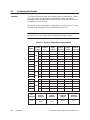
1
SIMATIC 505
Differential Analog Input Module
(PPX:505–2555)
User Manual
Order Number: PPX:505–8130–1
Manual Assembly Number: 2806134–0001
Original Edition
!
DANGER
DANGER indicates an imminently hazardous situation that, if not avoided, will
result in death or serious injury.
DANGER is limited to the most extreme situations.
!
WARNING
WARNING indicates a potentially hazardous situation that, if not avoided, could
result in death or serious injury, and/or property damage.
!
CAUTION
CAUTION indicates a potentially hazardous situation that, if not avoided, could
result in minor or moderate injury, and/or damage to property.
CAUTION is also used for property-damage-only accidents.
Copyright 1996 by Siemens Energy & Automation, Inc.
All Rights Reserved — Printed in USA
Reproduction, transmission, or use of this document or contents is not permitted without express consent of
Siemens Energy & Automation, Inc. All rights, including rights created by patent grant or registration of a utility model or design, are
reserved.
Since Siemens Energy & Automation, Inc., does not possess full access to data concerning all of the uses and applications of
customer’s products, we do not assume responsibility either for customer product design or for any infringements of patents or rights
of others which may result from our assistance.
MANUAL PUBLICATION HISTORY
SIMATIC 505 Differential Analog Input Module (PPX:505-2555) User Manual
Order Manual Number: PPX:505–8130–1
Refer to this history in all correspondence and/or discussion about this manual.
Event
Date
Description
Original Issue
04/96
Original Issue (2806134–0001)
LIST OF EFFECTIVE PAGES
Pages
Cover/Copyright
History/Effective Pages
iii — x
1-1 — 1-11
2-1 — 2-11
3-1 — 3-22
A-1 — A-3
B-1 — B-1
C-1 — C-1
D-1 — D-1
E-1 — E-2
F-1 — F-1
Registration
Description
Original
Original
Original
Original
Original
Original
Original
Original
Original
Original
Original
Original
Original
Pages
Description
Contents
Preface
Chapter 1
1.1
1.2
1.3
1.4
1.5
1.6
1.7
Description
Front Panel Description . . . . . . . . . . . . . . . . . . . . . . . . . . . . . . . . . . . . . . . . . . . . . . . . . . . . . . . . . .
1-2
Active LED . . . . . . . . . . . . . . . . . . . . . . . . . . . . . . . . . . . . . . . . . . . . . . . . . . . . . . . . . . . . . . . . . . . . .
Input Connector for Channels 1 – 16 . . . . . . . . . . . . . . . . . . . . . . . . . . . . . . . . . . . . . . . . . . . . .
1-2
1-2
Operating Modes . . . . . . . . . . . . . . . . . . . . . . . . . . . . . . . . . . . . . . . . . . . . . . . . . . . . . . . . . . . . . . .
1-3
Asynchronous Operation . . . . . . . . . . . . . . . . . . . . . . . . . . . . . . . . . . . . . . . . . . . . . . . . . . . . . . . .
Immediate I/O . . . . . . . . . . . . . . . . . . . . . . . . . . . . . . . . . . . . . . . . . . . . . . . . . . . . . . . . . . . . . . . . . .
Unipolar or Bipolar Mode . . . . . . . . . . . . . . . . . . . . . . . . . . . . . . . . . . . . . . . . . . . . . . . . . . . . . . . .
Voltage or Current Mode . . . . . . . . . . . . . . . . . . . . . . . . . . . . . . . . . . . . . . . . . . . . . . . . . . . . . . . .
1-3
1-3
1-3
1-3
Digital Word Map . . . . . . . . . . . . . . . . . . . . . . . . . . . . . . . . . . . . . . . . . . . . . . . . . . . . . . . . . . . . . . .
1-4
Overview . . . . . . . . . . . . . . . . . . . . . . . . . . . . . . . . . . . . . . . . . . . . . . . . . . . . . . . . . . . . . . . . . . . . . . .
Unipolar Presentation . . . . . . . . . . . . . . . . . . . . . . . . . . . . . . . . . . . . . . . . . . . . . . . . . . . . . . . . . . .
Bipolar Presentation . . . . . . . . . . . . . . . . . . . . . . . . . . . . . . . . . . . . . . . . . . . . . . . . . . . . . . . . . . . . .
1-4
1-4
1-4
Analog to Digital Conversion . . . . . . . . . . . . . . . . . . . . . . . . . . . . . . . . . . . . . . . . . . . . . . . . . . . .
1-5
Unipolar Mode Conversion . . . . . . . . . . . . . . . . . . . . . . . . . . . . . . . . . . . . . . . . . . . . . . . . . . . . . .
Bipolar Mode Conversion . . . . . . . . . . . . . . . . . . . . . . . . . . . . . . . . . . . . . . . . . . . . . . . . . . . . . . .
Example Conversion . . . . . . . . . . . . . . . . . . . . . . . . . . . . . . . . . . . . . . . . . . . . . . . . . . . . . . . . . . . .
1-5
1-5
1-5
Effect of Out-of-Range Input Signals . . . . . . . . . . . . . . . . . . . . . . . . . . . . . . . . . . . . . . . . . . . . .
1-6
Overview . . . . . . . . . . . . . . . . . . . . . . . . . . . . . . . . . . . . . . . . . . . . . . . . . . . . . . . . . . . . . . . . . . . . . . .
Unipolar Mode . . . . . . . . . . . . . . . . . . . . . . . . . . . . . . . . . . . . . . . . . . . . . . . . . . . . . . . . . . . . . . . . .
Bipolar Mode . . . . . . . . . . . . . . . . . . . . . . . . . . . . . . . . . . . . . . . . . . . . . . . . . . . . . . . . . . . . . . . . . . .
1-6
1-6
1-8
Using 20% Offset . . . . . . . . . . . . . . . . . . . . . . . . . . . . . . . . . . . . . . . . . . . . . . . . . . . . . . . . . . . . . . . .
1-10
Using the Module with 20% Offset . . . . . . . . . . . . . . . . . . . . . . . . . . . . . . . . . . . . . . . . . . . . . . . .
1-10
Resolution . . . . . . . . . . . . . . . . . . . . . . . . . . . . . . . . . . . . . . . . . . . . . . . . . . . . . . . . . . . . . . . . . . . . . .
1-11
Unipolar Mode Resolution . . . . . . . . . . . . . . . . . . . . . . . . . . . . . . . . . . . . . . . . . . . . . . . . . . . . . . .
Bipolar Mode Resolution . . . . . . . . . . . . . . . . . . . . . . . . . . . . . . . . . . . . . . . . . . . . . . . . . . . . . . . .
Input Resolution . . . . . . . . . . . . . . . . . . . . . . . . . . . . . . . . . . . . . . . . . . . . . . . . . . . . . . . . . . . . . . . .
1-11
1-11
1-11
Contents
iii
Chapter 2
2.1
2.2
2.3
2.4
2.5
Getting Started . . . . . . . . . . . . . . . . . . . . . . . . . . . . . . . . . . . . . . . . . . . . . . . . . . . . . . . . . . . . . . . . .
2-2
Overview of Installation Procedure . . . . . . . . . . . . . . . . . . . . . . . . . . . . . . . . . . . . . . . . . . . . . . .
2-2
Planning the Installation . . . . . . . . . . . . . . . . . . . . . . . . . . . . . . . . . . . . . . . . . . . . . . . . . . . . . . . . .
2-3
Overview . . . . . . . . . . . . . . . . . . . . . . . . . . . . . . . . . . . . . . . . . . . . . . . . . . . . . . . . . . . . . . . . . . . . . . .
Calculating the I/O Base Power Budget . . . . . . . . . . . . . . . . . . . . . . . . . . . . . . . . . . . . . . . . . .
Input Signal Wiring . . . . . . . . . . . . . . . . . . . . . . . . . . . . . . . . . . . . . . . . . . . . . . . . . . . . . . . . . . . . . .
Unpacking the Module . . . . . . . . . . . . . . . . . . . . . . . . . . . . . . . . . . . . . . . . . . . . . . . . . . . . . . . . . .
2-3
2-3
2-3
2-3
Configuring the Module . . . . . . . . . . . . . . . . . . . . . . . . . . . . . . . . . . . . . . . . . . . . . . . . . . . . . . . . .
2-4
Overview . . . . . . . . . . . . . . . . . . . . . . . . . . . . . . . . . . . . . . . . . . . . . . . . . . . . . . . . . . . . . . . . . . . . . . .
Changing the Configuration . . . . . . . . . . . . . . . . . . . . . . . . . . . . . . . . . . . . . . . . . . . . . . . . . . . .
Selecting Voltage or Current Input Mode (JP1, JP2, JP3, JP4) . . . . . . . . . . . . . . . . . . . . . .
Selecting Voltage Range (JP5–JP20) . . . . . . . . . . . . . . . . . . . . . . . . . . . . . . . . . . . . . . . . . . . . .
Selecting Unipolar or Bipolar Input Mode . . . . . . . . . . . . . . . . . . . . . . . . . . . . . . . . . . . . . . . . .
Selecting Digital Filtering . . . . . . . . . . . . . . . . . . . . . . . . . . . . . . . . . . . . . . . . . . . . . . . . . . . . . . . .
Digital Filter Time Constant . . . . . . . . . . . . . . . . . . . . . . . . . . . . . . . . . . . . . . . . . . . . . . . . . . . . . .
2-4
2-5
2-6
2-6
2-7
2-7
2-7
Installing the Module . . . . . . . . . . . . . . . . . . . . . . . . . . . . . . . . . . . . . . . . . . . . . . . . . . . . . . . . . . . .
2-8
Inserting the Module Into the I/O Base . . . . . . . . . . . . . . . . . . . . . . . . . . . . . . . . . . . . . . . . . . .
Wiring the Input Connectors . . . . . . . . . . . . . . . . . . . . . . . . . . . . . . . . . . . . . . . . . . . . . . . . . . . . .
Connecting Voltage Input Wiring . . . . . . . . . . . . . . . . . . . . . . . . . . . . . . . . . . . . . . . . . . . . . . . .
Connecting Current Input Wiring . . . . . . . . . . . . . . . . . . . . . . . . . . . . . . . . . . . . . . . . . . . . . . . .
Inserting the Screw Terminal Connector . . . . . . . . . . . . . . . . . . . . . . . . . . . . . . . . . . . . . . . . . .
2-8
2-8
2-9
2-9
2-10
Checking Module Operation . . . . . . . . . . . . . . . . . . . . . . . . . . . . . . . . . . . . . . . . . . . . . . . . . . . .
2-11
Checking Module Status . . . . . . . . . . . . . . . . . . . . . . . . . . . . . . . . . . . . . . . . . . . . . . . . . . . . . . . .
Checking Module Configuration in Controller Memory . . . . . . . . . . . . . . . . . . . . . . . . . . . .
2-11
2-11
Chapter 3
3.1
3.2
iv
Installation
Advanced Function Programming
Advanced Software Functions . . . . . . . . . . . . . . . . . . . . . . . . . . . . . . . . . . . . . . . . . . . . . . . . . . .
3-2
Introduction . . . . . . . . . . . . . . . . . . . . . . . . . . . . . . . . . . . . . . . . . . . . . . . . . . . . . . . . . . . . . . . . . . . .
Overview of the Advanced Functions . . . . . . . . . . . . . . . . . . . . . . . . . . . . . . . . . . . . . . . . . . . .
Setting the Module Configuration Jumper for Advanced Mode . . . . . . . . . . . . . . . . . . .
Logging the Module in the Controller I/O Configuration Memory . . . . . . . . . . . . . . . . . .
3-2
3-2
3-3
3-4
Internal Register Structures . . . . . . . . . . . . . . . . . . . . . . . . . . . . . . . . . . . . . . . . . . . . . . . . . . . . . .
3-5
Description of the I/O Registers . . . . . . . . . . . . . . . . . . . . . . . . . . . . . . . . . . . . . . . . . . . . . . . . . .
Input Registers . . . . . . . . . . . . . . . . . . . . . . . . . . . . . . . . . . . . . . . . . . . . . . . . . . . . . . . . . . . . . . . . . .
Output Registers . . . . . . . . . . . . . . . . . . . . . . . . . . . . . . . . . . . . . . . . . . . . . . . . . . . . . . . . . . . . . . . .
Control Registers . . . . . . . . . . . . . . . . . . . . . . . . . . . . . . . . . . . . . . . . . . . . . . . . . . . . . . . . . . . . . . . .
Inputs . . . . . . . . . . . . . . . . . . . . . . . . . . . . . . . . . . . . . . . . . . . . . . . . . . . . . . . . . . . . . . . . . . . . . . . . . .
Outputs . . . . . . . . . . . . . . . . . . . . . . . . . . . . . . . . . . . . . . . . . . . . . . . . . . . . . . . . . . . . . . . . . . . . . . . .
Loading Data into the PPX:505-2555 Module . . . . . . . . . . . . . . . . . . . . . . . . . . . . . . . . . . . . .
3-5
3-5
3-7
3-8
3-8
3-8
3-10
Contents
3.3
Loading Programs into the I/O Module . . . . . . . . . . . . . . . . . . . . . . . . . . . . . . . . . . . . . . . . . . .
3-14
3.4
Timing Considerations . . . . . . . . . . . . . . . . . . . . . . . . . . . . . . . . . . . . . . . . . . . . . . . . . . . . . . . . . . .
3-16
Timing Constraints When Using Advanced Functions . . . . . . . . . . . . . . . . . . . . . . . . . . . . . .
3-16
Additional Information about Each Function . . . . . . . . . . . . . . . . . . . . . . . . . . . . . . . . . . . . . .
3-17
Default Values . . . . . . . . . . . . . . . . . . . . . . . . . . . . . . . . . . . . . . . . . . . . . . . . . . . . . . . . . . . . . . . . . .
Offset Mode . . . . . . . . . . . . . . . . . . . . . . . . . . . . . . . . . . . . . . . . . . . . . . . . . . . . . . . . . . . . . . . . . . . .
Scaling . . . . . . . . . . . . . . . . . . . . . . . . . . . . . . . . . . . . . . . . . . . . . . . . . . . . . . . . . . . . . . . . . . . . . . . . .
Alarm Setpoints . . . . . . . . . . . . . . . . . . . . . . . . . . . . . . . . . . . . . . . . . . . . . . . . . . . . . . . . . . . . . . . . .
Digital Filtering . . . . . . . . . . . . . . . . . . . . . . . . . . . . . . . . . . . . . . . . . . . . . . . . . . . . . . . . . . . . . . . . . .
Averaging . . . . . . . . . . . . . . . . . . . . . . . . . . . . . . . . . . . . . . . . . . . . . . . . . . . . . . . . . . . . . . . . . . . . . .
Peak and Valley Hold . . . . . . . . . . . . . . . . . . . . . . . . . . . . . . . . . . . . . . . . . . . . . . . . . . . . . . . . . . .
Peak and Valley Hold Reset . . . . . . . . . . . . . . . . . . . . . . . . . . . . . . . . . . . . . . . . . . . . . . . . . . . . .
Flag Bits . . . . . . . . . . . . . . . . . . . . . . . . . . . . . . . . . . . . . . . . . . . . . . . . . . . . . . . . . . . . . . . . . . . . . . . .
Advanced Function Precedence . . . . . . . . . . . . . . . . . . . . . . . . . . . . . . . . . . . . . . . . . . . . . . . .
3-17
3-17
3-18
3-18
3-19
3-20
3-20
3-21
3-21
3-22
3.5
Appendix A
Troubleshooting
A.1
Troubleshooting the Module . . . . . . . . . . . . . . . . . . . . . . . . . . . . . . . . . . . . . . . . . . . . . . . . . . . . .
A-2
A.2
Troubleshooting the System . . . . . . . . . . . . . . . . . . . . . . . . . . . . . . . . . . . . . . . . . . . . . . . . . . . . . .
A-3
Appendix B
Specifications. . . . . . . . . . . . . . . . . . . . . . . . . . . . . . . . . . . . . . . . . .
Appendix C
Jumper Settings Log Sheet. . . . . . . . . . . . . . . . . . . . . . . . . . . . . . . C-1
Appendix D
I/O Register Quick Reference . . . . . . . . . . . . . . . . . . . . . . . . . . . . D-1
Appendix E
V- or K-Memory Configuration Table. . . . . . . . . . . . . . . . . . . . . . .
E-1
Appendix F
Addressing Worksheet . . . . . . . . . . . . . . . . . . . . . . . . . . . . . . . . . .
F-1
Contents
B-1
v
List of Figures
1-1
1-2
1-3
1-4
1-5
1-6
1-7
1-8
1-9
1-10
PPX:505-2555 Front Panel Description . . . . . . . . . . . . . . . . . . . . . . . . . . . . . . . . . . . . . . . . . . . .
Word Input to the PLC from the Module (Unipolar) . . . . . . . . . . . . . . . . . . . . . . . . . . . . . . . .
Word Input to the PLC from the Module (Bipolar) . . . . . . . . . . . . . . . . . . . . . . . . . . . . . . . . .
Example of Change in Input Level . . . . . . . . . . . . . . . . . . . . . . . . . . . . . . . . . . . . . . . . . . . . . . .
Voltage Input Limits (Unipolar) . . . . . . . . . . . . . . . . . . . . . . . . . . . . . . . . . . . . . . . . . . . . . . . . . . .
Typical Unipolar Overrange Word Value . . . . . . . . . . . . . . . . . . . . . . . . . . . . . . . . . . . . . . . . . .
Typical Unipolar Underrange Word Value . . . . . . . . . . . . . . . . . . . . . . . . . . . . . . . . . . . . . . . . .
Voltage Input Limits (Bipolar) . . . . . . . . . . . . . . . . . . . . . . . . . . . . . . . . . . . . . . . . . . . . . . . . . . . .
Typical Bipolar Overrange Word Value . . . . . . . . . . . . . . . . . . . . . . . . . . . . . . . . . . . . . . . . . . .
Typical Bipolar Underrange Word Value . . . . . . . . . . . . . . . . . . . . . . . . . . . . . . . . . . . . . . . . . .
1-2
1-4
1-4
1-5
1-6
1-7
1-7
1-8
1-9
1-9
2-1
2-2
2-3
2-4
2-5
2-6
Configuration Jumper Locations . . . . . . . . . . . . . . . . . . . . . . . . . . . . . . . . . . . . . . . . . . . . . . . . .
Screw Terminal Plug Wiring . . . . . . . . . . . . . . . . . . . . . . . . . . . . . . . . . . . . . . . . . . . . . . . . . . . . . .
Typical Internal Circuit — Voltage Mode . . . . . . . . . . . . . . . . . . . . . . . . . . . . . . . . . . . . . . . . .
Typical Internal Circuit — Current Mode . . . . . . . . . . . . . . . . . . . . . . . . . . . . . . . . . . . . . . . . . .
Input Connector Assembly . . . . . . . . . . . . . . . . . . . . . . . . . . . . . . . . . . . . . . . . . . . . . . . . . . . . . .
Example I/O Configuration Chart . . . . . . . . . . . . . . . . . . . . . . . . . . . . . . . . . . . . . . . . . . . . . . . .
2-7
2-8
2-9
2-9
2-10
2-11
3-1
3-2
3-3
3-4
3-5
3-6
3-7
3-8
3-9
3-10
3-11
3-12
3-13
3-14
3-15
3-16
Configuring the PPX:505-2555 for Advanced Functions . . . . . . . . . . . . . . . . . . . . . . . . . . .
PPX:505-2555 I/O Configuration Chart . . . . . . . . . . . . . . . . . . . . . . . . . . . . . . . . . . . . . . . . . . . .
Input Flag Bits . . . . . . . . . . . . . . . . . . . . . . . . . . . . . . . . . . . . . . . . . . . . . . . . . . . . . . . . . . . . . . . . . . .
Module_Ready Bit . . . . . . . . . . . . . . . . . . . . . . . . . . . . . . . . . . . . . . . . . . . . . . . . . . . . . . . . . . . . . .
Data Transfer Control Bits . . . . . . . . . . . . . . . . . . . . . . . . . . . . . . . . . . . . . . . . . . . . . . . . . . . . . . . .
Data Loading Process . . . . . . . . . . . . . . . . . . . . . . . . . . . . . . . . . . . . . . . . . . . . . . . . . . . . . . . . . . .
Sample Low and High Alarm Setpoints . . . . . . . . . . . . . . . . . . . . . . . . . . . . . . . . . . . . . . . . . . .
The Module_Ready Bit . . . . . . . . . . . . . . . . . . . . . . . . . . . . . . . . . . . . . . . . . . . . . . . . . . . . . . . . . .
Identifying the Data Being Transferred . . . . . . . . . . . . . . . . . . . . . . . . . . . . . . . . . . . . . . . . . . .
The Data_Ready Bit . . . . . . . . . . . . . . . . . . . . . . . . . . . . . . . . . . . . . . . . . . . . . . . . . . . . . . . . . . . . .
Enabling the Functions Loaded . . . . . . . . . . . . . . . . . . . . . . . . . . . . . . . . . . . . . . . . . . . . . . . . . .
Loading the Enable Bits . . . . . . . . . . . . . . . . . . . . . . . . . . . . . . . . . . . . . . . . . . . . . . . . . . . . . . . . .
505-2555 Configuration Example Program . . . . . . . . . . . . . . . . . . . . . . . . . . . . . . . . . . . . . . . .
Peak/Valley Truth Table . . . . . . . . . . . . . . . . . . . . . . . . . . . . . . . . . . . . . . . . . . . . . . . . . . . . . . . . . .
Peak/Valley Reset Truth Table . . . . . . . . . . . . . . . . . . . . . . . . . . . . . . . . . . . . . . . . . . . . . . . . . . . .
Mapping Bit Position to Channel Number . . . . . . . . . . . . . . . . . . . . . . . . . . . . . . . . . . . . . . . .
3-3
3-4
3-6
3-8
3-9
3-10
3-11
3-11
3-12
3-12
3-13
3-13
3-15
3-20
3-21
3-21
F-1
Addressing Worksheet . . . . . . . . . . . . . . . . . . . . . . . . . . . . . . . . . . . . . . . . . . . . . . . . . . . . . . . . . . .
F-1
vi
Contents
List of Tables
1-1
Input Resolution . . . . . . . . . . . . . . . . . . . . . . . . . . . . . . . . . . . . . . . . . . . . . . . . . . . . . . . . . . . . . . . .
1-11
2-1
Factory Configuration Jumper Settings . . . . . . . . . . . . . . . . . . . . . . . . . . . . . . . . . . . . . . . . . . .
2-4
3-1
3-2
3-3
3-4
3-5
3-6
3-7
3-8
Input and Output Register Offsets . . . . . . . . . . . . . . . . . . . . . . . . . . . . . . . . . . . . . . . . . . . . . . . .
Input Channel Data . . . . . . . . . . . . . . . . . . . . . . . . . . . . . . . . . . . . . . . . . . . . . . . . . . . . . . . . . . . . .
Peak/Valley Hold Input Words . . . . . . . . . . . . . . . . . . . . . . . . . . . . . . . . . . . . . . . . . . . . . . . . . . .
Output Data Registers . . . . . . . . . . . . . . . . . . . . . . . . . . . . . . . . . . . . . . . . . . . . . . . . . . . . . . . . . .
Function Enable Bits . . . . . . . . . . . . . . . . . . . . . . . . . . . . . . . . . . . . . . . . . . . . . . . . . . . . . . . . . . . . .
Data Identification Bits . . . . . . . . . . . . . . . . . . . . . . . . . . . . . . . . . . . . . . . . . . . . . . . . . . . . . . . . . .
Timing Overhead for Functions Enabled . . . . . . . . . . . . . . . . . . . . . . . . . . . . . . . . . . . . . . . . . .
Default Function Values . . . . . . . . . . . . . . . . . . . . . . . . . . . . . . . . . . . . . . . . . . . . . . . . . . . . . . . . .
3-5
3-5
3-6
3-7
3-8
3-9
3-16
3-17
A-1
A-2
Troubleshooting Matrix . . . . . . . . . . . . . . . . . . . . . . . . . . . . . . . . . . . . . . . . . . . . . . . . . . . . . . . . . .
Troubleshooting Flow Diagram . . . . . . . . . . . . . . . . . . . . . . . . . . . . . . . . . . . . . . . . . . . . . . . . . . .
A-2
A-3
B-1
Physical and Environmental Specifications . . . . . . . . . . . . . . . . . . . . . . . . . . . . . . . . . . . . . . .
B-1
C-1
Jumper Settings Log . . . . . . . . . . . . . . . . . . . . . . . . . . . . . . . . . . . . . . . . . . . . . . . . . . . . . . . . . . . .
C-1
Contents
vii
Preface
About This Manual
This user manual provides installation and operation instructions for the
PPX:505-2555 Sixteen Channel Differential Analog Input Module for
Series 505 programmable controllers. This manual assumes you are
familiar with the operation of Series 505 controllers (as described in the
manuals listed below, under “Related Manuals”).
Module
Compatibility
This module is compatible with all of the SIMATIC controllers except the
525. The 525 controller does not support the high-density WX16 mode
required for operation. Refer to the appropriate user documentation for
specific information on the Series 505 controllers and I/O modules.
Modes of
Operation
This module can operate in either of the following modes:
Organization
•
Standard mode: sixteen analog input channels, with several
configuration options. This mode is described in Chapters 1 and 2.
•
Advanced mode: high-density advanced functions, processed in the
module. This mode is described in Chapter 3.
This manual is organized as follows:
•
Chapter 1 provides a description of the module.
•
Chapter 2 covers configuration, installation, and wiring.
•
Chapter 3 covers advanced function programming.
•
Appendix A is a guide to troubleshooting.
•
Appendix B is a table of specifications.
•
Appendix C is a log sheet for your configuration jumper settings.
•
Appendix D is an I/O register quick reference chart.
•
Appendix E is a set of V-memory configuration tables.
•
Appendix F is an addressing worksheet.
Differential Analog Input Module User Manual
Preface
ix
Related Manuals
Additional manuals that have relevant information include the following:
•
SIMATIC 545/555/575 System Manual (PPX:505–8201–x).
•
SIMATIC 545/555/575 Programming Reference User Manual
(PPX:505–8204–x).
•
SIMATIC 505 TISOFT2 User Manual (PPX:TS505–8101–x).
Refer to material in these manuals as necessary for additional information
about programming and operating your 545/555/575 system.
Agency Standards
Series 505 products have been developed with consideration of the draft
standard of the International Electrotechnical Commission Committee
proposed standard (IEC–65A/WG6) for programmable controllers (released
as IEC 1131–2, Programmable Controllers, Part 2: Equipment
Requirements and Tests, First Edition, 1992–09). Contact Siemens Energy
& Automation, Inc., for information about regulatory agency approvals that
have been obtained on Series 505 units.
Agency Approvals
Agency approvals are the following:
– UL-listed (industrial control equipment)
– CUL (Canadian UL)
– FM (Class I, Div. 2, Group A, B, C, D Hazardous Locations)
European
Community (CE)
Approval
Generally, products listed in this manual comply with the essential
requirements of European Community EMC Directive, number 89/336/EEC,
and carry the CE label. See the declaration of conformity included with each
CPU for a listing of specific products and compliance details.
Technical
Assistance
For technical assistance, contact your Siemens Energy & Automation, Inc.,
distributor or sales office. If you need assistance in contacting your sales
agent or distributor in the United States, call 1–800–964–4114.
x
Preface
Differential Analog Input Module User Manual
Chapter 1
Description
1.1
1.2
1.3
1.4
1.5
1.6
1.7
Front Panel Description . . . . . . . . . . . . . . . . . . . . . . . . . . . . . . . . . . . . . . . . . . . . . . . . . . . . . . . . . .
1-2
Active LED . . . . . . . . . . . . . . . . . . . . . . . . . . . . . . . . . . . . . . . . . . . . . . . . . . . . . . . . . . . . . . . . . . . . .
Input Connector for Channels 1 – 16 . . . . . . . . . . . . . . . . . . . . . . . . . . . . . . . . . . . . . . . . . . . . .
1-2
1-2
Operating Modes . . . . . . . . . . . . . . . . . . . . . . . . . . . . . . . . . . . . . . . . . . . . . . . . . . . . . . . . . . . . . . .
1-3
Asynchronous Operation . . . . . . . . . . . . . . . . . . . . . . . . . . . . . . . . . . . . . . . . . . . . . . . . . . . . . . . .
Immediate I/O . . . . . . . . . . . . . . . . . . . . . . . . . . . . . . . . . . . . . . . . . . . . . . . . . . . . . . . . . . . . . . . . . .
Unipolar or Bipolar Mode . . . . . . . . . . . . . . . . . . . . . . . . . . . . . . . . . . . . . . . . . . . . . . . . . . . . . . . .
Voltage or Current Mode . . . . . . . . . . . . . . . . . . . . . . . . . . . . . . . . . . . . . . . . . . . . . . . . . . . . . . . .
1-3
1-3
1-3
1-3
Digital Word Map . . . . . . . . . . . . . . . . . . . . . . . . . . . . . . . . . . . . . . . . . . . . . . . . . . . . . . . . . . . . . . .
1-4
Overview . . . . . . . . . . . . . . . . . . . . . . . . . . . . . . . . . . . . . . . . . . . . . . . . . . . . . . . . . . . . . . . . . . . . . . .
Unipolar Presentation . . . . . . . . . . . . . . . . . . . . . . . . . . . . . . . . . . . . . . . . . . . . . . . . . . . . . . . . . . .
Bipolar Presentation . . . . . . . . . . . . . . . . . . . . . . . . . . . . . . . . . . . . . . . . . . . . . . . . . . . . . . . . . . . . .
1-4
1-4
1-4
Analog to Digital Conversion . . . . . . . . . . . . . . . . . . . . . . . . . . . . . . . . . . . . . . . . . . . . . . . . . . . .
1-5
Unipolar Mode Conversion . . . . . . . . . . . . . . . . . . . . . . . . . . . . . . . . . . . . . . . . . . . . . . . . . . . . . .
Bipolar Mode Conversion . . . . . . . . . . . . . . . . . . . . . . . . . . . . . . . . . . . . . . . . . . . . . . . . . . . . . . .
Example Conversion . . . . . . . . . . . . . . . . . . . . . . . . . . . . . . . . . . . . . . . . . . . . . . . . . . . . . . . . . . . .
1-5
1-5
1-5
Effect of Out-of-Range Input Signals . . . . . . . . . . . . . . . . . . . . . . . . . . . . . . . . . . . . . . . . . . . . .
1-6
Overview . . . . . . . . . . . . . . . . . . . . . . . . . . . . . . . . . . . . . . . . . . . . . . . . . . . . . . . . . . . . . . . . . . . . . . .
Unipolar Mode . . . . . . . . . . . . . . . . . . . . . . . . . . . . . . . . . . . . . . . . . . . . . . . . . . . . . . . . . . . . . . . . .
Bipolar Mode . . . . . . . . . . . . . . . . . . . . . . . . . . . . . . . . . . . . . . . . . . . . . . . . . . . . . . . . . . . . . . . . . . .
1-6
1-6
1-8
Using 20% Offset . . . . . . . . . . . . . . . . . . . . . . . . . . . . . . . . . . . . . . . . . . . . . . . . . . . . . . . . . . . . . . . .
1-10
Using the Module with 20% Offset . . . . . . . . . . . . . . . . . . . . . . . . . . . . . . . . . . . . . . . . . . . . . . . .
1-10
Resolution . . . . . . . . . . . . . . . . . . . . . . . . . . . . . . . . . . . . . . . . . . . . . . . . . . . . . . . . . . . . . . . . . . . . . .
1-11
Unipolar Mode Resolution . . . . . . . . . . . . . . . . . . . . . . . . . . . . . . . . . . . . . . . . . . . . . . . . . . . . . . .
Bipolar Mode Resolution . . . . . . . . . . . . . . . . . . . . . . . . . . . . . . . . . . . . . . . . . . . . . . . . . . . . . . . .
Input Resolution . . . . . . . . . . . . . . . . . . . . . . . . . . . . . . . . . . . . . . . . . . . . . . . . . . . . . . . . . . . . . . . .
1-11
1-11
1-11
Differential Analog Input Module User Manual
Description
1-1
1.1
Front Panel Description
The Sixteen Channel Analog Input Module (PPX:505-2555) is a member of
the Series 505 analog family of Input/Output (I/O) modules for Series 505
controllers. The PPX:505-2555 is designed to translate an analog input
signal into an equivalent digital word which is then sent to the controller.
Figure 1-1 shows the front panel of the Sixteen Channel Analog Input
Module.
Active LED
The active LED is illuminated when the module is functioning normally. If
the Active LED is not lit, refer to Appendix A for troubleshooting.
Input Connector for
Channels 1 – 16
This connector provides wiring terminals for channels 1–16.
ÂÂ
ÂÂ
ÂÂ
ÂÂ
ÂÂ
ÂÂ
ÂÂ
ÂÂ
ÂÂ
ÂÂ
ÂÂ
ÂÂ
ÂÂ
ÂÂ
ÂÂ
Active LED
Connector
505-2555
Figure 1-1 PPX:505-2555 Front Panel Description
1-2
Description
Differential Analog Input Module User Manual
1.2
Operating Modes
Asynchronous
Operation
The module operates asynchronously with respect to the controller (a scan
of the controller and input sampling of the module do not occur at the same
time). Instead, the module translates all analog inputs in one module
update (approximately 6 milliseconds) and stores the translated words in
buffer memory. The controller retrieves the stored words from the module
buffer memory at the start of the I/O scan.
Immediate I/O
The PPX:505-2555 Differential Analog Input Module is fully compatible
with the Immediate Input function in the 545 and 555 controllers.
Unipolar or Bipolar
Mode
The module may be configured to accept either unipolar or bipolar input
signals. Selection of unipolar or bipolar mode is made using one internal
jumper per channel (see Section 2.3).
Voltage or Current
Mode
Each of the module’s sixteen channels may be configured to receive either
voltage or current analog input signals. For unipolar input signals, the
range is 0 to 5 VDC, 0 to 10 VDC or 0 to +20 mA. For bipolar input signals,
the signal range is –5 to +5 VDC, –10 to +10 VDC or –20 to +20 mA.
Selection of voltage or current mode and voltage range are made via
internal jumpers (see Section 2.3).
Differential Analog Input Module User Manual
Description
1-3
1.3
Digital Word Map
Overview
A unipolar analog input signal is translated into a 14-bit digital word. A
bipolar input signal is translated into a 13-bit digital word plus 1-bit for the
polarity sign. Since the controller requires a 16-bit input word, the 14-bit
value from the converter is placed into a 16-bit word for transmittal to the
controller.
Unipolar
Presentation
As shown in Figure 1-2, of the two bits not used for the digital word, one is
used to show the sign of the word, one is used to note values which are
“overrange/underrange.”
Bit #
1
2
3
4
5
MSB
Sign: 1 = –
0=+
6
7
.
.
.
32 16 8
4
2
1
8
9 10 11 12 13 14 15 16
LSB
If overrange or
underrange, set to 1
Translated Digital Word
Unipolar Word Map
Figure 1-2 Word Input to the PLC from the Module (Unipolar)
Bipolar
Presentation
As shown in Figure 1-3, of the three bits not used for the digital word, one is
used to show the sign of the word, one is used to note values which are
“overrange,” and the remaining bit is not used and set to zero.
Bit #
1
MSB
Sign: 1 = –
0=+
2
3
4
5
6
7
.
.
.
32 16 8
8
9 10 11 12 13 14 15 16
Translated Digital Word
Bipolar Word Map
4
2
1
LSB
If overrange or
underrange, set to 1
Unused: set to 0
Figure 1-3 Word Input to the PLC from the Module (Bipolar)
NOTE: In the bipolar map, bit 15 is unused. There will, however, be cases
where bit 15 will not be zero as indicated. Bipolar mode consists of 13 bits
plus a sign bit. When this data is transformed to a 16-bit word space to the
controller, some codes will result that will include bit 15.
1-4
Description
Differential Analog Input Module User Manual
1.4
Analog to Digital Conversion
Unipolar Mode
Conversion
Bipolar Mode
Conversion
The following equations may be used to calculate the digital word which will
result from a particular voltage or current input in the unipolar input mode:
0 to 5 V Input Range Mode, Digital Word (WX) =
+Input voltage (V) x 32000
––––––––––––––––––––––
5 volts
0 to 10 V Input Range Mode, Digital Word (WX) =
+Input voltage (V) x 32000
––––––––––––––––––––––
10 volts
0 to 20 mA Input Range Mode, Digital Word (WX) =
+Input current (mA) x 32000
––––––––––––––––––––––––
20 mA
The following equations may be used to calculate the digital word which will
result from a particular voltage or current input in the bipolar input mode:
–5 to 5 V Input Range Mode, Digital Word (WX) =
± Input voltage (V) x 32000
––––––––––––––––––––––
5 volts
–10 to 10 V Input Range Mode, Digital Word (WX) =
± Input voltage (V) x 32000
––––––––––––––––––––––
10 volts
± Input current (mA) x 32000
–20 to 20 mA Input Range Mode, Digital Word (WX) = ––––––––––––––––––––––––
20 mA
Example
Conversion
Figure 1-4 illustrates the effects of a change in input level going from 0.3125
to 0.625 mV in the 0 to 5 V unipolar input mode. (For the 0 to 10 V and 0 to
20 mA unipolar input modes, or the bipolar modes, refer to the formulas
above to determine the digital word which results from a particular input.)
0.3125 mV x 32000 = 2
5V
0
0
0
0
0
0
0
.
.
.
32 16 8
4
2
1
0
0
0
0
0
0
1
0
.
.
.
32 16 8
4
2
1
0
0
0
0
0
1
0
0
.
.
.
32 16 8
4
2
1
1
0
0
0
0
0
0
0
MSB Sign: 1 = – , 0 = +
0.625 mV x 32000 = 4
5V
0
0
0
0
0
0
LSB
0
0
MSB
LSB
16,384
1.0 V x 32000 = 6400
5V
0
0
0
1
1
0
0
0
0
MSB
LSB
Figure 1-4 Example of Change in Input Level
Differential Analog Input Module User Manual
Description
1-5
1.5
Effect of Out-of-Range Input Signals
Overview
The PPX:505-2555 Differential Analog Input Module utilizes the overrange
and underrange bit to indicate when a channel has reached individual
limits. The value of the overrange or underrange condition varies from
channel to channel. The reason for this is that as a channel is calibrated, all
of the gains and offsets and dynamic ranges of the analog-to-digital
converter of the system are compensated for in each analog input channel.
Therefore, the point at which the analog-to-digital converter reaches a
saturation point and can no longer produce a change in counts for a
corresponding change in input signal is called the overrange or underrange
limit of the channel. This level is different for every channel.
In the figures below, the limits for the overrange and underrange values are
the minimum limits for a given channel. The actual limits for an individual
channel may be greater.
Unipolar Mode
Figure 1-5 shows the voltage input limits for unipolar mode. Signals falling
above or below the upper and lower limits in 0 to 5 V input mode or 0 to
10 V input mode are translated into a digital word that includes the
addition of bit 16 to indicate an overrange or underrange condition. Note
that although the digital word may approach zero as the analog input signal
approaches the minimum for a given range, the digital word will never
actually be zero. In fact, the underrange capability of any channel in
unipolar mode may produce a negative value to the controller for a number
of counts before the underrange bit is set.
Voltage range
0 to 5 V:
0 to 10 V:
–200 V
Module not
protected,
damage
might occur
–0.05 V
+5.05 V
–0.10 V
+10.10 V
Underrange
output data
Accuracy
within
specification
0
+200 V
Overrange
bit set
Module not
protected,
damage
might occur
32,320
Note: Limits will not be less than those listed, but can be greater.
Unipolar Mode
Figure 1-5 Voltage Input Limits (Unipolar)
1-6
Description
Differential Analog Input Module User Manual
Figure 1-6 and Figure 1-7 show the binary values of typical overrange and
underrange conditions for unipolar mode.
Typical Digital Word Map for Overrange Digital Word
16,384
Bit #1 0
1
Translated
value = +32309
64 32 16 8
1
1
1
MSB
Sign: 1 = –
0=+
1
1
0
0
0
1
1
0
1
0
1 Bit #16
LSB
If overrange,
set to 1
Translated Digital Word
Unipolar Mode
Figure 1-6 Typical Unipolar Overrange Word Value
Typical Digital Word Map for Underrange Digital Word
16,384
Bit #1 1
1
MSB
Sign: 1 = –
0=+
Translated
value = –403
64 32 16 8
1
1
1
1
1
0
0
1
1
Translated Digital Word
0
1
1
0
1 Bit #16
LSB
If underrange,
set to 1
Unipolar Mode
Figure 1-7 Typical Unipolar Underrange Word Value
Differential Analog Input Module User Manual
Description
1-7
Effect of Out-of-Range Input Signals (continued)
Bipolar Mode
Figure 1-8 shows the voltage input limits for bipolar mode. In bipolar mode,
signals above or below the upper and lower limits in the –5 to +5 VDC or
–10 to +10 VDC range are translated to a digital word and also utilize the
overrange or underrange bit. The actual limit for each channel will vary
from channel to channel as described above.
Voltage range
–5 to +5 V:
–10 to +10 V:
–200 V
Module not
protected,
damage
might occur
–5.05 V
0V
+5.05 V
–10.10 V
0V
+10.10 V
Underrange
output data
Accuracy
within
specification
–32,320
+200 V
Overrange
bit set
Module not
protected,
damage
might occur
32,320
Note: Limits will not be less than those listed, but can be greater.
Bipolar Mode
Figure 1-8 Voltage Input Limits (Bipolar)
1-8
Description
Differential Analog Input Module User Manual
Figure 1-9 and Figure 1-10 show the binary values of typical overrange and
underrange conditions for bipolar mode.
Typical Digital Word Map for Overrange Digital Word
16,384
Bit #1 0
1
Translated
value = +32687
64 32 16 8
1
1
1
MSB
Sign: 1 = –
0=+
1
1
1
1
0
1
0
1
1
1
1 Bit #16
LSB
If overrange,
set to 1
Translated Digital Word
Bipolar Mode
Figure 1-9 Typical Bipolar Overrange Word Value
Typical Digital Word Map for Underrange Digital Word
16,384
Bit #1 1
0
MSB
Sign: 1 = –
0=+
Translated
value = –32767
64 32 16 8
0
0
0
0
0
0
0
0
0
Translated Digital Word
0
0
0
0
1 Bit #16
LSB
If underrange,
set to 1
Bipolar Mode
Figure 1-10 Typical Bipolar Underrange Word Value
Differential Analog Input Module User Manual
Description
1-9
1.6
Using 20% Offset
Using the Module
with 20% Offset
Most applications use transducers that provide 1 to 5 volt (4 to 20 mA) input
signals instead of 0 to 5 volt (0 to 20 mA) input signals. You can allow for
this 20% offset by including some additional instructions in your RLL
(Relay Ladder Logic) program.
First, subtract 6400 from the input data word (WX). Then, multiply the
result by 125 and divide the product by 100. This yields the following
equation:
(WX–6400) x 125
––––––––––––––
100
= 20% offset data word
Consult your SIMATIC 545/555/575 Programming Reference User Manual
for information about the RLL instructions used in the conversion.
1-10
Description
Differential Analog Input Module User Manual
1.7
Resolution
Unipolar Mode
Resolution
In unipolar input mode, the module has a resolution of 2 counts out of
32000. That is, the smallest unit into which the module will divide an input
is 1 part out of 16000. This relationship can be shown as:
2 counts per step
––––––––––––––––––
32000 counts full scale
Bipolar Mode
Resolution
1
= ––––
16000
In bipolar mode, the resolution is 4 counts out of 32000, so that the smallest
unit into which the module will divide an input is 1 part out of 8000. This
relationship can be shown as:
4 counts per step
––––––––––––––––––
32000 counts full scale
1
= ––––
8000
When using the module with 20% offset, module resolution remains at 2
counts out of 32000, but offset resolution becomes 4 counts out of 32000 as a
result of the multiplication and division of the incoming data word.
Input Resolution
Table 1-1 shows the corresponding input resolution per step for each of the
input configuration modes:
Table 1-1 Input Resolution
Unipolar
Unipolar with
20% Offset
Bipolar
Differential Analog Input Module User Manual
Range
Configuration
Digital
Counts/Step
Input Resolution
Per Step
0 – 5 VDC
2
0.3125 mV
0 – 10 VDC
2
0.625 mV
0 – 20 mA
2
1.25 A
1 – 5 VDC
4
0.625 mV
4 – 20 mA
4
2.50 A
–5 – +5 VDC
4
0.625 mV
–10 – +10 VDC
4
1.25 mV
–20 – +20 mA
4
2.50 A
Description
1-11
Chapter 2
Installation
2.1
2.2
2.3
2.4
2.5
Getting Started . . . . . . . . . . . . . . . . . . . . . . . . . . . . . . . . . . . . . . . . . . . . . . . . . . . . . . . . . . . . . . . . .
2-2
Overview of Installation Procedure . . . . . . . . . . . . . . . . . . . . . . . . . . . . . . . . . . . . . . . . . . . . . . .
2-2
Planning the Installation . . . . . . . . . . . . . . . . . . . . . . . . . . . . . . . . . . . . . . . . . . . . . . . . . . . . . . . . .
2-3
Overview . . . . . . . . . . . . . . . . . . . . . . . . . . . . . . . . . . . . . . . . . . . . . . . . . . . . . . . . . . . . . . . . . . . . . . .
Calculating the I/O Base Power Budget . . . . . . . . . . . . . . . . . . . . . . . . . . . . . . . . . . . . . . . . . .
Input Signal Wiring . . . . . . . . . . . . . . . . . . . . . . . . . . . . . . . . . . . . . . . . . . . . . . . . . . . . . . . . . . . . . .
Unpacking the Module . . . . . . . . . . . . . . . . . . . . . . . . . . . . . . . . . . . . . . . . . . . . . . . . . . . . . . . . . .
2-3
2-3
2-3
2-3
Configuring the Module . . . . . . . . . . . . . . . . . . . . . . . . . . . . . . . . . . . . . . . . . . . . . . . . . . . . . . . . .
2-4
Overview . . . . . . . . . . . . . . . . . . . . . . . . . . . . . . . . . . . . . . . . . . . . . . . . . . . . . . . . . . . . . . . . . . . . . . .
Changing the Configuration . . . . . . . . . . . . . . . . . . . . . . . . . . . . . . . . . . . . . . . . . . . . . . . . . . . .
Selecting Voltage or Current Input Mode (JP1, JP2, JP3, JP4) . . . . . . . . . . . . . . . . . . . . . .
Selecting Voltage Range (JP5–JP20) . . . . . . . . . . . . . . . . . . . . . . . . . . . . . . . . . . . . . . . . . . . . .
Selecting Unipolar or Bipolar Input Mode . . . . . . . . . . . . . . . . . . . . . . . . . . . . . . . . . . . . . . . . .
Selecting Digital Filtering . . . . . . . . . . . . . . . . . . . . . . . . . . . . . . . . . . . . . . . . . . . . . . . . . . . . . . . .
Digital Filter Time Constant . . . . . . . . . . . . . . . . . . . . . . . . . . . . . . . . . . . . . . . . . . . . . . . . . . . . . .
2-4
2-5
2-6
2-6
2-7
2-7
2-7
Installing the Module . . . . . . . . . . . . . . . . . . . . . . . . . . . . . . . . . . . . . . . . . . . . . . . . . . . . . . . . . . . .
2-8
Inserting the Module Into the I/O Base . . . . . . . . . . . . . . . . . . . . . . . . . . . . . . . . . . . . . . . . . . .
Wiring the Input Connectors . . . . . . . . . . . . . . . . . . . . . . . . . . . . . . . . . . . . . . . . . . . . . . . . . . . . .
Connecting Voltage Input Wiring . . . . . . . . . . . . . . . . . . . . . . . . . . . . . . . . . . . . . . . . . . . . . . . .
Connecting Current Input Wiring . . . . . . . . . . . . . . . . . . . . . . . . . . . . . . . . . . . . . . . . . . . . . . . .
Inserting the Screw Terminal Connector . . . . . . . . . . . . . . . . . . . . . . . . . . . . . . . . . . . . . . . . . .
2-8
2-8
2-9
2-9
2-10
Checking Module Operation . . . . . . . . . . . . . . . . . . . . . . . . . . . . . . . . . . . . . . . . . . . . . . . . . . . .
2-11
Checking Module Status . . . . . . . . . . . . . . . . . . . . . . . . . . . . . . . . . . . . . . . . . . . . . . . . . . . . . . . .
Checking Module Configuration in Controller Memory . . . . . . . . . . . . . . . . . . . . . . . . . . . .
2-11
2-11
Differential Analog Input Module User Manual
Installation
2-1
2.1
Getting Started
Overview of
Installation
Procedure
The installation of the Sixteen Channel Analog Input Module involves the
following steps:
Planning the installation
Configuring the module
Inserting the module into the I/O base
Wiring and connecting the module input connectors
Checking module operation
The steps listed above are explained in detail in the following pages.
2-2
Installation
Differential Analog Input Module User Manual
2.2
Planning the Installation
Overview
Planning is the first step in the installation of the module. This involves
calculating the I/O base power budget and routing the input signal wiring to
minimize noise. The following sections discuss these important
considerations.
Calculating the I/O
Base Power Budget
The PPX:505-2555 requires 5.0 watts of +5 VDC power from the I/O base.
Use this value to verify that the base power supply capacity is not exceeded.
Input Signal Wiring
Input signal wiring must be shielded twisted-pair cable. The shielding for
the cable should always be terminated at the module. Each group of four
input channels contains two termination points for the shield wire. Since
the cable shielding is grounded at the module, it should not be connected at
the opposite end.
The shield wire should be terminated only at the designated shield
terminals to minimize the effects of noise on the measuring system.
Note the following general considerations when wiring the module:
Unpacking the
Module
•
Always use the shortest possible cables
•
Avoid placing low voltage wire parallel to high energy wire (if the two
wires must meet, cross them at a right angle)
•
Avoid bending the wire into sharp angles
•
Use wireways for wire routing
•
Avoid placing wires on any vibrating surface
Open the shipping carton and remove the special anti-static bag which
contains the module.
!
CAUTION
The components on the PPX:505-2555 module printed circuit card can be
damaged by static electricity discharge. To prevent this damage, the module is
shipped in a special anti-static bag.
Static control precautions should be followed when removing the module from
the bag, when opening the module, and when handling the printed circuit card
during configuration.
After discharging any static build-up, remove the module from the static
bag. Do not discard the static bag. Always use this bag for protection
against static damage when the module is not inserted into the I/O
backplane.
Differential Analog Input Module User Manual
Installation
2-3
2.3
Configuring the Module
Overview
The Sixteen Channel Analog Input Module must be configured for voltage
or current inputs, voltage range, unipolar/bipolar mode, and digital
filtering/no filtering mode before wiring the input connector and inserting
the module into the I/O base.
As shipped, all input channels are configured for current inputs, 5 V range,
unipolar mode, and digital filtering enabled (see Table 2-1).
NOTE: The 5 V input signal range configuration is used for both 0 to 5 VDC
and 1 to 5 VDC or 4 to 20 mA and 0 to 20 mA input signal ranges.
Table 2-1 Factory Configuration Jumper Settings
Voltage/
Current
Jumper
Jumper
Position
V or I
Voltage
Range
Jumper
Jumper
Position
5 V or 10 V
Unipolar/
Bipolar
Jumper
UNI or BIP
1
I
JP5
5V
JP5
UNI
2
I
JP6
5V
JP6
UNI
3
I
JP7
5V
JP7
UNI
4
4
I
JP8
5V
JP8
UNI
5
5
I
JP9
5V
JP9
UNI
6
I
JP10
5V
JP10
UNI
7
I
JP11
5V
JP11
UNI
8
8
I
JP12
5V
JP12
UNI
9
9
I
JP13
5V
JP13
UNI
10
I
JP14
5V
JP14
UNI
11
I
JP15
5V
JP15
UNI
12
12
I
JP16
5V
JP16
UNI
13
13
I
JP17
5V
JP17
UNI
14
I
JP18
5V
JP18
UNI
15
I
JP19
5V
JP19
UNI
16
I
JP20
5V
JP20
UNI
Channel
Number
1
2
3
JP1
6
7
JP2
10
11
JP3
14
15
JP4
16
All
Channels
1–16
2-4
Installation
Unipolar/
Bipolar
Switches
Voltage
Range
Switches
SW7
SW5
SW8
SW6
Jumper
Position
Digital
Filtering
Jumper
Jumper
Position
FIL/none
JP121
FIL
Differential Analog Input Module User Manual
Changing the
Configuration
Changing the module input channel configuration involves the following
steps:
Selecting voltage (V) or current (I) input mode for each channel
Selecting 0 to 5 V or 0 to 10 V voltage range for each channel
Selecting unipolar or bipolar input mode for each channel
Selecting digital filtering or no filtering for the module
Logging the configuration jumper settings for future reference
Each of these steps is described in the following sections.
Differential Analog Input Module User Manual
Installation
2-5
Configuring the Module (continued)
Selecting Voltage
or Current Input
Mode (JP1, JP2,
JP3, JP4)
Locate the 16 Voltage/Current Jumpers corresponding to input channels 1
through 16. See Figure 2-1 for the location of these jumpers. For each input
channel, select current mode by placing the jumper in the “Current” position
or voltage mode by placing the jumper in the “Voltage” position. For each
input channel set to current mode, you must set the corresponding Voltage
Range Jumper to the 5 V position as described in the following section.
The silkscreen on the printed circuit board is clearly marked to indicate the
voltage or current position for each channel.
NOTE: Each channel utilizes jumpers to configure the hardware and DIP
switches to configure the microcomputer.
Selecting Voltage
Range (JP5–JP20)
Locate the Voltage Range Jumpers corresponding to input channels 1
through 16 (see Figure 2-1). For each input channel operating in current
mode, set the corresponding Voltage Range Jumper to 5 V.
!
CAUTION
Failure to properly configure each input channel for current mode could result
in damage to equipment.
Ensure you set the corresponding Voltage Range Jumper to 5 V.
For each input channel operating in voltage mode, set the corresponding
Voltage Range Jumper to 5 V for 0 to +5 VDC input range or 10 V for 0 to
10 VDC or –10 to +10 VDC input range. Locate DIP switches SW5 and SW6
and for each channel select the voltage range as previously selected with the
jumpers.
2-6
Installation
Differential Analog Input Module User Manual
Selecting Unipolar
or Bipolar Input
Mode
Locate the Unipolar/Bipolar Jumpers JP5 through JP20 (see Figure 2-1).
For each channel select UNI or BIP for Unipolar or Bipolar mode. Next set
DIP switches SW7 and SW8 for each channel to the same selection as the
corresponding jumpers JP5–JP20.
Selecting Digital
Filtering
Locate the Digital Filtering/No Filtering Jumper JP121 (see Figure 2-1). To
enable digital filtering, set the jumper in the FIL position. Since many
analog input signals contain noise, use digital filtering unless maximum
response time is required.
Digital Filter Time
Constant
The time constant for the module is 25 milliseconds. An input signal from
zero to full scale will require 4 to 5 time constants to reach a final value.
Therefore the effect of digital filtering will slow the response of the module
to 100 milliseconds.
JP4
JP20
JP3
JP18
JP19
JP16
JP17
JP2
JP14
JP12
JP15 JP13
SW8
SW7
SW6
SW5
JP1
JP10
JP11
JP8
JP9
JP6
JP7
JP5
JP121
DIGITAL
FILTERING
ENABLED
F1
Figure 2-1 Configuration Jumper Locations
Differential Analog Input Module User Manual
Installation
2-7
2.4
Installing the Module
Inserting the
Module Into the
I/O Base
Insert the module into the I/O base by carefully pushing the module into the
slot. When the module is fully seated in the slot and backplane connector,
tighten the captive screws at the top and bottom to hold the module in
place. To remove the module from the I/O base, loosen the captive screws,
then remove the module from the I/O base. Be careful not to damage the
DIN connector at the back of the module when inserting or removing the
module.
!
WARNING
Failure to remove power before inserting the module into the I/O rack could
result in damage to equipment and/or injury to personnel.
Remove all power to the I/O rack before inserting module.
Wiring the Input
Connectors
Input signals are accepted through a connector assembly located on the
front of the module. The connector assembly consists of a standard
Series 505 wiring connector (see Figure 2-5). Wiring is connected through
the screw terminal plug. The screw terminals can accept wire sizes up to
single-stranded 14 gauge wire. The actual size wire used depends on the
external device providing the input signal. Consult the device
manufacturer’s recommendations for selecting the input wire size.
To assign an input to a specific channel, locate the appropriate channel
position on the screw terminal plug as shown in Figure 2-2.
Figure 2-2 Screw Terminal Plug Wiring
2-8
Installation
Differential Analog Input Module User Manual
Connecting
Voltage Input
Wiring
For voltage input circuits, connect the signal wire to the + (positive) screw
terminal, and the return wire to the – (negative) screw terminal.
The ground terminals labeled SHIELD provide a convenient location to
terminate the shield. Insert the wires in the appropriate holes on the front
of the connector adjacent to the corresponding screw. When the wires are
inserted, tighten the screws. Repeat this procedure for the remaining
voltage input channels. The inputs of this module are full differential input
amplifiers that may be driven in a differential or single-ended mode. See
Figure 2-3.
+V
+
–
–V
SHIELD
Figure 2-3 Typical Internal Circuit — Voltage Mode
Connecting
Current Input
Wiring
For current input circuits, connect the signal wire to the + (positive) screw
terminal, and the return wire to the – (negative) screw terminal.
The ground terminals labeled SHIELD provide a convenient location to
terminate the shield. Insert the wires in the appropriate holes on the front
of the connector adjacent to the corresponding screw. When the wires are
inserted, tighten the screws. Repeat this procedure for the remaining
current input channels. See Figure 2-4.
+V
+
250
OHM
–
–V
SHIELD
Figure 2-4 Typical Internal Circuit — Current Mode
NOTE: No external current resistor is required in current mode.
Differential Analog Input Module User Manual
Installation
2-9
Installing the Module (continued)
Inserting the Screw
Terminal
Connector
When all the input signal wires are connected to the screw terminal, align
the edge of the printed circuit board with the corresponding edge of the
wiring connector, and press the connector on the circuit board until the
connector is fully seated. Next, align the captive screws on the top and
bottom of the connector with the front panel and tighten until the module
connector is fully seated. See Figure 2-5.
Printed Circuit Board (PCB)
Captive Screws
Individual Captive Screw
Input Signal Wires
Front Face Connector
Figure 2-5 Input Connector Assembly
2-10
Installation
Differential Analog Input Module User Manual
2.5
Checking Module Operation
Checking Module
Status
First turn on the base power supply. If the module diagnostics detect no
problems, the status indicator on the front of the module will light. If the
status indicator does not light, blinks, or goes out during operation, the
module has detected a failure. For information on viewing failed module
status, refer to your SIMATIC TISOFT User Manual. To diagnose and
correct a module failure, refer to the next section on troubleshooting.
Checking Module
Configuration in
Controller Memory
You must also check that the module is configured in the memory of the
controller. This is important because the module will appear to be
functioning regardless of whether it is communicating with the controller.
To view the controller memory configuration chart listing all slots on the
base and the inputs or outputs associated with each slot, refer to your
SIMATIC TISOFT Programming Manual. An example chart is shown in
Figure 2-6. The PPX:505-2555 logs in to the controller as 16 WX inputs.
505 I/O MODULE DEFINITION FOR CHANNEL . 1
SLOT
01
02
.
.
.
15
16
I/O
ADDRESS
BASE . . . 00
NUMBER OF BIT AND WORD I/O
X
Y
WX
WY
SPECIAL
FUNCTION
. . . . . 0001 . . . . . . 00 . . . . 00 . . . . 16 . . . 00 . . . . . . . NO
. . . . . 0000 . . . . . . 00 . . . . 00 . . . . 00 . . . 00 . . . . . . . NO
. . . . . 0000 . . . . . . 00 . . . . 00 . . . . 00 . . . 00 . . . . . . . NO
. . . . . 0000 . . . . . . 00 . . . . 00 . . . . 00 . . . 00 . . . . . . . NO
Figure 2-6 Example I/O Configuration Chart
In this example, the PPX:505-2555 module is inserted in slot 1 in I/O base 0.
Data for channel 1 appears in word location WX1, data for channel 2
appears in word location WX2, etc. For your particular module, look in the
chart for the number corresponding to the slot occupied by the module. If
word memory locations appear on this line, then the module is registered in
the controller memory and the module is ready for operation.
If the line is blank or erroneous, re-check the module to ensure that it is
firmly seated in the slots. Generate the controller memory configuration
chart again. If the line is still incorrect, contact the Siemens Energy &
Automation, Inc., Technical Services Group in the U.S.A. at 423–461–2522.
In other countries, you can also contact the nearest Siemens distributor.
Differential Analog Input Module User Manual
Installation
2-11
Chapter 3
Advanced Function Programming
3.1
Advanced Software Functions . . . . . . . . . . . . . . . . . . . . . . . . . . . . . . . . . . . . . . . . . . . . . . . . . . .
3-2
Introduction . . . . . . . . . . . . . . . . . . . . . . . . . . . . . . . . . . . . . . . . . . . . . . . . . . . . . . . . . . . . . . . . . . . .
Overview of the Advanced Functions . . . . . . . . . . . . . . . . . . . . . . . . . . . . . . . . . . . . . . . . . . . .
Setting the Module Configuration Jumper for Advanced Mode . . . . . . . . . . . . . . . . . . .
Logging the Module in the Controller I/O Configuration Memory . . . . . . . . . . . . . . . . . .
3-2
3-2
3-3
3-4
Internal Register Structures . . . . . . . . . . . . . . . . . . . . . . . . . . . . . . . . . . . . . . . . . . . . . . . . . . . . . .
3-5
Description of the I/O Registers . . . . . . . . . . . . . . . . . . . . . . . . . . . . . . . . . . . . . . . . . . . . . . . . . .
Input Registers . . . . . . . . . . . . . . . . . . . . . . . . . . . . . . . . . . . . . . . . . . . . . . . . . . . . . . . . . . . . . . . . . .
Output Registers . . . . . . . . . . . . . . . . . . . . . . . . . . . . . . . . . . . . . . . . . . . . . . . . . . . . . . . . . . . . . . . .
Control Registers . . . . . . . . . . . . . . . . . . . . . . . . . . . . . . . . . . . . . . . . . . . . . . . . . . . . . . . . . . . . . . . .
Inputs . . . . . . . . . . . . . . . . . . . . . . . . . . . . . . . . . . . . . . . . . . . . . . . . . . . . . . . . . . . . . . . . . . . . . . . . . .
Outputs . . . . . . . . . . . . . . . . . . . . . . . . . . . . . . . . . . . . . . . . . . . . . . . . . . . . . . . . . . . . . . . . . . . . . . . .
Loading Data into the PPX:505-2555 Module . . . . . . . . . . . . . . . . . . . . . . . . . . . . . . . . . . . . .
3-5
3-5
3-7
3-8
3-8
3-8
3-10
3.3
Loading Programs into the I/O Module . . . . . . . . . . . . . . . . . . . . . . . . . . . . . . . . . . . . . . . . . . .
3-14
3.4
Timing Considerations . . . . . . . . . . . . . . . . . . . . . . . . . . . . . . . . . . . . . . . . . . . . . . . . . . . . . . . . . . .
3-16
Timing Constraints When Using Advanced Functions . . . . . . . . . . . . . . . . . . . . . . . . . . . . . .
3-16
Additional Information about Each Function . . . . . . . . . . . . . . . . . . . . . . . . . . . . . . . . . . . . . .
3-17
Default Values . . . . . . . . . . . . . . . . . . . . . . . . . . . . . . . . . . . . . . . . . . . . . . . . . . . . . . . . . . . . . . . . . .
Offset Mode . . . . . . . . . . . . . . . . . . . . . . . . . . . . . . . . . . . . . . . . . . . . . . . . . . . . . . . . . . . . . . . . . . . .
Scaling . . . . . . . . . . . . . . . . . . . . . . . . . . . . . . . . . . . . . . . . . . . . . . . . . . . . . . . . . . . . . . . . . . . . . . . . .
Alarm Setpoints . . . . . . . . . . . . . . . . . . . . . . . . . . . . . . . . . . . . . . . . . . . . . . . . . . . . . . . . . . . . . . . . .
Digital Filtering . . . . . . . . . . . . . . . . . . . . . . . . . . . . . . . . . . . . . . . . . . . . . . . . . . . . . . . . . . . . . . . . . .
Averaging . . . . . . . . . . . . . . . . . . . . . . . . . . . . . . . . . . . . . . . . . . . . . . . . . . . . . . . . . . . . . . . . . . . . . .
Peak and Valley Hold . . . . . . . . . . . . . . . . . . . . . . . . . . . . . . . . . . . . . . . . . . . . . . . . . . . . . . . . . . .
Peak and Valley Hold Reset . . . . . . . . . . . . . . . . . . . . . . . . . . . . . . . . . . . . . . . . . . . . . . . . . . . . .
Flag Bits . . . . . . . . . . . . . . . . . . . . . . . . . . . . . . . . . . . . . . . . . . . . . . . . . . . . . . . . . . . . . . . . . . . . . . . .
Advanced Function Precedence . . . . . . . . . . . . . . . . . . . . . . . . . . . . . . . . . . . . . . . . . . . . . . . .
3-17
3-17
3-18
3-18
3-19
3-20
3-20
3-21
3-21
3-22
3.2
3.5
Differential Analog Input Module User Manual
Advanced Function Programming
3-1
3.1
Advanced Software Functions
Introduction
As PLC control systems become more complex, the need for real-time
processing of analog signals is needed at the I/O level. Current
implementations using the 505 controllers utilize analog alarm blocks
and/or special function programs within the controller. The PPX:505-2555
analog input module from Siemens Energy & Automation, Inc., can reduce
the program complexity and scan time by performing this signal
preprocessing in the module.
Scaling, alarming, peak/valley hold, digital filtering, and averaging are
available on a per-channel basis and are selected through a simple PLC
configuration routine. When these advanced functions are enabled, the
module logs in as 16X / 16Y / 32WX / 32WY. A jumper on the module selects
the standard 16WX login or the high-density advanced function interface.
Each channel can also be set through hardware settings for voltage or
current input, unipolar or bipolar operation, and 5 V or 10 V range.
Overview of the
Advanced
Functions
Each of these functions can be selected on a per-channel basis, and each
channel can have any function in any combination, e.g. alarming on a scaled
value which is digitally filtered and set for peak hold. (See Section 3.4 for
timing considerations.)
Scaling Each channel can be configured with low and/or high scale value.
A flowmeter that outputs 0 mA @ 5 cfm and 20 mA @ 50 cfm would have a
low scale of 5 and a high scale of 50. An operator interface attached to the
controller could then read the analog values directly in engineering units
without having to run a Special Function program to scale the input. A
standard 20% offset mode is also available for 4–20 mA signals.
Alarming Each channel can be assigned a low and/or high alarm value.
No analog alarm blocks are needed in the controller. Alarming occurs
real-time as the signal is processed by the module. Two WX words are used
to indicate high and low alarm conditions (bit 1 = channel 16, etc.). A third
WX word is the logical OR of the high and low alarms.
Peak/valley hold The peak or valley of a rapidly changing analog signal
has been impossible to detect unless an external circuit was used. The
PPX:505-2555 makes possible the detection of a peak or valley and holds
that value until reset by the controller. The peak/valley measurement is
available to the controller at the same time as the currently measured
analog value.
Averaging This option is used to “clean up” a signal that is at a steady
state, e.g., a sensor riding on a liquid tank with riplets. The user specifies
how many signal scans to average and this value is presented to the PLC.
Digital filtering This has the effect of a moving average operation
(actually it is an Infinite Impulse Response filter), and is useful to smooth
out the high frequency noise on a changing analog signal. See Section 3.4.
3-2
Advanced Function Programming
Differential Analog Input Module User Manual
All of these advanced function options are designed to be stored in the
controller in a V-memory or K-memory table and downloaded to the module.
The advantages of this method over a communications port on the module
are greater flexibility, easier maintenance, and reduced documentation.
The controller can change any function “on the fly” if changing process
conditions require (for example, a process needs tighter control, therefore
narrower alarm limits). Any replacement module can be downloaded from
the controller, which eliminates the need for a cable, a laptop computer and
the most recent documentation.
Setting the Module
Configuration
Jumper for
Advanced Mode
Before you begin to use the advanced mode of the PPX:505-2555, all of the
hardware functions, such as voltage range input levels, current input mode,
unipolar or bipolar level, etc., should be set up in accordance with the
instructions in Chapter 1 and Chapter 2.
The advanced functions require a jumper (JP122) to be moved on the
module. Move the jumper to the right position to enable the high-density
mode of operation (see Figure 3-1).
JP4
JP20
JP3
JP18
JP19
JP16
JP17
JP2
JP14
JP15
JP12
JP13
SW8
SW7
SW6
SW5
JP1
JP10
JP11
JP9
JP8
JP6
JP7
JP5
JP121 JP122
ADVANCED
SOFTWARE
FUNCTION
F1
Figure 3-1 Configuring the PPX:505-2555 for Advanced Functions
NOTE: In the advanced operations mode, the position of jumper JP121
(Digital Filtering Enable) is ignored.
Differential Analog Input Module User Manual
Advanced Function Programming
3-3
Advanced Software Functions (continued)
Logging the
Module in the
Controller I/O
Configuration
Memory
First turn on the base power supply. If the module diagnostics detect no
problems, the status indicator on the front of the module will light. If the
status indicator does not light, blinks (or goes out during operation), the
module has detected a failure. For information on viewing failed module
status, refer to your SIMATIC 505 TISOFT2 User Manual
(PPX:TS505–8101–x). To diagnose and correct a module failure, refer to the
section on troubleshooting.
You must also check that the module is configured in the controller memory.
This is important because the module will appear to be functioning
regardless of whether it is communicating with the controller. To view the
controller memory configuration chart listing all slots on the base and the
inputs or outputs associated with each slot, refer to your SIMATIC 505
TISOFT2 User Manual. An example chart is shown in Figure 3-2. When the
module is properly logged in to the controller as a high-density discrete and
analog module the configuration is 16 X, 16 Y, 32 WX, and 32 WY registers.
505 I/O MODULE DEFINITION FOR CHANNEL . . . 1
SLOT
I/O
ADDRESS
BASE . . . . . 00
NUMBER OF BIT AND WORD I/O
X
Y
WX
WY
01 . . . . . . 0001 . . . . . . . . 16 . . . .
02 . . . . . . 0000 . . . . . . . . 00 . . . .
.
.
.
15 . . . . . . 0000 . . . . . . . . 00 . . . .
16 . . . . . . 0000 . . . . . . . . 00 . . . .
SPECIAL
FUNCTION
16 . . . . 32 . . . . 32 . . . . . . . . . NO
00 . . . . 00 . . . . 00 . . . . . . . . . NO
00 . . . . 00 . . . . 00 . . . . . . . . . NO
00 . . . . 00 . . . . 00 . . . . . . . . . NO
Figure 3-2 PPX:505-2555 I/O Configuration Chart
In this example, the module is inserted in slot 1 in I/O base 0. The first X
point is assigned the first I/O address. In this example, the I/O assignments
are: X1 . . X16, Y17 . . Y32, WX33 . . WX64, WY65 . . WY96. For your
particular module, look in the chart for the number corresponding to the
slot occupied by the module. If word memory and discrete locations appear
on this line, then the module is registered in the controller memory and the
module is ready for operation.
If the line is blank or erroneous, re-check the module to ensure that it is
firmly seated in the slots. Generate the controller memory configuration
chart again. If the line is still incorrect, contact your local distributor or
Siemens Energy & Automation, Inc., Technical Services Group in the U.S.A.
at 423–461–2522. In other countries, you can also contact the nearest
Siemens distributor.
3-4
Advanced Function Programming
Differential Analog Input Module User Manual
3.2
Internal Register Structures
Description of the
I/O Registers
The PPX:505-2555 module in the high-density mode logs in to the controller
as 32 WX input registers, 32 WY output registers and 16 X and 16 Y
discrete inputs and outputs. This high-density configuration provides
support for reading the raw data and the processed data, and for writing the
configuration data to the module. Refer to Appendix D for a one-page
summary of I/O assignments.
Starting login addresses and the locations of their corresponding registers
are shown in Table 3-1.
Table 3-1 Input and Output Register Offsets
Input Registers
Starting Controller Address
1
105
X registers begin
1
105
Y registers offset 16
17
121
WX registers offset 32
33
137
WY registers offset 64
65
169
The word input content of the module consists of 32 WX input registers.
These registers present the raw measured data and the processed data to
the controller.
WX33 – WX48 contain the converted data in engineering units for the
sixteen input channels, as shown in Table 3-2.
Table 3-2 Input Channel Data
WX33
Channel 1
Conversion data
.
.
.
.
.
.
WX48
Channel 16
Conversion data
Differential Analog Input Module User Manual
Advanced Function Programming
3-5
Internal Register Structures (continued)
Input registers WX49 – WX54 consist of special flag bits that may be
interrogated in the controller ladder program to detect alarm conditions,
overrange or underrange conditions, or arithmetic overflow conditions due
to scaling operations. See Figure 3-3.
WX49
WX50
WX51
WX52
WX53
WX54
WX55
.
.
WX64
Channel 1–16
Alarm flag bits
Channel 1–16
High alarm flag bits
Channel 1–16
Low alarm flag bits
Channel 1–16
Overrange flag bits
Channel 1–16
Underrange flag bits
Channel 1–16
Arithmetic overflow flag bits
Reserved for future use
Reserved for future use
For each word, the bits are correlated to the channels according to the following:
MSB
1
LSB
0
0
0
0
0
0
0
0
0
0
0
0
0
0 16
CH 1
.
.
.
CH 16
Figure 3-3 Input Flag Bits
If the peak or valley hold functions are enabled and Y31=1, then the data
returned in WX49 – WX64 is the peak (Y30=1) or valley (Y30=0) value
measured. See Table 3-3.
Table 3-3 Peak/Valley Hold Input Words
3-6
WX33
Channel 1
Conversion data
.
.
.
.
.
.
WX48
Channel 16
Conversion data
Advanced Function Programming
Differential Analog Input Module User Manual
Output Registers
The PPX:505-2555 module also utilizes 32 WY registers. These registers are
used to transfer the scaling values, the alarm setpoints, the filtering time
constants, and the averaging count values to each of the sixteen channels.
After the data is loaded into the module, these registers then enable each of
the functions on a channel-by-channel basis. These WY registers become
control words for enabling each channel for special operations (Table 3-4).
Table 3-4 Output Data Registers
Alarms
Scaling
Digital Filtering
Averaging
Differential Analog Input Module User Manual
WY65
.
.
WY80
WY81
.
.
WY96
Channel 1
Low alarm setpoint
Channel 16
Channel 1
Low alarm setpoint
High alarm setpoint
Channel 16
High alarm setpoint
WY65
.
.
WY80
WY81
.
.
WY96
Channel 1
Scaling low setpoint
Channel 16
Channel 1
Scaling low setpoint
Scaling high setpoint
Channel 16
Scaling high setpoint
WY65
.
.
WY80
Channel 1
Settling time
Channel 16
Settling time
WY81
.
.
WY96
Channel 1
Average sample counts
Channel 16
Average sample counts
Advanced Function Programming
3-7
Internal Register Structures (continued)
After the values are loaded to the module, WY registers are used like those
shown in Table 3-5.
Table 3-5 Function Enable Bits
WY65
WY66
WY67
WY68
WY69
WY70
WY71
WY72
WY73
WY74
WY75
WY76–96
Channel 1–16
Channel 1–16
Channel 1–16
Channel 1–16
Channel 1–16
Channel 1–16
Channel 1–16
Channel 1–16
Channel 1–16
Channel 1–16
Channel 1–16
Low alarm enable bits
High alarm enable bits
Scaling enable bits
Digital filtering enable bits
Averaging enable bits
Peak hold enable bits
Valley hold enable bits
Offset mode enable bits
Peak hold reset bits
Valley hold reset bits
Averaging reset with new value bits
(Not used)
Control Registers
The control registers (X and Y discrete I/O points) are the handshake bits
and steering logic used to load the data into the module and to request
special operations from the module. These registers consist of the discrete
inputs and outputs of the module.
Inputs
Only one input bit, X16, is used. This bit is used by the module to inform the
controller that the module is ready to accept data (see Figure 3-4).
X16
0
1
Module_Ready flag
busy
ready for transfer
Figure 3-4 Module_Ready Bit
Before any transfers are made to the module, the relay ladder program
should examine the state of this input. When the input is true, the loading
operation may begin.
Outputs
The discrete output points consist of Y17 – Y32.
Y17 – Y19 are used to identify the data being transferred. As data is loaded
to the module, the state of these bits identifies the type of data being
transferred (see Table 3-6). The module decodes these bits and processes the
data accordingly.
3-8
Advanced Function Programming
Differential Analog Input Module User Manual
Table 3-6 Data Identification Bits
Y19
Y18
Y17
Data Transfer Type
0
0
0
No operation
0
0
1
Function enable bits
0
1
0
Low/High alarm setpoint values
0
1
1
Scaling low/high values
1
0
0
Filtering time constant/Number of
averages
In addition, Y27 – Y32 are used to reset averaging, reset valley hold values,
reset peak hold values, read peak or valley values, read flags, and to write
data to the module. See Figure 3-5.
Y27
1
Averaging reset
Resets averaging on all channels to new values loaded
Y28
1
Valley hold reset
Reset valley hold
Y29
1
Peak hold reset
Reset peak hold
Y30
0
1
Read peak hold/valley hold
Read valley hold values
Read peak hold values
Y31
0
1
Read peak hold/valley hold or Read flags
Read flags
Read peak hold/valley hold values
NOTE: In operation, the state of Y31 determines whether WX49 — WX64
return peak/valley data or the flag bits defined in Figure 3Ć3. If Y31 is on,
then the type of data (valley hold or peak hold) is selected with Y30.
Y32
0
1
Data_Ready, controller to module data ready flag
no data
data ready to transfer
Figure 3-5 Data Transfer Control Bits
Differential Analog Input Module User Manual
Advanced Function Programming
3-9
Internal Register Structures (continued)
Loading Data into
the PPX:505-2555
Module
The process by which data is loaded into the PPX:505-2555 module is shown
in Figure 3-6.
Set up V-memory
table with alarm
setpoints
Module_Ready?
No
Yes
Move data to WY
output registers
Set data identification
outputs for alarm
setpoints
Energize
Data_Ready output
Module_Ready?
No
Yes
Move function enable
mask to WY output
registers
Set data identification
for function enable
Energize
Data_Ready output
Figure 3-6 Data Loading Process
3-10 Advanced Function Programming
Differential Analog Input Module User Manual
The following steps explain how data is loaded into the PPX:505-2555
module.
1.
V- or K-memory tables are constructed with the scaling, alarm
setpoints, filtering and averaging units. In the example below, low
alarm and high alarm setpoints are loaded for each channel from V1
through V32. V1 – V16 contain the low alarm setpoints for channels
1–16, and V17 – V32 contain the high alarm setpoints for channels
1–16. See Figure 3-7.
V1
V2
V3
V4
V5
V6
V7
V8
V9
V10
V11
V12
V13
V14
V15
V16
100
200
300
400
500
600
700
800
900
1000
1100
1200
1300
1400
1500
1600
V17
V18
V19
V20
V21
V22
V23
V24
V25
V26
V27
V28
V29
V30
V31
V32
20,100
20,200
20,300
20,400
20,500
20,600
20,700
20,800
20,900
21,000
22,000
23,000
24,000
25,000
26,000
27,000
Figure 3-7 Sample Low and High Alarm Setpoints
2.
By monitoring the state of the Module_Ready flag, data is moved to
the WY output registers. See Figure 3-8.
MOVW
X16
Module_Ready
A V1
B WY65
N=32
C1
Figure 3-8 The Module_Ready Bit
Differential Analog Input Module User Manual
Advanced Function Programming 3-11
Internal Register Structures (continued)
3.
The data identification outputs Y19 – Y17 are set according to the data
being transferred. These are decoded by the module in order to
distinguish the type of data being loaded (see Figure 3-9).
MWIR
C1
A V300
B Y17
N=3
Specified word
V300=2
C2
LSB
14 15 16
17
18
19
Figure 3-9 Identifying the Data Being Transferred
4.
Y32 Data_Ready is energized to transfer the word data into the module
(see Figure 3-10).
C2
Y32
Data_Ready
Figure 3-10 The Data_Ready Bit
3-12 Advanced Function Programming
Differential Analog Input Module User Manual
5.
The functions are enabled with the enable bits. WY65 and WY66 are
set to all 1’s with a MOVW instruction (see Figure 3-11).
MOVW
X16
C2
A V301
B WY65
N=2
V301=65,535
V302=65,535
C3
Figure 3-11 Enabling the Functions Loaded
6.
With the Data_Ready bit, data is transferred with Y32 (see
Figure 3-12).
MWIR
C3
A V303
B Y17
N=3
V303=1
Y32
Data_Ready
Figure 3-12 Loading the Enable Bits
Differential Analog Input Module User Manual
Advanced Function Programming 3-13
3.3
Loading Programs into the I/O Module
Before entering relay ladder logic in the controller, utilize the worksheets in
Appendices E and F to ensure a successful installation and start-up.
The following sample ladder program is provided to demonstrate how the
data is loaded into the PPX:505-2555 module. Each channel is enabled for
all functions supported.
In the program in Figure 3-13, a counter is used to load all of the functions
into the module. When Module_Ready is true the data is moved from
V-memory tables to the appropriate WY register. The data identification bits
Y17 – Y19 are set with the SETI and RSTI instruction. When the rung is
complete, the Data_Ready output Y32 is energized. As the counter is
incremented, the next scan of the program loads another set of variables
into the module. The first rung loads low and high alarm setpoints. The
second rung loads the low and high scaling values. The third rung loads the
filter time constants and the number of averages. The fourth rung loads
enable bits for each function. The controller may selectively enable each
channel for any function.
3-14 Advanced Function Programming
Differential Analog Input Module User Manual
Data_Ready
Y32
RSTI
Y32
1
X16
C2
CTR1
5
P= 4
C10
10
TCC1 +0
= INT
Module_Ready
X16
MOVW
Y17
RSTI
A:V1
B:WY65
N=32
Y18
SETI
Y19
RSTI
Y32
SETI
31
TCC1 +1
= INT
Module_Ready
MOVW
X16
Y17
RSTI
A:V33
B:WY65
N=32
Y18
SETI
Y19
RSTI
Y32
SETI
52
TCC1 +2
= INT
Module_Ready
MOVW
X16
Y17
RSTI
A:V65
B:WY65
N=32
Y18
SETI
Y19
RSTI
Y32
SETI
73
TCC1 +3
= INT
Module_Ready
MOVW
X16
Y17
RSTI
A:V97
B:WY65
N=32
Y18
SETI
Y19
RSTI
Y32
SETI
Figure 3-13 505-2555 Configuration Example Program
Differential Analog Input Module User Manual
Advanced Function Programming 3-15
3.4
Timing Considerations
Without any of the advanced features enabled, the PPX:505-2555 module
will update all 16 points in less than 6 msec. With all functions enabled for
all 16 points, the module will update all 16 channels in less than 56 msec.
Each function has a specific overhead associated with it and your
application should consider the time delays to ensure that there is adequate
time allowed for the processing of data.
Timing Constraints
When Using
Advanced
Functions
Table 3-7 shows a chart of the overhead required for all 16 channels when
each of the advanced functions is enabled. Operations such as scaling and
offset mode require the greatest amount of time due to the multiplication
and division in the microcomputer.
Table 3-7 Timing Overhead for Functions Enabled
Functions Enabled in Enhanced Mode
(32 WX and 32 WY, 16 X and 16 Y)
Time for All 16
Channels
None
6.5 msec
Low alarm
7.73 msec
High alarm
7.73 msec
Scaling
27.1 msec
Offset mode
27.1 msec
Filtering
8.97 msec
Averaging
7.85 msec
Averaging reset (16 channels)
41.8 msec
Peak hold
7.65 msec
Valley hold
7.65 msec
Standard Mode (16 WX)
No digital filtering
5.80 msec
Filtering enabled
8.20 msec
3-16 Advanced Function Programming
Differential Analog Input Module User Manual
3.5
Additional Information about Each Function
Default Values
There are default values for every function that is supported. If no data is
transferred to the module and the enable bits for a function are set and
written to the module, then the default values will be used. See Table 3-8.
NOTE: No matter what functions are enabled, the actual hardware data
from the I/O channel is always present in WX33 – WX48.
Table 3-8 Default Function Values
Offset Mode
Functions Enabled
Low Default Value
High Default Value
Alarm setpoints
1000
31,000
Scaling engineering units
0
32,000
Offset mode 4–20 mA
6400
32,000
Filtering time constants
250 msec
Averaging
20 averages
Peak hold
0
0
Valley hold
0
0
In the simplest scaling mode, an offset calculation may be enabled without
writing any values into the module. If the offset bits are enabled in the WY
register for each channel and the data is written to the module with the Y32
output, then values of 6400 and 32000 will automatically be used for
scaling. A 4 mA or 1 VDC input will read 0 in the controller, and a 20 mA or
5 VDC input will read 32000.
Offset mode may also be used with scaling. The offset operation is
performed first and then the values are scaled to the user-defined low
engineering units and high engineering units.
Differential Analog Input Module User Manual
Advanced Function Programming 3-17
Additional Information about Each Function (continued)
Scaling
Unipolar Inputs Values used in scaling are interpreted in the following
manner. For unipolar inputs, a value of 0 VDC will be scaled to the low
engineering unit and a value of +10 VDC or +5 VDC will be scaled to the
high engineering unit.
Bipolar Inputs For Bipolar inputs, an external voltage of –10 VDC or
–5 VDC will be scaled to the low engineering unit and a value of +10 VDC or
+5 VDC will be scaled to the high engineering unit.
Numerical Range All numbers used for scaling are expressed as signed
integers.
The numerical range for scaling is +/– 32767. If a value of –32768 is loaded
into the module, then the value will be adjusted in the module to –32767.
Arithmetic Overflow Scaling operations may result in arithmetic
overflow. Errors of this kind for each channel may be detected with the
WX54 arithmetic overflow bits.
Overflow conditions can occur during normalization of the input value. If
the input word reaches + 32767 or –32767 before the ADC (analog-to-digital
converter) saturates, then an overrange condition occurs and the overange
bit for that channel is set.
In a scaling operation, if the result of scaling forces the value to the PLC to
exceeed 32767, the overrange bit for that channel is set.
During an overflow condition, the value to the controller defaults to
+/– 32767 and there is no rollover of data. That is, the data does not return
to zero and beyond.
Alarm Setpoints
Numerical Range All numbers used for alarm setpoints are expressed as
signed integers. The numerical range for scaling is +/– 32767. If a value of
–32768 is loaded into the module, then the value in the module is adjusted
to –32767.
3-18 Advanced Function Programming
Differential Analog Input Module User Manual
Digital Filtering
Digital filtering time is the settling time to within 1 LSB of the
analog-to-digital converter on the module. In a 14-bit system, this can be as
long as 40 time constants. (Often digital filtering is specified as a time
constant in milliseconds. With a time constant specification, it will take the
input 4 to 5 time constants to reach 99% of the final value.) The value
entered is the actual settling time.
NOTE: In the PPX:505-2555 module, the value used in digital filtering is not
a time constant but is the settling time for the system to reach the full
resolution of the analog-to-digital converter (ADC).
When filtering is enabled, the actual resolution of the module is a full 16
bits. The filtering function performs a dithering operation for the least
significant bits.
Default Filter Settling Time If the digital filtering bits are enabled via
the WY register and the Y32 output and no settling time values are written
to the module, then the default digital filter settling time of 250 msec is
automatically used.
Filtering and Alarms If filtering is enabled, then the filtered data will
be used for alarm comparisons; that is, the data will first pass through the
digital filter and its associated settling time and then be compared to any
low or high alarm setpoint. This prevents alarm conditions that are
attributable to noise.
Changing the Settling Time When new filter data is written to the
module, the microcomputer must recompute the filter time constants. This
operation takes 25 msec and no new data is written to the controller during
this time.
Numerical Range Values loaded into the module for digital filtering are
expressed as 16-bit unsigned integers 0 to 65,535 in units of milliseconds.
NOTE: Signed integers will be interpreted as unsigned values.
Differential Analog Input Module User Manual
Advanced Function Programming 3-19
Additional Information about Each Function (continued)
Averaging
Exclusivity If averaging and filtering are both enabled, alarming is
exclusive of averaging. This means that after the data is filtered it is
compared against alarm setpoints and then averaged.
Numerical Range Values loaded into the module for averaging are
expressed as 16-bit unsigned integers 1 to 65,535 in units of number of
samples. Signed integers will be interpreted as unsigned values.
NOTE: A value of zero is ignored and the default value of 20 is used if zero is
loaded and enabled.
Averaging Reset Y27 is used to reset all 16 channels to begin the
averaging process again. The previously loaded averaging sample number is
used (or the default value of 20 if no data is loaded) and the averaging
function is enabled.
Averaging Reset with New Value In the event a very large number for
averaging is inadvertently loaded into the module and enabled, the input
channel will appear to not be working correctly. The input channel requires
a reset with a smaller number of samples. To initate a reset with a new
averaging value, the number of samples is loaded as previously described
and then each channel may be individually reset and enabled for the new
value with WY75.
Peak and Valley
Hold
Peak or valley hold data is returned in locations WX49 – WX64, provided
that Y30 and Y31 are set accordingly. See Figure 3-14.
Data Read
Y30
Y31
Peak
Valley
Flags
1
0
X
1
1
0
Figure 3-14 Peak/Valley Truth Table
NOTE: Upon power up and the enabling of peak and valley hold, peak
values returned will be the actual value at the input. Valley values must go
below zero, which is the default value before data is returned. This is not
the case if a reset is issued to the valley function. On reset the valley
threshold is the current value.
3-20 Advanced Function Programming
Differential Analog Input Module User Manual
Peak and Valley
Hold Reset
Outputs Y28 and Y29 are used to reset the valley or peak hold functions.
The operation during reset is dependent on whether the hold function is
enabled for each individual channel.
Figure 3-15 shows how the peak value and the valley value react during
reset.
Peak or Valley Hold Function
Enabled
Disabled
Reset to current input value
Reset to zero
Figure 3-15 Peak/Valley Reset Truth Table
Flag Bits
When not using peak or valley hold, WX49 – WX54 return flag bits for each
of the functions, and each of the channels may be interrogated with ladder
logic instructions.
The flag bits correspond to the 16 channels in the module. The LSB or bit 16
corresponds to channel 1, and the MSB or bit 1 corresponds to channel 16.
See Figure 3-16.
MSB
Bit #
Channel #
LSB
1
2
3
4
5
6
7
8
9
10
11
12
13
14
15
16
16
15
14
13
12
11
10
9
8
7
6
5
4
3
2
1
Figure 3-16 Mapping Bit Position to Channel Number
Alarm flags (WX49) The alarm flag bit is the logical OR of the low alarm
bit (WX5) and the high alarm bit (WX50) for each channel. This allows one
simple check to determine if an alarm exists on a channel. These alarm bits
reset automatically when the alarm condition is no longer true. In the event
that an alarm exists on a channel, the ladder logic may determine whether
the alarm has reached the low alarm or the high alarm.
Differential Analog Input Module User Manual
Advanced Function Programming 3-21
Additional Information about Each Function (continued)
Overrange/Underrange flags The overrange (WX52) and underrange
(WX53) flag bits are set any time the analog-to-digital converter (ADC)
saturates and cannot produce any higher value for positive inputs or lower
value for negative inputs.
NOTE: A zero input value is a reasonable input level of signal. It is not
uncommon for the input to go below zero and the sign bit to change. The
ADC will function below a value of zero until saturation.
Advanced
Function
Precedence
When using more than one of the advanced functions, it is necessary to
understand the order in which these functions are performed in the
PPX:505-2555 hardware. The order of precedence for these functions is as
follows:
1.
Offset mode for 4–20 mA or 1–5 VDC inputs
2.
Scaling for low and high engineering units
3.
Filtering
4.
Alarm processing
5.
Peak and Valley hold measurements
6.
Averaging
3-22 Advanced Function Programming
Differential Analog Input Module User Manual
Appendix A
Troubleshooting
A.1
Troubleshooting the Module . . . . . . . . . . . . . . . . . . . . . . . . . . . . . . . . . . . . . . . . . . . . . . . . . . . . .
A-2
A.2
Troubleshooting the System . . . . . . . . . . . . . . . . . . . . . . . . . . . . . . . . . . . . . . . . . . . . . . . . . . . . . .
A-3
Differential Analog Input Module User Manual
Troubleshooting
A-1
A.1
Troubleshooting the Module
If the module provides improper readings or the status indicator is not on,
use Table A-1 to determine the appropriate corrective action.
Table A-1 Troubleshooting Matrix
Symptom
Indicator not lit
Blinking indicator
Incorrect inputs
Probable Cause
Corrective Action
Base or controller power
is off
Turn base or controller on
Defective module
Return the module to Siemens
for repair
EEPROM failure
Return the module to Siemens
for repair
Blown fuse
Return the module to Siemens
for repair (see Caution below)
Wrong addresses for word
input
Check program for correct word
input addresses
Not logged in
Read I/O configuration
Incorrect jumper settings
Refer to Chapter 2 for jumper
settings
Incorrectly calibrated
Return the module to Siemens
for recalibration
Noisy signal
Check for proper shield
termination at input connectors
When it is inconvenient to visually check the status indicator, use the
TISOFT “Display Failed I/O” or “Show PLC Diagnostics” functions. Note
that if the module power supply fails, the module will still be logged into the
controller even though it is not operating. In this case, “Display Failed I/O”
will not provide the information to accurately diagnose the problem.
!
CAUTION
The module fuse (F1) is not user servicable. If this fuse is blown, the module
has a serious component failure.
Do not attempt to repair or replace fuse (F1). Return the module to your nearest
Siemens distributor or Siemens Energy & Automation, Inc. for repair.
If after consulting the chart above, you are unable to diagnose or solve the
problem, contact the Siemens Energy & Automation, Inc., Technical
Services Group in the U.S.A. at 423–461–2522. In other countries, you can
also contact the nearest Siemens distributor.
A-2
Troubleshooting
Differential Analog Input Module User Manual
A.2
Troubleshooting the System
Use the following procedures and Table A-2 to troubleshoot your system.
•
First examine your V- or K-memory tables to ensure that the data to be
loaded into the module makes sense.
•
Utilize the worksheets in Appendices E and F to calculate key address
locations.
•
Examine the relay ladder program to verify that the V-memory tables
are being loaded into the correct WY65 – WY96 output registers.
•
Examine the starting address of the module and ensure that the offsets
for the X16 input Module_Ready = (starting address + 15) and that the
Y outputs = (starting address + 16), that the WX registers = (starting
address + 32) and the WY registers = (starting address + 64).
•
Examine the relay ladder program to verify that the addresses used
match the offsets as described above and those from the worksheets.
•
Verify that the data identification outputs Y19 – Y17 properly reference
the data that is being loaded.
•
Use the TISOFT status and chart functions to debug the program and
to verify that the X16 Module_Ready input does indeed turn on. If this
input does not turn on, there is a problem with the module. Contact the
Siemens Energy & Automation, Inc., Technical Services Group in the
U.S.A. at 423–461–2522.
•
Verify that the Y32 Data_Ready output does indeed turn on to load the
data into the PPX:505-2555 module.
•
Place a known input value on the module channel and verify that the
channel is producing the correct results.
Table A-2 Troubleshooting Flow Diagram
Symptom
Probable Cause
Corrective Action
Wrong values
Not logged in
Log in to controller
Not logged in correctly
Verify log-in
Ladder program did not
execute
Debug ladder program.
Verify V-memory tables.
Offsets incorrect
Calculate offsets starting
address
Functions never enabled
Edit ladder program to
enable function after
loading data
No functions working
Differential Analog Input Module User Manual
Troubleshooting
A-3
Appendix B
Specifications
Table B-1 Physical and Environmental Specifications
Input Channels
16 differential input channels (140 VRMS channel-to-channel
common mode rejection CMR)
Signal Range
Unipolar: 0 to 5 VDC, 0 to 10 VDC, or 0 to 20 mA
Bipolar: –5 to +5 VDC, –10 to +10 VDC, or –20 to +20 mA
Update Time
5.9 ms, no filtering
8.2 ms, digital filtering enabled
(See Section 3.4 for update times in enhanced mode)
Digital Filtering Time Constant
25 ms
DC Input Resistance
Voltage Mode: 680 kW
Current Mode: 250 W
Repeatability
0.008%
Accuracy
Voltage Mode
0.10% of full scale at 25°C
0.30% of full scale at 0–60°C
Current Mode
0.20% of full scale at 25°C
0.40% of full scale at 0–60°C
Resolution
Unipolar: 14 bit plus sign 0–5 VDC range = 0.3125 mV/step
0–10 VDC range = 0.625 mV/step
0–20 mA range = 1.25 µA/step
Bipolar: 13 bit plus sign +5 to –5 VDC = 0.625 mV/step
+10 to –10 VDC range = 1.25 mV/step
–20 to +20 mA range = 2.5 µA/step
Common Mode Rejection
>86db @ 60Hz (digital filtering disabled)
Normal Mode Rejection
>45db @ 60Hz (digital filtering enabled)
Input Protection
Input ESD Protection:
Overrange Protection:
Isolation
1500 VDC channel-to-PLC
Module Size
Single wide
Backplane Power Consumption
5.0 Watts
Operating Temperature
0° to 60°C (32° to 140°F)
Storage Temperature
–40° to 85°C (–40° to 185°F)
Humidity, Relative
5% to 95% (noncondensing)
Shipping Weight
1.5 lbs (0.68 Kg)
Agency Approvals
UL, UL for Canada, FM (Class I, Div 2), CE
4,000 V
500 V
Specifications subject to change without notice.
Differential Analog Input Module User Manual
Specifications
B-1
Appendix C
Jumper Settings Log Sheet
Record the configuration jumper settings on this log for future reference.
Make additional copies if necessary.
Table C-1 Jumper Settings Log
Voltage/
Current
Jumper
Channel
Number
1
Jumper
Position
V or I
Voltage
Range
Jumper
Jumper
Position
5 V or 10 V
Unipolar/
Bipolar
Jumper
1
JP5
JP5
2
JP6
JP6
3
JP7
JP7
4
4
JP8
JP8
5
5
JP9
JP9
6
JP10
JP10
7
JP11
JP11
8
8
JP12
JP12
9
9
JP13
JP13
10
JP14
JP14
11
JP15
JP15
12
12
JP16
JP16
13
13
JP17
JP17
14
JP18
JP18
15
JP19
JP19
16
JP20
JP20
2
3
JP1
6
7
JP2
10
11
14
15
JP3
JP4
16
All
Channels
Unipolar/
Bipolar
Switches
Voltage
Range
Switches
SW7
SW5
SW8
SW6
1–16
Differential Analog Input Module User Manual
Jumper
Position
UNI or BIP
Digital
Filtering
Jumper
Jumper
Position
FIL/none
JP121
FIL
Jumper Settings Log Sheet
C-1
Appendix D
I/O Register Quick Reference
X1
thru
X15
X16
Y17
Y18
Y19
reserved
Module Ready (505-2555 to controller)
0
0
0
1
0
0
0
1
0
1
1
0
0
0
1
filtering time constants/number of averages
low/high scaling values
low/high alarm values
function enable
no operation
Y20
thru
Y26
Y27
Y28
Y29
Y30
Y31
Y32
not used
Averaging reset (all channels)
Valley hold reset (all channels)
Peak hold reset (all channels)
0=read valley hold values; 1= read peak hold values
0=read flags; 1=read peak/valley hold values
Data ready (controller to 505-2555)
WX33
thru
WX48
WX49
WX50
WX51
WX52
WX53
WX54
WX55
thru
WX64
Channel 1 conversion data (in engineering units)
WY65
thru
WY80
WY81
thru
WY96
Channel 1 low alarm setpoint (in engineering units)
WY65
thru
WY80
WY81
thru
WY96
Channel 1 scaling low setpoint (in engineering units)
WY65
thru
WY80
WY81
thru
WY96
Channel 1 filtering time constant (in milliseconds)
WY65
WY66
WY67
WY68
WY69
WY70
WY71
WY72
WY73
WY74
WY75
WY76
thru
WY96
Low alarm enable
High alarm enable
Scaling enable
Digital filtering enable
Averaging enable
Peak hold enable
Valley hold enable
4–20 mA offset mode enable
Peak hold reset
Valley hold reset
Averaging reset with new sample counts
Channel 16
Alarm flag bits
High alarm flags
Low alarm flags
Overrange flags
Underrange flags
Overflow flags
– OR –
(ref Y31)
WX49 Channel 1 peak/valley hold
thru
WX64 Channel 16
reserved
Channel 16
Channel 1 high alarm setpoint (in engineering units)
if
Y17=0
Y18=1
Y19=0
Channel 16
Channel 16
Channel 1 scaling high setpoint (in engineering units)
if
Y17=1
Y18=1
Y19=0
Channel 16
if
Y17=0
Y18=0
Y19=1
Channel 16
Channel 1 averaging (number of samples)
Channel 16
(LSB=Ch 1, MSB=Ch 16)
.
.
.
.
.
.
.
.
.
.
if
Y17=1
Y18=0
Y19=0
reserved
Differential Analog Input Module User Manual
I/O Register Quick Reference
D-1
Appendix E
V- or K-Memory Configuration Tables
Alarm Setpoints
Scaling Units
Table address_________________________________
Table address_________________________________
Channel #
Channel #
1 ____________________
Setpoint
Low ______________________
1 ____________________
High ______________________
2 ____________________
Low ______________________
High ______________________
2 ____________________
High ______________________
3 ____________________
Low ______________________
Low ______________________
3 ____________________
Low ______________________
4 ____________________
Low ______________________
5 ____________________
Low ______________________
6 ____________________
Low ______________________
7 ____________________
Low ______________________
8 ____________________
Low ______________________
Low ______________________
10 ___________________
Low ______________________
11 ___________________
Low ______________________
12 ___________________
Low ______________________
Low ______________________
14 ___________________
Low ______________________
High ______________________
Differential Analog Input Module User Manual
Low ______________________
High ______________________
15 ___________________
High ______________________
16 ___________________
Low ______________________
High ______________________
High ______________________
15 ___________________
Low ______________________
High ______________________
13 ___________________
High ______________________
14 ___________________
Low ______________________
High ______________________
High ______________________
13 ___________________
Low ______________________
High ______________________
High ______________________
12 ___________________
Low ______________________
High ______________________
High ______________________
11 ___________________
Low ______________________
High ______________________
9 ____________________
High ______________________
10 ___________________
Low ______________________
High ______________________
High ______________________
9 ____________________
Low ______________________
High ______________________
High ______________________
8 ____________________
Low ______________________
High ______________________
High ______________________
7 ____________________
Low ______________________
High ______________________
High ______________________
6 ____________________
Low ______________________
High ______________________
High ______________________
5 ____________________
Low ______________________
High ______________________
High ______________________
4 ____________________
Units
Low ______________________
Low ______________________
High ______________________
16 ___________________
Low ______________________
High ______________________
V- or K-Memory Configuration Tables
E-1
V- or K-Memory Configuration Tables (continued)
Number of Averages
Filtering Settling Time
Table address_________________________________
Table address_________________________________
Channel #
Channel #
Number of
Averages
Settling Time
(milliseconds)
1 _______________________
_______________________
1 _______________________
_______________________
2 _______________________
_______________________
2 _______________________
_______________________
3 _______________________
_______________________
3 _______________________
_______________________
4 _______________________
_______________________
4 _______________________
_______________________
5 _______________________
_______________________
5 _______________________
_______________________
6 _______________________
_______________________
6 _______________________
_______________________
7 _______________________
_______________________
7 _______________________
_______________________
8 _______________________
_______________________
8 _______________________
_______________________
9 _______________________
_______________________
9 _______________________
_______________________
10 ______________________
_______________________
10 ______________________
_______________________
11 ______________________
_______________________
11 ______________________
_______________________
12 ______________________
_______________________
12 ______________________
_______________________
13 ______________________
_______________________
13 ______________________
_______________________
14 ______________________
_______________________
14 ______________________
_______________________
15 ______________________
_______________________
15 ______________________
_______________________
16 ______________________
_______________________
16 ______________________
_______________________
Function Enable Bits
Start of Enable block WY ______________________
E-2
Low alarm
Value
___________________
High alarm
___________________
Scaling
___________________
Digital filtering
___________________
Averaging
___________________
Peak hold
___________________
Valley hold
___________________
4-20 mA offset mode
___________________
V- or K-Memory Configuration Tables
Differential Analog Input Module User Manual
Appendix F
Addressing Worksheet
This worksheet will aid in establishing the correct address for critical
locations such as Module_Ready, Data_Ready and locations of the start of
the WY register block.
Controller Start Log-in Address (Start)
X ____________
Module_Ready (Start + 15)
X ____________
Data Identification Bits Y17 – Y19 (Start + 16)
Y ____________
Data_Ready (Start + 31)
Y ____________
Averaging Reset (Start + 26)
Y ____________
Peak Hold Reset (Start + 27)
Y ____________
Valley Hold Reset (Start + 28)
Y ____________
Start of WX Registers (Start + 32)
WX___________
Start of WY Registers (Start + 64)
WY___________
Peak/Valley Select Bit (Start + 29)
Y ____________
Flag Bits or Peak/Valley Select (Start + 30)
Y ____________
Figure F-1 Addressing Worksheet
Differential Analog Input Module User Manual
Addressing Worksheet
F-1
Customer Response
We would like to know what you think about our user manuals so that we can serve you better.
How would you rate the quality of our manuals?
Excellent
Good
Fair
Poor
Accuracy
Organization
Clarity
Completeness
Graphics
Examples
Overall design
Size
Index
Would you be interested in giving us more detailed comments about our manuals?
Yes! Please send me a questionnaire.
No. Thanks anyway.
Your Name:
Title:
Telephone Number:
(
)
Company Name:
Company Address:
Manual Name:
SIMATIC 505 Differential Analog Input Module (PPX:505-2555) User Manual
Manual Assembly Number:
Order Number:
2806134-0001
PPX:505-8130-1
Edition:
Original
Date:
04/96
FOLD
NO POSTAGE
NECESSARY
IF MAILED
IN THE
UNITED STATES
BUSINESS REPLY MAIL
FIRST CLASS
PERMIT NO.3
JOHNSON CITY, TN
POSTAGE WILL BE PAID BY ADDRESSEE
ATTN: TECHNICAL COMMUNICATIONS M/S 519
SIEMENS ENERGY & AUTOMATION INC
P O BOX 1255
JOHNSON CITY TN 37605–1255
FOLD