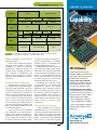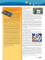
1
FPGAs Pile on Power in Configurable Processing The magazine of record for the embedded computing industry October 2007 www.rtcmagazine.com Safety-Critical Beyond Reliability Systems to Safe Operation An RTC Group Publication Manage Even Small Modules via the Web Solid-State Memory Takes on Big Jobs GE Fanuc Embedded Systems MicroTCA™ minus the surprises. Application-ready platforms take the ‘time’ out of time to market. The process of getting a hardware platform up and running can be full of nasty little surprises, like cooling issues, interoperability problems, power distribution challenges and even component availability. Unless, of course, you choose a pre-validated, pre-tested and pre-integrated MicroTCA™ platform from GE Fanuc Embedded Systems. We spend a lot of time putting the system together for you, so you can spend your time fine-tuning your applications. With one of our systems, you can jump right in, knowing that all the cards speak to each other and to the MCH, that the OS and drivers work, that the IPMI functions flawlessly and that you just got a huge jump on your competition. To make things go even smoother, we have developed one of the biggest selections of AdvancedMC™ cards on the planet. Everything from Cavium Octeon™ packet processors to Intel® Pentium® M processors, Gigabit Ethernet to OC-12, and VGA to GPS. With our pre-validated systems and AdvancedMC selection, the only surprise you may encounter is just how easy MicroTCA can be. MicroTCA 2000 Prevalidated Modular Platform www.gefanucembedded.com/microtca © 2007 GE Fanuc Embedded Systems, Inc. All rights reserved. TABLEOF CONTENTS OCTOBER 2007 Departments 5 Editorial Embedded Interconnects Are Winding Down to the “Magic Three” Insider 7 Industry Latest Developments in the Embedded Marketplace Views and Comment 64 News, Alive, Well, Small and Rugged & Technology 48 Products Newest Embedded Technology used by Industry Leaders Technology in Context Configurable Processing Platforms Deliver for 10 FPGAs Next-Generation Signal Processing Systems Craig Sanderson, Nallatech Safety-Critical Systems Open FPGAs to 14 Tools Expand into New Domains Beyond Reliability to Safe Operation Rick Kuhlman, National Instruments Derek Palmer, Xilinx Cover Photo: Courtesy of RobotWorx: http://www.robots.com Solutions Engineering Remote Monitoring and Management and Trade-Offs 20 Alternatives for Remote Monitoring and Management of Embedded Devices Rahul Shah, Lantronix 16 Industry Insight 31 Xilinx XtremeDSP Solutions Starter Platform Solid-State Storage Not Just for Consumers 32 Flash: Anymore Battery-Free Wireless Communication Technology Kelly Stone and Woody Hutsell, Texas Memory Systems Software and Development Tools Safety-Critical Systems 48 iEEE-1394-(Firewire) Board in PC/104-Plus Format 61 Flash Memory in 36 Managing Safety-Critical Devices Randy Martin, QNX Software Systems Safety in 42 Implementing Real-Time Systems with NonLong-Life ATX Motherboard with RAID Volatile Memory Technology Rich Paulson, Simtek Digital Subscriptions Available at www.rtcgroup.com October 2007 OCTOBER 2007 Publisher PRESIDENT John Reardon, johnr@r tcgroup.com EDITORIAL DIRECTOR/ASSOCIATE PUBLISHER Warren Andrews, warrena@r tcgroup.com Editorial EDITOR-IN - CHIEF Tom Williams, tomw@r tcgroup.com MANAGING EDITOR Rebecca Bauer, rebeccab@r tcgroup.com COPY EDITOR Rochelle Cohn Art/Production CREATIVE DIRECTOR Jason Van Dorn, jasonv@r tcgroup.com ART DIRECTOR Kirsten Wyatt, kirstenw@r tcgroup.com GRAPHIC DESIGNER Christopher Saucier, chriss@r tcgroup.com DIRECTOR OF WEB DEVELOPMENT Marke Hallowell, markeh@r tcgroup.com WEB DEVELOPER Brian Hubbell, brianh@r tcgroup.com Advertising/Web Advertising WESTERN REGIONAL ADVERTISING MANAGER Stacy Gandre, stacyg@r tcgroup.com (949) 226 -2024 WESTERN REGIONAL ADVERTISING MANAGER Lauren Hintze, laurenh@r tcgroup.com (949) 226 -2014 EASTERN REGIONAL ADVERTISING MANAGER Nancy Vanderslice, nancy v@r tcgroup.com (978) 443 -2402 The magazine of record for the embedded computing INSIDE SALES MANAGER Carrie Bowers, carrieb@r tcgroup.com (949) 226 -2029 Billing industry The magazine of record for the embedded computing industry Mag gie McAuley, mag giem@r tcgroup.com (949) 226 -2024 To Contact RTC magazine: Free Online www.rtcmagazine.com Spotlighting the Trends and Breakthroughs in the Design, Development and Technology of Embedded Computers. Search Archived Editions along with the Latest News in the Embedded Community. www.rtcmagazine.com HOME OFFICE The RTC Group, 905 Calle Amanecer, Suite 250, San Clemente, CA 92673 Phone: (949) 226-2000 Fax: (949) 226-2050, www.rtcgroup.com EASTERN SALES OFFICE The RTC Group, 96 Dudley Road, Sudbury, MA 01776 Phone: (978) 443-2402 Fax: (978) 443-4844 Editorial Office Warren Andrews, Editorial Director/Associate Publisher 39 Southport Cove, Bonita, FL 34134 Phone: (239) 992-4537 Fax: (239) 992-2396 Tom Williams, Editor-in-Chief 245-M Mt. Hermon Rd., PMB#F, Scotts Valley, CA 95066 Phone: (831) 335-1509 Fax: (408) 904-7214 An RTC Group Publication October 2007 Published by The RTC Group Copyright 2007, The RTC Group. Printed in the United States. All rights reserved. All related graphics are trademarks of The RTC Group. All other brand and product names are the property of their holders. OCTOBER 2007 EDITORIAL Embedded Interconnects Are Winding Down to the “Magic Three” by Tom Williams, Editor-in-Chief A dvances in computer technology often seem like a game of juggling bottlenecks. If processor performance seems too slow, the industry comes out with higher-speed CPUs. Then, of course, operating systems and applications see the increased potential and add features, which demand more memory. Then transferring data becomes a hurdle and we get advances in interconnects. These steps are accompanied by tons of white papers, market studies and oceans of PowerPoint slides—but inexorably the world advances. These periods of intense activity, innovation and hype are usually interspersed with intervals that can informally be referred to as “shake-out” times. That is, when a number of competing approaches have been put forward, engineers, marketers, users and OEMs evaluate, use, experiment, improve and ultimately adopt or reject them. We appear to be in such a period in terms of interconnects. Remember back several years ago when serial switched fabrics hit the scene? Initially there were over 100 of them thrown up against the wall. Think back now and see if you can name six of them (cue the Jeopardy music). Well, don’t feel bad—you’re only going to need to remember three interconnect technologies for the foreseeable future: Ethernet, PCI Express and USB. The rest are falling by the wayside or crawling into niches to eke out a limited existence. Ethernet should come as no surprise. It has been ubiquitous for many years, dominates both wired and wireless LANs and connects us all to the Internet. TCP/IP now takes us—via IPv6— from the Web all the way to individual sensors and actuators. Practically every CPU board sold today has at least one Ethernet connection and these are commonly offered as 10, 100 or 1000 Mbit/s speeds. 10 Gigabit Ethernet is now becoming more widespread and higher speeds are in the future. Ethernet connectivity enables embedded Web servers to provide remote monitoring and control of devices large and small and in large numbers. Ethernet is here to stay. A less obvious but nonetheless solid victory is being achieved by PCI Express (PCIe). At first it seemed an “also ran” among such competitors as Star Fabric, HyperTransport, RapidIO and InfiniBand See? I named four! Its hidden advantage, however, was backward compatibility with the PC-based PCI interconnect and the attendant economies of scale that come with the PC market. Gen2 PCIe is about to break into the world with 5 Gbit/s speeds per lane, and 10 Gbit/s Gen 3 will eventually follow. It was once a truism to think that PCIe was fine as an interconnect between components and boards “inside the box,” but to go between chassis you needed a different interconnect, most prominently InfiniBand. Now, however, that is changing. PCI Express over cable, pioneered by One Stop Systems, lets systems communicate up to seven meters between chassis. In addition, I/O and clustering using PCIe switches being introduced by Dolphin will enable fiber-optic connections of at least 300 meters between nodes. Not only that, One Stop’s SuperSwitch technology will enable PC-to-PC networking via nontransparent bridging between CPUs on a backplane or among boxes. Why, then, would anyone use InfiniBand when an all-PCIe solution is at hand? And then there’s USB. USB 2.0 is already finding its way into the embedded space, most recently in the form of Stackable USB developed by PC/104 maker Micro/sys. But it is showing up in other forms as well, driven, again, by economies of scale, lowcost components and software compatibility. Now, Intel, HP, TI and other companies have formed a group to promote USB 3.0, which will have speeds approaching 5 Gbits/s and will significantly reduce power consumption, yet be backward compatible with previous USB specs. Add to this the just-beginning deployment of Certified Wireless USB, and the potential for low-cost, high-speed peripherals, both wired and handheld, takes a quantum leap. These developments in the world of interconnects also fuel the trend toward the use of small form-factor boards, which are primarily PC-based. This means that most of them incorporate PCIs as well as Ethernet as a matter of course. USB can and will be included as needed, but will perhaps not be as universal. The pervasive growth of embedded PC-compatible small modules can be expected to make the “magic three” interconnect technologies even more common. October 2007 THE ADVANTAGES ARE CLEAR Motorola is the clear choice for MicroTCA™. Motorola’s cutting edge MicroTCA products can help cut your costs, risk and design cycle while increasing your flexibility. Whether your applications need specific I/O, flexible packaging, ruggedization or a choice of processors, we can customize solutions to meet your needs. That’s why our MicroTCA products are quickly being adopted for network-centric applications across telecommunications, defense, aerospace, industrial and medical industries. Looking for a clear advantage over the competition? HELLOMOTO™ See why Motorola should be your first choice for MicroTCA solutions at: motorola.com/computing/MTCA MOTOROLA and the Stylized M Logo are registered in the US Patent & Trademark Office. MicroTCA and the MicroTCA logo are trademarks of PICMG. All other products or service names are the property of their respective owners. © Motorola, Inc. 2007. All rights reserved. IndustryInsider OCTOBER 2007 Small Form-Factor Trade Group Formed to Address Emerging Technologies Emerson Acquires Motorola’s Embedded Communications Computing Group Five companies have announced the formation of a new standards group focused on small form-factors. The group, named the Small Form-Factor Special Interest Group (SFF SIG), has Emerson has announced that charted a course to develop, adopt and promote circuit board specifications and related technoloit will acquire Motorola Inc.’s Emgies that will help electronics equipment manufacturers and integrators reduce the overall size of bedded Communications Comtheir next-generation systems. The founding companies are: VIA Technologies, WinSystems, Samputing (ECC) business for $350 tec, Octagon Systems and Tri-M Systems and Engineering. The group says it does not compete million. St. Louis-based Emerwith existing trade organizations and that its purpose is to address new market needs as well as son manufactures appliances and specifications that are not yet managed by a trade group. tools; electronics and telecomThe group’s intention is to embrace the latest technologies, as well as maintain legacy compatmunications equipment; industrial ibility and enable transition solutions to next-generation interfaces. New technologies available to automation and process control systems; and heating, ventilating long-lifecycle system and device manufacturers include lower-power and highly integrated procesand air conditioning equipment, sors, chipsets and memory based on 90with nmtechnology and 65 nm Get Connected andprocesses, higher-density connectors but has become increasingly active companies providing solutions now with improvements for ruggedness, and high-speed serial interfaces such as PCI Express, Serial in the embedded computing arena Get Connected is a new resource for further exploration ATA (SATA) and USB 2.0, which replace slower and space-consuming parallel interfaces. Some of through acquisitions. into products, technologies and companies. Whether your goal these components were announced and displayed this week at ESC. Motorola’s ECC business, is to research the latest datasheet from a company, speak directly The SFF SIG has formedEngineer, threeorworking address product categories. The with an Application jump to a groups company'stotechnical page,different the which had 2006 revenue of about SBC Workinggoal Group discussing new small form-factor board computers. The Modules of GetisConnected is to put you in touch with the rightsingle resource. $520 million, provides embedded Whichever level of service you require for whatever typesmall of technology, Working Group is developing a specification for a new computer-on-module (COM) form faccomputing products and services Get Connected help youisconnect with the approaches companies and products tor. The Stackables WorkingwillGroup examining to embrace new high-speed serial to communication infrastructure you are searching for. and equipment manufacturers in technologies into legacy systems in a smooth manner that preserves investments in I/O, cabling www.rtcmagazine.com/getconnected telecommunications, medical imand enclosure designs. The initial members would like to solicit input from system manufacturers aging, defense and aerospace and and integrators in order to ensure that specifications serve the end-user community as fully as industrial automation. Tempe, possible. Arizona-based ECC has approxiThere are two membership categories for the SFF SIG. Voting members are involved in promately 1,100 employees. The deal, moting, supporting and developing specifications for small form-factor boards, components and which is expected to close by the Get Connected technology and companies providing solutions now SFF SIG for systems. In addition, voting memberswith review specifications that are submitted to the end of the year, will make Motoroadoption. Non-voting provide internalintospecification development, andWhether la’s Getmembers Connected is a newinputs resourcedirectly for furtherto exploration products, technologies and companies. yourECC goal isbusiness to research theof latest part Emerson datasheet from aprior company, speak directly with Engineer, or jump to a company's technical goal of Get Connected is to putalso you can view these specifications to publication, butandoApplication not cast approval votes. For more infor-page, the Network Power. That division in touch with the right resource. Whichever level of service you require for whatever type of technology, acquired Artesyn Technologies a mation, visit www.sff-sig.org. Get Connected will help you connect with the companies and products you are searching for. little over a year ago. www.rtcmagazine.com/getconnected David Farr, chairman, chief Group Forms to Develop go” transfer applications in the vice polling to a technique that lets executive officer and president of Super-Speed USB PC and consumer market, but ina device remain idle until traffic Emerson, said in a statement, “The Interconnect evitably an interconnect with such appears for it on the USB network. combination of Motorola’s ECC A group of six major industry speed, compatibility and econoIn addition, there are a number of business with the $100 million companies has formed the USB mies of scale will find its way into improvements planned in the new embedded computing business 3.0 Promoter Group to create a the embedded arena. specification to reduce power conwe acquired as part of Artesyn USB interconnect that can deliver Its utility for media, however, sumption. A completed USN 3.0 last year establishes Emerson as a 10 times the speed of today’s USB is undeniable. During a session at specification is expected by the leader in the embedded computing 2.0 connection. Since that connect the recent Intel Developer Forum first half of 2008 with first impleindustry. Through this transaction, speed is currently 480 Mbits/s, in San Francisco, the favorite exmentations in the form of discrete Emerson can provide greater cathis would mean a speed of apample was the ability to download silicon. Products based on the new pabilities to our customers as they proximately 4.8 Gbits/s—which a 27 Gbyte high-definition movie interconnect may appear as early Get Connected with companies and adopt advanced new technologies Get Connected is within hailing distance of Gen2 in about 70 seconds as opposed to as mid-2008. products featured in this section. with companies mentioned in thisand article. expand applications for their PCI Express with 5 Gbits/s. The the 14 to 15 minutes it takes with www.rtcmagazine.com/getconnected www.rtcmagazine.com/getconnected customers.” six companies are Intel, HewlettUSB 2.0. USN 3.0 will be backPackard, Microsoft, NEC, NXP ward compatible with the previSemiconductors and Texas Instruous USB technologies and their ments. The group is targeting the plug and play capabilities, but will Get Connected with companies mentioned in this article. design initially for fast “sync-andmove from their technique of dewww.rtcmagazine.com/getconnected Get Connected with companies and products featured in this section. Ad Index Products End of Article www.rtcmagazine.com/getconnected October 2007 Industry Insider QNX Publishes Neutrino Source Code and Opens Development Process QNX Software Systems has announced that it is opening access to the source code of its QNX Neutrino real-time operating system under a new hybrid software licensing arrangement. QNX will make source code for its microkernel-based OS available for download. The first source release includes the code to the QNX Neutrino microkernel, the base C library and a variety of board support packages (BSPs) for popular embedded and computing hardware. Not only can developers view the QNX Neutrino source code, but they can also improve, modify, or extend that code for their own purposes or for the QNX community at large. They can then choose to offer back those changes to QNX Software Systems and the QNX development community or keep their modifications private and proprietary. These changes are part of a new hybrid software model created by QNX that supports the customer’s goal of profiting from software while fueling the passion for developing it. Access to QNX source code is free, but commercial deployments of QNX Neutrino run-time components still require royalties, and commercial developers will continue to pay for QNX Momentics development seats. However, noncommercial developers, academic faculty members and qualified partners will be given access to the QNX development tools and run-time products at no charge. Customer and community members will also have the ability to participate in the QNX development process, similar to projects in the open source world. Through a transparent development process, software designers at QNX will publish development plans, post builds and bug fixes, and provide moderated support to the development process. They will also collaborate with customers and QNX community, using public forums, wikis and source code repositories. QNX has also introduced a new community portal Web site, called Foundry27, as the new hub for its transparent development initiative. At Foundry27, customers and developers can access a wealth of resources relating to the QNX Neutrino RTOS and the QNX Momentics IDE, as well as to new community projects. Upon completing the free registration, users then identify which of three different software licenses is appropriate to their interests and gain immediate access to copies of most QNX software products, as well as source code for many of these components. graphical system design environment in which to design, prototype and deploy their projects. The NI Embedded Systems Laboratory uses NI technologies to provide embedded system design experiential research opportunities for upper division undergraduate and graduate students. All students in the UC Berkeley EECS department, which recently was ranked No. 2 in the nation in U.S. News & World Report’s undergraduate and graduate college rankings, will work in the lab using NI products. In addition to combining undergraduate and graduate courses, this lab brings together members of the UC Berkeley community, including student and postdoctoral researchers and faculty from a variety of departments. The new lab offers a rich and open environment that students can use to explore all aspects of embedded systems design, from core concepts such as models of computation, concurrency and tool-supported design method- New National Instruments Embedded Systems Laboratory at UC Berkeley National Instruments and the University of California, Berkeley, College of Engineering are working together to offer electrical engineering and computer sciences (EECS) students a new 3%.3/2!9 %MBEDDED%LECTRONICS USEDHERE #ONTROLWATERLEVELS -EASURETEMPERATURE -ONITORDENSITY #APTUREHIGHRESOLUTIONIMAGES INREALTIME #APTUREVIDEOVIA%THERNET !NALYZEMOTION /NSCREENDISPLAYOFTEXTANDGRAPHICS WECANEVENDOTHIS 3%.3/2!9DESIGNSANDMANUFACTURES/%-ELECTRONICSFORVIDEOIMAGINGDATAACQUISITIONANDMACHINECONTROL /URPRODUCTSINCLUDE&RAME'RABBERS6IDEO3ERVERS)NDUSTRIAL)/VIA%THERNETAND!$$!BOARDS )FYOUCANTFINDWHATYOURELOOKINGFORWEPROVIDECUSTOMSOLUTIONS3%.3/2!9COM\ 4&/403": EMBEDDED ELECTRONICS &2%%DAYEVALUATIONS&2%%YEARWARRANTYAND&2%%LOCALTECHNICALSUPPORT October 2007 Untitled-15 1 9/12/07 5:14:40 PM Industry Insider ologies to sensors and actuators, data acquisition, interfacing and real-world applications such as mechatronics, robotics and controls systems. Students will focus on RF, embedded systems design, test and mechatronics topics while receiving real-world experience in the design, prototyping and deployment stages of embedded systems. The lab includes 12 workstations, and four of those offer NI PXI chassis with modular instrumentation including arbitrary waveform generators, digitizers, multimeters, power supplies and USB data acquisition hardware. New PICMG COM Express Plug and Play Subcommittee Formed Adlink Technology, Congatec and MSC, have joined together to form a new PICMG COM Express plug and play subcommittee. The to-be-released “COM Express Plug and Play Design Guide” aims to increase the use of COM Express modules by defining a set of carrier design guidelines that enable plug and play support and increase compatibility between COM Express modules from various vendors. Jeff Munch, CTO of Adlink Technology and interim chairman of the new subcommittee, expects this new PICMG carrier board design specification to release in February 2008. After the release of the PICMG COM Express specification (COM.0), several manufacturers have filled the marketplace with a wide variety of COM Express modules. It soon became apparent that a plug and play specification was required to mitigate carrier board incompatibilities. Therefore, Adlink, Congatec and MSC applied to the PICMG group for the creation of a subcommittee to define a “COM Express Plug and Play Design Guide” to increase adoption of the COM.0 standard through a plug and play carrier board design specification. Congatec started the COM Express PnP Initiative, which focused on carrier board design. Now this initiative has further evolved to address the incompatibilities seen between different vendors using proprietary carrier board designs by providing a definite specification to increase and streamline the adoption and use of COM Express products. Warning over Hacking Kits for Sale on eBay Tier-3, a behavioral analysis IT security specialist, has warned companies that hacker toolkits— which were previously confined to specialist hidden forums on the Internet—are now being sold openly on auction sites such as eBay. “This is a serious development,” said Geoff Sweeney, Tier3’s CTO, who added that, where previously would-be hackers had to score “brownie points” to gain access to the hacker forums and source the kits, the fact that they are now on open sale on eBay is very worrying. “It basically puts high-level hacking tools, including surreptitious Trojan loaders and Web site hacking utilities, into Untitled-4 the hands of almost any Internet user—including novices—providing they have an eBay and PayPal account,” said Sweeney. Sweeney went on to say that the hacker kits are usually sold on eBay as ethical hacker training courses, but the courses also include a wealth of utilities for “educational purposes.” “This is really bad news for companies of all sizes, as it means they have to be extra careful on the IT security front. As we’ve said before, companies can no longer rely on a single line of defense for their IT resource and now need to consider extending their security umbrella to include behavioral analysis technology,” he said. “Only then can they have a safety net capable of intercepting both known and unknown electronic attacks on their IT systems,” he added. 1 Untitled-6 1 10/8/07 11:51:05 AM October 2007 10/8/07 1:16:08 PM Technology InContext configurable processing platforms FPGAs Deliver for Next-Generation Signal Processing Systems For speed, flexibility, small size and interconnect options, today’s latest generation of FPGAs is the more frequent choice for high throughput systems and for moving the digital stages of processing closer to the analog signal source. by C raig Sanderson Nallatech C omplex signal environments are placing increasing performance demands on embedded digital signal processing (DSP) systems. Signal processing applications including satellite communications, radar, software defined radio (SDR) and signal intelligence require ever higher computing performance and I/O bandwidth. This needs to be delivered with lower power consumption and on platforms that can quickly transition from the R&D lab to deployed systems, often in harsh environments. The latest signal converter technologies and signal processing trends are increasing the demand on processing engines. Advances in signal conversion technologies are resulting in higher resolution and sampling rates of digitized signals. In modern signal processing systems, current trends are to move processing into the digital domain. This means that multiple channels of high-bandwidth data must be processed directly sampled from analog front-ends. Both of these factors mean that there is more data to be processed faster. Today, FPGAs are the mainstream technology of choice for many new signal processing systems. Ten years ago, many would have considered FPGAs to be a niche “disruptive technology.” This transition has reshaped the competitive landscape of commercial-off-the-shelf (COTS) hardware and software. An ecosystem of new companies 10 October 2007 offering COTS FPGA processing solutions and professional design services has flourished. Established players with product portfolios built around RISC processor technologies have evolved their product offerings to include both processors and FPGAs. Industry-standard form-factors and interconnect technologies are the mainstay of the embedded systems world. Organizations such as VITA and PICMG develop open modular standards for embedded computer systems. Equivalent organizations exist in the interconnect space, developing standards for cable and backplane communication. Over the past few years, the standards landscape has changed dramatically. VITA and PICMG have been busy updating existing standards such as VME and cPCI to meet the demands for the embedded market. Brand new standards such as VPX and ATCA have been introduced. Products using these standards can be used to deliver complex signal processing systems using commercial products, as we will demonstrate with an example. Signal Processing System Trends Until relatively recently, the initial stages of signal processing systems were performed in the analog domain. Processing digitized analog signals in the digital domain offers a number of important ben- efits. Digital processing of digitized analog signals offers robust system stability, flexibility in waveform and filter design, the ability to develop adaptive processing algorithms and an effective upgrade path. These benefits have driven the trend to move the A/D converter closer to the antenna in the signal processing chain and perform more processing in the digital domain. Generally, this means that A/D signal converters now input raw digitized data directly into the processing stage of the system. The data resolution and sampling frequencies of such A/D converters are increasing dramatically. High-resolution converters sampling in the multi megasample per second (Msample/s) and gigasample per second (Gsample/s) range are now commonplace in many systems. The benefit of higher sampling rates is somewhat obvious in that developers are able to sample much higher analog signal frequencies. The need to sample these higher analog frequencies is driven by the needs of applications including the latest radar and signal intelligence systems. The higher resolution of the A/D converters is driven by the need for improved digital representation of the analog signal. Another benefit of higher resolution converters is that they function better in the analog realm, allowing designers to reduce the board design complexity while maintaining accuracy and performance. Technology InContext It is worth looking at a few examples to gauge the impact of these higher sampling rates and resolutions. The current highest sampling rate converters operate in the 3 Gsample/s range, at a resolution of 8 bits. This means that the data bandwidth of a single channel is 3 Gbytes/s. Looking at higher resolution converters, 16-bit converters are being designed into many systems. Current sampling rates for these converters are around 130 Msamples/s, with 250 Msample/s devices around the corner. 16 bits at 250 Msamples/s equates to 500 Mbytes/s per channel for the digitized data. These very high data bandwidths represent just a single channel. Example card level configurations demonstrate that this problem just keeps on growing when you get to the card level. Four channels of 8bit/3 Gsamples/s on a single card gives a front-end data bandwidth of 12 Gbytes/s. The equivalent data bandwidth for 8 channels at 16-bit/250 Msamples/s would be 6 Gbytes/s. To put into some context, consider that each example is considerably more data than that on a single 4.7 Gbyte DVD—every second. Now consider how long it takes for a new dual-core processor desktop computer to open or even just move a file 1000 times smaller that that and the scale of this processing challenge becomes clear! Enhanced DSP Performance with FPGAs Handling the bandwidth of data from analog front ends as described above is a huge challenge. The focus tends to be on processing such large volumes of data in real time. A second less obvious challenge is moving the data—getting digitized data onto a processor and interprocessor communication of either raw data or results. FPGAs are able to handle both the processing and I/O requirements of directly coupled analog front ends. For this reason, the FPGA is now the de facto choice for most high-performance signal processing systems. From a processing perspective, the realtime processing of high-bandwidth digitized signal data can be tremendously challenging. Complex DSP algorithms that can include digital filters, digital down converters, spectrum analyzers and demodulators among others need to be implemented in real time. Traditional processors such as RISC or DSP processors have a single ALU that can perform all the calculations for a Figure 1 The Xilinx Virtex-5 SXT devices range in logic density from 35,000 to 95,000 logic cells and have 192 to 640 dedicated DSP48E slices that can deliver 352 GMACs at 550 MHz. The DSP48E slice includes a 25x18-bit multiplier, a 48-bit second stage for accumulation and arithmetic operations, and a 48-bit output that can be expanded to 96 bits. The devices also include 8 to 16 RocketIO GTP Low-Power Transceivers capable of operation in the 100 Mbit/s to 3.75 Gbit/s range. These devices support over 40 I/O standards with 360 to 640 Maximum Select I/O pins. given application sequentially. Only one arithmetic function (e.g., a multiply) can be completed at one instant in time, meaning that external memory accesses for the storage of sub-products present an additional overhead. Newer multicore processors and specialized processors such as the CellBE have multiple ALUs and can therefore do multiple calculations simultaneously. However, these still rely on a relatively small number of ALUs running very fast, and storing sub-products in external memory. FPGAs are different. When used in a processing context, FPGAs can be considered to be custom processors. Designs with tens or hundreds of ALUs can be implemented, with distributed high-speed internal memory available for sub-product storage. This means that multiple arithmetic functions can be implemented simultaneously, resulting in highly efficient application implementations. Performance depends on the application being implemented, but is generally in the range of ten to a hundred times faster than a processor on a single device basis. FPGAs are therefore ideally suited to the implementation of complex DSP algorithms required in signal processing systems. The latest generations of FPGAs offer ever better processing performance compared to older devices. As the market for FPGAs in DSP systems has grown, vendors have also started to add new features to offer enhanced DSP performance. The latest Xilinx Virtex-5 SXT FPGA family is a good example of this and is optimized for DSP and memory-intensive applications. The SXT family includes dedicated features for DSP applications, including new high-performance architecture, up to 8.7 Mbits of 550 MHz on-chip memory and up to 640 embedded DSP blocks that can implement a variety of functions (Figure 1). These resources provide higher performance, versatility and efficiency with reduced power consumption for signal processing applications. DSP systems require I/O to support direct connection of A/D converters and for interprocessor or system-level communications. Most A/D converters require general-purpose single-ended or differential I/O lines, and some high-end devices are emerging with direct serial connection. For system-level and interprocessor communications, support for common device and board-level interfaces are required. The majority of the latest FPGAs can address both of these requirements. FPGAs have large quantities of general-purpose I/O lines, to which A/D converters can be directly connected. With onboard serial transceivers, built-in support is also provided for common interfaces such as PCI, PCI Express, Ethernet and Serial RapidIO. These interfaces can be used to distribute data between multiple FPGAs, which allows large algorithms to be split across multiple FPGAs. Complex algorithms, such as the shared product calculations used in many radar systems, can also be handled using these high-bandwidth interprocessor communication fabrics. Building Compact Signal Processing System Using FPGAs A DSP-based radar processing system built with the goal of capturing and processing a 1 GHz bandwidth may need a sampling rate of 3 Gsamples/s with an 8-bit sample. Postprocessing would require multiple FPGAs. One approach would be to build a dedicated piece of hardware to implement this system. Assuming all of the correct resources were in place, this would take October 2007 11 Technology InContext VXS Front Panel MMCX CH0 MMCX CH1 ADC ADC MMCX TRIG Gigabit Ethernet RS232 MMCX CLK Boot Flash CLK MGMT Xilinx Virtex-5 SX95T MPC8548E PowerPC Processor 256MBytes SDRAM 2x GTP x4 Xilinx Virtex-5 SX95T ADC ADC MMCX TRIG Xilinx Virtex-5 SX95T PCI-X 133 SRIO x4 XMC P4 SRIO x4 SRIO x4 Xilinx Virtex-5 SX95T 256MBytes SDRAM Intel® 852GM + ICH4 chipset / DDR2 memory up to 1GB / 10/100 Ethernet / Dual channel 18-bit LVDS LCD panel / 4 x PCI support / ISA support / 2x IDE / 4 x USB/ 2 x RS-232 AMD LX-800 500MHz AMD LX + AMD CS5536 chipset / 8 x COM / Ethernet / 4 x USB / Windows CE 6.0 OPC Modbus support library provide by SDK/ ideal to work with PLC, industrial communication converter/gateway, and factory automation Intel Core 2 Quad Mini-ITX KINO-9654G4 Mini ITX Ideal for High performance computing or network appliance Intel Core 2 Extreme, Core 2 Quad CPU / DDR 2 memory / 4 Gigabit Network / 6x USB / 2xGbE / 4x RS-232 / 1x PCI express expansion / 7.1 Channel Audio http://www.ieiworld.com [email protected] 1-866-276-6754 Tel :1-909-595-2819 12 Untitled-1 1 October 2007 Fax: 1-909-595-2816 10/18/07 10:50:24 AM XMC Mezzanine 8MBytes SRAM 256MBytes SDRAM GPIO 80 Lines P4 BP GPIO 28 Lines FPGA GPIO 4 Lines Gigabit Ethernet RS232 2x SRIOx4 VME64 2eSST FPGA GPIO 4 Lines P4 BP GPIO 28 Lines VXS Backplane Figure 2 Fanless AMD LX-800 Universal Controller 256MBytes SDRAM 256MBytes SDRAM 256MBytes SDRAM Socket M Intel® Celeron M 1.0GHz CPU CLK MGMT 2x GTP x4 SRIO Switch 8MBytes SRAM MMCX CLK 256MBytes SDRAM VME-PCI Bridge XMC Mezzanine XMC P4 MMCX CH3 256 MBytes SDRAM 256MBytes SDRAM ETX form factor single board computer NANO-9452 MMCX CH2 A high-speed radar processing system can be built using a VPX backplane board and two XMC mezzanine cards, all based on four instances of the same FPGA with appropriate IP in each. at least 12 months and cost hundreds of thousands, if not millions of dollars. Commercial solutions such as this are available off the shelf and offer low risk and faster time-to-market than custom solutions. An equivalent system built using commercial FPGA hardware and IP cores illustrates the benefits of using signal processing systems featuring multiple A/D converters with attached scalable FPGA-based architectures as opposed to using customized solutions. The forthcoming VXS-610 and XMC210 products from Nallatech could provide such a solution. The VXS-610 is a VXS-based FPGA and PowerPC-based compute card that features two Xilinx Virtex-5 FPGAs, a PowerPC and two XMC mezzanine slots. The XMC-210 is an FPGA and data acquisition XMC mezzanine that provides FPGA processing and data acquisition capability, with dual channel 8-bit, 3 Gsample/s A/D functionality and a single Xilinx Virtex-5 FPGA. A configuration of one VXS-610 and two XMC-210s is shown in Figure 2. The configuration in Figure 2 can handle four incoming analog data streams and digitize them simultaneously at 3 Gsamples/ s. Channels 0 and 1 communicate digitized data directly into one of the XMC FPGAs while channels 2 and 3 come on the other XMC. This data can initially be processed in the XMC FPGAs before it is communicated to the FPGAs on the VXS card for further processing. The high-speed communications link between the FPGAs enables processing of intermediate products from multiple channels on the same card. Since the FPGAs are connected directly into the high-speed Serial Rapid IO communications fabric, this interchannel processing can be extended to channels across multiple cards. The latest generations of commercial hardware featuring multiple A/D converters with scalable FPGA-based processing systems permit the design and fielding of compact systems to handle both the increased data load and processing requirements of today’s complex sensor processing systems. Front-end processing using FPGAs tightly coupled to multiple A/D converter channels can dramatically reduce the amount of data that must be transmitted across a system. Complex real-time processing applications such as radar, SDR and signal characterization can be processed within the FPGA fabric at close proximity to the sensor, resulting in a significant simplification of system architecture while improving overall performance. Nallatech Eldersberg, MD. (410) 552-3352. [www.nallatech.com]. Technology InContext configurable processing platforms Tools Open FPGAs to Expand into New Domains As FPGAs have become faster, denser and more complex, a new generation of graphical development tools has risen to make their power accessible to scientists and engineers to address their projects without detailed knowledge of hardware design. by R ick Kuhlman, National Instruments and Derek Palmer, Xilinx T he acceptance of field-programmable gate arrays (FPGAs) in a wide range of market segments has grown because of the constant improvement of silicon device technology and features. Once relegated to the simple glue logic domain and designed by hardware engineers, FPGAs now can implement entire systems on a chip (SoCs) designed by engineers and scientists in a variety of different disciplines. Similarly, software tools used to develop FPGAs have undergone radical changes, which empower these same engineers to innovate. FPGA development software has expanded out of the pure hardware domain into the SoC and even market-specific domains. FPGAs are no longer the choice of only hardware engineers. Software engineers, mechanical engineers, biologists, digital signal processor (DSP) algorithm developers and embedded programmers now design with FPGAs. In the early ’90s, for example, engineers were creating programmable logic designs with 12 logic cells in a device on a 3 micron fab process with a 95 ns input to output delay. They captured these designs in simple schematic capture tools and handled logic synthesis and device place and route with software on a stack of 5½-inch floppy disks sequentially fed into a 4 MHz PC as requested. Often the tools failed in synthesis, and these engineers would have to retrieve their pencils and graph paper, fill out state diagrams and convert them to Karnaugh 14 October 2007 Figure 1 LabView graphical programming targets Xilinx FPGAs on off-the-shelf hardware. maps; find their minterms or maxterms; and extract a minimized sum of products (SOP) equation. If it got complex, they would try the Quine-McCluskey algorithm. Given the size of the design, this was not a difficult task though it required skills unfamiliar to non-hardware engineers. Soon engineers were developing TTL library elements to help designers more quickly build systems. Instead of using single flip-flops and NAND gates, designers could drop down hundreds of gates by selecting a few 74169 counters or 74139 demultiplexers. The development of more abstract libraries has continued since. Fast-forward five years to when FPGAs had grown to a few thousand logic cells, making them capable of implementing complex systems—not just glue logic. Silicon technology had advanced to 1.8 microns, performance had more than quadrupled, and costs had dropped dramatically. Driving cost down drove up the adoption of FPGAs by a much broader consumer base. At the same time, ASIC costs were growing. NRE costs, EDA tool costs and growing labor costs started to drive ASIC design starts down, making the cost of ownership of FPGAs very at- One-Stop Shopping Bring Us Your List Everything you need for your CompactPCI® Applications Performance Technologies’ CompactPCI® products and solutions are the industry’s most capable and complete open-standards offerings for telecom, aerospace and defense, and commercial applications. We create innovative and robust solutions that enable you to get your products to market faster. Our integrated solutions include: Advanced Managed Platforms™ : These flexible, scalable platforms are ideal for a wide range of compute-intensive applications. Coupled with exceptional support services, we have what you need to quickly and cost-effectively develop and deploy your system. High-Performance Blades: Single and dual-core SBCs, Ethernet switches, intelligent shelf management, voice processors, serial and T1/E1 communications I/O, and RAID storage blades. Platforms. Blades. Software. Support. Many solutions. One vendor. NexusWare ® : Our CGL 3.2-registered and POSIX-compliant Linux distribution includes a full operating system, development tools, protocols, HA middleware, and SA Forum-compliant APIs. Best of all, NexusWare's total integration with our blade and platform solutions means you have shorter development cycles. Contact Performance Technologies today and bring us your product development shopping list. Phone: 585.256.0200 www.pt.com/amp E-mail: [email protected] Technology InContext Figure 2 The Xilinx XtremeDSP Solutions Starter Platform enables developers to evaluate and implement digital signal processing systems in an FPGA optimized with hard DSP blocks for high-performance DSP applications. tractive. However, the software tools of the time were still primarily tailored to hardware engineers. VHDL and Verilog had become the predominant design entry method. Unfortunately, the tremendous growth of the FPGA market in the mid1990s slowed the expansion of FPGAs into broader market applications. Instead, FPGAs became very focused on expanding in a few markets such telecom/datacom, networking and communications. This did little to create real disruptive innovation in FPGA development tools. Fast-forward again to the present and a very different FPGA market. Technology has driven FPGA speeds to half a gigahertz and increased their size to more than 300,000 logic cells. What was once an entire circuit board of parts now fits into a single FPGA. Moreover, ASSPlike features have found their way into FPGAs. Entire microprocessor systems, PCI Express, and multi-gigabit transceiver hardware are now available as well. At the end of the dot-com bubble, FPGA companies found themselves actively expanding into new markets after the networking and communications markets had been hit hard. This expansion also created a need to court engineers without hardware backgrounds. Recently, there has been a significant growth in FPGA development 16 October 2007 tool offerings. Tools are now tailored to embedded developers who develop in C language, DSP engineers who develop in hardware, and other engineers and scientists who prefer to work with graphical programming tools. This focus on development tools is what will push FPGA into even more designs as they grow along the seemingly orthogonal vectors of “Ease of Use” and “Powerful.” Higher-level abstraction is the key to success in both areas. The hardware of FPGAs will continue, as it must, to have more I/O in less space, more options with less power, but it is abstraction of the tools that will put the technology within more engineers’ grasp. More specifically, the push for higher levels of abstraction in FPGA programming is predominantly driven by two factors: closing the gap between algorithm designers and FPGA implementations, and making FPGAs viable for engineers and scientists who would not have considered the technology as an option due to programming and system complexity. Perhaps a close third factor is easing the burden on digital designers by abstracting details so they can focus on higher-level, more complex objectives. Although this driver is apparent, it helps the current market—it does not serve to move FPGAs into new markets. A classic issue often plaguing embedded design is the seemingly disconnected tools and thought processes between the “hardware people” and the “software people.” The software silo focuses on the algorithm, optimizing C code to churn the exact answer every time in a sequential fashion. Likening the concept to a puzzle, software engineers place each piece one at a time until the puzzle is complete. When they are done with a fully optimized solution, they hand the code and results to the hardware engineers who must reimplement the problem on an FPGA. Unfortunately, the hardware silo thinks in terms of parallelism and pipelining. Hardware engineers must understand the algorithm fully to optimize it in hardware with a sequentially written algorithm. They think of the puzzle as little subsections put together in a parallel fashion and finally integrated as one complete solution. The increasingly rare engineers who are experts in both silos are bridging the difficult gap that is always trying to widen in this embedded market. The second reason FPGA faces the need for abstraction is the growth of the technology into vertical markets, where the experts are rarely digital designers. Sometimes called “domain experts,” these are engineers and scientists who have a niche idea that requires custom hardware to implement. They understand the algorithms and the IP they need to realize this idea, but they do not have the necessary training and resources for navigating the disconnected world of hardware design, custom board bring up and electrical design considerations. These scientists start companies like SpinX technologies, which pioneered virtual laser valve technology for micro-fluidic applications, or OptiMedica, which built a laser photocoagulation eye surgery machine that works right in the office. Both cases feature highly skilled engineers and scientists in their respective areas, but they could not possibly have every skill necessary to create an entire product based on FPGA technology. Facing time-to-market and price pressures, these scientists believe the more they can do in-house and offthe-shelf the better. Bringing FPGA technology to the micro-fluidic or biomedical application domain is no easy task. Nevertheless these scientists need tools to help LEADERSHIP BUILT ON OVER 40 YEARS OF INNOVATION Four decades of quality manufacturing, design innovation, and process control has earned us the time-honored trust and confidence of a global network of customers. DDC IS YOUR DATA NETWORKING SOLUTION • MIL-STD-1553 COTS Boards and Components • Fibre Channel • Gigabit Ethernet • High Speed 1760 • Enhanced Bit Rate 1553 (EBR) • ARINC 429 Toll Free: 1-800-DDC-5757 www.ddc-web.com All the cards... …for all the solutions Bringing P.A. Semi to PMC, Extreme Engineering Solutions introduces the XPedite8000, the highestperformance, lowest-power PrPMC (Processor PMC) solution available today. With the P.A. Semi PA6T-1682 integrated platform processor, the XPedite8000 offers: • Dual 2.0-GHz Power Architecture processor cores. • Two independent DDR2 SDRAM channels for maximum bandwidth. • Two front-panel Gigabit Ethernet ports. • Two PTMC-compliant P14 Gigabit Ethernet ports. • PCI /PCI-X PMC interface operating at up to 133 MHz. • Linux, VxWorks, and QNX support. For customers looking for one vendor to provide the complete system solution, X-ES provides full component selection, operating system support and integration services. www.xes-inc.com www.xes-inc.com ©2006 Extreme Engineering Solutions [email protected] ©2007 Extreme Engineering Solutions MEN-F-5570 RTC Ad 8/30/07 10:31 AM Technology InContext them meet this challenge from a number of different angles. It is evident that higher levels of FPGA abstraction must exist to narrow the gap between hardware and software and bring FPGA to new applications. “Cto-gate” providers are investing heavily in methods to extract parallelism and generate hardware description languages from code written in software. Other tools attempt to use a combination of sequential programming and configuration-based approaches to target FPGAs with software-like code and user-defined hardware optimizations. One interesting approach to FPGA abstraction is graphical programming. Working in a 2-D space and “drawing” logic to form a dataflow diagram is an excellent way to represent an FPGA circuit. With this approach, engineers and scientists can easily see and implement parallelism, a key advantage of FPGA-based approaches over processors, by drawing their code in multiple parallel paths. Additionally, graphical languages have the advantage of representing the data flow through “wires” rather than instructions. In VHDL, connecting two signals with a trace is an instruction that leads to a physical connection—data_a <= data_b. A graphical language uses a software “wire” to create a hardware connection. Intuitively representing parallelism and data flow is a key high-level feature that makes this type of abstraction uniquely suited for FPGA development. With tools like this, FPGA technology can achieve the objective of reaching new market spaces and domain expert developers. By using graphical system design to design, prototype and deploy their applications, SpinX and OptiMedica were able to use LabView graphical programming and COTS hardware to dramatically simplify development, resulting in complex laser control with an FPGA solution. Presumably, any engineers or scientists can represent the projects they want to accomplish with diagrams. Historically, the market forces them to convert that diagram to sequential textbased code. With graphical languages, the code is a diagram. It is exciting to see FPGA technology getting better, cheaper and faster to design. With its massive growth and distinct benefits, new engineers and new markets are evaluating FPGA possibilities. As mentioned, tools and vendors are beginning to catch up with and identify the bottlenecks causing growing pains in the technology. One example of a collaborative effort to bring FPGA to new scientists and engineers is the partnership between National Instruments and Xilinx to provide a hardware and software platform based on FPGAs. They have worked together to create a number of commercialoff-the-shelf (COTS) FPGA targets with conditioned I/O, standard bus connectivity and LabView as a graphical programming tool for the FPGA logic. LabView, known to many as a graphical programming language for PCs and real-time systems, can also target an FPGA with a block diagram (Figure 1). Through the National Instruments and Xilinx collaboration, the user creates LabView code in this standard graphical programming environment. This graphical code is converted and ported to the Xilinx tools for the compilation procedure rendering a bit file to program the embedded FPGA (Figure 2). Most of the details are taken care of through an abstraction layer offering the user a smooth experience for targeting a true hardware device without the knowledge of VHDL or board-level design. Combined with electronics around the FPGA for analog I/O, digital I/O, clocks and PCI/PXI bus communication (through DMA or register-level), the technology is allowed to grow into vertical markets such that scientists and engineers can utilize the technology effectively. FPGAs will continue to grow because of their flexibility, speed and reconfigurable nature. Because of this, the industry is releasing tools to make this technology not only grow in its traditional market space, but also outside the bounds of previous possibilities, bringing FPGA to the domain expert. National Instruments Austin, TX. (800) 258-7022. [www.ni.com]. Xilinx San Jose, CA. (408) 559-7778. [www.xilinx.com]. The Harsher the Environment, the More You Need MEN Micro! Intel® Pentium®M up to Core™(2) Duo CompactPCI®/Express For the harshest industrial and mobile applications, MEN Micro offers more solutions, including: ■ ■ ■ ■ ■ ■ ■ ■ ■ Core™ 2 Duo T7500 Core 2 Duo T7400, L7400 Core Duo T2500, L2400, U2500 Pentium® M 760, Celeron® M 373 Side cards - UART, multimedia, USB, FireWire, CompactPCI® Express and more! I/O boards - WLAN, GPS, GSM, UARTs, Ethernet interfaces/switches, carrier for M-Modules™, PMC, XMC, PC/104, PC Card, ExpressCard, Mini PCI Compatible 3U Intel® family with scalable computing performance Long-term availability due to easy system adjustment For harsh industrial environments and mobile applications MEN Micro, Inc. RoHS 24 North Main Street COMPLIANT 2002/95/EC Ambler, PA 19002 Tel: 215.542.9575 E-mail: [email protected] www.menmicro.com October 2007 19 Page solutions engineering Alternatives and Trade-Offs for Remote Monitoring and Management of Embedded Devices Monitoring and managing small networked devices presents a number of alternatives depending on whether the idea is to simply monitor or also to control a device over a network, as well as the complexity and the expertise required to implement a solution. d exploration er your goal eak directly al page, the resource. chnology, and products remote monitoring and management by R ahul Shah Lantronix N ed etworking has become widespread networking capabilities as a fundamen- part of its intended use. Once a device is in numerous facets of today’s busi- tal design feature, anticipating connec- network-enabled with an IP protocol, the ness world and consumer market- tion to the Internet and other devices as network is inherently geared for exponenplace. With innumerable types of devices ing; Enterprise-cla and equipment waiting to send and receive ss; S ous Process ta n d utonom A ar d information over a network or the InterXML/RSS HTTPS/SSL/ se m g a e n n a t M a net, the question arises as to how to access nd C SSH Security File and bas Remote ont ro l Database Access and control them. Email HTTP SNMP Size, cost, time-to-market, Internet Interoperable Standards Telnet protocols and supporting resources have (Cisco CLI, PoE) panies providing solutions now ction and Tra been factors that influenced the adopnsf Conne ration into products, technologies and companies. Whether your goal is to research the latest APIs tion of embedded device networking. Ethernet lication Engineer, or jump to a company's technical page, the goal of Get Connected is to put you TCP/IP Having challenges, embedSerial ice you require for whateverfaced type of these technology, Tunneling products have been designed that ies and productsded you are searching for. achieve comprehensive connectivity for devices and equipment to communicate. Employing such technology introduces the task of managing the embedded device connections. er Networking as a Necessity End of Article The motivation to network-enable a product has spread to the extent that almost any embedded device now includes Get Connected with companies mentioned in this article. www.rtcmagazine.com/getconnected 20 XPort Direct Figure 1 October 2007 Get Connected with companies mentioned in this article. www.rtcmagazine.com/getconnected MatchPort b/g WiPort WiPort NR XPort XPort Direct + MatchPort AR XPort AR Embedded device gateways, device servers and programmable device servers offer engineers different feature options for their specific application. It’s essential to understand what you need. PCI-to -PMC Technobox produces custom and off-the-shelf PMCs. Serial Ultra320 FPGA async I/O, SATA, Ethernet, and IDE controllers. Plus a variety of adapters, extenders, and tools for PMC development or integration. Adapters SCSI solutions includes versatile FPGA-based digital I/O, Quad Ethernet Async Our extensive range of Make us your first stop for SATA PMC Solutions. Reconfigurable RoHS CardBus Digital I/O Fast/Wide SAS PrPMC PMC-to-PCI IDE www.technobox.com CompactFlash Your Source for PMCs, Adapters, and Tools. RS-232/422/485 LVD/SE PMC-X PIM Test Access & Bus Analysis Carriers Extenders 140 Mount Holly Bypass – Unit 1 Lumberton, NJ 08048 Tel. 609-267-8988 Fax 609-261-1011 SOLUTIONS Engineering I/O Pins ACROMAG I/O SOLUTIONS Serial Data Out Isolation & Filtering Magnetics 512KB Flash Memory DSTni EX Chip Ethernet Transmit & Receive Q U A D R A T U R E Link Status LED Activity LED RJ45 Wiper Contacts Chassis (Earth) Ground Serial Data In 25 MHz Clock C O U N T E R / T I M E R 1.8 VDC Regulator External Reset 3.3 VDC Power Flexibilit Flexibility. Flexibility. Power Filter Signal Ground Device Networking Application TFTP, Telnet DHCP TCP, UDP IP, ICMP F P G A SNMP Ethernet Drivers Internal Software Portfolio October 2007 23 S E R I A L IndustryPackI/OModules If you need a variety of I/O functions or have a slew of signals to process, then Acromag Industry Packs are your solution.Plug in assorted I/O modules on a carrier card and you can replace several boards.Or, insert multiple IPs of the same type for a single-slot solution with tremendous capacity.Now that’s flexibility. I / O latest networking technology, providing location-independent access to business intelligence. A natural complement to this level of connectivity is the employment of networked devices that use the latest embedded technology for seamless network access. It becomes possible to create telepresence-based business services, which enhance interaction, communication and mobilization among users. For instance, any number of remote users can share a networked device as though all were located in the same room. With so many advantages to networking, the question of connectivity comes to focus on how and where to connect each device rather than for what reason. For some time now, the two fundamental types of products available for networking embedded devices have been embedded device gateways and embedded device servers. In addition, designers are also beginning to realize the value of chipsets, which are suitable for use in low-cost, high-volume applications, and programmable device servers, Acromag offers the widest selection. Our Industry Pack modules and carrier cards all come with an unbeatable combination of features, performance, and value. D I G I T A L tial growth and scalability since similar devices using that protocol can share resources to achieve connectivity and enable data capture. Such a scenario is far more appealing than connecting devices individually with another I/O port like the PC’s serial port. Serial connectivity makes data collection expensive due to the required labor-intensive resources, expertise of the operator and time involved in that type of a serial process. In addition, devices not networked make data collection dependent on location since data resides primarily at the point of creation. Another downfall of the serial scenario is the delay in accessing and analyzing the data. It will not necessarily be real time, which conflicts with the basis of the information enterprise environment. Offering alternatives to the cumbersome overhead discussed earlier provides an opportunity to reduce operational costs in an extended enterprise network. Many businesses have adapted their IT infrastructures to take advantage of the I / O Modules such as Lantronix XPort Direct offer affordable network connectivity for applications where advanced Web services are not required. • Choose from more than 100 IP modules • Carriers for 3U/6U VME, CompactPCI®, PCI • Software drivers for RTOS and Windows® I / O Figure 2 A N A L O G Operating System Flexibility means options.And Acromag has more embedded I/O options than anyone. For flexible, capable, and reliable I/O solutions, think Acromag. www.acromag.com 800-881-0268 or 248-624-1541 Answer: Both. Which path would you choose? Would you stick to the safer-looking, well-traveled route? Or would you choose the more rugged path — the one that may very well take you on an adventure? What if you could do both? With new high-performance, low-power Intel embedded technology you get all of the familiar goodness of the most widely used processing architecture in the world. And now we’ve added advanced platform technologies that will help you blaze new trails and explore new ground. Like hardware-enabled virtualization and active management technology that allows for remote control of embedded platforms. All without adding more chips or increasing the complexity of your board designs. With so much efficiency built right in, it’s almost like going down two roads at the same time. And that’s an adventure on a whole new level. Are you ready for it? To learn more go to: http://developer.intel.com/design/info/902.htm Intel Embedded Technology. Igniting Innovation. Intel and the Intel logo are registered trademarks of Intel Corporation or its subsidiaries in the United States and other countries. Copyright © 2007 Intel Corporation. All rights reserved. SOLUTIONS Engineering Configuration Store Web Manager GPIO Manager File System SMTP EMail AES BootP Watch Dog Drivers Kernel Figure 3 C O U N T E R / T I M E R Auto-IP Discovery SNMP DHCP EEPROM Ethernet Serial Lines PIO (CP) Driver Tasking Module Memory (HEAP) Module Timers An example of a feature-rich software stack and some basic features to look for when shopping for an embedded module. which are available for feature-rich applications (Figure 1). Each of these options has features that make it better suited for a specific installation. As a result, it is essential to understand the differences between the available options, including standout features, trade-offs or considerations, and ultimately which application or environment each of these technologies will perform best in. Embedded Device Gateways Embedded device gateways typically are configured by an experienced IT professional to collect and archive data from a small number of devices to a central location over an IP network or the Internet. They are targeted at applications that need to move commands, status and information to and from remote devices. Because they are used to collect data from known devices, gateways are configured to know how each connected device behaves and utilizes the standard TCP/IP protocol for communication (Figure 2). Aside from the need for installation and configuration by an experienced professional, these gateways are usually affordable and efficient, providing marketproven connectivity. Gateways, in general, have become the networking choice for collecting or archiving data that is reported on a regular basis to a centralized repository such as a Structured Query Language (SQL) database server. Embedded device gateways have been designed for high-volume product deployments where low-cost, limited functionality microcontrollers traditionally create a barrier to network-enablement. Because of this, device gateways are rarely used for control purposes or to access remote equipment information in real time. In addition, device gateways require the development of an IT-class GUI (graphical user interface) and database applications and a hardware infrastructure at a centralized location to assist in the collection, archiving and display of device data. While a device gateway is a valuable solution for some, this may not be the solution for those designers who do not have the time or resources to configure the device. Embedded Device Servers Unlike embedded device gateways, embedded device servers are intended for monitoring and gathering data from a disparate range of edge devices and equipment, essentially by enabling more intelligence at the network edge. Embedded device servers, as their name suggests, October 2007 25 F P G A Flash Driver TFTP I / O ARP PPP MIB II DNS CGI ICMP S E R I A L IP HTTP TCP I / O UDP Capabili Capability. Packet Filter D I G I T A L Security PMC I/O Modules Looking for higher performance without sacrificing the flexibility of a mezzanine format? Acromag PMCs enable faster data transfer rates with all the benefits of a PCI interface. Acromag's wide variety of I/O modules includes high-speed A/D, high-resolution D/A, high-density digital I/O, and even extended temperature ranges.Now that’s capability. New FPGA I/O means greater capability. Re-configurable FPGAs let you design custom I/O boards much faster and at a fraction of the cost. Download your unique code into the FPGA for unlimited signal processing possibilities. • Virtex-II® FPGA with up to 3 million gates • 1MB on-chip RAM, 9MB on-board SRAM I / O Applications Support Network 3rd Party Customization Tunneling A N A L O G Applications Q U A D R A T U R E ACROMAG I/O SOLUTIONS • Variety of analog & digital I/O configurations For flexible, capable, and reliable I/O boards, think Acromag. www.acromag.com 800-881-0268 or 248-624-1541 SOLUTIONS Engineering further considerations should be made as more products emerge. Some embedded device servers also take advantage of the ease of programming a flash memory chip to provide a programmable device server coprocessor. This trend brings about yet another option for connectivity: the value-added chipset. Reliabili Reliability. Growing Alternatives Embedded networking products range in protocols, size and cost similar to October 2007 27 F P G A I / O S E R I A L I / O D I G I T A L PCI and CompactPCI® I/O Designed for industrial and military applications, Acromag PCI and cPCI I/O boards deliver dependable operation in hostile environments. COTS-grade components provide superior performance, and our extended temperature models will withstand -25 to 85°C ranges. Now that’s reliability. Reliability also means long-term availability. Acromag boards are designed for a life span of at least 10 years.Our lifecycle management program ensures that your system designs will be sustainable long into the future. • Wide variety of long/short PCI, 3U/6U cPCI • High-performance and high-density I / O As integrated circuit manufacturing processes are improved and refined, chips are being integrated into smaller footprints and are thus suitable for use in even the most compact applications. At the same time it has become common to integrate many features and interfaces directly in the chip. This increase in space efficiency provides impressive processor system-onchip (SoC) capabilities. For example, an x86-based processor can reside on a chip that is less than a quarter square inch and still have room to integrate serial ports, SRAM and Ethernet 10/100 MAC/PHY in the same package. A new category of chipsets, “deployment-ready networking SoCs,” offer a variety of value-added functions and features, including minimal requirements for coding—a definite plus for applications where time-to-market is of the essence. By definition, these SoCs include featurerich firmware, including a serial-to-Ethernet application, intuitive browser interfaces for remote information retrieval and control, multiple parameter-driven packet configuration options and simplified configuration. A typical coprocessor design uses external flash to load the manufacturer-provided firmware. A coprocessor offloads and optimizes network activities, permitting a less expensive and less powerful host microcontroller to function at maximum efficiency and thereby lowering costs. Chipset technology is best suited for high-volume, cost-sensitive applications including consumer electronics, energy and metering applications, point of sale products, white/durable goods, building and home automation applications, RFID readers, sensors and controllers and vending machines. C O U N T E R / T I M E R Value-Added Chipsets A N A L O G enable the display of Web pages from the connected devices and equipment from which data can be monitored and gathered. Any device with a serial interface can be networked with an embedded device server, allowing users to preserve their equipment investment and making this technology suitable in a wide variety of environments. The device server can be an embedded module or chip (with bundled application firmware) that takes serial data from a device’s microcontroller and converts it into Web page information using, for example, Java technology. The Web page can then be remotely accessed and monitored using any standard browser. Remote control is achieved by programming the Web server to take messages sent over a browser interface and convert them into device-specific commands to affect the behavior of the connected device. With device server technology, users can choose from serial-to-Ethernet, serial-to-Wi-Fi, or USB-to-Ethernet solutions; advanced encryption for maximum security; and device servers designed for commercial or heavy-duty industrial applications. Another benefit is that some turnkey embedded device servers typically do not require the knowledge of an IT professional for deployment. While this definitely is an attractive feature for users, it also means that the configuration of a device server must be as straightforward as possible to achieve widespread adoption. Security, Internet protocols and deployment software become more important with the use of device servers. Unlike gateways that are relegated to be used with “known” devices, device servers rely on each device to take responsibility for negotiating its own “handshake” protocols, thus requiring a certain degree of processing ability at the edge. For example, authentication, or a form of encryption, may be necessary at the device server, whereas the gateway requires only a connection to a given device. While gateway connectivity is generally limited to serial-to-Ethernet connections, the embedded device server expands on this foundation and offers serial-to-Wi-Fi connectivity. Some of these differences may indicate the preferred embedded networking product for a specific installation, but Q U A D R A T U R E ACROMAG I/O SOLUTIONS • Software support for RTOS and Windows® For flexible, capable, and reliable I/O solutions, think Acromag. www.acromag.com 800-881-0268 or 248-624-1541 Your ONE STOP for Professional Development Tools and Embedded Solutions Visit www.ultsol.com and use our ToolFinder to find the right tools for your next project! Please choose a processor: Contact Ultimate Solutions today at: Toll Free: 866.455.3383 [email protected] www.ultsol.com SOLUTIONS Engineering the types of devices and equipment that employ them. It can be cumbersome to provide a cost-effective solution that is flexible enough to address the protocols, size and deployment options of the devices that it will connect. When evaluating the software and firmware that accompanies an embedded device gateway or server, there are several categories of features to consider from the top level down to the most minute details: application, application support, security, network, drivers and kernel. These will vary among products since there is no single standard of requirements for embedded device network installation (Figure 3). The expense of developing a solution tailored to any one installation can be quite substantial even if Linux is the platform of choice. It is preferable to obtain a single, turnkey firmware package that addresses all the needs of the installation and requires no coding, especially considering the ease of deployment for individuals other than trained IT professionals. Firmware may contain additional features such as a Web server and Web manager for an intuitive browser interface, remote information retrieval and simplified network configuration. While the advantages of network-enabled devices are great, so is the task of managing the equipment. As mentioned previously, there is no standard to define embedded networking technology. Thus, many gateway and server products will provide different user interfaces to manage the embedded device to which it is connected. If TCP/IP is available, then a device can be managed directly through a Web browser if its IP address is known. Other methods of interfacing with devices include pass-through control and Java control. The benefits of networking embedded devices are clearly the reason for its widespread adoption in numerous industries and disparate applications. Companies have realized the advantages of a “realtime and extended” information enterprise that helps to reduce operating costs by enabling them to access, monitor and capture business intelligence remotely. With these new telepresent-based business services, companies can also deliver new applications and revenue streams. With the increasing number of network connectivity alternatives on the market today, embedded device designers have solid choices that are highly suited to a full range of applications. And the alternatives will continue to grow, with future technology that offers the capability to enable and manage connectivity from a combination of sources, or numerous servers at a single location rather than having to access dozens of IP addresses. This next-generation technology promises to provide further consolidated access achieving full device intelligence at the edge of the network. Lantronix Irvine, CA. (949) 453-3990. [www.lantronix.com]. October 2007 29 FeaturedProducts PCI Express Gen 2 Switch Family Hitting 5 GigaTransfers per second (GT/s), a new family of Gen 2 PCI Express switches is poised to double the transfer rate within PCIe-based systems. The new ExpressLane PCIe Gen 2 switches from PLX Technology include the PEX 8648 (48 lanes, 12 ports), PEX 8632 (32 lanes, 12 ports), PEX 8624 (24 lanes, 6 ports), PEX 8616 (16 lanes, 4 ports) and PEX 8612 (12 lanes, 3 ports). These Gen 2 switches share a PLX architecture with features including low latency, low power, high performance, integrated non-transparent ports and hot-plug controllers, small Flip-Chip packaging, and highly flexible port configurations up to x16—all elements that feed the requirements of next-generation graphics, backplanes, server, storage, HBA/NIC and embedded markets. PLX’s PCIe Gen 2 switches are fully compliant with the PCI-SIG PCIe base specification 2.0, which doubles the interconnect bit rate over its predecessor, to 5 GT/s from 2.5 GT/s, and are backward compatible with Gen 1, allowing ease of migration with existing designs. Integrated non-transparency enables PCIe use in multi-host, host-failover/redundant systems and intelligent I/O modules. Power-reduction methods and proprietary cutthrough design engineering are achieved through the company’s signature features of PLX’s third-generation PCIe architecture. A new technical white paper discussing the important role of low-latency components in designing high-performance PCIe systems can be found on the PLX Web site. PLX switches complement 5 GT/s speed with patent pending features such as read pacing, dual cast and dynamic credit allocation to improve system performance. A typical application of dual cast is Fibre Channel host-bus adapter (HBA) storage: Whereas the PLX switch uses dual cast to simultaneously store data on two RAID controllers, the same card can be used for non-redundant applications. Traffic pacing allows a larger block of data read from disk to memory (and vice versa), providing greater throughput in data backup and large block transfers. PLX designed its Gen 2 switches in the smallest footprint Flip-Chip packaging to provide superior signal integrity and designed them with advantageous ball placement. Additional PLX features include an on-chip logic analyzer, the ability to do error injection and built-in performance monitors, which are all valuable in validating Gen 2 at the systems level. 30 October 2007 Volume quantity pricing ranges from $25 for the lower 12lane-count PEX 8612 to $75 for the higher 48-lane-count PEX 8648. The five new switches will be progressively sampling during the fourth quarter of 2007, with full production in Q108. All PLX PCIe products are supported with a Rapid Development Kit (RDK) family of hardware and software tools to accelerate design cycles. PLX Technology, Sunnyvale, CA. (408) 774-9060. [www.plxtech.com]. Battery-Free Wireless Communication Technology for Sense and Control Applications Ultra-low-power wireless sense and control networks can now be implemented without batteries by using a variety of energy harvesting technologies. A product portfolio from Greenpeak offers open standard, easy-to-install wireless communications devices for sensor applications that can operate without power cabling or a battery. The technology is based on the IEEE 802.15.4 wireless network standard and supports the open global standards of the ZigBee Alliance. The new wireless communication devices leverage three key technologies that enable it to operate in a battery-free environment without cabling. The first is an ultra-low-power wireless transceiver and sensor interface design with efficient power-up and power-down modes that dramatically reduce power consumption. Second is an energy-harvesting interface that enables the modules to utilize power provided by external solar, electromagnetic and piezo-electric transducers. Third is a mesh technology that enables designers to create extended sensor networks without the need for battery-powered or cabled routing nodes. This mesh technology is also self-healing and self-forming, making it easy and inexpensive to install Greenpeak is initially offering its technology as a 5 cm² “Lime” module—an electronic component that OEMs can integrate into their products. The module integrates a transmitter/receiver, antenna and low-power mesh network software on a single device. The module also has a transmit power amplifier that delivers four times the transmission range of non-amplified products without adversely affecting power requirements. The software can be configured to manage the power of different types of energy-harvesting devices. Greenpeak devices can accommodate a variety of energy-harvesting devices from the dripping energy of solar cells, to the explosive energy of piezoelectric torsion and electromagnetic fields. Modules utilize all of these sources in a way that minimizes power consumption and facilitates reliable operation in a battery-free environment. Greenpeak has created a low-power, self-forming and selfhealing mesh technology that enables wireless devices to build a reliable and efficient communication chain. Each device in the network can act as a repeater for other wireless devices, thereby spanning larger distances. Unlike mesh solutions that require battery power or cabling for the main routing nodes, Greenpeak networks utilize smart powerup/power-down and synchronization techniques that enable all mesh nodes to operate in a low-power mode without a battery or power cabling. The Greenpeak modules will be offered via a worldwide network of local distributors. Pricing for the Greenpeak Lime module (GP-08) starts at $21. A Starter Kit is also available for $1,390 and a development suite is priced at $6,950. Greenpeak, Utrecht, The Netherlands. [www.greenpeak.com]. October 2007 31 INDUSTRY INSIGHT solid-state storage Flash: Not Just for Consumers Anymore The convergence of RAM and flash memory into cached flash systems is poised to offer developers the complementary best of both technologies. by K elly Stone and Woody Hutsell Texas Memory Systems F lash memory’s drastically dropping price in conjunction with its inherent d non-volatility makes it a prime candidate for mass storage integration, although exploration er your goal its write performance and endurance make eak directly such an implementation difficult. RAM al page, the on the other hand is extremely fast in both resource. reads and writes, but its cost per capacity chnology, and products has slowed its enterprise adoption. These two storage technologies are now being merged together to create Cached Flash systems that leverage the capacity, price and non-volatility of flash with RAM’s unFigure 1 Example of a 1-2 Terabyte Flash RAID system with 16-32 Gbytes of matched speed and performance. DDR cache. The system has a bandwidth of 2 Gbytes/s with 100,000 Solid-state disk, commonly referred sustained reads from flash per second. to as SSD, uses a volatile (RAM) or nonpanies providing solutions now volatile (flash) memory as the primary ogy due to its inherent non-volatility, rug- technology is specified to perform 10,000 ration into products, technologies and companies. Whether your goal is to research the latest storage media. If the systems are built gedness, low power consumption and rap- writes before wearing out while singlelication Engineer, or jump to a company's technical page, the goal of Get Connected is to put you using RAM, there will always be battery idly dropping price. This technology has layer chip (SLC) technology is rated at ice you require for whatever type of technology, to internal been around since the late 1980s but was up to 100,000 writes. ies and productsbackup you are searching for. hard disk drives to preserve data even if external power is lost. first brought to market in the early 1990s Random Access Memory, or RAM, is From the point of view of the operating by Toshiba. Many of these factors make it a a more mature technology than flash and system, SSD systems attach and behave prime candidate to be a successful technol- can process both reads and writes at 10just like hard disk drives. It is important ogy in the consumer market since it can be 15 nanoseconds, although it is inherently to maintain the distinction between RAM integrated into many existing technologies volatile and therefore requires a power and flash memory, although both are as an alternative for hard disk. source in order for it to operate and retain “solid state” in nature, their capabilities There are downsides to flash mem- information on the chip. RAM has made and composition are far from similar. ory: its writes are extremely slow, com- quite a footprint in the mass storage arena Flash memory has been getting a lot of ing in slower than hard disks in some as well, given its equal write and read perexposure and is a very appealing technol- cases, and it has limited write endurance, formance and its capability of executing meaning that the chips will render them- a seemingly unlimited number of transacselves unusable in a matter of 10,000 to tions. An overview of the usefulness of Get Connected 100,000 writes depending on the type of different storage technologies for various with companies mentioned in this article. www.rtcmagazine.com/getconnected flash chip used. Multi-layer chip (MLC) data patterns is given in Table 1. End of Article 32 October 2007 Get Connected with companies mentioned in this article. www.rtcmagazine.com/getconnected INDUSTRY Insight Matching I/O Solutions and Data Problems Consumer Applications Flash is very attractive to the consumer market. Overall, the most appealing aspects of this technology are its ruggedness, density, low power consumption, price per solution and performance respectively. The most prevalent applications for flash are cameras, portable media and thumb drives. Recently both portable media devices and laptops have started integrating this nonvolatile technology as well, but more for the purpose of hard disk replacement. Thumb drives—also known as pen drives, USB drives and flash drives—are essentially small, portable, flash memory devices that connect to computers via a USB drive and can store information without a power source as well as quickly and easily enable sharing of information between computers. Ruggedness is the most important feature of this technology since it needs to survive everyday wear-and-tear activities such as being dropped or accidentally being put through the washing machine and still maintain its data integrity. Density is important for this technology as well since, although this device is small, it is rather inconvenient to have to carry more than one around at a time, and if large file transfers are necessary, at least one gigabyte of data will be required to hold the desired amount of data. Low power is also essential, and although the amount of power needed to perform a transfer is not as important, the fact that the device can retain all the information with no power at all makes for a purely portable memory device. As flash densities improve, expect an ever growing list of applications for the USB thumb drive. It is not far-fetched to believe that most software and possibly movies could be distributed on this technology in the next five years. Portable media devices, such as MP3 players and cell phones, have definitely been on the rise. With the innumerable variety of devices available and the public’s desire to have smaller devices with more capabilities, flash seems like the best way to satisfy those needs. Flash is the perfect fit for the same reasons that flash is the perfect memory choice for the thumb drive. It is rugged, dense and uses less power. The power feature is slightly more interesting in this integration given the fact that with lower power consump- Key: The table shows the usefulness of various storage technologies as solution Data Patterns Tend to be... High writes, mostly random Small Block High reads, mostly random Small Block High writes, Sequential, Single Threaded Small Block High reads, reads quickly follow writes Small Block High writes, mostly sequential Big Block High rads, mostly sequential Big Block Table 1 HDD Cached RAID Flash Cached Flash RAID DDR Solid State Disk Matching I/O solutions and data problems. Green circles indicate a solution that should be considered as an option for a given storage device and data pattern. Yellow circles indicate that a solution might not do so well with a given data pattern, but results could vary based on the device tested. No circle in a square shows the device is not a good fit for the data pattern. tion, the battery life for the devices’ other functions will be much longer. Using flash in laptops is the most recent integration of the technology. Flash drive manufacturers have had IDE and Serial ATA drives out for several years, but the recent drop in prices and increases in density are enabling the use of flash in the laptop. Large flash manufacturers can see that this segment is likely to grow rapidly, and every major player has a credible option for this category. Unlike thumb drives and portable media devices, the hierarchy of feature importance is a little different. Low power is the most import characteristic of flash that the laptop utilizes. This is because it will extend the battery life and therefore increase the amount of time in which the product is usable. Density, of course, is still very important. The smaller memory footprint with the greater capacity will allow for more information and capabilities with less weight and overall size, a very appealing quality in today’s consumer market. Ruggedness is the next most important aspect of flash being integrated into laptops. Flash drives can survive g-forces that even the best-designed hard drive cannot survive, making the flash drive a data saving device for laptops that can be exposed to unexpected drops. Performance is also more important in this use of the technology than the other consumer electronics applications. The performance necessary for thumb drives and portable media devices is only just enough to provide for seamless data transfer and streaming media, and given flash drives’ fast reads, its speed will rarely, if ever, be insufficient. But use of flash in laptops can decrease the boot time of operating systems as well as increase the fluidity of applications ranging from typical multimedia, desktop applications to gaming. Data Center Applications Given flash memory’s slow write performance and poor write endurance, these systems have not been widely deployed for enterprise-level integrations. RAM-based solid-state disks on the other hand have been integrated into many enterpriselevel applications. However, they are not as commonly found in the consumer sector since their price per gigabyte is rather significant, persisting data requires additional battery and backup storage, and consumers rarely have a use for such great performance. At the enterprise-level, RAM SSD is mostly used for latencysensitive database applications such as: on-line transaction processing (OLTP), batch processing and data warehouse acOctober 2007 33 Dual-Core Solutions in a Variety of Form Factors CompactPCI® cPCI-6910 • Single Dual-Core Intel® Xeon® LV 2.0 GHz, 2 MB L2 cache • Front Side Bus of 667 MHz • Up to 2 GB DDR2 400 MHz soldered SDRAM with ECC • 4 Gigabit Ethernet ports via PCI Express COM Express ETXexpress-DW400 • Intel® Core™2 Duo • Two x4 PCI Express lanes or one x8 lane with EDMA • Two vertical SODIMM or one horizontal for DDR2 400 FlexATX M-885 • Socket M Intel® Core™2 Duo Industrial Motherboard • Dual-Channel DDR2 memory • Dual GbE ports via x1 PCI Express PICMG® 1.3 SBC NuPRO-965 Call us toll-free at (866) 4-ADLINK or email [email protected] • 1066 MHz FSB LGA775 Intel® Core™2 Duo processor • Intel® Q965 + ICH8 chipset with Dual-Channel DDR2 • One PCI Express x16 and four PCI Express x1 Link INDUSTRY Insight celeration. These systems are capable of accelerating enterprise application performance up to 25x versus performance from hard disk drive-based storage. RAM SSDs are physically added to datacenters via rack-mounted systems. They are capable of dramatically accelerating these applications by considerably lowering the response time of the storage. This translates into users completing processes faster. Therefore, the RAM SSD market focuses on applications where the value attached to completing a process faster—often for a large number of users—outweighs the RAM SSDs’ costs for the capacity required. Writing to disk is a common cause of bottlenecks encountered within particular applications. There is a broad range of OLTP applications that require a write to disk before a process can complete—usually to a log file with a small capacity. OLTP’s dependence on storage performance combined with the large value attached to accelerating processes with an inadequate capacity for logging them is one of the reasons SSDs are heavily deployed in financial applications. Other industries have similar latency-sensitive OLTP processes that directly interface with the customer. Failing to respond to a search or purchase request can result in a dissatisfied customer and lost business. Another latency-sensitive application is batch processing. Batch processes have set deadlines that need to be met in order to maintain operational efficiency and compliance as well as a variety of other reasons that are unique to the organization. In a database context, each process may result in millions of I/O operations and CPU cycles. The I/O component of the process can be accelerated significantly with RAM SSD by shortening the time for each run. This allows the business to utilize the components tied up with unassisted batch processing for other goals. Price per capacity, although dropping for RAM SSD, is still more than many companies are willing to spend considering the capacity they require for their solution. So, where is the product that has the high performance of RAM SSD and the inexpensive, rugged, non-volatile capacities of flash memory? Until now, there was no such beast that would even be considered “enterprise-grade” flash storage. However, storage companies are starting to test flash hard drives in their RAID enclosures, and companies that have focused on RAM SSDs are looking for ways to take advantage of flash memory’s benefits while isolating its weaknesses. A new type of system has resulted from this called Cached Flash solid-state disk. These systems are a blend of large RAM cache (up to 64 Gbytes) and RAIDed Flash memory (Figure 1). The best systems in this category are designed from the ground up to take advantage of the strengths of the respective technologies, however it can be expected that many designs will just involve replacing the hard disk drive in a storage array with a flash drive. DDR caching is used to isolate the application from the slower write performance of flash memory while simultaneously protecting the flash memory from small block random writes. DDR caching is used more for its write performance as read performance from the flash memory subsystem should be excellent. Large arrays of flash memory are possible due to the high densities of flash chips and the fact that the chips can be packed densely in their enclosures. Additionally, because flash does not require power for data per- sistence, these large arrays of flash memory use very low power. Cached Flash systems designed for the enterprise will also have many redundant layers of data protection to isolate the application from bit errors observed in the flash memory and even from errors observed in the DDR cache. Cached Flash systems are able to offer performance levels that are not possible with single flash hard disk drives because of the massive parallelism possible in larger form-factors with higher chip counts. It is reasonable to expect one of these systems to sustain over 100,000 read operations per second from the flash memory and much higher rates if only the cache is accessed. Another feature of large cached flash arrays is the ability to support bandwidths as high as 2 Gbytes/s. Cached Flash systems will effectively fill the gap between capacity, performance and price that enterprise systems have been lacking since the inception of the data center. Texas Memory Systems Houston, TX. (713) 266-3200. [www.TexMemSys.com]. PREMIUM • Single Board Computers • Storage, graphics, networking Our expertise at your disposal: • From COTS to Customisation • Subsystem integration • Product Life Cycle Management COMETH • Switching, routing & security • Layer 2...4, flow management • 20-year experience LINES • Open communication platforms Tel +33 2 98 57 71 76 • www.interfaceconcept.com October 2007 35 Software & development TOolS safety-critical systems Managing Flash Memory in Safety-Critical Devices For safety-critical devices, flash reliability, fast recovery times and extended flash life are key concerns. A transaction-based flash file system can address these requirements, without sacrificing fast read and write performance. nd by R andy Martin QNX Software Systems er exploration ther your goal speak directly cal page, the ht resource. echnology, s and products E mbedded systems today use flash memory in ways that no one thought possible a few years ago. In many cases they need flash chips that can survive years of constant use, even when handling massive numbers of file reads and writes. The problem is many embedded systems must operate in hostile environments, where power can fluctuate or fail unexpectedly. Such mpanies providing solutions now corrupt data stored on flash memory, resulting events can easily ploration into products, and revenue, companies. or Whether yoursafety. goal is toAs research the latest in losstechnologies of service, human a further complipplication Engineer, or jump to a company's technical page, the goal of Get Connected is to put you mosttypeembedded rvice you requirecation, for whatever of technology,designs must keep costs to a minimum. The of materials anies and products youbill are searching for. often has little room for hardware that can reliably manage power fluctuations and uncontrolled shutdowns. Consequently, the file system software that manages flash memory must do more than simply provide fast read and write performance; it must also prevent corruption caused by power failures and be fully accessible within milliseconds after a reboot. Shedding the FAT End of Article Historically, most embedded devices have used variants of the File Allocation Table (FAT) file system, which was originally designed for desktop PCs. When writing data to a file, this system first updates the metadata that describes the file system structure, then it updates the file itself. If a power failure occurs at any Get Connected point during this multi-step operation, with companies mentioned in this article.the metadata may indicate www.rtcmagazine.com/getconnected that the file has been updated, when, in fact, the file remains unchanged. FAT file systems also use relatively large cluster sizes, resulting in inefficient use of space for each file. Get Connected with companies mentioned in this article. www.rtcmagazine.com/getconnected n. 36 October 2007 Device Block Block 0 Page 0 128kB 2112 bytes Block 1 Page 1 Block 2 Page 2 Page Data 2048 bytes Spare Block 2047 Figure 1 Page 63 64 bytes Transaction Header Sequence # File ID Offset CRC ECC The mapping of transaction data to physical device media in a pure transaction file system. Due to these corruption issues, most file systems now use transaction technology. A transaction is simply a description of an atomic file operation. A transaction either succeeds or fails in its operation, allowing the file system to self-heal after a sudden power loss. The file system collects transactions in a list and processes them in order of occurrence. Examples of transaction-based file systems include ext3 and ReiserFS for disk servers, and JFFS and QNX ETFS for embedded systems. While all of these use transactions, they vary significantly in implementation. For example, some use transactions for only critical file metadata and not for the file contents or user data. Some can be tuned for specific hardware such as NAND flash. Some optimize transaction processing to reduce file fragmentation. And still others boot faster after a power cycle, and recover faster from file errors, than others. Discover Chassis COTS Standards with CM COMPUTER and enter into another world with our new CM-ATR-25/35/45 Series. Up to 15 enclosure models offering outstanding Performance, oversized Power Capacity, optimum Heat Management and a wide range of Accessories & custom Options. Decidedly well suited for critical Defense & Aerospace systems requiring premium quality that can be provided only by leading-edge technology. Brief Chassis Specication Guide CM-ATR-25 (*) Size / Slots Power Supply +5 / +3.3 VDC ±12 VDC Chassis Vin Board Format FAC S SEF CM-ATR-35 HES SIXHEX ½ ATR - Long / 5 Slot 6U VME64x or cPCI FAC S SEF CM-ATR-45 HES SIXHEX ¾ ATR - Long / 7 Slot 6U VME64x or cPCI FAC S SEF HES SIXHEX 1 ATR - Long / 12 Slot 6U VME64x or cPCI 400 Watts 575 Watts 500 Watts 775 Watts 1050 Watts 1450 Watts 20 Amp / 23 Amp 40 A / 23 A 40 Amp / 23 Amp 80 A / 23 A 80 Amp / 45 Amp 160 A / 45 A 12 Amp each 12 Amp each 20 Amp each All PSU models accept: 28 VDC; 48 VDC; 270 VDC; Autorange 90-264 VAC @ 47-880 Hz and 200 VAC 3-Phase @ 47-880 Hz Slot-by-slot user congured card-cage allows intermixing conduction-cooled IEEE-1101.2/ANSI-VITA 30.1 and air-cooled IEC-297/IEEE-1101.1 boards (*) Cooling Options: FAC - Flowthrough Air Cooled; S - Sealed; SEF - Sealed, Extended Fins; HES - Sealed, Heat Exchanger Sidewalls; SIXHES - Sealed, Six Heat Exchangers All our ATR products are delivered Tested and Certied by independent authorized Labs per MIL-STD-461E & MIL-STD-810F for immediate deployment in US Navy & US Air Force military Fighters and Helicopters. For more information visit www.cmcomputer.com or contact us at [email protected] to request our Chassis Catalog Software&DevelopmentTools } Erase Unit .hierarchy .inodes .badblks .counts File Data Transactions Figure 2 Block map of a physical device showing different transaction types residing on different flash blocks. Reliability through a Pure Transaction Model Some file systems employ a “pure” transaction-based model, where each write operation, whether of user data or of file system metadata, consists of an atomic operation. In this model, a write operation either completes or behaves as if it didn’t take place. As a result, the file system can survive across a power failure, even during an active flash write or block erase. This provides the reliability and recoverability needed by safety-critical devices. To prevent file corruption, transaction file systems never overwrite existing “live” data. A write in the middle of a file update always writes to a new unused area. Consequently, if the operation can’t complete due to a crash or power failure, the existing data remains intact. Upon restart, the file system can roll back the write operation and complete it correctly, thus healing itself of a condition that would corrupt a conventional file system. As Figure 1 illustrates, each transaction in a pure transaction-based file system consists of a header and user data. The transaction header is placed into the spare bytes of the flash array; for example, a NAND device with a 2112-byte page could comprise a 64-byte header and 2048 bytes of user data. The transaction header identifies the file that the data belongs in and its logical offset, and it contains a sequence number to order the transactions. The header also includes CRC and ECC fields for bit-error detection and correction. At system startup, the file system scans these transaction headers to quickly reconstitute the file system structure in memory. Figure 2 shows how every part of a transaction file system can be built from transactions, including: • Hierarchy entries - descriptions of relationships between files, directories, etc. • Inodes - file descriptions: name, attributes, permissions, etc. • Bad block entries - lists of bad blocks to be avoided • Counts - erase and read counts for each block • File data - the data contents of files 38 October 2007 Using transactions for all of these file system entities offers several advantages. For instance, the file system can easily mark and avoid factory-defined bad blocks as well as bad blocks that develop over time. The user can also copy entire flash file systems to different flash parts (with their own unique sets of bad blocks) without any problems; the transactions will be adapted to the new flash disk while they are being copied. Fast Recovery after Power Failures Transaction file systems build the file system hierarchy on the fly at boot time by processing the list of ordered transactions in the flash device. The entire file system hierarchy is constructed in memory. The reconstruction operation can be optimized so that only a small subset of the transaction data needs to be read and CRC-checked. As a result, the file system can achieve both high data integrity and fast restart times. The QNX embedded transaction file system, for instance, can recover in tens of milliseconds, compared to the hundreds of milliseconds (or longer) required by traditional file systems. This combination of high integrity and fast restarts offers two key design advantages. First, it frees the system integrator from having to implement special hardware or software logic to manage a delayed shutdown procedure. Second, it allows for more cost-effective flash choices. To boot up, embedded systems traditionally have relied on NOR flash, which must be large enough to accommodate the size of the applications needed immediately after boot. Starting additional applications from less expensive NAND flash wasn’t possible because of the long delay times in initializing NAND file systems. A transaction file system that offers fast restarts addresses this problem, allowing the system designer to take advantage of the lower cost of NAND. Maximizing Flash Life Besides ensuring high data integrity and fast restart times, a flash file system must also implement techniques that prolong flash life, thereby increasing the long-term reliability and usefulness of the entire embedded system. These techniques can include read-degradation monitoring, dynamic wear-leveling and static wear-leveling, as well as techniques to avoid file fragmentation. Each read operation within a NAND flash block weakens the charge that maintains the data bits. As a result, a flash block can lose bits after about 100,000 reads. To address the problem, a well-designed file system keeps track of read operations and marks a weak block for refresh before the block’s read limit is reached. The file system will subsequently perform a refresh operation, which copies the data to a new flash block and erases the weak block. This erase recharges the weak block, allowing it to be reused. The file system should also perform ECC computations on all write and read operations to enable recovery from any single-bit errors that may occur. But while ECC works fine when the flash part loses a single bit on its own, it doesn’t work when a power failure damages many bits during a write operation. Consequently, the file system should perform a CRC on each transaction to quickly detect corrupted data. If the CRC IN THE HEAT OF BATTLE WE’LL HELP YOU KEEP YOUR COOL. VPX3-125 Temperature extremes on the battlefield can be brutal. They play havoc with the thermal limits of today’s high-performance electronics and make aerospace and defense system integrators fight a two-front challenge – maximizing performance while beating the heat. We can help. We’re experts in power management and thermal design. From intelligent component selection process to innovative, SCP/DCP-1201 patented board and system cooling technologies, we knock-out heat so you can take full advantage of today’s cutting-edge processing power. Our new 3U VPX and CompactPCI Single Board Computers utilize ultra-low power processors from P.A. Semi™ and Intel® to maximize performance-per-watt in weight and space-constrained environments. w w w. c w c e m b e d d e d . c o m POWER MANAGEMENT... Software&DevelopmentTools Dual-Core Processors on AMC, cPCI and VME AdvancedMC™ � up to 2.0 GHz Dual-Core Intel® Xeon® processor LV � up to 16 Gbytes DDR2 ECC SDRAM � double-width/full-height � for AdvancedTCA® or MicroTCA™ 3U/6U CompactPCI® Minimizing File Fragmentation � choice of Intel® Core™ Duo processor, ® Intel Core™ 2 Duo processor or ® ® dual Dual-Core Intel Xeon processors � up to 8 Gbytes DDR2 ECC SDRAM � extended temperature operation available � rugged versions available VME/VXS � choice of Intel® Core™ Duo processor, ® Intel Core™ 2 Duo processor or dual Dual-Core Intel® Xeon® processors � up to 8 Gbytes DDR2 ECC SDRAM � extended temperature operation available � rugged versions available Email: [email protected] Tel: (781) 933-5900 40 Untitled-1 1 Sept07/US October 2007 File fragmentation is an issue in flash devices. But supporting defragmentation is only part of the solution. Because NAND flash has a limited number of writes, the file system must actively prevent fragmentation as much as possible to prolong the life of the flash part. Log-based or journaling file systems often suffer from fragmentation, since each update or write to an existing file creates a new transaction. To minimize the fragmentation caused by many small transactions, a file system can use write-buffering to consolidate small writes into larger write transactions. The file system can also monitor the fragmentation level of each file and perform a background defragment operation on files that have become badly fragmented. This background activity should always be preemptible by user activity to ensure immediate access to the file being defragmented. It is possible to build a flash file system that meets the needs of today’s safety-critical devices, providing high reliability, fast recovery times, long flash life and high throughput. In the future, NAND flash will be embedded in more and more products, requiring file systems that can offer complete reliability and zero maintenance. At the same time, flash file systems will need to store an even larger amount of critical data, from video surveillance streams to encrypted medical data to family photos. The market will demand that even the cheapest device support a writeable flash file system that never fails. QNX Software Systems Ottawa, Ontario. (613) 591-0931. [www.qnx.com]. http://www.gocct.com All Trademarks acknowledged detects an error, the file system can use ECC error correction to recover the data, write it to a new block and mark the weak block for erasing. Each flash block has a limited number of erase cycles before it will fail. In some devices, this number can be as low as 100,000 erases. To address this problem, the file system must implement dynamic wear-leveling, which spreads erase cycles evenly over the device to increase flash life. The difference can be dramatic: from usage scenarios of failure within a few days without wearleveling to over 40 years with wear-leveling. To implement dynamic wear-leveling, the file system tracks the number of erases on each block and then selects less-frequently used blocks first. Often, flash memory contains a large number of static files that are read but not written. These files occupy flash blocks that have no reason to be erased. If the majority of the files in flash are static, the remaining blocks that contain dynamic data will wear at a dramatically increased rate. This is especially problematic for NAND, which has a limited number of read cycles per block. Thus, a well-designed file system will provide static wear-leveling, which forces underworked static blocks into service by copying their data to an overworked block. This technique gives overworked blocks a rest, since they now contain static data, and moves underworked static blocks into the pool of dynamic blocks. 9/5/07 10:02:17 AM FPGA PLATFORM SHOWCASE Featuring the latest in FPGA Platform technology IndustryPack® IP-CycloneIIPIO; 24 Ch. differential RS-485 with programmable termination resistor or 48 LVTTL; JTAG and Serial PROM configurable module. High Density 48 Channels, 16 Bit A/D Converter IPAD-48 M Mix of up to 48 single-ended or 24 differential Channels On-board voltage reference Fault and Over-voltage Protected (40V, +55V) multiplexer 1 MSPS - 16 bit A/D Converter Software programmable single-ended or differential input with gain for each channel Input ranges: ±10V, ±5V, ±2.5V, ±1.25V using Software programmable gain amplifier Acquisition time 2µs 64Kx16 Data dual ported SRAM Flash EEPROM The most complete line of ultra fast, flexible and affordable FPGA I/O. Our solutions are fully user configurable and perfect for Serial RapidIO design and prototyping. Your solution is offered in wide range of products for IndustryPacks® modules, PMC, PCI and PCIe with configurations featuring: Xilinx Virtex, Spartan, Altera Cyclone II, 10 K series and more. Alphi Technology Corporation Phone: (480) 838-2428 Fax: (480) 838-4477 E-mail: [email protected] Web: www.alphitech.com Alphi Technology Corporation Phone: (480) 838-2428 Fax: (480) 838-4477 A3P-MRAM - FPGA Development Module with on-board programmer Channel Accelerator XCVR 16-bit (130 MSPS) Dual 16-bit (130 MSPS) A/D converters Dual 16-bit (130 MSPS) D/A converters Xilinx Virtex-4 LX or SX FPGA Optional 32 Mbytes of QDR SRAM Includes reference design with source code Prices start at $5,840 (LX40-11, no memory) Re-programmable Actel ProASIC3 A3P250 or A3P1000, flash based, FPGA 512 Kbytes 35ns non-volatile MRAM Integrated USB interface for programming, debugging and data I/O 4 user LEDs, 2 user push-button switches, size: 2.4”x1” Up to 40 user I/O pins – 34 with adjustable I/O levels 3.3-1.5V USB or external power. Can source 250 mA @ 5V to external circuitry Domain Technologies Phone: (972) 578-1121 Fax: (972) 578-1086 E-mail: [email protected] Web: www.alphitech.com Red Rapids E-mail: [email protected] Web: www.domaintec.com Phone: (972) 671-9570 Fax: (972) 671-9572 E-mail: [email protected] Web: www.redrapids.com Software & development TOolS safety-critical systems Implementing Safety in Real-Time Systems with Non-Volatile Memory Technology As more and more real-time applications involve human contact, many have the potential to cause physical injury—even death— to those involved with their operation. The use of non-volatile semiconductor memory technology can greatly reduce or even eliminate accidents. nd er exploration ther your goal speak directly cal page, the ht resource. echnology, s and products by R ich Paulson Simtek D uring the 1960s, the automobile industry began a revolution by designing safety features into a wide range of mpanies providing solutions nowSimple solutions such as seat belts and crumple vehicles. ploration into products, and companies. your goal issystems to researchlike the latest zones,technologies which lead to moreWhether sophisticated anti-lock pplication Engineer, or jump to a company's technical page, the goal of Get Connected is to put you andtype airbag systems, opened the door to safety as a marvice you requirebrakes for whatever of technology, joryou selling feature anies and products are searching for. in the automotive industry. One of the newer safety features, electronic stability control (ESC), addresses a major cause of serious automobile accidents: rollovers caused by over-correcting drivers. Mandated by law for use by 2012, ESC is a complex, yet practical real-time embedded approach to mitigating the effects of a driver, often in a state of panic, subjecting the vehicle to extreme and often violent steering and braking maneuvers. Operationally, ESC compares the driver’s intended direction in steering and braking inputs to the response to the vehicle, via lateral acceleration, rotation (yaw) and individual wheel speeds. ESC then automatically sends commands to various subsystems of the vehicle, such as braking individual front or rear wheels, Get Connected engagingwith thecompanies ABS system mentionedtoin prevent this article. wheel slip and reducing www.rtcmagazine.com/getconnected excess engine power to help correct understeer (plowing) or oversteer (fishtailing). End of Article Get Connected with companies mentioned in this article. www.rtcmagazine.com/getconnected n. 42 October 2007 Figure 1 shows a block diagram of a typical ESC. This system has a highly complex control loop, requiring that the fastest DSP possible be used to achieve the shortest possible loop time. In addition, the system is also adaptive to support a wide range of different vehicle models, configurations, weight distribution, handling and performance, and then improving both safety and ride control as an added benefit. These learning systems must continuously adapt to changing conditions (known as adaptive control), which requires data to be stored in fast semiconductor memory. The adaptive control time constants are much slower than those of the tight, fast real-time control, so coefficients may take days to compute and properly adjust, as total system stability must be ensured. This implies slow corrections based on a large dataset. Over time, a profile of the driver’s unique steering and braking habits, as well as the vehicle’s response to them, is generated and stored in memory. In the event that the vehicle is subjected to an unstable driving condition that requires the use of the ESC, this profile is used as a template to help the system make necessary corrections. It is critical that this data not be lost due to power disruptions or EMI noise. A robust memory solution is therefore required. Calibration and tuning of control system coefficients and recovery from disruption events are keys to the most effective ESC system. Handling, ride comfort and the ESC function re- Software&DevelopmentTools Bank Estimation Lat. Accel. Yaw Rate Wheel Speeds Vehicle Speed Estimation Bank Acceleration Bias Compensation Compensated LA and YR Lateral Surface µ Estimation vx Sideslip Observer Vy Bank Comp. Vy Comp. Surface Estimate Des. Yaw Rate Steering Angle Reference Model strong influence weak influence Figure 1 An automotive electronic stability control system represents a complex real-time control loop that must learn over time, yet be able to respond quickly and reliably to multiple high-speed inputs. quire making trade-offs, so tuning is essential to the balance and stability of the system. Current automotive Engine Control Units (ECUs) and ABS systems store tuning and control coefficients in non-volatile memory, such as a low-power SRAM, backed up primarily by the vehicle’s main storage battery, and then supplemented by a secondary capacitor that continues to provide backup power to the memory during battery replacement. The potential life-and-death nature of such a complex and essential system has many automotive OEMs considering an enhanced version of fast non-volatile memory that offers an unlimited number of read and write cycles. In addition, since most control loops need to be fast in order to meet today’s demanding performance requirements, OEMs require a non-volatile memory capable of writing 40 million, 32-bit words per second, which is at least 1000 times faster than the fastest control loop time requirements offered by traditional non-volatile memory technologies like flash and eclectically erasable programmable read-only memory (EEPROM). The nvSRAM provides such a solution. nvSRAM is a memory technology that combines high-speed SRAM with an equal amount of non-volatile EEPROM, all on the same chip (Figure 2). In the event of a power failure, the contents of the SRAM are automatically copied to the on-chip EEPROM. When power is restored to the system, the contents of the EEPROM are copied back to the SRAM, returning the system back to the same state as before the disruption of power. This ensures that the profile data cannot be lost due to a power failure, whether during a momentary power glitch during normal vehicle operation or through a momentary loss of power that may occur during an accident. In addition, the nvSRAM is particularly well suited to the harsh temperature environment encountered in automotive applications. Once data is stored in the nvSRAM, it will be secure for up to 100 years at 125°C, unlike other non-volatile technologies, where data storage longevity is reduced when subjected to prolonged exposure to high temperatures. Lastly, the effects of noise, whether caused by conducted or radiated emissions, can 44 October 2007 affect ESC systems that use battery-backed SRAMs. The nvSRAM, on the other hand, provides significant immunity to high levels of radiation, again providing the most secure and robust storage solution available today. Laser Photocoagulation Retinal Surgery Ophthalmologists who specialize in the surgical treatment of retinal problems frequently attempt to stop blood leakage by using a laser in a process called photocoagulation. The laser pulses have an extremely high intensity and short duration, heating the blood vessels to encourage platelet coagulation. The system must maintain and calibrate the laser output, as well as provide realtime accurate positioning of the beam. The combination of tasks requires a tight control loop, where fail-safe and reliable operation is essential (Figure 3). The concern is that the high-energy discharges create very high levels of conducted and radiated EMI. This may electromagnetically couple into the control subsystems and disrupt the smooth and accurate function of the laser. Due to the high repetition rate (10-50 Hz) of laser pulses, the system’s microprocessor must recover quickly between firings if disrupted. Additionally, the DSP controller may also be required to shut down and then quickly restart due to this radiation, despite the most rigorous shielding and isolation methods. System shutdown and quick reboot between firings, while safely maintaining the critical data in non-volatile memory, is the solution of choice. Continuous calibration requires frequent writes to memory due to the changing output of the laser source. Frequently, a polarizing plate will adjust the laser output by changing its angle. Disruption of access to the data between firings, or the crashing of the processor might risk the laser being inadvertently set to full power with disastrous results. A solution is needed to enhance the system’s immunity to this high-noise environment. Since this is a real-time system, recovery speed is essential, as is data integrity. Software&DevelopmentTools VCC Power Control ROW DECODER A8 A9 A 10 A 11 A 12 A 13 A 14 A 15 A 16 A 17 A 18 DQ 5 INPUT BUFFERS DQ 4 Static RAM Array 2048 x 2048 Recall Store/Recall Control HSB A18 - A0 COLUMN I/O DQ 1 DQ 3 Store SOFTWARE DETECT DQ 0 DQ 2 VCAP Quantum Trap 2048 x 2048 COLUMN DEC A 0 A 1 A2 A3 A4 A5 A6 A7 DQ 6 DQ 7 Figure 2 In an nvSRAM, each memory cell contains both a fast static RAM and a non-volatile element, which acts as an on-chip EEPROM. The SRAM provides fast access and cycle times like a normal SRAM. In the event of a voltage drop, data transfers automatically to the non-volatile storage cells and is automatically restored when power is re-established. Store and recall operations can also be initiated by software. The use of non-volatile memory for the storage of system control and calibration settings is the key to ensuring safety within the system. However, there are other factors as well. The reliability of a solution depends on its independence from other subsystems, as well as the smallest number of reliable components to perform the data storage function. Designs that use a Battery-Backed SRAM (BBSRAM) can suffer from the extreme EMI that can couple into this type of memory and disrupt the data. The data must be stored securely without dependence on a continuous standby power source. One solution would be to store data in stand-alone flash or EEPROM memory ICs. However, the calculations and continuous calibration in a foreground process requires high speed and continuous updates. Since these flash and EEPROM-based devices do not have SRAM integrated onto the chip, they are 1000 times too slow to support the required write speeds, and their memory cells wear out after only 10,000 to 100,000 write cycles. On the other hand, since the nvSRAM has both SRAM and EEPROM on the same chip, the fast access times offered by the on-chip SRAM (as fast as 15 ns) provide the capability for the fastest possible reboot. It also supports an infinite number of read/write cycles, so there is no risk of data loss due to “wear out” effects since the vast majority of the read/write cycles take place on the SRAM, not on the nvSRAM’s on-chip EEPROM. Since a number of different laser units may be located close to each other, EMI radiation has the ability to affect a nearby unit. The system must be able to recover quickly from any power disruption. To accomplish this, an RF amplifier detects highpower disruptive events and immediately generates a request to backup the memory. In 10 ms, 1 Mbit of data is safely backed up. By storing transaction and state logging into an nvSRAM, the processor can immediately reboot and reconfigure the system, with its entire system state restored in 2 ms. This means that the MPU will be able to recover from disruptive events in 12 ms. This methodology maintains the system stack and other essential variables in nvSRAM. All records use atomic operations by use of a transaction log to update system state variables and resume points. Upon reboot, pending state updates are securely held in the non-volatile transaction FIFO and subsequently unloaded, thereby updating the system state variables. These are then restored and the system’s code resumes from the last resume point. The MPU recovers seamlessly in 12 ms and is completely immune from the highest possible noise. Robotic Systems Robotics applications depend heavily upon physical security fences to avoid human contact. The first rule of robotics is that no machine may harm a human. Most modern robots are “simple in principle” learning machines and procedure followers. However, these single robots are now beginning to be combined to work in teams. The resulting complexity and systematic coordination brings a whole new challenge to system designers. October 2007 45 Software&DevelopmentTools Figure 3 The retinal photo shows circular dots created by the laser to induce coagulation. The objective of the laser is not to burn, but rather to irritate the platelets sufficient to activate the clotting mechanism. This photo provides a dramatic representation as to why precise control over the laser’s position and energy level is critical. 1 46Untitled-2 October 2007 Powerful robotic applications can lift objects weighing several tons, yet can be scaled with proper software limits to not exert more than 3 ounces of force in “hand learning” mode. This is where a human operator physically moves the robotic arms with their hands to mimic the movement of the robot, and the system records these movements as a way to “teach” the robot how to move. The danger is when the software malfunctions, a glitch occurs, or a multi-unit failure causes an unanticipated “seek to home.” The result can be and has been fatal. Static 3-D Zone models can protect human operators by allowing the software to override motions that may harm them. Vision systems can avoid obstacles, but the software required is extremely complex and very difficult to detect all possible “bugs” that may arise. A key challenge is to create a safe and robust system despite its being subject to glitches in power and radiated emissions. As systems become more complex, there are more faults to anticipate. They can happen in any order, in a domino-cascade fashion, and many can occur simultaneously. How can these exceptions be handled as the combinations of fault sources grow exponentially? The answer is transaction logging, combined with intelligent recovery agent software. Transaction Logging into Fast nvSRAM A successful coordinated robotic control structure can be enhanced by the use of transaction logging. Transaction logging is a two-step process. First, one must record the robotic event that needs to be completed into the log. Second, when the event is completed, the log is reconciled. This is much like reconcil- 9/28/07 11:15:21 AM Software&DevelopmentTools ing a checkbook, which ensures that the bank’s records and the Mass Storage Modules customer’s records are “in sync.” This concept also applies to a multitude of robotic coordinated tasks. for VMEbus and CompactPCI® For example, in a contour profile, which is a description of the movement of the robotic arm, a piecewise linear path is constructed of the arm’s tool point. Inverse kinematics translates the tool path into angle and velocity changes for each axis for smooth, coordinated motion. The smaller the contour interval, the better results are obtained for a better approximation of the exact curve. At the end of the profile interval, each axis should be at the desired location. However, coordinated control requires a position check to ensure that each axis has completed the operation and is close enough to the ending coordinate to be within acceptable limits. The end result is a faster control loop that provides smooth curve fit quality and the highest throughput. Having a transaction logging process capable of high-speed operation is therefore imperative. PMC CompactFlash Module The above is a simple example of coordinated axes control Two Type I/ Type II CF Sockets with robust transaction logging. However, there are far more complex processes involving conveyors, multiple robots, handlers and upstream-feed information that also require the global-transSee the full line of Mass Storage Products at action logging processes to ensure proper coordination at many www.RedRockTech.com levels simultaneously. The key requirement of a transaction log is or call Toll-Free: 800-808-7837 to ensure that actions or events have actually occurred, and they Red Rock Technologies, Inc. 480-483-3777 have done so in the right order, or in the logical arrangements that are required by the application. Central logging of the vast amount of data over a network is not viable due to the risk of overloading the network’s bandwidth—and possibly losing valuable data. However, a solution edrock_04.indd 1 2/2/07 1:21:52 PM based on storing this data in non-volatile memory provides a “magic bullet.” As described above, the nvSRAM provides highly reliable and robust storage for mission-critical data that cannot be lost due to power failure, radiated noise, etc. It also meets the requirements for fast reads and writes, as well as infinite read and write cycles, with no damage caused to the memory cells Versatile Embedded System Enclosures CUSTOM SYSTEM SOLUTIONS as experienced with other non-volatile memory technologies like stand-alone flash and EEPROM. s Finned Version for In the above examples, the safety of systems revolves around Enhanced Cooling the careful selection of memory technology and the intention to s Blind Mate use it properly as a forethought of system design, not an afterConnections thought. The consequences of not dealing with safety issues up s Metal Mesh EMI Seal front can be far reaching. A loss of profile data during an aus Watertight O-Ring Seal tomobile accident can result in the ESC unit not functioning at a critical time, resulting in another highway fatality. High EMI s I/O Options MIL-C-24308 noise induced during an eye surgery procedure can alter critical MIL-C-26482 data and eliminate the ability to recover quickly, causing a laser MIL-C-38999 to irreparably burn a patient’s retina. The lack of a non-volatile s Mixed Form Factors PCI and EPIC to PC104 transaction log means that an inadvertent “return to home” command can kill a human operator. Using non-volatile memory can Standard Enclosures 8 Channel 20 Amp Switch significantly improve the safety of a wide range of real-time systems, and the nvSRAM should be seriously considered due to its many positive attributes. Simtek Colorado Springs, CO. (719) 531-9444. [www.simtek.com]. Lakenheath Electronics Design, Inc., Bethesda, MD 20814, USA Phone 240-595-0535 s www.LakenheathElectronics.com © 2007 Lakenheath Electronics Design, Inc. All Rights Reserved October 2007 AD.indd 1 47 8/15/07 2:54:22 PM &TECHNOLOGY Products 416 Gbyte IDE Flash Solid-State Disk in 2.5-inch Rugged Hard Drive Footprint Packing 416 Gbytes of solid-state storage in a 2.5inch hard drive package, the E-Disk Altima ATA-133 from Bitmicro features the company’s EDSA flash I/O controller and LUNETA memory flash interface ASICs. E-Disk Altima SSD is aimed at bringing high-capacity and high-performance yet cost-effective solid-state storage to servers, storage networks, as well as to other storage applications that are subjected to extreme operating conditions. The E2A133BL ATA-133 model is the first product to be released to market in the E-Disk Altima series of flash memorybased SSDs designed for military, industrial and commercial users who are looking for faster and bigger storage upgrades for time-tested PATA-based systems. This 2.5-inch ATA/ ATAPI-7 PATA solid-state drive, supporting PIO 0-4, DMA 0-2 and UDMA 0-6 data transfer modes, will utilize the latest high-density single level cell (SLC) NAND flash memory chips to deliver an astounding storage capacity of up to 416 Gbytes, while providing 133 Mbyte/s burst with up to 100 Mbyte/s sustained Reads and Writes and up to 20,000+ Random IOPS. With operating temperatures ranging from -40° to +85°C, the E-Disk Altima ATA-133 model is suitable for 24x7 deployment even in extremely hostile environments. Bitmicro, Fremont, CA. (510) 743-3155. [www.bitmicro.com]. IEEE-1394-(Firewire) Board in PC/104-Plus Format A 32-bit PCI-bus board offers an IEEE 1394 (Firewire) controller for two channels. The MSMW104+ from DigitalLogic is based on the IEEE-1394 controller chip TSB43AB22 by Texas Instruments and provides a data rate of up to 400 Mbits/s across a maximum distance of 4.5 meters. The MSMW104+ is equipped with two firewire connectors and thus allows 63 network nodes to be connected. The board has a hot-plug interface and supports plug & play technology. Auto recognition and device configuration—for which no adjustments to the board are required—ensure a robust operation and a high reliability. The MSMW104+ runs under the most common operating systems like Windows and Linux. Further technical features are its small dimensions of only 90 mm x 96 mm x 15 mm (L x W x H) and its high MTBF (mean time between failure) value of more than 100,000 hours. The board requires a 5V power supply and operates within a temperature range of -25° to 70°C. The typical current consumption is 150 mA. The MSMW104+ works with all common PC/104-Plus CPU boards. The segment length can be extended by using repeaters while the Firewire network can be widened to a maximum of 1,000 segments by employing bridges. Another advantage is the 12V supply voltage of the bus. Many Firewire devices therefore work without a separate power supply and only require one cable. Digital-Logic, Luterbach, Switzerland, +41 (0) 32/681 58 40. [www.digitallogic.ch]. 48 October 2007 Controllers Designed for LCDs Used in Harsh Environments A pair of controllers has been introduced to aid manufacturers building hardened LCD display systems for military and industrial applications. The HE-1400 and HE-1600 Series from Digital View feature wide tolerance power supplies (12 VDC ± 25%), locking connectors and low-mass tantalum capacitors for maximum tolerance to shock and vibration, Mil-Spec silicon resin conformal coatings, laboratory-certified operating temperature ranges of -40º to +80ºC and calculated MTBF in excess of 150K hours (HE-1600) and 200K hours (HE-1400). Both are RoHS-compliant. The HE-1400 Series is a small footprint (4.2” x 3.6”), highly integrated controller with DVI and ARGB inputs. It supports both LVDS and TTL panels and is capable of supporting 4:3 format panels at up to SXGA resolution and 6:9 panels at up to WXGA resolution. The HE-1600 Series is a fully buffered, multi-sync interface controller providing direct analog and digital connection to a wide range of TFT panels up to UXGA resolution. Its flexible port architecture provides inputs for DVI, dual VGA channels, Composite Video, S-Video and Component Video across both 4:3 and 16:9 format panels. The HE-1600 supports Digital View’s proprietary serial port protocol, enabling all controller functions and parameters to be controlled via a built-in RS232 serial port. A subset of Digital View’s serial port protocol is available for the HE1400 Series. A wide range of accessories is available, including audio amplifier, inverter interface board, OSD button board, OSD membrane kits and IR remote control. Thousand-unit pricing is $110 for the HE-1400 and $180 for the HE-1600. Digital View, Morgan Hill, CA (408) 782 7773. [www.digitalview.com]. Tool Provides Graphical View of Real-Time System Events A host-based development tool enables embedded developers to visualize and better understand the behavior of their real-time systems. With TraceX from Express Logic, developers can see the occurrence of system events like interrupts and context switches that occur out of view of standard debugging tools. Designed to work with Express Logic’s ThreadX RTOS, TraceX collects a database of system and application “events” on the target system during run-time. These events include thread context switches, preemptions, suspensions, terminations and system interrupts, all of which generally escape detection in a standard debugging environment. Trace information is stored in a circular buffer on the target system, with buffer size determined by the application. That information may be uploaded to the host for analysis at any time—either post mortem or on encountering a breakpoint. A circular buffer enables the most recent “N” events to be stored at all times, and to be available for inspection on system malfunction or another significant event. Once the event log has been uploaded from target memory to the host, TraceX displays the events graphically on a horizontal axis representing time, with the various application threads and system routines to which the events are related listed along the vertical axis. TraceX creates a “software logic analyzer” on the host, making system events plainly visible. Events are represented by color-coded icons, located at the point of occurrence along the horizontal timeline, to the right of the relevant thread or system routine. When an event icon is selected, the corresponding information for that event is displayed, as well as the information for the two previous and two subsequent events. This provides quick, single-click access to the most immediate information about the event and its immediately surrounding events. The axes may be expanded to show more detail or collapsed to show more events. TraceX provides an “overview mode” display that shows all system events on a single horizontal line to simplify analysis of systems with many threads. TraceX is available, for use on Windows hosts, for all target architectures supported by ThreadX, for a license price of $1,000. Express Logic, San Diego, CA. (858) 613-6640. [www.expresslogic.com]. 8641D Dual-Core Processors and Serial RapidIO Interconnect for High Bandwidth A new AMC module combines dual-core processing, flexible I/O and a choice of RapidIO or PCI Express connectivity for AdvancedTCA and MicroTCA platforms. The MPC-102 from Mercury Computer Systems is based on the dual-core Freescale 8641D at up to 1.3 GHz with 1 Mbyte of L2 cache per core, and integrated on-chip I/O subsystem with RapidIO, is provided in a flexible AMC form-factor supporting 10 Gbit/s raw I/O bandwidth through the RapidIO interface. The dualcore 8641D doubles the performance of Mercury’s previous AMCs built on Power Architecture processors. A SATA interface supports a HDD in the neighboring AMC bay. The architecture and AltiVec vector processing units of the e600 core are compatible with Mercury’s industry-leading Scientific Algorithm Library, supporting use of the MPC-102 in dense floating-point processing applications such as radar, sonar and image inspection. The MPC-102 8641D AMC expands the Mercury Ensemble family of AdvancedTCA and MicroTCA platforms to support high-density control plane applications. The Ensemble AdvancedTCA and MicroTCA platform is specifically designed around the Serial RapidIO embedded system interconnect. Mercury Computer Systems, Chelmsford, MA. (978) 967-1401. [www.mc.com]. PCI Express-Based 2.0 20 Gbit/s InfiniBand and 10 Gigabit Ethernet Adapters A pair of high-performance 20 Gbit/s InfiniBand and 10 Gigabit Ethernet adapters are accelerated by PCI Express 2.0 with 5 GT/s support (PCIe Gen2), doubling the bandwidth to host processors. The dual port ConnectX IB and ConnectX EN adapters from Mellanox are designed to optimize the total performance of multicore systems deployed in virtualized data centers and high-performance environments. I/O consolidation of multiple Gigabit Ethernet and Fibre Channel adapters onto a single 20 Gbit/s InfiniBand or 10 Gigabit Ethernet adapter, especially in bladed servers and storage platforms, is a value proposition of ConnectX adapters. Enterprise vertical applications, such as customer relationship management, database, financial services, insurance services, retail, virtualization and Web services are demanding the leading I/O performance offered by ConnectX adapters to optimize data center productivity. High-performance applications such as bioscience and drug research, data mining, digital rendering, electronic design automation, fluid dynamics and weather analysis are ideal for ConnectX adapters as they require the highest throughput to support the I/O requirements of multiple processes that each require access to large datasets to compute and storage results. Dual port ConnectX IB and ConnectX EN IC single-chip devices and adapter cards supporting the PCI Express 2.0 x8 interface (backward compatible to PCI Express 1.1) are available today. Adapter cards are available with all popular copper (IB and CX4) and fiber media interfaces (10GBase-SR/LR/LRM). Mellanox, Santa Clara, CA. (408) 970-3400. [www.mellanox.com]. October 2007 49 Products&TECHNOLOGY 2D/3D Graphics Performance with Analog Video Capture and Display Two new modules provide high-performance 2D/3D graphics video capture and display capabilities for embedded visual computing applications deployed in both extended and extreme environments. The additions to the Sentiris 4110 PCI mezzanine card family from Quantum3D are the Models CD13 (conduction-cooled) and CV10 (convection-cooled). The new Sentiris models employ NVIDIA Quadro Mobile GPU technology, which ensures binary software compatibility with currently available models. The new models support Microsoft Windows, OpenGL 1.2 and DirectX 8.0 on Intel IA32 platforms and OpenGL 1.2 under Linux and popular Real Time Operating Systems (RTOS), including WindRiver VxWorks on both IA32 and PowerPC platforms. Compliant with IEEE 1386.1, MIL-STD-810F and MIL-STD-461E, the new Sentiris models are designed to operate in extended shock, vibration and temperature environments. The conduction-cooled, conformally coated Model CD13 is also compliant with ANSI/VITA 20 and is designed for deployment in extreme operating environments. The Sentiris family is compatible with VME, VPX, CompactPCI, PC-104+ and other form-factor embedded single board computers equipped with either 33 MHz or 66 MHz PMC slots (3.3 or 5V). Designed to provide the most requested formats and features including multiple-display output support, the new Sentiris models support dual, independent analog (RGB—up to 2048 x 1536 resolution) and digital (LVDS—up to 1600 x 1200 resolution) outputs—which enables integrators to reduce hardware footprints and costs while still meeting important performance and functionality requirements. Sentiris also supports concurrent analog video output in popular formats including NTSC, PAL, RS-170/A and S-Video. Sentiris also supports analog video capture in composite and S-Video formats, which may be mapped to any output—either directly into the frame buffer or via video texturing. Ten-packs of the Sentiris 4110 PMC Models CV10 and CD13 are priced at $24,000 and $38,400, respectively Quantum3D, San Jose, CA. (408) 361-9999. [www.quantum3d.com]. 1U Streaming Video Server Offers High-Definition Inputs A rack-mounted streaming video server accepts either standard or high-definition NTSC or PAL video inputs with synchronized audio. With the 2446 from Sensoray, the video is scaled to D1 for MPEG compression and transmitted using the RTP or UDP protocol. The encoded video is playable by commercial set top boxes such as the Amino, or on PCs running free open source software like VideoLan. The video into the 2446 can be encoded, transmitted and displayed by a remote network decoder in less than a second. The 2446 has a highly customizable on-screen display (OSD), or video overlay, which can display eight separate regions of graphics and/or text. A total of 64k pixels is available. An API is available to place and move graphics anywhere on the screen. OSD graphics can be edited from a remote Ethernet node and viewed by other observers on the network. Four types of video outputs are available locally, including an SDI video stream containing the bit-map image and text overlays in real time. A DVI port is available for display on a local LCD display. Composite and S-Video outputs are also provided. All outputs are generated and scaled from a common input source. Drivers are available for Windows or Linux. The 2446 is available immediately with pricing starting at $4,231 with quantity discounts available. Sensoray, Tigard, OR. (503) 684-8005. [www.sensoray.com]. 50 October 2007 Ultra-Accurate Thermocouple Measurement Instrument A high-accuracy temperature measurement instrument comes in a stand-alone box offering 48 separate 24-bit resolution inputs, each with its own A/D converter and CJC, as well as a USB or Ethernet port for connecting to a PC. Each member of the Temppoint series from Data Translation incorporates 48 dedicated 24-bit A/D converters for ultimate resolution and 48 dedicated CJC circuits to guarantee ultra-high (+/-0.01%) accuracy. 1000V Channel-to-Channel galvanic isolation is implemented to provide signal protection. The units offer automatic linearization of B, E, J, K, N, R, S and T standard thermocouples and can expand to hundreds of channels by adding boxes to the network. Additional features include constant throughput across all channels at rates up to 15 Hz per channel and thermocouple easy connect for fast setup. There are also eight optoisolated digital input lines for monitoring and eight opto-isolated digital output lines for driving relays. Temppoint is available in four separate versions: Thermocouple inputs for USB, RTD inputs for USB, Thermocouple inputs for Ethernet (LXI) and RTD inputs for Ethernet (LXI). Temppoint ships with a ready-to-measure application. The Temppoint application is an executable program that can be modified or expanded to meet a particular need. The Temppoint application allows you to acquire temperature measurements from up to 48 thermocouple or RTD channels, display, analyze and save data to disk, all without writing any code. Additionally, the application can export data to other applications such as Microsoft Excel and Matlab. Pricing starts at $6,995. Data Translation, Marlboro, MA. (508) 481-3700. [www.datatranslation.com]. 6U cPCI Board Boasts Core Duo / Core2 Duo Processor in Three Rugged Levels A 6U CompactPCI PICMG 2.16-compliant board features up to 4 Gbytes of soldered RAM and soldered application flash and comes in three rugged levels, defined as R1, R2 and R3. Based on the Intel Core Duo / Core2 Duo processor and mobile chipset, the CP6001 from Kontron features high performance with a low thermal design power and a set of data, communication and multimedia interfaces. All three versions are available with E2 capabilities (extended temperature range from -40° to + 85°C). The R1-version is designed for standard application requirements in air-cooled environments. The R2-version is ruggedized for high shock and vibration environments in accordance with the VITA 47 EAC6 specification. The R3-version is fully conduction-cooled and meets VITA 47’s ECC4 requirements. These three versions make the Kontron CP6001 a suitable partner for the Kontron CP6923 PICMG2.16 Ethernet switch board, which Kontron has already deployed as a R1-version and will make available for the R2 and R3 rugged levels. Together, these 6U CompactPCI boards provide a cost-effective alternative for rugged, high-demand systems in a variety of markets, including military and aerospace. The Kontron CP6001 features embedded Intel dual core processors. With the1.2 GHz Intel Core Duo U2500 ULV processor and the Intel Core 2 Duo L7400 LV processor, the Kontron CP6001 has extraordinary performance-per-watt values. Based on the Intel Mobile 945GM chipset with a front side bus of up to 667 MHz and ICH7-R Southbridge, the Kontron CP6001 provides high graphics performance for the two independent digital video outputs to the rear I/O (2x DVI - 1 x DVI and 1x HDMI) as well as AC97 audio capabilities. The board provides safety and security via a trusted platform module, (TPM) 1.2, two redundant 8 Mbit firmware hubs (fail-over) and Intelligent Platform Management Interface (IPMI) support. The CP6001 supports Linux, Windows XP, XP embedded and VxWorks 6.x. Kontron, Poway, CA. (858) 677-0877. [www.kontron.com]. Credit-Card-Sized DSP and Video Processing Module A general-purpose signal and video processing module in a very small (2.125” x 3.375”) form factor combines a DSP, an FPGA and a supervisory general-purpose processor on a single board. The Titan V-4 from iVeia uses the microBackplane, which is a single-slot miniature backplane combining power, Ethernet USB 2.0 and more. The credit-cardsized module requires no external host. It combines two IP cores—the iVeia Velocity SoC and iScale DSP core—into a Xilinx Virtex-4 FPGA, which takes advantage of the on-chip hard-wired PowerPC cores and the XtremeDSP blocks provided by the Virtex-4. The GigaFlex I/O modules developed by iVeia provide the external signal and video I/O for the Titan-V4. iVeia provides optional backplanes and GigaFlex I/O modules to accommodate flexible power and peripheral options. Microbackplane and GigaFlex I/O interfaces are on the same edge connector. The module has three banks of 128 Mbyte DDR2 SDRAM running up to 500 MHz as well as two Ethernet interfaces. A Velocity-SDK software development kit is also available to simplify software design through the use of libraries for data transfer, configuration and management. iVeia, Annapolis, MD. (410) 858-4650. [www.iveia.com]. Design Center for Touch Sensing Apps Based on PIC Microcontrollers Touch sensing is fast becoming an alternative to traditional pushbutton user interfaces, because it requires no mechanical movement and enables a completely sealed and modern-looking design. Expanding beyond the consumer market, touch sensing is beginning to take hold in medical, industrial and automotive applications for reasons such as aesthetics, maintenance, cost and cleanliness. A free kit is available for download now from Microchip Technology’s Microchip Touch Sensing Design Center at www.microchip.com/mtouch and provides full access to the source code, so designers can customize the algorithms and easily integrate them into their main application. Called mTouch, the kit will provide engineers with a free and easy method for adding a touch sensing user interface to applications utilizing PIC microcontrollers. The Touch Sensing Software Development Kit comes with a user’s manual with Quick-Start Guide for building a touch sensing application along with application notes covering hardware and software design practices, with example implementations for touch sensing solutions. It includes graphical user interface software tools for analysis of designs, utilizing Microchip’s PICkit serial analyzer development tool and source code for a variety of sensing routines. In addition, it offers the Mplab IDE and user’s manual along with a 30-day license for Hi-Tech’s PICC-Lite C compiler, and its user’s manual. Microchip Technology, Chandler, AZ. (480) 792-7200. [www.microchip.com]. October 2007 51 Products&TECHNOLOGY Wireless PC/104 Module Links Industrial Applications A new PC/104-based module supports the IEEE 802.15.4 standard for wireless communications. The PCM-ZigBee from WinSystems is a PC/104-compliant module that can be configured with either an XBee or XBee-Pro transceiver, supplied by Maxstream, which is wired to an SMA RF connector on the edge of the board. The difference between these two configurations is the amount of power consumed (1 mW vs. 60 mW) and signal range. For the XBee-Pro configuration, the indoor and urban range is up to 300 feet (100m) and outdoor lineof-sight is up to 1 mile (1500m). For the XBee the urban range is 100 feet (30m) and outdoor range is 300 feet (100m). Selection of the antenna type and placement has a major impact on the range. The board operates at 2.4 GHz, which is in the ISM (Industrial, Scientific and Medical) frequency band. The module complies with Part 15 of the FCC rules and regulations and has been certified for use in several European countries as well. The PCM-ZigBee uses the PHY and MAC layers defined by IEEE 802.15.4, which is the short-distance wireless communication standard for 2.4 GHz band. 802.15.4 provides a robust foundation for ZigBee, ensuring a reliable solution in noisy environments. Features such as energy detection, clear channel assessment and channel selection help the device pick the best possible channel thus avoiding other wireless networks such as Wi-Fi. The PCM-ZigBee requires only +5 volts to operate and it is RoHS-compliant. It is also available with an optional Trimble GPS receiver installed for mobile applications. The board operates from -40° to +85°C. Pricing is $149 for the PCM-ZigBee-G-1 using the XBee transceiver and $179 for the XBee-Pro configuration. WinSystems, Arlington, TX. (817) 274-7553. [www.winsystems.com]. 64-Bit SBC Incorporates CoreT2 Duo for High-Performance Graphics A new 64-bit Compact PCI board based on the Intel CoreT2 Duo Processor T7500 combined with the Mobile Intel 965GM Express Chipset is targeted at a variety of industrial applications such as monitoring, visualization or control computers as well as applications in test and measurement. Its specially developed heat sink and soldered components protect against shock and vibration. The T7500 CoreT2 Duo processor runs at a frequency of 2.2 GHz, (Intel CoreT2 Duo Processors L7500 or U7500 also available). The F18 from MEN Micro provides a 667/800 MHz front side bus and high-performance graphics, which accelerate digital image processing such as CAD tools, 2D/3D modeling, video and rendering applications as well as scientific data processing. The F18 is a 32-bit/33 MHz system slot or stand-alone board and needs only one slot on the CompactPCI bus. In combination with a PCI Express side card, the F18 can also be used as a system slot board in CompactPCI Express systems. Thanks to a fast, soldered 4 Gbyte DDR2 SDRAM, a CompactFlash slot and a SATA hard disk slot (on the side card), the F18 offers abundant memory space for a variety of graphic- and data-intense applications. Standard I/O on the front panel of the F18 includes VGA graphics, two Gigabit Ethernet ports connected via PCI Express as well as two USB 2.0 interfaces. Additional I/O is available on different side cards and includes DVI, audio, additional USB interfaces, UART interfaces and Firewire. Different watchdogs for monitoring the processor and board temperature as well as rear I/O support complete the functionality of the F18, which enters the market with board support packages for Windows, Linux and VxWorks. Equipped for long life support, the F18 has a guaranteed minimum availability of five years. Single-unit pricing, including 4 Gbyte system memory, starts at $3,719. MEN Micro, Ambler, PA. (215) 542-9575. [www.menmicro.com]. 52 October 2007 PICMG 1.3 System Host Board with Core 2 Duo and Intel Q35 GMCH Chipset Equipped with multicore Intel Core 2 Duo processors up to 3.0 GHz (E6850) and combined with advanced remote management features based on Intel’s AMT 3.0 technology, a new system host board (SHB) is targeted at performance-hungry applications. The PCI-760 from Kontron boosts power to 4 x 2.66 GHz Intel Core 2 Quad processors (Q6700), which is suitable for asynchronous real-time embedded multiprocessing applications. The PCI-760 is also designed to meet the requirements of the upcoming 45 nm processors—a feature that will extend the availability for long-life applications. The PCI-760 is equipped with Intel’s built-in, comprehensive Intel AMT 3.0 remote management engine, offering enhanced security, remote manageability and cost savings for the embedded computing market. System managers of densely packed, space-saving servers can remotely carry out tasks such as installation of a new OS or setting BIOS parameters without the need for additional remote management hardware or an on-site presence. If there is an operating system failure, the Kontron PCI-760 allows the system manager to run diagnostics, update patches and reboot the system via the network from a central service system within a few minutes. The Kontron PCI-760 provides state-of-the-art system security since it supports the Intel Trusted Execution Technology and has an onboard trusted platform module—TPM 1.2—for software and data protection. With up to 1333 MHz front-side bus, the PCI-760 supports up to 8 Gbytes of fast DDR2 SDRAM and features a full range of interfaces: 1 x PEG, 4 x PCIe x1 and 1 x PCI routed to the backplane, 6 x 300 Mbit/s SATA II (2 via backplane) and RAID 0, 1, 5 and 10 functionality, 3 x 10/100/1000 base-T Ethernet (1 via backplane), 12 x USB 2.0 (4 via backplane), one parallel and two serial interfaces (16550 UART-compatible) and 7.1+2-channel HD-Audio Codecs (including digital input and output). An optional onboard rugged USB Intel Z-U130 flash module with a capacity of up to 8 Gbytes and a MTBF of 5 million hours makes it possible to build up maintenance-free systems without rotating non-volatile memory. Kontron, Poway, CA. (858) 677-0877. [www.kontron.com]. INTO TECHNOLOGY COMING TO A CITY NEAR YOU rtecc.com What’s in the Embedded Industry’s Basement? FEATRURED PRODUCTS Quad port Gigabit Ethernet copper PCI adapter 115 remaining $299 Make An Offer! Dual port Ethernet copper PCI adapter 105 remaining $199 Make An Offer! Single port Gigabit Ethernet copper PCI adapter 60 remaining $149 Make An Offer! Dual PCI-X SCSI Ultra-3 LVD host adapter 65 remaining Dual PCI SCSI Ultra-3 LVD host adapter 65 remaining Make An Offer! Make An Offer! $249 $249 Purchase excess inventory at clearance prices! NEWEST PRODUCTS 19” 8U 1U 1024X768 Rackmount Monitor, 20.5” Deep aRGB, VGA, DVI-D, 15” TFT/LCD S-Video, CVS 1 remaining 1280x1024 $1299 2 remaining Make An Offer! $2143 Make An Offer! 17” 8U Rackmount Monitor, aRGB, VGA, 1280x1024 2 remaining $1262 Make An Offer! 1600X1200 8RU 1RU Keyboard 20.1” Panel Shelf with Cherry Mount TFT/LCD PS/2 1 remaining Keyboard/Trackball Combo $2993 2 remaining Make An Offer! $308 Make An Offer! Don’t miss out on these great products www.aptyc.com PCI Express Waveform Digitizer Boasts 720 Mbyte/s Throughput to PC Memory A new 4-lane PCI Express (PCIe) waveform digitizer designed for OEMs and R&D customers involved in RF signal analysis, biomedical imaging, OCT, ultrasonics, radar, lidar etc., provides 720 Mbyte/s data throughput to PC memory, enabling many applications that were previously not possible due to legacy PCI bus bottleneck, which is typically limited to 100 Mbytes/s. The ATS9462 from Alazartech offers two simultaneous analog inputs that can each be sampled at rates up to 180 Msamples/s (180 MSPS ADC per channel at 16 bits per sample), providing signal to noise ratio in excess of 73 dB. Data from either one or both inputs can be streamed to PC memory without any requirement for onboard acquisition memory buffer. The unit is compatible with any x4, x8 or x16 PCIe slot. The FPGA on board the ATS9462 contains FIFOs and proprietary DMA engines that allow streaming of acquired data to PC memory without having to stop the acquisition session. This feature is essential for designers of optical and ultrasonic scanning systems. ATS9462 PCIe digitizers use FPGA-based PHY (2.5 Gbit/s transceivers) to interface to the PCIe bus. The same FPGA is also used for control and data processing. Another very important feature of the ATS9462 is its Stream to Disk capability in which data generated by the two onboard A/D converters is streamed across the PCIe bus for storage in PC memory or hard disk. Users can thus capture hundreds of gigabytes or even terabytes worth of gapless data. These features are supported by the AlazarDSO oscilloscope emulation software from AlazarTech, a basic version of which is provided free of charge with purchase. Customization can include simple control functions such as extra triggers or trigger enables, simple mathematical functions such as averaging and even complex DSP functions such as FIR filters, demodulation and FFT. Pricing starts at $4,995 with the stream-to-disk software priced at $645. Alazartech, Montreal, Ontario. (514) 633-0001. [www.alazartech.com]. Dual Core Xeon Security Platform with Modular I/O A 1U rackmount high-performance platform is easily modifiable to support a range of security applications, including IDS/IPS, firewall, VPN gateway, Unified Threat Management (UTM), anti-spam and anti-virus. Called the PL-01039 from Win Enterprises, the device’s motherboard, the MB-09042, is also available for OEM purchase. These products support single Intel Dual Core Xeon LV/ULV processors with 667 MHz FSB and offer a broad selection of connector cards to meet an OEM’s specific I/O requirements. The standard PL-01039 features two Ethernet modules with eight GigE ports. Win offers LAN modules with four to eight ports of copper, fiber or mixed media. The PL-01039 supports 4 GigE (Intel 82571EB PCI-E x 4) and 4 GigE (Intel 82573L PCI-E x 1). The eight GigE SFP or Copper ports with optional bypass function on four ports are easily accessible from the front panel. Easy front-panel access is also provided for a USB 2.0 port, a RS-232 serial port, LCM and a 4-button keypad. A 32-bit PCI connector and Mini PCI socket are also featured. The PL-01039 is available in two enclosed platforms and in the MB-09042 motherboard version. Prices in OEM quantities are: PLA1039: 1U rackmount Intel Dual Core Xeon network appliance, eight Copper, four ports with bypass function, LCM, $897; PL-B1039: 1U rackmount Intel Dual Core Xeon network appliance, four Copper, four SFP with bypass function, LCM, $948; and MB-09042 SBC with Intel Dual Core Xeon /8 GigE, $333. Win Enterprises, North Andover, MA. (978) 688-2000. [www.win-ent.com]. 200-400 MHz VCO Targets Digital Equipment A new voltage controlled oscillator (VCO) features a typical phase noise of -105 dBc/Hz @ 10 KHz offset and has excellent linearity and operates from 200 MHz to 400 MHz with a control voltage of 0V to 5V. The model CVCO55CW-0200-0400 from Crystek is packaged in the industry standard 0.5-in. x 0.5-in. SMD package. Input voltage is 5.0V, with a max current consumption of 25 mA. Pulling and Pushing are minimized to 2.0 MHz and 2.0 MHz/V, respectively. Second harmonic suppression is -10 dBc typical. The CVCO55CW-0200-0400 is suitable for use in applications such as digital radio equipment, fixed wireless access, satellite communications systems and base stations. Pricing for the CVCO55CW-02000400 will start at $10.39 each in volume. Crystek, Ft. Myers, FL. (239) 561-3311. [www.crystek.com]. October 2007 55 Products&TECHNOLOGY Dual Display PMC Graphics Adaptor, Commercial or Rugged A dual display video/graphics PMC-based adaptor supports a variety of digital flat panel (DFP) or analog CRT devices in single or dual display configurations, where the DFP and CRT can be driven simultaneously with the same image or different image sources. The IO PMC/722 graphic controller from Concurrent Technologies has a rich feature set that includes a complete 3D rendering suite, hardware support for MPEG/DVD playback, a 2D drawing engine that supports bit block transfers, transparent block transfers, color expansion and line draw. The IO PMC/722 is designed to add graphics functionality into a single-width PMC slot on the host board, e.g., CompactPCI or VME, where functionality, power, space and cost are key elements. Commercial and extended temperature versions are now available, and ruggedized, conduction-cooled or air-cooled versions will be available shortly. Depending on the operating system, the IO PMC/722 supports a wide range of single or dual display resolutions and refresh rates for standard and wide-screen formats. The adaptor supports a range of DFP resolutions up to 1280 x 1024 pixels 16-bit color @ 60 Hz (24-bit color for lesser resolutions) and a range of CRT resolutions up to 1280 x 1024 pixels 24-bit color @ up to 85 Hz. The DFP and CRT can be driven simultaneously with the same image or different image sources. The DFP and CRT signal outputs are sourced via a DVI-I connector on the front panel (on commercial variants) as well as via the PMC’s P4 connector to the rear. The IO PMC/722 is designed in compliance to the PMC and CMC standards and can be installed onto PMC sites on appropriate intelligent host boards. Operating systems supported include Windows XP, Windows XP Embedded, Windows 2000, Linux and QNX. Concurrent Technologies, Woburn, MA. (781) 933-5900. [www.gocct.com]. Wide-Range 1600-3200 MHz Voltage Controlled Oscillator A wide-range voltage controlled oscillator (VCO) operates from 1600 MHz to 3200 MHz with a control voltage range of 0.5V ~ 20V. The CVCO55CW-1600-3200 from Crystek features a typical phase noise of -93 dBc/Hz @ 10 KHz offset and has excellent linearity. The VCO is packaged in the industry standard 0.5-in. x 0.5-in. SMD package. Input voltage is 5.0V, with a max current consumption of 25 mA. Pulling and Pushing are minimized to 8.00 MHz and 4.00 MHz/V, respectively. Second harmonic suppression is -15 dBc typical. The CVCO55CW-1600-3200 is suitable for use in applications such as digital radio equipment, fixed wireless access, satellite communications systems and base stations. Pricing will start at $10.39 each in volume. For additional pricing details, contact Crystek Corporation. Graphical Bus Analysis and Simulation Tools for Use with 1553/429 USB 2.0 Devices A multi-protocol USB 2.0 Interface with newly enhanced graphical bus analysis tools combines with a Windows-based integrated software package to let users simulate, monitor and troubleshoot MIL-STD-1553 and ARINC 429 data buses simultaneously or independently without the need for time- and cost-prohibitive custom software coding. The BU-65590U from Data Device Corporation (DDC) is a small, lightweight, rugged USB 2.0 Interface that provides two dual-redundant 1553 channels, four ARINC 429 receive channels, two ARINC 429 transmit channels, seven user-programmable Digital Discrete I/Os, an IRIG-B time synchronization input and a +5V output. Powered directly from the computer’s USB port, the BU65590U eliminates reliance upon a dedicated power source, providing a truly portable solution suitable for use with virtually any laptop, desktop, or tablet computer. Based on DDC’s Enhanced Mini-ACE Architecture, the BU-65590U includes high-level C API library software that supports all advanced architectural features, and driver support for Windows 2000 and Windows XP for MIL-STD-1553 and ARINC 429 functionality. Library functions abstract all register accesses and memory allocation; no specific hardware knowledge is necessary. Data Device Corporation, Bohemia, NY. 631 567 5600. [www.ddc-web.com]. Crystek, Ft. Myers, FL. (239) 561-3311. [www.crystek.com]. Secure USB 2.0 Drives With Hardware-Authentication Lock A new line of USB 2.0 flash drives addresses the need for secure data storage through hardware technology, rather than software. Flash Padlock from Corsair features “Auto-Locking,” so the user doesn’t need to remember to enable the protective feature. It will automatically lock and protect itself after removal from the computer. With its simple touch-pad security PIN entry system, Flash Padlock can be unlocked by means of a touch-pad security PIN entry system for use as a standard USB flash data drive. Flash Padlock is impervious to “brute force” hacks or keystroke loggers that would defeat a software-secured USB flash drive. The user sets the unique security PIN, which can be up to 10 digits long, for unlocking the device. The unit works on Windows, MAC OS and Linux platforms without the use of additional software. Flash Padlock is available in two capacities: 1 Gbyte and 2 Gbytes priced at $29.99 and $39.99 respectively. Corsair, Fremont, CA. (510) 657-8747. [www.corsair.com]. 56 October 2007 PC/104-Plus Interface Board with Eight Serial Ports A highly integrated interface board with eight serial PCI ports and a multiplexed 32-bit address/data bus offers a range of configuration options. With the PC/104-Plus-compatible board Microspace MSMX104+ from Digital-Logic, each port can be configured individually for TTL, RS-232 or RS-485 signals and supports high data transfer rates up to 250 Kbits/s. The board is based on the 16C550-compatible PCI Bus UART EXAR XR17C158/V with eight channels, a 64-byte transmit and receive FIFO, and automatic RTS/CTS, DTR/DSR and Xon/Xoff software flow control. It is well suited as a solution for sensor and data acquisition applications in industrial environments. With the MSMX104+ Interface type, transfer rate, parity, data and stop bits can be selected and set individually for each port. Thus the board can be adapted to the needs of the different applications. In addition, the board supports the full-duplex RS-485 mode. A further feature is the individual disable function, which allows the user to disable unused ports to further reduce the power consumption. Because of its compatibility with serial PC standard interfaces the board works with common communication software and operating systems like Windows and Linux. Its typical current consumption is 250 mA. The board is also available for the extended temperature range of -40° to +85°C and resists shock up to 10g and vibrations from 5 Hz to 2000 Hz. Digtal-Logic, Luterbach, Switzerland. +41 (0)32/ 681 58 40. [www.digitallogic.ch]. AMC Load Board for Test & Debug of MicroTCA Systems A new Advanced Mezzanine Card (AMC) board is designed for testing the cooling and power of MicroTCA systems. The AMC Load Board from Elma Electronic is compliant to the MicroTCA.0 and AMC.0 Advanced Mezzanine Card specifications. The unit comes standard in the single module/full size with options for double modules and compact or mid-sizes. Hot-swap pluggable, the board incorporates a JTAG interface and IPMI support. The load board is configurable to seven wattages: 0W, 20W, 30W, 40W, 50W, 60W and 70W. Six LEDs on the front panel indicate which power level is activated. Custom wattages and access management is available upon request. The power level can be changed by repeatedly pressing the front panel button, cycling through all power levels. Also, the power is controlled using IPMI commands that allow each level to be controlled independently. The blink mode is also supported to set a dynamic load. The load board has three temperature sensors; one on the bottom and two on the top. These are implemented as IPMI temperature sensors and could be read through the MicroTCA Carrier Hub (MCH). The unit also features redundant operation with automatic switchover. Elma also offers a new AMC Extender Card and has a full line of MicroTCA backplanes, enclosures and components. Pricing for the AMC Load Board is under $300 depending on volume. Image Processing Subsystem Aids Situational Awareness Designed to interface with a wide range of physical sensors, a new image processing subsystem is available for both fixed security installations and in-vehicle deployment. The ADEPT5000 from GE Fanuc Embedded Systems has been developed in response to growing recognition of the difficulties posed by information overload in situational awareness, where multiple disparate information feeds—in which the inter-relationships between sensors are not always obvious—are delivered to banks of monitors. This creates the possibility of information overload, confusion and suboptimal reaction times on the part of operators who are often fatigued or stressed. Key to the performance of the ADEPT5000 system is its data extraction process, which provides user selectable options. ADEPT5000 can use scene change detection, moving target detection or contrast detection, and this is enhanced by a “classification” process that is dependent on operating scenario, the sensors employed and system elements. Unlike existing situational awareness systems that rely on the operator to detect and classify an event, the ADEPT5000 system automatically brings events to the attention of the operator. A typical “contact” notification includes a graphic symbol around the contact; a graphic symbol flashed to the operator indicating the direction in which the contact should be visually followed; an audible alarm; the current image of the contact in a picture-in-picture window; and a recorded image of the contact displayed in a supplementary window. ADEPT5000 is designed to interface with any “video” sensor, including thermal imagers. Currently available with analog video (CCIR/ RS170) interfaces, in the future the full range of digital video interfaces, including Gbit Ethernet, will be available. GE Fanuc Embedded Systems, Charlottesville, VA. [www.gefanucembedded.com]. Elma Electronic, Fremont, CA (510) 656-3400. [www.elma.com]. October 2007 57 Products&TECHNOLOGY Pre-Validated Modular MicroTCA Platforms Two scalable MicroTCA platforms are designed to deliver the performance and flexibility needed for cost-sensitive network-centric MicroTCA development applications in a variety of markets including telecom, commercial and military. Each platform from GE Fanuc Embedded Systems has been pre-configured and pre-tested to ensure that customer development and deployment times are kept to the minimum possible. IPMI code is provided to ensure interoperability. The MicroTCA MP-2000 platform features a 2U, 13-slot MicroTCA chassis while the MicroTCA MP-3000 features an 8U, 15-slot MicroTCA chassis. Both platforms come preconfigured with a Power Module, dual Cooling Units, and MicroTCA Carrier Hub (MCH) with PCI Express fabric module, together with GE Fanuc Embedded Systems Telum Intelbased processor, dual SATA storage modules, multi-port Gigabit Ethernet I/O interface and VGA graphics AMC cards. A Carrier Grade Linux (CGL) operating system and Linux Support Package (LSP) with CGL drivers are pre-installed on the platforms. Seven single full-size payload slots are available in the MicroTCA MP-3000, and four in the MicroTCA MP-2000 for additional AMCs. Each slot supports full-size or compact AMCs. A MicroTCA Carrier Management Controller (MCMC), using an Intelligent Platform Management Interface (IPMI), provides the low-level hardware management interface that controls the AMCs, PM and CUs. MicroTCA-specified IPMI management, networking and clock infrastructure are supplied by the MicroTCA Carrier Hub (MCH). The power module (PM) provides power conversion, management and distribution. Both the MCH and PM provide support for hot insertion and extraction of AMCs. Direct serial console access to the embedded management firmware is enabled via a front panel connector on the MCH and PM. A convenient Command Line Interface (CLI) provides easy access and control of the firmware. GE Fanuc Embedded Systems, Charlottesville, VA. [www.gefanucembedded.com]. Debugger Software Adds Advanced Functionality Hitex Development Tools has announced extensions to the HiTOP debugger, which is used as IDE and user interface for all Hitex tools. The new release, HiTOP 5.20, features an extended IDE functionality that now allows optimized integration of allimportant compilers such as the new Tasking VX-compiler based on the latest Viper C technology. As a result, users can now perform the entire development directly from HiTOP without ever having to leave this user interface. Another highlight is the new XML-based Windows technology. Based on this, HiTOP provides a graphical SFR editor. This allows users to easily create their own Windows or customize existing Windows. Additionally, they can display the microcontroller’s special function registers. The new version HiTOP 5.20 is available for all ARM and Cortex derivatives as well as for Infineon C167, XC166 and XC2000. Hitex Development Tools, Irvine, CA (949) 863-0320. [www.hitex.com]. Low Power, Small Package PCI Express Switches A family of five new PCI Express (PCIe) switches is optimized to solve system I/O connectivity challenges in PC, embedded and consumer applications. The devices from IDT range from a 3-lane, 3-port switch to an 8-lane, 5-port switch. The new switches are optimized to address the specific I/O connectivity challenges faced by systems requiring both low lane and low port counts in embedded medical, automotive, PC and consumer applications. Available in multiple package options for greater flexibility in customer and end-user applications, the devices are aimed at reducing customers’ total cost of ownership by minimizing system thermal management requirements. The new devices provide PC, embedded and consumer system architects with a set of five solutions for the connectivity needs unique to their designs. The family is PCIe specification 1.1 compliant and features devices with two to four downstream x1 connections to enable I/O connectivity of key endpoints that have migrated from PCI to PCIe and the ability to select upstream connectivity from x1, x2 or x4 to match system throughput requirements. Each device is designed for high performance with a low-latency, cut-through architecture, deep buffering and support for large maximum payload sizes to afford designers performance headroom to adapt to rapidly changing market requirements characteristic of consumer applications. Each member of the IDT PCIe family has a dedicated evaluation and development kit for device testing and analysis, and system emulation. Each kit consists of a hardware evaluation board with representative upstream and downstream connectivity, and an IDT-developed, GUI-based software environment that enables the designer to tune system and device configurations to meet system requirements. All of the new devices are currently sampling. IDT, San Jose, CA. (408) 284-8200. [www.IDT.com]. 58 October 2007 HOW WELL DO YOU KNOW THE INDUSTRY? WWW.EMBEDDEDCOMMUNITY.COM Feel like your EE friends get all the attention? Feel like there’s no RESPECT for mechanical engineers? Then you’re ready for PKG. Stop weeding through trade journals to find an obscure mention of your mechanical requirements. PKG is dedicated to answering application specific requirements surrounding your mechanical needs. Go to www.pkgmagazine.com and subscribe now. Don’t miss an issue. PKG is FREE to qualified engineers, managers and project leaders. Join nearly 20,000 mechanical engineers who read PKG for the latest in mechanical design. An RTC Group Publication Process Management Tool Also Checks Standards Compliance A Web-based management system for development processes provides numerous new features in the areas of process conformity and cross-company collaboration. Version 4.0 of the process tool, project kit from Method Park Software allows customers to immediately guarantee the company-wide conformance of their systems engineering processes with the prescribed standards. For standards such as SPICE, CMMI or common safety standards, the project kit verifies full coherence of everything from the standards to processes and concrete project documents. The user interface, which has undergone functional and optical enhancement, renders the process-controlled handling of project documents even quicker and easier. From Version 4.0, a “Single Sign On” can be used to integrate the project kit into various company portals, such as the SAP NetWeaver Portal, for example. This makes cross-project and cross-company collaboration considerably easier. Method Park Software, Erlangen, Germany. +49 (0) 9131 9 72 06-281. [www.methodpark.de]. Long Life ATX Motherboard with RAID Supporting Intel Core2 Quad processors, an ATX formfactor board is designed specifically for embedded applications requiring a stable revision-controlled platform. The G7B630-NRM-G motherboard from Itox utilizes the Intel Q965 Express chipset with ICH8DO Southbridge and has guaranteed availability through December 2011. The LGA775 socket supports a wide range of Intel Embedded Architecture processors, including the Core2 Quad processor, the Core2 Duo processor and the Celeron D processor. RAID 0, 1, 5 & 10 disk configuration support is incorporated into the G7B630-NRM-G system BIOS using Intel Matrix Storage Technology. These BIOS-based configuration controls allow pre-OS RAID creation, naming and deletion of disk arrays. Full management and status reporting of the RAID array storage devices is performed using Intel Matrix Storage Manager utility software. An auxiliary powered hardware and firmware solution incorporates Intel Active Management Technology (Intel AMT), enabling remote monitoring and control of system resources. These features make the Itox G7B630-NRM-G suitable for data-intensive applications such as medical imaging, security & surveillance, interactive kiosks and additional applications requiring higher data security. Maximum performance is leveraged with up to 8 Gbyte DDR2 800 MHz dual-channel memory, dual PCI Express Gigabit Ethernet controllers and onboard Intel GMA 300 graphics. The product is also available without RAID and Intel AMT support under part number G7B630-N-G. Single unit price for the G7B630-NRM-G is $430, and $398 for the G7B630-N-G, with volume pricing available. Ruggedized Ethernet Switches Address Harsh Environments A series of 5-port industrial unmanaged Ethernet switches with M12 connectors now have IP67-rated housing and are designed for the toughest industrial applications. The rugged, IP67-rated design of the EDS-305-M12 switches makes them suitable for use in harsh or outdoor environments, such as in the transportation and factory automation industries. The EDS-305-M12 switches are water-resistant and are designed to be resistant to the effects of dust, dirt, humidity, vibration and shock. The EDS-305-M12 switches use M12 connectors for the Ethernet interface. M12 connectors can ensure a tight connection and keep Ethernet connections from popping loose in high-vibration applications, such as in moving vehicles. In addition, the EDS-305-M12 switches have received important industrial and safety approvals, such as UL508, Class 1, Div. 2, and will also receive DNV/GL maritime certification for specialized applications. Two models are available, both of which are IP67-rated to be waterproof. One model has an operating temperature range of 0° to 60°C, and the other model has an extended operating temperature range of -40° to 75°C. With its small size and rugged IP67 housing, users can save more space and reduce costs, since the EDS-305-M12 switches can be installed directly onsite, without the need to provide an additional protective casing. Moxa Technologies, Brea, CA. (714) 528-6777. [www.Moxa.com]. Itox, East Brunswick, NJ. (732) 390-2815. [www.itox.com]. October 2007 61 Products&TECHNOLOGY Visual Design Tool Targets RTXC RTOS Addressing the realities of shorter design cycles for systems of ever-increasing complexity, Quadros Systems has announced the new design tool for its RTXC real-time operating system. Called the VisualRTXC visual design environment, the tool works to dramatically reduce development time for embedded systems. VisualRTXC offers an intuitive user interface and high-level intelligent design objects that are tightly coupled to the underlying kernel architecture. The result is an easy-to-use design tool that allows the developer to rapidly move between design concepts and generated C code. VisualRTXC provides a visual abstraction and design aids for each of the typical design phases of the software development life cycle, including functional design, detailed design, coding and documentation. With VisualRTXC, designers visualize their design with intuitive objects and flowcharts, generate ANSI C code and then document the entire project using a sophisticated graphical environment. This powerful tool takes full advantage of the power and scalability of the RTXC Quadros RTOS. The combined solution enables rapid prototyping, improves team communications and lowers software maintenance costs. VisualRTXC can be used as a quick prototyping tool, or as a complete development environment when coupled with compilers, linkers and other traditional development tools. Engineering managers can also realize increased engineer productivity with standardized code development across team members, allowing for the ease of sharing projects and the ability to organize complex system development. With globalized software development now a common practice, the graphical nature of VisualRTXC can help overcome language barriers between team members, improving communications and simplifying project management. VisualRTXC is fully integrated with Quadros Systems’ kernel configuration tool, RTXCgen, so users can scale the kernel and define the necessary kernel objects, properties and attributes to meet the specific needs of the application. Single seat licenses are priced starting at $2,990. Multi-seat licenses are also available. Quadros Systems, Houston, TX. (832) 351-2830. [www.quadros.com]. Wireless Monitoring over 802.11 b/g Can Expand to 247 Modules Many devices that were impractical or impossible to monitor with traditional cable solutions can now be monitored with wireless modules. Wireless capability is the newest addition to the SeaI/O family of data acquisition solutions from Sealevel Systems. The SeaI/O W-series is completely compatible with industry standards, communicating over 802.11b/g wireless networks using WEP, WPA-TKIP and WPA2-AES encryption standards. A SeaI/O W-series module can be daisy-chained with up to 247 SeaI/O expansion modules using convenient pass-through connectors, resulting in a very expansive, versatile distributed control and monitoring network connected wirelessly to the host. All SeaI/O modules operate from 9 to 30 VDC, are powered by terminal block or DC jack, and are available with host connection options including Ethernet, USB, RS-485 and RS-232. They also boast features that have solidified the SeaI/O product line as the industry leader in field-friendly implementation: software or switch addressing, removable screw terminals for field wiring and comprehensive software configuration/diagnostic tools. SeaI/O modules are suitable for a wide variety of applications including process control, data acquisition, broadcast automation, security and facility management. They have an operating temperature range from 0° to 70°C and optional extended range from -40° to +85°C. SeaI/O W-series module prices start at $589. Sealevel Systems, Liberty, SC. (864) 843-4343. [www.sealevel.com]. 62 October 2007 Non-Volatile Fast SRAM Family Hits 4 Megabits Two 4 Mbit non-volatile memory devices in the Simtek family of 130 nm CMOS SONOS nvSRAM ICs delivers 40 percent better access times, four to eight times higher densities and increased system performance over their predecessors. This enables them to leapfrog alternative non-volatile memory technologies in traditional markets, while offering new benefits for emerging solid-state drives (SSDs), hard disk drives and other new system memory architectures that require the speed of SRAM, density of DRAM and nonvolatility of flash memory. Simtek’s STK14EC8 (512 Kbit x 8) and STK14EC16 (256 Kbit x 16) devices deliver fast access SRAM performance at speed grades of 15, 25 and 45 ns while offering reliable and transparent nonvolatile backup on any power disruption. Other key features include unlimited read/write endurance, automatic non-volatile STORE on power loss and non-volatile STORE under hardware or software control. The devices can perform automatic RECALL to SRAM on power up and have unlimited RECALL cycles and 200K STORE cycles endurance. They use a single 3.3V power supply and can retain nonvolatile data for 20 years. The fast access times and unlimited read/write SRAM performance combined with high reliability SONOS non-volatile storage makes nvSRAM an attractive solution in many applications. nvSRAM devices emulate and replace fast SRAM in high-speed processor systems to reduce wait states and optimize performance, while also delivering the added benefit of backup protection for critical state information. The STK14EC8 is available in both the 44-pin thin small outline package II (TSOPII) and 48-pin ball grid array (BGA) packages. The STK14EC16 is available in the 44 and 54-pin TSOPII, as well as the 48-pin BGA package. 1,000-unit pricing for each product is $18.50. Both products are being sampled now and are scheduled for a production ramp in the first calendar quarter of 2008. Simtek, Colorado Springs, CO. (719) 531-9444. [www.simtek.com]. GPS Integration with Gyroscope Makes up Dead Reckoning Reference Design A new reference design will shorten time-to-market and reduce the risk of GPS integration for applications that require accurate, uninterrupted positioning regardless of GPS signal conditions. The GPS dead reckoning system from U-blox integrates a gyroscope sensor from Epson Toyocom, a leader in the design and manufacture of crystal-based electronic products, into the reference design for the product. U-blox’ dead reckoning solution, powered by its LEA-4R dead reckoning GPS module, is suitable for applications that require continuous positioning such as vehicle navigation, fleet management and toll systems. An odometer calculates distance traveled and a gyroscope determines turn rate. This data supplements the GPS data to provide continuous positioning in tunnels, indoor parking facilities, urban canyons and other environments in which it may be difficult to obtain a GPS satellite signal. 3U cPCI USB Mass Storage Capacities to 64 Gbyte in a Single Slot A 3U CompactPCI Flash Disk Mass Storage is equipped with a USB Interface to meet the increasing military and aerospace demands for high capacity, extreme reliability and small size. 3U USB cPCI cards are available in both convectioncooled and conduction- cooled form-factors. Targa’s cPCI Solid-State USB Flash Disk has been specifically designed to replace hard disk drives in rugged and environmentally demanding applications. The board’s main features include a USB 1.1 and USB 2.0 mass storage device and bulk transport, USB interconnect via backplane J2 and a single slot capacity of up to 64 Gbytes. Targa Systems, Ottawa, Ontario. (613) 727-9876. [www.targasystems.com]. Fast, Deep Onboard Solid-State Storage System The LEA-4R dead reckoning GPS module enables 100% road coverage while Epson’s XV-8000-CB gyroscope offers improved temperature, shock and vibration stability, and is designed to significantly speed up the design cycle and ease GPS integration. The AEK-4R dead reckoning reference design Evaluation Kit is available now, and reference design schematics are available upon request U-blox, Reston, VA. (703) 483-3180. [www.u-blox.com]. Providing a variety of interfaces, such as Gigabit Ethernet, Fibre Channel and SCSI, and with an AES 256 encryption card option, the TornadoX solid-state recorder/storage system has demonstrated continuous link record rates of over 728 Mbits/s, read rates over 690 Mbits/s and aggregate concurrent read-while-write rates of over 900 Mbits/s. Its manufacturer, Systems & Processes Engineering, expects to double these rates within the next 6 months. Additional data links can be utilized to accommodate even higher data rate requirements. Designed for operation in extreme environments, the conduction-cooled TornadoX is the appropriate onboard data storage system for simultaneous support of management systems, intelligence, surveillance and reconnaissance (ISR) systems, communications systems and instrumentation systems. In addition to its high-speed data transfer capability, the TornadoX is designed to accommodate demanding solid-state storage mass requirements. SPEC is producing systems with up to 1.6 Tbytes of non-volatile flash capacity. The system can be configured for storage in excess of 3Tbytes capacity. Systems & Processes Engineering, Austin, TX. (512) 691-8161 [www.spec.com]. October 2007 63 , VIEWS NEWS & COMMENT October 2007 Alive, Well, Small and Rugged I ’ve just returned from the Boston edition of the Embedded Systems Conference and saw a lot more activity than the Hines Convention Center has seen with ESC in the past several years. There were considerably more board and hardware vendors than in years past and many of the booths were seeing a lot of activity. As I perused the offerings, there were several trends that stood out. With only two exceptions, all the board and box products were smaller than a bread box. They ranged from tiny modules providing wireless interface or other connectivity to small microcontroller-based boards to a host of PC/104, ATX, ETX and other miniature motherboard flavors—not to mention COM Express (see Publisher’s Letter in RTC last month). Another theme that stood out was that many, if not most, of the board offerings stressed ruggedness. In fact one manufacturer stressed ruggedness in the theme of its booth so strongly that I found difficulty in finding the company’s name. Good job of hiding your name, Ampro. But the bottom line is that, as embedded computers become increasingly pervasive, many of the boards find themselves in hostile environments. And, there are probably several reasons for that. First of all, the small form-factor of PC/104 and the host of boards and subsystems in that size range are inherently mechanically rugged. Second, many of the application areas that early offerings found themselves in—from gas and vending machine controllers to monitors on the Alaskan and Siberian pipelines— called for systems that could handle temperature extremes. Many new applications are no less demanding, from controllers for huge earth movers to remote security sensors to the controller aboard Intel’s custom-made chopper. And finally, many suppliers of small form-factor boards are now finding themselves on military/aerospace platforms. The military, once the exclusive domain of custom hardware or costly conduction-cooled VME, is aggressively seeking more compact and less expensive hardware, often with Intel-architecture processors. Many of the small platforms shown at ESC fit that profile. 64 October 2007 And while we’re seeing a host of small single board computers and tiny I/O modules interconnected via everything from standard buses to PCI Express to USB, there were the beginnings of some more highly integrated subsystems. More and more, customers for rugged equipment are looking for packaged and tested subsystems—more on that in future installments. Congratulations Congratulations are in order for the management and employees of WinSystems. The company announced its adaptation of an Employee Stock Ownership Plan (ESOP) whereby the employees become stockholders. In an environment rife with mergers and acquisitions, the ESOP is becoming an interesting alternative. Jerry Winfield, president of WinSystems, says acquisitions can be disruptive to both a company’s customers and employees. Having been on both sides of the fence as a former director of SBS Technologies, I’ve witnessed some of these disruptions. Both engineering talent and product focus tend to get dissipated in such acquisitions. WinSystems’ Winfield seems to agree, saying, “Too often we see that when a company is acquired by another firm, within a year their products disappear as they are integrated together with other product lines.” Vice President Bob Burckle says that he is pleased that the employees can continue to provide the products and services that customers of the company have become accustomed to, and that customers won’t experience the dislocation of having the company acquired or merged. And, the owners can feel comfortable that their employees will be able to continue to work in the same environment they have for the past 25 years. Small Form-Factor Trade Group Last issue we commented that the PC/104 consortium may be failing to deliver its constituents the type of leadership they need to compete in the balance of this decade. Well, when the industry sees a vacuum, it doesn’t take long for someone to step in and try and fill it. The formation of the Small Form-Factor NEWS, VIEWS & COMMENT Warren Andrews Associate Publisher Special Interest Group (SFF SIG) was announced last month at ESC with the goal of developing, adopting and promoting “circuit-board specifications and related technologies that will help electronics equipment manufacturers and integrators reduce the overall size of their next-generation systems.” The first five members of the SFF SIG are VIA Technologies, WinSystems, Samtec, Octagon Systems and Tri-M Systems. Once the organization gets up to speed, it’s expected that many others will climb on board. Several vendors I spoke with at the conference indicated interest and were waiting to see how it got off the ground. The SFF SIG has a litany of things it plans to address including: new technologies available to long-lifecycle system and device manufacturers, which include lower-power and highly integrated processors, chipsets and memory based on 90 nm and 65 nm processes; higher-density connectors with improvements for ruggedness; and high-speed serial interfaces such as PCI Express, Serial ATA (SATA) and USB 2.0, which replace slower and space-consuming parallel interfaces. So far, The SFF SIG has formed three working groups to address different product categories. The SBC Working Group is discussing new small form-factor single board computers. The Modules Working Group is developing a specification for a new small computer-on-module (COM) form-factor. The Stackables Working Group is examining approaches to embrace new highspeed serial technologies into legacy systems in a smooth manner that preserves investments in I/O, cabling and enclosure designs. RadiSys Acquires Intel Modular Comms Platforms RadiSys last month completed the acquisition of Intel’s modular communications platforms ATCA, cPCI and legacy business assets. The deal had RadiSys paying some $25 million in addition to $6.75 million of inventory and other considerations. When integrated into its operations, RadiSys expects the transaction to contribute at least $50 million in on-going revenue per year. RadiSys Corp As of 9/24/2007 17.50 15.00 12.50 Volume (Millions) Apr May Jun Jul Aug Sep There is more than one interpretation of the deal. Some in the industry comment that Intel helped bring modular platforms to a level where they could sustain themselves and continue to use Intel processors and chipsets. On the other hand, detractors of ATCA and cPCI say that Intel sees no future in the technology and is simply bailing out of an approach it tried to develop and after several years failed. The truth is probably somewhere in between. For RadiSys, the deal adds some significant modular products to RadiSys’ product family including cPCI, and expands its market. However, Wall Street doesn’t necessarily agree about the quality of the deal. Above is a 6-month chart of RadiSys stock price. The Intel deal did little if anything to drive it into more positive space. Stay tuned as next month we’ll talk about how we believe some of the public companies in our space have completely taken their eye off the ball. October 2007 65 into products, technologies and companies. Whether your goal is to research the latest datasheet from a company, speak directly with an Application Engineer, or jump to a company's technical page, the goal of Get Connected is to put you in touch with the right resource. Whichever level of service you require for whatever type of technology, Get Connected will help you connect with the companies and products you are searching for. www.rtcmagazine.com/getconnected Advertiser Index Get Connected with technology and companies providing solutions now Get Connected is a new resource for further exploration into products, technologies and companies. Whether your goal is to research the latest datasheet from a company, speak directly with an Application Engineer, or jump to a company's technical page, the goal of Get Connected is to put you in touch with the right resource. Whichever level of service you require for whatever type of technology, Get Connected will help you connect with the companies and products you are searching for. www.rtcmagazine.com/getconnected Company Page Website Acromag................................................23............................ www.acromag.com Products ACT/Technico........................................29........................www.acttechnico.com Company Page Website Innovative Integration............................13....................www.innovative-dsp.com End of Article Intel......................................................24...................................www.intel.com ADLINK Technology America, Inc............34............... www.adlinktechnology.com. Interface Concept..................................35................ www.interfaceconcept.com Advanet Technologies............................46.......................www.advanettech.com Get Connected with companies and Lakenheath Design.............. 47........ www.lakenheathelectronics.com Get Electronics Connected products featured in this section. www.rtcmagazine.com/getconnected Alphi Technology Corporation................. 41............................www.alphitech.com with companies mentioned in this article. www.rtcmagazine.com/getconnected McObject LLC..........................................9............................www.mcobject.com Aptyc....................................................54................................. www.aptyc.com MEN Micro, Inc......................................19...........................www.menmicro.com CES......................................................26.......................................www.ces.ch Get Connected with companies mentioned in thiswww.motorola.com article. Motorola.................................................6............................ Get Connected with companies and products featured in this section. www.rtcmagazine.com/getconnected www.rtcmagazine.com/getconnected CM Computer........................................37...............................cmcomputer.com One Stop Systems.................................43.................www.onestopsystems.com Concurrent Technologies Plc..................40................................. www.gocct.com Performance Technologies.....................15...................................... www.pt.com Corvalent................................................9................................... corvalent.com Phoenix International...............................4............................ www.phenxint.com Curtiss-Wright Controls PKG Magazine.......................................60......................www.pkgmagazine.com Embedded Computing............................39....................www.cwcembedded.com Real-Time & Embedded Data Device Corporation........................ 17............................. www.ddc-web.com Computing Conference..........................53..................................www.rtecc.com Domain Technologies............................ 41..........................www.domaintec.com Red Rapids, Inc..................................... 41........................... www.redrapids.com Embedded Community...........................59......... www.embeddedcommunity.com Red Rock Technologies, Inc................... 47....................... www.redrocktech.com ELMA Electronic, Inc..............................22.................................. www.elma.com Sensoray Company..................................8............................www.sensoray.com Extreme Engineering Solutions, Inc........18...............................www.xes-inc.com Technobox.............................................21..........................www.technobox.com GE Fanuc Embedded Systems..................2............. www.gefanucembedded.com Ultimate Solutions, Inc..........................28................................. www.ultsol.com Harting, Inc. EPT....................................67.........www.harting.com, www.ept.com VadaTech......................................... Insert............................www.vadatech.com IEI Technology.......................................12....................... www.usa.ieiworld.com VersaLogic Corporation..........................68.......................... www.versalogic.com RTC (Issn#1092-1524) magazine is published monthly at 905 Calle Amanecer, Ste. 250, San Clemente, CA 92673. Periodical postage paid at San Clemente and at additional mailing offices. POSTMASTER: Send address changes to RTC, 905 Calle Amanecer, Ste. 250, San Clemente, CA 92673. 66 October 2007 con:card+ 70 the most reliable AdvancedMC connectors A new standard in reliability con:card+ is a new quality seal that identifies connectors possible offset between connector contacts and module pads providing the highest level of mating reliability for by 60%, thus significantly increasing the mating reliability of con:card+MicroTCA EvenTMunder high and shock and vibration, con:card ® backplanes AdvancedTCA carrier blades. + connectors AdvancedMCTM modules. will keep the AdvancedMC™ modules in the correct position ™ ™ con:card+ connectors feature the unique GuideSpring By preventing the connector, con:card+ connecmodules. helping tomodule assurefloat the in reliability of your MicroTCA backplane technology. The GuideSpring pushes and holds the tors also enhance the reliability of AdvancedMCTM systems under ® and carriade. AdvancedMCTM module against the connector housing. shock andAdvancedTCA vibrations. ™ module precisely within the slot prior to By systematically positioning the module precisely in the connector,™con:card+ connectors reduce the maximum system tremendously. innovation by + HARTING + ept – at www.concardplus.com Learn more about the 5 con:card+ features at www.concardplus.com When you’re at 30,000 feet quality matters. VersaLogic Corp. knows about building dependable, high reliability embedded computers for mission critical applications. Every board we make is run through exhaustive quality tests, ensuring that we deliver only the best. And with our world class service, and five year availability guarantee, things won’t stall out on your production line either. In fact, based on industry-wide surveys by Venture Development Corporation, VersaLogic is the only single board computer manufacturer that was awarded the coveted Platinum Vendor award for the past four consecutive years. So before your program launches, make sure you choose the company with the quality and service to take you where you need to go. No one else even comes close. www.VersaLogic.com/jet 1.800.824.3163