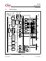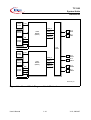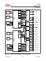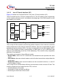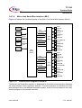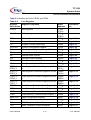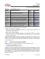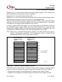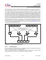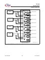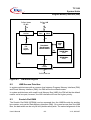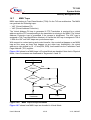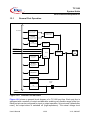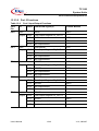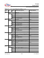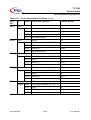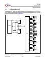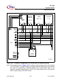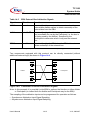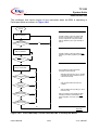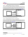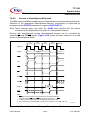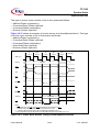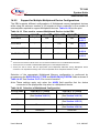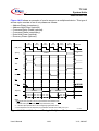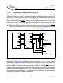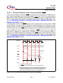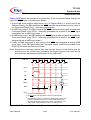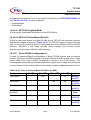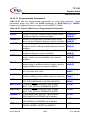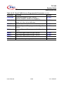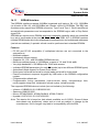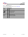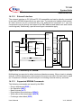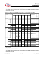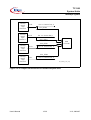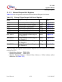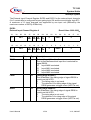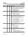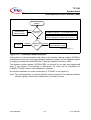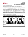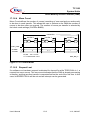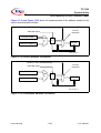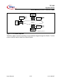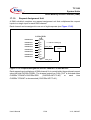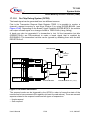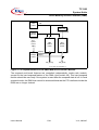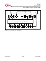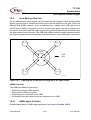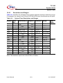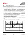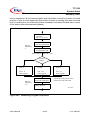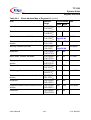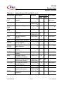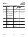
1
User’s Manual, V1.0, July 2004 TC1100 System Units 32-Bit Single-Chip Microcontroller Microcontrollers N e v e r s t o p t h i n k i n g . Edition 2004-07 Published by Infineon Technologies AG, St.-Martin-Strasse 53, D-81541 München, Germany © Infineon Technologies AG 2004. All Rights Reserved. Attention please! The information herein is given to describe certain components and shall not be considered as warranted characteristics. Terms of delivery and rights to technical change reserved. We hereby disclaim any and all warranties, including but not limited to warranties of non-infringement, regarding circuits, descriptions and charts stated herein. Infineon Technologies is an approved CECC manufacturer. Information For further information on technology, delivery terms and conditions and prices please contact your nearest Infineon Technologies Office in Germany or our Infineon Technologies Representatives worldwide. Warnings Due to technical requirements components may contain dangerous substances. For information on the types in question please contact your nearest Infineon Technologies Office. Infineon Technologies Components may only be used in life-support devices or systems with the express written approval of Infineon Technologies, if a failure of such components can reasonably be expected to cause the failure of that life-support device or system, or to affect the safety or effectiveness of that device or system. Life support devices or systems are intended to be implanted in the human body, or to support and/or maintain and sustain and/or protect human life. If they fail, it is reasonable to assume that the health of the user or other persons may be endangered. User’s Manual, V1.0, July 2004 TC1100 System Units 32-Bit Single-Chip Microcontroller Microcontrollers N e v e r s t o p t h i n k i n g . We Listen to Your Comments Any information within this document that you feel is wrong, unclear or missing? Your feedback will help us to continuously improve the quality of this document. Please send your proposal (including a reference to this document) to: [email protected] TC1100 System Units Table of Contents Page 1 1.1 1.1.1 1.1.2 1.1.3 1.1.4 1.1.5 1.2 1.3 1.4 1.4.1 1.4.1.1 1.4.1.2 1.4.1.3 1.4.1.4 1.4.2 1.4.3 1.5 Introduction . . . . . . . . . . . . . . . . . . . . . . . . . . . . . . . . . . . . . . . . . . . . . . 1-1 About this Document . . . . . . . . . . . . . . . . . . . . . . . . . . . . . . . . . . . . . . . . 1-1 Related Documentations . . . . . . . . . . . . . . . . . . . . . . . . . . . . . . . . . . . 1-1 Textual Conventions . . . . . . . . . . . . . . . . . . . . . . . . . . . . . . . . . . . . . . 1-1 Reserved, Undefined, and Unimplemented Terminology . . . . . . . . . . 1-3 Register Access Modes . . . . . . . . . . . . . . . . . . . . . . . . . . . . . . . . . . . . 1-3 Acronyms . . . . . . . . . . . . . . . . . . . . . . . . . . . . . . . . . . . . . . . . . . . . . . . 1-4 System Architecture Features of the TC1100 . . . . . . . . . . . . . . . . . . . . . 1-7 Block Diagram . . . . . . . . . . . . . . . . . . . . . . . . . . . . . . . . . . . . . . . . . . . . 1-10 On-Chip Peripheral Units of the TC1100 . . . . . . . . . . . . . . . . . . . . . . . 1-11 Serial Interfaces . . . . . . . . . . . . . . . . . . . . . . . . . . . . . . . . . . . . . . . . . 1-12 Asynchronous/Synchronous Serial Interface (ASC) . . . . . . . . . . . 1-12 High-Speed Synchronous Serial Interface (SSC) . . . . . . . . . . . . . 1-15 Inter IC Serial Interface (IIC) . . . . . . . . . . . . . . . . . . . . . . . . . . . . . 1-17 Micro Link Serial Bus Interface (MLI) . . . . . . . . . . . . . . . . . . . . . . . 1-18 General Purpose Timer Unit . . . . . . . . . . . . . . . . . . . . . . . . . . . . . . . 1-20 Capture/Compare Unit 6 (CCU6) . . . . . . . . . . . . . . . . . . . . . . . . . . . . 1-22 Pin Definitions and Functions . . . . . . . . . . . . . . . . . . . . . . . . . . . . . . . . 1-24 2 2.1 2.1.1 2.1.2 2.1.3 2.1.4 2.2 2.2.1 2.2.2 2.3 2.3.1 2.4 2.5 2.6 2.7 2.8 2.8.1 2.8.2 2.8.2.1 2.8.2.2 2.8.2.3 2.8.3 2.8.3.1 2.8.3.2 TC1100 Processor Architecture . . . . . . . . . . . . . . . . . . . . . . . . . . . . . . 2-1 Programming Model . . . . . . . . . . . . . . . . . . . . . . . . . . . . . . . . . . . . . . . . 2-2 Architectural Registers . . . . . . . . . . . . . . . . . . . . . . . . . . . . . . . . . . . . . 2-2 Data Types . . . . . . . . . . . . . . . . . . . . . . . . . . . . . . . . . . . . . . . . . . . . . 2-3 Memory Model . . . . . . . . . . . . . . . . . . . . . . . . . . . . . . . . . . . . . . . . . . . 2-3 Addressing Modes . . . . . . . . . . . . . . . . . . . . . . . . . . . . . . . . . . . . . . . . 2-4 Tasks and Contexts . . . . . . . . . . . . . . . . . . . . . . . . . . . . . . . . . . . . . . . . . 2-5 Context Save Area (CSA) . . . . . . . . . . . . . . . . . . . . . . . . . . . . . . . . . . 2-6 Fast Context Switching . . . . . . . . . . . . . . . . . . . . . . . . . . . . . . . . . . . . 2-7 Interrupt System . . . . . . . . . . . . . . . . . . . . . . . . . . . . . . . . . . . . . . . . . . . 2-7 Interrupt Priority . . . . . . . . . . . . . . . . . . . . . . . . . . . . . . . . . . . . . . . . . . 2-7 Trap System . . . . . . . . . . . . . . . . . . . . . . . . . . . . . . . . . . . . . . . . . . . . . . 2-8 Memory Management Unit (MMU) . . . . . . . . . . . . . . . . . . . . . . . . . . . . . 2-8 Protection System . . . . . . . . . . . . . . . . . . . . . . . . . . . . . . . . . . . . . . . . . . 2-9 Debug System . . . . . . . . . . . . . . . . . . . . . . . . . . . . . . . . . . . . . . . . . . . . 2-10 Processor Registers . . . . . . . . . . . . . . . . . . . . . . . . . . . . . . . . . . . . . . . 2-10 General Purpose Registers (GPRs) . . . . . . . . . . . . . . . . . . . . . . . . . 2-12 Program State Information Registers . . . . . . . . . . . . . . . . . . . . . . . . 2-14 Program Counter (PC) . . . . . . . . . . . . . . . . . . . . . . . . . . . . . . . . . . 2-14 Program Status Word (PSW) . . . . . . . . . . . . . . . . . . . . . . . . . . . . . 2-15 Previous Context Information Register (PCXI) . . . . . . . . . . . . . . . 2-19 Context Management Registers . . . . . . . . . . . . . . . . . . . . . . . . . . . . 2-21 Free Context List Head Pointer (FCX) . . . . . . . . . . . . . . . . . . . . . . 2-21 Previous Context Pointer (PCX) . . . . . . . . . . . . . . . . . . . . . . . . . . 2-22 User’s Manual I-1 V1.0, 2004-07 TC1100 System Units Table of Contents Page 2.8.4 Free Context List Limit Pointer (LCX) . . . . . . . . . . . . . . . . . . . . . . . . 2.8.5 Stack Management . . . . . . . . . . . . . . . . . . . . . . . . . . . . . . . . . . . . . . 2.8.5.1 Interrupt Stack Pointer (ISP) . . . . . . . . . . . . . . . . . . . . . . . . . . . . . 2.8.6 Interrupt and Trap Control . . . . . . . . . . . . . . . . . . . . . . . . . . . . . . . . . 2.8.6.1 Interrupt Control Register (ICR) . . . . . . . . . . . . . . . . . . . . . . . . . . . 2.8.6.2 Interrupt Vector Table Pointer (BIV) . . . . . . . . . . . . . . . . . . . . . . . 2.8.6.3 Trap Vector Table Pointer (BTV) . . . . . . . . . . . . . . . . . . . . . . . . . . 2.8.7 System Control Register . . . . . . . . . . . . . . . . . . . . . . . . . . . . . . . . . . 2.8.8 Memory Management Unit (MMU) Registers . . . . . . . . . . . . . . . . . . 2.8.9 Memory Protection Registers . . . . . . . . . . . . . . . . . . . . . . . . . . . . . . 2.8.10 Debug Registers . . . . . . . . . . . . . . . . . . . . . . . . . . . . . . . . . . . . . . . . 2.9 Instruction Set Overview . . . . . . . . . . . . . . . . . . . . . . . . . . . . . . . . . . . . 2.9.1 PSW Status Flags and Arithmetic . . . . . . . . . . . . . . . . . . . . . . . . . . . 2.9.2 Integer Arithmetic . . . . . . . . . . . . . . . . . . . . . . . . . . . . . . . . . . . . . . . . 2.9.2.1 Move . . . . . . . . . . . . . . . . . . . . . . . . . . . . . . . . . . . . . . . . . . . . . . . 2.9.2.2 Addition and Subtraction . . . . . . . . . . . . . . . . . . . . . . . . . . . . . . . . 2.9.2.3 Multiply and Multiply-Add . . . . . . . . . . . . . . . . . . . . . . . . . . . . . . . . 2.9.2.4 Division . . . . . . . . . . . . . . . . . . . . . . . . . . . . . . . . . . . . . . . . . . . . . 2.9.2.5 Absolute Value, Absolute Difference . . . . . . . . . . . . . . . . . . . . . . . 2.9.2.6 Min, Max, Saturate . . . . . . . . . . . . . . . . . . . . . . . . . . . . . . . . . . . . . 2.9.2.7 Conditional Arithmetic Instructions . . . . . . . . . . . . . . . . . . . . . . . . 2.9.2.8 Logic Operations . . . . . . . . . . . . . . . . . . . . . . . . . . . . . . . . . . . . . . 2.9.2.9 Count Leading Zeroes, Ones, and Signs . . . . . . . . . . . . . . . . . . . . 2.9.2.10 Shift . . . . . . . . . . . . . . . . . . . . . . . . . . . . . . . . . . . . . . . . . . . . . . . . 2.9.2.11 Bit Field Extract and Insert . . . . . . . . . . . . . . . . . . . . . . . . . . . . . . . 2.9.3 Packed Arithmetic . . . . . . . . . . . . . . . . . . . . . . . . . . . . . . . . . . . . . . . 2.9.4 DSP Arithmetic . . . . . . . . . . . . . . . . . . . . . . . . . . . . . . . . . . . . . . . . . 2.9.4.1 Scaling . . . . . . . . . . . . . . . . . . . . . . . . . . . . . . . . . . . . . . . . . . . . . . 2.9.4.2 Special Case = –1 * –1 => +1 . . . . . . . . . . . . . . . . . . . . . . . . . . . . 2.9.4.3 Guard Bits . . . . . . . . . . . . . . . . . . . . . . . . . . . . . . . . . . . . . . . . . . . 2.9.4.4 Rounding . . . . . . . . . . . . . . . . . . . . . . . . . . . . . . . . . . . . . . . . . . . . 2.9.4.5 Overflow and Saturation . . . . . . . . . . . . . . . . . . . . . . . . . . . . . . . . 2.9.4.6 Sticky Advance Overflow and Block Scaling in FFT . . . . . . . . . . . 2.9.4.7 Multiply and “MAC” . . . . . . . . . . . . . . . . . . . . . . . . . . . . . . . . . . . . 2.9.4.8 Packed Multiply and Packed “MAC” . . . . . . . . . . . . . . . . . . . . . . . 2.9.5 Compare Instructions . . . . . . . . . . . . . . . . . . . . . . . . . . . . . . . . . . . . . 2.9.6 Bit Operations . . . . . . . . . . . . . . . . . . . . . . . . . . . . . . . . . . . . . . . . . . 2.9.7 Address Arithmetic . . . . . . . . . . . . . . . . . . . . . . . . . . . . . . . . . . . . . . . 2.9.8 Address Comparison . . . . . . . . . . . . . . . . . . . . . . . . . . . . . . . . . . . . . 2.9.9 Branch Instructions . . . . . . . . . . . . . . . . . . . . . . . . . . . . . . . . . . . . . . 2.9.9.1 Unconditional Branch . . . . . . . . . . . . . . . . . . . . . . . . . . . . . . . . . . . 2.9.9.2 Conditional Branch . . . . . . . . . . . . . . . . . . . . . . . . . . . . . . . . . . . . User’s Manual I-2 2-23 2-23 2-23 2-24 2-24 2-26 2-27 2-28 2-28 2-29 2-29 2-36 2-36 2-37 2-37 2-37 2-38 2-38 2-39 2-39 2-39 2-40 2-40 2-41 2-41 2-43 2-45 2-45 2-45 2-46 2-46 2-46 2-46 2-46 2-47 2-47 2-50 2-52 2-53 2-54 2-54 2-55 V1.0, 2004-07 TC1100 System Units Table of Contents Page 2.9.9.3 Loop Instructions . . . . . . . . . . . . . . . . . . . . . . . . . . . . . . . . . . . . . . 2.9.10 Load and Store Instructions . . . . . . . . . . . . . . . . . . . . . . . . . . . . . . . . 2.9.10.1 Load/Store Basic Data Types . . . . . . . . . . . . . . . . . . . . . . . . . . . . 2.9.10.2 Load Bit . . . . . . . . . . . . . . . . . . . . . . . . . . . . . . . . . . . . . . . . . . . . . 2.9.10.3 Store Bit and Bit Field . . . . . . . . . . . . . . . . . . . . . . . . . . . . . . . . . . 2.9.11 Context Related Instructions . . . . . . . . . . . . . . . . . . . . . . . . . . . . . . . 2.9.11.1 Context Saving and Restoring . . . . . . . . . . . . . . . . . . . . . . . . . . . . 2.9.11.2 Context Loading and Storing . . . . . . . . . . . . . . . . . . . . . . . . . . . . . 2.9.12 System Instructions . . . . . . . . . . . . . . . . . . . . . . . . . . . . . . . . . . . . . . 2.9.12.1 System Call . . . . . . . . . . . . . . . . . . . . . . . . . . . . . . . . . . . . . . . . . . 2.9.12.2 Synchronization Primitives . . . . . . . . . . . . . . . . . . . . . . . . . . . . . . . 2.9.12.3 Access to the Core Special Function Registers (CSFRs) . . . . . . . 2.9.12.4 Enabling/Disabling the Interrupt System . . . . . . . . . . . . . . . . . . . . 2.9.12.5 RET and RFE . . . . . . . . . . . . . . . . . . . . . . . . . . . . . . . . . . . . . . . . 2.9.12.6 Trap Instructions . . . . . . . . . . . . . . . . . . . . . . . . . . . . . . . . . . . . . . 2.9.12.7 No-operation (NOP) . . . . . . . . . . . . . . . . . . . . . . . . . . . . . . . . . . . . 2.9.13 16-bit Instructions . . . . . . . . . . . . . . . . . . . . . . . . . . . . . . . . . . . . . . . 2.10 FPU . . . . . . . . . . . . . . . . . . . . . . . . . . . . . . . . . . . . . . . . . . . . . . . . . . . . 2.10.1 Data Format . . . . . . . . . . . . . . . . . . . . . . . . . . . . . . . . . . . . . . . . . . . . 2.10.2 Denormal Numbers . . . . . . . . . . . . . . . . . . . . . . . . . . . . . . . . . . . . . . 2.10.3 Floating Point Registers . . . . . . . . . . . . . . . . . . . . . . . . . . . . . . . . . . . 2.10.4 Extended Precision . . . . . . . . . . . . . . . . . . . . . . . . . . . . . . . . . . . . . . 2.10.5 Exception Conditions . . . . . . . . . . . . . . . . . . . . . . . . . . . . . . . . . . . . . 2.10.6 Rounding . . . . . . . . . . . . . . . . . . . . . . . . . . . . . . . . . . . . . . . . . . . . . . 2.10.7 FPU Instructions . . . . . . . . . . . . . . . . . . . . . . . . . . . . . . . . . . . . . . . . 2.10.7.1 Arithmetic Operations . . . . . . . . . . . . . . . . . . . . . . . . . . . . . . . . . . 2.10.7.2 Non-Arithmetic Operations . . . . . . . . . . . . . . . . . . . . . . . . . . . . . . 2.10.7.3 Conversion Operations . . . . . . . . . . . . . . . . . . . . . . . . . . . . . . . . . 2.10.8 Exception Handling . . . . . . . . . . . . . . . . . . . . . . . . . . . . . . . . . . . . . . 2.10.8.1 Invalid Operation . . . . . . . . . . . . . . . . . . . . . . . . . . . . . . . . . . . . . . 2.10.8.2 Divide by Zero . . . . . . . . . . . . . . . . . . . . . . . . . . . . . . . . . . . . . . . . 2.10.8.3 Overflow . . . . . . . . . . . . . . . . . . . . . . . . . . . . . . . . . . . . . . . . . . . . . 2.10.8.4 Underflow . . . . . . . . . . . . . . . . . . . . . . . . . . . . . . . . . . . . . . . . . . . . 2.10.8.5 Inexact . . . . . . . . . . . . . . . . . . . . . . . . . . . . . . . . . . . . . . . . . . . . . . 2.10.9 Cycle Counts by Opcode . . . . . . . . . . . . . . . . . . . . . . . . . . . . . . . . . . 2.11 CPU Slave Interface (CPS) . . . . . . . . . . . . . . . . . . . . . . . . . . . . . . . . . . 2.11.1 Feature Summary . . . . . . . . . . . . . . . . . . . . . . . . . . . . . . . . . . . . . . . 2.11.2 SFRs of the CPU Slave Interface (CPS) . . . . . . . . . . . . . . . . . . . . . . 2.12 CPU Register Address Ranges . . . . . . . . . . . . . . . . . . . . . . . . . . . . . . . 3 3.1 3.2 2-56 2-57 2-57 2-58 2-59 2-60 2-60 2-60 2-61 2-61 2-61 2-62 2-62 2-63 2-63 2-63 2-63 2-64 2-64 2-65 2-65 2-65 2-65 2-66 2-67 2-67 2-69 2-69 2-71 2-71 2-72 2-72 2-72 2-73 2-73 2-75 2-75 2-75 2-78 Clock System . . . . . . . . . . . . . . . . . . . . . . . . . . . . . . . . . . . . . . . . . . . . . 3-1 Clock Generation Unit . . . . . . . . . . . . . . . . . . . . . . . . . . . . . . . . . . . . . . . 3-3 Clock Registers . . . . . . . . . . . . . . . . . . . . . . . . . . . . . . . . . . . . . . . . . . . . 3-5 User’s Manual I-3 V1.0, 2004-07 TC1100 System Units Table of Contents Page 3.2.1 3.2.2 3.2.2.1 3.2.2.2 3.2.3 3.2.3.1 3.2.3.2 3.2.4 3.2.5 3.2.6 3.3 3.3.1 3.3.1.1 3.3.1.2 3.3.1.3 Main Oscillator Circuit . . . . . . . . . . . . . . . . . . . . . . . . . . . . . . . . . . . . . 3-5 PLL Module . . . . . . . . . . . . . . . . . . . . . . . . . . . . . . . . . . . . . . . . . . . . . 3-9 PLL Functional Description . . . . . . . . . . . . . . . . . . . . . . . . . . . . . . . 3-9 PLL Clock Control and Status Register . . . . . . . . . . . . . . . . . . . . . 3-12 Clock Source Control . . . . . . . . . . . . . . . . . . . . . . . . . . . . . . . . . . . . . 3-15 Setting up the PLL after Reset . . . . . . . . . . . . . . . . . . . . . . . . . . . . 3-16 Switching PLL Parameters . . . . . . . . . . . . . . . . . . . . . . . . . . . . . . 3-17 Power-on Startup Operation . . . . . . . . . . . . . . . . . . . . . . . . . . . . . . . 3-17 Loss-of-Lock Operation . . . . . . . . . . . . . . . . . . . . . . . . . . . . . . . . . . . 3-18 Loss-of-Lock Recovery . . . . . . . . . . . . . . . . . . . . . . . . . . . . . . . . . . . 3-19 Module Power Management and Clock Gating . . . . . . . . . . . . . . . . . . . 3-19 Module Clock Generation . . . . . . . . . . . . . . . . . . . . . . . . . . . . . . . . . 3-20 Clock Control Registers . . . . . . . . . . . . . . . . . . . . . . . . . . . . . . . . 3-21 Fractional Divider . . . . . . . . . . . . . . . . . . . . . . . . . . . . . . . . . . . . . . 3-26 Module Clock Generation Implementations . . . . . . . . . . . . . . . . . . 3-36 4 4.1 4.2 4.3 4.4 4.5 4.6 4.7 4.8 4.8.1 System Control Unit . . . . . . . . . . . . . . . . . . . . . . . . . . . . . . . . . . . . . . . 4-1 Overview . . . . . . . . . . . . . . . . . . . . . . . . . . . . . . . . . . . . . . . . . . . . . . . . . 4-1 Parity Error Control . . . . . . . . . . . . . . . . . . . . . . . . . . . . . . . . . . . . . . . . . 4-1 Faulty SRAM Fuse Box . . . . . . . . . . . . . . . . . . . . . . . . . . . . . . . . . . . . . 4-5 CSCOMB (CSovl/CSglb) Control . . . . . . . . . . . . . . . . . . . . . . . . . . . . . . . 4-7 EBU Pull-Up Control . . . . . . . . . . . . . . . . . . . . . . . . . . . . . . . . . . . . . . . . 4-7 DMA Request Signal Selection . . . . . . . . . . . . . . . . . . . . . . . . . . . . . . . . 4-7 Miscellaneous SCU Registers . . . . . . . . . . . . . . . . . . . . . . . . . . . . . . . . 4-11 SCU Registers and Address Map . . . . . . . . . . . . . . . . . . . . . . . . . . . . . 4-18 SCU Register Address Range . . . . . . . . . . . . . . . . . . . . . . . . . . . . . . 4-20 5 5.1 5.2 5.2.1 5.2.2 5.3 5.3.1 5.3.2 5.3.3 5.3.4 5.3.5 5.3.6 5.3.7 5.4 5.4.1 5.4.2 Reset and Boot Operation . . . . . . . . . . . . . . . . . . . . . . . . . . . . . . . . . . 5-1 Overview . . . . . . . . . . . . . . . . . . . . . . . . . . . . . . . . . . . . . . . . . . . . . . . . . 5-1 Reset Registers . . . . . . . . . . . . . . . . . . . . . . . . . . . . . . . . . . . . . . . . . . . . 5-2 Reset Status Register (RST_SR) . . . . . . . . . . . . . . . . . . . . . . . . . . . . 5-2 Reset Request Register (RST_REQ) . . . . . . . . . . . . . . . . . . . . . . . . . 5-4 Reset Operations . . . . . . . . . . . . . . . . . . . . . . . . . . . . . . . . . . . . . . . . . . . 5-6 Power-On Reset . . . . . . . . . . . . . . . . . . . . . . . . . . . . . . . . . . . . . . . . . 5-6 External Hard Reset . . . . . . . . . . . . . . . . . . . . . . . . . . . . . . . . . . . . . . 5-6 Soft Reset . . . . . . . . . . . . . . . . . . . . . . . . . . . . . . . . . . . . . . . . . . . . . . 5-7 Watchdog Timer Reset . . . . . . . . . . . . . . . . . . . . . . . . . . . . . . . . . . . . 5-7 Deep Sleep Wake-Up Reset . . . . . . . . . . . . . . . . . . . . . . . . . . . . . . . . 5-8 Debug System Reset . . . . . . . . . . . . . . . . . . . . . . . . . . . . . . . . . . . . . . 5-9 State of the TC1100 After Reset . . . . . . . . . . . . . . . . . . . . . . . . . . . . . 5-9 Booting Scheme . . . . . . . . . . . . . . . . . . . . . . . . . . . . . . . . . . . . . . . . . . 5-11 Boot Options . . . . . . . . . . . . . . . . . . . . . . . . . . . . . . . . . . . . . . . . . . . 5-11 Normal Boot Options . . . . . . . . . . . . . . . . . . . . . . . . . . . . . . . . . . . . 5-12 User’s Manual I-4 V1.0, 2004-07 TC1100 System Units Table of Contents Page 5.4.3 5.5 5.5.1 5.5.2 Debug Boot Options . . . . . . . . . . . . . . . . . . . . . . . . . . . . . . . . . . . . . Configuration Input Sampling . . . . . . . . . . . . . . . . . . . . . . . . . . . . . . . . Hardware Configuration Inputs . . . . . . . . . . . . . . . . . . . . . . . . . . . . . Software Option Select Inputs . . . . . . . . . . . . . . . . . . . . . . . . . . . . . . 6 6.1 6.2 6.2.1 6.2.2 6.3 6.3.1 6.3.2 6.3.2.1 6.3.2.2 6.3.2.3 6.3.3 6.3.3.1 6.3.3.2 6.3.3.3 6.3.3.4 6.3.3.5 6.3.4 Power Management . . . . . . . . . . . . . . . . . . . . . . . . . . . . . . . . . . . . . . . . 6-1 Power Management Overview . . . . . . . . . . . . . . . . . . . . . . . . . . . . . . . . . 6-1 Power Management Control Registers . . . . . . . . . . . . . . . . . . . . . . . . . . 6-3 Power Management Control Register PMG_CON . . . . . . . . . . . . . . . 6-3 Power Management Control and Status Register PMG_CSR . . . . . . . 6-5 Power Management Modes . . . . . . . . . . . . . . . . . . . . . . . . . . . . . . . . . . . 6-6 Idle Mode . . . . . . . . . . . . . . . . . . . . . . . . . . . . . . . . . . . . . . . . . . . . . . . 6-6 Sleep Mode . . . . . . . . . . . . . . . . . . . . . . . . . . . . . . . . . . . . . . . . . . . . . 6-6 Entering Sleep Mode . . . . . . . . . . . . . . . . . . . . . . . . . . . . . . . . . . . . 6-6 TC1100 State During Sleep Mode . . . . . . . . . . . . . . . . . . . . . . . . . . 6-7 Exiting Sleep Mode . . . . . . . . . . . . . . . . . . . . . . . . . . . . . . . . . . . . . 6-7 Deep Sleep Mode . . . . . . . . . . . . . . . . . . . . . . . . . . . . . . . . . . . . . . . . 6-7 Entering Deep Sleep Mode . . . . . . . . . . . . . . . . . . . . . . . . . . . . . . . 6-8 TC1100 State During Deep Sleep Mode . . . . . . . . . . . . . . . . . . . . . 6-8 Exiting Deep Sleep Mode . . . . . . . . . . . . . . . . . . . . . . . . . . . . . . . . 6-8 Exiting Deep Sleep Mode With a Power-On Reset Signal . . . . . . . 6-9 Exiting Deep Sleep Mode With a NMI Signal . . . . . . . . . . . . . . . . . 6-9 Summary of TC1100 Power Management States . . . . . . . . . . . . . . . 6-10 7 Memory Map of On-Chip Local Memories . . . . . . . . . . . . . . . . . . . . . . 7-1 8 8.1 8.2 8.3 8.4 8.4.1 8.4.2 8.4.3 8.4.4 8.4.5 8.5 Program Memory Interface (PMI) . . . . . . . . . . . . . . . . . . . . . . . . . . . . Feature Summary and Block Diagram . . . . . . . . . . . . . . . . . . . . . . . . . . . LMB Access Priorities . . . . . . . . . . . . . . . . . . . . . . . . . . . . . . . . . . . . . . . Scratch-Pad RAM . . . . . . . . . . . . . . . . . . . . . . . . . . . . . . . . . . . . . . . . . . Instruction Cache . . . . . . . . . . . . . . . . . . . . . . . . . . . . . . . . . . . . . . . . . . . Cache Organization . . . . . . . . . . . . . . . . . . . . . . . . . . . . . . . . . . . . . . . Cache Bypass Control . . . . . . . . . . . . . . . . . . . . . . . . . . . . . . . . . . . . . Refill Sequence for Cache . . . . . . . . . . . . . . . . . . . . . . . . . . . . . . . . . . Instruction Streaming . . . . . . . . . . . . . . . . . . . . . . . . . . . . . . . . . . . . . . Cache Coherency, Cache Invalidation . . . . . . . . . . . . . . . . . . . . . . . . PMI Registers . . . . . . . . . . . . . . . . . . . . . . . . . . . . . . . . . . . . . . . . . . . . . 8-1 8-1 8-2 8-2 8-3 8-3 8-3 8-4 8-4 8-4 8-5 9 9.1 9.2 9.3 9.3.1 9.3.2 Data Memory Interface (DMI) . . . . . . . . . . . . . . . . . . . . . . . . . . . . . . . . Feature Summary and Block Diagram . . . . . . . . . . . . . . . . . . . . . . . . . . . LMB Access Priorities . . . . . . . . . . . . . . . . . . . . . . . . . . . . . . . . . . . . . . . DMI Trap Generation . . . . . . . . . . . . . . . . . . . . . . . . . . . . . . . . . . . . . . . . LMB Bus Error . . . . . . . . . . . . . . . . . . . . . . . . . . . . . . . . . . . . . . . . . . . Range Error . . . . . . . . . . . . . . . . . . . . . . . . . . . . . . . . . . . . . . . . . . . . . 9-1 9-1 9-2 9-2 9-3 9-3 User’s Manual I-5 5-13 5-14 5-14 5-14 V1.0, 2004-07 TC1100 System Units Table of Contents Page 9.3.3 9.3.4 9.4 DMI Register Access Error . . . . . . . . . . . . . . . . . . . . . . . . . . . . . . . . . 9-3 Cache Management Error . . . . . . . . . . . . . . . . . . . . . . . . . . . . . . . . . . 9-4 DMI Registers . . . . . . . . . . . . . . . . . . . . . . . . . . . . . . . . . . . . . . . . . . . . . 9-4 10 10.1 10.2 10.2.1 10.3 10.3.1 10.4 10.4.1 10.4.2 10.4.3 10.5 10.5.1 10.5.2 10.6 10.7 10.8 10.8.1 10.8.2 10.8.3 10.8.4 10.9 10.9.1 10.9.2 10.9.3 10.9.4 10.9.5 10.9.6 10.9.7 Memory Management Unit . . . . . . . . . . . . . . . . . . . . . . . . . . . . . . . . . 10-1 Address Spaces . . . . . . . . . . . . . . . . . . . . . . . . . . . . . . . . . . . . . . . . . . . 10-3 Address Translation . . . . . . . . . . . . . . . . . . . . . . . . . . . . . . . . . . . . . . . . 10-4 Address Translation for Context Pointers . . . . . . . . . . . . . . . . . . . . . 10-4 Translation Lookaside Buffers (TLBs) . . . . . . . . . . . . . . . . . . . . . . . . . . 10-5 TLB Table Entry Contents . . . . . . . . . . . . . . . . . . . . . . . . . . . . . . . . . 10-5 Cacheability . . . . . . . . . . . . . . . . . . . . . . . . . . . . . . . . . . . . . . . . . . . . . . 10-7 Cacheability for Direct Translation . . . . . . . . . . . . . . . . . . . . . . . . . . . 10-7 Cacheability for PTE based Translation . . . . . . . . . . . . . . . . . . . . . . 10-7 Complete Description . . . . . . . . . . . . . . . . . . . . . . . . . . . . . . . . . . . . 10-7 Protection . . . . . . . . . . . . . . . . . . . . . . . . . . . . . . . . . . . . . . . . . . . . . . . . 10-9 Protection for Direct Translation . . . . . . . . . . . . . . . . . . . . . . . . . . . . 10-9 Protection for PTE Translation . . . . . . . . . . . . . . . . . . . . . . . . . . . . . . 10-9 Multiple Address Spaces . . . . . . . . . . . . . . . . . . . . . . . . . . . . . . . . . . . . 10-9 MMU Traps . . . . . . . . . . . . . . . . . . . . . . . . . . . . . . . . . . . . . . . . . . . . . 10-10 MMU Instructions . . . . . . . . . . . . . . . . . . . . . . . . . . . . . . . . . . . . . . . . . 10-12 TLBMAP (TLB Map) . . . . . . . . . . . . . . . . . . . . . . . . . . . . . . . . . . . . 10-12 TLBDEMAP (TLB Demap) . . . . . . . . . . . . . . . . . . . . . . . . . . . . . . . . 10-12 TLBFLUSH (TLB Flush) . . . . . . . . . . . . . . . . . . . . . . . . . . . . . . . . . . 10-12 TLBPROBE (TLB Probe) . . . . . . . . . . . . . . . . . . . . . . . . . . . . . . . . . 10-13 MMU Registers . . . . . . . . . . . . . . . . . . . . . . . . . . . . . . . . . . . . . . . . . . 10-13 Configuration Register . . . . . . . . . . . . . . . . . . . . . . . . . . . . . . . . . . . 10-14 Address Space Identifier Register . . . . . . . . . . . . . . . . . . . . . . . . . . 10-16 Translation Virtual Address Register . . . . . . . . . . . . . . . . . . . . . . . . 10-16 Translation Physical Address Register . . . . . . . . . . . . . . . . . . . . . . 10-17 Translation Page Index Register . . . . . . . . . . . . . . . . . . . . . . . . . . . 10-19 Translation Fault Page Address Register . . . . . . . . . . . . . . . . . . . . 10-19 MMU Register Address Ranges . . . . . . . . . . . . . . . . . . . . . . . . . . . 10-20 11 11.1 11.2 11.3 11.3.1 11.3.2 11.4 11.5 11.5.1 11.5.2 Data Memory Unit (DMU) . . . . . . . . . . . . . . . . . . . . . . . . . . . . . . . . . . 11-1 SRAM Redundancy Control . . . . . . . . . . . . . . . . . . . . . . . . . . . . . . . . . . 11-2 DMU SRAM Redundancy Register Programming . . . . . . . . . . . . . . . . . 11-2 CPU Configuration Register Programming . . . . . . . . . . . . . . . . . . . . . . 11-4 Functional Description . . . . . . . . . . . . . . . . . . . . . . . . . . . . . . . . . . . . 11-4 Reading CSCADOUT . . . . . . . . . . . . . . . . . . . . . . . . . . . . . . . . . . . . 11-5 Soft Error Detection . . . . . . . . . . . . . . . . . . . . . . . . . . . . . . . . . . . . . . . . 11-6 DMU Registers . . . . . . . . . . . . . . . . . . . . . . . . . . . . . . . . . . . . . . . . . . . 11-7 DMU SRAM Redundancy Registers . . . . . . . . . . . . . . . . . . . . . . . . 11-10 CPU SRAM Configuration Registers . . . . . . . . . . . . . . . . . . . . . . . . 11-10 User’s Manual I-6 V1.0, 2004-07 TC1100 System Units Table of Contents Page 11.5.3 11.5.4 Soft Error Detection Register . . . . . . . . . . . . . . . . . . . . . . . . . . . . . . 11-13 DMU Register Address Ranges . . . . . . . . . . . . . . . . . . . . . . . . . . . . 11-14 12 12.1 12.2 12.2.1 12.2.2 12.2.3 12.3 12.4 12.4.1 12.4.2 12.5 Memory Protection System . . . . . . . . . . . . . . . . . . . . . . . . . . . . . . . . 12-1 Memory Protection Overview . . . . . . . . . . . . . . . . . . . . . . . . . . . . . . . . . 12-1 Memory Protection Registers . . . . . . . . . . . . . . . . . . . . . . . . . . . . . . . . 12-3 PSW Protection Fields . . . . . . . . . . . . . . . . . . . . . . . . . . . . . . . . . . . . 12-6 Data Memory Protection Register . . . . . . . . . . . . . . . . . . . . . . . . . . . 12-6 Code Memory Protection Register . . . . . . . . . . . . . . . . . . . . . . . . . . 12-12 Sample Protection Register Set . . . . . . . . . . . . . . . . . . . . . . . . . . . . . . 12-16 Memory Access Checking . . . . . . . . . . . . . . . . . . . . . . . . . . . . . . . . . . 12-17 Permitted versus Valid Accesses . . . . . . . . . . . . . . . . . . . . . . . . . . 12-17 Crossing Protection Boundaries . . . . . . . . . . . . . . . . . . . . . . . . . . . 12-18 Memory Protection Register Address Ranges . . . . . . . . . . . . . . . . . . . 12-19 13 13.1 13.2 13.2.1 13.2.2 13.2.3 13.2.4 13.2.5 13.2.6 13.2.7 13.3 13.3.1 13.3.1.1 13.3.1.2 13.3.2 13.3.2.1 13.3.2.2 13.3.3 13.3.3.1 13.3.3.2 13.3.4 13.3.4.1 13.3.4.2 13.3.5 13.3.5.1 13.3.5.2 13.4 GPIO Ports and Peripheral I/O . . . . . . . . . . . . . . . . . . . . . . . . . . . . . General Port Operation . . . . . . . . . . . . . . . . . . . . . . . . . . . . . . . . . . . . Port Kernel Registers . . . . . . . . . . . . . . . . . . . . . . . . . . . . . . . . . . . . . Port Output Register . . . . . . . . . . . . . . . . . . . . . . . . . . . . . . . . . . . . Port Input Register . . . . . . . . . . . . . . . . . . . . . . . . . . . . . . . . . . . . . . Direction Register . . . . . . . . . . . . . . . . . . . . . . . . . . . . . . . . . . . . . . Open Drain Control Register . . . . . . . . . . . . . . . . . . . . . . . . . . . . . . Pull-Up/Pull-Down Device Register . . . . . . . . . . . . . . . . . . . . . . . . . Alternate Input Functions . . . . . . . . . . . . . . . . . . . . . . . . . . . . . . . . . Alternate Output Functions . . . . . . . . . . . . . . . . . . . . . . . . . . . . . . . Port Implementation . . . . . . . . . . . . . . . . . . . . . . . . . . . . . . . . . . . . . . . Port 0 . . . . . . . . . . . . . . . . . . . . . . . . . . . . . . . . . . . . . . . . . . . . . . . . Overview . . . . . . . . . . . . . . . . . . . . . . . . . . . . . . . . . . . . . . . . . . . Port 0 Functions . . . . . . . . . . . . . . . . . . . . . . . . . . . . . . . . . . . . . . Port 1 . . . . . . . . . . . . . . . . . . . . . . . . . . . . . . . . . . . . . . . . . . . . . . . . Overview . . . . . . . . . . . . . . . . . . . . . . . . . . . . . . . . . . . . . . . . . . . Port 1 Functions . . . . . . . . . . . . . . . . . . . . . . . . . . . . . . . . . . . . . . Port 2 . . . . . . . . . . . . . . . . . . . . . . . . . . . . . . . . . . . . . . . . . . . . . . . . Overview . . . . . . . . . . . . . . . . . . . . . . . . . . . . . . . . . . . . . . . . . . . Port 2 Functions . . . . . . . . . . . . . . . . . . . . . . . . . . . . . . . . . . . . . . Port 3 . . . . . . . . . . . . . . . . . . . . . . . . . . . . . . . . . . . . . . . . . . . . . . . . Overview . . . . . . . . . . . . . . . . . . . . . . . . . . . . . . . . . . . . . . . . . . . Port 3 Functions . . . . . . . . . . . . . . . . . . . . . . . . . . . . . . . . . . . . . . Port 4 . . . . . . . . . . . . . . . . . . . . . . . . . . . . . . . . . . . . . . . . . . . . . . . . Overview . . . . . . . . . . . . . . . . . . . . . . . . . . . . . . . . . . . . . . . . . . . Port 4 Functions . . . . . . . . . . . . . . . . . . . . . . . . . . . . . . . . . . . . . . Port Register Address Map . . . . . . . . . . . . . . . . . . . . . . . . . . . . . . . . . 14 External Bus Unit . . . . . . . . . . . . . . . . . . . . . . . . . . . . . . . . . . . . . . . . . 14-1 User’s Manual I-7 13-21 13-22 13-24 13-25 13-26 13-27 13-28 13-29 13-31 13-31 13-32 13-32 13-32 13-33 13-37 13-37 13-38 13-41 13-41 13-42 13-45 13-45 13-46 13-49 13-49 13-50 13-51 V1.0, 2004-07 TC1100 System Units Table of Contents 14.1 14.2 14.3 14.4 14.4.1 14.4.2 14.4.3 14.4.4 14.4.5 14.4.6 14.4.7 14.4.8 14.4.9 14.5 14.5.1 14.5.1.1 14.5.1.2 14.5.2 14.5.2.1 14.5.2.2 14.5.3 14.5.3.1 14.5.3.2 14.5.3.3 14.5.3.4 14.5.4 14.5.5 14.5.5.1 14.6 14.6.1 14.6.2 14.6.3 14.6.3.1 14.6.3.2 14.6.3.3 14.7 14.7.1 14.7.2 14.8 14.8.1 14.8.1.1 14.8.1.2 Page Overview . . . . . . . . . . . . . . . . . . . . . . . . . . . . . . . . . . . . . . . . . . . . . . . . 14-2 EBU Features . . . . . . . . . . . . . . . . . . . . . . . . . . . . . . . . . . . . . . . . . . . . 14-3 Basic EBU Operation . . . . . . . . . . . . . . . . . . . . . . . . . . . . . . . . . . . . . . . 14-4 EBU Signal Description . . . . . . . . . . . . . . . . . . . . . . . . . . . . . . . . . . . . . 14-7 Address Bus, A[23:0] . . . . . . . . . . . . . . . . . . . . . . . . . . . . . . . . . . . . . 14-8 Address/Data Bus, AD[31:0] . . . . . . . . . . . . . . . . . . . . . . . . . . . . . . . 14-8 Read/Write Strobes, RD and RD/WR . . . . . . . . . . . . . . . . . . . . . . . . 14-8 Address Latch Enable, ALE . . . . . . . . . . . . . . . . . . . . . . . . . . . . . . . . 14-9 Byte Control Signals, BCx . . . . . . . . . . . . . . . . . . . . . . . . . . . . . . . . . 14-9 Variable Wait State Control, WAIT . . . . . . . . . . . . . . . . . . . . . . . . . . 14-9 Chip Select Lines, CSx, CSGLB . . . . . . . . . . . . . . . . . . . . . . . . . . . 14-10 EBU Arbitration Signals, HOLD, HLDA and BREQ . . . . . . . . . . . . . 14-11 Emulation Support Signals, CSEMU and CSOVL . . . . . . . . . . . . . . 14-11 Arbitration . . . . . . . . . . . . . . . . . . . . . . . . . . . . . . . . . . . . . . . . . . . . . . 14-12 External Bus Modes . . . . . . . . . . . . . . . . . . . . . . . . . . . . . . . . . . . . . 14-12 Owner Mode . . . . . . . . . . . . . . . . . . . . . . . . . . . . . . . . . . . . . . . . 14-12 Hold Mode . . . . . . . . . . . . . . . . . . . . . . . . . . . . . . . . . . . . . . . . . . 14-12 Arbitration Signals . . . . . . . . . . . . . . . . . . . . . . . . . . . . . . . . . . . . . . 14-12 Synchronous Arbitration Input Signal Sampling . . . . . . . . . . . . . 14-14 Asynchronous Arbitration Input Signal Sampling . . . . . . . . . . . . . 14-14 Arbitration Modes . . . . . . . . . . . . . . . . . . . . . . . . . . . . . . . . . . . . . . . 14-14 No Bus . . . . . . . . . . . . . . . . . . . . . . . . . . . . . . . . . . . . . . . . . . . . . 14-14 EBU is Sole Master . . . . . . . . . . . . . . . . . . . . . . . . . . . . . . . . . . . 14-15 EBU is Arbiter . . . . . . . . . . . . . . . . . . . . . . . . . . . . . . . . . . . . . . . 14-15 EBU is Participant . . . . . . . . . . . . . . . . . . . . . . . . . . . . . . . . . . . . 14-19 Locking the External Bus . . . . . . . . . . . . . . . . . . . . . . . . . . . . . . . . . 14-22 EBU Reaction to an LMB Access to the External Bus . . . . . . . . . . . 14-23 Pending Access Time-out . . . . . . . . . . . . . . . . . . . . . . . . . . . . . . 14-24 EBU Start Up . . . . . . . . . . . . . . . . . . . . . . . . . . . . . . . . . . . . . . . . . . . . 14-25 Disabled . . . . . . . . . . . . . . . . . . . . . . . . . . . . . . . . . . . . . . . . . . . . . . 14-25 Emulation Mode . . . . . . . . . . . . . . . . . . . . . . . . . . . . . . . . . . . . . . . . 14-25 Boot Operation . . . . . . . . . . . . . . . . . . . . . . . . . . . . . . . . . . . . . . . . . 14-25 Boot Memory Type . . . . . . . . . . . . . . . . . . . . . . . . . . . . . . . . . . . 14-26 Boot Process . . . . . . . . . . . . . . . . . . . . . . . . . . . . . . . . . . . . . . . . 14-26 Boot Configuration Value . . . . . . . . . . . . . . . . . . . . . . . . . . . . . . . 14-28 Emulation Support . . . . . . . . . . . . . . . . . . . . . . . . . . . . . . . . . . . . . . . . 14-29 Emulation Boot . . . . . . . . . . . . . . . . . . . . . . . . . . . . . . . . . . . . . . . . 14-30 Overlay Memory . . . . . . . . . . . . . . . . . . . . . . . . . . . . . . . . . . . . . . . 14-30 EBU Operation . . . . . . . . . . . . . . . . . . . . . . . . . . . . . . . . . . . . . . . . . . . 14-32 EBU Address Regions . . . . . . . . . . . . . . . . . . . . . . . . . . . . . . . . . . . 14-32 Address Region Selection . . . . . . . . . . . . . . . . . . . . . . . . . . . . . . 14-33 Address Region Parameters . . . . . . . . . . . . . . . . . . . . . . . . . . . . 14-37 User’s Manual I-8 V1.0, 2004-07 TC1100 System Units Table of Contents Page 14.8.2 LMB Bus Width Translation . . . . . . . . . . . . . . . . . . . . . . . . . . . . . . . 14.8.3 External Bus Clock Generation . . . . . . . . . . . . . . . . . . . . . . . . . . . . 14.8.4 Address Alignment During Bus Accesses . . . . . . . . . . . . . . . . . . . . 14.8.5 Read/Modify/Write Accesses . . . . . . . . . . . . . . . . . . . . . . . . . . . . . . 14.8.6 Driver Turn-Around Wait States . . . . . . . . . . . . . . . . . . . . . . . . . . . . 14.8.7 Data Buffering . . . . . . . . . . . . . . . . . . . . . . . . . . . . . . . . . . . . . . . . . 14.8.8 Data Width of External Devices . . . . . . . . . . . . . . . . . . . . . . . . . . . . 14.8.9 Basic Access Timing . . . . . . . . . . . . . . . . . . . . . . . . . . . . . . . . . . . . 14.8.9.1 Standard Access Phases . . . . . . . . . . . . . . . . . . . . . . . . . . . . . . . 14.8.9.2 Multiplication Factor for Access Phase Length . . . . . . . . . . . . . . 14.9 Asynchronous Devices . . . . . . . . . . . . . . . . . . . . . . . . . . . . . . . . . . . . 14.9.1 Features . . . . . . . . . . . . . . . . . . . . . . . . . . . . . . . . . . . . . . . . . . . . . . 14.9.2 Signal List . . . . . . . . . . . . . . . . . . . . . . . . . . . . . . . . . . . . . . . . . . . . 14.9.3 Multiple Non-Multiplexed Device Configurations . . . . . . . . . . . . . . . 14.9.3.1 16-Bit Non-Multiplexed Device Configuration . . . . . . . . . . . . . . . 14.9.3.2 32-Bit Non-Multiplexed Device Configuration . . . . . . . . . . . . . . . 14.9.4 Access to Demultiplexed Devices . . . . . . . . . . . . . . . . . . . . . . . . . . 14.9.5 Support for Multiple Multiplexed Device Configurations . . . . . . . . . 14.9.5.1 16-bit Multiplexed Memory/Peripheral Configuration . . . . . . . . . . 14.9.5.2 32-bit Multiplexed Memory/Peripheral Configuration . . . . . . . . . . 14.9.5.3 WinCE 32-bit Multiplexed Memory/Peripheral Configuration . . . . 14.9.5.4 Twin 16-bit Multiplexed Device Configuration . . . . . . . . . . . . . . . 14.9.6 Access to Multiplexed Devices . . . . . . . . . . . . . . . . . . . . . . . . . . . . 14.9.7 Interfacing to Asynchronous Devices . . . . . . . . . . . . . . . . . . . . . . . 14.9.7.1 External Extension of the Command Phase WAIT . . . . . . . . . . . 14.9.8 Interfacing to Intel-style Devices . . . . . . . . . . . . . . . . . . . . . . . . . . . 14.10 Burst FLASH Devices Access . . . . . . . . . . . . . . . . . . . . . . . . . . . . . . . 14.10.1 Features . . . . . . . . . . . . . . . . . . . . . . . . . . . . . . . . . . . . . . . . . . . . . . 14.10.2 Signal List . . . . . . . . . . . . . . . . . . . . . . . . . . . . . . . . . . . . . . . . . . . . 14.10.3 Support for Two Burst FLASH Device Types . . . . . . . . . . . . . . . . . 14.10.4 BFCLKO Output . . . . . . . . . . . . . . . . . . . . . . . . . . . . . . . . . . . . . . . . 14.10.4.1 BFCLKO Ungated Mode . . . . . . . . . . . . . . . . . . . . . . . . . . . . . . . 14.10.4.2 BFCLKO Gated Mode (Default) . . . . . . . . . . . . . . . . . . . . . . . . . . 14.10.5 Burst FLASH Configurations . . . . . . . . . . . . . . . . . . . . . . . . . . . . . . 14.10.5.1 16-bit Multiplexed Burst FLASH Configuration . . . . . . . . . . . . . . 14.10.5.2 32-bit Multiplexed Burst FLASH Configuration . . . . . . . . . . . . . . 14.10.5.3 Twin 16-bit Multiplexed Burst FLASH Configuration . . . . . . . . . . 14.10.5.4 16-bit Non-Multiplexed Burst FLASH Configuration . . . . . . . . . . 14.10.5.5 32-bit Non-Multiplexed Burst FLASH Configuration . . . . . . . . . . 14.10.6 Standard Access Phases . . . . . . . . . . . . . . . . . . . . . . . . . . . . . . . . . 14.10.7 Burst Length Control . . . . . . . . . . . . . . . . . . . . . . . . . . . . . . . . . . . . 14.10.8 Control of ADV and BAA Delays During Burst FLASH Access . . . . 14-38 14-39 14-40 14-40 14-40 14-42 14-43 14-44 14-44 14-48 14-50 14-50 14-51 14-52 14-53 14-53 14-54 14-56 14-57 14-57 14-58 14-59 14-59 14-62 14-63 14-65 14-67 14-67 14-67 14-68 14-68 14-69 14-69 14-69 14-72 14-73 14-74 14-75 14-76 14-76 14-77 14-77 User’s Manual I-9 V1.0, 2004-07 TC1100 System Units Table of Contents Page 14.10.9 Burst FLASH Clock Feedback . . . . . . . . . . . . . . . . . . . . . . . . . . . . . 14-78 14.10.10 Cycle Definitions of Burst Mode Timing . . . . . . . . . . . . . . . . . . . . . . 14-79 14.10.11 External Cycle Control via the WAIT Input . . . . . . . . . . . . . . . . . . . 14-81 14.10.11.1 Wait for Page Load Mode (Intel) . . . . . . . . . . . . . . . . . . . . . . . . . 14-82 14.10.11.2 Terminate and Start New Burst Mode (AMD) . . . . . . . . . . . . . . . 14-83 14.10.12 Termination of a Burst Access . . . . . . . . . . . . . . . . . . . . . . . . . . . . . 14-84 14.10.13 Programmable Parameters . . . . . . . . . . . . . . . . . . . . . . . . . . . . . . . 14-85 14.11 SDRAM Interface . . . . . . . . . . . . . . . . . . . . . . . . . . . . . . . . . . . . . . . . . 14-87 14.11.1 SDRAM Signal List . . . . . . . . . . . . . . . . . . . . . . . . . . . . . . . . . . . . . 14-88 14.11.2 External Interface . . . . . . . . . . . . . . . . . . . . . . . . . . . . . . . . . . . . . . . 14-89 14.11.3 Supported SDRAM Commands . . . . . . . . . . . . . . . . . . . . . . . . . . . . 14-89 14.11.4 Power-Up Sequence . . . . . . . . . . . . . . . . . . . . . . . . . . . . . . . . . . . . 14-91 14.11.5 Initialization Sequence . . . . . . . . . . . . . . . . . . . . . . . . . . . . . . . . . . . 14-91 14.11.6 SDRAM Burst Accesses . . . . . . . . . . . . . . . . . . . . . . . . . . . . . . . . . 14-94 14.11.7 Multibanking Operation . . . . . . . . . . . . . . . . . . . . . . . . . . . . . . . . . . 14-97 14.11.7.1 Bank-Page Tag Structure . . . . . . . . . . . . . . . . . . . . . . . . . . . . . . 14-97 14.11.7.2 Bank Mask and Page Mask . . . . . . . . . . . . . . . . . . . . . . . . . . . . . 14-97 14.11.7.3 Decisions over Page_hit and Bank_hit . . . . . . . . . . . . . . . . . . . . 14-99 14.11.8 Banks Precharge . . . . . . . . . . . . . . . . . . . . . . . . . . . . . . . . . . . . . . 14-100 14.11.9 Refresh Cycles . . . . . . . . . . . . . . . . . . . . . . . . . . . . . . . . . . . . . . . 14-101 14.11.10 Power-Down Support . . . . . . . . . . . . . . . . . . . . . . . . . . . . . . . . . . 14-102 14.11.11 SDRAM Addressing Scheme . . . . . . . . . . . . . . . . . . . . . . . . . . . . . 14-103 14.11.12 SDRAM Clock Gating . . . . . . . . . . . . . . . . . . . . . . . . . . . . . . . . . . 14-107 14.12 EBU Registers . . . . . . . . . . . . . . . . . . . . . . . . . . . . . . . . . . . . . . . . . . 14-108 14.12.1 Clock Control Register . . . . . . . . . . . . . . . . . . . . . . . . . . . . . . . . . . 14-111 14.12.2 Address Select Registers . . . . . . . . . . . . . . . . . . . . . . . . . . . . . . . 14-112 14.12.3 Bus Configuration Registers . . . . . . . . . . . . . . . . . . . . . . . . . . . . . 14-114 14.12.4 Emulator Configuration Registers . . . . . . . . . . . . . . . . . . . . . . . . . 14-120 14.12.5 EBU Configuration Register . . . . . . . . . . . . . . . . . . . . . . . . . . . . . . 14-129 14.12.6 Burst FLASH Control Register . . . . . . . . . . . . . . . . . . . . . . . . . . . . 14-131 14.12.7 SDRAM Configuration Registers . . . . . . . . . . . . . . . . . . . . . . . . . . 14-135 14.12.8 USERCON - EBU Test/Control Configuration Register . . . . . . . 14-142 14.13 EBULMB Module Implementation . . . . . . . . . . . . . . . . . . . . . . . . . . . 14-143 14.13.1 Interfaces of the EBULMB Modules . . . . . . . . . . . . . . . . . . . . . . . . 14-143 14.13.2 EBULMB Module Related External Registers . . . . . . . . . . . . . . . . 14-144 14.13.2.1 Port Control . . . . . . . . . . . . . . . . . . . . . . . . . . . . . . . . . . . . . . . . 14-144 14.13.2.2 CSCOMB (CSovl/CSglb) Control . . . . . . . . . . . . . . . . . . . . . . . . 14-153 14.13.3 EBU Register Address Range . . . . . . . . . . . . . . . . . . . . . . . . . . . . 14-154 15 15.1 15.2 15.2.1 Interrupt System . . . . . . . . . . . . . . . . . . . . . . . . . . . . . . . . . . . . . . . . . Overview . . . . . . . . . . . . . . . . . . . . . . . . . . . . . . . . . . . . . . . . . . . . . . . . Service Request Nodes . . . . . . . . . . . . . . . . . . . . . . . . . . . . . . . . . . . . . Service Request Control Registers . . . . . . . . . . . . . . . . . . . . . . . . . . User’s Manual I-10 15-1 15-1 15-3 15-3 V1.0, 2004-07 TC1100 System Units Table of Contents Page 15.2.1.1 Service Request Flag (SRR) . . . . . . . . . . . . . . . . . . . . . . . . . . . . . 15-5 15.2.1.2 Request Set and Clear Bits (SETR, CLRR) . . . . . . . . . . . . . . . . . . 15-5 15.2.1.3 Enable Bit (SRE) . . . . . . . . . . . . . . . . . . . . . . . . . . . . . . . . . . . . . . 15-5 15.2.1.4 Service Request Flag (SRR) . . . . . . . . . . . . . . . . . . . . . . . . . . . . . 15-6 15.2.1.5 Type-of-Service Control (TOS) . . . . . . . . . . . . . . . . . . . . . . . . . . . 15-6 15.2.1.6 Service Request Priority Number (SRPN) . . . . . . . . . . . . . . . . . . . 15-6 15.3 Interrupt Control Units . . . . . . . . . . . . . . . . . . . . . . . . . . . . . . . . . . . . . . 15-8 15.3.1 ICU Interrupt Control Register (ICR) . . . . . . . . . . . . . . . . . . . . . . . . . 15-8 15.3.2 Operation of the Interrupt Control Unit (ICU) . . . . . . . . . . . . . . . . . . 15-10 15.4 Arbitration Process . . . . . . . . . . . . . . . . . . . . . . . . . . . . . . . . . . . . . . . 15-11 15.4.1 Controlling the Number of Arbitration Cycles . . . . . . . . . . . . . . . . . . 15-11 15.4.2 Controlling the Duration of Arbitration Cycles . . . . . . . . . . . . . . . . . 15-12 15.5 Entering an Interrupt Service Routine . . . . . . . . . . . . . . . . . . . . . . . . . 15-12 15.6 Exiting an Interrupt Service Routine . . . . . . . . . . . . . . . . . . . . . . . . . . 15-14 15.7 Interrupt Vector Table . . . . . . . . . . . . . . . . . . . . . . . . . . . . . . . . . . . . . 15-14 15.8 Usage of the TC1100 Interrupt System . . . . . . . . . . . . . . . . . . . . . . . . 15-17 15.8.1 Spanning Interrupt Service Routines Across Vector Entries . . . . . . 15-17 15.8.2 Configuring Ordinary Interrupt Service Routines . . . . . . . . . . . . . . . 15-18 15.8.3 Interrupt Priority Groups . . . . . . . . . . . . . . . . . . . . . . . . . . . . . . . . . 15-18 15.8.4 Splitting Interrupt Service Across Different Priority Levels . . . . . . . 15-19 15.8.5 Using different Priorities for the same Interrupt Source . . . . . . . . . . 15-20 15.8.6 Software Initiated Interrupts . . . . . . . . . . . . . . . . . . . . . . . . . . . . . . . 15-20 15.8.7 Interrupt Priority 1 . . . . . . . . . . . . . . . . . . . . . . . . . . . . . . . . . . . . . . 15-21 15.9 CPU Service Request Nodes . . . . . . . . . . . . . . . . . . . . . . . . . . . . . . . 15-21 15.10 FPU Interrupts . . . . . . . . . . . . . . . . . . . . . . . . . . . . . . . . . . . . . . . . . . . 15-22 15.11 External Request Unit . . . . . . . . . . . . . . . . . . . . . . . . . . . . . . . . . . . . . 15-24 15.11.1 Overview . . . . . . . . . . . . . . . . . . . . . . . . . . . . . . . . . . . . . . . . . . . . . 15-24 15.11.1.1 External Request Select Unit . . . . . . . . . . . . . . . . . . . . . . . . . . . . 15-26 15.11.1.2 Event Trigger Logic . . . . . . . . . . . . . . . . . . . . . . . . . . . . . . . . . . . 15-27 15.11.1.3 The Interrupt Gating Logic (Output Channel) . . . . . . . . . . . . . . . 15-29 15.11.2 External Request Unit Implementation . . . . . . . . . . . . . . . . . . . . . . 15-31 15.11.3 External Request Unit Registers . . . . . . . . . . . . . . . . . . . . . . . . . . . 15-33 15.12 Service Request Node Table . . . . . . . . . . . . . . . . . . . . . . . . . . . . . . . . 15-48 16 16.1 16.2 16.2.1 16.2.2 16.2.3 16.2.4 16.2.5 16.2.6 Trap System . . . . . . . . . . . . . . . . . . . . . . . . . . . . . . . . . . . . . . . . . . . . . Trap System Overview . . . . . . . . . . . . . . . . . . . . . . . . . . . . . . . . . . . . . Trap Types . . . . . . . . . . . . . . . . . . . . . . . . . . . . . . . . . . . . . . . . . . . . . . . Synchronous Traps . . . . . . . . . . . . . . . . . . . . . . . . . . . . . . . . . . . . . . Asynchronous Traps . . . . . . . . . . . . . . . . . . . . . . . . . . . . . . . . . . . . . Hardware Traps . . . . . . . . . . . . . . . . . . . . . . . . . . . . . . . . . . . . . . . . . Software Traps . . . . . . . . . . . . . . . . . . . . . . . . . . . . . . . . . . . . . . . . . Unrecoverable Traps . . . . . . . . . . . . . . . . . . . . . . . . . . . . . . . . . . . . . Trap Handling . . . . . . . . . . . . . . . . . . . . . . . . . . . . . . . . . . . . . . . . . . User’s Manual I-11 16-1 16-1 16-2 16-4 16-4 16-5 16-5 16-5 16-5 V1.0, 2004-07 TC1100 System Units Table of Contents 16.2.7 16.2.8 16.2.9 16.2.10 16.3 16.3.1 16.3.2 16.3.3 16.3.4 16.3.5 16.3.6 16.3.7 16.3.8 16.4 16.5 16.5.1 16.6 16.6.1 16.6.1.1 16.6.1.2 16.6.1.3 16.6.1.4 16.6.1.5 Page Trap Vector Format . . . . . . . . . . . . . . . . . . . . . . . . . . . . . . . . . . . . . . 16-5 Accessing the Trap Vector Table . . . . . . . . . . . . . . . . . . . . . . . . . . . . 16-6 Return PC . . . . . . . . . . . . . . . . . . . . . . . . . . . . . . . . . . . . . . . . . . . . . 16-6 Initial State upon a Trap . . . . . . . . . . . . . . . . . . . . . . . . . . . . . . . . . . . 16-7 Trap Descriptions . . . . . . . . . . . . . . . . . . . . . . . . . . . . . . . . . . . . . . . . . . 16-8 MMU Traps . . . . . . . . . . . . . . . . . . . . . . . . . . . . . . . . . . . . . . . . . . . . 16-8 Internal Protection Traps . . . . . . . . . . . . . . . . . . . . . . . . . . . . . . . . . . 16-8 Instruction Errors . . . . . . . . . . . . . . . . . . . . . . . . . . . . . . . . . . . . . . . 16-10 Context Management . . . . . . . . . . . . . . . . . . . . . . . . . . . . . . . . . . . 16-11 System Bus and Peripheral Errors . . . . . . . . . . . . . . . . . . . . . . . . . 16-13 Assertion Traps . . . . . . . . . . . . . . . . . . . . . . . . . . . . . . . . . . . . . . . . 16-14 System Call . . . . . . . . . . . . . . . . . . . . . . . . . . . . . . . . . . . . . . . . . . . 16-14 Non-Maskable Interrupt (NMI) . . . . . . . . . . . . . . . . . . . . . . . . . . . . . 16-14 Trap Priorities . . . . . . . . . . . . . . . . . . . . . . . . . . . . . . . . . . . . . . . . . . . 16-15 Trap Vector Table . . . . . . . . . . . . . . . . . . . . . . . . . . . . . . . . . . . . . . . . 16-17 Entering a Trap Service Routine . . . . . . . . . . . . . . . . . . . . . . . . . . . 16-18 Non-Maskable Interrupt . . . . . . . . . . . . . . . . . . . . . . . . . . . . . . . . . . . . 16-19 NMI Status Register . . . . . . . . . . . . . . . . . . . . . . . . . . . . . . . . . . . . . 16-19 External NMI Input . . . . . . . . . . . . . . . . . . . . . . . . . . . . . . . . . . . . 16-21 Phase-Locked Loop NMI . . . . . . . . . . . . . . . . . . . . . . . . . . . . . . . 16-21 Watchdog Timer NMI . . . . . . . . . . . . . . . . . . . . . . . . . . . . . . . . . . 16-21 Parity Error NMI . . . . . . . . . . . . . . . . . . . . . . . . . . . . . . . . . . . . . . 16-21 Deep Sleep Mode NMI . . . . . . . . . . . . . . . . . . . . . . . . . . . . . . . . 16-21 17 Direct Memory Access Controller (DMA) . . . . . . . . . . . . . . . . . . . . . 17-1 17.1 DMA Controller Description . . . . . . . . . . . . . . . . . . . . . . . . . . . . . . . . . . 17-1 17.1.1 Features . . . . . . . . . . . . . . . . . . . . . . . . . . . . . . . . . . . . . . . . . . . . . . 17-1 17.1.2 Access Types . . . . . . . . . . . . . . . . . . . . . . . . . . . . . . . . . . . . . . . . . . 17-2 17.1.3 Definition of Terms . . . . . . . . . . . . . . . . . . . . . . . . . . . . . . . . . . . . . . . 17-2 17.1.4 DMA Principle . . . . . . . . . . . . . . . . . . . . . . . . . . . . . . . . . . . . . . . . . . 17-3 17.1.5 DMA Block Diagram . . . . . . . . . . . . . . . . . . . . . . . . . . . . . . . . . . . . . 17-5 17.1.6 DMA Operation Functionality . . . . . . . . . . . . . . . . . . . . . . . . . . . . . . . 17-6 17.1.6.1 Shadow Registers . . . . . . . . . . . . . . . . . . . . . . . . . . . . . . . . . . . . . 17-6 17.1.6.2 DMA Channel Request Control . . . . . . . . . . . . . . . . . . . . . . . . . . . 17-9 17.1.6.3 DMA Channel Operation Mode . . . . . . . . . . . . . . . . . . . . . . . . . . . 17-9 17.1.6.4 Move Count . . . . . . . . . . . . . . . . . . . . . . . . . . . . . . . . . . . . . . . . . 17-15 17.1.6.5 Request Lost . . . . . . . . . . . . . . . . . . . . . . . . . . . . . . . . . . . . . . . . 17-15 17.1.6.6 Circular Buffer . . . . . . . . . . . . . . . . . . . . . . . . . . . . . . . . . . . . . . . 17-16 17.1.6.7 Interrupt Generation . . . . . . . . . . . . . . . . . . . . . . . . . . . . . . . . . . . 17-17 17.1.6.8 Pattern Detection . . . . . . . . . . . . . . . . . . . . . . . . . . . . . . . . . . . . . 17-18 17.1.6.9 Error Conditions . . . . . . . . . . . . . . . . . . . . . . . . . . . . . . . . . . . . . . 17-20 17.1.6.10 Channel Reset Operation . . . . . . . . . . . . . . . . . . . . . . . . . . . . . . 17-21 17.1.6.11 Programmable Address Modification . . . . . . . . . . . . . . . . . . . . . . 17-22 User’s Manual I-12 V1.0, 2004-07 TC1100 System Units Table of Contents Page 17.1.7 Transaction Control Engine . . . . . . . . . . . . . . . . . . . . . . . . . . . . . . . 17.1.8 Switch . . . . . . . . . . . . . . . . . . . . . . . . . . . . . . . . . . . . . . . . . . . . . . . 17.1.9 Request Assignment Unit . . . . . . . . . . . . . . . . . . . . . . . . . . . . . . . . 17.1.10 On-Chip Debug System (OCDS) . . . . . . . . . . . . . . . . . . . . . . . . . . . 17.1.11 Trace Signals . . . . . . . . . . . . . . . . . . . . . . . . . . . . . . . . . . . . . . . . . . 17.1.12 Access Protection . . . . . . . . . . . . . . . . . . . . . . . . . . . . . . . . . . . . . . 17.1.13 General Interrupt Structure . . . . . . . . . . . . . . . . . . . . . . . . . . . . . . . 17.2 DMA Module Kernel Registers . . . . . . . . . . . . . . . . . . . . . . . . . . . . . . 17.2.1 Overview . . . . . . . . . . . . . . . . . . . . . . . . . . . . . . . . . . . . . . . . . . . . . 17.2.2 System Registers . . . . . . . . . . . . . . . . . . . . . . . . . . . . . . . . . . . . . . . 17.2.3 General Control and Status Registers . . . . . . . . . . . . . . . . . . . . . . . 17.2.4 Move Engine Registers . . . . . . . . . . . . . . . . . . . . . . . . . . . . . . . . . . 17.2.5 Channel Control, Status and Address Registers . . . . . . . . . . . . . . . 17.3 DMA Module Implementation . . . . . . . . . . . . . . . . . . . . . . . . . . . . . . . 17.3.1 Interfaces of the DMA Module . . . . . . . . . . . . . . . . . . . . . . . . . . . . . 17.3.1.1 DMA Request Assignment Matrix . . . . . . . . . . . . . . . . . . . . . . . . 17.3.1.2 Access Protection . . . . . . . . . . . . . . . . . . . . . . . . . . . . . . . . . . . . 17.3.2 DMA Implementation Specific Registers . . . . . . . . . . . . . . . . . . . . . 17.3.2.1 Clock Control Register . . . . . . . . . . . . . . . . . . . . . . . . . . . . . . . . . 17.3.2.2 DMA Interrupt Registers . . . . . . . . . . . . . . . . . . . . . . . . . . . . . . . 17.3.2.3 MLI Interrupt Registers . . . . . . . . . . . . . . . . . . . . . . . . . . . . . . . . 17.3.2.4 System Interrupt Registers . . . . . . . . . . . . . . . . . . . . . . . . . . . . . 17.3.2.5 DMA Bus Time-out Control Register . . . . . . . . . . . . . . . . . . . . . . 17.3.3 Address Map . . . . . . . . . . . . . . . . . . . . . . . . . . . . . . . . . . . . . . . . . . 17.4 Memory Checker Module . . . . . . . . . . . . . . . . . . . . . . . . . . . . . . . . . . . 17.4.1 Functional Description . . . . . . . . . . . . . . . . . . . . . . . . . . . . . . . . . . . 17.4.2 Memory Check Registers . . . . . . . . . . . . . . . . . . . . . . . . . . . . . . . . 17.4.3 Address Map . . . . . . . . . . . . . . . . . . . . . . . . . . . . . . . . . . . . . . . . . . 17-24 17-25 17-28 17-29 17-30 17-31 17-31 17-33 17-33 17-35 17-40 17-53 17-58 17-71 17-71 17-72 17-75 17-80 17-82 17-83 17-84 17-85 17-86 17-87 17-88 17-88 17-90 17-93 18 18.1 18.2 18.2.1 18.2.2 18.2.3 18.2.4 18.2.5 18.3 18.3.1 18.3.2 18.4 18.5 18.6 Bus Systems and Bus Bridges . . . . . . . . . . . . . . . . . . . . . . . . . . . . . . 18-1 Local Memory Bus Overview . . . . . . . . . . . . . . . . . . . . . . . . . . . . . . . . . 18-1 Local Memory Bus Hub . . . . . . . . . . . . . . . . . . . . . . . . . . . . . . . . . . . . . 18-4 LMBH Agent Priorities . . . . . . . . . . . . . . . . . . . . . . . . . . . . . . . . . . . . 18-4 LMBH Default Master . . . . . . . . . . . . . . . . . . . . . . . . . . . . . . . . . . . . 18-5 Reset . . . . . . . . . . . . . . . . . . . . . . . . . . . . . . . . . . . . . . . . . . . . . . . . . 18-5 LMB Error Capture . . . . . . . . . . . . . . . . . . . . . . . . . . . . . . . . . . . . . . . 18-5 LBCU Registers . . . . . . . . . . . . . . . . . . . . . . . . . . . . . . . . . . . . . . . . . 18-6 LMB-to-FPI (LFI) Bus Bridge . . . . . . . . . . . . . . . . . . . . . . . . . . . . . . . . 18-12 Functional Description . . . . . . . . . . . . . . . . . . . . . . . . . . . . . . . . . . . 18-13 LFI Configuration Register . . . . . . . . . . . . . . . . . . . . . . . . . . . . . . . . 18-16 Flexible Peripheral Interconnect Bus . . . . . . . . . . . . . . . . . . . . . . . . . . 18-17 System Bus to DMA Bus Bridge . . . . . . . . . . . . . . . . . . . . . . . . . . . . . 18-19 Bus Control Units . . . . . . . . . . . . . . . . . . . . . . . . . . . . . . . . . . . . . . . . . 18-20 User’s Manual I-13 V1.0, 2004-07 TC1100 System Units Table of Contents Page 18.6.1 18.6.1.1 18.6.1.2 18.6.2 18.6.3 18.6.4 18.6.4.1 18.6.4.2 18.6.5 18.6.5.1 18.6.5.2 18.6.5.3 18.6.5.4 18-21 18-21 18-22 18-22 18-23 18-24 18-24 18-25 18-26 18-27 18-29 18-32 18-41 Bus Arbitration . . . . . . . . . . . . . . . . . . . . . . . . . . . . . . . . . . . . . . . . . Bus Starvation Prevention . . . . . . . . . . . . . . . . . . . . . . . . . . . . . . Error Handling . . . . . . . . . . . . . . . . . . . . . . . . . . . . . . . . . . . . . . . OCDS Debug . . . . . . . . . . . . . . . . . . . . . . . . . . . . . . . . . . . . . . . . . . Tag Assignments . . . . . . . . . . . . . . . . . . . . . . . . . . . . . . . . . . . . . . . Arbitration Priorities . . . . . . . . . . . . . . . . . . . . . . . . . . . . . . . . . . . . . LMB Bus . . . . . . . . . . . . . . . . . . . . . . . . . . . . . . . . . . . . . . . . . . . System FPI Bus BCU . . . . . . . . . . . . . . . . . . . . . . . . . . . . . . . . . SBCU Registers . . . . . . . . . . . . . . . . . . . . . . . . . . . . . . . . . . . . . . . . SBCU Control Register . . . . . . . . . . . . . . . . . . . . . . . . . . . . . . . . SBCU Application Error Registers . . . . . . . . . . . . . . . . . . . . . . . . SBCU OCDS Debug Registers . . . . . . . . . . . . . . . . . . . . . . . . . . SBCU Service Request Control Register . . . . . . . . . . . . . . . . . . 19 19.1 19.2 19.2.1 19.2.2 19.2.3 19.3 19.4 19.4.1 19.4.2 19.5 System Timer . . . . . . . . . . . . . . . . . . . . . . . . . . . . . . . . . . . . . . . . . . . . 19-1 Overview . . . . . . . . . . . . . . . . . . . . . . . . . . . . . . . . . . . . . . . . . . . . . . . . 19-1 Kernel Functions . . . . . . . . . . . . . . . . . . . . . . . . . . . . . . . . . . . . . . . . . . 19-1 Resolution and Ranges . . . . . . . . . . . . . . . . . . . . . . . . . . . . . . . . . . . 19-3 Compare Register Operation . . . . . . . . . . . . . . . . . . . . . . . . . . . . . . . 19-4 Compare Match Interrupt Control . . . . . . . . . . . . . . . . . . . . . . . . . . . 19-5 Kernel Registers . . . . . . . . . . . . . . . . . . . . . . . . . . . . . . . . . . . . . . . . . . 19-7 External Registers . . . . . . . . . . . . . . . . . . . . . . . . . . . . . . . . . . . . . . . . 19-16 Clock Control Register . . . . . . . . . . . . . . . . . . . . . . . . . . . . . . . . . . . 19-16 Interrupt Register . . . . . . . . . . . . . . . . . . . . . . . . . . . . . . . . . . . . . . . 19-18 STM Register Address Ranges . . . . . . . . . . . . . . . . . . . . . . . . . . . . . . 19-19 20 20.1 20.2 20.3 20.4 20.4.1 20.4.2 20.4.2.1 20.4.2.2 20.4.2.3 20.4.2.4 20.4.3 20.4.4 20.4.5 20.4.6 20.4.6.1 20.4.6.2 Watchdog Timer . . . . . . . . . . . . . . . . . . . . . . . . . . . . . . . . . . . . . . . . . 20-1 Watchdog Timer Overview . . . . . . . . . . . . . . . . . . . . . . . . . . . . . . . . . . 20-1 Features of the Watchdog Timer . . . . . . . . . . . . . . . . . . . . . . . . . . . . . . 20-2 The ENDINIT Function . . . . . . . . . . . . . . . . . . . . . . . . . . . . . . . . . . . . . 20-3 Watchdog Timer Operation . . . . . . . . . . . . . . . . . . . . . . . . . . . . . . . . . . 20-5 WDT Register Overview . . . . . . . . . . . . . . . . . . . . . . . . . . . . . . . . . . 20-6 Modes of the Watchdog Timer . . . . . . . . . . . . . . . . . . . . . . . . . . . . . . 20-7 Time-out Mode . . . . . . . . . . . . . . . . . . . . . . . . . . . . . . . . . . . . . . . . 20-8 Normal Mode . . . . . . . . . . . . . . . . . . . . . . . . . . . . . . . . . . . . . . . . . 20-8 Disable Mode . . . . . . . . . . . . . . . . . . . . . . . . . . . . . . . . . . . . . . . . . 20-8 Prewarning Mode . . . . . . . . . . . . . . . . . . . . . . . . . . . . . . . . . . . . . . 20-9 Password Access to WDT_CON0 . . . . . . . . . . . . . . . . . . . . . . . . . . 20-10 Modify Access to WDT_CON0 . . . . . . . . . . . . . . . . . . . . . . . . . . . . 20-11 Term Definitions for WDT_CON0 Accesses . . . . . . . . . . . . . . . . . . 20-12 Detailed Descriptions of the WDT Modes . . . . . . . . . . . . . . . . . . . . 20-13 Time-out Mode Details . . . . . . . . . . . . . . . . . . . . . . . . . . . . . . . . . 20-13 Normal Mode Details . . . . . . . . . . . . . . . . . . . . . . . . . . . . . . . . . . 20-14 User’s Manual I-14 V1.0, 2004-07 TC1100 System Units Table of Contents Page 20.4.6.3 Disable Mode Details . . . . . . . . . . . . . . . . . . . . . . . . . . . . . . . . . . 20.4.6.4 Prewarning Mode Details . . . . . . . . . . . . . . . . . . . . . . . . . . . . . . . 20.4.6.5 WDT Operation During Power-Saving Modes . . . . . . . . . . . . . . . 20.4.6.6 WDT Operation in OCDS Suspend Mode . . . . . . . . . . . . . . . . . . 20.4.7 Determining WDT Periods . . . . . . . . . . . . . . . . . . . . . . . . . . . . . . . . 20.4.7.1 Time-out Period . . . . . . . . . . . . . . . . . . . . . . . . . . . . . . . . . . . . . . 20.4.7.2 Normal Period . . . . . . . . . . . . . . . . . . . . . . . . . . . . . . . . . . . . . . . 20.4.7.3 WDT Period During Power-Saving Modes . . . . . . . . . . . . . . . . . 20.5 Handling the Watchdog Timer . . . . . . . . . . . . . . . . . . . . . . . . . . . . . . . 20.5.1 System Initialization . . . . . . . . . . . . . . . . . . . . . . . . . . . . . . . . . . . . . 20.5.2 Re-opening Access to Critical System Registers . . . . . . . . . . . . . . 20.5.3 Servicing the Watchdog Timer . . . . . . . . . . . . . . . . . . . . . . . . . . . . . 20.5.4 Handling the User-Definable Password Field . . . . . . . . . . . . . . . . . 20.5.5 Determining the Required Values for a WDT Access . . . . . . . . . . . 20.6 Watchdog Timer Registers . . . . . . . . . . . . . . . . . . . . . . . . . . . . . . . . . 20.6.1 Watchdog Timer Control Register 0 . . . . . . . . . . . . . . . . . . . . . . . . 20.6.2 Watchdog Timer Control Register 1 . . . . . . . . . . . . . . . . . . . . . . . . 20.6.3 Watchdog Timer Status Register . . . . . . . . . . . . . . . . . . . . . . . . . . . 20-15 20-16 20-17 20-17 20-18 20-19 20-20 20-20 20-22 20-22 20-23 20-23 20-24 20-27 20-28 20-29 20-31 20-32 21 21.1 21.2 21.2.1 21.2.2 21.2.3 21.2.3.1 21.2.3.2 21.2.3.3 21.2.3.4 21.2.3.5 21.3 21.3.1 21.3.2 21.3.3 21.3.4 21.3.5 21.3.6 21.3.7 21.4 21.4.1 21.4.2 21.4.2.1 21.4.2.2 On-Chip Debug Support . . . . . . . . . . . . . . . . . . . . . . . . . . . . . . . . . . . 21-1 Overview . . . . . . . . . . . . . . . . . . . . . . . . . . . . . . . . . . . . . . . . . . . . . . . . 21-1 TriCore Debug Support . . . . . . . . . . . . . . . . . . . . . . . . . . . . . . . . . . . . . 21-4 OCDS Level 1 Setup . . . . . . . . . . . . . . . . . . . . . . . . . . . . . . . . . . . . . 21-4 Feature List . . . . . . . . . . . . . . . . . . . . . . . . . . . . . . . . . . . . . . . . . . . . 21-5 Debug Events Generation . . . . . . . . . . . . . . . . . . . . . . . . . . . . . . . . 21-6 Assertion of an External Pin . . . . . . . . . . . . . . . . . . . . . . . . . . . . . 21-6 Execution of a Debug Instruction . . . . . . . . . . . . . . . . . . . . . . . . . . 21-6 Execution of an MTCR/MFCR Instruction . . . . . . . . . . . . . . . . . . . 21-6 Debug Event Generation Unit . . . . . . . . . . . . . . . . . . . . . . . . . . . . 21-7 Action on a Debug Event . . . . . . . . . . . . . . . . . . . . . . . . . . . . . . . 21-10 OCDS Level 2 Trace Port . . . . . . . . . . . . . . . . . . . . . . . . . . . . . . . . . . 21-14 Overview . . . . . . . . . . . . . . . . . . . . . . . . . . . . . . . . . . . . . . . . . . . . . 21-14 Pipeline Status Signals . . . . . . . . . . . . . . . . . . . . . . . . . . . . . . . . . . 21-14 Synchronizing with the Status and Indirect Streams . . . . . . . . . . . . 21-16 Indirect Addresses . . . . . . . . . . . . . . . . . . . . . . . . . . . . . . . . . . . . . . 21-17 Indirect Sync . . . . . . . . . . . . . . . . . . . . . . . . . . . . . . . . . . . . . . . . . . 21-17 Example . . . . . . . . . . . . . . . . . . . . . . . . . . . . . . . . . . . . . . . . . . . . . . 21-18 Breakpoint Qualification . . . . . . . . . . . . . . . . . . . . . . . . . . . . . . . . . . 21-19 OCDS System Control Unit . . . . . . . . . . . . . . . . . . . . . . . . . . . . . . . . . 21-21 OCNTRL, OSTATE, OEC and OJCONF Registers . . . . . . . . . . . . . 21-21 Operational Overview . . . . . . . . . . . . . . . . . . . . . . . . . . . . . . . . . . . 21-25 OCDS Enabling . . . . . . . . . . . . . . . . . . . . . . . . . . . . . . . . . . . . . . 21-25 Trace Enable Control . . . . . . . . . . . . . . . . . . . . . . . . . . . . . . . . . . 21-26 User’s Manual I-15 V1.0, 2004-07 TC1100 System Units Table of Contents Page 21.4.2.3 21.4.2.4 21.4.2.5 21.4.2.6 21.4.3 21.4.4 21.4.5 21.4.5.1 21.5 21.5.1 21.5.1.1 21.5.1.2 21.5.2 21.5.2.1 21.5.2.2 21.5.2.3 21.5.2.4 21.5.3 21.5.3.1 21.5.3.2 21.5.4 21.6 21.6.1 21.6.2 21.6.3 21.6.4 21.6.5 21.6.6 21.6.7 21.6.7.1 21.6.7.2 21.6.8 21.6.9 21.6.10 21.6.11 21.7 21.7.1 21.7.2 21.7.3 21.7.4 21.7.5 21.8 21-27 21-28 21-29 21-29 21-30 21-31 21-31 21-31 21-33 21-37 21-38 21-39 21-41 21-42 21-43 21-44 21-45 21-46 21-46 21-46 21-47 21-48 21-48 21-50 21-55 21-56 21-57 21-58 21-60 21-60 21-60 21-61 21-63 21-64 21-65 21-66 21-66 21-66 21-66 21-67 21-68 21-69 OCDS Reset . . . . . . . . . . . . . . . . . . . . . . . . . . . . . . . . . . . . . . . . CPU Halt after Reset . . . . . . . . . . . . . . . . . . . . . . . . . . . . . . . . . . Watchdog Timer Control . . . . . . . . . . . . . . . . . . . . . . . . . . . . . . . System Security . . . . . . . . . . . . . . . . . . . . . . . . . . . . . . . . . . . . . . Reset Behavior . . . . . . . . . . . . . . . . . . . . . . . . . . . . . . . . . . . . . . . . Power Saving . . . . . . . . . . . . . . . . . . . . . . . . . . . . . . . . . . . . . . . . . . Interrupt Service Request Node . . . . . . . . . . . . . . . . . . . . . . . . . . . SRC Register . . . . . . . . . . . . . . . . . . . . . . . . . . . . . . . . . . . . . . Multi Core Break Switch (MCBS) . . . . . . . . . . . . . . . . . . . . . . . . . . . . . Break Bus Switch . . . . . . . . . . . . . . . . . . . . . . . . . . . . . . . . . . . . . . . MCDBBS Register . . . . . . . . . . . . . . . . . . . . . . . . . . . . . . . . . . . . MCDBBSS Register . . . . . . . . . . . . . . . . . . . . . . . . . . . . . . . . . . . Suspend Signal Generation . . . . . . . . . . . . . . . . . . . . . . . . . . . . . . . MCDSSG Register . . . . . . . . . . . . . . . . . . . . . . . . . . . . . . . . . . . . Suspend Target Control . . . . . . . . . . . . . . . . . . . . . . . . . . . . . . . . MCDSSGC Register . . . . . . . . . . . . . . . . . . . . . . . . . . . . . . . . . . Break to Suspend Converter . . . . . . . . . . . . . . . . . . . . . . . . . . . . Application Hints . . . . . . . . . . . . . . . . . . . . . . . . . . . . . . . . . . . . . . . Concurrent Halt and Resume . . . . . . . . . . . . . . . . . . . . . . . . . . . Suspend and Restart Rules . . . . . . . . . . . . . . . . . . . . . . . . . . . . . Port Logic of Break Pins . . . . . . . . . . . . . . . . . . . . . . . . . . . . . . . . . JTAG-based Debug Interface (Cerberus JDI) . . . . . . . . . . . . . . . . . . . Introduction . . . . . . . . . . . . . . . . . . . . . . . . . . . . . . . . . . . . . . . . . . . Cerberus Registers . . . . . . . . . . . . . . . . . . . . . . . . . . . . . . . . . . . . . Serial Bit Stream Syntax (TDI, TDO Pins) . . . . . . . . . . . . . . . . . . . I/O Client Instructions . . . . . . . . . . . . . . . . . . . . . . . . . . . . . . . . . . . Shift Register Behavior . . . . . . . . . . . . . . . . . . . . . . . . . . . . . . . . . . Data Transfer Examples . . . . . . . . . . . . . . . . . . . . . . . . . . . . . . . . . RW Mode . . . . . . . . . . . . . . . . . . . . . . . . . . . . . . . . . . . . . . . . . . . . . Data Type Support . . . . . . . . . . . . . . . . . . . . . . . . . . . . . . . . . . . . Bus Master Interface . . . . . . . . . . . . . . . . . . . . . . . . . . . . . . . . . . Communication Mode . . . . . . . . . . . . . . . . . . . . . . . . . . . . . . . . . . . Triggered Transfers . . . . . . . . . . . . . . . . . . . . . . . . . . . . . . . . . . . . . Trace with External Bus Address . . . . . . . . . . . . . . . . . . . . . . . . . . . Error Handling . . . . . . . . . . . . . . . . . . . . . . . . . . . . . . . . . . . . . . . . . Debugger Startup . . . . . . . . . . . . . . . . . . . . . . . . . . . . . . . . . . . . . . . . Hot Attach . . . . . . . . . . . . . . . . . . . . . . . . . . . . . . . . . . . . . . . . . . . . After Power-On Reset . . . . . . . . . . . . . . . . . . . . . . . . . . . . . . . . . . . With Halt After Reset . . . . . . . . . . . . . . . . . . . . . . . . . . . . . . . . . . . . Locked Debugger Interface . . . . . . . . . . . . . . . . . . . . . . . . . . . . . . . Required Initializations . . . . . . . . . . . . . . . . . . . . . . . . . . . . . . . . . . . Port Control . . . . . . . . . . . . . . . . . . . . . . . . . . . . . . . . . . . . . . . . . . . . . User’s Manual I-16 V1.0, 2004-07 TC1100 System Units Table of Contents Page 21.9 OCDS (Cerberus) Register Address Ranges . . . . . . . . . . . . . . . . . . . 21-85 22 22.1 22.2 22.2.1 Register Overview . . . . . . . . . . . . . . . . . . . . . . . . . . . . . . . . . . . . . . . . 22-1 Segments 0 - 14 . . . . . . . . . . . . . . . . . . . . . . . . . . . . . . . . . . . . . . . . . . 22-2 Segment 15 . . . . . . . . . . . . . . . . . . . . . . . . . . . . . . . . . . . . . . . . . . . . . . 22-5 Registers . . . . . . . . . . . . . . . . . . . . . . . . . . . . . . . . . . . . . . . . . . . . . 22-10 23 23.1 23.2 Index . . . . . . . . . . . . . . . . . . . . . . . . . . . . . . . . . . . . . . . . . . . . . . . . . . . 23-1 Keyword Index . . . . . . . . . . . . . . . . . . . . . . . . . . . . . . . . . . . . . . . . . . . . 23-1 Register Index . . . . . . . . . . . . . . . . . . . . . . . . . . . . . . . . . . . . . . . . . . . 23-11 User’s Manual I-17 V1.0, 2004-07 TC1100 System Units Introduction 1 Introduction This User’s Manual describes the Infineon TC1100, a 32-bit microcontroller Digital Signal Processor (DSP) for industrial communication applications, which is based on the Infineon TriCore Architecture. 1.1 About this Document This document is designed to be read primarily by design engineers and software engineers who need a detailed description of the interactions of the TC1100 functional units, registers, instructions, and exceptions. This TC1100 User’s Manual describes the features of the TC1100 with respect to the TriCore Architecture. Because the TC1100 directly implements TriCore architectural functions, this manual simply refers to those functions as features of the TC1100. In all cases where this manual describes a TC1100 feature without referring to the TriCore Architecture, this means that the TC1100 is a direct embodiment of the TriCore Architecture. Because the TC1100 implements a subset of the TriCore architectural features, this manual describes the TC1100 implementation, and then describes how it differs from the TriCore Architecture. For example, the TriCore Architecture specifies up to four Memory Protection Register Sets, the TC1100 implements only two. Such differences between the TC1100 and the TriCore Architecture are documented in the section covering each such subject. 1.1.1 Related Documentations A complete description of the TriCore architecture is provided in the TriCore Architecture Manual. The architecture of the TC1100 is described separately because of the configurable nature of the TriCore architecture: different embodiments of the architecture may contain a different mix of systems components. The TriCore architecture, however, remains constant across all derivative designs in order to preserve compatibility. As well as this TC1100 System Units User’s Manual, there is also the TC1100 Peripheral Units User’s Manual. These two TC1100 User’s Manuals and the TriCore Architecture Manual provide the complete descriptions of the TC1100 microcontroller functionality. Implementation-specific details such as electrical characteristics and timing parameters of the TC1100 can be found in the TC1100 Data Sheet. 1.1.2 Textual Conventions This document uses the following textual conventions for named components of the TC1100: User’s Manual 1-1 V1.0, 2004-07 TC1100 System Units Introduction • Functional units of the TC1100 are given in plain UPPER CASE. For example: “The EBU provides an interface to external peripherals”. • Pins using negative logic are indicated by an overbar. For example: “The BYPASS pin is latched with the rising edge of the PORST pin”. • Bit fields and bits in registers are generally referenced as “Register name.Bit field” or “Register name.Bit”. For example: “The Current CPU Priority Number bit field ICR.CCPN is cleared”. Most of the register names contain a module name prefix, separated by an underscore character “_” from the real register name (for example, “ASC_CON”, where “ASC” is the module name prefix, and “CON” is the real register name). In chapters describing peripheral modules, the real register name is referenced also as the kernel register name. • Variables used to describe sets of processing units or registers appear in mixed-case type. For example, the register name “MSGCFGn” refers to multiple “MSGCFG” registers with the variable n. The bounds of the variables are always given where the register expression is first used (for example, “n = 31 - 0”), and is repeated as needed in the rest of the text. • The default radix is decimal. Hexadecimal constants have a suffix with the subscript letter “H”, as in 100H. Binary constants have a suffix with the subscript letter “B”, as in: 111B. • When the extent of register fields, groups of signals, or groups of pins are collectively named in the body of the document, they are given as “NAME[A:B]”, which defines a range for the named group from B to A. Individual bits, signals, or pins are given as “NAME[C]” where the range of the variable C is given in the text. For example: CLKSEL[2:0], and TOS[0]. • Units are abbreviated as follows: – MHz = Megahertz – µs = Microseconds – kBaud, kBit = 1000 characters/bits per second – MBaud, MBit = 1,000,000 characters/bits per second – KByte = 1024 bytes of memory – MByte = 1,048,576 bytes of memory In general, the k prefix scales a unit by 1000 whereas the K prefix scales a unit by 1024. Hence, the KByte unit scales the expression preceding it by 1024. The kBaud unit scales the expression preceding it by 1000. The M prefix scales by 1,000,000 or 1,048,576, and µ scales by 0.000001. For example, 1 KByte is 1024 bytes, 1 MByte is 1024 × 1024 bytes, 1 kBaud/kBit are 1000 characters/bits per second, 1 MBaud/ MBit are 1,000,000 characters/bits per second, and 1 MHz is 1,000,000 Hz. • Data format quantities are defined as follows: – Byte = 8-bit quantity – Half-word = 16-bit quantity – Word = 32-bit quantity – Double-word = 64-bit quantity User’s Manual 1-2 V1.0, 2004-07 TC1100 System Units Introduction 1.1.3 Reserved, Undefined, and Unimplemented Terminology In tables where register bit fields are defined, the following conventions are used to indicate undefined and unimplemented function. Further, types of bits and bit fields are defined using the abbreviations as shown in Table 1-1. Table 1-1 Bit Function Terminology Function of Bits Description Unimplemented Register bit fields named 0 indicate unimplemented functions with the following behavior. – Reading these bit fields returns 0. – Writing these bit fields has no effect. These bit fields are reserved. When writing, software should always set such bit fields to 0 in order to preserve compatibility with future products. Undefined Certain bit combinations in a bit field can be labeled “Reserved”, indicating that the behavior of the TC1100 is undefined for that combination of bits. Setting the register to undefined bit combinations may lead to unpredictable results. Such bit combinations are reserved. When writing, software must always set such bit fields to legal values as given in the tables. rw The bit or bit field can be read and written. r The bit or bit field can only be read (read-only). w The bit or bit field can only be written (write-only). h The bit or bit field can also be modified by hardware (such as a status bit). This symbol can be combined with ‘rw’ or ‘r’ bits to ‘rwh’ and ‘rh’ bits. 1.1.4 Register Access Modes Read and write access to registers and memory locations are sometimes restricted. The following terms are used in memory and register access tables, as shown in Table 1-2. Table 1-2 Access Terms Symbol Description U Access permitted in User Mode 0 or 1. SV Access permitted in Supervisor Mode. R Read-only register. 32 Only 32-bit word accesses are permitted to that register/address range. User’s Manual 1-3 V1.0, 2004-07 TC1100 System Units Introduction Table 1-2 Access Terms (cont’d) Symbol Description E ENDINIT protected register/address. PW Password protected register/address. NC No change, indicated register is not changed. BE Indicates that an access to this address range generates a Bus Error. nBE Indicates that no Bus Error is generated when accessing this address range, even though it is either an access to an undefined address or the access does not follow the given rules. nE Indicates that no Error is generated when accessing this address or address range, even though the access is to an undefined address or address range. True for CPU accesses (MTCR/MFCR) to undefined addresses in the CSFR range. X Undefined value or bit. 1.1.5 Acronyms Table 1-3 lists the acronyms used in this document: Table 1-3 Acronyms AGPR Address General Purpose Register ALE Address Latch Enable ALU Arithmetic and Logic Unit ASC Asynchronous/Synchronous Serial Controller ASI Address Space Identifier BCU Bus Control Unit BIV Base of Interrupt Vector CCU6 Capture/Compare Unit 6 CISC Complex Instruction Set Computing CPS CPU Slave (Interface Register) CPU Central Processing Unit CSA Context Save Area CSFR Core Special Function Register DCACHE Data Cache DGPR Data General Purpose Register DMA Direct Memory Access User’s Manual 1-4 V1.0, 2004-07 TC1100 System Units Introduction Table 1-3 Acronyms (cont’d) DMI Direct Memory Interface DMU Data Memory Unit DRAM Dynamic Random Access Memory DSP Digital Signal Processor EBU External Bus Unit EMI Electromagnetic Interference FIFO First-In First-Out FPI Flexible Peripheral Interconnect (Bus) FPU Floating-Point Unit GPIO General Purpose I/O GPR General Purpose Register GPTU General Purpose Timer Unit I/O Input/Output ICACHE Instruction Cache ICE In-Circuit Emulation ICR Interrupt Control Register ICU Interrupt Control Unit IIC Inter IC ISA Instruction Set Architecture ISR Interrupt Service Routine JTAG Joint Test Action Group LFI LMB to FPI Interface LMB Local Memory Bus MFCR Move From Core Register MLI Micro Link Serial Interface (Bus) MMU Memory Management Unit MTCR Move To Core Register NMI Non-Maskable Interrupt OCDS On-Chip Debug Support PC Program Counter PLL Phase Locked Loop User’s Manual 1-5 V1.0, 2004-07 TC1100 System Units Introduction Table 1-3 Acronyms (cont’d) PMI Program Memory Interface PMSM Power Management State Machine PPN Physical Page Number PRS Protection Register Set PSW Processor Status Word PTE Page Table Entry PWM Pulse Width Modulation RAM Random Access Memory RFE Return From Exception RISC Reduced Instruction Set Computing SCU System Control Unit SFR Special Function Register SIMD Single Instruction Multiple Data SMT Software Managed Task SPRAM Scratch-Pad Random Access Memory (Code) SRAM Static Random Access Memory (Data) SRN Service Request Node SRPN Service Request Priority Number SSC Synchronous Serial Controller STM System Timer TIN Trap Identification Number TLB Translation Lookaside Buffer TSR Trap Service Routine TTE TLB Table Entry VPN Virtual Page Number WDT Watchdog Timer User’s Manual 1-6 V1.0, 2004-07 TC1100 System Units Introduction 1.2 System Architecture Features of the TC1100 The TC1100 combines three powerful technologies within one silicon die, achieving new levels of power, speed, and economy for embedded applications: • Reduced Instruction Set Computing (RISC) processor architecture • Digital signal processing (DSP) operations and addressing modes • On-chip memories and peripherals DSP operations and addressing modes provide the computational power necessary to efficiently analyze complex real-world signals. The RISC load/store architecture provides high computational bandwidth with low system cost. On-chip memory and peripherals are designed to support even the most demanding high-bandwidth real-time embedded control systems tasks. Additional high-level features of the TC1100 include: • Local Memory Bus (LMB) — Optimized for memory access speed • Flexible Peripheral Interconnect (FPI) Bus — Flexible interconnection with peripherals with different performance • Memory Management Unit (MMU) • DMA Controller—Data transfer operations between peripheral units and memory locations • Serial communication interfaces — Flexible synchronous and asynchronous modes • Capture and Compare units — for PWM signal generation • General Purpose Timer Units (GPTU) • On-chip debugging and emulation facilities • Flexible interconnections to external components • Flexible power-management The TC1100 is a high performance microcontroller with TriCore CPU, program and data memories, buses, bus arbitration, an interrupt controller, several on-chip peripherals, an external bus interface, and multiple communication interfaces. The TC1100 is designed to meet the needs of the most demanding embedded control systems applications where the competing issues of price/performance, real-time responsiveness, computational power, data bandwidth, and power consumption are key design elements. The TC1100 offers several versatile on-chip peripheral units such as serial controllers, timer units and CCU. Within the TC1100, all these peripheral units are connected to the TriCore CPU/system via the Flexible Peripheral Interconnect Bus (FPI Bus or DMA Bus) and Local Memory Bus (LMB). High Performance 32-Bit CPU • 32-bit architecture with 4 GBytes unified data, program and input/output address space • Fast automatic context-switch • Multiply-accumulate unit User’s Manual 1-7 V1.0, 2004-07 TC1100 System Units Introduction • • • • • • • • • Saturating integer arithmetic Fast response local memory bus High performance on-chip peripheral buses (FPI Bus) Register based design with multiple variable register banks Bit handling Packed data operations Zero overhead loop Precise exceptions Flexible power management Instruction Set with High Efficiency • 16/32-bit instructions for reduced code size • Data types include: Boolean, array of bits, character, signed and unsigned integer, integer with saturation, signed fraction, double-word integers, and IEEE-754 single precision floating-point • Data formats include: Bit, 8-bit byte, 16-bit half-word, 32-bit word, and 64-bit double-word data formats • Powerful instruction set • Flexible and efficient addressing mode for high code density External Bus Interface • Programmable external bus interface for low cost system implementation (Intel-style and Motorola-style device/peripheral support) • Glueless interface to a wide selection of external memories (ROM, EPROM, SRAM, Burst FLASH, and PC100 and PC133 SDRAM (runs in maximum 120 MHz) • 16/32-bit data transfer • Support for Little Endian byte ordering at bus interface • Flexible address generation and access timing Integrated On-Chip Memory • • • • • • 28-KByte Data Memory (SPRAM) 32-KByte Code Memory (SPRAM) 16-KByte Instruction Cache (ICACHE) 4-KByte Data Cache (DCACHE) 64-KByte SRAM Data Memory Unit (DMU) 16-KByte Boot ROM Interrupt System • 68 Service Request Nodes (SRNs) • Flexible interrupt prioritizing scheme with 256 interrupt priority levels • Fast interrupt response User’s Manual 1-8 V1.0, 2004-07 TC1100 System Units Introduction • Service requests are serviced by CPU I/O Lines With Individual Bit Addressability • Push/pull or open drain output mode programmable • TTL input thresholds Plastic Ball Grid Array (P-BGA) Package • The TC1100 is packaged in a P-LBGA-208 package Temperature Ranges • Ambient temperature: -40 °C to +85 °C System Clock Frequency • Maximum System Clock Frequency: 150 MHz without MMU or 120 MHz with MMU A variety of software and hardware development tools for the 32-bit microcontroller TC1100 is available from experienced international tool suppliers. The development environment for the Infineon 32-bit microcontroller includes the following tools: • Embedded Development Environment for TriCore Products • The TC1100 On-chip Debug Support (OCDS) provides a JTAG port for communication between external hardware and the system. • The Flexible Peripheral Interconnect Bus (FPI Bus) for on-chip interconnections and the FPI Bus control unit (SBCU). • The System Timer (STM) with high-precision, long-range timing capabilities. • The TC1100 includes a power management system, a Watchdog Timer, and reset logic. User’s Manual 1-9 V1.0, 2004-07 Figure 1-1 User’s Manual 1-10 Ce da r_BL K_ TC1 1 00 Mem Checker SMIF DMA 8 channels DMU 64 KB SRAM 128 16 8 13 GPTU 3 Timers 1 16 PORT2 8 DMA Bus, 32 Bi t CCU6 CCU61 4 II C 2 Channels SBCU FPI BUS SSC0 SSC1 16 PORT1 2 ASC0 FIFO, IrDA Cerberus EBU 16 PORT0 2 2 3 ASC1 FIFO, IrDA SCU (PWR) Power Management, Watchdog Timer, Reset PMI (Program Memory Interface) 32 KB Scratch Pad RAM 16 KB Inst ruction Cache BRKOUT STM 64 16 1 3 3 3 1 6 3 2 1 1 OCDS2 TriCore 1M CPU CPS OCDS FPU FPI Bus (Flexible Peripheral Interface), 32 Bit PORT3 8 LFI Bridge PORT4 8 MLI0 Boot-ROM 16 Kbytes LBCU LMB BUS DMI (Data Memory Interface) 28 KBScratch Pad RAM 4 KB Data Cache MMU 8 5 7 VSS VDD JTAG I/ O BRKIN XTAL1 XTAL2 Control EBU_Control A[23:0] AD[31: 0] External I nterrupts JTAG PLL 24 23 32 1.5-3.3 V TC1100 Bl ock Diagram 1.3 z LMB (Local Memory Bus) 64 Bit TC1100 System Units Introduction Block Diagram TC1100 Block Diagram V1.0, 2004-07 TC1100 System Units Introduction 1.4 On-Chip Peripheral Units of the TC1100 The following peripherals will be described in detail in the TC1100 Peripheral Units User’s Manual. • Two Asynchronous/Synchronous Serial Channels (ASC0/1) with baud rate generator, parity, framing and overrun error detection, and IrDA data transmission. An 8-byte data buffer (FIFO with depth of 8) for each ASC. • Two High Speed Synchronous Serial Channels (SSC0/1) with programmable data length and shift direction. A 4-byte data buffer (FIFO with depth of 4) for each SSC. • One Inter IC Serial Module with two channels. • One high speed Micro Link Interfaces (MLI0) for controller communication and emulation. • One Multifunctional General Purpose Timer Unit (GPTU) with three 32-bit timer/ counters. • Capture and Compare Unit 6 (CCU6) for PWM signal generation – 3-channel, 16-bit Capture and Compare unit. – 1-channel, 16-bit Compare unit. The remaining sections in this chapter provide an overview of these peripheral units. Note: Taken together, three documents provide complete information about the TC1100 microcontroller functionality: the TC1100 System Units User’s Manual, the TC1100 Peripheral Units User’s Manual, and the TriCore Architecture Manual. User’s Manual 1-11 V1.0, 2004-07 TC1100 System Units Introduction 1.4.1 Serial Interfaces The TC1100 includes four serial peripheral interface units: • • • • Asynchronous/Synchronous Serial Interface (ASC) High-Speed Synchronous Serial Interface (SSC) Inter IC Serial Interface (IIC) Micro Link Serial Bus Interface (MLI) 1.4.1.1 Asynchronous/Synchronous Serial Interface (ASC) Figure 1-2 shows the functional blocks of the two Asynchronous/Synchronous Serial interfaces (ASC0 and ASC1). Each ASC Module (ASC0/ASC1) communicates with the external world via one pair of I/O lines. The RXD line is the receive data input signal (also the output signal in Synchronous Mode). TXD is the transmit output signal. Clock control, address decoding, and interrupt service request control are managed outside the ASC Module kernel. The Asynchronous/Synchronous Serial Interfaces provide serial communication between the TC1100 and other microcontrollers, microprocessors or external peripherals. Each ASC supports full-duplex asynchronous communication and half-duplex synchronous communication. In Synchronous Mode, data is transmitted or received synchronous to a shift clock that is generated internally by the ASC. In Asynchronous Mode, 8-bit or 9-bit data transfer, parity generation, and the number of stop bits can be selected. Parity, framing, and overrun error detection are provided to increase the reliability of data transfers. Transmission and reception of data are double-buffered. For multiprocessor communication, a mechanism is included to distinguish address bytes from data bytes. Testing is supported by a loop-back option. A 13-bit baud rate generator provides the ASC with a separate serial clock signal that can be accurately adjusted by a prescaler implemented as a fractional divider. Features • Full-duplex asynchronous operating modes – 8-bit or 9-bit data frames, LSB first – Parity bit generation/checking – One or two stop bits – Baud rate from 4.6875 MBaud to 1.1 Baud (@ 75 MHz clock) • Multiprocessor Mode for automatic address/data byte detection • Loop-back capability • Half-duplex 8-bit synchronous operating mode — Baud rate from 9.375 MBaud to 762.9 Baud (@ 75 MHz clock) • Support for IrDA data transmission up to 115.2 KBaud maximum. • Double buffered transmitter/receiver • Interrupt generation for these conditions: User’s Manual 1-12 V1.0, 2004-07 TC1100 System Units Introduction – Transmitter buffer empty – Transmit last bit of a frame – Receiver buffer full – Error (frame, parity, overrun error) • FIFO – 8-stage receive FIFO (RXFIFO) – 8-stage transmit FIFO (TXFIFO) – Independent control of RXFIFO and TXFIFO – 9-bit FIFO data width – Programmable Receive/Transmit Interrupt Trigger Level – Receive and Transmit FIFO filling level indication – Overrun error generation – Underflow error generation User’s Manual 1-13 V1.0, 2004-07 TC1100 System Units Introduction f ASC0 Clock Control RXD_I0 Address Decoder ASC0 Module (Kernel) P2.0/ RXD0 RXD_O P2.1/ TXD0 TXD_O EIR TBIR TIR RIR Interrupt Control RXD_I1 Port Control to DMA f ASC1 Clock Control RXD_I0 Address Decoder RXD_I1 ASC1 Module (Kernel) P2.9/ TXD1A RXD_O TXD_O EIR TBIR TIR RIR Interrupt Control P2.8/ RXD1A P0.0/ RXD1B P0.1/ TXD1B to DMA MCB04485_mod Figure 1-2 User’s Manual General Block Diagram of the ASC Interfaces 1-14 V1.0, 2004-07 TC1100 System Units Introduction 1.4.1.2 High-Speed Synchronous Serial Interface (SSC) Figure 1-3 shows the functional blocks of two High-Speed Synchronous Serial interfaces (SSC0 and SSC1). Each SSC supports full-duplex and half-duplex serial synchronous communication up to 37.5 MBaud (@ 75 MHz module clock) with receive and transmit FIFO support. The serial clock signal can be generated by the SSC itself (master mode) or can be received from an external master (slave mode). Data width, shift direction, clock polarity and phase are programmable. This allows communication with SPI-compatible devices. Transmission and reception of data is double-buffered. A shift clock generator provides the SSC with a separate serial clock signal. Eight slave select inputs are available for slave mode operation. Eight programmable slave select outputs (chip selects) are supported in master mode. Features • Master and slave mode operation – Full-duplex or half-duplex operation – Automatic pad control possible • Flexible data format – Programmable number of data bits: 2 to 16 bits – Programmable shift direction: LSB or MSB shift first – Programmable clock polarity: idle low or high state for the shift clock – Programmable clock/data phase: data shift with leading or trailing edge of the shift clock • Baud rate generation minimum at 572.2 Baud (@ 75 MHz module clock) • Interrupt generation for these conditions: – Transmitter empty – Receiver full – Error (receive, phase, baud rate, transmit error) • Four-pin interface • Flexible SSC pin configuration • Up to eight slave select inputs in slave mode • Up to eight programmable slave select outputs SLSO in master mode – Automatic SLSO generation with programmable timing – Programmable active level and enable control • 4-stage receive FIFO (RXFIFO) and 4-stage transmit FIFO (TXFIFO) – Independent control of RXFIFO and TXFIFO – 2- to 16-bit FIFO data width – Programmable receive/transmit interrupt trigger level – Receive and transmit FIFO filling level indication – Overrun error generation – Underflow error generation User’s Manual 1-15 V1.0, 2004-07 TC1100 System Units Introduction fSSC0 Clock Control Master fCLC0 Slave Slave Address Decoder SSC0 Module (Kernel) Master MRSTA MRSTB MTSR P2.2/MRST0 MTSRA MTSRB MRST P2.3/MTSR0 Port 2 Control SCLKA SCLKB SLCK P2.4/SCLK0 1) M/S Select Enable1) P2.12/SLSO03 P2.14/SLSO04 Interrupt Control EIR TIR RIR SLSI1 Slave SLSO0 SLSO[2:1] to DMA Master P1.15/SLSI0 SLSI[7:2] 1) Port 1 Control P1.11/SLSO01 P1.13/SLSO02 SLSO[4:3] SLSO[7:5] P0.6/SLSO00 Port 0 Control P0.4/SLSI1 P0.7/SLSO10 Slave fSSC1 Clock Control fCLC1 SLSI1 P3.7/SLSO05 SLSI[7:2] 1) P3.9/SLSO06 SLSO0 Port 3 Control SLSO[2:1] P3.11/SLSO07 P3.8/SLSO15 Master SLSO[4:3] P3.10/SLSO16 SLSO[7:5] P3.11/SLSO17 Address Decoder Port 1 Control SSC1 Module (Kernel) P1.12/SLSO11 P1.14/SLSO12 P2.13/SLSO13 P2.15/SLSO14 Interrupt Control EIR TIR RIR Master Slave to DMA M/S Select1) Enable1) Slave Master MRSTA MRSTB MTSR MTSRA MTSRB MRST User’s Manual Port 2 Control SCLKA SCLKB SLCK 1) Figure 1-3 P2.5/MRST1A These lines are not connected P3.13/MRST1B P2.6/MTSR1A P3.14/MTSR1B P2.7SCLK1A P3.15/SCLK1B MCB04486_mod General Block Diagram of the SSC Interfaces 1-16 V1.0, 2004-07 TC1100 System Units Introduction 1.4.1.3 Inter IC Serial Interface (IIC) Figure 1-4 shows the functional blocks of the Inter IC Serial Interface (IIC). The IIC module has four I/O lines, located at Port 2. The IIC module is also supplied by a clock control, interrupt control, and address decoding logic. One DMA request can be generated by IIC module. Clock Control fIIC SDA0 P2.12/SDA0 SCL0 Address Decoder IIC Module INT_P Interrupt Control P2.13/SCL0 Port 2 Control SDA1 SCL1 P2.14/SDA1 P2.15/SCL1 INT_E INT_D to DMA Figure 1-4 General Block Diagram of the IIC Interface The on-chip IIC Bus module connects the platform buses to other external controllers and/or peripherals via the two-line serial IIC interface. One line is responsible for clock transfer and synchronization (SCL), the other is responsible for the data transfer (SDA). The IIC Bus module provides communication at data rates of up to 400 Kbit/s and features 7-bit addressing as well as 10-bit addressing. This module is fully compatible with the IIC bus protocol. The module can operate in three different modes: • Master Mode, where the IIC controls the bus transactions and provides the clock signal. • Slave Mode, where an external master controls the bus transactions and provides the clock signal. • Multimaster Mode, where several masters can be connected to the bus, i.e. the IIC can be master or slave. The on-chip IIC bus module allows efficient communication via the common IIC bus. The module unloads low level tasks from the CPU, such as: • (De)Serialization of bus data • Generation of start and stop conditions • Monitoring the bus lines in slave mode User’s Manual 1-17 V1.0, 2004-07 TC1100 System Units Introduction 1.4.1.4 Micro Link Serial Bus Interface (MLI) Figure 1-5 shows the functional blocks of the Micro Link Serial Bus Interface (MLI0). Clock Control fMLI0 TCLK TREADYA Address Decoder Interrupt Control DMA MLI Interface TVALIDA TDATA INT_O RCLKA RREADYA [3:0] INT_O Port 0 Control RDATAA MLI0 Module (Kernel) TCLK TREADYB TVALIDB TDATA RCLKB RREADYB RVALIDB RDATAB Figure 1-5 P0.12/RCLK0A P0.13/ RREADY0A P0.14/ RVALID0A P0.15/ RDATA0A RVALIDA [7:4] P0.8/ TCLK0A P0.9/ TREADY0A P0.10/ TVALID0A P0.11/ TDATA0A Port 4 Control P4.0/ TCLK0B P4.1/ TREADY0B P4.2/ TVALID0B P4.3/ TDATA0B P4.4/RCLK0B P4.5/ RREADY0B P4.6/ RVALID0B P4.7/ RDATA0B General Block Diagram of the MLI0 The Micro Link Serial Bus Interface is dedicated for the serial communication between the other Infineon 32-bit controllers with MLI. The communication is intended to be fast and intelligent due to an address translation system, and it is not necessary to have any special program in the second controller. User’s Manual 1-18 V1.0, 2004-07 TC1100 System Units Introduction Features: • Serial communication from the MLI transmitter to MLI receiver of another controller • Module supports connection of each MLI with up to four MLI from other controllers (see implementation sub-chapter for details of this product) • Fully transparent read/write access supported (= remote programming) • Complete address range of target controller available • Special protocol to transfer data, address offset, or address offset and data • Error control using a parity bit • 8-bit, 16-bit, and 32-bit data transfers • Address offset width: from 1 to 16 bits • Baud rate: fMLI / 2 (symmetric shift clock approach); baud rate defined by the corresponding fractional divider User’s Manual 1-19 V1.0, 2004-07 TC1100 System Units Introduction 1.4.2 General Purpose Timer Unit Figure 1-6 shows all of the functional blocks of the General Purpose Timer Unit (GPTU). IN0 Clock Control fGPTU0 IN1 IN2 IN3 P0.0/GPTU_0 IN4 Address Decoder IN5 P0.1/GPTU_1 IN6 P0.2/GPTU_2 IN7 SR0 Interrupt Control Figure 1-6 GPTU Module OUT0 SR1 OUT1 SR2 SR3 OUT2 OUT3 SR4 OUT4 SR5 OUT5 SR6 OUT6 SR7 OUT7 Port 0 Control P0.3/GPTU_3 P0.4/GPTU_4 P0.5/GPTU_5 P0.6/GPTU_6 P0.7/GPTU_7 General Block Diagram of the GPTU Interface The GPTU consists of three 32-bit timers designed to perform such application tasks as event timing, event counting, and event recording. The GPTU communicates with the external world via eight I/O lines located at Port 0. The three timers of GPTU Module T0, T1, and T2, can operate independently from each other or can be combined: General Features • • • • All timers are 32-bit precision timers with a maximum input frequency of fGPTU. Events generated in T0 or T1 can be used to trigger actions in T2 Timer overflow or underflow in T2 can be used to clock either T0 or T1 T0 and T1 can be concatenated to form one 64-bit timer Features of T0 and T1 • Each timer has a dedicated 32-bit reload register with automatic reload on overflow • Timers can be split into individual 8-, 16-, or 24-bit timers with individual reload registers • Overflow signals can be selected to generate service requests, pin output signals, and T2 trigger events User’s Manual 1-20 V1.0, 2004-07 TC1100 System Units Introduction • Two input pins can define a count option Features of T2 • Count up or down is selectable • Operating modes: – Timer – Counter – Quadrature counter (incremental/phase encoded counter interface) • Options: – External start/stop, one-shot operation, timer clear on external event – Count direction control through software or an external event – Two 32-bit reload/capture registers • Reload modes: – Reload on overflow or underflow – Reload on external event: positive transition, negative transition, or both transitions • Capture modes: – Capture on external event: positive transition, negative transition, or both transitions – Capture and clear timer on external event: positive transition, negative transition, or both transitions • Can be split into two 16-bit counter/timers • Timer count, reload, capture, and trigger functions can be assigned to input pins. T0 and T1 overflow events can also be assigned to these functions. • Overflow and underflow signals can be used to trigger T0 and/or T1 and to toggle output pins • T2 events are freely assignable to the service request nodes. User’s Manual 1-21 V1.0, 2004-07 TC1100 System Units Introduction 1.4.3 Capture/Compare Unit 6 (CCU6) Figure 1-7 shows all functional blocks of the Capture/Compare Unit (CCU61). The CCU6 module is also supplied by clock control, interrupt control, address decoding, and port control logic. One DMA request can be generated by the CCU6 module. The CCU6 provides two independent timers (T12, T13) that can be used for PWM generation, especially for AC-motor control. Additionally, special control modes for block commutation and multi-phase machines are supported. Timer 12 Features • Three capture/compare channels, each channel can be used as either a capture or as compare channel. • Generation of a three-phase PWM supported (six outputs, individual signals for highside and lowside switches) • 16-bit resolution, maximum count frequency = peripheral clock • Dead-time control for each channel to avoid short-circuits in the power stage • Concurrent update of the required T12/13 registers • Center-aligned and edge-aligned PWM can be generated • Single-shot mode supported • Many interrupt request sources • Hysteresis-like control mode Timer 13 Features • • • • • One independent compare channel with one output 16-bit resolution, maximum count frequency = peripheral clock Can be synchronized to T12 Interrupt generation at period-match and compare-match Single-shot mode supported Additional Features • • • • • • • Block commutation for Brushless DC-drives implemented Position detection via Hall-sensor pattern Automatic rotational speed measurement for block commutation Integrated error handling Fast emergency stop without CPU load via external signal (CTRAP) Control modes for multi-channel AC-drives Output levels can be selected and adapted to the power stage User’s Manual 1-22 V1.0, 2004-07 TC1100 System Units Introduction /CTRAP P3.7 /CTRAP1 CCPOS0 P3.8 /CCPOS10 CCPOS1 P3.9 /CCPOS11 CCPOS2 P3.10 /CCPOS12 CC60 P3.1 /CC610 COUT60 Interrupt Control SRC0 SRC1 SRC2 SRC3 CCU61 Module (Kernel) CC61 COUT61 P3.2 /COUT610 Port 3 Control CC62 COUT62 COUT63 T12HR T13HR To DMA Figure 1-7 User’s Manual P3.3 /CC611 P3.4 /COUT611 P3.5 /CC612 P3.6 /COUT612 P3.0 /COUT613 P3.11 / CCU61_T12HR P3.12 / CCU61_T13HR TC1100_CCU6_imple General Block Diagram of the CCU6 1-23 V1.0, 2004-07 TC1100 System Units Introduction 1.5 Pin Definitions and Functions General Control EBU Control PORST HDRST NMI HWCFG[0:2] RD RD/WR WAIT MR/W BFCLKI BFCLKO ALE BAA ADV CS[0:3] CSCOMB CKE Port 0 16-Bit 3 4 5 AD[0:31] VDD VDDP VSS Port 2 16-Bit ASC0/1, SSC0/1, IIC, EBU, SCU Port 3 16-Bit SSC0/1, CCU61, OCDS Port 4 8-Bit MLI0, SCU OCDS / JTAG Control N.C. XTAL1 XTAL2 VDDOSC3 VSSOSC3 4 A[0:23] Digital Circuitry Power Supply SSC0/1, EBU, SCU, OCDS TRCLK RAS CAS SDCLKI SDCLKO BC[0:3] Port 1 16-Bit TRST TCK TDI TDO TMS BRKIN TC1100 Alternate Functions GPTU, SSC0/1, ASC1, MLI0, EBU, SCU, External Interrupts Oscillator VDDOSC VSSOSC 9 6 14 MCB04945mod_TC1100 Figure 1-8 User’s Manual TC1100 Pin Configuration 1-24 V1.0, 2004-07 TC1100 System Units Introduction A 16 Reser ved B C P3.10 P3.11 D E F G H J K P3.12 P2.15 P2.14 P2.11 P2.9 P2.8 P2.7 L M N V DDOSC XTAL1 XTAL2 P VDD OSC3 R T VSS Reser 16 ved P2.4 P0.1 P0.9 N.C. 15 HW HW CFG1 CFG0 P2.5 P2.3 P0.10 N.C. 14 P2.10 V DDP P2.2 P0.8 TDI 13 P2.6 P2.0 P0.5 TCK 12 P0.0 P2.1 P0.4 TRST 11 VSS 15 P3.0 P3.1 P3.8 P3.2 P3.3 P3.6 P3.5 P3.9 P3.15 P2.12 14 P1.9 P1.10 P1.11 P1.14 P1.13 P1.15 P3.4 P3.7 P3.14 P2.13 13 P1.8 P1.7 P1.5 V P1.12 VDD V V P3.13 12 P1.6 P1.3 P1.1 P1.2 11 BAA ADV P1.4 P1.0 10 A17 A18 A19 A20 9 A16 WAIT CS2 CS0 8 A15 CS3 AD0 CS1 7 BC3 BC2 AD1 AD16 6 BC1 AD2 AD3 RAS 5 BC0 AD17 AD4 CAS 4 AD18 AD19 AD20 V DDP V SS AD28 AD29 V DDP V SS A14 CKE V DDP 3 AD5 AD21 AD7 AD25 AD11 AD12 AD15 AD30 A10 A11 A12 A13 2 AD6 AD22 AD8 AD9 AD26 AD27 AD31 AD14 A5 A6 A7 A8 A9 RD VSS VSS 1 Reser ved AD23 AD24 BFCLKI BFCLKO AD10 A0 A1 A2 A3 A4 N.C. Reser ved K L M N P R T A B C DDP D V SS SS DDP P0.3 VSS 208-Pin P-LBGA Package Pin Configuration (top view) for TC1100 V DD V SS V SS VDD P0.7 P0.2 P0.6 TDO 10 V DD V SS V SS VDD P0.11 P0.12 P4.1 TMS 9 V DD V SS V SS VDD P0.14 P0.13 P4.0 V DD V SS V SS VDD P4.2 P0.15 P4.5 NMI P4.3 P4.4 P4.6 HW CFG2 6 HDRST P4.7 E F AD13 SDCLKO SDCLKI G H J VSS A23 CS MR/W COMB TRCLK 8 PORST BRKIN A22 ALE A21 7 5 4 RD/WR 3 2 1 MCP04950mod_TC1100 Figure 1-9 User’s Manual TC1100 Pins: P-LBGA-208 Package (top view) 1-25 V1.0, 2004-07 TC1100 System Units Introduction Table 1-4 Symbol Pin Definitions and Functions Pin P0 P0.0 N11 P0.1 P15 P0.2 P0.3 P0.4 P10 M15 R11 P0.5 R12 P0.6 R10 P0.7 N10 P0.8 R13 P0.9 R15 P0.10 R14 P0.11 N9 P0.12 P9 P0.13 P8 P0.14 N8 P0.15 P7 User’s Manual In PU/ Out PD1) Functions I/O Port 0 Port 0 is a 16-bit bi-directional general purpose I/O port that can be alternatively used for GPTU, ASC1, SSC0/ 1, MLI0, EBU and SCU. GPTU_0 GPTU input/output line 0 RXD1B ASC1 receiver input/output B GPTU_1 GPTU input/output line 1 TXD1B ASC1 transmitter output B GPTU_2 GPTU input/output line 2 GPTU_3 GPTU input/output line 3 GPTU_4 GPTU input/output line 4 SLSI1 SSC1 Slave Select input BREQ EBU Bus Request Output GPTU_5 GPTU input/output line 5 HOLD EBU Hold Request Input BRKOUT#_B OCDS Break Out B GPTU_6 GPTU input/output line 6 HLDA EBU Hold Acknowledge Input/Output SLSO0_0 SSC0 Slave Select output 0 GPTU_7 GPTU input/output line 7 SLSO1_0 SSC1 Slave Select output 0 REQ0 External Trigger Input 0 TCLK0A MLI0 transmit channel clock output A TREADY0A MLI0 transmit channel ready input A REQ1 External Trigger Input 1 REQ2 External Trigger Input 2 TVALID0A MLI0 transmit channel valid output A REQ3 External Trigger Input 3 TDATA0A MLI0 transmit channel data output A RCLK0A MLI0 receive channel clock input A REQ4 External Trigger Input 4 REQ5 External Trigger Input 5 RREADY0A MLI0 receive channel ready output A REQ6 External Trigger Input 6 RVALID0A MLI0 receive channel valid input A REQ7 External Trigger Input 7 RDATA0A MLI0 receive channel data input A I/O I/O I/O O I/O I/O I/O I O I/O I O I/O I/O O I/O O I O I I I O I O I I I O I I I I PUC PUC PUC PUC PUC PUC PUC PUC PUC PUC PUC PUC PUC PUC PUC PUC 1-26 V1.0, 2004-07 TC1100 System Units Introduction Table 1-4 Symbol Pin Definitions and Functions (cont’d) Pin P1 P1.0 D11 P1.1 C12 P1.2 D12 P1.3 B12 P1.4 C11 P1.5 C13 P1.6 A12 P1.7 B13 P1.8 A13 P1.9 A14 P1.10 B14 P1.11 C14 P1.12 F13 P1.13 E14 P1.14 D14 User’s Manual In PU/ Out PD1) Functions I/O Port 1 Port 1 serves as 16-bit bi-directional general purpose I/O port which can be used for input/output for OCDS L2, SSC0/1, EBU and SCU. SWCFG0 Software configuration 0 OCDSA_0 OCDS L2 Debug Line A0 SWCFG1 Software configuration 1 OCDSA_1 OCDS L2 Debug Line A1 SWCFG2 Software configuration 2 OCDSA_2 OCDS L2 Debug Line A2 SWCFG3 Software configuration 3 OCDSA_3 OCDS L2 Debug Line A3 SWCFG4 Software configuration 4 OCDSA_4 OCDS L2 Debug Line A4 SWCFG5 Software configuration 5 OCDSA_5 OCDS L2 Debug Line A5 SWCFG6 Software configuration 6 OCDSA_6 OCDS L2 Debug Line A6 SWCFG7 Software configuration 7 OCDSA_7 OCDS L2 Debug Line A7 SWCFG8 Software configuration 8 OCDSA_8 OCDS L2 Debug Line A8 SWCFG9 Software configuration 9 OCDSA_9 OCDS L2 Debug Line A9 SWCFG10 Software configuration 10 OCDSA_10 OCDS L2 Debug Line A10 SWCFG11 Software configuration 11 OCDSA_11 OCDS L2 Debug Line A1 SLSO0_1 SSC0 Slave Select output 1 SWCFG12 Software configuration 12 OCDSA_12 OCDS L2 Debug Line A12 SLSO1_1 SSC1 Slave Select output 1 SWCFG13 Software configuration 13 OCDSA_13 OCDS L2 Debug Line A13 SLSO0_2 SSC0 Slave Select output 2 SLSO1_2 SSC1 Slave Select output 2 SWCFG14 Software configuration 14 OCDSA_14 OCDS L2 Debug Line A14 I O I O I O I O I O I O I O I O I O I O I O I O O I O O I O O O I O PUC PUC PUC PUC PUC PUC PUC PUC PUC PUC PUC PUC PUC PUC PUC 1-27 V1.0, 2004-07 TC1100 System Units Introduction Table 1-4 Pin Definitions and Functions (cont’d) Symbol Pin In PU/ Out PD1) Functions P1.15 F14 I O I O SLSI0 RMW SWCFG15 OCDSA_15 P2 PUC I/O P2.0 P12 I/O O PUC P2.1 P11 PUC P2.2 P13 O I I/O P2.3 P14 I/O PUC P2.4 P2.5 N15 N14 I/O I/O PUC PUC P2.6 N12 I/O PUC P2.7 P2.8 P2.9 P2.10 P2.11 P2.12 K16 J16 H16 L13 G16 K15 PUC PUC PUC PUC PUC P2.13 K14 P2.14 F16 P2.15 E16 I/O I/O O I/O O I/O O I/O O I/O O User’s Manual PUC SSC0 Slave Select Input EBU Read Modify Write Software configuration 15 OCDS L2 Debug Line A15 Port 2 Port 2 is a 16-bit bi-directional general purpose I/O port which can be alternatively used for ASC0/1, SSC0/1, IIC, EBU and SCU. RXD0 ASC0 receiver input/output line CSEMU EBU Chip Select Output for Emulator Region TXD0 ASC0 transmitter output line TESTMODE Test Mode Select Input MRST0 SSC0 master receive/slave transmit input/output MTSR0 SSC0 master transmit/slave receive input/output SCLK0 SSC0 clock input/output line MRST1A SSC1 master receive/slave transmit input/output A MTSR1A SSC1 master transmit/slave receive input/output A SCLK1A SSC1 clock input/output line A RXD1A ASC1 receiver input/output line A TXD1A ASC1 transmitter output line A SDA0 IIC Serial Data line 0 SLSO0_3 SSC0 Slave Select output 3 SCL0 IIC clock line 0 SLSO1_3 SSC1 Slave Select output 3 SDA1 IIC Serial Data line 1 SLSO0_4 SSC0 Slave Select output 4 SCL1 IIC clock line 1 SLSO1_4 SSC1 Slave Select output 4 1-28 V1.0, 2004-07 TC1100 System Units Introduction Table 1-4 Symbol Pin Definitions and Functions (cont’d) Pin P3 P3.0 A15 P3.1 B15 P3.2 In PU/ Out PD1) Functions I/O Port 3 Port 3 is a 16-bit bi-directional general purpose I/O port that can be alternatively used for CCU1, SSC0/1 and OCDS Level 2 debug lines. OCDSB_0 OCDS L2 Debug Line B0 COUT61_3 CCU1 compare channel 3 output OCDSB_1 OCDS L2 Debug Line B1 CC61_0 CCU1 input/output of capture/compare channel 0 OCDSB_2 OCDS L2 Debug Line B2 COUT61_0 CCU1 output of capture/compare channel 0 OCDSB_3 OCDS L2 Debug Line B3 CC61_1 CCU1 input/output of capture/ compare channel 1 OCDSB_4 OCDS L2 Debug Line B4 COUT61_1 CCU1 output of capture/compare channel 1 OCDSB_5 OCDS L2 Debug Line B5 CC61_2 CCU1 input/output of capture/ compare channel 2 OCDSB_6 OCDS L2 Debug Line B6 COUT61_2 CCU1 output of capture/compare channel 2 OCDSB_7 OCDS L2 Debug Line B7 CTRAP1 CCU1 trap input SLSO0_5 SSC0 Slave Select output 5 OCDSB_8 OCDS L2 Debug Line B8 CCPOS1_0 CCU1 Hall input signal 0 SLSO1_5 SSC1 Slave Select output 5 OCDSB_9 OCDS L2 Debug Line B9 CCPOS1_1 CCU1 Hall input signal 1 SLSO0_6 SSC0 Slave Select output 6 OCDSB_10 OCDS L2 Debug Line B10 CCPOS1_2 CCU1 Hall input signal 2 SLSO1_6 SSC1 Slave Select output 6 OCDSB_11 OCDS L2 Debug Line B11 SLSO0_7 SSC0 Slave Select output 7 CC61_T12HR CCU1 Timer 12 hardware run O O O I/O PUC D15 O O PUC P3.3 E15 O I/O PUC P3.4 G14 O O PUC P3.5 G15 O I/O PUC P3.6 F15 O O PUC P3.7 H14 PUC P3.8 C15 P3.9 H15 P3.10 B16 P3.11 C16 O I O O I O O I O O I O O O I User’s Manual PUC PUC PUC PUC PUC 1-29 V1.0, 2004-07 TC1100 System Units Introduction Table 1-4 Pin Definitions and Functions (cont’d) Symbol Pin In PU/ Out PD1) Functions P3.12 D16 PUC P3.13 K13 O O I O I/O OCDSB_12 SLSO1_7 CC61_T13HR OCDSB_13 MRST1B P3.14 J14 O I/O PUC OCDSB_14 MTSR1B P3.15 J15 O I/O PUC OCDSB_15 SCLK1B P4 PUC I/O OCDS L2 Debug Line B12 SSC1 Slave Select output 7 CCU1 Timer 13 hardware run OCDS L2 Debug Line B13 SSC1 master receive/slave transmit input/output B OCDS L2 Debug Line B14 SSC1 master transmit/slave receive input/output B OCDS L2 Debug Line B15 SSC1 clock input/output line B Port 4 Port 4 is an 8-bit bi-directional general purpose I/O port that can be alternatively used for MLI0 and SCU. TCLK0B MLI0 transmit channel clock output B TREADY0B MLI0 transmit channel ready input B TVALID0B MLI0 transmit channel valid output B TDATA0B MLI0 transmit channel data output B RCLK0B MLI0 receive channel clock input B RREADY0B MLI0 receive channel ready output B RVALID0B MLI0 receive channel valid input B RDATA0B MLI0 receive channel data input B BRKOUT#_A OCDS Break Out A P4.0 P4.1 P4.2 P4.3 P4.4 P4.5 P4.6 P4.7 R8 R9 N7 N6 P6 R7 R6 P5 O I O O I O I I O PUC PUC PUC PUC PUC PUC PUC PUC HDRST N5 I/O PUA Hardware Reset Input/Reset Indication Output Assertion of this bi-directional open-drain pin causes a synchronous reset of the chip through external circuitry. This pin must be driven for a minimum 4 fCPU clock cycles. The internal reset circuitry drives this pin in response to a power-on, hardware, watchdog and power-down wake-up reset for a specific period of time. For a software reset, activation of this pin is programmable. PORST R5 I PUC Power-on Reset Input A low level on PORST causes an asynchronous reset of the entire chip. PORST is a fully asynchronous level sensitive signal. User’s Manual 1-30 V1.0, 2004-07 TC1100 System Units Introduction Table 1-4 Pin Definitions and Functions (cont’d) Symbol Pin In PU/ Out PD1) Functions NMI T7 I PUC Non-Maskable Interrupt Input A high-to-low transition on this pin causes a NMI-Trap request to the CPU. TRST T11 I PDC JTAG Module Reset/Enable Input A low level at this pin resets and disables the JTAG module. A high level enables the JTAG module. TCK T12 I PUC JTAG Module Clock Input TDI T13 I PUC JTAG Module Serial Data Input TDO T10 O JTAG Module Serial Data Output TMS T9 I PUC JTAG Module State Machine Control Input TRCLK T8 O Trace Clock for OCDS_L2 Lines I I I PUC PUC PDC Hardware Configuration Inputs The Configuration Inputs define the boot options of the TC1100 after a hardware invoked reset operation. HWCFG0 M14 HWCFG1 L14 HWCFG2 T6 BRKIN T5 I PUC OCDS Break Input A low level on this pin causes a break in the chip’s execution when the OCDS is enabled. In addition, the level of this pin during power-on reset determines the boot configuration. CS0 CS1 CS2 CS3 D9 D8 C9 B8 O O O O PUC PUC PUC PUC EBU Chip Select Output Line 0 EBU Chip Select Output Line 1 EBU Chip Select Output Line 2 EBU Chip Select Output Line 3 Each corresponds to a programmable region. Only one can be active at one time. CSCOMB N3 O PUC EBU Chip Select Output for Combination Function (Overlay Memory and Global) SDCLKI J1 I SDRAM Clock Input (clock feedback) SDCLKO H1 O SDRAM Clock Output. Accesses to SDRAM devices are synchronized to this clock RAS D6 O PUC EBU SDRAM Row Address Strobe Output CAS D5 O PUC EBU SDRAM Column Address Strobe Output CKE L4 O PUC EBU SDRAM Clock Enable Output User’s Manual 1-31 V1.0, 2004-07 TC1100 System Units Introduction Table 1-4 Pin Definitions and Functions (cont’d) Functions Symbol Pin In PU/ Out PD1) BFCLKI D1 I BFCLKO E1 O RD P2 O PUC EBU Read Control Line Output in master mode Input in slave mode RD/WR T3 O PUC EBU Write Control Line Output in master mode Input in slave mode WAIT B9 I PUC EBU Wait Control Line ALE R3 O PDC EBU Address Latch Enable Output MR/W P3 O PUC EBU Motorola-style Read/Write Output BAA A11 O PUC EBU Burst Address Advance Output For advancing address in a Burst FLASH access ADV B11 O PUC EBU Burst FLASH Address Valid Output User’s Manual Burst FLASH clock input (clock feedback) Burst FLASH clock output. Accesses to Burst FLASH devices are synchronized to this clock 1-32 V1.0, 2004-07 TC1100 System Units Introduction Table 1-4 Pin Definitions and Functions (cont’d) Functions Symbol Pin In PU/ Out PD1) AD0 AD1 AD2 AD3 AD4 AD5 AD6 AD7 AD8 AD9 AD10 AD11 AD12 AD13 AD14 AD15 AD16 AD17 AD18 AD19 AD20 AD21 AD22 AD23 AD24 AD25 AD26 AD27 AD28 AD29 AD30 AD31 C8 C7 B6 C6 C5 A3 A2 C3 C2 D2 F1 E3 F3 G1 H2 G3 D7 B5 A4 B4 C4 B3 B2 B1 C1 D3 E2 F2 F4 G4 H3 G2 I/O I/O I/O I/O I/O I/O I/O I/O I/O I/O I/O I/O I/O I/O I/O I/O I/O I/O I/O I/O I/O I/O I/O I/O I/O I/O I/O I/O I/O I/O I/O I/O PUC PUC PUC PUC PUC PUC PUC PUC PUC PUC PUC PUC PUC PUC PUC PUC PUC PUC PUC PUC PUC PUC PUC PUC PUC PUC PUC PUC PUC PUC PUC PUC EBU Address/Data Bus Input/Output Lines EBU Address/Data Bus Line 0 EBU Address/Data Bus Line 1 EBU Address/Data Bus Line 2 EBU Address/Data Bus Line 3 EBU Address/Data Bus Line 4 EBU Address/Data Bus Line 5 EBU Address/Data Bus Line 6 EBU Address/Data Bus Line 7 EBU Address/Data Bus Line 8 EBU Address/Data Bus Line 9 EBU Address/Data Bus Line 10 EBU Address/Data Bus Line 11 EBU Address/Data Bus Line 12 EBU Address/Data Bus Line 13 EBU Address/Data Bus Line 14 EBU Address/Data Bus Line 15 EBU Address/Data Bus Line 16 EBU Address/Data Bus Line 17 EBU Address/Data Bus Line 18 EBU Address/Data Bus Line 19 EBU Address/Data Bus Line 20 EBU Address/Data Bus Line 21 EBU Address/Data Bus Line 22 EBU Address/Data Bus Line 23 EBU Address/Data Bus Line 24 EBU Address/Data Bus Line 25 EBU Address/Data Bus Line 26 EBU Address/Data Bus Line 27 EBU Address/Data Bus Line 28 EBU Address/Data Bus Line 29 EBU Address/Data Bus Line 30 EBU Address/Data Bus Line 31 BC0 BC1 BC2 BC3 A5 A6 B7 A7 O O O O PUC PUC PUC PUC EBU Byte Control Line 0 EBU Byte Control Line 1 EBU Byte Control Line 2 EBU Byte Control Line 3 User’s Manual 1-33 V1.0, 2004-07 TC1100 System Units Introduction Table 1-4 Pin Definitions and Functions (cont’d) Functions Symbol Pin In PU/ Out PD1) A0 A1 A2 A3 A4 A5 A6 A7 A8 A9 A10 A11 A12 A13 A14 A15 A16 A17 A18 A19 A20 A21 A22 A23 K1 L1 M1 N1 P1 J2 K2 L2 M2 N2 J3 K3 L3 M3 K4 A8 A9 A10 B10 C10 D10 T4 R4 P4 O O O O O O O O O O O O O O O O O O O O O O O O PUC PUC PUC PUC PUC PUC PUC PUC PUC PUC PUC PUC PUC PUC PUC PUC PUC PUC PUC PUC PUC PUC PUC PUC XTAL1 XTAL2 M16 N16 I O Oscillator/PLL/Clock Generator Input/Output Pins XTAL1 is the input to the main oscillator amplifier and input to the internal clock generator. XTAL2 is the output of the main oscillator amplifier circuit. For clocking of the device from an external source, XTAL1 is driven with the clock signal while XTAL2 is left unconnected. For crystal oscillator operation, XTAL1 and XTAL2 are connected to the crystal with the appropriate recommended oscillator circuitry. VDDOSC3 VSSOSC3 VDDOSC P16 Main Oscillator Power Supply (3.3 V) R16 Main Oscillator Ground L16 Main Oscillator Power Supply (1.5 V) User’s Manual EBU Address Bus Input/Output Lines EBU Address Bus Line 0 EBU Address Bus Line 1 EBU Address Bus Line 2 EBU Address Bus Line 3 EBU Address Bus Line 4 EBU Address Bus Line 5 EBU Address Bus Line 6 EBU Address Bus Line 7 EBU Address Bus Line 8 EBU Address Bus Line 9 EBU Address Bus Line 10 EBU Address Bus Line 11 EBU Address Bus Line 12 EBU Address Bus Line 13 EBU Address Bus Line 14 EBU Address Bus Line 15 EBU Address Bus Line 16 EBU Address Bus Line 17 EBU Address Bus Line 18 EBU Address Bus Line 19 EBU Address Bus Line 20 EBU Address Bus Line 21 EBU Address Bus Line 22 EBU Address Bus Line 23 1-34 V1.0, 2004-07 TC1100 System Units Introduction Table 1-4 Pin Definitions and Functions (cont’d) Symbol Pin In PU/ Out PD1) Functions VSSOSC VDD L15 Main Oscillator Ground G7 G8 G9 G10 G13 K7,K8 K9 K10 Core and Logic Power Supply (1.5 V) VDDP D4 D13 H4 J13 M4 N13 Ports Power Supply (3.3 V) VSS E4 E13 H7 H8 H9 H10 H13 J4,J7 J8,J9 J10 M13 N4 R2,T2 Ground N.C. A1 A16 T1,R1 T14 T15 T16 Not Connected These pins must not be connected. 1) Refers to internal pull-up or pull-down device connected and corresponding type. The notation ‘’ indicates that the internal pull-up or pull-down device is not enabled. Note: P2.12 to P2.15 are always configured as open drain. User’s Manual 1-35 V1.0, 2004-07 TC1100 System Units TC1100 Processor Architecture 2 TC1100 Processor Architecture The Central Processing Unit (CPU) of the TC1100 is based on the Infineon TriCore 32-bit microcontroller-DSP processor core architecture. The TriCore Instruction Set Architecture (ISA) combines the real-time capability of a microcontroller, the computational power of a DSP, and the high performance/price features of an RISC load/store architecture, in a compact re-programmable core. The ISA supports a uniform, 32-bit address space, with optional virtual addressing and memory-mapped I/O. The architecture allows for a wide range of implementations, ranging from scalar through to superscalar, and is capable of interacting with different system architectures, including multiprocessing. This flexibility at the implementation and system levels allows for different trade-offs between performance and cost at any point in time. The architecture supports both 16- and 32-bit instruction formats. All instructions have a 32-bit format. The 16-bit instructions are a subset of the 32-bit instructions; chosen because of their frequency of use. These instructions significantly reduce code space, thus lowering memory and system requirements and reducing power consumption. Real-time responsiveness is largely determined by interrupt latency and context-switch time. The high-performance architecture minimizes interrupt latency by avoiding long multi-cycle instructions and by providing a flexible hardware-supported interrupt scheme. The TriCore architecture also supports fast-context switching. Feature Summary The key features of the TriCore Instruction Set Architecture (ISA) are: • • • • • • • • • • • • • • 32-bit architecture 4-GByte virtual or physical data, program, and input/output (I/O) address space 16-bit and 32-bit instructions for reduced code size Most instructions executed in 1 cycle Branch instructions in 1, 2, or 3 cycles (using branch prediction) Low interrupt latency with fast automatic context switch using wide pathway to on-chip memory Dedicated interface to application-specific coprocessors to allow the addition of customized instructions Zero overhead loop capabilities Dual single-clock-cycle 16 × 16 Multiply-accumulate unit (with optional saturation) Floating-Point Unit (FPU) and Memory Management Unit (MMU) Extensive bit handling capabilities Single Instruction Multiple Data (SIMD) packed data operations (2x16-bit or 4x8-bit values) Flexible interrupt prioritization scheme Memory protection User’s Manual 2-1 V1.0, 2004-07 TC1100 System Units TC1100 Processor Architecture • Debug support • Byte and bit addressing • Little Endian byte ordering for data memory and CPU registers 2.1 Programming Model This section covers aspects of the TriCore architecture that are visible to software: • • • • Architectural Registers Data Types Memory Model Addressing Modes 2.1.1 Architectural Registers The TriCore architectural registers (see Figure 2-1) consist of 32 General Purpose Registers (GPRs), a Program Counter (PC), and two 32-bit registers containing status flags, previous execution information, and protection information (PCXI and PSW). Data Address 3- 0 A-5 (Implicit Address) 3- 0 0 D-5 (Implicit Data) PCXI D-4 PSW A- 3 D-3 PC A- 2 D -2 D-- A- 0 (Stack Pointer) D- 0 A9 (Global Address Reg) D9 A8 (Global Address Reg) D8 A7 D7 A6 D6 A5 D5 A4 D4 A3 D3 A2 D2 A- (Global Address Reg) D- A0 (Global Address Reg) D0 User’s Manual 3- A- 4 A- - (Return Address) Figure 2-1 System MCA05097 Architectural Registers 2-2 V1.0, 2004-07 TC1100 System Units TC1100 Processor Architecture The PCXI, PSW and PC registers are crucial to the procedure for storing and restoring a task’s context when its contents are stored, restored, or modified during the process. The 32 General Purpose Registers (GPRs) are divided into sixteen 32-bit data registers (DO through D15) and sixteen 32-bit address registers (A0 through A15). Four of the General Purpose Registers (GPRs) also have special functions: • • • • D15 is used as an Implicit Data register A10 is the Stack Pointer (SP) A11 is the Return Address register A15 is the Implicit Address register Registers 0-7 are referred to as the ‘lower registers’ and 8-15 are called the ‘upper registers’. Registers A0, A1, A8 and A9 are defined as system global registers. These are not included in either the lower or Upper Context partition and are not saved or restored across calls or interrupts. They are normally used by the operating system to reduce system overhead. As well as the General Purpose Registers (GPRs) listed, the core registers are composed of a certain number of Core Special Function Registers (CSFRs). 2.1.2 Data Types The TriCore instruction set supports operations on the following data types: • • • • • • • Boolean logic Address Bit String Signed/Unsigned Integer Character Signed Fraction IEEE-754 single precision floating-point Most instructions work on a specific data type, while others are useful for manipulating several data types. See Section 2.9 for detailed information about instruction sets. 2.1.3 Memory Model The TriCore architecture can access up to 4 GBytes (address width is 32 bits) of unified program and I/O memory. The address space is divided into 16 regions or segments (0 through 15), each of 256 MBytes. The upper four bits of an address select the specific segment. The first 16 KBytes of each segment can be accessed using either absolute addressing or absolute bit addressing, with the bit set and bit clear instructions. The example in Figure 2-2 shows the TriCore architecture’s address space mapping: User’s Manual 2-3 V1.0, 2004-07 TC1100 System Units TC1100 Processor Architecture Segment 0 Virtual address with MMU/Direct map without MMU 7 8 Cached Memory 9 Cached Memory -0 Non-cached External Memory -- Non-cached Memory - Cached Local Memory 2 -3 Non-cached Local Memory - 4 Non-cached External Peripherals - 5 Non-cached Internal Peripherals MCA05098 Figure 2-2 2.1.4 Address Map and Memory Model Addressing Modes Addressing modes allow load and store instructions to efficiently access simple data elements within data structures such as records, randomly and sequentially accessed arrays, stacks, and circular buffers. Simple data elements are 8, 16, 32, 64, or 128 bits wide. The TriCore architecture supports eight addressing modes (see Table 2-1). These addressing modes support efficient compilation of C/C++ programs, easy access to peripheral registers, and efficient implementation of typical DSP data structures (circular buffers for filters and bit-reversed indexing for FFTs). Table 2-1 TriCore Architecture Addressing Modes Addressing Mode Address Register Use Offset Size (bits) Absolute None 18 Base + Short Offset Address Register 10 Base + Long Offset Address Register 16 Pre-increment Address Register 10 Post-increment Address Register 10 User’s Manual 2-4 V1.0, 2004-07 TC1100 System Units TC1100 Processor Architecture Table 2-1 TriCore Architecture Addressing Modes (cont’d) Circular Address Register Pair 10 Bit-reverse Address Register Pair – Indexed Address Register Pair – Note: Addressing modes not directly supported in the hardware can be synthesized through short instruction sequences using indexed addressing, PC-relative addressing, or extended absolute addressing. 2.2 Tasks and Contexts A Task is an independent thread of control. There are two types of tasks: Software Managed Tasks (SMTs) and Interrupt Service Routines (ISRs). Software Managed Tasks are created through the services of a real-time kernel or Operating System, and are dispatched under the control of scheduling software. Interrupt Service Routines (ISRs) are dispatched by hardware in response to an interrupt. In this architecture, ISR only refers to the code that is invoked directly by the hardware. Software-managed tasks are sometimes referred to as ‘user’ tasks, assuming that they will execute in user mode. Each task is allocated its own permission level, depending on the task’s function: • User-0 Used for tasks that do not access peripheral devices. This permission level cannot enable or disable interrupts. • User-1 Used for tasks that access common, unprotected peripherals, typically this would be a read/write access to serial port, a read access to timer and most I/O status registers. Tasks at this level may disable interrupts for a short period. • Supervisor Permits read/write access to system registers and all peripheral devices. Tasks at this level may disable interrupts. Individual permissions are enabled/disabled primarily through the IO mode bits in the Processor Status Word (PSW). A set of state elements is associated with each task, and these elements are known collectively as the task’s Context. The context is everything the processor needs in order to define the state of the associated task and enable its continued execution. It includes the CPU General Registers that the task uses, the task’s Program Counter (PC), and its Program Status Information (PCXI and PSW). The TriCore architecture efficiently manages and maintains the task’s contexts through hardware. The context is subdivided into the Upper Context and the Lower Context: User’s Manual 2-5 V1.0, 2004-07 TC1100 System Units TC1100 Processor Architecture – Upper Context: consists of the upper address registers A10 - A15, and the upper data registers, D8 - D15. These registers are designated as non-volatile, for function calling purposes. The Upper Context also includes PCXI and PSW. The Upper Context is saved automatically on interrupts and restored on returns. – Lower Context: consists of the lower address registers A2 through A7, and the lower data registers, D0 through D7, plus the PC. The Lower Context is saved and restored explicitly by the ISR if the ISR needs to use more registers than are provided by the Upper Context. Both the upper and Lower Contexts include the PCXI link word. Contexts are saved in fixed-size areas (see Section 2.2.1) and are linked together via link word. Low er Context Upper Context D7 D6 D5 D4 A7 A6 A5 A4 D3 D2 D1 D0 A3 A2 saved P C PCXI D 15 D 14 D 13 D 12 A 15 A 14 A 13 A 12 D 11 D 10 D9 D8 A 11 (R A ) A 10 (S P ) PSW P C X I (L ink W ord) M C A 04684 Figure 2-3 Upper Context and Lower Contexts Registers A0 and A1 in the lower address registers and A8 and A9 in the upper address registers are defined as System Global Registers. These registers are not included in either context partition, and are not saved or restored across calls or interrupts. The operating system normally uses them to reduce system overhead. 2.2.1 Context Save Area (CSA) The architecture uses linked lists of fixed-size Context Save Area’s (CSAs) that accommodate systems with multiple interacting threads of control. A CSA is 16 words of User’s Manual 2-6 V1.0, 2004-07 TC1100 System Units TC1100 Processor Architecture on-chip memory storage, aligned on a 16-word boundary. Each CSA can hold exactly one upper or one Lower Context. Unused CSAs are linked together to form a free list. The processor hardware allocates CSAs from the free list as required, and returns them to the free list when no longer needed. CSAs are transparent to the applications code. Only the system start-up code and certain OS exception handling routines need to explicitly access the CSA lists and memory storage. 2.2.2 Fast Context Switching Context switching occurs when an event or instruction causes a break in program execution that requires the CPU to resolve the event before continuing with the program. Events and instructions that will cause a break in program execution are: Interrupt or service requests/Traps/Function calls. To increase performance, the TriCore architecture implements a uniform context-switch mechanism for function calls, interrupts, and traps. In all cases, the task’s Upper Context is automatically saved and restored by hardware. Saving and restoring the Lower Context is left as an option for the new task. Fast context switching is further enhanced by TriCore’s unique memory subsystem design that allows a complete upper or Lower Context to be saved in as few as 2 clock cycles. 2.3 Interrupt System A key feature of the TriCore architecture is its powerful and flexible interrupt system. The interrupt system is built around programmable Service Request Nodes (SRNs). A Service Request is defined as an interrupt request or a DMA (Direct Memory Access) request. A service request may come from an on-chip peripheral, external hardware, or software. Conventional architectures generally take a long time to service interrupt requests, and interrupt requests are normally handled by loading a new Program Status (PS) from a vector table in data memory. In the TriCore architecture however, service requests jump to vectors in code memory to reduce response time. The first instructions of the Interrupt Service Routine (ISR) execute at least three cycles earlier than they would otherwise. The entry code for the Interrupt Service Routine (ISR) is a block within a vector of code blocks. Each code block provides an entry for one interrupt source. 2.3.1 Interrupt Priority Service requests are prioritized. This enables nested interrupts. The rules for prioritization are: • A service request can interrupt the servicing of a lower priority interrupt. • Interrupt sources with the same priority cannot interrupt each other. User’s Manual 2-7 V1.0, 2004-07 TC1100 System Units TC1100 Processor Architecture • The Interrupt Control Unit (ICU) determines which source will win arbitration based on the priority number. All Service Requests are assigned Priority Numbers (SRPNs). Even the ISR has its own priority number. Different service requests must be assigned different priority numbers. The maximum number of interrupt sources is 255. Programmable options range from one priority level with 255 sources, up to 255 priority levels with one source each. Interrupt numbers are assumed to be assigned in linear order of interrupt priority. This is feasible because interrupt numbers are not hardwired to individual sources; they are assigned by software executed during the power-on boot sequence. See Chapter 15 for more detailed information about interrupts. 2.4 Trap System A trap occurs as the result of an event such as a non-maskable interrupt, an instruction exception, or illegal access. The TriCore architecture contains eight trap classes and these traps are further classified as synchronous or asynchronous, hardware or software. Each trap is assigned a Trap Identification Number (TIN) that identifies the cause of the trap within its class. The entry code for the trap handler is comprised of a vector of code blocks. Each code block provides an entry for one trap. When a trap is triggered, the TIN is placed in data register D15. The trap classes are: • MMU (Memory Management Unit) • System Bus and Peripherals • Internal Protection • Assertion Trap • Instruction Error • System Call • Context Management • Non-Maskable Interrupt (NMI) See Chapter 16 for more detailed information about traps. 2.5 Memory Management Unit (MMU) TriCore can also make use of an optional Memory Management Unit (MMU). From the perspective of the MMU, TriCore’s memory space has two addressing regions — physical or virtual — where the physical attributes override virtual attributes. The physical and virtual address space is 4 GBytes in each instance, with those 4 GBytes divided into sixteen 256 MB segments. Segments 8-15 bypass virtual mapping and are directly, physically used. Segments 0-7 are virtually mapped by the MMU (when it is present and enabled) or physically mapped when the MMU is not present/enabled. Virtual addresses are always translated into physical addresses before accessing memory. This translation to a physical address is either a direct translation or a Page Table Entry (PTE) translation, depending on MMU mode and Virtual Address region: User’s Manual 2-8 V1.0, 2004-07 TC1100 System Units TC1100 Processor Architecture Direct Translation If the virtual address belongs to the upper half of the virtual address space, then the virtual address is directly used as the physical address. If the virtual address belongs to the lower half of the address space and the processor is operating in Physical mode, then the virtual address is used indirectly as the physical address. Page Table Entry (PTE) Translation If the virtual address belongs to the lower half of the address space, the virtual address is translated using a PTE. If the processor is operating in Virtual Mode. PTE translation is performed by replacing the Virtual Page Number (VPN) of the virtual address by a Physical Page Number (PPN) to obtain a physical address. Six memory-mapped MMU Core Special Function Registers (CSFRs) control the memory management system. See Chapter 10 for more detailed information about the MMU. 2.6 Protection System One of the application domains that TriCore is designed to support is safety-critical embedded applications. TriCore features a protection system designed to protect core system functionality from the effects of software errors in less critical application tasks, and to prevent unauthorized tasks from accessing critical system peripherals. The protection system also facilitates debugging. It detects and traps errors that might otherwise go unnoticed until it would be too late to identify the cause of the error. The overall protection system is composed of three main subsystems: • The Trap System • The I/O Privilege Level • The Memory Protection System The Trap System This is described briefly in Section 2.4, but covered in detail in Chapter 16. The I/O Privilege Level TriCore supports three I/O privilege levels: User-0, User-1 and Supervisor. User-1 is an intermediate level that allows application tasks to directly access non-critical system peripherals. It allows embedded systems to be implemented efficiently, without the loss of security inherent in the common practice of running everything in Supervisor Mode. The Memory Protection System This system provides control over the regions of memory that a task is allowed to access, and determines the types of access permitted. User’s Manual 2-9 V1.0, 2004-07 TC1100 System Units TC1100 Processor Architecture For TriCore v1.3 and later architecture revisions, there are actually two independent memory protection systems. For applications that require virtual memory, the optional Memory Management Unit (MMU) supports a familiar page-based model for memory protection. This model gives each memory page its own access permissions. The relatively conventional MMU design and the page-based memory protection model facilitate porting of standard operating systems that expect this model. The MMU is detailed in Chapter 10. For smaller and lower cost applications, there is a range-based memory protection system. This is designed to provide course-grained memory protection for systems that do not require virtual memory and which do not want to incur the die area and performance cost of address translation in an MMU. The range-based memory protection system and its interaction with I/O privilege level for access to peripherals, is detailed in Chapter 12. 2.7 Debug System TriCore contains the necessary mechanisms and resources for On-Chip Debug Support (OCDS). Most functions and details of the OCDS are implementation specific. The OCDS is described in detail in Chapter 21. 2.8 Processor Registers There are two types of Core Registers: the General Purpose Registers (GPRs) and the Core Special Function Registers (CSFR). The CSFRs control the operation of the core and provide status information about the core’s operation such as: • • • • • • • • Program State Information Context Management Stack Management Interrupt and Trap Control System Control Memory Protection Memory Management Debug Control User’s Manual 2-10 V1.0, 2004-07 TC1100 System Units TC1100 Processor Architecture Table 2-2 identifies all of the CSFRs and GPRs. Table 2-2 Core Registers Register Register Long Name Short Name Offset Address D0-D15 Data registers FF00H – FF3CH A0-A15 Address registers FF80H – FFBCH PCXI Previous Context Information FE00H Page 2-20 PSW Program Status Word FE04H Page 2-16 PC Program Counter (read-only) FE08H Page 2-15 SYSCON System Configuration Register FE14H Page 2-28 BIV Base Address of Interrupt Vector Table FE20H Page 2-27 BTV Base Address of Trap Vector Table FE24H Page 2-27 ISP Interrupt Stack Pointer FE28H Page 2-24 ICR Interrupt Control Register FE2CH Page 2-25 FCX Free Context List Head Pointer FE38H Page 2-21 LCX Free Context List Limit Pointer FE3CH Page 2-23 DPR0_0 – DPR0_3 Data Segment Protection Registers for Set C000H– 0 C01CH Page 12-10 DPR1_0 – DPR1_3 Data Segment Protection Registers for Set C400H– 1 C41CH Page 12-10 CPR0_0 – CPR0_1 Code Segment Protection Registers for Set D000H– 0 D00CH Page 12-12 CPR1_0 – CPR1_1 Code Segment Protection Registers for Set D400H– 1 D40CH Page 12-12 DPM0 Data Memory Protection Mode Register 0 E000H Page 12-10 DPM1 Data Memory Protection Mode Register 1 E080H Page 12-10 CPM0 Code Memory Protection Mode Register 0 E200H Page 12-14 CPM1 Code Memory Protection Mode Register 1 E280H Page 12-14 MMUCON MMU Configuration Register 8000H Page 10-14 ASI MMU Address Space Identifier 8004H Page 10-16 TVA MMU Translation Virtual Address 800CH Page 10-16 TPA MMU Translation Physical Address 8010H Page 10-17 User’s Manual 2-11 Description see V1.0, 2004-07 TC1100 System Units TC1100 Processor Architecture Table 2-2 Core Registers (cont’d) Register Register Long Name Short Name Offset Address Description see TPX MMU Translation Page Index 8014H Page 10-19 TFA MMU Translation Fault Address 8018H Page 10-19 DBGSR Debug Status Register FD00H Page 2-29 EXEVT External Break Input Event Specifier FD08H Page 2-31 SWEVT Debug Instruction Break Event Specifier FD0CH Page 2-33 CREVT Core SFR Access Break Event Specifier FD10H Page 2-32 TR0EVT Trigger Event 0 Specifier Register FD20H Page 2-34 TR1EVT Trigger Event 1 Specifier Register FD24H Page 2-34 DMS Debug Monitor Start Address Register FD40H Page 2-35 DCX Debug Context Save Area Pointer FD44H Page 2-35 The core accesses the CSFRs through two instructions: • MFCR - Move From Core Register Moves the contents of the addressed CSFR into a data register. MFCR can be executed on any privilege level. • MTCR - Move To Core Register Moves the contents of a data register to the addressed CSFR. To prevent unauthorized writes to the CSFRs, the MTCR instruction can only be executed on the supervisor privilege level. There are no instructions allowing bit, bit field or load-modify-store accesses to the CSFRs. The RSTV instruction (Reset Overflow Flags) resets only the overflow flags in the PSW without modifying any of the other PSW bits. This instruction can be executed at any privilege level. 2.8.1 General Purpose Registers (GPRs) Figure 2-4 shows the 32-bit wide GPRs. The GPRs are split evenly into: • 16 Data registers (DGPRs), D0 to D15 • 16 Address registers (AGPRs), A0 to A15 Separation of data and address registers facilitates efficient implementations in which arithmetic and memory operations are performed in parallel. Several instructions allow the interchange of information between data and address registers to create or derive table indexes, etc. Two consecutive even-odd data registers can be concatenated to form 8 extended-size registers (E0, E2, E4, E6, E8, E10, E12 and E14), in order to support 64-bit values. User’s Manual 2-12 V1.0, 2004-07 TC1100 System Units TC1100 Processor Architecture Registers A0, A1, A8 and A9 are defined as system global registers. Their contents are NOT saved/restored across calls, traps or interrupts. Register A10 is used as the Stack Pointer (SP). Register A11 is used to store the Return Address (RA) for calls and linked jumps, and to store the return Program Counter (PC) value for interrupts and traps. While the 32-bit instructions have unlimited use of the GPRs, many 16-bit instructions implicitly use A15 as their address register and D15 as their data register. This implicit use eases the encoding of these instructions into 16-bits. In order to support 64-bit data values, an even/odd register pair holds these values. In the assembler syntax, these register pairs are either referred to as a pair of 32-bit registers (for example, D9/D8) or as an extended 64-bit register. For example, E8 is the concatenation of D9 and D8, where D8 is the least-significant word of E8. Note: There are no separate floating-point registers. The data registers are used to perform floating-point operations. The floating-point data is saved/restored automatically using the fast context switch support. G eneral Purpose A ddress R egisters (A G PR ) G eneral Purpose D ata R egisters (D G PR ) A 15 (im plicit address) A 14 A 13 A 12 A 11 (return address) A 10 (s tack pointer) A 9 (global address) A 8 (global address) A7 A6 A5 A4 A3 A2 A 1 (global address) A 0 (global address) D 15 (im plicit data) D 14 D 13 D 12 D 11 D 10 D9 D8 D7 D6 D5 D4 D3 D2 D1 D0 Figure 2-4 E 14 E 12 E 10 E8 E6 64-B it E xtende d D ata R egisters E4 E2 E0 M C A 04685 General Purpose Registers (GPRs) The GPRs are an essential part of a task’s context. When saving or restoring a task’s context to and from memory the context is split into the upper and Lower Contexts: • Registers A2 through A7 and D0 through D7 are part of the Lower Context. • Registers A10 through A15 and D8 through D15 are part of the Upper Context. User’s Manual 2-13 V1.0, 2004-07 TC1100 System Units TC1100 Processor Architecture 2.8.2 Program State Information Registers The PC, PSW, and PCXI registers hold and reflect program state information. These registers are an important part of storing and restoring a task’s context when the contents are stored/restored or modified during this process. 2.8.2.1 Program Counter (PC) The Program Counter (PC) holds the address of the instruction which is currently fetched and forwarded to the CPU pipelines. The CPU handles updates of the PC automatically. Software can use the current value of the PC for various tasks, such as performing code address calculations. Reading the PC through software executed by the CPU must only be done with an MFCR instruction. Explicit writes to the PC through an MTCR instruction must not be done due to possible unexpected behavior of the CPU. Note: The CPU must not perform Load/Store instructions to the mapped address of the PC in Segment 15. A MEM trap will be generated in such a case. Note: Reading the PC while the Core is executing, either through an MFCR instruction or via its mapped address in Segment 15 (see below), will return a value which is representative of where the code is currently executed from, however, it is not guaranteed that the value returned will always correspond to an instruction that has been or will be executed. For example, it is possible for the PC to point to the target of a predicted branch which is subsequently resolved as mispredicted. Thus, the branch target instruction will not be executed; however, it should be possible to implement a statistical profile/coverage report with some degree of error by sampling the PC value while the CPU is running. In Debug Mode, explicit read and write operations to the PC can be performed using its mapped address in Segment 15. This must only be done through an LMB Bus master other than the CPU itself (through the DMI). Several restrictions apply to this operation: • Writing to the PC while the Core is executing is non-deterministic and the user is strongly advised not to do so. The correct sequence the user should adopt is: halt the Core, modify the PC, and remove Core from Halt mode. • Reading the PC while the Core is halted will return the PC of the first instruction to be executed once the Core is released from Halt mode. The only exception to this is if an interrupt or asynchronous trap is received by the Core immediately after it is removed from Halt mode prior to the first instruction being executed. • Writing to the PC while the Core is halted will modify the PC in a deterministic way. The new value will be the PC of the first instruction to be executed once the Core is released from Halt mode. The only exception to this is if an interrupt or asynchronous trap is received by the Core immediately after it is removed from Halt mode prior to the first instruction being executed. User’s Manual 2-14 V1.0, 2004-07 TC1100 System Units TC1100 Processor Architecture PC Program Counter 31 30 29 28 Reset Values: External Boot: A000 0000H Internal Boot: D400 0000H Boot ROM Boot: DFFF FFFCH 27 26 25 24 23 22 21 20 19 18 17 16 6 5 4 3 2 1 0 PC[31:16] rwh 15 14 13 12 11 10 9 8 7 PC[15:1] 0 rwh r Field Bits Type Description PC [31:1] rwh Program Counter 0 0 r Reserved; read as 0; should be written with 0. Note: Bit 0 of the PC register is a read-only bit, hard-wired to 0. This ensures that only half-word aligned addresses can be placed into the PC (instructions can only be aligned to half-word addresses). 2.8.2.2 Program Status Word (PSW) The Program Status Word (PSW) register holds the instruction flags and the control bits for a number of options of the overall protection system. Note: A special instruction is available that affects only the overflow flag bits in register PSW. The RSTV (Reset Overflow Flags) instruction clears bits V, SV, AV, and SAV in PSW without modifying any other PSW bit. User’s Manual 2-15 V1.0, 2004-07 TC1100 System Units TC1100 Processor Architecture PSW Program Status Word Reset Value: 0000 0B80H 31 30 29 28 27 26 C V SV AV SAV 0 rwh rwh rwh rwh rwh r 15 14 13 12 11 10 25 9 0 PRS IO IS r rwh rwh rwh 24 23 8 7 6 21 5 20 19 18 17 16 4 3 2 1 0 GW CDE CDC rwh rwh rwh Field Bits Type Description CDC [6:0] rwh User’s Manual 22 Call Depth Counter Field The CDC field consists of two variable-width fields. The first is a mask field, consisting of a string of 0s or more initial 1 bits, terminated by the first 0 bit. The remaining bits of the field are the call depth counter. 0ccccccB 6-bit counter; trap on overflow 10cccccB 5-bit counter; trap on overflow 110ccccB 4-bit counter; trap on overflow 1110cccB 3-bit counter; trap on overflow 11110ccB 2-bit counter; trap on overflow 111110cB 1-bit counter; trap on overflow 1111110B Trap every call (call trace mode) 1111111B Disable call depth counting When the call depth counter overflows, a trap is generated. Depending on the width of the mask field, the call depth counter can be set to overflow at any power of two boundary, from 1 to 64. Setting the mask field to 1111110B allows no bits for the counter, and causes every call to be trapped. This is used for call tracing. Setting the field to mask field to 1111111B disables call depth counting entirely. 2-16 V1.0, 2004-07 TC1100 System Units TC1100 Processor Architecture Field Bits Type Description CDE 7 rwh Call Depth Count Enable The CDE bit enables call-depth counting, provided that the CDC mask field is not all 1s. CDE is set to 1 by default, but should be cleared by the SYSCALL instruction Trap Service Routine to allow a trapped SYSCALL instruction to execute without producing another trap upon return from the trap handler. It is then set again when the next SYSCALL instruction is executed. 0 Call depth counter disabled 1 Call depth counter enabled GW 8 rwh Global Register Write Permission GW controls whether the current execution thread has permission to modify the global address registers. Most tasks and ISRs will use the global address registers as “read-only” registers, pointing to the global literal pool and key data structures. However, a task or ISR can be designated as the “owner” of a particular global address register, and is allowed to modify it. The system designer must determine which global address variables are used with sufficient frequency and/or in sufficiently time-critical code to justify allocation to a global address register. By compiler convention, global address register A0 is reserved as the base register for short form loads and stores. Register A1 is also reserved for compiler use. Registers A8 and A9 are not used by the compiler, and are available for holding critical system address variables. 0 Write permission to global registers A0, A1, A8, and A9 is disabled 1 Write permission to global registers A0, A1, A8, and A9 is enabled User’s Manual 2-17 V1.0, 2004-07 TC1100 System Units TC1100 Processor Architecture Field Bits Type Description IS 9 rwh Interrupt Stack Control Determines whether the current execution thread is using the shared global (interrupt) stack or a user stack. 0 User Stack. If an interrupt is taken when the IS bit is 0, then the stack pointer register is loaded from the ISP register before execution starts at the first instruction of the Interrupt Service Routine. 1 Shared Global Stack. If an interrupt is taken when the IS bit is 1, then the current value of the stack pointer register is used by the Interrupt Service Routine. IO [11:10] rwh Access Privilege Level Control This 2-bit field determines the access level to special function registers and peripheral devices. 00B User-0 Mode: No peripheral access. Access to segments 14 and 15 is prohibited and will result in a trap. This access level is given to tasks that need not directly access peripheral devices. Tasks at this level do not have permission to enable or disable interrupts. 01B User-1 Mode: regular peripheral access. This access level enables access to common peripheral devices that are not specially protected, including read/write access to serial I/O ports, read access to timers, and access to most I/O status registers. Tasks at this level may disable interrupts. 10B Supervisor Mode. This access level enables access to all peripheral devices. It enables read/ write access to core registers and protected peripheral devices. Tasks at this level may disable interrupts. 11B Reserved; this encoding is reserved and is not defined. User’s Manual 2-18 V1.0, 2004-07 TC1100 System Units TC1100 Processor Architecture Field Bits PRS [13:12] rwh Protection Register Set Selection The PRS field selects one of two possible sets of memory protection register values controlling load and store operations and instruction fetches within the current process. This field indicates the current protection register set. 00 Protection register set 0 selected 01 Protection register set 1 selected 10 Reserved; do not use this combination 11 Reserved; do not use this combination 0 [26:14] r Reserved; read as 0; should be written with 0. SAV 27 rwh Sticky Advance Overflow Flag This flag is set whenever the advanced overflow flag is set. It remains set until it is explicitly cleared by an RSTV (Reset Overflow bits) instruction. AV 28 rwh Advance Overflow Flag This flag is updated by all instructions that update the overflow flag and no others. This flag is determined as the boolean exclusive of the two most-significant bits of the result. SV 29 rwh Sticky Overflow Flag This flag is set when an overflow occurs. This flag remains set until it is explicitly reset by an RSTV (Reset Overflow bits) instruction. V 30 rwh Overflow Flag This flag is set when an overflow occurs. C 31 rwh Carry Flag This flag is set when a carry occurs. 2.8.2.3 Type Description Previous Context Information Register (PCXI) This register holds information about the previous task’s context, and is saved and restored along with both the Upper and the Lower Context. It also contains the Previous Context Pointer (PCX), which holds the address of the previous task’s context save area (CSA). User’s Manual 2-19 V1.0, 2004-07 TC1100 System Units TC1100 Processor Architecture PCXI Previous Context Information Register 31 15 30 14 29 13 28 23 22 PCPN PIE UL 0 PCXS rwh rwh rwh r rwh 7 6 12 27 26 11 10 25 Reset Value: 0000 0000H 9 24 8 21 5 20 4 19 3 18 2 17 1 16 0 PCXO rwh Field Bits Type Description PCXO [15:0] rwh Previous Context Pointer Offset Field The combined PCXO and PCXS fields form the pointer PCX, which points to the CSA of the previous context. PCXS [19:16] rwh PCX Segment Address This field contains the segment address portion of the PCX. 0 [21: 20] r Reserved; read as 0; should be written with 0. UL 22 rwh Upper/Lower Context Tag The UL context tag bit identifies the type of context saved. 0 Lower Context 1 Upper Context If the type does not match the type expected when a context restore operation is performed, a trap is generated. PIE 23 rwh Previous Interrupt Enable PIE indicates the state of the interrupt enable bit (ICR.IE) for the interrupted task. PCPN [31:24] rwh Previous CPU Priority Number This bit field contains the priority level number of the interrupted task. User’s Manual 2-20 V1.0, 2004-07 TC1100 System Units TC1100 Processor Architecture 2.8.3 Context Management Registers The Context Management Registers (CMR) are comprised of three pointer registers, FCX, PCX, and LCX. These pointers handle context management and are used during context save/restore operations. Each pointer register consists of two fields: a 16-bit offset and a 4-bit segment specifier. A Context Save Area (CSA) is an address range containing sixteen word locations (64 bytes). Each CSA can save one Upper Context or one Lower Context. Incrementing a CMR pointer offset value by 1 will point it at the CSA that is sixteen word locations above the previous one. The FCX pointer register points to the head of the CSA free list. The previous context pointer (PCX) points to the CSA of the previous task. PCX is part of the previous context information register PCXI. The LCX pointer register is used to recognize impending CSA list underflows. If the value of FCX used on an interrupt or CALL instruction matches the limit value, the context-save operation will be completed, but the target address will be forced to the trap vector address that handles CSA list depletion. 2.8.3.1 Free Context List Head Pointer (FCX) The FCX register points to the address of the next available context save area (CSA) in the linked list of CSAs. It is automatically updated on a context save operation to point to the next available CSA. FCX Free Context List Head Pointer 31 15 30 14 29 13 28 12 27 11 26 10 Reset Value: 0000 0000H 25 24 23 22 21 20 19 18 17 0 FCXS r rwh 9 8 7 6 5 4 3 2 1 16 0 FCXO rwh User’s Manual 2-21 V1.0, 2004-07 TC1100 System Units TC1100 Processor Architecture Field Bits Type Description FCXO [15:0] rwh FCXS [19:16] rwh FCX Segment Address Field This bit field is used in conjunction with the FCXO field. 0 [31:20] r Reserved; read as 0; should be written with 0. 2.8.3.2 FCX Offset Address Field The combined FCXO and FCXS fields form the FCX pointer, which points to the next available CSA. Previous Context Pointer (PCX) The Previous Context Pointer (PCX) holds the address of the CSA of the previous task. PCX is part of PCXI. It is shown for easy reference. The bits not relevant to the pointer function are shaded. PCX Previous Context Pointer 31 15 30 14 29 13 28 Reset Value: 0000 0000H 23 22 PCPN PIE UL 0 PCXS rwh rwh rwh r rwh 7 6 12 27 26 11 10 25 9 24 8 21 5 20 4 19 3 18 2 17 1 16 0 PCXO rwh Field Bits Type Description PCXO [15:0] rwh Previous Context Pointer Offset Field The combined PCXO and PCXS fields form the pointer PCX, which points to the CSA of the previous context. PCXS [19:16] rwh PCX Segment Address This field is used in conjunction with the PCXO field. 0 [21: 20] r Reserved; read as 0; should be written with 0. Note: The shaded bit fields are described at register PCXI. User’s Manual 2-22 V1.0, 2004-07 TC1100 System Units TC1100 Processor Architecture 2.8.4 Free Context List Limit Pointer (LCX) The LCX register points to the last Context Save Area (CSA) in the linked list of free CSAs. The value is used on a context save operation to detect the usage of the last entry, and to trigger a trap to the CPU to allow proper software reaction. LCX Free Context List Limit Pointer 31 15 30 14 29 13 28 12 27 11 26 Reset Value: 0000 0000H 25 24 23 22 21 20 19 18 17 0 LCXS r rw 10 9 8 7 6 5 4 3 2 1 16 0 LCXO rw Field Bits Type Description LCXO [15:0] rw LCXS [19:16] rw LCX Segment Address This bit field is used in conjunction with the LCXO field. 0 [31: 20] r Reserved; read as 0; should be written with 0. 2.8.5 Previous Context Pointer Offset Field The LCXO and LCXS fields form the pointer LCX, which points to the last available CSA. Stack Management General purpose address register A10 is designated as the Stack Pointer (SP). The initial contents of this register are usually set by an RTOS instruction when a task is created. This allows a private stack area to be assigned to individual tasks. When entering Interrupt Service Routines (ISRs), the Stack Pointer is loaded with the contents of a separate register — the Interrupt Stack Pointer (ISP) — after saving its previous contents with the Upper Context. This helps to prevent interrupt service routines from accessing the private stack areas and possibly interfering with the context of software-managed tasks. 2.8.5.1 Interrupt Stack Pointer (ISP) To separate the private stack of software managed tasks from the stack used for interrupt service routines (ISRs), an automatic switch is implemented in the TC1100 to User’s Manual 2-23 V1.0, 2004-07 TC1100 System Units TC1100 Processor Architecture use the Interrupt Stack Pointer (ISP) when entering ISRs. After saving the Upper Context, and with it register A10 (used as the stack pointer), register A10 is loaded with the contents of register ISP. When returning from the ISR, the previous value of the Stack Pointer is restored through the Upper Context restore operation. Note: Register ISP is ENDINIT-protected. ISP Interrupt Stack Pointer 31 30 29 28 Reset Value: 0000 0100H 27 26 25 24 23 22 21 20 19 18 17 16 6 5 4 3 2 1 0 ISP[31:16] rw 15 14 13 12 11 10 9 8 7 ISP15:1] 0 rw r Field Bits Type Description ISP [31:1] rw Interrupt Stack Pointer 0 0 r Reserved; read as 0; should be written with 0. 2.8.6 Interrupt and Trap Control Three CSFRs support interrupt and trap handling: the Interrupt Control Register (ICR), the Interrupt Vector Table Pointer (BIV), and the Trap Vector Table Pointer (BTV). 2.8.6.1 Interrupt Control Register (ICR) The ICR holds the Current CPU Priority Number (CCPN), the enable/disable bit for the Interrupt System (IE), the Pending Interrupt Priority Number (PIPN) and an implementation specific control for the interrupt arbitration scheme. The other two registers hold the base addresses for the interrupt and trap vector tables. Special instructions control the enabling and disabling of the interrupt system. User’s Manual 2-24 V1.0, 2004-07 TC1100 System Units TC1100 Processor Architecture ICR ICU Interrupt Control Register 31 30 29 28 27 r 14 25 24 23 22 21 C ONE CARBCYC CYC rw rw 0 15 26 Reset Value: 0000 0000H 13 12 11 10 9 8 20 19 18 17 16 2 1 0 PIPN rh 7 6 5 4 3 0 IE CCPN r rwh rwh Field Bits Type Description CCPN [7:0] rwh Current CPU Priority Number The Current CPU Priority Number (CCPN) bit field indicates the current priority level of the CPU. It is automatically updated by hardware on entry and exit of interrupt service routines, and through the execution of a BISR instruction. CCPN can also be updated through an MTCR instruction. IE 8 rwh Global Interrupt Enable Bit The interrupt enable bit globally enables the CPU service request system. Whether a service request is delivered to the CPU depends on the individual Service Request Enable Bits (SRE) in the SRNs, and the current state of the CPU. IE is automatically updated by hardware on entry and exit of an Interrupt Service Routine (ISR). IE is cleared to 0 when an interrupt is taken, and is restored to the previous value when the ISR executes an RFE instruction to terminate itself. IE can also be updated through the execution of the ENABLE, DISABLE, MTCR, and BISR instructions. 0 Interrupt system is globally disabled 1 Interrupt system is globally enabled User’s Manual 2-25 V1.0, 2004-07 TC1100 System Units TC1100 Processor Architecture Field Bits PIPN [23:16] rh Pending Interrupt Priority Number PIPN is a read-only bit field that is updated by the ICU at the end of each interrupt arbitration process. It indicates the priority number of the pending service request. PIPN is set to 0 when no request is pending, and at the beginning of each new arbitration process. 00H No valid pending request YYH A request with priority YYH is pending CARBCYC [25:24] rw Number of Arbitration Cycles CARBCYC controls the number of arbitration cycles used to determine the request with the highest priority. 00B 4 arbitration cycles (default) 01B 3 arbitration cycles 10B 2 arbitration cycles 11B 1 arbitration cycle CONECYC 26 Number of Clocks per Arbitration Cycle Control The CONECYC bit determines the number of system clocks per arbitration cycle. This bit should be set to 1 only for system designs utilizing low system clock frequencies. 0 2 clocks per arbitration cycle (default) 1 1 clock per arbitration cycle 0 [15:9], r [31:27] 2.8.6.2 Type Description rw Reserved; read as 0; should be written with 0. Interrupt Vector Table Pointer (BIV) The BIV register points to the start address of the Interrupt Vector Table in code memory. More detailed information on the functions associated with this register and the Interrupt Vector Table can be found in Chapter 15. Note: Register BIV is ENDINIT-protected. User’s Manual 2-26 V1.0, 2004-07 TC1100 System Units TC1100 Processor Architecture BIV Interrupt Vector Table Pointer 31 30 29 28 27 26 Reset Value: 0000 0000H 25 24 23 22 21 20 19 18 17 16 6 5 4 3 2 1 0 BIV[31:16] rw 15 14 13 12 11 10 9 8 7 BIV[15:1] 0 rw r Field Bits Type Description BIV [31:1] rw Base Address of Interrupt Vector Table 0 0 r Reserved; read as 0; should be written with 0. 2.8.6.3 Trap Vector Table Pointer (BTV) The BTV register points to the start address of the Trap Vector Table in code memory. More detailed information on the functions associated with this register and the Trap Vector Table can be found in Chapter 16. Note: Register BTV is ENDINIT-protected. BTV Trap Vector Table Pointer 31 30 29 28 27 Reset Value: A000 0100H 26 25 24 23 22 21 20 19 18 17 16 6 5 4 3 2 1 0 BTV[31:16] rw 15 14 13 12 11 10 9 8 7 BTV[15:1] 0 rw r Field Bits Type Description BTV [31:1] rw Base Address of Trap Vector Table 0 0 r Reserved; read as 0; should be written with 0. User’s Manual 2-27 V1.0, 2004-07 TC1100 System Units TC1100 Processor Architecture 2.8.7 System Control Register The System Configuration Control Register (SYSCON) provides the enable/disable bit for the memory protection system and a status flag for a Free Context List Depletion condition. SYSCON System Configuration Register 31 30 29 28 27 26 Reset Value: 0000 0000H 25 24 23 22 21 20 19 18 17 16 7 6 5 4 3 2 1 0 0 r 15 14 13 12 11 10 9 8 PRO FCD TEN SF 0 r rw rwh Field Bits Type Description FCDSF 0 rwh Free Context List Depletion Sticky Flag This sticky bit indicates that a FCD trap occurred since the bit was last cleared by software. 0 No FCD trap occurred since the last clear 1 An FCD trap occurred since the last clear PROTEN 1 rw Memory Protection Enable PROTEN enables the memory protection system. Memory protection is controlled through the memory protection register sets. Note that it is required to initialize the protection register sets prior to setting PROTEN to 1. 0 Memory Protection is disabled 1 Memory Protection is enabled 0 [31:2] r Reserved; read as 0; should be written with 0. 2.8.8 Memory Management Unit (MMU) Registers The six CSFRs control the memory management system. These registers are described in detail in Chapter 10. User’s Manual 2-28 V1.0, 2004-07 TC1100 System Units TC1100 Processor Architecture 2.8.9 Memory Protection Registers As described in Section 2.6, memory ranges are protected from unauthorized read-, write-, or instruction-fetch accesses. The TC1100 contains register sets (PRSs) that specify the addresses and the access permissions for a number of memory ranges. The TC1100 incorporates two sets each for data and code memory protection. See Chapter 12 for detailed descriptions of the memory protection registers. 2.8.10 Debug Registers Seven registers are implemented in the CPU to support debugging. These registers define the conditions under which a debug event is generated, the actions taken on the assertion of a debug event, and the status information supplied to the debug functions. DBGSR Debug Status Register 31 30 29 28 Reset Value: 0000 0000H 27 26 25 24 23 22 21 20 19 18 17 16 7 6 5 4 3 2 1 0 0 SU SP 0 HALT DE r rwh r rwh rh 0 r 15 14 13 12 11 10 9 0 EVTSRC r rh 8 P PRE EVT VSU SP rwh rh Field Bits Type Description DE 0 rh User’s Manual Debug Enable Indicates whether debug support was enabled at reset. 0 Debug disabled 1 Debug enabled 2-29 V1.0, 2004-07 TC1100 System Units TC1100 Processor Architecture Field Bits Type Description HALT [2:1] rwh CPU Halt Request / Status Field HALT can be set or cleared by software. HALT[0] is the actual halt bit. HALT[1] is a mask bit to specify whether HALT[0] is to be updated on a software write or not. HALT[1] is always read as 0. HALT[1] must be set to one in order to update HALT[0] by software (R: read; W: write). 00 R: CPU running / W: HALT[0] unchanged 01 R: CPU halted / W: HALT[0] unchanged 10 R: n.a. / W: reset HALT[0] 11 R: n.a. / W: if debug support is enabled (DE = 1), set HALT[0]; if debug support is not enabled (DE = 0), HALT[0] is left unchanged SUSP 4 rwh Current State of the Suspend Signal 0 Suspend inactive 1 Suspend active PREVSUSP 6 rh Previous State of the Suspend Signal 0 Previous suspend inactive 1 Previous suspend active PEVT 7 rwh Posted Event 0 No posted event 1 Posted event EVTSRC [12:8] rh Event Source 0 EXTEVT 1 CREVT 2 SWEVT 16+n TRnEVT (n = 0, 1) other Reserved 0 3, 5, r [31:13] User’s Manual Reserved; read as 0; should be written with 0. 2-30 V1.0, 2004-07 TC1100 System Units TC1100 Processor Architecture EXEVT External Break Input Event Specifier Register 31 30 29 28 27 26 25 24 Reset Value: 0000 0000H 23 22 21 20 19 18 17 16 7 6 5 4 3 2 1 0 0 SU SP 0 BBM EVTA r rw r rw rw 0 r 15 14 13 12 11 10 9 8 Field Bits Type Description EVTA [2:0] rw Event Associated Specifies the action associated with the event: 000 None; disabled 001 Assert external pin BRKOUT 010 Halt 011 Breakpoint trap 100 Software breakpoint 0 101 Reserved, same behavior as 000 110 Reserved, same behavior as 000 111 Reserved, same behavior as 000 BBM 3 rw Break Before Make or Break After Make Selection 0 Break after make 1 Break before make SUSP 5 rw OCDS Suspend Signal State Value to be assigned to the OCDS suspend signal when the event is raised. 0 4, r [31:6] User’s Manual Reserved; read as 0; should be written with 0. 2-31 V1.0, 2004-07 TC1100 System Units TC1100 Processor Architecture CREVT Core SFR Access Break Event Specifier Register 31 30 29 28 27 26 25 24 Reset Value: 0000 0000H 23 22 21 20 19 18 17 16 7 6 5 4 3 2 1 0 0 SU SP 0 BBM EVTA r rw r rw rw 0 r 15 14 13 12 11 10 9 8 Field Bits Type Description EVTA [2:0] rw Event Associated Specifies the action associated with the event: 000 None; disabled 001 Assert external pin BRKOUT 010 Halt 011 Breakpoint trap 100 Software breakpoint 0 101 Reserved, same behavior as 000 110 Reserved, same behavior as 000 111 Reserved, same behavior as 000 BBM 3 rw Break Before Make or Break After Make Selection 0 Break after make 1 Break before make SUSP 5 rw OCDS Suspend Signal State Value to be assigned to the OCDS suspend signal when the event is raised. 0 4, r [31:6] User’s Manual Reserved; read as 0; should be written with 0. 2-32 V1.0, 2004-07 TC1100 System Units TC1100 Processor Architecture SWEVT Debug Instruction Break Event Specifier Register 31 30 29 28 27 26 25 24 Reset Value: 0000 0000H 23 22 21 20 19 18 17 16 7 6 5 4 3 2 1 0 0 SU SP 0 BBM EVTA r rw r rw rw 0 r 15 14 13 12 11 10 9 8 Field Bits Type Description EVTA [2:0] rw Event Associated Specifies the action associated with the event: 000 None; disabled 001 Assert external pin BRKOUT 010 Halt 011 Breakpoint trap 100 Software breakpoint 0 101 Reserved, same behavior as 000 110 Reserved, same behavior as 000 111 Reserved, same behavior as 000 BBM 3 rw Break Before Make or Break After Make Selection 0 Break after make 1 Break before make SUSP 5 rw OCDS Suspend Signal State Value to be assigned to the OCDS suspend signal when the event is raised. 0 4, r [31:6] User’s Manual Reserved; read as 0; should be written with 0. 2-33 V1.0, 2004-07 TC1100 System Units TC1100 Processor Architecture TR0EVT Trigger Event 0 Specifier Register TR1EVT Trigger Event 1 Specifier Register 31 30 29 28 27 26 25 Reset Value: 0000 0000H Reset Value: 0000 0000H 24 23 22 21 20 19 18 17 16 7 6 5 4 3 2 1 0 0 SU SP 0 BBM EVTA r rw r rw rw 0 r 15 14 13 12 11 0 DU _U r rw 10 9 8 DU DLR DLR _LR _U _LR rw rw rw Field Bits Type Description EVTA [2:1] rw Event Associated Specifies the action associated with the event: 000 None; disabled 001 Assert external pin BRKOUT 010 Halt 011 Breakpoint trap 100 Software breakpoint 0 101 Reserved, same behavior as 000 11X Reserved, same behavior as 000 BBM 3 rw Break Before Make or Break After Make Selection 0 Break after make 1 Break before make SUSP 5 rw OCDS Suspend Signal State Value to be assigned to the OCDS suspend signal when the event is raised. DLR_LR 8 rw Controls combination of DLR and CLR DLR_U 9 rw Controls combination of DLR and CU DU_LR 10 rw Controls combination of DU and CLR DU_U 11 rw Controls combination of DU and CU 0 4, [7:6], r [31:12] User’s Manual Reserved; read as 0; should be written with 0. 2-34 V1.0, 2004-07 TC1100 System Units TC1100 Processor Architecture DMS Debug Monitor Start Address Register 31 30 29 28 27 26 25 Reset Value: DE00 0000H 24 23 22 21 20 19 18 17 16 5 4 3 2 1 0 DMSADR[31:16] rw 15 14 13 12 11 10 9 8 7 6 DMSADR[15:1] 0 rw r Field Bits Type Description DMSADR [31:1] rw Debug Monitor Start Address 0 0 r Reserved; read as 0; should be written with 0. DCX Debug Context Save Area Pointer 31 30 29 28 27 26 Reset Value: DE80 0000H 25 24 23 22 21 20 19 18 17 16 5 4 3 2 1 0 DCXPTR[31:16] rw 15 14 13 12 11 10 9 8 7 6 DCXPTR[15:0] rw rw Field Bits Type Description DCXPTR [31:0] rw User’s Manual rw Debug Context Save Area Pointer 2-35 V1.0, 2004-07 TC1100 System Units TC1100 Processor Architecture 2.9 Instruction Set Overview This section provides an overview of the TriCore Instruction Set Architecture (ISA). The basic properties and use of each instruction type are described, as well as the selection and use of the 16-bit (short) instructions. 2.9.1 PSW Status Flags and Arithmetic Arithmetic instructions operate on data and addresses in registers. Status information about the result of the arithmetic operations is recorded in the five status flags in the Program Status Word (PSW) register. The arithmetic meaning of each flag is given in Table 2-3: Table 2-3 PSW Status Flags Status Flag Definition Description C Carry Set as the result of a carry out from an addition or subtraction instruction. It is also set by arithmetic shift. V Overflow Set when the result cannot be represented in the data size of the result; for example, when the result of a signed 32-bit operation is greater than 231–1. SV Sticky Overflow Set when the overflow flag is set. It remains set until it is explicitly cleared by an RSTV (Reset Overflow bits) instruction. AV Advance Overflow This flag is determined as the Boolean exclusive-or of the two most-significant bits of the result. SAV Sticky Advance Overflow Set whenever the advanced overflow flag is set. It remains set until it is explicitly cleared by an RSTV (Reset Overflow bits) instruction. The status flags can be read by software using the Move From Core Register (MFCR) instruction and can be written using the Move to Core Register (MTCR) instruction. The Trap on Overflow (TRAPV) and Trap on Sticky Overflow (TRAPSV) instructions can be used to cause a trap if the V and SV bits respectively, are set. The overflow bits can be cleared using the Reset Overflow Bits instruction (RSTV). Individual arithmetic operations can be checked for overflow by reading and testing V. If it is only necessary to determine if an overflow occurred somewhere in an entire block of computation, then the SV bit is reset before the block (using the RSTV instruction) and tested after completion of the block (using MFCR). Jumping based on the overflow result is achieved by using a MFCR (Move From Core Register) followed by a JZ.T or JNZ.T (conditional jump on the value of a bit). User’s Manual 2-36 V1.0, 2004-07 TC1100 System Units TC1100 Processor Architecture Because most signal-processing applications can handle overflow by simply saturating the result, most of the arithmetic instructions have a saturating version for signed and unsigned overflow. Note that saturating versions of all instructions can be synthesized using short code sequences. When saturation is used for 32-bit signed arithmetic overflow, if the true result of the computation is greater than (231–1) or less than –231, the result is set to (231–1) or –231, respectively. The bounds for 16-bit signed arithmetic are (215–1) and –215, and the bounds for 8-bit signed arithmetic are (27–1) and –27. When saturation is used for unsigned arithmetic, the lower bound is always zero and the upper bounds are (232–1), (216–1) and (28–1). Saturation is indicated in the instruction mnemonic by an “S”, and unsigned is indicated by a “U” following the period (.). For example, the instruction mnemonic for a signed saturating addition is ADDS, and the mnemonic for an unsigned saturating addition is ADDS.U. 2.9.2 Integer Arithmetic 2.9.2.1 Move The move instructions are used to move a value in a data register or a constant value in the instruction to a destination data register, and can be used to quickly load a large constant into a data register. A 16-bit constant is created using MOV (which sign-extends the value to 32-bits) or MOV.U (which zero-extends to 32-bits). The MOVH (Move Highword) instruction loads a 16-bit constant into the most-significant 16-bits of the register and zero fills the least-significant 16-bits, which is useful for loading a left-justified constant fraction. Loading a 32-bit constant is achieved by using a MOVH instruction followed by an ADDI (Add Immediate), or a MOV.U followed by ADDIH (Add Immediate High Word). 2.9.2.2 Addition and Subtraction The addition instructions have three versions: • No saturation (ADD) • Signed saturation (ADDS) • Unsigned saturation (ADDS.U) For extended precision addition, the ADDX (Add Extended) instruction sets the PSW carry bit to the value of the ALU carry out. The ADDC (Add with Carry) instruction uses the PSW carry bit as the carry in, and updates the PSW carry bit with the ALU carry out. For extended precision addition, the least-significant word of the operands is added User’s Manual 2-37 V1.0, 2004-07 TC1100 System Units TC1100 Processor Architecture using the ADDX instruction, and the remaining words are added using the ADDC instruction. The ADDC and ADDX instructions do not support saturation. It is often necessary to add 16- or 32-bit constants to integers. The ADDI (Add Immediate) and ADDIH (Add Immediate High) instructions add a 16-bit, sign-extended constant or a 16-bit constant, left-shifted by 16. Addition of any 32-bit constant is done using ADDI followed by an ADDIH. All add instructions except those with constants have similar corresponding subtract instructions. Because the immediate of ADDI is sign-extended, it may be used for both addition and subtraction. The RSUB (Reverse Subtract) instruction subtracts a register from a constant. Using zero as the constant yields negation as a special case. 2.9.2.3 Multiply and Multiply-Add For the multiplication of 32-bit integers, the available mnemonics are: • MUL (Multiply Signed) • MULS (Multiply Signed with Saturation) • MULS.U (Multiply Unsigned with Saturation) These translate to machine instructions producing either 32- or 64-bit results, depending on whether the destination operand encoded in the assembly instruction is a single data register (Dn, where n = 0, 1, .. 15) or an extended data register (En, where n = 0, 2, .. 14). In those cases where the number of bits in the destination is 32-bit, the result is taken from the lower bits of the product. This corresponds to the standard “C” multiplication of two integers. The “MAC” instructions (Multiplication with Accumulation) parallel the instruction forms for multiplication (MADD, MADDS, MADD.U, MADDS.U) and (MSUB, MSUBS, MSUB.U, MSUBS.U). In all cases, a third source operand register is specified, which provides the accumulator to which the multiplier results are added. 2.9.2.4 Division Division of 32-bit by 32-bit integers is supported for both signed and unsigned integers. Because an atomic divide instruction would require an excessive number of cycles to execute, a divide-step sequence is used, which keeps interrupt latency down. The divide step sequence allows the divide time to be proportional to the number of significant quotient bits expected. The sequence begins with a Divide-Initialize instruction: DVINIT(.U), DVINIT.H(U) or DVINIT.B(U), depending on the size of the quotient and on whether the operands are to be treated as signed or unsigned. The divide initialization instruction extends the 32-bit dividend to 64 bits, then shifts it left by 0, 16, or 24-bits. It simultaneously shifts in that User’s Manual 2-38 V1.0, 2004-07 TC1100 System Units TC1100 Processor Architecture many copies of the quotient sign bit to the low-order bit positions. 4, 2, or 1 Divide-Step instructions (DVSTEP or DVSTEP.U) then follow. Each Divide-Step instruction develops eight bits of quotient. At the end of the divide step sequence, the 32-bit quotient occupies the low-order word of the 64-bit dividend register pair, and the remainder is held in the high-order word. If the divide operation was signed, the Divide-Adjust instruction (DVADJ) is required to perform a final adjustment of negative values. If the dividend and the divisor are both known to be positive, the DVADJ instruction can be omitted. 2.9.2.5 Absolute Value, Absolute Difference A common operation on data is the computation of the absolute value of a signed number or the absolute value of the difference between two signed numbers. These operations are provided directly by the ABS and ABSDIF instructions. There is a version of each instruction that saturates when the result is too large to be represented as a signed number. 2.9.2.6 Min, Max, Saturate Instructions are provided that directly calculate the minimum or maximum of two operands. The MIN and MAX instructions are used for signed integers, and MIN.U and MAX.U are used for unsigned integers. The SAT instructions can be used to saturate the result of a 32-bit calculation before storing it in a byte or half-word in memory or a register. 2.9.2.7 Conditional Arithmetic Instructions • Conditional Add (CADD) • Conditional Subtract (CSUB) • Select (SEL) The conditional instructions provide efficient alternatives to conditional jumps around very short sequences of code. All of the conditional instructions use a condition operand that controls the execution of the instruction. The condition operand is a data register, with any non-zero value interpreted as TRUE, and a zero value interpreted as FALSE. For the CADD and CSUB instructions, the addition/subtraction is performed if the condition is TRUE, and for the CADDN and CSUBN instructions it is performed if the condition is FALSE. The SEL instruction copies one of its two source operands to its destination operand, with the selection of source operands determined by the value of the condition operand (This operation is the same as the C language ‘?’ operation). A typical use might be to record the index value yielding the larger of two array elements: index_max = (a[i] > a[j]) ? i : j; User’s Manual 2-39 V1.0, 2004-07 TC1100 System Units TC1100 Processor Architecture If one of the two source operands in a Select instruction is the same as the destination operand, then the Select instruction implements a simple conditional move. This occurs often in source statements of the general form: if (<condition>) then <variable> = <expression>; Provided that <expression> is simple, it is more efficient to evaluate it unconditionally into a source register, using a SEL instruction to perform the conditional assignment, rather than conditionally jumping around the assignment statement. 2.9.2.8 Logic Operations The TriCore architecture provides a complete set of 2-operand, bit-wise logic operations. As well as the AND, OR and XOR functions, there are the negations of the output; NAND, NOR and XNOR, and negations of 1 of the inputs; ANDN and ORN (the negation of an input for XOR is the same as XNOR). 2.9.2.9 Count Leading Zeroes, Ones, and Signs To provide efficient support for normalization of numerical results, prioritization and certain graphics operations, three Count Leading instructions are provided: • CLZ (Count Leading Zeroes) • CLO (Count Leading Ones) • CLS (Count Leading Signs). These instructions are used to determine the amount of left shifting necessary to remove redundant zeroes, ones, or signs. Note that the CLS instruction returns the number of leading redundant signs, which is the number of leading signs minus 1. Further, the following special cases are defined: CLZ(0) = 32, CLO(-1) = 32, and CLS(0) = CLS(-1) = 31. For example, CLZ returns the number of consecutive zeroes starting from the most-significant bit of the value in the source data register. In the example shown below (Figure 2-5), there are seven zeroes in the most-significant portion of the input register. If the most-significant bit of the input is a 1, CLZ returns 0: User’s Manual 2-40 V1.0, 2004-07 TC1100 System Units TC1100 Processor Architecture Data Register 000000011100000110111010101110101101 Count Leading Zero Logic 0 0 1 1 1 TAM021.1 Figure 2-5 Operation of CLZ Instruction The Count Leading instructions are useful for parsing certain Huffman codes and bit strings consisting of Boolean flags, since the code or bit string can be quickly classified by determining the position of the first one (scanning from left to right). 2.9.2.10 Shift The shift instructions support multi-bit shifts. The shift amount is specified by a signed integer (n), which may be the contents of a register or a sign-extended constant in the instruction. If n >= 0, the data is shifted left by n[4:0]; otherwise, the data is shifted right by (-n)[4:0]. The (logical) shift instruction SH, shifts in zeroes for both right and left shifts. The arithmetic shift instruction SHA, shifts in sign bits for right shifts and zeroes for left shifts. The arithmetic shift with saturation instruction SHAS, will saturate (on a left shift) if the sign bits that are shifted out are not identical to the sign bits of the result. 2.9.2.11 Bit Field Extract and Insert The TriCore architecture supports three bit field extract instructions. The EXTR.U and EXTR instructions extract w (width) consecutive bits from the source, beginning with the bit number specified by the pos (position) operand. The width and position can be specified by two immediate values, by an immediate value and a data register, or by a data register pair. The EXTR.U instruction (Figure 2-6) zero-fills the most-significant (32-w) bits of the result. User’s Manual 2-41 V1.0, 2004-07 TC1100 System Units TC1100 Processor Architecture pos 31 0 31 0 Source Registers Destination Registers 0 zero fill Figure 2-6 width Operation of EXTR.U Instruction The EXTR instruction (Figure 2-8) fills the most-significant bits of the result by sign-extending the bit field extracted (i.e. duplicating the most-significant bit of the bit field). pos 31 0 Source Registers S 31 Destination Registers 0 S S sign fill Figure 2-7 width Operation of EXTR Instruction The DEXTR instruction (Figure 2-8) concatenates two data register sources to form a 64-bit value from which 32 consecutive bits are extracted. The operation can be thought of as a left shift by pos bits, followed by the truncation of the least-significant 32 bits of the result. The value of pos is contained in a data register or is an immediate value in the instruction. The DEXTR instruction can be used to normalize the result of a DSP filter accumulation in which a 64-bit accumulator is used with several guard bits. The value of pos can be determined by using the CLS (Count Leading Signs) instruction. The DEXTR instruction can also be used to perform a multi-bit rotation by using the same source register for both of the sources (that are concatenated). User’s Manual 2-42 V1.0, 2004-07 TC1100 System Units TC1100 Processor Architecture pos 63 32 31 0 Source Registers 31 0 Figure 2-8 Destination Registers TAM024.1 Operation of DEXTR Instruction The INSERT instruction (Figure 2-9) takes the w least-significant bits of a source data register, shifted left by pos bits and substitutes them into the value of another source register. All other (32-w) bits of the value of the second register are passed through. The values of width and pos are specified in the same way as for EXTR(.U). There is also an alternative form of INSERT that allows a zero-extended 4-bit constant to be the value which is inserted. width 31 0 31 0 Source Registers Destination Registers TAM025.1 pos Figure 2-9 2.9.3 Operation of INSERT Instruction Packed Arithmetic The packed arithmetic instructions partition a 32-bit word into several identical objects, which can then be fetched, stored, and operated on in parallel. These instructions in particular allow the full exploitation of the 32-bit word of the TriCore architecture in signal and data processing applications. The TriCore architecture supports two packed formats. The first format (Figure 2-10) divides the 32-bit word into two, 16-bit (half-word) values. Instructions that operate on data in this way are denoted in the instruction mnemonic by the “.H” and “.HU” data type modifiers. User’s Manual 2-43 V1.0, 2004-07 TC1100 System Units TC1100 Processor Architecture Halfword 1 Halfword 0 Operand m Halfword 1 Halfword 0 Operand n Operation Destination 1 Destination 0 Result Figure 2-10 Packed Half-word Data Format The second packed format (Figure 2-11) divides the 32-bit word into four, 8-bit values. Instructions that operate on the data in this way are denoted by the “.B” and “.BU” data type modifiers. Byte 3 Byte 2 Byte 1 Byte 0 Operand m Byte 3 Byte 2 Byte 1 Byte 0 Operand n Operation Destination 3 Destination 2 Destination 1 Destination 0 Result Figure 2-11 Packed Byte Data Format The loading and storing of packed values into data registers is supported by the normal Load Word and Store Word instructions (LD.W and ST.W). The packed objects can then be manipulated in parallel by a set of special packed arithmetic instructions that perform such arithmetic operations as addition, subtraction, multiplication, and so on. Addition is performed on individual packed bytes or half-words using the ADD.B and ADD.H instructions. The saturating variations exist for half-word only. The ADD.H instruction ignores overflow/underflow within individual half-words, while ADDS.H will saturate individual half-words to the most positive 16-bit signed integer (215-1) on individual overflow, or to the most negative 16-bit signed integer (215-1) on individual underflow. Saturation for unsigned integers is also supported by the ADDS.HU instruction. Similarly, all packed addition operations will have an equivalent subtraction. User’s Manual 2-44 V1.0, 2004-07 TC1100 System Units TC1100 Processor Architecture Besides addition/subtraction, arithmetic on packed data includes absolute value, absolute difference, shift and count leading operations. Packed multiplication is covered in the DSP arithmetic section. 2.9.4 DSP Arithmetic DSP arithmetic instructions operate on 16-bit, signed fractional data in the 1.15 format (also known as Q15) and 32-bit signed fractional data in 1.31 format (also known as Q31). Data values in this format have a single, high-order sign bit, with a value of 0 or -1, followed by an implied binary point and fraction. Their values are in the range [-1, 1]. 2.9.4.1 Scaling The multiplier result can be shifted in two ways: • Left shifted by 1 1 sign bit is suppressed and the result is left-aligned, so conserving the input format. • Not shifted The result retains its 2 sign bits (2.30 format). This format can be used with IIR filters, in which some of the coefficients are between 1 and 2, and to have 1 guard bit for accumulation. 2.9.4.2 Special Case = –1 * –1 => +1 When multiplying two maximum-negative 16-bit values (–1), the result should be the maximum positive number (+1). For example: 0x8000 * 0x8000 = 0x4000 0000 is correctly interpreted in Q format as: -1(1.15 format) * -1(1.15 format) = +1 (2.30 format) However, when the result is shifted left by 1, the result is 0x8000 0000, which is incorrectly interpreted as: -1(1.15 format) * -1(1.15 format) = -1 (1.31 format) To avoid this problem, the result of a Q format operation (–1 * –1) that has been left-shifted by 1 (left-justified), is saturated to the maximum positive value. Therefore: 0x8000 * 0x8000 = 0x7FFF FFFF is correctly interpreted in Q format as: -1(1.15 format) * -1(1.15 format) = (nearest representation of)+1 (1.31 format) This operation is completely transparent to the user and does not set the overflow flags. It applies only to 16-bit by 16-bit multiplies and does not apply to 16 by 32-bit or 32 by 32-bit multiplies. User’s Manual 2-45 V1.0, 2004-07 TC1100 System Units TC1100 Processor Architecture 2.9.4.3 Guard Bits When accumulating sums (in filter calculations for example), guard bits are often required to prevent overflow. The instruction set directly supports the use of 1 guard bit when using a 32-bit accumulator. When more guard bits are required, a register pair (64 bits) can be used. In that case the result is left shifted by 16-bit giving effectively an 18.46 format. 2.9.4.4 Rounding Rounding is used to retain the 16 most-significant bits of a 32-bit result. Rounding is implemented by adding 1 to bit 15 of a 32-bit register and clearing the lower half. 2.9.4.5 Overflow and Saturation Saturation on overflow is available on all instructions. 2.9.4.6 Sticky Advance Overflow and Block Scaling in FFT The Sticky Advance Overflow (SAV) bit, which is set whenever an overflow ‘almost’ occurred, can be used in block scaling of intermediate results during an FFT calculation. Before each pass of applying a butterfly operation, the SAV bit is cleared, and after the pass the SAV bit is tested. If it is set, then all of the data is scaled (using an arithmetic right shift) before starting the next pass. This procedure gives the greatest dynamic range for intermediate results without the risk of overflow. 2.9.4.7 Multiply and “MAC” The available mnemonics for multiplication are: • MUL.Q (Multiply Q format) • MULR.Q (Multiply Q format with Rounding) The operand encodings for the MUL.Q instruction distinguish between 16-bit source operands in either the upper of lower half of a data register (DnU and DnL), 32-bit source operands (Dn), and 32 or 64-bit destination operands (Dn or En) giving a total of eight different cases: • • • • • • • • 16U * 16U Æ 32 16L * 16L Æ 32 16U * 32 Æ 32 16L * 32 Æ 32 32 * 32 Æ 32 16U * 32 Æ 64 16L * 32 Æ 64 32 * 32 Æ 64 User’s Manual 2-46 V1.0, 2004-07 TC1100 System Units TC1100 Processor Architecture In those cases where the number of bits in the destination is less than the sum of the bits in the two source operands, the result is taken from the upper bits of the product. The “MAC” instructions consist of all the MUL combinations described above, followed by addition (MADD.Q,MADDS.Q,) and the rounding versions (MADDR.Q, MADDRS.Q). For the sub version, ADD is replaced by SUB. 2.9.4.8 Packed Multiply and Packed “MAC” There are three assembler mnemonics for various forms of multiplication on packed 16-bit fractionals: • MUL.H (Packed Multiply Q format) • MULR.H (Packed Multiply Q format with Rounding) • MULM.H (Packed Multiply Q format, Multiprecision) All of the instructions using these mnemonics perform two 16 x 16 bit multiplications in parallel, using 16-bit source operands in the upper or lower halves of their source operand registers. MUL.H produces two 32-bit products, stored into the upper and lower registers of an extended register pair. Its results are exact, with no need for rounding. MULR.H produces two 16-bit Q-format products, stored into the upper and lower halves of a single 32-bit register. Its 32-bit intermediate products are rounded before discarding the low order bits, to produce the 16-bit Q-format results. MULM.H sums the two intermediate products, producing a single accumulator-format result that is stored into an extended destination register pair. For all three instruction groups there are four supported source operand combinations for the two multiplications. They are: • • • • 16U * 16U, 16L * 16L 16U * 16L, 16L * 16U 16U * 16L, 16L * 16L 16L * 16U, 16U * 16U There is a large group of “MAC” instructions. They consist of all the MUL combinations described above, followed by addition, subtraction, or a combination of both. Typical examples are MADD.H, MADDR.H, MADDM.H. All combinations are to be found as either MADxxx.H or under MSUxxx.H instructions. 2.9.5 Compare Instructions The compare instructions perform a comparison of the contents of two registers. The Boolean result (1 = true and 0 = false) is stored in the Least-Significant Bit of a data register, and the remaining bits in the register are cleared to zero. Figure 2-12 illustrates the operation of the LT (Less Than) compare instruction: User’s Manual 2-47 V1.0, 2004-07 TC1100 System Units TC1100 Processor Architecture 0 31 Da 31 A 0 B Db A<B? 0 31 0 Dc TAM029.1 Figure 2-12 LT Comparison The comparison instructions are: • • • • Equal (EQ) Not Equal (NE) Less Than (LT) Greater than or Equal to (GE) There are versions for both signed and unsigned integers. Comparison conditions not explicitly provided in the instruction set can be obtained by either swapping the operands when comparing two registers, or by incrementing the constant by one when comparing a register and a constant (Table 2-4). Table 2-4 Equivalent Comparison Operations ‘Missing’ Comparison Operation TriCore Equivalent Comparison Operation LE Dc, Da, Db GE Dc, Db, Da LE Dc, Da, const LT Dc, Da, (const+1) GT Dc, Da, Db LT Dc, Db, Da GT Dc, Da, const GE Dc, Da, (const+1) To accelerate the computation of complex conditional expressions, accumulating versions of the comparison instructions are supported. These instructions, indicated in the instruction mnemonic by “op” preceding the “.” (for example, op.LT), combine the result of the comparison with a previous comparison result. The combination is a logic AND, OR, or XOR; for example, AND.LT, OR.LT, and XOR.LT. Figure 2-13 illustrates combining the LT instruction with a Boolean operation. User’s Manual 2-48 V1.0, 2004-07 TC1100 System Units TC1100 Processor Architecture 31 31 0 Da 0 A B Db A<B? 31 0 op Dc 31 op = AND, OR, or XOR 0 TAM030.1 Dc Figure 2-13 Combining LT Comparison with Boolean Operation The evaluation of the following C expression can be optimized using the combined compare-Boolean operation: d5 = (d1 < d2) || (d3 == d4); Assuming all variables are in registers, the following two instructions will compute the value in d5: lt d5,d1,d2 or.eq d5,d3,d4 ; compute (d1 < d2) ; or with (d3 == d4) Certain control applications require that several Booleans be packed into a single register. These packed bits can be used as an index into a table of constants or a jump table, which permits complex Boolean functions and/or state machines to be evaluated efficiently. To facilitate the packing of Boolean results into a register, compound Compare with Shift instructions (for example, SH.EQ) are supported. The result of the comparison is placed in the least-significant bit of the result after the contents of the destination register have been shifted left by one position. Figure 2-14 illustrates the operation of the SH.LT (Shift Less Than) instruction. 31 0 31 A Da 0 B Db A<B? Dc left shift 1 discarded 31 0 Dc TAM031.1 Figure 2-14 SH.LT Instruction User’s Manual 2-49 V1.0, 2004-07 TC1100 System Units TC1100 Processor Architecture For packed bytes, there are special compare instructions that perform four individual byte comparisons and produce a 32-bit mask consisting of four ‘extended’ Booleans. For example, EQ.B yields a result where individual bytes are 0xFF for a match or 0x00 for no match. Similarly, for packed half-words there are special compare instructions that perform two individual half-word comparisons and produce two extended Booleans. The EQ.H instruction results in two extended Booleans: 0xFFFF for a match and 0x0000 for no match. There are also abnormal packed-word compare instructions that compare two words in the normal way, but produce a single extended Boolean. The EQ.W instruction results in the extended Boolean 0xFFFFFFFF for match and 0x00000000 for no match. Extended Booleans are useful as masks that can be used by subsequent bit-wise logic operations. Also, CLZ (Count Leading Zeroes) or CLO (Count Leading Ones) can be used on the result to quickly find the position of the left-most match. Figure 2-15 shows an example of the EQ.B instruction. Da A B C A=E? D E C=G? B=F? F G H Db D=H? Dc TAM032.1 Figure 2-15 EQ.B Instruction Operation 2.9.6 Bit Operations Instructions are provided that operate on single bits, denoted in the instruction mnemonic by the “T” data type modifier (for example, AND.T). There are eight instructions for combinatorial logic functions with two inputs, eight instructions with three inputs, and eight with two inputs and a shift. User’s Manual 2-50 V1.0, 2004-07 TC1100 System Units TC1100 Processor Architecture The 1-bit result of a two-input function (such as AND.T) is stored in the least-significant bit of the destination data register, and the most-significant 31 bits are set to zero. The source bits can be any bit of any data register. This is illustrated in Figure 2-16. The available Boolean operations are: AND, NAND, OR, NOR, XOR, XNOR, ANDN, and ORN. p2 p1 Da Db Boolean op 0 Dc 0 TAM033.1 Figure 2-16 Boolean Operations Evaluation of complex Boolean equations can use the 3-input Boolean operations, in which the output of a two-input instruction, together with the least-significant bit of a third data register, forms the input to a further operation. The result is written to bit 0 of the third data register, with the remaining bits unchanged (Figure 2-17). p1 p2 Da Db Boolean op Dc 0 Boolean op Dc op = AND or OR TAM034.1 Figure 2-17 Three-input Boolean Operation Of the many possible 3-input operations, eight have been singled out for the efficient evaluation of logical expressions. The instructions provided are: • • • • • • AND.AND.T AND.ANDN.T AND.NOR.T AND.OR.T OR.AND.T OR.ANDN.T User’s Manual 2-51 V1.0, 2004-07 TC1100 System Units TC1100 Processor Architecture • OR.NOR.T • OR.OR.T As with the comparison instructions, the results of bit operations often need to be packed into a single register for controller applications. For this reason, the basic two-input instructions can be combined with a shift prefix (for example, SH.AND.T). These operations first perform a single-bit left shift on the destination register and then store the result of the two-input logic function into its least-significant bit (Figure 2-18). p1 31 0 31 p2 0 Db Da Boolean op 31 0 Dc left shift 1 discarded 31 0 Dc TAM035.1 Figure 2-18 Shift Plus Boolean Operation 2.9.7 Address Arithmetic The TriCore architecture provides selected arithmetic operations on the address registers. These operations supplement the address calculations inherent in the addressing modes used by the load and store instructions. Initialization of base pointers requires a constant to be loaded into an address register. When the base pointer is in the first 16 KBytes of each segment, this can be achieved using the Load Effective Address (LEA) instruction, using the absolute addressing mode. Loading a 32-bit constant into an address register is accomplished using MOVH.A followed by an LEA that uses the base plus 16-bit offset addressing mode. For example: movh.a a5, ((ADDRESS+0x8000)>>16) & 0xffff lea a5, [a5](ADDRESS & 0xffff) The MOVH.A instruction loads a 16-bit immediate into the most-significant 16-bits of an address register and zero-fills the least-significant 16-bits. A 16-bit constant can be added to an address register by using the LEA instruction with the base plus offset addressing mode. A 32-bit constant can be added to an address register in two instructions: an Add Immediate High Word (ADDIH.A), which adds a User’s Manual 2-52 V1.0, 2004-07 TC1100 System Units TC1100 Processor Architecture 16-bit immediate to the most-significant 16 bits of an address register, followed by an LEA using the base plus offset addressing mode. For example: addih.a a8, ((OFFSET+0x8000)>>16) & 0xffff lea a8, [a8](OFFSET & 0xffff) The Add Scaled (ADDSC.A) instruction directly supports the use of a data variable as an index into an array of bytes, half-words, words or double-words. 2.9.8 Address Comparison As with the comparison instructions that use the data registers (see Section 2.9.5), the comparison instructions using the address registers put the result of the comparison in the least-significant bit of the destination data register and clear the remaining register bits to zeroes. For an example using the Less Than (LT.A) instruction, see Figure 2-19: Aa B A Ab A<B? 0 Dc true false 0 1 0 TAM036.1 Figure 2-19 LT.A Comparison Operation There are comparison instructions for equal (EQ.A), not equal (NE.A), less than (LT.A) and greater than or equal to (GE.A). As with the comparison instructions using the data registers, comparison conditions not explicitly provided in the instruction set can be obtained by swapping the two operand registers (Table 2-5). Table 2-5 Operation Equivalents “Missing” Comparison Operation TriCore Equivalent Comparison Operation LE.A Dc, Aa, Ab GE.A Dc, Ab, Aa GT.A Dc, Aa, Ab LT.A Dc, Ab, Aa As well as these instructions, instructions are supported that test whether an address register is equal to zero (EQZ.A), or not equal to zero (NEZ.A). These instructions are useful to test for null pointers — a frequent operation when dealing with linked lists and complex data structures. User’s Manual 2-53 V1.0, 2004-07 TC1100 System Units TC1100 Processor Architecture 2.9.9 Branch Instructions Branch instructions change the flow of program control by modifying the value in the PC register. There are two types of branch instructions: conditional and unconditional. Whether or not a conditional branch is taken depends on the result of a Boolean compare operation (see Section 2.9.5) rather than on the state of condition codes. 2.9.9.1 Unconditional Branch • There are three groups of unconditional branch instructions: Jump instructions, Jump and Link instructions, and Call and Return instructions. A Jump instruction simply loads the Program Counter with the address specified in the instruction. A Jump and Link instruction does the same, and also stores the address of the next instruction in the “return address register” A11/RA. A Jump and Link instruction can be used to implement a subroutine call when the called routine does not modify any of the caller’s non-volatile registers. The Call instruction differs from a Jump and Link in that it saves the caller’s non-volatile registers in a dynamically-allocated save area. The Return instruction restores the non-volatile registers, as well as performing the return jump. Each group of unconditional jump instructions contains separate instructions that differ in how the target address is specified. There are instructions using a relative 24-bit signed displacement (J, JL, and CALL), instructions using 24 bits of displacement as an absolute address (JA, JLA, and CALLA), and instructions using the address contained in an address register (JI, JLI, CALLI, RET, and RFE). There are additional 16-bit instructions for a relative jump using an 8-bit displacement (J), an instruction for an indirect jump (JI), and an instruction for a return (RET). Both the 24-bit and 8-bit relative displacements are scaled by two before they are used, because all instructions must be aligned on an even address. The use of a 24-bit displacement is shown in Figure 2-20: 23 20 19 0 displacement 31 28 27 21 20 0 0 0000000 address TAM037.1 Figure 2-20 Displacement as Absolute Address User’s Manual 2-54 V1.0, 2004-07 TC1100 System Units TC1100 Processor Architecture 2.9.9.2 Conditional Branch The conditional branch instructions use the relative addressing mode, with a displacement value encoded in 4, 8, or 15 bits. The displacement is scaled by 2 before it is used, because all instructions must be aligned on an even (half-word) address. The scaled displacement is sign-extended to 32 bits before it is added to the program counter, unless otherwise noted. The Boolean test uses the contents of data registers, address registers or individual bits in data registers. Conditional Jumps on Data Registers Six of the conditional jump instructions use a 15-bit signed displacement field: • • • • • • Comparison for Equality (JEQ) Non-Equality (JNE) Less Than (JLT) Less Than Unsigned (JLT.U) Greater Than or Equal (JGE) Greater Than or Equal Unsigned (JGE.U) The second operand to be compared may be an 8-bit sign or zero-extended constant. There are two 16-bit instructions that test whether the implicit D15 register is equal to zero (JZ) or not equal to zero (JNZ). The displacement is 8-bit in this case. Another two 16-bit instructions compare the implicit D15 register with a 4-bit, sign-extended constant (JEQ, JNE). The jump displacement field is limited to 4 zero-extended bits in this case. There is a full set of 16-bit instructions that compare a data register to zero: JZ, JNZ, JLTZ, JLEZ, JGTZ and JGEZ. Because any data register may be specified, the jump displacement is limited to 4-bit zero-extended constant in this case. Conditional Jumps on Address Registers The conditional jump instructions that use address registers are a subset of the data register conditional jump instructions. Four conditional jump instructions use a 15-bit signed displacement field: • • • • Comparison for Equality (JEQ.A) Non-Equality (JNE.A) Equal to Zero (JZ.A) Non-Equal to Zero (JNZ.A) Because testing pointers for equality to zero is so frequent, two 16-bit instructions, JZ.A and JNZ.A, are provided, with a displacement field limited to 4 zero-extended bits. User’s Manual 2-55 V1.0, 2004-07 TC1100 System Units TC1100 Processor Architecture Conditional Jumps on Bits Conditional jumps can be performed based on the value of any bit in any data register. The JZ.T instruction jumps when the bit is clear, and the JNZ.T instruction jumps when the bit is set. For these instructions, the jump displacement field is 15 bits. There are two 16-bit instructions that test any of the lower 16 bits in the implicit register D15 and have a displacement field of 4 zero-extended bits. 2.9.9.3 Loop Instructions Four special versions of conditional jump instructions are intended for efficient implementation of loops. The JNEI and JNED instructions are similar to a normal JNE instruction, but with an additional increment or decrement operation of the first register operand. The increment or decrement operation is performed unconditionally after the comparison. The jump displacement field is 15 bits. For example, a loop that should be executed for D3 = 3, ..., 10 can be implemented as follows: lea d3,3 loop1: ... jnei d3,10,loop1 The LOOP instruction is a special kind of jump that utilizes the TriCore hardware that implements “zero overhead” loops. The LOOP instruction only requires execution time in the pipeline the first and last time it is executed (for a given loop). For all other iterations of the loop, the LOOP instruction has zero execution time. A loop that should be executed 100 times for example, may be implemented as: mova a2,99 loop2: ... loop a2,loop2 This LOOP instruction (above) requires execution cycles the first time it is executed, but the other 99 executions require no cycles. Note that the LOOP instruction differs from the other conditional jump instructions in that it uses an address register, rather than a data register, for the iteration count. This allows it to be used in filter calculations in which a large number of data register reads and writes occur each cycle. Using an address register for the LOOP instruction reduces the need for an extra data register read port. User’s Manual 2-56 V1.0, 2004-07 TC1100 System Units TC1100 Processor Architecture The LOOP instruction has a 32-bit version using a 15-bit displacement field (left-shifted by one bit and sign-extended), and a 16-bit version that uses a 4-bit displacement field. Unlike other 16-bit relative jumps, the 4-bit value is one-extended rather than zero extended, because this instruction is specifically intended for loops. An unconditional variant of the LOOP instruction, LOOPU, is provided. This instruction utilizes the zero overhead LOOP hardware. Such an instruction is used at the end of a while LOOP body to optimize the jump back to the start of the while construct. 2.9.10 Load and Store Instructions The load and store instructions move data between registers and memory, using seven addressing modes, identified in Table 2-6. The addressing mode determines the effective byte address for the load or store instruction and any update of the base pointer address register. Table 2-6 Addressing Modes Addressing Mode Syntax Effective Address Instruction Format Absolute constant {offset18[17:14], 14’bo, offset 18[13:0]} ABS Base + Short Offset [An]offset A[n]+sign_ext(offset10) BO Base + Long Offset [An]offset A[n]+sign_ext(offset16) BOL Pre-increment [+An]offset A[n]+sign_ext(offset10) BO Post-increment [An+]offset A[n] BO Circular [An/An+1+c] A[n]+A[n+1][15:0] (n is even) BO Bit-reverse [An/An+r] BO A[n]+A[n+1][15:0] (n is even) 2.9.10.1 Load/Store Basic Data Types The TriCore architecture defines loads and stores for the basic data types (corresponding to bytes, half-words, words and double-words), as well as for signed fractions and addresses. The movement of data between registers and memory for the basic data types is illustrated in Figure 2-21. Note that when the data loaded from memory is smaller than the destination register (i.e. 8- and 16-bit quantities), the data is loaded into the least-significant bits of the register (except for fractions which are loaded into the most-significant bits of a register), and the remaining register bits are sign or zero-extended to 32-bits, depending on the particular instruction. User’s Manual 2-57 V1.0, 2004-07 TC1100 System Units TC1100 Processor Architecture Memory Data Registers 63 0 m1 LD.D / LD.DA 31 ST.D / ST.DA 31 0 LD.W / LD.A 0 31 0 m1(31:0) m1(63:32) Dn+1 / An+1 Dn / An 31 0 m1 m1 Dn/An ST.W / ST.A 15 0 m1 31 LD.HU 0 16 15 0 Dn m1 zero fill 15 s 0 m1 31 LD.H 16 15 s s 0 m1 Dn sign fill 15 0 m1 7 0 m1 31 ST.H 16 15 x 31 LD.BU 0 m1 Dn 8 7 0 m1 0 Dn zero fill 7 31 0 LD.B s m1 8 7 s 0 m1 Dn sign fill 7 ST.B m1 15 31 0 0 m1 8 7 x 31 LD.Q 0 m1 0 16 15 m1 Dn Dn 0 zero fill 15 0 m1 31 ST.Q 0 16 15 m1 x Dn TAM038.1 Figure 2-21 Load/Store Basic Data Types 2.9.10.2 Load Bit The approaches for loading individual bits depend on whether the bit within the word (or byte) is given statically or dynamically. Loading a single bit with a fixed bit offset from a byte pointer is accomplished with an ordinary load instruction. It is then possible to extract, logically operate on, or jump on any bit in a register. Loading a single bit with a variable bit offset from a word-aligned byte pointer, is performed with a special scaled offset instruction. This offset instruction shifts the bit offset to the right by three positions (producing a byte offset), adds this result to the byte User’s Manual 2-58 V1.0, 2004-07 TC1100 System Units TC1100 Processor Architecture pointer above, and finally zeroes out the two lower bits, so aligning the access on a word boundary. A word load can then access the word that contains the bit, which can be extracted with an extract instruction that only uses the lower five bits of the bit pointer; that is, the bits that were either shifted out or masked out above. An example is: ADDSC.AT A8,A9,D8 LD.W D9,[A8] EXTR.U D10,D9,D8,1 ; A9 = byte pointer. D8 = bit offset. ; D10[0] = loaded bit. 2.9.10.3 Store Bit and Bit Field The ST.T instruction can clear or set single memory or peripheral bits, resulting in reduced code size. ST.T statically specifies a byte address and a bit number within that byte and indicates whether the bit should be set or cleared. The addressable range for this instruction is the first 16 KBytes of each of the 16 memory segments. The Insert Mask (IMASK) instruction can be used in conjunction with the Load-Modify-Store (LDMST instruction), to store a single bit or a bit field to a location in memory, using any of the addressing modes. This operation is especially useful for reading and writing memory-mapped peripherals. The IMASK instruction is very similar to the INSERT instruction, but IMASK generates a data register pair that contains a mask and a value. The LDMST instruction uses the mask to indicate which portion of the word to modify. An example of a typical instruction sequence is: imask E8,3,4,2 ; insert value = 3, position = 4, width = 2 ldmst _IOREG,E8 ; at absolute address "_IOREG" To clarify the operation of the IMASK instruction, consider the following example. The binary value 10112 is to be inserted starting at bit position 7 (the width is four). The IMASK instruction would result in the following two values: 0000 0000 0000 0000 0000 0111 1000 0000 MASK 0000 0000 0000 0000 0000 0101 1000 0000 VALUE To store a single bit with a variable bit offset from a word-aligned byte pointer, first the word address is determined in the same way as for the load above. Again the special scaled offset instruction shifts the bit offset to the right by three positions, which produces a byte offset, then adds this offset to the byte pointer above, and finally zeroes out the two lower bits, thus aligning the access on a word boundary. An IMASK and LDMST instruction can store the bit into the proper position in the word. User’s Manual 2-59 V1.0, 2004-07 TC1100 System Units TC1100 Processor Architecture An example is: ADDSC.AT A8,A9,D8 ; A9 = byte pointer. D8 = bit offset. IMASK E10,D9,D8,1 ; D9[0] = data bit. LDMST 2.9.11 [A8],E10 Context Related Instructions Besides the instructions that implicitly save and restore contexts (such as Calls and Returns), the TriCore instruction set includes instructions that allow a task’s contexts to be explicitly saved, restored, loaded, and stored. These instructions are described in detail in the following sections. 2.9.11.1 Context Saving and Restoring The Upper Context of a task is always automatically saved on a call, interrupt, or trap, and is automatically restored on a return. However, the Lower Context of a task must be explicitly saved/restored. The SVLCX instruction (Save Lower Context) saves registers A2 through A7 and D0 through D7, together with the return address in register A11/RA and the PCXI. This operation is performed when using the FCX and PCX pointers to manage the CSA lists. The RSLCX instruction (Restore Lower Context) restores the Lower Context. It loads registers A2 through A7 and D0 through D7 from the CSA. It also loads A11/RA from the saved PC field. This operation is performed when using the FCX and PCX pointers to manage the CSA lists. The BISR instruction (Begin Interrupt Service Routine) enables the interrupt system (ICR.IE is set to one), allows the modification of the CPU priority number (CCPN), and saves the Lower Context in the same manner as the SVLCX instruction. 2.9.11.2 Context Loading and Storing The effective address of the memory area to which the context is stored or from which it is loaded is part of the Load or Store instruction. The effective address must resolve to a memory location aligned on a 16-word boundary, otherwise a data address alignment trap (ALN) is generated. The STUCX instruction (Store Upper Context) stores the same context information that is saved with an implicit Upper Context save operation: Registers A10 - A15 and D8 D15, and the current PSW and PCXI. The LDUCX instruction (Load Upper Context) loads registers A10 - A15 and D8 - D15. The PSW and link word fields in the saved context in memory are ignored. The PSW, FCX, and PCXI are unaffected. User’s Manual 2-60 V1.0, 2004-07 TC1100 System Units TC1100 Processor Architecture The STLCX instruction (Store Lower Context) stores the same context information that is saved with an explicit Lower Context save operation: Registers A2-A7 and D0-D7, together with the return address (RA) in A11 and the PCXI. The LDLCX instruction (Load Lower Context) loads registers A2 through A7 and D0 through D7. The saved return address and the link word fields in the context stored in memory are ignored. Registers A11/RA, FCX, and PCXI are not affected. 2.9.12 System Instructions The system instructions allow user-mode and supervisor-mode programs to access and control various system services, including interrupts and the TriCore’s debugging facilities. There are also instructions that read and write the core registers, for both user and supervisor-only mode programs. There are special instructions for the memory-management system. See Section 10.8 and the cache management system. 2.9.12.1 System Call The SYSCALL instruction generates a system call trap, providing a secure mechanism for user-mode application code to request supervisor services. The system call trap, like other traps, vectors to the trap handler table, using the three-bit hardware-furnished trap class ID as an index. The trap class ID for system call traps is six. The Trap Identification Number (TIN) is specified by an immediate constant in the SYSCALL instruction, and serves to identify the specific supervisor service that is being requested. 2.9.12.2 Synchronization Primitives The TriCore architecture provides two synchronization primitives, DSYNC and ISYNC. These primitives provide a mechanism to software through which it can guarantee the ordering of various events within the machine. DSYNC The DSYNC primitive provides a mechanism through which a data memory barrier can be implemented. The DSYNC instruction guarantees that all data accesses associated with instructions semantically prior to the DSYNC instruction are completed before any data memory accesses associated with an instruction semantically after DSYNC are initiated. This includes all accesses to the system bus and local data memory. ISYNC The ISYNC primitive provides a mechanism through which the following can be guaranteed: • If an instruction semantically prior to ISYNC makes a software visible change to a portion of the architectural state, then the effects of this change are seen by all instructions semantically after ISYNC. For example, if an instruction changes a code User’s Manual 2-61 V1.0, 2004-07 TC1100 System Units TC1100 Processor Architecture range in the protection table, the use of an ISYNC will guarantee that all instructions after the ISYNC are fetched and matched against the new protection table entry. • All cached states in the pipeline, such as loop cache buffers, are invalidated. The operation of the ISYNC instruction is therefore described as follows: 1. Wait until all instructions semantically prior to the ISYNC have completed. 2. Flush the CPU pipeline and cancel all instructions semantically after the ISYNC. 3. Invalidate all cached state in the pipeline. 4. Re-Fetch the next instruction after the ISYNC. 2.9.12.3 Access to the Core Special Function Registers (CSFRs) TriCore accesses the CSFRs through two instructions: MFCR and MTCR. The MFCR instruction (Move From Core Register) moves the contents of the addressed CSFR into a data register. MFCR can be executed at any privilege level. The MTCR instruction (Move To Core Register) moves the contents of a data register to the addressed CSFR. To prevent unauthorized writes to the CSFRs, the MTCR instruction can only be executed at the supervisor privilege level. The CSFRs are also mapped into the memory address space. This mapping makes the complete architectural state of the core visible in the address map, which allows efficient debug and emulator support. Note that it is not permitted for the core to access the CSFRs through this mechanism. The core must use MFCR and MTCR. There are no instructions allowing bit, bit field, or load-modify store accesses to the CSFRs. The RSTV instruction (Reset Overflow Flags) resets the overflow flags in the PSW without modifying any of the other bits in the PSW. This instruction can be executed at any privilege level. 2.9.12.4 Enabling/Disabling the Interrupt System For non-interruptible operations, the ENABLE and DISABLE instructions allow the explicit enabling and disabling of interrupts in user and supervisor modes. While disabled, an interrupt will not be taken by the CPU regardless of the relative priorities of the CPU and the highest interrupt pending. The only ‘interrupt’ that will be serviced while interrupts are disabled is the NMI (Non-Maskable Interrupt) because it bypasses the normal interrupt structure. If a user process accidentally disables interrupts for longer than a specified time, Watchdog Timers can be used to recover. Programs executing in supervisor mode can use the 16-bit Begin ISR (BISR) instruction to save the Lower Context of the current task, set the current CPU priority number and re-enable interrupts (which are disabled by the processor when an interrupt is taken). User’s Manual 2-62 V1.0, 2004-07 TC1100 System Units TC1100 Processor Architecture 2.9.12.5 RET and RFE The function Return (RET) instruction is used to return from a function that was invoked via a CALL instruction. The Return From Exception (RFE) instruction is used to return from an interrupt or trap handler. These two instructions perform very similar operations; they restore the Upper Context of the calling function or interrupted task, and branch to the return address contained in register A11 (prior to the context restore operation). The two instructions differ in the error checking they perform for call depth management. Issuing an RFE instruction when the current call depth (as tracked in the PSW) is non-zero, generates a context nesting error trap. Conversely, a context call depth underflow trap is generated when an RET instruction is issued when the current call depth is zero. 2.9.12.6 Trap Instructions The Trap on Overflow (TRAPV) and Trap on Sticky Overflow (TRAPSV) instructions can be used to cause a trap if the PSW’s V and SV bits are set (see Section 2.9.1). 2.9.12.7 No-operation (NOP) Although there are many ways to represent a no-operation (for example, adding zero to a register), an explicit NOP instruction is included so that it can be easily recognized, and the CPU can then minimize power consumption during its execution. For example, a sequence of NOP instructions in a loop could be used as a low-power state that has a very fast interrupt response time. 2.9.13 16-bit Instructions The 16-bit instructions are a subset of the 32-bit instruction set, chosen because of their frequency of static use. The 16-bit instructions significantly reduce static code size and therefore provide a reduction in the cost of code memory and a higher effective instruction bandwidth. Because the 16 and 32-bit instructions all differ in the primary opcode, the two instruction sizes can be freely intermixed. The 16-bit instructions are formed by imposing one or more of the following format constraints: smaller constants, smaller displacements, smaller offsets, implicit source, destination, base address registers, or combined source and destination registers (the 2-operand format). Additionally, the 16-bit load and store instructions support only a limited set of addressing modes. Registers D15 and A15 are used as implicit registers in many 16-bit instructions. For example, there is a 16-bit compare instruction (EQ) that puts a Boolean result in D15, and a 16-bit conditional move instruction (CMOV) that is controlled by the Boolean in D15. User’s Manual 2-63 V1.0, 2004-07 TC1100 System Units TC1100 Processor Architecture The 16-bit load and store instructions are limited to the register indirect (base plus zero offset), base plus offset (with implicit base or source/destination register), and post-increment (with default offset) addressing modes. The offset is a scaled offset. It is scaled up to 10-bit by the type of instruction (byte, half-word, word). 2.10 FPU 2.10.1 Data Format The supported floating point operations use the IEEE 754 standard representation for 32-bit single-precision floating point numbers. The format is shown in Figure 2-22. . S Biased Exp. 31 Fraction 0 22 Figure 2-22 Single Precision Floating Point Format The representation is signed magnitude, with an 8-bit biased exponent, and a 23-bit normalized fraction. The implied binary point is just above bit 23, and normal numbers have an implied 1 bit to the left of the binary point. The exponent bias is 127. The biased exponent value range for finite, non-zero numbers is [1, 254]. The following are specified as special cases: • A biased exponent value of zero, with all fraction bits zero, represents a numeric value of zero. This is independent of the sign bit. There are distinct binary values for plus zero and minus zero, but the two compare as equal. • A biased exponent value of zero, with a non-zero fraction value, is a denormal number. • A biased exponent value of 255, with all fraction bits zero, represents plus or minus infinity, depending on the sign bit. • A biased exponent value of 255, with a non-zero fraction value, is a NaN. The IEEE 754 standard implies that two different types of NaN be supported. One is a “quiet NaN”, and the other is a “signaling NaN”. How the two are distinguished is implementation-dependent. The TriCore architecture follows the widely used convention that the two are distinguished by the high order fraction bit (bit 22), with 1 in that position indicating a quiet NaN. User’s Manual 2-64 V1.0, 2004-07 TC1100 System Units TC1100 Processor Architecture 2.10.2 Denormal Numbers The TriCore 1 FPU treats denormal numbers as appropriately signed zeroes when used as arguments to the arithmetic operations ADD.F, DIV.F, MADD.F, MSUB.F, MUL.F and SUB.F. When an arithmetic operation would produce a result that would otherwise be a denormal number, the appropriately signed zero is produced instead. This case is always accompanied by the setting of the FU (underflow) and FX (inexact) flag. 2.10.3 Floating Point Registers Floating point operand values for the FPU instructions are held in, accessed from, and returned to the regular TriCore data registers. The FPU does not have its own register file and has no architectural state between instructions. 2.10.4 Extended Precision Operations on 64-bit double precision numbers is not supported in the TriCore 1 FPU, nor is an extended single precision format supported. Extended precision types may be supported through software emulation, but that is a software tools issue. A consequence of this limitation is that fast floating point library transcendental functions that are implemented with only hardware floating point arithmetic operations do not generally guarantee single precision results that are always rounded to within one half ULP (‘unit of least precision’) of the infinitely precise result. While IEEE 754 does not require precise rounding for results of transcendental functions, the potential loss of precision in function results is something of which users should be aware. 2.10.5 Exception Conditions No instruction synchronous traps are generated for exception conditions. Standard floating point exception conditions are signaled by setting of status flags in the PSW. The bits can be tested by software to detect exception conditions if branching on exception conditions is required. Optionally, an interrupt can be generated on setting exception flags (see Chapter 4). The PSW status flags used for FPU operations overlay status flags used for ALU operations. The names and locations of the flag bits in the PSW are listed in Table 2-7. Table 2-7 PSW Flag Bits ALU Flag FPU Flag FPU Exception PSW Bit Position C FS Some Exception 31 V FI Invalid Operation 30 SV FV Overflow 29 AV FZ Divide by Zero 28 User’s Manual 2-65 V1.0, 2004-07 TC1100 System Units TC1100 Processor Architecture Table 2-7 PSW Flag Bits (cont’d) SAV FU Underflow 27 - FX Inexact 26 The specific floating point exception flags (FI, FV, FZ, FU, FX), are all ‘sticky’ flags, as required by IEEE 754. FPU operations will set them when the conditions arise, but do not clear them. However, the FS flag is a non-specific, non-sticky exception flag. It is set when an FPU operation sets one of the specific exception flags, and is cleared when an operation that could set an exception flag finds no exception to signal. See Section 2.10.8 for details on exception handling, such as when exception conditions are signalled, and instruction results are returned with exception conditions. 2.10.6 Rounding All four rounding modes specified by IEEE 754 for floating point arithmetic operations are supported for operations that are specified in that standard as well as the fused multiply-add and multiply-subtract instructions, MADD.F and MSUB.F. The current rounding mode is specified in the RM field of the PSW (bits [25:24]). The RM control values are listed in Table 2-8. Table 2-8 Rounding Mode Definition RM value Mode 00 Round to nearest 01 Round toward + ∞ 10 Round toward - ∞ 11 Round toward zero IEEE 754 defines the rounding modes in terms of representable results, in relation to the ‘infinitely precise’ result. The infinitely precise result is the mathematically exact result that would be computed by the operation, if the number of fraction and exponent bits were unlimited. • “Round to nearest” is defined as returning the representable value that is nearest to the infinitely precise result. If two representable values are equally close — i.e., the infinitely precise result is exactly half way between two representable values — then the representable value with LSB is zero will be returned. This is the default rounding mode that should be set in the PSW when an interrupt occurs, or when OS software initializes a task. • “Round toward + ∞” is defined as returning the representable value that is closest to and no less than the infinitely precise result. User’s Manual 2-66 V1.0, 2004-07 TC1100 System Units TC1100 Processor Architecture • “Round toward - ∞” is defined as returning the representable value that is closest to and no greater than the infinitely precise result. • “Round toward zero” is defined as returning the representable value that is closest to and no greater in magnitude than the infinitely precise result. It is equivalent to truncation. 2.10.7 FPU Instructions This section describes the instructions implemented in FPU hardware. The descriptions include the name of the instruction, its format (RR or RRR), and its assembler mnemonic and syntax. The notations Da, Db, Dc, and Dd refer, respectively, to the data registers specified in the S1, S2, and D fields of the RR format, or in the S1, S2, D, and S3 fields of the RRR format. Some of the instructions that are described below correspond directly to operations specified in the IEEE 754 standard while others do not. The instructions in the first category are ADD.F, SUB.F, MUL.F, DIV.F and the conversion instructions (ITOF, UTOF and Q31TOF for conversions to float, and FTOI, FTOU and FTOQ31 for conversions from float). For these instructions, the results returned must in all cases be the exact binary results required by IEEE 7541). In particular, they must in all cases be the same as the result that would be produced if an exact (infinitely precise) internal result were rounded to fit the final result format. Infinity arithmetic, and operations involving NaNs and signed zeroes, as specified in § 6 of the standard, shall be fully supported. FPU instructions that do not correspond directly to operations specified in the standard are designed mainly to facilitate the implementation of software math library functions — including functions for IEEE 754 floating point operations that are not implemented directly in FPU hardware. The non-IEEE 754 FPU instructions are MADD.F, MSUB.F, CMP.F and QSEED.F. The following sections do not always describe fully the behavior of the instructions under exception conditions. Behavior of instructions under exception conditions is more fully described elsewhere, see Section 2.10.8. 2.10.7.1 Arithmetic Operations Add Float RRR ADD.F Dc, Dd, Da The ADD.F instruction adds Dd and Da and puts the result in Dc. Db is not involved in the operation. The FI, FV, FU and FX bits can be set by this instruction. The FS bit can be set or cleared. 1) IEEE 754 does not specify the numeric types that must be available for conversions to and from floating point, but the rules that it does specify for any types for which conversion is supported are sufficient to define an exact binary result for the conversion operation, based on the properties of the type. User’s Manual 2-67 V1.0, 2004-07 TC1100 System Units TC1100 Processor Architecture Subtract Float RRR SUB.F Dc, Dd, Da The SUB.F instruction subtracts Da from Dd and puts the result in Dc. Db is not involved in the operation. The FI, FV, FU and FX bits can be set by this instruction. The FS bit can be set or cleared. Multiply Float RR MUL.F Dc, Da, Db The MUL.F instruction multiplies Da by Db and puts the result in Dc. The FI, FV, FU and FX bits can be set by this instruction. The FS bit can be set or cleared. Divide Float RR DIV.F Dc, Da, Db The DIV.F instruction computes the quotient of Da divide by Db, placing the result in Dc. The FI, FZ, FV, FU, and FX bits can be set by this instruction. The FS bit can be set or cleared. Multiply Add Float RRR MADD.F Dc, Dd, Da, Db The MADD.F instruction multiplies Da and Db and adds the product to Dd. It writes the result into Dc. The addition is performed using the exact (infinite precision) value of the product, and the result returned is the exact result of the operation, rounded to the nearest representable value. The FI, FV, FU and FX bits can be set by this instruction. The FS bit can be set or cleared. Multiply Subtract Float RRR MSUB.F Dc, Dd, Da, Db The MSUB.F instruction multiplies Da and Db and subtracts the product from Dd. It writes the result into Dc. The result of the operation is exactly the same as if the sign bit in Da were toggled, and MADD.F executed. The FI, FV, FU and FX bits can be set by this instruction. The FS bit can be set or cleared. Inverse Square Root Seed RR QSEED.F Dc, Da The QSEED.F instruction returns, in register Dc, an approximation to 1.0 divided by the square root of the floating point value in register Da. For finite input values not less than 2-126, the approximation shall be valid to at least 6.75 significant bits. (More precisely, the absolute value of the difference between the infinite precision result and the returned estimate shall be less than 2-6.75 times the infinite precision result.) For denormal inputs, an appropriately signed zero is substituted. Where the input or substituted value is zero, the returned value is the appropriately signed infinity. For all negative values excluding -0, (input or substituted), the result returned is the quiet NaN 7FC00004H, and the FI flag is set. If the input value is NaN, the result returned is the quiet NaN 7FC000000H. If the NaN is a signaling NaN, the FI flag is set. For an input of positive infinity, the result returned is positive zero. This instruction provides a starting point for efficient software implementation of a floating point square root function, using Newton-Raphson refinement iterations. The software function should implement special handling for zero and denormal argument values, by testing for a QSEED.F return value of infinity. The FS bit can be set or cleared. User’s Manual 2-68 V1.0, 2004-07 TC1100 System Units TC1100 Processor Architecture 2.10.7.2 Non-Arithmetic Operations Compare Float RR CMP.F Dc, Da, Db The CMP.F instruction takes register operands Da and Db and sets the result bits in Dc as indicated in Table 2-9: Table 2-9 Compare Return Values Bit Condition 0 Da < Db 1 Da == Db 2 Da > Db 3 unordered 4 Da is denormal 5 Db is denormal The ‘unordered’ bit is set for any operand compared to NaN. The FI and FS flags are set, if either of the input operands is a signaling NaN. Otherwise, the FS flag is cleared. The conditions ‘less than’, ‘equal’ and ‘greater than’ are correctly computed for denormal operands provided the arguments are not unordered. Update Flags RR UPDFL Da The UPDFL instruction takes a pair of 8-bit data fields in the low-order half of register Da and uses them to update the PSW’s user flag bits (PSW bits [31:24]). Bits [15:8] of Da are the update mask field; a 1 bit in a given position indicates that the corresponding PSW user flag bit is to be updated. Bits [7:0] are the update value field. These bits supply the values to be written to the PSW user flags bits, in the positions specified by the mask field. Example: changing the current rounding mode to round toward + ∞, without modifying any of the current exception flag settings, can be accomplished by loading the literal value 0301H into register D0, and issuing the instruction, “UPDFL D0”. 2.10.7.3 Conversion Operations Integer to Float RR ITOF Dc, Da The ITOF instruction takes a signed integer register operand Da and converts it to a floating point value returned in register Dc. The FX and FS flag bits are set, if the integer value cannot be represented exactly in the floating point format, and the result is rounded according to the current rounding mode. Otherwise, the FS flag is cleared. Unsigned to Float RR UTOF Dc, Da The UTOF instruction takes an unsigned integer register operand Da and converts it to a floating point value returned in register Dc. The FX and FS flag bits are set, if the User’s Manual 2-69 V1.0, 2004-07 TC1100 System Units TC1100 Processor Architecture unsigned integer value cannot be represented exactly in the floating point format, and the result is rounded according to the current rounding mode. Otherwise, the FS flag is cleared. Fract to Float RR Q31TOF Dc, Da, Db The Q31TOF instruction takes a 32-bit fraction (“1Q31” format) in register Da, converts it to floating point, and adjusts its exponent by the power of two specified in register Db (i.e., it adds the value in Db to the exponent). The result is rounded according to the current rounding mode and returned in register Dc. The exponent adjustment is taken from the low order 9-bits of Db; a two’s complement integer with a value in the range [256,255], the high order bits of Db are ignored. The FX bit is set if the result is within the representable range for single precision floating point numbers, but not an exactly representable floating point value. The FV and FX bits are set if the adjusted exponent, after normalization and rounding, is greater than 127. The result returned, in that case, is plus or minus infinity, according to the sign of the input value. The FU and FX bits are set if the adjusted exponent, after normalization and rounding, is less than –126, and the rounded value cannot be exactly represented as a denormal number. The result returned in that case is plus or minus zero, according to the sign of the input value. The FS bit can be set or cleared. Float to Integer RR FTOI Dc, Da The FTOI instruction takes a floating point operand in register Da and converts it to a signed integer value in register Dc. The result is rounded, if necessary, according to the current rounding mode. If the floating point value is greater (more positive) than the largest positive integer value, then the FI flag bit is set and the value returned is 231-1. If the floating point value is less than (more negative) than the most negative integer value, then the FI flag bit is set and the value returned is -231. If the input value is a NaN, then the FI bit is set, and zero is returned. For cases where the input value is in range, the FX flag bit is set if the input value is not an exact integer value. The FS bit can be set or cleared. Float to Unsigned RR FTOU Dc, Da The FTOU instruction takes a floating point operand in register Da and converts it to an unsigned integer value in register Dc. The result is rounded, if necessary, according to the current rounding mode. If the floating point value is greater than or equal to 232 (including plus infinity), then the FI flag bit is set and the value returned is 232-1. If the floating point value is negative or a NaN, then the FI bit is set, and zero is returned. For cases in which the input value is in the range [0, 232], the FX flag bit is set if the input value is not an exact integer value. The FS bit can be set or cleared. Float to Fract RR FTOQ31 Dc, Da, Db The FTOQ31 instruction takes a single precision floating point value in register Da, adjusts its exponent by the negative of the power of two specified in register Db, (i.e., it User’s Manual 2-70 V1.0, 2004-07 TC1100 System Units TC1100 Processor Architecture subtracts the value in Db from the exponent) and converts the result to a 32-bit fraction. The fraction result is rounded, if necessary, according to the current rounding mode, and returned in register Dc. The exponent adjustment is taken from the low order 9-bits of Db; a two’s complement integer with a value in the range [-256,255], the high order bits of Db are ignored. If the floating point value in register Da is a denormal value it is treated as an appropriately signed zero before the exponent adjustment, consequently the result returned is 00000000H. If the adjusted floating point value, after rounding, is greater than or equal to 1.0, the FI flag bit is set, and the value returned is 7FFFFFFFH. If the adjusted floating point value, after rounding, is less than –1.0, the FI flag bit is set, and the value returned is 80000000H. If the input floating point value is NaN, the FI flag is set, and zero is returned. For cases where the adjusted floating point value is in the range [-1.0,1.0], the FX bit is set if the adjusted floating point value cannot be represented exactly in the “1Q31” format of the fraction data type. The FS bit can be set or cleared. 2.10.8 Exception Handling 2.10.8.1 Invalid Operation Arithmetic Operations For binary arithmetic operations (ADD.F, SUB.F, MUL.F and DIV.F), the FI flag is set if either input operand is a signaling NaN. For the unary arithmetic operator QSEED.F the FI flag is set if the input operand is a signaling NaN. For the ternary arithmetic operators (MADD.F and MSUB.F) the FI flag is set if any input operand is a signaling NaN. For the above operations, if any operand is a NaN (quiet or signaling), the result returned is the quiet NaN 7FC00000H. The following list identifies additional conditions in which the FI flag is set, and provides the values returned in those conditions: • For ADD.F, if the two operands are plus and minus infinity. The result in that case is the quiet NaN 7FC00001H. • For SUB.F, if the two operands are both plus infinity or both minus infinity. The result in that case is also the quiet NaN 7FC00001H. • For MUL.F, if the two operands are zero and plus or minus infinity. The result in that case is the quiet NaN 7FC00002H. • For MADD.F and MSUB.F if the two multiplication operands are zero and plus or minus infinity. The result in that case is the quiet NaN 7FC00002H. • For MADD.F if the result of the multiplication is an infinity and addend operand is an infinity of the opposite sign. The result in that case is the quiet NaN 7FC00001H. • For MSUB.F if the result of the multiplication is an infinity and the minuend operand is an infinity of the same sign. The result in that case is the quiet NaN 7FC00001H. User’s Manual 2-71 V1.0, 2004-07 TC1100 System Units TC1100 Processor Architecture • For DIV.F, if the two operands are both zero or both an infinity. The result in that case is also the quiet NaN 7FC00008H. • For QSEED.F, if the input operand is negative. The result in that case is the quiet NaN 7FC00004H. Non-Arithmetic Operations The FI flag is set if either operand to CMP.F is a signaling NaN. Conversion Operations For conversions from floating point (FTOI, FTOU and FTOQ31), the FI flag is set if the input operand is a NaN, either quiet or signalling, or the floating point operand (rounded or adjusted as necessary) is outside the range of the target. 2.10.8.2 Divide by Zero The FZ flag is set by DIV.F if the divisor operand is zero and the dividend operand is a finite non-zero number. The result is an infinity with sign determined by the usual rules. 2.10.8.3 Overflow For operations that return a floating point result, the FV flag shall be set, as stated in IEEE 754, “whenever the destination format’s largest finite number is exceeded in magnitude by what would have been the rounded floating-point result, were the exponent range unbounded”. The result returned is determined by the rounding mode and the sign of the intermediate result as follows: 1. Round to nearest carries all overflows to infinity, with the sign of the intermediate result. 2. Round toward zero carries all overflows to the format’s largest finite number with the sign of the intermediate result. 3. Round toward minus infinity carries positive overflows to the format’s largest finite number, and carries negative overflows to minus infinity. 4. Round toward plus infinity carries negative overflows to the format’s most negative finite number, and carries positive overflows to plus infinity. 2.10.8.4 Underflow IEEE 754 specifies that underflow be signaled when a result is non-zero but ‘tiny’, and when there is a loss of accuracy due to the ‘tininess’. A ‘tiny’ result is defined as one where the result with unbounded exponent range would lie strictly between ± 2Emin. An implementation is allowed to detect this condition either before or after rounding. Two alternatives are also allowed for detecting loss of accuracy. One is a denormalization loss, defined as the condition “when the delivered result differs from User’s Manual 2-72 V1.0, 2004-07 TC1100 System Units TC1100 Processor Architecture what would have been computed were the exponent range unbounded”. The other is an inexact result, defined as the condition “when the delivered result differs from what would have been computed were both exponent range and precision unbounded”. The difference between the two is subtle. A result computed as if the exponent range were unbounded will always be a normalized result; if there are non-zero bits in the low order bit positions of the infinite precision result not representable in the format’s fraction bits, then the result is inexact. However, if the result of rounding the infinite precision result leaves zeroes in the low order fraction bits of the format, then the denormalized result may still be numerically equal to the normalized result that would have been computed if the exponent range were unbounded. It would then be an example of an inexact denormalized result that does not have a denormalization loss. The TriCore 1 FPU uses before rounding in detecting tiny numbers, and inexact results for detecting loss of accuracy. Note that whenever a denormal result would be produced (in an IEEE compliant implementation), the TriCore 1 FPU substitutes the appropriately signed zero. This leads to the following Underflow cases resulting from arithmetic operations (with both FU and FX clear at commencement): • FU is set and a zero is returned (FX is always set): Denormal result (Underflow or not) or zero result with Underflow condition in an IEEE compliant implementation. • FU is set and the minimum normal (1.0*2-126) is returned (FX is always set): the exact result was tiny but rounded up to a normal, same result as an IEEE compliant implementation. 2.10.8.5 Inexact If the rounded result of an operation is not exact, or if it overflows, then the FX flag will be set. The result delivered is the rounded or overflowed value. In the case of Underflow (FU set) where zero is returned instead of the denormal result, the FX flag is returned set, regardless of whether the denormal result itself was exact or not. 2.10.9 Cycle Counts by Opcode Table 2-10 shows the instruction latencies and pipeline stalls for the TriCore 1 FPU connected to the TC1M CPU. Additionally, the final column “pipelined stalls” is for the TriCore 1 FPU connected to a CPU with a co-processor interface that supports pipelining of operations. The “pipelined stalls” figure applies for an operation with similar latency. Whenever an operation with shorter latency follows an operation with longer latency, it must be held until it completes one cycle after the earlier operation (i.e. ADD.F following MADD.F must stall for one cycle). User’s Manual 2-73 V1.0, 2004-07 TC1100 System Units TC1100 Processor Architecture Table 2-10 Instruction Latencies and Stalls Instruction Latency TC1M Stalls add.f 2 1 cmp.f 1 0 DIV.F 15 14 ftoi 2 1 FTOQ31 2 1 FTOU 2 1 itof 2 1 madd.f 3 2 msub.f 3 2 mul.f 2 1 Q31TOF 2 1 qseed.f 1 0 sub.f 2 1 UPDFL 1 0 UTOF 2 1 User’s Manual 2-74 V1.0, 2004-07 TC1100 System Units TC1100 Processor Architecture 2.11 CPU Slave Interface (CPS) 2.11.1 Feature Summary The CPS allows the debug system to access the CPU registers. Additionally, it contains four service request nodes not connected to any hardware request source. They can be used to generate software interrupts. Via this interface, the CPS Identification register is also accessible. 2.11.2 SFRs of the CPU Slave Interface (CPS) Table 2-11 show all registers associated with the CPSl Table 2-11 CPS registers Register Short Name Register Long Name Offset Description Address see CPU_SBSRC Software Breakpoint Service Request Control FFBCH Register Page 2-75 CPU_SRC0 CPU Service Request Control Register 0 FFF0H Page 2-77 CPU_SRC1 CPU Service Request Control Register1 FFF4H Page 2-77 CPU_SRC2 CPU Service Request Control Register 2 FFF8H Page 2-77 CPU_SRC3 CPU Service Request Control Register 3 FFFCH Page 2-77 CPU_SBSRC Software Breakpoint Service Request Control Register Reset Value: 0000 0000H 31 30 29 28 27 26 25 24 23 22 21 20 19 18 17 16 7 6 5 4 3 2 1 0 0 r 15 14 13 12 SET CLR SRR SRE R R w w rh User’s Manual rw 11 10 9 8 0 TOS 0 SRPN r rw r rw 2-75 V1.0, 2004-07 TC1100 System Units TC1100 Processor Architecture Field Bits Type Description SRPN [7:0] rw Service Request Priority Number 00H Software breakpoint service request is never serviced 01H- Software breakpoint service request is on lowest priority FFH Software breakpoint service request is on highest priority TOS 10 rw Type of Service Control 0 CPU service is initiated 1 Reserved SRE 12 rw Service Request Enable 0 Software breakpoint service request is disabled. 1 Software breakpoint service request is enabled. SRR 13 rh Service Request Flag 0 No software breakpoint service request is pending 1 A software breakpoint service request is pending CLRR 14 w Request Clear Bit CLRR is required to reset SRR. 0 No action 1 Clear SRR; bit value is not stored; read always returns 0; no action if SETR is set, too SETR 15 w Request Set Bit SETR is required to set SRR. 0 No action 1 Set SRR; bit value is not stored; read always returns 0; no action if SETR is set, too 0 [9:8], 11, r [31:16] User’s Manual Reserved; read as 0; should be written with 0. 2-76 V1.0, 2004-07 TC1100 System Units TC1100 Processor Architecture CPU_SRC0 CPU Service Request Control Register 0 CPU_SRC1 CPU Service Request Control Register 1 CPU_SRC2 CPU Service Request Control Register 2 CPU_SRC3 CPU Service Request Control Register 3 Reset Value: 0000 0000 31 30 29 28 27 26 25 24 23 22 21 20 19 18 17 16 7 6 5 4 3 2 1 0 0 r 15 14 13 12 SET CLR SRR SRE R R w w rh rw 11 10 9 8 0 TOS 0 SRPN r rw r rw Field Bits Type Description SRPN [7:0] rw Service Request Priority Number TOS 10 rw Type of Service Control SRE 12 rw Service Request Enable SRR 13 rh Service Request Flag CLRR 14 w Request Clear Bit SETR 15 w Request Set Bit 0 [9:8], 11, r [31:16] Reserved; read as 0; should be written with 0. Note: The CPU Service Request Control Registers are not bitaddressable. User’s Manual 2-77 V1.0, 2004-07 TC1100 System Units TC1100 Processor Architecture 2.12 CPU Register Address Ranges In the TC1100, the registers of the CPU module are located in the following address ranges: – CPS: Module Base Address = F7E0 FF00H Module End Address = F7E0 FFFFH – Others: Module Base Address = F7E1 0000H Module End Address = F7E1 FFFFH – Absolute Register Address = Module Base Address + Offset Address (offset addresses see Table 2-2 and Table 2-11) Note: The complete and detailed address map of the CPU module is described in Chapter 22 “Register Overview”. User’s Manual 2-78 V1.0, 2004-07 TC1100 System Units Clock System 3 Clock System This chapter describes the TC1100 clock system. Topics covered include clock gating, clock domains, clock generation, the operation of clock circuitry, boot-time operation, fail-safe operation, clock control registers, and power management. The TC1100 clock system performs the following functions: • Acquires and buffers incoming clock signals to create a master clock frequency • Distributes in-phase synchronized clock signals throughout the TC1100’s clock tree • Divides a system master clock frequency into lower frequencies required by the different modules for operation. • Statically reduces power consumption through programmable power-saving modes • Reduces electromagnetic interference (EMI), unused modules can be switched off. The clock system must be operational before the TC1100 can function, therefore it contains special logic to handle power-up and reset operations. As its services are fundamental to the operation of the entire system, it also contains special fail-safe logic. Figure 3-1 shows the structure of the TC1100 clock system. The system clock fSYS is generated by the oscillator circuit and the Phase-Locked Loop (PLL) unit. Each peripheral module can define a specific operation of its module clock fMOD. Note: MOD is a place holder for the module name; e.g. fASC0 The functionality of the control blocks shown in Figure 3-1 varies based on the functional unit being controlled. Some functional units, such as the Watchdog Timer, are directly driven by the system clock. Detailed descriptions on the clock control register options for each unit are described in Section 3.3.1.3. User’s Manual 3-1 V1.0, 2004-07 TC1100 System Units Clock System LBCU ASC0_CLC PMI ASC0 LFI ASC1_CLC TriCore CPU MMU DMI/DMU XTAL1 fASC0 Main Oscillator & PLL PLL_CLC Register XTAL2 fCPU CPU_CLK fASC1 ASC1 SSC0_CLC SSC0_FDR f CLC fSSC0 SSC0 SSC1_CLC SSC1_FDR fCLC fSSC1 SSC1 f SYS System_CLK ICU GPTU_CLC f GPTU GPTU SBCU IIC_CLC fIIC IIC SCU fCLC WDT CCU60_CLC CCU60_FDR fSTM STM fEBU EBU fDMA DMA STM_CLC f CCU61 CCU61 fMLI0 MLI0_FDR MLI0 EBU_CLC DMA_CLC The module clock for these modules is switched off after reset (module is disabled). For these modules f MOD= f SYS . Its module clock can only be switched on or off (no clock divider). SCU_ClockSystem_Cedar_TC1100 Figure 3-1 User’s Manual TC1100 Clocking System 3-2 V1.0, 2004-07 TC1100 System Units Clock System 3.1 Clock Generation Unit The Clock Generation Unit (CGU) in the TC1100 consists of an oscillator circuit and a PLL; see Figure 3-2. The PLL can convert a low-frequency external clock signal from the oscillator circuit to a high-speed internal clock for maximum performance. Generally, the clock generation unit is controlled by the System Control Unit (SCU) of the TC1100. Features The Clock Generation Unit serves several purposes: • PLL feature for multiplying clock source by different factors • Direct Drive for direct clock put through • Comfortable state machine for secure switching between basic PLL, direct, or prescaler operation • Sleep and Power Down Mode support XTAL1 Clock Generation Unit CGU Oscillator Circuit fOSC Osc. Run Detect. XTAL2 1:1/1:2 Divider P Divider >1 Phase Detect. PLL VCO 1 fVCO MUX 0 fSYS MUX K:1/K:2 Divider fCPU N Divider Lock Detector OGC MOSC OSCR Register OSC_CON PDIV OSC [2:0] DISC PLL_ LOCK NDIV VCO_ [6:0] SEL[1:0] VCO_ KDIV SYS PLL_ BYPASS [3:0] FSL BYPASS Register PLL_CLC SystemControl Unit SCU MCA04940mod Figure 3-2 CGU Detailed Block Diagram The system clock fSYS is generated from an oscillator clock fOSC in one of four hardware/ software selectable ways: • • • • Direct Drive Prescaler Mode PLL Mode PLL Base Mode User’s Manual 3-3 V1.0, 2004-07 TC1100 System Units Clock System Direct Drive When direct drive is configured, the TC1100 clock system is directly fed from the external clock input, i.e. fCPU = fOSC and fSYS = fOSC/2 or fOSC. This allows operation of the TC1100 with a reasonably small fundamental mode crystal. The specified minimum values for the system clock phases must be respected. Therefore, the maximum input clock frequency depends on the clock signal’s duty cycle as well as the cycle time. Note: Once configured, it is not possible to switch from direct drive to the other modes or vice versa. Prescaler Mode When prescaler operation is configured, the TC1100 input clock fOSC is divided down for low power operation. PLL Mode The Phase-Locked Loop (PLL) converts a low-frequency external clock signal to a high-speed internal clock for maximum performance. Two clock signals are generated by the PLL module fCPU and fsys. PLL Base Mode The Phase-Locked Loop (PLL) is not locked to an input clock and the device clocks are generated from the VCO base frequency. This mode is used after power-on reset and if the fail-safe logic detects abnormal frequency deviations or a total loss of the external clock signal. User’s Manual 3-4 V1.0, 2004-07 TC1100 System Units Clock System 3.2 Clock Registers The two clock registers are shown in Figure 3-3. The long name, offset address, and location of detailed information are provided in Table 3-1. Control Registers OSC_CON PL L_CL C Figure 3-3 Clock Registers Table 3-1 Clock Registers Register Register Long Name Short Name Offset Address Description see OSC_CON Oscillator Control Register 0018H Page 3-8 PLL_CLC PLL Clock Control Register 0040H Page 3-12 In the TC1100, the reset registers are located in the address range of the SCU. – Module Base Address. F000 0000H Module End Address. F000 00FFH – Absolute Register Address = Module Base Address + Offset Address (offset addresses see Table 3-1) 3.2.1 Main Oscillator Circuit The oscillator circuit, designed to work with both, an external crystal oscillator or an external stable clock source, basically consists of an inverting amplifier with XTAL1 as input, and XTAL2 as output. When using a crystal, its frequency can be within the range of 4 MHz to 25 MHz. An external oscillator load circuitry must be used, connected to both pins, XTAL1 and XTAL2. The size of the capacitors is very much dependant from the crystal used and has to be optimized individually. When using an external clock signal, it must be connected to XTAL1 and XTAL2 is left open (unconnected). When supplying the clock signal directly, not using a crystal and the oscillator, the input frequency can be in the range of 0 - 40 MHz if the PLL is not used, 4 - 40 MHz in case the PLL is used. Figure 3-4 shows the recommended external oscillator circuitries for both operating modes: external crystal mode and external input clock mode. User’s Manual 3-5 V1.0, 2004-07 TC1100 System Units Clock System V DDOSC VDDOSC3 XTAL1 4 - 25 MHz VDDOSC f OSC External Clock Signal TC1100 Oscillator XTAL2 C2 Fundamental Mode Crystal Figure 3-4 f OSC XTAL1 TC1100 Oscillator XTAL2 C1 VDDOSC3 V SSOSC V SSOSC TC1100 Oscillator Circuitry Oscillator Test Mode Configuration To allow device test without distortion by the oscillator circuitry, the following mode is available: The oscillator circuitry is bypassed and fosc is directly derived from XTAL1 (OSC_CON.MOSC = 1). In normal operating mode, the oscillator is running and fosc is derived from the crystal or from an external clock signal (OSC_CON.MOSC = 0). The MOSC bit can be set in two ways: • Writing to the register • Based on the boot option (see Chapter 5.4). Oscillator Run Detection Oscillator run detection logic is included to determine during start-up after power-on, whether the oscillator is running or if an emergency operation with the PLL free running frequency needs to be started. This ensures that, after reset is released, the oscillator output can be used to drive the system. The output fOSC is enabled and will supply the clock signal to the rest of the system only after the OSCR condition is met. The oscillator run detection consists of two counters: Counter A and Counter B. Counter A runs with the oscillator frequency and stops at the terminal count 2 m. Counter B runs at a frequency derived from the PLL. At the terminal count of Counter B (2n) the state of Counter A is latched in a flip-flop C and the counters are reset. After the first terminal count of Counter B, the reset defines Counter A and B. With the second User’s Manual 3-6 V1.0, 2004-07 TC1100 System Units Clock System terminal count, the flip-flop C takes the state of Counter A and becomes defined. The block diagram of the oscillator run detection is shown in Figure 3-5. The circuit can start without a reset and becomes defined after at least 2n pulses at Counter B. For proper detection of the oscillator operation, the time-out of Counter B (2n *(1/fdiv) must be longer than the time-out of Counter A (2m*(1/fosc). A minimum frequency for the oscillator frequency is required to ensure proper operation of the circuitry, based on the PLL settings. The values can be found in Table 3-4. The current value for n is 5 (divide by 32), for m is 3 (divide by 8). ≥1 Q C ounter A (2 m ) R OSC (1 .2 5 -4 0 M H z) fOSC ORDRES D Q OSCR ≥1 P LL (4 - 8 M H z) fDIV Q C ounter B (2 n ) R O S C _rundet Figure 3-5 Oscillator Run Detection Via the bit OSC_CON.ORDRES, detection can also be started during normal operation or in other cases, such as the case of loss-of-lock condition. Note: The register OSC_CON is ENDINIT-protected. User’s Manual 3-7 V1.0, 2004-07 TC1100 System Units Clock System OSC_CON Oscillator Control Register 31 30 29 28 27 Reset Value: see Table 3-2 26 25 24 23 22 21 20 19 18 17 16 7 6 5 4 3 2 1 0 0 OGC 0 r rw r 0 r 15 14 13 12 11 10 9 8 ORD OSC MOS RES R C rwh rh rwh Field Bits Type Description MOSC 0 rwh Main Oscillator Test Mode This bit defines the mode of the main oscillator. 0 The oscillator is running. The oscillator signal or an external clock input signal is accepted. 1 The oscillator circuitry is bypassed and only an external clock input signal can be used. OSCR 1 rh Oscillator Run Status Bit This bit shows the state of the oscillator run detection. 0 The oscillator is running. 1 The oscillator is not running. The OSCR bit is valid after a power-on reset or after the run detection has been restarted by software. ORDRES 2 rwh Oscillator Run Detection Reset 0 No operation 1 The oscillator run detection logic is reset and restarted. This bit will be reset automatically to 0. OGC 4 rw Oscillator Gain Control 0 High gain is selected. 1 Low gain is selected. During power-on reset and hardware reset, oscillator gain is set to high. 0 3,[31:5] r User’s Manual Reserved; read as 0; should be written with 0. 3-8 V1.0, 2004-07 TC1100 System Units Clock System Table 3-2 Reset Values of Register OSC_CON Boot Option Function OSC bypass The system is driven by the PLL clock based on 0000 0011H the signal applied to XTAL1. No bypass The system is driven by the PLL clock based on 0000 0010H oscillator output. Both PLL and OSC are bypassed 3.2.2 Reset Values The system is driven directly by the signal applied to XTAL1. 0000 0011H PLL Module The PLL module of the TC1100 is a main component of the CGU part dedicated for generating the system clock. The PLL converts a low-frequency external clock signal to two high-speed internal clocks for maximum performance. Features • • • • • • • • • • • Programmable clock generation PLL with on-chip loop filter fOSC = 4 to 40 MHz Input frequency: fVCO = 400 to 700 MHz (select by range) VCO frequency: 3 bit input divider P: (divide by pdiv+1) 7 bit feedback divider N: (multiply by ndiv+1, stability restrictions possible) 4 bit output divider K: (divide by kdiv+1) Bypass mode Prescaler mode Power down mode Glitchless switching of P and K values Glitchless switching between normal operation and prescaler mode 3.2.2.1 PLL Functional Description The input clock is divided down by a factor P, multiplied by a factor N, and then divided down by a factor K. So the output frequency is given by: N f CPU = ------------ ⋅ f OSC P⋅K The first dividing of main oscillator frequency can be done by the P divider. Table 3-3 shows a few possible values for the P factor and gives the valid output frequency range for the P divider dependent on P and the fOSC frequency range: User’s Manual 3-9 V1.0, 2004-07 TC1100 System Units Clock System Table 3-3 Divider Factors (P) P = pdiv+1 fP for fOSC = PDIV 4 10 20 30 40 1 0 4 10 20 30 40 2 1 2 5 10 15 20 3 2 1.33 3.33 6.67 10 13.3 … … 7 6 0.57 1.43 2.857 4.286 5.7 8 7 0.5 1.25 2.5 3.75 5 Note: The whole range in between two fOSC columns in the above table is allowed. E.g. for a range fOSC = 10 to 20, and P = 3, fP = 3.33 to 6.67 MHz. The P divider output frequency is fed up to a Voltage Controlled Oscillator (VCO).The VCO is a part of PLL with a feedback path (see Figure 3-2). A divider in the feedback path (N divider) divides the VCO frequency. Besides N, the correct range of fVCO must be chosen: Table 3-4 VCO Ranges VCOSEL [1:0] fVCOmin fVCOmax fVCObase 1) foscmin 2) Unit 00 400 500 approx. 250 - 320 1.5 MHz 01 500 600 approx. 300 - 400 1.75 MHz 10 (default) 600 700 approx. 350 - 480 2 MHz 11 Reserved3) 1) fVCObase is the free running operation frequency of the PLL, when no input clock is available. 2) Minimum oscillator frequency to allow oscillator run detection to work properly. 3) This option cannot be used. Table 3-5 shows the possible N loop division rates and gives the valid output frequency range for fN depending on N and the VCO frequency range: Table 3-5 N = ndiv+1 N Loop Division Rates fN for fVCO = NDIV 400 ≤ 19 ≤ 18 20 19 User’s Manual 500 600 700 not allowed 20.00 3-10 25.00 30.00 35.00 V1.0, 2004-07 TC1100 System Units Clock System Table 3-5 N Loop Division Rates (cont’d) 21 20 19.05 23.81 28.57 33.33 22 21 18.18 22.73 27.27 31.82 98 97 4.08 5.10 6.12 7.14 99 98 4.04 5.05 6.06 7.07 100 99 4.00 5.00 6.00 7.00 ≥ 101 ≥ 100 … not allowed Note: The entire range between two fVCO columns in Table 3-5 is allowed. The N divider output frequency fN is then compared to the externally applied frequency (the P divider output frequency fP) in the phase detector logic, which is within VCO. The phase detector determines the difference between the two clock signals and accordingly controls the output frequency of the VCO, fVCO. Note: Due to this operation, the VCO clock of the PLL has a frequency which is a multiple of the externally applied clock. The factor for this is controlled through the value applied to the N divider in the feedback path. For this reason, this factor is often called a multiplier, although it actually controls division. The output frequency of the VCO fVCO, is divided by K to provide the final desired output frequency fCPU. Table 3-6 shows the output frequency range depending on the K divisor and the VCO frequency range: Table 3-6 K Divisor Table fPLL for fVCO= K = kdiv+1 KDIV 400 500 600 700 Duty Cycle [%] 1 0 400.00 500.00 600.00 700.00 45 - 55 2 1 200.00 250.00 300.00 350.00 50 3 2 133.33 166.67 200.00 233.33 33 … … 14 13 28.57 35.71 42.86 50.00 15 14 26.67 33.33 40.00 46.67 46.67 16 15 25.00 31.25 37.50 43.75 50 Note: The entire range between two fvco columns in the above table is allowed. Note: For divide factors that cause duty cycles far off 50%, not only the cycle time needs to be checked, but also the minimum clock pulse width. The following restrictions User’s Manual 3-11 V1.0, 2004-07 TC1100 System Units Clock System should be followed: To achieve less than 150 MHz, KDIVs 3, 5, 7 are restricted To achieve less than 140 MHz, KDIVs 3, 5 are restricted To achieve less than 130 MHz, KDIV 3 is restricted To achieve less than 110 MHz, there are no restrictions 3.2.2.2 PLL Clock Control and Status Register The PLL Clock Control and Status Register holds the hardware configuration bits of the PLL and provides the control for the N, P, and K-Dividers as well as the PLL Lock status bit. Register PLL_CLC is ENDINIT-protected. Note: The default values for dividers in this register may be changed to derive an acceptable default frequency after start-up and before it is configured by software. PLL_CLC PLL Clock Control Register 31 30 29 28 27 Reset Values: see Table 3-7 26 25 24 23 22 21 20 19 0 BYP PIN 0 OSC DISC 0 NDIV r rh r rwh r rw 8 7 15 14 13 12 11 10 9 PDIV 0 KDIV rw r rw 6 5 VCOSEL VCO BYP rw rw 4 3 0 r 18 17 16 2 1 0 SYS RES LO FSL LD CK rw rwh rh Field Bits Type Description LOCK 0 rh PLL Lock Status Flag 0 PLL is not locked 1 PLL is locked RESLD 1 rwh Restart Lock Detection Setting this bit will reset the PLL lock status flag and restart the lock detection. This bit will be automatically reset to 0 and thus always be read back as 0. 0 No effect. 1 Reset lock flag and restart lock detection. User’s Manual 3-12 V1.0, 2004-07 TC1100 System Units Clock System Field Bits Type Description SYSFSL 2 rw System Frequency Select Selects the ratio the FPI buses run compared to the CPU. 0 The ratio fCPU/fSYS is 2/1(default). 1 The ratio fCPU/fSYS is 1/1. VCOBYP 5 rw PLL VCO Bypass Mode Select 0 Normal operation (default) 1 VCO Bypass mode (PLL output clock is derived from input clock divided by P and K dividers) VCOSEL [7:6] rw PLL VCO Range Select see Table 3-4. Default state after Reset is 10B. KDIV [11:8] rw PLL K-Divider 0000B K=1 0001B K=2 ... ... 0101B K=6 (default) ... ... 1110B K=15 1111B K=16 PDIV [15:13] rw PLL P-Divider 000B P=1 (default) 001B P=2 ... ... 110B P=7 111B P=8 User’s Manual 3-13 V1.0, 2004-07 TC1100 System Units Clock System Field Bits Type Description NDIV [22:16] rw PLL N-Divider 0000000B N=1 0000001B N=2 0000010B N=3 ... ...B 0010011B N=20 ... ...B 0011101B N=30 ...B ... 1100011B N=100 (default) ... ... 1111110B N=127 1111111B N=128 Only values between N = 20 and N = 100 are allowed. Outside this range, stable operation is not guaranteed. OSCDISC 24 rwh Oscillator Disconnect 0 Oscillator is connected to the PLL 1 Oscillator is disconnected from the PLL (default) This bit is set after power-on reset and if a PLL loss-of-lock failure is detected. BYPPIN 29 rh Bypass Pin Status Flag 0 Normal operation. 1 PLL Bypass mode. PLL bypass mode is based on the boot options. See Chapter 5.4.1. 0 3, 4,12, 23, [28:25], 30, 31 r Reserved; read as 0; should be written with 0. User’s Manual 3-14 V1.0, 2004-07 TC1100 System Units Clock System Table 3-7 Reset Values of Register PLL_CLC Reset BYPASS Option Function Reset Values Power-on reset 0 The system is driven by the PLL clock based on the VCO base frequency. 0163 0580H 1 The system is driven directly by the oscillator clock output. 2163 0580H X Register content remains unmodified UUUU UUUUH1) Other resets 1) U = unchanged to previously programmed value 3.2.3 Clock Source Control The clock system provides four ways to generate the CPU clock: • • • • Direct Drive Prescaler Mode PLL Mode PLL Base Mode Direct Drive (PLL Bypass Operation) In PLL Bypass operation, the CPU clock has exactly the same frequency as the external clock source: f CPU = f OSC Prescaler Mode (VCO Bypass Operation) In VCO Bypass operation, the CPU clock is derived from the external clock frequency, divided by the P and K factors. 1 f CPU = ------------ ⋅ f OSC P⋅K User’s Manual 3-15 V1.0, 2004-07 TC1100 System Units Clock System PLL Mode The CPU clock is derived from the oscillator clock, divided by the P factor, multiplied by the PLL (N factor), and divided by the K factor. Both VCO Bypass and PLL bypass must be inactive for this PLL operation. N f CPU = ------------ ⋅ f OSC P⋅K The bypass options state is reflected in register bit PLL_CLC. During operation, PLL Bypass and VCO Bypass can be set independently. PLL Base Mode The CPU clock is derived from the VCO base frequency clock divided by the K factor. Both VCO Bypass and PLL bypass must be inactive for this PLL mode. 1 f CPU = ---- ⋅ f VCObase K Table 3-8 shows how the clock source options are selected. Table 3-8 Clock Option Selection PLLPIN VCOBYP Selected Operation 0 0 PLL Operation: System clock generated by PLL (PLL Mode or PLL Base Mode) 0 1 VCO Bypass operation (Prescaler Mode): System clock is generated by an external clock, divided by the P-Divider and the K-Divider 1 x PLL Bypass Operation (Direct Drive): System clock generated directly by external clock 3.2.3.1 Setting up the PLL after Reset After reset, the system is supplied with the VCO base frequency divided by K. To begin normal operation, it must be determined if the oscillator is running (OSC_CON.OSCR = 1). In this case: • • • • • Select VCO-Bypass Mode (VCOBYP = 1) Connect oscillator to PLL (OSCDISC = 0) Program desired P, N and K values Wait till the LOCK bit has been set Disable VCO-Bypass Mode N -⋅f Now the device is operating on the PLL output frequency: f CPU = ----------P ⋅ K OSC User’s Manual 3-16 V1.0, 2004-07 TC1100 System Units Clock System If the oscillator is not running (OSCR = 0), an emergency program may be started. 3.2.3.2 Switching PLL Parameters The following restrictions apply when changing PLL parameters: • • • • Only one parameter should be switched at one register write operation SYSFSL may be changed without precautions VCOBYP may be changed without precautions PDIV and KDIV may be switched at any time; however, it must be ensured that the maximum operating frequency of the device (see data sheet) will not be exceeded. • Before switching NDIV, the VCO-Bypass mode must be selected. • Before deselecting the VCO-Bypass mode, the RESLD bit must be set and then the LOCK flag must be checked. Only if the LOCK flag is set again, could the VCO-Bypass mode be deselected. 3.2.4 Power-on Startup Operation In order to support a wide range of input frequencies, TC1100 requires a generic procedure to start-up the system clock. When the TC1100 is powered up, a low level must be applied to the power-on reset pin, PORST. The part is asynchronously held in reset and the state of the hardware configuration pins controls the operation of the clock circuitry. If the PLL is not selected and direct clock input is selected, then the clock is disconnected from the PLL. In this case, both the oscillator and the PLL are bypassed. The fSYS is obtained directly from external clock source. To obtain the fSYS in PLL mode, the following sequence must be followed: With PORST = 0, the oscillator clock is disconnected from the PLL. The oscillator starts to operate and the reset must be held long enough until the oscillator is stable. During this period of time, the PLL is operating on its VCO base frequency. After deactivation of the reset inputs (PORST and HRST), the system operating on the PLL base frequency divided by K. If the oscillator is running, it will set the OSCR bit and the software can program the PLL as described in Section 3.2.2. If OSCR is not set, the software has the possibility to run an emergency program using the base frequency of the PLL divided by K. K might be set in this case to the minimum value — which results in the maximum possible operating frequency. Lock Detection The PLL can lock to the oscillator frequency if the PLL_CLC.OSCDISC bit is reset. The lock status is indicated by the LOCK bit. User’s Manual 3-17 V1.0, 2004-07 TC1100 System Units Clock System Counters A and B count the clock signals of the N divider output fN (according to the N factor) and the PLL core reference clock fP. The counters are negative edge triggered and the PLL regulation circuit is constructed such as to match the negative edges of these two clocks. During a counting session, when the counters differ by more than two clock periods, the PLL is marked unlocked (PLL_LOCK = 0) and the counters are reset to zero. However, when the counters reach their final value (currently set to E0H), which means that for 224 counts no unlock condition has occurred, the PLL is marked locked (PLL_LOCK = 1) and Counters A and B are again reset to zero. During power up, PLL_LOCK = undefined for max. 6 cycles on either fP or fN. 3.2.5 Loss-of-Lock Operation If the PLL loses its lock to the external clock, it de-asserts its lock signal PLL_LOCK. If the PLL is not the system clock source (VCOBYP = 1) when the loss of lock is detected, only the lock flag is reset (PLL_CLC.LOCK=0). No further action is taken. This allows the PLL parameters to switch dynamically. If the PLL is selected as system clock source (VCOBYP = 0), the PLL Loss-of-Lock NMI flag (NMIPLL) in SFR NMISR is set and an NMI trap request to the CPU is activated. Additionally, the LOCK flag in PLL_CLC is reset and the oscillator input clock to PLL is disabled (PLL_CLC.OSCDISC = 1) to avoid unstable operation due to noise or sporadic clock pulses coming from the oscillator circuit and the PLL, which is still trying to lock onto this invalid clocks. PLL VCO gradually slows down to its base frequency. Emergency routines can be executed with this base frequency. If the PLL is the clock source, the TC1100 remains in this loss-of-lock state until the next power-on reset or after a successful lock recovery has been performed. Note: The loss-of-lock state does not refer to the start-up process during power-on. The LOCK bit must be set first, before the loss-of lock NMI generation mechanism is activated. User’s Manual 3-18 V1.0, 2004-07 TC1100 System Units Clock System 3.2.6 Loss-of-Lock Recovery If the PLL has lost its lock to the external clock, user software might try to re-lock the PLL to the external clock source. The following sequence must be performed: 1. Set the N-divider of the PLL to the value 100 (PLL_CLC.NDIV) 2. Restart the Oscillator Run Detection by setting bit PLL_CLC.ORDRES 3. Wait 50 µs If bit OSC_CON.OSCR is set, then 1. The VCO-Bypass mode must be selected (VCOBYP = 1). 2. The oscillator must be re-connected to the PLL (PLL_CLC.OSCDISC = 0). 3. Reprogram the NDIV factor to the original value 4. The RESLD bit must be set and then the LOCK flag must be checked. Only if the LOCK flag is set again the VCO-Bypass mode might be deselected and normal operation resumed. Note: If either OSCR or LOCK is not set, emergency measures must be taken. 3.3 Module Power Management and Clock Gating Because power dissipation is related to the frequency of gate transitions, the TC1100 performs power management principally by clock gating — that is, by controlling whether the clock is supplied to its various functional units. Gating off the clock to unused functional modules also reduces Electromagnetic Interference (EMI) as EMI is related to both the frequency and the number of gate transitions. Clock gating is done either dynamically or statically. Dynamic clock gating in this context means that the TC1100 itself enables or disables clock signals within some functional modules to conserve power. Static gating means that software must enable or disable clock signals to functional modules. Clock gating is performed differently at different levels of system scope. Dynamic gating is generally performed at the lowest levels, either within a small region of logic, or at functional-unit boundaries for uncomplicated functions where hardware can dynamically determine whether that functionality is required, and can enable or disable it appropriately without software intervention. Static gating — which requires software intervention — is used to enable or disable clock delivery to individual functional units, or to disable clock delivery globally at the clock’s source. When the clock to individual functional units is gated off, they are said to be in Sleep Mode. When the TC1100’s clock is gated off at its source, the TC1100 as a whole is said to be in Deep Sleep Mode. The TC1100 implements four levels of clock gating: • • • • Dynamic gating at the register Static gating at the functional unit (Idle Mode) Static gating at each functional unit (Sleep Mode) Gated at the Clock Source (Deep Sleep Mode User’s Manual 3-19 V1.0, 2004-07 TC1100 System Units Clock System Dynamic Gating at the Register The clock is shut off to a specific local resource in a functional module when this resource is not being used in that clock cycle. This operation is done primarily in the CPU data paths, where unused resources are easily identified and controlled in each clock cycle. Static Gating at the Functional Unit (Idle Mode) The clock is shut off at the functional unit boundary when that unit has nothing useful to do. This operation is done primarily in the CPU. For the CPU, Idle Mode is controlled via software. Static Gating at each Functional Unit (Sleep Mode) Software can send a global sleep request to individual functional units requesting that they enter Sleep Mode. Software must determine the appropriate conditions for entering Sleep Mode. The individual units can be programmed to ignore or respond to this signal. If programmed to respond, units will first complete pending operations, then will shut off their own clocks according to their own criteria. Gated at the Clock Source (Deep Sleep Mode) The PLL and oscillator are shut off, thereby gating the clock to all functional units. The system can only be restored to operation by receiving a power-on reset signal from the PORST pin or a non-maskable interrupt signal from the NMI pin. Entering Deep Sleep Mode is under software control. Software must determine the appropriate conditions for entering Sleep Mode. 3.3.1 Module Clock Generation As shown in Figure 3-6, the TC1100 on-chip modules uses two registers for module clock generation: – Clock Control Register, named “CLC”, and – Fractional Divider Register, named “FDR” (Optional) Both the Module clock and the CLC clock are derived from the system clock fSYS. The clock control register provides the fCLC clock which leads to the clock input of the fractional divider. The CLC clock fCLC is typically used by a peripheral module for clocking its FPI Bus interface and registers; the module clock fMOD is dedicated for kernel operation or timer clocks. The output signal RST_EXT_DIV allows control of the external divider stages for fMOD. The fractional divider divides the CLC clock fCLC either by the factor 1/n or by a fraction of n/1024 for any value of n from 0 to 1023. Additionally, the module clock generation unit handles sleep mode control, fast shut-off mode control, and debug suspend mode control. User’s Manual 3-20 V1.0, 2004-07 TC1100 System Units Clock System M od ule C lock G ene ration fCLC fM O D fSYS S ystem C lo ck (F P I B us) C lock C ontrol R egister S leep M ode R equ est F ast S hut-off M ode R equest fCLC F ractional D ivider R egister D isable R eq. M O D D IS R E Q D isable A ck. SPNDACK SPND C LC C lock M odule C lock R E S _E X T _D IV D isable R equest to K ernel D isable A ck. from K ernel D ebu g S uspend R equ est M C A 04715clc_m od Figure 3-6 3.3.1.1 Module Clock Generation Clock Control Registers All clock control registers (CLC registers) have basically the same bit and bit field layout. However, not all clock control register functions are implemented for each peripheral unit. Table 3-11 defines which bits and bit fields of the clock control registers are implemented for each peripheral module. The clock control register basically controls the generation of the peripheral module clock which is derived from the system clock. The following functions for the module are associated with the clock control register: • • • • Peripheral clock static on/off control Module clock behavior in Sleep Mode Operation during Debug Suspend Mode Fast Shut-off Mode control User’s Manual 3-21 V1.0, 2004-07 TC1100 System Units Clock System MOD_CLC Clock Control Register 31 30 29 28 27 Reset Value: Module Specific 26 25 24 23 22 21 20 19 18 17 16 7 6 5 4 3 2 1 0 0 r 15 14 13 12 11 10 9 8 RMC 0 FS OE SB WE E DIS SP EN DIS S DIS R rw r rw w rw rw rh rw Field Bits Type Description DISR 0 rw Module Disable Request Bit Used for enable/disable control of the module. 0 Module disable is not requested 1 Module disable is requested DISS 1 rh Module Disable Status Bit Bit indicates the current status of the module 0 Module is enabled 1 Module is disabled (If the RMC field is implemented and it is set to 0, DISS is set to 1 automatically) SPEN 2 rw Module Suspend Enable Used for enabling the suspend mode. 0 Module cannot be suspended (suspend is disabled). 1 Module can be suspended (suspend is enabled). This bit is writable only if SBWE is set to 1 during the same write operation. EDIS 3 rw Sleep Mode Enable Control Used for module sleep mode control. 0 Sleep mode request is regarded. Module is enabled to go into sleep mode. 1 Sleep mode request is disregarded. Sleep mode cannot be entered on a request. User’s Manual 3-22 V1.0, 2004-07 TC1100 System Units Clock System Field Bits Type Description SBWE 4 w Module Suspend Bit Write Enable for OCDS Defines whether SPEN and FSOE are write protected. 0 Bits SPEN and FSOE are write protected 1 Bits SPEN and FSOE are overwritten by respective value of SPEN or FSOE This bit is a write-only bit. The value written to this bit is not stored. Reading this bit returns always 0. FSOE 5 rw Fast Switch Off Enable Used for fast clock switch off in OCDS suspend mode. 0 Clock switch off in OCDS suspend mode via Disable Control Feature (Secure Clock Switch Off) 1 Fast clock switch off in OCDS suspend mode This is writable only if SBWE is set to 1 during the same write operation. RMC [15:8] rw 8-Bit Clock Divider Value in Run Mode This is a maximum 8-bit divider value for clock fSYS. If RMC is set to 0 the module is disabled. Note: In the TC1100, the ASCx_CLC and STM_CLC registers are equipped with a 2-bit wide RMC bit field. 0 7, 6, r [31:16] Reserved; read as 0; should be written with 0. Note: If the suspend mode is enabled by SPEN and the hardware suspend request is active, clock fCLC is stopped. During this state, no write operations can be performed, only read operations. Note: The Clock Control Registers are ENDINIT-protected. Module Enable/Disable Control If a module is not used at all by an application, it can be completely shut off by setting bit DISR in its clock control register. For peripheral modules with a run mode clock divider field RMC, a second option to completely switch off the module is to set bit field RMC to 00H. This also disables the module’s operation. The status bit DISS always indicates whether a module is currently switched off (DISS = 1) or switched on (DISS = 0). With a few exceptions, the default state of a peripheral module after reset is ‘module disabled’ with DISS set (see Table 3-11). User’s Manual 3-23 V1.0, 2004-07 TC1100 System Units Clock System Write operations to the registers of disabled modules are not allowed. However, the CLC of a disabled module can be written. An attempt to write to any of the other writable registers of a disabled module except CLC will cause the module to generate a bus error. A read operation of registers of a disabled module is allowed and does not generate an error. When a disabled module is switched on by writing an appropriate value to its MOD_CLC register (DISR = 0 and RMC (if implemented) > 0), status bit DISS changes from 1 to 0. During the phase, where the module becomes active any write access to corresponding module registers (when DISS is still set) will generate an error. Therefore, when enabling a disabled module, application software should check after activation of the module to determine whether DISS is already reset before a module register is written to. Note: A read access occurring while a module is disabled is treated as a normal read access. This means, if a module register or a bit from it is cleared as a side-effect of a read access of an enabled module, it will not be cleared by this read access while the module is disabled. Sleep Mode Control The EDIS bit in the CLC register controls whether a module is stopped during Sleep Mode or not. If EDIS is 0 (default after reset), a Sleep Mode request can be recognized by the module and, when received, its clock is shut off. If EDIS is set to 1, a sleep mode request is disregarded by the module and the module continues its operation. Debug Suspend Mode Control During emulation and debugging of TC1100 applications, the execution of an application program can be suspended. When an application is suspended, normal operation of the application’s program is halted, and the TC1100 begins (or resumes) executing a special debug monitor program. When the application is suspended, a suspend signal is generated by the TC1100 and sent to all modules. If bit SPEN is set to 1, the operation of the peripheral module is stopped when the suspend signal is asserted. If SPEN is set to 0, the module does not react to the suspend signal but continues its normal operation. This feature allows each peripheral module to be adapted to the unique requirements of the application being debugged. Setting SPEN bits is usually performed by a debugger. This feature is necessary because application requirements typically determine whether on-chip modules should be stopped or left running when an application is suspended for debugging. For example, a peripheral unit that is controlling the motion of an external device through motors in most cases must not be stopped in order to prevent damage of the external device due to the loss of control through the peripheral. On the other hand, it makes sense to stop the system timer while the debugger is actively controlling the chip because it should only count the time that the user’s application is running. User’s Manual 3-24 V1.0, 2004-07 TC1100 System Units Clock System It is never appropriate for application software to set the SPEN bit. The debug suspend mode should only be set by a debug software. To guard against application software accidently setting SPEN, bit SPEN is specially protected by the mask bit SBWE. The SPEN bit can only be written if, during the same write operation, SBWE is set, too. Application software should never set SBWE to 1. In this way, user software cannot accidentally alter the value of the SPEN bit that has been set by a debugger. Note: The operation of the Watchdog Timer is always automatically stopped in Debug Suspend Mode. Entering Disabled Mode Software can request a peripheral unit to be put into Disabled Mode by setting DISR. A module will also be put into Disabled Mode if the Sleep Mode is requested and the module is configured to allow Sleep Mode. In Secure Shut-off Mode, a module first finishes any operation in progress, then proceeds with an orderly shut down. When all sub-components of the module are ready to be shut down, the module signals its clock control unit (which turns off the clock to this peripheral unit) that it is now ready for shut down. The status bit DISS is updated by the peripheral unit accordingly. The kernel logic of the peripheral unit and its FPI Bus interface must both perform shut-down operations before the clock can be shut off in Secure Shut-off Mode. For this to be performed, the peripheral module’s FPI Bus interface provides an internal acknowledge signal as soon as any current bus interface operation is finished. For example, if there is a DMA write access to a peripheral in progress when a disable request is detected, the access will be terminated correctly. Similarly, the peripheral’s kernel provides an internal acknowledge signal when it has entered a stable state. The clock control unit for that peripheral module shuts off the module’s clock when it receives both the bus interface and the kernel acknowledge signals. During emulation and debugging, it may be necessary to monitor the instantaneous state of the machine — including all or most of its modules — at the moment a software breakpoint is reached. In such cases, it may not be desirable for the kernel of a module to finish whatever transaction is in progress before stopping, because that might cause important states in this module to be lost. Fast Shut-off Mode, controlled by bit FSOE, is available for this situation. If FSOE = 0, modules are stopped as described above. This is called Secure Shut-off Mode. The module kernel is allowed to finish whatever operation is in progress. The clock to the unit is then shut off if both the bus interface and the module kernel have finished their current activity. If Fast Shut-off Mode is selected (FSOE = 1), clock generation to the unit is stopped as soon as any outstanding bus interface operation is finished. The clock control unit does not wait until the kernel has finished its transaction. This option stops the unit’s clock as quickly as possible, and the state of the unit will be the closest possible to the time of the occurrence of the software breakpoint. User’s Manual 3-25 V1.0, 2004-07 TC1100 System Units Clock System Note: All TC1100 modules except DMA use the Fast Shut-off Mode, regardless of the state of the FSOE bit. Whether Secure Shut-off Mode or Fast Shut-off Mode is required depends on the application, the needs of the debugger, and the type of unit. Note that it is never appropriate for application software to set the FSOE bit. The Fast Shut-off Mode should only be set by debug software. To guard against application software accidently setting FSOE, bit FSOE is specially protected by the mask bit SBWE. The SPEN bit can only be written if SBWE is also set during the same write operation. Application software should never set SBWE to 1. In this way, user software cannot accidentally alter the value of the FSOE bit. Note that this is the same safeguard mechanism used for the SPEN bit. Module Clock Divider Control Several peripheral modules of the TC1100 have an RMC control bit field in their CLC registers (see Table 3-11). This Run Mode Clock Control bit field allows the clock module to slow down via a programmable clock divider circuit. A value of 00H in RMC disables the clock signals to these modules (module clock is switched off). If RMC is not equal to 00H, the module clock for a unit is generated as fMOD = fSYS / RMCMOD [3.1] where “RMC” is the content of its CLC register RMC field with a range of 1..255. If RMC is not available in a CLC register, the module clock fMOD is always equal to fSYS. Note: Clock signal fMOD is also referenced in the implementation parts of several TC1100 peripheral units and modules as fCLC (see also Figure 3-6). Note: The number of module clock cycles (wait states) required for a “destructive read” access (i.e. flags/bits are set/reset by a read access) to a module register of a peripheral unit depends on the selected module clock frequency. Therefore, a slower module clock (selected via bit field RMC in the CLC register) may result in a longer read cycle access time on the FPI Buses for peripheral units with “destructive read” access (e.g. the ASC). 3.3.1.2 Fractional Divider Functional Description The fractional divider allows output clocks to be generated from an input clock using a programmable divider. The fractional divider divides an input clock fIN either by the factor 1/n or by a fraction of n/1024 for any value of n from 0 to 1023 and outputs the clock signals, fOUT. The clock generation can be enabled/disabled by the fractional divider register control bit field FDR.DM. User’s Manual 3-26 V1.0, 2004-07 TC1100 System Units Clock System S T E P (10-bit) 1 M ux A dder M ux C ontrol fO UT R E S U LT (10-bit) f IN D ebug S uspe nd R equest D ebu g S uspend A cknow ledge E xtern al C lock E n able M odule D isable R equest SPND SPNDACK R S T _E X T _D IV ECEN M O D D IS R E Q K E R N E L D IS R E Q F D IV B lockD iag Figure 3-7 User’s Manual Fractional Divider Block Diagram 3-27 V1.0, 2004-07 TC1100 System Units Clock System The clock generation in the fractional divider is further controlled by four input signals (see also Figure 3-6). Two output signals are generated. Table 3-9 Fractional Divider I/O Lines Signal I/O Description SPND Input Suspend Request Input is controlled by the debug system suspend request signal. It becomes active when a general suspend request is issued from the debug system to the on-chip modules. SPNDACK Suspend Acknowledge Input is driven with the disable acknowledge signal from the module kernel. This signal is activated by the module kernel as a response to a suspend request that has been issued by the fractional divider via KERNELDISREQ = 0. MODDISREQ Module Disable Request Input is connected to the disable request output from the CLC logic. An active signal at this input results in the activation of output signal KERNELDISREQ. ECEN External Clock Enable Signal ECEN can be used to synchronize the fractional divider clock generation to external events. KERNELDISREQ Output Kernel Disable Request This output signal becomes active when either MODDISREQ is activated or when SPND becomes active. RST_EXT_DIV Reset External Divider This output signal makes it possible to control (stop/reset) external divider stages for fOUT. fOUT Module Clock Enable Signal fOUT is the enable signal for the module clock. The module clock itself is built by and-ing the fOUT enable signal with fIN. Module clock frequency references mostly refer to the AND combination of fOUT with fIN. User’s Manual 3-28 V1.0, 2004-07 TC1100 System Units Clock System The fractional divider has two operating modes: • Normal divider mode • Fractional divider mode Normal Divider Mode In Normal Divider Mode (FDR.DM = 01B), the fractional divider behaves like a reload counter (addition of +1) that generates an output clock pulse at fOUT on the transition from 3FFH to 000H. FDR.RESULT represents the counter value and FDR.STEP defines the reload value. The output frequencies in Normal Divider Mode are defined according the following formulas: fOUT = fIN × 1 with n = 1024 - STEP n In order to obtain fOUT = fIN STEP must be programmed with 3FFH. Figure 3-8 shows the operation of the normal divider mode with a reload value of FDR.STEP = 3FDH. The clock frequency of fOUT is represented by and-ing the fOUT enable signal with fIN. S TE P 3FD 3FD R eload R E S U LT 3FF 3FD 3FD R eload 3FE 3FF 3FD R eload 3FE 3FF 3FD 3FE f IN fO U T E nable F D IV N orm alM ode Figure 3-8 Normal Mode Timing Fractional Divider Mode When the Fractional Divider Mode is selected (FDR.DM = 10B), the output clock fOUT is derived from the input clock fIN by division of a fraction of n/1024 for any value of n from 0 to 1023. In general, the Fractional Divider Mode allows the average output clock frequency to be programmed with a higher accuracy than in Normal Divider Mode. In Fractional Divider Mode, an output clock pulse at fOUT is generated dependent on the result of the addition FDR.RESULT + FDR.STEP. If the addition leads to an overflow User’s Manual 3-29 V1.0, 2004-07 TC1100 System Units Clock System over 3FFH, a pulse is generated at fOUT. Note that in Fractional Divider Mode the clock fOUT can have a maximum period jitter of one fIN clock period. The output frequencies in Fractional Divider Mode are defined according to the following formula: fOUT = fIN × n 1024 with n = 0-1023 Figure 3-9 shows the operation of the Fractional Divider Mode with a reload value of FDR.STEP = 234H (= factor 564/1024 = 0.55). The clock frequency of fOUT is represented by and-ing the fOUT enable signal with fIN. S TE P = 234 H : f O U T = 0.55 x f IN f IN R E S U LT 150 384 1B 8 3E C 220 054 288 0B C 2F0 124 358 + 234 +234 + 234 +234 +234 +234 +234 +234 +234 +234 + 234 18C 3C 0 +234 + 234 fO U T E nable F D IV F raD ivM ode Figure 3-9 Fractional Divider Mode Timing Suspend Mode Control The fractional divider allows control of its operation according to the input Suspend Request (SPND). This input is activated in Suspend Mode by the on-chip debug control logic. In Suspend Mode, the module registers are accessible for read and write actions, but the other module internal functions are frozen. Suspend Mode is requested by SPND = 1. Suspend Mode is entered one fIN clock cycle after the Suspend Mode request has been acknowledged by setting SPNDACK to 0 and FDR.SC is not equal 00B (clock output signal disabled). The state of signals SPND and SPNDACK is latched in two status flags of register FDR, SUSREQ and SUSACK. SPND and SPNDACK must both remain set to maintain the Suspend Mode. User’s Manual 3-30 V1.0, 2004-07 TC1100 System Units Clock System Fractional Divider SPNDACK SPND R egister FD R SUS SUS REQ ACK SC & S C not equal 00 B sw itch f O U T off & >1 K E R N E LD IS R E Q M O D D IS R E Q F D IV S uspend Figure 3-10 Suspend Mode Configuration The Kernel Disable Request signal KERNELDISREQ always becomes active when MODDISREQ is activated, independently of the Suspend Mode settings in the fractional divider logic. External Clock Enable When the module clock generation has been disabled by software (setting FDR.DISCLK = 1), the disable state can be left via input ECEN = 1 (hardware controlled). This feature is enabled when FDR.ENHW = 1. If not used, ECEN should be tied to 0. User’s Manual 3-31 V1.0, 2004-07 TC1100 System Units Clock System FDR Fractional Divider Register 31 30 29 28 27 Reset Value: 0000 0000H 26 25 24 23 22 21 20 DIS EN SUS SUS CLK HW REQ ACK 0 RESULT rwh rw rh rh r rh 15 14 13 12 11 10 9 8 7 6 5 19 18 17 16 3 2 1 0 4 DM SC SM 0 STEP rw rw rw r rw Field Bits Type Description STEP [9:0] rw Step Value In Normal Divider Mode, STEP contains the reload value for RESULT. In Fractional Divider Mode, this bit field defines the 10-bit value that is added to the RESULT with each input clock cycle. SM 11 rw Suspend Mode 0 Granted Suspend Mode. 1 Immediate Suspend Mode. SC [13:12] rw Suspend Control This bit field defines the behavior of the fractional divider in Suspend Mode (bit SUSREQ and SUSACK set). 00 Clock generation continues. 01 Clock generation is stopped and the clock output signals are not generated. RESULT is not changed except when writing bit field DM with 01B or 10B. 10 Clock generation is stopped and the clock output signals are not generated. RESULT is loaded with 3FFH. 11 Same as SC = 10B but RST_EXT_DIV is 1 (independently of bit field DM). User’s Manual 3-32 V1.0, 2004-07 TC1100 System Units Clock System Field Bits Type Description DM [15:14] rw Divider Mode This bit fields defines the functionality of the fractional divider block. 00 Fractional divider is switched off; no output clock is generated. RST_EXT_DIV is 1. RESULT is not updated (default after reset). 01 Normal Divider Mode selected. 10 Fractional Divider Mode selected. 11 Fractional divider is switched off; no output clock is generated. RESULT is not updated. RESULT [25:16] rh Result Value In Normal Divider Mode, RESULT acts as reload counter (addition +1). In Fractional Divider Mode, this bit field contains the result of the addition RESULT+STEP. If DM is written with 01B or 10B, RESULT is loaded with 3FFH. SUSACK 28 rh Suspend Mode Acknowledge 0 Suspend Mode is not acknowledged. 1 Suspend Mode is acknowledged. Suspend Mode is entered when SUSACK and SUSREQ are set. SUSREQ 29 rh Suspend Mode Request 0 Suspend Mode is not requested. 1 Suspend Mode is requested. Suspend Mode is entered when SUSREQ and SUSACK are set. ENHW 30 rw Enable Hardware Clock Control 0 Bit DISCLK cannot be reset by hardware by a high level at input signal ECEN. 1 Bit DISCLK is reset by hardware while input signal ECEN is at high level. User’s Manual 3-33 V1.0, 2004-07 TC1100 System Units Clock System Field Bits Type Description DISCLK 31 rwh Disable Clock 0 Clock generation of fOUT is enabled according to the setting of bit field DM. 1 Fractional divider is stopped. Signal fOUT becomes inactive. No change except when writing bit field DM. In case of a conflict between hardware reset and software set of DISCLK, the software set wins. Any write or read-modify-write action leads to the described behavior. As a result, read-modify-write operations should be avoided. 0 10, [27:26] r Reserved; read as 0; should be written with 0. See also Table 3-10 for additional information about the functional behavior of FDR bit fields and module operation. Note: The Fractional Divider Registers are ENDINIT-protected. Implementation FDR registers are implemented for several modules of the TC1100. The name of these FDR registers is always preceded by the module name (e.g. SSC0_FDR is the FDR register for the SSC0 module). Table 3-11 defines which module is equipped with an FDR register. In the implementation parts of the modules using a fractional divider (see Table 3-11), the signal fOUT is described as a clock signal and not as clock enable signal. User’s Manual 3-34 V1.0, 2004-07 TC1100 System Units Clock System Table 3-10 Fractional Divider Function Table Mode SC DM RES_EXT RESULT _DIV fOUT Operation of Fractional Divider Normal Mode – 00 1 unchanged inactive switched off 01 0 continuously active updated1) 10 fractional divider mode 11 Suspend Mode 00 unchanged inactive switched off inactive switched off 00 1 unchanged 01 0 continuously active updated1) 10 10 normal divider mode fractional divider mode 11 01 normal divider mode unchanged inactive switched off inactive switched off 00 1 unchanged 01 0 halted 10 loaded with 3FFH 11 unchanged switched off 00 1 01 0 loaded with 3FFH inactive switched off halted 10 11 11 1) – switched off 1 loaded with 3FFH inactive switched off Each write operation to FDR with DM = 01B or 10B sets RESULT to 3FFH. User’s Manual 3-35 V1.0, 2004-07 TC1100 System Units Clock System 3.3.1.3 Module Clock Generation Implementations Table 3-11 shows which of the CLC register bits/bit fields are implemented for each peripheral module in the TC1100 and which modules are equipped with a fractional divider. Table 3-11 Clock Generation Implementation of TC1100 Peripheral Modules Module Name State after Reset DISR Bit 0 DISS Bit 1 SPEN EDIS Bit 2 Bit 3 SBWE FSOE RMC Bit 4 Bit 5 Fract. Divider ASC0 off 8-bit – ASC1 off 8-bit – SSC0 off – SSC1 off – GPTU off 8-bit – IIC off 8-bit – CCU off – DMA on – – MLI0 off not implemented, MLI is connected to DMA_CLC PLL on different bit definitions – – STM on 3-bit – Note: The SCU and WDT ports of the TC1100 do not provide CLC registers. User’s Manual 3-36 V1.0, 2004-07 TC1100 System Units System Control Unit 4 System Control Unit 4.1 Overview The System Control Unit (SCU) of the TC1100 handles the system control tasks. All of these system functions are tightly coupled; thus, they are conveniently handled by one unit, the SCU. The system tasks of the SCU are: • Reset and Boot Control (described in Chapter 5) – Generation of all internal reset signals – Generation of external hardware and software reset signals • Clock Control (described in Chapter 3) – Clock generation – Oscillator and PLL control • Power Management Control (described in Chapter 6) – Enabling of several power management modes • Watchdog Timer (described in Chapter 20) • Parity Error Control • Fault SRAM Fuse Box • CSCOMB Control • EBU Pull-Up Control • DMA Request Signal Selection This chapter describes the last five tasks in this feature list. The other tasks are described in other chapters of this document, as indicated. 4.2 Parity Error Control In the TC1100, the following on-chip SRAM blocks are equipped with parity error detection logic. Table 4-1 On-chip SRAM with Parity Error Detection SRAM Module Total Size Number of Building Blocks DMI Memory 32 KB 8 PMI Memory and Instruction Cache 48 KB 4 DMU Memory 64 KB 2 Program Tag 1.375 KB 1 Data Tag 1.375 KB 2 Each building block of an SRAM module has parity error detection logic (implemented in a memory wrapper). The associated wrapper for the building block where a parity error is detected asserts an output error status signal. For all blocks, the error signal is User’s Manual 4-1 V1.0, 2004-07 TC1100 System Units System Control Unit asserted for two clock pulses. The error status signals are connected to the SCU, which contains: • • • • • An OR function for all error status signals of the same SRAM module Pulse detection logic for the “ORed” error status signals of each SRAM module A flag (bit PFLx) for each SRAM module to indicate the detection of a parity error A parity trap enable bit (bit PENx) for each SRAM module A control bit (PEREN) to enable or disable the parity error detection logic (implemented in each memory wrapper) Figure 4-1 illustrates the parity protection control block in the SCU. Parity Error Control parity error detect signals from SRAM module 0 OR Pulse Detection AND PFL0 PEN0 OR parity error detect signals from SRAM module x OR Pulse Detection AND PFLx enable/disable parity error for all SRAM modules 1 PEREN to NMI control block PENx SFR SCU_CON NMI_parity_err_ctrl Figure 4-1 User’s Manual Control of Parity Error Detection in SCU 4-2 V1.0, 2004-07 TC1100 System Units System Control Unit The bit fields PENx (parity error trap enable) and PFLx (parity error flag) are located in the registers SCU_PETCR and SCU_PETSR respectively. These bit fields are assigned to the SRAM modules according to Table 4-2. Table 4-2 Bit Field to SRAM Module Assignment SRAM Module Control Bit Fields DMI Memory PEN0 and PFL0 PMI Memory and Instruction Cache PEN1 and PFL1 DMU Memory PEN2 and PFL2 Program Tag PEN3 and PFL3 Data Tag0 PEN5 and PFL5 Data Tag1 PEN6 and PFL6 SCU_PETCR SCU Parity Error Trap Control Register 31 30 29 28 27 26 25 Reset Value: 0000 0000H 24 23 22 21 20 19 18 17 16 7 6 5 4 3 2 1 0 0 r 15 14 13 12 11 10 9 8 PEN PEN 6 5 0 r rw Field Bits Type Description PENx (x = 0-3,5,6) [3:0], 5, 6 rw 0 4,[31:7] r rw 0 r PEN PEN PEN PEN 3 2 1 0 rw rw rw rw Parity Error Trap Enable for SRAM Module x This bit field determines whether an NMI trap is generated if a parity error is detected in the associated SRAM memory block. 0 NMI trap will not be generated. 1 NMI trap will be generated. Reserved; read as 0; should be written with 0. Note: SFR SCU_PETCR is ENDINIT-protected. User’s Manual 4-3 V1.0, 2004-07 TC1100 System Units System Control Unit SCU_PETSR SCU Parity Error Trap Status Register 31 30 29 28 27 26 25 Reset Value: 0000 0000H 24 23 22 21 20 19 18 17 16 7 6 5 4 3 2 1 0 0 r 15 14 13 12 11 10 9 8 0 PFL6 PFL5 r rh Field Bits Type Description PFLx (x = 0-3,5,6) [3:0], 5, 6 rh 0 4,[31:7] r User’s Manual rh 0 r PFL3 PFL2 PFL1 PFL0 rh rh rh rh Parity Error Flag for SRAM Module x This bit field indicates whether a parity error has been detected in the associated SRAM memory block. 0 Parity error is not detected. 1 Parity error is detected. This bit is cleared by hardware after a read access. Reserved; read as 0; should be written with 0. 4-4 V1.0, 2004-07 TC1100 System Units System Control Unit 4.3 Faulty SRAM Fuse Box The SCU provides accesses to the fuse box that stores faulty SRAM locations detected during production of the chip. There is a maximum of 32 faulty SRAM locations stored in the fuse box, which may reside in any of the DMI, PMI, or DMU module. The Fuse Box Selector Register points to a location in the fuse box to be read. This register should be written before a read access to the Fuse Box Data Register. The Fuse Box Data Register is a read-only register. A write access to this register will generate an error. The details of the SRAM redundancy control are described in Chapter 11.1. FSR Fuse Box Selector Register 31 30 29 28 27 Reset Value: 0000 0000H 26 25 24 23 22 21 20 19 18 17 16 7 6 5 4 3 2 1 0 0 r 15 14 13 12 11 10 9 8 SEL SEL SEL SEL SEL 4 3 2 1 0 0 r rw rw rw rw rw Field Bits Type Description SEL4-0 [4:0] rw Fuse Box Selection Points to one of the 32 stored faulty addresses in the fuse box. 0 [31:5] r Reserved; read as 0; must be written with 0. User’s Manual 4-5 V1.0, 2004-07 TC1100 System Units System Control Unit FDR Fuse Box Data Register 31 30 29 13 28 12 Reset Value: 0000 0000H 27 26 11 10 25 9 24 23 22 21 20 19 18 17 16 0 LOC r r 15 14 8 7 6 0 VA FADDR r r r 5 4 3 2 1 Field Bits Type Description FADDR [13:0] r Faulty Address Faulty Address in the fuse box pointed by FSR. VA 14 r Valid Bit If set, this bit indicates valid faulty address. LOC [17:16] r Location of Faulty Address 00: DMU 01: PMI 10: DMI 11: Reserved 0 15, [31:18] r Reserved; read as 0; must be written with 0. User’s Manual 4-6 0 V1.0, 2004-07 TC1100 System Units System Control Unit 4.4 CSCOMB (CSovl/CSglb) Control The EBU can generate two special CS signals: – CSovl, which is activated when the overlay memory region is accessed, and – CSglb, which is a AND combination of selected CS outputs. In the TC1100, these two signals are routed to one pin, CSCOMB. Bits SCU_CON.CSOEN, and SCU_CON.CSGEN allow selection of the CS signals (one or more) that will activate the pin CSCOMB. SCU_CON. CSOEN 1 EBU CSovl SCU_CON. CSGEN & 0 1 1 CSglb 0 CSCOMB 1 CScomb Figure 4-2 4.5 CSCOMB Control and Generation EBU Pull-Up Control Most control pins of the EBU are equipped with pull-up devices, which are turned on after a regular power-on reset. They may be switched off by setting bit SCU_CON.EPUD for power saving. 4.6 DMA Request Signal Selection The DMA controller supports a fixed number of input requests. For the TC1100, the DMA controller has 10 input channels; each channel can be connected to a maximum of 10 request signals. In order to have more request signals connected to the DMA controller, multiplexing logic is added in the SCU. It consists of a register with bit fields to control the multiplexer. The basic scheme is shown in the Figure 4-3. User’s Manual 4-7 V1.0, 2004-07 TC1100 System Units System Control Unit SCU TIR ASC0 0 MUX 1 RIR ASC0_0 to DMA Controller SEL0 0 MUX ASC0_1 to DMA Controller 1 SEL1 TIR ASC1 0 MUX 1 RIR ASC1_0 to DMA Controller SEL2 0 MUX 1 ASC1_1 to DMA Controller SEL3 TIR SSC0 0 MUX 1 RIR SSC0_0 to DMA Controller SEL6 0 MUX 1 to DMA Controller SEL7 TIR SSC1 SSC0_1 0 MUX 1 RIR SSC1_0 to DMA Controller SEL8 0 MUX 1 SSC1_1 to DMA Controller SEL9 SEL0 to SEL9 are bit fields of the DMA Request Select Register Figure 4-3 User’s Manual DMA_ReqSelect_TC1100 DMA Request Selection Logic 4-8 V1.0, 2004-07 TC1100 System Units System Control Unit DMARS DMA Request Select Register 31 30 29 28 27 26 Reset Value: 0000 0000H 25 24 23 22 21 20 19 18 17 16 7 6 5 4 3 2 1 0 0 r 15 14 13 12 11 10 9 8 SEL SEL SEL SEL 9 8 7 6 0 r rw rw rw rw 0 r SEL SEL SEL SEL 3 2 1 0 rw rw rw rw Field Bits Type Description SEL0 0 rw Request Select Bit 0 This bit is used to select the DMA request signals from ASC0 to ASC0_0. 0 ASC0_TIR is selected. 1 ASC0_RIR is selected. SEL1 1 rw Request Select Bit 1 This bit is used to select the DMA request signals from ASC0 to ASC0_1. 0 ASC0_TIR is selected. 1 ASC0_RIR is selected. SEL2 2 rw Request Select Bit 2 This bit is used to select the DMA request signals from ASC1 to ASC1_0. 0 ASC1_TIR is selected. 1 ASC1_RIR is selected. SEL3 3 rw Request Select Bit 3 This bit is used to select the DMA request signals from ASC1 to ASC1_1. 0 ASC1_TIR is selected. 1 ASC1_RIR is selected. SEL6 6 rw Request Select Bit 6 This bit is used to select the DMA request signals from SSC0 to SSC0_0. 0 SSC0_TIR is selected. 1 SSC0_RIR is selected. User’s Manual 4-9 V1.0, 2004-07 TC1100 System Units System Control Unit Field Bits Type Description SEL7 7 rw Request Select Bit 7 This bit is used to select the DMA request signals from SSC0 to SSC0_1. 0 SSC0_TIR is selected. 1 SSC0_RIR is selected. SEL8 8 rw Request Select Bit 8 This bit is used to select the DMA request signals from SSC1 to SSC1_0. 0 SSC1_TIR is selected. 1 SSC1_RIR is selected. SEL9 9 rw Request Select Bit 9 This bit is used to select the DMA request signals from SSC1 to SSC1_1. 0 SSC1_TIR is selected. 1 SSC1_RIR is selected. 0 [5:4], r [31:10] User’s Manual Reserved; read as 0; must be written with 0. 4-10 V1.0, 2004-07 TC1100 System Units System Control Unit 4.7 Miscellaneous SCU Registers The bits in the SCU_CON register are used for: • • • • • • • • FPU Inexact Interrupt Enable control “Virtual Rail” mode of memory modules control CSoverlay and CSglb control EBU Pull-up control NMI enable control Parity Error Detection Enable control Reset Boot control Output Driver control During Deep Sleep Mode SCU_CON SCU Control Register 31 15 30 14 29 13 28 Reset Value: FF00 2008H 27 26 25 24 23 22 21 20 19 18 17 16 ONE ZERO OUT EN rw rw rw 12 11 10 9 8 7 6 5 4 3 2 1 0 DMU PMI DMI RBO PER NMI EPU CSG CSO VRB D EN EN EN FIEN VRB VRB VRB OTA EN EN 0 r rw rw rw w rw rw rw rw rw rw rw Field Bits Type Description FIEN 0 rw FPU Inexact Interrupt Enable 0 Inexact error condition (setting FX flag) after a FPU calculation will not generate an interrupt. 1 Inexact error condition (setting FX flag) after a FPU calculation will generate an interrupt. See Chapter 15.10 VRBEN 1 rw VRB Global Enable 0 Virtual Rail mode of all memory module is disabled. 1 During the functional mode, the Virtual Rail mode is enabled. Virtual Rail mode of each memory module also depends on each memory module’s VRB enable bit. During the Deep Sleep Mode, Virtual Rail mode of all memory module is enabled. User’s Manual 4-11 V1.0, 2004-07 TC1100 System Units System Control Unit Field Bits Type Description CSOEN 2 rw CSoverlay Enable 0 CSoverlay will not activate CScomb (default) 1 CSoverlay will activate CScomb CSGEN 3 rw CSglb Enable 0 CSglb will not activate CScomb 1 CSglb will activate CScomb (default) EPUD 4 rw EBU Pull-up Disable 0 Pull-up resistors are enabled (default). 1 Pull-up resistors are disabled. NMIEN 5 rw NMI Enable 0 NMI is disabled (default). 1 NMI is enabled. This bit is reset with any reset. It can be only set by software and will remain in this state until the next reset. Writing a zero to this bit has no effect. PEREN 6 rw Parity Error Detection Enable 0 Parity Error detection is disabled. 1 Parity Error detection is enabled. RBOOTA 7 w Reset Boot Active 0 No action. 1 Reset bit SCU_STAT.BOOTA This bit will always be read as 0. DMIVRB 8 rw DMI VRB Enable 0 Virtual Rail mode is disabled. 1 Virtual Rail mode is enabled. PMIVRB 9 rw PMI VRB Enable 0 Virtual Rail mode is disabled. 1 Virtual Rail mode is enabled. DMUVRB 10 rw DMU VRB Enable 0 Virtual Rail mode is disabled. 1 Virtual Rail mode is enabled. 0 [15:11] r Reserved; read as 0; must be written with 0. OUTEN 16 rw Output Driver Enable During Deep Sleep Mode 0 Output driver is disabled during Deep Sleep Mode. 1 Output driver is enabled during Deep Sleep Mode. User’s Manual 4-12 V1.0, 2004-07 TC1100 System Units System Control Unit Field Bits Type Description ZERO [23:17] rw Spare 0 Control Bits This bit field contains bits that are reserved for future SCU control tasks. Field ZERO is set to 00H after reset. ZERO bits should be written with 00H. Reading ZERO bits will return the value last written. ONE [31:24] rw Spare 1 Control Bits This bit field contains bits that are reserved for future SCU control tasks. Field ONE is set to FFH after reset. ONE bits should be written with FFH. Reading ONE bits will return the value last written. User’s Manual 4-13 V1.0, 2004-07 TC1100 System Units System Control Unit The SCU_STAT register holds the status bits for the FPU interrupt (see Chapter 15.10). SCU_STAT SCU Status Register 31 30 29 28 Reset Value: 0000 8000H 27 26 25 24 23 22 21 20 19 18 17 16 7 6 5 4 3 2 1 0 0 r 15 14 13 12 11 10 9 8 BOO TA 0 FII FVI FZI FUI FXI rh r rh rh rh rh rh Field Bits Type Description FXI 0 rh FPU Inexact Result Indication Flag Indicates the state of the FPU’s FX status flag latched during the last FPU interrupt. FUI 1 rh FPU Underflow Error Indication Flag Indicates the state of the FPU’s FU status flag latched during the last FPU interrupt. FZI 2 rh FPU Divide by Zero Error Indication Flag Indicates the state of the FPU’s FZ status flag latched during the last FPU interrupt. FVI 3 rh FPU Overflow Error Indication Flag Indicates the state of the FPU’s FV status flag latched during the last FPU interrupt. FII 4 rh FPU Invalid Operation Error Indication Flag Indicates the state of the FPU’s FI status flag latched during the last FPU interrupt. BOOTA 15 rh Boot Active 0 TC1100 is not in boot mode. 1 TC1100 is in boot mode (default after reset). This bit is set with any reset. It can be reset by software by writing bit SCU_CON.RBOOTA. It cannot be set by software. It will be zero after the boot software has been executed. 0 [14:5], [31:16] r Reserved; read as 0; must be written with 0. User’s Manual 4-14 V1.0, 2004-07 TC1100 System Units System Control Unit MANID Manufacturer Identification Register 31 30 29 28 27 26 25 Reset Value: 0000 1820H 24 23 22 21 20 19 18 17 16 7 6 5 4 3 2 1 0 0 r 15 14 13 12 11 10 9 8 MANUF DEPT r r Field Bits Type Description DEPT [4:0] r Department Identification Number = 00H: indicates the department AI MC within Infineon Technologies. MANUF [15:5] r Manufacturer Identification Number This is a JEDEC normalized manufacturer code. MANUF = C1H for Infineon Technologies. 0 [31:16] r Reserved; read as 0; must be written with 0. User’s Manual 4-15 V1.0, 2004-07 TC1100 System Units System Control Unit CHIPID Chip Identification Register 31 30 29 28 27 26 Reset Value: 0000 8C01H 25 24 23 22 21 20 19 18 17 16 7 6 5 4 3 2 1 0 0 r 15 14 13 12 11 10 9 8 CHID CHREV r r Field Bits Type Description CHREV [7:0] r Chip Revision Number 01H = first revision CHID [15:8] r Chip Identification Number 8CH = TC1100 0 [31:16] r Reserved; read as 0; must be written with 0. User’s Manual 4-16 V1.0, 2004-07 TC1100 System Units System Control Unit The Redesign Tracing Register (RTID) provides a means of signaling minor redesigns that are not reflected in the CHIPID.CHREV bit field. These minor redesigns usually are made within a single or only a few mask layers; thus, it is necessary that register RTID is implemented using different dedicated mask layers so that any modified mask can be signaled. RTID Redesign Tracing Identification Register 31 30 29 28 27 26 25 24 Reset Value: 0000 0000H 23 22 21 20 19 18 17 16 0 r 15 14 13 12 11 10 9 8 7 6 5 4 3 2 1 0 RT 15 RT 14 RT 13 RT 12 RT 11 RT 10 RT 9 RT 8 RT 7 RT 6 RT 5 RT 4 RT 3 RT 2 RT 1 RT 0 r r r r r r r r r r r r r r r r Field Bits Type Description RTn (n = 0-15) n r Redesign Trace Bit n 0 No change indicated 1 A change has been made to a single layer or several layers (without changing bit field CHIPID.CHREV). 0 [31:16] r Reserved; read as 0; must be written with 0. Note: The RTID reset value for a regular redesign (without modifications) is 0000H. User’s Manual 4-17 V1.0, 2004-07 TC1100 System Units System Control Unit 4.8 SCU Registers and Address Map Clock / PLL /Reset Registers Miscellaneous Registers Identification Registers Power Management Register SCU_CON OSC_CON MANID PMG_CON SCU_STAT PLL_CLC CHIPID PMG_CSR SCU_SCLIR RST_SR RTID NMISR RST_REQ DMA Request Select SRAM Fusebox/Parity Error Control Registers DMARS External Interrupt SRC Registers FSR EICR0 FDR EICR1 SCU_PETCR EIFR SCU_PETSR FMR IGCR0 FPU SRC Register IGCR1 EINT_SRC3 FPU_SRC EINT_SRC2 EINT_SRC1 EINT_SRC0 SCUregs_cedar Figure 4-4 SCU Registers Table 4-3 SCU Registers Register Short Name Register Long Name Offset Address – Reserved 0000H 000CH RST_REQ Reset Request Register 0010H Page 5-5 RST_SR Reset Status Register 0014H Page 5-3 OSC_CON Oscillator Control Register 0018H Page 3-8 – Reserved 001CH WDT_CON0 Watchdog Timer Control Register 0 0020H User’s Manual 4-18 Description see Page 20-29 V1.0, 2004-07 TC1100 System Units System Control Unit Table 4-3 SCU Registers (cont’d) Register Short Name Register Long Name Offset Address Description see WDT_CON1 Watchdog Timer Control Register 1 0024H Page 20-31 WDT_SR Watchdog Timer Status Register 0028H Page 20-32 NMISR NMI Status Register 002CH Page 16-20 PMG_CON Power Management Control Register 0030H Page 6-4 PMG_CSR Power Management Control and Status Register 0034H Page 6-5 SCU_SCLIR SCU Software Configuration Latched Inputs Register 0038H Page 5-15 – Reserved 003CH – PLL_CLC PLL Clock Control Register 0040H Page 3-12 – Reserved 0044H -004CH – SCU_CON SCU Control Register 0050H Page 4-11 SCU_STAT SCU Status Register 0054H Page 4-14 – Reserved 0058H - 005CH - FSR Fuse Box Selector Register 0060H Page 4-5 FDR Fuse Box Data Register 0064H Page 4-6 SCU_PETCR SCU Parity Error Trap Control Register 0068H Page 4-3 SCU_PETSR SCU Parity Error Trap Status Register 006CH Page 4-4 MANID Manufacturer Identification Register 0070H Page 4-15 CHIPID Chip Identification Register 0074H Page 4-16 RTID Redesign Tracing Identification Register 0078H Page 4-17 - Reserved; this location should not be written. 007CH009CH FPU_SRC FPU Service Request Control Register 00A0H - Reserved; this location should not be written. 00A4H00ACH EICR0 External Input Channel Register 0 00B0H Page 15-34 EICR1 External Input Channel Register 1 00B4H Page 15-37 EIFR External Input Flag Register 00B8H Page 15-40 User’s Manual 4-19 Page 15-22 V1.0, 2004-07 TC1100 System Units System Control Unit Table 4-3 SCU Registers (cont’d) Register Short Name Register Long Name Offset Address Description see FMR Flag Modification Register 00BCH Page 15-41 IGCR0 Interrupt Gating Register 0 00C0H Page 15-42 IGCR1 Interrupt Gating Register 1 00C4H Page 15-45 EINT_SRC3 Service Request Control Reg. for Ext. Request 3 00C8H Page 15-47 EINT_SRC2 Service Request Control Reg. for Ext. Request 2 00D0H Page 15-47 EINT_SRC1 Service Request Control Reg. for Ext. Request 1 00D4H Page 15-47 EINT_SRC0 Service Request Control Reg. for Ext. Request 0 00D8H Page 15-47 DMARS DMA Request Register 00DCH Page 4-9 – Reserved 00F0H 00FCH 4.8.1 SCU Register Address Range In the TC1100, the registers of the SCU module are located in the following address range: – Module Base Address = F000 0000H Module End Address = F000 00FFH – Absolute Register Address = Module Base Address + Offset Address (offset addresses see Table 4-3) Note: The complete and detailed address map of the System Control Unit is described in Chapter 22, “Register Overview”. User’s Manual 4-20 V1.0, 2004-07 TC1100 System Units Reset and Boot Operation 5 Reset and Boot Operation This chapter describes the conditions under which the TC1100 will be reset, the reset and boot operations, and the available boot options. 5.1 Overview When the TC1100 device is first powered up, several boot parameters, such as the start location of the code, must be defined to enable proper start operation of the device. To accommodate this, the device has a separate Power-On Reset (PORST) pin and a number of configuration pins that are sampled during the power-on reset sequence or the hardware reset. At the end of this sequence, the sampled values are latched and cannot be modified until the next power-on reset or the hardware reset. This guarantees stable conditions during the normal operation of the device. Two options exist to reset the device while it is operating. For reset causes coming from the external world, a reset input pin, HDRST, is provided. If software detects conditions that require reset of the device, it can perform a soft reset by writing to a special register, the Reset Request (RST_REQ) register. The Watchdog Timer (WDT) module is also capable of resetting the device if it detects a malfunction in the system. If the WDT is not serviced correctly and/or in time, it first generates an NMI request to the CPU (this allows the CPU to gather debug information), and then resets the device after a predefined time-out period. Another type of reset that needs to be detected in many applications is a reset while the device is in Deep Sleep Mode (Wake-Up reset). The reason for this is to distinguish it from a power-on reset. While on a power-on reset, the contents of the memories are undefined; they are well defined after a wake-up reset from deep sleep. After a reset has been executed, the Reset Status (RST_SR) register provides information on the type of the last reset and the selected boot configuration. The external reset pin, HDRST, has a dual function. It serves as a reset input from the external world to reset the device and it serves as a reset output to the external world to indicate that the device has executed a reset. For this purpose, pin HDRST is implemented as a bi-directional open-drain pin with an internal weak pull-up device. The boot configuration information required by the device to perform the desired start operation after a power-up reset includes the start location for the code execution, and the activation of special modes. This information is supplied to the chip via a number of dedicated input pins that are sampled and latched with the hardware reset HDRST or the power-on reset PORST. However, the soft reset provides the special option to alter these parameters to allow a different start configuration after the soft reset has finished. User’s Manual 5-1 V1.0, 2004-07 TC1100 System Units Reset and Boot Operation 5.2 Reset Registers The two reset registers are shown in Figure 5-1. The long name, offset address, and location of detailed information are provided in Table 5-1. Control Register Status Register RST_REQ RST_SR Reg_reset Figure 5-1 Reset Registers Table 5-1 Reset Registers Register Register Long Name Short Name Offset Address Description see RST_REQ Reset Request Register 0010H Page 5-5 RST_SR Reset Status Register 0014H Page 5-3 In the TC1100, the reset registers are located in the address range of the SCU. – Module Base Address. F000 0000H Module End Address. F000 00FFH – Absolute Register Address = Module Base Address + Offset Address (offset addresses see Table 5-1) 5.2.1 Reset Status Register (RST_SR) After a reset, the Reset Status Register RST_SR indicates the type of reset that occurred and indicates which parts of the TC1100 were affected by the reset. It also holds the state of the boot configuration pins that are sampled with the hardware reset. Register RST_SR is read-only. User’s Manual 5-2 V1.0, 2004-07 TC1100 System Units Reset and Boot Operation RST_SR Reset Status Register 31 30 29 28 Reset Values: see Table 5-2 27 26 25 PWD WDT SFT HD PWO RST RST RST RST RST rh rh rh rh rh 15 14 13 12 11 24 23 22 r 9 20 HW TES BRK TMO IN DE rh rh 0 10 21 8 7 6 5 4 19 18 17 16 0 HWCFG r rh 3 2 1 0 0 RS EXT 0 RS STM r rh r rh Field Bits Type Description RSSTM 0 rh System Timer Reset Status 0 System timer was not reset. 1 System timer was reset. RSEXT 2 rh HDRST Line State during Last Reset 0 HDRST was not activated. 1 HDRST was activated. HWCFG [18:16] rh Boot Configuration Selection Status Status of the configuration pins sampled with hardware reset. TESTMODE 20 rh State of TESTMODE Pin Value of the test mode input pin is latched at the end of the hardware reset. HWBRKIN 21 rh State of BRKIN Pin Value of the break input pin latched at the end of the hardware reset. PWORST 27 rh Power-On Reset Status Flag 0 The last reset was not a power-on reset 1 The last reset was a power-on reset HDRST 28 rh Hardware Reset Status Flag 0 The last reset was not a hardware reset 1 The last reset was a hardware reset SFTRST 29 rh Software Reset Status Flag 0 The last reset was not a software reset 1 The last reset was a software reset User’s Manual 5-3 V1.0, 2004-07 TC1100 System Units Reset and Boot Operation Field Bits Type Description WDTRST 30 rh Watchdog Reset Status Flag 0 The last reset was not a watchdog reset 1 The last reset was a watchdog reset PWDRST 31 rh Power Down / Wake-Up Reset Flag 0 The last reset was not a wake up from power-down reset. 1 The last reset was a wake up from power-down reset. 0 1, r [15:3], 19, [26:22] Table 5-2 Reserved; read as 0. Reset Values of Register RST_SR Reset Source Reset Values Power-On Reset 0000 1000 00XX 0XXX 0000 0000 0000 0101B Hardware Reset 0001 0000 00XX 0XXX 0000 0000 0000 0000B Software Reset 0010 0000 00XX 0XXX 0000 0000 0000 0X0XB Watchdog Timer Reset 0100 0000 00XX 0XXX 0000 0000 0000 0100B Power-Down Wake-up Reset 1000 0000 00XX 0XXX 0000 0000 0000 0001B 5.2.2 Reset Request Register (RST_REQ) The Reset Request Register RST_REQ is used to generate a soft reset. Unlike the other reset causes, the soft reset can exclude the System Timer and the external reset output HDRST functions from the reset. It can also change the boot configuration. A soft reset is invoked by writing to register RST_REQ. This register is ENDINIT-protected, meaning that the ENDINIT-bit in register WDT_CON0 must be set to 0 first through the password-protected access scheme for WDT_CON0. Once access is gained through the ENDINIT protection scheme, RST_REQ can be written, thus causing a soft reset. User’s Manual 5-4 V1.0, 2004-07 TC1100 System Units Reset and Boot Operation RST_REQ Reset Request Register 31 30 29 28 27 Reset Value: 0000 0000H 26 25 r 14 13 12 23 SW BO OT rw 0 15 24 11 10 9 8 22 20 SW BRK IN rw 0 r 7 21 6 5 4 19 18 17 16 0 SWCFG r rw 3 2 1 0 0 RR EXT 0 RR STM r rw r rw Field Bits Type Description RRSTM 0 rw Reset Request for the System Timer 0 Do not reset the system timer 1 Reset the system timer RREXT 2 rw Reset Request for External Devices 0 Do not activate reset output HDRST 1 Activate reset output HDRST SWCFG [18:16] rw Software Boot Configuration A software boot configuration different from the external applied hardware configuration can be specified with these bits. The configuration encoding is equal to the HWCFG encoding. SWBRKIN 21 rw Software Break Signal Boot Value Determines the desired value for the break input signal to be used for software boot. SWBOOT 24 rw Software Boot Configuration Selection 0 Use the previously latched hardware configuration 1 Use the programmed software configuration 0 1,[15:3], r [20,19] [23:22], [31:25] Reserved; read as 0; should be written with 0. Note: Refer to the Table 5-4 for detailed value configuration for the SWCFG bit field as well as for SWBRKIN and SWBOOT bits. User’s Manual 5-5 V1.0, 2004-07 TC1100 System Units Reset and Boot Operation 5.3 Reset Operations Detailed descriptions of all the reset options are given in the following sections. 5.3.1 Power-On Reset The PORST pin performs a power-on reset, also called cold reset. Driving the PORST pin low causes an asynchronous reset of the entire device. The device then enters its power-on reset sequence. The external configuration input pins are sampled to select the proper operating mode. The PLL is disconnected from the oscillator and will run at its base frequency. The PLL itself has its own power-on reset circuitry, and is not affected by any other reset condition besides a low signal transition on the PORST pin. Simultaneously, the reset circuitry drives the HDRST pin low, and then waits for the following two conditions to occur: 1. The system clock is active 2. Pin PORST is negated (driven high) When both of these conditions are met and HDRST is not pulled low externally, the power-on reset sequence is terminated synchronously with the next system clock transition. The rising edge of the signal at pin PORST causes the state of some of the configuration pins for the PLL and the boot options to be latched into the appropriate registers. Others are latched with the rising edge of HDRST. Fields in the Reset Status Register (RST_SR) are set to inform the user about this complete reset of the device. The power-on reset indication flag is set, while all other reset cause indication flags are cleared. (Fields in this register that are set include the power-on reset indication flag (PWORST), as well as the reset status flags for the System Timer (RSSTM) and the reset output pin (RSEXT). 5.3.2 External Hard Reset The external hard reset pin HDRST serves as an external reset input as well as a reset output. It is an active-low, bi-directional open-drain pin with an internal weak pull-up. An active-low signal at this pin causes the chip to enter its hard-reset sequence synchronously with the next system clock transition. The HDRST pin is held low by the reset circuitry until its internal reset sequence is terminated. When the sequence is terminated, the reset circuitry then releases HDRST (that is, it does not actively drive this pin anymore, so that the weak pull-up can try to drive the pin high). It then begins monitoring the level of the pin. If the pin is still low (indicating that it is still being driven low externally), the reset circuitry holds the chip in hard reset until a high level is detected on HDRST. The hard reset sequence is then terminated. The following flags in the Reset Status Register are then set: HDRST. The other reset cause indication flags are cleared. User’s Manual 5-6 V1.0, 2004-07 TC1100 System Units Reset and Boot Operation The PLL is not affected by an external hard reset, but continues to operate. 5.3.3 Soft Reset A soft reset is invoked by writing the appropriate bits in the Reset Request Register (RST_REQ). Unlike the other forms of reset, the soft reset can exclude two system functions from being reset. These are the System Timer and the external reset output HDRST. Soft reset can also change the boot configuration as a side-effect. Excluding some system functions from a soft reset offers these potential advantages: • The System Timer can continue to clock accumulated elapsed time, and • The external components of a system can continue to operate while only the TC1100 is reset. To perform a soft reset, the Reset Request Register RST_REQ must be written to. However, RST_REQ is ENDINIT-protected to avoid an unintentional soft reset. The ENDINIT bit in the Watchdog Timer control register WDT_CON0 must be cleared via the password-protected access scheme. When this is done, a write access to RST_REQ can then be performed. To exclude system functions from soft reset, the corresponding bits in RST_REQ must be set to 0. 5.3.4 Watchdog Timer Reset A Watchdog Timer overflow or access error occurs only in response to severe and/or unknown malfunctions of the TC1100, either caused by software or hardware errors. Therefore, a Watchdog Timer reset occurs whenever the Watchdog Timer overflows. Before the Watchdog Timer generates its reset, it first signals a non-maskable interrupt (NMI) and enters a time-out mode. The NMI invokes a Trap Service Routine. (NMI is really a trap, not an interrupt). The trap handler can save critical state of the machine for subsequent examination of the cause of the Watchdog Timer failure. However, it is not possible to stop or terminate the Watchdog Timer’s time-out mode or prevent the pending watchdog reset. However, software can preempt the Watchdog Timer by issuing a soft reset on its own. Since the cause of the system failure is presumably unknown at that time, and it is presumably uncertain which functions of the TC1100 are operating properly, it is recommended that the soft reset be configured to reset all system functions (including the external reset output HDRST) and to use the hardware boot configuration. Eventually, if the NMI trap handler does not perform a soft reset, or if the system is so compromised that the trap handler cannot be executed, the Watchdog Timer will cause a Watchdog Timer reset to occur at the end of its time-out mode period. The actions performed on a Watchdog Timer reset sequence are the same as an external hard reset. At the end of the Watchdog Timer reset sequence, bits WDTRST and RSEXT are set in register RST_SR. All other reset cause indication flags are cleared. User’s Manual 5-7 V1.0, 2004-07 TC1100 System Units Reset and Boot Operation Watchdog Timer Reset Lock When the system emerges from any reset condition, the Watchdog Timer becomes active and will eventually time out, unless prevented by initialization software. Ordinarily, initialization software will configure the Watchdog Timer and commence servicing it on a regular basis to indicate that it is functioning properly. Should the system be malfunctioning such that initialization and service are not performed in a timely fashion, the Watchdog Timer will time out, causing a Watchdog Timer reset. If the TC1100 system is so corrupted that it is chronically unable to service the Watchdog Timer, the danger could arise that the system would be continuously reset every time the Watchdog Timer times out. This could lead to serious system instability, and to the loss of information about the original cause of the failure. However, the reset circuitry of the TC1100 is designed to detect this condition. If a Watchdog Timer error occurs while one or both of the Watchdog Timer error flags (WDT_SR.WDTAE and WDT_SR.WDTOE) are already set to 1, the reset circuitry locks the TC1100 permanently in reset (Reset Lock, HDRST permanently active) until the next power-on reset occurs by activation of the PORST pin. This situation could arise, for example, if the connection to external code memory is lost or memory becomes corrupt, such that no valid code can be executed, including the initialization code. In this case, the initial time-out period of the Watchdog Timer cannot be properly terminated by software. The Watchdog Timer error flag WDTOE will be set when the Watchdog Timer overflows, and a Watchdog Timer reset will be triggered (after the watchdog reset pre-warning phase). The error flag WDTOE is not cleared by the Watchdog Timer reset which subsequently occurs. After finishing the Watchdog Timer reset sequence, the TC1100 will again attempt to execute the initialization code. If still the code cannot be executed because of connection problems, the WDTOE bit will not have been cleared by software. Again, the Watchdog Timer will time out and generate a Watchdog Timer reset. However, this time the reset circuitry detects that WDTOE is still set while a Watchdog Timer error has occurred, indicating danger of cyclic resets. The reset circuitry then puts the TC1100 in Reset Lock. This state can only be deactivated again through a power-on reset. 5.3.5 Deep Sleep Wake-Up Reset Power is still applied to the TC1100 during Deep Sleep power-management mode, which preserves the contents of the TC1100’s static RAM. If Deep Sleep Mode is entered appropriately, all important system state information will have been preserved in static RAM by software. The only way to terminate Deep Sleep Mode is for the TC1100 to be externally reset. However, while external reset will cause the TC1100’s registers to return to their default reset values, the contents of the static RAM are not affected. This can be important to the application software as initialization of the static RAM can be skipped and data written to it before Deep Sleep Mode was entered will still be valid. If the TC1100 is in Deep Sleep Mode, there are three options to awaken it: User’s Manual 5-8 V1.0, 2004-07 TC1100 System Units Reset and Boot Operation • A power-on reset POR • An external NMI event with a reset sequence • An external NMI event without a reset sequence Selection between the two external NMI event options is made via the control bit PMG_CON.DSRE. The advantage of using the external NMI event without a reset sequence is that the system can be awakened more quickly. 5.3.6 Debug System Reset The debug system is not automatically reset by the regular resets except for the power-on reset. It is not affected by Software Resets and Watchdog Resets at all. It is affected by Hardware Resets only if at the same time the OCDS Reset is active as well. Details on the debug reset operation can be found in Chapter 21. Each of the following modules has an integrated debug module that is part of the debug system: TriCore, DMA and SBCU. 5.3.7 State of the TC1100 After Reset Table 5-3 indicates how the various functions of the TC1100 are affected through a reset based on the reset type. “ ” means that this function is reset to its default state. Table 5-3 Effect of Reset on Device Functions Module/ Function Boot Configuration taken from Wake up Reset HWCFG Watchdog Reset Soft Reset HWCFG HWCFG OR SWCFG Hard Reset HWCFG Power-On Reset HWCFG CPU Core 1) SCU 1) 1) 1) BCUs, Bus System Peripherals (except System Timer) Not affected System Timer On-Chip Static RAM User’s Manual Not affected, reliable Optional Not affected Not affected, Not affected, Not affected, reliable reliable reliable 5-9 Affected, unreliable V1.0, 2004-07 TC1100 System Units Reset and Boot Operation Table 5-3 Effect of Reset on Device Functions (cont’d) Module/ Function Wake up Reset Watchdog Reset Soft Reset Hard Reset Not affected Not affected Not affected Power-On Reset On-Chip Caches2) Oscillator, PLL Port Pins Input, with weak pull-up enabled EBU EBU_LMB Pins Depends on Reset Config. Depends on Reset Config. Depends on Reset Config. Depends on Reset Config. Depends on Reset Config. NMI Disabled Disabled Disabled Disabled Disabled Reset Out Pin HDRST OCDS L1 Debug System Optional Only if JTAG reset is also active3) 1) For two of the SCU registers the reset value is dependent on the reset source (see PLL_CLC, RST_SR). 2) The actual data contents of the cache are not affected through a reset, however the cache tag information is cleared, resulting in an ‘empty’ cache. 3) Default JTAG reset state (open JTAG pins) is active. A connected debugger tool controls the JTAG reset. User’s Manual 5-10 V1.0, 2004-07 TC1100 System Units Reset and Boot Operation 5.4 Booting Scheme When the TC1100 is reset, it needs to know the type of configuration required to start after the reset sequence is finished. The internal state is usually cleared through a reset. This is especially true in the case of a power-up reset. Thus, boot configuration information needs to be applied by the external world through input pins. Boot configuration information is required for: • The start location of the code execution • Activation of special modes and conditions For the start of code execution and activation of special mode, the TC1100 implements two basic booting schemes: a hardware booting scheme that is invoked through external pins and a software booting scheme in which software can determine the boot options, overriding the externally applied options. 5.4.1 Boot Options The hardware configuration pins HWCFG[2:0] together with the BRKIN pin and the TESTMODE pin choose the boot mode and boot location. Table 5-4 shows the boot options available in the TC1100. After any hardware reset, the state of the pins HWCFG[2:0] and BRKIN are indicated by the corresponding bits HWCFG[2:0] and HWBRKIN in register RST_SR. If the software boot option is selected, the software configuration bits SWCFG[2:0] and SWBRKIN in register RST_REQ are used instead. Note that the signal BRKIN and bit field HWCFG (sampled from configuration pins) can be either the corresponding bits HWBRKIN and HWCFG[2:0] in register RST_SR, or the software configuration bits SWBRKIN and SWCFG[2:0] in register RST_REQ. Note: The TESTMODE pin (P2.1) must be set pull up during the reset. User’s Manual 5-11 V1.0, 2004-07 TC1100 System Units Reset and Boot Operation Table 5-4 TC1100 Boot Selections BRKIN1) 1 TM1) 1 HWCFG [2:0] Type of Boot PC Start Value (User Entry) 000 Bootstrap Loader. Serial boot from ASC to PMI scratch pad, run loaded program DFFF FFFCH2) (D400 0000H) 001 Reserved ---- 010 Bootstrap Loader. Serial boot from SSC to PMI scratch pad, run loaded program DFFF FFFCH2) (D400 0000H) 011 External memory, EBU as master DFFF FFFCH2) (A000 0000H) 100 External memory, EBU as slave DFFF FFFCH2) (A000 0000H) 101 Reserved (STOP) ---- 110 PMI scratch pad D400 0000H 111 Reserved (STOP) DFFF FFFCH2) 1 0 000-111 Reserved (STOP) DFFF FFFCH2) 0 1 000 Tristate chip ---- 001 Go to external emulator space DFFFFFFCH2) (DE00 0000H) 010 Reserved (STOP) ---- 011 OSC and PLL Bypass ---- 100-111 Reserved (STOP) DFFF FFFCH2) 000-111 Reserved (STOP) DFFF FFFCH2) 0 0 1) This input signal is active low. 2) This is the BootROM entry address; (in parentheses: start address of user program). 5.4.2 Normal Boot Options The normal boot options are invoked when BRKIN is inactive (reads internally as 1). The TC1100 has three options for booting during normal operation: external memory, internal PMI SRAM (scratch pad) after downloading a program via a serial interface, and internal PMI SRAM (scratch pad). User’s Manual 5-12 V1.0, 2004-07 TC1100 System Units Reset and Boot Operation Start-up Code A start-up code is executed before any user program is started,. This code is located in the BootROM for some options. It does some housekeeping functions, such as setting up the SRAMs properly, checking whether the debug interface is to be enabled or not, etc. For booting options that do not use the BootROM, the user’s own start-up code must be used. A description of the boot code can be found in a separate document. External Boot In order to access external memory, the External Bus Unit (EBU) must have information about the type and access mechanism of the external boot code memory. This information is not available through the boot configuration pins. Special actions must be taken first by the EBU in order to determine the configuration settings. If the EBU is enabled after reset, it initiates a special external bus access in order to retrieve information about the external code memory. This access is performed to address offset 0000 0004H of the memory connected to CS0, using access parameters such that regardless of the type and characteristics of the external memory, configuration information can be read from the memory into the EBU. By examining this information, the EBU determines the exact requirements for accesses to the external memory. It then configures the control registers accordingly, and performs the first instruction fetch from address A000 0000H. Serial Boot Three boot options allow the download of programs to the PMI scratch pad memory via a serial interface and then starting the execution of the downloaded program. • Serial boot from ASC • Serial boot from SSC A description of these code options can be found in a separate document. PMI Boot Execution is directly from the PMI at address D400 0000H. The user’s own code must be preloaded, otherwise HARR can be set by JTAG so it will halt at address D400 0000H. The user’s code can be downloaded by JTAG. 5.4.3 Debug Boot Options Three debug boot options allow special modes to facilitate system debug. Debug boot options are selected if BRKIN = 0. For configurations not described below, the device will run its start-up code and then go to the HALT state. User’s Manual 5-13 V1.0, 2004-07 TC1100 System Units Reset and Boot Operation Tristate Chip If HWCFG=000, all pins of the TC1100 are brought into the tristate mode. Thus board level test equipment can drive the lines. Emulator Memory Start If HWCFG=001, the TC1100 starts execution out of a special external memory region reserved for debugging. After configuring the TC1100 via any of these boot options, the regular application configuration can be invoked by executing a soft reset with a software boot option. By setting the software configuration bits in register RST_REQ such that the debug boot options are deactivated, a normal boot of the TC1100 is accomplished after the software reset terminates. The tristate mode can be used to connect emulator probes to a TC1100 soldered onto a board to perform testing. 5.5 Configuration Input Sampling The start-up configuration pins of the TC1100 are divided into two main groups: • Hardware configuration inputs, which directly influence the start-up behavior of the TC1100. • Software configuration inputs, which are latched into a register and have no direct influence on the device start-up configuration. 5.5.1 Hardware Configuration Inputs The hardware configuration inputs are divided into two groups that are latched at different conditions. The control lines for PLL bypass mode and oscillator bypass mode are latched with the rising edge of PORST, whereas the basic configuration input BRKIN, the HWCFG[2:0] and TESTMODE input are latched with the rising edge of HDRST. The description of the hardware configuration inputs can be found in Section 5.2. 5.5.2 Software Option Select Inputs The SW option select inputs are latched into register SCU_SCLIR with the rising edge of HDRST. It is up to the user’s discretion how many of the pins will be used and how this information is used. This information will also be used to select different test modes when test mode is selected. User’s Manual 5-14 V1.0, 2004-07 TC1100 System Units Reset and Boot Operation SCU_SCLIR SCU Software Configuration Latched Inputs Register 31 30 29 28 27 26 25 24 Reset Value: 0000 XXXXH 23 22 21 20 19 18 17 16 7 6 5 4 3 2 1 0 0 r 15 14 13 12 11 10 9 8 SWO SWO SWO SWO SWO SWO SWO SWO SWO SWO SWO SWO SWO SWO SWO SWO PT15 PT14 PT13 PT12 PT11 PT10 PT9 PT8 PT7 PT6 PT5 PT4 PT3 PT2 PT1 PT0 rh Field Bit Type Function SWOPTx (x = 0-15) [15:0] rh 0 [31:16] r Software Configuration Bits These bits show the state of the related pin at the rising edge of HDRST. SWOPT0 = P1.0 ... SWOPT15 = P1.15 Reserved; read as 0, should be written with 0. The reset value of the register is determined by the circuitry connected to Port 1 at the rising edge of HDRST. User’s Manual 5-15 V1.0, 2004-07 TC1100 System Units Power Management 6 Power Management This chapter describes the power management system for the TC1100. Topics include: the internal system interfaces, external interfaces, state diagrams and operations of the CPU and peripherals. The Power Management State Machine (PMSM) is also described. 6.1 Power Management Overview The TC1100 power management system allows software to configure the various processing units to adjust automatically in order to draw the minimum necessary power for the application. There are four power management modes: Run Mode, Idle Mode, Sleep Mode, and Deep Sleep Mode, as shown in Table 6-1. Operation of each system component in each of these states can be configured by software. The power management modes provide flexible reduction of power consumption through a combination of techniques, including: • • • • Stopping the CPU clock Stopping the clocks of other system components individually Clock-speed reduction of some peripheral components individually Power-down of the entire system with fast restart capability The Power Management State Machine (PMSM) controls the power management mode of all system components during Run Mode, Idle Mode, and Sleep Mode. The PMSM continues to operate in Idle Mode and Sleep Mode, even if all other system components have been disabled, so that it can reawaken the system as needed. In Deep Sleep Mode, even the PMSM is disabled and the system must be re-awakened from an external source. This flexibility in power management ensures minimum power consumption for any application. Besides these explicit software-controlled power-saving modes, special attention has been paid in the TC1100 to automatic power-saving in operating units that are currently not required or idle. In that case, they are shut off automatically until their operation is required again. User’s Manual 6-1 V1.0, 2004-07 TC1100 System Units Power Management Table 6-1 Power Management Mode Summary Mode Description Run The system is fully operational. All clocks and peripherals are enabled, as determined by software. Idle The CPU clock is disabled, waiting for a condition to return it to Run Mode. Idle Mode can be entered by software when the processor has no active tasks to perform. All peripherals remain powered and clocked. Processor memory is accessible to peripherals. A reset, Watchdog Timer event, a falling edge on the NMI pin, or any enabled interrupt event will return the system to Run Mode. Sleep The system clock continues to be distributed only to those peripherals programmed to operate in Sleep Mode. The other peripheral modules will be shut down by the suspend signal. Interrupts from operating peripherals, the Watchdog Timer, a falling edge on the NMI pin, or a reset event will return the system to Run Mode. Entering this state requires an orderly shut-down controlled by the Power Management State Machine. Deep Sleep The system clock is shut off and only an external signal will restart the system. Entering this state requires an orderly shut-down controlled by the Power Management State Machine (PMSM). In typical operations, Idle Mode and Sleep Mode may be entered and exited frequently during the run time of an application. For example, system software will typically cause the CPU to enter Idle Mode each time it must wait for an interrupt before continuing its tasks. In Sleep Mode and Idle Mode, wake-up is performed automatically when any enabled interrupt signal is detected, or if the Watchdog Timer signals the CPU with an NMI trap. There is no clock running in a system in Deep Sleep Mode, so it cannot be awakened by an interrupt or by the Watchdog Timer. It will be awakened only when it receives an external Non-Maskable Interrupt (NMI) or reset signal, as described in Section 6.3.3. Software must prepare the external environment of the TC1100 to cause one of these signals under the appropriate conditions before entering Deep Sleep Mode. If Deep Sleep Mode were entered unintentionally without an event of this nature first being prepared, the TC1100 might never emerge from Deep Sleep Mode. For this reason, the register used to set up Deep Sleep Mode can be changed only by way of a password-protected access mechanism (see Section 6.3.3). User’s Manual 6-2 V1.0, 2004-07 TC1100 System Units Power Management 6.2 Power Management Control Registers The set of registers used for power management is divided between central TC1100 components and peripheral components. The PMG_CSR and the PMG_CON registers provide software control and status information for the Power Management State Machine (PMSM). There are individual clock control registers for peripheral components because the Sleep Mode behavior of each peripheral component is programmable. When entering Idle Mode and Sleep Mode, the PMSM directly controls TC1100 components such as the CPU, but indirectly controls peripheral components through their clock control registers. Control Registers PMG_CON PMG_CSR reg_power Figure 6-1 Power Management Registers Table 6-2 Power Management Registers Register Register Long Name Short Name Offset Address Description see PMG_CON Power Management Control Register 0030H Page 6-4 PMG_CSR Power Management Control and Status Register 0034H Page 6-5 In the TC1100, the reset registers are located in the address range of the SCU: – Module Base Address. F000 0000H Module End Address. F000 00FFH – Absolute Register Address = Module Base Address + Offset Address (offset addresses see Table 6-2) 6.2.1 Power Management Control Register PMG_CON The Power Management Control Register PMG_CON is used to request Deep Sleep Mode. This register is specially protected to avoid the unintentional invocation of Deep Sleep Mode. User’s Manual 6-3 V1.0, 2004-07 TC1100 System Units Power Management PMG_CON Power Management Control Register 31 30 29 28 27 26 25 Reset Value: 0000 0001H 24 23 22 21 20 19 18 17 16 7 6 5 4 3 2 1 0 0 r 15 14 13 12 11 10 9 8 0 DS DS REQ RE r rwh rw Field Bit Type Function DSRE 0 rw Reset On Wake-Up From Deep Sleep Wake-up from deep sleep can be caused by either a power-on reset or through a low level at the NMI pin. The state of DSRE determines whether a full internal hardware reset should be performed on exit from Deep Sleep. 0 No internal reset will be performed on exit from Deep Sleep 1 An internal hardware reset will be performed on exit from Deep Sleep DSREQ 1 rwh Deep Sleep Request Bit 0 Normal Mode 1 Deep Sleep Mode requested Bit is reset by hardware on wake-up from Deep Sleep Mode. 0 [31:2] r Reserved; read as 0; should be written with 0. Note: The PMG_CON register is specially protected to avoid the unintentional invocation of Deep Sleep Mode. In order to write to PMG_CON.DSREQ, the WDT_CON0.ENDINIT bit must be set to 0 through a password-protected access mechanism. WDT_CON0.ENDINIT must then be set to 1 to make the changed value of DSREQ become effective. User’s Manual 6-4 V1.0, 2004-07 TC1100 System Units Power Management 6.2.2 Power Management Control and Status Register PMG_CSR The Power Management Control and Status Register PMG_CSR stores Idle Mode and Sleep Mode request bits. It also shows the status of the Power Management State Machine. Its fields are described below. PMG_CSR Power Management Control and Status Register 31 30 29 28 27 26 25 24 Reset Value: 0000 0100H 23 22 21 20 19 18 17 16 7 6 5 4 3 2 1 0 0 r 15 14 13 12 11 10 9 8 0 PMST 0 REQSLP r rh r rwh Field Bit Type Function REQSLP [1:0] rwh Idle Mode and Sleep Mode Request Bits 00 Normal Run Mode 01 Request Idle Mode 10 Request Sleep Mode 11 Reserved; do not use this combination; In Idle Mode or Sleep Mode, these bits are cleared in response to an enabled interrupt, or when bit 15 of the Watchdog Timer count register (the WDT_SR.TIM[15] bit) changes from 0 to 1. PMST [10:8] rh Power Management State Machine Status 000 Undefined, reserved 001 Normal Run Mode 010 Idle Mode requested 011 Idle Mode acknowledged 100 Sleep Mode 101 Deep Sleep Mode 110 Undefined, reserved 111 Undefined, reserved 0 [7:2], r [31:11] User’s Manual Reserved; read as 0; should be written with 0. 6-5 V1.0, 2004-07 TC1100 System Units Power Management 6.3 Power Management Modes This section describes power management modes, their operations, and how power management modes are entered and exited. It also describes the behavior of TC1100 system components in all power management modes. 6.3.1 Idle Mode Software requests Idle Mode by setting the bit field PMG_CSR.REQSLP to 01B. The power management state machine posts an idle request signal to the CPU. The CPU finishes its current operation, sends an acknowledge signal back to the PMSM, and then enters an inactive state in which the CPU clocks and the DMI and PMI memory units are shut off. Other system components can also request the TC1100 to enter Idle Mode. During Idle Mode, memory accesses to the DMI and PMI via the LMB-bus cause these units to awaken automatically to handle the transactions. When memory transactions are complete, the DMI and PMI return to Idle Mode again. The system will return to Run Mode on the occurrence of any of the following conditions: • An interrupt signal is received from an enabled interrupt source • An NMI request is received either from an external source via the NMI pin, or from the Watchdog Timer. The Watchdog Timer triggers an NMI trap request in Idle Mode when its count value (WDT_SR.WDTTIM) changes from 0x7FFF to 0x8000. • An external power-on signal (PORST), or hard reset signal (HDRST) is received • A soft reset is requested by another FPI bus agent, by writing to the reset request register RST_REQ. If any of these conditions arise, the TC1100 immediately awakens and returns to Run Mode. If it is awakened by a hard or soft reset signal, the TC1100 system begins its reset sequence. If it is awakened by a Watchdog Timer overflow event, it executes the instruction following the one which was last executed before Idle Mode was entered. If it is awakened by an NMI signal or interrupt signal, the CPU will immediately vector to the appropriate handler. 6.3.2 Sleep Mode Software can request the Sleep Mode by setting PMG_CSR.REQSLP = 10B. 6.3.2.1 Entering Sleep Mode Sleep Mode is entered in two steps. In the first step, the CPU is put into Idle Mode in the same manner as described in Section 6.3.1. When the PMSM receives the Idle acknowledge signal back from the CPU, it goes on to the second step. User’s Manual 6-6 V1.0, 2004-07 TC1100 System Units Power Management In the second step, a sleep signal is then broadcast on the FPI Bus. Each FPI Bus interface unit receives this signal. The response of each FPI Bus unit to the sleep signal is determined by its own clock control register (MOD_CLC). These registers must have been previously configured by software. 6.3.2.2 TC1100 State During Sleep Mode Sleep Mode is disabled for a unit if its MOD_CLC.EDIS bit is 1. The Sleep signal is ignored by this unit and it continues normal operation. If the unit’s clock control register bit MOD_CLC.EDIS is 0, Sleep Mode is enabled for this unit. In this case, the Sleep signal will cause this unit to enter Sleep Mode. Two actions then occur. 1. The unit’s bus interface finishes whatever transaction was in progress when the signal was received. 2. The unit’s functions are suspended. The TriCore architecture qualifies the actions in Step 2 based on the status of the module’s Fast Shut-Off Enable bit. Depending on the status of the module’s Fast Shut-Off Enable bit (MOD_CLC.FSOE), the module’s clocks are either immediately stopped (MOD_CLC.FSOE = 1), or the unit is allowed time to finish ongoing operations (MOD_CLC.FSOE = 0) before the clocks are stopped. For example, setting MOD_CLC.FSOE to 1 for a serial port will stop all actions in the serial port immediately when the Sleep signal is received. On-going transmissions or receptions will be aborted. If MOD_CLC.FSOE is 0, ongoing transmissions or receptions will be completed, and then the clock will be shut off. The purpose of setting MOD_CLC.FSOE = 1 is to allow a debugger to observe the internal state of a peripheral unit immediately. Please refer to the Peripheral Units User’s Manual for the exact implementation of Sleep Mode (Clock Control Register) for a specific peripheral unit. 6.3.2.3 Exiting Sleep Mode The system will be returned to Run Mode by the same events that exit Idle Mode, as described in Section 6.3.1. The response of the CPU to being awakened is also the same as for Idle Mode. Peripheral units that have entered Sleep Mode will switch back to their selected Run Mode operation. 6.3.3 Deep Sleep Mode In Deep Sleep Mode, the PMSM shuts off all clocks, the PLL(s), and the oscillator. Therefore, Deep Sleep Mode consumes the least power of all TC1100 states. Deep Sleep Mode is requested through software by setting the PMG_CON.DSREQ bit to 1. The request bits for Deep Sleep Mode have been separated intentionally from the User’s Manual 6-7 V1.0, 2004-07 TC1100 System Units Power Management Idle Mode and Sleep Mode request bits to minimize the chance of inadvertently invoking Deep Sleep Mode. Because no clock is running in a system in Deep Sleep Mode, it cannot be awakened by any interrupt source, including the Watchdog Timer. It can only be awakened when it receives a power-on reset or NMI signal, as described in this section. Software must prepare the external environment of the TC1100 to cause one of these signals under the appropriate conditions before entering Deep Sleep Mode. If Deep Sleep Mode were entered unintentionally without an event of this nature first being prepared, the TC1100 might never emerge from Deep Sleep Mode. For this reason, the PMG_CON register used to set up Deep Sleep Mode is specially protected. In order to write to PMG_CON, the WDT_CON0.ENDINIT bit must be set to 0 through a password-protected access mechanism to register WDT_CON. In order for the request to be activated, WDT_CON0.ENDINIT must first be set to 1 after the write to PMG_CON. 6.3.3.1 Entering Deep Sleep Mode Deep Sleep Mode is entered in three steps. In the first step, the CPU is put into Idle Mode in the same way as described in Section 6.3.1. When the PMSM receives the Idle acknowledge signal back from the CPU, it goes on to the second step in which the PMSM activates the sleep signal, as described in Section 6.3.2. In the third step, the PMSM shuts off all clocks, the PLL, and the oscillator. Note: The Power-On Reset Pin PORST should be kept stable when powering down the TC1100. Note: The software that turns on Deep Sleep Mode must reside in the internal code scratch pad RAM to ensure that no external code accesses via the EBU are running when the PLL clock is shut down. 6.3.3.2 TC1100 State During Deep Sleep Mode In Deep Sleep Mode, all port pins hold their state when Deep Sleep Mode is entered. The Deep Sleep Reset Enable Bit PMG_CON.DSRE controls whether the TC1100 is reset when Deep Sleep Mode is left. – PMG_CON.DSRE = 0: – PMG_CON.DSRE = 1: 6.3.3.3 TC1100 is not reset when Deep Sleep Mode is left. TC1100 is reset when Deep Sleep Mode is left. Port pins are put into the reset state. Exiting Deep Sleep Mode Deep Sleep Mode can be exited in two ways: • A power-on reset signal is detected (PORST) • The NMI pin detects a falling edge User’s Manual 6-8 V1.0, 2004-07 TC1100 System Units Power Management When returning to full-power operation, the first step is to restart the oscillator and PLL, and re-enable the system clocks. Exactly how the TC1100 system returns from Deep Sleep Mode depends upon which signal re-awakens it. If awakened by a falling edge on the NMI pin, it also depends upon the state of the PMG_CON.DSRE bit. 6.3.3.4 Exiting Deep Sleep Mode With a Power-On Reset Signal When awakened through a power-on reset signal (PORST), the system initiates the same reset sequence as is used when power is first applied. The TC1100 will remain in the reset state until the PORST signal is deactivated. 6.3.3.5 Exiting Deep Sleep Mode With a NMI Signal The state of the Deep Sleep Reset Enable Bit, PMG_CON.DSRE, determines what happens when the TC1100 is awakened through a falling edge on the NMI pin. If bit DSRE was set to 1 before entering Deep Sleep Mode, the TC1100 will execute a reset sequence similar to the power-on reset sequence. Therefore, all port pins are put into their reset state and stay in this state until they are affected by program execution. If bit DSRE was cleared to 0 before entering Deep Sleep Mode, a fast wake-up sequence is used. The port pins continue to hold their state which was valid during Deep Sleep Mode until they are affected by program execution. Note: For wake-up through NMI, the NMI signal must be held active until the clock system starts. Otherwise, the TC1100 will not enter the NMI trap handler routine. User’s Manual 6-9 V1.0, 2004-07 TC1100 System Units Power Management 6.3.4 Summary of TC1100 Power Management States Table 6-3 summarizes the state of the various units of the TC1100 during Run Mode, Idle Mode, Sleep Mode, and Deep Sleep Mode. Table 6-3 State of TC1100 Units During Power Management Modes Unit Run Mode Idle Mode Sleep Mode Deep Sleep Mode Main Oscillator & PLL On On On Off CPU Executing Idle Idle Off (no clock) DMI & PMI Active Idle, but accessible Idle, but accessible Off (no clock) Memory Units hold their contents DMU Active Idle, but accessible Idle, but accessible Off (no clock) Memory Units hold their contents Watchdog Timer Functioning as Functioning as Functioning as Off (no clock) programmed programmed programmed FPI-bus Peripherals Functioning as Functioning as Functioning as Off (no clock) programmed programmed programmed Debug Units Functioning Functioning Functioning Off (no clock) External Bus Functioning as Functioning as Functioning as Off (no clock) If Controller programmed programmed programmed PGM_CON.DSRE (EBU) =0, the EBU pins hold the last value; otherwise they are tristated Ports User’s Manual Functioning as Functioning as Functioning as Off (no clock). If programmed programmed programmed PGM_CON.DSRE =0, the port pins hold the last value; otherwise they are tristated 6-10 V1.0, 2004-07 TC1100 System Units Memory Map of On-Chip Local Memories 7 Memory Map of On-Chip Local Memories The memory system of the TC1100 provides the following memories: • Program Memory Interface (PMI) with – 32 KBytes Code Scratch Pad RAM (SPRAM) – 16 KBytes Instruction Cache (ICache) • Data Memory Interface (DMI) with – 28 KBytes Data Scratch Pad RAM (SPRAM) – 4 KBytes Instruction Cache (DCache) • Data Memory Unit (DMU) with – 64 KBytes Data Memory (SRAM) • 16 KBytes Boot ROM (BROM) This chapter provides an overview on the TC1100 memory map. The specific features of the memories in the PMI, DMI, and DMU modules are described in detail in Chapter 8, Chapter 9 and Chapter 11, respectively. Table 7-1 defines the specific segment oriented address blocks of the TC1100 with each address range, size, and PMI/DMI access view. Table 7-2 shows the block address map of Segment 15 which includes on-chip peripheral units and ports. Table 7-1 TC1100 Block Address Map Seg Address ment Range Size Description DMI Acc. PMI Acc. MMU Space via FPI via FPI 0-7 0000 0000H – 7FFF FFFFH 2 GB 8 8000 0000H – 8FFF FFFFH 256 MB External Memory Space mapped from Segment 10 via LMB via LMB 9 9000 0000H – 9FDF FFFFH A000 0000H – AFBF FFFFH AFC0 0000H – AFC0 FFFFH 256 MB Reserved via FPI 252 MB External Memory Space via LMB via FPI via LMB 64 KB DMU Space AFC1 0000H – AFFF FFFFH ~4 MB Reserved B000 0000H – BFFF FFFFH 256 MB Reserved via FPI via FPI 10 11 User’s Manual 7-1 c a c h e d n o nc a c h e d V1.0, 2004-07 TC1100 System Units Memory Map of On-Chip Local Memories Table 7-1 TC1100 Block Address Map (cont’d) Seg Address ment Range C000 0000H – 12 C000 FFFFH C001 0000H – CFFF FFFFH 13 14 Size Description 64 KB DMU ~ 256 MB Reserved DMI Acc. via LMB PMI Acc. via LMB DMI local via LMB D000 0000H D000 6FFFH D000 7000H D3FF FFFFH D400 0000H – D400 7FFFH 28 KB D400 8000H – D7FF FFFFH ~64 MB Reserved D800 0000H – DDFF FFFFH 96 MB DE00 0000H – DEFF FFFFH DF00 0000H – DFFF BFFFH DFFF C000H – DFFF FFFFH E000 0000H – E7FF FFFFH 16 MB 128 MB External Memory Space via LMB E800 0000H – E83F FFFFH 4 MB access only from FPI bus side of LFI User’s Manual DMI Local Data RAM (LDRAM) ~ 64 MB Reserved 32 KB PMI Local Code Scratch Pad via LMB PMI RAM (SPRAM) local c a c h e d n o nc a c h e d External Memory Space Emulator Memory Space via LMB via LMB ~16 MB Reserved – – 16 KB via FPI via FPI via LMB Boot ROM Space Reserved for mapped space for lower 4 MByte of Local Memory in Segment 12 (Transformed by LFI bridge to C000 0000H – C03F FFFFH) 7-2 access only from FPI bus side of LFI V1.0, 2004-07 TC1100 System Units Memory Map of On-Chip Local Memories Table 7-1 TC1100 Block Address Map (cont’d) Seg Address ment Range 14 E840 0000H – E84F FFFFH E850 0000H – E85F FFFFH E860 0000H – EFFF FFFFH 15 F000 0000H FFFF FFFFH Table 7-2 Size Description DMI Acc. 1 MB Reserved for mapped space access for lower 1 MByte of Local only Memory in Segment 13 from (Transformed by LFI bridge to FPI bus D000 0000H – D00F FFFFH) side of 1 MB Reserved for mapped space LFI for 1 MByte of Local Memory in Segment 13 (Transformed by LFI bridge to D400 0000H – D40F FFFFH) 122 MB Reserved – 256 MB See Table 7-2 PMI Acc. access n only o from nFPI c bus a side of c LFI h e d – via LMB via or via LMB or FPI via FPI Address Map of Segment 15 Symbol Description Address Range Size System Peripheral Bus (SPB) SCU System Control Unit (incl. WDT) F000 0000H- F000 00FFH 256 Bytes SBCU FPI Bus Control Unit F000 0100H- F000 01FFH 256 Bytes STM System Timer F000 0200H- F000 02FFH 256 Bytes OCDS On-Chip Debug Support (Cerberus) F000 0300H- F000 03FFH 256 Bytes – Reserved F000 0400H- F000 04FFH 256 Bytes – Reserved F000 0500H- F000 05FFH 256 Bytes GPTU General Purpose Timer Unit F000 0600H- F000 06FFH 256 Bytes – Reserved F000 0700H- F000 0BFFH 5 ×256 Bytes P0 Port 0 F000 0C00H- F000 0CFFH 256 Bytes P1 Port 1 F000 0D00H- F000 0DFFH 256 Bytes User’s Manual 7-3 V1.0, 2004-07 TC1100 System Units Memory Map of On-Chip Local Memories Table 7-2 Address Map of Segment 15 (cont’d) Symbol Description Address Range Size P2 Port 2 F000 0E00H- F000 0EFFH 256 Bytes P3 Port 3 F000 0F00H- F000 0FFFH 256 Bytes P4 Port 4 F000 1000H- F000 10FFH 256 Bytes – Reserved F000 1100H- F000 19FFH 9 ×256 Bytes – Reserved F000 2000H- F000 20FFH – CCU61 Capture/Compare Unit 1 F000 2100H- F000 21FFH 256 Bytes – Reserved F000 2200H- F000 3BFFH – DMA Direct Memory Access Controller F000 3C00H- F0003EFFH 3 × 256 Bytes – Reserved F000 3F00H- F00F 1FFFH – Units on SMIF Interface of DMA Controller – Reserved F010 0000H- F010 00FFH 256 Bytes SSC0 Synchronous Serial Interface 0 F010 0100H- F010 01FFH 256 Bytes SSC1 Synchronous Serial Interface 1 F010 0200H- F010 02FFH 256 Bytes ASC0 Async./Sync. Serial Interface 0 F010 0300H- F010 03FFH 256 Bytes ASC1 Async./Sync. Serial Interface 1 F010 0400H- F010 04FFH 256 Bytes – Reserved F010 0500H- F010 05FFH – I2C Inter IC F010 0600H- F010 06FFH 256 Bytes – Reserved F010 0700H- F010 BFFFH – MLI0 Multi Link Interface 0 F010 C000H- F010 C0FFH 256 Bytes – Reserved F010 C100H- F010 C1FFH – MCHK Memory Checker F010 C200H- F010 C2FFH 256 Bytes – Reserved F010 C300H- F01D FFFFH – MLI0_ SP0 MLI0 Small Transfer Window 0 F01E 0000H- F01E 1FFFH 8 KB MLI0_ SP1 MLI0 Small Transfer Window 1 F01E 2000H- F01E 3FFFH 8 KB MLI0_ SP2 MLI0 Small Transfer Window 2 F01E 4000H- F01E 5FFFH 8 KB MLI0_ SP3 MLI0 Small Transfer Window 3 F01E 6000H- F01E 7FFFH 8 KB User’s Manual 7-4 V1.0, 2004-07 TC1100 System Units Memory Map of On-Chip Local Memories Table 7-2 Address Map of Segment 15 (cont’d) Symbol Description Address Range Size – Reserved F01E 8000H- F01F FFFFH – MLI0_ LP0 MLI0 Large Transfer Window 0 F020 0000H- F020 FFFFH 64 KB MLI0_ LP1 MLI0 Large Transfer Window 1 F021 0000H- F021 FFFFH 64 KB MLI0_ LP2 MLI0 Large Transfer Window 2 F022 0000H- F022 FFFFH 64 KB MLI0_ LP3 MLI0 Large Transfer Window 3 F023 0000H- F023 FFFFH 64 KB – Reserved F024 0000H- F7E0 FEFFH – CPU (Part of System Peripheral Bus) CPU SFRs CPU Slave Interface F7E0 FF00H- F7E0 FFFFH 256 Bytes Reserved F7E1 0000H- F7E1 7FFFH – MMU F7E1 8000H- F7E1 80FFH 256 Bytes Reserved F7E1 8100H- F7E1 BFFFH – Memory Protection Registers F7E1 C000H- F7E1 EFFFH 12 KB Reserved F7E1 F000H- F7E1 FCFFH – Core Debug Register (OCDS) F7E1 FD00H- F7E1 FDFFH 256 Bytes Core Special Function Registers (CSFRs) F7E1 FE00H- F7E1 FEFFH 256 Bytes General Purpose Register (GPRs) F7E1 FF00H- F7E1 FFFFH 256 Bytes – F7E2 0000H- F7FF FFFFH – Reserved Local Memory Buses (LMB) EBU External Bus Interface Unit F800 0000H- F800 03FFH 1 KB DMU Data Memory Unit F800 0400H- F800 04FFH 256 Bytes - Reserved F800 0500H- F87F FBFFH - DMI Data Memory Interface Unit F87F FC00H- F87F FCFFH 256 Bytes PMI Program Memory Interface Unit F87F FD00H- F87F FDFFH 256 Bytes LBCU Local Memory Bus Control Unit F87F FE00H- F87F FEFFH 256 Bytes LFI LMB to FPI Bus Bridge F87F FF00H- F87F FFFFH 256 Bytes – Reserved F880 0000H- FFFF FFFFH – User’s Manual 7-5 V1.0, 2004-07 TC1100 System Units Program Memory Interface (PMI) 8 Program Memory Interface (PMI) 8.1 Feature Summary and Block Diagram • Interface to the Local Memory Bus (LMB) • 32 KByte Code RAM (SPRAM) • The instruction cache has the following features: – Size: 16 KByte – Two-way set associative – LRU replacement algorithm – Line size = 256 bits – Validity granularity = 4 DW per line • The instruction cache can be globally invalidated to provide some support for cache coherency (to be handled by the programmer) through a write to a configuration register. • The refill mechanism supports the following modes: – Critical double-word first – No line wrap around – Streaming to CPU • The fetch accesses (interface to the CPU) support unaligned accesses (16-bit aligned), with a minimum penalty of one cycle for unaligned accesses crossing 2 lines (whether SPR or ICACHE lines). • The instruction cache can be bypassed (default mode) to provide a direct fetch access from the CPU to on-chip and off-chip resources. User’s Manual 8-1 V1.0, 2004-07 TC1100 System Units Program Memory Interface (PMI) To/From System FPI Bus To/From LMB Bus 64 32 CPS Interface LMBH Interface Slave Master 64 32 PMI Control Registers Data Switch Data Alignment Interface Control 64 PMI Cache Tags 128 ICACHE Mem 16 KB SPRAM Mem 32 KB CPU Interface 64 To CPU Fetch Unit Figure 8-1 8.2 PMI Block Diagram LMB Access Priorities In system architectures with a common bus between Program Memory Interface (PMI) and Direct Memory Interface (DMI), the DMI will be the default master. In system architectures with a split Local Memory Bus (LMB), the PMI will be the default master on its bus part; however, the LMI interface will have the higher priority. 8.3 Scratch-Pad RAM The Scratch Pad RAM (SPRAM) can be accessed from the LMB Bus side by another bus master, such as the Data Memory Interface (DMI). On a read access from the LMB Bus, the data width can be only 64 bits (double-word) wide. The natural alignment of the User’s Manual 8-2 V1.0, 2004-07 TC1100 System Units Program Memory Interface (PMI) accessed data must be obeyed; that is, bytes can be aligned on any byte boundary, half-words must be aligned to half-word (even byte) boundaries, and word accesses must be aligned to word boundaries. Accesses not following this rule will be flagged with an LMB Bus error by the PMI. On a write access from the LMB Bus (only possible in supervisor mode!), the data can be only 64 bits wide and must be aligned to double-word boundaries. Byte and half-word accesses are not allowed. CPU fetch accesses to the address range of the SPRAM are never cached in the Instruction Cache (ICACHE). They are always directly targeted to the SPRAM. A code fetch access from the CPU to the SPRAM can be performed in one clock cycle; the data width of such an access is 64 bits. The fetch logic also supports unaligned accesses (16-bit aligned), with a minimum penalty of one cycle for unaligned accesses. Note that the CPU Fetch Unit can only read from the SPRAM and can never write to it. 8.4 Instruction Cache The Instruction Cache (ICACHE) of the PMI is a two-way set-associative cache with a Least-Recently-Used (LRU) replacement algorithm. 8.4.1 Cache Organization The ICACHE is 256 cache lines with 32 bytes per line. Each cache line is divided into four double-words (64 bits) with a valid bit in the tag line for each word. Alignment of a cache line results in a 4-double-word address line border (address bits A[4:0] = 0). With the 32/16-bit mixed instruction set formats of the TriCore, a full cache line can hold a minimum of eight 32-bit instructions and a maximum of sixteen 16-bit instructions. The address of a CPU instruction fetch is first decoded to determine the access target (for example: Scratch Pad RAM, address range accessible via LMB Bus, cacheable area). All CPU instruction fetch accesses in the address ranges of the cacheable area (Segments 8-9 and 12) are targeted to the Refill Buffer. If the ICACHE is enabled and ICACHE bypass disabled, the ICACHE is also targeted. If the address and its associated instruction are found in the cache (Cache Hit), the instruction is passed to the CPU’s Fetch Unit. If the address is not found in the cache (Cache Miss), the PMI’s cache controller issues a cache refill sequence. 8.4.2 Cache Bypass Control The ICACHE can be bypassed (as controlled by bit PMI_CON0.CCBYP) to provide a direct fetch access from the CPU to on-chip and off-chip resources. The default value for bit CCBYP after reset is 1, thus enabling bypassing of the ICACHE. To enable the ICACHE, CCBYP must be set to 0 during initialization. Note: PMI_CON0 register is an ENDINIT-protected register. User’s Manual 8-3 V1.0, 2004-07 TC1100 System Units Program Memory Interface (PMI) 8.4.3 Refill Sequence for Cache Cache refill is performed with a critical double-word first strategy until the end of the ICACHE line, without wrapping around, i.e. the refill size being 1, 2, 3, or 4 double-words. This means that the refill sequence starts with the instruction actually requested (the critical double-word) by the CPU Fetch Unit and continues to the end of the cache line. A refill will always be done in 64-bit quantities. If the critical word maps onto the first 64-bit entry in the cache line, a refill of the entire cache line, four double-words, will be performed. If the critical word maps onto the last 64-bit entry of a cache line, only this double-word will be refilled. In any case all valid bits of the refilled cache line are cleared. Thus, depending on the location of the critical word, the refill sequence will always be from one up to four double-words without wrap-around (the instructions mapping to the refilled cache line which are on addresses lower than that of the critical word are not fetched, except for instructions located within the double-word containing the critical word). A refill sequence will always affect only one cache line and is fully pipelined by the PMI. There is no prefetching of the next cache line (no crossing of lines). Except this mode, the refill mechanism also allows Burst Refill (2W, 4W, and 8W) the ICACHE line. 8.4.4 Instruction Streaming The ICACHE supports instruction streaming, meaning that during a refill sequence, it can already deliver the critical word to the CPU’s Fetch Unit (after having it assembled to a double-word) before the sequence is completed. If the ICACHE is bypassed, an access to a cacheable address space is performed such that the cache controller issues a refill sequence without updating the cache contents (cache data and valid bits). 8.4.5 Cache Coherency, Cache Invalidation The PMI does not have automatic cache coherence support. Changes to the contents of memory areas external to the PMI that have already been cached in the ICACHE are not detected. Software must provide the cache coherency in such a case. The PMI supports this via the cache invalidation function. The ICACHE contents can be invalidated by setting the invalidate control bit PMI_CON1.CCINV. While this bit is set to 1, all cache accesses will be treated as Cache Miss Operations and a cache refill is performed. User’s Manual 8-4 V1.0, 2004-07 TC1100 System Units Program Memory Interface (PMI) 8.5 PMI Registers Figure 8-2 and Table 8-1 show all registers associated with the PMI. Control Registers P M I_CON0 P M I_CON1 P M I_CON2 Figure 8-2 PMI Registers Table 8-1 PMI Registers Register Short Name Register Long Name Offset Address Description see PMI_CON0 PMI Control Register 0 0010H Page 8-5 PMI_CON1 PMI Control Register 1 0014H Page 8-6 PMI_CON2 PMI Control Register 2 0018H Page 8-7 PMI_CON0 PMI Control Register 0 31 30 29 28 27 Reset Value: 0000 0002H 26 25 24 23 22 21 20 19 18 17 16 7 6 5 4 3 2 1 0 0 CC BYP 0 r rw r 0 r 15 14 13 User’s Manual 12 11 10 9 8 8-5 V1.0, 2004-07 TC1100 System Units Program Memory Interface (PMI) Field Bits Type Description CCBYP 1 rw Code Cache Bypass Control 0 Cache enabled 1 Cache bypassed (default after reset) 0 0, [31:2] r Reserved; read as 0; should be written with 0. PMI_CON1 PMI Control Register 1 31 30 29 28 Reset Value: 0000 0000H 27 26 25 24 23 22 21 20 19 18 17 16 7 6 5 4 3 2 1 0 0 r 15 14 13 12 11 10 9 8 0 CC INV r rw Field Bits Type Description CCINV 0 rw Code Cache Invalidate Control 0 Normal operation 1 Invalidates all cache lines As long as CCINV is set, all instruction fetch accesses generate a cache refill. It is advised to keep CCINV set until ICACHE coherency is guaranteed. 0 [31:1] r Reserved; read as 0; should be written with 0. User’s Manual 8-6 V1.0, 2004-07 TC1100 System Units Program Memory Interface (PMI) rw2 PMI_CON2 PMI Control Register 2 31 30 29 28 Reset Value: 0000 0053H 27 26 25 24 23 22 21 20 19 18 17 16 7 6 5 4 3 2 1 0 0 r 15 14 13 12 11 10 9 8 0 PMEM SZ 0 PC SZ r rh r rh Field Bits Type Description PCSZ [1:0] rh Program Cache Size Shows the configuration of the cache size. 11B = 16 KByte cache Others: reserved PMEMSZ [6:4] rh Program Memory Size (Cache + Scratchpad) Shows the configuration of the program memory. 101B = 48 KByte PMEM Others: reserved 0 [3:2], [31:7] r Reserved; read as 0; should be written with 0. Note: Scratch Pad RAM size = total size (PMEM) — cache size In the TC1100, the registers of the PMI are located in the following address range: – Module Base Address: F87F FD00H Module End Address: F87F FDFFH – Absolute Register Address = Module Base Address + Offset Address (offset addresses see Table 8-1) Note: The complete and detailed address map of the PMI module is described in Chapter 22, “Register Overview”. User’s Manual 8-7 V1.0, 2004-07 TC1100 System Units Data Memory Interface (DMI) 9 Data Memory Interface (DMI) 9.1 Feature Summary and Block Diagram • Interface to the Local Memory Bus (LMB) • 28 KByte data RAM (SPRAM) • The data cache has the following features: – Size: 4 KByte – Two-way set associative – LRU replacement algorithm – Line size = 128 bits – Validity granularity of 1 valid bit per line – Dirty bit granularity of 1 modified bit per 128 bits – Data cache objects can be individually flushed and/or invalidated to provide some support for cache coherency (to be handled by the programmer) through an instruction. – The data cache cannot be bypassed for the cacheable segments. However, it is always bypassed for the non-cacheable segments. • The writeback mechanism supports burst 4 double-words. • The refill mechanism supports the following modes: – Full refill of a cache line with burst -4 before data is accessed from and to CPU – No streaming • The load/store accesses (interface to the CPU) support unaligned accesses (16-bit aligned), with a minimum penalty of one cycle for unaligned accesses crossing 2 lines (whether SPR or DCache lines). The LMB Bus Interface of the DMI can operate in either master or slave mode. The master part of the interface is used when the CPU Load/Store Unit requests a data access to a data resource that is outside the DMI on the LMB Bus (for example, a module connected to the LMB Bus, such as Data Memory Unit (DMU)). The slave part of the interface is required when another LMB Bus master needs to access the DMI data memory, such as the External Bus Control Unit (EBU). The data width for read and write accesses to/from the data memory within the DMI via the LMB Bus can be 8, 16, 32, or 64 bits (byte, half-word, word or double-word). The natural alignment of the accessed data is supported — the byte must be aligned to byte boundaries, the half-word must be aligned to half-word (even byte) boundaries, word accesses must be aligned to word boundaries, and double-words must be aligned to double-word boundaries. Unaligned access is also supported including word access that is half-word aligned and double-word access that is half-word aligned. User’s Manual 9-1 V1.0, 2004-07 TC1100 System Units Data Memory Interface (DMI) To/From System FPI Bus To/From LMB Bus 64 32 CPS Interface LMBH Interface Slave Master 64 32 Cache Tags Data Switch Data Alignment Interface Control DMI Control Registers 128 128 DMI DCACHE Mem 4 KB SPRAM Mem 28 KB CPU Interface 128 To CPU Load/Store Unit Figure 9-1 9.2 DMI Block Diagram LMB Access Priorities The DMI is the default master on its bus part, but the LFI bridge has the higher priority. 9.3 DMI Trap Generation Several error conditions can lead to a trap being reported by the DMI back to the CPU. These include range errors, DMI control register access errors, and LMB Bus errors. To facilitate a detailed analysis of an error/trap, the DMI provides two read-only status registers that hold information about the type of the error. The Synchronous Trap Flag Register (DMI_STR) contains the flags indicating the cause of a synchronous trap, while the Asynchronous Trap Flag Register (DMI_ATR) holds the flags for the cause of an asynchronous trap. User’s Manual 9-2 V1.0, 2004-07 TC1100 System Units Data Memory Interface (DMI) Generally, whether an operation in the DMI can result in a synchronous or asynchronous error trap depends on the actual condition and sequence of operation in the DMI. Thus, for each of the possible DMI error scenarios, an error flag is provided in both registers DMI_STR and DMI_ATR. When an error is detected in the DMI, the respective trap signal is generated to the CPU and the appropriate bit in the associated trap flag registers is set. The Trap Service Routine (TSR) invoked through the trap then needs to read the appropriate DMI Trap Flag Register to further determine the root cause of the trap. Reading a DMI Trap Flag Register in Supervisor Mode returns the contents of the register, and then clears the register to 0. Reading a trap flag register in User Mode only returns the contents of the register, but leaves it unaltered. The latter operation is implemented to allow debuggers/emulators to examine the status of the trap flag register without modifying it. The TSRs of user application code should always read these registers in Supervisor Mode in order to clear their contents. 9.3.1 LMB Bus Error Two kinds of status flags are implemented to indicate an LMB Bus error. One kind of flag indicates errors resulting from an LMB Bus store operation; the other one kind indicates errors resulting from an LMB Bus load operation. The appropriate flags (DMI_STR.LFESTF, DMI_STR.SFESTF, DMI_ATR.LFEATF or DMI_ATR. SFEATF) are set if a DMI operation to or from the LMB Bus is performed, and an error occurs on the LMB Bus. 9.3.2 Range Error Range errors are caused by accesses to reserved address ranges in the DMI. Accesses to address ranges in Segment 13 (DMI), Segment 14, and Segment 15 that are not covered by the data memory or the DMI control register ranges will lead to a range trap. In each of the DMI trap flag registers, two kinds of status flags are implemented to indicate a range error. One kind of flag indicates errors resulting from a store operation (DMI_ATR. SREATF and DMI_STR. SRESTF), the other one kind indicates errors resulting from a load operation (DMI_ATR. LREATF and DMI_STR. LRESTF). The appropriate flag is set if an access to the reserved address ranges is performed. 9.3.3 DMI Register Access Error DMI register access errors are caused if an improper access to a DMI register is performed. CPU load/store access to the DMI registers must only be made with word-aligned word accesses. An access not conforming to this rule, or an access that does not follow the specified privilege mode (supervisor mode, ENDINIT-protection), or a write access to a read-only register, will lead to a DMI Control Register Error trap. An access to reserved User’s Manual 9-3 V1.0, 2004-07 TC1100 System Units Data Memory Interface (DMI) locations within the DMI register address area will not be flagged with an error. A read will return all zeroes; a write will have no effect. In each of the DMI trap flag registers, two kinds of status flags are implemented to indicate a register access error. One kind of flag indicates errors resulting from a store operation (DMI_ATR.SCEATF and DMI_STR. SCESTF), the other one kind indicates errors resulting from a load operation (DMI_STR.LCESTF and DMI_ATR. LCEATF). The appropriate flag is set if an improper access to the DMI registers is performed. 9.3.4 Cache Management Error Cache management errors are generated when one of the special cache instructions, DFLUSH, DINV and DFLINV, specify a non-cacheable address. 9.4 DMI Registers Figure 9-2 and Table 9-1 show all of the registers associated with DMI. Control Registers Status Registers D M I_STR D M I_ATR D M I_CON Figure 9-2 DMI Registers I Table 9-1 DMI Registers Register Short Name Register Long Name Offset Address Description see DMI_CON DMI Control Register 0010H Page 9-5 DMI_STR DMI Synchronous Trap Flag Register 0018H Page 9-6 DMI_ATR DMI Asynchronous Trap Flag Register 0020H Page 9-7 User’s Manual 9-4 V1.0, 2004-07 TC1100 System Units Data Memory Interface (DMI) rw2 DMI_CON DMI Control Register 31 30 29 28 Reset Value: 0000 0030H 27 26 25 24 23 22 21 20 19 18 17 16 7 6 5 4 3 2 1 0 0 r 15 14 13 12 11 10 9 8 0 DMEM SZ 0 DC SZ r rh r rh Field Bits Type Description DCSZ [1:0] rh Data cache Size Shows the configuration of the cache size. 01B = 4 KByte cache Others: reserved DMEMSZ [6:4] rh Data Total Memory Size Shows the configuration of the Data Memory. 011B = 32 KByte DMEM Others: reserved 0 [3:2], [31:7] r Reserved; read as 0; should be written with 0. User’s Manual 9-5 V1.0, 2004-07 TC1100 System Units Data Memory Interface (DMI) DMI_STR DMI Synchronous Trap Flag Register 31 30 29 28 27 26 25 Reset Value: 0000 0000H 24 23 22 21 20 19 18 17 16 7 6 5 4 3 2 1 0 0 r 15 14 13 12 11 10 9 8 0 CWS CWL CRS CRL CME CFE E E E E SCE LCE SFE LFE SRE LRE STF STF STF STF STF STF STF STF STF STF STF STF r rh Field Bits Type Description LRESTF 0 rh Load Range Synchronous Error Flag 0 No error 1 Synchronous load range error has occurred SRESTF 1 rh Store Range Synchronous Error Flag 0 No error 1 Synchronous error has occurred LFESTF 2 rh FPI Bus Load Synchronous Error Flag 0 No error 1 Synchronous FPI Bus load error has occurred SFESTF 3 rh FPI-Bus Store Synchronous Error Flag 0 No error 1 Synchronous error has occurred LCESTF 4 rh DMI Register Load Synchronous Error Flag 0 No error 1 Synchronous DMI register load error has occurred SCESTF 5 rh DMI Register Store Synchronous Error Flag 0 No error 1 Synchronous error has occurred CRLESTF 6 rh Cache Refill Load Synchronous Error Flag 0 No error 1 Synchronous error has occurred User’s Manual 9-6 V1.0, 2004-07 TC1100 System Units Data Memory Interface (DMI) Field Bits Type Description CRSESTF 7 rh Cache Refill Store Synchronous Error Flag 0 No error 1 Synchronous error has occurred CWLESTF 8 rh Cache Write-back Load Synchronous Error Flag 0 No error 1 Synchronous error has occurred CWSESTF 9 rh Cache Write-back Store Synchronous Error Flag 0 No error 1 Synchronous error has occurred CFESTF 10 rh Cache Flush Synchronous Error Flag 0 No error 1 Synchronous error has occurred CMESTF 11 rh Cache Management Synchronous Error Flag 0 No error 1 Synchronous error has occurred 0 [31:12] r Reserved; read as 0; should be written with 0. . DMI_ATR DMI Asynchronous Trap Flag Register 31 30 29 28 27 26 25 Reset Value: 0000 0000H 24 23 22 21 20 19 18 17 16 7 6 5 4 3 2 1 0 0 r 15 14 13 12 11 10 9 8 0 CME CFE CWS CWL CRS CRL SCE LCE SFE LFE SRE LRE E E E E ATF ATF ATF ATF ATF ATF ATF ATF ATF ATF ATF ATF r rh Field Bits Type Description LREATF 0 rh User’s Manual Load Range Error Asynchronous Flag. 0 No error 1 Asynchronous error has occurred 9-7 V1.0, 2004-07 TC1100 System Units Data Memory Interface (DMI) Field Bits Type Description SREATF 1 rh Store Range Asynchronous Error Flag 0 No error 1 Asynchronous error has occurred LFEATR 2 rh FPI Bus Load Asynchronous Error Flag 0 No error 1 Asynchronous error has occurred SFEATF 3 rh FPI Bus Store Asynchronous Error Flag 0 No error 1 Asynchronous error has occurred LCEATR 4 rh DMI Register Load Asynchronous Error Flag 0 No error 1 Asynchronous error has occurred SCEATF 5 rh DMI Register Store Asynchronous Error Flag 0 No error 1 Asynchronous error has occurred CRLEATF 6 rh Cache Refill Load Asynchronous Error Flag 0 No error 1 Asynchronous error has occurred CRSEATF 7 rh Cache Refill Store Asynchronous Error Flag 0 No error 1 Asynchronous error has occurred CWLEATF 8 rh Cache Write Back Load Asynchronous Error Flag 0 No error 1 Asynchronous error has occurred CWSEATF 9 rh Cache Write-back Store Asynchronous Error Flag 0 No error 1 Asynchronous error has occurred CFEATF 10 rh Cache Flush Asynchronous Error Flag 0 No error 1 Asynchronous error has occurred CMEATF 11 rh Cache Management Asynchronous Error Flag 0 No error 1 Asynchronous error has occurred 0 [31:12] r Reserved; read as 0; should be written with 0. User’s Manual 9-8 V1.0, 2004-07 TC1100 System Units Data Memory Interface (DMI) In the TC1100, the registers of the DMI are located in the following address range: – Module Base Address. F87F FC00H Module End Address. F87F FCFFH – Absolute Register Address = Module Base Address + Offset Address (offset addresses see Table 9-1) Note: The complete and detailed address map of the DMI module is described in Chapter 22, “Register Overview”. User’s Manual 9-9 V1.0, 2004-07 TC1100 System Units Memory Management Unit 10 Memory Management Unit This chapter describes TriCore’s memory management architecture. Features of the TriCore memory management architecture include: • • • • 4 GBytes virtual address space divided into sixteen 256 MB segments 4 GBytes physical address space divided into sixteen 256 MB segments Addressing by direct translation or via Page Table Entries (PTE) Two addressing modes: physical and virtual (physical page attributes override virtual page attributes) Virtual addresses are always translated into physical addresses before accessing memory. The virtual address is translated into a physical address using either direct translation or Page Table Entry (PTE) translation. Direct Translation If the virtual address belongs to the upper half of the virtual address space, then the virtual address is directly used as the physical address. If the virtual address belongs to the lower half of the address space, then the virtual address is used directly as the physical address if the processor is operating in Physical Mode. PTE Translation If the virtual address belongs to the lower half of the address space, then the virtual address is translated using a Page Table Entry if the processor is operating in Virtual Mode. PTE translation is performed by replacing the Virtual Page Number (VPN) of the virtual address by a Physical Page Number (PPN) to obtain a physical address. Six memory-mapped Memory Management Unit (MMU) Core Special Function Registers (CSFRs) control the memory management system. Figure 10-1 shows the MMU registers and retained state (data structures). These elements are discussed in detail in the following sections. User’s Manual 10-1 V1.0, 2004-07 TC1100 System Units Memory Management Unit Read/Writable Registers (via MTCR and MFCR) ASI - Address Space ID MMUCON - MMU control TSZ SZB SZA V page size Size of TLBs Physical/Virtual Allows mappings of up to 32 virtual address spaces to coexist in the TLB Readable Registers (filled via TLBPROBE instruction) TVA - Translation Virtual Address register TPA - Translation physical address register ASI VPN Attributes PPN Physical Page Number Page Attributes Virtual page number Address Space ID Other Registers (filled via TLBPROBE instruction, or faulting virtual address) TFA - Translation Fault Page Addr. register TPX - Translation Page Index register faulting VPN Translation Look-aside Buffers TLB-A TLB-B TTE TTE . . . . . . 0 1 2 3 Minimum 4 . . . 128 Maximum TTE - TLB Table Entry Index, properties, and Page Table Entry Figure 10-1 User’s Manual MMU Registers and Data Structures 10-2 V1.0, 2004-07 TC1100 System Units Memory Management Unit 10.1 Address Spaces The TriCore virtual address space is 4 GB in size and divided into 16 segments, with each segment consisting of 256 MB. The upper 4 bits of the 32-bit virtual address are used to identify the segment. Segments are numbered 0–15. Note: A virtual address is always translated into a physical address before accessing memory. The physical address space is 4 GB in size and is divided into 16 segments of 256 MB each. The upper 4 bits of the 32-bit physical address are used to identify the segment. Segments are numbered 0–15. The physical and virtual address space maps are shown in Figure 10-2. Figure 10-2 Segment 15 Segment 14 Segment 13 Segment 12 Segment 11 Segment 10 Segment 9 Segment 8 Segment 7 Segment 6 Segment 5 Segment 4 Segment 3 Segment 2 Segment 1 Segment 0 Segment 15 Segment 14 Segment 13 Segment 12 Segment 11 Segment 10 Segment 9 Segment 8 Segment 7 Segment 6 Segment 5 Segment 4 Segment 3 Segment 2 Segment 1 Segment 0 Physical Space Virtual Space Direct Mapped Direct or PTE Mapped Physical and virtual address spaces A 32-bit virtual address is comprised of a Virtual Page Number (VPN) concatenated with a Page Offset. A 32-bit physical address is comprised of a Physical Page Number (PPN) concatenated with a Page Offset. User’s Manual 10-3 V1.0, 2004-07 TC1100 System Units Memory Management Unit 10.2 Address Translation The virtual address is translated into a physical address using either direct translation or Page Table Entry (PTE) translation as shown in Figure 10-3. If the virtual address belongs to the upper half of the virtual address space then the virtual address is used directly as the physical address (direct translation). If the virtual address belongs to the lower half of the address space, then the virtual address is used directly as the physical address if the processor is operating in Physical mode (direct translation or when there is no MMU present in the core) or translated using a Page Table Entry if the processor is operating in Virtual mode (PTE translation). The MMUCON.V bit controls the Physical/Virtual operating mode of the processor as outlined in the section on the MMUCON register. Translation using the PTE is performed by replacing the Virtual Page Number (VPN) of the virtual address by a Physical Page Number (PPN), to obtain a physical address. VPN Offset Translated VPN PPN TLB Direct Offset PPN Figure 10-3 10.2.1 Virtual Address Translation Address Translation for Context Pointers The context pointers (PCX, FCX and LCX) are constrained to use direct translation. User’s Manual 10-4 V1.0, 2004-07 TC1100 System Units Memory Management Unit 10.3 Translation Lookaside Buffers (TLBs) The MMU provides PTE-based virtual address translation through two Translation Lookaside Buffers (TLBs), referred to as TLB-A and TLB-B. The MMU supports four page sizes 1 KB, 4 KB, 16 KB, and 64 KB, although not all of these sizes may be used at once. However, at any given time, each TLB provides translations for only one particular page size. The page size setting of each TLB is determined through the MMUCON.SZA and MMUCON.SZB fields as outlined in MMU_CON. Each TLB contains a number (N) of TLB Table Entries (TTEs), where N is a minimum of 4 and a maximum of 128. The MMUCON.TSZ field determines the size of each TLB as outlined in the section on the MMUCON register. Each TTE has an 8-bit index associated with it: • Index numbers 0, ..., MMUCON.TSZ are used for the entries in TLB-A • Index numbers 128, ..., 128+MMUCON.TSZ are used for the entries in TLB-B Each TTE contains a Page Table Entry (PTE). The organization of each TLB is implementation-dependent. 10.3.1 TLB Table Entry Contents TLB Table Entries (TTE) contain the following fields as shown in Table 10-1: Table 10-1 The Fields of TLB Table Entries (TTE) Name Symbol Description Address Space Identifier ASI Specifies the address space corresponding to the virtual address. ASIs allow mappings of up to 32 virtual address spaces to coexist in the TLB. An ASI is similar to a Process ID. Virtual Page Number VPN Stores 32 – log2 Pagesize bits where Pagesize is the size of the page in bytes Physical Page Number PPN Stores 32 – log2 Pagesize bits where Pagesize is the size of the page in bytes Execute Enable XE Enables instruction fetches to the page Write Enable WE Enables data writes to the page Read Enable RE Enables data reads from the page Cacheability bit C User’s Manual Indicates that the page is cacheable 10-5 V1.0, 2004-07 TC1100 System Units Memory Management Unit Table 10-1 Name The Fields of TLB Table Entries (TTE) (cont’d) Symbol Description Global bit G Indicates that the page is globally mapped thus making it visible in all address spaces Valid bit V Indicates that the TTE contains a valid mapping User’s Manual 10-6 V1.0, 2004-07 TC1100 System Units Memory Management Unit 10.4 Cacheability The cacheability of a virtual address is determined by separate mechanisms for the two translation paths. 10.4.1 Cacheability for Direct Translation The cacheability status of a virtual address that undergoes direct translation is controlled by an implementation-specific cacheability attribute associated with the segment. The segment cacheability attributes are not part of the MMU specification. 10.4.2 Cacheability for PTE based Translation The cacheability status of a virtual address that undergoes PTE-based translation is determined using the cacheability attribute of the PTE used for the address translation. Each PTE has a “C” bit that controls the cacheability status of the page. 10.4.3 Complete Description The cacheability attributes are provided by the system memory map for the specific CPU core. Figure 10-5 shows the criteria for cacheability of a virtual address. A virtual address is Cacheable according to the pseudo code description shown in Figure 10-4. if (MMUCON.V == 0) {/* Physical mode */ if (Cacheability_attribute == 1) Cacheable = True else Cacheable = False } else { if (VA(31) = = 1) { /* Reference to upper half of virtual memory */ if (Cacheability_attribute == 1) /* Direct map */ Cacheable = True else Cacheable = False } else if (PTE.C == 1) { /* Page Table Entry cacheability property set */ if (cacheability_attribute == 1) /* Physical Page Attribute override */ Cacheable = True else } else } Cacheable = False Cacheable = False Figure 10-4 Cacheability of a Virtual Address (Pseudo Code) User’s Manual 10-7 V1.0, 2004-07 TC1100 System Units Memory Management Unit virtual address No VA(31)=1 No physical mode Yes Yes Mapped PTE.C=1 cacheable Yes cacheability attribute=1 No No non-cacheable Figure 10-5 Cacheability of a Virtual Address (Flow Diagram) User’s Manual 10-8 V1.0, 2004-07 TC1100 System Units Memory Management Unit 10.5 Protection Memory protection is enforced using separate mechanisms for the two types of translation paths, Direct and PTE. 10.5.1 Protection for Direct Translation Memory protection for addresses that undergo direct translation is enforced using standard TriCore range-based protection (see Chapter 12). The range-based protection mechanism provides support for protecting memory ranges from unauthorized read, write or instruction fetch accesses. User-0 accesses to virtual addresses in the upper half of the virtual address space are disallowed when operating in Virtual Mode. In Physical Mode, User-0 accesses are disallowed only to Segments 14 and 15. Any User-0 access to a virtual address that is restricted to User-1 or Supervisor Mode will cause a Virtual Address Protection (VAP) Trap in both the Physical and Virtual modes. 10.5.2 Protection for PTE Translation Memory protection for addresses that undergo PTE Translation is enforced by examining properties of the PTE used for the address translation. The PTE provides support for protecting a process from unauthorized read, write or instruction fetches by other processes. The following PTE bits that are provided for this purpose: • Execute Enable (XE) — enables instruction fetch to the page. • Write Enable (WE) — enables data writes to the page. • Read Enable (RE) — enables data reads from the page. 10.6 Multiple Address Spaces The MMU provides efficient support for multiple virtual address spaces. Each TTE contains an Address Space Identifier (ASI) that identifies the address space corresponding to the particular virtual address. Ambiguities in virtual address mappings are avoided by the use of the Address Space Identifier. The Address Space Identifier Register (ASI) is also provided to support multiple address spaces. Virtual address translation is performed by a TTE if: • It is a valid non-global TTE that matches the incoming VPN of the virtual address and the Address Space Identifier contained in the ASI register. • It is a valid global TTE that matches the incoming VPN. Note: Global TTEs are indicated by the G bit. Such mappings are visible to all virtual address spaces. User’s Manual 10-9 V1.0, 2004-07 TC1100 System Units Memory Management Unit 10.7 MMU Traps MMU traps belong to Trap Class Number (TCN) 0 in the TriCore architecture. The MMU can generate the following traps: • VAF (Virtual Address Fill) • VAP (Virtual Address Protection) The Virtual Address Fill trap is generated if PTE Translation is required for a virtual address and the PTE corresponding to the translation is missing in the MMU. The Virtual Address Protection trap is generated if the access is disallowed. The VAF trap is assigned a TIN (Trap Identification Number) of 0 while the VAP trap is assigned a TIN of 1. Both the VAF and VAP traps are synchronous traps. With respect to context saving and control transfer, the events that happen on an MMU trap are the same as those that happen on any other trap. Additionally, the virtual address is right shifted by 10 + 2*min(SZA, SZB), and loaded into the Translation Fault Page Address (TFA) register. Figure 10-6 shows how MMU traps in Physical Mode are handled. Note that in Physical Mode, User-0 accesses are disallowed to Segments 14 and 15. VPN VPN=15 Yes No VPN=14 No Yes No PSW.IO=0 Yes Direct Translation Figure 10-6 Trap MMU Traps in Physical Mode Figure 10-7 shows how MMU traps are handled in Virtual Mode. User’s Manual 10-10 V1.0, 2004-07 TC1100 System Units Memory Management Unit User-0 accesses to virtual addresses in the upper half of the virtual address space are disallowed when operating in Virtual Mode. Any User-0 access to a virtual address that is restricted to User-1 or Supervisor Mode will cause a Virtual Address Protection (VAP) Trap for Segments 8 to 13. VPN No VPN match VA(31)=1 Yes Yes No Yes PSW.IO == 0 No V=1 No Yes access allowed No Yes PTE Translation Fill Trap Fill Trap Direct Translation ref: MMU_traps_virtualmode Figure 10-7 User’s Manual MMU Traps in Virtual Mode 10-11 V1.0, 2004-07 TC1100 System Units Memory Management Unit 10.8 MMU Instructions All MMU instructions are privileged instructions that require PSW.IO = 2 (Supervisor Mode) for execution. If the MMU is physically present (MMUCON.MXT = 0) the instructions are non-faulting and execute normally whether or not the MMU is enabled (MMUCON.V = 0 or 1). If the MMU is not present (MMUCON.MXT = 1), then all MMU instructions cause an unimplemented instruction trap. 10.8.1 TLBMAP (TLB Map) The TLBMAP instruction is used to install a mapping in the MMU. The TLBMAP instruction takes an extended data register (Ea) as a parameter. The even Ea register contains the virtual address for the translation while the odd Ea register contains the page attributes and PPN. The ASI for the translation is obtained from the ASI register. The page attributes are contained in the most significant byte of the odd register with the format as shown below: 31 30 29 28 27 26 V XE WE RE G C 25 24 PSZ Attempting to install a mapping for a virtual address for which a mapping already exists in the MMU, is a software error. The result is undefined. Attempting to install a mapping for a page size which is not one of the two valid page sizes for either of the two TLBs is also a software error, with undefined results. Installing a mapping when the two TLBs have identical page size settings results in the mapping being installed in one of the two TLBs, with the choice being implementation dependent. 10.8.2 TLBDEMAP (TLB Demap) The TLBDEMAP instruction is used to uninstall a mapping in the MMU. As a parameter, TLBDEMAP uses a data register that contains the virtual address whose mapping is to be removed. The address space identifier (ASI) for the demap operation is obtained from the ASI register. Demapping a translation that is not present in the MMU is legal, and results in a NOP. A TLBDEMAP instruction should be followed by an ISYNC, before any load or store instruction that references an address in the demapped page is issued. 10.8.3 TLBFLUSH (TLB Flush) The TLBFLUSH instructions are used to flush mappings from the MMU. There are two variants of the TLBFLUSH instruction: TLBFLUSH.A flushes all the mappings from TLB-A while TLBFLUSH.B flushes all the mappings from TLB-B. A TLBFLUSH instruction should by followed by an ISYNC before any load or store instruction is issued. The ISYNC ensures that the flush operation has completed before the load or store instruction issues. User’s Manual 10-12 V1.0, 2004-07 TC1100 System Units Memory Management Unit 10.8.4 TLBPROBE (TLB Probe) The TLBPROBE instructions are TLBPROBE.A and TLBPROBE.I. The TLBPROBE.A (TLB Probe Address) instruction takes a data register (Da) as a parameter and is used to probe the MMU for a virtual address. The Da register contains the virtual address for the probe. The address space identifier for the probe is obtained from the ASI register. The TLBPROBE.I (TLB Probe Index) instruction takes a data register (Da) as a parameter and is used to probe the TLB at a given TLB index. The Da register contains the index for the probe. This instruction is intended for diagnostic use only. The index set for the TLBs is implementation specific, and there is no architecturally defined way to predict what TLB index value will be associated with a given address mapping. The TLBPROBE instructions return the ASI and VPN of the translation in the Translation Virtual Address register (TVA), the PPN and attributes in the Translation Physical Address register (TPA), and the TLB index of the translation in the Translation Page Index register (TPX). The TPA.V bit is set to zero if the TTE contained an invalid translation or an invalid index was used for the probe. 10.9 MMU Registers All MMU Special Function Registers are memory-mapped. All registers can be read using the MFCR instruction. The MMU_CON and MMU_ASI registers are the only software-writable registers. The MMU_CON and MMU_ASI registers are written using the MTCR instruction. The registers implemented in the MMU are shown in Figure 10-8 and Table 10-2. The registers and their bits are described in the following sections. C onfiguration R egister D ata R egisters M M U _C O N M M U _A S I M M U _T V A M M U _T P A M M U _T P X M M U _T F A Figure 10-8 MMU Registers User’s Manual 10-13 V1.0, 2004-07 TC1100 System Units Memory Management Unit Table 10-2 MMU Registers Register Short Name Register Long Name Offset Address Description see MMU_CON MMU Configuration Register 0000H Page 10-14 MMU_ASI MMU Address Space Identifier Register 0004H Page 10-16 MMU_TVA MMU Translation Virtual Address Register 000CH Page 10-16 MMU_TPA MMU Translation Physical Address Register 0010H Page 10-17 MMU_TPX MMU Translation Page Index Register 0014H Page 10-19 MMU_TFA MMU Translation Fault Page Address Register 0018H Page 10-19 10.9.1 Configuration Register MMU_CON MMU Configuration Register 31 30 29 28 27 26 Reset Value: 0000 07E0H 25 24 23 22 21 20 19 18 17 16 7 6 5 4 3 2 1 0 0 r 15 14 13 12 11 10 9 8 MXT 0 TSZ SZB SZA V r r r rw rw rw Note: If MMUCON.MXT = 1 (MMU not present), then all other registers in the section do not exist and are undefined. If they are accessed, no error occurs but the read and write results are undefined. User’s Manual 10-14 V1.0, 2004-07 TC1100 System Units Memory Management Unit Field Bits Type Description V 0 rw Virtual Mode Lower half of the virtual address space undergoes PTE Translation and the upper half undergoes direct translation. Clearing this bit sets the processor in Physical Mode, where the virtual address is used directly as the physical address. 0: Physical Mode 1: Virtual Mode SZA [2:1] rw Page Size A Page size of the mappings in TLB-A. 00: 1 KB 01: 4 KB 10: 16 KB 11: 64 KB SZB [4:3] rw Page Size B Page size of the mappings in TLB-B. 00: 1 KB 01: 4KB 10: 16 KB 11: 64 KB TSZ [11:5] r TLB Size Determines the size of each TLB. The entries of TLB-A are indexed 0 through TSZ while the entries of TLB-B are indexed 128 through 128+TSZ. Each TLB has a maximum of TSZ+1 entries. [15] r MMU Exists Indication if there is an MMU physically instantiated. This aids software diagnostics and operating systems to determine if there is an MMU resource present, and indicates whether MMU instructions will trap. 0: MMU exists in the design and is present 1: MMU does not exist in the design (all other bits in MMUCON undefined) MXT 0 User’s Manual [14:12] r [31:16] Reserved; read as 0; should be written with 0. 10-15 V1.0, 2004-07 TC1100 System Units Memory Management Unit 10.9.2 Address Space Identifier Register The Address Space Identifier (ASI) register contains the address space identifier of the current process. MMU_ASI MMU Address Space Identifier Register 31 30 29 28 27 26 25 Reset Value: 0000 001FH 24 23 22 21 20 19 18 17 16 7 6 5 4 3 2 1 0 0 r 15 14 13 12 11 10 9 8 0 ASI r rw Field Bits Type Description ASI [4:0] rw Address Space Identifier The ASI register contains the Address Space Identifier of the current process. 0 [31:5] r Reserved; read as 0; should be written with 0. 10.9.3 Translation Virtual Address Register Translation Virtual Address register (TVA) is used to return the ASI and VPN of a translation by a TLB Probe instruction. MMU_TVA MMU Translation Virtual Address Register 31 30 29 28 27 0 r r r 15 14 13 12 11 26 25 24 Reset Value: 0000 0000H 23 22 21 20 19 18 ASI 0 VPN r r r 10 9 8 7 6 5 4 3 2 17 16 1 0 VPN r User’s Manual 10-16 V1.0, 2004-07 TC1100 System Units Memory Management Unit Field Bits Type Description VPN [21:0] r ASI [28:24] r Address Space Identifier The ASI register contains the Address Space Identifier of the current process. 0 [23:22] r [31:29] Reserved; read as 0; should be written with 0. 10.9.4 Virtual Page Number The VPN is left-aligned within the VPN field, such that bit 31 of the virtual address always corresponds to bit 21 in the VPN field, regardless of page size. Hence, the VPN is not scaled according to page size. For page sizes greater than the 1 KB minimum, there will be some number of low-order zero bits in the VPN field. Translation Physical Address Register The Translation Physical Address register (TPA) is used to return the PPN and attributes of a translation by a tlbprobe instruction. MMU_TPA MMU Translation Physical Address Register 25 31 30 29 28 27 26 V XE WE RE G C PSZ 0 PPN r r r r r r r r r 15 14 13 12 11 10 9 24 Reset Value: 0000 0000H 23 8 7 22 6 21 5 20 4 19 3 18 2 17 16 1 0 PPN r User’s Manual 10-17 V1.0, 2004-07 TC1100 System Units Memory Management Unit Field Bits Type Description PPN [21:0] r PSZ [25:24] r Page Size 1 KB, 4 KB, 16 KB, and 64 KB page sizes 00: 1 KB 01: 4 KB 10: 16 KB 11: 64 KB C 26 r Cacheability bit Indicates that the page is cacheable. 0: Not Cacheable 1: Cacheable G 27 r Global bit Indicates that the page is globally mapped thus making it visible in all address spaces. 0: Not globally mapped 1: Globally mapped RE 28 r Read Enable Enables data reads from the page. 0: Disabled 1: Enabled WE 29 r Write Enable Enables data writes to the page. 0: Disabled 1: Enabled XE 30 r Execute Enable Enables instruction fetches to the page. 0: Disabled 1: Enabled V 31 r Valid bit Indicates that the TTE contains a valid mapping 0: Invalid 1: Valid 0 [23:22] r User’s Manual Physical Page Number Stores 32 – log2 Pagesize bits where Pagesize is the size of the page in bytes based on the PSZ field. Bits are left-aligned within the field, with 2, 4, or 6 low-order zero bits for page sizes of 4 KB, 16 KB, or 64 KB. Reserved; read as 0; should be written with 0. 10-18 V1.0, 2004-07 TC1100 System Units Memory Management Unit 10.9.5 Translation Page Index Register The Translation Page Index register (TPX) is used to return the TLB index of a translation by a tlbprobe instruction. MMU_TPX MMU Translation Page Index Register 31 30 29 28 27 26 25 Reset Value: 0000 0000H 24 23 22 21 20 19 18 17 16 7 6 5 4 3 2 1 0 0 r 15 14 13 12 11 10 9 8 0 Index r r Field Bits Type Description Index [7:0] r Translation Index 0 [31:8] r Reserved; read as 0; should be written with 0. 10.9.6 Translation Fault Page Address Register The TFA register contains the faulting virtual page number. It is the faulting virtual address, right shifted by 10 + 2*min (SZA, SZB) bits. MMU_TFA MMU Translation Fault Page Address Register 31 15 30 14 29 13 28 12 27 26 25 24 23 Reset Value: 0000 0000H 22 21 20 19 0 FPN r rh 11 10 9 8 7 6 5 4 3 18 17 16 2 1 0 FPN rh User’s Manual 10-19 V1.0, 2004-07 TC1100 System Units Memory Management Unit Field Bits Type Description FPN [23:0] rh 0 [31:24] r 10.9.7 Faulting Page Number VPN from the faulting VA Reserved; read as 0; should be written with 0. MMU Register Address Ranges In the TC1100, the registers of the MMU are located in the following address range: – Module Base Address. F7E1 8000H Module End Address. F7E1 80FFH – Absolute Register Address = Module Base Address + Offset Address (offset addresses see Table 10-2) Note: The complete and detailed address map of the MMU registers is described in Chapter 22,“Register Overview”. User’s Manual 10-20 V1.0, 2004-07 TC1100 System Units Data Memory Unit (DMU) 11 Data Memory Unit (DMU) The Data Memory Unit (DMU) shown in Figure 11-1 contains: • 64 KB SRAM • SRAM Redundancy Control • Soft Error Detection To LMB Bus 64 LMB Bus Interface Slave To TriCore TAG RAM 23 TriCore TAG RAM Interface 32 DMU Control SRAM 64 KB SRAM Redundancy Control DMUBlockDiagram_C DMU Figure 11-1 DMU Block Diagram User’s Manual 11-1 V1.0, 2004-07 TC1100 System Units Data Memory Unit (DMU) 11.1 SRAM Redundancy Control The SRAM module contains redundant memory locations to be used if there are faulty locations detected in the logical address area. This detection takes place during production test and faulty locations are recorded on-chip by means of laser fusing. Once the redundancy circuit has been initialized with faulty addresses, it will redirect accesses using those addresses to an array of 32-bit flip-flops called Redundancy Data Registers (RDR). This scheme ensures a certain yield level of the chip production. The DMU module contains Redundancy Control for the DMU 64 KB SRAM memory and the TriCore CPU memory (DMI and PMI). The DMU SRAM consists of two 8Kx36 blocks; the combined block has a 14-bit address space. 24 sets of redundancy registers are provided for the combined block. The DMI SRAM consists of eight 1Kx36 blocks; each block has a 10-bit address space. 4 sets of redundancy registers are provided for each block. The PMI SRAM consists of four 3Kx34 blocks; each block has a 12-bit address space. 8 sets of redundancy registers are provided for each block. At boot time, these faulty locations are read from the fuse box and applied to redundancy configuration registers. The information of DMU faulty memory locations can be read from Fuse Box Selector Register and Fuse Box Data Register. Please see Section 4.3 of the SCU chapter for more detailed descriptions of these registers. 11.2 DMU SRAM Redundancy Register Programming The SRAM memory block is used in conjunction with a redundancy wrapper that includes the following: • A comparator • An array of address registers called SRAM Redundancy Address Registers (SRAR0..23) • An array of data registers called Redundancy Data Registers (RDR0..23) At boot time, the Redundancy Address Registers must be written with faulty address locations being extracted out of the Fuse Box. To avoid accidental programming, these registers are ENDINIT-protected. Once this initialization is complete, any memory accesses targeting the DMU will be compared against those addresses stored in SRAR0-23. If there is a match, the access is directed towards RDR0-23 and not to an SRAM memory block. Note: Registers RDR0-23 are not directly accessible and can be accessed only by using the method described above. Thus, these registers are not listed in the memory map. User’s Manual 11-2 V1.0, 2004-07 TC1100 System Units Data Memory Unit (DMU) 16x32 Redundant Data Registers Redundancy Address Registers 32 16x32 32 16x14 ADDRESS 15..0 Address Compare 15..2 15..2 32 8Kx36 32 32 soft error DATA 64 DATA 64 15..2 32 32 8Kx36 32 soft error SOFT ERROR Figure 11-2 DMU SRAM Redundancy Block Diagram User’s Manual 11-3 V1.0, 2004-07 TC1100 System Units Data Memory Unit (DMU) 11.3 CPU Configuration Register Programming Due to CPU subsystem implementation, the configuration of CPU redundancy control must be performed through serial scan chains. 11.3.1 Functional Description The control registers (e.g. for redundancy control) of the CPU related SRAMs (DMI, PMI) are located in bit fields concatenated into three bit chains. To control the access to the FIFO and the control bits, three registers are available: the CSCACTL control register, the CSCADIN register to write data to the FIFO, and the CSCADOUT register to read data from the FIFO. Figure 11-3 shows the structure of the FIFO array. Before writing to the bit chain, the number of bits in the chain must be written into the related bit counter and the bit chain must be enabled (Bit CAxEN = 1). Please note that the shift register is shared by the three chains. In case of an enabled bit chain and a non-zero bit counter (BCCH ≠ 0), a write to CSCADIN transfers the write data into the shift register and shifts the content into the related bit chain, starting with the Most-Significant Bit (MSB). The contents of the last bits of the chain will be visible in the register CSCADOUT (For details about the read operation, see Section 11.3.2). Shifting the write data through the bit chain will take a number of clock cycles as programmed in BCCH. If the CPU or DMA tries to write new data into CSCADIN before the FIFO is ready to accept them, or tries to write a new configuration into CSCACTL, wait states will be inserted into the write access. To protect the bit chain against extra writes during programming, the shift register is locked after all entries have been written (BCCH = 0). This has the same effect as resetting Bit CAxEN to 0. When the shift register is disabled, write operations into register CSCADIN have no effect. To check the FIFO contents, the user may write the bit chain a second time. CSCADOUT is read after each write operation. When the shift operation is completed, this will return the bit chain contents of the first write sequence and should be identical to what was just written. While the shift operation is running, a read is acknowledged with a retry. User’s Manual 11-4 V1.0, 2004-07 TC1100 System Units Data Memory Unit (DMU) 0 15 CSCADOUT Bit Chains Bn Bx B32 B16 B15 B0 0 15 CSCADIN DMURegFifo Figure 11-3 CPU SRAM Control Register Bit Chain Structure 11.3.2 Reading CSCADOUT The MSB and the LSB half-words are treated independently. The following description is valid for each of the parts. Bit Chain is Locked The read operation will return the last data shifted out into DOCH or the data of subsequent write operations to DICH of CSCADIN. Bit Chain is Unlocked and BCCH is > 0 The read operation will return the last data shifted out into DOCH. Bit Chain is Unlocked and BCCH is 0 If BCCH became 0 between the last write to CSCADIN and the read operation, the read operation will return the last data shifted out. Only n LSB bits are valid, where n is the value of BCCH at the last write operation to CSCADIN. When BCCH already was 0 during the previous write to CSCADIN, the read operation returns the data written to the corresponding bit field DICH in CSCADIN. User’s Manual 11-5 V1.0, 2004-07 TC1100 System Units Data Memory Unit (DMU) 11.4 Soft Error Detection The implementation of DMU also includes a logic wrapper to detect a soft error of SRAM memory locations due to cosmic rays. The nature of this error is not due to defects in the production, but is an error due to the susceptibility of SRAM cells to alpha and gamma particles to deep-submicron design. As such, the most cost-effective way of dealing with this phenomenon is to be able to detect any such disturbance that has affected memory storage and signal this event to an interrupt service. The soft error wrapper contains parity bits for each byte stored in the DMU and logic circuit to detect storage error. Each time a write access takes place, parity bits for the written location are generated and stored. When a read access takes place, parity bits are computed out of the read data and compared with stored parity bits. If there is a parity mismatch, then an NMI is generated (provided that the NMI is enabled). Two parity error detect signals, one for each block, are available for the DMU SRAM for connection to the Parity Error Detection in SCU. Soft error detection through NMI can be enabled and disabled through SCU_CON.PEREN. Register SETA saves the address of location currently being read. In the event that a soft error/parity error is detected, the register will stop saving the address. Thus, it contains the address of locations with errors. This will remain so until SETA is read by software that enables SETA to save the current address. In order to be able to keep track of all locations with soft errors, this register must be read every time a soft error interrupt is generated. Note: SRAM locations that have been replaced by redundant data registers (see Section 11.1) will not generate soft error events. User’s Manual 11-6 V1.0, 2004-07 TC1100 System Units Data Memory Unit (DMU) 11.5 DMU Registers Figure 11-4 and Table 11-1 show all registers associated with the DMU. DMU SRAM Redundancy Config. Registers CPU SRAM Redundancy Config. Registers SRAR0 SRAR16 CSCACTL SRAR1 SRAR17 SRAR18 CSCADIN SRAR2 SRAR3 SRAR4 SRAR5 CSCADOUT SRAR19 SRAR20 SRAR21 SRAR6 SRAR22 SRAR7 SRAR23 SRAR8 SRAR9 Soft-Error Detection Register SETA SRAR10 SRAR11 SRAR12 SRAR13 SRAR14 SRAR15 DMU_reg Figure 11-4 DMU Registers User’s Manual 11-7 V1.0, 2004-07 TC1100 System Units Data Memory Unit (DMU) Table 11-1 DMU Registers Register Register Long Name Short Name Offset Description Address see SRAR0 DMU SRAM Redundancy Address Register 0 0010H SRAR1 DMU SRAM Redundancy Address Register 1 0018H SRAR2 DMU SRAM Redundancy Address Register 2 0020H SRAR3 DMU SRAM Redundancy Address Register 3 0028H SRAR4 DMU SRAM Redundancy Address Register 4 0030H SRAR5 DMU SRAM Redundancy Address Register 5 0038H SRAR6 DMU SRAM Redundancy Address Register 6 0040H SRAR7 DMU SRAM Redundancy Address Register 7 0048H SRAR8 DMU SRAM Redundancy Address Register 8 0050H SRAR9 DMU SRAM Redundancy Address Register 9 0058H SRAR10 DMU SRAM Redundancy Address Register 10 0060H SRAR11 DMU SRAM Redundancy Address Register 11 0068H SRAR12 DMU SRAM Redundancy Address Register 12 0070H SRAR13 DMU SRAM Redundancy Address Register 13 0078H SRAR14 DMU SRAM Redundancy Address Register 14 0080H SRAR15 DMU SRAM Redundancy Address Register 15 0088H CSCACTL CPU SRAM Configuration Bit Chain Control Register 0090H Page 11-10 CSCADIN CPU SRAM Configuration Bit Chain Data In Register 0098H Page 11-12 CSCADOUT CPU SRAM Configuration Bit Chain Data Out Register 00A0H Page 11-13 SETA 00A8H Page 11-13 User’s Manual Soft Error Trapped Address Register 11-8 Page 11-10 V1.0, 2004-07 TC1100 System Units Data Memory Unit (DMU) Table 11-1 DMU Registers (cont’d) Register Register Long Name Short Name Offset Description Address see SRAR16 DMU SRAM Redundancy Address Register 16 00B0H SRAR17 DMU SRAM Redundancy Address Register 17 00B8H SRAR18 DMU SRAM Redundancy Address Register 18 00C0H SRAR19 DMU SRAM Redundancy Address Register 19 00C8H SRAR20 DMU SRAM Redundancy Address Register 20 00D0H SRAR21 DMU SRAM Redundancy Address Register 21 00D8H SRAR22 DMU SRAM Redundancy Address Register 22 00E0H SRAR23 DMU SRAM Redundancy Address Register 23 00E8H Page 11-10 Note: All register names described in this section will be referenced in other parts of the TC1100 User’s Manual with the module name prefix “DMU_”. User’s Manual 11-9 V1.0, 2004-07 TC1100 System Units Data Memory Unit (DMU) 11.5.1 DMU SRAM Redundancy Registers SRARn (n=0..23) SRAM Redundancy Address Register n 31 30 29 28 27 26 25 Reset Value: 0000 0000H 24 23 22 21 20 19 18 17 16 7 6 5 4 3 2 1 0 0 r 15 14 13 12 11 10 9 8 0 VA FADDR r rh rw Field Bits Type Description FADDR [13:0] rw Faulty Address This bit field must be programmed with the address(es) of faulty SRAM location(s). VA 14 rh Valid Bit If set, this bit indicates valid faulty address. 0 [31:15] r Reserved; read as 0; should be written with 0. Note: These registers are ENDINIT-protected. 11.5.2 CPU SRAM Configuration Registers CSCACTL CPU SRAM Configuration Bit Chain Control Register 31 15 30 14 29 13 28 12 27 11 26 10 25 24 23 22 Reset Value: 0000 0000H 21 20 19 18 17 0 BCCH r rwh 9 8 7 6 5 4 3 2 1 16 0 CA2 CA1 CA0 EN EN EN 0 r rw rw rw Note: This register is ENDINIT-protected. User’s Manual 11-10 V1.0, 2004-07 TC1100 System Units Data Memory Unit (DMU) Field Bits Type Description CA0EN 0 rw Configuration Bit Chain 0 Enable CA0EN disables and enables the programming of the bit chain 0. 0 Bit chain writing disabled 1 Bit chain writing enabled CA1EN 1 rw Configuration Bit Chain 1 Enable CA1EN disables and enables the programming of the bit chain 1. 0 Bit chain writing disabled 1 Bit chain writing enabled CA2EN 2 rw Configuration Bit Chain 2 Enable CA2EN disables and enables the programming of the bit chain 2. 0 Bit chain writing disabled 1 Bit chain writing enabled BCCH [19:16] rwh Bit Count Chain This bit field has to be programmed with the number of bits to be shifted into the selected bit chain. When 0 is reached, shifting into the selected chain will be stopped and further writings into the data register will have no effect. 0 [15:3], r [31:20] Reserved; read as 0; should be written with 0. Writing to this register while a previously started shift operation is still in progress will lead to wait states. Reading this register while a shift operation is in progress, the bit count fields will return the intermediate values at the time of reading. User’s Manual 11-11 V1.0, 2004-07 TC1100 System Units Data Memory Unit (DMU) CSCADIN CPU SRAM Configuration Bit Chain Data In Register 31 Reset Value: 0000 0000H 16 15 0 0 DICH r w Field Bits Type Description DICH [15:0] w 0 [31:16] r Bit Chain Write Data This register is used to write data as into the shift register for bit chain. The data is shifted MSB first into bit chain after writing. Reserved; read as 0; should be written with 0. Note: This register is ENDINIT-protected. Accesses to this register must be performed as 32-bit accesses only. Other data width accesses will cause a bus error. Writing to the register while a shift operation is in progress will cause insertion of wait states. Reading this register will cause a bus error. User’s Manual 11-12 V1.0, 2004-07 TC1100 System Units Data Memory Unit (DMU) CSCADOUT CPU SRAM Configuration Bit Chain Data Out Register 31 Reset Value: 0000 0000H 16 15 0 0 DOCH r r Field Bits Type Description DOCH [15:0] r 0 [31:16] r Bit Chain Read Data This register can be used to read data shifted out at the end of the bit chain. Reserved; read as 0; should be written with 0. Reading of this register while a shift operation is on-going will lead to a retry. Writing to this register will cause a bus error. 11.5.3 Soft Error Detection Register SETA Soft Error Trapped Address Register Reset Value: 0000 0000H 31 0 SETADDR rh Field Bits Type Description SETADDR [31:0] rh Soft Error Trapped Address When a soft error is detected, this register will contain the logical address where such an error is found. If this register is not read, it will not update the content when the next soft error is detected. Writing to this register will generate a bus error. User’s Manual 11-13 V1.0, 2004-07 TC1100 System Units Data Memory Unit (DMU) 11.5.4 DMU Register Address Ranges In the TC1100, the registers of the DMU module are located in the following address ranges: – DMU module: Module Base Address = F800 0400H Module End Address = F800 04FFH – Absolute Register Address = Module Base Address + Offset Address (offset addresses see Table 11-1) Note: The complete and detailed address map of the DMU module is described in Chapter 22, “Register Overview”. User’s Manual 11-14 V1.0, 2004-07 TC1100 System Units Memory Protection System 12 Memory Protection System This chapter describes memory protection for the TC1100. Topics covered include the architecture of the memory protection system and the memory protection registers. 12.1 Memory Protection Overview The TC1100 memory protection system specifies the addressable range and read/write permissions of memory segments available to the currently executing task. The memory protection system controls the position and range of addressable segments in memory. It also controls the kinds of read and write operations allowed within addressable memory segments. Any illegal memory access is detected by the memory protection hardware, which then invokes the appropriate Trap Service Routine (TSR) to handle the error. Thus, the memory protection system protects critical system functions against both software and hardware errors. The memory protection hardware can also generate signals to the Debug Unit to facilitate tracing illegal memory accesses. As shown in Figure 12-1, there are two Memory Protection Register Sets in the TC1100, numbered 0 and 1, which specify memory protection ranges and permissions for code and data. The PSW.PRS bit field determines which of these is the set currently in use by the CPU. Because the TC1100 uses a Harvard-style memory architecture, each Memory Protection Register Set is broken down into a Data Protection Register Set and a Code Protection Register Set. Each Data Protection Register Set can specify up to four address ranges to receive particular protection modes. Each Code Protection Register Set can specify up to two address ranges to receive particular protection modes. Each of the Data Protection Register Sets and Code Protection Register Sets determines the range and protection modes for a separate memory area. Each contains register pairs which determine the address range (the Data Segment Protection Registers and Code Segment Protection Registers) and one register (Data Protection Mode Register) which determines the memory access modes which apply to the specified range. The pairs of memory range registers determine the lower address boundary and the upper address boundary of each memory range. The Data Protection Mode Registers and Code Protection Mode Registers determine the access permissions for the ranges specified in their corresponding address range registers. The memory protection system can also be used to generate signals to the Debug Unit when the processor attempts to access certain memory addresses. When used this way, values in the memory range registers are regarded as individual addresses, instead of defining an address range. An equality comparison with the contents of the address register pairs is performed instead of the normal address range calculation. If enabled for this function, signals are generated to the Debug Unit if the address of a memory access equals any of the address range registers. User’s Manual 12-1 V1.0, 2004-07 TC1100 System Units Memory Protection System Note that while the TriCore architecture allows as many as four Memory Protection Register Sets, the TC1100 implements two; and while the TriCore architecture allows as many as four Code Segment Protection Register Sets, the TC1100 implements two. D ata M em ory Protection Set 0 C ode M em ory Protection Set 0 Range 0 DPR0_0L DPR0_0U Range 0 D P M 0 [7 :0 ] CPR0_0L Range 1 DPR0_1L DPR0_1U CPR0_0U C P M 0 [7 :0 ] Range 1 D P M 0 [1 5 :8 ] CPR0_1L CPR0_1U C P M 0 [1 5 :8 ] Range 2 DPR0_2L DPR0_2U D a ta a n d C o d e M e m o ry P ro te c tio n S e ts 0 a re s e le c te d w ith P S W .P R S = 0 0 B D P M 0 [2 3 :1 6 ] Range 3 DPR0_3L DPR0_3U D P M 0 [3 1 :2 4 ] D ata M em ory Protection Set 1 C ode M em ory Protection Set 1 Range 0 DPR1_0L DPR1_0U Range 0 D P M 1 [7 :0 ] CPR1_0L Range 1 DPR1_1L DPR1_1U CPR1_0U C P M 1 [7 :0 ] Range 1 D P M 1 [1 5 :8 ] CPR1_1L CPR1_1U C P M 1 [1 5 :8 ] Range 2 DPR1_2L DPR1_2U D a ta a n d C o d e M e m o ry P ro te c tio n S e ts 1 a re s e le c te d w ith P S W .P R S = 0 1 B D P M 1 [2 3 :1 6 ] Range 3 DPR1_3L DPR1_3U D P M 1 [3 1 :2 4 ] M C A04731 Figure 12-1 Memory Protection Register Sets User’s Manual 12-2 V1.0, 2004-07 TC1100 System Units Memory Protection System 12.2 Memory Protection Registers The TC1100 memory protection architecture is based on memory segments that are specified by address ranges and their associated access permissions or modes. Specific access permissions are associated with each addressable range. Ranges and their associated permissions are specified in two Memory Protection Register Sets (PRS) residing in the Core Special Function Registers (CSFR). A PRS consists of Data Segment Protection Registers, Data Protection Mode Registers, Code Segment Protection Registers, and Code Protection Mode Registers. The organization of these registers is shown in Figure 12-1. The PSW_PRS bit field indexes the current PRS. The current PRS determines the accesses that can be performed by the processor for each memory segment. Because of the Harvard-style architecture of the TC1100, each PRS contains separate registers for checking data accesses and code accesses. Memory ranges are specified by pairs of registers that give lower and upper boundary for the associated ranges. Data and code memory range registers are collectively named DPRx_n{L,U} and CPRx_n{L,U}, respectively. In all cases, x refers to the specific Memory Protection Register Set that the register is in, n refers to the range within the set, and L and U refer to the lower and upper boundary, respectively. For some lower boundary L, upper boundary U, and address a, the range defined by each address-range register pair is the interval: L ≤ a < U. The memory protection system can also be used to generate signals to the Debug Unit when the processor attempts to access particular memory addresses. When used this way, values in the DPRx_n{L,U} and CPRx_n{L,U} registers are regarded as individual addresses, instead of defining an address range. An equality comparison with the contents of the address register pairs is performed instead of the normal address range calculation. If enabled for this function, signals are generated to the Debug Unit if the address of a memory access equals any of the DPRx_n{L,U} and CPRx_n{L,U} registers. When used for normal memory protection (not for debugging), the memory protection system performs as outlined in the following paragraphs. When the CPU performs load and store operations, data addresses are checked against the memory ranges given by the current data protection registers. Likewise, when the CPU fetches instructions, the address of the instruction is checked against the memory ranges given by the current code protection registers. Range checking is disabled if the lower address is greater than the upper address. If the lower address is equal to the upper address, the segment is regarded as empty. If the address does not correspond to an allowable address range in any segment of the current PRS, a trap signal is generated by the memory protection hardware. Note that range checking is also disabled if the mode of a segment indicates that it is to signal the Debug Unit.) User’s Manual 12-3 V1.0, 2004-07 TC1100 System Units Memory Protection System If the address being examined is found to fall within an enabled, non-empty, and allowable range, the associated mode register is checked for access permissions. If the access mode is not allowed, a trap signal is generated by the memory protection hardware. Table 12-1 shows all registers of the TC1100 Memory Protection Unit. Table 12-1 Memory Protection Registers Register Short Name Register Long Name Offset Address Description see DPR0_0L Data Segment Protection Register Set 0, Range 0, Lower 0000H Page 12-10 DPR0_0U Data Segment Protection Register Set 0, Range 0, Upper 0004H DPR0_1L Data Segment Protection Register Set 0, Range 1, Lower 0008H DPR0_1U Data Segment Protection Register Set 0, Range 1, Upper 000CH DPR0_2L Data Segment Protection Register Set 0, Range 2, Lower 0010H DPR0_2U Data Segment Protection Register Set 0, Range 2, Upper 0014H DPR0_3L Data Segment Protection Register Set 0, Range 3, Lower 0018H DPR0_3U Data Segment Protection Register Set 0, Range 3, Upper 001CH User’s Manual 12-4 V1.0, 2004-07 TC1100 System Units Memory Protection System Table 12-1 Memory Protection Registers (cont’d) Register Short Name Register Long Name Offset Address Description see DPR1_0L Data Segment Protection Register Set 1, Range 0, Lower 0400H Page 12-10 DPR1_0U Data Segment Protection Register Set 1, Range 0, Upper 0404H DPR1_1L Data Segment Protection Register Set 1, Range 1, Lower 0408H DPR1_1U Data Segment Protection Register Set 1, Range 1, Upper 040CH DPR1_2L Data Segment Protection Register Set 1, Range 2, Lower 0410H DPR1_2U Data Segment Protection Register Set 1, Range 2, Upper 0414H DPR1_3L Data Segment Protection Register Set 1, Range 3, Lower 0418H DPR1_3U Data Segment Protection Register Set 1, Range 3, Upper 041CH CPR0_0L Code Segment Protection Register Set 0, Range 0, Lower 1000H CPR0_0U Code Segment Protection Register Set 0, Range 0, Upper 1004H CPR0_1L Code Segment Protection Register Set 0, Range 1, Lower 1008H CPR0_1U Code Segment Protection Register Set 0, Range 1, Upper 100CH CPR1_0L Code Segment Protection Register Set 1, Range 0, Lower 1400H CPR1_0U Code Segment Protection Register Set 1, Range 0, Upper 1404H CPR1_1L Code Segment Protection Register Set 1, Range 1, Lower 1408H CPR1_1U Code Segment Protection Register Set 1, Range 1, Upper 140CH DPM0 Set 0 Data Protection Mode Register, Set 0 2000H User’s Manual 12-5 Page 12-12 Page 12-12 Page 12-10 V1.0, 2004-07 TC1100 System Units Memory Protection System Table 12-1 Memory Protection Registers (cont’d) Register Short Name Register Long Name Offset Address Description see DPM1 Data Protection Mode Register, Set 1 2080H Page 12-10 CPM0 Code Protection Mode Register, Set 0 2200H Page 12-14 CPM1 Code Protection Mode Register, Set 1 2280H Page 12-14 There are two major components within the memory protection system: – Control bits and bit fields in the PSW. – Memory protection registers that control program execution and memory access. 12.2.1 PSW Protection Fields The control fields in the PSW that do not deal with the protection system are shaded in the PSW register table below. PSW Program Status Word Reset Value: 0000 0B80H 31 30 29 28 27 26 C V SV AV SAV 0 rwh rwh rwh rwh rwh r 15 14 13 12 11 10 25 9 0 PRS IO IS r rwh rwh rwh 12.2.2 24 23 8 7 22 6 21 5 20 19 18 17 16 4 3 2 1 0 GW CDE CDC rwh rwh rwh Data Memory Protection Register The lower and upper boundaries of a data memory segment are specified by word-length register pairs DPRx_nL and DPRx_nU respectively, where x is the Memory Protection Register Set number (0..1) and n is the range number (0..3). The access permissions of the two data memory ranges are specified by the registers DPMx, where x is the Memory Protection Register Set number (x = 0, 1). Four byte fields within each DPMx register are assigned to the range number (0..3). Note that in one set the mode register with the four ranges is located in a single word register. Byte field DPMx[7:0] is assigned to Range 0, byte field DPMx[15:8] is assigned to Range 1, byte User’s Manual 12-6 V1.0, 2004-07 TC1100 System Units Memory Protection System Field Bits Type Description CDC [6:0] rwh Call Depth Counter The CDC field consists of two variable-width fields. The first is a mask field, consisting of a string of zero or more initial 1 bits, terminated by the first 0 bit. The remaining bits of the field are the call depth counter. 0ccccccB 6-bit counter; trap on overflow 10cccccB 5-bit counter; trap on overflow 110ccccB 4-bit counter; trap on overflow 1110cccB 3-bit counter; trap on overflow 11110ccB 2-bit counter; trap on overflow 111110cB 1-bit counter; trap on overflow 1111110B Trap every call (call trace mode) 1111111B Disable call depth counting When the call depth counter overflows, a trap is generated. Depending on the width of the mask field, the call depth counter can be set to overflow at any power of two boundary, from 1 to 64. Setting the mask field to 1111110B allows no bits for the counter, and causes every call to be trapped. This is used for call tracing. Setting the field to mask field to 1111111B disables call depth counting altogether. CDE 7 rwh Call Depth Count Enable The CDE bit enables call-depth counting, provided that the CDC mask field is not all 1s. CDE is set to 1 by default, but should be cleared by the SYSCALL instruction Trap Service Routine to allow a trapped SYSCALL instruction to execute without producing another trap upon return from the trap handler. It is then set again when the next SYSCALL instruction is executed. 0 Call depth counter disabled 1 Call depth counter enabled User’s Manual 12-7 V1.0, 2004-07 TC1100 System Units Memory Protection System Field Bits Type Description GW 8 rwh Global Register Write Permission GW controls whether the current execution thread has permission to modify the global address registers. Most tasks and ISRs will use the global address registers as read-only registers, pointing to the global literal pool and key data structures. However, a task or ISR can be designated as the ‘owner’ of a particular global address register, and is allowed to modify it. The system designer must determine which global address variables are used with sufficient frequency and/ or in sufficiently time-critical code to justify allocation to a global address register. By compiler convention, global address register A0 is reserved as the base register for short form loads and stores. Register A1 is also reserved for compiler use. Registers A8 and A9 are not used by the compiler, and are available for holding critical system address variables. 0 Write permission to global registers A0, A1, A8, and A9 is disabled 1 Write permission to global registers A0, A1, A8, and A9 is enabled IS 9 rwh Interrupt Stack Control Determines whether the current execution thread is using the shared global (interrupt) stack or a user stack. 0 User Stack. If an interrupt is taken when the IS bit is 0, then the stack pointer register is loaded from the ISP register before execution starts at the first instruction of the Interrupt Service Routine. 1 Shared Global Stack. If an interrupt is taken when the IS bit is 1, then the current value of the stack pointer register is used by the Interrupt Service Routine. User’s Manual 12-8 V1.0, 2004-07 TC1100 System Units Memory Protection System Field Bits IO [11:10] rwh Access Privilege Level Control This 2-bit field selects determines the access level to special function registers and peripheral devices. 00B User-0 Mode: No peripheral access. Access to Segments 14 and 15 is prohibited and will result in a trap. This access level is given to tasks that need not directly access peripheral devices. Tasks at this level do not have permission to enable or disable interrupts. 01B User-1 Mode: regular peripheral access. This access level enables access to common peripheral devices that are not specially protected, including read/write access to serial I/O ports, read access to timers, and access to most I/O status registers. Tasks at this level may disable interrupts. 10B Supervisor Mode. This access level enables access to all peripheral devices. It enables read/ write access to core registers and protected peripheral devices. Tasks at this level may disable interrupts. 11B Reserved; this encoding is reserved and is not defined. PRS [13:12] rwh Protection Register Set Selection The PRS field selects one of two possible sets of memory protection register values controlling load and store operations and instruction fetches within the current process. This field indicates the current protection register set. 00 Protection register set 0 selected 01 Protection register set 1 selected 10 Reserved; do not use this combination 11 Reserved; do not use this combination 0 [26:14] r Reserved; read as 0; should be written with 0. – [31:27] rwh Not used for memory protection purposes. User’s Manual Type Description 12-9 V1.0, 2004-07 TC1100 System Units Memory Protection System DPR0_0L DPR0_1L DPR0_2L DPR0_3L DPR1_0L DPR1_1L DPR1_2L DPR1_3L Data Segment Protection Register n, Set x, Lower Bound DPRx_nL (x = 0, 1; n = 0-3) Reset Value: 0000 0000H 31 0 LOWBND rw Field Bits Type Description LOWBND [31:0] rw Lower Boundary Address DPR0_0U DPR0_1U DPR0_2U DPR0_3U DPR1_0U DPR1_1U DPR1_2U DPR1_3U Data Segment Protection Register n, Set x, Upper Bound DPRx_nU (x = 0, 1; n = 0-3) Reset Value: 0000 0000H 31 0 UPPBND rw Field Bits Type Description UPPBND [31:0] rw Upper Boundary Address field DPM[23:16] is assigned to Range 2, and byte field DPMx[31:24] is assigned to Range 3. DPM0 DPM1 Data Protection Mode Registers DPMx (x = 0, 1) 31 30 29 28 23 22 21 20 WE 3 RE 3 WS 3 RS WBL RBL WBU RBU WE 3 3 3 3 3 2 RE 2 WS 2 RS WBL RBL WBU RBU 2 2 2 2 2 rw rw rw rw rw rw rw rw rw rw rw rw rw rw rw rw 15 14 13 12 11 10 9 8 7 6 5 4 3 2 1 0 WE 1 RE 1 WS 1 RS WBL RBL WBU RBU WE 1 1 1 1 1 0 RE 0 WS 0 RS WBL RBL WBU RBU 0 0 0 0 0 rw rw rw rw rw rw rw User’s Manual 27 rw 26 rw 25 rw 24 Reset Value: 0000 0000H rw rw 12-10 19 rw 18 rw 17 rw 16 rw V1.0, 2004-07 TC1100 System Units Memory Protection System Field Bits Type Description RBUn (n = 0-3) 0, 8, 16, 24 rw Data Read Signal on Upper Bound Access Range n 0 Data read signal is disabled 1 A signal is asserted to the debug unit on a data read access to an address that matches the upper boundary address of the associated address range. WBUn (n = 0-3) 1, 9, 17, 25 rw Write Signal on Upper Bound Access Range n 0 Write signal is disabled 1 A signal is asserted to the debug unit on a data write access to an address that matches the upper boundary address of the associated address range. RBLn (n = 0-3) 2, 10, 18, 26 rw Data Read Signal on Lower Bound Access Range n 0 Data read signal is disabled 1 A signal is asserted to the debug unit on a data read access to an address that matches the lower boundary address of the associated address range. WBLn (n = 0-3) 3, 11, 19, 27 rw Data Write Signal on Lower Bound Access Range n 0 Data write signal is disabled 1 A signal is asserted to the debug unit on a data write access to an address that matches the lower boundary address of the associated address range RSn (n = 0-3) 4, 12, 20, 28 rw Address Range Data Read Signal Range n 0 Data read signal is disabled 1 A signal is asserted to the debug unit on data read accesses to the associated address range User’s Manual 12-11 V1.0, 2004-07 TC1100 System Units Memory Protection System Field Bits Type Description WSn (n = 0-3) 5, 13, 21, 29 rw Address Range Data Write Signal Range n 0 Data write signal is disabled 1 A signal is asserted to the debug unit on data write accesses to the associated address range REn (n = 0-3) 6, 14, 22, 30 rw Address Range Data Read Enable Range n RE controls reads to the addresses in the associated range. 0 Data read accesses to the associated address range are not permitted 1 Data read accesses to the associated address range are permitted WEn (n = 0-3) 7, 15, 23, 31 rw Address Range Data Write Enable Range n WE controls writes to the addresses in the associated range. 0 Data write accesses to the associated address range are not permitted 1 Data write accesses to the associated address range are permitted 12.2.3 Code Memory Protection Register The lower and upper boundaries of a code memory segment are specified by word length register pairs CPRx_nL and CPRx_nU respectively, where x is the Memory Protection Register Set number (0..1) and n is the range number (0..1). CPR0_0L CPR0_1L CPR1_0L CPR1_1L Code Segment Protection Register n, Set x, Lower Bound CPRx_nL (x = 0, 1; n = 0, 1) Reset Value: 0000 0000H 31 0 LOWBND rw Field Bits LOWBND [31:0] rw User’s Manual Type Description Lower Boundary Address 12-12 V1.0, 2004-07 TC1100 System Units Memory Protection System CPR0_0U CPR0_1U CPR1_0U CPR1_1U Code Segment Protection Register n, Set x, Upper Bound CPRx_nU (x = 0,1; n = 0, 1) Reset Value: 0000 0000H 31 0 UPPBND rw Field Bits UPPBND [31:0] rw User’s Manual Type Description Upper Boundary Address 12-13 V1.0, 2004-07 TC1100 System Units Memory Protection System The access permissions of the two code memory ranges are specified by the registers CPMx, where x is the Memory Protection Register Set number (x = 0, 1). Two byte fields within each CPMx register are assigned to the range number (0, 1). Note that in one set, the mode register with the two ranges is located in a single word register. Byte field CPMx[7:0] is assigned to Range 0, and byte field CPMx[15:8] is assigned to Range 1. CPM0 CPM1 Code Protection Mode Registers CPMx (x = 0, 1) 31 30 29 28 27 26 25 24 Reset Value: 0000 0000H 23 22 21 20 19 18 17 16 0 r 15 14 13 12 11 10 9 8 7 6 5 4 3 2 1 0 XE 1 0 XS 1 0 BL 1 0 0 BU 1 XE 0 0 XS 0 0 BL 0 0 0 BU 0 rw r rw r rw r r rw rw r rw r rw r r rw Field Bits Type Description BUn (n = 0, 1) 0, 8 rw Execute Signal on Upper Bound Access Range n 0 Upper bound execute signal is disabled 1 A signal is asserted to the debug unit on an instruction fetch to an address that matches the upper bound address of the associated address range BLn (n = 0, 1) 3, 11 rw Execute Signal on Lower Bound Access Range n 0 Lower bound execute signal is disabled 1 A signal is asserted to the debug unit on an instruction fetch to an address that matches the lower bound address of the associated address range XSn (n = 0, 1) 5, 13 rw Address Range Execute Signal Range n 0 Execute signal is disabled 1 A signal is asserted to the debug unit on instruction fetches to the associated address range XEn (n = 0, 1) 7, 15 rw Address Range Execute Enable Range n 0 Instruction fetches to the associated address range are not permitted 1 Instruction fetches to the associated address range are permitted 0 [31:16] r User’s Manual Reserved; read as 0; should be written with 0. 12-14 V1.0, 2004-07 TC1100 System Units Memory Protection System At any given time, one of the sets is the current protection register set that determines the legality of memory accesses by the current task or ISR. The PRS field in the PSW indicates the current protection register set number. Each protection register set contains separate address range tables for checking data accesses and code accesses. The range table entry is a pair of words specifying a lower and an upper boundary for the associated range. The range defined by one range table entry is the address interval: • lower bound ≤ address < upper bound Each range table entry has an associated mode table entry in which access permissions and debug signal conditions for that range are specified. For load and store operations, data address values are checked against the entries in the data range table. For instruction fetches, the PC value for the fetch is checked against the entries in the code range table. When an address is found to fall within a range defined in the appropriate range table, the associated mode table entry is checked for access permissions and debug signal generation. Modes of Use for Range Table Entries An individual range table entry can be used for memory protection or for debugging; it is rarely used for both purposes. If the upper and lower bound values have been set for debug breakpoints, they probably are not meaningful for defining protection ranges, and vice versa. However, it is possible — and reasonable — to have some entries in the table for memory protection and others for debugging. To disable an entry for memory protection, clear both the RE and WE bits in a data range table entry or clear the XE bit in a code range table entry. The entry can be disabled for use in debugging by clearing any debug signal bits. If a range entry is being used for debugging, the debug signal bits that are set determine whether it is used as a single range comparator (giving an in-range/not in-range signal) or as a pair of equal comparators. The two uses are not mutually exclusive. Using Protection Register Sets If there were only one protection register set, then either the mappings would need to be general enough to apply to all tasks and ISRs — thus, not terribly useful for isolating software errors in individual tasks — or there would need to be substantial overhead paid on interrupts and task context switches for updating the tables to match the currently executing task or ISR. Those drawbacks are avoided by providing for multiple sets of tables, with two bits in the PSW to select the currently active set. Note that Supervisor Mode does not automatically disable memory protection. The protection register set selected for supervisor tasks will normally be set up to allow write access to regions of memory protected from user mode access. In addition, of course, supervisor tasks can execute instructions to change the protection maps, or to disable the protection system entirely. But Supervisor Mode does not implicitly override memory protection, and it is possible for a supervisor task to take a memory protection trap. User’s Manual 12-15 V1.0, 2004-07 TC1100 System Units Memory Protection System 12.3 Sample Protection Register Set Figure 12-2 illustrates Data Protection Register Set n, where n is one of the two sets selected by the PSW.PRS field. Each register set in this example consists of four range table entries. The defined ranges can potentially overlap or be nested. Nesting of ranges can be used, for example, to allow write access to a sub-range of a larger range in which the current task is allowed read access. The four Data Segment Protection Registers and four Data Protection Mode Registers are set up as follows: • Data Segment Protection Register 3 (DPRn_3) defines the upper and lower boundaries for Data Range 4. Data Protection Mode Register 3 (DPMn_3) defines the permissions and debug conditions for Data Range 4. • Data Segment Protection Register 2 (DPRn_2) defines the upper and lower boundaries for Data Range 3. Data Protection Mode Register 2 (DPMn_2) defines the permissions and debug conditions for Data Range 3. Note that Data Range 3 is nested within Data Range 4. • Data Segment Protection Register 1 (DPRn_1) defines the upper and lower boundaries for Data Range 2. Data Protection Mode Register 1 (DPMn_1) defines the permissions and debug conditions for Data Range 2. • Data Segment Protection Register 0 (DPRn_0) defines the upper and lower boundaries for Data Range 1. Data Protection Mode Register 0 (DPMn_0) defines the permissions and debug conditions for Data Range 1. This same configuration can be used to illustrate Code Protection Register Set n. M e m o ry DPRn_3U Upper Bound DPRn_3L Lower Bound DPMn DM Nn_3 DM Nn_2 DM Nn_1 DPRn_2U Upper Bound DPRn_2L Lower Bound DPMn DM Nn_3 DM Nn_2 DM Nn_1 DPRn_1U Upper Bound DPRn_1L Lower Bound DPMn DM Nn_3 DM Nn_2 DM Nn_1 DPRn_0U Upper Bound DPRn_0L Lower Bound DPM0 DM Nn_3 DM Nn_2 DM Nn_1 DM Nn_0 D a ta R a n g e 2 D a ta Range 3 DM Nn_0 D a ta R a n g e 1 DM Nn_0 D a ta R a n g e 0 DM Nn_0 M C A04732 Figure 12-2 Example Configuration of a Data Protection Register Set (Set n) User’s Manual 12-16 V1.0, 2004-07 TC1100 System Units Memory Protection System 12.4 Memory Access Checking If the protection system is enabled, before any memory access (read, write, execute) is performed, it is checked for legality as determined by all of the following: • The protection enable bits in the SYSCON Register, • The current I/O privilege level (0 = User-0 Mode; 1 = User-1 Mode; 2 = Supervisor Mode), and • The ranges defined in the currently selected protection register set. Data addresses (read and write accesses) are checked against the currently selected data address range table, while instruction fetch addresses are checked against the code address range tables. The mode entries for the data range table entries enable only read and write accesses, while the mode entries for the code range table entries enable only execute access. In order for data to be read from program space, there must be an entry in the data address range table that covers the address being read. Conversely, there must be an entry in the code address range table for the instruction being read. Access to the internal and external peripherals is through the two upper segments of the TC1100 address space (high-order address bits equal to 1110B and 1111B). Access checking for addresses in the peripheral segments is independent of access checking in the remainder of the address space. Access to peripheral segments is not allowed for tasks at I/O privilege Level 0 (User-0 tasks). Tasks at I/O privilege Level 1 and higher have access rights to the peripheral segment space. However, the validity of any access attempt depends on the presence of a peripheral at the accessed address, and any restrictions it may impose on its own access. Protected peripherals, for example, require I/O privilege Level 2, as reflected by the supervisor line value on the system bus. If the memory protection system is disabled, any access to any memory address outside of the peripheral segments is permitted, regardless of the I/O privilege level. There are no memory regions reserved for supervisor access only, when the memory protection system is disabled. When the memory protection system is enabled, for an access to be permitted, the address for the access must fall within one or more of the ranges specified in the currently selected protection register set. Furthermore, the mode entry for at least one of the matching ranges must enable the requested type of access. 12.4.1 Permitted versus Valid Accesses A memory access can be permitted within the ranges specified in the data and code range tables without necessarily being valid. A range specified in a range table entry could cover one or more address regions where no physical memory was implemented. Although that would normally reflect an error in the system code that sets up the address range, the memory protection system only uses the range table entries when determining whether an access is permitted. In addition, if the memory protection system User’s Manual 12-17 V1.0, 2004-07 TC1100 System Units Memory Protection System is disabled, all accesses must be taken as permitted, although individual accesses may or may not be valid. An access that is not permitted under the memory protection system results in a memory protection trap. When permitted, an access to an unimplemented memory address results in a bus error trap, provided that the memory address is in one of the segments reserved for local memory. If the address is an external memory address, the result depends on the memory implementation, and is not architecturally defined. An access can also be permitted but invalid due to a misaligned address. Misaligned accesses result in an alignment trap, rather than a protection trap. 12.4.2 Crossing Protection Boundaries An access can straddle two regions. For example, Figure 12-3 illustrates the condition where Instruction A lies in an execute region of memory, Instruction C lies in a no-execute region of memory, and Instruction B straddles the execute/no execute boundary. E xecu te A N o E xecu te B C M C A 04733 Figure 12-3 Protection Boundaries Because the PC is used in the comparison with the range registers, the program error exception is not signaled until Instruction C is fetched. The same is true for all comparisons — the address of the first accessed byte is compared against the memory protection range registers. Hence, an access assumes the memory protection properties of the first byte in the access regardless of the number of bytes involved in the access. For normal accesses, this assumption is not a problem because the regions are set up according to the natural access boundaries for the code or data that the region contains. For wild accesses due to software or hardware errors, stores are the main concern. In the worst case, a double-word store that is aligned on a half-word boundary can extend three half-words beyond the end of the region in which its address lies. One way to prevent boundary crossings is to leave at least three half-words of buffer space between regions. This configuration prevents wild stores from destroying data in adjacent read-only regions, for example. User’s Manual 12-18 V1.0, 2004-07 TC1100 System Units Memory Protection System 12.5 Memory Protection Register Address Ranges In the TC1100, the memory protection registers are located in the following address range: – Module Base Address. F7E1 C000H Module End Address. F7E1 EFFFH – Absolute Register Address = Module Base Address + Offset Address (offset addresses see Table 12-1) Note: The complete and detailed address map of the memory protection registers is described in Chapter 22, “Register Overview”. User’s Manual 12-19 V1.0, 2004-07 TC1100 System Units GPIO Ports and Peripheral I/O 13 GPIO Ports and Peripheral I/O The TC1100 has 72 digital input/output port lines that are organized into four parallel 16-bit ports and one parallel 8-bit port. The digital parallel ports can be all used as General Purpose I/O (GPIO) lines or they can perform input/output functions for the on-chip peripheral units. Figure 13-1 provides an overview of the port-to-peripheral unit assignment. Alternate Functions GPIO GPIO 16 Alternate Functions 16 GPTU/ ASC1 /SSC0/ GPIO0 SSC1/ MLI0/ EBU/ SCU/ External Interrupts GPIO3 SSC0/ SSC1/ CCU61/ OCDS 16 SSC0/ SSC1/ EBU/ SCU/ GPIO1 OCDS TC1100 Parallel Ports 8 GPIO4 MLI0/ SCU 16 ASC0/ ASC1/ SSC0/ GPIO2 SSC1/ IIC/ EBU/ SCU MCA04951mod Figure 13-1 Parallel Ports of the TC1100 User’s Manual 13-21 V1.0, 2004-07 TC1100 System Units GPIO Ports and Peripheral I/O 13.1 General Port Operation Internal Bus PU D SEL P u ll-u p / P u ll-d o w n S e le c t R eg is t e r P ull-up / P u ll-d ow n C on t rol L o gic PU D EN P u ll-u p/ P u ll-d o w n E n ab le R eg is t er D IR D ire c t io n R e g is t e r D ire c t io n S ele c t io n AltD ataO ut 0 AltD ataO ut 1 AltD ataO ut 2 O utput D riv er MUX OU T D ata O utput R e g is t e r Pin Pad S e le c t A LTSEL1 A lt e rn a t e S e lec t R e g is t e r 1 A LTSEL0 A lt e rn a t e S e lec t R e g is t e r 0 OD O p e n D ra in C o n t ro l R eg is t e r Sc hm itt T rigger IN D a t a I n p ut R e g is t e r AltD ataIn Figure 13-2 General Port Structure Figure 13-2 shows a general block diagram of a TC1100 port line. Each port line is equipped with a number of control and data bits, enabling very flexible usage of the line. Each port pin can be configured for input or output operation. In input mode (default after reset), the output driver is switched off (high-impedance). The actual voltage level User’s Manual 13-22 V1.0, 2004-07 TC1100 System Units GPIO Ports and Peripheral I/O present at the port pin is translated into a logical 0 or 1 via a Schmitt-Trigger device and can be read via the read-only register Px_IN. In output mode, the output driver is activated and drives the value supplied through the multiplexer to the port pin. Switching between input and output mode is accomplished through the Px_DIR register, which enables or disables the output driver. The output multiplexer in front of the output driver enables the port output function to be used for different purposes. If the pin is used as general purpose output, the multiplexer is switched by software to the Output Data Register Px_OUT. Software can set or clear the bit in Px_OUT, and therefore it can directly influence the state of the port pin. Latch Px_IN is provided for input functions of the on-chip peripheral units. Its input is connected to the output of the input Schmitt-Trigger. Further, an input signal can be connected directly to the various inputs of the peripheral units (AltDataIn). The function of the input line from the pin to the input latch Px_IN and to AltDataIn is independent of the port pin operates as input or output. This means that when the port is in output mode, the level of the pin can be read by software via latch Px_IN or a peripheral can use the pin level as an input. This offers additional advantages in an application. – Each port line can also be programmed to activate an internal weak pull-up or pull down device. Register Px_PUDSEL selects whether a pull-up or the pull-down device is activated while register Px_PUDEN enables or disables the pull devices. – The data written to the output register Px_OUT by software can be used as input data to an on-chip peripheral. This enables, for example, peripheral tests via software without external circuitry. Examples for this can be the triggering of a timer count input, generating an external interrupt, or simulating the incoming serial data stream to a serial port receive input via software. – When the pin is used as an output, the actual logic level at the pin can be examined through reading latch Px_IN and compared against the applied output level (either applied through software via the output register Px_OUT, or via an alternate output function of a peripheral). This can be used to detect some electrical failures at the pin caused through external circuitry. In addition, software supported arbitration schemes can be implemented in this way using the open-drain configuration and an external wired-And circuitry. Collisions on the external communication lines can be detected when a logic 1 is output, but a logic 0 is seen when reading the pin value via the input latch Px_IN. – The output data from a peripheral applied to the pin via an alternate output function can be read through software or can be used by the same or another peripheral as input data. This enables testing of peripheral functions or provides additional connections between on-chip peripherals via the same pin without external wires. User’s Manual 13-23 V1.0, 2004-07 TC1100 System Units GPIO Ports and Peripheral I/O 13.2 Port Kernel Registers The individual control and data bits of each digital parallel port are implemented in a number of registers. Bits with the same meaning and function are assembled together in the same register. Each parallel port consists of a set of registers. The registers are used to configure and use the port as General Purpose I/O or alternate function input/output. The bit positions in the port registers always start right-aligned. For example, a port comprising only 8 pins uses the bit positions [7:0] of the corresponding register. The remaining bit positions are filled with 0s. The registers in the ports are defined in Figure 13-3. C ontrol R e gis te rs D ata R e gis te rs Px _D IR Px _O U T Px _O D Px _PU D SE L Px _IN Px _PU D EN Px _ALT S EL0 Px _ALT S EL1 P o rt_ R e g s_ ce d a r Figure 13-3 Port Registers Table 13-1 Port Registers Register Short Name Register Long Name Offset Description Address see Px_OUT Port x Data Output Register 0010H Page 13-25 Px_IN Port x Data Input Register 0014H Page 13-26 Px_DIR Port x Direction Register 0018H Page 13-27 Px_OD Port x Open Drain Control Register 001CH Page 13-28 Px_PUDSEL Port x Pull-Up/Pull-Down Select Register 0028H Page 13-29 Px_PUDEN Port x Pull-Up/Pull-Down Enable Register 002C Page 13-30 Px_ALTSEL0 Port x Alternate Select Register 0 0044H Page 13-31 Px_ALTSEL1 Port x Alternate Select Register 1 0048H Page 13-31 User’s Manual 13-24 V1.0, 2004-07 TC1100 System Units GPIO Ports and Peripheral I/O 13.2.1 Port Output Register If a port pin is used as general purpose output, output data is written into register Px_OUT of Port x. Px_OUT Port x Data Output Register 31 30 29 28 27 26 Reset Value: 0000 0000H 25 24 23 22 21 20 19 18 17 16 0 r 15 14 13 12 11 10 P15 P14 P13 P12 P11 P10 rw rw rw rw rw rw 9 8 7 6 5 4 3 2 1 0 P9 P8 P7 P6 P5 P4 P3 P2 P1 P0 rw rw rw rw rw rw rw rw rw rw Field Bits Type Description Pn (n = 0-15) n rw Portx Pin n Output Value 0 Port x pin n output value = 0 (default after reset) 1 Port x pin n output value = 1 0 [31:16] r Reserved; read as 0; should be written with 0. The contents of Px.n are output on the assigned pin if the pin is assigned as GPIO pin and the direction is switched/set to output (Px_DIR.n = 1). A read operation of Px returns the register value and not the state of the Px pins. User’s Manual 13-25 V1.0, 2004-07 TC1100 System Units GPIO Ports and Peripheral I/O 13.2.2 Port Input Register The value at a port pin can be read through the read-only register Px_IN. The data input register Px_IN always contains a latched value of the assigned port pin. Px_IN Port x Data Input Register 31 30 29 28 27 Reset Value: 0000 XXXXH 26 25 24 23 22 21 20 19 18 17 16 0 r 15 14 13 12 11 10 P15 P14 P13 P12 P11 P10 rh rh rh rh rh rh 9 8 7 6 5 4 3 2 1 0 P9 P8 P7 P6 P5 P4 P3 P2 P1 P0 rh rh rh rh rh rh rh rh rh rh Field Bits Type Description Pn (n = 0-15) n rh 0 [31:16] r User’s Manual Port x Pin n Latched Input Value 0 Port x input pin n latched value = 0 1 Port x input pin n latched value = 1 Reserved; read as 0; should be written with 0. 13-26 V1.0, 2004-07 TC1100 System Units GPIO Ports and Peripheral I/O 13.2.3 Direction Register The direction of port pins can be controlled in the following ways: – Always controlled by Px_DIR register – Controlled by Px_DIR register if used for GPIO and controlled by the peripheral if used for alternate function – Controlled by Px_DIR register if used as GPIO and fixed direction if used for alternate function – Always fixed if used for GPIO and alternate function If the port direction is controlled by the respective direction register Px_DIR, the following encoding is defined: Px_DIR Port x Direction Register 31 30 29 28 27 Reset Value: 0000 0000H 26 25 24 23 22 21 20 19 18 17 16 0 r 15 14 13 12 11 10 P15 P14 P13 P12 P11 P10 rw rw rw rw rw rw 9 8 7 6 5 4 3 2 1 0 P9 P8 P7 P6 P5 P4 P3 P2 P1 P0 rw rw rw rw rw rw rw rw rw rw Field Bits Type Description Pn (n = 0-15) n rw 0 [31:16] r User’s Manual Port x Pin n Direction Control 0 Direction is set to input (default after reset) 1 Direction is set to output Reserved; read as 0; should be written with 0. 13-27 V1.0, 2004-07 TC1100 System Units GPIO Ports and Peripheral I/O 13.2.4 Open Drain Control Register Each pin in Output Mode can be switched to Open Drain Mode. If driven with 1, no driver will be activated; if driven with 0, the pull-down transistor will be activated. The Open Drain Mode is controlled by the register Px_OD. Px_OD Port x Open Drain Control Register 31 30 29 28 27 26 25 Reset Value: 0000 0000H 24 23 22 21 20 19 18 17 16 0 r 15 14 13 12 11 10 P15 P14 P13 P12 P11 P10 rw rw rw rw rw rw 9 8 7 6 5 4 3 2 1 0 P9 P8 P7 P6 P5 P4 P3 P2 P1 P0 rw rw rw rw rw rw rw rw rw rw Field Bits Type Description Pn (n = 0-15) n rw 0 [31:16] r User’s Manual Port x Pin n Open Drain Mode 0 Normal Mode, output is actively driven for 0 and 1 state. 1 Open Drain Mode, output is actively driven only for 0 state. Reserved; read as 0; should be written with 0. 13-28 V1.0, 2004-07 TC1100 System Units GPIO Ports and Peripheral I/O 13.2.5 Pull-Up/Pull-Down Device Register Internal pull-up/pull-down devices can be optionally applied to a port pin. This offers the possibility to configure the following input characteristics: • Tristate • High-impedance with a week pull-up device • High-impedance with a week pull-down device and the following output characteristics: • Push/pull (optional pull-up/pull-down) • Open Drain with internal pull-up • Open Drain with external pull-up The pull-up/pull-down device can be fixed or controlled via the registers Px_PUDSEL and Px_PUDEN. Register Px_PUDSEL selects the type of pull-up/pull-down device, while register Px_PUDEN enables or disables it. The pull-up/pull-down device can be selected pinwise. Px_PUDSEL Port x Pull-Up/Pull-Down Select Register 31 30 29 28 27 26 25 24 Reset Value: 0000 FFFF 23 22 21 20 19 18 17 16 0 r 15 14 13 12 11 10 P15 P14 P13 P12 P11 P10 rw rw rw rw rw rw 9 8 7 6 5 4 3 2 1 0 P9 P8 P7 P6 P5 P4 P3 P2 P1 P0 rw rw rw rw rw rw rw rw rw rw Field Bits Type Description Pn (n = 0-15) n rw 0 [31:16] r Pull-Up/Pull-Down Select Port x Bit n 0 Pull-down device is selected 1 Pull-up device is selected Reserved; read as 0; should be written with 0. Note: The selected pull-up/pull-down device is enabled by setting the respective bit in the Px_PUDEN register. User’s Manual 13-29 V1.0, 2004-07 TC1100 System Units GPIO Ports and Peripheral I/O Px_PUDEN Port x Pull-Up/Pull-Down Enable Register 31 30 29 28 27 26 25 24 Reset Value: 0000 FFFF 23 22 21 20 19 18 17 16 0 r 15 14 13 12 11 10 P15 P14 P13 P12 P11 P10 rw rw rw rw rw rw 9 8 7 6 5 4 3 2 1 0 P9 P8 P7 P6 P5 P4 P3 P2 P1 P0 rw rw rw rw rw rw rw rw rw rw Field Bits Type Description Pn (n = 0-15) n rw 0 [31:16] r User’s Manual Pull-Up/Pull-Down Enable at Port x Bit n 0 Pull-up or Pull-down device is disabled 1 Pull-up or Pull-down device is enabled Reserved; read as 0; should be written with 0. 13-30 V1.0, 2004-07 TC1100 System Units GPIO Ports and Peripheral I/O 13.2.6 Alternate Input Functions The number of alternate functions that use a pin for input is not limited. Each port control logic of an I/O pin provides several input paths: • Digital input value via register • Direct digital input value 13.2.7 Alternate Output Functions Alternate functions are selected via an output multiplexer which can select up to four output lines. This multiplexer can be controlled by the following signals: • Register Px_ALTSEL0 • Register Px_ALTSEL1 Selection of alternate functions is defined in registers Px_ALTSEL0 and Px_ALTSEL1. Px_ALTSELn (n = 0, 1) Port x Alternate Select Register 31 30 29 28 27 26 Reset Value: 0000 0000H 25 24 23 22 21 20 19 18 17 16 0 r 15 14 13 12 11 10 P15 P14 P13 P12 P11 P10 rw rw rw Table 13-2 rw rw rw 9 8 7 6 5 4 3 2 1 0 P9 P8 P7 P6 P5 P4 P3 P2 P1 P0 rw rw rw rw rw rw rw rw rw rw Function of the Bits Px_ALTSEL0.Pn and Px_ALTSEL1.Pn Px_ALTSEL0.Pn Px_ALTSEL1.Pn Function 0 0 Normal GPIO 1 0 Alternate Select 1 0 1 Alternate Select 2 1 1 Alternate Select 3 User’s Manual 13-31 V1.0, 2004-07 TC1100 System Units GPIO Ports and Peripheral I/O 13.3 Port Implementation 13.3.1 Port 0 13.3.1.1 Overview Port 0 is a general purpose 16-bit bi-directional port. The port registers of Port 0 are shown in Figure 13-4. C ontrol R e giste rs D a ta R e gis te rs P0_D IR P 0_O U T P0_O D P0_PU D SE L P 0_IN P0_PU D EN P0_ALT SE L0 P0_ALT SE L1 P o rt0 _ R e g s_ ce d a r Figure 13-4 Port 0 Registers : Table 13-3 Port 0 Registers Register Short Name Register Long Name P0_OUT Port 0 Data Output Register P0_IN Port 0 Data Input Register P0_DIR Port 0 Direction Register P0_OD Port 0 Open Drain Control Register P0_PUDSEL Port 0 Pull-Up/Pull-Down Select Register P0_PUDEN Port 0 Pull-Up/Pull-Down Enable Register P0_ALTSEL0 Port 0 Alternate Select Register 0 P0_ALTSEL1 Port 0 Alternate Select Register 1 User’s Manual 13-32 V1.0, 2004-07 TC1100 System Units GPIO Ports and Peripheral I/O 13.3.1.2 Port 0 Functions Table 13-4 Port 0 Input/Output Functions Port Pin I/O P0.0 Input Select Connected Signal(s) Output GPIO P0.1 P0.2 P0.3 P0.4 GPTU0 GPTU RXD1B ASC1 Port Output Register P0_OUT.0 ALT1 GPTU0 GPTU ALT2 RXD1B ASC1 ALT3 Not implemented Input GPTU1 Output GPIO Port Output Register P0_OUT.1 GPTU ALT1 GPTU1 GPTU ALT2 TXD1B ASC1 ALT3 Not implemented Input GPTU2 Output GPIO Port Output Register P0_OUT.2 GPTU ALT1 GPTU2 GPTU ALT2 Not implemented ALT3 Not implemented Input GPTU3 Output GPIO Port Output Register P0_OUT.3 GPTU ALT1 GPTU3 ALT2 Not implemented ALT3 Not implemented Input Output GPIO User’s Manual From/to Module GPTU GPTU4 GPTU SLSI1 SSC1 Port Output Register P0_OUT.4 ALT1 GPTU4 GPTU ALT2 BREQ EBU ALT3 Not implemented 13-33 V1.0, 2004-07 TC1100 System Units GPIO Ports and Peripheral I/O Table 13-4 Port 0 Input/Output Functions (cont’d) Port Pin I/O P0.5 Input Select Connected Signal(s) Output GPIO P0.6 P0.8 P0.9 GPTU5 GPTU HOLD EBU Port Output Register P0_OUT.5 ALT1 GPTU5 GPTU ALT2 BRKOUT#_B SCU ALT3 Not implemented Input Output GPIO P0.7 From/to Module GPTU6 GPTU HLDA EBU Port Output Register P0_OUT.6 ALT1 GPTU6 GPTU ALT2 HLDA EBU ALT3 SLSO0_0 SSC0 Input GPTU7 GPTU Output GPIO Port Output Register P0_OUT.7 ALT1 GPTU7 ALT2 Not implemented ALT3 SLSO1_0 SSC1 Input REQ0 SCU Output GPIO Port Output Register P0_OUT.8 ALT1 Not implemented ALT2 TCLK0A ALT3 Not implemented Input Output GPIO User’s Manual GPTU MLI0 TREADY0A MLI0 REQ1 SCU Port Output Register P0_OUT.9 ALT1 Not implemented ALT2 Not implemented ALT3 Not implemented 13-34 V1.0, 2004-07 TC1100 System Units GPIO Ports and Peripheral I/O Table 13-4 Port 0 Input/Output Functions (cont’d) Port Pin I/O P0.10 Input REQ2 Output GPIO Port Output Register P0_OUT.10 P0.11 P0.12 Select Connected Signal(s) Not implemented ALT2 TVALID0A ALT3 Not implemented P0.14 MLI0 Input REQ3 Output GPIO Port Output Register P0_OUT.11 SCU ALT1 Not implemented ALT2 TDATA0A ALT3 Not implemented Output GPIO P0.13 SCU ALT1 Input MLI0 RCLK0A MLI0 REQ4 SCU Port Output Register P0_OUT.12 ALT1 Not implemented ALT2 Not implemented ALT3 Not implemented Input REQ5 Output GPIO Port Output Register P0_OUT.13 Not implemented ALT2 RREADY0A ALT3 Not implemented Output GPIO User’s Manual SCU ALT1 Input From/to Module MLI0 RVALID0A MLI0 REQ6 SCU Port Output Register P0_OUT.14 ALT1 Not implemented ALT2 Not implemented ALT3 Not implemented 13-35 V1.0, 2004-07 TC1100 System Units GPIO Ports and Peripheral I/O Table 13-4 Port 0 Input/Output Functions (cont’d) Port Pin I/O P0.15 Input Select Connected Signal(s) Output GPIO User’s Manual From/to Module RDATA0A MLI0 REQ7 SCU Port Output Register P0_OUT.15 ALT1 Not implemented ALT2 Not implemented ALT3 Not implemented 13-36 V1.0, 2004-07 TC1100 System Units GPIO Ports and Peripheral I/O 13.3.2 Port 1 13.3.2.1 Overview Port 1 is a general purpose 16-bit bi-directional port. The port registers of Port 1 are shown in Figure 13-5. C ontrol R e giste rs D a ta R e gis te rs P1_D IR P 1_O U T P1_O D P1_PU D SE L P 1_IN P1_PU D EN P1_ALT SE L0 P1_ALT SE L1 P o rt1 _ R e g s_ ce d a r Figure 13-5 Port 1 Registers : Table 13-5 Port 1 Registers Register Short Name Register Long Name P1_OUT Port 1 Data Output Register P1_IN Port 1 Data Input Register P1_DIR Port 1 Direction Register P1_OD Port 1 Open Drain Control Register P1_PUDSEL Port 1 Pull-Up/Pull-Down Select Register P1_PUDEN Port 1 Pull-Up/Pull-Down Enable Register P1_ALTSEL0 Port 1 Alternate Select Register 0 P1_ALTSEL1 Port 1 Alternate Select Register 1 User’s Manual 13-37 V1.0, 2004-07 TC1100 System Units GPIO Ports and Peripheral I/O 13.3.2.2 Port 1 Functions Table 13-6 Port 1 Input/Output Functions Port Pin I/O P1.0 Input SWCFG0 Output GPIO Port Output Register P1_OUT.0 P1.1 P1.2 P1.3 P1.4 Select Connected Signal(s) From/to Module SCU ALT1 Not implemented ALT2 Not implemented ALT3 OCDSA_0 OCDS L2 Input SWCFG1 SCU Output GPIO Port Output Register P1_OUT.1 ALT1 Not implemented ALT2 Not implemented ALT3 OCDSA_1 OCDS L2 Input SWCFG2 SCU Output GPIO Port Output Register P1_OUT.2 ALT1 Not implemented ALT2 Not implemented ALT3 OCDSA_2 OCDS L2 Input SWCFG3 SCU Output GPIO Port Output Register P1_OUT.3 ALT1 Not implemented ALT2 Not implemented ALT3 OCDSA_3 OCDS L2 Input SWCFG4 SCU Output GPIO Port Output Register P1_OUT.4 User’s Manual ALT1 Not implemented ALT2 Not implemented ALT3 OCDSA_4 OCDS L2 13-38 V1.0, 2004-07 TC1100 System Units GPIO Ports and Peripheral I/O Table 13-6 Port 1 Input/Output Functions (cont’d) Port Pin I/O P1.5 Input SWCFG5 Output GPIO Port Output Register P1_OUT.5 P1.6 P1.7 P1.8 P1.9 P1.10 Select Connected Signal(s) From/to Module SCU ALT1 Not implemented ALT2 Not implemented ALT3 OCDSA_5 OCDS L2 Input SWCFG6 SCU Output GPIO Port Output Register P1_OUT.6 ALT1 Not implemented ALT2 Not implemented ALT3 OCDSA_6 OCDS L2 Input SWCFG7 SCU Output GPIO Port Output Register P1_OUT.7 ALT1 Not implemented ALT2 Not implemented ALT3 OCDSA_7 OCDS L2 Input SWCFG8 SCU Output GPIO Port Output Register P1_OUT.8 ALT1 Not implemented ALT2 Not implemented ALT3 OCDSA_8 OCDS L2 Input SWCFG9 SCU Output GPIO Port Output Register P1_OUT.9 ALT1 Not implemented ALT2 Not implemented ALT3 OCDSA_9 OCDS L2 Input SWCFG10 SCU Output GPIO Port Output Register P1_OUT.10 User’s Manual ALT1 Not implemented ALT2 Not implemented ALT3 OCDSA_10 OCDS L2 13-39 V1.0, 2004-07 TC1100 System Units GPIO Ports and Peripheral I/O Table 13-6 Port 1 Input/Output Functions (cont’d) Port Pin I/O P1.11 Input SWCFG11 Output GPIO Port Output Register P1_OUT.11 P1.12 P1.13 P1.14 P1.15 Select Connected Signal(s) From/to Module SCU ALT1 Not implemented ALT2 SLSO0_1 SSC0 ALT3 OCDSA_11 OCDS L2 Input SWCFG12 SCU Output GPIO Port Output Register P1_OUT.12 ALT1 Not implemented ALT2 SLSO1_1 SSC1 ALT3 OCDSA_12 OCDS L2 Input SWCFG13 SCU Output GPIO Port Output Register P1_OUT.13 ALT1 Not implemented ALT2 SLSO0_2 SSC0 ALT3 OCDSA_13 OCDS L2 Input SWCFG14 SCU Output GPIO Port Output Register P1_OUT.14 ALT1 Not implemented ALT2 SLSO1_2 SSC1 ALT3 OCDSA_14 OCDS L2 SLSI0 SSC0 SWCFG15 SCU Input Output GPIO User’s Manual Port Output Register P1_OUT.15 ALT1 RMW EBU ALT2 Not implemented ALT3 OCDSA_15 OCDS L2 13-40 V1.0, 2004-07 TC1100 System Units GPIO Ports and Peripheral I/O 13.3.3 Port 2 13.3.3.1 Overview Port 2 is a general purpose 16-bit bi-directional port. The port registers of Port 2 are shown in Figure 13-6. C ontrol R e giste rs D a ta R e gis te rs P2_D IR P 2_O U T P2_O D P2_PU D SE L P 2_IN P2_PU D EN P2_ALT SE L0 P2_ALT SE L1 P o rt2 _ R e g s_ ce d a r Figure 13-6 Port 2 Registers : Table 13-7 Port 2 Registers Register Short Name Register Long Name P2_OUT Port 2 Data Output Register P2_IN Port 2 Data Input Register P2_DIR Port 2 Direction Register P2_OD Port 2 Open Drain Control Register P2_PUDSEL Port 2 Pull-Up/Pull-Down Select Register P2_PUDEN Port 2 Pull-Up/Pull-Down Enable Register P2_ALTSEL0 Port 2 Alternate Select Register 0 P2_ALTSEL1 Port 2 Alternate Select Register 1 Note: For registers P2_PUDSEL and P2_PUDEN, only bits P0-P11 are implemented, bits P12-P15 are reserved. The reset value is 0000 0FFFH. For register P2_OD, the reset value is 0000 F000H. P2.12 to P2.15 are always configured as open drain, writing to P2_OD does not have any effect. User’s Manual 13-41 V1.0, 2004-07 TC1100 System Units GPIO Ports and Peripheral I/O 13.3.3.2 Port 2 Functions Table 13-8 Port 2 Input/Output Functions Port Pin I/O P2.0 Input RXD0 Output GPIO Port Output Register P2_OUT.0 P2.1 P2.2 P2.3 P2.4 Select Connected Signal(s) ASC0 ALT1 RXD0 ASC0 ALT2 CSEMU EBU ALT3 Not implemented Input TESTMODE Output GPIO Port Output Register P2_OUT.1 SCU ALT1 TXD0 ASC0 ALT2 Not implemented ALT3 Not implemented Input MRST0 Output GPIO Port Output Register P2_OUT.2 SSC0 ALT1 MRST0 SSC0 ALT2 Not implemented ALT3 Not implemented Input MTSR0 Output GPIO Port Output Register P2_OUT.3 SSC0 ALT1 MTSR0 SSC0 ALT2 Not implemented ALT3 Not implemented Input SCLK0 Output GPIO Port Output Register P2_OUT.4 User’s Manual From/to Module SSC0 ALT1 SCLK0 SSC0 ALT2 Not implemented ALT3 Not implemented 13-42 V1.0, 2004-07 TC1100 System Units GPIO Ports and Peripheral I/O Table 13-8 Port 2 Input/Output Functions (cont’d) Port Pin I/O P2.5 Input MRST1A Output GPIO Port Output Register P2_OUT.5 P2.6 P2.7 P2.8 P2.9 Select Connected Signal(s) SSC1 ALT1 MRST1A ALT2 Not implemented ALT3 Not implemented SSC1 Input MTSR1A Output GPIO Port Output Register P2_OUT.6 SSC1 ALT1 MTSR1A ALT2 Not implemented ALT3 Not implemented SSC1 Input SCLK1A Output GPIO Port Output Register P2_OUT.7 SSC1 ALT1 SCLK1A ALT2 Not implemented ALT3 Not implemented SSC1 Input RXD1A Output GPIO Port Output Register P2_OUT.8 ASC1 ALT1 RXD1A ALT2 Not implemented ALT3 Not implemented ASC1 Input Output GPIO P2.10 From/to Module Port Output Register P2_OUT.9 ALT1 TXD1A ASC1 ALT2 Not implemented ALT3 Not implemented Input Output GPIO User’s Manual Port Output Register P2_OUT.10 ALT1 Not implemented ALT2 Not implemented ALT3 Not implemented 13-43 V1.0, 2004-07 TC1100 System Units GPIO Ports and Peripheral I/O Table 13-8 Port 2 Input/Output Functions (cont’d) Port Pin I/O P2.11 Input Select Connected Signal(s) Output GPIO P2.12 P2.13 P2.14 P2.15 Port Output Register P2_OUT.11 ALT1 Not implemented ALT2 Not implemented ALT3 Not implemented Input SDA0 Output GPIO Port Output Register P2_OUT.12 IIC ALT1 SDA0 IIC ALT2 SLSO0_3 SSC0 ALT3 Not implemented Input SCL0 Output GPIO Port Output Register P2_OUT.13 IIC ALT1 SCL0 IIC ALT2 SLSO1_3 SSC1 ALT3 Not implemented Input SDA1 Output GPIO Port Output Register P2_OUT.14 IIC ALT1 SDA1 IIC ALT2 SLSO0_4 SSC0 ALT3 Not implemented Input SCL1 Output GPIO Port Output Register P2_OUT.15 User’s Manual From/to Module IIC ALT1 SCL1 IIC ALT2 SLSO1_4 SSC1 ALT3 Not implemented 13-44 V1.0, 2004-07 TC1100 System Units GPIO Ports and Peripheral I/O 13.3.4 Port 3 13.3.4.1 Overview Port 3 is a general purpose 16-bit bi-directional port. The port registers of Port 3 are shown in Figure 13-7. C ontrol R e giste rs D a ta R e gis te rs P3_D IR P 3_O U T P3_O D P3_PU D SE L P 3_IN P3_PU D EN P3_ALT SE L0 P o rt3 _ R e g s_ ce d a r P3_ALT SE L1 Figure 13-7 Port 3 Registers : Table 13-9 Port 3 Registers Register Short Name Register Long Name P3_OUT Port 3 Data Output Register P3_IN Port 3 Data Input Register P3_DIR Port 3 Direction Register P3_OD Port 3 Open Drain Control Register P3_PUDSEL Port 3 Pull-Up/Pull-Down Select Register P3_PUDEN Port 3 Pull-Up/Pull-Down Enable Register P3_ALTSEL0 Port 3 Alternate Select Register 0 P3_ALTSEL1 Port 3 Alternate Select Register 1 User’s Manual 13-45 V1.0, 2004-07 TC1100 System Units GPIO Ports and Peripheral I/O 13.3.4.2 Port 3 Functions Table 13-10 Port 3 Input/Output Functions Port Pin I/O P3.0 Input Select Connected Signal(s) Output GPIO P3.1 P3.2 P3.4 Port Output Register P3_OUT.0 ALT1 COUT61_3 ALT2 Not implemented ALT3 OCDSB_0 OCDS L2 Input CC61_0 CCU1 Output GPIO Port Output Register P3_OUT.1 CCU1 ALT1 CC61_0 ALT2 Not implemented ALT3 OCDSB_1 CCU1 OCDS L2 Input Output GPIO P3.3 From/to Module Port Output Register P3_OUT.2 ALT1 COUT61_0 CCU1 ALT2 Not implemented ALT3 OCDSB_2 OCDS L2 Input CC61_1 CCU1 Output GPIO Port Output Register P3_OUT.3 ALT1 CC61_1 CCU1 ALT2 Not implemented ALT3 OCDSB_3 OCDS L2 Input Output GPIO User’s Manual Port Output Register P3_OUT.4 ALT1 COUT61_1 CCU1 ALT2 Not implemented ALT3 OCDSB_4 OCDS L2 13-46 V1.0, 2004-07 TC1100 System Units GPIO Ports and Peripheral I/O Table 13-10 Port 3 Input/Output Functions (cont’d) Port Pin I/O P3.5 Input CC61_2 Output GPIO Port Output Register P3_OUT.5 P3.6 Select Connected Signal(s) P3.8 P3.9 P3.10 CCU1 ALT1 CC61_2 ALT2 Not implemented ALT3 OCDSB_5 CCU1 OCDS L2 Input Output GPIO P3.7 From/to Module Port Output Register P3_OUT.6 ALT1 COUT61_2 CCU1 ALT2 Not implemented ALT3 OCDSB_6 OCDS L2 Input CTRAP1 CCU1 Output GPIO Port Output Register P3_OUT.7 ALT1 SLSO0_5 SSC0 ALT2 Not implemented ALT3 OCDSB_7 OCDS L2 Input CCPOS1_0 CCU1 Output GPIO Port Output Register P3_OUT.8 ALT1 SLSO1_5 SSC1 ALT2 Not implemented ALT3 OCDSB_8 OCDS L2 Input CCPOS1_1 CCU1 Output GPIO Port Output Register P3_OUT.9 ALT1 SLSO0_6 ALT2 Not implemented ALT3 OCDSB_9 OCDS L2 Input CCPOS1_2 CCU1 Output GPIO Port Output Register P3_OUT.10 User’s Manual SSC0 ALT1 SLSO1_6 SSC1 ALT2 Not implemented ALT3 OCDSB_10 OCDS L2 13-47 V1.0, 2004-07 TC1100 System Units GPIO Ports and Peripheral I/O Table 13-10 Port 3 Input/Output Functions (cont’d) Port Pin I/O P3.11 Input CC61_T12HR Output GPIO Port Output Register P3_OUT.11 P3.12 P3.13 P3.14 P3.15 Select Connected Signal(s) From/to Module CCU1 ALT1 SLSO0_7 SSC0 ALT2 Not implemented ALT3 OCDSB_11 OCDS L2 Input CC61_T13HR CCU1 Output GPIO Port Output Register P3_OUT.12 ALT1 SLSO1_7 SSC1 ALT2 Not implemented ALT3 OCDSB_12 OCDS L2 Input MRST1B SSC1 Output GPIO Port Output Register P3_OUT.13 ALT1 MRST1B SSC1 ALT2 Not implemented ALT3 OCDSB_13 OCDS L2 Input MTSR1B SSC1 Output GPIO Port Output Register P3_OUT.14 ALT1 MTSR1B ALT2 Not implemented ALT3 OCDSB_14 OCDS L2 Input SCLK1B SSC1 Output GPIO Port Output Register P3_OUT.15 User’s Manual SSC1 ALT1 SCLK1B SSC1 ALT2 Not implemented ALT3 OCDSB_15 OCDS L2 13-48 V1.0, 2004-07 TC1100 System Units GPIO Ports and Peripheral I/O 13.3.5 Port 4 13.3.5.1 Overview Port 4 is a general purpose 8-bit bi-directional port. The port registers of Port 4 are shown in Figure 13-8. C ontrol R e giste rs D a ta R e gis te rs P4_D IR P 4_O U T P4_O D P4_PU D SE L P 4_IN P4_PU D EN P4_ALT SE L0 P o rt4 _ R e g s_ ce d a r P4_ALT SE L1 Figure 13-8 Port 4 Registers : Table 13-11 Port 4 Registers Register Short Name Register Long Name P4_OUT Port 4 Data Output Register P4_IN Port 4 Data Input Register P4_DIR Port 4 Direction Register P4_OD Port 4 Open Drain Control Register P4_PUDSEL Port 4 Pull-Up/Pull-Down Select Register P4_PUDEN Port 4 Pull-Up/Pull-Down Enable Register P4_ALTSEL0 Port 4 Alternate Select Register 0 P4_ALTSEL1 Port 4 Alternate Select Register 1 Note: Only bits P0-P7 are implemented in each Register. For registers P4_PUDSEL and P4_PUDEN, the reset value is 0000 00FFH. User’s Manual 13-49 V1.0, 2004-07 TC1100 System Units GPIO Ports and Peripheral I/O 13.3.5.2 Port 4 Functions Table 13-12 Port 4 Input/Output Functions Port Pin I/O P4.0 Input Select Connected Signal(s) Output GPIO P4.1 P4.2 Not implemented ALT2 TCLK0B ALT3 Not implemented MLI0 Input TREADY0B Output GPIO Port Output Register P4_OUT.1 MLI0 ALT1 Not implemented ALT2 Not implemented ALT3 Not implemented Input Port Output Register P4_OUT.2 ALT1 Not implemented ALT2 TVALID0B ALT3 Not implemented MLI0 Input Output GPIO P4.4 Port Output Register P4_OUT.0 ALT1 Output GPIO P4.3 From/to Module Port Output Register P4_OUT.3 ALT1 Not implemented ALT2 TDATA0B ALT3 Not implemented MLI0 Input RCLK0B Output GPIO Port Output Register P4_OUT.4 User’s Manual MLI0 ALT1 Not implemented ALT2 Not implemented ALT3 Not implemented 13-50 V1.0, 2004-07 TC1100 System Units GPIO Ports and Peripheral I/O Table 13-12 Port 4 Input/Output Functions (cont’d) Port Pin I/O P4.5 Input Select Connected Signal(s) Output GPIO P4.6 P4.7 13.4 From/to Module Port Output Register P4_OUT.5 ALT1 Not implemented ALT2 RREADY0B ALT3 Not implemented MLI0 Input RVALID0B MLI0 Output GPIO Port Output Register P4_OUT.6 ALT1 Not implemented ALT2 Not implemented ALT3 Not implemented Input RDATA0B MLI0 Output GPIO Port Output Register P4_OUT.7 ALT1 BRKOUT#_A SCU ALT2 Not implemented ALT3 Not implemented Port Register Address Map In the TC1100, the registers of the GPIO ports are located in the address ranges as shown in Table 13-13. Table 13-13 Port Register Address Areas Port Address Range Port 0 F000 0C00H - F000 0CFFH Port 1 F000 0D00H - F000 0DFFH Port 2 F000 0E00H - F000 0EFFH Port 3 F000 0F00H - F000 0FFFH Port 4 F000 1000H - F000 10FFH Note: The complete and detailed address map of the GPIO ports is described in Chapter 22, “Register Overview”. User’s Manual 13-51 V1.0, 2004-07 TC1100 System Units External Bus Unit 14 External Bus Unit The External Bus Control Unit (EBU) connects on-chip controller cores (e.g. TriCore, PCP, CARMEL) to external resources such as memories and peripheral units. The basic structure of the EBU is shown in Figure 14-1. 32 4 24 AD[31:0] BC[3:0] A[23:0] RD PMI RD/WR WAIT TriCore HOLD LMB MMU HLDA BREQ ALE MR/W DMI 4 EBU CS[3:0] CSEMU CSGLB CSOVL CAS CKE RAS RMW SDCLKI SDCLKO BAA ADV BFCLKO BFCLKI MCB04941mod Figure 14-1 EBU Structure and Interfaces User’s Manual 14-1 V1.0, 2004-07 TC1100 System Units External Bus Unit The EBU is used primarily for any Local Memory Bus (LMB) master accessing external memories. The EBU controls all transactions required for this operation and in particular handles the arbitration between the internal EBU master and the external EBU master. The types of external devices/bus modes controlled by the EBU are: • • • • • • Intel style peripherals (separate RD and WR signals) ROMs, EPROMs Static RAMs PC100 and PC133 SDRAMs (Burst Read/Write Capacity/Multi-Bank/Page support) Specific types of Burst Mode FLASH devices Special support for external emulator/debug hardware 14.1 Overview The External Bus Controller (EBU) connects the internal LMB bus and the external bus. The EBU is always a slave on the LMB bus. Any LMB master thus can access external memories or devices through the EBU. The maximum length of the bursts is dependent on the size of program and data cache lines, i.e., 8 x 32-bit words. The EBU also supports shorter bursts of four or two 32-bit words. Single transfers (non-burst) are supported for 8-bit, 16-bit, and 32-bit wide access. The EBU also allows the external master to share the interface. The EBU of TC1100: • • • • • • • • • • • • • • • Supports 64-bit Local Memory Bus (LMB) Supports external bus frequency: internal LMB frequency = 1:1 or 1:2 Provides highly programmable access parameters Supports Intel-style peripherals/devices Supports PC100 and PC133 (runs in maximum 120 MHz) SDRAM (burst access, multibanking, precharge, refresh) Supports 16- and 32-bit SDRAM data bus and 64-, 128-, and 256-MBit devices Supports Burst FLASH devices Supports Multiplexed access (address &data on the same bus) when PC100 and PC133 SDRAM are not presented on the external bus Supports data buffering: Code Prefetch Buffer, Read/Write Buffer. External master arbitration compatible to C166 and other TriCore devices Provides 4 programmable address regions (1 dedicated for emulator) Provides a CSGLB signal, bit programmable to combine one or more CS lines for buffer control Provides RMW signal reflecting read-modify-write action Supports Little Endian byte ordering Provides signal for controlling data flow of slow-memory buffer If PC100 and PC133 compatibility is needed, only SDRAM devices can be connected directly to the EBU pins; other devices must be connected through buffers. But when PC100 and PC133 SDRAM devices are not connected, these buffers are not needed. The EBU also provides special support for external emulator and debugging hardware. User’s Manual 14-2 V1.0, 2004-07 TC1100 System Units External Bus Unit The external bus established by the EBU consists of a 32-bit wide data bus, a 24-bit wide address bus, and a number of control signals. With four user chip select lines, four external address ranges can be accessed. Each of these ranges can be programmed individually in terms of location, size, and access parameters (such as data size, address mode, wait states, etc.), making it possible to connect and access different device types in one system. The EBU dynamically adjusts the access sequence according to the programmed parameters for each selectable device. 14.2 EBU Features • 32-bit wide data bus (D[31:0]) – Data width of external device can be 16 or 32 bits – Automatic data assembly/disassembly operation – Demultiplexed or multiplexed (address and data on the same bus) operation • 24-bit wide address bus (A[23:0]) • Bus control signals – Address Latch Enable (ALE) – Read (RD) and read/write (RD/WR) – Read/Modify/Write signal (RMW) – Four Byte Control signals (BC[3:0]) – Four user Chip Selects (CS[3:0]) – Buffer Control signal (CSGLB) – External synchronous/asynchronous Wait State control (WAIT) – Buffer direction control (MR/W) • SDRAM control signals – SDRAM Clock Output (SDCLKO) and feedback clock (SDCLKI) – SDRAM devices Clock signal (CKE) – SDRAM Row Address Strobe signal (RAS) – SDRAM Column Address Strobe signal (CAS) • Burst FLASH Control signals – Burst FLASH Clock Output (BFCLKO) and feedback clock (BFCLKI) – Burst FLASH Address Valid signal (ADV) – Burst Address Advance signal (BAA) • 4 user address ranges – Programmable location and size – Individual chip select for each range – Programmable mirror function: the same physical device can be accessed in two different address ranges – Enable/disable control • Programmable access parameters for each address range – Address Mode (multiplexed/demultiplexed) – Data width – Byte control signal operation User’s Manual 14-3 V1.0, 2004-07 TC1100 System Units External Bus Unit – – – – – • • • • Address setup and hold timing Data hold wait states Read/write wait states Recovery cycle wait states External WAIT input enable and active level control, asynchronous or synchronous operation – Write protection for region Programmable wait state insertion to meet recovery/tristate time needs of external devices between – Read and write accesses – Accesses to different address ranges External bus arbitration – Simple three-line interface: bus hold (HOLD), hold acknowledge (HLDA) and bus request (BREQ) signals – External bus master arbitration operation Automatic self-configuration on boot from external memory – Reads configuration data from external memory Dedicated emulation support – Emulator address range – Emulator memory chip select (CSEMU) – Overlay chip select for emulator memory (CSOVL) – Special boot from emulation memory 14.3 Basic EBU Operation The EBU is the interface from the internal on-chip system to the external on-board system. Figure 14-2 shows an example for connection of an external system to the EBU, including an external bus master. Note: Not all signals are shown in this diagram. For example, the connections from the external master to the Chip Select (CSn) lines are not shown. User’s Manual 14-4 V1.0, 2004-07 TC1100 System Units BREQ HLDA HOLD 64 K x 32 SRAM Peripheral 256 K × 16 4 × 16 D[15:0] OE WR A[1:0] CS WAIT External Master D[31:0] OE A[15:0] CS Burst Flash Memories D[31:0] RD WR A[24:0] WAIT BREQ HLDA HOLD D[15:0] OE WR A[18:1] CS UB LB External Bus Unit AD[31:0] A[23:0] RD RD/WR BC0 BC1 BC2 BC3 WAIT CS0 CS1 CS2 CS3 EBU RD/WR RD ALE AD[15:0] CS ALE SDCLKO BFCLKO CSCOMB EPROM 64 K × 8 CSEMU MCA05292mod Figure 14-2 Example Configuration for Connection of External Devices Note: The example given in Figure 14-2 is valid for small systems with a low capacity (ca. 30 pF max.). For larger systems and high frequency applications, the external bus must be separated by additional buffers into a fast section (that is, low capacity, maximum capacitance of 30 pF, and 0 wait states) and a slow section (that is, high capacity, with wait states). User’s Manual 14-5 V1.0, 2004-07 TC1100 System Units External Bus Unit When an internal LMB bus master wants to perform a read or write transaction from/to a device connected to the external bus, it sends the address to the LMB bus. The address needs to be in the address ranges defined as external, as shown in Table 14-1. Table 14-1 EBU External Address Ranges Segment Address Range Description 8 8000 0000H - 8FFF FFFFH External memory space (cached area) 10 A000 0000H - AFBF FFFFH External memory space (non-cached area) 13 D800 0000H - DDFF FFFFH External peripheral and data memory space (non-cached area) DE00 0000H - DEFF FFFFH External emulator memory (non-cached area) 14 E000 0000H - E7FF FFFFH External peripheral and data memory space (non-cached area) 15 F800 0000H - F800 03FFH EBU special control registers (non-cached area) The EBU responds to addresses in these ranges only. It compares the address sent from the LMB bus master against the address ranges pre-programmed in its address select registers, ADDRSEL[3:0]. If it finds a match in one (or more) of the address regions, it selects the associated bus control register, BUSCON[3:0] and the associated bus access parameter register BUSAP[3:0], for that region, and starts to perform the external access according to the parameters programmed in the BUSCON[3:0] and BUSAP[3:0]registers. On a write operation, the write data from the LMB bus master is stored inside the EBU, and the master can continue with its other tasks. The EBU will take care of properly storing the data to the external device. On a read operation, the LMB bus master must wait until the EBU has retrieved the data from the external device and has sent it to the master via the LMB bus. The internal LMB bus is blocked for that time; no other transaction can take place. User’s Manual 14-6 V1.0, 2004-07 TC1100 System Units External Bus Unit 14.4 EBU Signal Description The external signals of the EBU are listed in Table 14-2 and described in the following sections. Table 14-2 EBU Signals Signal Type Function AD[31:0] I/O Address/Data bus lines 31-0 A[23:0] O Address bus lines 23-0 CS[3:0] O Chip Select n (n = 3-0) CSEMU O Chip Select for emulation region selects external emulator memory region CSOVL O Chip Select for overlay memory selects external overlay memory region CSGLB O Chip Select Global SDCLKI I SDRAM feedback Clock SDCLKO O SDRAM Clock Output BFCLKI I Burst FLASH feedback Clock BFCLKO O Burst FLASH Clock Output RD O Read control line; active during read operation RD/WR O Write control line; active during write operation ALE O Address Latch Enable ADV O Address Valid strobe MR/W O Read/write control line, used to control the direction of the slow-memory buffer BC0 O BC1 O Byte Control line n (n = 3-0) controls the byte access to corresponding byte location BC2 O BC3 O WAIT I Wait for inserting wait states BAA O Burst Address Advance output RMW O Read/Modify/Write signal output HOLD I Hold request input HLDA I/O Hold acknowledge input/output BREQ O Bus Request output User’s Manual 14-7 V1.0, 2004-07 TC1100 System Units External Bus Unit Table 14-2 EBU Signals (cont’d) Signal Type Function CKE O Clock Enable for SDRAM output RAS O Row Address Strobe for SDRAM output CAS O Column Address Strobe for SDRAM output 14.4.1 Address Bus, A[23:0] The address bus of the EBU consists of 24 address lines, giving a directly addressable range of 16 MBytes. Directly addressable means that these address lines can be used to access any location within one external device, such as a memory. This external device is selected via one of the Chip Select lines. As there are four chip selects, four such devices with up to 16 MBytes of address range can be used in the external system. 14.4.2 Address/Data Bus, AD[31:0] The Address/Data bus transfers data information in Demultiplexed Mode, and transfers address and data information in Multiplexed Mode. The width of this bus is 32 bits. External devices with data widths of 16 or 32 bits can be connected to the data bus. The EBU adjusts the data on the data bus to the width of the external device, according to the programmed parameters in its control registers. See Section 14.8.8 for more information. The byte control signals, BCx, specify which part of the data bus carries valid data. See also Section 14.4.5. In Multiplexed Mode, the 32-bit address is first output on the bus. The bus is then set to input on a read access, or the data is output on a write access. Signal ALE captures the address from the bus either by the external device itself or into an external address latch. Note: In Multiplexed Mode, only the lower 26 lines of this 32-bit bus are used to transfer the address. The upper 6 lines are valid but irrelevant. 14.4.3 Read/Write Strobes, RD and RD/WR Two lines are provided to trigger the read (RD) and write (RD/WR) operations of external devices. While some read/write devices require both signals, there are devices with only one control input. The RD/WR line is then used for these devices. This line will go to an active low level on a write, and will stay inactive high on a read. The external device should only evaluate this signal in conjunction with an active chip select. Thus, an active Chip Select in combination with a high level on the RD/WR line indicates a read access to this device. User’s Manual 14-8 V1.0, 2004-07 TC1100 System Units External Bus Unit 14.4.4 Address Latch Enable, ALE This signal is used to indicate a valid address on the address bus A[23:0] (Demultiplexed Mode) or address/data bus AD[31:0] (Multiplexed Mode). The high-to-low transition of this signal is used to capture the address in an external address latch (transparent latch) or the external device. The length of ALE is programmable to accommodate timing requirements of the external device. 14.4.5 Byte Control Signals, BCx The byte control signals BC[3:0] select the appropriate byte lanes of the data bus for both read and write accesses. Table 14-3 shows the activation on access to a 32-bit or a 16-bit external device. Please note that this scheme supports Little Endian devices. Table 14-3 Byte Control Pin Usage Width of External Device BC3 BC2 BC1 BC0 32-bit device with byte write capability AD[31:24] AD[23:16] AD[15:8] AD[7:0] 16-bit device with byte write capability Inactive (high) Inactive (high) AD[15:8] AD[7:0] Signals BCx can be programmed for different timing. The available modes cover a wide range of external devices, such as RAM with separate byte write-enable signals, and RAM with separate byte chip select signals. This allows external devices to connect without any external “glue” logic. Refer to Table 14-4 for byte-control timing. Table 14-4 Byte Control Signal Timing Options Programmed Mode BCx Signal Timing Chip Select Mode BCx signals have the same timing as the generated Chip Select CS. Control Mode BCx signals have the same timing as the generated control signals RD or RD/WR. Write Enable Mode BCx signals have the same timing as the generated control signal RD/WR. 14.4.6 Variable Wait State Control, WAIT This is an input signal to the EBU allowing the external device to force the EBU to insert additional wait states prior to deactivation of the RD, RD/WR lines. WAIT can be enabled/disabled on a region-to-region basis by software and programmed to be active low or active high (the active level forces additional wait states). The User’s Manual 14-9 V1.0, 2004-07 TC1100 System Units External Bus Unit BUSCON[3:0].WAITINV and EMUBC.WAITINV bits are used to select the desired polarity. Its sampling by the EBU can be selected to be synchronous or asynchronous (selected via the BUSCON[3:0].WAIT and EMUBC.WAIT parameters). A fixed number of initial wait states should be programmed for the access because the external device usually requires time to react to an access and properly set WAIT to the appropriate level, and because the EBU requires time to sample and react to the WAIT signal. 14.4.7 Chip Select Lines, CSx, CSGLB The EBU provides four user chip selects, CS0, CS1, CS2, CS3. The address ranges for which these chip selects are generated are programmed via the address select registers, ADDRSEL[3:0], in a very flexible way (see Section 14.8.1). Chip select line CSGLB can be programmed to combine one or more the above CSx lines. This signal can be used to control a buffer located between the EBU and slow memory/peripheral devices when using PC100 and PC133 SDRAM. If overlapping address regions are programmed in the ADDRSEL[3:0] registers, only one chip select — the one with the lower number (higher priority) — will be activated on an access within the overlapping address range. If the number of chip select lines is not sufficient, additional chip select signals can be generated by combining one chip select output with some address bits. In this case, all generated chip selects must share the same EBU timing and data width parameters. Figure 14-3 shows how CS3 can be divided into four smaller regions. Using this solution, the regions must be of equal size. CS3 >1 SCS3 >1 SCS2 A[23:22] Decoder >1 SCS1 >1 SCS0 MCS04756 Figure 14-3 Simple Chip Select Expansion User’s Manual 14-10 V1.0, 2004-07 TC1100 System Units External Bus Unit 14.4.8 EBU Arbitration Signals, HOLD, HLDA and BREQ These signals are used by the EBU to negotiate ownership of the external bus with another external bus master. The HOLD signal (Hold Request) is used to request release of the bus from the EBU. If done so, the EBU acknowledges it with signal HLDA (Hold Acknowledge). Signal BREQ (Bus Request) is used by the EBU to signal its desire to get bus ownership to the external bus master. More detailed descriptions of these signals and the bus arbitration modes of the EBU can be found in Section 14.5. 14.4.9 Emulation Support Signals, CSEMU and CSOVL To support emulation and debugging, the EBU provides a special emulator memory chip select, CSEMU, and an overlay memory chip select, CSOVL. A detailed description of these signals can be found in Section 14.7. Note: These signals are intended solely for the purpose of emulation and debugging. Using these signals for normal application purposes may result in conflicts when using emulators/debuggers, and may severely hinder proper debugging. It is strongly recommended to exclude these signals from normal application usage. User’s Manual 14-11 V1.0, 2004-07 TC1100 System Units External Bus Unit 14.5 Arbitration External bus arbitration is provided to allow the EBU to share the external bus with another master. This enables this other master to obtain ownership of the external bus and to use the bus to access external devices (leaving the EBU off the external bus). The scheme provided by the EBU is compatible to other TriCore and C166 devices and therefore allows the use of such devices as an (external bus) master with the EBU. Note: Throughout this section, the term “external master” is used to denote a device which is located on the external bus and is capable of generating accesses across the external bus (i.e. is capable of driving the external bus). This “external master” might be an additional instance of the EBU. 14.5.1 External Bus Modes The EBU operates on the external bus in two modes as follows: • Owner Mode • Hold Mode 14.5.1.1 Owner Mode During Owner Mode, the EBU operates as the master of the external bus. In other words, the EBU drives the external bus as required in order for the EBU to access devices located on the external bus. While the EBU is in Owner Mode, it is not possible for any other master to perform any accesses on the external bus. 14.5.1.2 Hold Mode During Hold Mode, the EBU tristates the appropriate connections to the external bus in order to allow another external bus master to perform accesses on the external bus (i.e. to allow another master to drive the various external bus signals without contention with the EBU). While in Hold Mode, the EBU will always issue a retry acknowledge back when an LMB master attempts to access the external bus. 14.5.2 Arbitration Signals The arbitration scheme consists of an external bus master which is responsible for controlling the allocation of the external bus. This master is referred to as the “Arbiter” within this document. The other external bus master (termed “Participant” within this document) requests ownership of the bus as necessary from the Arbiter. The EBU can be programmed to operate either as an Arbiter or as a Participant (see Section 14.5.3). Three lines are used by the EBU to arbitrate the external bus, as shown in Table 14-5. User’s Manual 14-12 V1.0, 2004-07 TC1100 System Units External Bus Unit Table 14-5 Signal EBU External Bus Arbitration Signals Direction HOLD In HLDA In/Out1) BREQ Out 1) Function Asserted (low) by an external bus master when the external bus master wishes to obtain ownership of the external bus from the EBU. Asserted (low) by the Arbiter to signal that the external bus is available for use by the Participant (i.e. the bus is not being used by the Arbiter). Sampled by the Participant to determine when it may use the external bus. Asserted (low) by the EBU when the EBU wishes to obtain ownership of the external bus. The direction of this signal depends upon the mode in which the EBU is operating (see Section 14.5.3) Two components equipped with this protocol can be directly connected (without additional external logic) as shown in Figure 14-4: HOLD HOLD HLDA HLDA Arbiter Participant BREQ BREQ MCA05304 Figure 14-4 Connection of the Bus Arbitration Signals Note: In this example, it is possible for the EBU to perform the function or either Arbiter or Participant (or indeed both the Arbiter and Participant may be the EBU). The sampling of the arbitration inputs can be programmed for operation as follows: • Synchronous Arbitration Input Signal Sampling • Asynchronous Arbitration Input Signal Sampling User’s Manual 14-13 V1.0, 2004-07 TC1100 System Units External Bus Unit 14.5.2.1 Synchronous Arbitration Input Signal Sampling When synchronous arbitration signal sampling is selected, the arbitration input signals are sampled and evaluated in the same clock cycle. This mode provides the least overhead during arbitration (i.e. when changing bus ownership). The disadvantage is that the input signals must adhere to set-up and hold times with respect to the LMB clock to prevent the propagation of meta-stable signals into the EBU. 14.5.2.2 Asynchronous Arbitration Input Signal Sampling When asynchronous arbitration signal sampling is selected, the arbitration signals are sampled and then fed to an additional latch to be evaluated in the cycle following that in which they were sampled (i.e. the signals pass through a cascade of two latches before being evaluated). This provides the EBU with good immunity to signals changing state at or around the time at which they are sampled. The disadvantage is the introduction of additional latency during arbitration (i.e. when changing bus ownership). 14.5.3 Arbitration Modes The arbitration logic of the EBU can be configured to one of four modes through configuration pins during reset or setting ARBMODE after reset. The modes are: • • • • No Bus The EBU is Sole Master The EBU is Arbiter The EBU is Participant 14.5.3.1 No Bus All accesses by the EBU to devices on the external bus are prohibited and will generate an LMB bus error. The EBU operates in Hold Mode at all times (see Section 14.5.1.2). The state of the arbitration signals in this mode is shown in Table 14-6: Table 14-6 EBU Arbitration Signals in “No Bus” Mode Signal Direction HOLD Input - (ignored) HLDA Input - (ignored) BREQ Output User’s Manual State 1 (inactive, i.e. the EBU does not require the bus) 14-14 V1.0, 2004-07 TC1100 System Units External Bus Unit 14.5.3.2 EBU is Sole Master The EBU is the only master on the external bus; therefore, no arbitration is necessary and the EBU has access to the external bus at any time. The EBU operates in Owner Mode at all times (see Section 14.5.1.1). The state of the arbitration signals in this mode is shown in Table 14-7: Table 14-7 EBU Arbitration Signals in “Sole Master” Mode Signal Direction State HOLD Input HLDA Output 1 (inactive, i.e. EBU is the owner of the bus) BREQ Output 1 (inactive) - (ignored) 14.5.3.3 EBU is Arbiter The EBU is the default owner of the external bus (e.g. typical when operating from external memory). Arbitration is performed if an external master (e.g. second TriCore) needs to access the external bus. The EBU is cooperative in relinquishing ownership of the external bus while operating in Arbiter Mode. When the HOLD input is asserted, the EBU will generate a retry to any attempt to access the external bus from the LMB. However, the EBU is aggressive in regaining ownership of the external bus while operating in Arbiter Mode. The EBU, having yielded ownership of the bus, will always request return of ownership even if there is no EBU external bus access pending. User’s Manual 14-15 V1.0, 2004-07 TC1100 System Units External Bus Unit Use of the arbitration signals in Arbiter Mode is shown in Table 14-8: Table 14-8 Function of Arbitration Pins in “Arbiter” Mode Pin Type Function in Arbiter Mode HOLD In While the EBU is operating in Owner Mode (i.e. is the owner of the external bus), a low level on HOLD indicates a request for bus ownership from the external master. While the EBU is operating in Hold Mode (i.e. is not the owner of the external bus), a high level on the HOLD input indicates that the external master has relinquished bus ownership which causes the EBU to exit Hold Mode. HLDA Out While HLDA is high, the EBU is operating in Owner Mode (i.e. is the owner of the external bus). A high-to-low transition indicates that the EBU has entered Hold Mode and that the external bus is available to the external master. While HLDA is low, the EBU is operating in Hold Mode (i.e. is not the owner of the external bus). A low-to-high transition indicates that the EBU has exited Hold Mode and has retaken ownership of the external bus. BREQ Out High during normal operation. The EBU drives BREQ low 2 EBU clock cycles after entering Hold Mode (i.e. 2 clock cycles after asserting HLDA low). BREQ returns high one clock cycle after the EBU has exited Hold Mode (i.e. one clock cycle after driving HLDA high). HOLD (EBU input) 1) 4) >= 1 cycle HLDA (EBU output) 5) 2) 1 cycle 2 cycles BREQ (EBU output) External BUS 3) EBU on bus ext. master on bus 6) EBU on bus EBUL3013 Figure 14-5 Arbitration Sequence with the EBU in Arbiter Mode User’s Manual 14-16 V1.0, 2004-07 TC1100 System Units External Bus Unit The arbitration sequence starts with the EBU (in Arbiter Mode) as owner of the bus. 1. The external master detects that it needs to perform an external bus access. It asserts a low signal onto the EBU HOLD input (i.e. issues a hold request to the EBU). 2. When the criteria are met for the EBU to relinquish bus ownership (see below), the EBU enters Hold Mode (i.e. tristates its bus interface pins) and drives HLDA low to signal that it has released the bus. At this point, the external master can drive the bus (In order to avoid bus contention, the external master must actually allow time for the EBU pins to go tristate. In practice, as most external masters will be sampling the HLDA signal this is not likely to be an issue). 3. Two LMB clock cycles after issuing HLDA low, the EBU drives BREQ low in order to regain bus ownership (this is done regardless of whether the EBU has a pending external bus access or not). However, the external master will ignore this signal until it has finished its access. In this way, it is assured that the external master will perform at least one complete external bus access. 4. When the external master has completed its access, it will tristate its bus interface and issue a high signal onto the EBU HOLD input to signal that it has released the bus back to the EBU. 5. When the EBU detects that the bus has been released, it returns HLDA to high and returns to Owner Mode (i.e. actively drives its bus interface signals). The design guarantees that there is always at least 1 LMB clock cycle delay from the release of the HOLD input to the EBU driving the bus. 6. Finally, the EBU deactivates the BREQ signal one LMB clock cycle after deactivation of HLDA. From now on (and not earlier), the external master can generate a new hold request to the EBU. This sequence ensures that the EBU can perform at least one complete bus cycle before it re-enters Hold Mode as a result of a request from the external master. User’s Manual 14-17 V1.0, 2004-07 TC1100 System Units External Bus Unit The conditions that cause change of bus ownership when the EBU is operating in Arbiter Mode are shown in Figure 14-6: START EBU in Owner Mode (i.e. owner of the external bus) LMB access to external bus is starting? The EBU retains ownership of the external bus: Yes Perform Appropriate External Bus Access (for read access return result to LMB) No EBU_CON.EXTLOCK = 1? While the EXTLOCK bit is set (i.e. the EBU unconditionally retains ownership of the bus until this bit is cleared). or Until all current/queued external accesses are complete (note: in this context a Read/Modify/Write access is considered as a single access). When the external master requests ownership of the external bus (by asserting a zero on the EBU HOLD input) and conditions are appropriate the EBU surrenders ownership of the bus and signals bus availability with the HLDA output. Yes No HOLD = 0? No Yes EBU in Hold Mode (i.e. not owner of the external bus) The EBU remains in Hold mode until the bus is released by the external master (signalled by the external master releasing the EBU HOLD input to one). Yes HOLD = 0? No EBUL3061 Figure 14-6 Bus Ownership Control with the EBU in Arbiter Mode User’s Manual 14-18 V1.0, 2004-07 TC1100 System Units External Bus Unit 14.5.3.4 EBU is Participant The EBU tries to gain bus ownership only in case of pending transfers (e.g. when operating from internal memory and performing stores to external memory). When the EBU is not the owner of the external bus (default state) any LMB access to the external bus will be issued with a retry by the EBU. Any such access will however cause the EBU to arbitrate for ownership of the external bus. Once the EBU has gained ownership of the bus, it will wait for either the occurrence of an external bus access (e.g. the repeat of the request that originally caused the arbitration to occur) or for a programmable time-out (see Section 14.5.5.1). Once the first access has been completed, the EBU will continue to accept requests from the LMB bus until the external master asserts a zero on the EBU HOLD input. After the external master has asserted a zero on the HOLD input, the EBU will respond to subsequent LMB accesses to external memory with a retry and will return ownership of the bus to the external master after any on-going transaction is complete. Note: Regardless of the state of the HOLD input, the EBU will always perform at least one external bus access (provided there is not a time-out) before returning ownership of the bus to the external master. The use of the arbitration signals in this mode is as shown in Table 14-9: Table 14-9 Function of Arbitration Pins in “Participant” Mode Pin Type Pin function in Participant Mode HOLD In When the EBU is released out of Hold Mode (HLDA = 0) and has completely taken over control of the external bus, a low level at this pin requests the EBU to return to Hold Mode. In all cases after exiting Hold Mode, the EBU will perform at least one external bus cycle before returning to Hold Mode. HLDA In When the HLDA signal is high, the EBU is in Hold Mode. When the EBU has requested ownership of the bus, a high-to-low transition at this pin releases the EBU from Hold Mode. BREQ Out This signal remains high as long as the EBU does not need to access the external bus. When the EBU detects that an external access is required, it sets BREQ to low and waits for signal HLDA to become low (i.e. for the bus to become available). When the EBU has completed the external bus access (and has re-entered Hold Mode), the EBU will return BREQ to high to signal that it has relinquished ownership of the external bus. User’s Manual 14-19 V1.0, 2004-07 TC1100 System Units External Bus Unit BREQ (EBU output) 1) 5) 7) 8) >= 1 cycle HLDA (EBU input) 6) 2) >= 1 cycle HOLD (EBU input) 4) >= 1 cycle External BUS ext. master on bus 3) EBU on bus ext. master on bus EBUL3017 Figure 14-7 Arbitration Sequence with the EBU in Participant Mode The arbitration sequence starts with the EBU in Participant Mode and Hold Mode. 1. The EBU detects that it needs to perform an external bus access. It asserts a low signal onto the EBU BREQ output (i.e. issues a hold request to the external master). 2. When the criteria are met for the external master to relinquish bus ownership, the master tristates its bus interface pins and drives the EBU HLDA input low to signal that it has released the bus. 3. At least 1 LMB clock cycle after the HLDA input has been driven low, the EBU will start to drive the bus. 4. While the EBU is in Owner Mode, the external master may, optionally, drive the EBU HOLD input low to signal that it wishes to regain ownership of the bus. 5. When the criteria are met for the EBU to relinquish bus ownership (see below), the EBU will enter Hold Mode and drive the BREQ output high to signal that it has released the bus. 6. When the external master detects that the EBU has released the bus (i.e. the EBU BREQ output is high) it will take ownership of the bus and drive the EBU HLDA input high to signal that it has regained ownership of the bus. 7. The EBU will not request ownership of the bus (i.e. drive the BREQ output low) for at least 1 LMB clock cycle after its HLDA input has been driven high (see below for the case where the external master asserted a low signal on the EBU HOLD input while the EBU was in Owner Mode). 8. The EBU will not request ownership of the bus (i.e. drive the BREQ output low) for at least 1 LMB clock cycle after its HOLD input has been driven high. User’s Manual 14-20 V1.0, 2004-07 TC1100 System Units External Bus Unit The conditions that cause change of bus ownership when the EBU is operating in Participant Mode are shown in Figure 14-8: START EBU in Hold Mode EBU access to external bus is pending? The EBU remains in hold mode until an LMB access to the external bus is received. This access is rejected with a retry and the EBU starts an arbitration cycle to gain ownership of the bus. No Yes EBU in Hold Mode The EBU remains in hold mode until the bus is released by the Arbiter (signalled by the HLDA input). No HLDA = 0? Yes EBU in Owner Mode Once the EBU has gained external bus ownership it retains ownership: EBU_CON.EXTLOCK = 1? While the EXTLOCK bit is set (i.e. the EBU unconditionally retains ownership of the bus until this bit is cleared) Yes or No EBU access to external bus is underway? Until all queued external accesses are complete. Yes or No new EBU access to external bus is waiting? While an LMB access is pending (i.e. until a time-out occurs). Yes When the conditions are appropriate the EBU voluntarily surrenders bus ownership to the Arbiter (regardless of the state of the HOLD input). No EBU access to external bus is pending? Yes No EBUL3062 Figure 14-8 Bus Ownership Control with the EBU in Participant Mode User’s Manual 14-21 V1.0, 2004-07 TC1100 System Units External Bus Unit 14.5.4 Locking the External Bus The EBU allows the external bus to be locked to perform any arbitrary uninterrupted sequence of external bus accesses. Two methods are allowed to lock the external bus: • Locked LMB Accesses When the EBU has ownership of the external bus and is performing external bus accesses in response to a locked LMB access sequence, ownership of the external bus will not be relinquished until the locked LMB access sequence has completed. • EBUCON.EXTLOCK bit When bit EXTLOCK of register CON is set, the EBU will retain ownership of the external bus until EXTLOCK bit is subsequently cleared. If EXTLOCK bit is set when the EBU is the owner of the external bus, this has immediate effect (i.e. the external master is immediately prevented from gaining ownership of the bus until EXTLOCK bit is cleared). If EXTLOCK bit is set when the EBU is not the owner of the external bus, this has no immediate effect. When the EBU subsequently gains ownership of the bus, the external master is prevented from regaining ownership of the bus until EXTLOCK bit is cleared. Note: There is no time-out mechanism associated with the CON.EXTLOCK bit. When the EBU is owner of the external bus with the EXTLOCK bit set, the external master will remain locked off the bus until the EXTLOCK bit is cleared. User’s Manual 14-22 V1.0, 2004-07 TC1100 System Units External Bus Unit 14.5.5 EBU Reaction to an LMB Access to the External Bus The reaction of the EBU to a request from an LMB master to access the external bus is illustrated in Figure 14-9: LMB Master generates access to external bus Arbitration Mode = No Bus? Yes Reject LMB access with ERROR (external bus is not available) No Reject LMB access with RETRY No Arbitration Mode = Sole Master? No EBU has and can retain ownership of the external bus? Yes Perform external bus access Yes Request ownership of external bus Return Acknowledge/Result to LMB master Done EBUL3015 Figure 14-9 EBU Reaction to LMB to External Bus Access If the EBU is operating in No Bus Mode, it is impossible for an LMB master to access the external bus (see Section 14.5.3.1). For this reason, the EBU generates an LMB error whenever an attempt is made to access the external bus while in No Bus Mode. User’s Manual 14-23 V1.0, 2004-07 TC1100 System Units External Bus Unit If the EBU is operating in Sole Master Mode, it has access to the external bus at all times and, as a result, it is possible for the EBU to immediately perform the required external bus access. If the EBU is operating in Arbiter or Participant Mode and receives a request for an external access from an LMB master when it is not the owner of the external bus (or is not able to retain ownership of the bus), the request is rejected with a retry. It can be seen from Figure 14-9 that this event also triggers the EBU to arbitrate with the external master in order to attempt to gain ownership of the external bus so that the request can be serviced when it is resubmitted by the master. This strategy ensures that the LMB remains available while the EBU arbitrates for the external bus. By default, the EBU can pipeline LMB transactions to achieve higher performance. This feature can be switched off via USERCON.DIP. 14.5.5.1 Pending Access Time-out The strategy of issuing a retry (when the EBU is not the owner of the external bus), as described above, results in the potential for a locked bus condition. Consider the case of an LMB master issuing a request for an external bus access. The EBU rejects this access with a retry (in order to retain LMB availability) but at the same time starts arbitration for ownership of the bus. Once ownership of the bus has been obtained, the EBU retains ownership until the next LMB to external bus access occurs. If the LMB master (or any other LMB masters) subsequently performs no external bus accesses (e.g. fails to re-submit the original access request), the EBU would retain indefinite ownership of the bus and it would become impossible for the external master to access the external bus. The EBU contains a time-out mechanism to avoid this lock condition. When the EBU has gained ownership of the external bus, it will retain ownership only until one of these two occurs: • An LMB to External Bus access • A (programmable) number of LMB cycles have elapsed (without an LMB to external bus access) When either of these conditions occurs, the pending access is cancelled and the EBU will continue to arbitrate the external bus in the normal fashion. The desired time-out (number of LMB clock cycles) is programmed by use of the CON.TIMEOUTC field (see Section 14.12.5). User’s Manual 14-24 V1.0, 2004-07 TC1100 System Units External Bus Unit 14.6 EBU Start Up Depending on the boot options defined in the SCU chapter (see Chapter 4), the EBU self initializes as indicated in Table 14-10: Table 14-10 EBU Initialization Arbitration Mode Initialization Disabled No Bus Disabled Emulation Mode Arbiter The Emulator region is selected for all external bus accesses. Participant Standard Arbiter External Boot Participant Mode 14.6.1 Region 0 is selected for all external bus accesses. Region 0 device characteristics are auto-configured by performing an external Boot Configuration Value fetch from a ‘Standard’ Non-Multiplexed Asynchronous Device Disabled The EBU will come up with access to the external bus disabled after reset (i.e. no access from the LMB to external memory is possible without EBU re-configuration). 14.6.2 Emulation Mode Emulation Mode allows a system to start fetching code from a region reserved for Emulator hardware. The EBU will come up with access to the external bus enabled after reset. All accesses to the external bus are directed via the emulator region. The default configuration of the emulator region is chosen as a setting that will provide reasonable code execution performance while not placing too great a restriction on the access time of the memory device connected to the emulator region (i.e. to the CSEMU Chip Select Output). The EBU can be configured for either Arbiter or Participant Mode. When configured as Participant, the EBU must be granted the bus by an external master before any external bus access can be made. When configured as Arbiter, the EBU owns the bus immediately after reset and can, if required, perform immediate external bus accesses. More details are provided in Section 14.7.1. 14.6.3 Boot Operation The EBU boot operation allows a system to boot (i.e. run all start-up code) from external memory. Immediately after reset, a system may have no knowledge as to the type of memory connected to the external bus. When EBU Boot Mode is selected, the EBU will User’s Manual 14-25 V1.0, 2004-07 TC1100 System Units External Bus Unit automatically read a 32-bit Boot Configuration Word from an external memory (connected to CS0, i.e. region 0). Provision of the Boot Configuration Word (see Section 14.6.3.3 for details of the encoding of this value) in the external boot memory will allow a user to program an appropriate EBU configuration for the external boot memory and will, in turn, allow subsequent read accesses from the external boot memory (i.e. instruction fetches) to proceed correctly. The EBU can be configured for either Arbiter or Participant Mode. When configured as Participant, the EBU must be granted the bus by an external master before the Boot Configuration Word access can be made. When configured as Arbiter, the EBU owns the bus immediately after reset and can, therefore, perform the Boot Configuration Word access immediately after reset. 14.6.3.1 Boot Memory Type The EBU allows boot operations to be performed from two Non-Multiplexed device configurations: • 16-bit Non-Multiplexed device (shown in Section 14.9.3.1). • 32-bit Non-Multiplexed device (shown in Section 14.9.3.2). 14.6.3.2 Boot Process If external boot is selected, the EBU will perform (exactly) one external bus read access to a specific address (0x000004) of the memory device attached to CS0. The result of this read access is used to configure the EBU (see Section 14.6.3.3). Any LMB requests will be acknowledged with retry code until the external bus read access is complete. The access itself will be performed using an Asynchronous Device access cycle with all timing parameters set to their maximum values (see Section 14.9). This access scheme supports demultiplexed ROMs, EPROMs or FLASH memories. This will result in the access shown in Figure 14-10: User’s Manual 14-26 V1.0, 2004-07 TC1100 System Units External Bus Unit Address Phase (96 LMB clock cycles) Command Delay Phase (224 LMB clock cycles) Command Phase (224 LMB clock cycles) LMB Clock AP0 AP95 CD0 CD223 CP0 CP223 write data to BUSCON0 register BOOT: A(23:0) 0x000004 X CS0 RD RD/WR AD(31:0) data in BC(3:0) EBUL4001 Figure 14-10 Reading the Configuration Word after Reset Between reset becoming inactive and the access shown in Figure 14-10, a gap of 256 clock cycles will be inserted to satisfy the recovery needs of external synchronous devices like FLASH ROMs. During the read access the maximum number of programmable wait-states will be inserted (WAITRDC * CMULT = 7 * 32 = 224) and the evaluation of the WAIT signal will be inhibited. Note: The boot memory must be connected to Chip Select CS0. The EBU always assumes that the boot memory is 32-bit wide and, therefore, always reads a 32-bit configuration word at the ‘data in’ point shown above. The encoding of this 32-bit configuration word subsequently signals whether the memory is actually 32-bit or 16-bit wide. In the case of 16-bit memory, the EBU will discard the most-significant 16 bits of the configuration word. User’s Manual 14-27 V1.0, 2004-07 TC1100 System Units External Bus Unit 14.6.3.3 Boot Configuration Value The EBU can support boot operation from 16-bit or 32-bit wide memories. The format of the Boot Configuration Value is as follows: EBU Boot Configuration Value 31 30 29 28 27 26 25 24 23 22 21 20 19 18 17 16 6 5 4 3 2 1 0 RES32 15 14 CON F32 BIT 13 12 CMULT 11 10 BCGEN 9 8 7 WAI TINV WAIT ADDRC WAITRDC RES AALI GN Field Bits Description AALIGN 0 Address Alignment. Loaded into BUSCON0.AALIGN (see Section 14.12.3). RES 1 Reserved for Additional Configuration Information. Reserved for future use. Must be programmed with 0 for use with the EBU. WAITRDC [4:2] Number of Wait States for Read Accesses. Loaded into BUSAP0.WAITRDC (see Section 14.12.3). ADDRC [6:5] Number of Cycles in the Address Phase. Loaded into BUSAP0.ADDRC (see Section 14.12.3). WAITINV 7 WAIT Input Polarity Control. Loaded into BUSCON0.WAITINV (see Section 14.12.3). WAIT [9:8] External Wait State Control. Loaded into BUSCON0.WAIT (see Section 14.12.3). BCGEN [11:10] Byte Control Signal Control. Loaded into BUSCON0.BCGEN (see Section 14.12.3). CMULT [14:12] Cycle Multiplier Control. Loaded into BUSCON0.CMULT (see Section 14.12.3). User’s Manual 14-28 V1.0, 2004-07 TC1100 System Units External Bus Unit Field Bits Description CONF32BIT 15 32 Bit Configuration Word. 0: The memory connected to CS0 is 16-bit wide. The BUSCON0.PORTW field is set appropriately for a 16-bit memory (see Section 14.12.3). Bits 31 to 16 of the configuration word are discarded. 1: The memory connected to CS0 is 32-bit wide. The BUSCON0.PORTW field is set appropriately for a 32-bit memory (see Section 14.12.3). Bits 31 to 16 of the configuration word are potentially available for use. NOTE: The EBU does not actually use bits 31 to 16 of the configuration word when conf32bit is 1; however, these bits should be programmed to 0 to allow for future expansion. RES32 [31:16] Reserved for Additional Configuration Information. Reserved for future use (when using 32-bit wide memory). Should be programmed with 0 for use with the EBU. NOTE: These bits have meaning only when the conf32bit is 1 (i.e. the memory connected to CS0 is 32-bit wide — see above). In the special case where the configuration word has the value of FFFFH, it is assumed that the external memory device is an unprogrammed FLASH device. In this case, the CON.ARBMODE bit field is set to NO_BUS (see Section 14.5.3.1). This ensures that any subsequent attempt to access the external (blank) device (e.g. undesired code fetches from the blank device) will not return any data but will be issued with an LMB error acknowledge. 14.7 Emulation Support A special emulation boot is provided after reset which activates the EBU to direct code and data accesses from the CPU to a dedicated emulator memory region. Additionally, accesses to application memory can be redirected to emulation memory during debugging and emulation to allow replacement of application memory contents with special emulation memory. Note: The EBU uses special registers and signals for this emulation support. These resources are dedicated to these purposes and must not be used in normal operation. Proper emulation and debugging are not guaranteed and supported if these restrictions are not obeyed. The following subsections describe the EBU emulation support in more detail. User’s Manual 14-29 V1.0, 2004-07 TC1100 System Units External Bus Unit 14.7.1 Emulation Boot One of the boot options of the EBU, selectable during reset, is to start execution from a special external emulation memory. This memory is connected to the external bus of the EBU in a standard way, however, a special chip select, CSEMU, is provided for this memory. The address range for this emulation memory is predefined to Segment 13, starting at address DE00 0000H with a size of 16 MByte. If emulation boot is selected during reset, the Program Counter (PC) of the CPU is set to DE00 0000H (pointing to the emulation memory) after the end of the reset sequence and the EBU is enabled. The EBU has an address select register, EMUAS, a bus control register, EMUBC, and a bus access parameter register, EMUBAP, dedicated to the emulation memory. The address area and access parameters in these registers are set to predefined default values for a certain type of emulation memory. Thus, the EBU does not need to perform a boot access to the memory to retrieve further configuration data, as required for a normal boot. The code fetch requests from the CPU activate the EBU, which in turn performs a respective access to the emulation memory. In this way, emulation software instead of application software is executed directly after reset. After having performed the necessary initialization and programming, the emulation software usually executes a soft reset with the proper boot configuration to perform a normal boot and returns to the application software. 14.7.2 Overlay Memory During emulation and debugging, it is often necessary to modify or replace the application code. While this is not very difficult to do with easily writable memories, such as RAM, it can be awkward or may require removing the memory or adding special provisions for on-board reprogramming when the code is stored in non-volatile memory such as a ROM or an EPROM. The solution to this problem provided by the EBU is an overlay memory chip select, CSOVL. This chip select line can be programmed to be active in addition to the normal chip select connected to the application memory. An additional overlay memory can be connected to the external bus, using this overlay chip select to activate it. Additionally, the CSOVL line is used to gate the read and write signals to the application memory. Figure 14-11 gives an overview for such a configuration. Only the signals relevant for this feature are shown. User’s Manual 14-30 V1.0, 2004-07 TC1100 System Units External Bus Unit Overlay Memory CSOVL CE OE WE & EBU >1 RD >1 RD/WR Application Memory OE WE CE CSx MCS04769 Figure 14-11 Use of the Overlay Chip Select If the overlay chip select option is selected for an address range, it is activated for all accesses to this address range in addition to the activation of the regular chip select, CSx. Thus, the overlay memory is activated for these accesses. To ensure that the regular application memory is not driving the bus on a read or storing the data on a write, the inverted overlay chip select controls two OR-gates to disable the read and write signals to the memory. In this way, the overlay memory is accessed instead of the application memory. The selection of the overlay chip select is performed through register EMUOVL. For each of the four regular chip selects CS[3:0], an enable bit for CSOVL is provided. It is possible to activate CSOVL for one or more of the regular chip selects. Note: To guarantee proper access, the overlay memory must meet the same access requirements as the application memory. The access to it is performed according to the parameters programmed for the application memory via the BUSCON[3:0] and BUSAP[3:0] registers associated with the regular chip select. Note: Use of the overlay chip select feature is intended for emulation support. The circuitry shown in Figure 14-11 is usually provided on the emulator probe. It does not need to be included in the application circuitry. User’s Manual 14-31 V1.0, 2004-07 TC1100 System Units External Bus Unit 14.8 EBU Operation Each LMB master can access external devices via the EBU. The EBU provides a number of user programmable external memory regions each with an associated individual chip select signal (see Section 14.8.1). An LMB transaction that matches one of these user programmable external memory regions will be translated by the EBU to the appropriate external access(es). The type of transfer and the parameters of the external bus transaction are flexible and programmable on a region-by-region basis. The EBU supports interconnection to a wide variety of devices with flexible programming of the access parameters. The types of external access cycle provided by the EBU include: • Asynchronous devices — demuxed and muxed accesses like ROMs, E²PROMs, SRAMs, Peripherals, etc. • Burst Mode FLASH devices • SDRAM devices The following subsections provide more insight into the operation of the EBU for internal to external transactions. 14.8.1 EBU Address Regions The EBU provides five programmable address regions (including the emulator range), each with its own chip select. The access parameters for each of the region can be programmed individually to accommodate different types of external devices. Four of these regions are provided for normal user application purposes, while the fifth one is reserved for emulator usage. Three EBU registers and one chip select line are dedicated to each of the regions. The address range of the region is programmed through the address select register, ADDRSEL[3:0]. The access parameters for the external device in that region are programmed through the respective bus control register, BUSCON[3:0], and bus access parameter register, BUSAP[3:0]. Each region can be defined as normal asynchronous/ demultiplexed, multiplexed, burst FLASH, or SDRAM access. The access to the external device is performed using the associated chip select line, CSx. Additionally CSGLB can be programmed to combine one or more the above CS lines. This signal can be used to control the buffer located between the EBU and slow devices. The EBU also provides an overlay memory chip select CSOVL to redirect accesses to the target system to another external memory. Both external devices must have the same access parameters (data width, address range, timing). CSOVL can be enabled for accesses to each defined region and must be used in the following way: • CSOVL gates the RD and RD/WR signal to the target system. These signals can pass through only if CSOVL is inactive (1), i.e. a read/write access to the target system is possible. User’s Manual 14-32 V1.0, 2004-07 TC1100 System Units External Bus Unit • CSOVL enables the external overlay memory (wired to the chip select of the memory), i.e. if CSOVL is active, a read/write access to the overlay memory will be performed (instead of the target system). Identification of the region to be redirected is programmable through the OVERLAY parameter in the EMUOVL register. Table 14-11 summarizes the registers and chip selects associated with the four regions. Table 14-11 EBU Address Regions, Registers and Chip Selects Address Region Address Select Register Bus Control Register Bus Access Parameter Register Chip Select User region 0 ADDRSEL0 BUSCON0 BUSAP0 CS0 User region 1 ADDRSEL1 BUSCON1 BUSAP1 CS1 User region 2 ADDRSEL2 BUSCON2 BUSAP2 CS2 User region 3 ADDRSEL3 BUSCON3 BUSAP3 CS3 Emulator region EMUAS EMUBC EMUBAP CSEMU 14.8.1.1 Address Region Selection When an addressing Override Mode is not active, any LMB bus address belonging to one of the external ranges shown in Table 14-1 can activate the EBU (provided the EBU is idle). It picks up the address and compares it to the five address regions programmed through its address select registers (including the emulator range). Each address select register (ADDRSEL[3:0], EMUAS) contains five bit fields. The bit fields are: • Bit REGENAB is the enable control of that region. If the region is disabled (REGENAB = 0), any address in that region presented to the EBU will result in a bus error reported back to the master requesting the access. Also, the chip select associated with that range is disabled. • Bit field BASE specifies address bits A[31:12] of region x, where A[31:28] must only point to segments 8,10,13,14 and 15 which are covered by the EBU (see Table 14-1). • Bit field MASK specifies how many bits of an LMB bus address must match the contents of the BASE(x) bit field (to a maximum of 15, starting with A[26]). (Note that address bits A[31:27] must always match.) This parameter defines the length of a region. • The ALTSEG bit field specifies an alternate segment for comparison with A(31:28). This means that A(31:28) is compared to BASE(19:16) and also to ALTSEG(3:0). For both case, A(27) must match BASE(15). • Bit ALTENAB indicates whether ALTSEG is valid or invalid. User’s Manual 14-33 V1.0, 2004-07 TC1100 System Units External Bus Unit Figure 14-12 illustrates how the comparison of the LMB bus address to the address region setup in register ADDRSEL[3:0]/EMUAS is performed to determine whether or not a region is selected. As well as this address comparison, if the target address is in a “read-only” region with write protection via the WRITE bit or Burst FLASH devices access, a write access can prevent the region from being selected. So, the selected region is the result of all the address bit comparisons being 1 and region is enabled (REGENAB = 1) and the access is not a write access when the region is defined as “read-only”. 31 28 27 26 12 11 0 LMB Address 4 1 LMB Write 15 AGEN(n) 3 0 MASK(n) masked compare (6) 4 WRITE(n) is Burst FLASH? (7) OR (8) compare (5) compare (1) NAND (9) AND (2) compare (3) ALTENAB(n) AND (10) OR (4) region(n) selected REGENAB(n) 4 3 4 0 ALTSEG(n) 19 1 16 15 15 14 0 BASE(n) EBUL4039 Figure 14-12 Address Region Selection This address region scheme described above implies the following: • The smallest possible address region is 212 bytes (4 KBytes) • The largest possible address region is 227 bytes (128 MBytes) • The start address of a region depends on the size of the region. It must be at an address which is a multiple of the size of a region; for example, the smallest region can be placed on any 4-KBytes boundary, while the largest region can be placed on 128-MByte boundaries only. Table 14-12 shows the possible region sizes and start granularity, as determined by the programming of the MASK bit field. The range of the offset address within such a region is also given. Note that in Demultiplexed Mode, only addresses A[23:0] are actually output to the external system. In Multiplexed Mode, a 32-bit address is output on AD[31:0]. User’s Manual 14-34 V1.0, 2004-07 TC1100 System Units External Bus Unit Table 14-12 EBU Address Regions Size and Start Address Relations MASK No. of Address Range of Address Region Size and Range of Offset Bits compared Bits compared to Start Address Address Bits to BASE[14:0] BASE[14:0] Granularity within Region 1111B 15 A[14:0] 4 KBytes A[11:0] 1110B 14 A[14:1] 8 KBytes A[12:0] 1101B 13 A[14:2] 16 KBytes A[13:0] 1100B 12 A[14:3] 32 KBytes A[14:0] 1011B 11 A[14:4] 64 KBytes A[15:0] 1010B 10 A[14:5] 128 KBytes A[16:0] 1001B 9 A[14:6] 256 KBytes A[17:0] 1000B 8 A[14:7] 512 KBytes A[18:0] 0111B 7 A[14:8] 1 MByte A[19:0] 0110B 6 A[14:9] 2 MBytes A[20:0] 0101B 5 A[14:10] 4 MBytes A[21:0] 0100B 4 A[14:11] 8 MBytes A[22:0] 0011B 3 A[14:12] 16 MBytes A[23:0] 0010B 2 A[14:13] 32 MBytes A[24:0] 0001B 1 A[14] 64 MBytes A[25:0] 0000B 0 – 128 MBytes A[26:0] Because of the scheme shown in Table 14-12, memory regions can overlap and there can be gaps between regions. In such cases, the EBU actions will be determined by the specific case, as follows. • An address lies in EBU register region (LMB only): – The EBU will perform desired EBU register access. • An address lies in exactly one defined region: – The EBU will perform the requested access to external memory. • An address lies in more than one region (overlapping regions): – The access is performed to the region with higher priority where region 0 has the highest priority; region 7 has the lowest. • The address does not lie in any region, or lies in a disabled region: – In case of an unknown external address or disabled region, the EBU will return an error-acknowledge code on the LMB bus. Note: When mirrored segments are being defined, one must take care that there is no collision. There is no checking mechanism to ensure that each segment defined User’s Manual 14-35 V1.0, 2004-07 TC1100 System Units External Bus Unit (either in BASE[31:28] or ALTSEG[11:8] or both) is exclusive. Therefore, one must ensure that each mapping from region 0 to 7 does not interfere with any other; otherwise, only the mapping with the highest priority will take effect. Region 0 is the highest priority; region 7 is the lowest. Chip Select 0 Address Override Mode Chip Select 0 Address Override Mode is selected when the CON.CS0FAM bit (CS0 Fills Address Map) is set. In this mode, the address decode logic specified in Section 14.8.1.1 is disabled and all LMB to external bus accesses are directed through region 0 and use the device characteristic settings from the region 0 registers. This mode is automatically enabled appropriately according to the boot setting sampled on the release of reset. This mode ensures that the EBU provides a mode where data will be read from the memory device connected to CS0 for all external bus accesses. This, in turn, removes the requirement for specific EBU configurations following reset to support the reset vector requirements of different CPUs when booting from an external memory connected to CS0. Note: When performing a boot sequence from the device connected to CS0, software should be written carefully to ensure that external code access is never unintentionally disabled. This can be achieved by configuration of all regions (chip selects) as required (with CON.CS0FAM = 1 after reset) and then clearing CON.CS0FAM to activate the new address map. Emulator Chip Select Address Override Mode Emulator Chip Select Address Override Mode is selected when the CON.EMUFAM bit (CSEMU Fills Address Map) is set (and CON.EMUFAM bit is clear). In this mode, the address decode logic specified in Section 14.8.1.1 is disabled and all LMB to external bus accesses are directed through the emulator region and use the device characteristic settings from the emulator region registers. This mode is automatically enabled appropriately according to the boot setting sampled on the release of reset. This mode ensures that the EBU provides a mode where data will be read from the memory device connected to CSEMU for all external bus accesses. This, in turn, removes the requirement for specific EBU configurations following reset to support the reset vector requirements of different CPUs when booting from an external memory connected to CSEMU (i.e. emulation memory). Note: When performing a boot sequence from the device connected to CSEMU, software should be written carefully to ensure that external code access is never unintentionally disabled. This can be achieved by configuration of all regions (chip selects) as required (with CON.EMUFAM = 1 after reset) and then clearing CON.EMUFAM to activate the new address map. User’s Manual 14-36 V1.0, 2004-07 TC1100 System Units External Bus Unit Write Protection Each address region has an associated bit to provide write protection (programmable region-by-region). Write protection is controlled by the WRITE bit in the BUSCON[3:0] and EMUBC registers. Writing to the area occupied by a write protected region will generate an error only if there is not a lower priority region programmed for write accesses at the matching address (i.e. if the access causes no regions to be selected). 14.8.1.2 Address Region Parameters When an LMB bus address presented to the EBU belongs to one of its programmed active (enabled) address regions, the EBU performs the external bus access according to the global EBU parameters stored in register CON and according to the individual parameters stored in the bus control register, BUSCON[3:0], and bus access parameter register, BUSAP[3:0], associated with that address region. The programmable parameters responsible for the support of five external regions are listed in Table 14-13. Table 14-13 LMB Master Mode Programmable Parameters Parameter Function AGEN Access type for each external region: BUSCON[3:0] DEMULTIPLEXED, MULTIPLEXED, EMUBC BURST_FLASH, SDRAM_TYPE0, SDRAM_TYPE1 ALTSEG Alternate segment defined for each external region BASE Base address for each external region which is used ADDRSEL[3:0] in conjunction with the mask parameter EMUAS MASK Address mask for each external region. Specifies the ADDRSEL[3:0] number of right-most bits in the base address starting EMUAS from bit 26. ALTENAB Enable bit for alternate segment for each external region. REGENAB Enable bit for each external region. A disabled region ADDRSEL[3:0] will always generate a miss during address EMUAS comparison. PORTW The data width for each external region: 16_BIT or 32_BIT BUSCON[3:0] EMUBC WRITE To specify the write protection for each memory region: ON or OFF BUSCON[3:0] EMUBC AALIGN To enable address alignment for each memory region: ON or OFF BUSCON[3:0] EMUBC User’s Manual Register 14-37 ADDRSEL[3:0] EMUAS ADDRSEL[3:0] EMUAS V1.0, 2004-07 TC1100 System Units External Bus Unit Table 14-13 LMB Master Mode Programmable Parameters (cont’d) Parameter Function Register GLOBALCS To select one or more chip select lines to generate CSGLB CON OVERLAY To select one or more chip select lines to generate CSOVL EMUOVL BUSCLK To select the prescaler factor for EBUCLK, equal, half or one-fourth of LMB Clock CON 14.8.2 LMB Bus Width Translation If the internal access width is greater than the external bus width specified for the selected external region (programmed via the BUSCON[3:0].PORTW bit field), the internal access is split into several external accesses to complete the required access. For example, if the LMB request is to read a 64-bit word and the external device is specified to be 16 bits wide, the EBU will perform four external accesses (i.e. to 4 x 16-bit external addresses). When multiple accesses are generated in this way, external bus arbitration is suspended until the access is complete (i.e. the EBU remains the owner of the bus for the duration of the access sequence). The external accesses are performed in ascending LMB address order. For proper bus width translation, the EBU has the capability to re-align data between the external bus and the LMB (see Figure 14-13). User’s Manual 14-38 V1.0, 2004-07 TC1100 System Units External Bus Unit LMB Data Buffers (Most Significant 32 bits) Data 64 [63:32] Data 32 [31:0] Data MS 16 [15:0] Data 32 [31:16] 1 3 EBU Data Bus Pins AD[31:16] Data 32 [31:16] 4 LMB Data Buffers (Least Significant 32 bits) Data LS 16 [15:0] Data 32 [15:0] Data 64 [31:0] EBU Data Bus Pins AD[15:0] External Data Bus AD[31:16] External Data Bus AD[15:0] 5 2 MCA05295 Figure 14-13 LMB to External Bus Data Re-alignment • During an access to a 32-bit wide external region either “Buffer 1” or “Buffer 2” is enabled (according to bit 2 of the LMB address being accessed) to perform the required 64-bit (LMB) data to 32-bit bus alignment (signified by “Data32[31:0]” above). To generate a 32-bit access to the external data bus (AD[31:0]), “Buffer 3” and “Buffer 5” are enabled together. • During an access to a 16-bit wide external region, either “Buffer 1” or “Buffer 2” is enabled (according to bit 2 of the LMB address being accessed) and either “Buffer 4” or “Buffer 5” is enabled (according to bit 1 of the LMB address being accessed). This allows any LMB channel byte pair (i.e. any properly aligned 16-bit data) to be re-aligned to the lower 16 bits of the external data bus (AD[15:0]). 14.8.3 External Bus Clock Generation The EBU uses the LMB clock to generate all external bus access sequences. Two additional clocks are generated by the EBU for accesses to synchronous memory devices: • SDCLKO is used to interface to SDRAM devices. The parameter BUSCLK in the CON register is used to control the frequency of this signal. • BFCLKO is used to interface to Burst FLASH device. The parameter EXTCLOCK in the BFCON register is used to control the frequency of this signal. User’s Manual 14-39 V1.0, 2004-07 TC1100 System Units External Bus Unit 14.8.4 Address Alignment During Bus Accesses During an external bus access, the EBU will optionally align the internal byte address to generate the appropriate external word or half-word address aligned to the external address pins A[23:0] and also on AD[31:0] in the case of an access to a multiplexed device. This alignment is enabled via the BUSCON[3:0].AALIGN control bits to allow selection of address alignment mode on a region-by-region basis. When enabled, alignment will be performed according to the bus width selected (i.e. the value of the appropriate BUSCON[3:0].PORTW field) for each chip select. This alignment will be as shown in Table 14-14: Table 14-14 EBU External Bus Address Alignment PORTW Bus Width Address Alignment 0 Reserved setting - 1 16-bit Aexternal[23:0] = ALMB[24:1] 21) 32-bit Aexternal[23:0] = ALMB[25:2] 3 Reserved setting - 1) When PORTW = 2 and the chip select is configured for WinCE Multiplexed Mode accesses, a 32-bit address is issued. In this case (when alignment is enabled), the address alignment is Aexternal[29:0] = Abyte[31:2], Aexternal[31:30] = 0. When alignment is not enabled (default after reset) for a chip select, the EBU will issue a byte address to the external bus. 14.8.5 Read/Modify/Write Accesses During a Read/Modify/Write access from the LMB bus, the EBU uses the RMW pin to signal that a Read/Modify/Write access is underway. During the read access cycle (of a Read/Modify/Write access), the RMW pin is driven low with the appropriate CSx (chip select) pin. The RMW pin remains high throughout the subsequent write access (and all subsequent accesses that are not the start of a Read/Modify/Write access). Note: The Read/Modify/Write feature is intended for use with fully compatible external devices (e.g. devices containing an additional instance of the EBU). External bus slave devices that are not fully compatible with the Read/Modify/Write feature must not use the RMW signal. 14.8.6 Driver Turn-Around Wait States Besides the wait states that can be inserted into an external access, the EBU supports the insertion of wait states between consecutive accesses. This may be necessary if the current access is to an address region different from the previous one, or if a read access is followed by a write access, or vice versa. The insertion of wait states between the User’s Manual 14-40 V1.0, 2004-07 TC1100 System Units External Bus Unit accesses allows the timing of accesses to external devices to be fine-tuned to gain higher performance. When, for instance, a number of read accesses to an external memory are performed with a demultiplexed bus configuration, the memory is the only driver on the data bus, providing its data onto the bus. The memory is constantly selected via its chip select. If an access to a different device is performed (different address region, different chip select), the memory is deselected, and the next device is selected. However, many memory devices need a specific time to fully release the bus, to tristate their output drivers. Recovery wait states would need to be inserted at the end of the last access to the memory to ensure enough time to get off the bus before the next access occurs. A similar situation is true if a read access is followed by a write access. The data bus driver role must change from the memory to the EBU. Again, the memory needs time to release the data bus, and recovery wait states need to be inserted. If this recovery wait state insertion were to be programmed via the address region parameters (see Section 14.8.1.2), the wait states would apply to every access to the device, thus, slowing down the access performance. Instead, the EBU offers the option to insert such wait states either between accesses to different address regions (different chip selects) or between read and write accesses. Because the internal clock runs much faster than the external devices, some devices may need to have long cycles in each phase. A general multiplier for all delays is not necessary and can be replaced with a better scheme where some configurations may have one or more of the phases relatively much longer than another. This will optimize the access and tune individual phase better to the device access characteristics. Parameter CMULT (in BUSAP[3:0] and EMUBAP registers) provides multiplication factors of 1, 4, 8, 16, and 32. Delay parameters WAITRDC, WAITWRC, DTARDWR, and DTACS are hardwired to always use the multiplier, as these delays tend to be larger than other access parameters. Other individual seven access parameters (ADDRC, AHOLDC, CMDDELAY, BURSTC, DATAC, RDRECOVC, and WRRECOVC) are programmable to be multiplied by CMULT. Each bit in MULTMAP is used to indicate whether each of the seven parameters mentioned above is multiplied by CMULT. Programming of these wait states is done through register BUSCON[3:0] and BUSAP[3:0]. Between 0 and 480 idle cycles can be inserted between accesses to different address regions via bit field DTACS, while DTARDWR provides the option to insert between 0 and 15 idle cycles multiplied by bit field CMULT between a read and a write access, or vice versa. With these options, access performance to external devices is significantly improved, especially when a number of consecutive accesses of the same type (read or write) are performed. User’s Manual 14-41 V1.0, 2004-07 TC1100 System Units External Bus Unit 14.8.7 Data Buffering Three types of data buffers are used to adapt accesses between the 16-bit or 32-bit external bus (accesses to external devices, SDRAMs, FLASH, or other memories) and the internal 64-bit Local Memory Bus (running at the multiplication of the power of two of the external bus speed, 1x, 2x, 4x) transactions and vice versa. The ratio of the LMB to external bus frequency is programmable via the CON.BUSCLK. The LMB transactions cannot be split, i.e. the master will own the bus until the transactions are completed. The three types of data buffers are: • Code Prefetch Buffer • 64-bit word Data Read Buffer • 64-bit word Data Write Buffer Code Prefetch Buffer There are four Code Prefetch Buffers. For LMB code fetch transactions, every two 32-bit word data in the buffer will make up for an LMB response. This buffer is enough to service an LMB four word burst read request (BTR4) and support the code cache line size of TriCore. When the code is highly sequential in nature, the prefetch buffer can help speeding up the instruction fetching process. This feature is programmable through bit PREFETCH in each of BUSCON[3:0] and EMUBC registers. On an instruction fetch cycle, a transaction originated from the PMI takes place (most likely a cache line refill) on the LMB. At the end of this request, a prefetch activity is triggered to fill up the Code Prefetch Buffer by reading the next four consecutive 64-bit words. When using synchronous memories (i.e. SDRAM or Burst FLASH), the prefetch is performed by extending the access by the appropriate number of cycles (typically 8 clock cycles for SDRAM) to fetch the next four 64-bit words. For example, SDRAM burst (maximum up to the page boundary, code prefetching across SDRAM page boundaries is not supported). This prefetch will follow on immediately from the triggering code access, extending the access by typically 8 clock cycles for SDRAM. For asynchronous memories, the prefetch is performed by generating the appropriate number of device read accesses. The result of prefetch will be that, when the next request of sequential instructions arrive, the buffer is ready with the instructions. The only exception will be if a data access starts during the code access. In this case the pending prefetch will be cancelled. This feature will be user selectable and controlled by bit WEAKPREFETCH in the BUSCON[3:0] and EMUBC registers. Note: A code prefetch is only triggered by a PMI read access that is handled via the Data Read Buffer. A PMI read access that is serviced by the Code Prefetch Buffer will not generate a subsequent code prefetch. Data Read Buffer There are four data read buffers. This buffer is used when an LMB master performs a read from a device on the external bus. The buffer helps composing the appropriate data User’s Manual 14-42 V1.0, 2004-07 TC1100 System Units External Bus Unit width (e.g. 32- or 64-bit data) to be delivered on LMB from the appropriate number of 16-bit or 32-bit data fetched from external bus. When an LMB data read transaction occurs, this can be translated to an external read access or a bypass from Data Write Buffer. If the requested data is not in the Data Write Buffer, an external read access is generated. User must disable/enable the bypass feature through DLOAD bit in BUSCON[3:0] or EMUBC registers (on an individual chip select basis). In the case of an external device where reading a location does not necessarily return the last value written to that location (e.g, hardware modified bits in an external peripheral), software must ensure data coherency through DLOAD bit. When the EBU receives an external bus read access which represents a TriCore code fetch (i.e. generated by PMI) to a memory region with prefetch enabled, this will cause the EBU to perform a Code Prefetch into the Code Prefetch Buffer. Data Write Buffer There are four data write buffers. This buffer is sufficient to service LMB write transactions up to and including an LMB four-word burst write request (BTR4). This is sufficient to support the data cache line size of the TriCore CPU. When any LMB to external bus data write transaction occurs, this transaction will be translated to the appropriate number of external bus write accesses. The Data Write Buffer allows the EBU to accept data from the LMB (from a single LMB transaction) faster than data can be written to the external bus and also allows the EBU to complete the LMB request associated with one LMB to external write transaction while the external bus is busy (e.g. in the case of an ongoing code pre-fetch). As described above, a programmable ‘bypass’ feature is provided from the Data Write Buffer to the Data Read Buffer for the case where the Data Write Buffer holds the requested read data. Note: The Data Write Buffer can store only the data associated with a single write access. If an EBU receives an LMB request for a write to the external bus and the Data Write Buffer is not available (i.e. a previous write is still pending or underway), the EBU will return an LMB Retry Acknowledge. 14.8.8 Data Width of External Devices The EBU supports external devices with a data width of 16 or 32 bits. If the data width of an access is less than the width of the external device, the internal access is split into several external accesses to fetch all of the data requested. User’s Manual 14-43 V1.0, 2004-07 TC1100 System Units External Bus Unit 14.8.9 Basic Access Timing This section describes the basic access sequences of the EBU to external devices. Refer to the TC1100 Data Sheet for detailed timing diagrams and timing values. 14.8.9.1 Standard Access Phases Accesses to asynchronous and Burst FLASH devices are composed of a number of Standard Access Phases. There are seven Standard Access Phases: • • • • • • • Address Phase (AP) Address Hold (AH) Command Delay (CD) Command Phase (CP) Data Hold (DH) Burst Phase (BP) Recovery Phase (RP) Address Phase (AP) This is the phase in which the valid address is being put on the address bus. This phase is compulsory and can be repeated for slower devices. At the start of the Address Phase, the EBU: • Selects the device to be accessed (by asserting the appropriate CSx signal) • Issues the address which is to be accessed on the address bus (the address is also issued on the data bus in the case of a multiplexed device). • Asserts the ALE signal high • Asserts the ADV signal low • Asserts the appropriate BCx (Byte Control signals) in the case where these are programmed to be asserted with the CSx signal • Asserts the MR/W signal according to the type of access to be performed (low in the case of a write access). This level is retained until the start of the next Address Phase. At the end of the Address Phase, the EBU: • Returns the ALE signal to low • Returns the ADV signal to high Devices can use the falling edge of the ALE signal to sample the valid address. The length of the Address Phase (i.e. the number of LMB clock cycles) is programmed via the BUSAP[3:0].ADDRC and EMUBAP.ADDRC parameters and can optionally be multiplied by the CMULT parameter. When an access is performed to a Burst FLASH device, the start of the Address Phase is always synchronized to a rising edge of the appropriate BFCLKO signal. This allows the programming of the EBU to correctly latch the data issued by the Burst FLASH devices. User’s Manual 14-44 V1.0, 2004-07 TC1100 System Units External Bus Unit Address Hold (AH) The Address Hold Phase is optional (i.e. can be programmed for a length of zero LMB clock cycle) and applies to Multiplexed Devices only (i.e. when the device being accessed is not a multiplexed device, no address Hold Phase is executed regardless of the programmed length for the Address Hold Phase). During the address Hold Phase EBU drives the address to be accessed to the AD(31:0) pins. This phase is provided for multiplexed devices where additional address hold cycles are required following the de-assertion of ALE. The length of the Address Hold Phase (i.e. the number of LMB clock cycles) is programmable through BUSAP[3:0].AHOLDC and EMUBAP.AHOLDC parameters and can optionally be multiplied by the CMULT parameter. Command Delay (CD) The Command Delay Phase is optional (i.e. can be programmed for a length of zero LMB clock cycles). This phase allows the insertion of a delay between address and command phases. This accommodates devices which are not are fast enough to receive commands immediately after taking in the address. The length of the Command Delay Phase (i.e. the number of LMB clock cycles) is programmed via the BUSAP[3:0].CMDDELAY and EMUBAP.CMDDELAY parameters and can optionally be multiplied by the CMULT parameter. Command Phase (CP) The Command Phase is compulsory (i.e. always consists of one or more LMB clock cycles). The phase can optionally be extended to accommodate slower devices. There are separate programmable parameters to control the length of the Command Phase (i.e. the number of LMB clock cycles) during read and write accesses. The BUSAP[3:0].WAITRDC and EMUBAP.WAITRDC parameters control how many additional LMB clock cycles are inserted during a read access. The BUSAP[3:0].WAITWRC and EMUBAP.WAITWRC parameters control cycle insertion for write accesses. These parameters are always multiplied by the CMULT parameter. Additionally, when accessing Asynchronous Devices, a Command Phase can also be extended externally by asserting the WAIT signal when the region being accessed is programmed for external command delay control via the BUSCON[3:0].WAIT and EMUBC.WAIT parameters (see Section 14.9.7). In line with the nomenclature used for CD, the Command Phase is also designated: • CPi means “internally-programmed” Command Phase) • CPe means “externally-prolonged” Command Phase (i.e. prolonged by the assertion of the WAIT signal). User’s Manual 14-45 V1.0, 2004-07 TC1100 System Units External Bus Unit At the start of the Command Phase, the EBU: • Asserts the appropriate control signal (RD or RD/WR) low according to the type of access underway (read or write). • In the case of a write cycle the data issued to be written on the data bus (AD[31:0]). • in the case where BCx (Byte Control signals) are programmed to be asserted with the RD or RD/WR signals asserts the appropriate BCx low. At the end of the Command Phase during an access to an Asynchronous Device, the EBU: • Returns the appropriate control signal (RD or RD/WR) high according to the type of access underway (read or write). • Latches the data from the data bus (AD[31:0]. • Returns the appropriate BCx (Byte Control signals) high in the case where these are programmed to be asserted with the RD or RD/WR signals. The EBU takes no action at the end of the Command Phase during an access to a Burst FLASH device (i.e. no signals are changed or sampled). During accesses to Burst FLASH devices, the Command Phase is always extended by zero or more LMB clock cycles to ensure that the end of the Command Phase is coincident with a rising edge of the appropriate BFCLKO (Burst FLASH Clock) signal. Data Hold (DH) The Data Hold Phase is optional (i.e. can be programmed for a length of zero LMB clock cycles) and applies only during accesses to Asynchronous Devices. This phase extends the amount of time for which data is held on the bus following the rising edge of the WR signal during a write access to an external device. A Data Hold Phase is only generated during write accesses (i.e. during a read access, a Data Hold Phase is never inserted regardless of the programmed parameters). This accommodates devices which require that write data is held valid following the rising edge of the RD/WR signal. The length of the Data Hold Phase (i.e. the number of LMB clock cycles) can be programmed via the BUSAP[3:0].DATAC and EMUBAP.DATAC parameters and can optionally be multiplied by the CMULT parameter. Burst Phase (BP) The Burst Phase occurs only during accesses to Burst FLASH devices and in this case is compulsory. At the end of this phase, the EBU reads data from the Burst FLASH device. During a Burst FLASH access this phase is repeated as many times as required in order to read the required amount of data from the Burst FLASH device. At the start of the first Burst Phase during a Burst FLASH access, the EBU: • Drives the BAA signal low (to cause the Burst FLASH device to advance the address on each subsequent BFCLKO rising edge). User’s Manual 14-46 V1.0, 2004-07 TC1100 System Units External Bus Unit At the end of the last Burst Phase during a Burst FLASH access, the EBU: • Returns the BAA signal high • Returns the CSx signal high • Returns the RD signal high The length of each Burst Phase (i.e. the number of LMB clock cycles) can be programmed via the BUSAP[3:0].BURSTC and EMUBAP.BURSTC parameters and can optionally be multiplied by the CMULT parameter. During accesses to Burst FLASH devices, the length of the Burst Phase must be programmed such that the end of the Burst Phase is always coincident with a rising edge of the appropriate BFCLKO (Burst FLASH Clock) signal. Recovery Phase (RP) The Recovery Phase is optional (i.e. can be programmed for a length of zero LMB clock cycles). This phase allows the insertion of a delay following an external bus access which in turn delays the start of the Address Phase for the next external bus access. This allows flexible adjustment of the delay between accesses to the various external devices. The following individually programmable delays are provided on a region-by-region basis for the following conditions: • Following a read access from the region (programmed via the BUSAP[3:0].RDRECOVC and EMUBAP.RDRECOVC parameters). • Following a write access to the region (programmed via the BUSAP[3:0].WRRECOVC and EMUBAP.WRRECOVC parameters). • Between read followed by write or write followed by read accesses to the same region (programmed via the BUSAP[3:0].DTARDWR and EMUBAP.DTARDWR parameters). • Between an access (read or write) to a region and a consecutive access to a different region (programmed via the BUSAP[3:0].DTACS and EMUBAP.DTACS parameters). The EBU implements a highest wins algorithm to ensure that the longest applicable recovery delay is always used between consecutive accesses to the external bus. Table 14-15 shows the scheme for determining this delay for all possible circumstances. For example, if a read access to a region associated with CS1 is followed by a write to a region associated with CS2, the delay will be the highest of DTARDWR, DTACS and RDRECOVC. In this case if DTARDWR is greater than DTACS and RDRECOVC, the number of recovery cycles between the two accesses is DTARDWR. User’s Manual 14-47 V1.0, 2004-07 TC1100 System Units External Bus Unit Table 14-15 Parameters for Recovery Phase Case Switching to Different Regions (i.e. CSn) Current Access Next Access Same CSn Read Read RDRECOVC Same CSn Write Write WRRECOVC Same CSn Read Write RDRECOVC, DTARDWR Same CSn Write Read WRRECOVC, DTARDWR Different CSn Read Read DTACS, RDRECOVC Different CSn Write Write DTACS, WRRECOVC Different CSn Read Write DTACS, RDRECOVC, DTARDWR Different CSn Write Read DTACS, WRRECOVC, DTARDWR Parameter(s) used to calculate “Highest Wins” Recovery Phase Note: Throughout this document, the number following the phase name means the number of clock cycles executed so far for the respective phase. For example, AP2 points to the second clock in the Address Phase. CPe3 means the third clock in the Command Phase and is being extended by external wait states. 14.8.9.2 Multiplication Factor for Access Phase Length As discussed in the previous section, the length of each access phase is programmable as a multiple of the LMB clock period. Since the LMB clock runs significantly faster than most external devices, some devices may need the EBU to be programmed to use a large number of LMB clock cycles in a particular phase (or phases). Programming phases for a large number of LMB clock cycles is supported by provision of a Multiplication Factor (or prescaler) scheme. This allows configurations where one (or more) of the phases is relatively much longer than the others and provides a flexible scheme which allows the user to optimize device accesses by fine tuning of the individual phases for the specific device access characteristics. A specific prescaler is provided for each chip select. The prescaler value is controlled by the BUSCON[3:0].CMULT and EMUBC.CMULT parameters and provides multiplication factors of 1, 4, 8, 16, and 32. Because some device timing requirements for a number of the access phases tend to be larger than others, these phase length settings are always multiplied by the appropriate prescaler factor. User’s Manual 14-48 V1.0, 2004-07 TC1100 System Units External Bus Unit These phases length settings are: • Number of cycles during the Command Phase during read accesses (WAITRDC). • Number of cycles during the Command Phase during write accesses (WAITWRC). • Number of cycles in the Recovery Phase when switching from a read access to a write access or visa versa (DTARDWR). • Number of cycles in the Recovery Phase when switching between regions (DTACS). The remaining phase length settings are individually programmable as to whether or not they are multiplied by the prescaler. These phase length settings are: • • • • • • • Number of cycles during the Address Phase (ADDRC). Number of cycles during the Address Hold Phase (AHOLDC). Number of cycles during the Command Delay Phase (CMDDELAY). Number of cycles during the Data Hold Phase (DATAC). Number of cycles in the Recovery Phase following a read access (RDRECOVC). Number of cycles in the Recovery Phase following a write access (WRRECOVC). Number of cycles during Burst Phases (BURSTC). Selection of which of these phases are multiplied by the multiplication factor is selected via the BUSCON.MULTMAP and EMUBC.MULTMAP bit fields. User’s Manual 14-49 V1.0, 2004-07 TC1100 System Units External Bus Unit 14.9 Asynchronous Devices 14.9.1 Features • LMB clock-synchronous signal generation. • Support for 16- or 32-bit bus widths (performing an LMB access with an LMB data width wider than that of the external device automatically triggers a sequence of the appropriate number of external accesses to match the LMB access width). • Support for demultiplexed and multiplexed devices in different configurations (multiplexed devices are not supported when full PC100 and PC133 SDRAM compatibility is required in the system due to the presence of the “slow device buffer” - see Section 14.9.6). • Programmability of all access parameters. • Internal control of command delay cycles. • External and/or internal control of wait states. • Variable data hold cycles for write operation (to allow flexible hold time adjustment). • Variable inactive/recovery cycles when: – Switching between different memory regions (CS) – Switching between read and write operations – After each read cycle – After each write cycle The following devices are supported by the EBU as Asynchronous Devices: • NEC µPD4310000A SRAM • Samsung K1S321615M SRAM Note: The EBU does not provide support for 8-bit bus widths. When 8-bit SRAM devices are used, they must be used in pairs to implement either a 16-bit or 32-bit wide memory region. User’s Manual 14-50 V1.0, 2004-07 TC1100 System Units External Bus Unit 14.9.2 Signal List Table 14-16 identifies the signals used for asynchronous accesses: Table 14-16 Asynchronous Access Signal List Signal Type Function AD[31:0] I/O Data bus. A[23:0] O Address bus. CS[3:0] O Chip select. RD O Read control. RD/WR O Read/write control. MR/W O Read/Write (for buffer direction control). ALE O Address latch enable. RMW O Locked read-modify-write access (only for use with a compatible external device). BC[3:0] O Byte Control for byte access. WAIT I Wait-states for inserting delay before termination of the Command Phase (see Section 14.9.7). User’s Manual 14-51 V1.0, 2004-07 TC1100 System Units External Bus Unit 14.9.3 Multiple Non-Multiplexed Device Configurations The EBU supports different configurations of Non-Multiplexed memory/peripheral devices while using the minimum number of I/O signals to allow a reduction in the number of external pads required to support Non-Multiplexed devices:. Table 14-17 Pins to Connect Non-Multiplexed Devices to the EBU A[15:0]1) A[24:16]1) AD[31:16]2) AD[15:0]2) Section 16-bit Non-MUX Yes Yes - D Section 14.9.3.1 32-bit Non-MUX Yes Yes D D Section 14.9.3.2 Configuration 1) These pins are always outputs which are connected to address pins on the Non-Multiplexed device(s) 2) These pins are connected to either address or data pins on the Non-Multiplexed device(s) according to the configuration (see the appropriate section for more detail). “A” designates that the pins are connected to address pins and “D” designates that the pins are connected to data pins. Selection of the appropriate Non-Multiplexed Memory configuration will be performed by programming the BUSCON[3:0].CTYPE and BUSCON[3:0].PORTW fields as shown in Table 14-18. For more information, see Section 14.12.3. Note: These settings apply only when the AGEN field specifies that the device connected to the appropriate chip select is a Non-Multiplexed device. Table 14-18 Selection of Non-Multiplexed Configuration CTYPE value PORTW = 01 (16-bit) PORTW = 10 (32-bit) 00 16-bit Non-Multiplexed (see Section 14.9.3.1) 32-bit Non-Multiplexed (see Section 14.9.3.2) 01 Reserved Reserved 10 Reserved Reserved 11 Reserved Reserved User’s Manual 14-52 V1.0, 2004-07 TC1100 System Units External Bus Unit 14.9.3.1 16-Bit Non-Multiplexed Device Configuration The entire 24 bit address1) is driven to the EBU pins for the duration of the entire external bus cycle. The 8 most-significant address bits are driven to pins A[23:16]. The 16 least-significant address bits are driven to pins A[15:0]. Data (16-bit) is driven to/read from the AD[15:0] pins during the data phase. The interconnect between the EBU and a 16-bit Non-Multiplexed Memory/Peripheral in this mode is shown in Figure 14-14: EBU Memory/Peripheral A(23:16) A(23:0) A(15:0) AD(31:16) D(15:0) AD(15:0) Figure 14-14 Connection of a 16-bit Non-Multiplexed Device to the EBU Note: For clarity, only the address/data signals are shown. 14.9.3.2 32-Bit Non-Multiplexed Device Configuration The entire 24 bit address1) is driven to the EBU pins A[23:0] for the duration of the entire external bus cycle. Data (32-bit) is driven to/read from the AD[31:0] pins during the data phase. The interconnect between the EBU and a 32-bit Non-Multiplexed Memory/ Peripheral in this mode is shown in Figure 14-15: EBU Memory/Peripheral A(23:16) A(23:0) A(15:0) AD(31:16) D(31:0) AD(15:0) Figure 14-15 Connection of a 32-bit Non-Multiplexed Device to the EBU Note: For clarity, only the address/data signals are shown. 1) This address is optionally pre-aligned according to the bus width as detailed in Section 14.8.4. User’s Manual 14-53 V1.0, 2004-07 TC1100 System Units External Bus Unit 14.9.4 Access to Demultiplexed Devices The EBU supports different configurations of Demultiplexed memory/peripheral devices. Selection of the appropriate Demultiplexed Memory configuration is performed by programming the PORTW parameter in registers BUSCON[3:0]. Note: These settings apply only when the AGEN field specifies that the device connected to the appropriate chip select is a Demultiplexed device. Devices with demultiplexed access (demultiplexed access) can be controlled by separate RD and RD/WR signals. Figure 14-16 shows the basic sequence of a read access in Demultiplexed Mode. AP (1 to n) CD* (0 to n) CP (1 to n) RP* (0 to n) New AP LMB_CLK A[23:0] X Address ADV ALE CSx RD RD/WR MR/W AD[31:0] Data In BCx Notes: 1. BCx (Byte Control) signals can be programmed to be asserted either with read/write active (RD or RD/WR) or with Chip Select active (CSx). 2. ’*’ denotes optional phases which can be skipped (programmed to zero). 3. The example above shows all phases programmed for a duration of one LMB_CLK cycle. MCT05297 Figure 14-16 Basic Read Access Timing in Demultiplexed Devices User’s Manual 14-54 V1.0, 2004-07 TC1100 System Units External Bus Unit This type of access cycle consists of two to four phases as follows: • • • • Address Phase (compulsory). Command Delay Phase (optional). Command Phase (compulsory). Recovery Phase (optional). Figure 14-17 shows an example of a write access to a demultiplexed device. This type of access cycle consists of two to five phases as follows: • • • • • Address Phase (compulsory). Command Delay Phase (optional). Command Phase (compulsory). Data Hold Phase (optional). Recovery Phase (optional). AP (1 to n) CD* (0 to n) CP (1 to n) DH* (0 to n) RP* (0 to n) New AP LMB_CLK A[23:0] Address X ADV ALE CSx RD/WR RD MR/W AD[31:0] Data Out BCx Notes: 1. BCx (Byte Control) signals can be programmed to be asserted either with read/write active (RD or RD/WR) or with Chip Select active (CSx). 2. ’ *’ denotes optional phases which can be skipped (programmed to zero). 3. The example above shows all phases programmed for a duration of one LMB_CLK cycle. Figure 14-17 Basic Write Access Timing in Demultiplexed Devices User’s Manual 14-55 V1.0, 2004-07 TC1100 System Units External Bus Unit 14.9.5 Support for Multiple Multiplexed Device Configurations The EBU supports different configurations of Multiplexed memory/peripheral devices while using the minimum number of I/O signals to allow a reduction in the number of external pads required to support Multiplexed devices. Table 14-19 lists the pins: Table 14-19 Pins used to connect Multiplexed Devices to the EBU A[15:0]1) A[24:16]2) AD[31:16]3) AD[15:0]3) Section 16-bit MUX - Yes - Yes Section 14.9.5.1 32-bit MUX - -4) Yes Yes Section 14.9.5.2 Twin 16-bit MUX - Yes Yes Yes Section 14.9.5.4 WinCE 32-bit MUX - -4) Yes Yes Section 14.9.5.3 Configuration 1) These pins are not required for interface to Multiplexed devices. 2) These pins are always outputs which are connected to address pins on the Multiplexed device(s) 3) These pins are connected to address/data (MUX) pins on the Multiplexed device. 4) These pins will be driven with the appropriate (non-multiplexed) addresses during Multiplexed device accesses. This simplifies the design and covers all possible 32-bit multiplexed address modes. Selection of the appropriate Multiplexed Memory configuration is performed by programming the BUSCON[3:0].CTYPE and BUSCON[3:0].PORTW fields as shown in Table 14-20. See Section 14.12.3 for more information. Note: These settings apply only when the AGEN field specifies that the device connected to the appropriate chip select is a Multiplexed device. Table 14-20 Selection of Multiplexed Configuration CTYPE value PORTW = 01 (16-bit) PORTW = 10 (32-bit) 00 16-bit Multiplexed (See Section 14.9.5.1) 32-bit Multiplexed (See Section 14.9.5.2) 01 Reserved WinCE 32-bit Multiplexed (See Section 14.9.5.3) 10 Reserved Twin 16-bit Multiplexed (See Section 14.9.5.4) 11 Reserved Reserved User’s Manual 14-56 V1.0, 2004-07 TC1100 System Units External Bus Unit 14.9.5.1 16-bit Multiplexed Memory/Peripheral Configuration Throughout the entire external bus cycle, the upper 8 bits of the address1) are driven to EBU pins A[23:16]. During the address phase, the low 16 bits of the address1) are driven to EBU pins AD[15:0]. Data (16-bit) is driven to/read back from the AD[15:0] pins during the data phase. The interconnect between the EBU and a 16-bit Multiplexed device in this mode is shown in Figure 14-18: EBU A(23:16) Memory/Peripheral A(15:0) A(23:16) AD(31:16) AD(15:0) AD(15:0) Figure 14-18 Connection of a 16-bit Multiplexed Device to the EBU Note: For clarity, only the address/data signals are shown. 14.9.5.2 32-bit Multiplexed Memory/Peripheral Configuration During the address phase, the entire 24 bit address2) is driven to EBU pins AD[23:0]. Pins AD[31:25] are driven with 0 (zero). Data (32-bit) is driven to/read from the AD[31:0] pins during the data phase. The interconnect between the EBU and a 32-bit Multiplexed device in this mode is shown in Figure 14-19: EBU_LMB Memory/Peripheral A(23:16) A(15:0) AD(31:16) AD(31:0) AD(15:0) Figure 14-19 Connection of a 32-bit Multiplexed Device to the EBU Note: For clarity, only the address/data signals are shown. 1) 2) This address is optionally pre-aligned according to the bus width as detailed in Section 14.8.4. This address is optionally pre-aligned according to the bus width as detailed in Section 14.8.4. The most-significant 8 bits of the address (AD[31:24]) are driven with zero. User’s Manual 14-57 V1.0, 2004-07 TC1100 System Units External Bus Unit 14.9.5.3 WinCE 32-bit Multiplexed Memory/Peripheral Configuration During the address phase, the entire 32 bit address1) is driven to EBU pins AD[31:0]. Data (32-bit) is driven to/read from the AD[31:0] pins during the data phase. The interconnect between the EBU and a 32-bit Multiplexed device in this mode is shown in Figure 14-20: EBU_LMB Memory/Peripheral A(23:16) A(15:0) AD(31:16) AD(31:0) AD(15:0) Figure 14-20 Connection of a 32-bit Multiplexed Device to the EBU Note: This mode differs from the standard 32-bit Multiplexed Mode in that the address issued is the original 32-bit LMB address (aligned as specified in Section 14.8.4) that caused the external bus transaction. This mode allows WinCE compliance. Note: For clarity, only the address/data signals are shown. When Address Align Mode has been selected, the appropriate number of upper address bits (i.e. A[31] and where appropriate A[0]) are zero filled. Note: In this mode, address bits A[31:27] retain the value taken from the upper LMB address bits for the duration of the entire access sequence (i.e. they will not change as a result of the crossing of a page boundary). 1) This address is optionally pre-aligned according to the bus width as detailed in Section 14.8.4. User’s Manual 14-58 V1.0, 2004-07 TC1100 System Units External Bus Unit 14.9.5.4 Twin 16-bit Multiplexed Device Configuration This mode allows the use of two 16-bit multiplexed devices to create a 32-bit wide bus. Throughout the external bus cycle, the upper 8 bits of the address1) are driven to EBU pins A[23:16]. During the address phase, the low 16 bits of the address1) are driven (in parallel) to EBU pins AD[15:0] and AD[31:16]. This ensures that both multiplexed devices are issued with the same address during the address phase. Data (32-bit) is written to/read from the AD[31:0] pins during the data phase. The interconnect between the EBU and two 16-bit Multiplexed devices in this mode is shown in Figure 14-21: Memory/Peripheral A(23:16) AD(15:0) EBU_LMB Memory/Peripheral A(23:16) A(23:16) A(15:0) AD(31:16) AD(15:0) AD(15:0) EBUL4011 Figure 14-21 Connection of Twin 16-bit Multiplexed Device’s to the EBU Note: For clarity, only the address/data signals are shown. 14.9.6 Access to Multiplexed Devices The EBU supports different configurations of Multiplexed memory/peripheral devices. Selection of the appropriate Multiplexed Memory configuration will be performed by programming the PORTW parameter in registers BUSCON[3:0]. Note: These settings apply only when the AGEN field specifies that the device connected to the appropriate chip select is a Multiplexed device. Devices using multiplexed address and data lines can be supported by the EBU according to the features and requirements. In Multiplexed Mode, the address/data bus AD[31:0] is shared between address output and data input/output. In the first part of access, the address is driven onto AD[31:0]. The Address Latch Enable signal (ALE) is used to capture the address into the external device (supporting multiplexed address/data) or into an external address latch. Then, the 1) This address is optionally pre-aligned according to the bus width as detailed in Section 14.8.4. User’s Manual 14-59 V1.0, 2004-07 TC1100 System Units External Bus Unit bus is switched to input for a read access or the write data is driven onto the bus on a write access. Figure 14-22 shows the basic sequence of a read access in Multiplexed Mode. In Multiplexed Access Mode, external 128-MB memory space can be addressed to support Windows CE applications. This type of access consists of two to five phases: • • • • • Address Phase (compulsory). Address Hold Phase (optional) Command Delay Phase (optional). Command Phase (compulsory). Recovery Phase (optional). AP (1 to n) AH* (0 to n) CD* (0 to n) CP (1 to n) RP* (0 to n) New AP LMB_CLK Address A[23:0] X ADV ALE CSx RD RD/WR MR/W AD[31:0] Address Data In BCx Notes: 1. BCx (Byte Control) signals can be programmed to be asserted either with read/write active (RD or RD/WR) or with Chip Select active (CSx). 2. ’ *’ denotes optional phases which can be skipped (programmed to zero). 3. The example above shows all phases programmed for a duration of one EBUCLK cycle. MCT05299 Figure 14-22 Basic Read Access Timing in Multiplexed Devices User’s Manual 14-60 V1.0, 2004-07 TC1100 System Units External Bus Unit Figure 14-23 shows an example of a write access to a multiplexed device. This type of access cycle consists of two to six phases as follows: • • • • • • Address Phase (compulsory). Address Hold Phase (optional). Command Delay Phase (optional). Command Phase (compulsory). Data Hold Phase (optional). Recovery Phase (optional). AP (1 to n) AH* (0 to n) CD* (0 to n) CP (1 to n) DH* (0 to n) RP* (0 to n) New AP LMB_CLK Address A[23:0] X ADV ALE CSx RD/WR RD MR/W AD[31:0] Address Data Out BCx Notes: 1. BCx (Byte Control) signals can be programmed to be asserted either with read/write active (RD or RD/WR) or with Chip Select active (CSx). 2. ’ *’ denotes optional phases which can be skipped (programmed to zero). 3. The example above shows all phases programmed for a duration of one LMB_CLK cycle. MCT05300 Figure 14-23 Basic Write Access Timing in Multiplexed Devices User’s Manual 14-61 V1.0, 2004-07 TC1100 System Units External Bus Unit 14.9.7 Interfacing to Asynchronous Devices Figure 14-24 illustrates a typical connection for Intel-style peripherals. This also illustrates the use of a buffer to maintain pin loading requirements when using PC100 and PC133 SDRAM devices. In this configuration, all external devices (except the SDRAM) are connected through a buffer. The MR/W signal indicates the data direction for the current transfer and can be used to control the data direction through the buffer for the AD[31:0] bus. The CSGLB signal is used to enable the outputs of the buffer during any access to a device other than SDRAM. Note: When the EBU is operating in this configuration, one must ensure that the CSGLB output is asserted low for all accesses to devices that are connected via the buffer by programming the appropriate value into the CON.GLOBALCS bit field. AD[31:0] AD[31:0] A[23:0] A[23:0] CSx CSx CE CSy CSy OE RD RD WE RD/WR RD/WR MR/W MR/W EBU A[23:0] Intel-Style Device WAIT WAIT CSglb AD[31:0] OE AD[31:0] A[23:0] Buffer AS R/W DTACK Motorola-Style Device MCA05301mod Figure 14-24 Typical Connection of Asynchronous Devices Referring to Figure 14-23 (multiplexed write access cycle), it can be seen that it is impossible to support multiplexed devices when a buffer is used in the configuration shown in Figure 14-24 above. From these two figures, it can be seen that during the Address Phase, the data direction of the buffer (controlled by the MR/W signal) would cause the buffer to attempt to drive AD[31:0] at the same time that the EBU is attempting to drive the multiplexed address to AD[31:0]. This would lead to bus contention and also the issuing of an invalid address to a multiplexed device located on the right hand side of the buffer (as shown in Figure 14-24 above). User’s Manual 14-62 V1.0, 2004-07 TC1100 System Units External Bus Unit 14.9.7.1 External Extension of the Command Phase WAIT If Synchronous Mode is selected, WAIT is sampled on the rising edge of LMB clock so that it can be evaluated at the next rising edge of the clock. Due to one cycle delay in Synchronous Mode between the sampling of the WAIT input and its evaluation by the EBU, the wait states must always be programmed to be at least one LMB Clock cycle via the BUSAP[3:0].WAITRDC, BUSAP[3:0].WAITWRC, EMUBAP.WAITRDC and EMUBAP.WAITWRC bit fields. In Asynchronous Mode, the WAIT signal is also sampled at each rising edge of LMB clock. However, an extra cycle is inserted for synchronization prior to the use of the sampled value, so that it minimizes the chance of the propagation of metastable signals into the module due to the WAIT signal changing at or around the same time as the rising edge of LMB clock. Thus, asynchronous operation of WAIT may result in one additional wait state compared to synchronous operation. Due to the two-cycle delay in Asynchronous Mode between the sampling of the WAIT input and its evaluation by the EBU, the wait states must always be at least two LMB Clock cycles. This is programmed via the BUSAP[3:0].WAITRDC, BUSAP[3:0].WAITWRC, EMUBAP.WAITRDC and EMUBAP.WAITWRC bit fields. LMB Clock AP A(23:0) CPi1 CPe2 CPe3 RP1 address ALE CSx RD AD(31:0) Data In WAIT 1 2 3 4 Notes: 1. Cycle shown is Demultiplexed Read 2. The WAIT input is shown programmed for active low (normal) operation 3. The example above shows the Command Delay Phase internally programmed fo a duration of zero LMB clock cycles (i.e. no Command Delay Phase) and the Command Phase internally programmed for a duration of one LMB clock cycle. All other phases are programmed for a duration of one LMB clock cycle. Figure 14-25 External Wait Insertion (Synchronous Mode) User’s Manual 14-63 V1.0, 2004-07 TC1100 System Units External Bus Unit Figure 14-25 shows an example of the extension of the Command Phase through the use of the WAIT input in Synchronous Mode: 1. At the LMB clock positive edge shown as 1 in Figure 14-25 (i.e. at the end of the Address Phase), the EBU samples the WAIT input as low and starts the first cycle of the Command Phase (CPi1 - internally programmed). 2. At LMB clock edge 2, the EBU samples the WAIT input as low and starts an additional Command Phase cycle (CPe2 - externally generated) as a result of the WAIT input sampled as low at LMB clock edge 1. 3. At LMB clock edge 3, the EBU samples the WAIT input as high and starts an additional Command Phase cycle (CPe3 - externally generated) as a result of the WAIT input sampled as low at LMB clock edge 2. 4. Finally, at LMB clock edge 4, as a result of the WAIT input sampled as high at LMB clock edge 3, the EBU terminates the Command Phase, reads the input data from AD[31:0] and starts the Recovery Phase. Note: Synchronous operation means that even though access to the device may be asynchronous the control logic generating the control signals must meet set-up and hold time requirements with respect to the LMB clock. LMB Clock AP A(23:0) CPi1 CPe3 CPi2 CPe4 RP1 address ALE CSx RD AD(31:0) Data In WAIT 1 2 3 4 5 Notes: 1. Cycle shown is Demultiplexed Read 2. The WAIT input is shown programmed for active low (normal) operation 3. The example above shows the Command Delay Phase internally programmed for a duration of zero LMB clock cycles (i.e. no Command Delay Phase) and the Command Phase internally programmed for a duration of two LMB clock cycles. All other phases are programmed for a duration of one LMB clock cycle. Figure 14-26 External Wait Insertion (Asynchronous Mode) User’s Manual 14-64 V1.0, 2004-07 TC1100 System Units External Bus Unit Figure 14-26 shows an example of the extension of the Command Phase through the use of the WAIT input in Asynchronous Mode: 1. At the LMB clock positive edge shown as 1 in Figure 14-26 (i.e. at the end of the Address Phase), the EBU samples the WAIT input as low and starts the first cycle of the Command Phase (CPi1 - internally programmed). 2. At LMB clock edge 2, the EBU samples the WAIT input as low and starts the second cycle of the Command Phase (CPi2 - internally programmed). 3. At LMB clock edge 3, the EBU samples the WAIT input as high and starts an additional Command Phase cycle (CPe3 - externally generated) as a result of the WAIT input sampled as low at LMB clock edge 1. 4. At LMB clock edge 4, the EBU starts an additional Command Phase cycle (CPe4 externally generated) as a result of the WAIT input sampled as low at LMB clock edge 2. 5. Finally, at LMB clock edge 5, as a result of the WAIT input sampled as high at LMB clock edge 3, the EBU terminates the Command Phase, reads the input data from AD[31:0] and starts the Recovery Phase. 14.9.8 Interfacing to Intel-style Devices Figure 14-27 shows an example of accessing an Intel-Style demultiplexed device for both read and write accesses. This shows the insertion of delay cycles (shown shaded) to adjust the access cycle to the device’s timing requirements. Both read and write accesses begin with a two cycle Address Phase followed by a two cycle Command Delay Phase. For the read access, the Command Delay Phase is followed by a three cycle Command Phase. At the end of the Command Phase, the data is read (latched) by the EBU. A one cycle Recovery Phase is inserted at the end of the cycle. At the start of this Recovery Phase all control signals return to their non-active levels. For the write access, the Command Delay Phase is followed by a two-cycle Command Phase. During a write access it is possible to insert a Data Hold Phase to satisfy the data hold time requirements of the device. In the example the Data Hold Phase consists of two cycles. During the Data Hold Phase, the RD/WR control signal is driven to the non-active state but the data and address are still driven on the bus. User’s Manual 14-65 V1.0, 2004-07 TC1100 System Units External Bus Unit (a) Read Access AP1 AP2 CDi1 CDi2 CPi1 CPi2 CPi3 RP1 RP2 New AP1 LMB_CLK A[23:0] X Address ALE CSx RD DataIn AD[31:0] (b) Write Access AP1 AP2 CDi1 CDi2 CPi1 CPi2 DH1 DH2 RP2 New AP1 LMB_CLK A[23:0] X Address ALE CSx RD/WR Data Out AD[31:0] Note: ALE is not used for interfacing to Intel-Style devices and is shown for reference only. MCT05302 Figure 14-27 Example of an Intel-style Demultiplexed Device Access User’s Manual 14-66 V1.0, 2004-07 TC1100 System Units External Bus Unit 14.10 Burst FLASH Devices Access This section describes the Synchronous Burst FLASH memory accesses that are initiated and controlled by the PMI and use the EBU lines for external access. The EBU supports the following types of Burst Mode FLASH memories: • • • • • • • AMD Am29BL162 Burst FLASH Intel 28F128K “Trumbull” Burst FLASH Intel 28F256K “Trumbull” Burst FLASH Intel 28F640K “Trumbull” Burst FLASH Intel 28F800F3 and 28F160F3. STM M58BW016 Burst FLASH STM M58LW064 Burst FLASH Note: This device list is based on data sheets available as of 10/2001. Some of these data sheets are ‘preliminary’ status and as such are subject to change by the manufacturer. Such changes may lead to incompatibility with the EBU. The only supported access in this mode is Synchronous Burst Read. When it is necessary to perform non-burst accesses (e.g. when programming the device) to burst FLASH devices, it is necessary to reprogram the characteristics of the chip select region for the appropriate asynchronous access. 14.10.1 Features The Burst FLASH Unit is especially designed to perform Burst Mode read cycles for an external instruction memory. In general, the features are: • Fully synchronous timing with flexible programmable timing parameters (address cycles, read wait cycles, data cycles) • Simultaneous support for two different Burst FLASH types (provided that the clock frequency is the same). • Programmable WAIT function • Programmable burst (mode and length) • 16-bit or 32-bit data bus width • Resynchronization of read data to a feedback clock to maximize the frequency of operation 14.10.2 Signal List The signals shown in Table 14-21 are used for Synchronous Burst FLASH memory accesses and are part of the EBU Interface: User’s Manual 14-67 V1.0, 2004-07 TC1100 System Units External Bus Unit Table 14-21 EBU Signals for Burst FLASH Memory Accesses Signal Type Function AD[31:0] I/O Data bus RD O Read control A[23:1] O Address bus ADV O Address Valid strobe BAA O Burst Address Advance WAIT I Wait/terminate burst control CS[3:0] O Chip Select BFCLKO O Burst FLASH Clock, running equal to, 1/2, 1/3 or 1/4 of the frequency of LMB clock. Can be programmed for gated or continuous operation (see Section 14.10.4). BFCLKI I Burst FLASH Clock Feedback. 14.10.3 Support for Two Burst FLASH Device Types Support is provided for the use of two different Burst FLASH configurations on the external bus. Selection of the Burst FLASH type for a region is performed via the BUSCON[3:0].AGEN bit field (see Section 14.12.3) which allows selection of “Burst FLASH Type 0” and “Burst FLASH Type 1” (in addition to the other memory types). The different characteristics of the two flash types are programmed into the BFCON register. The bit fields BFCON.EBSE0, BFCON.WAITFUNC0, BFCON.FBBMSEL0 and BFCON.FETBLEN0 (in the lower half of the BFCON register) are used to configure specific characteristics for burst access cycles of Burst FLASH Type 0 devices (see Section 14.12.6). The bit fields BFCON.EBSE1, BFCON.WAITFUNC1, BFCON.FBBMSEL1 and BFCON.FETBLEN1 (in the upper half of the BFCON register) are used to configure specific characteristics for burst access cycles of Burst FLASH Type 1 devices (see Section 14.12.6). Note: The BFCON.EXTCLOCK bit field applies to both Burst FLASH types and is used to set the frequency of the BFCLKO output used during all Burst FLASH burst access. The BFCON.BFCMSEL bit applies to both Burst FLASH types and is used to control whether the BFCLKO is active only during Burst FLASH burst access cycles (Gated Mode) or runs continuously (Continuous Mode). 14.10.4 BFCLKO Output The EBU provides a clock signal suitable for clocking Burst FLASH devices during burst read accesses. This signal is “BFCLKO” (Burst FLASH Clock Output) and can be User’s Manual 14-68 V1.0, 2004-07 TC1100 System Units External Bus Unit programmed to operate in one of two modes controlled by the BFCON.BFCMSEL bit (see Section 14.12.6). The two modes are: • Ungated Mode • Gated Mode 14.10.4.1 BFCLKO Ungated Mode A clock signal is generated at all times on the BFCLKO pin. 14.10.4.2 BFCLKO Gated Mode (Default) During a burst read access to a Burst FLASH device, BFCLKO will generate correctly aligned clock edges as shown in Figure 14-35. The BFCLKO signal is gated to ensure that it is low (zero) at all other times (including asynchronous read/write to Burst FLASH devices). Operation in this mode provides power savings and ensures correct asynchronous accesses of Burst FLASH device(s). 14.10.5 Burst FLASH Configurations In order to support different configurations of Burst FLASH devices with a minimum number of I/O pins, the EBU supports five modes of Burst FLASH access cycle. These modes differ in the way in which the address is issued to the FLASH device. The following table shows the pins that are required to support each configuration and gives a cross reference to the section where further details of each configuration can be found: Table 14-22 Pins to Connect Burst FLASH to the EBU Configuration A[15:0]1) A[23:16]1) AD[31:16]2) AD[15:0]2) Section 16-bit MUX - Yes - AD Section 14.10.5.1 32-bit MUX - -3) AD AD Section 14.10.5.2 Twin 16-bit MUX - Yes AD AD Section 14.10.5.3 S-GOLD 16-bit Non-MUX - Yes A D Section Note: 16-bit Non-MUX Yes Yes - D Section 14.10.5.4 32-bit Non-MUX Yes Yes D D Section 14.10.5.5 1) These pins are always outputs which are connected to address pins on the Burst FLASH device(s) User’s Manual 14-69 V1.0, 2004-07 TC1100 System Units External Bus Unit 2) These pins are connected to either address, data or address/data (MUX) pins on the burst FLASH device according to the configuration (see the appropriate section for more detail). “A” designates that the pins are connected to address pins, “D” designates that the pins are connected to data pins and “AD” designates that the pins are connected to multiplexed address/data pins. 3) These pins will be driven with the appropriate (non-multiplexed) addresses during Burst FLASH accesses. This simplifies the design and covers all possible 32-bit multiplexed address modes. The Table 14-22 illustrates that the EBU can be used to support all mixes of Multiplexed/ Non-Multiplexed and 16/32-bit Burst FLASH Configurations (except for the 32-bit Non-Multiplexed configuration) without the use of the A[15:0] pins. Selection of the appropriate Burst FLASH configuration is performed by programming the CTYPE and PORTW fields as follows. Note: These settings apply only when the AGEN field specifies that the device connected to the appropriate chip select is a Burst FLASH device: Table 14-23 Selection of Burst FLASH Configuration CTYPE value PORTW = 01 (16-bit) PORTW = 10 (32-bit) 00 16-bit Non-Multiplexed (See Section 14.10.5.4) 32-bit Non-Multiplexed (See Section 14.10.5.5) 01 16-bit Multiplexed (See Section 14.10.5.1) 32-bit Multiplexed (See Section 14.10.5.2) 10 Reserved Twin 16-bit Multiplexed (See Section 14.10.5.3) 11 Reserved Reserved User’s Manual 14-70 V1.0, 2004-07 TC1100 System Units External Bus Unit Figure 14-28 shows an example of two basic configurations of external burst FLASH memory connection: AD[31:16] AD[15:0] A[21:2] CSx RD RD/WR Buffer ADV BAA WAIT DQ[15:0] DQ[15:0] A[19:0] CE OE WE ADV EBU WAIT CLK ACLK Burst FLASH Mem. 1 M x 16 (Intel) 32-bit Data Bus AD[15:0] A[21:2] CSx RD RD/WR Buffer ADV BAA WAIT A[19:0] DQ[15:0] CE OE WE LBA BAA EBU IND CLK ACLK Burst FLASH Mem. 1 M x 16 (AMD) 16-bit Data Bus MCA05307 Figure 14-28 Example Configuration for Connection with Intel/AMD FLASH Devices User’s Manual 14-71 V1.0, 2004-07 TC1100 System Units External Bus Unit The supported Burst FLASH devices start configured as asynchronous devices following a reset. For operation in Burst Mode, the user’s software must perform the appropriate actions to re-configure the FLASH devices for burst operation and then reconfigure the EBU to use the devices in Burst Mode. Note: The EBU will issue an LMB Error Acknowledge if an attempt is made to write to an address that is programmed as Burst FLASH unless a lower priority write-enabled region exists at the same address (see Section 14.8.1). 14.10.5.1 16-bit Multiplexed Burst FLASH Configuration Throughout the external bus cycle, the upper 8 bits of the address1) are driven to EBU pins A[23:16]. During the address phase, the low 16 bits of the address1) are driven to EBU pins AD[15:0]. Data (16-bit) is read back through the AD[15:0] pins during the data phase. The interconnect between the EBU and a 16-bit Burst FLASH in this mode is shown in Figure 14-29: EBU A(23:16) Burst FLASH A(15:0) A(23:16) AD(31:16) AD(15:0) AD(15:0) Figure 14-29 Connection of a 16-bit Multiplexed Burst FLASH to the EBU Note: For clarity, only the address/data signals are shown. 1) This address is optionally pre-aligned according to the bus width as detailed in Section 14.5.5. User’s Manual 14-72 V1.0, 2004-07 TC1100 System Units External Bus Unit 14.10.5.2 32-bit Multiplexed Burst FLASH Configuration During the address phase, the entire 24 bit address1) is driven to EBU pins AD[23:0]. Pins AD[31:25] are driven with 0 (zero). Data (32-bit) is read back through the AD[31:0] pins during the data phase. The interconnect between the EBU and a 32-bit Burst FLASH in this mode is shown in Figure 14-30. EBU Burst FLASH A(23:16) A(15:0) AD(31:16) AD(31:0) AD(15:0) Figure 14-30 Connection of a 32-bit Multiplexed Burst FLASH to the EBU Note: For clarity, only the address/data signals are shown in Figure 14-30. 1) This address is optionally pre-aligned according to the bus width as detailed in Section 14.5.5. User’s Manual 14-73 V1.0, 2004-07 TC1100 System Units External Bus Unit 14.10.5.3 Twin 16-bit Multiplexed Burst FLASH Configuration This mode allows the use of two 16-bit multiplexed Burst FLASH devices to create a 32-bit bus. Throughout the external bus cycle, the upper 8 bits of the address1) are driven to EBU pins A[23:16]. During the address phase, the low 16 bits of the address1) are driven (in parallel) to EBU pins AD[15:0] and AD[31:16]. This ensures that both multiplexed Burst FLASH devices are issued with the same address during the address phase. Data (32-bit) is read back through the AD[31:0] pins during the data phase. The interconnect between the EBU and two 16-bit Burst FLASH devices in this mode is shown in Figure 14-31: Burst FLASH A(23:16) AD(15:0) EBU Burst FLASH A(23:16) A(23:16) A(15:0) AD(31:16) AD(15:0) AD(15:0) Figure 14-31 Connection of Twin 16-bit Multiplexed Burst FLASHs to the EBU Note: For clarity, only the address/data signals are shown. 1) This address is optionally pre-aligned according to the bus width as detailed in Section 14.5.5. User’s Manual 14-74 V1.0, 2004-07 TC1100 System Units External Bus Unit 14.10.5.4 16-bit Non-Multiplexed Burst FLASH Configuration The entire 24-bit address1) is driven to the EBU pins for the duration of the external bus cycle. The 8 most-significant address bits are driven to pins A[23:16]. The 16 least-significant address bits are driven to pins A[15:0]. Data (16-bit) is read back through the AD[15:0] pins during the data phase. The interconnect between the EBU and a 16-bit Burst FLASH in this mode is shown in Figure 14-32. EBU Burst FLASH A(23:16) A(23:0) A(15:0) AD(31:16) D(15:0) AD(15:0) Figure 14-32 Connection of a 16-bit Non-Multiplexed Burst FLASH to the EBU Note: For clarity, only the address/data signals are shown in Figure 14-32. 1) This address is optionally pre-aligned according to the bus width as detailed in Section 14.5.5. User’s Manual 14-75 V1.0, 2004-07 TC1100 System Units External Bus Unit 14.10.5.5 32-bit Non-Multiplexed Burst FLASH Configuration The entire 24-bit address1) is driven to EBU pins A[23:0] for the duration of the external bus cycle. Data (32-bit) is read back through the AD[31:0] pins during the data phase. The interconnect between the EBU and a Burst FLASH device in this mode is shown in Figure 14-33. EBU Burst FLASH A(23:16) A(23:0) A(15:0) AD(31:16) D(31:0) AD(15:0) Figure 14-33 Connection of a 32-bit Non-Multiplexed Burst FLASH to the EBU Note: For clarity, only the address/data signals are shown. 14.10.6 Standard Access Phases Accesses to burst FLASH devices are composed of a number of “Standard Access Phases” (which are described in Section 14.8.9.1). The Standard Access Phases for Burst FLASH devices are: • • • • • • AP: Address Phase (compulsory) AH: Address Hold Phase (optional) CD: Command Delay Phase (optional) CP: Command Phase (compulsory) BP: Burst Phase (compulsory) RP: Recovery Phase (optional) Note: During a burst access, the Burst Phase (BP) is repeated the required number of times to complete the burst length. 1) This address is optionally pre-aligned according to the bus width as detailed in Section 14.5.5. User’s Manual 14-76 V1.0, 2004-07 TC1100 System Units External Bus Unit 14.10.7 Burst Length Control The maximum number of valid data samples that can be generated by a flash device in a single access is set by the BFCON.FBBMSEL0 bit and the BFCON.FETBLEN0 bit field (for Burst FLASH type 0 devices) and the BFCON.FBBMSEL1 bit and the BFCON.FETBLEN1 bit field (for Burst FLASH type 1 devices). The BFCON.FBBMSEL0 and BFCON.FBBMSEL1 bits are used to select Continuous Burst Mode where there is no limit to the number of data samples in a burst access. The BFCON.FETBLEN0 and BFCON.FETBLEN1 bit fields are used to select the maximum number of data samples in a single access. Where an LMB request exceeds the amount of data that can be fetched by the programmed number of data samples, the EBU will automatically generate the appropriate number of burst accesses to supply the required amount of data. Note: Selection of Continuous Burst Mode (by use of the FBBMSELx bit) overrides the maximum burst setting (specified by the FETBLENx bit field). 14.10.8 Control of ADV and BAA Delays During Burst FLASH Access By default, the ADV and BAA signals are asserted on the negative edge of LMB clock (i.e. they are in effect delayed by 1/2 an EBU clock cycle with respect to the other signals). The EBU allows these delays to be removed via a user programmable bit. The default setting after reset has the delay enabled. The resultant signal timings will be as shown in Table 14-24: Table 14-24 ADV/BAA Signal Timings Signal Delay Disabled1) Delay Enabled1) ADV Start of AP1 Middle of AP1 BAA Start of BP1 Middle of BP1 1) See Figure 14-35 for details of this signal positioning. This function is controlled by the register bits BFCON.EBSE0 (for Burst FLASH type 0 devices) and BFCON.EBSE1 (for Burst FLASH type 1 devices). See Section 14.12.6 for details of these control bits. User’s Manual 14-77 V1.0, 2004-07 TC1100 System Units External Bus Unit 14.10.9 Burst FLASH Clock Feedback The Burst FLASH Controller can be configured to use clock feedback to maximize the operating frequency for a given flash device. This is enabled by setting the BFCON.FDBKEN bit to one. With this bit enabled, the first sampling stage for read data has its own clock (BFCLKI). This is intended to be derived from the BFCLKO output of a chip by using a separate input pad. The data is then resynchronized to BFCLKO internally before being passed to the normal logic. BFCLKI can therefore be skewed by almost an entire BFCLK cycle relative to the internal LMB clock without losing data integrity. The structure is shown in Figure 14-34. A side effect of using this mode is an increase in data latency of 2 cycles of BFCLK. The value for this increased latency in LMB clock cycles must be programmed into the BFCON.DTALTNCY bits to ensure that data is sampled on the correct clock edge. If clock feedback is not used, BFCON.DTALTNCY bits should be cleared to 0. To reduce the access latency, single stage synchronization option is provided. This option is enabled by setting CON.BFSSS bit to one. With this bit enabled, synchronization Flipflop 2 is bypassed. Data_in FF3 Pad Data LMB Clock FF2 FF1 BFCLKI fdbken bfsss Internal BFCLK BFCLKO Figure 14-34 Input Data Path Structure User’s Manual 14-78 V1.0, 2004-07 TC1100 System Units External Bus Unit 14.10.10 Cycle Definitions of Burst Mode Timing Accesses to Burst FLASH devices are composed of a number of Standard Access Phases (details are provided in Section 14.8.9.1).The timing diagrams on the following pages use abbreviations for the clock cycles: • Fully synchronous timing – AP Address Phase (1 to n cycles), must start at the rising edge of BFCLK – CD Command Delay (0 to n cycles) – CP Command Phase (1 to n cycles) – BP Burst Phase (1 to n cycles), repeatable to complete the burst length – RP Recovery Phase (0 to n cycles) • Programmable number of cycles for each phase: Address Phase, Command Delay, Command Phase, Burst Phase and Recovery Phase • Programmable fetching burst length Figure 14-35 shows an example of a burst read access (burst length of four) to a Burst FLASH device with WAIT and clock feedback functions disabled. LMB_CLK BFCLK0 AP1 A[23:0] AP2 AP3 CDi1 CDi2 CDi3 CPi1 CPi2 BP1 BP2 BP1 BP2 BP1 BP2 BP1 BP2 RP1 Address RP2 New AP1 X ADV CSx RD BAA AD[31:0] 32-bit Wide Data Data In Addr. 0 Data 4 Data 8 Data 12 AD[15:0] 16-bit Wide Data Data In Addr. 0 Data 2 Data 4 Data 6 MCT05308 Figure 14-35 Synchronous Burst Read Without Clock Feedback (4-Word Burst) Since the LMB clock can run too fast for clocking Burst FLASH devices, the EBU provides an additional clock source (BFCLKO). This signal is generated by a programmable clock divider driven by LMB clock and allows LMB clock to BFCLKO User’s Manual 14-79 V1.0, 2004-07 TC1100 System Units External Bus Unit ratios of 1:1, 2:1, 3:1 and 4:1 to be selected. The frequency of the signal is controlled via the BFCON.EXTCLOCK bit field. The BFCLKO signal is used to clock Burst FLASH devices during synchronous access. All Burst FLASH access cycles are synchronized to a rising edge of the appropriate BFCLKO. Note: The length of the standard accesses phases during Burst FLASH accesses are programmed as a multiple of LMB clock independent of the BFCLKO frequency. It is the user’s responsibility to program the access phases to ensure that the sampling of data by the EBU guarantees valid sampling of the data from the Burst FLASH device. Programmability of the length of the Address, Command Delay, and Command phases allows flexible configuration to meet the initial read access time of a Burst FLASH device. BAA is driven low at the beginning of the first Burst Phase remains low until the end of the final Burst Phase. Data is sampled at the end of each Burst Phase cycle. The Burst Phase is repeated the appropriate number of times for the programmed burst length (programmable for lengths of 1, 2, 4, or 8 via the BFCON.FETBLEN0 bit field). Figure 14-35 shows an access cycle with the following settings: • • • • • • • • • Clock Feedback disabled Address Phase length = 3 LMB clock cycles Command Delay Phase length = 3 LMB clock cycles Command Phase length = 2 LMB clock cycles Burst Phase length = 2 LMB clock cycles Recovery Phase length = 2 LMB clock cycles Burst Length = 4 BFCLKO frequency = 1/2 of LMB clock frequency Bus Width = 16 or 32 User’s Manual 14-80 V1.0, 2004-07 TC1100 System Units External Bus Unit 14.10.11 External Cycle Control via the WAIT Input The EBU provides control of the Burst FLASH device via the WAIT input. This allows the EBU to support operation of Burst FLASH while crossing Burst FLASH page boundaries. During a Burst FLASH access the WAIT input operates in one of five modes: • • • • • Disabled Early Wait for Page Load (Intel devices) Wait for Page Load Terminate and Start New Burst (AMD device) Early Terminate and Start New Burst (no known device) Selection of the mode in which the WAIT input operates during Burst FLASH accesses is selected via the BUSCON[3:0].WAIT bit field (see Section 14.12.3) and the BFCON.WAITFUNC0 bit (see Section 14.12.6). The WAITFUNC0 bit selects either Wait for Page Load or Terminate and Start New Burst Mode. The WAIT bit field selects one of four sampling/control modes: • • • • Disabled Wait/Terminate - Synchronous Sampling Wait/Terminate - Synchronous Sampling (early signal) Reserved Note: Selection of “Disabled” via the WAIT bit-field prevents the WAIT input having any effect on a Burst FLASH access cycle regardless of the setting of the WAITFUNC0 bit. User’s Manual 14-81 V1.0, 2004-07 TC1100 System Units External Bus Unit 14.10.11.1 Wait for Page Load Mode (Intel) In this mode, the WAIT input being asserted low during a burst access causes the EBU to complete the current Burst Phase and to perform an additional Burst Phase (if the previous BP was not the last of the current access). Following this, the next Burst Phase (again if this BP required) will not be started until the WAIT input is de-asserted. In addition the start of the next Burst Phase is also synchronized to the next rising edge of the BFCLKO signal to ensure that the EBU continues to sample data from the device at the correct time with respect to the Burst FLASH clock (BFCLKO). This mode allows an Intel Burst FLASH device to temporarily suspend the burst sequence in order to perform a page load when a page boundary is crossed during the access. This mode supports the use of Intel Burst FLASH devices (and compatibles) configured for Early Wait Generation Mode (BUSCON.wait=01) and standard wait generation (BUSCON.wait=10). In operation, the burst flash controller loads a counter with the required number of samples at the start of each burst. At the end of each burst phase, the burst flash controller samples the WAIT input and the data bus at the end of each Burst phase. If WAIT is inactive, the sample is valid, the sample counter is decremented and the sampled data is passed to the data path of the EBU. This synchronous sampling means that the validity of the sample cannot be determined until the clock cycle after the end of the burst phase. The Burst FLASH controller will therefore overrun and generate extra burst phases until the sample counter is decremented to zero. Extra data samples returned after the sample counter is zero will be discarded. This mode of operation is compatible with the use of clock feedback as, with feedback enabled, WAIT is fed through the same resynchronization signals as the data bus. The only effect on operation is that the number of overrun cycles will increase as the decrementing of the sample counter will be lagged by the resynchronization stages. User’s Manual 14-82 V1.0, 2004-07 TC1100 System Units External Bus Unit 14.10.11.2Terminate and Start New Burst Mode (AMD) In this mode, the WAIT input being asserted low during a burst access causes the EBU to complete the current Burst Phase and to terminate the current access (see Section 14.10.11). If additional data is required, the EBU will start a new access cycle (i.e. Address Phase, Command Delay Phase, Command Phase, Burst Phase etc.). The EBU calculates the address to be issued during the new Address Phase to ensure correct sequential reading of the Burst FLASH device(s). This mode allows an AMD Burst FLASH device to cause the EBU terminate the current access when a page boundary is crossed and to issue a new burst read access. This allows the Burst FLASH device to perform a page load at the start of the new access. All current known devices require BUSCON[3:0].WAIT to be set to 10 (standard wait). No devices requiring BUSCON[3:0].WAIT to be set to 01 (early wait) are known at this time. This mode supports AMD Burst FLASH Devices (other than AMD29BDS643D) in Terminate Mode. This mode cannot be used with clock feedback. User’s Manual 14-83 V1.0, 2004-07 TC1100 System Units External Bus Unit 14.10.12 Termination of a Burst Access A burst read operation is terminated by de-asserting CSx signal followed by the appropriate length Recovery Phase. Figure 14-36 shows termination of a burst access following the read of two locations (i.e. two Burst Phases) from the Burst FLASH device(s). AP2 CPi1 CPi2 BP1 BP2 BP1 BP2 RP1 RP2 LMB Clock BFCLKO A(23:0) address ADV CSx RD BAA AD(31:0) data 1 data 2 EBUL4036 Figure 14-36 Terminating a Burst by De-asserting CS User’s Manual 14-84 V1.0, 2004-07 TC1100 System Units External Bus Unit 14.10.13 Programmable Parameters Table 14-25 lists the programmable parameters for burst flash accesses. These parameters apply only when the AGEN parameter (in BUSCON[3:0] or EMUBC registers) for a particular memory region is set to BURST_FLASH. Table 14-25 Burst FLASH Access Programmable Parameters Parameter Function Register ADDRC Number of cycles in Address Phase, which can be multiplied using the common multiplier. BUSAP[3:0] EMUBAP CMDDELAY Number of programmed Command Delay cycles, BUSAP[3:0] which can be multiplied using the common multiplier. EMUBAP WAITRDC Number of programmed wait states for read BUSAP[3:0] accesses, which is always multiplied by the common EMUBAP multiplier. BURSTC Number of cycles in the Burst Phase, which can be multiplied using the common multiplier. BUSAP[3:0] EMUBAP RDRECOVC Number of minimum recovery cycles after a read access, which can be multiplied by the common multiplier. BUSAP[3:0] EMUBAP DTACS Number of minimum recovery cycles when the next access going to a different memory region, which is always multiplied by the common multiplier. BUSAP[3:0] EMUBAP CMULT Cycle multiplier control: nx1, nx4, nx8, nx16, nx32 BUSCON[3:0] EMUBC MULTMAP Multiplier map, each bit corresponds to addrc, BUSCON[3:0] aholdc, cmddelay, burstc, datac, rdrecovc, wrrecovc, EMUBC WAIT Sampling of WAIT input: OFF, SYNCHRONOUS or ASYNCHRONOUS BUSCON[3:0] EMUBC WAITFUNC0 Function of WAIT input during Type 0 reads: WAIT_FOR_DATA or TERMINATE_BURST BFCON WAITFUNC1 Function of WAIT input during Type 1 reads: WAIT_FOR_DATA or TERMINATE_BURST BFCON FBBMSEL0 FLASH Burst Mode select for Type 0 device: CONTINUOUS or DEFINED (as in fetblen) BFCON FBBMSEL1 FLASH Burst Mode select for Type 1 device: CONTINUOUS or DEFINED (as in fetblen) BFCON FETBLEN0 Fetch burst length for Type 0 device: SINGLE, BURST2, BURST4 or BURST8 BFCON User’s Manual 14-85 V1.0, 2004-07 TC1100 System Units External Bus Unit Table 14-25 Burst FLASH Access Programmable Parameters (cont’d) Parameter Function Register FETBLEN1 Fetch burst length for Type 1 device: SINGLE, BURST2, BURST4 or BURST8 BFCON EXTCLOCK Frequency of external clock at pin BFCLKO: equal, 1/2, 1/3 or 1/4 of LMB clock BFCON FDBKEN Clock feedback control. BFCON DBA0 Address Alignment/Wrapping control for Type 0 device. BFCON DBA1 Address Alignment/Wrapping control for Type 1 device. BFCON EBSE0 Early burst signal control for type 0 device. BFCON EBSE1 Early burst signal control for type 1 device. BFCON BFCMSEL BFCLK (Burst FLASH Clock) gating control. BFCON BFSSS Burst FLASH single stage synchronization. CON User’s Manual 14-86 V1.0, 2004-07 TC1100 System Units External Bus Unit 14.11 SDRAM Interface The SDRAM Interface supports 64 MBits (organized as 4 banks x 1M x 16), 128 MBits (as 4 banks x 2M x16), and 256 MBits (as 4 banks x 4M x16) SDRAMs. The EBU can simultaneously support two SDRAM memories, Type 0 and Type 1. Each has different access/refresh parameters and corresponds to the SDRAM region with a Chip Select signal CSx. SDRAMs are synchronous DRAMs with burst read/write capability which are controlled by a set of commands at the pins CS, RAS, CAS, WE, DQM, A10. A SDRAM contains multiple DRAM banks which are addressed by bank select(s) and multiplexed addresses (row/column address). A periodic refresh must be performed as in standard DRAMs. Features • PC100 and PC133 compatible (if multiplexed devices are not connected to the external bus) • Multibank support • Interleaved access support • Supports 64-, 128-, and 256-MBits SDRAM devices • Maximum address space of 128 MBytes, support of 16- and 32-bit width • Very high bandwidth > 200 MByte/s for 32-bit wide access • Individual SDRAM parameters for each CS strobe (up to two different SDRAM types) • Autorefresh Mode support for Power-Down Mode • Data types: half-word and word for single reads and word for burst reads • Power-on/mode-set sequence triggered by LMB write to the SDRAM configuration register • Programmable refresh rate • Programmable timing parameters (row-to-column delay, row-precharge time, mode-register setup time, initialization refresh cycles, refresh periods) The supported SDRAM devices include (but not limited to) the following: • • • • Infineon, HYB39S16160, HYB39S256160 Samsung, KM416S1020 Micron, MT48LC2M32, MT48LCM4M16, MT48LC16M16 Hyundai, HY57V161610, HY57V651620 Note: This device list is based on data sheets available as of 10/2001. Some of these data sheets are ‘preliminary’ status and as such are subject to change by the manufacturer. Such changes may lead to incompatibility with the EBU. User’s Manual 14-87 V1.0, 2004-07 TC1100 System Units External Bus Unit 14.11.1 SDRAM Signal List The signals used for the SDRAM interface are listed in Table 14-26: Table 14-26 SDRAM Signal List Signal Type Function AD[31:0] I/O Data bus A[23:0] O Address bus RD/WR O Read and write control BC[3:0] O DQM output control CKE O Clock Enable CS[3:0] O Chip Select SDCLKO O External SDRAM Clock SDCLKI I SDRAM Clock Feedback CAS O Column Address Strobe RAS O Row Address Strobe User’s Manual 14-88 V1.0, 2004-07 TC1100 System Units External Bus Unit 14.11.2 External Interface The external interface is PC100 and PC133 compatible and can be directly connected to two sets of DRAM chips without any glue-logic. To maintain pin loading requirements, all other devices can be connected only at a buffered bus extension (i.e. only two components may be directly connected to the EBU address and data buses and certain control signals). Additionally, special board layout constraints apply. A[23:0] FLASH D[31:0] SRAM SDRAM#2 ROM SDRAM#1 AD[31:0] D[31:0] A[23:0] A[16:1] D[31:0] A[16:1] CS[n] CS Buffer for Slower Dewices CS CS[m] (Limited to two CSx for SDRAMdevices!) Other CS lines CS CS CS EBU MCA05312 Figure 14-37 Connectivity for SDRAM Multibanking is supported to allow interleaved banks accesses. When a bank is already opened, it will be registered so that access to the same row within the bank can be sped up. Comparison of banks is performed prior to initiating external memory accesses. 14.11.3 Supported SDRAM Commands The following commands are issued by the EBU: • • • • • • Device deselected (DSEL) No Operation (NOP) Bank Activate (ACT) Read without Auto precharge (READ) Write without Auto precharge (WRITE) Precharge select bank (PRE) User’s Manual 14-89 V1.0, 2004-07 TC1100 System Units External Bus Unit • • • • • • Precharge all banks (PALL) Auto Refresh (AR) Self Refresh Entry (SLFRSH) Self Refresh Exit (SLFRSHX) Mode Register Set (MRS) Extended Mode Register Set (EMRS) (for DDR SDRAM only) Table 14-27 lists the supported commands, how they are triggered, and which signals are activated. Table 14-27 Supported SDRAM Commands1) Event CKE CKE CS RAS CAS RD/ (n-1) (n) WR A11 A10 A BA (9:0) (1:0) DSEL Region H not selected - H - - - - - - - NOP Idle H - L H H H - - - - ACT Open a closed bank H - L L H H Valid address READ Read access H - L H L H Valid L addr Valid address WRITE Write access H - L H L L Valid L addr Valid address PRE Bank or page miss H - L L H L - L - Bank PALL Refresh H is due or going into powerdown - L L H L - H - - AR Refresh H is due, after precharge all is done H L L L H - - - - User’s Manual 14-90 V1.0, 2004-07 TC1100 System Units External Bus Unit Table 14-27 Supported SDRAM Commands1) (cont’d) Event CKE CKE CS RAS CAS RD/ (n-1) (n) WR A11 A10 A BA (9:0) (1:0) SLFRSH Going H into powerdown after precharge all is done L L L L H - - - - SLFRSH X Coming out of powerdown L H H - - - - - - - MRS During initialization H - L L L L Valid mode (see register SDRMOD[1:0]) 00B EMRS During initialization H - L L L L Valid mode (see register SDRMOD[1:0]) 10B 1) See Table 14-32 and Table 14-33 for pin behavior of address and bank signals. 14.11.4 Power-Up Sequence During power-up, the SDRAM should be initialized with the proper sequence. This includes the requirement of bringing up the VDD, VDDQ and the stable clock (minimum 100 µs before any accesses to SDRAM). CS remains inactive. 14.11.5 Initialization Sequence SDRAMs must be initialized before being used. At least one NOP cycle must be issued after 1 ms of CS inactive (device deselect). This must be followed by 200 µs pause by software and a Precharge All Banks command. Following this, the device must go through Auto Refresh Cycles (the number of refresh commands is programmable through CRFSH in SDRMCON[1:0] registers and the number of NOP cycles in between is programmable through CRC). At the end of it, the Mode Register must be programmed through the address lines. Following that some number of NOP cycles programmable through CRSC in SDRMCON[1:0] registers. This sequence must be carried out for each type of SDRAM. User’s Manual 14-91 V1.0, 2004-07 TC1100 System Units External Bus Unit EBUCLK A(bank) Don’t Care A[12] Don’t Care A[11: 2] Don’t Care Mode Don’t Care Mode Don’t Care Mode Don’t Care CSx RAS CAS BC[3:0] RD/WR AD[31:0] Precharge NOP all banks Refresh NOP Refresh NOP A programmable number (crfsh) of refresh sequences will be performed. Mode Register Set NOP MCT05313 Figure 14-38 SDRAM Initialization The sequence is triggered by writing to the SDRAM mode register SDRMOD0 or SDRMOD1. All the regions having AGEN in BUSCON[3:0] set to ‘011’ will be configured with the mode from SDRMOD0, while regions with AGEN equals ‘100’ configured from SDRMOD1. While this sequence is being executed, SDRMBUSY flag in the SDRSTAT[1:0] status register will be set accordingly. The setting sequence of corresponding registers is critical. Especially the SDRMOD[1:0] registers, they must be the last one to set because this write will trigger the initialization sequence. The recommended sequence of setting registers is as follows: 1. EBUCON 2. All other EBU registers except SDRAM specific registers 3. SDRMCON0 4. SDRMMOD0 5. SDRMREF0 6. SDRMCON1 7. SDRMMOD1 User’s Manual 14-92 V1.0, 2004-07 TC1100 System Units External Bus Unit 8. SDRMREF1 The contents of register SDRMOD[1:0] will be written to the SDRAM mode register in each device at the end of this sequence via the address pins A[15:2], if the port width is set to 32-bit or A[14:1] if the port is 16-bit. The user must make sure that the SDRAM is programmed as shown in Table 14-28: Table 14-28 SDRAM Mode Register Setting Field Value Meaning SDRMOD[1: 0] Position Corresponding Address Pins 32-bit 16-bit Burst length ‘011’ ‘010’ ‘001’ ‘000’ Bursts of length 8 Reserved Reserved Bursts of length 1 BURSTL [2:0] A[4:2] A[3:1] Burst type ‘0’ Sequential bursts BTYP[3] A[5] A[4] CAS latency ‘001’ ‘010’ ‘011’ ‘100’ Latency 1 (for test only) Latency 2 Latency 3 Latency 4 CASLAT [6:4] A[8:6] A[7:5] Operation Mode all ‘0’ Burst read and burst write OPMODE [13:7] A[15:9] A[14:8] The EBU uses the CAS latency value and burst length to adjust the burst read timing. All other fields have no influence on the EBU, which means only single value is accepted for those fields. The entire initialization sequence will be issued only on the first write (since reset) to the relevant SDRMOD register. On subsequent writes, the SDRAM device does not need to be initialized, so a simple mode register set command can be issued. A precharge-all command needs to be issued to the SDRAM before this can happen. User’s Manual 14-93 V1.0, 2004-07 TC1100 System Units External Bus Unit 14.11.6 SDRAM Burst Accesses In order to deliver good performance, the EBU supports burst lengths of only 1 and 8. Other burst lengths are supported but they are implemented with the data masking operation. Code prefetching cannot exceed a burst length of 8, while data load/store can be of variable length. Figure 14-39 shows the read performance of the SDRAM interface. The following assumptions are made: • LMB clock is 1:1 to the external bus clock (EBUCLK) • Program Memory Unit (PMI) requests instructions. • SDRAM command (e.g. Bank-Activate to open a bank) is generated once it is confirmed that the address requested maps to an SDRAM region. • Two clocks (due to the CAS latency, CASLAT = 2) after read command is issued; the first word of the burst start appears on the external data bus. • To satisfy the current LMB request, two 32-bit words are needed to compose a 64-bit instruction double-word. User’s Manual 14-94 V1.0, 2004-07 TC1100 System Units External Bus Unit LMBCLK Address Addr D0 Data D1 D2 D3 EBUCLK CKE CS Row Addr A[23:0] Col Addr RAS CAS RD/WR BC[3:0] AD[31:0] d0 1) 2) 3) 4) 5) 6) d1 d2 d3 d4 d5 d6 d7 7) Notes: 1) 2) 3) 4) Idle Address Comparison Latch Address Bank Activate 5) 6) 7) crcd = 0 Read caslat = 2 MCT05314 Figure 14-39 SDRAM Read Access To a Closed Bank (CAS Latency of Two) As the FIFO buffer is being emptied (through LMB data bus), the prefetch unit (if enabled) can initiate the next burst so that there are no gaps or bubbles in the external data bus. This burst will fill up the FIFO prefetch buffer. Basically it is possible to have continuous burst on the external data bus without any gaps, provided that the PMI is also able to empty the FIFO buffer in time. When a single 16-bit SDRAM is being used (instead of 32-bit), the FIFO prefetch buffer needs to collect four 16-bit half-words to make up a 64-bit instruction double-word. Therefore, the timing needs to be adjusted accordingly. Timing for instruction fetching is the same as the data fetching shown in Figure 14-39. Figure 14-40 shows a data write to an open bank after an instruction fetching. User’s Manual 14-95 V1.0, 2004-07 TC1100 System Units External Bus Unit Compared to an access to a closed bank, an access to an open bank skips the row access. LMBCLK Address @i @d I0 Data I1 I2 I3 D0 D1 D2 D3 EBUCLK CKE CS ra A[23:0] ca ca RAS CAS RD/WR BC[3:0] AD[31:0] i0 i1 i2 i3 i4 i5 i6 i7 1) 2) 3) 4) 5) 6) 7) 8) d0 d1 d2 d3 d4 d5 d6 d7 2) 3) 9) Notes: 1) Idle 2) Address Comparison 3) Latch Address 4) Bank Activate 5) crcd = 0 6) Read 7) caslat = 2 8) Latch Data 9) Write @i: @d: ra: ca: Instruction address Data Address Row Address Column Address MCT05315 Figure 14-40 SDRAM Write Access To an Open Bank After Instruction Fetch To support a burst length shorter than 8, the interface will simply use data masking; but a burst length of 1 is supported without data masking. When data masking is activated (through DQM) during a read cycle, the data output are disabled and become high impedance after a two-clock delay, independent of CAS latency. If data masking is activated during a write cycle, the write operation is prohibited immediately (zero clock latency). Data masking could be activated through the BCx outputs that are connected to DQM during the SDRAM access. User’s Manual 14-96 V1.0, 2004-07 TC1100 System Units External Bus Unit 14.11.7 Multibanking Operation The design supports up to 4 banks being opened at the same time for each SDRAM type. To speed up execution, the comparison of bank identifiers must happen at the same time as region comparison (i.e. after the LMB address phase is recognized). In the next cycle, it can be decided whether it is a page hit or a page miss access. If the next access is to an open bank (comparing to all four banks just to cater for the possibility of mixed code and data in one region), it will then proceed with one of the access commands without having to close one of the bank. If nothing matches, it must close one of the banks. A random retirement strategy will close one of the open banks to make way for a new open bank. 14.11.7.1 Bank-Page Tag Structure The EBU can open as many as four banks at one time for each of SDRAM type. The opened banks are stored as address bits associated with the banks. Table 14-32 and Table 14-33 show how banks and pages/rows are recognizable from the address bits. For example, if one region of SDRAM is configured as: 32 bits wide, having 4 banks in the device, 8192 of rows and 512 of columns, the tag for each of the bank is bits 24 to 31 of the address (Address[31:24]). Each open bank has an associated open page, and for example, the page tag is Address[23:11]. Each pair of bank-page tag has a validity bit. Upon reset all of these bits are zero. All requests from PMI are recognized as instructions requests, while others are data requests. Each time there is a new LMB request, the address is compared against all valid bankpage tag pairs. After one clock cycle, there will be two decisions to make. If the current access is targeted to recognized SDRAM region(s), the EBU must recognize whether the requested address is a page-hit and whether it is a bank hit. Figure 14-41 illustrates the decision process. 14.11.7.2 Bank Mask and Page Mask The EBU needs to generate a bank hit and a page hit signal. To generate a bank hit, the LMB address must be applied with a bank mask. Also to generate a page hit, it must be applied with a page mask. The bank mask and the page mask depends on the following configuration of SDRAMs being used: • • • • Number of banks in the device: 2 or 4 Data-width: 16-bit or 32-bit Number of columns: 256, 512, 1024 or 2048 Number of rows/pages: 2048, 4096, 8192 Based on the above options, the page mask can be one of the followings (address bits 31-27 are surely compared in the address comparison, see Section 14.8.1): • Bit-26 to bit-9 • Bit-26 to bit-10 User’s Manual 14-97 V1.0, 2004-07 TC1100 System Units External Bus Unit • Bit-26 to bit-11 • Bit-26 to bit-12 • Bit-26 to bit-13 LMB Address [26:9] 6 18 page_hit 1 & Page Tags Bank Tags & Compare bank_hit 1 Page Mask & Compare Bank Mask & MCA05316 Figure 14-41 Generating Bank_hit And Page_hit While the bank mask is one of the following: – – – – – – – Bit-26 to bit-20 Bit-26 to bit-21 Bit-26 to bit-22 Bit-26 to bit-23 Bit-26 to bit-24 Bit-26 to bit-25 Bit-26 only In order to avoid complexities, the user must choose which one of the bank mask and page matches the configuration of the SDRAM being used. The parameters that need to be programmed are BANKM and PAGEM in SDRMCON[1:0] registers. User’s Manual 14-98 V1.0, 2004-07 TC1100 System Units External Bus Unit 14.11.7.3 Decisions over Page_hit and Bank_hit Generally, a page hit also means a bank hit, but a page miss does not necessarily mean a bank miss. When a page hit occurs, the EBU can continue the access operation without updating the stored tag pairs of bank-page. Unfortunately, a page miss can result in several other activities. When a page miss and a bank hit occur, it means the EBU must close current bank, i.e. do a precharge. This is then followed by (re-)activating the bank and continue with the access operation. The current bank need not to be invalidated, but the new page tag must be stored. For a page miss and bank miss event, look first for an instruction request (from PMI). If there are already two valid pairs of instruction bank-page tags being stored, one of the pairs must be randomly invalidated. This means that the EBU must issue a precharge operation to close particular bank. Following this, the new pair of bank and page tag is stored at the invalidated/vacant slot and the bank activate command is issued. If the page miss and bank miss event happen while there is at least one invalid/vacant slot (e.g. when the system first being started up), the EBU does not need to issue a precharge operation but rather continues with activating the new bank and storing the new pair of bank-page tags. For a data request, the activity will be similar but only on affected pairs of data bank-pages. Table 14-29 lists the activities on a cycle-by-cycle basis. User’s Manual 14-99 V1.0, 2004-07 TC1100 System Units External Bus Unit Table 14-29 Cycle-By-Cycle Activities Of Multibank Operation Cycle n Cycle n+1 Comparing the LMB address with the stored bankpage tags, if any. page_hit : Continue with read or write command. Cycle n+2 Cycle n+3 Not relevant Not relevant Insert idle cycles (repeatable) to satisfy tRP. Continue with bank activate command, etc. page_miss and bank_hit: Precharge particular bank and change the page tag with the new one. page_miss and bank_miss: If no vacant slots are available: Randomly pick one pair of bank tags, close/ precharge the selected bank. Store new bankpage tags. If there is a vacant slot available: Store new bank-page tag and validate the slot. Continue with bank activate command, etc. 14.11.8 Insert idle cycles (repeatable) to satisfy tRP. Continue with bank activate command, etc. Not relevant Not relevant Banks Precharge The system is required to precharge a bank under one of these conditions: • A bank needs to be selectively precharged when the next access goes within the same bank, but to a different page/row. • When an LMB request cannot be completed before the row active time tRAS max is due, the bank must explicitly be closed and opened again for the current request. Since tRAS max is usually much greater (in order of 100 µs) compared to the refresh period (distributed refresh is in order of 15 µs for 4096 rows), generally this is fulfilled by obediently carrying out a refresh to the SDRAMs. • Accompanying a page miss is also naturally a selective bank precharge operation, as mentioned previously. User’s Manual 14-100 V1.0, 2004-07 TC1100 System Units External Bus Unit • All banks must also be precharged, when a refresh cycle is due, as explained next. See Section 14.11.9. • All banks must also be precharged, prior to issuing Self Refresh Entry command. See Section 14.11.10. • Activities in (1) and (3) are carried out as a result of the address comparison explained in Section 14.11.7. Activity (2) and (4) are covered by the refresh timer. 14.11.9 Refresh Cycles It is required that the devices must be refreshed within a certain time limit. Prior to being refreshed, the devices must be precharged as mentioned above. EBUCLK A(bank) Don’t Care A[12] A[11: 2] Don’t Care Don’t Care CSx RAS CAS BC[3:0] RD/WR AD[31:0] Precharge NOP all banks Refresh NOP MCT05317 Figure 14-42 SDRAM Refresh This sequence is periodically triggered by an internal refresh counter with programmable rate (REFRESHC in SDRMREF[1:0] registers). All SDRAM banks will be precharged before the refresh sequence can be started and each SDRAM type is refreshed separately. The specific refresh command being issued is the Auto Refresh (CBR) User’s Manual 14-101 V1.0, 2004-07 TC1100 System Units External Bus Unit command, in which the device keeps track of the row addresses to be refreshed. The number of this command being issued for each refresh operation is programmable through REFRESHR in SDRMREF[1:0]. A refresh request has precedence over an LMB access to SDRAM, i.e. if both occur at the same time the refresh sequence is entered and the LMB access is rejected with ‘RETRY’. A refresh error occurs when a previous refresh request has not been satisfied yet and another refresh request occurs and an error flag (REFERR) in the SDRSTAT[1:0] status register will be set accordingly. This error flag can be cleared by writing to SDRMCON[1:0] respective to the appropriate address region. 14.11.10 Power-Down Support Before entering the Power-Down Mode, software must write 1 to bit SELFREN in SDRMREF0 register. The EBU will then: • Precharge all the banks, and • Issue a self refresh command (see Table 14-27) to all SDRAM devices (regardless whether the device belongs to access type 0 or type 1). On completion of this command, all SDRAM devices would ignore all inputs except the CKE signal. The read-only bit SELFRENST reflects the status of issuing this command. When the command is completed, power-down can be safely entered. The devices would perform low-current self refresh during the Power-Down Mode. When exiting from power-down and before doing any accesses to SDRAM, software must write 1 to bit SELFREX in the SDRMREF0 register. The EBU will then assert the CKE signal for all the SDRAM devices to exit the Self-Refresh Mode. The read-only bit SELFREXST reflects the completion of this command, upon which an access to SDRAMs can be performed. The EBU has an Auto-Power-Down Mode that is activated by setting bit AUTOSELFC of SDRMREF0. In this mode, if there are SDRAM devices configured they will automatically be put into Self-Refresh Mode whenever the EBU relinquishes ownership of the external bus. When the EBU regains ownership, the SDRAMs will be taken out of Self-Refresh Mode. Note: This bit should be set after the arbitration mode has been set, and the SDRAM devices have been initialized. User’s Manual 14-102 V1.0, 2004-07 TC1100 System Units External Bus Unit 14.11.11 SDRAM Addressing Scheme The EBU requires the SDRAMs to be configured to read/write bursts of length 1 or 8. A burst shorter than 8 (e.g. a single access) can be generated by stopping the burst with another command or simply masking it with DQM. Due to the wrap around feature of the SDRAMs, a burst must start at certain addresses to prevent the wrap around (a burst must not cross an address modulo 8*4). This guarantees also that the internal page boundaries of the SDRAMs will not be crossed by any burst access. Note: Bursts are 16- or 32-bit wide transfers, therefore LMB address A[0] or A[1:0] respective of any burst address must be ‘0’ or ‘00’. Table 14-30 16-bit Burst Address Restrictions, A[0] = ‘0’ Burst Length LMB Address A[3:1] SDRAM Burst Address Generation 1 Any Single access 8 ‘000’ (0) 0 -> 1 -> 2 -> 3 -> 4 -> 5 -> 6 -> 7 Table 14-31 32-bit Burst Address Restrictions, A[1:0] = ‘00’ Burst Length LMB Address A[4:2] SDRAM Burst Address Generation 1 Any Single access 8 ‘000’ (0) 0 -> 1 -> 2 -> 3 -> 4 -> 5 -> 6 -> 7 User’s Manual 14-103 V1.0, 2004-07 TC1100 System Units External Bus Unit The following SDRAM types can be connected to the EBU: Table 14-32 Supported SDRAM Configurations for 32-bit Wide Data Bus Multiplexed LMB Address Setting for AWI DTH RA[9:0] A[25:11] 10 CMD CA[8:0] A[25:24], A[10:2] A[11] A[10] A[9:0] RA[12] / BA[0] RA[11] RA[10] RA[9:0] A[24:11] CMD CA[8:0] A[24:23], A[10:2] BA[1] BA[0] A[11] A[10] A[9:0] RA[13 ]/ BA[1] RA[12] / BA[0] RA[11] RA[10] RA[9:0] A[25:12] CMD CA[9:0] A[25:24], A[11:2] RA[13 ]/ BA[1] RA[12] / BA[0] RA[11] RA[10] RA[9:0] A[24:11] CMD CA[8:0] A[24:23], A[10:2] RA[13 ]/ BA[1] RA[12] / BA[0] RA[11] RA[10] RA[9:0] A[23:10] CMD CA[7:0] A[23:22], A[9:2] BS A[10] A[9:0] RA[11] / BA[0] RA[10] RA[9:0] A[23:12] CMD CA[9:0] A[23], A[11:2] RA[11] / BA[0] RA[10] RA[9:0] A[22:11] CMD CA[8:0] A[22], A[10:2] RA[11] / BA[0] RA[10] RA[9:0] A[21:10] CMD CA[7:0] A[21], A[9:2] BA A[11] A[10] A[9:0] RA[12] / BA[0] RA[11] RA[10] RA[9:0] A[22:10] CMD CA[7:0] A[22], A[9:2] SDRAM PORTW = 10 (32-bit) EBU Pins A[16] A[15] A[14] A[13] A[12] A[11:2] 256 MBit BA[1] BA[0] A[12] A[11] A[10] A[9:0] RA[14 ]/ BA[1] RA[13 ]/ BA[0] RA[12] RA[11] RA[10] BA[1] BA[0] RA[13 ]/ BA[1] 128 MBit Pins 16Mx1 6 row col Pins 8Mx16 row col 64 MBit Pins 16Mx4 row col 8Mx8 row col 4Mx16 row col 16 MBit Pins 4Mx4 row col 2Mx8 row col 1Mx16 row col 64 MBit Pins 2Mx32 row col 10 11 10 01 11 10 01 01 RA: row address BA: bank select (MSB of row address) CA: column address User’s Manual 14-104 V1.0, 2004-07 TC1100 System Units External Bus Unit CMD: autoprecharge command is currently not supported Area in shades are not recommended when having PC100 and PC133 SDRAM configurations, in order to minimize loads on the pads. Table 14-33 Supported SDRAM Configurations for 16-bit Wide Data Bus SDRAM PORTW = 01 (16-bit) 256 MBit Pins 16Mx1 6 row col 128 MBit Pins 8Mx16 row col 64 MBit Pins 16Mx4 row col 8Mx8 row col 4Mx16 row col 16 MBit Pins 4Mx4 row col 2Mx8 row col 1Mx16 row col EBU Pins Multiplexed LMB Address Setting for AWI DTH 10 A[15] A[14] A[13] A[12] A[11] A[10:1] BA[1] BA[0] A[12] A[11] A[10] A[9:0] RA[14 ]/ BA[1] RA[13 ]/ BA[0] RA[12 ] RA[11] RA[10] RA[9:0] A[24:10] CMD CA[8:0] A[24:23], A[9:1] BA[1] BA[0] A[11] A[10] A[9:0] RA[13 ]/ BA[1] RA[12 ]/ BA[0] RA[11] RA[10] RA[9:0] A[23:10] CMD CA[8:0] A[23:22], A[9:1] BA[1] BA[0] A[11] A[10] A[9:0] RA[13 ]/ BA[1] RA[12 ]/ BA[0] RA[11] RA[10] RA[9:0] A[24:11] CMD CA[9:0] A[24:23], A[10:1] RA[13 ]/ BA[1] RA[12 ]/ BA[0] RA[11] RA[10] RA[9:0] A[23:10] CMD CA[8:0] A[23:22], A[9:1] RA[13 ]/ BA[1] RA[12 ]/ BA[0] RA[11] RA[10] RA[9:0] A[22:9] CMD CA[7:0] A[22:21], A[8:1] BS A[10] A[9:0] RA[11] / BA[0] RA[10] RA[9:0] A[22:11] CMD CA[9:0] A[22], A[10:1] RA[11] / BA[0] RA[10] RA[9:0] A[21:10] CMD CA[8:0] A[21], A[9:1] RA[10] RA[9:0] A[20:9] CMD CA[7:0] A[20], A[8:1] RA[11] / BA[0] 10 11 10 01 11 10 01 RA: row address BA: bank select (MSB of row address) CA: column address CMD: autoprecharge command is currently not supported Area in shades are not recommended when having PC100 and PC133 SDRAM configurations, in order to minimize loads on the pads. User’s Manual 14-105 V1.0, 2004-07 TC1100 System Units External Bus Unit Each SDRAM bank must be 16 or 32 bits wide (programmable through PORTW in BUSCONx or EMUBC registers). The byte selection, e.g. for performing a byte write, is handled via the BC[3:0] signals. Since there will be two address regions supported for SDRAMs, up to two types of SDRAM can be used. Each region can only have single configuration type. First region is selected if parameter AGEN (in BUSCONx or EMUBC registers) is equal to ‘011’ and the associated set of registers for parameter setting is SDRMREF0, SDRMCON0, SDRMOD0 and SDRMSTAT0. The second region is associated with SDRMREF1, SDRMCON1, SDRMOD1 and SDRMSTAT1 and selected when AGEN is equal to ‘100’. The addressing scheme shown in Table 14-34 supports all of the configurations mentioned above: Table 14-34 SDRAM Address Multiplexing Scheme Port Width Address Type Pin Usage Mode Column address EBU Pins A[11:2]:= LMB A[11:2] EBU Pins A[12]:= CMD All modes EBU Pin A[16:13]:= LMB A[26:23] AWIDTH = ‘11’ EBU Pin A[16:13]:= LMB A[25:22] AWIDTH = ‘10’ EBU Pin A[16:13]:= LMB A[24:21] AWIDTH = ‘01’ EBU Pins A[16:2]:= LMB A[26:12] AWIDTH = ‘11’ EBU Pins A[16:2]:= LMB A[25:11] AWIDTH = ‘10’ EBU Pins A[16:2]:= LMB A[24:10] AWIDTH = ‘01’ EBU Pins A[10:1]:= LMB A[10:1] EBU Pins A[11]:= CMD All modes EBU Pin A[15:12]:= LMB A[25:22] AWIDTH = ‘11’ EBU Pin A[15:12]:= LMB A[24:21] AWIDTH = ‘10’ EBU Pin A[15:12]:= LMB A[23:20] AWIDTH = ‘01’ EBU Pins A[15:1]:= LMB A[25:11] AWIDTH = ‘11’ EBU Pins A[15:1]:= LMB A[24:10] AWIDTH = ‘10’ EBU Pins A[15:1]:= LMB A[23:9] AWIDTH = ‘01’ 32-bit (PORTW = 10) Row address Column address 16-bit (PORTW = 01) User’s Manual Row address 14-106 V1.0, 2004-07 TC1100 System Units External Bus Unit 14.11.12 SDRAM Clock Gating In order to save power and reduce noise, it may be desirable to switch the SDRAM Clock off when the interface does not require it. The CON.SDCMSEL (SDRAM clock mode select) bit is used to control the clock gating function. When this bit is 0 the clock will always be present at the SDCLKO pin. When the bit is 1, the clock signal will be present only during an EBU-generated SDRAM access (data, refresh, bank/row open etc.) and will be gated off at all other times. The default reset state of the bit is 0. Note: The programmer should be very careful about the use of this feature as external devices may require this clock to be running in some modes. There are restrictions within the PC-100 specification regarding when the clock can be disabled, especially if the SDRAMs are operated in Self-Refresh Mode. User’s Manual 14-107 V1.0, 2004-07 TC1100 System Units External Bus Unit 14.12 EBU Registers This section describes the control registers and the programmable parameters of the EBU. Figure 14-43 shows all LMB bus accessible registers associated with the EBU. Control/Status Registers Address Region Registers Emulator Registers EBU_CLC EBU_ADDRSEL0 EBU_EMUAS EBU_CON EBU_ADDRSEL1 EBU_EMUBC EBU_BFCON EBU_ADDRSEL2 EBU_EMUBAP EBU_SDRMREF0 EBU_ADDRSEL3 EBU_EMUOVL EBU_SDRMREF1 EBU_SDRMCON0 EBU_SDRMCON1 EBU_SDRMOD0 EBU_SDRMOD1 EBU_SDRSTAT0 EBU_SDRSTAT1 EBU_BUSCON0 EBU_BUSCON1 EBU_BUSCON2 EBU_BUSCON3 EBU_BUSAP0 EBU_BUSAP1 EBU_BUSAP2 EBU_BUSAP3 EBU_USERCON MCA05318mod Figure 14-43 EBU Registers Table 14-35 EBU Kernel Registers Register Short Name Register Long Name Offset Description Address see CLC EBU Clock Control Register 0000H Page 14-111 CON EBU External Bus Configuration Register 0010H Page 14-129 BFCON EBU Burst FLASH Access Control Register Page 14-131 User’s Manual 14-108 0020H V1.0, 2004-07 TC1100 System Units External Bus Unit Table 14-35 EBU Kernel Registers (cont’d) Register Short Name Register Long Name Offset Description Address see SDRMREF0 EBU SDRAM Type 0 Refresh Control Register 0040H SDRMREF1 EBU SDRAM Type 1 Refresh Control Register 0048H SDRMCON0 EBU SDRAM Type 0 Configuration Register 0050H SDRMCON1 EBU SDRAM Type 1 Configuration Register 0058H SDRMOD0 EBU SDRAM Type 0 Mode Register 0060H SDRMOD1 EBU SDRAM Type 1 Mode Register 0068H SDRSTAT0 EBU SDRAM Type 0 Status Register 0070H SDRSTAT1 EBU SDRAM Type 1Status Register 0078H ADDRSEL0 EBU Memory Region 0 Base Address Select Register 0080H ADDRSEL1 EBU Memory Region 1 Base Address Select Register 0088H ADDRSEL2 EBU Memory Region 2 Base Address Select Register 0090H ADDRSEL3 EBU Memory Region 3 Base Address Select Register 0098H BUSCON0 EBU Memory Region 0 External Bus Configuration Register 00C0H BUSCON1 EBU Memory Region 1External Bus Configuration Register 00C8H BUSCON2 EBU Memory Region 2 External Bus Configuration Register 00D0H BUSCON3 EBU Memory Region 3 External Bus Configuration Register 00D8H User’s Manual 14-109 Page 14-135 Page 14-137 Page 14-140 Page 14-141 Page 14-112 Page 14-114 V1.0, 2004-07 TC1100 System Units External Bus Unit Table 14-35 EBU Kernel Registers (cont’d) Register Short Name Register Long Name Offset Description Address see BUSAP0 EBU Memory Region 0 External Bus Access Parameter Register 0100H BUSAP1 EBU Memory Region 1External Bus Access Parameter Register 0108H BUSAP2 EBU Memory Region 2 External Bus Access Parameter Register 0110H BUSAP3 EBU Memory Region 3 External Bus Access Parameter Register 0118H EMUAS EBU Emulator Region Base Address Select Register 0160H Page 14-120 EMUBC EBU Emulator Region External Bus Configuration Register 0168H Page 14-122 EMUBAP EBU Emulator Region External Bus Access Parameter Register 0170H Page 14-126 EMUOVL EBU Overlay Memory Chip Select Generation Register 0178H Page 14-128 USERCON Test/Configuration Register 0190H Page 14-142 Page 14-118 Note: The EBU kernel register names described in Section 14.12 are referenced in other parts of the TC1100 User’s Manual with the module name prefix “EBU_”. Note: The EBU registers are accessible only through word accesses. Half-word and byte accesses on EBU registers will generate a bus error. User’s Manual 14-110 V1.0, 2004-07 TC1100 System Units External Bus Unit 14.12.1 Clock Control Register The EBU clock control register CLC allows the EBU to be generally enabled/disabled. After reset the EBU is enabled. CLC Clock Control Register 31 30 29 28 27 Reset Value: 0000 0000H 26 25 24 23 22 21 20 19 18 17 16 7 6 5 4 3 2 1 0 0 DIS S DIS R r r rw 0 r 15 14 13 12 11 10 9 8 Field Bits Type Description DISR 0 rw EBU Disable Request Bit Used for enable/disable control of the EBU. 0 EBU disable is not requested 1 EBU disable is requested DISS 1 r EBU Disable Status Bit Bit indicates the current status of the EBU. 0 EBU is enabled (default after reset) 1 EBU is disabled 0 [31:2] r Reserved; read as 0; should be written with 0. User’s Manual 14-111 V1.0, 2004-07 TC1100 System Units External Bus Unit 14.12.2 Address Select Registers The EBU Address Select Registers ADDRSEL[3:0] establish and control memory regions for external accesses. ADDRSEL[3:0] EBU Address Select Register x ADDRSEL[3:1] Reset Value: 0000 0000H ADDRSEL0 Reset Value (internal boot): 0000 0000H ADDRSEL0 Reset Value (external boot): A000 0001H 31 30 29 28 27 26 25 24 23 22 21 20 19 18 17 16 6 5 4 3 2 1 0 BASE rw 15 14 13 12 11 10 9 8 7 BASE ALTSEG MASK 0 rw rw rw r Field REGENAB Bits 0 ALT REG EN EN AB AB rw rw Type Description rw Memory Region Enable 0: Memory region is disabled (default after reset except for ADDRSEL0) 1: Memory region is enabled Note: In the case of ADDRSEL0, when the EBU is in External Boot Mode, the default value of this bit after reset is 1. ALTENAB 1 rw Alternate Segment Comparison Enable 0: ALTSEG is never compared with LMB address (default after reset) 1: ALTSEG is always compared with LMB address MASK [7:4] rw ALTSEG [11:8] rw Memory Region Address Mask Specifies the number of rightmost bits in the base address starting at bit 26, which should be included in the address comparison. Bits (31:27) will always be part of the comparison. Memory Region Alternate Segment Alternate segment to be compared with LMB address bit (31:28). User’s Manual 14-112 V1.0, 2004-07 TC1100 System Units External Bus Unit Field BASE 0 Bits Type Description [31:12] rw Memory Region Base Address Base address to be compared with LMB address in conjunction with the mask control. [3:2] r Reserved; read as 0; should be written with 0. Note: The actual reset value of the ADDRSEL0 register is not relevant during external boot modes as the EBUCON.CS0FAM bit is set to ensure that region 0 (i.e. CS0) is activated for all external bus accesses. This allows external boot to be performed from region 0 regardless of the actual boot address of the CPU to which EBU is connected. User’s Manual 14-113 V1.0, 2004-07 TC1100 System Units External Bus Unit 14.12.3 Bus Configuration Registers The EBU Bus Configuration Registers BUSCON[3:0] and Bus Access Parameter Registers BUSAP[3:0] configure access modes and access timing to the external memory regions defined through the ADDRSEL[3:0] registers. BUSCON[3:0] EBU Bus Configuration Register x 31 30 29 28 27 26 Reset Value (internal boot): 8092 8000H Reset Value (external boot): 8092 807FH 25 24 23 22 21 20 WRI TE AGEN 0 WAIT PORTW BCGEN rw rw r rw rw rw 15 14 13 12 11 10 CMULT 0 CTYPE rw r rw Field MULTMAP Bits [6:0] 9 8 WEA AALI KPR GN EFE TCH rw rw 7 6 5 4 19 18 17 WAI PRE FE DLO TINV TCH AD rw rw rw 3 2 0 MULTMAP r rw 1 16 0 r 0 Type Description rw Multiplier map A mask value specifies which of the programmable delay cycles are set to use the multiplier defined in CMULT. XXXXXX0: ADDRC does not use the multiplier XXXXXX1: ADDRC uses the multiplier XXXXX0X: AHOLDC does not use the multiplier XXXXX1X: AHOLDC uses the multiplier XXXX0XX: CMDDELAY does not use the multiplier XXXX1XX: CMDDELAY uses the multiplier XXX0XXX: BURSTC does not use the multiplier XXX1XXX: BURSTC uses the multiplier XX0XXXX: DATAC does not use the multiplier XX1XXXX: DATAC uses the multiplier X0XXXXX: RDRECOVC does not use the multiplier X1XXXXX: RDRECOVC uses the multiplier 0XXXXXX: WRRECOVC does not use the multiplier 1XXXXXX: WRRECOVC uses the multiplier Note: WAITRDC, WAITWRC, DTARDWR and DTACS are not programmable and always use the CMULT multiplier User’s Manual 14-114 V1.0, 2004-07 TC1100 System Units External Bus Unit Field WEAKPREFE TCH Bits 8 Type Description rw Weak Prefetch 0 Code prefetch cannot be aborted by an interrupting data access. 1:Code prefetch can be aborted by an interrupting data access. AALIGN 9 rw Address Alignment 0 EBU always issues a byte address when performing an external bus access via this chip select. 1: EBU aligns the address according to the setting of the PORTW field. CTYPE [11:10] rw Cycle Type This field is used to allow the definition of memory ‘sub-types’. As a result the meaning of these bits differs according to each of the BUSCONx.agen settings. Currently the function of these bits is defined only when AGEN specifies Non-Multiplexed devices, Multiplexed devices, Burst FLASH Type 0 or Burst FLASH Type 1. See Table 14-18 for the appropriate settings when AGEN specifies a Non-Multiplexed device. See Table 14-20 for the appropriate settings when AGEN specifies a Multiplexed device. See Table 14-23 for the appropriate settings when AGEN specifies Burst FLASH. When the AGEN field does not specify a Non-Multiplexed device or Burst FLASH this field should be written with 0. CMULT [15:13] rw Cycle Multiplier Control Specifies a multiplier for the cycles specified via MULTMAP (see below). WAITRDC,WAITWRC, DTARDWR and DTACS are always using the multiplier. 000: Multiplier is 1 001: Multiplier is 4 010: Multiplier is 8 011: Multiplier is 16 100: Multiplier is 32 (default after reset) 101, 110, 111: Reserved User’s Manual 14-115 V1.0, 2004-07 TC1100 System Units External Bus Unit Field DLOAD Bits 17 Type Description rw Enforce Data Upload From External Bus 0 Data access is fed from data write buffer if it is available 1 Data access is always fed from the external bus access PREFETCH 18 rw Prefetch Mechanism For Each Code Access 0 Code access never uses prefetch buffer mechanism 1 Code access always uses prefetch buffer mechanism WAITINV 19 rw Reversed Polarity at WAIT 0 OFF, input at WAIT pin is active low (default after reset) 1 Polarity reversed, input at WAIT pin is active high BCGEN [21:20] rw PORTW [23:22] rw User’s Manual Note: This bit has no effect when using Burst FLASH Data handshake Mode. Byte Control Signal Control To select the timing mode of the byte control signals. 00 To follow chip select 01 To follow control signal (RD, RD/WR) (default after reset) 10 To follow write enable signal (RD/WR only) 11 To be used as DQM for SDRAM access Port Width 00 Reserved 01 16-bit 10 32-bit (default after reset) 11 Reserved 14-116 V1.0, 2004-07 TC1100 System Units External Bus Unit Field WAIT AGEN Bits Type Description [25:24] rw External Wait State Control Function of the WAIT input. This is specific to the device type. For Asynchronous Devices: 00 OFF (default after reset) 01 Asynchronous input at WAIT 10 Synchronous input at WAIT 11 Reserved For Burst FLASH Devices: 00 OFF (default after reset) 01 Early synchronous input at WAIT 10 Synchronous input at WAIT 11 Reserved For SDRAM Devices: Reserved; must be written with 0. [30:28] rw Address Generation Control 000 Demultiplexed access (default after reset) 001 Multiplexed access 010 Burst FLASH type 0 access 011 SDRAM access type 0 100 SDRAM access type 1 101 Burst FLASH type 1 access other values: reserved WRITE 31 0 7, 12, r 16, [27:26] User’s Manual rw Memory Region Write Protection 0: Writes to the memory region are enabled 1: Writes to the memory region are disabled (default after reset) Reserved; read as 0; should be written with 0. 14-117 V1.0, 2004-07 TC1100 System Units External Bus Unit BUSAP[3:0] EBU Bus Access Parameter Register x 31 30 29 28 27 26 25 24 Reset Value: FFFF FFFFH 23 22 21 20 19 18 17 ADDRC AHOLDC CMDDELAY WAITRDC WAITWRC BURSTC rw rw rw rw rw rw 15 14 13 12 11 10 9 8 7 6 5 4 3 2 1 DATAC RDRECOVC WRRECOVC DTARDWR DTACS rw rw rw rw rw 16 0 Field DTACS Bits [3:0] Type Description rw Recovery cycles between different regions Minimum number of cycles following an access, if the next access is to a different region. This number is multiplied by CMULT in BUSCONx. 0 - 15: number of idle cycles DTARDWR [7:4] rw WRRECOVC [10:8] rw RDRECOVC [13:11] rw Recovery cycles after read accesses Number of idle cycles after read accesses. This number is multiplied by CMULT in BUSCONx, if bit MULTMAP[5] in BUSCONx is set to 1. 0 - 7: number of idle cycles DATAC [15:14] rw Data hold cycles for write accesses Number of data hold cycles during write accesses. This number is multiplied by CMULT in BUSCONx, if bit MULTMAP[4] in BUSCONx is set to 1. 0 - 3: number of hold cycles User’s Manual Recovery cycles between read and write accesses Minimum number of cycles between a read and write access, and vice versa. This number is multiplied by CMULT in BUSCONx. 0 - 15: number of idle cycles Recovery cycles after write accesses Number of idle cycles after write accesses. This number is multiplied by CMULT in BUSCONx, if bit MULTMAP[6] in BUSCONx is set to 1. 0 - 7: number of idle cycles 14-118 V1.0, 2004-07 TC1100 System Units External Bus Unit Field BURSTC Bits Type Description [18:16] rw Data cycles during burst accesses Number of data cycles during burst accesses. This number is multiplied by CMULT in BUSCONx, if bit MULTMAP[3] in BUSCONx is set to 1. 0 - 7: number of data cycles WAITWRC [21:19] rw WAITRDC [24:22] rw CMDDELAY [27:25] rw AHOLDC [29:28] rw ADDRC [31:30] rw Programmed Wait States for write accesses Number of programmed wait states for write accesses. This number is always multiplied by CMULT in BUSCONx. 0: reserved 1- 7: number of wait states Programmed Wait States for read Accesses Number of programmed wait states for read accesses. This number is always multiplied by CMULT in BUSCONx. 0: reserved 1- 7: number of wait states Programmed Command Delay Cycles Number of delay cycles during command delay phase. This number is multiplied by CMULT in BUSCONx, if bit MULTMAP[2] in BUSCONx is set to 1. 0 - 7: number of delay cycles Address Hold Cycles for Multiplexed Accesses Number of address hold cycles during multiplexed accesses. This number is multiplied by CMULT in BUSCONx, if bit MULTMAP[1] in BUSCONx is set to 1. 0 - 3: number of hold cycles Address Cycles Number of cycles for address phase. This number is multiplied by CMULT in BUSCONx, if bit MULTMAP[0] in BUSCONx is set to 1. Writing value 0 to this field is ignored and minimum value of 1 will be set. 1 - 3: number of cycles Note: When in External Boot Mode, the reset value of BUSAP0 is overwritten automatically (subsequent to the release of reset) as a result of the external Boot Configuration Value fetch. User’s Manual 14-119 V1.0, 2004-07 TC1100 System Units External Bus Unit 14.12.4 Emulator Configuration Registers The EBU Emulator Address Select Register EMUAS defines the address region for the emulator memory. This register has the same layout and semantics as the ADDRSELx registers. The EBU Emulator Bus Configuration Register EMUBC and the EBU Bus Access Parameter Register EMUBAP define the access parameters for the emulator memory region determined through register EMUAS. These two registers have the same layout and semantics as the BUSCONx and BUSAPx. The EBU Emulator Overlay Register EMUOVL provides overlay memory control to the emulator. EMUAS EBU Emulator Address Select Register 31 30 29 28 27 26 25 Reset Value: DE00 0031H 24 23 22 21 20 19 18 17 16 6 5 4 3 2 1 0 BASE rw 15 14 13 12 11 10 9 8 7 BASE ALTSEG MASK 0 rw rw rw r ALT REG EN EN AB AB rw rw Field REGENAB Bits 0 Type Description rw Memory Region Enable 0 Memory region is disabled 1 Memory region is enabled (default after reset) ALTENAB 1 rw MASK [7:4] rw ALTSEG [11:8] rw User’s Manual Alternate Segment Comparison Enable 0 ALTSEG is never compared with LMB address (default after reset) 1 ALTSEG is always compared with LMB address Memory Region Address Mask Specifies the number of rightmost bits in the base address starting at bit 26, which should be included in the address comparison. Bits (31:27) will always be part of the comparison. Memory Region Alternate Segment Alternate segment to be compared with LMB address bit (31:28). 14-120 V1.0, 2004-07 TC1100 System Units External Bus Unit Field BASE 0 Bits Type Description [31:12] rw Memory Region Base Address Base address to be compared with LMB address in conjunction with the mask control. [3:2] r Reserved; read as 0; should be written with 0. Note: The actual reset value of the EMUAS register is not relevant during emulator modes as the EBU_CON.emufam bit is set to ensure that the EMulator region (i.e. CSEMU) is activated for all external bus accesses. This allows emulator boot to be performed from the Emulator region regardless of the actual boot address of the CPU to which EBU is connected. User’s Manual 14-121 V1.0, 2004-07 TC1100 System Units External Bus Unit EMUBC EBU Emulator Bus Configuration Register 31 30 29 28 27 26 25 24 Reset Value: 0190 2077H 23 22 21 20 WRI TE AGEN 0 WAIT PORTW BCGEN rw rw r rw rw rw 15 14 13 12 11 CMULT 0 CTYPE rw r rw Field MULTMAP WEAKPREFE TCH User’s Manual Bits [6:0] 8 10 9 8 WEA AALI KPR GN EFE TCH rw rw 7 6 5 4 19 18 17 WAI PRE FE DLO TINV TCH AD rw rw rw 3 2 0 MULTMAP r rw 1 16 0 r 0 Type Description rw Multiplier map A mask value specifies which of the programmable delay cycles are set to use the multiplier defined in CMULT. XXXXXX0: ADDRC does not use the multiplier XXXXXX1: ADDRC uses the multiplier XXXXX0X: AHOLDC does not use the multiplier XXXXX1X: AHOLDC uses the multiplier XXXX0XX: CMDDELAY does not use the multiplier XXXX1XX: CMDDELAY uses the multiplier XXX0XXX: BURSTC does not use the multiplier XXX1XXX: BURSTC uses the multiplier XX0XXXX: DATAC does not use the multiplier XX1XXXX: DATAC uses the multiplier X0XXXXX: RDRECOVC does not use the multiplier X1XXXXX: RDRECOVC uses the multiplier 0XXXXXX: WRRECOVC does not use the multiplier 1XXXXXX: WRRECOVC uses the multiplier rw Note: WAITRDC, WAITWRC, DTARDWR and DTACS are not programmable and always use the CMULT multiplier Weak Prefetch 0 Code prefetch cannot be aborted by an interrupting data access. 1:Code prefetch can be aborted by an interrupting data access. 14-122 V1.0, 2004-07 TC1100 System Units External Bus Unit Field AALIGN Bits 9 CTYPE [11:10] rw Cycle Type This field is used to allow the definition of memory ‘sub-types’. As a result the meaning of these bits differs according to each of the BUSCONx.agen settings. Currently the function of these bits is defined only when AGEN specifies Non-Multiplexed devices, Multiplexed devices, Burst FLASH Type 0 or Burst FLASH Type 1. See Table 14-18 for the appropriate settings when AGEN specifies a Non-Multiplexed device. See Table 14-20 for the appropriate settings when AGEN specifies a Multiplexed device. See Table 14-23 for the appropriate settings when AGEN specifies Burst FLASH. When the AGEN field does not specify a Non-Multiplexed device or Burst FLASH this field should be written with 0. CMULT [15:13] rw Cycle Multiplier Control Specifies a multiplier for the cycles specified via MULTMAP (see below). WAITRDC,WAITWRC, DTARDWR and DTACS are always using the multiplier. 000: Multiplier is 1 001: Multiplier is 4 010: Multiplier is 8 011: Multiplier is 16 100: Multiplier is 32 (default after reset) 101, 110, 111: Reserved DLOAD 17 Enforce Data Upload From External Bus 0 Data access is fed from data write buffer if it is available 1 Data access is always fed from the external bus access User’s Manual Type Description rw Address Alignment 0 EBU always issues a byte address when performing an external bus access via this chip select. 1: EBU aligns the address according to the setting of the PORTW field. rw 14-123 V1.0, 2004-07 TC1100 System Units External Bus Unit Field PREFETCH Bits 18 Type Description rw Prefetch Mechanism For Each Code Access 0 Code access never uses prefetch buffer mechanism 1 Code access always uses prefetch buffer mechanism WAITINV 19 rw Reversed Polarity at WAIT 0 OFF, input at WAIT pin is active low (default after reset) 1 Polarity reversed, input at WAIT pin is active high Note: This bit has no effect when using Burst FLASH Data Handshake Mode. Byte Control Signal Control To select the timing mode of the byte control signals. 00 To follow chip select 01 To follow control signal (RD, RD/WR) (default after reset) 10 To follow write enable signal (RD/WR only) 11 To be used as DQM for SDRAM access BCGEN [21:20] rw PORTW [23:22] rw Port Width 00 Reserved 01 16-bit 10 32-bit (default after reset) 11 Reserved WAIT [25:24] rw External Wait State Control Function of the WAIT input. This is specific to the device type. For Asynchronous Devices: 00 OFF (default after reset) 01 Asynchronous input at WAIT 10 Synchronous input at WAIT 11 Data Handshake input at WAIT (Burst FLASH devices only) AGEN [30:28] rw Address Generation Control 000 Demultiplexed access (default after reset) 001 Multiplexed access 010 Burst FLASH type 0 access 011 SDRAM access type 0 100 SDRAM access type 1 other values: Reserved User’s Manual 14-124 V1.0, 2004-07 TC1100 System Units External Bus Unit Field WRITE Bits 31 0 7, 12, r 16, [27:26] User’s Manual Type Description rw Memory Region Write Protection 0: Writes to the memory region are enabled 1: Writes to the memory region are disabled (default after reset) Reserved; read as 0; should be written with 0. 14-125 V1.0, 2004-07 TC1100 System Units External Bus Unit EMUBAP EBU Emulator Bus Access Parameter Register 31 30 29 28 27 26 25 24 23 Reset Value: 5248 4911H 22 21 20 19 18 17 ADDRC AHOLDC CMDDELAY WAITRDC WAITWRC BURSTC rw rw rw rw rw rw 15 14 13 12 11 10 9 8 7 6 5 4 3 2 1 16 0 DATAC RDRECOVC WRRECOVC DTARDWR DTACS rw rw rw rw rw Field Bits Type Description DTACS [3:0] rw Recovery cycles between different regions Minimum number of cycles following an access, if the next access is to a different region. This number is multiplied by CMULT in EMUBC. 0 - 15: number of idle cycles DTARDWR [7:4] rw Recovery cycles between read and write accesses Minimum number of cycles between a read and write access, and vice versa. This number is multiplied by CMULT in EMUBC. 0 - 15: number of idle cycles WRRECOVC [10:8] rw RDRECOVC [13:11] rw DATAC [15:14] rw Recovery cycles after write accesses Number of idle cycles after write accesses. This number is multiplied by CMULT in EMUBC, if bit MULTMAP[6] in EMUBC is set to 1. 0 - 7: number of idle cycles Recovery cycles after read accesses Number of idle cycles after read accesses. This number is multiplied by CMULT in EMUBC, if bit MULTMAP[5] in EMUBC is set to 1. 0 - 7: number of idle cycles Data hold cycles for write accesses Number of data hold cycles during write accesses. This number is multiplied by CMULT in EMUBC, if bit MULTMAP[4] in EMUBC is set to 1. 0 - 3: number of hold cycles User’s Manual 14-126 V1.0, 2004-07 TC1100 System Units External Bus Unit Field BURSTC Bits Type Description [18:16] rw Data cycles during burst accesses Number of data cycles during burst accesses. This number is multiplied by CMULT in EMUBC, if bit MULTMAP[3] in EMUBC is set to 1. 0 - 7: number of data cycles WAITWRC [21:19] rw WAITRDC [24:22] rw CMDDELAY [27:25] rw AHOLDC [29:28] rw Address Hold Cycles for Multiplexed Accesses Number of address hold cycles during multiplexed accesses. This number is multiplied by CMULT in EMUBC, if bit MULTMAP[1] in EMUBC is set to 1. 0 - 3: number of hold cycles ADDRC [31:30] rw Address Cycles Number of cycles for address phase. This number is multiplied by CMULT in EMUBC, if bit MULTMAP[0] in EMUBC is set to 1. Writing value 0 to this field is ignored and minimum value of 1 will be set. 1 - 3: number of cycles User’s Manual Programmed Wait States for write accesses Number of programmed wait states for write accesses. This number is always multiplied by CMULT in EMUBC. 0 : reserved 1- 7: number of wait states Programmed Wait States for read Accesses Number of programmed wait states for read accesses. This number is always multiplied by CMULT in EMUBC. 0 : reserved 1- 7: number of wait states Programmed Command Delay Cycles Number of delay cycles during command delay phase. This number is multiplied by CMULT in EMUBC, if bit MULTMAP[2] in EMUBC is set to 1. 0 - 7: number of delay cycles 14-127 V1.0, 2004-07 TC1100 System Units External Bus Unit EMUOVL EBU Emulator Overlay Register 31 30 29 28 27 26 Reset Value: 0000 0000H 25 24 23 22 21 20 19 18 17 16 7 6 5 4 3 2 1 0 0 r 15 14 13 12 11 9 8 0 OVERLAY r rw Field OVERLAY Bits [7:0] 0 [31:8] User’s Manual 10 Type Description rw Overlay Chip Select signal To select one or more of the chip select to generate CSOVL 0: CSOVL is always inactive other: if OVERLAY[n] is set, it means CSOVL will always be asserted when CS[n] is asserted r Reserved; read as 0; should be written with 0. 14-128 V1.0, 2004-07 TC1100 System Units External Bus Unit 14.12.5 EBU Configuration Register The EBU Configuration Register CON provides control of the EBU bus. CON EBU Configuration Register 31 30 28 27 26 25 24 23 22 21 BF EMU CS0 SDC M BUSCLK SSS FAM FAM SEL rw rw rw rw rw 0 r 15 29 Reset Value (internal boot): 0000 0028H Reset Value (external boot): 0801 0068H Reset Value (emulation mode): 1001 0068H 14 13 12 11 10 9 8 20 19 18 17 16 2 1 0 GLOBALCS rw 7 6 TIMEOUTC ARB MODE rw rw 5 4 3 ARB EXT SYN LOC C K rw rw 0 r Field EXTLOCK Bits 4 Type Description rw External Bus Lock Control 0 External bus is not locked after the EBU gains ownership 1 External bus is locked after the EBU gains ownership ARBSYNC 5 rw Arbitration Signal Synchronization 0 Arbitration inputs are synchronous 1 Arbitration inputs are asynchronous ARBMODE [7:6] rw EBU Arbitration Strategy 0 No Bus Mode 1 Arbiter Mode 2 Participant Mode 3 Sole Master Mode TIMEOUTC [15:8] rw Bus Time-out Control Number of inactive cycles leads to a bus time-out after EBU gain ownership 0 Time-out is disabled 1-255 Time-out is after timeoutc*8 clock cycles User’s Manual 14-129 V1.0, 2004-07 TC1100 System Units External Bus Unit Field GLOBALCS BUSCLK Bits Type Description [23:16] rw Global Chip Select Signal To select one or more of the chip select to generate CSGLB 0 CSGLB is always inactive other if globalCS[n] is set, it means CSGLB will always be asserted when CS[n] is asserted [25:24] rw SDRAM Clock (SDCLKO) Generation 0 Frequency of SDCLKO clock is equal to LMB clock 1 Frequency of SDCLKO clock is half of LMB clock 2 Reserved 3 Reserved SDCMSEL 26 rw CS0FAM 27 rw SDRAM Clock Mode Select 0 SDCLKO clock is not gated and runs continuously 1 SDCLKO clock is gated and runs only when required CS0 Fills Address Map 0 Normal Region/chip select logic is in operation 1 Normal Region/chip select logic is disabled. All external bus accesses are directed to Region 0 (CS0) Note: This bit is set following reset in External Boot Mode which ensures that CPU to which EBU is connected can boot from external memory regardless of the CPU specific boot address. EMUFAM 28 rw CSEMU Fills Address Map 0 Normal Region/chip select logic is in operation 1 Normal Region/chip select logic is disabled. All external bus accesses are directed to Emulator Region (CSEMU) Note: This bit has no effect when CS0FAM is set. It is set following reset in Emulation Mode which ensures that CPU to which EBU is connected can boot from external memory regardless of the CPU specific boot address. User’s Manual 14-130 V1.0, 2004-07 TC1100 System Units External Bus Unit Field BFSSS Bits 29 0 [3:0], r [31:30] 14.12.6 Type Description rw Burst FLASH Single Stage Synchronization: Used to bypass the second synchronization stage for Burst FLASH data in the pad logic. Reduces Burst FLASH access latency at the expense of maximum achievable operating frequency. 0: Two stages of synchronization used. 1: Single stage of synchronization used. Reserved; read as 0; should be written with 0. Burst FLASH Control Register BFCON EBU Burst FLASH Control Register 31 30 29 28 27 r 14 13 12 rw User’s Manual 24 11 rw rw 10 9 Bits [3:0] 23 22 r 8 21 20 19 WAI FBB TFU MSE NC1 L1 rw rw 0 FDB DBA EBS BFC M KEN 0 E0 SEL rw rw rw rw DTALTNCY Field FETBLEN0 25 DBA EBS 1 E1 0 15 26 Reset Value: 0010 01D0H 7 6 EXT CLOCK rw 5 4 WAI FBB TFU MSE NC0 L0 rw rw 18 17 16 FETBLEN1 rw 3 2 1 0 FETBLEN0 rw Type Description rw Fetch Burst Length for Burst FLASH Type 0 Defines maximum number of burst data cycles which are executed by the EBU during access to Burst FLASH. 000: 1 data access (default after reset) 001: 2 data accesses 010: 4 data accesses 011: 8 data accesses 1xx: Reserved 14-131 V1.0, 2004-07 TC1100 System Units External Bus Unit Field FBBMSEL0 Bits 4 Type Description rw FLASH Burst Buffer Mode Select for Burst FLASH Type 0 0: Continuous Mode 1: FLASH burst buffer length defined by value in FETBLEN0 (default after reset) WAITFUNC0 5 rw Function of WAIT Input for Burst FLASH Type 0 0: WAIT input operates as a wait data bus function on bursts. (default after reset) 1: The WAIT input operates as a terminate burst function. EXTCLOCK [7:6] rw Frequency of External Clock at Pin BFCLKO 00: Equal LMBCLK frequency 01: 1/2 of LMBCLK frequency 10: 1/3 of LMBCLK frequency 11: 1/4 of LMBCLK frequency (default after reset) BFCMSEL 8 rw EBSE0 9 rw User’s Manual Note: This bit field sets the frequency of the Burst FLASH clock for accesses to both types of Burst FLASH devices that are in use. Burst FLASH Clock Mode Select 0: Clock signal is always present at pin BFCLKO 1: Clock signal is only present at pin BFCLKO during a Burst FLASH burst access (default after reset) Early Burst Signal Enable for Burst FLASH Type 0 0: ADV and BAA are delayed by 1/2 an LMB clock period 1: ADV and BAA are not delayed 14-132 V1.0, 2004-07 TC1100 System Units External Bus Unit Field DBA0 Bits 10 Type Description rw Disable Burst Address Wrapping 0: The EBU automatically re-aligns any non-aligned burst access to a Type 0 device so that data can be fetched from the device in a single burst transaction. 1: The EBU always starts any burst access to a Type 0 device at the address specified by the LMB request. Any required address wrapping must be automatically provided by the Burst FLASH device. Note: Care must be taken with the use of this feature. The address at which wrapping should take place varies with the LMB burst access size, while Burst FLASH devices wrap at fixed address boundaries. It is not therefore possible to guarantee correct behavior for all LMB accesses when this bit is 1. FDBKEN 11 rw DTALTNCY [15:12] rw FETBLEN1 [19:16] rw User’s Manual Burst FLASH Clock Feedback Enable 0: BFCLK feedback is not used. Note that in this case, bit field DTALTNCY must be set to 0000B. 1: Incoming data and control signals (from the Burst FLASH device) are re-synchronized to the BFCLKI input. Latency Cycle Control The number of additional LMB clock cycles of latency to be used when sampling inputs from the Burst FLASH devices. Fetch Burst Length for Burst FLASH Type 1 Defines maximum number of burst data cycles which are executed by the EBU during access to Burst FLASH. 000: 1 data access (default after reset) 001: 2 data accesses 010: 4 data accesses 011: 8 data accesses 1xx: Reserved 14-133 V1.0, 2004-07 TC1100 System Units External Bus Unit Field FBBMSEL1 Bits 20 Type Description rw FLASH Burst Buffer Mode Select for Burst FLASH Type 1 0: Continuous Mode 1: FLASH burst buffer length defined by value in FETBLEN1 (default after reset) WAITFUNC1 21 rw Function of WAIT Input for Burst FLASH Type 1 0: WAIT input operates as a wait data bus function on bursts. (default after reset) 1: The WAIT input operates as a terminate burst function. EBSE1 25 rw DBA1 26 rw Early Burst Signal Enable for Burst FLASH Type 1 0: ADV and BAA are delayed by 1/2 an LMB clock period 1: ADV and BAA are not delayed Disable Burst Address Wrapping 0: The EBU automatically re-aligns any nonaligned burst access to a Type 0 device so that data can be fetched from the device in a single burst transaction. 1: The EBU always starts any burst access to a Type 0 device at the address specified by the LMB request. Any required address wrapping must be automatically provided by the Burst FLASH device. Note: Care must be taken with the use of this feature. The address at which wrapping should take place varies with the LMB burst access size, while Burst FLASH devices wrap at fixed address boundaries. It is not therefore possible to guarantee correct behavior for all LMB accesses when this bit is 1. 0 [24:22] r [31:27] User’s Manual Reserved Bits Read as 0 always. 14-134 V1.0, 2004-07 TC1100 System Units External Bus Unit 14.12.7 SDRAM Configuration Registers SDRMREF[1:0] EBU SDRAM Refresh Register x 31 30 29 28 27 26 Reset Value: 0000 0000H 25 24 23 22 21 20 19 18 17 16 7 6 5 4 3 2 1 0 0 r 15 14 0 r 13 12 11 10 9 AUT SEL SEL SEL SEL OSE FRE FRE FRE FRE LFR N NST X XST rw rw r rw r 8 REFRESHR REFRESHC rw rw Field REFRESHC Bits [5:0] Type Description rw Refresh Counter Period Number of clock cycles between refresh operations. 0 No refresh needed (default after reset) 1-63 Refresh period is REFRESHC x 64 clock cycles REFRESHR [8:6] rw SELFREXST 9 r SELFREX 10 rw User’s Manual Number of Refresh Commands The number of additional refresh commands issued to SDRAM each time a refresh is due. 0 Only one refresh command is issued (default after reset) 1-7 Additional one to seven refresh commands are issued Self Refresh Exit Status (only in SDRMREF0 register) If this bit is set to 1, it means the Self Refresh Entry command has been successfully issued. This bit is reset when bit SELFREN is set to 1 or a reset takes place. Self Refresh Exit (only in SDRMREF0 register) When this bit is written with 1, the Self Refresh Exit command is issued to all SDRAM devices, regardless whether they are attached to type 0 or type 1. 14-135 V1.0, 2004-07 TC1100 System Units External Bus Unit Field SELFRENST Bits 11 SELFREN 12 AUTOSELFC 13 0 [31:14] r User’s Manual Type Description r Self Refresh Entry Status (only in SDRMREF0 register) If this bit is set to 1, it means the Self Refresh Entry command has been successfully issued. This bit is reset when bit SELFREX is set to 1 or a reset takes place. rw Self Refresh Entry (only in SDRMREF0 register) When this bit is written with 1, the Self Refresh Entry command is issued to all SDRAM devices, regardless whether they are attached to type 0 or type 1. rw Automatic Self Refresh (only in SDRMREF0 register) When this bit is set to 1, the EBU will automatically issue the Self Refresh Entry command to all SDRAM devices when it gives up control of the external bus, and will automatically issue Self Refresh Exit when it regains control of the bus. Reserved; read as 0; should be written with 0. 14-136 V1.0, 2004-07 TC1100 System Units External Bus Unit SDRMCON[1:0] EBU SDRAM Control Register x 31 30 29 28 27 26 Reset Value: 0000 0000H 25 24 23 22 21 20 19 18 17 DTALTNCY 0 BANKM PAGEM CRC rw r rw rw rw 15 14 13 12 11 10 9 8 7 6 5 4 3 2 1 CRCD AWIDTH CRP CRSC CRFSH CRAS rw rw rw rw rw rw 16 0 Field Bits Type Description CRAS [3:0] rw Row to Precharge Delay Counter Number of clock cycles between row activate command and the subsequent precharge command. 0-15 Minimum Cras + 1 clock cycles (default after reset Cras is 0) CRFSH [7:4] rw CRSC [9:8] rw CRP [11:10] rw Initialization Refresh Commands Counter Number of refresh commands issued during powerup initialization sequence. 0-15 Perform Crfsh + 1 refresh cycles (default after reset Crfsh is 0) Mode Register Set-up Time Number of NOP cycles after a mode register set command. 0-3 Insert Crsc + 1 NOP cycles (default after reset Crsc is 0) Row Precharge Time Counter Number of NOP cycles inserted after a precharge command. The actual number performed can be greater due to CAS latency and burst length. 0-3 Insert Crsc + 1 NOP cycles (default after reset Crp is 0) User’s Manual 14-137 V1.0, 2004-07 TC1100 System Units External Bus Unit Field AWIDTH Bits Type Description [13:12] rw Width of Column Address Number of address bits from bit 0 to be used for column address depending on the port width. If port width = 32-bit 00 Address(8:0) 01 Address(9:0) 10 Address(10:0) 11 Address(11:0) If port width = 16-bit 00 Address(7:0) 01 Address(8:0) 10 Address(9:0) 11 Address(10:0) CRCD [15:14] rw CRC [18:16] rw PAGEM [21:19] rw User’s Manual Row to Column Delay Counter Number of NOP cycles between a row address and a column address. 0-3 Insert CRCD + 1 NOP cycles (default after reset CRCD is 0) Row Cycle Time Counter Number of NOP cycles between refresh commands in the power-up initialization sequence. 0-7 Insert CRC + 1 NOP cycles (default after reset CRC is 0) Mask for Page Tag Number of address bits from bit 26 to be used for comparing page tags. 0 Always generates page miss (default after reset) 1 Address bit 26 to 9 2 Address bit 26 to 10 3 Address bit 26 to 11 4 Address bit 26 to 12 5 Address bit 26 to 13 6 Reserved 7 Reserved 14-138 V1.0, 2004-07 TC1100 System Units External Bus Unit Field BANKM DTALTNCY1) 0 1) Bits Type Description [24:22] rw Mask for Bank Tag Number of address bits from bit 26 to be used for comparing bank tags. 0 Always generates bank miss (default after reset) 1 Address bit 26 to 20 2 Address bit 26 to 21 3 Address bit 26 to 22 4 Address bit 26 to 23 5 Address bit 26 to 24 6 Address bit 26 to 25 7 Address bit 26 [31:28] rw Latency Cycle Control The number of additional LMB_CLK cycles of latency to be used when sampling inputs from the SDRAM devices. [27:25] r Reserved; read as 0; should be written with 0. This bit field is shared between SDRMCON0 and SDRMCON1. Any update to this bit field will also automatically update the values in the both SDRMCONx registers. User’s Manual 14-139 V1.0, 2004-07 TC1100 System Units External Bus Unit SDRMOD[1:0] EBU SDRAM Mode Register x 31 30 29 28 27 26 Reset Value: 0000 0020H 25 24 23 22 21 20 19 18 17 16 7 6 5 4 3 2 1 0 0 r 15 14 13 12 11 10 9 8 0 OPMODE CASLAT BTY P BURSTL r rw rw rw rw Field Bits Type Description BURSTL [2:0] rw Burst length Number of locations can be accessed with a single command. 0 1 (default after reset) 1 Reserved 2 Reserved 3 8 other values: Reserved BTYP 3 rw CASLAT [6:4] rw OPMODE [13:7] rw 0 [31:14] r Burst type EBU only supports sequential burst. 0 Only this value should be written (default after reset) other values: Reserved CAS latency Number of clocks between a READ command and the availability of data. 2 Two clocks (default after reset) 3 Three clocks other values: Reserved Operation Mode EBU only supports burst write standard operation. 0 Only this value should be written (default after reset) other values: Reserved Reserved; read as 0; should be written with 0. User’s Manual 14-140 V1.0, 2004-07 TC1100 System Units External Bus Unit SDRSTAT[1:0] EBU SDRAM Status Register x 31 30 29 28 27 26 Reset Value: 0000 0000H 25 24 23 22 21 20 19 18 17 16 7 6 5 4 3 2 1 0 0 r 15 14 13 12 11 10 9 8 SDR REF MBU ERR SY r r 0 r Field REFERR Bits 0 Type Description r SDRAM Refresh Error Unsuccessful previous refresh request collides with a new request. This bit is reset by a write access to SDRMCON[1:0] respectively. 0 No refresh error 1 Refresh error occurred SDRMBUSY 1 r 0 [31:2] r User’s Manual SDRAM Busy The status of power-up initialization sequence. 0 Power-up initialization sequence is not running 1 Power-up initialization sequence is running Reserved; read as 0; should be written with 0. 14-141 V1.0, 2004-07 TC1100 System Units External Bus Unit 14.12.8 USERCON - EBU Test/Control Configuration Register USERCON EBU Test/Control Configuration Register 31 30 29 28 27 26 25 24 Reset value: 0000 0000H 23 22 21 20 19 18 17 16 7 6 5 4 3 2 1 0 0 r 15 14 13 12 11 10 9 8 0 DIP r rw Field Bits Type Description DIP 0 rw Disable Internal Pipelining 0: The EBU can accept a new LMB transaction before the previous LMB transaction has completed 1: The EBU will issue an LMB retry if an LMB access is received while a previous LMB transaction is still underway. 0 [31:1] 0 Reserved; read as 0, must be written with 0. User’s Manual 14-142 V1.0, 2004-07 TC1100 System Units External Bus Unit 14.13 EBULMB Module Implementation This section describes EBULMB module interfaces with port connections. 14.13.1 Interfaces of the EBULMB Modules Figure 14-44 shows the TC1100 specific implementation details and interconnections of the EBULMB modules. Most pins of the EBULMB module are dedicated. A few of them are connected to GPIO Ports in the TC1100. It is further supplied by port control logic. 32 4 24 AD[31:0] BC[3:0] A[23:0] RD PMI RD/WR ALE 4 TriCore LMB MMU CS[3:0] CSCOMB ADV BAA DMI WAIT LFI MR/W EBU_LMB BFCLKI BFCLKO FPI CKE CAS To Peripherals RAS SDCLKI SDCLKO P0.4/BREQ Port 0 Control P0.5/HOLD P0.6/HLDA Port 2 Control P2.0/CSEMU Port 1 Control P1.15/RMW MCB04941_mod Figure 14-44 EBULMB Module Implementation and Interconnections User’s Manual 14-143 V1.0, 2004-07 TC1100 System Units External Bus Unit 14.13.2 EBULMB Module Related External Registers Port Registers P0_DIR P1_PUDSEL P0_ALTSEL0 P1_PUDEN P0_ALTSEL1 P1_OD P0_PUDSEL P2_DIR P0_PUDEN P2_ALTSEL0 P0_OD P2_ALTSEL1 P1_DIR P2_PUDSEL P1_ALTSEL0 P2_PUDEN P1_ALTSEL1 P2_OD Figure 14-45 EBULMB Implementation Specific Special Function Registers 14.13.2.1 Port Control The interconnections between the EBULMB module and the port I/O lines are controlled in the port logics. The following port control operations selections must be executed: • Input/output direction selection (DIR registers) • Alternate function selection (ALTSEL0 and ALTSEL1 registers) • Input/Output driver characteristic control (PUDSEL, PUDEN and OD registers) Input/Output Function Selection The port input/output control registers contain the bit fields that select the digital output and input driver characteristics such as pull-up/down devices, port direction (input/ output), open-drain, and alternate output selections. The I/O lines for the EBULMB module are controlled by the port input/output control registers Port0, Port1, and Port2. User’s Manual 14-144 V1.0, 2004-07 TC1100 System Units External Bus Unit Table 14-36 shows how bits and bit fields must be programmed for the required I/O functionality of the EBULMB I/O lines. Table 14-36 EBULMB I/O Control Selection and Setup Module Port Lines Input/Output Control Register Bits I/O EBULMB P0.4/BREQ P0_DIR.P4 = 1B Output P0_ALTSEL0.P4 = 0B P0_ALTSEL1.P4 = 1B P0.5/HOLD P0_DIR.P5 = 0B Input P0.6/HLDA P0_DIR.P6 = 0B Input P0_DIR.P6 = 1B Output P0_ALTSEL0.P6 = 0B P0_ALTSEL1.P6 = 1B P1.15/RMW P1_DIR.P15 = 1B Output P1_ALTSEL0.P15 = 1B P1_ALTSEL1.P15 = 0B P2.0/CSEMU P2_DIR.P0 = 1B Output P2_ALTSEL0.P0 = 0B P2_ALTSEL1.P0 = 1B P0_DIR Port 0 Direction Register 31 30 29 28 27 Reset Value: 0000 0000H 26 25 24 23 22 21 20 19 18 17 16 0 r 15 14 13 12 11 10 P15 P14 P13 P12 P11 P10 rw rw rw User’s Manual rw rw rw 9 8 7 6 5 4 3 2 1 0 P9 P8 P7 P6 P5 P4 P3 P2 P1 P0 rw rw rw rw rw rw rw rw rw rw 14-145 V1.0, 2004-07 TC1100 System Units External Bus Unit Field Bits Type Description Pn (n = 4-6) n rw 0 [31:16] r 1) Port 0 Pin 4 - 6 Direction Control 1) 0 Direction is set to input (default after reset) 1 Direction is set to output Reserved; read as 0; should be written with 0. Shaded bits and bit field are don’t care for EBU I/O port control P1_DIR Port 1 Direction Register 31 30 29 28 27 Reset Value: 0000 0000H 26 25 24 23 22 21 20 19 18 17 16 0 r 15 14 13 12 11 10 P15 P14 P13 P12 P11 P10 rw rw rw rw rw rw 9 8 7 6 5 4 3 2 1 0 P9 P8 P7 P6 P5 P4 P3 P2 P1 P0 rw rw rw rw rw rw rw rw rw rw Field Bits Type Description P15 15 rw 0 [31:16] r 1) Port 1 Pin 15 Direction Control 1) 0 Direction is set to input (default after reset) 1 Direction is set to output Reserved; read as 0; should be written with 0. Shaded bits and bit field are don’t care for EBU I/O port control P2_DIR Port 2 Direction Register 31 30 29 28 27 Reset Value: 0000 0000H 26 25 24 23 22 21 20 19 18 17 16 0 r 15 14 13 12 11 10 P15 P14 P13 P12 P11 P10 rw rw rw User’s Manual rw rw rw 9 8 7 6 5 4 3 2 1 0 P9 P8 P7 P6 P5 P4 P3 P2 P1 P0 rw rw rw rw rw rw rw rw rw rw 14-146 V1.0, 2004-07 TC1100 System Units External Bus Unit Field Bits Type Description P0 0 rw 0 [31:16] r 1) Port 2 Pin 0 Direction Control 1) 0 Direction is set to input (default after reset) 1 Direction is set to output Reserved; read as 0; should be written with 0. Shaded bits and bit field are don’t care for EBU I/O port control P0_ALTSELn (n = 0, 1) Port 0 Alternate Select Register 31 30 29 28 27 26 Reset Value: 0000 0000H 25 24 23 22 21 20 19 18 17 16 0 r 15 14 13 12 11 10 P15 P14 P13 P12 P11 P10 rw rw rw rw rw rw 9 8 7 6 5 4 3 2 1 0 P9 P8 P7 P6 P5 P4 P3 P2 P1 P0 rw rw rw rw rw rw rw rw rw rw Table 14-37 Function of the Bits P0_ALTSEL0.Pn and P0_ALTSEL1.Pn (n = 4-6)1) P0_ALTSEL0.Pn P0_ALTSEL1.Pn Function 0 1 Alternate Select 2 1) Shaded bits and bit field are don’t care for EBU I/O port control P1_ALTSELn (n = 0, 1) Port 1 Alternate Select Register 31 30 29 28 27 26 Reset Value: 0000 0000H 25 24 23 22 21 20 19 18 17 16 0 r 15 14 13 12 11 10 P15 P14 P13 P12 P11 P10 rw rw rw User’s Manual rw rw rw 9 8 7 6 5 4 3 2 1 0 P9 P8 P7 P6 P5 P4 P3 P2 P1 P0 rw rw rw rw rw rw rw rw rw rw 14-147 V1.0, 2004-07 TC1100 System Units External Bus Unit Table 14-38 Function of the Bits P1_ALTSEL0.P15 and P1_ALTSEL1.P151) P1_ALTSEL0.P15 P1_ALTSEL1.P15 Function 1 0 Alternate Select 1 1) Shaded bits and bit field are don’t care for EBU I/O port control P2_ALTSELn (n = 0, 1) Port 2 Alternate Select Register 31 30 29 28 27 26 Reset Value: 0000 0000H 25 24 23 22 21 20 19 18 17 16 0 r 15 14 13 12 11 10 P15 P14 P13 P12 P11 P10 rw rw rw rw rw rw 9 8 7 6 5 4 3 2 1 0 P9 P8 P7 P6 P5 P4 P3 P2 P1 P0 rw rw rw rw rw rw rw rw rw rw Table 14-39 Function of the Bits P2_ALTSEL0.P0 and P2_ALTSEL1.P01) P2_ALTSEL0.P0 P2_ALTSEL1.P0 Function 0 1 Alternate Select 2 1) Shaded bits and bit field are don’t care for EBU I/O port control User’s Manual 14-148 V1.0, 2004-07 TC1100 System Units External Bus Unit P0_PUDSEL Port 0 Pull-Up/Pull-Down Select Register 31 30 29 28 27 26 25 24 Reset Value: 0000 FFFFH 23 22 21 20 19 18 17 16 0 r 15 14 13 12 11 10 P15 P14 P13 P12 P11 P10 rw rw rw rw rw rw 9 8 7 6 5 4 3 2 1 0 P9 P8 P7 P6 P5 P4 P3 P2 P1 P0 rw rw rw rw rw rw rw rw rw rw Field Bits Type Description Pn (n = 4-6) n rw 0 [31:16] r 1) Pull-Up/Pull-Down Select Port 0 Bit n1) 0 Pull-down device is selected 1 Pull-up device is selected Reserved; read as 0; should be written with 0. Shaded bits and bit field are don’t care for EBU I/O port control P1_PUDSEL Port 1 Pull-Up/Pull-Down Select Register 31 30 29 28 27 26 25 24 Reset Value: 0000 FFFFH 23 22 21 20 19 18 17 16 0 r 15 14 13 12 11 10 P15 P14 P13 P12 P11 P10 rw rw rw rw rw rw 9 8 7 6 5 4 3 2 1 0 P9 P8 P7 P6 P5 P4 P3 P2 P1 P0 rw rw rw rw rw rw rw rw rw rw Field Bits Type Description P15 15 rw 0 [31:16] r 1) Pull-Up/Pull-Down Select Port 1 Bit 151) 0 Pull-down device is selected 1 Pull-up device is selected Reserved; read as 0; should be written with 0. Shaded bits and bit field are don’t care for EBU I/O port control User’s Manual 14-149 V1.0, 2004-07 TC1100 System Units External Bus Unit P2_PUDSEL Port 2 Pull-Up/Pull-Down Select Register 31 30 29 28 27 26 25 24 Reset Value: 0000 0FFFH 23 22 21 20 19 18 17 16 0 r 15 14 13 12 0 11 10 P11 P10 r rw rw 9 8 7 6 5 4 3 2 1 0 P9 P8 P7 P6 P5 P4 P3 P2 P1 P0 rw rw rw rw rw rw rw rw rw rw Field Bits Type Description P0 0 rw 0 [31:12] r 1) Pull-Up/Pull-Down Select Port 2 Bit 01) 0 Pull-down device is selected 1 Pull-up device is selected Reserved; read as 0; should be written with 0. Shaded bits and bit field are don’t care for EBU I/O port control P0_PUDEN Port 0 Pull-Up/Pull-Down Enable Register 31 30 29 28 27 26 25 24 Reset Value: 0000 FFFFH 23 22 21 20 19 18 17 16 0 r 15 14 13 12 11 10 P15 P14 P13 P12 P11 P10 rw rw rw rw rw rw 9 8 7 6 5 4 3 2 1 0 P9 P8 P7 P6 P5 P4 P3 P2 P1 P0 rw rw rw rw rw rw rw rw rw rw Field Bits Type Description Pn (n = 4-6) n rw 0 [31:16] r 1) Pull-Up/Pull-Down Enable at Port 0 Bit n1) 0 Pull-up or Pull-down device is disabled 1 Pull-up or Pull-down device is enabled Reserved; read as 0; should be written with 0. Shaded bits and bit field are don’t care for EBU I/O port control User’s Manual 14-150 V1.0, 2004-07 TC1100 System Units External Bus Unit P1_PUDEN Port 1 Pull-Up/Pull-Down Enable Register 31 30 29 28 27 26 25 24 Reset Value: 0000 FFFFH 23 22 21 20 19 18 17 16 0 r 15 14 13 12 11 10 P15 P14 P13 P12 P11 P10 rw rw rw rw rw rw 9 8 7 6 5 4 3 2 1 0 P9 P8 P7 P6 P5 P4 P3 P2 P1 P0 rw rw rw rw rw rw rw rw rw rw Field Bits Type Description P15 15 rw 0 [31:16] r 1) Pull-Up/Pull-Down Enable at Port 1 Bit 151) 0 Pull-up or Pull-down device is disabled 1 Pull-up or Pull-down device is enabled Reserved; read as 0; should be written with 0. Shaded bits and bit field are don’t care for EBU I/O port control P2_PUDEN Port 2 Pull-Up/Pull-Down Enable Register 31 30 29 28 27 26 25 24 Reset Value: 0000 0FFFH 23 22 21 20 19 18 17 16 0 r 15 14 13 12 0 11 10 P11 P10 r rw rw 9 8 7 6 5 4 3 2 1 0 P9 P8 P7 P6 P5 P4 P3 P2 P1 P0 rw rw rw rw rw rw rw rw rw rw Field Bits Type Description P0 0 rw 0 [31:12] r 1) Pull-Up/Pull-Down Enable at Port 2 Bit 01) 0 Pull-up or Pull-down device is disabled 1 Pull-up or Pull-down device is enabled Reserved; read as 0; should be written with 0. Shaded bits and bit field are don’t care for EBU I/O port control User’s Manual 14-151 V1.0, 2004-07 TC1100 System Units External Bus Unit P0_OD Port 0 Open Drain Control Register 31 30 29 28 27 26 25 Reset Value: 0000 0000H 24 23 22 21 20 19 18 17 16 0 r 15 14 13 12 11 10 P15 P14 P13 P12 P11 P10 rw rw rw rw rw rw 9 8 7 6 5 4 3 2 1 0 P9 P8 P7 P6 P5 P4 P3 P2 P1 P0 rw rw rw rw rw rw rw rw rw rw Field Bits Type Description Pn (n = 4-6) n rw 0 [31:16] r 1) Port 0 Pin n Open Drain Mode1) 0 Normal Mode, output is actively driven for 0 and 1 state 1 Open Drain Mode, output is actively driven only for 0 state Reserved; read as 0; should be written with 0. Shaded bits and bit field are don’t care for EBU I/O port control P1_OD Port 1 Open Drain Control Register 31 30 29 28 27 26 25 Reset Value: 0000 0000H 24 23 22 21 20 19 18 17 16 0 r 15 14 13 12 11 10 P15 P14 P13 P12 P11 P10 rw rw rw User’s Manual rw rw rw 9 8 7 6 5 4 3 2 1 0 P9 P8 P7 P6 P5 P4 P3 P2 P1 P0 rw rw rw rw rw rw rw rw rw rw 14-152 V1.0, 2004-07 TC1100 System Units External Bus Unit Field Bits Type Description P15 15 rw 0 [31:16] r 1) Port 1 Pin 15 Open Drain Mode1) 0 Normal Mode, output is actively driven for 0 and 1 state 1 Open Drain Mode, output is actively driven only for 0 state Reserved; read as 0; should be written with 0. Shaded bits and bit field are don’t care for EBU I/O port control P2_OD Port 2 Open Drain Control Register 31 30 29 28 27 26 25 Reset Value: 0000 F000H 24 23 22 21 20 19 18 17 16 0 r 15 14 13 12 11 10 P15 P14 P13 P12 P11 P10 rw rw rw rw rw rw 9 8 7 6 5 4 3 2 1 0 P9 P8 P7 P6 P5 P4 P3 P2 P1 P0 rw rw rw rw rw rw rw rw rw rw Field Bits Type Description P0 0 rw 0 [31:16] r 1) Port 2 Pin 0 Open Drain Mode1) 0 Normal Mode, output is actively driven for 0 and 1 state 1 Open Drain Mode, output is actively driven only for 0 state Reserved; read as 0; should be written with 0. Shaded bits and bit field are don’t care for EBU I/O port control 14.13.2.2 CSCOMB (CSovl/CSglb) Control The EBU can generate two special CS signals: – CSovl, which is activated when the overlay memory region is accessed, and – CSglb, which is a AND combination of selected CS outputs. In the TC1100, these two signal are routed to one pin, CSCOMB. Detailed information is provided in Chapter 4, Section 4.4. User’s Manual 14-153 V1.0, 2004-07 TC1100 System Units External Bus Unit 14.13.3 EBU Register Address Range The registers of the EBU are located in the following address range: – Module Base Address. F800 0000H Module End Address. F800 03FFH – Absolute Register Address = Module Base Address + Offset Address (offset addresses see Table 14-35) Note: The entire and detailed address map of the EBU module is described in Chapter 22, “Register Overview”. User’s Manual 14-154 V1.0, 2004-07 TC1100 System Units Interrupt System 15 Interrupt System The TC1100 interrupt system provides a flexible and time-efficient means for processing interrupts. This chapter describes the interrupt system for the TC1100. Topics covered include the architecture of the interrupt system, configuration of the interrupt system, and the interrupt operations of the TC1100 peripherals and Central Processing Unit (CPU). 15.1 Overview An interrupt request can be serviced by the Central Processing Unit (CPU) that is called the Service Provider. In this document, interrupt requests are referred to as service requests. Each peripheral unit in the TC1100 can generate service requests. Additionally, the Bus Control Unit, the Debug Unit, the DMA Controller, and even the CPU itself can generate service requests to the Service Provider. Each peripheral unit that can generate service requests is connected to one or more Service Request Nodes (SRN). Each SRN contains a Service Request Control Register, xxSRC (where xx is the identifier of the unit requesting service). The SRNs are connected to the Interrupt Control Unit (ICU) via the CPU Interrupt Arbitration Bus. The ICU arbitrates service requests for the CPU and administers the Interrupt Arbitration Bus. The CPU can make service requests directly to itself (via the ICU). The CPU Service Request Nodes are activated through software. User’s Manual 15-1 V1.0, 2004-07 TC1100 System Units Interrupt System CPU Interrupt Arbitration Bus Service Requestors Service Req. Nodes Service Req. Nodes 4 ASC0 ASC1 SSC0 SSC1 MLI0 GPTU STM FPU OCDS DMA BUS 4 4 3 3 4 8 2 1 1 1 4 SRNs 4 SRNs 3 SRNs 3 SRNs 4 SRNs 8 SRNs 2 SRNs 1 SRN 1 SRN 1 SRN Interrupt Service Providers 4 4 SRNs 4 Software Interrupts 4 CPU CPU Interrupt Control Unit 3 ICU Int. Req. 3 Int. Ack. PIPN CCPN 4 Service Req. Nodes 8 4 4 SRN Service Requestors 4 Ext. Int. 2 3 3 SRNs 3 IIC 1 4 1 1 1 1 4 4 SRNs 1 SRN 1 SRN 4 SRNs 4 1 1 4 CCU61 LBCU SBCU DMA InterruptSys_cedar_TC1100 Figure 15-1 Block Diagram of the TC1100 Interrupt System User’s Manual 15-2 V1.0, 2004-07 TC1100 System Units Interrupt System 15.2 Service Request Nodes Each Service Request Node contains a Service Request Control Register and interface logic that connects it to the triggering unit on one side and to the interrupt arbitration buses on the other side. Some peripheral units of the TC1100 have multiple Service Request Nodes. 15.2.1 Service Request Control Registers All Service Request Control Registers in the TC1100 have the same format. In general, these registers contain: • • • • • Enable/disable information Priority information Service Provider destination Service request active status bit Software-initiated service request set and reset bits Besides being activated by the associated triggering unit through hardware, each SRN can also be set or reset by software via two software-initiated service request control bits. Note: The description given in this chapter characterizes all Service Request Control Registers of the TC1100. Information on other peripheral module interrupt functions, such as enable or request flags, is provided in the corresponding sections describing the modules. User’s Manual 15-3 V1.0, 2004-07 TC1100 System Units Interrupt System mod_SRC Service Request Control Register 31 30 29 28 27 26 Reset Value: 0000 0000H 25 24 23 22 21 20 19 18 17 16 7 6 5 4 3 2 1 0 0 r 15 14 13 12 SET CLR SRR SRE R R w w rh rw 11 10 9 8 0 TOS 0 SRPN r rw r rw Field Bits Type Description SRPN [7:0] rw Service Request Priority Number 00H Service request is never serviced 01H- Service request is on lowest priority ... ... FFH Service request is on highest priority TOS 10 rw Type of Service Control 0 CPU service is initiated 1 Reserved SRE 12 rw Service Request Enable 0 Service request is disabled 1 Service request is enabled SRR 13 rh Service Request Flag 0 No service request is pending 1 A service request is pending CLRR 14 w Request Clear Bit CLRR is required to reset SRR. 0 No action 1 Clear SRR; bit value is not stored; read always returns 0; no action if SETR is set also. SETR 15 w Request Set Bit SETR is required to set SRR. 0 No action 1 Set SRR; bit value is not stored; read always returns 0; no action if CLRR is set also. User’s Manual 15-4 V1.0, 2004-07 TC1100 System Units Interrupt System Field Bits Type Description 0 [9:8], 11, [31:16] r Reserved; read as 0; should be written with 0. Note: Bit TOS must be written as 0 because 1 is reserved for PCP. 15.2.1.1 Service Request Flag (SRR) A trigger event in a peripheral associated with this register causes SRR to be set to 1. Service requests can be acknowledged automatically by hardware or can be polled by software. If the corresponding enable bit SRE is set, a service request will be forwarded for arbitration to the Service Provider indicated by the TOS bit. When the service request is acknowledged by the Service Provider, this bit is reset by hardware to 0. The SRR bit can also be monitored, set, and reset by software via the SETR or CLRR bits respectively. This allows software to poll for events in peripheral devices. Writing directly to SRR via software has no effect. 15.2.1.2 Request Set and Clear Bits (SETR, CLRR) The SETR and CLRR bits allow software to set or clear the service request bit SRR. Writing a 1 to SETR causes bit SRR to be set to 1. Writing a 1 to CLRR causes bit SRR to be cleared to 0. If hardware attempts to modify SRR during a read-modify-write software operation (such as the bit-set or bit-clear instructions), the software operation will succeed and the hardware operation will have no effect. The value written to SETR or CLRR is not stored. Writing a 0 to these bits has no effect. These bits always return 0 when read. If both SETR and CLRR are set to 1 at the same time, SRR is not changed. 15.2.1.3 Enable Bit (SRE) The SRE bit enables an interrupt to take part in the arbitration for the selected Service Provider. It does not enable or disable the setting of the request flag SRR; the request flag can be set by hardware or by software (via SETR) independent of the state of the SRE bit. This allows service requests to be handled automatically by hardware or through software polling. If SRE = 1, pending service requests are passed on to the designated Service Provider for interrupt arbitration. The SRR bit is automatically set to 0 by hardware when the service request is acknowledged and serviced. It is recommended that, in this case, software should not modify the SRR bit, to avoid unexpected behavior due to the hardware controlling this bit. User’s Manual 15-5 V1.0, 2004-07 TC1100 System Units Interrupt System If SRE = 0, pending service requests are not passed on to Service Providers. Software can poll the SRR bit to check whether a service request is pending. To acknowledge the service request, the SRR bit must then be reset by software by writing a 1 to CLRR. Note: In this document, “active source” means a Service Request Node whose Service Request Control Register has its request enable bit SRE set to 1 to allow its service requests to participate in interrupt arbitration. 15.2.1.4 Service Request Flag (SRR) When set, the SRR flag indicates that a service request is pending. It can be set or reset directly by hardware or indirectly through software using the SETR and CLRR bits. Writing directly to this bit via software has no effect. The SRR status bit can be directly set or reset by the associated hardware. The details of how hardware events can cause the SRR bit to be set are defined in the individual peripheral/module chapters. The acknowledgment of the service request by the Interrupt Control Unit (ICU) causes the SRR bit to be cleared. SRR can be set or cleared either by hardware or by software regardless of the state of the enable bit SRE. However, the request is only forwarded for service if the enable bit is set. If SRE = 1, a pending service request takes part in the interrupt arbitration of the service provider. If SRE = 0, a pending service request is excluded from interrupt arbitrations. SRR is automatically reset by hardware when the service request is acknowledged and serviced. Software can poll SRR to check for a pending service request. SRR must be reset by software in this case by writing a 1 to CLRR. 15.2.1.5 Type-of-Service Control (TOS) There is only one Service Providers CPU for service requests in the TC1100. The TOS bit is used to select whether a service request generates an interrupt to the CPU (TOS = 0). Bit 11 of the Service Request Control Register is read-only, returning 0 when read. Writing to this bit position has no effect; however, to ensure compatibility with future extensions, it should always be written with 0. 15.2.1.6 Service Request Priority Number (SRPN) The 8-bit Service Request Priority Number (SRPN) indicates the priority of a service request with respect to other sources requesting service from the Service Provider, and with respect to the priority of the Service Provider itself. The special SRPN value of 00H excludes an SRN from taking part in arbitration, regardless of the state of its SRE bit. If a source is not active — meaning its SRE bit is 0 — no restrictions are applied to the service request priority number. User’s Manual 15-6 V1.0, 2004-07 TC1100 System Units Interrupt System The SRPN is used by Service Providers to select an Interrupt Service Routine (ISR) to serve the request. ISRs are associated with Service Request Priority Numbers by an Interrupt Vector Table located in the Service Provider. This means that the TC1100 Interrupt Vector Table is ordered by priority number. This is unlike traditional interrupt architectures in which their interrupt vector tables are ordered by the source of the interrupt. The TC1100 Interrupt Vector Table allows a single peripheral to have different priorities for different purposes. The range of values for SRPNs used in a system depends on the number of possible active service requests and the user-defined organization of the Interrupt Vector Table. The 8-bit SRPNs permit up to 255 sources to be active at one time (remembering that the special SRPN value of 00H excludes an SRN from taking part in arbitration). Note: Before modifying the contents of an SRPN bit field, the corresponding Service Request Node must be disabled (SRE = 0). User’s Manual 15-7 V1.0, 2004-07 TC1100 System Units Interrupt System 15.3 Interrupt Control Units The Interrupt Control Units manage the interrupt system, arbitrate incoming service requests, and determine whether and when to interrupt the Service Provider. The interrupt control unit of the CPU is called the ICU. 15.3.1 ICU Interrupt Control Register (ICR) The ICU Interrupt Control Register ICR holds the current CPU priority number (CCPN), the global interrupt enable/disable bit (IE), the pending interrupt priority number (PIPN), and the bit fields that control the interrupt arbitration process. ICR ICU Interrupt Control Register 31 30 29 28 27 r 14 13 25 24 12 11 10 9 8 22 21 20 19 6 5 4 3 IE CCPN r rwh rwh Type Description CCPN [7:0] rwh 17 16 2 1 0 rh 0 Bits 18 PIPN 7 Field User’s Manual 23 C ONE CARBCYC CYC rw rw 0 15 26 Reset Value: 0000 0000H Current CPU Priority Number The Current CPU Priority Number (CCPN) bit field indicates the current priority level of the CPU. It is automatically updated by hardware on entry and exit of interrupt service routines, and through the execution of a BISR instruction. CCPN can also be updated through an MTCR instruction. 15-8 V1.0, 2004-07 TC1100 System Units Interrupt System Field Bits Type Description IE 8 rwh PIPN [23:16] rh Pending Interrupt Priority Number PIPN is a read-only bit field that is updated by the ICU at the end of each interrupt arbitration process. It indicates the priority number of the pending service request. PIPN is set to 0 when no request is pending, and at the beginning of each new arbitration process. 00H No valid pending request YYH A request with priority YYH is pending CARBCYC [25:24] rw Number of Arbitration Cycles CARBCYC controls the number of arbitration cycles used to determine the request with the highest priority. 00B 4 arbitration cycles (default) 01B 3 arbitration cycles 10B 2 arbitration cycles 11B 1 arbitration cycle CONECYC 26 Number of Clocks per Arbitration Cycle Control The CONECYC bit determines the number of system clocks per arbitration cycle. This bit should be set to 1 only for system designs utilizing low system clock frequencies. 0 2 clocks per arbitration cycle (default) 1 1 clock per arbitration cycle 0 [15:9], r [31:27] User’s Manual rw Global Interrupt Enable Bit The interrupt enable bit globally enables the CPU service request system. Whether a service request is delivered to the CPU depends on the individual Service Request Enable Bits (SRE) in the SRNs, and the current state of the CPU. IE is automatically updated by hardware on entry and exit of an Interrupt Service Routine (ISR). IE is cleared to 0 when an interrupt is taken, and is restored to the previous value when the ISR executes an RFE instruction to terminate itself. IE can also be updated through the execution of the ENABLE, DISABLE, MTCR, and BISR instructions. 0 Interrupt system is globally disabled 1 Interrupt system is globally enabled Reserved; read as 0; should be written with 0. 15-9 V1.0, 2004-07 TC1100 System Units Interrupt System 15.3.2 Operation of the Interrupt Control Unit (ICU) Service request arbitration is performed in the ICU in parallel with normal CPU operation. When a triggering event occurs in one or more interrupt sources, the associated SRNs, if enabled, send service requests to the CPU through the ICU. The ICU determines which service request has the highest priority. The ICU will then forward the service request to the CPU. The service request will be acknowledged by the CPU and serviced, depending upon the state of the CPU. The ICU arbitration process takes place in one or more arbitration cycles over the CPU Interrupt Arbitration Bus. The ICU begins a new arbitration process when a new service request is detected. At the end of the arbitration process, the ICU will have determined the service request with the highest priority number. This number is stored in the ICR.PIPN bit field and becomes the pending service request. After the arbitration process, the ICU forwards the pending service request to the CPU by attempting to interrupt it. The CPU can be interrupted only if interrupts are enabled globally (that is, ICR.IE = 1) and if the priority of the service request is higher than the current processor priority (ICR.PIPN > ICR.CCPN). Also, the CPU may be temporarily blocked from taking interrupts, for example, if it is executing a multi-cycle instruction such as a read-modify-write operation. The full list of conditions which could block the CPU from immediately responding to an interrupt request generated by the ICU is: • Current CPU priority, ICR.CCPN, is equal to or higher than the pending interrupt priority, ICR.PIPN • Interrupt system is globally disabled (ICR.IE = 0) • CPU is in the process of entering an interrupt- or trap-service routine • CPU is executing non-interruptible trap services • CPU is executing a multi-cycle instruction • CPU is executing an instruction which modifies the conditions of the global interrupt system, such as modifying the ICR • CPU detects a trap condition (such as context depletion) when trying to enter a service routine When the CPU is not otherwise prevented from taking an interrupt, the CPU’s program counter will be directed to the Interrupt Service Routine entry point associated with the priority of the service request. Now, the CPU saves the value of ICR.PIPN internally, and acknowledges the ICU. The ICU then forwards the acknowledge signal back to the SRN that is requesting service, to inform it that it will be serviced by the CPU. The SRR bit in this SRN is then reset to 0. After sending the acknowledgement, the ICU resets ICR.PIPN to 0 and immediately starts a new arbitration process to determine if there is another pending interrupt request. If not, ICR.PIPN remains at 0 and the ICU enters an idle state, waiting for the next interrupt request to awaken it. If there is a new service request waiting, the priority number of the new request will be written to ICR.PIPN at the end of the new arbitration User’s Manual 15-10 V1.0, 2004-07 TC1100 System Units Interrupt System process and the ICU will deliver the pending interrupt to the CPU according to the rules described in this section. If a new service request is received by the ICU before the CPU has acknowledged the pending interrupt request, the ICU deactivates the pending request and starts a new arbitration process. This reduces the latency of service requests posted before the current request is acknowledged. The ICU deactivates the current pending interrupt request by setting the ICR.PIPN bit field to 0, indicating that the ICU has not yet found a new valid pending request. It then executes its arbitration process again. If the new service request has a higher priority than the previous one, its priority will be written to ICR.PIPN. If the new interrupt has a lower priority, the priority of the previous interrupt request will again be written to ICR.PIPN. In any case, the ICU will deliver a new interrupt request to the CPU according to the rules described in this section. Once the CPU has acknowledged the current pending interrupt request, any new service request generated by an SRN must wait at least until the end of the next service request arbitration process to be serviced. Essentially, arbitration in the ICU is performed whenever a new service request is detected, regardless of whether or not the CPU is servicing interrupts. Because of this, the ICR.PIPN bit field always reflects the pending service request with the highest priority. This can be used, for example, by software polling techniques to determine high-priority requests while the interrupt system remains disabled. 15.4 Arbitration Process The arbitration process implemented in the TC1100 uses a number of arbitration cycles to determine the pending interrupt request with the highest priority number, SRPN. In each of these cycles, two bits of the SRPNs of all pending service requests are compared against each other. The sequence starts with the high-order bits of the SRPNs and works downwards, such that in the last cycle, bits[1:0] of the SRPNs are compared. Thus, to perform an arbitration through all 8 bits of an SRPN, four arbitration cycles are required. Two factors — both controlled by the user — determine the duration of the arbitration process: – Number of arbitration cycles – Duration of arbitration cycles. 15.4.1 Controlling the Number of Arbitration Cycles In a real-time system where responsiveness is critical, arbitration must be as fast as possible. Yet to maintain flexibility, the TC1100 system is designed to have a large range of service priorities. If all priorities are not needed in a system, arbitration can be speeded up by not examining all the bits used to identify all 255 unique priorities. For instance, if a 6-bit number is enough to identify all priority numbers used in a system, (meaning that bits [7:6] of all SRPNs are always 0), it is not necessary to perform arbitration on these User’s Manual 15-11 V1.0, 2004-07 TC1100 System Units Interrupt System two bits. Three arbitration cycles will be enough to find the highest number in bits [5:0] of the SRPNs of all pending requests. Similarly, the number of arbitration cycles can be reduced to two if only bits [3:0] are used in all SRPNs, and the number of arbitration cycles can be reduced to one cycle if only bits [1:0] are used. The ICR.CARBCYC bit field controls the number of cycles in the arbitration process. Its default value is 0, which selects four arbitration cycles. Table 15-1 gives the options for arbitration cycle control. Table 15-1 Arbitration Cycle Control Number of Arbitration Cycles 4 3 2 1 ICR.CARBCYC 00B 01B 10B 11B Relevant bits of the SRPNs [7:0] [5:0] [3:0] [1:0] Range of priority numbers covered 1..255 1..63 1..15 1..3 Note: If fewer than four arbitration cycles are selected, the corresponding upper bits of the SRPNs are not examined, even if they do not contain zeroes. 15.4.2 Controlling the Duration of Arbitration Cycles During each arbitration cycle, the rate of information flow between the SRNs and the ICU can become limited by propagation delays within the TC1100 when it is executing at high system clock frequencies. At high frequencies, arbitration cycles may require two system clocks to execute properly. In order to optimize the arbitration scheme at lower system frequencies, an additional control bit, ICR.CONECYC is implemented. The default value of 0 of this bit selects two clock cycles per arbitration cycle. Setting this bit to 1 selects one clock cycle per arbitration cycle. This bit should only be set to 1 for lower system frequencies. Setting this bit for system frequencies above the specified limit leads to unpredictable behavior of the interrupt system and correct operation is not guaranteed. 15.5 Entering an Interrupt Service Routine When an interrupt request from the ICU is pending and all conditions are met such that the CPU can now service the interrupt request, the CPU performs the following actions in preparation for entering the designated Interrupt Service Routine (ISR): 1. The upper context of the current task is saved1). The current CPU priority number, ICR.CCPN, and the state of the global interrupt enable bit, ICR.IE, are automatically saved with the PCXI register (bit field PCPN and bit PIE). 2. The interrupt system is globally disabled (ICR.IE is set to 0). 1) Note that if a context-switch trap occurs while the CPU is in the process of saving the upper context of the current task, the pending ISR will not be entered, the interrupt request will be left pending, and the CPU will instead enter the appropriate trap handling routine. User’s Manual 15-12 V1.0, 2004-07 TC1100 System Units Interrupt System 3. The current CPU priority number (ICR.CCPN) is set to the value of ICR.PIPN. 4. PSW is set to a default value: – All permissions are enabled, that is, PSW.IO = 10B – Memory protection is switched to PRS0, that is, PSW.PRS = 0. – The stack pointer bit is set to the interrupt stack, that is, PSW.IS = 1. – The call depth counter is cleared, the call depth limit is set to 63, that is, PSW.CDC = 0. 5. The Stack Pointer, A10, is reloaded with the contents of the Interrupt Stack Pointer, ISP if the PSW.IS bit of the interrupted routine was set to 0 (using the user stack); otherwise, it is left unaltered. 6. The CPU program counter is assigned an effective address consisting of the contents of the BIV register ORed with the ICR.PIPN number left-shifted by 5. This indexes the Interrupt Vector Table entry corresponding to the interrupt priority. 7. The contents at the effective address of the program counter in the Interrupt Vector Table are fetched as the first instruction of the Interrupt Service Routine (ISR). Execution continues linearly from there until the ISR branches or exits. As explained, receipt of additional interrupts is disabled (ICR.IE = 0) when an Interrupt Service Routine is entered. At the same time, the current CPU priority ICR.CCPN is set by hardware to the priority of the interrupting source (ICR.PIPN). Clearly, before the processor can receive any more interrupts, the ISR must eventually re-enable the interrupt system again by setting ICR.IE = 1. Furthermore, the ISR can also modify the priority number ICR.CCPN to allow effective interrupt priority levels. The user must enable the interrupt system again and optionally modify the priority number CCPN to implement interrupt priority levels or handle special cases (see next sections). To simply enable the interrupt system again, the ENABLE instruction can be used, which sets ICR.IE bit to 1. The BISR instruction offers a convenient way to re-enable the interrupt system, to set ICR.CCPN to a new value, and to save the lower context of the interrupted task. It is also possible to use an MTCR instruction to modify ICR.IE and ICR.CCPN; however, this should be performed together with an ISYNC instruction (which synchronizes the instruction stream) to ensure completion of this operation before the execution of following instructions. Note: The lower context can also be saved through execution of a SVLCX (Save Lower Context) instruction. User’s Manual 15-13 V1.0, 2004-07 TC1100 System Units Interrupt System 15.6 Exiting an Interrupt Service Routine When an ISR exits with an RFE (Return From Exception) instruction, the hardware automatically restores the upper context. Register PCXI, which holds the Previous CPU Priority Number (PCPN) and the Previous Global Interrupt Enable Bit (PIE), is a part of this upper context. The value saved in PCPN is written to ICR.CCPN to set the CPU priority number to the value before the interruption, and bit PIE is written to ICR.IE to restore the state of this bit. The interrupted routine then continues. Note: There is no automatic restoration of the lower context on an exit from an Interrupt Service Routine. If the lower context was saved during the execution of the ISR, either through execution of the BISR instruction or a SVLCX instruction, the ISR must restore the lower context again via the RSLCX (Restore Lower Context) instruction before it exits through RFI execution. 15.7 Interrupt Vector Table Interrupt Service Routines are associated with interrupts at a particular priority by way of the Interrupt Vector Table. The Interrupt Vector Table is an array of Interrupt Service Routine entry points. When the CPU takes an interrupt, it calculates an address in the Interrupt Vector Table that corresponds with the priority of the interrupt (the ICR.PIPN bit field). This address is loaded into the program counter. The CPU begins executing instructions at this address in the Interrupt Vector Table. The code at this address is the start of the selected Interrupt Service Routine (ISR). Depending on the code size of the ISR, the Interrupt Vector Table may only store the initial portion of the ISR, such as a jump instruction that vectors the CPU to the rest of the ISR elsewhere in memory. The Interrupt Vector Table is stored in code memory. The Base of Interrupt Vector Table (BIV) register specifies the base address of the Interrupt Vector Table. Interrupt vectors are ordered in the table by increasing priority. The BIV register stores the base address of the Interrupt Vector Table. It can be assigned to any available code memory. Its default on power-up is fixed at 0000 0000H. However, the BIV register can be modified using the MTCR instruction during the initialization phase of the system, before interrupts are enabled. With this arrangement, it is possible to have multiple Interrupt Vector Tables and switch between them by changing the contents of the BIV register. Note: The BIV register is protected by the ENDINIT bit (see Chapter 20). Modifications should be done only while the interrupt system is globally disabled (ICR.IE = 0). Also, an ISYNC instruction should be issued after modifying BIV to ensure completion of this operation before execution of subsequent instructions. When interrupted, the CPU calculates the entry point of the appropriate Interrupt Service Routine from the PIPN and the contents of the BIV register. The PIPN is left-shifted by five bits and ORed with the address in the BIV register to generate a pointer into the Interrupt Vector Table. Execution of the ISR begins at this address. Due to this operation, it is recommended that bits [12:5] of register BIV are set to 0 (see Figure 15-2). Note that User’s Manual 15-14 V1.0, 2004-07 TC1100 System Units Interrupt System bit 0 of the BIV register is always 0 and cannot be written to (instructions must be aligned on even byte boundaries). 31 B IV 12 5 0 0 0 0 0 0 0 0 0 0 P IP N OR R esulting Interrupt V ector Table E ntry A ddress M C A 04780 Figure 15-2 Interrupt Vector Table Entry Address Calculation Left-shifting the PIPN by 5 bits creates entries in the Interrupt Vector Table that are evenly spaced 8 words apart. If an ISR is very short, it may fit entirely within the eight words available in the vector table entry; otherwise, the code at the entry point must ultimately cause a jump to the rest of the ISR residing elsewhere in memory. Because the vector table is organized according to the interrupt priorities, the TC1100 offers an additional option by allowing several Interrupt Vector Table entries to be spanned — as long as those entries are otherwise unused. Figure 15-3 illustrates this. The required size of the Interrupt Vector Table depends only on the range of priority numbers actually used in a system. Of the 256 vector entries, 255 may be used. Vector entry 0 is never used because if ICR.PIPN is 0, the CPU is not interrupted. Distinct interrupt handlers are supported, but systems requiring fewer entries need not dedicate the full memory area required by the largest configurations. User’s Manual 15-15 V1.0, 2004-07 TC1100 System Units Interrupt System Interrupt Vector Table P riority N um ber 8 W ords P N = 255 8 W ords PN = 5 S erv ice R outine m ay span several entries PN = 4 (m ay not be used if sp anned b y IS R w ith P N = 2) PN = 3 PN = 2 8 W ords PN = 1 8 W ords P N = 0 (never use d) B IV M C A 04781 Figure 15-3 Interrupt Vector Table User’s Manual 15-16 V1.0, 2004-07 TC1100 System Units Interrupt System 15.8 Usage of the TC1100 Interrupt System The following sections give some examples of using the TC1100 interrupt system to satisfy both typical and special application requirements. 15.8.1 Spanning Interrupt Service Routines Across Vector Entries Each Interrupt Vector Table entry consists of eight words of memory. If an ISR can be made to fit directly in the Interrupt Vector Table, there is no need for a jump instruction to vector to the rest of the interrupt handler elsewhere in memory. Although only the simplest ISRs can fit in the eight words available to a single entry in the table, it is easy to arrange for ISRs to span across multiple entries, since the Interrupt Vector Table is ordered not by the interrupt source but by interrupt priority. This spanning technique is explained in this section. In the example of Figure 15-3, entry locations 3 and 4 are occupied by the ISR for entry 2. In Figure 15-3, the next available entry after entry 2 is entry 5. Of course, if this technique is used, it would be improper to allow any SRN to request service at any of the spanned vector priorities. Thus, priority levels 3 and 4 must not be assigned to SRNs requesting CPU service. A performance trade-off may arise when using this technique because the range of priority numbers used increases. This may have an impact on the number of arbitration cycles required to perform arbitration. Consider the case in which a system uses only three active interrupt sources; that is, where there are only three SRNs enabled to request service. If these three active sources are assigned to priority numbers 1, 2, and 3, it would be sufficient to perform the arbitration in just one cycle; however, if the ISR for interrupt priority 2 is spanned across three Interrupt Vector Table entries as shown in Figure 15-3, the priority numbers 1, 2, and 5 would need to be assigned. Thus, two arbitration cycles would need to be used to perform the full arbitration process. The trade-off between the performance impact of the number of arbitration cycles and the performance gain through spanning service routines can be made by the system designer based on system needs. Reducing the number of arbitration cycles reduces the service request arbitration latency — spanning service routines reduces the run time of service routines (and therefore also reduces the latency for additional interrupts at that priority level or below). For example, if there are multiple fleeting measurements to be made by a system, reducing arbitration latency may be most important; but if keeping total interrupt response time to a minimum is most urgent, spanning Interrupt Vector Table entries may be a solution. User’s Manual 15-17 V1.0, 2004-07 TC1100 System Units Interrupt System 15.8.2 Configuring Ordinary Interrupt Service Routines When the CPU starts to service an interrupt, the interrupt system is globally disabled and the CPU priority ICR.CCPN is set to the priority of the interrupt now being serviced. This blocks all subsequent interrupts from service until the interrupt system is enabled again. After an ordinary ISR begins execution, it is usually desirable for the ISR to re-enable global interrupts so that higher-priority interrupts (that is, interrupts with values greater than the current value of ICR.CCPN) can be serviced even during the current ISR’s execution. Such an ISR may set ICR.IE = 1 again; for instance, via the ENABLE instruction. If the ISR enables the interrupt system again by setting ICR.IE = 1 but does not change ICR.CCPN, the effect is that from the hardware can be interrupted by higher-priority interrupts from that point forward, but will be blocked from servicing interrupt requests with the same or lower priority than the current value of ISR.CCPN. Since the current ISR is clearly also at this priority level, the hardware is also blocked from delivering subsequent interrupts to it as well. (This condition is clearly necessary so that the ISR can service the interrupt request automatically.) When the ISR is finished, it exits with an RFE instruction. Hardware then restores the values of ICR.CCPN and ICR.IE to the values of the interrupted program. 15.8.3 Interrupt Priority Groups It is sometimes useful to create groups of interrupts at the same or different interrupt priorities that cannot interrupt each other’s ISRs. For instance, devices that can generate multiple interrupts, such as the General Purpose Timer, may need to have interrupts at different priorities interlocked in this way. The TC1100 interrupt architecture can be used to create such interrupt priority groups. It is effected by managing the current CPU priority level ICR.CCPN in a way described in this section. If it is wished, for example, to make an interrupt priority group out of priority numbers 11 and 12, one would not want an ISR executing at priority 11 to be interrupted by a service request at priority 12, since this would be in the same priority group. One would wish that only interrupts above 12 should be allowed to interrupt the ISRs in this interrupt priority group. Under ordinary ISR usage, however, the ISR at priority 11 would be interrupted by any request with a higher priority number, including priority 12. If, however, all ISRs in the interrupt priority group set the value of ICR.CCPN to the highest priority level within their group before they re-enable interrupts, then the desired interlocking will be effected. Figure 15-4 shows an example for this. The interrupt requests with the priority numbers 11 and 12 form one group, while the requests with priority numbers 14 through 17 form another group. Each ISR in group 1 sets the value of ICR.CCPN to 12, the highest number in that group, before re-enabling the interrupt system. Each ISR in group 2 sets the value of ICR.CCPN to 17 before re-enabling the interrupt system. If, for example, interrupt 14 is serviced, it can only be interrupted by requests with a priority number higher than 17; therefore it will not be interrupted by requests from its own priority group or requests with lower priority. User’s Manual 15-18 V1.0, 2004-07 TC1100 System Units Interrupt System In Figure 15-4, the interrupt request with priority number 13 can be said to form an interrupt priority group with just itself as a member. Setting ICR.CCPN to the maximum value 255 in each service routine has the same effect as not re-enabling the interrupt system; all interrupt requests can then be considered to be in the same group. Interrupt priority groups are an example of the power of the TC1100 priority-based interrupt-ordering system. Thus, the flexibility of interrupt priority levels ranges from all interrupts in one group to each interrupt request building its own group, and to all possible combinations in between. Interrupt Vector Table P N = 255 P N = 18 P N = 17 P N = 16 P riority G roup 2 P N = 15 P N = 14 P N = 13 P N = 12 P riority G roup 1 P N = 11 P N = 10 M C A 04782 Figure 15-4 Interrupt Priority Groups 15.8.4 Splitting Interrupt Service Across Different Priority Levels Interrupt service can be divided into multiple ISRs that execute at different priority levels. For example, the beginning stage of interrupt service may be very time-critical, such as reading a data value within a limited time window after the interrupt request activation. However, once the time-critical phase is past, there may still be more to do — for instance, processing the observation. During this second phase, it might be acceptable for this ISR to be interrupted by lower-level interrupts. This can be performed as follows. If for example, the initial interrupt priority is fixed very high because response time is critical. The necessary actions are carried out immediately by the ISR at that high-priority User’s Manual 15-19 V1.0, 2004-07 TC1100 System Units Interrupt System level. Then, the ISR prepares to invoke another ISR at a lower priority level through software to perform the lower-priority actions. To invoke an ISR through software, the high-priority ISR directly sets an interrupt request bit in an SRN that will invoke the appropriate low-priority ISR. Then, the high-priority ISR exits. When the high-priority ISR exits, the pending low-priority interrupt will eventually be serviced (depending on the priority of other pending interrupts). When the low-priority ISR eventually executes, the low-priority actions of the interrupt will be performed. The inverse of this method can also be employed, where a low-priority ISR raises its own priority level or leaves interrupts turned off while it executes. For instance, the priority of a service request might be low because the time to respond to the event is not critical, but once it has been granted service, this service should not be interrupted. In this case, the ISR could raise the value of ICR.CCPN to a priority that would exclude some or all other interrupts, or simply leave interrupts disabled. 15.8.5 Using different Priorities for the same Interrupt Source For some applications, the urgency of a service request may vary based on the current state of the system. To handle this, different priority numbers (SRPNs) can be assigned to a service request at different times, depending on the application needs. Of course, Interrupt Service Routines must be placed in the Interrupt Vector Table at all addresses corresponding to the range of priorities used. If service remains the same at different priorities, copies of the ISR can be placed at the possible different entries, or the entries can all vector to a common ISR. If the ISR should execute different code depending on its priority, one need merely put the appropriate ISR in the appropriate entry of the Interrupt Vector Table. This flexibility is another advantage of the TC1100 interrupt architecture. In traditional interrupt systems where the interrupt vectors are ordered by interrupting source, the ISR would need to check the current priority of the interrupt request and perform a branch to the appropriate code section, causing a delay in the response to the request. In the TC1100, however, the extra check and branch in the ISR are not necessary, which reduces the interrupt latency. Because this approach may necessitate an increase in the range of interrupt priorities, the system designer must trade off this advantage against any possible increase in the number of arbitration cycles. 15.8.6 Software Initiated Interrupts Software can set the service request bit in an SRN by writing to its Service Request Control Register. Thus, software can initiate interrupts which are handled by the same mechanism as hardware interrupts. After the service request bit is set in an active SRN, there is no way to distinguish between a software initiated interrupt request and a hardware interrupt request. For this User’s Manual 15-20 V1.0, 2004-07 TC1100 System Units Interrupt System reason, software should only use SRNs and interrupt priority numbers that are not being used for hardware interrupts. The TC1100 architecture includes four Service Request Nodes which are intended solely for the purpose of generating software interrupts. These SRNs are not connected to any hardware that could generate a service request, and so are only able to be used by software. Additionally, any otherwise unused SRN can be employed to generate software interrupts. 15.8.7 Interrupt Priority 1 Interrupt Priority 1 is the first and lowest-priority entry in the Interrupt Vector Table. It is generally reserved for ISRs which perform task management. ISRs whose actions cause software-managed tasks to be created post a software interrupt request at priority level 1 to signal the event. The ISR that triggers this event can then execute a normal return from interrupt. There is no need for it to check whether the ISR is returning to the background-task priority level (priority 0) or is returning to a lower-priority ISR that it interrupted. When there is a pending interrupt at a priority higher than the return context for the current interrupt, this interrupt will then be serviced. When a return to the background-task priority level (level 0) is performed, the software-posted interrupt at priority level 1 will be serviced automatically. 15.9 CPU Service Request Nodes To support software initiated interrupts, the TC1100 contains four Service Request Nodes that are not attached to triggering peripherals. These SRNs can cause interrupts only when software sets the service request bit in one of their Service Request Control Registers. These SRNs are called the CPU Service Request Nodes, see Chapter 2.11 for a detailed register description. User’s Manual 15-21 V1.0, 2004-07 TC1100 System Units Interrupt System 15.10 FPU Interrupts The FPU provides two interrupt outputs that are activated in case of error conditions: • one which is activated if any of the error flags including the inexact flag FX is set • one which is set if any of the error flags excluding the inexact flag FX is set For both interrupts, one interrupt node is available. Bit SCU_CON.FIEN (see Page 4-11) defines whether an inexact condition will lead to an interrupt or not. When an FPU interrupt is generated, the related FPU status flags are latched into the corresponding bits of the register SCU Status Register SCU_STAT (see Page 4-14). Thus, the status of the last floating point instruction that caused an interrupt is read from register SCU_STAT. The Service Request Control Register for the FPU interrupt is shown in Table 15-2. Table 15-2 FPU Interrupt Register Register Short Name Register Long Name Offset Address Description see FPU_SRC FPU Service Request Control Register 00A0H Page 15-22 In the TC1100, the registers of the NMI are located in the address range of the SCU: – Module Base Address: F000 0000H Module End Address; F000 00FFH – Absolute Register Address = Module Base Address + Offset Address (offset addresses see Table 15-2) FPU_SRC FPU Service Request Control Register 31 30 29 28 27 26 25 (Reset value: 0000 0000H) 24 23 22 21 20 19 18 17 16 7 6 5 4 3 2 1 0 0 r 15 14 13 12 SET CLR SRR SRE R R w w rh User’s Manual rw 11 10 9 8 0 TOS 0 SRPN r rw r rw 15-22 V1.0, 2004-07 TC1100 System Units Interrupt System Field Bits Type Description SRPN [7:0] rw Service Request Priority Number TOS 10 rw Type of Service Control SRE 12 rw Service Request Enable SRR 13 rh Service Request Flag CLRR 14 w Request Clear Bit SETR 15 w Request Set Bit User’s Manual 15-23 V1.0, 2004-07 TC1100 System Units Interrupt System 15.11 External Request Unit In many cases, external events are used to trigger actions inside the controller. This can be done by triggering external interrupts, which are then serviced by the CPU. Another possibility is to activate module functions that are related to external signals, such as counting control for a timer unit or starting a DMA transfer. Due to the large variety of possible conditions of external signals, the simple generation of interrupt events after the detection of edges of the external signals might not be enough. Therefore, it can become necessary to check for patterns (gating of functions) or to reroute trigger events from one block to another. The following sections describe a simplified External Request Unit to generate trigger events (e.g. to generate interrupts or to trigger a DMA transfer). 15.11.1 Overview Features • • • • Detection of edges (rising, falling) of an input signal Possibility to select either a rising edge, a falling edge, or both to generate an event Capability to combine conditions of several input signals to a common event Possibility to select its input signal from a variety of inputs (saves size, not every input pin needs the trigger logic) • Detect the occurrence of programmable patterns at several input pins (e.g gating functionality) • Capability to trigger different actions (same control logic can generate interrupts or start a DMA transfer). The block diagram of the Interrupt Module is shown Figure 15-5. The External Request Select Unit (ERS) selects the desired input pins and signal combinations. The gating permits a flexible interrupt generation. The Event Trigger Logic Unit (ETL) is used to detect the selected events and to reflect the status of the input signal(s). The output signals of the ETL unit can be used to trigger interrupts or other internal actions (e.g. DMA transfers). The Interrupt Gating Unit (INTG) combines the detected events for each output channel. User’s Manual 15-24 V1.0, 2004-07 TC1100 System Units Interrupt System E x ternal R eques t U nit 4 4 E x t ernal R eques t S elec t U nit E v ent T rigger Logic U nit I nt errupt G at ing Logic U nit 4 (E R S ) (E T L) (I N T G ) 4 E x ternal Inputs T o Interrupt N odes ,and DMA R eques t Inputs IN T_ B l o ckD i a g Figure 15-5 External Request Unit Block Diagram Each of the building blocks contains only a small amount of combinatorial logic and/or flip-flops. The blocks are described in detail in the following sections. User’s Manual 15-25 V1.0, 2004-07 TC1100 System Units Interrupt System 15.11.1.1 External Request Select Unit An input multiplexer selects one of four possible request input lines IN[3:0] for each request line REQLINE[3:0]. E X IS 0 IN 00 IN 01 IN 02 IN 03 S ynch. S tage R E Q LIN E 0 S ynch. S tage R E Q LIN E 1 S ynch. S tage R E Q LIN E 2 S ynch. S tage R E Q LIN E 3 E X IS 1 IN 10 IN 11 IN 12 IN 13 E X IS 2 IN 20 IN 21 IN 22 IN 23 E X IS 3 IN 30 IN 31 IN 32 IN 33 IN T _E xtR eqS el1 Figure 15-6 External Request Select User’s Manual 15-26 V1.0, 2004-07 TC1100 System Units Interrupt System 15.11.1.2 Event Trigger Logic The Event Trigger Logic is used to detect the programmed events depending on the selected external input signals, represented by REQLINEx (see Figure 15-7). IN P x x = num ber of input ch annel y = num ber m ax of output channels to output channels E IE N x SW IN T x0 IN T x1 se t risin g R E Q LIN E x 1 0 AND IN T xy O R se t_ x edge detect clk IN T F x re se t re se t_ x 1 fa llin g ..... RENx 0 O R FENx AND LD E N x SW IN T _E ventT rigger_logic Figure 15-7 Event Trigger Logic (Input Channel x) The detection of a rising edge, a falling edge, or both edges of the input line of the input gating logic is done after the synchronization to the clock domain by an edge detection block. This is done independently for each input channel (indicated by x). The edge detection block generates pulses (one clock cycle long) when an edge is detected. The selection of which edge should generate an event is made by two bits, one for the rising edge (RENx) and one for the falling edge (FENx). In case a selected edge is detected, the DMAREQx signal is activated. The setting pulse (set_x) can also be used to trigger an interrupt when this functionality is enabled (EIENx). The separation of the real input values from a logical true-false indication by bit INTFx makes software easier to check if a certain condition is met. The two edge detection and level select logics in the external request assignment unit provide two interrupt detection modes. • LDEN = 0: Flag INTFx is used as a sticky bit, indicating that the selected event has been detected at least once (independent from the input status at the moment). In this case, bit INTFx must be cleared by software. User’s Manual 15-27 V1.0, 2004-07 TC1100 System Units Interrupt System • LDENx = 1: The indication flag INTFx remains set as long as the selected condition is true. If the condition becomes false, the signal reset_x automatically resets bit INTFx. In order to be flexible in the generation of interrupts and other trigger events, an Interrupt Node Pointer structure (INPx) is used. The INPx bit field allows the free distribution of the event triggers to the output channels. The flags INTFx do not represent the pattern value itself, but the fact that a desired value has already been found or that this value is still there. Flag INTFx=1 indicates that the selected condition (rising edge or falling edge or both) has been found: • If a 0 level of an input line is found, the falling edge detection must be enabled (FENx=1); whereas the rising edge detection must be disabled (RENx=0) and bit LDENx must be set. In this case, flag INTFx is set as long as the input line is 0. • If a 1 level of an input line is found, the falling edge detection must be disabled (FENx=0); whereas the rising edge detection must be enabled (RENx=1) and bit LDENx must be set. In this case, flag INTFx is set as long as the input line is 1. If only the occurrence of an edge should be detected, bit LDENx must be 0 and the flag INTFx must be cleared by software for a new check. User’s Manual 15-28 V1.0, 2004-07 TC1100 System Units Interrupt System 15.11.1.3 The Interrupt Gating Logic (Output Channel) The Interrupt Gating Logic (Figure 15-8) is built in for each output channel. The incoming interrupt request pulses INTx3 to INTx0 from the event trigger logic are combined to one common interrupt request for the corresponding output channel. The incoming signals remain inactive when an event has been detected but another output channel has been selected by INPx in the channel event trigger logic. As a result, only those interrupt requests are taken into account that are targeting this output channel (y). IN T F 0 pattern detec tion IN T F 3 1 1 IPE N y 0 . . . IP EN y 3 0 1 0 1 AN D XOR interrupt generation 1 delay 11 10 0 1 01 00 IG P AN D AN D IO U T y G E EN pattern c hange detec tion OR c lk 1 delay OR IN T 0y IN T 1y IN T 2y IN T 3y IN T_ In tGa ti n g Figure 15-8 Interrupt Gating Logic (Output Channel y) A very useful additional feature is the possibility to gate the incoming interrupt requests with the indication flags INTFx (x = 0-3) coming from the Event Trigger Logic of the User’s Manual 15-29 V1.0, 2004-07 TC1100 System Units Interrupt System Request Assignment Unit. This allows more gating capability for the interrupt generation. The output channel can be activated when a trigger event occurs while a certain pattern is detected (IGP = 10B), or while this pattern is not detected (IGP = 11B). If an indication flag should not be taken into account for the gating of the interrupt requests, the related IPENx bit must be 0. The output of the gating AND of all interrupts request are also delayed by one clock cycle to detect a change of the gating status (XOR), corresponding to the pattern detection. The bit GEEN (gating edge enable) allows the generation of a pulse whenever the gating status changes. Combined with the bit field IGP, an event can be generated when a pattern is detected, when a pattern is no longer detected or both. The output signal IOUT can be connected to interrupt nodes and can trigger the DMA requests. User’s Manual 15-30 V1.0, 2004-07 TC1100 System Units Interrupt System 15.11.2 External Request Unit Implementation The assignments of the input and output lines of the external request unit are shown in Figure 15-9 and Figure 15-10 respectively. Ex ternal R eques t U nit E XIS 0 P0.8 / R E Q 0 IN 00 IN 01 IN 02 IN 03 P0.9 / R E Q 1 S y nc h. Stage R EQ LIN E0 S y nc h. Stage R EQ LIN E1 S y nc h. Stage R EQ LIN E2 S y nc h. Stage R EQ LIN E3 E XIS 1 P 0.10 / R E Q 2 IN 10 IN 11 IN 12 IN 13 P 0.11 / R E Q 3 E XIS 2 P 0.12 / R E Q 4 IN 20 IN 21 IN 22 IN 23 P 0.13 / R E Q 5 P 0.14 / R E Q 6 P 0.15 / R E Q 7 GPT U P0.0 P0.1 P0.2 P0.3 P0.4 P0.5 P0.6 P0.7 E XIS 3 / / / / / / / / OU T0 OU T1 OU T2 OU T3 OU T4 OU T5 OU T6 OU T7 IN 30 IN 31 IN 32 IN 33 IN T_ E xtR e q _ In p _ Im p l Figure 15-9 Input Connections of External Request Unit User’s Manual 15-31 V1.0, 2004-07 TC1100 System Units Interrupt System Interrupt G ating Logic C hannel 0 Interrupt G ating Logic C hannel 1 IO U T 0 Ex t. Int. S erv ic e R eq. 0 S C U _R E Q 0 IO U T 1 Ex t. Int. S erv ic e R eq. 1 S C U _R EQ 1 DMA C ontroller SC U _R E Q 2 Interrupt G ating Logic C hannel 2 IO U T 2 Ex t. Int. S erv ic e R eq. 2 SC U _R E Q 3 Interrupt G ating Logic C hannel 3 IO U T 3 Ex t. Int. S erv ic e R eq. 3 IN T_ E xtR e q _ Ou t_ Im p l Figure 15-10 Output Connections of External Request Unit User’s Manual 15-32 V1.0, 2004-07 TC1100 System Units Interrupt System 15.11.3 External Request Unit Registers Table 15-3 lists all registers associated with the External Request Unit Kernel. Table 15-3 External Trigger Request Unit Kernel Registers Register Short Name Register Long Name Description see EICR0 External Input Channel Register 0 00B0H Page 15-34 EICR1 External Input Channel Register 1 00B4H Page 15-37 EIFR External Input Flag Register 00B8H Page 15-40 FMR Flag Modification Register 00BCH Page 15-41 IGCR0 Interrupt Gating Register 0 00C0H Page 15-42 IGCR1 Interrupt Gating Register 1 00C4H Page 15-45 EINT_SRC3 Service Request Control Reg. for Ext. Request 3 00C8H Page 15-47 EINT_SRC2 Service Request Control Reg. for Ext. Request 2 00D0H Page 15-47 EINT_SRC1 Service Request Control Reg. for Ext. Request 1 00D4H Page 15-47 EINT_SRC0 Service Request Control Reg. for Ext. Request 0 00D8H Page 15-47 In the TC1100, the registers of the External Request Unit are located in the address range of the SCU: – Module Base Address: F000 0000H Module End Address; F000 00FFH – Absolute Register Address = Module Base Address + Offset Address (offset addresses see Table 15-3) User’s Manual 15-33 V1.0, 2004-07 TC1100 System Units Interrupt System The External Input Channel Register EICR0 and EICR1 for the external input channels 0 to 3 contain bits to configure the input gating logic IGL and the event trigger logic ETL. A maximum of 12 input channels are supported by one input unit (defined by the maximum number of IGCRy.IPENx bits). EICR0 External Input Channel Register 0 31 30 29 0 INP1 r rw 15 14 28 INP0 r rw 26 25 24 23 EI LD R F EN1 EN1 EN1 EN1 13 0 27 Reset Value: 0000 0000H 12 rw rw rw rw 11 10 9 8 rw rw rw 21 20 19 18 0 EXIS1 0 r rw r 7 EI LD R F EN0 EN0 EN0 EN0 rw 22 6 5 4 3 2 0 EXIS0 0 r rw r 17 16 1 0 Field Bits Type Description EXIS0 [5:4] rw External Input Selection 0 This bit field defines which input line is selected for signal REQ0. 00 Input IN00 is selected. 01 Input IN01 is selected. 10 Input IN02 is selected. 11 Input IN03 is selected. FEN0 8 rw Falling Edge Enable 0 This bit defines if the falling edge of signal REQ0 is used to set bit INTF0. 0 The falling edge is not used. 1 The detection of a falling edge of the signal REQ0 generates a trigger event (INTF0 is set). REN0 9 rw Rising Edge Enable 0 This bit defines if the rising edge of signal REQ0 is used to set bit INTF0. 0 The rising edge is not used. 1 The detection of a rising edge of the signal REQ0 generates a trigger event (INTF0 is set). User’s Manual 15-34 V1.0, 2004-07 TC1100 System Units Interrupt System Field Bits Type Description LDEN0 10 rw Level Detection Enable 0 This bit defines if bit INTF0 is reset automatically if an edge of the input signal REQ0 is detected, which has not been selected (rising edge with REN0 = 0 or falling edge with FEN0 = 0). 0 Bit INTF0 will not be reset. 1 Bit INTF0 will be reset. EIEN0 11 rw External Interrupt Enable 0 This bit enables the generation of a trigger event for request channel 0 (e.g. for interrupt generation) when a selected edge is detected. 0 The trigger event is disabled. 1 The trigger event is enabled. INP0 [14:12] rw Interrupt Node Pointer This bit field defines the destination (output channel) for trigger event 0 (if enabled by EIEN0) 000B The event of input channel 0 triggers output channel 0 (signal INT00). 001B The event of input channel 0 triggers output channel 1 (signal INT01). 010B The event of input channel 0 triggers output channel 2 (signal INT02). 011B The event of input channel 0 triggers output channel 3 (signal INT03). 100B to 111B: Reserved, no action EXIS1 [21:20] rw External Input Selection 1 This bit field defines which input line is selected for signal REQ1. 00 Input IN10 is selected. 01 Input IN11 is selected. 10 Input IN12 is selected. 11 Input IN13 is selected. FEN1 24 rw Falling Edge Enable 1 This bit defines if the falling edge of signal REQ1 is used to set bit INTF1. 0 The falling edge is not used. 1 The detection of a falling edge of the signal REQ1 generates a trigger event (INTF1 is set). User’s Manual 15-35 V1.0, 2004-07 TC1100 System Units Interrupt System Field Bits Type Description REN1 25 rw Rising Edge Enable 1 This bit defines if the rising edge of signal REQ1 is used to set bit INTF1. 0 The rising edge is not used. 1 The detection of a rising edge of the signal REQ0 generates a trigger event (INTF1 is set). LDEN1 26 rw Level Detection Enable 1 This bit defines if bit INTF1 is reset automatically if an edge of the input signal REQ1 is detected, which has not been selected (rising edge with REN1 = 0 or falling edge with FEN1 = 0). 0 Bit INTF1 will not be reset. 1 Bit INTF1 will be reset. EIEN1 27 rw External Interrupt Enable 1 This bit enables the generation of a trigger event for request channel 1 (e.g. for interrupt generation) when a selected edge is detected. 0 The trigger event is disabled. 1 The trigger event is enabled. INP1 [30:28] rw Interrupt Node Pointer This bit field defines the destination (output channel) for trigger event 1 (if enabled by EIEN1). 000B The event of input channel 1 triggers output channel 0 (signal INT10). 001B The event of input channel 1 triggers output channel 1 (signal INT11). 010B The event of input channel 1 triggers output channel 2 (signal INT12). 011B The event of input channel 1 triggers output channel 3 (signal INT13). 100B to 111B: Reserved, no action 0 [3:0], r [7:6], [19:15], [23:22], 31 User’s Manual Reserved; read as 0; should be written with 0. 15-36 V1.0, 2004-07 TC1100 System Units Interrupt System EICR1 External Input Channel Register 1 31 30 29 0 INP3 r rw 15 14 28 INP2 r rw 26 25 24 23 EI LD R F EN3 EN3 EN3 EN3 13 0 27 Reset Value: 0000 0000H 12 rw rw rw rw 11 10 9 8 rw rw rw 21 20 19 18 0 EXIS3 0 r rw r 7 EI LD R F EN2 EN2 EN2 EN2 rw 22 6 5 4 3 2 0 EXIS2 0 r rw r 17 16 1 0 Field Bits Type Description EXIS2 [5:4] rw External Input Selection 2 This bit field defines which input line is selected for signal REQ2. 00 Input IN20 is selected. 01 Input IN21 is selected. 10 Input IN22 is selected. 11 Input IN23 is selected. FEN2 8 rw Falling Edge Enable 2 This bit defines if the falling edge of signal REQ2 is used to set bit INTF2. 0 The falling edge is not used. 1 The detection of a falling edge of the signal REQ2 generates a trigger event (INTF2 is set). REN2 9 rw Rising Edge Enable 2 This bit defines if the rising edge of signal REQ2 is used to set bit INTF2. 0 The rising edge is not used. 1 The detection of a rising edge of the signal REQ2 generates a trigger event (INTF2 is set). LDEN2 10 rw Level Detection Enable 2 This bit defines if bit INTF2 is reset automatically if an edge of the input signal REQ2 is detected, which has not been selected (rising edge with REN2 = 0 or falling edge with FEN2 = 0). 0 Bit INTF2 will not be reset. 1 Bit INTF2 will be reset. User’s Manual 15-37 V1.0, 2004-07 TC1100 System Units Interrupt System Field Bits Type Description EIEN2 11 rw External Interrupt Enable 2 This bit enables the generation of a trigger event for request channel 2 (e.g. for interrupt generation) when a selected edge is detected. 0 The trigger event is disabled. 1 The trigger event is enabled. INP2 [14:12] rw Interrupt Node Pointer This bit field defines the destination (output channel) for trigger event 2 (if enabled by EIEN2) 000B The event of input channel 2 triggers output channel 0 (signal INT20). 001B The event of input channel 2 triggers output channel 1 (signal INT21). 010B The event of input channel 2 triggers output channel 2 (signal INT22). 011B The event of input channel 2 triggers output channel 3 (signal INT23). 100B to 111B: Reserved, no action EXIS3 [21:20] rw External Input Selection 3 This bit field defines which input line is selected for signal REQ3. 00 Input IN30 is selected. 01 Input IN31 is selected. 10 Input IN32 is selected. 11 Input IN33 is selected. FEN3 24 rw Falling Edge Enable 3 This bit defines if the falling edge of signal REQ3 is used to set bit INTF3. 0 The falling edge is not used. 1 The detection of a falling edge of the signal REQ3 generates a trigger event (INTF3 is set). REN3 25 rw Rising Edge Enable 3 This bit defines if the rising edge of signal REQ3 is used to set bit INTF3. 0 The rising edge is not used. 1 The detection of a rising edge of the signal REQ3 generates a trigger event (INTF3 is set). User’s Manual 15-38 V1.0, 2004-07 TC1100 System Units Interrupt System Field Bits Type Description LDEN3 26 rw Level Detection Enable 3 This bit defines if bit INTF3 is reset automatically if an edge of the input signal REQ3 is detected, which has not been selected (rising edge with REN3 = 0 or falling edge with FEN3 = 0). 0 Bit INTF3 will not be reset. 1 Bit INTF3 will be reset. EIEN3 27 rw External Interrupt Enable 3 This bit enables the generation of a trigger event for request channel 3 (e.g. for interrupt generation) when a selected edge is detected. 0 The trigger event is disabled. 1 The trigger event is enabled. INP3 [30:28] rw Interrupt Node Pointer This bit field defines the destination (output channel) for trigger event 3 (if enabled by EIEN3) 000B The event of input channel 3 triggers output channel 0 (signal INT30). 001B The event of input channel 3 triggers output channel 1 (signal INT31). 010B The event of input channel 3 triggers output channel 2 (signal INT32). 011B The event of input channel 3 triggers output channel 3 (signal INT33). 100B to 111B: Reserved, no action 0 [3:0], r [7:6], [19:15], [23:22], 31 User’s Manual Reserved; read as 0; should be written with 0. 15-39 V1.0, 2004-07 TC1100 System Units Interrupt System The External Input Flag Register EIFR contains all interrupt flags for the external input channels. The bits in this register can be cleared by software by setting FMR.FCx and by setting FMR.FSx. EIFR External Input Flag Register 31 30 29 28 27 Reset Value: 0000 0000H 26 25 24 23 22 21 20 19 18 17 16 7 6 5 4 3 2 1 0 0 INT F3 INT F2 INT F1 INT F0 r rh rh rh rh 0 r 15 14 13 12 11 10 9 8 Field Bits Type Description INTFx (x = 3-0) x rh External Interrupt Flag of Channel x This bit monitors the status flag of the event trigger condition for the input channel x. This bit is automatically cleared when the selected condition (see RENx, FENx) is no longer met (if LDENx = 1) or remains set until it is cleared by software (if LDENx = 0). 0 [31:4] r Reserved; read as 0; should be written with 0. User’s Manual 15-40 V1.0, 2004-07 TC1100 System Units Interrupt System The Flag Modification Register is a write-only register that is used to set and to reset the bits INTFx in register EIFR. If a set event and a reset event (hardware or software) for bit INTFx occurs at the same time, the set event is taken into account. FMR1) Flag Modification Register 31 15 1) 30 14 29 13 28 12 27 Reset Value: 0000 0000H 26 11 25 19 18 17 16 0 FC 3 FC 2 FC 1 FC 0 r w w w w 3 2 1 0 0 FS 3 FS 2 FS 1 FS 0 r w w w w 10 9 24 8 23 7 22 6 21 5 20 4 This register is virtual and does not contain any flip-flops. Field Bits Type Description FSx (x = 3-0) x w Set Flag INTFx for Channel x Setting this bit will set the corresponding bit INTFx in register EIFR. Reading this bit always delivers a 0. 0 The bit x in register EIFR is not modified. 1 The bit x in register EIFR is set. FCx (x=3-0) 16 + x w Reset Flag INTFx for Channel x Setting this bit will reset the corresponding bit INTFx in register EIFR. Reading this bit always delivers a 0. 0 The bit x in register EIFR is not modified. 1 The bit x in register EIFR is reset. 0 [15:4], [31:20] r Reserved; read as 0; should be written with 0. User’s Manual 15-41 V1.0, 2004-07 TC1100 System Units Interrupt System The Interrupt Gating Control Registers IGCR0 and IGCR1 contain bits to enable the pattern detection and to control the gating for output channel 0 to 3. IGCR0 Interrupt Gating Register 0 31 30 29 28 27 Reset Value: 0000 0000H 26 25 24 IGP1 GE EN1 0 rw rw r 15 14 13 12 11 10 9 8 IGP0 GE EN0 0 rw rw r 23 22 21 20 19 18 17 16 IPEN IPEN IPEN IPEN 13 12 11 10 7 6 5 4 rw rw rw rw 3 2 1 0 IPEN IPEN IPEN IPEN 03 02 01 00 rw rw rw rw Field Bits Type Description IPEN0x x rw Interrupt Pattern Enable for Channel 0 Bit IPEN0x defines if the flag INTFx of channel x takes part in the pattern detection for the gating of the requests for the output signals IOUTy. 0 The bit INTFx does not take part in the pattern detection. 1 The bit INTFx is taken into consideration for the pattern detection. GEEN0 13 rw Generate Event Enable 0 Bit GEEN0 enables the generation of a trigger event for output channel 0 when the result of the pattern detection changes. When using this feature, a trigger (e.g. for an interrupt) is generated during the first clock cycle when a pattern is detected or when it is no longer detected. 0 The trigger generation at a change of the pattern detection result is disabled. 1 The trigger generation at a change of the pattern detection result is enabled. User’s Manual 15-42 V1.0, 2004-07 TC1100 System Units Interrupt System Field Bits IGP0 [15:14] rw Interrupt Gating Pattern 0 Bit field IGP0 defines if how the pattern detection is influencing the output lines IOUT0. 00 The detected pattern is not taken into account. An activation of IOUT0 is always possible due to a trigger event. 01 The detected pattern is not taken into account. An activation of IOUT0 is not possible. 10 The detected pattern is taken into account. An activation of IOUT0 is possible only due to a trigger event while the pattern is detected. 11 The detected pattern is taken into account. An activation of IOUT0 is possible only due to a trigger event while the pattern is not detected. IPEN1x 16 + x rw Interrupt Pattern Enable for Channel 1 Bit IPEN1x defines if the flag INTFx of channel x takes part in the pattern detection for the gating of the requests for the output signals IOUTy. 0 The bit INTFx does not take part in the pattern detection. 1 The bit INTFx is taken into consideration for the pattern detection. GEEN1 29 rw Generate Event Enable 1 Bit GEEN0 enables the generation of a trigger event for output channel 1 when the result of the pattern detection changes. When using this feature, a trigger (e.g. for an interrupt) is generated during the first clock cycle when a pattern is detected or when it is no longer detected. 0 The trigger generation at a change of the pattern detection result is disabled. 1 The trigger generation at a change of the pattern detection result is enabled. User’s Manual Type Description 15-43 V1.0, 2004-07 TC1100 System Units Interrupt System Field Bits IGP1 [31:30] rw Interrupt Gating Pattern 1 Bit field IGP1 defines if how the pattern detection is influencing the output lines IOUT1. 00 The detected pattern is not taken into account. An activation of IOUT1 is always possible due to a trigger event. 01 The detected pattern is not taken into account. An activation of IOUT1 is not possible. 10 The detected pattern is taken into account. An activation of IOUT1 is possible only due to a trigger event while the pattern is detected. 11 The detected pattern is taken into account. An activation of IOUT1 is possible only due to a trigger event while the pattern is not detected. 0 [12:4], r [28:20] Reserved; read as 0; should be written with 0. User’s Manual Type Description 15-44 V1.0, 2004-07 TC1100 System Units Interrupt System IGCR1 Interrupt Gating Register 1 31 30 29 28 27 Reset Value: 0000 0000H 26 25 24 IGP3 GE EN3 0 rw rw r 15 14 13 12 11 10 9 8 IGP2 GE EN2 0 rw rw r 23 22 21 20 19 18 17 16 IPEN IPEN IPEN IPEN 33 32 31 30 7 6 5 4 rw rw rw rw 3 2 1 0 IPEN IPEN IPEN IPEN 23 22 21 20 rw rw rw rw Field Bits Type Description IPEN2x x rw Interrupt Pattern Enable for Channel 2 Bit IPEN2x defines if the flag INTFx of channel x takes part in the pattern detection for the gating of the requests for the output signals IOUTy. 0 The bit INTFx does not take part in the pattern detection. 1 The bit INTFx is taken into consideration for the pattern detection. GEEN2 13 rw Generate Event Enable 2 Bit GEEN2 enables the generation of a trigger event for output channel 2 when the result of the pattern detection changes. When using this feature, a trigger (e.g. for an interrupt) is generated during the first clock cycle when a pattern is detected or when it is no longer detected. 0 The trigger generation at a change of the pattern detection result is disabled. 1 The trigger generation at a change of the pattern detection result is enabled. User’s Manual 15-45 V1.0, 2004-07 TC1100 System Units Interrupt System Field Bits IGP2 [15:14] rw Interrupt Gating Pattern 2 Bit field IGP2 defines if how the pattern detection is influencing the output lines IOUT2. 00 The detected pattern is not taken into account. An activation of IOUT2 is always possible due to a trigger event. 01 The detected pattern is not taken into account. An activation of IOUT2 is not possible. 10 The detected pattern is taken into account. An activation of IOUT2 is possible only due to a trigger event while the pattern is detected. 11 The detected pattern is taken into account. An activation of IOUT2 is possible only due to a trigger event while the pattern is not detected. IPEN3x 16 + x rw Interrupt Pattern Enable for Channel 3 Bit IPEN3x defines if the flag INTFx of channel x takes part in the pattern detection for the gating of the requests for the output signals IOUTy. 0 The bit INTFx does not take part in the pattern detection. 1 The bit INTFx is taken into consideration for the pattern detection. GEEN3 29 rw Generate Event Enable 3 Bit GEEN3enables the generation of a trigger event for output channel 3 when the result of the pattern detection changes. When using this feature, a trigger (e.g. for an interrupt) is generated during the first clock cycle when a pattern is detected or when it is no longer detected. 0 The trigger generation at a change of the pattern detection result is disabled. 1 The trigger generation at a change of the pattern detection result is enabled. User’s Manual Type Description 15-46 V1.0, 2004-07 TC1100 System Units Interrupt System Field Bits Type Description IGP3 [31:30] rw Interrupt Gating Pattern 3 Bit field IGP3 defines if how the pattern detection is influencing the output lines IOUT3. 00 The detected pattern is not taken into account. An activation of IOUT3 is always possible due to a trigger event. 01 The detected pattern is not taken into account. An activation of IOUT3 is not possible. 10 The detected pattern is taken into account. An activation of IOUT3 is possible only due to a trigger event while the pattern is detected. 11 The detected pattern is taken into account. An activation of IOUT3 is possible only due to a trigger event while the pattern is not detected. 0 [12:4], r [28:20] Reserved; read as 0; should be written with 0. The 4 Service Request Control Registers for the external interrupts have the same format. The general form of the Service Request Control Register is shown below. EINT_SRC0-3 Interrupt Service Request Control Register for Ext. Interrupt 0-3 0000 0000H) 31 30 29 28 27 26 25 24 (Reset value: 23 22 21 20 19 18 17 16 7 6 5 4 3 2 1 0 0 r 15 14 13 12 SET CLR SRR SRE R R w w rh rw 11 10 9 8 0 TOS 0 SRPN r rw r rw Field Bits Type Description SRPN [7:0] rw Service Request Priority Number TOS 10 rw Type of Service Control SRE 12 rw Service Request Enable SRR 13 rh Service Request Flag User’s Manual 15-47 V1.0, 2004-07 TC1100 System Units Interrupt System Field Bits Type Description CLRR 14 w Request Clear Bit SETR 15 w Request Set Bit 15.12 Service Request Node Table Table 15-4 lists all of the TC1100 Service Request Nodes. Table 15-4 Service Request Nodes in the TC1100 Module No. of Description Nodes SRC Register CPU 4 CPU Service Request Nodes [3:0] CPU_SRC[3:0] FPU 1 FPU Service Request Node FPU_SRC Ext.Int. 4 External Interrupt Nodes [3:0] EINT_SRC[3:0] OCDS 1 OCDS Service Request Node CBS_SRC LBCU 1 LMB Control Unit Request Node LBCU_SRC SBCU 1 System Peripheral Bus Control Unit Request Node SBCU_SRC DMA 4 DMA Service Request Nodes [3:0] DMA_SRC[3:0] DMA BUS 1 DMA BUS Interrupt Service Request Node DMA_SYSSRC4 STM 2 STM Service Request Nodes [1:0] STM_SRC[1:0] ASC0 4 ASC0 Transmit Interrupt Service Request Node ASC0_TSRC ASC0 Receive Interrupt Service Request Node ASC0_RSRC ASC0 Error Interrupt Service Request Node ASC0_ESRC ASC0 Transmit Buffer Interrupt Service Request ASC0_TBSRC Node ASC1 4 ASC1 Transmit Interrupt Service Request Node ASC1_TSRC ASC1 Receive Interrupt Service Request Node ASC1_RSRC ASC1 Error Interrupt Service Request Node ASC1_ESRC ASC1 Transmit Buffer Interrupt Service Request ASC1_TBSRC Node SSC0 3 SSC0 Transmit Interrupt Service Request Node SSC0_TSRC SSC0 Receive Interrupt Service Request Node SSC0_RSRC SSC0 Error Interrupt Service Request Node User’s Manual 15-48 SSC0_ESRC V1.0, 2004-07 TC1100 System Units Interrupt System Table 15-4 Service Request Nodes in the TC1100 (cont’d) Module No. of Description Nodes SSC1 3 SRC Register SSC1 Transmit Interrupt Service Request Node SSC1_TSRC SSC1 Receive Interrupt Service Request Node SSC1_RSRC SSC1 Error Interrupt Service Request Node SSC1_ESRC MLI0 4 MLI0 Service Request Nodes [3:0] DMA_MLI0SRC [3:0] CCU61 4 CCU61 Service Request Nodes [3:0] CCU61_SRC[3:0] GPTU 8 GPTU Service Request Nodes [7:0] GPTU_SRC [7:0] IIC 3 IIC Data Interrupt Service Request Node IIC_XP0SRC IIC Protocol event Interrupt Service Request Node IIC_XP1SRC IIC End of Data Interrupt Service Request Node IIC_XP2SRC User’s Manual 15-49 V1.0, 2004-07 TC1100 System Units Trap System 16 Trap System The TC1100 trap system provides a means for the CPU to service conditions that are sufficiently critical that they must not be postponed. Such conditions include both catastrophic developments, such as an attempt by the CPU to execute an illegal instruction, as well as routine developments, such as system calls. This chapter describes the trap system for the TC1100. Topics covered include trap types, trap handling, and non-maskable interrupts (NMIs). Traps direct the processor to execute Trap Service Routines (TSR) stored in a Trap Vector Table. 16.1 Trap System Overview Traps break the normal execution of code, much like interrupts; but, traps are different from interrupts in these ways: • Trap Service Routines (TSR) reside in the Trap Vector Table, which is separate from the Interrupt Vector Table. • A trap does not change the CPU’s interrupt priority; the ICR.CCPN field is not changed. • Traps cannot be disabled by software. Traps are always active. • The return address, saved when a Trap Service Routine is invoked, is the address of the instruction in progress at the moment the trap was raised; whereas, the return address of an interrupt is the address of the instruction that would have been executed next if the interrupt had not occurred. The CPU aborts the instruction in progress when a trap occurs and forces execution to the appropriate TSR. The TSR decides whether the situation is correctable or not. If not, the TSR takes appropriate action, which may involve aborting the current task, or even resetting the TC1100. If the situation is routine or correctable, the TSR performs whatever action is necessary, then exits; whereupon, the CPU re-executes the previously aborted instruction. Traps may arise within the CPU, for instance, as a side-effect of the execution of instructions. These traps are typically synchronous with the processor instruction clock. They may also be generated by events external to the CPU, such as a peripheral or external NMI signal. Hardware-generated traps are typically asynchronous with the processor instruction clock. Traps can signal a variety of routine or serious events. Traps can be used to: • • • • • Implement memory protection and virtual memory Provide unprivileged applications access to privileged system services Manage task-based context-switching Respond to urgent conditions, such as a NMI Respond to urgent internal conditions, such as signals from the Watchdog Timer, the LMB Bus, the FPI Bus, or the PLL • Detect access to memory by other system components User’s Manual 16-1 V1.0, 2004-07 TC1100 System Units Trap System • Signal events from task to task • Administer overflow and underflow of hardware tables and lists • Recover from catastrophic software errors Many traps arise as a consequence of the execution of instructions: • The SYSCALL instruction generates a trap that is usually intended to signal a request for system services by an unprivileged application. • An attempt to execute an illegal instruction opcode produces a trap as a side-effect. The instruction is aborted, and a trap is invoked. This protects a system from poorly written or damaged programs. • When an application attempts to execute an unimplemented instruction opcode, the trap that results can invoke a TSR to emulate the operation of that instruction in software, thereby extending the instruction set. • If an application attempts to access protected memory, the resulting trap may be used by the system to read in pages from memory that the application needs. • If an arithmetic operation produces an invalid result, a trap is generated. In some cases, the TSR may attempt to correct the result through software, or it may cause the application to terminate. Other uses of traps include: • • • • Context management Recovery from FPI Bus error signals Access to memory by a peripheral Handling the Non-Maskable “Interrupt” (actually trap) signal from the Watchdog Timer, or from the PLL if it loses stable clock signals When a hardware trap condition is detected, the processor’s trap control system supplies a two-part number that identifies the cause of the trap. The first part of the number is a three-bit Trap Class Number (TCN); the second part is an eight-bit Trap Identification Number (TIN). The TCN is used to index the Trap Vector Table to identify the proper TSR to handle the trap. The TIN is loaded into register D15 of the TSR’s context to further identify the precise cause of the trap. The TSR must examine the TIN in software. 16.2 Trap Types The TriCore architecture specifies eight general classes for traps. Each class has its own trap handler, accessed through a trap vector of 32 bytes per entry, indexed by the hardware-defined trap class number. Within each class, specific traps are distinguished by a Trap Identification Number (TIN) that is loaded by hardware into register D15 before the first instruction of the trap handler is executed. The trap handler must test and branch on the value in D15 to reach the subhandler for a specific TIN. Traps can be further classified as synchronous or asynchronous, and as hardware or software generated. These are explained after Table 16-1, which lists the trap classes specified by the TriCore architecture, and summarizes and classifies the pre-defined set of specific traps within each class. User’s Manual 16-2 V1.0, 2004-07 TC1100 System Units Trap System Table 16-1 Supported Traps Trap ID Name (TIN) Synchronous/ Hardware/ Description Asynchronous Software Class 0 — MMU 0 VAF Synchronous Hardware Virtual Address Fill See Chapter 10.7 1 VAP Synchronous Hardware Virtual Address Protection See Chapter 10.7 Class 1 — Internal Protection Traps 1 PRIV Synchronous Hardware Privileged Instruction 2 MPR Synchronous Hardware Memory Protection: Read Access 3 MPW Synchronous Hardware Memory Protection: Write Access 4 MPX Synchronous Hardware Memory Protection: Execution Access 5 MPP Synchronous Hardware Memory Protection: Peripheral Access 6 MPN Synchronous Hardware Memory Protection: Null Address 7 GRWP Synchronous Hardware Global Register Write Protection Class 2 — Instruction Errors 1 IOPC Synchronous Hardware Illegal Opcode 2 UOPC Synchronous Hardware Unimplemented Opcode 3 OPD Synchronous Hardware Invalid operand specification 4 ALN Synchronous Hardware Data address alignment error 5 MEM Synchronous Hardware Invalid local memory address Class 3 — Context Management 1 FCD Synchronous Hardware Free context list depleted (FCX == LCX) 2 CDO Synchronous Hardware Call depth overflow 3 CDU Synchronous Hardware Call depth underflow 4 FCU Synchronous Hardware Free context list underflow (FCX == 0) 5 CSU Synchronous Hardware Call stack underflow (PCX == 0) 6 CTYP Synchronous Hardware Context type error (PCXI.UL wrong) User’s Manual 16-3 V1.0, 2004-07 TC1100 System Units Trap System Table 16-1 Supported Traps (cont’d) Trap ID Name (TIN) Synchronous/ Hardware/ Description Asynchronous Software 7 Synchronous NEST Hardware Nesting error: RFE with non-zero call depth Class 4 — System Bus and Peripheral Errors 1 PSE Synchronous Hardware Program fetch bus error 2 DSE Synchronous Hardware Data access bus error 3 DAE Asynchronous Hardware Data access bus error Class 5— Assertion Traps 1 OVF Synchronous Software Arithmetic overflow 2 SOVF Synchronous Software Sticky arithmetic overflow Software System call Class 6 — System Call1) SYS Synchronous Class 7 — Non-Maskable Interrupt 0 1) NMI Asynchronous Hardware Non-maskable interrupt For the system call trap, the TIN is taken from the immediate constant specified in the SYSCALL instruction. The range of values that may be specified is 0 to 255, inclusive. There is a degree of implementation dependency in the actual traps that an implementation may generate. For example, Trap Class 0 is reserved for MMU traps. In implementations that do not include a MMU, no traps in this class will be generated. Such an implementation might also generate UOPC traps for the MMU instructions. Additionally, in theory, an implementation could add new TINs to one of the trap classes, if it is appropriate for the particular hardware and system configuration it supports. For Trap Priority information, see Section 16.4. 16.2.1 Synchronous Traps Synchronous traps are associated with the execution or attempted execution of specific instructions, or with an attempt to access a virtual address that requires the intervention of the memory-management system. The instruction causing the trap is known precisely. The trap is taken immediately and serviced before execution can proceed beyond that instruction. 16.2.2 Asynchronous Traps Asynchronous traps are similar to interrupts in that they are associated with hardware conditions detected externally and signaled back to the core. Some result indirectly from instructions that have been previously executed, but the direct association with those User’s Manual 16-4 V1.0, 2004-07 TC1100 System Units Trap System instructions has been lost. Others, such as the non-maskable interrupt, are external events. The difference between an asynchronous trap and an interrupt is that asynchronous traps are routed via the trap vector instead of the interrupt vector, they cannot be masked and they do not change the current CPU interrupt priority number. 16.2.3 Hardware Traps Hardware traps are generated in response to exception conditions detected by the hardware. In most (but not all) cases, the exception conditions are associated with the attempted execution of a particular instruction. Examples are the illegal instruction trap, memory protection traps and data memory misalignment traps. In the case of the MMU traps (Trap Class 0), the exception condition is either the failure to find a TLB entry for the virtual page referenced by an instruction (VAF trap), or an access violation for that page (VAP trap). See Chapter 10.7 for more information. 16.2.4 Software Traps Software traps are generated as an intentional result of executing a system call or an assertion instruction. The supported assertion instructions are TRAPV (Trap on overflow) and TRAPSV (Trap on sticky overflow). System calls are generated by the SYSCALL instruction. System call traps are described in Section 16.3.7. 16.2.5 Unrecoverable Traps An unrecoverable trap is one from which software cannot recover; i.e. the task that raised the trap cannot simply be restarted. 16.2.6 Trap Handling The actions taken on traps by the TriCore trap handling mechanisms are slightly different from those taken on external or software interrupts. A trap does not change the CPU’s interrupt priority; thus, the ICR.CCPN field is not updated (See also Section 16.4). 16.2.7 Trap Vector Format The trap handler vectors are stored in code memory in the trap vector table. The BTV register specifies the Base address of the Trap Vector table. The vectors are made up of a number of short code segments, evenly spaced by eight (8) words. If a trap handler is very short, it may fit entirely within the 8 words available in the vector code segment. If it does not fit the vector code segment then it should contain some initial instructions, followed by a jump to the rest of the handler. User’s Manual 16-5 V1.0, 2004-07 TC1100 System Units Trap System 16.2.8 Accessing the Trap Vector Table When a trap occurs, a trap identifier is generated by hardware. The trap identifier has two components: • The trap class number used to index into the trap vector table • The TIN that is loaded into the data register D15 The trap class number is left-shifted by 5 bits and ORed with the address in the BTV register to generate the entry address of the trap handler. 16.2.9 Return PC The return PC is saved in the return address register A11. For a synchronous trap, the return PC is the PC of the instruction that caused the trap. In the case of the SYS trap triggered by the SYSCALL instruction, the return PC will point to the instruction immediately following SYSCALL. For an asynchronous trap, the return PC is that of the instruction that would have been executed next, if the asynchronous trap had not been taken. The return PC for an interrupt follows the same rule. User’s Manual 16-6 V1.0, 2004-07 TC1100 System Units Trap System 16.2.10 Initial State upon a Trap The initial state when a trap occurs is defined as follows: • • • • • • • • • • The upper context is saved. The return PC in A11 is updated. The TIN is loaded into D15. The stack pointer in A10 is set to the interrupt stack pointer (ISP) when the processor was not previously using the interrupt stack (in case of PSW.IS=0). The stack pointer bit is set for using the interrupt stack: PSW.IS=1. The I/O privilege mode is set to supervisor, which means all permissions are enabled: PSW.IO=0b10. Memory protection using the interrupt memory protection map is enabled: PSW.PRS = 0b00. The Call Depth Counter (CDC) is cleared, and the Call Depth limit selector is set for 64: PSW.CDC=0b1000000. Write permission to global registers A0, A1, A8, A9 is disabled: PSW.GW=0. The interrupt system is globally disabled: ICR.IE=0. The old ICR.IE is saved into PCXI.PIE. ICR.CCPN remains unchanged. The trap vector table is accessed to fetch the first instruction of the trap handler. Although traps leave the ICR.CCPN unchanged, their handlers still begin execution with interrupts disabled. They can therefore perform critical initial operations without interruptions, until they specifically re-enable interrupts. For the non-recoverable FCU trap, the initial state is different. The upper context cannot be saved. Only the following components are guaranteed (the state of the remaining components are not guaranteed): • The TIN is loaded into D15. • The stack pointer in A10 is set to the Interrupt Stack Pointer (ISP) when the processor was not previously using the interrupt stack (in case of PSW.IS=0). • The I/O privilege mode is set to supervisor (all permissions are enabled: PSW.IO=0b10). • Memory protection using the interrupt memory protection map is enabled: PSW.PRS = 0b00. • The interrupt system is globally disabled: ICR.IE=0. ICR.CCPN remains unchanged. • The trap vector table is accessed to fetch the first instruction of the FCU trap handler. User’s Manual 16-7 V1.0, 2004-07 TC1100 System Units Trap System 16.3 Trap Descriptions The following sub-sections describe the trap classes and specific traps listed in Table 16-1. 16.3.1 MMU Traps For those implementations that include a Memory Management Unit (MMU) Trap class 0 (zero) is reserved for MMU traps. There are two traps within this class: VAF Virtual Address Fill trap (TIN 0) This trap is generated when the MMU is enabled and the virtual address referenced by an instruction does not have a page entry in the MMUs Translation Lookaside Buffer (TLB). VAP Virtual Address Protection trap (TIN 1) This trap is generated when the access permissions associated with a referenced page do not permit the type of access attempted. 16.3.2 Internal Protection Traps Trap Class 1 is for traps related to TriCore's internal protection system. The memory protection traps MPR, MPW and MPX in this class, are for the range-based protection system and are independent of the page-based VAP protection trap of trap class zero (See the chapter Memory Protection System for more detail). All memory protection traps MPR, MPW, MPX, MPP and MPN are based on the virtual effective address, which is identical to the physical address when the MMU is off. The following internal protection traps are defined. PRIV Privilege Violation (TIN 1) A program executing in one of the user modes (User-0 or User-1) attempted to execute an instruction not allowed by its privilege level. There are only two instructions that, in all implementations, are allowed only in supervisor mode: MTCR and BISR. In addition, ENABLE and DISABLE are prohibited in User-0 mode. For implementations that support the MMU, the MMU instructions TLBMAP, TLBDEMAP, TLBFLUSH, and TLBPROBE are also privileged instructions, executable only in supervisor mode. MPR Memory Protection, Read (TIN 2) The MPR trap is generated when the memory protection system is enabled and the effective address of a load, LDMST or SWAP instruction does not lie within any range with read permissions enabled. User’s Manual 16-8 V1.0, 2004-07 TC1100 System Units Trap System MPW Memory Protection, Write (TIN 3) The MPW trap is generated when the memory protection system is enabled and the effective address of a store, LDMST or SWAP instruction does not lie within any range with write permissions enabled. MPX Memory Protection, Execute (TIN 4) The MPX trap is generated when the memory protection system is enabled and the PC does not lie within any range with execute permissions enabled. MPP Memory Protection, Peripheral access (TIN 5) A program executing in User-0 mode attempted a load or store access to memory address segment 14 or 15. MPN Memory Protection, Null address (TIN 6) The MPN trap is generated whenever any program attempts a load / store operation to effective address 0. GRWP Global Register Write Protection (TIN 7) A program attempted to modify one of the global address registers (A0, A1, A8 or A9) when it does not have permission to do so. User’s Manual 16-9 V1.0, 2004-07 TC1100 System Units Trap System 16.3.3 Instruction Errors Trap Class 2 is for signaling instruction errors of various types. Instruction errors include errors in the instruction opcode, in the instruction operand encodings or, for memory accesses, in the operand address. Specifically: IOPC Illegal Opcode (TIN 1) An invalid instruction opcode was encountered. An invalid opcode is one that does not correspond to any instruction known to the architecture. UOPC Unimplemented Opcode (TIN 2) An unimplemented opcode was encountered. An unimplemented opcode corresponds to a known instruction that is not supported in a given hardware implementation. The instruction may be implemented via software emulation in the trap handler. OPD Invalid Operand specification (TIN 3) The OPD trap may be raised for instructions that take an even-odd register pair as an operand, if the operand specifier is odd. The OPD trap may also be raised for other cases where operands are invalid. Implementations are not architecturally required to raise this trap. They are allowed the option of ignoring the low order bit of the operand specification when an even-odd register pair is expected. ALN Alignment error (TIN 4) Raised when the address for a data memory operation does not conform to the expected alignment rules. MEM Invalid Local Memory Address (TIN 5) A program accessed an address in a range that the implementation recognizes as invalid, i.e., there is no memory at the referenced address. This trap can only be raised if the memory protection system is disabled, or if protection ranges have been created that span invalid memory locations. Otherwise, the access will generate an internal protection trap, which preempts the MEM trap. The MEM trap is synchronous and is generated only when the memory system is able to recognize an address as invalid in time to generate a synchronous trap. An implementation is not architecturally required to recognize all invalid memory references in time to generate a synchronous trap. References that do not generate protection violations and are not recognized as invalid local memory references may still be invalid. If this is the case, they will eventually raise an asynchronous DAE trap. User’s Manual 16-10 V1.0, 2004-07 TC1100 System Units Trap System 16.3.4 Context Management Trap Class 3 is for exception conditions detected by the context management subsystem, in the course of performing-or attempting to perform-context save and restore operations connected to function calls, interrupts, traps and returns. FCD Free Context list Depletion (TIN 1) The FCD trap is generated after a context save operation, when the operation causes the free context list to become ‘almost empty’. The ‘almost empty’ condition is signaled when the CSA used for the save operation is the one pointed to by the context list limit register, LCX. The operation responsible for the context save completes normally and then the FCD trap is taken. If the operation responsible for the context save was the hardware interrupt or trap entry sequence, then the FCD trap handler will be entered before the first instruction of the original interrupt or trap handler is executed. The return PC for the FCD trap will point to the first instruction of the interrupt or trap handler. The FCD trap handler is normally expected to take some form of action to rectify the context list depletion. The nature of that action is OS dependent, but the general choices are to allocate additional memory for CSA storage, or to terminate one or more tasks, and return the CSAs on their call chains to the free list. A third, more elaborate possibility, is not to terminate any tasks outright, but to copy the call chains for one or more inactive tasks to uncached external or secondary memory that would not be directly usable for CSA storage, and to release the copied CSAs to the free list. In that instance, the OS task scheduler would need to recognize that the inactive task's call chain was not resident in CSA storage, and restore it before dispatching the task. The FCD trap itself, uses one additional CSA beyond the one designated by the LCX register, so LCX must not point to the actual last entry on the free context list. In addition, it is possible that an asynchronous trap condition, such as an external bus error, will be reported after the FCD trap has been taken, interrupting the FCD trap handler and using one more CSA. Therefore, to avoid the possibility of a context list underflow, the free context list must include a minimum of two CSAs, beyond the one pointed to by the LCX register. If the FCD trap handler makes any calls, additional CSA reserves are needed. In order to allow the trap handlers for asynchronous traps to recognize when they have interrupted the FCD trap handler, there is a flag that is set in the system configuration register whenever an FCD trap is generated (See the “SYSCON Register” description). That flag, the FCDSF bit, should be tested by the handler for any asynchronous trap that could be taken while an FCD trap is being handled. If the bit is found to be set, the asynchronous trap handler must avoid making any calls, but should queue itself in some manner that allows the OS to recognize that the trap occurred. It should then carry out an immediate return, back to the interrupted FCD trap handler. User’s Manual 16-11 V1.0, 2004-07 TC1100 System Units Trap System CDO Call Depth Overflow (TIN 2) A program attempted to make a call, while executing with Call Depth Counting enabled, and the Call Depth Counter (CDC) was already at its maximum value. Call Depth Counting guards against context list depletion, by enabling the OS to detect “runaway recursion” in executing tasks. CDU Call Depth Underflow (TIN 3) A program attempted to execute a RET (Return) instruction, while Call Depth Counting was enabled, and the Call Depth Counter was zero. A call depth underflow does not necessarily reflect a software error in the currently executing task. An OS can achieve finer granularity in call depth counting by using a deliberately narrow Call Depth Counter, and incrementing or decrementing a separate software counter for the current task on each call depth overflow or underflow trap. A program error would be indicated only if the software counter were already 0 when the CDU trap occurred. FCU Free Context list Underflow (TIN 4) The FCU trap is taken when a context save operation is attempted, but the free context list is found to be empty (FCX register contents null). The FCU trap is also taken if any error is encountered during a context save operation, which presumably indicates a corrupted free list. The context save cannot be completed. Instead, a forced jump is made to the FCU trap handler. In failing to complete the context save, architectural state is lost, so the occurrence of an FCU trap is a non-recoverable system error. The FCU trap handler should ultimately initiate a system reset. CSU Call Stack Underflow (TIN 5) A program attempted to execute a RET (Return) instruction or an interrupt, or a trap handler attempted to execute a RFE (Return From Exception), when the contents of the PCX register were null or otherwise invalid. This trap indicates a system software error (kernel or OS) in task setup or context switching among software managed tasks. No software error or combination of errors in a user task can generate this condition, unless the task has been allowed write permission to the context save areas-which, in itself, can be regarded as a system software error. CTYP Context Type error (TIN 6) Raised when a context restore operation is attempted but the context type, as indicated by the PCXI_UL bit, is incorrect for the type of restore attempted, i.e. a restore lower context is attempted when PCXI_UL == 1, or a restore upper context is attempted when PCXI_UL == 0. As with the CSU trap, this indicates a system software error in context list management. User’s Manual 16-12 V1.0, 2004-07 TC1100 System Units Trap System NEST Nesting error (TIN 7) An RFE (Return From Exception) instruction is attempted when the Call Depth Counter is non-zero. The return from an interrupt or trap handler should normally occur within the body of the interrupt or trap handler itself, or in code to which the handler has branched, rather than code called from the handler. If this is not the case, there will be one or more saved contexts on the residual call chain that must be popped and returned to the free list before the RFE can be legitimately issued. 16.3.5 System Bus and Peripheral Errors PSE Program fetch, Synchronous Error (TIN 1) The PSE trap is raised whenever a bus error occurred because of an instruction fetch or when: • An instruction fetch targets segment 14 or 15. • An instruction fetch is from local scratch memory but the access is beyond the end of the memory range. DSE Data access, Synchronous Error (TIN 2) The DSE trap is raised whenever a bus error occurred because of a data load operation. It is also raised in the case of a data load operation from local scratch memory where the access is beyond the end of the memory range. See also the ‘Note’ below. DAE Data access, Asynchronous Error (TIN 3) The DAE trap is raised when the memory system reports back an error which cannot immediately be linked to a currently executing instruction. Generally, this means an error returned on the system bus from a peripheral or external memory. This trap is raised whenever a bus error occurred because of a data store operation, or when: • There is a data store operation to local scratch memory but the access is beyond the end of the memory range. • There is an error caused by a cache management instruction. Note: There are implementation-dependent registers for DSE and DAE that can be interrogated to determine the source of the error more precisely. User’s Manual 16-13 V1.0, 2004-07 TC1100 System Units Trap System 16.3.6 Assertion Traps OVF Arithmetic Overflow (TIN 1) Raised by the TRAPV instruction, if the overflow bit in the PSW (PSW.V) is set. SOVF Sticky Arithmetic Overflow (TIN 2) Raised by the TRAPSV instruction, if the sticky overflow bit in the PSW (PSW.SV) is set. 16.3.7 System Call SYS System Call This trap is raised immediately after the execution of the SYSCALL instruction, to initiate a system call. The TIN that will be loaded into D15 when the trap taken is not fixed, but is specified as an 8-bit unsigned immediate constant in the SYSCALL instruction. The return PC will point to the instruction immediately following the SYSCALL. 16.3.8 Non-Maskable Interrupt (NMI) NMI Non-Maskable Interrupt (TIN 0) The causes for raising a Non-Maskable Interrupt are implementation dependent. Typically there will be an external pin that can be used to signal the NMI, but it may also be raised in response to such things as a watchdog timer interrupt, or an impending power failure. User’s Manual 16-14 V1.0, 2004-07 TC1100 System Units Trap System 16.4 Trap Priorities The priority order between an asynchronous trap, a synchronous trap, and an interrupt from the software architecture model is as follows: 1. Asynchronous trap (highest priority) 2. Synchronous trap 3. Interrupt (lowest priority) The following general rules also exist for synchronous traps: • The older the instruction in the instruction sequence that caused the trap, the higher the priority of the trap. All potential traps with lower priorities are void. • When the same instruction causes several synchronous traps anywhere in the pipeline, follow Table 16-2. Table 16-2 Exception Priorities Exception Category Trap/Interrupt Priority Reset/Asynchronous Traps RESET1) Higher NMI DAE Synchronous Traps OCDS BBM trap/halt VAF—code memory VAP—code memory PRIV MPX GRWP IOPC UOPC FCD CDO CDU FCU CSU CTYP NEST PSE SYS2) User’s Manual 16-15 V1.0, 2004-07 TC1100 System Units Trap System Table 16-2 Exception Priorities (cont’d) Exception Category Trap/Interrupt Synchronous Traps VAF—data memory Priority VAP—data memory MPR MPW MPP MPN ALN MEM—data memory DSE OVF SOVF OCDS BAM trap/halt Interrupts 1) 2) INTERRUPT Lower RESET is neither a trap nor an interrupt, but is listed for completeness SYS trap and all synchronous traps below are mutually exclusive. This means that SYS is one of the synchronous traps with the lowest priority. Several other traps are also mutually exclusive. User’s Manual 16-16 V1.0, 2004-07 TC1100 System Units Trap System 16.5 Trap Vector Table The entry-points of all Trap Service Routines are stored in code memory in the Trap Vector Table. The BTV register specifies the base address of the Trap Vector Table in code memory. It can be assigned to any available code memory. Its default on power-up is fixed at A000 0100H. However, the BTV register can be modified using the MTCR instruction during the initialization phase of the system. With this arrangement, it is possible to have multiple Trap Vector Tables and switch between them by changing the contents of the BTV register. Note: The BTV register is protected by the ENDINIT bit. An ISYNC instruction should be issued after modifying BTV so as to avoid untoward pipeline behavior. When a trap event occurs, a trap identifier is generated by the hardware detecting the event. The trap identifier is made up of a Trap Class Number (TCN) and a Trap Identification Number (TIN). The TCN is left-shifted by five bits and ORed with the address in the BTV register to form the entry address of the TSR. Due to this operation, it is recommended that bits [7:5] of register BTV are set to 0 (see Figure 16-1). Note that bit 0 of the BTV register is always 0 and cannot be written to (instructions have to be aligned on even byte boundaries). Left-shifting the TCN by 5 bits creates entries into the Trap Vector Table which are evenly spaced 8 words apart. If a trap handler (TSR) is very short, it may fit entirely within the eight words available in the Trap Vector Table entry. Otherwise, the code at the entry point must ultimately cause a jump to the rest of the TSR residing elsewhere in memory. Unlike entries in the Interrupt Vector Table, entries in the Trap Vector Table cannot be spanned. 31 8 7 BTV 5 0 0 0 0 0 TCN OR R esulting Trap V e ctor Tab le E n try A ddress M C A 04783 Figure 16-1 Trap Vector Table Entry Address Calculation User’s Manual 16-17 V1.0, 2004-07 TC1100 System Units Trap System 16.5.1 Entering a Trap Service Routine The following actions are performed to enter a TSR when hardware detects a trap event: 1. The upper context of the current task is saved1). 2. The interrupt system is globally disabled (ICR.IE = 0). 3. The current CPU priority number (CCPN) is not changed. 4. The PSW is set to a default value: – All permissions are enabled: PSW.IO = 10B – Memory protection is switched to PRS 0: PSW.PRS = 00B. – The stack pointer bit is set for using the interrupt stack: PSW.IS = 1. – The call-depth counter is cleared, the call depth limit is set for 64: PSW.CDC = 0. 5. The stack pointer, A10, is reloaded with the contents of the Interrupt Stack Pointer, ISP, if the PSW.IS bit of the interrupted routine was set to 0 (using the user stack), otherwise it is left unaltered. 6. The Trap Vector Table is accessed to fetch the first instruction of the TSR. The effective address is the contents of the BTV register ORed with the Trap Class Number (TCN) left-shifted by 5. Although traps leave the ICR.CCPN unchanged, TSRs still begin execution with interrupts disabled. They can therefore perform critical initial operations without interruption, until they specifically re-enable interrupts. As entry into a trap handler is only determined by the TCN, software in the TSR must determine the exact cause of the trap by evaluation of the TIN stored in register D15. 1) If a context-switch trap occurs while the CPU is in the process of saving the upper context of the current task, the pending ISR will not be entered, the interrupt request will be left pending, and the CPU will enter the appropriate trap handling routine instead. User’s Manual 16-18 V1.0, 2004-07 TC1100 System Units Trap System 16.6 Non-Maskable Interrupt Although called an interrupt, the non-maskable interrupt (NMI) is actually serviced as a trap, since it is not interruptible and does not follow the standards for regular interrupts. In the TC1100, five different events can generate a NMI trap: • • • • • A transition on the NMI input pin An error or wake-up signal from the Watchdog Timer The PLL upon loss of external clock stability A parity error has occurred An wake up signal from the deep sleep mode The type of a NMI trap is indicated in the NMI Status Register (NMISR). 16.6.1 NMI Status Register The source of a NMI trap can be identified through five status bits in NMISR. The bits in NMISR are read-only; writing to them has no effect. The CPU detects a one-to-zero transition of the NMI input signal as indicating a NMI trap event. It then sets NMISR.NMIEXT. If the Watchdog Timer times out, it sets NMISR.NMIWDT. If the PLL loses its clock signal, it sets NMISR.PLL. If a parity error in one of the SRAM module is detected, it sets NMISR.SER. If the system wakes up from the deep sleep mode through NMI, it sets NMISR.DPM Bits NMISR.NMIEXT, NMISR.NMIWDT, NMISR.PLL and NMISR.SER are ORed together to generate a NMI trap request to the CPU. When the system wakes up from Deep Sleep Mode through NMI, bit NMISR.NMIEXT will generate an NMI trap. NMISR.DPM does not need to generate another NMI trap for this purpose; thus, NMISR.DPM is only a status bit. All flags are cleared automatically after a read of NMISR. Therefore, after reading NMISR, the NMI TSR must check all bits in NMISR to determine whether there have been multiple causes of an NMI trap. Table 16-3 NMI Register Register Short Name Register Long Name Offset Address Description see NMISR NMI Status Register 002CH Page 16-20 In the TC1100, the registers of the NMI are located in the address range of the SCU: – Module Base Address: F000 0000H Module End Address; F000 00FFH – Absolute Register Address = Module Base Address + Offset Address (offset addresses see Table 16-3) User’s Manual 16-19 V1.0, 2004-07 TC1100 System Units Trap System NMISR NMI Status Register 31 30 29 28 Reset Value: 0000 0000H 27 26 25 24 23 22 21 20 19 18 17 16 7 6 5 4 3 2 1 0 0 r 15 14 13 12 11 10 9 8 NMI NMI NMI NMI NMI DPM PER WDT PLL EXT 0 r r rh rh rh rh rh Field Bits Type Description NMIEXT 0 rh External NMI Flag 0 No external NMI request has occurred 1 An external NMI request has been detected NMIPLL 1 rh PLL NMI Flag 0 No PLL NMI has occurred 1 The PLL has lost the lock to the external crystal NMIWDT 2 rh Watchdog Timer NMI Flag 0 No watchdog NMI occurred 1 The Watchdog Timer has entered the pre-warning phase due to a watchdog error. NMIPER 3 rh Parity Error NMI Flag 0 No parity error NMI occurred. 1 A parity error has been detected. The SRAM module where the parity error occurred can be checked by reading SFR SCU_PETSR. NMIDPM 4 rh Deep Sleep Mode NMI Flag 0 No Deep Sleep Mode NMI occurred 1 The system has been waked up from the deep sleep mode through NMI 0 [31:5] r Reserved; read as 0; should be written with 0. Note: The NMISR register is located in the address range reserved for the System Control Unit (SCU), see Chapter 4.8. User’s Manual 16-20 V1.0, 2004-07 TC1100 System Units Trap System 16.6.1.1 External NMI Input An external NMI event is generated when a 1-to-0 transition is detected at the external NMI input pin. NMISR.NMIEXT is set in this case. The NMI pin is sampled at the system clock frequency. A transition is recognized when one sample shows a 1 and the next sample shows a 0. Subsequent 0-samples or a 0-to-1 transitions do not trigger any action. 16.6.1.2 Phase-Locked Loop NMI The PLL clock generation unit sets the NMIPLL flag when it detects a loss in the synchronization with the external oscillator clock input. This condition means that the PLL clock frequency is no longer stable and the PLL will now decrease to its base frequency. 16.6.1.3 Watchdog Timer NMI The Watchdog Timer sets the NMIWDT flag for two conditions: – A Watchdog Timer error has occurred – Bit 15 of the Watchdog Timer is set while the CPU is in idle mode A Watchdog Timer error can produce a NMI event because – Access to register WDT_CON0 was attempted improperly, or – The Watchdog Timer overflowed either in Time-out Mode or in Normal Watchdog Timer Mode. When the CPU is in Idle Mode and the Watchdog Timer is not disabled, an increment of the Watchdog Timer counter from 7FFFH to 8000H (that is, when bit 15 of the timer is set to 1) sets the NMIWDT bit to wake up the CPU. 16.6.1.4 Parity Error NMI If a parity error is detected from a “trap-enabled” SRAM module, the NMIPER flag is set. 16.6.1.5 Deep Sleep Mode NMI If the TC1100 is in Deep Sleep Mode, it can be awakened through an external NMI event with a reset sequence or through an external NMI event without a reset sequence. The NMIDPM flag is set. User’s Manual 16-21 V1.0, 2004-07 TC1100 System Units Direct Memory Access Controller (DMA) 17 Direct Memory Access Controller (DMA) This chapter describes the Direct Memory Access (DMA) Controller of the TC1100 and contains the following sections: • Functional description of the DMA Kernel (see Section 17.1). • Register descriptions of all DMA Kernel specific registers (see Section 17.2). • TC1100 implementation specific details of DMA module (see Section 17.3). Note: The DMA kernel register names described in Section 17.2 will be referenced in the TC1100 User’s Manual by the module name prefix “DMA_”. 17.1 DMA Controller Description The Direct Memory Access Controller executes DMA transactions from a source address location to a destination address location, without intervention by the CPU. One DMA transaction is controlled by one DMA channel. Each DMA channel is assigned its own channel register set. Eight channels are provided by one DMA sub-block. The DMA module can be connected to up to four bus interfaces, but the TC1100 implements only three bus interfaces. In the TC1100, the DMA controller is connected to the Flexible Peripheral Interconnect Bus (FPI) (FPI = FPI0), the DMA Bus (DMA = FPI1), and the Micro Link Bus (bus type: SMIF = standard module interface). The DMA controller can perform transfers on each of the buses as well as between the buses. The DMA controller also bridges accesses from the FPI Bus to the peripherals on the DMA Bus, allowing easy access to these peripherals by the CPU. 17.1.1 Features • 8 independent DMA channels – Up to 8 selectable request inputs per DMA channel – Programmable priority of DMA channels within a DMA sub-block (2 levels) – Software and hardware DMA request generation – Hardware requests by selected peripherals and external inputs • Programmable priority of the DMA sub-block on the bus interfaces • Buffer capability for move actions on the buses (min. 1 move per bus is buffered). • Individually programmable operation modes for each DMA channel – Single mode: stops and disables DMA channel after a predefined number of DMA transfers – Continuous mode: DMA channel remains enabled after a predefined number of DMA transfers; DMA transaction can be repeated. – Programmable address modification • Full 32-bit addressing capability of each DMA channel – 4 GByte address range – Support of circular buffer addressing mode • Programmable data width of a DMA transaction: 8-bit, 16-bit, or 32-bit User’s Manual 17-1 V1.0, 2004-07 TC1100 System Units Direct Memory Access Controller (DMA) • Micro Link supported • Register set for each DMA channel – Source and destination address register – Channel control and status register – Transfer count register • Flexible interrupt generation (the service request node logic for the MLI channels is also implemented in the DMA module) • All buses/interfaces connected to the DMA module must work at the same frequency. • Read/write requests of the System Bus Side to the Remote Peripherals are bridged to the DMA Bus (only the DMA is master on the DMA bus) 17.1.2 Access Types Accesses on the FPI0 transferred to the FPI1 The access mode (U, SV) of an access from another master than the DMA or the MLI module on the FPI0 (LFI,OCDS) is identically transferred to the FPI1. Accesses triggered by the DMA module or the MLI module All accesses triggered by the DMA move engine or the MLI module are always done in SV mode. 17.1.3 Definition of Terms DMA Transaction A DMA transaction is composed of one to several DMA transfers. The Transfer Count defines the number of DMA transfers within one DMA transaction. DMA Transfer A DMA transfer is composed of 1, 2, 4, 8, or 16 moves. For hardware triggered DMA operations, this action is done per request. DMA Move A DMA move is an operation that always consists of two parts: • A source move that loads data from a data source into the DMA controller • A destination move that puts data from the DMA controller to a data destination Within a DMA move, data is always moved from the data source via the DMA controller to the data destination. The data width of source move and destination move are always identical (8-bit, 16-bit or 32-bit). Example: A 1024-word transaction can be 256 transfers in 4 moves or 128 transfers in 8 moves. User’s Manual 17-2 V1.0, 2004-07 TC1100 System Units Direct Memory Access Controller (DMA) DMA Controller Data Source DMA Channel Source Move DMA Move Dest. Move Data Destination DMAMoveDef_C Figure 17-1 DMA Terms Definitions 17.1.4 DMA Principle The DMA controller supports DMA moves from one address location to another. DMA moves can be requested by the hardware or the software. DMA hardware requests are triggered by specific request lines from the peripheral modules (see Figure 17-2). The number of available DMA request lines from a peripheral module varies based on the functionality of the module. Typically, the occurrence of a receive or transmit data interrupt in a peripheral module can generate a DMA request in parallel to the interrupt request. Therefore, the interrupt control unit and the DMA controller can react independently to interrupt and DMA requests that have been generated by one source. The DMA controller consists of a control unit and one DMA sub-block. Once configured, the sub-block of the DMA controller is able to act as a master on the FPI Bus using a common FPI Bus master interface. User’s Manual 17-3 V1.0, 2004-07 TC1100 System Units Direct Memory Access Controller (DMA) FPI Bus DMA Controller Request DMA Sub-Block 0 Switch Request Interrupt Control Unit Request Peripheral 1 (e.g. ASC) Peripheral 2 (e.g. SSC) . . . . . Peripheral x Figure 17-2 DMA Principle for the TC1100 User’s Manual 17-4 V1.0, 2004-07 TC1100 System Units Direct Memory Access Controller (DMA) 17.1.5 DMA Block Diagram fDMA Clock Control DMA Controller FPI Bus Interface 0 M/S DMAREQ Max 8x8 Min 8x1 Request Assignment and Priorisation Unit 0 Channel 0007 Registers Transaction Control Engine Interrupt Control FPI Bus Interface 1 M SMIF Bus Interface SR[15:4] 4 Switch DMA Sub-Block Interrupt Control Unit Arbiter/ Switch Control 4 SR[3:0] Figure 17-3 DMA Block Diagram for the TC1100 Of the four possible bus interfaces the DMA controller supports, only three bus interfaces are implemented i.e. two FPI Bus Interfaces and one MLI bus. The FPI Bus interface 0 (FPI0) is a master/slave interface and is connected to the FPI Bus, and the FPI Bus Interface 1 (FPI1) is connected to the DMA Bus with a master interface. On the FPI1 bus, no other master is connected, so the DMA is always the master. The third interface data source/destination is the MLI Bus, connected to the SMIF bus interface. The assignment of the possible interrupts (DMA transaction finished, DMA transaction error for each channel) can be done flexibly, so that channels that generate interrupts very rarely can share one interrupt node. The remaining interrupt nodes can be assigned to dedicated DMA channels to reduce the interrupt overhead for these channels. User’s Manual 17-5 V1.0, 2004-07 TC1100 System Units Direct Memory Access Controller (DMA) 17.1.6 DMA Operation Functionality Each DMA channel has one register set. The actual transfer count information during an active DMA transaction can be read back in register CHSR0n (n for channel number) as status information. A DMA transaction is initiated by software (immediately started after the channel activation) or by hardware via the DMA request input CH0n_REQ. After completion of a DMA transaction, a service request signal can be generated to the service request node of DMA channel 0n. 17.1.6.1 Shadow Registers There are two shadow registers in the DMA for each channel: a shadow address, and a shadow counter register. The shadow address register can be programmed for use when the DMA channel is busy. The shadow registers have the same behavior for both single and continuous mode. (See Figure 17-4 and Figure 17-5) Write source address Address is written in the source address register No Transaction running ? Yes No Action Disabled ADRCR0n. SHCT ? No Transaction Active : CHSR0n.TCOUNT= 0 and TRSR.CH0n = 0 ADRCR0n.SHCT enabled : Writing in Source Address when SHCT = 01 Enabled Address is written in the Address Shadow register DMA_SourceShadowReg_C Figure 17-4 Source Shadow Register Example: While a data source, e.g. an ASC module (source address is fixed) delivers data words that are written to a buffer in memory, the shadow mechanism can be used to program the location of a new buffer address for the next transaction. After the end of the current transaction, the new transaction can start at a new address without CPU intervention. This leads to an improved CPU load and to better latency times. User’s Manual 17-6 V1.0, 2004-07 TC1100 System Units Direct Memory Access Controller (DMA) Write Destination address Address is written in the destination address register No Transaction running ? No Transaction Active : CHSR0n.TCOUNT = 0 and TRSR.CH0n = 0 ADRCR0n.SHCT enabled : Writing in Destination Address when SHCT = 10 Yes No Action Disabled ADRCR0n. SHCT ? Enabled Address is written in the Address Shadow register DMA_DestShadowReg_C Figure 17-5 Destination Shadow Register At the start of a new transaction, the value of the shadow address register SHADR is transferred to the source or to the destination address register and the shadow register is cleared (if enabled by ADRCR0n.SHCT and the shadow contents is valid). The shadow counter register CHCR0n.TREL of channel 0n can also be programmed even if the channel is processing a transaction. Its value will be transferred in CHSR0n.TCOUNT when a new transaction is started. No reload of address or counter will be done if TCOUNT is not equal to 0. Note: The reprogramming of channel-specific values (except for the selected address shadow register) should be avoided while a channel is active. User’s Manual 17-7 V1.0, 2004-07 TC1100 System Units Direct Memory Access Controller (DMA) . Shadow Transfer Programming Programming CHSR0n.TCOUNT tc CHCR0n.TREL SADR0n tc-1 1 tc sa1 0 tc2 tc2-1 tc2-2 tc2 sa1+ 1 sa1+ tc-1 sa1 +tc sa2 SHADR0n tc3 sa2 sa2 +1 sa2 +2 sa3 with CHCR.SHCT=01 tc = initial transfer count DMA_ShadowAddress_C Figure 17-6 Shadow Address and Counter Example If the transaction of DMA channel 0n is stopped (TRSR.HTRE0n = 0 or TRSR.CH0n = 0), the transaction will finish with the values written before. After a new activation, the transaction will continue from the point when it stopped. The new value for the address and the reload value for TCOUNT0n are taken into account only when a new transaction is started. They are kept consistent during a running transaction. User’s Manual 17-8 V1.0, 2004-07 TC1100 System Units Direct Memory Access Controller (DMA) 17.1.6.2 DMA Channel Request Control Suspend Request TRSR HTRE0n STREQ SUSPMR.SUSEN0n SCH0n TRSR Suspend logic CH0n_REQ AND AND CH0n OR set to Channel Arbiter reset CHRSTR TCOUNT=0 OR CH0n TCOUNT-RROAT n : Channel number [7:0] CHCR0n Figure 17-7 Channel Request Control 17.1.6.3 DMA Channel Operation Mode The operation mode is individually programmable for each DMA channel 0n. A channel can operate in one of two modes: • single mode (independent start for each transactions) or • continuous mode (several transactions back-to-back possible). In single mode, the DMA channel 0n is disabled (TRSR.HTRE0n = 0 and TRSR.CH0n = 0) after the last DMA transfer of a DMA transaction. For the start of the next DMA transaction, DMA channel 0n must be set again (TRSR.HTRE0n = 1 or TRSR.CH0n = 1). In continuous mode, the DMA channel 0n remains active for hardware requests (TRSR.HTRE0n = 1) when a transaction has been finished. If TRSR.HTRE0n is changed to 0 (with HTREQ.DCH0n=1), while doing a transfer, for counter and address consistency, it will finish the current transfer before stopping. Bit TRSR.HTRE0n can be set and reset by software (writing to register HTREQ) and it can be reset by hardware at the end of a transaction in single mode (depending on CHCR0n.CHMODE). Note: The bit TRSR.CH0n is set automatically each time a rising edge is detected at the selected CH0n_REQ input line while TRSR.HTRE0n is set. User’s Manual 17-9 V1.0, 2004-07 TC1100 System Units Direct Memory Access Controller (DMA) Software Controlled Mode (one trigger per transaction) This mode is selected byTRSR.HTRE0n = 0 and CHCR0n.RROAT = 1. In software controlled single mode, setting of the request bit STREQ.SCH0n causes the DMA transaction of channel 0n to be started. The DMA transaction consists of a predefined number of DMA transfers (transfer count or tc), as defined in CHSR0n.TCOUNT. After each transfer TCOUNT is decremented. When the counter reaches CHICR0n.IRDV, or when a transfer is finished, the interrupt service line SR0n can be activated. When the counter reaches the value 0, the DMA channel 0n becomes disabled (TRSR.CH0n = 0) and the interrupt service line SR can be activated. Setting STREQ.SCH0n again starts the next DMA transaction with the parameters as defined in the channel register set. The running DMA transaction is indicated by channel active flag TRSR.CH0n set. While TRSR.HTRE0n=0, hardware DMA requests are not taken into account. TRSR.CH0n DMA Transfer 0n CHSR0n.TCOUNT INT 0 TR0 TR1 TRn tc tc-1 1 0 TR0 TR1 tc tc-1 tc = initial transfer count (triggered at the end of the transaction with IRDV=0 ) DMA_SCSM_C Figure 17-8 Software Controlled Single Mode Operation User’s Manual 17-10 V1.0, 2004-07 TC1100 System Units Direct Memory Access Controller (DMA) Hardware Controlled Single Mode This mode is selected by CHCR0n.CHMODE = 0 and CHCR0n.RROAT = 0. In this hardware controlled mode, setting HTREQ.ECH0n causes the DMA transaction to be activated. The DMA transaction consists of a predefined number of DMA transfers (tc), as defined in CHSR0n.TCOUNT. A DMA transfer of the DMA transaction is executed whenever the DMA request input line of DMA channel 0n becomes active. After each transfer TCOUNT is decremented. When CHSR0n.TCOUNT reaches CHICR0n.IRDV, or when a transfer finishes, the interrupt service line SR can be activated. When CHSR0n.TCOUNT reaches the value 0, the DMA channel 0n becomes disabled (TRSR.HTRE0n = 0). Setting HTREQ.ECH0n again starts the next DMA transaction with the parameters defined in the channel register set. The running DMA transaction is indicated by TRSR.HTRE0n set. If CHCR0n.CHMODE = 0, bit TRSR.HTRE0n is automatically reset when the end of the transaction is reached (TCOUNT=0) -> Single Mode. In order to start the next transaction, the software must set TRSR.HTRE0n again. TRSR.CH0n TRSR.HTRE0n CH0n_REQ DMA Transfer 0n CHSR0n. TCOUNT INT TR0 0 tc TR1 TRn-1 tc-1 2 TRn 1 TR0 0 tc tc = initial transfer count (triggered at the end of a transaction with IRDV=0) DMA_HCSM_C Figure 17-9 Hardware Controlled Single Mode Operation User’s Manual 17-11 V1.0, 2004-07 TC1100 System Units Direct Memory Access Controller (DMA) When bit CHCR0n.RROAT = 0, bit TRSR.CH0n will be reset after each transfer so the software can initiate a transaction by writing STREQ.SCH0n, and the transaction will be stopped after the first transfer. While the hardware requests are enabled (TRSR.HTRE0n = 1), the transaction can continue with hardware control (see Figure 17-10). TRSR.CH0n TRSR.HTRE0n CH0n_REQ DMA Transfer 0n CHSR0n. TCOUNT INT TR0 0 tc TR1 tc-1 TRn-1 2 TRn 1 0 tc = initial transfer count (triggered at the end of a transaction with IRDV=0) DMA_RRATR1_C Figure 17-10 Transaction Start by Software, Continuation by Hardware User’s Manual 17-12 V1.0, 2004-07 TC1100 System Units Direct Memory Access Controller (DMA) Hardware Controlled Continuous Mode This mode is selected by CHCR0n.CHMODE = 1 and CHCR0n.RROAT = 0. In hardware controlled continuous mode, setting HTREQ.ECH0n causes the DMA transaction to be activated. The DMA transaction consists of a predefined number of DMA transfers (tc), as defined in CHSR0n.TCOUNT. A DMA transfer of the DMA transaction is executed whenever the DMA request input line of DMA channel 0n becomes active. After each transfer TCOUNT is decremented. Each time CHSR0n.TCOUNT reaches CHICR0n.IRDV, or when a transfer finishes, the interrupt service line SR0n of DMA channel 0n can be activated. When CHSR0n.TCOUNT reaches 0000H, the DMA channel starts a new DMA transaction with the parameters defined in the channel register set. When bit CHCR0n.CHMODE is cleared, the current DMA transaction of DMA channel 0n will finish when CHSR0n.TCOUNT = 0000H. In continuous mode (CHCR0n.CHMODE = 1) TRSR.HTRE0n is not automatically reset. TRSR.CH0n TRSR.HTRE0n CH0n_REQ DMA Transfer 0n CHSR0n.TCOUNT TR0 0 INT tc TR1 tc-1 TRn-1 2 TRn 1 TR0 0 tc tc = initial transfer count (triggered at the end of a transaction with IRDV=1) DMA_HCCM_C Figure 17-11 Hardware Controlled Continuous Mode Operation User’s Manual 17-13 V1.0, 2004-07 TC1100 System Units Direct Memory Access Controller (DMA) Continuous Mode With Request Reset After Complete Transaction If bit CHCR0n.RR0AT = 1, the requests TRSR.CH0n are reset only after the complete transaction. The requests will not be reset after each transfer, so any request (software like in the software controlled mode, or hardware) will trigger a complete transaction. (see Figure 17-12). In this continuous mode, the hardware can request one complete transaction after the other, because the bit TRSR.HTRE0n is not automatically reset after a transaction (CHCR0n.CHMODE = 1). TRSR.CH0n TRSR.HTRE0n CH0n_REQ DMA Transfer 0n CHSR0n.TCOUNT 0 INT TR0 TR1 TRn tc tc-1 1 0 TR0 TR1 tc tc-1 tc = initial transfer count (triggered at the end of a transaction with IRDV=0) DMA_RRATR0_C Figure 17-12 One Trigger, One Transaction User’s Manual 17-14 V1.0, 2004-07 TC1100 System Units Direct Memory Access Controller (DMA) 17.1.6.4 Move Count Move Count defines the number of moves (consisting of one read and one write each) to be done in each transfer. This allows the user to indicate to the DMA the number of moves to be done after one request. The number of moves per transfer is selected by the block mode settings (CHCR0n.BLKM). transaction transfer 0 M1 M2 transfer n transfer 1 Mx M1 M2 Mx M1 M2 Mx CH0n_REQ CHSR0n. TCOUNT 0 tc tc-1 M1,M2 ... Mx = moves tc = initial transfer count 1 DMA_BM_C Figure 17-13 Transfer Mode 17.1.6.5 Request Lost If a software or a hardware request is detected for channel 0n while TRSR.CH0n is 1, a request lost event occurs. This error event indicates that the DMA is already processing a transfer, and that another transfer is requested before the end of the first one. In this case, bit ERRSR.TRL0n will be set and an interrupt can be generated. User’s Manual 17-15 V1.0, 2004-07 TC1100 System Units Direct Memory Access Controller (DMA) 17.1.6.6 Circular Buffer In order to support wrap around, the software can read the SADR0n or DADR0n registers with a new address in reaction to the interrupt indicating that tc transfers have been done. The registers ADRCR0n.CBLS and ADRCR0n.CBLD can be used to program an automatic wrap around. These registers indicate the bit position used to detect the end of the buffer. If ADRCR0n.CBLS or ADRCR0n.CBLD is set to n, after the address increment when the address bit n changes, all the lower address bits (n - 1 to 0) do the wrap around (increment or decrement normally as programmed), and all upper bits (31 to n) remain unchanged. In order to always access the same address, all address bits must be ‘frozen’. The base address of the circular buffer must always be aligned to a multiple integer value of its size. To use ADRCR0n.CBLS or ADRCR0n.CBLD, the buffer size of the circular buffer must always be a power of two. In Figure 17-14, the light gray memory space in the left mapping is not aligned to a multiple value of its size (represented in dashed lines). In this example, the buffer with a length of 4 bytes must start at the address 03H or 00H. 08H Wrong Mapping : 07H 1 08H 07H 06H 06H 05H 05H 4 04H 04H 03H 03H 02H 01H 00H 1 2 Good Mapping : 02H 01H 4 1 1 2 00H DMA_AlignedBuffers_C Figure 17-14 Aligned Buffers User’s Manual 17-16 V1.0, 2004-07 TC1100 System Units Direct Memory Access Controller (DMA) 17.1.6.7 Interrupt Generation The DMA has a flexible interrupt generation unit. It can generate interrupts: • every time a transfer is done, • on a specific value of CHSR0n.TCOUNT • when the value read by the move engine is equal to the move engine pattern. Depending on the bit field CHICR0n.INTCT, an interrupt can generated each time TCOUNT is decremented. It is also possible to generate an interrupt when the end of the transaction approaches. The register CHICR0n.IRDV contains the value of the transfer counter for which will be sent an interrupt. When CHSR0n.TCOUNT = CHICR0n.IRDV an interrupt can be generated. It allows the CPU to react before the end of the transaction is reached if IRDV > 0 (see Figure 17-11). In these two cases, interrupts will be generated after the end of a transfer. Interrupts can also be generated when the wrap around source or destination address occurs, or when a pattern has been recognized in a move engine read. The wrap around interrupt shares the interrupt pointer with the pattern detection interrupt. User’s Manual 17-17 V1.0, 2004-07 TC1100 System Units Direct Memory Access Controller (DMA) 17.1.6.8 Pattern Detection The move engine(s) of the DMA can detect a programmable pattern inside the data stream that is handled. Pattern detection can be enabled/disabled independently for each channel. A channel being related exactly to one Move Engine, the pattern must be written in the Move Engine registers MEmPR.PATm0 to MEmPR.PATm3. As the patterns are stored in the Move Engine, the same patterns can be used for all the channels connected to the same Move Engine. The register CHCR0n.PATSEL configures how the pattern recognition is activated. The pattern recognition checks the data read by the DMA to find a pattern match. The pattern width (8-, 16- or 32-bits) to be checked depends on the selected data width. For 8-bit moves, LXH is always stored in CHSR0n.LXO. For 16-bit moves, the result of the comparison LXH is stored in CHSR0n.LXO if the source address is selected to be decremented in order to be available for comparison in the next move action. If the source address is selected to be incremented, LXL is stored in CHSR0n.LXO. The same is true for 32-bit moves. Figure 17-15 shows the structure of the pattern recognition part. For the 32-bit comparison, no mask features are available (HH and HL check for equal-to, LH and LL check also for equal-to with a mask of 00H, matching condition: HH=1 AND HL=1 AND LH=1 AND LL=1). For the 16 bit and 8 bit comparisons, the higher two bytes of the pattern register can be used as acceptance (filter) mask. For the 16-bit comparison, the status LL=1 AND LH=1 indicate a pattern match if the pattern is aligned to the read move. If the pattern is not aligned to the read move, the condition LXO=1 AND LXL=1 (for source address decrement) or LXO=1 AND LXH=1 (for source address increment) indicates a pattern match. For 8-bit comparisons, the match conditions LL or LXH or LL AND LXO (LXH is stored in LXO) can be selected (read byte is compared to PAT00 or PAT01 or first PAT01 and then PAT00 in the next move). User’s Manual 17-18 V1.0, 2004-07 TC1100 System Units Direct Memory Access Controller (DMA) 31 Move Engine Pattern 16 15 ... ... 24 23 ... PAT03 PAT02 PAT01 00H mask 8 7 ... PAT00 0 ME0PR = LH = LXH mask = LXL = LL = HH = HL ME0R 31 ... 24 23 ... 16 15 ... Move Engine 0 Read 8 7 ... 0 DMA_Pattern_new_C Figure 17-15 Pattern Recognition Pattern 8 Mask = 8 XNOR OR 8 8 Read Value AND 8 = bitwise operation result 1 DMA_EqTest_C Figure 17-16 Pattern Match Logic The pattern detection feature can compare the 32 aligned bits, 16 LSB (aligned or not), or only the 8 LSB bits of the data read by the Move Engine, with its pattern. The compare output LXH is stored in CHSR0n.LXHO in order to be used for the following move operation. The pattern match criteria are met in: • 32-bit mode when HH = 1 AND HL = 1 AND LH = 1 AND LL = 1 • 16-bit mode when LH = 1 AND LL = 1 (pattern aligned) LXO = 1 AND LXL = 1 (pattern not aligned, source address decrement) LXO = 1 AND LXH = 1 (pattern not aligned, source address increment) User’s Manual 17-19 V1.0, 2004-07 TC1100 System Units Direct Memory Access Controller (DMA) • 8-bit mode when LL = 1 (compare to PAT00) LXH = 1 (compare to PAT01) LL = 1 AND LXO = 1 (compare to PAT01 first and to PAT00 one move later) Depending on CHCR0n.PATSEL and the positive result of the comparison, two actions follow (if CHCR0n.PATSEL=00, no action will be taken when a pattern match is detected, so the wrap interrupt can be used): • The activation of the interrupt corresponding to the current active channel 0n using the Interrupt Pointer defined in CHICR0n.WRPP. • Reset TRSR.HTRE0n and TRSR.CH0n in order to stop the current transaction (Hardware and Software request enable). The value of CHSR0n.TCOUNT can be read out by the interrupt software. The software must service the interrupt and activate the channel again. 17.1.6.9 Error Conditions The error flag ERRSR.FPI0ER indicates an FPI Bus error on bus 0 that occurred during a source move (read) or a destination move (write) of a DMA transaction. The Transaction Lost error flag ERRSR.TRL0n indicates if a DMA request for a DMA channel 0n has been lost. In the case of a read error, the write action is not executed, but the destination address is updated. User’s Manual 17-20 V1.0, 2004-07 TC1100 System Units Direct Memory Access Controller (DMA) 17.1.6.10 Channel Reset Operation A DMA transaction of a DMA channel 0n can be stopped (channel is reset) by setting bit CHRST.CH0n. When an FPI Bus access of the DMA channel 0n is just running when setting of CHRST.CH0n, this FPI Bus access is finished normally (the running transfer is not aborted). This behavior guarantees data consistency. When CHRST.CH0n is set to 1: • All rh bits in the registers are reset when the running transfer is finished correctly. The rw bits are not changed. Bits TRSR.HTRE0n, TRSR.CH0n, ERRSR.TRL0n, INTSR.ICH0n, INTSR.PD0n, WRPSR.WRPD0n, WRPSR.WRPS0n, CHSR0n.LXO, CHSR0n.TCOUNT are reset. • If ADRCR0n.SHCT is enabled, the corresponding address will be reloaded with the value in SHADR0n, and the other address will operate a wrap around. This is achieved by setting to 0 (address increment) or setting to 1 (address decrement), all except the two least significant bits in order to reach a word boundary of the address bits that are not ‘frozen’. If ADRCR0n.SHCT is not enabled, both addresses will do a wrap around accordingly. The address shadow register is cleared. • All automatic functions are stopped for this channel. A user program should execute the following steps to reset and restart a DMA channel: 1. Write a 1 to CHRST.CH0n. 2. Poll for CHRST.CH0n=0. 3. (Re-)configure the address and other channel registers (optional). 4. Restart the DMA channel 0n again by setting TRSR.HTRE0n or TRSR.CH0n (write a 1 to the corresponding set bit). The value of bit field CHCR0n.TREL is copied to CHSR0n.TCOUNT when a new transaction is requested. User’s Manual 17-21 V1.0, 2004-07 TC1100 System Units Direct Memory Access Controller (DMA) 17.1.6.11 Programmable Address Modification The DMA controller is able to modify the Source or Destination address for each move, taking into account a programmable address modification factor. The bits in the register ADRCR0n define how the address will be incremented or decremented, independently for the source and the destination buffer. The offset applied on the address is a programmable multiple of the moved data width. Source 31 Destination ... 16 15 ... 0 31 ... 16 15 ... 0 ...1C ...1C ...18 ...14 D1 D0 +16D ...14 ...10 D1 ... +16D D0 ... ...00 increment by 8 times CHDW (16 bit) -8D ...08 ...04 ...04 -8D ...10 ...0C ...0C ...08 ...18 -8D ...00 decrement by 4 times CHDW (16 bit) DMA_AddModification_C Figure 17-17 Programmable Address Modification Source 31 Destination ... 16 15 ... 0 ...1C 31 ... 16 15 ... 0 ...1C D7 ...18 D6 ...18 ...14 D5 ...14 ...10 D4 ...10 D7 D6 ...0C D3 ...0C D5 D4 ...08 D2 ...08 D3 D2 ...04 D1 ...04 D1 D0 ...00 D0 ...00 increment by 1 time CHDW (16 bit) +4 +4 +4 +4 +4 +4 +4 increment by 2 times CHDW (16 bit) DMA_PackUnpack_C Figure 17-18 Pack/Unpack User’s Manual 17-22 V1.0, 2004-07 TC1100 System Units Direct Memory Access Controller (DMA) Figure 17-19 and Figure 17-20 show the implementation of the address update for the source and destination buffers. ADRCR0n.CBLS bit wise multiplexer ADRCR0n.INCS CHCR0n.CHDW MUL +/SADR0n ADRCR0n.SMF[2:0] DMA_SOffCalc_C Figure 17-19 Source Address Calculation ADRCR0n.CBLD bit wise multiplexer ADRCR0n.INCD CHCR0n.CHDW MUL +/DADR0n ADRCR0n.DMF[2:0] DMA_DOffCalc_C Figure 17-20 Destination Address Calculation User’s Manual 17-23 V1.0, 2004-07 TC1100 System Units Direct Memory Access Controller (DMA) 17.1.7 Transaction Control Engine Each DMA sub-block has a Transaction Control Engine. The Transaction Control Engine contains a Channel Arbiter and a Move Engine. The Channel Arbiter selects the request whose channel has the highest channel priority, and transfers the useful parameters (address for a read, address and data for a write) to the Move Engine (see Figure 1721). The DMA channels of a DMA sub-block have a programmable channel priority (two levels). When two requests come from two different channels with the same channel priority level, the lowest channel number is serviced first. The channel priority is given by the bit CHCR0n.CHPRIO. The Move Engine loads and stores data according to the selected channel parameters. The Move Engine must be able to wait if the targeted bus is not available. Once a DMA transfer (minimum one read and one write sequence) has started in a Move Engine, it must finish. In other words, the Move Engine cannot be interrupted in a transfer before selecting a new active channel. The working registers for the DMA are stored at the channel level. Once a DMA transfer is done, the Transaction Control Engine must update the working registers (source/ destination address, transaction counter...) in the channel register set. A move counter is in the Move Engine, in case there is more than one move for one transfer. CH 00 CH 01 CH 02 CH 03 CH 04 CH 05 CH 06 CH 07 Channel Arbiter 0 Transaction Control Engine Move Engine 0 Switch DMA_TransCtrlUnit_C Figure 17-21 Transaction Control Engine The priority of the move of the selected channel on the FPI Bus is serviced with the priority given by the bit CHCR0n.DMAPRIO. User’s Manual 17-24 V1.0, 2004-07 TC1100 System Units Direct Memory Access Controller (DMA) 17.1.8 Switch The switch provides the connection from the DMA to the FPI buses (FPI0 and FPI1) and the MLI (see Figure 17-22). A very simple bridge is implemented in the switch. It behaves like a feed-through for the slave interface on the FPI0 bus to the other buses (FPI1, MLI) because the working frequencies are the same on all these buses. The bridge is the only slave interface in the DMA because all the other interfaces are master on their buses. The slave interface also provides the access to the DMA and MLI registers. The bridge functionality is independent of the DMA Move Engine. An access from the FPI0 bus to locations on the FPI1 bus has priority over DMA actions. The DMA Move Engine is not involved in bridge transfers. Sub-block 0 ME0 MLI Interface Switch Buffer MLI0, MEMCHECK FPI Buffer DMA Bus FPI0 interface FPI1 interface M/S M FPI DMA Bus Figure 17-22 DMA Bus Switch for the TC1100 One access can be buffered in the bus interfaces. Note: The accesses of the FPI Interfaces of the DMA to the FPI0 and to the FPI1 are always done in SV mode. User’s Manual 17-25 V1.0, 2004-07 TC1100 System Units Direct Memory Access Controller (DMA) gnt=grant rxx=request gnt2 Arbiter / Switch Control BCU BI3 rSPB2 rMLI2 rME02 rME12 gnt0 BCU BI1 rSPB0 rMLI0 rME00 rME10 gnt1 BCU BI2 rSPB1 rMLI1 rME01 rME11 Sub-block 0 ME0 M MLI Interface Switch M MLI + Memory S Checker registers SMIF M MLI 0 S FPI FPI0 interface Buffer M/S FPI S DMA FPI1 interface Buffer M DMA DMA_Switch_C Figure 17-23 Switch Detail The bridge functionality is represented by the shaded grey arrows in Figure 17-23. The priorities (highest to lowest) are defined as the following: 1. Direct access from FPI0 to FPI1 or MLI (The bridge functionality has higher priority than the DMA to minimize wait states on the FPI0.) 2. DMA Move Engine Write 3. DMA Move Engine Read 4. MLI The address bus is partly decoded on each master to determine which bus interface is requested (see Figure 17-24). User’s Manual 17-26 V1.0, 2004-07 TC1100 System Units Direct Memory Access Controller (DMA) MEx M address MLI M address rMLI0 rMLI1 rMLI2 data Decode Decode rMEx0 rMEx1 rMEx2 Decode rSPB2 rSPB1 rSPB0 Switch data address data M FPI DMA_Req_Switch_C Figure 17-24 Switch Request The MLI is able to access anywhere on the address range through the Switch. For this reason, the MLI can be seen as a Move Engine. User’s Manual 17-27 V1.0, 2004-07 TC1100 System Units Direct Memory Access Controller (DMA) 17.1.9 Request Assignment Unit A DMA sub-block contains one request assignment unit that multiplexes the request inputs to a single input for each DMA channel. Each channel can be assigned to one out of eight requests (see Figure 17-25). . CHCR0n.PRSEL DMAREQ0n0 000 DMAREQ0n1 001 DMAREQ0n2 010 DMAREQ0n3 011 DMAREQ0n4 100 DMAREQ0n5 101 DMAREQ0n6 110 DMAREQ0n7 111 n : Channel number [0;7] CH0n_REQ channel 0n control CH0n_OUT Figure 17-25 Request Assignment Unit for channel n in sub-block 0 Each request input multiplexer of DMA channel 0n is controlled by the peripheral request select bit field CHCR0n.PRSEL. The channel output line CH0n_OUT is activated when CHSR0n.TCOUNT=CHICR0n.IRDV (CHICR0n.INTCT=X0) or each time CHSR0n.TCOUNT is decremented (CHICR0n.INTCT=X1). User’s Manual 17-28 V1.0, 2004-07 TC1100 System Units Direct Memory Access Controller (DMA) 17.1.10 On-Chip Debug System (OCDS) The break signal can be generated from two different sources. First is the Transaction Request State Register TRSR. It is possible to monitor a channel’s request incoming in one Move Engine 0 by using OCDSR.BCHS0. (see Figure 17-26). Depending on the Break Trigger Condition OCDSR.BTRC0, the module can output a break signal on a change of state in TRSR.CH0n (rising, falling) A break can also be generated if a transaction is lost. All the transaction lost bits (ERRSR.TRL0n) are OR-combined to make a break signal that is enabled by OCDS.BRL0. The transaction lost bits can be ignored by disabling them with the bits EER.ETRL0n=0. EER.TRLINP to interrupt nodes Channel 00 CH00 TRL00 ETRL00 AND Channel 01 CH01 TRL01 ETRL01 AND OCDSR.BRL0 EER ERRSR TRSR Channel 07 OR BREAK Generation CH07 TRL07 ETRL07 BREAK AND OCDSR.BCHS0 OCDSR.BTRC0 DMA_OCDS_C Figure 17-26 Break Generation The suspend mode can be triggered by the OCDS in order to freeze the state of the module and to have access to the registers (at least for read actions). There are several aspects related to the suspend mode and two types of suspension: • Hard suspend • Soft suspend User’s Manual 17-29 V1.0, 2004-07 TC1100 System Units Direct Memory Access Controller (DMA) Hard Suspend All actions are immediately stopped. The module clock is switched off as soon as the suspend line becomes active. This mode is supported by the fast switch off feature of the BPI. Write actions to the module are not supported and only combinatorial read actions deliver the desired data. In this mode, all further module actions are disabled and there is a very high probability that the communication with other devices is made impossible and that the MLI bus is blocked by the device in suspend mode. A normal continuation when the suspend mode is left is not possible and reset must be activated. Soft Suspend The current action is finished. The module functions are stopped (clock is still running!) automatically after internal actions have been finished, for example after the Move Engine can finish their transfer. As a result, the communication network is not blocked due to the suspend mode of one communication partner. Furthermore, all registers are accessible for read and write actions. As a result, the debugger can stop the module actions and modify registers. These modifications are taken into account after the suspend mode is exited. This mode is designed to be able to modify registers or to read them by the OCDS while the rest of the systems is still running and not corrupted by the suspend mode. If the soft suspend mode is not enabled, the suspend request is not taken into account and the DMA channel continues working. Note: The fast switch off feature (hard suspend) of the BPI must not be activated by the user in order to support the soft suspend mode. In order to allow the required flexibility for the system, each DMA channel can be individually enabled for the soft suspend mode. The enable function is controlled by the bits in the suspend mode register SUSPMR. 17.1.11 Trace Signals Two traces exist to assist in debugging. They will be used to monitor some status bits of the DMA. The channel trace monitors the bits CH0n in register TRSR. The move engine trace monitors the bits in register MESR. User’s Manual 17-30 V1.0, 2004-07 TC1100 System Units Direct Memory Access Controller (DMA) MESR 15 TRSR 15 0 0 0 0 0 ME0WS 16 Trace output 8 7 CH0 0 ME0RS 0 0 . . 0 CH07 . . CH02 CH01 CH00 16 Trace output Move Engine Trace Channel Trace Figure 17-27 Trace Signals 17.1.12 Access Protection Access protection is implemented in the DMA controller to prevent undesirable read or write access to parts of the memory map. Each module can be enabled independently for DMA accesses. Access protection is controlled by bits in ME0AENR and ME0ARR. 17.1.13 General Interrupt Structure The general interrupt structure is shown in Figure 17-28. The interrupt event can trigger the interrupt generation and sets the corresponding bit in the status register. The interrupt pulse is generated independently from the interrupt flag in the interrupt status register. The interrupt flag can be reset by software. If enabled by the related interrupt enable bit in the interrupt enable register, an interrupt pulse can be generated at one of the interrupt output lines INT_Ox of the module. If more than one interrupt source is connected to the same interrupt node pointer (in the interrupt node pointer register), the requests are combined to one common line. User’s Manual 17-31 V1.0, 2004-07 TC1100 System Units Direct Memory Access Controller (DMA) int_reset_SW int_event int_enable int_flag INP A N D to INT_O0 O R to INT_O1 ... to INT_Ox other interrupt sources on the same INP General_int_struct_C Figure 17-28 General Interrupt Structure User’s Manual 17-32 V1.0, 2004-07 TC1100 System Units Direct Memory Access Controller (DMA) 17.2 DMA Module Kernel Registers 17.2.1 Overview Figure 17-29 and Table 17-1 show all registers associated with the DMA Kernel. System Registers General Control Registers Move Engine Registers Channel Control and Status Registers Channel Address Registers OCDSR CHRSTR MESR CHSR0n SADR0n SUSPMR TRSR ME0R CHCR0n DADR0n GINTR STREQ ME0PR CHICR0n SHADR0n HTREQ ME0AENR ADRCR0n EER ME0ARR ERRSR CLRE INTSR INTCR WRPSR Figure 17-29 DMA Kernel Registers Note: Register bits marked ‘w’ are virtual registers and do not contain flip-flops. They are always read as 0. Note: The DMA registers can be written only in Supervisor Mode. Some of them are also ENDINIT-protected. User’s Manual 17-33 V1.0, 2004-07 TC1100 System Units Direct Memory Access Controller (DMA) Table 17-1 DMA Kernel Registers Register Register Long Name Short Name Offset Address Description see CHRSTR Channel Reset Request Register 0010H Page 17-40 TRSR Transaction Request State Register 0014H Page 17-41 STREQ Software Transaction Request Register 0018H Page 17-42 HTREQ Hardware Transaction Request Register 001CH Page 17-43 EER Enable Error Register 0020H Page 17-44 ERRSR Error Status Register 0024H Page 17-46 CLRE Clear Error Register 0028H Page 17-48 GINTR Global Interrupt Set Register 002CH Page 17-39 MESR Move Engine Status Register 0030H Page 17-53 ME0R Move Engine 0 Read Register 0034H Page 17-54 ME0PR Move Engine 0 Pattern Register 003CH Page 17-55 ME0AENR Move Engine 0 Access Enable Register 0044H Page 17-55 ME0ARR Move Engine 0 Access Range Register 0048H Page 17-57 INTSR Interrupt Status Register 0054H Page 17-50 INTCR Interrupt Clear Register 0058H Page 17-52 WRPSR Wrap Status Register 005CH Page 17-51 OCDSR OCDS Register 0064H Page 17-35 SUSPMR Suspend Mode Register 0068H Page 17-37 CHSR0n Channel 0n Status Register n × 20H + 0080H Page 17-62 CHCR0n Channel 0n Control Register n × 20H + 0084H Page 17-58 CHICR0n Channel 0n Interrupt Control Register n × 20H + 0088H Page 17-63 ADRCR0n Channel 0n Address Control Register n × 20H + 008CH Page 17-65 SADR0n Channel 0n Source Address Register n × 20H + 0090H Page 17-68 DADR0n Channel 0n Destination Address Register n × 20H + 0094H Page 17-69 SHADR0n Channel 0n Shadow Address Register n × 20H + 0098H Page 17-70 User’s Manual 17-34 V1.0, 2004-07 TC1100 System Units Direct Memory Access Controller (DMA) 17.2.2 System Registers The OCDS Register describes the break capability of the DMA module. OCDSR OCDS Register 31 30 29 Reset Value: 0000 0000H 28 27 26 25 24 23 22 21 20 19 18 17 16 7 6 5 4 3 2 1 0 0 r 15 14 13 12 11 10 9 8 0 BRL 0 BCHS0 BTRC0 r rw rw rw Field Bits Type Description BTRC0 [1:0] rw Break Trigger Condition for Sub-Block 0 These bits indicates if a BREAK signal must be generated when a set, a reset or both happen on the DMA request of the channel selected by CHS0. 00 The TRSR are not taken into account to generate the BREAK signal. 01 BREAK generated if a request on channel BCHS0 bit TRSR changes to 1. 10 BREAK generated if a request on channel BCHS0 bit TRSR changes to 0. 11 BREAK generated if a request on channel BCHS0 bit TRSR changes. BCHS0 [4:2] rw Channel Select in Sub-Block 0 These bits indicate which channel request is observed in Sub-Block 0 to eventually generate a BREAK. User’s Manual 17-35 V1.0, 2004-07 TC1100 System Units Direct Memory Access Controller (DMA) Field Bits Type Description BRL0 5 rw Break On Request Lost in Sub-Block 0 This bit indicates if a BREAK must be generated if a Request Lost (ERRSR.TRL0n) happens in SubBlock 0. 0 ERRSR.TRL has no influence on the BREAK signal. 1 Generate BREAK if request lost happens on the Sub-Block 0 Channels that are enabled (EER.ETRL0n = 1) for interrupt generation. 0 [31:6] r Reserved; read as 0; should be written with 0. Note: This register is reset only with the OCDS Reset. User’s Manual 17-36 V1.0, 2004-07 TC1100 System Units Direct Memory Access Controller (DMA) The Suspend Mode Register contains the bits to enable the soft suspend feature and bits to indicate the suspend status of the DMA channels. SUSPMR Suspend Mode Register 31 30 29 28 27 Reset Value: 0000 0000H 26 25 24 r 14 13 12 22 21 20 19 18 17 16 SUS SUS SUS SUS SUS SUS SUS SUS AC AC AC AC AC AC AC AC 07 06 05 04 03 02 01 00 rh rh rh rh rh rh rh rh 0 15 23 11 10 9 8 7 6 5 4 3 2 1 0 SUS SUS SUS SUS SUS SUS SUS SUS EN EN EN EN EN EN EN EN 07 06 05 04 03 02 01 00 rw rw rw rw rw rw rw rw 0 r Field Bits Type Description SUSEN0n (n = 0-7) n rw Suspend Enable for Channel n of the DMA Subblock 0 This bit enables the soft suspend feature for each DMA channel. 0 The DMA channel does not react on the activation of the suspend request signal SUSRQ. All internal actions continue without regarding the suspend request signal. 1 The soft suspend feature is enabled. If the suspend request becomes active during a transfer, the transfer is finished but the next one is not started. If this bit is reset by software while the suspend request is still active, this mode is left immediately and the normal actions continue (see also bit SUSAC0n). User’s Manual 17-37 V1.0, 2004-07 TC1100 System Units Direct Memory Access Controller (DMA) Field Bits Type Description SUSAC0n (n = 0-7) n + 16 rh Suspend Activated for DMA Sub-block 0 Channel n This bit indicates if the DMA sub-block 0 channel n is in the soft suspend mode. 0 The DMA channel 0n has not been requested to enter the soft suspend mode or it has not yet finished its internal actions since the soft suspend was requested. 1 The DMA channel 0n has stopped its transfer. If the suspend signal becomes deactivated, the DMA channel in soft suspend mode restarts its activity immediately. 0 [15:8], [31:24] r Reserved; read as 0; should be written with 0. Note: This register is reset only by the OCDS reset. User’s Manual 17-38 V1.0, 2004-07 TC1100 System Units Direct Memory Access Controller (DMA) The Global Interrupt Set Register can activate the interrupt output lines of the DMA and the connected MLI channels. GINTR Global Interrupt Set Register 31 30 29 28 27 26 Reset Value: 0000 0000H 25 24 23 22 21 20 19 18 17 16 7 6 5 4 3 2 1 0 0 r 15 14 13 12 11 10 9 8 SI SI SI SI SI SI SI SI SI SI SI SI SI SI SI SI DMA DMA DMA DMA DMA DMA DMA DMA DMA DMA DMA DMA DMA DMA DMA DMA 15 14 13 12 11 10 9 8 7 6 5 4 3 2 1 0 w w w w w w w w w w w w w w w w Field Bits Type Description SIDMAx (x = 0-15) x w Set DMA Interrupt Output Line x 0 No action 1 The DMA interrupt output line x will be activated. 0 [31:16] r Reserved; read as 0; should be written with 0. User’s Manual 17-39 V1.0, 2004-07 TC1100 System Units Direct Memory Access Controller (DMA) 17.2.3 General Control and Status Registers The Channel Reset Request Register resets the desired DMA channels. CHRSTR Channel Reset Request Register 31 30 29 28 27 26 25 Reset Value: 0000 0000H 24 23 22 21 20 19 18 17 16 7 6 5 4 3 2 1 0 0 CH 07 CH 06 CH 05 CH 04 CH 03 CH 02 CH 01 CH 00 r rwh rwh rwh rwh rwh rwh rwh rwh 0 r 15 14 13 12 11 10 9 8 Field Bits Type Description CH0n (n = 0-7) n rwh Channel 0n Reset These bits force the DMA channel 0n to stop its current DMA transaction. Once set by software (writing 0 has no effect), this bit will be automatically cleared when the channel has been reset. 0 No action (write) or the requested channel reset has been reset (read). 1 Stop DMA channel 0n and reset CHSR0n.TCOUNT, TRSR.CH0n, TRSR.HTRE0n, the interrupts flags, the request event counter and the shadow addresses (write). The requested reset of this channel has not yet been finished (read). 0 [31:8] r Reserved; read as 0; should be written with 0. User’s Manual 17-40 V1.0, 2004-07 TC1100 System Units Direct Memory Access Controller (DMA) The Transaction Request State Register indicates which DMA channel is processing a request, and which DMA channel has hardware transaction requests enabled. TRSR Transaction Request State Register 31 30 29 28 27 26 25 Reset Value: 0000 0000H 24 23 22 21 20 19 18 17 16 HT RE 07 rh HT RE 06 rh HT RE 05 rh HT RE 04 rh HT RE 03 rh HT RE 02 rh HT RE 01 rh HT RE 00 rh 7 6 5 4 3 2 1 0 0 CH 07 CH 06 CH 05 CH 04 CH 03 CH 02 CH 01 CH 00 r rh rh rh rh rh rh rh rh 0 r 15 14 13 12 11 10 9 8 Field Bits Type Description CH0n (n = 0-7) n rh HTRE0n (n = 0-7) n + 16 rh Hardware Transaction Request Enable State of DMA Channel 0n 0 Hardware transaction request for DMA Channel 0n is disabled. An input DMA request will not trigger the channel 0n. 1 Hardware transaction request for DMA Channel 0n is enabled. The transfers of a DMA transaction are controlled by the corresponding channel request line of the DMA requesting source. HTRE0n is set to 0 when CHSR0n.TCOUNT is decremented and CHSR0n.TCOUNT = 0. HTRE0n can be enabled and disabled with HTREQ.ECH0n or HTREQ.DCH0n. 0 [15:8], r [31:24] Reserved; read as 0; should be written with 0. User’s Manual Transaction Request State of DMA Channel 0n 0 No DMA request is pending for channel 0n. 1 A DMA request is pending for channel 0n. 17-41 V1.0, 2004-07 TC1100 System Units Direct Memory Access Controller (DMA) The Software Transaction Request Register can trigger a DMA request by software. STREQ Software Transaction Request Register 31 30 29 28 27 26 25 Reset Value: 0000 0000H 24 23 22 21 20 19 18 17 16 7 6 5 4 3 2 1 0 0 r 15 14 13 12 11 10 9 8 SCH SCH SCH SCH SCH SCH SCH SCH 07 06 05 04 03 02 01 00 0 r w w w w w w w Field Bits Type Description SCH0n (n = 0-7) n w Set Transaction Request for DMA Channel 0n 0 No action. 1 Bit TRSR.CH0n will be set. 0 [32:8] r Reserved; read as 0; should be written with 0. User’s Manual 17-42 w V1.0, 2004-07 TC1100 System Units Direct Memory Access Controller (DMA) The Hardware Transaction Request Register enables or disables DMA hardware requests. HTREQ Hardware Transaction Request Register 31 30 29 28 27 26 25 24 r 14 13 12 23 22 21 20 19 18 17 11 10 9 8 w w w w w w w w 7 6 5 4 3 2 1 0 ECH ECH ECH ECH ECH ECH ECH ECH 07 06 05 04 03 02 01 00 0 r w w w w w w w Field Bits Type Description ECH0n (n = 0-7) n w Enable Hardware Transfer Request for DMA Channel 0n (see Table 17-2) DCH0n (n = 0-7) n + 16 w Disable Hardware Transfer Request for DMA Channel 0n (see Table 17-2) 0 [15:8], r [31:24] Reserved; read as 0; should be written with 0. Table 17-2 Conditions to Set/Reset the Bits TRSR.HTRE0n HTREQ.ECH0n HTREQ.DCH0n transaction finishes1) for channel 0n Modification of TRSR.HTRE0n 0 0 0 unchanged 1 0 0 set X 1 X reset X X 1 reset 1) 16 DCH DCH DCH DCH DCH DCH DCH DCH 07 06 05 04 03 02 01 00 0 15 Reset Value: 0000 0000H w In single mode only. In continuous mode, the end of a transaction has no impact. User’s Manual 17-43 V1.0, 2004-07 TC1100 System Units Direct Memory Access Controller (DMA) The Enable Error Register describes how the DMA controller reacts to errors. It enables the interrupts for the loss of a transaction request or move engine errors. EER Enable Error Register 31 15 30 29 28 Reset Value: 0000 0000H 27 26 25 24 23 22 21 20 19 18 TRLINP 0 ME0INP 0 rw r rw r 14 13 12 11 10 9 8 7 6 5 4 3 17 16 E E ME0 ME0 DER SER rw rw 2 1 0 E E E E E E E E TRL TRL TRL TRL TRL TRL TRL TRL 07 06 05 04 03 02 01 00 rw rw rw rw rw rw rw rw 0 r Field Bits Type Description ETRL0n (n = 0-7) n rw Enable Transaction Request Lost for DMA Channel 0n This bit enables the generation of an interrupt when the set condition for ERRSR.TRL0n is detected. 0 The interrupt generation for a request lost event for channel 0n is disabled. 1 The interrupt generation for a request lost event for channel 0n is enabled. EME0SER 16 rw Enable Move Engine 0 Source Error This bit enables the generation of an interrupt when the set condition for ERRSR.ME0SER is detected. 0 The interrupt generation for this event is disabled. 1 The interrupt generation for this event is enabled. EME0DER 17 rw Enable Move Engine 0 Destination Error This bit enables the generation of an interrupt when the set condition for ERRSR.ME0DER is detected. 0 The interrupt generation for this event is disabled. 1 The interrupt generation for this event is enabled. ME0INP [23:20] rw Move Engine 0 Error Interrupt Node Pointer References the service request node to be set when an error occurs in move engine 0. TRLINP [31:28] rw Transaction Lost Interrupt Node Pointer References the service request node to be set when a transaction request is lost User’s Manual 17-44 V1.0, 2004-07 TC1100 System Units Direct Memory Access Controller (DMA) Field Bits 0 [15:8], r [19:18], [27:24] User’s Manual Type Description Reserved; read as 0; should be written with 0. 17-45 V1.0, 2004-07 TC1100 System Units Direct Memory Access Controller (DMA) The Error Status Register indicates if the DMA controller could not answer to a request because the previous request was not terminated (see Section 17.1.6.9). It indicates also the FPI Bus accesses that have been terminated with errors. ERRSR Error Status Register 31 15 30 14 29 28 Reset Value: 0000 0000H 27 26 25 24 23 22 0 MLI 0 LEC ME0 0 r rh rh r 13 12 11 10 9 8 7 21 20 19 FPI1 FPI0 ER ER 6 rh rh 5 4 18 16 ME0 ME0 DER SER 0 r 3 17 2 rh rh 1 0 TRL TRL TRL TRL TRL TRL TRL TRL 07 06 05 04 03 02 01 00 0 r rh rh rh rh rh rh rh rh Field Bits Type Description TRL0n (n = 0-7) n rh Transaction/Transfer Request Lost of DMA Channel 0n 0 No request lost event has been detected for channel 0n. 1 A new DMA request was detected while TRSR.CH0n=1 (request lost event). ME0SER 16 rh Move Engine 0 Source Error This bit is set whenever a move engine 0 error occurred during a source (read) move of a DMA transfer or a request could not been serviced due to the access protection. 0 No move engine 0 source error has occurred. 1 A move engine 0 source error has occurred. ME0DER 17 rh Move Engine 0 Destination Error This bit is set whenever a move engine 0 error occurred during a destination (write) move of a DMA transfer or a request could not been serviced due to the access protection. 0 No move engine 0 destination error has occurred. 1 A move engine 0 destination error has occurred. User’s Manual 17-46 V1.0, 2004-07 TC1100 System Units Direct Memory Access Controller (DMA) Field Bits Type Description FPI0ER 20 rh FPI0 Error This bit is set whenever a move that has been started by the DMA/MLI master interface on the FPI0 bus lead to an error. 0 No error on the FPI0 bus has occurred. 1 An error on the FPI0 bus has occurred. FPI1ER 21 rh FPI1 Error This bit is set whenever a move that has been started by the DMA/MLI master interface on the FPI1 bus lead to an error. 0 No error on the FPI1 bus has occurred. 1 An error on the FPI1 bus has occurred. LECME0 [26:24] rh Last Error Channel Move Engine 0 This bit field indicates the channel number of the last channel of move engine 0 leading to a FPI Bus error occurred. MLI0 27 rh MLI0 Error Source This bit is set whenever a FPI Bus error occurred due to an action of MLI0. 0 No FPI error occurred due to MLI0. 1 A FPI error occurred due to MLI0. 0 [15:8], [19:18], [23:22], [31:28] r Reserved; read as 0; should be written with 0. User’s Manual 17-47 V1.0, 2004-07 TC1100 System Units Direct Memory Access Controller (DMA) The Clear Error clears the Transaction Request Lost bit or the move engine error indications. CLRE Clear Error Register 31 15 30 29 Reset Value: 0000 0000H 28 27 26 25 24 0 CLR MLI0 0 r w r 14 13 12 11 10 9 23 22 21 20 19 C C FPI1 FPI0 ER ER w w 8 7 6 5 4 18 16 C C ME0 ME0 DER SER w w 0 r 3 17 2 1 0 C C C C C C C C TRL TRL TRL TRL TRL TRL TRL TRL 07 06 05 04 03 02 01 00 w w w w w w w w 0 r Field Bits Type Description CTRL0n (n = 0-7) n w Clear Transaction Request Lost for the DMA Channel 0n 0 No action 1 Clear DMA channel 0n transaction request lost flag ERRSR.TRL0n. CME0SER 16 w Clear Move Engine 0 Source Error 0 No action 1 Clear source error flag ERRSR.ME0SER. CME0DER 17 w Clear Move Engine 0 Destination Error 0 No action 1 Clear destination error flag ERRSR.ME0DER. CFPI0ER 20 w Clear FPI0 Error 0 No action 1 Clear error flag ERRSR.FPI0ER. CFPI1ER 21 w Clear FPI1 Error 0 No action 1 Clear error flag ERRSR.FPI1ER. CLRMLI0 27 w Clear MLI0 Error 0 No action 1 Clear error flag ERRSR.MLI0. User’s Manual 17-48 V1.0, 2004-07 TC1100 System Units Direct Memory Access Controller (DMA) Field Bits Type Description 0 [15:8], [19:18], [26:22], [31:28] r User’s Manual Reserved; read as 0; should be written with 0. 17-49 V1.0, 2004-07 TC1100 System Units Direct Memory Access Controller (DMA) The Interrupt Status Register indicates if CHSR0n.TCOUNT=CHCR0n.IRDV has been detected or if CHSR0n.TCOUNT has been decremented (depending on CHICR0n.INTCT.0) or that a pattern has been detected. These conditions can also lead to interrupts if enabled. INTSR Interrupt Status Register 31 30 29 28 27 Reset Value: 0000 0000H 26 25 24 r 14 13 12 22 21 20 19 18 17 16 IPM IPM IPM IPM IPM IPM IPM IPM 07 06 05 04 03 02 01 00 0 15 23 11 10 9 8 rh rh rh rh rh rh rh rh 7 6 5 4 3 2 1 0 ICH ICH ICH ICH ICH ICH ICH ICH 07 06 05 04 03 02 01 00 0 r rh rh rh rh rh rh rh rh Field Bits Type Description ICH0n (n = 0-7) n rh Interrupt from Channel 0n This bit indicates that channel 0n has raised an interrupt for TCOUNT = IRDV or if TCOUNT has been decremented (depending on CHICR.INTCT.0). It can be reset by software by writing a 1 to INTCR.CICH0n or by a channel reset. 0 A channel interrupt event has not been detected. 1 A channel interrupt event has been detected. IPM0n (n = 0-7) n +16 rh Pattern Detection from Channel 0n This bit indicates that a pattern has been detected for channel 0n while the pattern detection has been enabled. It can be reset by software by writing a 1 to INTCR.CICH0n or by a channel reset. 0 A pattern has not been detected. 1 A pattern has been detected and a trigger for a channel interrupt has been generated. 0 [15:8], [31:24] r Reserved; read as 0; should be written with 0. User’s Manual 17-50 V1.0, 2004-07 TC1100 System Units Direct Memory Access Controller (DMA) The Wrap Status Register gives information about the channels that did a wrap around on their source or destination buffer. This condition can also lead to an interrupt if it is enabled. WRPSR Wrap Status Register 31 30 29 28 Reset Value: 0000 0000H 27 26 25 24 r 14 13 12 22 21 20 19 18 17 16 WRP WRP WRP WRP WRP WRP WRP WRP D07 D06 D05 D04 D03 D02 D01 D00 0 15 23 11 10 9 8 rh rh rh rh rh rh rh rh 7 6 5 4 3 2 1 0 WRP WRP WRP WRP WRP WRP WRP WRP S07 S06 S05 S04 S03 S02 S01 S00 0 r rh rh rh rh rh rh rh rh Field Bits Type Description WRPS0n (n = 0-7) n rh Wrap Source Buffer for Channel 0n These bits indicate which channels have done a wrap around of their source buffer. 0 No Wrap Around occurred for channel 0n. 1 A Wrap Around occurred for channel 0n. This bit is reset by software by writing a 1 to INTCR.CWRP0n. WRPD0n (n = 0-7) n +16 rh Wrap Destination Buffer for Channel 0n These bits indicate which channels have done a wrap around Destination Buffer. 0 No Wrap Around occurred for channel 0n. 1 Wrap Around occurred for channel 0n. This bit is reset by software by writing a 1 to INTCR.CWRP0n. 0 [15:8], [31:24] r Reserved; read as 0; should be written with 0. User’s Manual 17-51 V1.0, 2004-07 TC1100 System Units Direct Memory Access Controller (DMA) The Interrupt Clear Register reset the interrupt flags of the DMA Channels. INTCR Interrupt Clear Register 31 30 29 28 Reset Value: 0000 0000H 27 26 25 24 r 14 13 12 22 21 20 19 18 17 16 CWR CWR CWR CWR CWR CWR CWR CWR P07 P06 P05 P04 P03 P02 P01 P00 0 15 23 11 10 9 8 w w w w w w w w 7 6 5 4 3 2 1 0 CICH CICH CICH CICH CICH CICH CICH CICH 07 06 05 04 03 02 01 00 0 r w w w w w w w w Field Bits Type Description CICH0n (n = 0-7) n w Clear Interrupt for Channel 0n These bits clear the interrupt flags for channel 0n (INTSR.ICH0n and INTSR.IPM0n). 0 Bits INTSR.ICH0n and INTSR.IPM0n are not changed. 1 Bit INTSR.ICH0n and INTSR.IPM0n are reset. CWRP0n (n = 0-7) n + 16 w Clear Wrap Indication for Channel 0n These bits clear both (source/destination) wrap indication for channel 0n in WRPSR Register. 0 Bits WRPSR.S0n and WRPSR.D0n are not changed by software. 1 Bits WRPSR.S0n and WRPSR.D0n are reset. 0 [15:8], [31:24] r Reserved; read as 0; should be written with 0. User’s Manual 17-52 V1.0, 2004-07 TC1100 System Units Direct Memory Access Controller (DMA) 17.2.4 Move Engine Registers The Move Engine Status Register gives information about the transaction treated by the Move Engine. MESR Move Engine Status Register 31 30 29 28 27 26 Reset Value: 0000 0000H 25 24 23 22 21 20 19 18 17 16 7 6 5 4 3 2 1 0 0 r 15 14 13 12 11 10 9 8 0 ME0 WS CH0 ME0 RS r rh rh rh Field Bits Type Description ME0RS 0 rh Move Engine 0 Read Status 0 Move Engine 0 is not doing a Read. 1 Move Engine 0 is doing a Read. CH0 [3:1] rh Reading Channel in Move Engine 0 These bit fields indicate which channel number is currently being processed by the Move Engine 0. ME0WS 4 rh Move Engine 0 Write Status 0 Move Engine 0 is not doing a write. 1 Move Engine 0 is doing a write. 0 [31:5] r Reserved; read as 0; should be written with 0. User’s Manual 17-53 V1.0, 2004-07 TC1100 System Units Direct Memory Access Controller (DMA) The Move Engine 0 Read Register indicates the value that has just been read by the Move Engine 0. The value in this register is compared to the bits in register ME0PR according to the bit fields CHCR0n.PATSEL. ME0R Move Engine 0 Read Register 31 30 29 28 27 26 Reset Value: 0000 0000H 25 24 23 22 21 20 19 18 17 16 6 5 4 3 2 1 0 ME0R rh 15 14 13 12 11 10 9 8 7 ME0R rh Field Bits Type Description ME0R [31:0] rh Move Engine 0 Read Value Contains the 32-bit value stored in the Move Engine after a read. Note: The result of an 8 bit wide read is copied to the locations ME0R[7:0], ME0R[15:8], ME0R[23:16], and ME0R[31:24]. The result of a 16 bit wide read is copied to the locations ME0R[15:0] and ME0R[31:16]. The result of a 32 bit wide read is copied to the location ME0R[31:0]. User’s Manual 17-54 V1.0, 2004-07 TC1100 System Units Direct Memory Access Controller (DMA) The Move Engine 0 Pattern Register sets the patterns to be detected by the Move Engine 0. ME0PR Move Engine 0 Pattern Register 31 15 30 14 29 13 28 27 26 Reset Value: 0000 0000H 25 24 23 22 21 20 19 PAT03 PAT02 rw rw 12 11 10 9 8 7 6 5 4 3 PAT01 PAT00 rw rw Field Bits Type Description PAT00 PAT01 PAT02 PAT03 [7:0] [15:8] [23:16] [31:24] rw 18 17 16 2 1 0 Pattern for Move Engine 0 Defines the four 8-bit pattern to be compared with the data read by the move engine for a DMA channel. Depending on how the channel is configured in CHCR0n.PATSEL, the pattern can be assembled to 16 bits or 32 bits, for word pattern recognition The DMA Move Engine Access Enable Register enables read and write actions of the DMA channels in the corresponding address ranges x =0 to 31. Each address range can be individually enabled. ME0AENR Move Engine 0 Access Enable Register 31 30 29 28 27 26 25 24 Reset Value: 0000 0000H 23 22 21 20 19 18 17 16 AEN AEN AEN AEN AEN AEN AEN AEN AEN AEN AEN AEN AEN AEN AEN AEN 31 30 29 28 27 26 25 24 23 22 21 20 19 18 17 16 rw rw rw rw rw rw rw rw rw rw rw rw rw rw rw rw 15 14 13 12 11 10 9 8 7 6 5 4 3 2 1 0 AEN AEN AEN AEN AEN AEN AEN AEN AEN AEN AEN AEN AEN AEN AEN AEN 15 14 13 12 11 10 9 8 7 6 5 4 3 2 1 0 rw rw rw rw rw rw rw rw rw rw rw rw rw rw rw rw Note: The address ranges related to these bits are described in the implementation section for this module. User’s Manual 17-55 V1.0, 2004-07 TC1100 System Units Direct Memory Access Controller (DMA) Field Bits Type Description AENx (x = 0-31) x rw Read Enable This bit enables the read and write capability of the DMA move engine from the address range x (x = 31 - 0). 0 The DMA read and write action to this address range is disabled. 1 The DMA read and write action to this address range is enabled. Note: This register is ENDINIT-protected. User’s Manual 17-56 V1.0, 2004-07 TC1100 System Units Direct Memory Access Controller (DMA) The DMA Move Engine Access Range Register selects the address range (only for internal memories, not for modules) that can be accessed by the DMA channels if the corresponding address range is enabled. ME0ARR Move Engine 0 Access Range Register 31 30 29 28 27 26 25 24 Reset Value: 0000 0000H 23 22 21 20 19 18 SIZE3 SLICE3 SIZE2 SLICE2 rw rw rw rw 15 14 13 12 11 10 9 8 7 6 5 4 3 2 SIZE1 SLICE1 SIZE0 SLICE0 rw rw rw rw 17 16 1 0 Field Bits Type Description SLICE0, SLICE1, SLICE2, SLICE3 [4:0], [12:8], [20:16], [28:24] rw Address Slice x (x = 0, 1, 2, 3) This bit field defines which part of the memory address range x can be accessed (if enabled) by the DMA channels. SIZE0, SIZE1, SIZE2, SIZE3 [7:5], [15:13], [23:21], [31:29] rw Address Size x (x = 0, 1, 2, 3) This bit field defines which size of the memory address range x can be accessed (if enabled) by the DMA channels. Note: The address ranges related to these bits are described in the implementation section for this module, Section 17.3. Note: This register is ENDINIT-protected. Note: The bit fields SIZE0, SLICE0, SIZE3, SLICE3 are not used. User’s Manual 17-57 V1.0, 2004-07 TC1100 System Units Direct Memory Access Controller (DMA) 17.2.5 Channel Control, Status and Address Registers The Channel Control Register for DMA channel 0n contains its configuration and its controls. CHCR0n 0 (n = 0-7) Channel 0n Control Register 31 30 29 28 0 DMA PRIO 0 CH PRIO r rw r rw 15 14 13 12 27 26 Reset Value: 0000 0000H 24 23 0 PATSEL 0 CHDW r rw r rw 11 10 25 9 8 7 22 6 21 5 20 19 18 CH RRO MO DE AT rw rw 4 PRSEL 0 TREL rw r rw 3 17 16 BLKM rw 2 1 0 Field Bits Type Description TREL [8:0] rw Transfer Reload Value This bit field is reloaded into CHSR0n.TCOUNT when CHSR0n.TCOUNT = 0 and on a rising edge of TRSR.CH0n. TREL can be seen as a shadow value of CHSR0n.TCOUNT, because it allows TCOUNT to be programmed before the end of the current transaction. If TREL = 0 or if TREL = 1 then TCOUNT will be loaded with 1 when a new transaction is started. PRSEL [15:13] rw Peripheral Request Select This bit field controls the input multiplexer of DMA channel 0n (see Figure 17-25). 000 Multiplexer input 0 selected 001 Multiplexer input 1 selected 010 Multiplexer input 2 selected 011 Multiplexer input 3 selected 100 Multiplexer input 4 selected 101 Multiplexer input 5 selected 110 Multiplexer input 6 selected 111 Multiplexer input 7 selected User’s Manual 17-58 V1.0, 2004-07 TC1100 System Units Direct Memory Access Controller (DMA) Field Bits Type Description BLKM [18:16] rw Block Mode Defines the number of moves to be done for each transaction request. 000 1 move 001 2 moves 010 4 moves 011 8 moves 100 16 moves else Reserved. Must not be used. Same as 000. RROAT 19 rw Reset Request Only After Transfer 0 Reset of TRSR.CH0n after each transfer. A trigger event is required for each transfer. 1 Reset of TRSR.CH0n each time TCOUNT = 0 after a transfer. In this mode, one trigger event leads to a complete transfer. CHMODE 20 rw Channel Operation Mode This bit field defines the operating mode of DMA channel 0n. 0 The single mode operation is selected for DMA channel 0n. After a transaction, bit TRSR.HTRE0n is automatically reset. In this mode, the DMA request inputs are only taken into account until the transaction is finished. In order to continue transfers triggered by DMA request inputs, TRSR.HTRE0n must be set again. 1 The continuous mode operation is selected for DMA channel 0n. After a transaction, bit TRSR.HTRE0n is not changed. In this mode, the DMA request inputs can permanently trigger DMA transfers or transactions (depending on the bit field CHCR0n.RROAT). CHDW [22:21] rw Channel Data Width CHDW specifies the data width for source and destination transactions of DMA channel 0n. 00 8-bit (byte) transaction selected 01 16-bit (half-word) transaction selected 10 32-bit (word) transaction selected 11 Reserved 32-bit (word) transaction selected, address update like for a double-word (64-bits) User’s Manual 17-59 V1.0, 2004-07 TC1100 System Units Direct Memory Access Controller (DMA) Field Bits Type Description PATSEL [25:24] rw Pattern Select This bit field selects the mode of the pattern comparison and enables the interrupt generation for pattern matches. The pattern match should not be enabled while a wrap interrupt is enabled for the same channel. A positive pattern match is indicated by the status bit for the wrap around of the source address pointer. • If CHDW = 00: (8 bit move) 00 The pattern detection and corresponding interrupt generation are disabled. 01 Only compare with pattern PAT00 match criteria: LL. 10 Only compare with pattern PAT01 match criteria: LXH. 11 Compare with pattern PAT01 first and PAT00 one move later match criteria: LL and LXO. • If CHDW = 01: (16 bit move) 00 The pattern detection and corresponding interrupt generation are disabled. 01 Compare with pattern [PAT01:PAT00], aligned match criteria: LL and LH. 10 Compare with pattern [PAT01:PAT00], not aligned, match criteria: LXL and LXO (decrement) or LXH and LXO (increment). 11 Compare with pattern [PAT01:PAT00], not aligned or aligned match criteria: LL and LH or LXL and LXO (decrement) or LXH and LXO (increment) • if CHDW = 10 or 11: (32 bit move) 00 The pattern detection and corresponding interrupt generation are disabled. 01 Only compare with pattern [PAT01:PAT00], aligned, match criteria: LH and LL. 10 Only compare with pattern [PAT03:PAT02], aligned, match criteria: HH and HL. 11 Compare with the pattern [PAT03:PAT0PAT00], match criteria: HH and HL and LH and LL User’s Manual 17-60 V1.0, 2004-07 TC1100 System Units Direct Memory Access Controller (DMA) Field Bits Type Description CHPRIO 28 rw Channel Priority This bit defines the priority of the channels in the channel arbitration for the move engine. 0 Low priority 1 High priority DMAPRIO 30 rw DMA Priority This bit defines the priority that is used when a move operation related to this channel is targeting the FPI bus 0. The DMA module has two priorities (DMA0 and DMA1), where it competes against the other bus masters in the system to access the bus. The DMAPRIO selects which priority is used by the DMA master interface to arbitrate the FPI-Bus 0 access. This bit has no effect in the channel prioritization. 0 Low priority (DMA0 on FPI-Bus 0) 1 High priority (DMA1 on FPI-Bus 0) 0 [12:9], 23, [27:26], 29, 31 r Reserved; read as 0; should be written with 0. User’s Manual 17-61 V1.0, 2004-07 TC1100 System Units Direct Memory Access Controller (DMA) The Channel Status register assigned to each DMA channel contains its status flags. CHSR0n (n = 0-7) Channel 0n Status Register 31 30 29 28 27 26 Reset Value: 0000 0000H 25 24 23 22 21 20 19 18 17 16 7 6 5 4 3 2 1 0 0 r 15 14 13 12 11 10 9 8 LXO 0 TCOUNT rh r rh Field Bits Type Description TCOUNT [8:0] rh Transfer Count Status This bit field contains the actual value of the DMA transfer count of DMA channel 0n. After the end of each DMA transfer, the bit field CHSR0n.TCOUNT is decremented by 1. It is set to the value of CHCR0n.TREL when TCOUNT=0 and TRSR.CH0n becomes set. LXO 15 rh Old Value of LXH/LXL This bit contains the comparison result LXH/LXL of the previous read action. • 8 bit moves: LXH is stored in LXO • 16 bit moves: LXH is stored in LXO if the source address is selected to be decremented or LXL is stored in LXO if the source address is selected to be incremented • 32 bit moves: like 16 bit moves 0 1 0 User’s Manual [14:9], [31:16] r The corresponding compare action did not deliver a pattern match for the last move. The corresponding compare action delivered a pattern match for the last move. Reserved; read as 0; should be written with 0. 17-62 V1.0, 2004-07 TC1100 System Units Direct Memory Access Controller (DMA) The Channel Interrupt Control Register control the interrupts generation. CHICR0n (n = 0-7) Channel 0n Interrupt Control Register 31 30 29 28 27 26 25 Reset Value: 0000 0000H 24 23 22 21 20 19 18 17 16 7 6 5 4 3 2 1 0 0 r 15 14 13 12 11 10 9 8 IRDV INTP WRPP INTCT rw rw rw rw WRP WRP DE SE rw rw Field Bits Type Description WRPSE 0 rw Wrap Source Enable 0 Wrap source interrupt disabled 1 Wrap source interrupt enabled WRPDE 1 rw Wrap Destination Enable 0 Wrap destination interrupt disabled 1 Wrap destination interrupt enabled INTCT [3:2] rw Interrupt Control 00B No interrupt will be generated on changing the TCOUNT value. The bit INTSR.ICH0n is set when TCOUNT equals IRDV. 01B No interrupt will be generated on changing the TCOUNT value. The bit INTSR.ICH0n is set when TCOUNT is decremented. 10B An interrupt is generated and bit INTSR.ICH0n is set each time TCOUNT equals IRDV. 11B Interrupt is generated and bit INTSR.ICH0n is set each time TCOUNT is decremented. (see Figure 17-11) WRPP [7:4] rw Wrap Pointer References the Service Request Node to be set if a wrap around source or destination address occurs (while the corresponding wrap interrupt is enabled) User’s Manual 17-63 V1.0, 2004-07 TC1100 System Units Direct Memory Access Controller (DMA) Field Bits Type Description INTP [11:8] rw IRDV [15:12] rw Interrupt Raise Detect Value These bits specify the value of CHSR0n.TCOUNT for which the Interrupt Threshold Limit should be raised. 0 [31:16] r Reserved; read as 0; should be written with 0. Interrupt Pointer References the Service Request Node to be set when CHSR0n.TCOUNT = CHICR0n.IRDV or when TCOUNT is decremented (according to INTCT).A pattern detection interrupt also uses this node pointer. Note: The interrupt node of the channel interrupt is shared with the pattern match interrupt. In order to support interrupt generation in case of a pattern match, the channel interrupt on TCOUNT should be disabled. User’s Manual 17-64 V1.0, 2004-07 TC1100 System Units Direct Memory Access Controller (DMA) The Address Control Register controls the way the address is modified after each move. ADRCR0n (n = 0-7) Channel 0n Address Control Register 31 15 30 29 14 13 28 12 27 11 26 25 10 9 Reset Value: 0000 0000H 24 23 22 21 20 19 18 17 16 0 SHCT r rw 8 7 6 5 4 3 2 1 CBLD CBLS INCD DMF INCS SMF rw rw rw rw rw rw 0 Field Bits Type Description SMF [2:0] rw Source Modification Factor This bit field defines the factor by which the source address will be modified (increment or decrement, depending on INCS) after each move operation. The source address is not modified if CBLS = 0000. 000 The update factor is one time the data width. 001 The update factor is 2 times the data width. 010 The update factor is 4 times the data width. 011 The update factor is 8 times the data width. 100 The update factor is 16 times the data width. 101 The update factor is 32 times the data width. 110 The update factor is 64 times the data width. 111 The update factor is 128 times the data width. INCS 3 rw Increment of Source Address This bit defines if the source address will be incremented or decremented after each move operation. The source address is not modified if CBLS = 0000. 0 The source address will be decremented. 1 The source address will be incremented. User’s Manual 17-65 V1.0, 2004-07 TC1100 System Units Direct Memory Access Controller (DMA) Field Bits Type Description DMF [6:4] rw Destination Modification Factor This bit field defines the factor by which the destination address will be modified (increment or decrement, depending on INCD) after each move operation. The destination address is not modified if CBLD = 0000. 000 The update factor is one time the data width. 001 The update factor is 2 times the data width. 010 The update factor is 4 times the data width. 011 The update factor is 8 times the data width. 100 The update factor is 16 times the data width. 101 The update factor is 32 times the data width. 110 The update factor is 64 times the data width. 111 The update factor is 128 times the data width. INCD 7 rw Increment of Destination Address This bit defines if the destination address will be incremented or decremented after each move operation. The destination address is not modified if CBLD = 0000. 0 The destination address will be decremented. 1 The destination address will be incremented. CBLS [11:8] rw Circular Buffer Length Source This 4 bit binary value indicates the first bit position in the 32-bit source address register that is left unchanged after a move operation (see also Section 17.1.6.6). 0000 The address bits SADR[31:0] are left unchanged. The address is not modified. 0001 The address bits SADR[31:1] are left unchanged. This corresponds to a circular buffer of 2 Bytes. 0010 The address bits SADR[31:2] are left unchanged. This corresponds to a circular buffer of 4 Bytes. 0011 The address bits SADR [31:3] are left unchanged. This corresponds to a circular buffer of 8 Bytes. ... 1110 The address bits SADR[31:14] are left unchanged. This corresponds to a circular buffer of 16 KBytes. 1111 The address bits SADR[31:15] are left unchanged. This corresponds to a circular buffer of 32 KBytes. User’s Manual 17-66 V1.0, 2004-07 TC1100 System Units Direct Memory Access Controller (DMA) Field Bits Type Description CBLD [15:12] rw Circular Buffer Length Destination This 4-bit binary value indicates the first bit position in the 32-bit destination address register that is left unchanged after a move operation (see also Section 17.1.6.6). 0000 The address bits DADR[31:0] are left unchanged. The address is not modified. 0001 The address bits DADR[31:1] are left unchanged. This corresponds to a circular buffer of 2 Bytes. 0010 The address bits DADR[31:2] are left unchanged. This corresponds to a circular buffer of 4 Bytes. 0011 The address bits DADR[31:3] are left unchanged. This corresponds to a circular buffer of 8 Bytes. ... 1110 The address bits DADR[31:14] are left unchanged. This corresponds to a circular buffer of 16 KBytes. 1111 The address bits DADR[31:15] are left unchanged. This corresponds to a circular buffer of 32 KBytes. SHCT [17:16] rw Shadow Control 00 Shadow register is not used 01 Shadow register is used for Source 10 Shadow register is used for Destination 11 Reserved 0 [31:18] r Reserved; read as 0; should be written with 0. Note: The bit fields SMF and DMF together with CHCR0n.CHDW define the value by which the corresponding address can be updated after each move operation. With a selected data width of 8 bits (1 byte), the next move can target addresses that are 1, 2, 4, 8, 16, 32, 64 or 128 bytes before or after the last move address. With a selected data width of 16 bits (2 bytes), the next move can target addresses that are 2, 4, 8, 16, 32, 64, 128 or 256 bytes before or after the last move address. With a selected data width of 32 bits (4 bytes), the next move can target addresses that are 4, 8, 16, 32, 64, 128, 256 or 512 bytes before or after the last move address. The calculated addresses are then mapped to the circular buffer, where the upper calculated address bits are not taken into account if a smaller buffer size is selected. User’s Manual 17-67 V1.0, 2004-07 TC1100 System Units Direct Memory Access Controller (DMA) The Source Address Register contains the 32-bit start address of the source buffer. SADR0n (n = 0-7) Channel 0n Source Address Register 31 30 29 28 27 26 25 Reset Value: 0000 0000H 24 23 22 21 20 19 18 17 16 6 5 4 3 2 1 0 SADR rwh 15 14 13 12 11 10 9 8 7 SADR rwh Field Bits Type Description SADR [31:0] rwh Source Start Address This bit field specifies the 32-bit address of the source buffer of Channel 0n. To write SADR0n.SADR the corresponding (CHSR0n.TCOUNT = 0 and TRSR.CH0n = 0). channel must be inactive If the channel is active when writing and ADRCR0n.SHCT = 01 then the address will be written in the address shadow register. User’s Manual 17-68 V1.0, 2004-07 TC1100 System Units Direct Memory Access Controller (DMA) The destination address register contains the 32-bit start address of the destination buffer. DADR0n (n = 0-7) Channel 0n Destination Address Register 31 30 29 28 27 26 25 24 Reset Value: 0000 0000H 23 22 21 20 19 18 17 16 6 5 4 3 2 1 0 DADR rwh 15 14 13 12 11 10 9 8 7 DADR rwh Field Bits Type Description DADR [31:0] rwh Destination Address This bit field specifies the 32-bit address of the destination buffer of DMA Channel 0n. To write DADR0n.DADR the corresponding (CHSR0n.TCOUNT = 0 and TRSR.CH0n = 0). channel must be inactive If the channel is active when writing and ADRCR0n.SHCT = 10 then the address will be written in the address shadow register. User’s Manual 17-69 V1.0, 2004-07 TC1100 System Units Direct Memory Access Controller (DMA) The Shadow Address Register contains the source or destination shadow address. SHADR0n (n = 0-7) Channel 0n Shadow Address Register 31 30 29 28 27 26 25 Reset Value: 0000 0000H 24 23 22 21 20 19 18 17 16 6 5 4 3 2 1 0 SHADR rh 15 14 13 12 11 10 9 8 7 SHADR rh Field Bits Type Description SHADR [31:0] rh Shadow Address This bit field specifies the 32-bit address in the shadow address buffer of DMA Channel 0n. To write SHADR0n, ADRCR0n.SHCT must be activated (ADRCR0n.SHCT = 01 or ADRCR0n.SHCT = 10), a transaction must be running and the write address must be SADR0n or DADR0n (depending on ADRCR0n.SHCT). While the shadow mechanism is disabled, SHADR is set to 0000 0000H. The value stored in the shadow register is automatically set to 0000 0000H when the shadow transfer takes place. The user can read the shadow register in order to detect if the shadow transfer has already taken place. If the value in the shadow register is 0000 0000H then no shadow transfer can take place and the corresponding address register is modified according to the circular buffer rules. If both address registers (for source and for the destination address) must be configured, the last (current) transaction for this channel must be finished completely. Only one address register can be reconfigured while a transaction is running, because the shadow register can only be assigned either to the source or to the destination address register. While a transaction is currently not running, the value of ADRCR0n.SHCT is not taken into account (the write access takes place directly to the register). User’s Manual 17-70 V1.0, 2004-07 TC1100 System Units Direct Memory Access Controller (DMA) 17.3 DMA Module Implementation This section describes the TC1100 DMA module interfaces with clock control, interrupt control, and address decoding. 17.3.1 Interfaces of the DMA Module Figure 17-30 shows the TC1100 specific implementation details and interconnections of the DMA module. The DMA module is supplied with separate clock control, address decoding, interrupt control, and request input wiring matrix. ASC1 SSC0 SSC1 2 DMA Sub-Block 0 2 8 2 1 I2C SCU (Ext.Trg) Interrupt Control Clock Control 2 DMA Request Wiring Matrix 8 Request Assignment and Priorisation Unit 0 Channel 00-07 Registers Transaction Control Engine CCU61 MLI0 fDMA DMAC21 Controller Switch ASC0 FPI Bus Interface 0 M/S To FPI Bus FPI Bus Interface 1 M/S To DMA Bus Bus Interface 2 To MLI0 & Mem. Checker opt Bus Interface 3 not used 4 1 4 4 SR [15:12] DMA Interrupt Control Unit Arbiter/ Switch Control Address Decoder SR [3:0] TC1100_DMAImplementation_C Figure 17-30 DMA Module Implementation and Interconnections The request sources in the module MLI0 are associated to interrupt node pointers and individual interrupt enable bits. As a result, each of the internal requests of a module can be independently routed to any of the interrupt output lines (INT_Ox) of the module. User’s Manual 17-71 V1.0, 2004-07 TC1100 System Units Direct Memory Access Controller (DMA) 17.3.1.1 DMA Request Assignment Matrix The DMA request input lines of DMA Sub-Block 0 are connected to request output lines from the peripheral modules. The assignments are listed in Table 17-3. Table 17-3 DMA Request Assignment for DMA Block 0 DMA DMA Request Input Channel DMA Request Source Selected by 00 CH07_OUT DMA channel 07 CHCR00.PRSEL=000B SCU_IOUT0 SCU Request Unit CHCR00.PRSEL=001B SSC0_0 CHCR00.PRSEL=010B Reserved CHCR00.PRSEL=011B ASC0_0 CHCR00.PRSEL=100B Reserved CHCR00.PRSEL=101B MLI0 CHCR00.PRSEL=110B Reserved CHCR00.PRSEL=111B CH00_OUT DMA channel 00 CHCR01.PRSEL=000B DMA_SR12 DMA (INT_O12) CHCR01.PRSEL=001B ASC0_1 CHCR01.PRSEL=010B SSC0_1 CHCR01.PRSEL=011B Reserved CHCR01.PRSEL=100B Reserved CHCR01.PRSEL=101B MLI0 CHCR01.PRSEL=110B Reserved CHCR01.PRSEL=111B CH01_OUT DMA channel 01 CHCR02.PRSEL=000B SCU_IOUT1 SCU Request Unit CHCR02.PRSEL=001B Reserved CHCR02.PRSEL=010B IIC CHCR02.PRSEL=011B ASC1_0 CHCR02.PRSEL=100B Reserved CHCR02.PRSEL=101B MLI0 CHCR02.PRSEL=110B Reserved CHCR02.PRSEL=111B MLI0_INT_O4 01 MLI0_INT_O5 02 MLI0_INT_O6 User’s Manual 17-72 V1.0, 2004-07 TC1100 System Units Direct Memory Access Controller (DMA) Table 17-3 DMA Request Assignment for DMA Block 0 (cont’d) DMA DMA Request Input Channel DMA Request Source Selected by 03 CH02_OUT DMA channel 02 CHCR03.PRSEL=000B DMA_SR13 DMA (INT_O13) CHCR03.PRSEL=001B CCU1 CHCR03.PRSEL=010B ASC1_1 CHCR03.PRSEL=011B SSC0_0 CHCR03.PRSEL=100B ASC0_0 CHCR03.PRSEL=101B MLI0 CHCR03.PRSEL=110B Reserved CHCR03.PRSEL=111B CH03_OUT DMA channel 03 CHCR04.PRSEL=000B SCU_IOUT2 SCU Request Unit CHCR04.PRSEL=001B Reserved CHCR04.PRSEL=010B ASC1_0 CHCR04.PRSEL=011B SSC0_1 CHCR04.PRSEL=100B SSC1_1 CHCR04.PRSEL=101B MLI0 CHCR04.PRSEL=110B Reserved CHCR04.PRSEL=111B CH04_OUT DMA channel 04 CHCR05.PRSEL=000B DMA_SR14 DMA (INT_O14) CHCR05.PRSEL=001B Reserved CHCR05.PRSEL=010B ASC0_0 CHCR05.PRSEL=011B ASC1_1 CHCR05.PRSEL=100B SSC1_0 CHCR05.PRSEL=101B MLI0 CHCR05.PRSEL=110B Reserved CHCR05.PRSEL=111B MLI0_INT_O7 04 MLI0_INT_O4 05 MLI0_INT_O5 User’s Manual 17-73 V1.0, 2004-07 TC1100 System Units Direct Memory Access Controller (DMA) Table 17-3 DMA Request Assignment for DMA Block 0 (cont’d) DMA DMA Request Input Channel DMA Request Source Selected by 06 CH05_OUT DMA channel 05 CHCR06.PRSEL=000B SCU_IOUT3 SCU Request Unit CHCR06.PRSEL=001B Reserved CHCR06.PRSEL=010B SSC1_0 CHCR06.PRSEL=011B Reserved CHCR06.PRSEL=100B IIC CHCR06.PRSEL=101B MLI0 CHCR06.PRSEL=110B Reserved CHCR06.PRSEL=111B CH06_OUT DMA channel 06 CHCR07.PRSEL=000B DMA_SR15 DMA (INT_O15) CHCR07.PRSEL=001B Reserved CHCR07.PRSEL=010B SSC1_1 CHCR07.PRSEL=011B Reserved CHCR07.PRSEL=100B Reserved CHCR07.PRSEL=101B MLI0 CHCR07.PRSEL=110B Reserved CHCR07.PRSEL=111B MLI0_INT_O6 07 MLI0_INT_O7 Note: The requests after a transmission or a reception of each of the ASC and the SSC modules are combined to generate one request signal for each module. A selection bit per module selects between the transmission (XXX_TIR) or the reception (XXX_RIR) request to generate the common request (XXX_REQ). As a result, each module can generate only one DMA request. This will not lead to problems because, when working with the receive event to read the received data, another DMA channel triggered by the DMA itself can deal with the transmit data. For SSC1, the transmit event request line SSC1_TIR is also available as a request for the DMA channel 05. User’s Manual 17-74 V1.0, 2004-07 TC1100 System Units Direct Memory Access Controller (DMA) 17.3.1.2 Access Protection Table 17-4 shows the address ranges covered by the access protection (for read and write) of the DMA module. The access enable bits are located in the ME0AENR registers. The bit at the bit position x in these registers is related to the address range x in Table 17-4. Some bits can cover several address ranges (cluster of modules). Addresses outside the described ranges are not leading to automatic transfers. In the case that a read or a write access has been requested with the corresponding enable bit = 0, an error interrupt is generated (indicated by the corresponding FPIxDER, FPIxSER bit). Table 17-4 DMA Access Protection Address Ranges Range Number Related Enable Bits Covered Address Range x=0 ME0AENR.AEN0 F000 0000H to F000 00FFH SCU, incl. WDT, F010 C200H to F010 C2FFH MEMCHK x=1 ME0AENR.AEN1 F000 0100H to F000 01FFH SBCU x=2 ME0AENR.AEN2 F000 0200H to F000 02FFH STM x=3 ME0AENR.AEN3 F000 0300H to F000 03FFH OCDS x=4 ME0AENR.AEN4 F000 0600H to F000 06FFH GPTU x=5 ME0AENR.AEN5 F000 0C00H to F000 10FFH P0, P1, P2, P3,P4 x=6 ME0AENR.AEN6 F000 3C00H to F000 3EFFH DMA x=7 ME0AENR.AEN7 - - x=8 ME0AENR.AEN8 F010 0600H to F010 06FFH IIC x=9 ME0AENR.AEN9 - - x = 10 ME0AENR.AEN10 F000 2100H to F000 21FFH CCU1 x = 11 ME0AENR.AEN11 - - x = 12 ME0AENR.AEN12 - - x = 13 ME0AENR.AEN13 F010 0100H to F010 01FFH SSC0 x = 14 ME0AENR.AEN14 F010 0200H to F010 02FFH SSC1 x = 15 ME0AENR.AEN15 F010 0300H to F010 03FFH ASC0 x = 16 ME0AENR.AEN16 F010 0400H to F010 04FFH ASC1 x = 17 ME0AENR.AEN17 - - x = 18 ME0AENR.AEN18 - - User’s Manual 17-75 Corresponding to Modules V1.0, 2004-07 TC1100 System Units Direct Memory Access Controller (DMA) Table 17-4 DMA Access Protection Address Ranges (cont’d) Range Number Related Enable Bits Covered Address Range Corresponding to Modules x = 19 ME0AENR.AEN19 F010 C000H to F010 C0FFH MLI0 Module, F01E 0000H to F01E 7FFFH MLI0 Small TWs, F020 0000H to F023 FFFFH MLI0 Large TWs x = 20 ME0AENR.AEN20 - x = 21 ME0AENR.AEN21 F7E0 FF00H to F7E0 FFFFH CPS,MMU,CPU SFRs & F7E1 0000H to F7E1 FFFFH GPRs,DMU, DMI, PMI, F800 0400H to F87F FFFFH LBCU, LFI x = 22 ME0AENR.AEN22 F800 000H to F800 03FFH EBU x = 23 ME0AENR.AEN23 - - x = 24 ME0AENR.AEN24 8000 0000H to 8FFF FFFFH Ext. EBU Space A000 0000H to AFBF FFFFH x = 25 ME0AENR.AEN25 - - x = 26 ME0AENR.AEN26 - - x = 27 ME0AENR.AEN27 D800 0000H to DEFF FFFFH External Peripherals & E000 0000H to E7FF FFFFH External Emulator x = 28 ME0AENR.AEN28 DFFF C000H to DFFFFFFFH Boot ROM x = 29 ME0AENR.AEN29 E800 0000H to E83F FFFFH DMU Image (E80x translated to C00x) x = 30 ME0AENR.AEN30 E840 0000H to E84F FFFFH DMI Image (E84x translated to D00x) x = 31 ME0AENR.AEN31 E850 0000H to E85F FFFFH PMI Image (E85x translated to D40x) - The internal memory blocks are protected by an address range verification in addition to the access enable bits. The address range verification is based on the bit fields SIZEx and SLICEx, which are located in the registers ME0ARR. Only accesses targeting the enabled (by the corresponding AEN bit) and selected memory area (value given by SIZEx, SLICEx) can be performed automatically. Accesses to other locations are not supported. In order to keep a similar structure for the access protection structure, the assignment is kept identical, although not always the complete range will be available (depending on User’s Manual 17-76 V1.0, 2004-07 TC1100 System Units Direct Memory Access Controller (DMA) the memory implementation of different devices). The address ranges described by SLICEx and SIZEx are defined as follows: • SIZE0, SLICE0: 8 KBytes address range from F010 A000H to F010 BFFFH, this range is unused in TC1100 • SIZE1, SLICE1: 64 KBytes address range from E800 0000H to E800 FFFFH, with address translation from E800 to C000, covering the internal SRAM area • SIZE2, SLICE2: 64 KBytes address range from E840 0000H to E840 FFFFH, with address translation from E800 to D000, covering the DMI RAM area • SIZE3, SLIZE3: Address range reserved for future extensions, this range is unused in TC1100 Bit ME0AENR[29] selects the total block from E800 0000H to E83F FFFFH, but only the address range from E800 0000H to E800 FFFFH (containing the internal SRAM area) is taken into account for the access protection. An access can only be handled automatically if enabled by ME0AENR[29] = 1 and if it is targeting the range from E800 0000H to E800 FFFFH. Other accesses are handled as if ME0AENR[29] = 0. Bit ME0AENR[30] selects the total block from E840 0000H to E84F FFFFH, but only the address range from E840 0000H to E840 FFFFH (containing the implemented DMI RAM) is taken into account for the access protection. An access can only be handled automatically if enabled by ME0AENR[30] = 1 and if it is targeting the range from E840 0000H to E840 FFFFH. Other accesses are handled as if ME0AENR[30] = 0. Note: The access protection does not check if less memory is implemented than the 64 KBytes enabled by the bits ME0AER[29, 30]. As a result, the access protection does not detect if an address is accessed that contains no memory. User’s Manual 17-77 V1.0, 2004-07 TC1100 System Units Direct Memory Access Controller (DMA) Information on SRAM Read/Write Address Range is provided in table Table 17-5. Table 17-5 SRAM Read/Write Address Range Verification Bit Field SIZE1 Size of the Available Address Slice Bit Field SLICE1 Available Address Range 000 512 Bytes 00000 00001 ... 11111 E800 0000H to E800 01FFH E800 0200H to E800 03FFH 00000 00001 ... 11111 E800 0000H to E800 03FFH E800 0400H to E800 07FFH 00000 00001 ... 11111 E800 0000H to E800 07FFH E800 0800H to E800 0FFFH X0000 X0001 ... X1111 E800 0000H to E800 0FFFH E800 1000H to E800 1FFFH XX000 XX001 ... XX111 E800 0000H to E800 1FFFH E800 2000H to E800 3FFFH 001 010 011 100 1 KByte 2 KBytes 4 KBytes 8 KBytes E800 3E00H to E800 3FFFH E800 7C00H to E800 7FFFH E800 F800H to E800 FFFFH E800 F000H to E800 FFFFH E800 E000H to E800 FFFFH 101 16 KBytes XXX00 XXX01 XXX10 XXX11 E800 0000H to E800 3FFFH E800 4000H to E800 7FFFH E800 8000H to E800 BFFFH E800 C000H to E800 FFFFH 110 32 KBytes XXXX0 XXXX1 E800 0000H to E800 7FFFH E800 8000H to E800 FFFFH 111 64 KBytes XXXXX E800 0000H to E800 FFFFH User’s Manual 17-78 V1.0, 2004-07 TC1100 System Units Direct Memory Access Controller (DMA) Information on DMI SPRAM Read/Write address range is provided in Table 17-6. Table 17-6 DMI SPRAM Read/Write Address Range Verification Bit Field SIZE2 Size of the Available Address Slice Bit Field SLICE2 Available Address Range 000 512 Bytes 00000 00001 ... 11111 E840 0000H to E840 01FFH E840 0200H to E840 03FFH 00000 00001 ... 11111 E840 0000H to E840 03FFH E840 0400H to E840 07FFH 00000 00001 ... 01111 1XXXX E840 0000H to E840 07FFH E840 0800H to E840 0FFFH X0000 X0001 ... X0111 X1XXX E840 0000H to E840 0FFFH E840 1000H to E840 1FFFH 001 010 011 1 KByte 2 KBytes 4 KBytes E840 3E00H to E840 3FFFH E840 7C00H to E840 7FFFH E840 7C00H to E840 7FFFH Not Valid E840 7000H to E840 7FFFH Not Valid 100 8 KBytes XX000 XX001 XX010 XX011 XX1XX E840 0000H to E840 1FFFH E840 2000H to E840 3FFFH E840 4000H to E840 5FFFH E840 6000H to E840 7FFFH Not Valid 101 16 KBytes XXX00 XXX01 XXX1X E840 0000H to E840 3FFFH E840 4000H to E840 7FFFH Not Valid 110 32 KBytes XXXX0 XXXX1 E840 0000H to E840 7FFFH Not Valid 111 64 KBytes XXXXX E840 0000H to E840 7FFFH E840 8000H to E840 FFFFH Not Valid Note: Even though options up to 64K are available, the address range E840 8000H to E840 FFFFH does not exist. User’s Manual 17-79 V1.0, 2004-07 TC1100 System Units Direct Memory Access Controller (DMA) 17.3.2 DMA Implementation Specific Registers The DMA implementation contains the following types of service request registers: • SRCs related to the DMA module itself (DMA_SRCx) • SRCs related to the MLI module (DMA_MLIySRC.x) • SRCs related to system inherent request sources (DMA_SYSSRC4) Control Register DMA Interrupt Registers MLI Interrupt Registers DMA_CLC DMA_SRC0 DMA_MLI0SRC0 DMA_SRC1 DMA_MLI0SRC1 DMA_SRC2 DMA_MLI0SRC2 DMA_SRC3 DMA_MLI0SRC3 System Interrupt Registers DMA_SYSSRC4 DMA Bus Time-out Register DMA_TOCTR TC1100_DMAImplementationRegisters_C Figure 17-31 DMA Implementation Specific Special Function Registers The Service Request Control registers of the MLI module are located inside the DMA address area, because the MLI module does not have its own BPIs. It shares one BPI with the DMA module. As a result, the register addresses of the DMA module and the MLI module should be close together. The clock generation for the combination of DMA module and the MLI module is done based on the DMA frequency (equal to the bus frequency). The MLI module does not have its own clock control registers. Its input clock is derived from the DMA clock divided by its respective fractional dividers. The combination of the DMA module and the MLI module leads to the following interrupt lines: • The DMA module has 16 interrupt output lines [15:0], only 4 of them [3:0] are connected to the service request nodes DMA_SRCx, x=3-0. • The MLI0 module has 8 interrupt output lines [7:0], only 4 of them [3:0] are connected to the service request nodes DMA_MLI0SRCx, x=3-0. • Additionally, the system interrupt node DMA_SYSSRC4 is available. User’s Manual 17-80 V1.0, 2004-07 TC1100 System Units Direct Memory Access Controller (DMA) Clock Control fDMA MLI0_FDR f MLI0 Address Decoder from system control SR[4] DMA Module Kernel MLI0 Module Kernel INT_O[15:0] INT_O[7:0] SR[3:0] Interrupt Control SR[3:0] TC1100_DMA_MLI_implementation_C Figure 17-32 Implementation of the DMA Module and the MLI Module The suspend and break features are controlled independently inside each module, except for the hard suspend feature of the DMA (clock switch off). This hard suspend feature should be used only if the system is reset after the suspend state is left. In hard suspend mode, the DMA bus cannot be accessed because the FPI interfaces inside the DMA are no longer clocked. User’s Manual 17-81 V1.0, 2004-07 TC1100 System Units Direct Memory Access Controller (DMA) 17.3.2.1 Clock Control Register The clock control register allows the programmer to adapt the functionality and power consumption of the DMA module to the requirements of the application. The table below shows the clock control register functionality which is implemented for the DMA module. DMA_CLC is controlling the fDMA clock signal. This clock is also used for the MLI module as a common clock that can be individually divided for the MLI module. DMA_CLC DMA Clock Control Register 31 30 29 28 27 26 Reset Value: 0000 0000H 25 24 23 22 21 20 19 18 17 16 7 6 5 4 3 2 1 0 0 FS OE SB WE 0 SP EN DISS DISR r rw w rw rw 0 r 15 14 13 12 11 10 9 8 r rw Field Bits Type Description DISR 0 rw Module Disable Request Bit Used for Enable/disable control of the module DISS 1 r Module Disable Status Bit Bit indicates the current status of the module SPEN 2 rw Module Suspend Enable for OCDS Used for enabling the suspend mode 0 3 rw Reserved; returns 0 if read; must be written with 0. SBWE 4 w Module Suspend Bit Write Enable for OCDS Defines whether SPEN and FSOE are write protected. FSOE 5 rw Fast Switch Off Enable Used for fast clock switch off in OCSD suspend mode. 0 [31:6],3 r Reserved; read as 0; should be written with 0. Note: After a hardware reset operation the DMA module is enabled. Note: The suspend does not modify any of the registers. User’s Manual 17-82 V1.0, 2004-07 TC1100 System Units Direct Memory Access Controller (DMA) 17.3.2.2 DMA Interrupt Registers The interrupts of the DMA module are controlled by the following service request control registers: DMA_SRC0 DMA Service Request Control Register 0 DMA_SRC1 DMA Service Request Control Register 1 DMA_SRC2 DMA Service Request Control Register 2 DMA_SRC3 DMA Service Request Control Register 3 Reset Values: 0000 0000H 31 30 29 28 27 26 25 24 23 22 21 20 19 18 17 16 7 6 5 4 3 2 1 0 0 r 15 14 13 12 SET CLR SRR SRE R R w w rh rw 11 10 9 8 0 TOS 0 SRPN r rw r rw Field Bits Type Description SRPN [7:0] rw Service Request Priority Number TOS 10 rw Type of Service Control SRE 12 rw Service Request Enable SRR 13 rh Service Request Flag CLRR 14 w Request Clear Bit SETR 15 w Request Set Bit 0 [9:8], 11, r [31:16] Reserved; read as 0; should be written with 0. Note: Detailed descriptions of interrupt handling and processing are provided in Chapter 15, “Interrupt System”. User’s Manual 17-83 V1.0, 2004-07 TC1100 System Units Direct Memory Access Controller (DMA) 17.3.2.3 MLI Interrupt Registers The interrupts of the MLI module are controlled by the following service request control registers (they are also located in the DMA address space): DMA_MLI0SRC0 DMA MLI0 Service Request Control Register 0 DMA_MLI0SRC1 DMA MLI0 Service Request Control Register 1 DMA_MLI0SRC2 DMA MLI0 Service Request Control Register 2 DMA_MLI0SRC3 DMA MLI0 Service Request Control Register 3 Reset Values: 0000 0000H 31 30 29 28 27 26 25 24 23 22 21 20 19 18 17 16 7 6 5 4 3 2 1 0 0 r 15 14 13 12 SET CLR SRR SRE R R w w rh rw 11 10 9 8 0 TOS 0 SRPN r rw r rw Field Bits Type Description SRPN [7:0] rw Service Request Priority Number TOS 10 rw Type of Service Control SRE 12 rw Service Request Enable SRR 13 rh Service Request Flag CLRR 14 w Request Clear Bit SETR 15 w Request Set Bit 0 [9:8], 11, r [31:16] User’s Manual Reserved; read as 0; should be written with 0. 17-84 V1.0, 2004-07 TC1100 System Units Direct Memory Access Controller (DMA) 17.3.2.4 System Interrupt Registers The DMA Bus Interrupt is controlled by system service request control register DMA_SYSSRC4 which is located in the DMA address space. DMA_SYSSRC4 DMA System Interrupt Service Request Control Register 4 Reset Values: 0000 0000H 31 30 29 28 27 26 25 24 23 22 21 20 19 18 17 16 7 6 5 4 3 2 1 0 0 r 15 14 13 12 SET CLR SRR SRE R R w w rh rw 11 10 9 8 0 TOS 0 SRPN r rw r rw Field Bits Type Description SRPN [7:0] rw Service Request Priority Number TOS 10 rw Type of Service Control SRE 12 rw Service Request Enable SRR 13 rh Service Request Flag CLRR 14 w Request Clear Bit SETR 15 w Request Set Bit 0 [9:8], 11, r [31:16] User’s Manual Reserved; read as 0; should be written with 0. 17-85 V1.0, 2004-07 TC1100 System Units Direct Memory Access Controller (DMA) 17.3.2.5 DMA Bus Time-out Control Register The TOCTR register contains the programmable time-out value for the DMA Bus. In case of time-out error, the system interrupt node DMA_SYSSRC4 will be flagged. TOCTR DMA Bus Time-out Control Register 31 30 29 28 27 26 25 Reset Value: 0000 FFFFH 24 23 22 21 20 19 18 17 16 7 6 5 4 3 2 1 0 0 r 15 14 13 12 11 10 9 8 TOUT rw Field Bits Type Description TOUT [15:0] rw Time-out Value The bit field defines the number of DMA Bus time-out cycles. Default after reset is FFFFH (= 65536 bus cycles). 0 16,17, [23:20] r Reserved; read as 0; should be written with 0. User’s Manual 17-86 V1.0, 2004-07 TC1100 System Units Direct Memory Access Controller (DMA) 17.3.3 Address Map In the TC1100, the registers of the DMA module are located in the following address range: – DMA module: Module Base Address = F000 3C00H Module End Address = F000 3EFFH – Absolute Register Address = Module Base Address + Offset Address (offset addresses see Table 17-1) Note: The complete and detailed address map of the DMA module is described Chapter 22, “Register Overview”. User’s Manual 17-87 V1.0, 2004-07 TC1100 System Units Direct Memory Access Controller (DMA) 17.4 Memory Checker Module 17.4.1 Functional Description The Memory Checker Module (MCHK) makes it possible to check the data consistency of memories. It uses DMA moves to read from the selected address area and to write the value read in a memory checker input register (the moves should be 32 bit moves). A polynomial checksum calculation is done with each write operation to the memory checker input register. In order to start a memory check sequence, the memory check result register must be initialized (written with the desired start value) and a DMA transaction must be set up (start address, length, etc.). The DMA should be programmed to do transfers under software control (CHCR0n.RROAT=1). The transaction itself can be started by software or by a hardware trigger. The move operations of the DMA transaction should be set up to read a 32-bit word from the memory area to be checked (16 bit or 8 bit moves are also possible). It can then be written to the memory checker input register for the polynomial checksum calculation. At the end of the transaction, an interrupt can be generated by the DMA module (when CHSR0n.TCOUNT = 0), and the memory checker result register can be read out by software. The generator polynomial of the memory checker is equal to the standard used within Ethernet, which is given by: G32 = x32+ x26+ x23+ x22+ x16+ x12+ x11+ x10+ x8+ x7+ x5+ x4+ x2+ x +1 User’s Manual 17-88 V1.0, 2004-07 TC1100 System Units Direct Memory Access Controller (DMA) IR : m e m o ry ch e cke r in p u t d a ta b its 31 X O R F F ... 30 X O R F F 31 2 ... 30 X O R F F ... 1 X O R F F 2 0 1 F F 0 X O R G 32 R R : m e m o ry ch e cke r re su lt d a ta b its 31 30 29 g0 g1 X O R 27 26 24 23 g4 g7 g2 X O R X O R g5 X O R X O R 21 20 19 g8 X O R 15 g10 g11 g12 X O R X O R X O R 9 g17 X O R 8 5 g 22 g 2 3 X O R X O R g26 g32 X O R M C H K _ stru ctu re Figure 17-33 Parallel CRC Calculation User’s Manual 17-89 V1.0, 2004-07 TC1100 System Units Direct Memory Access Controller (DMA) 17.4.2 Memory Check Registers Other Registers Memory Checker Registers IR WR RR MCHK_Registers_C Figure 17-34 Memory Checker Registers Table 17-7 Memory Checker Registers Register Register Long Name Short Name Offset Address Description see IR Memory Checker Input Register 0010H Page 17-91 RR Memory Checker Result Register 0014H Page 17-92 WR Write Register 0020H Page 17-93 User’s Manual 17-90 V1.0, 2004-07 TC1100 System Units Direct Memory Access Controller (DMA) The Memory Checker Input Register is the address to which the data to be checked must be written. In the case of a write operation with less than 32 bits, the value will be used for the checksum with the remaining bytes considered as 00H. IR Memory Checker Input Register 31 30 29 28 27 26 Reset Value: 0000 0000H 25 24 23 22 21 20 19 18 17 16 6 5 4 3 2 1 0 MCHKIN w 15 14 13 12 11 10 9 8 7 MCHKIN w Field Bits Type Description MCHKIN [31:0] w User’s Manual Memory Checker Input The value written to MCHKIN will be processed and will lead to a new value in the memory checker result register. Any read action will deliver 0. 17-91 V1.0, 2004-07 TC1100 System Units Direct Memory Access Controller (DMA) The Memory Checker Result Register contains the result of the memory check operation. RR Memory Checker Result Register 31 30 29 28 27 26 25 Reset Value: 0000 0000H 24 23 22 21 20 19 18 17 16 6 5 4 3 2 1 0 MCHKR rwh 15 14 13 12 11 10 9 8 7 MCHKR rwh Field Bits Type Description MCHKR [31:0] rwh User’s Manual Memory Checker Result This bit field contains the result of the memory check. It can be initialized with the desired start value. 17-92 V1.0, 2004-07 TC1100 System Units Direct Memory Access Controller (DMA) The Write Register can be used with the pattern detection feature from memory. In order not to disturb the FPI0 or FPI1 buses with the write back action of the move engine, the bus load can be reduced by writing into this register inside the memory checker address space (this move will not be seen on the buses). WR Write Register 31 30 29 Reset Value: 0000 0000H 28 27 26 25 24 23 22 21 20 19 18 17 16 6 5 4 3 2 1 0 WO w 15 14 13 12 11 10 9 8 7 WO w Field Bits Type Description WO [31:0] w Write-Only It is just an address place holder to write data when doing pattern detection. WO is write-only, the written data is not taken into account for any action. Any read operation will return 0. Note: This register can be considered as WOM (write-only memory). 17.4.3 Address Map In the TC1100, the registers of the memory checker module MCHK are located in the following address range: – MCHK module: Module Base Address = F010 C200H Module End Address = F010 C2FFH – Absolute Register Address = Module Base Address + Offset Address (offset addresses see Table 17-7) Note: The complete and detailed address map of the memory checker is described in Chapter 22, “Register Overview” of this TC1100 System Units User’s Manual. User’s Manual 17-93 V1.0, 2004-07 TC1100 System Units Bus Systems and Bus Bridges 18 Bus Systems and Bus Bridges The TC1100 has two independent bus systems, connected via bus bridges: • Local Memory Bus (LMB) • Flexible Peripheral Interface Bus (FPI) The LMB Bus connects the CPU local resources for data and instruction fetch. The FPI bus interconnects the functional units, accessible to the CPU via the LMB Bus bridge (LFI). The LMB Bus runs at full CPU speed; whereas, the FPI Bus runs at either full CPU speed (default after power-on) or half the CPU speed (configured by software). The maximum CPU speed is 150 MHz. Note: Two simplified bus interfaces — DMA Bus and the SMIF Interface — are also connected to and controlled by the DMA Controller. 18.1 Local Memory Bus Overview The Local Memory Bus is a synchronous, pipelined, split bus with variable block size transfer support. All signals relate to the positive clock edge. The protocol supports 8-, 16-, 32-, and 64-bit single beat transactions and variable length 64-bits block transfers. Features The LMB provides the following features: • • • • • • • • Optimized for high speed and high performance 32-bit address, 64-bit data buses Central, simple per-cycle arbitration Slave controlled wait state insertion Address pipelining (max depth -2) Split transactions Locked transaction (read-modify-write) Variable block length - 2, 4, or 8 beats of 64-bit data Table 18-1 LMB Bus Operation Code Encoding LMB_OPC Identifier Description 0000 SDTB Single Data Transfer Byte (8-bit) 0001 SDTH Single Data Transfer Half-Word (16-bit) 0010 SDTW Single Data Transfer Word (32-bit) 0011 SDTD Single Data Transfer Double-Word (64-bit) 0100 - Reserved 0101 SRF Split Response Failure User’s Manual 18-1 V1.0, 2004-07 TC1100 System Units Bus Systems and Bus Bridges Table 18-1 LMB Bus Operation Code Encoding (cont’d) LMB_OPC Identifier Description 011X - Reserved 1000 BTR2 Block Transfer Request (2 transfers) 1001 BTR4 Block Transfer Request (4 transfers) 1010 BTR8 Block Transfer Request (8 transfers) 1011 - Reserved 1100 BSTR2 Split response Block Transfer Request (2 transfers) 1101 BSTR4 Split response Block Transfer Request (4 transfers) 1110 BSTR8 Split response Block Transfer Request (8 transfers) 1111 SSDT Split response Single Data Transfer Table 18-2 LMB Bus Acknowledge Codes Code (ACK) Identifier Description 000 NSC No Special Condition detected for current data cycle 001 SPT Split 010 RTY Retry 011 ERR Error transaction 111 BTNS Block Transfer Not Supported 10x,110 RSV Reserved Table 18-3 Acknowledge Codes for Certain Transactions Transaction Type Acknowledge Code NSC SPT RTY ERR BTNS Single Read Single Write First transaction of Burst Read Rest of Burst Read First transaction of Burst Write User’s Manual 18-2 V1.0, 2004-07 TC1100 System Units Bus Systems and Bus Bridges Table 18-3 Acknowledge Codes for Certain Transactions (cont’d) Transaction Type Acknowledge Code NSC SPT RTY ERR BTNS Rest of Burst Write First transaction of “locked single stream” transaction Rest of the “locked single stream” transaction Read transaction of RMW Write transaction of RMW Return split Single/Burst User’s Manual 18-3 V1.0, 2004-07 TC1100 System Units Bus Systems and Bus Bridges 18.2 Local Memory Bus Hub On a traditional bus, each device that accesses the bus (agents) either drives signals directly onto the bus or tristates its drivers and reads the signals on the bus. The Local Memory Bus (LMB), however, is not a traditional bus. Instead, each LMB agent has a two full sets of LMB bus signals: one set is inputs to the agent; one set is outputs from the agent. Associated with the output signals are enable signals that are asserted when the agent wants to drive the bus. The LMB Hub (LMBH) uses the enable signals to select the output signals from the driving agent and drive them to every LMB agent’s input bus. A gent 0 A gent 1 LM B S w itch LM B B us A gent 3 A gent 2 LM B _S ignals Figure 18-1 LMB Signals are Muxed from Agents in the LMB Switch LMBH Overview The LMBH provides four functions: • • • • Arbitrating between LMB masters Switching the LMB bus signals Capturing error conditions on the LMB Generating interrupts when errors are captured on the LMB 18.2.1 LMBH Agent Priorities Detailed description of LMBH agent priorities is provided in Section 18.6.4. User’s Manual 18-4 V1.0, 2004-07 TC1100 System Units Bus Systems and Bus Bridges 18.2.2 LMBH Default Master When no masters request the LMB, it is granted to the LMB default master. When the default master is granted the LMB without requesting it, it must assert its appropriate bus enable signals. A default master may be granted the LMB without asserting a request. If the default master needs the LMB in the next cycle, because it has already been granted the LMB, its transaction may enter the address phase without passing through the arbitration phase. The default master does not need to be the master with the highest priority. See Section 18.6.4 for details. 18.2.3 Reset Under reset conditions, no LMB master may assert a request; however, the LMB Arbiter will grant the bus to the default master. 18.2.4 LMB Error Capture When errors occur on the LMB, the LMB error capture stores data about the erroneous condition and can generate a service request (interrupt). The error conditions that force an error capture are: • Unimplemented Slave — when no slave responds to a transaction • Error Acknowledge — when a slave responds with an ERR ack code If a transaction is aborted, it will not force an error capture. When a transaction causes an error, the address and data phase signals of the transaction causing the error are captured. Clearly, these are driven onto the LMB during different cycles. The LMB error capture mechanism reconstructs the erroneous transaction from the separate address and data phase signals, and stores the transaction in the error capture registers: LEADDR (Lmb Error ADDRess), LEDAT (Lmb Error DATa) and LEATT (Lmb Error ATTributes). An eight bit USER_ATT is an input on the LMBH. This signal is valid with the address group signals and is captured during an error capture into the LEATT register. When a write from a bridge to the LMB fails on the LMB, the originator of the transaction cannot be identified. This is because the tag captured in the error capture register is that of the bridge, not the transaction originator. USER_ATT provides a mechanism for recording the transaction originator, if the bridge supplies this information into user attribute signal during the LMB address phase. Note: If more than one LMB transaction has an error, only the first one is captured. User’s Manual 18-5 V1.0, 2004-07 TC1100 System Units Bus Systems and Bus Bridges 18.2.5 LBCU Registers The LBCU registers are shown in Figure 18-2 and Table 18-4. Application Error Registers Interrupt Register LBCU_LEATT LBCU_LEADDR LBCU_SRC LBCU_LEADATL LBCU_LEADATH Figure 18-2 LBCU Registers Table 18-4 LBCU Registers Register Short Name Register Long Name Offset Address Description see LBCU_LEATT LMB Error Attributes Register 0020H Page 18-8 LBCU_LEADDR LMB Error Address Register 0024H Page 18-7 LBCU_LEDATL LMB Error Data Low Register 0028H Page 18-10 LBCU_LEDATH LMB Error Data High Register 002CH Page 18-10 LBCU_SRC LBCU Service Request Control Register 00FCH Page 18-11 In the TC1100, the registers of the LMB Control Unit (LBCU) are located in the following address range: – Module Base Address: F87F FE00H Module End Address: F87F FEFFH – Absolute Register Address = Module Base Address + Offset Address (offset addresses, see Table 18-4) SDTB, SDTH, SDTW and SDTD transactions may be used to access LMBH addresses. All burst transactions will cause an error acknowledge. LBCU_SRC is an exception to this, where SDTD write transactions are barred. This is because LBCU_SRC is not aligned to a 64-bit address. 64-bit SDTD writes to 32-bit LEATT will also write to 32-bit LEADDR. This write to LEADDR will not cause an error, but since LEADDR is a read-only register, its contents will be unaffected by the write. User’s Manual 18-6 V1.0, 2004-07 TC1100 System Units Bus Systems and Bus Bridges LBCU_LEADDR 32-bit1) LMB Error Address Register 31 30 29 28 27 26 [Reset value: XXXX XXXXH2)] 25 24 23 22 21 20 19 18 17 16 6 5 4 3 2 1 0 LEADDR rh 15 14 13 12 11 10 9 8 7 LEADDR rh 1) LEADDR is read-only and can only be accessed using SDTB, SDTH, SDTW and SDTD transactions. Burst reads and any writes will cause an error acknowledge. 2) LEADDR only contains valid read data when LEATT.LEC has been asserted. At all other times (including reset) its contents are undefined and may differ if read twice. Field Bits Type Description LEADDR [31:0] rh User’s Manual LMB Address LMB address captured during erroneous transaction 18-7 V1.0, 2004-07 TC1100 System Units Bus Systems and Bus Bridges LBCU_LEATT 32-bit1) LMB Error Attributes Register 31 15 30 29 27 26 25 24 23 22 21 WR SVM 20 19 0 UIS ACK rh OPC 0 TAG RD rh r rh rh rh rh r rh 7 6 5 4 3 14 13 LOC NOS rh 28 [Reset value: XXXX XXX0H]2) rh 12 11 10 9 8 18 2 17 1 16 0 0 USER_ATT 0 LEC r rh r rwh 1) LEATT can be accessed using only SDTB, SDTH, SDTW and SDTD transactions. LEATT can only be written in Supervisor Mode. Burst accesses and user mode writes will receive an error acknowledge. 2) LEATT[31:4] contains valid read data only when LEATT.LEC has been asserted. At all other times (including reset), its contents are undefined and may differ if read twice. Field Bits Type Description LEC 0 rwh Lock Error Capture read 0: Error capture mechanism unlocked and will capture the next error read 1: An error has been captured and locked. LEADDR, LEDAT and all other bits of LEATT are now valid. Write 0: Does not change lock state or read value Write 1: Unlocks error capture. Read value now 0 USER_ATT [11:4] rh User Attributes The 8 bit user_att input to LMB error capture. Captured during the address phase of an error transaction. NOS 14 rh LMB Split Transaction 1 For split transactions 0 For no split transactions LOC 15 rh LMB Lock 1 For unlocked transactions 0 For locked transactions ACK [18:16] rh LMB Acknowledge 1 Acknowledge 0 No Acknowledge User’s Manual 18-8 V1.0, 2004-07 TC1100 System Units Bus Systems and Bus Bridges Field Bits Type Description UIS 19 rh Unimplemented Slave 1 No slave response 0 Slave responded SVM 21 rh LMB Mode 0 For Supervisor Mode 1 For user mode WR 22 rh LMB Write Action 1 For read 0 For read of read modify write 0 For write RD 23 rh LMB Read Action 0 For read 0 For read of read modify write 1 For write TAG [26:24] rh LMB Tag See tag numbers for LMB in Table 18-9 OPC [31:28] rh LMB Operation Codes See Table 18-1 0 [3:1], r [13:12], 20, 27 User’s Manual Reserved 18-9 V1.0, 2004-07 TC1100 System Units Bus Systems and Bus Bridges 64-bit: LBCU_LEDAT1) [Reset value: XXXX XXXX XXXX XXXXH2)] 32-bit: LBCU_LEDATL (= LEDAT[31:0]) [Reset value: XXXX XXXXH] 32-bit: LBCU_LEDATH (= LEDAT[63:32]) [Reset value: XXXX XXXXH] LMB Error Data Register 63 62 61 60 59 58 57 56 55 54 53 52 51 50 49 48 38 37 36 35 34 33 32 22 21 20 19 18 17 16 6 5 4 3 2 1 0 LEDAT rh 47 46 45 44 43 42 41 40 39 LEDAT rh 31 30 29 28 27 26 25 24 23 LEDAT rh 15 14 13 12 11 10 9 8 7 LEDAT rh 1) LEDAT is read-only and can be accessed using only SDTB, SDTH, SDTW and SDTD transactions. Burst reads and any writes will cause an error acknowledge. 2) LEDAT contains valid read data only when LEATT.LEC has been asserted. At all other times (including reset), its contents are undefined and may differ if read twice. Field Bits Type Description LEDAT [63:0] rh LMB Data LMB data captured during erroneous transaction A service request node (SRN) is connected to the LMB error capture so that interrupts can be generated when an error occurs. The SRN must not be participating in interrupt arbitration when SRPN is changed. This means that either interrupts must be globally disabled or SRE must be cleared before writing new values to SRPN. User’s Manual 18-10 V1.0, 2004-07 TC1100 System Units Bus Systems and Bus Bridges LBCU_SRC 32-bit1) Service Request Control Register 31 30 29 28 27 26 [Reset Value: 0000 0000H] 25 24 23 22 21 20 19 18 17 16 7 6 5 4 3 2 1 0 0 r 15 14 13 SETR CLRR SRR w 1) w rh 12 11 10 9 8 SRE 0 TOS 0 SRPN rw r rw r rw LBCU_SRC can be read using only SDTB, SDTH, SDTW and SDTD transactions. LBCU_SRC can be written using only Supervisor Mode SDTB, SDTH and SDTW transactions. Other accesses will receive an error acknowledge. Field Bits Type Description SRPN [7:0] rw Service Request Priority Number 00H Service request is never serviced 01H- Service request is on lowest priority ... ... FFH Service request is on highest priority TOS 10 rw Type of Service Control 0 CPU service is initiated 1 Reserved SRE 12 rw Service Request Enable 0 Service request is disabled 1 Service request is enabled SRR 13 rh Service Request Flag 0 No service request is pending 1 A service request is pending CLRR 14 w Request Clear Bit CLRR is required to reset SRR. 0 No action 1 Clear SRR; bit value is not stored; read always returns 0; no action if SETR is set also. User’s Manual 18-11 V1.0, 2004-07 TC1100 System Units Bus Systems and Bus Bridges Field Bits Type Description SETR 15 w 0 [9:8], 11, r [31:16] 18.3 Request Set Bit SETR is required to set SRR. 0 No action 1 Set SRR; bit value is not stored; read always returns 0; no action if CLRR is set also. Reserved; read as 0; should be written with 0. LMB-to-FPI (LFI) Bus Bridge The LFI provides all the functionality required to bi-directionally interface (bridge) the two main system buses found in TriCore 1.3 based systems: the FPI bus and the Local Memory Bus (LMB). The LFI supports the full bus transaction sets found within current and anticipated TriCore 1.3 based systems. The LFI may be configured to operate with different LMB and FPI bus clock frequencies, where the LMB clock frequency is greater than or equal to the FPI clock frequency. In order to compensate for mis-matches in bus performance, the LFI implements transaction FIFOs and associated data buffers to decouple, where possible, the transfer of data between the two buses. Features The LFI supports the following feature set: • Full support for bus transactions found within current TriCore 1.3 based systems: – Single 8/16/32-bit Write/Read transfers from the FPI to the LMB. – Single 8/16/32/64-bit Write/Read transfers from the LMB to the FPI. – Read-Modify-Write transfers of 8/16/32 bits in both directions. – Burst transactions of 2, 4 or 8 data beats from the FPI to the LMB. – Burst transactions of 2 or 4 data beats from the LMB to the FPI. • Address decoding and translation as required by TriCore 1.3 implementation. • FPI master interface supports full pipelining on FPI bus. • LMB master interface supports pipelining on LMB within the scope of the LMB specification. • FPI master interface can act as default master on FPI bus. • Programmable support for split LMB to FPI read transactions. • Retry generation on both FPI and LMB buses. • Full support for abort, retry, error and FPI timeout conditions. • Flexible LMB/FPI clock ratio support including dynamic clock switching support. • LFI core clock may be shut down when no transactions are being issued to LFI from either bus and the LFI has no transactions in progress, thus saving power. User’s Manual 18-12 V1.0, 2004-07 TC1100 System Units Bus Systems and Bus Bridges Restrictions The LFI has the following restrictions/usage limitations: • In order to avoid deadlock, priority is given to FPI sourced transactions. Any LMB sourced blocking transaction (no-split read/read-modify-write read phase) will be retry acknowledged when any blocking FPI to LMB traffic is detected, or when FPI to LMB traffic is retried due to resource unavailability. • FPI split transactions are not supported. The LFI responds to a FPI split block transfer request with the NSC acknowledge code. • Locked single transaction streams from FPI to LMB are not supported. • Locked single transaction streams from LMB to FPI are not supported. Such transaction streams are handled as individual transactions by the LFI. • Bridging of LMB 64-bit Read-Modify-Write transactions to the FPI bus is not supported. • Eight-beat LMB block transfers are not supported. 18.3.1 Functional Description The LFI is a bi-directional bus bridge between the FPI bus and LMB. A block diagram of the LFI is shown in Figure 18-3. The LFI contains two major blocks: the FTL (FPI to LMB bridge) and the LTF (LMB to FPI bridge) along with an additional LMB slave interface to the LFI peripheral registers. The FTL and LTF blocks are largely independent with one exception: FPI sourced transactions have priority over LMB sourced transactions in the case where the LMB transaction blocks the LMB, requiring communication between the two blocks. Both FTL and LTF blocks contain the required bus master and slave interfaces along with transaction pipelines built around the address and flags FIFOs. These transaction pipelines ensure that transaction ordering is maintained. In addition to the address and flags FIFOs each block has data buffers which are allocated as transactions are accepted and are tagged to the address and flags FIFO. The five generic transactions supported by the LFI operate as follows: FPI Agent Writes to LMB FPI sourced write transactions are detected by the FTL FPI slave interface and scheduled in to the FTL address FIFO if sufficient resources (address/flags/data) are available. Data is written to the allocated FTL data buffer and when all data is available the transaction is passed to the LMB through the FTL LMB master. FPI Agent Reads from LMB FPI sourced read transactions are detected by the FTL FPI slave interface and scheduled in to the FTL address FIFO if sufficient resources (address/flags) are available. Since FPI to LMB write and read transactions share the address and flags FIFO, FPI sourced reads will always reach the LMB after preceding writes have been completed so will always have sufficient data buffer locations available. The transaction User’s Manual 18-13 V1.0, 2004-07 TC1100 System Units Bus Systems and Bus Bridges is passed to the LMB through the FTL LMB master and read data is written to the FTL data buffer. As soon as data becomes available, it is passed back to the FPI bus through the FTL FPI slave. LMB Agent Writes to FPI LMB sourced write transactions are detected by the LTF LMB slave interface and scheduled in to the LTF address FIFO if sufficient resources (address/flags/data) are available. Data is written to the allocated LTF data buffer and when sufficient data is available the transaction is passed to the FPI through the LTF FPI master. LMB Agent Reads from FPI (No-Split) LMB sourced no-split read transactions, including the read phases of Read-Modify-Write sequences, are detected by the LTF LMB slave interface and scheduled in to the LTF address and flags FIFO if sufficient resources (address/flags/data) are available. The transaction is passed to the FPI through the LTF FPI master and, if the read has entered its LMB data phase, read data is transferred directly back to the LTF LMB slave, bypassing the LTF data buffers. If the read is still in its LMB address phase the data is written to the LTF data buffers until the LMB data phase is entered and data can be returned. LMB Agent Reads from FPI (Split) LMB sourced split read transactions are detected by the LTF LMB slave interface and scheduled in to the LTF address FIFO if sufficient resources (address/flags/data) are available. The LMB request is then split acknowledged by the LTF LMB slave. The transaction is passed to the FPI through the LTF FPI master and read data is written to the LTF data buffer. As soon as sufficient data becomes available, the LTF LMB master generates split response transfers to the originating master. User’s Manual 18-14 V1.0, 2004-07 TC1100 System Units Bus Systems and Bus Bridges LFI Data Buffer (8 x 64-bit) LMB FPI Slave LMB Registers Master Local Memory Bus Address & Flags FIFO (3 Entries) FPI Registers FPI Bus LMB Master (Split) Data Buffer (6 x 64-bit) LMB Slave FPI Master Address & Flags FIFO (3 Entries) Configuration, LMB Peripheral Clock & Idle Interface Control Figure 18-3 LFI Block Diagram User’s Manual 18-15 V1.0, 2004-07 TC1100 System Units Bus Systems and Bus Bridges 18.3.2 LFI Configuration Register The LFI has one configuration register that can be addressed as a LMB slave. Table 18-5 LFI Register Register Short Name Register Long Name Absolute Address Description see LFI_CON LFI Control Register F87F FF10H Page 18-16 Note: All registers are accessible in 8-, 16-, 32-, and 64-bit width accesses. All accesses to these registers are via the LMB. In the case where a FPI agent accesses one of these registers, the transaction is first bridged from FPI to LMB by the LFI. In the TC1100, the registers of the LFI registers are located in the following address range: – Module Base Address: F87F FF00H Module End Address: F87F FFFFH LFI_CON LFI Configuration Register 31 30 29 28 27 Reset Value: 0000 0B02H 26 25 24 23 22 21 20 19 18 17 16 7 6 5 4 3 2 1 0 0 r 15 14 13 12 11 10 9 8 0 1 1 0 1 SPT r r r r r rw Field Bits Type Description SPT 0 rw 1 1, [9:8] r Reserved. 0 [7:2], r [31:10] Reserved. Read as 0 always. User’s Manual Split Mode Functionality 0 All transactions are taken as non-split transactions. 1 All transactions are taken as split transactions. 18-16 V1.0, 2004-07 TC1100 System Units Bus Systems and Bus Bridges 18.4 Flexible Peripheral Interconnect Bus The FPI Bus is an on-chip bus to be used in modular, highly integrated microprocessors and microcontrollers (systems-on-chips). FPI Bus is designed for memory mapped data transfers between its bus agents. Bus agents are on-chip function blocks (modules), equipped with a FPI Bus interface and connected via FPI Bus signals. An FPI Bus agent acts as a FPI Bus master when it initiates data read or data write operations once bus ownership has been granted to the agent. An FPI Bus agent which is addressed by an FPI Bus operation acts as an FPI Bus slave when it performs the requested data read or write operation. Features The FPI Bus is designed with requirements of high-performance systems in mind. The features are: • • • • • • • • • • • Core independent Multi-master capability (up to 16 masters) Demultiplexed operation Clock synchronous Peak transfer rate of up to 800 MBytes/s (@ 100 MHz bus clock) Address and data bus scalable (address bus up to 32 bits, data bus up to 64 bit) 8-/16-/32- and 64 bit data transfers Broad range of transfer types from single to multiple data transfers Split transaction support for agents with long response time Burst transfer capability EMI and power consumption minimized The FPI Bus does not provide: • • • • Cache coherency support Broadcasts Dynamic bus sizing Unaligned data accesses Table 18-6 FPI Bus Operation Code Encoding FPI_OPC Identifier Description 0000 SDTB Single Transfer Byte (8-Bit) 0001 SDTH Single Transfer Half-Word (16-Bit) 0010 SDTW Single Transfer Word (32-Bit) 0011 SDTD Single Transfer Double-Word (64-Bit) 0100 BTR2 Block Transfer (2 transfers) User’s Manual 18-17 V1.0, 2004-07 TC1100 System Units Bus Systems and Bus Bridges Table 18-6 FPI Bus Operation Code Encoding (cont’d) FPI_OPC Identifier Description 0101 BTR4 Block Transfer (4 transfers) 0110 BTR8 Block Transfer (8 transfers) 0111 - Reserved 1000 SBTR1 Split Block Transfer Request (1 transfer) 1001 SBTR2 Split Block Transfer Request (2 transfers) 1010 SBTR4 Split Block Transfer Request (4 transfers) 1011 SBTR8 Split Block Transfer Request (8 transfers) 1100 SBR Split Block Response 1101 SBRF Split Block Response Failure 1110 SBRE Split Block Response End 1111 NOP No operation Note: Shaded FPI Bus transactions are not used in the TC1100. Table 18-7 FPI Bus Acknowledge Codes Code (ACK) Identifier Description 00 NSC No special condition detected for current data cycle 11 ERR Error, last bus cycle aborted. 01 SPT Split, modify single read transfers to split ones, acknowledges accepted split block requests 10 RTY Retry, slave currently cannot respond. Master must try later again. User’s Manual 18-18 V1.0, 2004-07 TC1100 System Units Bus Systems and Bus Bridges Table 18-8 Acknowledge Codes for Certain Transactions Transaction Acknowledge Code Meaning NSC SPT Single Data Transfer No special condition, transfer accepted Convert single transfer to split access, master shall wait for response Split Block Transaction Conversion to single data transfer Split accepted, master shall wait for response Non-split Block Transaction No special condition, transaction accepted Reserved1) 1) RTY ERR Busy, try Transfer later again not supported, wrong access must not be used 18.5 System Bus to DMA Bus Bridge This bus bridge is an integrated part of the DMA Controller, for a description see Chapter 17 “Direct Memory Access Controller”. The bridge requires that both buses must run synchronously from the same clock. The DMA Bus is a simplified implementation of the FPI Bus. It is governed by the DMA Controller, which is the only bus master. Since there is no need for any bus arbitration or debug control, the bus control unit for the DMA Bus is not implemented. A set of fundamental bus control tasks is implemented in the DMA Controller, namely: • Time-out control • Default driver during reset • Default slave User’s Manual 18-19 V1.0, 2004-07 TC1100 System Units Bus Systems and Bus Bridges 18.6 Bus Control Units The on-chip Bus Control Units (BCUs) provide bus arbitration, bus error handling, and debug information for error cases. Its design optimizes the speed of bus arbitration. Additionally, it is designed for low power consumption and low EMI. The TC1100 has two buses and hence two bus control units. – Local Memory Bus Control Unit (LBCU) – Flexible Peripheral Interconnect Bus Control Unit (SBCU) This section describes the bus control unit for the FPI Bus (SBCU). The BCU of the LMB bus (LBCU) is integrated into the LMB Hub. Its detailed description is provided in Section 18.2. The SBCU arbitrates among the FPI Bus agents to determine the next FPI Bus master. It drives the bus if no other FPI Bus agent is assigned bus ownership to prevent the FPI Bus from electrically floating. It acts as a bus slave when its registers are targeted by a FPI Bus transaction. Figure 18-4 shows the block diagram of the SBCU. BCU FPI Bus Default FPI Driver OCDS Enable OCDS Debug OCDS BRKOUT Request FPI Bus Arbitration Unit Grant FPI Bus Lock FPI Bus FPI Time-out Control and Debug Registers Clock Control Error Processing Unit FPI Acknowledge Interrupt Request Figure 18-4 FPI Bus Control Unit Block Diagram User’s Manual 18-20 V1.0, 2004-07 TC1100 System Units Bus Systems and Bus Bridges The Error Processing Unit is responsible for gathering information and loading the debug registers in the event of a bus error. The default FPI driver becomes active only when no other bus master is able to drive the bus. The clock control unit, if enabled, awakens the SBCU only as needed. The “Request_FPI_Bus” lines signal a request to the SBCU from a bus master and the “Grant_FPI_Bus” lines are used to grant bus ownership. The control registers control the general operation of the SBCU. 18.6.1 Bus Arbitration The arbitration unit (AB) of the SBCU determines whether it is necessary to arbitrate for FPI Bus ownership, and, if so, which available bus requestor is granted the FPI Bus for the next data transfer. During arbitration, the bus is granted to the requesting agent with the highest priority. If no request is pending, the bus is granted to a default master. If no bus master takes the bus, the SBCU itself will drive the FPI Bus to prevent it from floating electrically. 18.6.1.1 Bus Starvation Prevention Because assignment of priorities to the bus agents is fixed, it is possible that a lower-priority requestor may never be granted the bus if a higher-priority requestor continuously asks for, and receives, bus ownership. To protect against bus starvation of lower-priority masters, an optional feature of the TC1100 can detect such cases and momentarily raise the priority of the lower-priority requestor to the highest priority (above all other priorities), thereby guaranteeing its access. Starvation protection employs a counter that is incremented each time an arbitration is performed by the SBCU. When this counter reaches a user-programmable threshold value, all the bus request lines are sampled, and for each active bus request, a request flag is set in an internal SBCU register. This flag is reset automatically when a master is granted the bus. When the counter reaches the threshold value, it is automatically reset to zero and starts counting up again. When the next period is finished, the request lines are sampled again. If an active request is detected for which the request flag set during the last sample is still set, this means that this master was not granted the bus during the previous period. This master will now be set to the highest priority and will be granted service. If there are several masters for which this starvation condition applies, they are served in the order of their hardwired priority ranking. Starvation protection can be enabled and disabled through the BCU_CON.SPE bit. The sample period of the counter is programmed through the BCU_CON.SPC bit field. This bit field should be set to a value at least greater than or equal to the number of masters. Its reset value is 40H. User’s Manual 18-21 V1.0, 2004-07 TC1100 System Units Bus Systems and Bus Bridges 18.6.1.2 Error Handling Two classes of error condition can arise on the FPI Bus: • A slave indicates a severe problem such as an unaligned data access request, by returning an error code instead of an acknowledge. • A time-out is detected for the current bus operation, indicating a non-responding slave. A bus error condition causes the SBCU to issue an interrupt request to the CPU, and if enabled, causes the SBCU to capture information about the bus error condition for debugging. Bus error information gathering is enabled by default. It can be disabled by setting bit SBCU_CON.DBG to 0. If a bus error occurs when enabled, the status of the bus, including address, data, and the control information, is captured into registers SBCU_EADD, SBCU_EDAT and SBCU_ECON, respectively. Kernel software must read the debug information in response to the interrupt to examine and resolve the problem. 18.6.2 OCDS Debug This circuitry generates a trap signal dependent on the DBXXX control registers. Section 18.6.5.3 provides the full definitions. The trap values are defined in the DBGRNT, DBADR1, DBADR2, and DBBOS registers; then, the manner in which the conditions are combined is defined by the DBCNTL register. The DBGRNT register contains the mask that is combined with the grant lines from the arbiter. This allows any number masters to be included in the trigger. The two DBADR registers are used to define the address range for the trigger. The DBBOS register defines a mask for the Bus Operation Signals which are driven in the address phase of a bus access. These triggers can then be combined in different ways as defined by the DBCNTL, i.e. (a single address) and (master3 or master1), (range adr1 to adr2) or (master5) etc. Writing to DBCNTL.RA will rearm the circuitry and set registers DBGNTT, DBADRT and DBBOST to their default values; this also sets DBCNTL.OA. OCDS Debug Examples Following are example configurations; refer to the register definitions in Section 18.6.5.3 for more information: • To generate a trap on any write to address ‘0000 2004H’ or ‘0000 20A0H’ by Masters 2 or 5 would require the following register settings: – DBCNTL = C111 5010H: [ONBOS = ‘1100’ - Trap both read and write lines] [ONA2 = ‘01’ - Trap on =] [ONA1 = ‘01’ - Trap on =] [ONG = ‘1’ - Trap on master] [CONCOM = (101) - ((ADR1 OR ADR2) AND BOS)) AND GNT] [RA = ‘1’ - Rearm OCDS trigger] – DBGNTL = FFFF FFDB User’s Manual 18-22 V1.0, 2004-07 TC1100 System Units Bus Systems and Bus Bridges – DBADR1 = 0000 2004H – DBADR2 = 0000 20A0H – DBBOS = 0000 1000H: When trapping a read or write both must be set so to exclude a RMW operation where both lines are zero. • To generate a trap on any half-word access in user mode to range address ‘01FF FFFFH’ to ‘02FF FFFFH’ by any master would require the following register settings: – DBCNTL = 3220 6010H: [ONBOS = ‘0011’ - Trap svm line and specific opc] [ONA2 = ‘10’ - Trap on >=] [ONA1 = ‘10’ - Trap on <=] [ONG = ‘0’ - Never trap] [CONCOM = ‘110’ - ((ADR1 AND ADR2) AND BOS)) OR GNT] [RA = ‘1’ - Rearm OCDS trigger] – DBGNTL = FFFF FFFF – DBADR1 = 01FF FFFFH – DBADR2 = 02FF FFFFH – DBBOS = 0000 0001H • To generate a trap on any access in to range address ‘01FF FFFFH’ to ‘FFFF FFFFH’ by master 0 would require the following register settings: – DBCNTL = 0021 5010H: [ONBOS = ‘0000’ - Trap on opc /= NOP] [ONA2 = ‘00’ Never trap] [ONA1 = ‘10’ - Trap on <=] [ONG = ‘1’ - Trap on master] [CONCOM = ‘101’ - ((ADR1 OR ADR2) AND BOS)) AND GNT] [RA = ‘1’ - Rearm OCDS trigger] – DBGNTL = FFFF FFFE – DBADR1 = 01FF FFFFH – DBADR2 = Don’t care – DBBOS = Don’t care 18.6.3 Tag Assignments Table 18-9 TAG Assignments in the TC1100 TAG Number Module Location Description 0 LFI LMB LMB side master of LFI 1 – – Reserved 2 PMI LMB Program Memory Interface 3 – – Reserved 4 DMI LMB Data Memory Interface 5 – – Reserved 6 – – Reserved 7 – – Reserved 8 – – Reserved User’s Manual 18-23 V1.0, 2004-07 TC1100 System Units Bus Systems and Bus Bridges Table 18-9 TAG Assignments in the TC1100 (cont’d) TAG Number Module Location Description 9 – – Reserved 10 DMA FPI DMA controller 11 LFI FPI FPI side master of LFI 12 TCU FPI Test Control Unit (incl. debug interface) 13 – – Reserved 14 – – Reserved 15 – – – 18.6.4 Arbitration Priorities 18.6.4.1 LMB Bus The TC1100 has three bus agents that can become bus master on the LMB bus. Each agent is supplied a pre-specified arbitration priority, as shown in Table 18-10. Table 18-10 Priority of LMB Bus Agents Priority Agent Highest LFI Bridge Comment Data Memory Interface (DMI) Lowest Default master Program Memory Interface (PMI) In normal operation, the DMI automatically serves as default master. The bus is granted to this default master whenever there is no request from any other bus master. In this way, the bus is always driven by one of the masters. In some exceptional circumstances, however, the SBCU must drive the bus, including: • • • • After reset A non-existing module is accessed (error) A time-out condition occurs (error) No other master can be granted of special conditions User’s Manual 18-24 V1.0, 2004-07 TC1100 System Units Bus Systems and Bus Bridges 18.6.4.2 System FPI Bus BCU The TC1100 has four bus agents that can become bus master on the FPI Bus. Each agent is supplied a pre-specified arbitration priority, as shown in Table 18-11. Table 18-11 Priority of FPI Bus Agents Priority REQ/ Agent GNT Sig. Highest Lowest Comment 0 Any bus requestor meeting the starvation Highest priority, used protection criteria is assigned this priority only for starvation protection 1 On-Chip Debug System (TCU) high priority Priority selection by software 2 DMA Controller high priority channels Priority assignment by software 3 – Reserved 4 – Reserved 5 LFI Bridge Default master 6 DMA Controller low priority channels Priority assignment by software 7 On-Chip Debug System (TCU) low priority Priority selection by software In normal operation, the LFI automatically serves as default master. The bus is granted to this default master which has been at least the default master, whenever there is no request from any other bus master. In this way, the bus is always driven by one of the masters. In some exceptional circumstances, however, the SBCU must drive the FPI Bus. These conditions include: • • • • After reset A non-existing module is accessed (error) A time-out condition occurs (error) No other master can be granted the FPI Bus because of special conditions User’s Manual 18-25 V1.0, 2004-07 TC1100 System Units Bus Systems and Bus Bridges 18.6.5 SBCU Registers The SBCU registers are shown in Figure 18-5 and Table 18-12. OCDS Debug Registers Control Register Application Error Registers SBCU_CON SBCU_ECON SBCU_EADD SBCU_DBCNTL SBCU_DBGRNT SBCU_EDAT SBCU_DBADR1 SBCU_DBADR2 Interrupt Register SBCU_SRC SBCU_DBBOS SBCU_DBGNTT SBCU_DBADRT SBCU_DBBOST MCA04794_mod Figure 18-5 SBCU Registers Table 18-12 SBCU Registers Register Short Name Register Long Name Offset Description Address see SBCU_CON SBCU Control Register 0010H Page 18-27 SBCU_ECON SBCU Error Control Capture Register 0020H Page 18-30 SBCU_EADD SBCU Error Address Capture Register 0024H Page 18-31 SBCU_EDAT SBCU Error Data Capture Register 0028H Page 18-31 SBCU_DBCNTL SBCU Debug Control Register (OCDS) 0030H Page 18-38 0034H Page 18-37 SBCU_DBADR1 SBCU Debug Address Register 1 (OCDS) 0038H Page 18-36 SBCU_DBADR2 SBCU Debug Address Register 2 (OCDS) 003CH Page 18-36 SBCU_DBBOS SBCU Debug Bus Operation Signals Register (OCDS) 0040H Page 18-35 SBCU_DBGNTT SBCU Debug Trapped Master Register (OCDS) 0044H Page 18-34 SBCU_DBADRT SBCU Debug Trapped Address Register (OCDS) 0048H Page 18-34 SBCU_DBGRNT SBCU Debug Grant Mask Register (OCDS) User’s Manual 18-26 V1.0, 2004-07 TC1100 System Units Bus Systems and Bus Bridges Table 18-12 SBCU Registers (cont’d) Register Short Name Register Long Name Offset Description Address see SBCU_DBBOST SBCU Debug Trapped Bus Operation Signals Register (OCDS) 004CH Page 18-32 SBCU_SRC SBCU Service Request Control Register 00FCH Page 18-41 Note: The SBCU registers can be accessed using word, half-word or byte accesses. In the TC1100, the registers of the FPI Bus Control Unit (SBCU) are located in the following address range: – Module Base Address: F000 0100H Module End Address: F000 01FFH – Absolute Register Address = Module Base Address + Offset Address (offset addresses see Table 18-12) 18.6.5.1 SBCU Control Register The SBCU Control Register controls the overall operation of the SBCU, including setting the starvation sample period, the bus time-out period, enabling starvation-protection mode, and error handling. SBCU_CON SBCU Control Register 31 15 30 14 29 13 28 27 Reset Value: 4009 FFFFH 26 25 24 23 22 21 SPC 0 rw r 12 11 10 9 8 7 6 20 19 18 SPE PSE 5 4 17 16 0 DBG rw rw r rw 3 2 1 0 TOUT rw User’s Manual 18-27 V1.0, 2004-07 TC1100 System Units Bus Systems and Bus Bridges Field Bits Type Description TOUT [15:0] rw SBCU Bus Time-Out Value The bit field defines the number of FPI Bus time-out cycles. Default after reset is FFFFH (= 65536 bus cycles). DBG 16 rw SBCU Debug Trace Enable 0 SBCU debug trace disabled. No error information captured. 1 SBCU debug trace enabled. Error information is captured in registers SBCU_EADD, SBCU_EDAT, and SBCU_ECON (default after reset) PSE 18 rw SBCU Power Saving (Automatic Clock Control) Enable 0 SBCU power saving disabled (default after reset) 1 SBCU power saving enabled SPE 19 rw SBCU Starvation Protection Enable 0 SBCU protection disabled 1 SBCU protection enabled (default after reset) SPC [31:24] rw SBCU Sample Period Control Defines the sample period for the starvation counter. Must be larger than the number of masters. The reset value is 40H. 0 17, [23:20] r Reserved; read as 0; should be written with 0. User’s Manual 18-28 V1.0, 2004-07 TC1100 System Units Bus Systems and Bus Bridges 18.6.5.2 SBCU Application Error Registers The capture of bus error conditions is enabled by setting SBCU_CON.DBG to 1. In the case of an FPl Bus error, information about the condition will then be stored in the SBCU debug registers. The SBCU debug registers can then be examined by software to help determine the cause of the error. If enabled, and a bus error occurs, the SBCU Error Control Capture Register, SBCU_ECON, will hold the captured FPI control information, and a count of the number of bus errors. The SBCU Error Address Capture Register, SBCU_EADD, will store the captured FPI Bus address, and the SBCU Error Data Capture Register, SBCU_EDAT, will store the captured FPI Bus data. If the capture of bus error conditions is disabled (SBCU_CON.DBG = 0), these registers remain untouched. Note: These registers store only for the first error. In case of multiple bus errors, an error counter SBCU_ECON[15:0] shows the number of bus errors since the first error occurred. A hardware reset clears this 16-bit counter to zero, but the counter can be set to any value through software. This counter is prevented from overflowing, so a value of 216-1 indicates that at least this many errors have occurred, but there may have been more. After SBCU_ECON has been read, the SBCU_ECON, SBCU_EADD and SBCU_EDAT registers are re-enabled to trace FPI Bus activity. User’s Manual 18-29 V1.0, 2004-07 TC1100 System Units Bus Systems and Bus Bridges SBCU_ECON SBCU Error Control Capture Register 31 15 30 29 28 27 26 25 Reset Value: 0000 0000H 24 23 22 21 20 19 18 17 16 OPC TAG RDN WRN SVM ACK T ABT RDY OUT rwh rwh rwh rwh rwh rwh rwh rwh rwh 7 6 5 2 1 0 14 13 12 11 10 9 8 4 3 ERRCNT rwh Field Bits Type Description ERRCNT [15:0] rwh Number of FPI Bus Error Counter ERRCNT is incremented on each occurrence of a FPI Bus error. ERRCNT is reset to 0000H after the SBCU_ECON register is read. TOUT 16 rwh State of FPI Bus Time-Out Signal (active high) RDY 17 rwh State of FPI Bus Ready Signal (active high) ABT 18 rwh State of FPI Bus Abort Signal (active low) ACK [20:19] rwh State of FPI Bus Acknowledge Signal See Table 18-7 SVM 21 rwh State of FPI Bus Supervisor Mode Signal (active high) WRN 22 rwh State of FPI Bus Write Signal (active low). RDN 23 rwh State of FPI Bus Read Signal (active low). TAG [27:24] rwh FPI Bus Tag Number See tag numbers for FPI in Table 18-9 OPC [31:28] rwh FPI Bus Operation Code See Table 18-6 User’s Manual 18-30 V1.0, 2004-07 TC1100 System Units Bus Systems and Bus Bridges SBCU_EADD SBCU Error Address Capture Register Reset Value: 0000 0000H 31 0 FPIADR rwh Field Bits Type Description FPIADR [31:0] rwh Captured FPI Bus Address (in case of a bus error) Note: If there are multiple errors, only the address of the first error is captured. SBCU_EDAT SBCU Error Data Capture Register Reset Value: 0000 0000H 31 0 FPIDAT rwh Field Bits Type Description FPIDAT [31:0] rwh Captured FPI Bus Data (in case of a bus error) Note: If there are multiple errors, only the data for the first error are captured. User’s Manual 18-31 V1.0, 2004-07 TC1100 System Units Bus Systems and Bus Bridges 18.6.5.3 SBCU OCDS Debug Registers The SBCU activates its break out signal dependent on the condition of the following registers. Dependant on the programming of the Multi Core Debug Switch, this signal may activate the break pin(s) of the TC1100. SBCU_DBBOST SBCU Debug Trapped Bus Operation Register 31 15 0 r 30 14 29 13 28 12 27 11 FPI FPI FPI FPI T ABO OUT RT RD OPS r r r r 26 25 24 23 Reset Value: 0000 3180H 22 21 20 19 18 17 0 FPITAG r r 10 9 8 FPIRST r 7 FPI FPI WR RDY r r 6 5 4 3 2 1 FPIACK FPI SVM FPIOPC r r r 16 0 Field Bits Type Description FPIOPC [3:0] r The value of the opc lines when the OCDS trigger occurred See Table 18-6 FPISVM [4] r The value of the svm line when the OCDS trigger occurred (active high) FPIACK [6:5] r The value of the acknowledge lines when the OCDS trigger occurred See Table 18-7 Note: For OCDS L3 trace purpose only FPIRDY [7] r The value of the ready line when the OCDS trigger occurred (active high) Note: For OCDS L3 trace purpose only FPIWR User’s Manual [8] r The value of the write line when the OCDS trigger occurred (active low). 18-32 V1.0, 2004-07 TC1100 System Units Bus Systems and Bus Bridges Field Bits Type Description FPIRST [10:9] r The value of the reset lines when the OCDS trigger occurred 00 Complete Reset of all Bus Interfaces and all Peripheral 01 Reset of all Peripherals 10 Reset of all Bus Interfaces 11 No reset Note: For OCDS L3 trace purpose only FPIOPS [11] r The value of the ocds_p_suspend lines when the OCDS trigger occurred (active high) Note: For OCDS L3 trace purpose only FPIRD [12] r The value of the read line when the OCDS trigger occurred (active low). FPIABORT 13 r The value of the abort line when the OCDS trigger occurred (active low) For OCDS L3 trace purpose only FPITOUT 14 r The value of the time-out line when the OCDS trigger occurred (active high) For OCDS L3 trace purpose only FPITAG [19:16] r The value of the tag lines when the OCDS trigger occurred See Table 18-9 Note: For OCDS L3 trace purpose only 0 15, r [31:20] Reserved for future use; reading returns 0; writing to these bit positions has no effect. Note: OCDS L3 is not supported in the TC1100. User’s Manual 18-33 V1.0, 2004-07 TC1100 System Units Bus Systems and Bus Bridges SBCU_DBADRT SBCU Debug Trapped Address Register 31 30 29 28 27 26 25 Reset Value: 0000 0000H 24 23 22 21 20 19 18 17 16 6 5 4 3 2 1 0 FPIADR r 15 14 13 12 11 10 9 8 7 FPIADR r Field Bits Type Description FPIADR [31:0] r The value of the address when the OCDS trigger occurred SBCU_DBGNTT SBCU Debug Trapped Master Register 31 30 29 28 27 26 25 Reset Value: FFFF FFFFH 24 23 22 21 20 19 18 17 16 6 5 4 3 2 1 0 DMALAST r 15 14 13 12 11 10 9 8 7 FPIGNT r Field Bits Type Description FPIGNT [15:0] r DMALAST [31:16] r The state of the grant lines when the OCDS trigger. 1) The state of the DMA channel select lines captured at each bus cycle if OCDS L3 enable is active 1) Only the bits in the range [NbMaster-1:0] are captured (* also the reset value is only valid for these bits). User’s Manual 18-34 V1.0, 2004-07 TC1100 System Units Bus Systems and Bus Bridges SBCU_DBBOS SBCU Debug Bus Operation Register 31 30 29 28 27 26 25 Reset Value: 0000 0000H 24 23 22 21 20 19 18 17 16 7 6 5 4 3 2 1 0 0 r 15 14 13 12 11 10 9 8 0 RD 0 WR 0 SVM OPC r rw r rw r rw rw Field Bits Type Description OPC [3:0] rw Enable for the opc lines SVM [4] rw Enable for the supervisor line WR [8] rw Disable for the write line RD [12] rw Disable for the read line 0 [7:5], r [11:9], [31:13] User’s Manual Reserved for future use; reading returns 0; writing to these bit positions has no effect. 18-35 V1.0, 2004-07 TC1100 System Units Bus Systems and Bus Bridges SBCU_DBADR2 SBCU Debug Address2 Register 31 30 29 28 27 26 Reset Value: 0000 0000H 25 24 23 22 21 20 19 18 17 16 6 5 4 3 2 1 0 ADR2 rw 15 14 13 12 11 10 9 8 7 ADR2 rw Field Bits Type Description ADR2 [31:0] rw OCDS Address Range Register 2 Address 2 for the OCDS trigger, can be set to trigger on <= or = to ADR2 SBCU_DBADR1 SBCU Debug Address1 Register 31 30 29 28 27 26 Reset Value: 0000 0000H 25 24 23 22 21 20 19 18 17 16 6 5 4 3 2 1 0 ADR1 rw 15 14 13 12 11 10 9 8 7 ADR1 rw Field Bits Type Description ADR1 [31:0] rw User’s Manual OCDS Address Range Register 1 Address 1 for the OCDS trigger, can be set to trigger on >= or = to ADR1 18-36 V1.0, 2004-07 TC1100 System Units Bus Systems and Bus Bridges SBCU_DBGRNT SBCU Debug Grant Mask Register (OCDS) 31 30 29 28 27 26 25 24 Reset Value: 0000 FFFFH 23 22 21 20 19 18 17 16 7 6 5 4 3 2 1 0 0 r 15 14 13 12 11 10 9 8 FPIGRNT rw Field Bits Type Description FPIGRNT [15:0] rw 0 [31:16] r Master enable for OCDS 0 Operations from master N are enabled to trigger the OCDS 1 Operations from master N are disabled to trigger the OCDS Reserved for future use; reading returns 0; writing to these bit positions has no effect. Note: In the TC1100, only FPIGRNT[7:0] are connected with the bus agent grant lines (see Table 18-11). The mask bits FPIGRNT[15:8] are not connected in the TC1100 and are rw bits without function. User’s Manual 18-37 V1.0, 2004-07 TC1100 System Units Bus Systems and Bus Bridges SBCU_DBCNTL SBCU Debug Control Register (OCDS) 31 15 30 29 28 27 26 25 24 Reset Value: 0000 7002H 23 22 21 20 19 18 17 16 ONBOS 0 ONA2 0 ONA1 0 ONG rw r rw r rw r rw 14 13 12 11 10 9 8 7 6 5 4 3 2 1 0 0 CONCOM 0 RA 0 OA EO r rw r w r r r Field Bits Type Description EO [0] r State of enable_ocds signal from Cerberus 0 Enabled 1 Disabled Note: Reset state of this bit is not determined by the BCU. In TC1100 this bit is set after reset. OA [1] r State of OCDS trigger 0 Fired 1 Armed Note: Reset by writing to RA bit. RA User’s Manual [4] w Rearms OCDS trigger, DBGNTT, DBADRT and DBBOST reset Write 1 to rearm, this bit always reads 0. 18-38 V1.0, 2004-07 TC1100 System Units Bus Systems and Bus Bridges Field Bits CONCOM [14:12] rw Combines trap condition form ONG, ONBOS, ONA2 and ONA1 000 Grant phase OR Address phase condition and DBADR2 OR DBADR1 and Address condition OR BOS condition 001 Grant phase AND Address phase condition and DBADR2 OR DBADR1 and Address condition OR BOS condition 010 Grant phase OR Address phase condition and DBADR2 AND DBADR1 and Address condition OR BOS condition 011 Grant phase AND Address phase condition and DBADR2 AND DBADR1 and Address condition OR BOS condition 100 Grant phase OR Address phase condition and DBADR2 OR DBADR1 and Address condition AND BOS condition 101 Grant phase AND Address phase condition and DBADR2 OR DBADR1 and Address condition AND BOS condition 110 Grant phase OR Address phase condition and DBADR2 AND DBADR1 and Address condition AND BOS condition 111 Grant phase AND Address phase condition and DBADR2 AND DBADR1 and Address condition AND BOS condition ONG [16] Configures trap condition for Master Mask 0 Never trap 1 Trap on (FPI_grant or DBGRNT) = 0 ONA1 [21:20] rw Configures trap condition for address 1 00 Never trap 01 Trap on FPI_address = DBADR1 10 Trap on FPI_address >= DBADR1 11 Never trap ONA2 [25:24] rw Configures trap condition for address 2 00 Never trap 01 Trap on FPI_address = DBADR2 10 Trap on FPI_address >= DBADR2 11 Never trap User’s Manual Type Description rw 18-39 V1.0, 2004-07 TC1100 System Units Bus Systems and Bus Bridges Field Bits Type Description ONBOS [31:28] rw Configures trap condition for Bus Operation Signals: Bit 28: 0 - trap all transactions but NOP 1 - trap on OPC = DBBOS[3:0] Bit 29: 0 - Don’t Care / 1 - trap on SVM line = DBBOS[5] Bit 30: 0 - Don’t Care / 1 - trap on Write line = DBBOS[8] Bit 31: 0 - Don’t Care / 1 - trap on Write line = DBBOS[12] 0 [3:2], r [11:5], 15, [19:17] [23:22] [27:26] Reserved for future use; reading returns 0; writing to these bit positions has no effect. Note: Some conditions will never trigger or do not make sense, i.e. ((ONA2 = never) AND (ONA1 = FPI_address)). Note: When the grant condition is used on its own to trap a default master, a trap will occur as soon as the bus goes idle. Also, if only a grant condition is used, DBADRT and DBBOST will be invalid. It is, therefore, not recommended. User’s Manual 18-40 V1.0, 2004-07 TC1100 System Units Bus Systems and Bus Bridges 18.6.5.4 SBCU Service Request Control Register In case of a bus error, the SBCU generates an interrupt request to the selected service provider (usually the CPU). This interrupt request is controlled through a standard service request control register. SBCU_SRC SBCU Service Request Control Register 31 30 29 28 27 26 25 Reset Value: 0000 0000H 24 23 22 21 20 19 18 17 16 7 6 5 4 3 2 1 0 0 r 15 14 13 SETR CLRR SRR w w rh 12 11 10 9 8 SRE 0 TOS 0 SRPN rw r rw r rw Field Bits Type Description SRPN [7:0] rw Service Request Priority Number 00H Service request is never serviced 01H- Service request is on lowest priority ... ... FFH Service request is on highest priority TOS 10 rw Type of Service Control 0 CPU service is initiated 1 Reserved SRE 12 rw Service Request Enable 0 Service request is disabled 1 Service request is enabled SRR 13 rh Service Request Flag 0 No service request is pending 1 A service request is pending CLRR 14 w Request Clear Bit CLRR is required to reset SRR. 0 No action 1 Clear SRR; bit value is not stored; read always returns 0; no action if SETR is set also. User’s Manual 18-41 V1.0, 2004-07 TC1100 System Units Bus Systems and Bus Bridges Field Bits Type Description SETR 15 w 0 [9:8], r 11, [31:16] Request Set Bit SETR is required to set SRR. 0 No action 1 Set SRR; bit value is not stored; read always returns 0; no action if CLRR is set also. Reserved; read as 0; should be written with 0. Note: More detailed information about interrupt handling and processing is provided in Chapter 15, “Interrupt System”. User’s Manual 18-42 V1.0, 2004-07 TC1100 System Units System Timer 19 System Timer 19.1 Overview This chapter describes the System Timer (STM). The TC1100’s STM is designed for global system timing applications requiring both high precision and long range. The STM has the following features: • • • • • • • Free-running 56-bit counter All 56 bits can be read synchronously Different 32-bit portions of the 56-bit counter can be read synchronously Flexible interrupt generation on partial STM content compare match Driven by clock fSTM after reset (default after reset is fSTM = fSYS = 150 MHz) Counting starts automatically after a reset operation STM is reset under following reset causes: – Wake-up reset (PMG_CON.DSRW must be set) – Software reset (RST_REQ.RRSTM must be set) – Power-on reset • STM (and the clock divider) is not reset at Watchdog reset and hardware reset (HDRST = 0) Special STM register semantics provide synchronous views of the entire 56-bit counter, or 32-bit subsets at different levels of resolution. The maximum clock period is 256/fSTM. At fSTM = 150 MHz (maximum), for example, the STM counts 15.2 years before overflowing. Thus, it is capable of continuously timing the entire expected product lifetime of a system without overflowing. 19.2 Kernel Functions The STM is an upward counter, running with the system clock frequency fSYS (after reset fSTM = fSYS). By default, it is enabled after reset and immediately starts counting up. Other than via reset, it is not possible to affect the contents of the timer during normal operation of the application; it can only be read, but not written to. Depending on the implementation of the clock control of the STM, the timer can optionally be disabled or suspended for power-saving and debugging purposes via a clock control register. Because the STM is 56 bits wide, it is not possible to read its entire contents with one instruction. It must be read with two load instructions. Since the timer would continue to count between the two load operations, there is a chance that the two values read may not be consistent (due to possible overflow from the low part of the timer to the high part between the two read operations). To enable synchronous and consistent reading of the STM contents, a capture register (CAP), is implemented. It latches the contents of the high part of the STM each time one of the registers TIM0 to TIM5 is read. Thus, it holds the upper value of the timer at exactly the same time when the lower part is read. The second read operation then reads the contents of the CAP for the complete timer value. User’s Manual 19-1 V1.0, 2004-07 TC1100 System Units System Timer The System Timer can also be read in sections from seven registers, TIM0 through TIM6, which select increasingly higher-order 32-bit ranges of the System Timer. These can be viewed as individual 32-bit timers, each with a different resolution and timing range. Figure 19-1 is an overview on the System Timer module. It shows the options for reading parts of STM contents. STM M odule 31 23 15 7 0 C o m p a re R e g is te r C M P 0 31 23 15 7 0 C o m p a re R e g is te r C M P 1 S T M IR 1 In terru p t C o n tro l C lo ck C o n tro l 55 47 39 31 23 15 7 0 5 6 -B it S ys te m T im e r S T M IR 0 E na b le / D isa b le 00H CAP fSTM 00H T IM 6 T IM 5 A dd re s s D e c o de r T IM 4 T IM 3 PORST T IM 2 T IM 1 T IM 0 M C A 04 7 95 _ m o d Figure 19-1 General Block Diagram of the STM Module User’s Manual 19-2 V1.0, 2004-07 TC1100 System Units System Timer 19.2.1 Resolution and Ranges Table 19-1 identifies the individual timer registers and their resolution and timing range. For example, the values for a 66.5 and 33.25 MHz STM input clock frequency are given. Table 19-1 System Timer Resolutions and Ranges Register STM Bits TIM0 [31:0] TIM1 [35:4] TIM2 [39:8] TIM3 [43:12] TIM4 [47:16] TIM5 [51:20] TIM6 [55:32] CAP [55:32] TIM0 [31:0] TIM1 [35:4] TIM2 [39:8] TIM3 [43:12] TIM4 [47:16] TIM5 [51:20] TIM6 CAP [55:32] [55:32] Resolution [s] Range [s] Resolution fSTM Range [MHz] fSTM 16 / fSTM 256 / fSTM 4096 / fSTM 65536 / fSTM 220 / fSTM 232 / fSTM 232 / fSTM fSTM 16 / fSTM 256 / fSTM 4096 / fSTM 65536 / fSTM 220 / fSTM 232 / fSTM 232 / fSTM 32 2 / fSTM 15 ns 64.6 s 236 / fSTM 240 ns 1033.4 s 240 / fSTM 3.85 µs 275.6 min 244 / fSTM 61.6 µs 73.5 h 248 / fSTM 0.985 ms 48.99 days 252 / fSTM 15.8 ms 2.15 yr 256 / fSTM 64.6 s 34.36 yr 66.5 56 2 / fSTM 64.6 s 34.36 yr 232 / fSTM 30 ns 129.2 s 236 / fSTM 481 ns 2066,8 240 / fSTM 7.7 µs 551.1 min 244 / fSTM 123,2 µs 146.97 h 248 / fSTM 1.97 ms 97.98 days 252 / fSTM 31.5 ms 4.29 yr 56 2 / fSTM 129.2 s 68.72 yr 256 / fSTM 129.2 s 68.72 yr 33.25 Note: The maximum input clock of the STM is 150 MHz. User’s Manual 19-3 V1.0, 2004-07 TC1100 System Units System Timer 19.2.2 Compare Register Operation The contents of the 56-bit System Timer can be compared against the contents of two compare values stored in the CMP0 and CMP1 registers. Interrupts can be generated on a compare match of the STM with the CMP0 or CMP1 registers. Two parameters are programmable for the compare operation: • The width of the relevant bits in registers CMP0/CMP1 (compare width MSIZEx) used for the compare operation can be programmed from 1 to 32. • The first bit location in the 56-bit System Timer used for the compare operation can be programmed from 0 to 24. These programming capabilities allow a very flexible compare functionality. It even makes it possible to detect bit transitions of a single bit n (n = 0 to 24) within the 56-bit System Timer by setting MSIZE = 0 and MSTART = n. M S IZ E 0 31 23 15 7 C om pare R eg ister C M P 0 M S IZ E x = 0-31 M S T A R T x = 0-24 55 47 C om pare M a tch w ith C M P 0 R egister E qual ? 39 31 23 15 7 56-B it S ystem Tim er M START1 M START0 E qual ? 31 23 15 C om pare M a tch w ith C M P 1 R egister 7 C om p are R egister C M P 1 M S IZ E 1 S T M _cm p2 Figure 19-2 Compare Mode Operation Figure 19-2 shows an example for the compare operation. In this example, the following parameters are programmed: – MSIZE0 = 10001B = 17D; MSTART0 = 01010B = 10D – MSIZE1 = 00111B = 7D; MSTART1 = 00111B = 7D User’s Manual 19-4 V1.0, 2004-07 TC1100 System Units System Timer A compare operation with MSIZE not equal 0 always implies that the compared value as stored in the CMP register is right-extended with zeros. In the example shown in Figure 19-2, this means that the compare register contents CMP1[17:0] plus nine zero bits right-extended are compared with STM[27:0] with STM[9:0] = 000H. In the case of register CMP1, STM[14:0] with STM[6:0] = 00H are compared with CMP1[7:0] plus seven zero bits right-extended. 19.2.3 Compare Match Interrupt Control The compare match interrupt control logic is shown in Figure 19-3. Each CMPx register has its compare match interrupt flag (ICR.CMPxIR) that can be set (ISSR.CMPxIRS) or reset (ISSR.CMPxIRR) by software. The compare match interrupts from CMP0 and CMP1 can be further directed by ICR.CMPxOS to either STMIR0 or STMIR1. C om pare M atch from C M P 0 R egister S et 0 1 >1 IC R R egister S T M IR 0 CMP1 CMP1 CMP1 CMP0 CMP0 CMP0 OS IR EN OS IR EN >1 R eset S T M IR 1 S et IS R R R egister CMP1 CMP1 CMP0 CMP0 IR S IR R IR S IR R S et R eset C om pare M atch from C M P 1 R egister S et 0 1 S T M _int Figure 19-3 STM Interrupt Control The compare match interrupt flags ICR.CMPxIR are immediately set after an STM reset operation. This is caused by a compare match event with the reset values of the STM and the compare registers CMPx. This setting of the CMPxIR flags does not directly generate compare match interrupts because the compare match interrupts are automatically disabled after an STM reset (CMPxEN = 0). Therefore, before enabling a compare match interrupt after an STM reset the CMPxIR flags should be reset by User’s Manual 19-5 V1.0, 2004-07 TC1100 System Units System Timer software (writing register ISSR with CMPxIRR set). Otherwise, accidentally undesired compare match interrupt events are triggered. User’s Manual 19-6 V1.0, 2004-07 TC1100 System Units System Timer 19.3 Kernel Registers The STM registers are shown in Figure 19-4 and Table 19-2. Data Registers Compare Registers Interrupt Registers TIM0 CMP0 ICR TIM1 TIM2 CMP1 CMCON ISRR TIM3 TIM4 TIM5 TIM6 CAP MCA04796_mod Figure 19-4 SFRs of the STM Module Table 19-2 STM Kernel Registers Register Register Long Name Short Name Offset Address Description see TIM0 Timer Register 0 0010H Page 19-8 TIM1 Timer Register 1 0014H Page 19-8 TIM2 Timer Register 2 0018H Page 19-8 TIM3 Timer Register 3 001CH Page 19-8 TIM4 Timer Register 4 0020H Page 19-9 TIM5 Timer Register 5 0024H Page 19-9 TIM6 Timer Register 6 0028H Page 19-9 CAP Timer Capture Register 002CH Page 19-9 CMP0 Compare Register 0 Low Part 0030H Page 19-10 CMP1 Compare Register 0 High Part 0034H CMCON Compare Match Control Register 0038H Page 19-11 ICR Interrupt Control Register 003CH Page 19-13 ISRR Interrupt Set/Reset Register 0040H Page 19-15 Note: All STM kernel register names described in this section are referenced in other parts of this TC1100 User’s Manual with the module name prefix “STM_”. User’s Manual 19-7 V1.0, 2004-07 TC1100 System Units System Timer TIM1 to TIM6 provide 32-bit views at varying resolutions of the underlying STM counter. TIM0 Timer Register 0 Reset Value: 0000 0000H 31 0 STM[31:0] r TIM1 Timer Register 1 Reset Value: 0000 0000H 31 0 STM[35:4] r TIM2 Timer Register 2 Reset Value: 0000 0000H 31 0 STM[39:8] r TIM3 Timer Register 3 Reset Value: 0000 0000H 31 0 STM[43:12] r User’s Manual 19-8 V1.0, 2004-07 TC1100 System Units System Timer TIM4 Timer Register 4 Reset Value: 0000 0000H 31 0 STM[47:16] r TIM5 Timer Register 5 Reset Value: 0000 0000H 31 0 STM[51:20] r TIM6 Timer Register 6 31 Reset Value: 0000 0000H 24 23 0 0 STM[55:32] r r CAP Timer Capture Register 31 Reset Value: 0000 0000H 24 23 0 0 STM_CAP[55:32] r r Note: The capture register CAP always captures the system timer bits [55:32] when one of the registers TIM0 to TIM5 is read. This capture operation is performed in order to enable software to operate with a coherent value of all the 56 STM bits at one time stamp. Note: The bits in registers CAP - TIM0 are all read-only. User’s Manual 19-9 V1.0, 2004-07 TC1100 System Units System Timer The compare register CMPx holds up to 32 bits that are compared with the value of the system timer. CMPx (x = 1, 0) Compare Register x Reset Value: 0000 0000H 31 0 CMPVAL rw Field Bits Type Description CMPVAL [31:0] rw User’s Manual Compare Value of Compare Register x This bit field holds up to 32 bits of the compare value (right adjusted). 19-10 V1.0, 2004-07 TC1100 System Units System Timer The compare match control register of the STM controls the parameters of the compare logic. CMCON Compare Match Control Register 31 15 30 29 28 27 26 25 Reset Value: 0000 0000H 24 23 22 21 20 19 18 0 MSTART1 0 MSIZE1 r rw r rw 14 13 12 11 10 9 8 7 6 5 4 3 2 0 MSTART0 0 MSIZE0 r rw r rw 17 16 1 0 Field Bits Type Description MSIZE0 [4:0] rw Compare Register Size for CMP0 This bit field defines the number of bits in register CMP0 (starting from bit 0) that are used for the compare operation with the System Timer. 00000B CMP0[0] used for compare 00001B CMP0[1:0] used for compare .... 11110B CMP0[30:0] used for compare 11111B CMP0[31:0] used for compare operation MSTART0 [12:8] rw Start Bit Location for CMP0 This bit field defines the lowest bit number of the 56-bit STM that is compared with the contents of register CMP0 bit 0. The number of bits to be compared is defined by bit field MSIZE0. 00000B STM[0] is the lowest bit number 00001B STM[1] is the lowest bit number .... 10111B STM[23] is the lowest bit number 11000B STM[24] is the lowest bit number Bit combinations 11001B to 11111B are reserved and must not be used. User’s Manual 19-11 V1.0, 2004-07 TC1100 System Units System Timer Field Bits Type Description MSIZE1 [20:16] rw Compare Register Size for CMP1 This bit field defines the number of bits in register CMP1 (starting from bit 0) that are used for the compare operation with the System Timer. 00000B CMP1[0] used for compare 00001B CMP1[1:0] used for compare .... 11110B CMP1[30:0] used for compare 11111B CMP1[31:0] used for compare operation MSTART1 [28:24] rw Start Bit Location for CMP1 This bit field defines the lowest bit number of the 56-bit STM that is compared with the contents of register CMP1 bit 0. The number of bits to be compared is defined by bit field MSIZE1. 00000B STM[0] is the lowest bit number 00001B STM[1] is the lowest bit number .... 10111B STM[23] is the lowest bit number 11000B STM[24] is the lowest bit number Bit combinations 11001B to 11111B are reserved and must not be used. 0 [7:5], r [15:13], [23:21], [31:29] User’s Manual Reserved; read as 0; should be written with 0. 19-12 V1.0, 2004-07 TC1100 System Units System Timer The two compare match interrupts of the System Timer are controlled by the interrupt control register. ICR Interrupt Control Register 31 30 29 28 27 Reset Value: 0000 0000H 26 25 24 23 22 21 20 19 18 17 16 7 6 5 4 3 2 1 0 0 r 15 14 13 12 11 10 9 8 CMP CMP CMP 1 1 1 OS IR EN rw rh rw 0 r 0 r CMP CMP CMP 0 0 0 OS IR EN rw rh rw Field Bits Type Description CMP0EN 0 rw Compare Register CMP0 Interrupt Enable Control This bit enables the compare match interrupt with compare register CMP0. 0 Interrupt on compare match with CMP0 disabled 1 Interrupt on compare match with CMP0 enabled CMP0IR 1 rh Compare Register CMP0 Interrupt Request Flag This bit indicates whether a compare match interrupt request of compare register CMP0 is pending or not. CMP0IR must be reset by software. 0 A compare match interrupt has not been detected since the bit has been reset for the last time. 1 A compare match interrupt has been detected. Note: CMPIR0 must be reset by software and can be set by software, too (see CMPISRR register). Note: After an STM reset, CMP0IR is immediately set caused by a compare match event with the reset values of the STM and the compare register CMP0. CMP0OS User’s Manual 2 rw Compare Register CMP0 Interrupt Output Selection This bit defines the interrupt output that is activated on a compare match event of compare register set CMP0. 0 Interrupt output STMIR0 selected 1 Interrupt output STMIR1 selected 19-13 V1.0, 2004-07 TC1100 System Units System Timer Field Bits Type Description CMP1EN 4 rw Compare Register CMP1 Interrupt Enable Control This bit enables the compare match interrupt with compare register CMP1. 0 Interrupt on compare match with CMP1 disabled 1 Interrupt on compare match with CMP1 enabled CMP1IR 5 rh Compare Register CMP1 Interrupt Request Flag This bit indicates whether a compare match interrupt request of compare register CMP1 is pending or not. CMP1IR must be reset by software. 0 A compare match interrupt has not been detected since the bit has been reset for the last time. 1 A compare match interrupt has been detected. Note: CMPIR1 must be reset by software and can be set by software, too (see CMPISRR register). Note: After an STM reset CMP1IR is immediately set caused by a compare match event with the reset values of the STM and the compare register CMP1. CMP1OS 6 rw Compare Register CMP1 Interrupt Output Selection This bit defines the interrupt output which is activated on a compare match event of compare register set CMP1. 0 Interrupt output STMIR0 selected 1 Interrupt output STMIR1 selected 0 3, [31:7] r Reserved; read as 0; should be written with 0. User’s Manual 19-14 V1.0, 2004-07 TC1100 System Units System Timer The bits in the interrupt set/reset register allow the compare match interrupt request status flags of register ICR to be set or reset. ISRR Interrupt Set/Reset Register 31 30 29 28 27 Reset Value: 0000 0000H 26 25 24 23 22 21 20 19 18 17 16 7 6 5 4 3 2 1 0 0 r 15 14 13 12 11 10 9 8 CMP CMP CMP CMP 1 1 0 0 IRS IRR IRS IRR w w w w 0 r Field Bits Type Description CMP0IRR 0 w Reset Compare Register CMP0 Interrupt Flag 0 Bit ICR.CMP0IR is not changed 1 Bit ICR.CMP0IR is reset CMP0IRS 1 w Set Compare Register CMP0 Interrupt Flag 0 Bit ICR.CMP0IR is not changed 1 Bit ICR.CMP0IR is set. The state of bit CMP0IRR is don’t care in this case. CMP1IRR 2 w Reset Compare Register CMP1 Interrupt Flag 0 Bit ICR.CMP0IR is not changed 1 Bit ICR.CMP0IR is reset CMP1IRS 3 w Set Compare Register CMP1 Interrupt Flag 0 Bit ICR.CMP1IR is not changed 1 Bit ICR.CMP1IR is set. The state of bit CMP1IRR is don’t care in this case. 0 [31:4] r Reserved; read as 0; should be written with 0. Note: Reading register CMISRR always returns 0000 0000H. After power on reset and wake up reset, Bit CMP0IRR and Bit COMP1IRR are written to 1 by the software. User’s Manual 19-15 V1.0, 2004-07 TC1100 System Units System Timer 19.4 External Registers C ontrol R egister Interrupt R egister S T M _C LC S T M _S R C 0 S T M _S R C 1 M C A 04797_m od Figure 19-5 STM External Register 19.4.1 Clock Control Register The clock control register allows the System Timer to switch on or off and to control its input clock rate. After power-on reset, the System Timer is always enabled and starts counting. The System Timer can be disabled by setting bit DISR to 1. STM_CLC System Timer Clock Control Register 31 30 29 28 27 26 25 Reset Value: 0000 0100H 24 23 22 21 20 19 18 17 16 7 6 5 4 3 2 1 0 DIS S DIS R rh rw 0 r 15 14 13 12 11 10 9 8 0 RMC 0 FS OE r rw r rw SB SP WE EDIS EN w rw rw Field Bits Type Description DISR 0 rw Module Disable Request Bit Used for enable/disable control of the module. 0 No disable requested 1 Disable requested DISS 1 rh Module Disable Status Bit Bit indicates the current status of the module 0 Module is enabled 1 Module is disabled User’s Manual 19-16 V1.0, 2004-07 TC1100 System Units System Timer Field Bits Type Description SPEN 2 rw Module Suspend Enable Used for enabling the suspend mode. 0 Module cannot be suspended (suspend is disabled). 1 Module can be suspended (suspend is enabled). This bit is writable only if SBWE is set to 1 during the same write operation. EDIS 3 rw Sleep Mode Enable Control Used for module sleep mode control. 0 Sleep mode request is regarded. Module is enabled to go into sleep mode. 1 Sleep mode request is disregarded: Sleep mode cannot be entered on a request. SBWE 4 w Module Suspend Bit Write Enable for