1
http://www.jdwxzlw.com/?fromuser=华盛维修
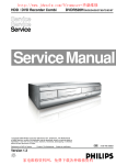
DVD-Video Recorder
DVDR615
DVDR615/69
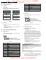
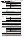
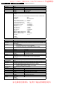
Contents
1
2
3
4
5
6
7
Page
Technical Specifications and Connection
Facilities
Safety Information, General Notes
Directions for Use
Mechanical Instructions
Diagnostic Software
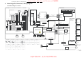
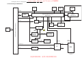
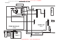
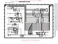
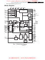
Block Diagrams, Waveforms, Wiring Diagram
Wiring Diagram
Waveforms
Testpoints
2
5
7
9
13
77
79
80
81
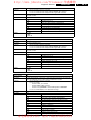
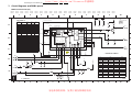
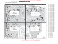
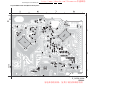
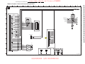
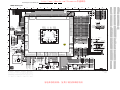
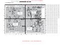
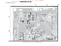
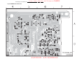
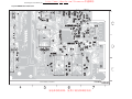
Circuit Diagrams and PWB Layouts
83
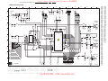
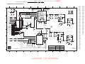
MOBO: Fronted Video (FV)
(Diagram 1)
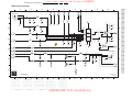
MOBO: In / Out Video (IOV)
(Diagram 2)
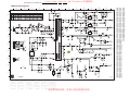
MOBO: In / Out Audio (IOA)
(Diagram 3)
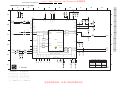
MOBO: Power Supply (PS)
(Diagram 4)
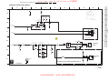
MOBO: Multi Sound Processing (MSP)(Diagram 5)
MOBO: Audio Converter(DAC_ADC) (Diagram 6)
MOBO: Digital In/Out 1(DIGIO1)
(Diagram 7)
MOBO: Color UniT (CU)
(Diagram 8)
MOBO: IR Blaster (IRB)
(Diagram 9)
MOBO: Digital In/Out 2(DIGIO2)
(Diagram 10)
Front: Keyboard (KEY)
(Diagram 11)
Front: Standby (STBY)
(Diagram 12)
Front: Open / Close (OPCL)
(Diagram 13)
Front: 5-Way Switch (5WSW)
(Diagram 14)
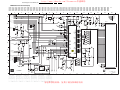
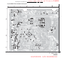
FEBE: FE OPU Interface
(Diagram 1)
FEBE: Fe Cheetah 2 Pre-processing (Diagram 2)
FEBE: FE Laconic Pre-processing
(Diagram 3)
FEBE: FE Drivers
(Diagram 4)
FEBE: FE Centaurus 1.5 Processor (Diagram 5)
FEBE: FE Supply / BE Interface
(Diagram 6)
FEBE: FE Tray Motor / Swich Conn. (Diagram 7)
FEBE: BE Chrysalis
(Diagram 8)
FEBE: BE Flash, EEPROM & SDRAM (Diagram 9)
83
84
85
86
87
88
89
90
91
98
99
101
102
103
104
105
106
107
108
109
110
111
112
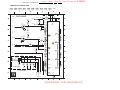
FEBE: BE DV In IEEE1394
FEBE: BE Video In Processing (VIP)
FEBE: BE Audio & Video In/Out
FEBE: BE Supply, Reset, UART, Enc.
8 Alignments
9 Circuit-, IC Descriptions and List
of Abbreviations
10 Spare Parts List
(Diagram 10)
(Diagram 11)
(Diagram 12)
(Diagram 13)
113
114
115
116
129
130
165
©
Copyright 2004 Philips Consumer Electronics B.V. Eindhoven, The Netherlands.
All rights reserved. No part of this publication may be reproduced, stored in a
retrieval system or transmitted, in any form or by any means, electronic,
mechanical, photocopying, or otherwise without the prior permission of Philips.
Published by KC 0439 Service PaCE
Printed in the Netherlands
Subject to modification
Version 1.0
家电维修资料网,免费下载各种维修资料
EN 3122 785 14220
http://www.jdwxzlw.com/?fromuser=华盛维修
EN 2
1.
DVDR615/69
Technical Specifications and Connection Facilities
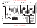
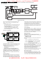
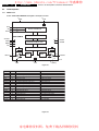
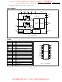
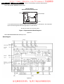
1. Technical Specifications and Connection Facilities
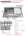
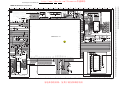
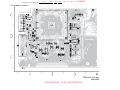
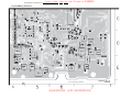
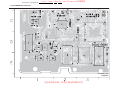
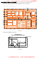
1.1
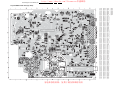
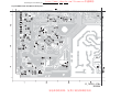
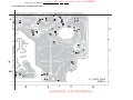
PCB Locations
1.2
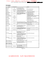
Diversity Matrix and Read and Write speed
1.4
Test equipment:Fluke 54200 TV Signal generator
Test streams:PAL BG Philips Standard test pattern
VFM RANGE
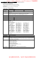
DVDR615/69
Module / Pcb Application
MOBO Board:
04 AP2
3139 248 82902
-
-
x
-
-
x
-
-
Front Board:
12NC:
3139 248 83071
VAU8041/21
DS version: E1_AV3_4
12NC:
9305 025 84121
pcb:
3104 128 09281
Drive:
AV3.5
Type of Disc (Function)
1.4.1
System:
PAL B/G, PAL D/K, PAL I
1.4.2
RF - Loop Through:
Frequency range
Gain: (ANT IN - ANT OUT)
Disc Rotation Speed
Read Speed CD
CAV 7x
Read Speed DVD
CAV 4x
Write Speed DVD+RW
ZCAV 2.4x
Write Speed DVD+R
ZCAV2.4x
1.3
RF Tuner
1.4.3
Radio Interference:
input voltage /3 tone method (+40
dB min)
1.4.4
: 45 MHz - 860 MHz
: +6 dB to -2dB
: 85dBµV
Receiver:
PLL tuning with AFC for optimum reception
Frequency range:
: 45.25 MHz - 857 MHz
Sensitivity at 40 dB S/N
: ≥ 60dBµV at 75Ω
(video unweighted )
General:
Mains voltage
: 198V-276V
Mains frequency
: 43 Hz - 63Hz
Power consumption (record)
: 27 W
Power consumption (AV loop through) : < 15W
Power consumption low power
stand-by
:
<3W
1.4.5
Video Performance:
Channel 25 / 503,25 MHz,
Test pattern: PAL BG PHILIPS standard test pattern,
RF Level 74 dBV
Measured on Cinch Out
家电维修资料网,免费下载各种维修资料
http://www.jdwxzlw.com/?fromuser=华盛维修
Technical Specifications and Connection Facilities
Frequency response:
Group delay ( 0.1 MHz - 4.4 MHz )
1.4.6
: 0.1- 4.00 MHz ± 3dB
: 0 nsec ± 150nsec
1.5.3
Audio Performance:
Audio Performance Analogue - HiFi:
Frequency response at Cinch Out
(L+R) output:
: 100 Hz - 12 kHz / 0±
3dB
S/N according to DIN 45405, 7, 1967 :
and PHILIPS standard test pattern
video signal:
: ≥ 50dB, unweighted
Harmonic distortion ( 1 kHz, ± 25
kHz deviation ):
: ≤ 1.5%
1.4.7
1.5.4
EN 3
Audio/Video Front Input Connectors
Audio - Cinch
Input voltage
Input impedance
: 2.2 Vrms
: >10kΩ
Video - Cinch
Input voltage
Input impedance
: 1 Vpp ± 3dB
: 75 Ω
Out 1
Component Video Cinch Y/Pb/Pr
according EIO-770-1-A, EIA-770-2-A
Tuning
Automatic Search Tuning
scanning time without antenna
stop level (vision carrier)
Maximum tuning error of a recalled
program
Maximum tuning error during
operation
:
:
Audio- Cinch
Output voltage
Output impedance
typ. 3 min.
≥ 37dBµV
: ± 62.5 kHz
1.5.5
: ± 100 kHz
Tuning Principle
automatic B,G, I and DK detection
manual selection in "STORE" mode
1.5
Analogue Inputs / Outputs
1.5.1
External 1
Audio - Cinch
Input voltage
Input impedance
: 2Vrms max.
: >10kΩ
Out 2
Audio- Cinch
Output voltage
Output impedance
: 2Vrms max.
: >10kΩ
Video- Cinch
Output voltage
Output impedance
: 1 Vpp ± 3dB
: 75 Ω
Video - YC (Hosiden)
According to IEC 933-5
Superimposed DC-level on pin 4 (load > 100kohm)
< 2.4V is detected as 4:3 aspect ratio
> 3.5V is detected as 16:9 aspect ratio
Output voltage Y
: 1Vpp +10/-15%
Output voltage C
: 300mVpp +1/-4dB
Component Video Cinch Y/Pb/Pr
according to EIO-770-1-A, EIA-770-2-A
: 1Vpp ± 3dB
: >10kΩ
1.6
1.5.2
1.
Video - YC (Hosiden)
According to IEC 933-5
Superimposed DC-level on pin 4 (load > 100kΩ)
< 2.4V is detected as 4:3 aspect ratio
> 3.5V is detected as 16:9 aspect ratio
Input voltage Y
: 1Vpp ± 3dB
Input impedance Y
: 75 Ω
Input voltage C
: burst 300 mVpp ± 3
dB
Input impedance C
: 75 Ω
Audio Performance NICAM:
Frequency response at Cinch Out
(L+R) output:
: 40 Hz - 15 kHz 0 ±
3dB
S/N according to DIN 45405, 7, 1967 :
and PHILIPS standard test pattern
video signal:
: ≥ 60 dB unweighted
Harmonic distortion (1 kHz):
: ≤ 0.5 %
DVDR615/69
Video Performance
External 2
All outputs loaded with 75 Ohm
SNR measurements over full bandwidth without weighting.
Audio- Cinch
Output voltage
Output impedance
: 2Vrms max.
: >10kΩ
Video- Cinch
Output voltage
Output impedance
: 1 Vpp ± 3dB
: 75 Ω
Video - YC (Hosiden)
According to IEC 933-5
Superimposed DC-level on pin 4 (load > 100kΩ)
< 2.4V is detected as 4:3 aspect ratio
> 3.5V is detected as 16:9 aspect ratio
Input voltage Y
:1Vpp ± 3dB
Input impedance Y
:75 Ω
Input voltage C
:burst 300 mVpp ± 3 dB
Input impedance C
:75 Ω
1.6.1
SCART (RGB)
SNR
Bandwidth
1.7
Audio Performance CD
1.7.1
Cinch Output Rear
Output voltage 2 channel mode
Channel unbalance (1kHz)
Crosstalk 1kHz
Crosstalk 16Hz-20kHz
Frequency response
Signal to noise ratio
Dynamic range 1kHz
Distortion and noise 1kHz
家电维修资料网,免费下载各种维修资料
: > 48 dB
: 4.8 MHz − 3dB
:
:
:
:
:
:
:
:
2Vrms ± 1dB
<0.22dB
>100dB
>87dB
±0.2dB max
>85 dB
>83dB
>83dB
http://www.jdwxzlw.com/?fromuser=华盛维修
EN 4
1.
DVDR615/69
Distortion and noise 16Hz-20kHz
Intermodulation distortion
Mute
Outband attenuation:
1.8
Digital Audio Output
1.8.1
Coaxial
CDDA/ LPCM (incl MPEG1)
MPEG2, AC3 audio
DTS
1.8.2
:
:
:
:
Technical Specifications and Connection Facilities
>75dB
>70dB
>95dB
>40dB above 30kHz
: according IEC958
: according IEC1937
: according IEC1937,
amendment 1
Optical
CDDA/ LPCM (incl MPEG1)
MPEG2, AC3
DTS
: according IEC958
: according IEC937
: according IEC937,
amendment 1
1.9
Digital Video Input (IEEE 1394)
1.9.1
Applicable Standards
Implementation according:
IEEE Std 1394-1995
IEC 61883 - Part 1
IEC 61883 - Part 2 SD-DVCR (02-01-1997)
Specification of consumer use digital VCR’s using 6.3 mm
magnetic tape - dec.1994
Mechanical connection according:
Annex A of 61883-1
1.10 Dimensions and Weight
Height of feet
Apparatus tray closed
Apparatus tray open
Weight without packaging
Weight in packaging
:
:
:
5.5mm
WxDxH :435 x 285x 65mm
WxDxH :435 x 422x 65mm
: app. 4 kg ± 0.5 kg
: app. 6.5 kg
1.11 Laser Output Power & Wavelength
1.11.1 DVD
Output power during reading
Output power during writing
Wavelength
: 0.8mW
: 20mW
: 660nm
1.11.2 CD
Output power
Wavelength
: 0.3mW
: 780nm
家电维修资料网,免费下载各种维修资料
http://www.jdwxzlw.com/?fromuser=华盛维修
Safety Information, General Notes
DVDR615/69
2.
EN 5
2. Safety Information, General Notes
2.1
Safety Instructions
2.2
Warnings
2.1.1
General Safety
2.2.1
General
Safety regulations require that during a repair:
• Connect the unit to the mains via an isolation transformer.
• Replace safety components, indicated by the symbol ,
only by components identical to the original ones. Any
other component substitution (other than original type) may
increase risk of fire or electrical shock hazard.
Safety regulations require that after a repair, you must return
the unit in its original condition. Pay, in particular, attention to
the following points:
• Route the wires/cables correctly, and fix them with the
mounted cable clamps.
• Check the insulation of the mains lead for external
damage.
• Check the electrical DC resistance between the mains plug
and the secondary side:
1. Unplug the mains cord, and connect a wire between
the two pins of the mains plug.
2. Set the mains switch to the 'on' position (keep the
mains cord unplugged!).
3. Measure the resistance value between the mains plug
and the front panel, controls, and chassis bottom.
4. Repair or correct unit when the resistance
measurement is less than 1 MΩ.
5. Verify this, before you return the unit to the customer/
user (ref. UL-standard no. 1492).
6. Switch the unit ‘off’, and remove the wire between the
two pins of the mains plug.
•
•
•
2.2.2
Laser
•
•
2.1.2
Laser Safety
•
This unit employs a laser. Only qualified service personnel may
remove the cover, or attempt to service this device (due to
possible eye injury).
Laser Device Unit
Type
: Semiconductor laser
GaAlAs
: 650 nm (DVD)
: 780 nm (VCD/CD)
: 20 mW
(DVD+RW writing)
: 0.8 mW
(DVD reading)
: 0.3 mW
(VCD/CD reading)
: 60 degree
Wavelength
Output Power
Beam divergence
All ICs and many other semiconductors are susceptible to
electrostatic discharges (ESD, ). Careless handling
during repair can reduce life drastically. Make sure that,
during repair, you are at the same potential as the mass of
the set by a wristband with resistance. Keep components
and tools at this same potential.
Available ESD protection equipment:
– Complete kit ESD3 (small tablemat, wristband,
connection box, extension cable and earth cable) 4822
310 10671.
– Wristband tester 4822 344 13999.
Be careful during measurements in the live voltage section.
The primary side of the power supply (pos. 1005), including
the heatsink, carries live mains voltage when you connect
the player to the mains (even when the player is 'off'!). It is
possible to touch copper tracks and/or components in this
unshielded primary area, when you service the player.
Service personnel must take precautions to prevent
touching this area or components in this area. A 'lightning
stroke' and a stripe-marked printing on the printed wiring
board, indicate the primary side of the power supply.
Never replace modules, or components, while the unit is
‘on’.
•
The use of optical instruments with this product, will
increase eye hazard.
Only qualified service personnel may remove the cover or
attempt to service this device, due to possible eye injury.
Repair handling should take place as much as possible
with a disc loaded inside the player.
Text below is placed inside the unit, on the laser cover
shield:
CAUTION VISIBLE AND INVISIBLE LASER RADIATI ON WHEN OPEN AVO ID EXPOSURE TO BEAM
ADVARSEL SYNLIG OG USYNLIG LASERSTRÅLING VED ÅBNING UNDGÅ UDSÆTTELSE FOR STRÅLING
!
ADVARSEL SYNLIG OG USYNLIG LASERSTRÅLING NÅR DEKSEL
ÅPNES UNNGÅ EKSPONERING FOR STRÅLEN
VARNING SYNLIG OCH OSYNLIG LASERSTRÅLNING NÄR DENNA DEL ÄR ÖPPNAD BETRAKTA EJ STRÅLEN
VARO! AVATT AESSA OLET ALTTIINA NÄKYVÄLLE JA NÄKYMÄTT ÖMÄLLE LASER SÄTEILYLLE. ÄLÄ KAT SO SÄT EESEEN
VORSICHT SICHTBARE UND UNSICHTBARE LASERSTRAHLUNG WENN ABDECKUNG GEÖFFNET NICHT DEM STRAHL AUSSETSEN
DANGER VISIBLE AND INVISIBLE LASER RADIATI ON WHEN OPEN AVO ID DIRECT EXPOSURE TO BEAM
AT TENTION RAYO NNEMENT LASER VISIBLE ET INVISIBLE EN CAS D'OUVERTURE EXPOSITION DANGEREUSE AU FAISCEAU
Figure 2-2
2.2.3
Notes
Dolby
Manufactered under licence from Dolby Laboratories. “Dolby”,
“Pro Logic” and the double-D symbol are trademarks of Dolby
Laboratories. Confidential Unpublished Works.
©1992-1997 Dolby Laboratories, Inc. All rights reserved.
Figure 2-3
Figure 2-1
Note: Use of controls or adjustments or performance of
procedure other than those specified herein, may result in
hazardous radiation exposure. Avoid direct exposure to beam.
Trusurround
TRUSURROUND, SRS and symbol (fig 2-4) are trademarks of
SRS Labs, Inc. TRUSURROUND technology is manufactured
under licence frm SRS labs, Inc.
Figure 2-4
家电维修资料网,免费下载各种维修资料
http://www.jdwxzlw.com/?fromuser=华盛维修
EN 6
2.
DVDR615/69
Safety Information, General Notes
Video Plus
“Video Plus+” and “PlusCode” are registered trademarks of the
Gemstar Development Corporation. The “Video Plus+” system
is manufactored under licence from the Gemstar Development
Corporation.
Figure 2-5
Macrovision
This product incorporates copyright protection technology that
is protected by method claims of certain U.S. patents and other
intellectual property rights owned by Macrovision Corporation
and other rights owners.
Use of this copyright protection technology must be autorized
by Macrovision Corporation, and is intended for home and
other limited viewing uses only unless otherwise authorized by
Macrovision Corporation. Reverse engineering or disassembly
is prohibited.
家电维修资料网,免费下载各种维修资料
http://www.jdwxzlw.com/?fromuser=华盛维修
Directions For Use
3.
DVDR615/69
3.
EN 7
Directions For Use
The following excerpt of the Quick Use Guide serves as an introduction to the set.
The complete Direction for Use can be downloaded in different languages from the internet site of Philips Customer Care Center:
www.p4c.philips.com
QUICK USE GUIDE
DVDR610
DVDR615
DVDR616
12nc: 3139 246 14151
LANGUAGE AND COUNTRY
Select Language and Country
ANTENNA/
CABLE SIGNAL
Menu
English
Spanish
French
Language
Country
4
Done
5
TV FORMAT
1
Select your TV format
2
4
3
TV format
Done
CHANNEL SEARCH
Automatic channel search will find and
store all channels. Make sure to connect
the Antenna.
Channel Search
6
Start
TIME AND DATE
Check time and date and correct if
necessary
5
1
1
2
3
4
5
Connect DVD recorder
Remove the antenna cable plug from your TV (or Satellite
Receiver/Cable Box). Connect it to the ANTENNA input
socket at the back of the DVD recorder.
Use the supplied antenna cable to connect the DVD
recorder’s TV output socket to the antenna input socket at
the back of your TV set
Use the supplied AV cables (yellow plug) to connect the
DVD recorder’s VIDEO (CVBS) (OUT 2) socket to the
Video In socket at the back of your TV set.
3
1
2
Time
09:00
Date
30.06.2004
Done
OK
1.3
CH-
7
8
CH+
IS THE TV ON?
1
Skip Search
DVD recorder back panel
2
4:3 Panscan
4:3 Letterbox
16:9
CH+
3
CH-
Start first installation
Press STANDBY-ON 2 on the DVD recorder to switch
it on.
Switch on the TV set and select the correct video in channel,
the First Installation menu appears on the TV.
NO PICTURE! Press the TV/AV button or CHANNEL 3 4
button on the TV to select the correct video in channel, for
example, 'EXT', '0', or 'AV'.
3
Use the supplied AV cables (red/white plugs) to connect the
DVD recorder’s AUDIO L/R (OUT 2) socket to the audio
input socket at the back of your TV set.
Connect the power cable from the DVD recorder’s
~ MAINS to the power supply.
4
Helpful Hint:
If your TV does not have the above-mentioned
connectors, please refer to the user manual for more
information on others possible connection to your
TV set.
5
Press 3 4 to select an item in the menu.
Press 2 to access the selected item’s options.
Press 1 to confirm your selection.
When you complete, select { Done } in the menu and press
OK to continue.
{ Language and Country } menu appears.
{ Language } – select on-screen display language.
{ Country } – select country of your residence.
{ TV Format } menu appears.
{ TV Format } – select TV screen display.
6
{ Channel Search } menu appears.
Press OK to start automatic TV channel search.
Once the TV channel search complete, the total number of
channels found appears.
2
Prepare the remote control
7
If the time and date shown on the TV are not correct,
press 2 to enter the respective time/date field. Press 3 4 to
change the first digit and press 2 to go to the next digit field.
Once complete, press OK to confirm.
3
8
1
{ Time and Date } menu appears.
Press 4 to select { Done } and press OK to save the changes.
➜ The first installation is now complete.
2
The DVD recorder is ready for use!
See next page for basic recording and playback.
家电维修资料网,免费下载各种维修资料
http://www.jdwxzlw.com/?fromuser=华盛维修
EN 8
3.
Directions For Use
DVDR615/69
... cont.
SUPER VIDEO
1.3
1.3
CH-
CH+
CH-
CH+
{0}
34
1234
OK
CH+
CH+
EDIT
CHCH-
PLAY
2
4
1
2
Start manual recording
Insert a recordable DVD+R(W) with the label side facing up.
Press TUNER on the remote control to see the TV
programmes, then press 3 4 to select the programme
number you wish to record.
5
1
2
➜ If you wish to record from additional device (e.g.Video Cassette
Recorder), press button 3 4 on the remote control to select the
correspond external input channel.
For example, select { EXT2 } if you have connected the VCR to
IN-EXT2 socket at the back of the DVD recorder.
3
Press REC MODE to select a desired recording mode. It
defines the picture quality and the maximum recording time
for a disc.
Record
Mode
●
Insert a disc with the label side facing up.
Playback will start automatically.
➜ If a dialogue appears on the TV showing { Do you want to
access the disc content }, press 3 4 to select { Yes } to show the
disc content or { No } to start playback, then press OK to confirm
➜ If a disc menu appears, press 1 2 3 4 to navigate within the
menu, highlight a title and press OK or PLAY 2 to start playback.
NO SOUND! Connect the AUDIO L/R (red/white) sockets at
the back of the DVD recorder to the correspond AUDIO input
sockets on a TV set, stereo system or receiver. Turn on the
connected system and select the appropriate channel.
3
To stop playback, press STOP 9.
Maximum Recording
Time per Disc
M1
High quality (HQ)
1 hour
M2
M2x
M3
DVD quality-Standard Play (SP)
DVD quality-Standard Play Plus (SP+)
2 hours
2.5 hours
3 hours
M4
M6
M8
4
Picture Quality
Start Playback
S-VHS quality-Long Play (LP)
VHS quality-Extended Play (EP)
VHS quality-Super Long Play (SLP)
VHS quality-Super Extended Play (SEP)
To watch the TV programmes
1
4 hours
6 hours
8 hours
Press REC 0 to start recording.
If required, you can press REC 0 twice to start a
30-minute recording. Each time you press REC 0 button,
you will add 30 minutes to the recording time.
5
During recording, you may press PAUSE ; to pause the
recording and press REC 0 to continue.
6
To stop the recording, press STOP 9.
➜ Wait until the message disappears from the display panel before
you remove the disc.
Press TUNER on the remote control, then press 3 4 to
select the programme number.
To play a DVD+R on other DVD players, you
must finalise it first
1
2
Press EDIT on the remote control.
Press 3 4 to select { Finalise } in the menu, then press
OK.
Once a DVD+R is finalised, no further recording or
editing is possible. Unfinalising a DVD+R is not
possible.
Detailed playback features and additional functions are described in the
accompanying user manual.
家电维修资料网,免费下载各种维修资料
http://www.jdwxzlw.com/?fromuser=华盛维修
Mechanical Instructions
DVDR615/69
4.
EN 9
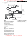
4. Mechanical Instructions
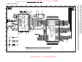
4.1
Dismantling and Assembly of the Set
For item numbers please see the exploded views in chapter 10.
4.1.1
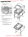
Front Panel Assembly
–
–
–
–
After removing the top cover, remove tray front 134+138,
see picture 4-1
Remove the three screws 188
Release the two snap hooks on the sides and remove the
front assembly
Remove the 4 screws 186 to remove the front plate 184,
see picture 4-2
4.1.2
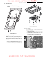
Basic Engine VAU8041
–
–
–
–
–
–
Remove the Front Panel Assembly as given in 4.1.1
Remove the 6 screws 260, 269 to free the Basic Engine
Remove the dust cover assembly 147 and 148
Loosen 2 screws to remove bracket 256
Loosen 4 screws to remove the Basic Engine metal casing
Place the Basic Engine in the service position
Figure 4-3
Figure 4-1
Figure 4-2
Figure 4-4
家电维修资料网,免费下载各种维修资料
http://www.jdwxzlw.com/?fromuser=华盛维修
EN 10
4.1.3
4.
DVDR615/69
Mechanical Instructions
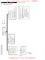
MOBO Board
–
–
–
–
Remove the Front Panel assembly as given in 4.1.1
Remove 6 screws 246 and 254
Remove 4 screws 270
Service position is achieved by flipping the MOBO board
above the Basic Engine
2
2
Figure 4-5
4.2
Dismantling and assembly of the VAU8041
Module
4.2.1
General
Follow the dismantling instructions in described order.
Do not place the unit with its PCB on a hard surface (e.g. table),
as it could damage the components on it.
Always place something soft (a towel or foam cushion) under it.
Never touch the lens of the OPU.
Take sufficient ESD measures during handling.
1
1
1
1
Figure 4-6 VAU8041 Module dismantling
4.2.2
Dismantling the FEBE Board
–
–
Remove 4 screws to remove the metal case 150+180
Remove 2 screws to separate the FEBE board 179 from
the main Loader/Drive assembly
Note: After exchange of the PCB (or the Drive mechanism)
the complete VAU8041 has to be adjusted! Refer to
chapter 8 for adjustment instructions!
2
1
1
Figure 4-7 Remove FEBE board
家电维修资料网,免费下载各种维修资料
http://www.jdwxzlw.com/?fromuser=华盛维修
Mechanical Instructions
4.2.3
DVDR615/69
4.
EN 11
Dismantling the Tray
–
–
Remove the encasing as described in 4.2.2
Disengage the two holders that fix the tray [1] and pull out
the tray [2]
2
1
1
1
1
1
1
Figure 4-9 Remove DVD-M
4.2.5
2
Figure 4-8 Remove Tray
4.2.4
DVD-M (Drive Mechanism)
Re - assembly
To re-assemble the module, do all processes in reverse order.
Take care of the following:
• Heat Paths:Put the 5 heat paths (gray rubber pieces) back
to their position on the ICs.
• Complete module: Place all wires/cables in their original
positions
• Emergency opening slot: Be sure that the slot for the
emergency tray opener is covered by adhesive tape!
Caution: Never try to align or repair the DVD-Module itself!
Only the factory can do this properly. Service engineers are
only allowed to exchange the sledge motor assy.
After Exchanging the DVD-M (or the PCB) the complete drive
has to be adjusted! Refer to chapter 8 for adjustment
instructions!
–
–
–
Remove encasing and FEBE board as described in 4.2.2
Remove the Sealing strip 5 by uncatching it
Loosen the 4 screws/washer [1] to remove the DVD-M [2]
Figure 4-10 Heat Paths
家电维修资料网,免费下载各种维修资料
⇒ demount the board
⇒ Remove screws 172
of DV input cable
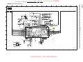
DVDR BASIC ENGINE 1004
⇒ It is possible to unlock the tray by means
of a screwdriver via a slot in the
front and frame at the underside.
.
Push
the white pin of the slider at the
underside of the basic engine to the left
(seen from the front)
⇒ Open the unlocked tray.
In case the loader is defective and cannot be
opened electrically, you can open the tray
as follows:
Manual opening of tray and removal of
tray front 134 + 138
⇒ Remove 6 screws 260 and 269
(assembly -> frame 224)
⇒ Remove 2 screws 262
(assembly -> support bracket 256)
⇒ Uncatch dust cover assembly 147 + 148
from DVDR Basic Engine
⇒ Remove Front Panel assembly
⇒ Remove all the connections
DVDR615/69
Front Control board
⇒ Remove 2 screws 176
(board → front)
⇒ unlock the front from the
frame by releasing 2 snaps
on left and right
⇒ remove 4 screws 186 to
remove the plate front 184
demounting
mounting
4.3
4.
- Remove the Front Panel assembly
- Remove the connections
- Remove 6 screws 246, 254
(board => backplate)
⇒ remove 4 screws 270
(board → frame)
⇒ demount the board
MOBO board 1001
Cover 196
⇒ Remove 7 screws 220 & 240
⇒ Lift the cover
to remove
EN 12
Front Panel Assembly
⇒ open the tray and remove the
tray front 134 + 138
⇒ remove 3 screws 188
(front assy → frame 224)
See exploded view for item numbers
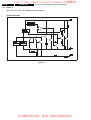
DISMANTLING INSTRUCTIONS
http://www.jdwxzlw.com/?fromuser=华盛维修
Mechanical Instructions
Dismantling Instructions
TR 06003_003
300504
Figure 4-11
家电维修资料网,免费下载各种维修资料
http://www.jdwxzlw.com/?fromuser=华盛维修
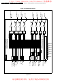
Diagnostic Software
DVDR615/69
5.
EN 13
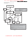
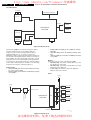
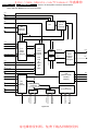
5. Diagnostic Software
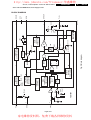
Due to the complexity of the DVD recorder, the time to find a
defect in the recorder can become long. To reduce this time,
the recorder has been equipped with Diagnostic and Service
software (DS). The DS offers functionality to diagnose the
DVDR hardware and tests the following:
• Interconnections between components
• Accessibility of components
• Functionality of the audio and video paths
This functionality can be accessed via several interfaces:
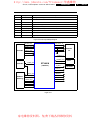
5.1.2
Structure
Unplug the power cord
Hold key <PLAY> pressed
while you plug the recorder
During the test, the display will show
the a sequence of nuclei under test
1. End user/Dealer script interface
2. Command Interface
SET O.K.?
5.1
End User/Dealer Script Interface
5.1.1
Description
The End user/Dealer script interface gives a diagnosis on a
stand alone DVD recorder. During this mode, a number of
hardware tests (nuclei) are automatically executed to check if
the recorder is faulty. The diagnosis is simply a "fail" or "pass"
message. If the message "FAIL" appears on the display, there
is apparently a failure in the recorder. If the message "PASS"
appears, the nuclei in this mode have been executed
successfully. There can be still a failure in the recorder
because the nuclei in this mode don't cover the complete
functionality of the recorder.
5.1.3
NO
YES
To exit DEALER SCRIPT, unplug the power cord
TR 18029_001
120304
Figure 5-1
The End use/Dealer script executes all diagnostic nuclei that
do not need any user interaction and are meaningful on a
standalone DVD recorder.
Contents
Included tests:
1.DS_ANAB_COMMUNICATIONECHO_NUC
2.DS_DCB_COMMUNICATIONECHO_NUC
3. DS_BROM_COMMUNICATION_NUC
4. DS_SYS_SETTINGSDISPLAY_NUC
5. DS_CHR_DEVTYPEGET_NUC
6. DS_CHR_INT_PIC_NUC
7. DS_CHR_DMA_NUC
8. DS_BROM_WRITEREAD_NUC
9. DS_NVRAM_COMMUNICATION_NUC
10. DS_NVRAM_WRITEREAD_NUC
11. DS_SDRAM_WRITEREADFAST_NUC
12. DS_FLASH_WRITEREAD_NUC
13.DS_FLASH_CHECKSUMPROGRAM_NUC
14.DS_SYS_HARDWAREVERSIONGET_NUC
15. DS_VIP_DEVTYPEGET_NUC
16. DS_VIP_COMMUNICATION_NUC
17. DS_DVIO_LINKDEVTYPEGET_NUC
18. DS_DVIO_PHYDEVTYPEGET_NUC
19. DS_DVIO_LINKCOMMUNICATION_NUC
20. DS_DVIO_PHYCOMMUNICATION_NUC
21.DS_PSCAN_COMMUNICATIONDENC_NUC
22.DS_PSCAN_COMMUNICATIONDEINTERLACER_NUC
23. DS_BE_COMMUNICATIONECHO_NUC
24.DS_ANAB_COMMUNICATIONIICNVRAM_NUC
25.DS_ANAB_COMMUNICATIONIICTUNER_NUC
26.DS_ANAB_COMMUNICATIONIICSOUNDPROCESSOR_NUC
27.DS_ANAB_COMMUNICATIONIICAVSELECTOR_NUC
28. DS_ANAB_CHECKSUMPROGRAM_NUC
家电维修资料网,免费下载各种维修资料
http://www.jdwxzlw.com/?fromuser=华盛维修
EN 14
5.2
5.2.1
5.
Diagnostic Software
DVDR615/69
Player Script Interface
Trade Mode
15*
HDMI
16
Analogue Slave Processor
17
Analogue Board EEPROM
18
Video Matrix
TRADE MODE
19
Audio Matrix
When the recorder is in Trade Mode, the recorder cannot be
controlled by means of the front key buttons, but only by means
of the remote control.
20
Front End
21*
Hard Disk
22*
Digital Terrestrial Tuner Module
IF TRADE MODE OFF
IF TRADE MODE ON
* Not applicable for DVDR610, DVDR615 & DVDR616 Range
UNPLUG THE RECORDER
UNPLUG THE RECORDER
5.3.2
PRESS 2 KEYS
SIMULTANEOUSLY
PRESS 2 KEYS
SIMULTANEOUSLY
<STOP> + <OPEN/CLOSE>
<STOP> + <OPEN/CLOSE>
PLUG THE RECORDER
PLUG THE RECORDER
RECORDER IS IN TRADE MODE
WHEN PRESSING FRONT
KEYS, THE RECORDER
DOESN'T RESPOND
RECORDER IS IN NORMAL MODE
WHEN PRESSING FRONT
KEYS, THE RECORDER
WILL RESPOND
Each nucleus returns an error code. This code contains six
numerals, which means:
[ XX YY ZZ ]
Error code
Nucleus number
Nucleus group number
CL 16532095_071.eps
150801
Figure 5-2
5.2.2
CL 06532152_013.eps
051200
Virgin mode
Figure 5-4
If you want that the recorder starts up in Virgin mode, follow this
procedure:
• Unplug the recorder
• plug the recorder again while you keep the STAND BY/ON
key pressed
• the set starts up in Virgin mode.
5.3
Menu and Command Mode Interface
5.3.1
Nuclei Numeration
Each nucleus has a unique number of four digits. This number
is the input of the command mode.
[ XX YY
Error Handling
]
Nucleus number
Nucleus group number
CL 06532152_012.eps
051200
Figure 5-3
Group number Group name
0
Scripts
1
Codec (e.g. Chrysalis, Leco)
2
Boot EEPROM
3
NVRAM
4
SDRAM
5
Flash
6
Video Input Processor
7
DVIO
8*
Progressive Scan
9
Basic Engine
10*
Display and Control Board
11*
Analogue Board
12
System
13*
Electronic Program Guide Board
14*
PCMCIA
The nucleus group numbers and nucleus numbers are the
same as above.
5.3.3
Command Mode Interface
Set-Up Physical Interface Components
Hardware required:
• Service PC
• one free COM port on the Service PC
• special cable to connect DVD recorder to Service PC
The service PC must have a terminal emulation program (e.g.
Hyperterminal) installed and must have a free COM port (e.g.
COM1). Activate the terminal emulation program and check
that the port settings for the free COM port are: 19200 bps, 8
data bits, no parity, 1 stop bit and no flow control. The free COM
port must be connected via a special cable to the RS232 port
of the DVD recorder. This special cable will also connect the
test pin, which is available on the connector, to ground (i.e.
activate test pin).
Code number of PC interface cable: 3122 785 90017
Activation of Diagnostic Software
1. Pull the mains cord from the recorder and reconnect it
again (reboot).
2. The next welcome message will appear on the PC:
Welcome screen D&S program
Figure 5-5
Now, the prompt 'DS:>' will appear. The diagnostic software is
now ready to receive commands. The commands that can be
given are the numbers of the nuclei. If you see above shown
screen, continue with paragraph 'Nuclei Codes'.
家电维修资料网,免费下载各种维修资料
http://www.jdwxzlw.com/?fromuser=华盛维修
Diagnostic Software
3. It is possible that the next messages will appear when
starting the DVD+RW for the first time
DVDR615/69
5.
EN 15
Enter "Y" to program a safe string. With this automatically
generated string the board will work in principle but it has to be
checked if all board settings were detected correctly.
Error messages D&S program
Diversity String Input
4. Execute nucleus 1226 to enter the string. Please see
chapter 8.4 for details
Nucleus 1226 execution with string
Figure 5-6a
Error messages D&S program
Figure 5-7
5. To check if the hardware info is filled correctly, you can
execute nucleus 1228.
Nucleus 1228 info example
Figure 5-6b
In these cases, the boot EEPROM of the Digital Board does not
contain the required string with the hardware information. To
update the Digital Board with the correct string, nucleus 1226
must be executed.
See next section 'Diversity String Input'.
There can also be the next error message.
Figure 5-8
6. Exit the 'Terminal' program.
7. Reboot the DVD recorder to allow the software to start.
Figure 5-6c
家电维修资料网,免费下载各种维修资料
http://www.jdwxzlw.com/?fromuser=华盛维修
EN 16
5.
Diagnostic Software
DVDR615/69
Command overview Digital Board
Below you will find an overview of the nuclei, their numbers,
and their error codes. This overview is preliminary and subject
to modifications.
Note: AV3 in the overview includes also the AV3.5 drive.
CODEC HOST CONTROLLER (CHR)
Nucleus Name
DS_CHR_DevTypeGet
Nucleus Number
100
Description
Retrieves the device id, the module ids and revisions of the Codec and returns them to the
stdout port.
Technical
Determine the codec id by means of comparing version ids of the modules.Read the module-id register of every module and display it to the user.
Execution Time
Less than 1 second.
User Input
None
Error
Number
Description
10000
Getting the information succeeded
10001
Wrong codec id detected
Example
DS:> 100
010000:
Device ID 7100
Codec ID PNX7100_C
F-BCU (0x0102) 1.0
SIF (0x013b) 1.0
(0x010a) 1.0
DEBUG (0x0116) 0.0
UART2 (0x0107) 0.1
I2C1 (0x0105) 0.1
DISP0 (0xa015) 1.12
SPU (0xa00e) 0.0
CCIR (0x0139) 1.0
DV (0xa00c) 0.0
SGDX (0xa008) 1.0
ACOMP (0xa000) 1.0
SCR (0x0000) 0.0
AUDIO0 (0xa015) 1.12
INTC (0x011d) 1.0
EJTAG (0x0104) 0.1
CONFIG (0x013f) 1.1
UART0 (0x0107) 0.1
UART3 (0x0107) 0.1
GPIO (0x013c) 1.0
DISP1 (0xa00f) 1.1
MIXER (0x0137) 1.0
VDEC (0x0133) 0.2
BEI (0xa00a) 0.1
BYTE (0xa00b) 0.1
VFE (0xa001) 0.1
SIFF (0xa011) 0.1
AUDIO1 (0xa00f) 1.1
PCI-XIO(0x0113) 1.0
S-BCU (0x0102) 1.0
RESET (0x0123) 1.0
UART1 (0x0107) 0.1
I2C0 (0x0105) 0.1
SYNC (0x013a) 1.0
OSD (0x0136) 0.1
DENC (0x0138) 1.0
PARSER (0xa00d) 0.0
IDE (0xa009) 0.1
OUTPUT (0xa003) 1.0
VCOMP (0xa002) 1.0
WMD (0xa010) 0.0
PSCAN (0xa018) 0.1
Test OK @
Nucleus Name
DS_CHR_TestImageOn
Nucleus Number
101
Description
Generates a test-image of a selected video standard on selected video output on the digital
board. When no input is given, the default values will be used (see user input description below). Make sure to use the proper nuclei to route the video signal on the analogue board to get
the videosignal to the proper output.
Technical
-Validate the user input.
-Initialise the SYNC module.
-Initialise the DISPLAY module.
-Initialise the MIXER module.
-Initialise the DENC module.
-Set the selected video standard.
-Generate the selected test image in memory.
-Start the DISPLAY module.
-Start the MIXER module.
-Start the DENC module according to the selected test image id.
Execution Time
6 seconds.
家电维修资料网,免费下载各种维修资料
http://www.jdwxzlw.com/?fromuser=华盛维修
Diagnostic Software
Nucleus Name
User Input
DVDR615/69
DS_CHR_TestImageOn
The user has to decide which test image, video standard and video output must be used:
Test image id:
0
VERTICAL_COLOURBAR (default)
1
HORIZONTAL_COLOURBAR
2
WHITE
3
YELLOW
4
CYAN
5
GREEN
6
MAGENTA
7
RED
8
BLUE
9
BLACK
10GRAY
11TEST_IMAGE_FOR_PROGRESSIVE_SCAN
Video standard:
PAL
(default)
NTSC
Video output
ALL
CVBS and YC and RGB (default)
CVBS
YC
RGB
YUV
PSCAN
progressive scan
Error
Number
Example
Description
10100
Generating the test image succeeded.
10101
Invalid input was provided.
10102
The Codec SYNC-module cannot be initialised.
10103
The Codec MIXER-module cannot be initialised.
10104
The Codec VPP-module cannot be initialised.
10105
The Codec DENC-module cannot be initialised.
10106
The digital board hardware information is corrupt
DS:> 101
010100:
Test OK @
DS:> 101 0 pal cvbs
010100:
Test OK @
DS:> 101 4 ntsc yc
010100:
Test OK @
Nucleus Name
DS_CHR_TestImageOff
Nucleus Number
102
Description
Switches the test-image off.
Technical
Stop the DENC module.
Execution Time
Less than 1 second.
User Input
None
Error
Number
Description
10200
Stopping the test image generation succeeded
10201
The Codec DENC-module failed.
Example
Nucleus Name
DS:> 102
010200:
Test OK @
DS_CHR_SineOn
Nucleus Number
103
Description
Generate an audio sine signal on the audio output of the digital board. Note: Left channel
6kHz, right channel 12 kHz sine. Make sure to route the signal first.
家电维修资料网,免费下载各种维修资料
5.
EN 17
http://www.jdwxzlw.com/?fromuser=华盛维修
EN 18
5.
Diagnostic Software
DVDR615/69
Technical
-
De-mute the analogue board
Set fifo parameters for audio
Set the volume
Set the I2S outputs and configuration paths
Set the decoder mode
Configure the audio decoder
Put the AC3 audio in the fifo
Send ‘prepare’ command to the audio decoder
Send ‘play’ command to the audio decoder
Execution Time
Less than 1 second
User Input
None
Error
Number
Description
10300
The sine signal was successfully generated
Example
10301
The analogue board could not be de-muted
10302
The audio decoder did not initialise
10303
The dsp2 of the audio decoder did not configure
10304
The dsp1 of the audio decoder did not configure
10305
There was a delay-error before starting
10306
Wrong input was given to the decoder function
10307
Wrong input was given to the decoder function @@@@@
10308
The audio decoder did not get into the 'prepared' state
DS:> 103
010300:
Test OK @
Nucleus Name
DS_CHR_SineOff
Nucleus Number
104
Description
Stop generating the audio sine signal
Technical
-
Execution Time
Less than 1 second.
Reset the audio block of the Codec
User Input
None
Error
Number
Description
10400
Switching off the audio sine signal succeeded
10401
Failed to reset the audio decoder
Example
DS:> 104
010400:
Test OK @
Nucleus Name
DS_CHR_SineBurst
Nucleus Number
105
Description
Generate an audio sine signal on the audio output of the digital board for 4 seconds.
Note: Left channel 6kHz, right channel 12 kHz sine with some known hick-ups
Technical
-
Execution Time
4 seconds
Call the DS_CHR_SineOn nucleus
Delay for 4 seconds
Call the DS_CHR_SineOff nucleus
User Input
None
Error
Number
Description
10500
The sine signal burst was successfully generated
Example
10501
The delay did not succeed during the burst
10502
The audio sine could not be generated
DS:> 105
010500:
Test OK @
Nucleus Name
DS_CHR_MuteOn
Nucleus Number
106
Description
Mute the audio outputs of the digital board
Technical
- Send the 'Mute' command to the audio decoder
Execution Time
Less than 1 second.
User Input
None
Error
Number
Description
10600
Muting the audio succeeded
家电维修资料网,免费下载各种维修资料
http://www.jdwxzlw.com/?fromuser=华盛维修
Diagnostic Software
Example
DS:> 106
010600:
Test OK @
Nucleus Name
DS_CHR_MuteOff
Nucleus Number
107
Description
De-mute the audio outputs of the digital board
Technical
-
Execution Time
Less than 1 second.
User Input
None
Error
Number
Description
10700
De-muting the audio succeeded
DVDR615/69
Send the ‘DeMute’ command to the audio decoder
Example
DS:> 107
010700:
Test OK @
Nucleus Name
DS_CHR_DvLedOn
Nucleus Number
108
Description
Check the connection to the DV-LED on the digital board by switching it on
Technical
-
Execution Time
Less than 1 second.
User Input
None
Error
Number
Description
10800
Switching the DV-LED on succeeded
10801
Switching the DV-LED on failed
Write to the PIO pin to light the DV LED
Example
DS:> 108
010800:
Test OK @
Nucleus Name
DS_CHR_DvLedOff
Nucleus Number
109
Description
Switch off the DV-LED on the digital board
Technical
-
Execution Time
Less than 1 second.
User Input
None
Error
Number
Description
10900
Switching the DV-LED off succeeded
10901
Switching the DV-LED off failed
Write to the PIO pin to switch off the DV LED
Example
DS:> 109
010900:
Test OK @
Nucleus Name
DS_CHR_MacroVisionOn
Nucleus Number
110
Description
Turn on MacroVision.
Technical
-
Execution Time
Less than 1 second.
User Input
None
Error
Number
Description
11000
Turning on MacroVision succeeded
11001
Turning on MacroVision failed
Set some registers of the DENC module in the Codec.
Example
DS:> 110
011000:
Test OK @
Nucleus Name
DS_CHR_MacroVisionOff
Nucleus Number
111
Description
Turn off MacroVision.
Technical
-
Execution Time
Less than 1 second.
User Input
None
Error
Number
Description
11100
Turning off MacroVision succeeded
Set some registers of the DENC module in the Codec.
家电维修资料网,免费下载各种维修资料
5.
EN 19
http://www.jdwxzlw.com/?fromuser=华盛维修
EN 20
5.
11101
Example
Diagnostic Software
DVDR615/69
Turning off MacroVision failed
DS:> 111
011100:
Test OK @
Nucleus Name
DS_CHR_Peek
Nucleus Number
112
Description
Peek a value on a specified address
Technical
-
Execution Time
Less than 1 second.
User Input
The address to peek on
Error
Example
Check the user input
Read out the address specified
Check whether the address to be read is aligned on 4 bytes
Number
Description
11200
Peeking on the specified address succeeded
11201
Peeking on the specified address failed, wrong user input
11202
Peeking on the specified address failed due to misalignment
DS:> 112 0xa0700000
011200: Value read = 0x000001BD
Test OK @
Nucleus Name
DS_CHR_Poke
Nucleus Number
113
Description
Poke a value on a specified address
Technical
-
Check the user input
Change the value on the address specified
Check whether the address to be modified is aligned on 4 bytes
Execution Time
Less than 1 second.
User Input
The address to poke and the value: <address><value>
Error
Example
Number
Description
11300
Poking the specified address succeeded
11301
Poking the specified address failed, wrong user input
11302
Poking the specified address failed due to misalignment
DS:> 113 0xa0700000 0xaabbccdd
011300:
Test OK @
Nucleus Name
DS_CHR_INT_PICInterrupts
Nucleus Number
114
Description
Test all interrupts of the priority interrupt controller
Technical
-
Execution Time
Less than 1 second.
User Input
-
Error
Example
Install interrupt handlers
Generate interrupts
Test whether all interrupts were received
Number
Description
11400
Testing all the PIC interrupts succeeded
11401
Testing all the PIC interrupts failed
DS:> 114
011400:
Test OK @
Nucleus Name
DS_CHR_DMA_TestDMA
Nucleus Number
115
Description
Test the memory to memory DMA transfer
Technical
-
Execution Time
Less than 2 seconds.
User Input
-
Error
Create a block with known data in memory
Copy this block to the consecutive area using 3 different DMAs
Check whether all DMAs transferred the data properly
Number
Description
11500
The testing of the DMAs succeeded
11501
The initialisation of the DMAs failed for one or more DMA
11502
One or more DMAs failed the test
家电维修资料网,免费下载各种维修资料
http://www.jdwxzlw.com/?fromuser=华盛维修
Diagnostic Software
Example
DVDR615/69
DS:> 115
011500:
Test OK @
Boot EEPROM (BROM)
Nucleus Name
DS_BROM_Communication
Nucleus Number
200
Description
Check the communication between the IIC controller of the Chrysalis and the boot EEPROM
Technical
-
Initialise IIC
Read something from the EEPROM
Execution Time
Less than 1 second.
User Input
None
Error
Number
Description
20000
The data is properly read so the communication is OK
20001
The IIC bus was not accessible
20002
There was a timeout reading the device
20003
The IIC acknowledge was not received
20004
An IIC-bus error occurred
20005
The IIC bus initialisation failed
20006
An unexpected IIC error occurred
Example
DS:> 200
020000:
Test OK @
Nucleus Name
DS_BROM_WriteRead
Nucleus Number
201
Description
Check whether the Boot EEPROM can be written to and read from
Technical
-
Initialise IIC
Write something to the EEPROM
Read from the same location and check whether it is the same as written
Execution Time
Less than 1 second.
User Input
None
Error
Number
Description
20100
The write-read test succeeded
20101
The write-read test failed
20102
An IIC-bus error occurred
Example
20103
There was a timeout reading the device
20104
The IIC bus was not accessible
20105
The IIC acknowledge was not received
20106
Got unknown IIC bus error
20107
The IIC bus initialisation failed
DS:> 201
020100:
Test OK @
NVRAM
Nucleus Name
DS_NVRAM_Communication
Nucleus Number
300
Description
Check the communication between the IIC controller of the Codec and the EEPROM
Technical
-
Initialise IIC
Read from a location in NVRAM
Execution Time
Less than 1 second.
User Input
None
Error
Number
Description
30000
Something is properly read so the communication is OK
30001
The IIC bus was not accessible
30002
There was a timeout reading the device
30003
The IIC acknowledge was not received
30004
The communication with the device failed
30005
The IIC bus initialisation failed
30006
@@@@@@
家电维修资料网,免费下载各种维修资料
5.
EN 21
http://www.jdwxzlw.com/?fromuser=华盛维修
EN 22
5.
Example
DVDR615/69
Diagnostic Software
DS:> 300
030000:
Test OK @
Nucleus Name
DS_NVRAM_WriteRead
Nucleus Number
301
Description
Check whether the EEPROM can be written to and read from
Technical
-
Execution Time
Less than 1 second
Initialise IIC
Backup data from location to modify
Write to location and read it back again
Write back the backed up data to the location to leave the NVRAM as found
User Input
None
Error
Number
Description
30100
The write-read test succeeded
Example
30101
The IIC bus could not be initialised
30102
There was an NVRAM IO error
30103
The value could not be read back from the NVRAM
DS:> 301
030100:
Test OK @
Nucleus Name
DS_NVRAM_Clear
Nucleus Number
302
Description
Make the EEPROM empty, containing all zeroes.
Technical
-
Execution Time
16 seconds
Initialise IIC
Create a memory block filled with zeroes
Write this block to the NVRAM
User Input
None
Error
Number
Description
30200
The clearing of the NVRAM succeeded
30201
There was an IIC error
30202
Clearing the NVRAM failed
Example
DS:> 302
030200:
Test OK @
Nucleus Name
DS_NVRAM_Modify
Nucleus Number
303
Description
Modifies one or more locations in NVRAM and updates the checksum of the section
modified
Technical
-
Initialise IIC
Decode user input
Modify the NVRAM as indicated
Validate the NVRAM by calculating the checksum and storing it
Execution Time
Less than 1 second
User Input
1.
2.
Error
The location that must be modified
i.e. "ALL" "BOOT" "DIAGNOSTICS" "DOWNLOAD" "CONFIG" "RECORDER" or
no string if an offset from the base address of the NVRAM is required
The offset and data which to put on the selected location
<offset> <length> <data>
Number
Description
30300
Modifying the NVRAM contents succeeded
30301
Unable to initialise NVM
30302
Modifying the NVRAM contents failed
30303
length out of range
30304
unable to decode length
30305
offset out of range
30306
unable to decode offset
30307
unknown location specified
30308
no location is specified
30309
number of values incorrect
30310
There was an IIC error
家电维修资料网,免费下载各种维修资料
http://www.jdwxzlw.com/?fromuser=华盛维修
Diagnostic Software
Example
DVDR615/69
DS:> 303 DIAGNOSTICS 5 1 0x5a
030300: Section is modified successfully
Test OK @
Nucleus Name
DS_NVRAM_Read
Nucleus Number
304
Description
Read out one or more locations in the NVRAM
Technical
-
Execution Time
Less than 1 second
User Input
1. The location which must be read i.e. "ALL" "BOOT" "DIAGNOSTICS" "DOWN LOAD"
"CONFIG" "RECORDER" or no string if an offset from the base address of the NVRAM
is required
2.
The offset and number of bytes to read
<offset> <length>
Error
Number
Example
Initialise IIC
Decode user input
Read from the NVRAM and return this info to the user
Description
30400
Value read
30401
Unable to initialise NVM
30402
Reading the NVRAM contents failed
30403
length out of range
30404
unable to decode length
30405
offset out of range
30406
unable to decode offset
30407
unknown location specified
30408
no location is specified
304 DIAGNOSTICS 0 6
030400: Value read = 0x00 0x00 0x00 0x00 0x00 0x5A
Test OK @
SDRAM
Nucleus Name
DS_SDRAM_WriteRead
Nucleus Number
400
Description
Check all data lines, address lines and memory locations of the SDRAM
Technical
-
Execution Time
11 seconds for 32 Mb
23 seconds for 64 Mb
User Input
None
Error
Number
Description
40000
The write-read test succeeded
40001
The data bus contains an error
40002
The address bus contains an error
40003
The SDRAM itself contains an error
Example
Test the databus
Test the address bus
Test the integrity of the device itself (memory locations)
DS:> 400
040000:
Test OK @
Nucleus Name
DS_SDRAM_WriteReadFast
Nucleus Number
401
Description
Check all data lines and address lines of the SDRAM
Technical
-
Test the databus
Test the addressbus
Execution Time
Less than 1 second
User Input
None
Error
Number
Description
40100
The write-read test succeeded
40101
The data bus contains an error
40102
The address bus contains an error
Example
DS:> 401
040100:
Test OK @
家电维修资料网,免费下载各种维修资料
5.
EN 23
http://www.jdwxzlw.com/?fromuser=华盛维修
EN 24
5.
DVDR615/69
Nucleus Name
Diagnostic Software
DS_SDRAM_Write
Nucleus Number
402
Description
Write to a specific memory address
Technical
-
Decode the user input and check its ranges and alignment on 4 bytes
Write the data to the SDRAM
Execution Time
Less than 1 second
User Input
1.
The location that must be modified
( SDRAM starts at address 0xA0000000 )
The value to put on the selected location
2.
Error
Example
Number
Description
40200
Writing to the SDRAM succeeded
40201
Writing to the SDRAM failed; Wrong user input
40202
Address is not dividable by 4
DS:> 402 0xa1000010 0xad112222
040200:
Test OK @
Nucleus Name
DS_SDRAM_Read
Nucleus Number
403
Description
Read from a specific memory address
Technical
-
Execution Time
Less than 1 second
User Input
The location from which the data must be read
( SDRAM starts at address 0xA0000000 )
Error
Example
Decode the user input and check the ranges
Read from the SDRAM and return this info to the user
Number
Description
40300
Reading from the SDRAM succeeded
40301
Reading from the SDRAM failed; Wrong user input
40302
Address is not dividable by 4
DS:> 403 0xa1000010
040300: Value read = 0xAD112222
Test OK @
FLASH
Nucleus Name
DS_FLASH_DevTypeGet
Nucleus Number
500
Description
Get the device (revision) type information of the FLASH IC. (type, manufacturer, device ID
and size)
Technical
-
Execution Time
Less than 1 second
User Input
None
Error
Example
Set the timing for the flash writing
Write a command sequence to determine device type information
Return the information to the user
Number
Description
50000
Getting the information from the FLASH succeeded
50001
Getting the information from the FLASH failed
DS:> 500
050000: Found FLASH memory:
NOR AMD 29DL640G 8MB,NOR AMD 29DL640G 8MB
Test OK @
Nucleus Name
DS_FLASH_WriteRead
Nucleus Number
501
Description
Check whether the FLASH can be written to and read from
Technical
-
Execution Time
Less than 1 seconds.
User Input
None
Error
Find the test segment in flash
Read the data into SDRAM
Modify the data
Write this data from SDRAM to FLASH and verify it by reading back again
Number
Description
50100
The FLASH write-read test succeeded
50101
The test segment could not be found
50102
All bits is the TEST region are filled with 0 (region exhausted)
家电维修资料网,免费下载各种维修资料
http://www.jdwxzlw.com/?fromuser=华盛维修
Diagnostic Software
Example
50103
The WriteRead test failed
50104
The Write Failed
DVDR615/69
DS:> 501
050100:
Test OK @
Nucleus Name
DS_FLASH_Read
Nucleus Number
502
Description
Read from a specific memory address in FLASH
Technical
Decode the user input and check the ranges and whether the address is aligned on
4 bytes
Read the data and return this to the user
Execution Time
Less than 1 seconds.
User Input
The location from which data must be read
( FLASH starts at address 0xB8000000 )
Error
Number
Description
50200
Reading the FLASH succeeded
50201
Reading the FLASH failed; Wrong user input
50202
Address is not dividable by 4
Example
DS:> 502 0xb8000000
050200: Value read = 0x3C08A000
Test OK @
Nucleus Name
DS_FLASH_ChecksumProgram
Nucleus Number
503
Description
Check the checksum of the application partitions by recalculating and comparing partition
checksums
Technical
-
Determine the number of segments
Find the application in each segment and determine its checksum
Check whether the checksums stored match the newly calculated
Execution Time
6 seconds
User Input
None
Error
Number
Description
50300
The checksum is valid, the test succeeded
50301
The checksum is invalid
Example
DS:> 503
050300:
BootCode checksum is: 0xBABE5B6F, which is correct
Diagnostics checksum is : 0xBABEBAFF, which is correct
Download checksum is: 0xBABEEDBF, which is correct
Application checksum is : 0xBABE8EEC, which is correct
Test OK @
Nucleus Name
DS_FLASH_CalculateChecksum
Nucleus Number
504
Description
Calculate the checksum over all memory addresses. Used to check entire FLASH contents
Technical
-
Execution Time
6 seconds
Run the checksum calculation algorithm all flash memory addresses
User Input
None
Error
Number
Description
50400
Calculating the checksum over all addresses succeeded
Example
DS:> 504
050400: The Checksum = 0xBABE30A4
Test OK @
Nucleus Name
DS_FLASH_CalculateChecksumFast
Nucleus Number
505
Description
Calculate a checksum over a selected number of address locations
Technical
Run the checksum calculation algorithm on a selected number of flash memory
addresses
Execution Time
6 seconds
User Input
None
Error
Number
Description
50500
Calculating the checksum over selected addresses succeeded
家电维修资料网,免费下载各种维修资料
5.
EN 25
http://www.jdwxzlw.com/?fromuser=华盛维修
EN 26
5.
Example
DVDR615/69
Diagnostic Software
DS:> 505
050500: The Checksum = 0xBABEB064
Test OK @
Video Input Processor (VIP)
Nucleus Name
DS_VIP_DevTypeGet
Nucleus Number
600
Description
Get the device (revision) type information of the VIP IC
Technical
-
Execution Time
Less than 1 second
User Input
None
Error
Example
Initialise IIC
Read out the device (revision) type information of the VIP IC
Number
Description
60000
Getting the information from the VIP succeeded
60001
The IIC bus initialisation failed
60002
The was an error getting the information from the VIP
60003
Type not according to type stored in HW diversity string
DS:> 600
060000: Found SAA7118
Test OK @
Nucleus Name
DS_VIP_Communication
Nucleus Number
601
Description
Check the communication between the IIC controller of the Codec and the VIP IC
Technical
-
Execution Time
Less than 1 second
User Input
None
Error
Example
Initialise IIC
Read data from a location in the VIP
Number
Description
60100
Communicating with the VIP succeeded
60101
The IIC bus was not accessible
60102
There was a timeout reading the device
60103
The IIC acknowledge was not received
60104
The communication with the device failed
60105
The IIC bus initialisation failed
DS:> 601
060100:
Test OK @
Nucleus Name
DS_VIP_ClockOutputOn
Nucleus Number
602
Description
Switch the clock output on
Technical
-
Execution Time
Less than 1 second
User Input
None
Error
Example
Initialise IIC
Set the clock output through IIC
Number
Description
60200
Switching the clock output on succeeded
60201
Switching the clock output on failed
DS:> 602
060200:
Test OK @
Nucleus Name
DS_VIP_ClockOutputOff
Nucleus Number
603
Description
Switch the clock output off
Technical
-
Execution Time
Less than 1 second
User Input
None
Error
Initialise IIC
Reset the clock output through IIC
Number
Description
60300
Switching the clock output off succeeded
60301
Switching the clock output off failed
家电维修资料网,免费下载各种维修资料
http://www.jdwxzlw.com/?fromuser=华盛维修
Diagnostic Software
Example
DVDR615/69
DS:> 603
060300:
Test OK @
Nucleus Name
DS_VIP_SelectInput
Nucleus Number
604
Description
Select an input video path to be switched to the analogue output pin (AOUT) of the VIP
Technical
-
Execution Time
Less than 1 second
User Input
The input to select, see table below.
Error
Number
Description
60400
Selecting the input of the VIP succeeded
60401
The user provided wrong input
60402
The VIP was not accessible
60402
An unsupported VIP was found
Example
Check the user input
Initialise IIC
Read out the VIP id
Write the set of registers required for the input specified
DS:> 604 1
060400:
Test OK @
Table 5-1 Available channels for input of the 7118 and their description
Channel number
Description
1
CVBS_Y_IN_A
2
CVBS_OUT_B
3
CVBS_Y_IN_B
4
CVBS_Y_IN_C
6
C_IN
8
G_IN
9
Y_IN
13
B_IN
14
U_IN
18
R_IN
19
V_IN
Table 5-2 Available channels for input of the 7115 and their description
Channel number
Description
1
CVBS_Y_IN_B
2
CVBS_OUT_B_VIP
4
C_IN_VIP
7
CVBS_Y_IN_B
Digital Video Input Output (DVIO)
Nucleus Name
DS_DVIO_LinkDevTypeGet
Nucleus Number
700
Description
Get the device (revision) type information of the 1394 Link layer IC
Technical
-
Execution Time
Less than 1 second
Initialise the PIO pins on the Codec
Read out the ID register
User Input
None
Error
Number
Example
Description
70000
Getting the information from the link layer IC succeeded
70001
Getting the information from the link layer IC failed
70002
Type not according to type stored in HW diversity string
DS:> 700
070000: Device type of the link layer IC: ffc00301
Test OK @
Nucleus Name
DS_DVIO_PhyDevTypeGet
Nucleus Number
701
家电维修资料网,免费下载各种维修资料
5.
EN 27
http://www.jdwxzlw.com/?fromuser=华盛维修
EN 28
5.
DVDR615/69
Diagnostic Software
Description
Get the device (revision) type information of the 1394 Physical layer IC
Technical
-
Execution Time
Less than 1 second
User Input
None
Example
DS:> 701
070100: Physical layer IC: VendorID: 0x006037, ProductID: 0x412801
Test OK @
Initialise the PIO pins of the Codec-Write the PHY
access register in the Link chip to indicate phy read access
Wait until the link chip has obtained the value from the phy-chip
Read this out and filter the data to be returned to the user
Nucleus Name
DS_DVIO_LinkCommunication
Nucleus Number
702
Description
Check the accessibility of the 1394 Link layer IC by writing to and reading from a specific
address
Technical
-
Execution Time
Less than 1 second
User Input
None
Error
Example
Initialise the PIO pins of the chrysalis
Write a pattern to the CYCTM register of the link chip
Read back and verify the pattern
Number
Description
70200
Communicating with the link layer IC succeeded
70201
Communicating with the link layer IC failed
70202
Result of nucleus not according to HW diversity string
DS:> 702
070200:
Test OK @
Nucleus Name
DS_DVIO_PhyCommunication
Nucleus Number
703
Description
Check the accessibility of the 1394 Physical layer IC by writing to and reading from a specific address
Technical
-
Execution Time
Less than 1 second
User Input
None
Error
Example
Initialise the PIO pins of the Codec
Initialise IIC
Write the data to be written to the phy-chip to the link chip first
Wait until the link chip indicates that the data has been written to the PHY
Write the PHY-access register in the Link chip to indicate PHY read access
Wait until the link chip has obtained the value from the PHY-chip
Test whether the value read back equals the one previously written
Number
Description
70300
Communicating with the physical layer IC succeeded
70301
The physical layer IC was not accessible
70302
Communicating with the physical layer IC failed
70303
Result of nucleus not according to HW diversity string
DS:> 703
070300:
Test OK @
Nucleus Name
DS_DVIO_Routing
Nucleus Number
704
Description
Route a DV stream containing an audio and video signal through the physical and link layer
ICs to the Codec. This test works for both NTSC and PAL.
Technical
-
Execution Time
6-10 seconds (6 when OK, 10 when no stream or error)
User Input
None
Initialise the DMA to transfer 5 frames PAL/NTSC
Initialise the DV demultiplexer
Initialise the 1394 interface and start reception of the DV stream
Check whether the stream was copied to memory properly by the byte input interface
(port to memory type DMA)
家电维修资料网,免费下载各种维修资料
http://www.jdwxzlw.com/?fromuser=华盛维修
Diagnostic Software
Error
Number
Example
DVDR615/69
Description
70400
Routing the signals succeeded
70401
The 1394 link chip could not be initialised properly
70402
There was a syntax error in the DV stream
70403
DMA could not copy DV stream to memory. Stream connected?
70404
DMA not working properly
DS:> 704
070400:
Test OK @
Nucleus Name
DS_DVIO_DetectNode
Nucleus Number
705
Description
Check whether a DV node can be detected by the hardware. This test works for both NTSC
and PAL.
Technical
-
Execution Time
3 or 5 seconds (3 when OK, 5 when no stream or error)
Initialise the 1394 interface
Detect whether a node is in range
User Input
None
Error
Number
Description
70500
The node was detected OK
70501
The 1394 link chip could not be initialised properly
Example
70502
Unable to write to 1394 PHY chip
70503
Unable to read from 1394 PHY chip
70504
No node was detected
DS:> 705
070500:
Test OK @
Nucleus Name
DS_DVIO_DetectStream
Nucleus Number
706
Description
Check whether a DV stream can be detected by the hardware. This test works for both
NTSC and PAL.
Technical
-
Execution Time
3 or 5 seconds (3 when OK, 5 when no stream or error)
Initialise the 1394 interface
Start receiving the stream
Detect whether the stream is OK
User Input
None
Error
Number
Description
70600
The stream was detected
70601
The 1394 link chip could not be initialised properly
70602
No stream detected
Example
DS:> 706
070600:
Test OK @
Progressive Scan (PSCAN)
Nucleus Name
DS_PSCAN_DencDevTypeGet
Nucleus Number
800
Description
Retrieve the device type information from the progressive scan DENC IC
Technical
-
Execution Time
Less than 1 second
User Input
None
Error
Number
Example
Description
80000
Retrieving the device type information succeeded
80001
The IIC bus was not accessible
80002
There was a timeout reading the device
80003
The IIC acknowledge was not received
80004
Communicating with the progressive scan DENC-IC failed
80005
The initialisation of the IIC bus failed
DS:> 800
080000: Device Type xxxx t.b.d.
Test OK @
家电维修资料网,免费下载各种维修资料
5.
EN 29
http://www.jdwxzlw.com/?fromuser=华盛维修
EN 30
5.
DVDR615/69
Diagnostic Software
Nucleus Name
DS_PSCAN_CommunicationDenc
Nucleus Number
801
Description
Check the communication between the IIC controller of the chrysalis and the progressive
scan DENC-IC
Technical
-
Execution Time
Less than 1 second
User Input
None
Error
Example
Initialise IIC
Write data to a register of the DENC through IIC
Number
Description
80100
Communicating with the progressive scan DENC-IC succeeded
80101
The IIC bus was not accessible
80102
There was a timeout reading the device
80103
The IIC acknowledge was not received
80104
Communicating with the progressive scan DENC-IC failed
80105
The initialisation of the IIC bus failed
80106
The read data is not the same as the written data
80107
No chip was expected
DS:> 801
080100:
Test OK @
Nucleus Name
DS_PSCAN_TestImageOn
Nucleus Number
802
Description
Generate the test images that are present on the progressive scan IC.
Technical
-
Determine whether the user wanted a HATCH or a FRAME image pattern
Initialise the PIO pins of the Codec
Initialise IIC
Reset the DENC
Enable the 27Mhz clock
Send all settings for the pattern to the DENC through IIC
Execution Time
Less than 1 second
User Input
In case of ADV7196:
When no input is given “HATCH” is the default
-“HATCH”
-“FRAME”
Remark:
“HATCH” is a crosshatch test pattern (horizontal and vertical white lines are displayed
against a black background)
“FRAME” is a uniform coloured frame/field test pattern (default white).
In case of FLI2300: Nothing.
Error
Example
Number
Description
80200
The generation of the test image succeeded
80201
80202
Unable to initialise PSCAN IC
Unable to reset DENC
80203
Unable to generate image
80204
No chip was expected
DS:> 802 HATCH
080200:
Test OK @
Nucleus Name
DS_PSCAN_TestImageOff
Nucleus Number
803
Description
Switch off the generated test image
Technical
-
Execution Time
Less than 1 second
User Input
None
Error
Initialise IIC
Send the default DENC settings to the DENC through IIC
Number
Description
80300
Turning off the test image succeeded
80301
Unable to initialise PSCAN IC
80302
IIC Error during writing PSCAN IC
80303
No chip was expected
家电维修资料网,免费下载各种维修资料
http://www.jdwxzlw.com/?fromuser=华盛维修
Diagnostic Software
Example
DVDR615/69
DS:> 803
080300:
Test OK @
Nucleus Name
DS_PSCAN_TestImageColourSettingsSet
Nucleus Number
804
Description
Set the colour of the hatch- or the frame- field to a different value than the default white
Technical
-
Execution Time
Less than 1 second.
User Input
A colour string of one of the next non-case sensitive strings ( WHITE, BLACK, RED,
GREEN, BLUE, YELLOW, CYAN, MAGENTA ) or Y Cr Cb (hexa-) decimal values.
Error
Number
Description
80400
Setting the new colour-settings succeeded
80401
The user provided wrong input
80402
Unable to initialise pscan ic
Example
Determine which colour must be set.
Initialise IIC.
Enable 27 Mhz PSCAN Clock.
Send all settings to the DENC through IIC.
80403
Unable to set colour
80404
No chip was expected
DS:> 804 yellow
080400:
Test OK @
DS:> 804 0x6a 0xde 0xca
080400:
Test OK @
Nucleus Name
DS_PSCAN_TestImageColourSettingsGet
Nucleus Number
805
Description
Get the colour settings of the hatch- or the frame- field.
Technical
-
Execution Time
Less than 1 second.
Initialise IIC.
Read the colour settings from the DENC through IIC.
User Input
None
Error
Number
Description
80500
Getting the colour-settings succeeded
80501
The progressive scan DENC-IC was not accessible through
IIC
Example
80502
Unable to get colour
80503
No chip was expected
DS:> 805
080500: Colour Y Cr Cb values: 0xD2 0x92 0x10
Test OK @
Nucleus Name
DS_PSCAN_Routing
Nucleus Number
806
Description
Route a video signal from the codec host processor through the progressive scan ICs to
the progressive scan output of the set.
Note: To route the progressive scan to the output of the set, first call the nucleus to do the
video routing on the analogue (part of the) board.
Technical
-
Execution Time
Less than 1 second.
Initialise the PIO pins of the Codec
Initialise IIC
Reset the DENC
Enable the 27Mhz clock
Send all settings to the DENC through IIC.
User Input
None
Error
Number
Description
80600
Routing path is created successfully.
80601
Unable to initialise the Codec.
80602
Unable to access DENC
80603
Unable to access de-interlacer.
80604
Wrong chips were expected.
Example
DS:> 806
080600:
Test OK @
家电维修资料网,免费下载各种维修资料
5.
EN 31
http://www.jdwxzlw.com/?fromuser=华盛维修
EN 32
5.
DVDR615/69
Diagnostic Software
Nucleus Name
DS_PSCAN_DevTypeGetDeinterlacer
Nucleus Number
807
Description
Get the device (revision) type information of the progressive scan de-interlacer.
Technical
-
Execution Time
1 second
User Input
None
Error
Example
Initialise the dei-nterlacer.
Read the version register of the de-interlacer.
Number
Description
80700
Everything went well.
80701
The communication with the device failed
80702
No chip was expected
DS:> 807
080700:
Chip name : 2300
Chip version : 1
Test OK @
Nucleus Name
DS_PSCAN_CommunicationDeinterlacer
Nucleus Number
808
Description
Check the communication between the IIC controller of the Codec and the progressive
scan De-interlacer-IC
Technical
-
Execution Time
Less than 1 second
User Input
None
Error
Example
Initialise IIC
Set the video source synchronisation source to the Codec
Write data to the DENC through IIC
Number
Description
80800
Communicating with the progressive scan De-interlacer-IC
succeeded
80801
The IIC bus was not accessible
80802
There was a timeout reading the device
80803
The communication with the device failed (no ACK)
80804
Communicating with the progressive scan De-interlacer-IC
failed
80805
The initialisation of the IIC bus failed
80806
The data read back is not the same as the data written
80807
No chip was expected
DS:> 808
080800:
Test OK @
Basic Engine (BE)
Nucleus Name
DS_BE_CommunicationEcho
Nucleus Number
900
Description
Check the communication between the digital board and the basic engine by issuing an
echo command
Technical
-
Execution Time
Less than 1 second
User Input
None
Error
Example
Send the ECHO command
Check if the BE returned the string 0x00 0xAA 0x55
Number
Description
90000
Communicating with the BE over the S2B interface succeeded
90001
There was a time-out while communicating
90002
The Basic Engine returned an unexpected result
90003
The Basic Engine returned an error code
90004
No acknowledge received from BE
90005
Communicating with the Basic Engine failed
90006
Echo check failed, no echo received
90007
Echo check failed, received wrong pattern
DS:> 900
090000:
Test OK @
家电维修资料网,免费下载各种维修资料
http://www.jdwxzlw.com/?fromuser=华盛维修
Diagnostic Software
Nucleus Name
DS_BE_Reset
Nucleus Number
901
Description
Reset the basic engine
Technical
-
Execution Time
2 seconds on AV2
9 seconds on AV3 (when disc inside)
DVDR615/69
Check if an AV2 or AV3 is connected
In case of an AV2 Toggle the reset pin of the I2S interface
In case of an AV3 Toggle the reset pin of the IDE interface
User Input
None
Error
Number
Description
90100
Resetting the Basic Engine succeeded
90101
Resetting the Basic Engine failed
Example
DS:> 901
090100:
Test OK @
Nucleus Name
DS_BE_GetSelftestResult
Nucleus Number
902
Description
Return the self-test results through the service port
Technical
-
Execution Time
Less than 1 second
Check if an AV2 or AV3 is connected
In case of an AV2 Send the S2B GET_SELF_TEST_RESULT command
In case of an AV3 Send the ATAPI REPORT_DRIVE_DIAGNOSTICS command
On error display the specific error codes received from the BE
User Input
None
Error
Number
Description
90200
Self test succeeded, no errors
90201
There was a time-out while communicating
90202
The Basic Engine returned an unexpected result
Example
90203
The BE returned an error code
90204
No acknowledge received from BE
90205
Communicating with the Basic Engine failed
90206
Basic Engine returned no info
90207
Self test failed, errors are echoed
DS:> 902
090200:
Self-test result byte : 00000000
Self-test result byte : 00000000
Self-test result byte : 00000000
Test OK @
Nucleus Name
DS_BE_VersionGet
Nucleus Number
903
Description
Get the version of the basic engine and that of the optical unit
Technical
-
Execution Time
Less than 1 second
Check if an AV2 or AV3 is connected
In case of an AV2 send the S2B GET_VERSION_NUMBER command
In case of an AV3 send the ATAPI INQUIRY command
Send the GET_OPU_VERSION command
Display the returned version information
User Input
None
Error
Number
Description
90300
BE version OK
90301
There was a time-out while communicating
90302
The Basic Engine returned an unexpected result
Example
90303
The BE returned an error code
90304
No acknowledge received from BE
90305
Communicating with the Basic Engine failed
90306
The BE returned no info
DS:> 903
090300:
BE version = 31.30.24. PHILIPS ,VAD8031
Optical unit version = 00.06.82.19.00
Test OK @
,31302400,REL_8031_313024 2073,
家电维修资料网,免费下载各种维修资料
5.
EN 33
http://www.jdwxzlw.com/?fromuser=华盛维修
EN 34
5.
Diagnostic Software
DVDR615/69
Nucleus Name
DS_BE_TrayOut
Nucleus Number
904
Description
Open the tray of the basic engine
Technical
-
Execution Time
Approximately 2 seconds
User Input
None
Error
Example
Check if an AV2 or AV3 is connected
In case of an AV2 Send the S2B TRAY_OUT command
In case of an AV3 send an ATAPI START_STOP_UNIT command
Number
Description
90400
The command executed successfully
90401
There was a time-out while communicating
90402
The Basic Engine returned an unexpected result
90403
The BE returned an error code
90404
No acknowledge received from BE
90405
Unable to enter normal mode
90406
Communicating with the Basic Engine failed
DS:> 904
090400:
Test OK @
Nucleus Name
DS_BE_TrayIn
Nucleus Number
905
Description
Close the tray of the basic engine
Technical
-
Execution Time
Approximately 1 - 2 seconds
User Input
None
Error
Example
Check if an AV2 or AV3 is connected
Send the S2B TRAY_IN command
In case of an AV3 send an ATAPI START_STOP_UNIT command
Number
Description
90500
The command executed successfully
90501
There was a time-out while communicating
90502
The Basic Engine returned an unexpected result
90503
The BE returned an error code
90504
No acknowledge received from BE
90505
Unable to enter normal mode
90506
Communicating with the Basic Engine failed
DS:> 905
090500:
Test OK @
Nucleus Name
DS_BE_WriteReadDvdRw
Nucleus Number
906
Description
Write data to and read data from a DVD+RW disc through the basic engine for verification
of the writing
Technical
-
Check if an AV2 or AV3 is connected
Execute DS_BE_GetSelftestResults
Send the TRAY_IN command
Send the READ_TOC command
Generate a random disc location
Generate test data to write to the DVD+RW
In case of an AV2 Transfer the test data to the disc location using DMA
In case of an AV3 Transfer the test data to the disc location using PIO mode ATAPI
WRITE_10
In case of an AV2 Read back the data from disc using DMA
In case of an AV3 Transfer the test data to the disc location using PIO mode ATAPI
READ_10
Compare the two data areas and check whether the areas are equal
Execution Time
Approximately 20 seconds
User Input
None
家电维修资料网,免费下载各种维修资料
http://www.jdwxzlw.com/?fromuser=华盛维修
Diagnostic Software
Error
Number
Example
DVDR615/69
Description
90600
The command executed successfully
90601
This nucleus cannot be executed because the Self-Test failed
90602
The BE cannot enter normal operating mode
90603
Unable to send the tray in
90604
Unable to read TOC from disc
90605
Invalid disc is loaded, please insert a DVD+RW disc
90606
Writing the test pattern to DVD+RW failed
90607
Reading back the test pattern from DVD+RW failed
90608
Compare check failed
90609
Calibrating DVD+RW failed
DS:> 906
090600: Testing on sector 0x5dbe0: OK
Test OK @
Nucleus Name
DS_BE_WriteReadDvdR
Nucleus Number
907
Description
Write data to and read data from a DVD+R disc through the basic engine for verification of
the writing
Technical
-
Execution Time
Check if an AV2 or AV3 is connected
Execute DS_BE_GetSelftestResults
Send the TRAY_IN command
Send the READ_TOC command
Use the OPC area to test if the DVD+R is (still) writable
Generate test data to write to the DVD+R
In case of an AV2 Transfer the test data to the disc location using DMA
In case of an AV3 Transfer the test data to the disc location using PIO mode ATAPI
WRITE_10
In case of an AV2 Read back the data from disc using DMA
In case of an AV3 Transfer the test data to the disc location using PIO mode ATAPI
READ_10
Compare the two data areas and check whether the areas are equal
Approximately 20 seconds
User Input
None
Error
Number
Example
Description
90700
The command executed successfully
90701
This nucleus cannot be executed because the Self-Test failed
90702
The BE cannot enter normal operating mode
90703
Unable to send the tray in
90704
Unable to read TOC from disc
90705
Invalid disc is loaded, please insert a DVD+RW disc
90706
Unable to write, the DVD+R disc is full
90707
No writable DVD+R sector found
90708
Writing the test pattern to DVD failed
90709
Reading back the test pattern from DVD failed
90710
Compare check failed
DS:> 907
090700: Testing on sector 0x36210: OK
Test OK @
Nucleus Name
DS_BE_StatisticalInformationGet
Nucleus Number
908
Description
Retrieve the statistical information from the basic engine
Technical
-
Execution Time
Less than 1 second on AV2
2 seconds on AV3
User Input
None
-
Check if an AV2 or AV3 is connected
In case of an AV2 Send the S2B GET_STATISTICAL_INFO command
In case of an AV3 Send the transparent BIT engine GET_STATISTICAL_INFO
command
Display the info returned from the BE
家电维修资料网,免费下载各种维修资料
5.
EN 35
http://www.jdwxzlw.com/?fromuser=华盛维修
EN 36
5.
Error
Example (AV2)
Example (AV3)
DVDR615/69
Diagnostic Software
Number
Description
90800
The command executed successfully
90801
There was a time-out while communicating
90802
The Basic Engine returned an unexpected result
90803
The BE returned an error code
90804
No acknowledge received from BE
90805
Communicating with the Basic Engine failed
90806
The BE returned no info
DS:> 908
Number of times Tray went Open/Closed :
Total minutes the CD laser was on
:
Total minutes the DVD laser was on
:
Total minutes the write laser was on
:
090800:
Test OK @
4
0
0
0
DS:> 908
Number of times Tray went Open/Closed
4
Total time the power power on (HR:MIN)
0:0h
Total time of reading CDROM discs (HR:MIN)
0:0h
Total time of reading high speed CD-R discs (HR:MIN)
0:0h
Total time of reading other CD-R discs (HR:MIN)
0:0h
Total time of reading high speed CD-RW discs (HR:MIN) 0:0h
Total time of reading other CD-RW discs (HR:MIN)
0:0h
Total time of reading high speed DVD SL discs (HR:MIN) 0:0h
Total time of reading other DVD SL discs (HR:MIN)
0:0h
Total time of reading high speed DVD DL discs (HR:MIN) 0:0h
Total time of reading other DVD DL discs (HR:MIN)
0:0h
Total time of reading high speed DVD+R discs (HR:MIN) 0:0h
Total time of reading other DVD+R discs (HR:MIN)
0:2h
Total time of reading high speed DVD+RW discs (HR:MIN) 0:0h
Total time of reading other DVD+RW discs (HR:MIN)
0:35h
Total time of writing DVD+R discs at 2.4 x (HR:MIN)
0:0h
Total time of writing DVD+R discs at 4 x (HR:MIN)
0:0h
Total time of writing DVD+RW discs at 2.4 x (HR:MIN)
0:0h
Total time of writing DVD+RW discs at 4 x (HR:MIN)
0:0h
090800:
Test OK @
Nucleus Name
DS_BE_StatisticalInformationReSet
Nucleus Number
909
Description
Reset the statistical information in the basic engine
Technical
-
Execution Time
2 seconds
User Input
None
Error
Example
Send the RESET_STATISTICAL_INFO command
Send the POWER_DOWN command
Toggle the reset pin of the I2S interface
Number
Description
90900
The command executed successfully
90901
There was a time-out while communicating
90902
The Basic Engine returned an unexpected result
90903
The BE returned an error code
90904
No acknowledge received from BE
90905
Communicating with the Basic Engine failed
DS:> 909
090900:
Test OK @
Nucleus Name
DS_BE_ErrorLogGet
Nucleus Number
910
Description
Get the error log from the basic engine
Technical
-
Check if an AV2 or AV3 is connected
In case of an AV2 Send the S2B GET_ERROR command
In case of an AV3 Send the transparent BIT engine GET_ERROR and
GET_FATAL commands
Display the returned info
Execution Time
Less than 1 second
User Input
None
家电维修资料网,免费下载各种维修资料
http://www.jdwxzlw.com/?fromuser=华盛维修
Diagnostic Software
Error
Number
DVDR615/69
Description
91000
The command executed successfully
91001
There was a time-out while communicating
91002
The Basic Engine returned an unexpected result
91003
The BE returned an error code
91004
No acknowledge received from BE
91005
Communicating with the Basic Engine failed
91006
The BE returned no info
Example (AV2)
DS:> 910
Momentary errors (Byte 1 - Byte 7) : 0x00 0x00 0x00 0x00 0x00 0x00 0x00
Cumulative errors (Byte 1 - Byte 7) : 0x00 0x00 0x00 0x20 0x00 0x00 0x00
Fatal errors (Oldest - Youngest)
: 0x00 0x00 0x00 0x00 0x00
091000:
Test OK @
Example (AV3)
DS:> 910
Momentary errors (0-9): 0x00 0x00 0x00 0x00 0x00 0x00 0x00 0x00 0x00 0x00
Cumulative errors (1-9) : 0x00 0x80 0x20 0x00 0x00 0x00 0x00 0x00 0x00
Software fatal assert : 799 engineproxy.cpp
091000:
Test OK @
Nucleus Name
DS_BE_ErrorLogReset
Nucleus Number
911
Description
Reset the error log in the basic engine
Technical
-
Check if an AV2 or AV3 is connected
In case of an AV2
- Send theS2B RESET_STATISTICAL_INFO command
- Send the S2B POWER_DOWN command
- Toggle the reset pin of the I2S interface
In case of an AV3 Send the transparent BIT engine RESET_STATISTICAL_INFO
command
Execution Time
2 seconds
User Input
None
Error
Number
Example
Description
91100
The command executed successfully
91101
There was a time-out while communicating
91102
The Basic Engine returned an unexpected result
91103
The BE returned an error code
91104
No acknowledge received from BE
91105
Communicating with the Basic Engine failed
DS:> 911
091100:
Test OK @
Nucleus Name
DS_BE_JitterOptimise
Nucleus Number
912
Description
Perform jitter optimisation:
A formatted DVD must be loaded into the engine before executing this nucleus
Technical
-
Execution Time
Approximately 20 seconds
User Input
none
Check if an AV2 or AV3 is connected
Send the TRAY_IN command
Send the READ_TOC command
In case of an AV2
- Send the JITTER_COMMAND command with parameter 0x00 0x00
- Send the JITTER_COMMAND command with parameter 0x00 0x01
- Send the JITTER_COMMAND command with parameter 0x00 0x02 until offset
0x80 is received
In case of an AV3 Send the MEASURE_JITTER_BLER_PPN command and display the average jitter and bler values
家电维修资料网,免费下载各种维修资料
5.
EN 37
http://www.jdwxzlw.com/?fromuser=华盛维修
EN 38
5.
Error
DVDR615/69
Diagnostic Software
Number
Description
91200
Optimising jitter succeeded
91201
There was a time-out while communicating
91202
The Basic Engine returned an unexpected result
91203
The Basic Engine returned an error code
91204
No acknowledge received from BE
91205
Unable to send tray in
91206
Unable to read the disc
91207
No disc is loaded
91208
Unknown disc is loaded
91209
Unable to enter service mode
Example (AV2)
DS:> 912
091200: Jitter bathtub: (-42,135)(-40,127)(-38,106)(-36,106)(-34,101)(-32,97)(-30,92)(28,92)(-26,92)(-24,92)(-22,86)(-20,80)(-18,86)(-16,86)(-14,80)(-12,80)(-10,80)(-8,80)(6,80)(-4,86)(2,86)(0,86)(2,86)(4,92)(6,92)(8,101)(10,106)(12,111)(14,120)(16,123)(18,127)(20,142)
Test OK @
Example (AV3)
DS:> 912
091200: Average Jitter, Bler C1, Bler C2: (92,4,254)
Test OK @
Nucleus Name
DS_BE_FocusOn
Nucleus Number
913
Description
Put the laser of the BE into focus
Technical
-
Execution Time
3 seconds
User Input
None
Error
Example
Check if an AV2 or AV3 is connected
In case of an AV2 Send the FOCUS command with parameter 0x01
In case of an AV3 Send the transparent BIT engine FOCUS command
Number
Description
91300
Focus on succeeded
91301
There was a time-out while communicating
91302
The Basic Engine returned an unexpected result
91303
The BE returned an error code
91304
No acknowledge received from BE
91305
Communicating with the Basic Engine failed
91306
Unable to enter service mode
DS:> 913
091300:
Test OK @
Nucleus Name
DS_BE_FocusOff
Nucleus Number
914
Description
Turn off putting the laser of the BE into focus
Technical
-
Execution Time
Less than 1 second on AV2
2 seconds on AV3
User Input
None
Error
Example
Check if an AV2 or AV3 is connected
In case of an AV2 Send the FOCUS command with parameter 0x00
In case of an AV3 Send the transparent BIT engine FOCUS command
Number
Description
91400
Focus off succeeded
91401
There was a time-out while communicating
91402
The Basic Engine returned an unexpected result
91403
The BE returned an error code
91404
No acknowledge received from BE
91405
Communicating with the Basic Engine failed
91406
Unable to enter service mode
DS:> 914
091400:
Test OK @
Nucleus Name
DS_BE_MotorOn
Nucleus Number
915
家电维修资料网,免费下载各种维修资料
http://www.jdwxzlw.com/?fromuser=华盛维修
Diagnostic Software
Description
Turn on the turntable motor
Technical
-
Execution Time
Less than 1 second on AV2
4 seconds on AV3
DVDR615/69
Check if an AV2 or AV3 is connected
In case of an AV2 Send the TURN_TABLE_MOTOR_ON command
In case of an AV3 Send the transparent BIT engine TTM command
User Input
None
Error
Number
Description
91500
Turn table motor is on
91501
There was a time-out while communicating
91502
The Basic Engine returned an unexpected result
Example
91503
The BE returned an error code
91504
No acknowledge received from BE
91505
Communicating with the Basic Engine failed
91506
Unable to enter service mode
DS:> 915
091500:
Test OK @
Nucleus Name
DS_BE_MotorOff
Nucleus Number
916
Description
Turn off the turntable motor
Technical
-
Execution Time
Less than 1 second on AV2
4 seconds on AV3
Check if an AV2 or AV3 is connected
In case of an AV2 Send the TURN_TABLE_MOTOR_ON command
In case of an AV3 Send the transparent BIT engine TTM command
User Input
None
Error
Number
Description
91600
Turn table motor is off
91601
There was a time-out while communicating
91602
The Basic Engine returned an unexpected result
Example
91603
The BE returned an error code
91604
No acknowledge received from BE
91605
Communicating with the Basic Engine failed
91606
Unable to enter service mode
DS:> 916
091600:
Test OK @
Nucleus Name
DS_BE_Tilt
Nucleus Number
920
Description
Test the tilt mechanism control loop, or allow its proper functioning to be measured.
Before executing this nucleus a disc must be loaded in the recorder
Technical
-
Execution Time
Approximately 15 seconds
-
Check if an AV2 or AV3 is connected
In case of an AV2
- Send the TRAY_IN command
- Send the READ_TOC command
- Send the TILT_COMMAND command with parameter 0x00 0x00
- Send the TILT_COMMAND command with parameter 0x00 0x02
In case of an AV3 display a “not supported” message
User Input
None
Error
Number
Description
92000
The command executed successfully
92001
There was a time-out while communicating
92002
The Basic Engine returned an unexpected result
92003
The Basic Engine returned an error code
92004
No acknowledge received from BE
92005
Unable to send tray in
92006
Unable to read the disc
92007
No disc is loaded
92008
Unknown disc is loaded
92009
Unable to enter service mode
92010
This nucleus is not supported by the engine
家电维修资料网,免费下载各种维修资料
5.
EN 39
http://www.jdwxzlw.com/?fromuser=华盛维修
EN 40
5.
Diagnostic Software
DVDR615/69
Example(AV2)
DS:> 920
092000:
Tilt sensor bathtub: (71,-12,145)(68,-12,135)(62,-10,120)(56,-92,97)(50,-75,86)
(44,-59,80)(41,-52,80)(35,-37,86)(29,-22,86)
(23,-7,92)(17,8,111)(11,23,135)(8,31,138)(5,39,158)
Test OK @
Example (AV3)
DS:> 920
092010: Tilt function is not supported by the engine
Error @
Nucleus Name
DS_BE_CheckDisc
Nucleus Number
921
Description
Check whether there is a disc inside the BE
Technical
-
Execution Time
Approximately 10 seconds
User Input
None
Error
Example
Send the TRAY_IN command
Send the READ_TOC command
Display the Disc type info
If Disc type is a DVD+R(W), then read ADIP info.
Display manufacturer and media type.
Number
Description
92100
There was a disc inside the set
92101
Unable to load the tray
92102
Error received from BE
DS:> 921
092100:
Disc type:
DVD+RW disc
Disc manufacturer id: PHILIPS
Media type id:
010
Test OK @
DS:> 921
090500:
Disc type:
Test OK @
None
DS:> 921
092100:
Disc type:
DVD+R disc
Disc manufacturer id: RICOHJPN
Media type id:
R00
Test OK @
Nucleus Name
DS_BE_SledgeMotor
Nucleus Number
922
Description
Send the sledge to its home position, then to the middle of the disc, and then to the
end.
Technical
-
Execution Time
4 seconds on AV2
11 seconds on AV3
User Input
None
Error
Example
Send the PCS_COMMAND command with parameter 0x03 0x00
Send the PCS_COMMAND command with parameter 0x02 0x00
Send the PCS_COMMAND command with parameter 0x00 0x01
Send the PCS_JUMP_SLEGE_STEPS command for 3 times
Send the PCS_COMMAND command with parameter 0x00 0x00
Number
Description
92200
The command executed successfully
92201
There was a time-out while communicating
92202
The Basic Engine returned an unexpected result
92203
The BE returned an error code
92204
No acknowledge received from BE
92205
Communicating with the Basic Engine failed
92206
Unable to enter service mode
DS:> 922
092200:
Test OK @
家电维修资料网,免费下载各种维修资料
http://www.jdwxzlw.com/?fromuser=华盛维修
Diagnostic Software
DVDR615/69
Nucleus Name
DS_BE_ReadTocInfo
Nucleus Number
924
Description
Read the TOC from the disc. This gives a good indication if the BE works properly.
Technical
-
Execution Time
Approximately 10 seconds
Send the TRAY_IN command
Send the READ_TOC command
Display the TOC info.
User Input
None
Error
Number
Description
92400
A disc is loaded, TOC info if echoed
92401
Unable to load the tray
92402
The BE has not returned TOC info
92403
Error received from BE
Example
DS:> 924
092400: TOC info [hex] = 91 3A 0C
Test OK @
DS:> 924
092403: The BE returned: 0x10 #{no_disc_error} No disc is detected
Error @
DS:> 924
092403: The BE returned: 0x1e #{illegal_medium_error} Engine unable to handle
current disc. Probably illegal medium.
Error @
Nucleus Name
DS_BE_DiscErase
Nucleus Number
925
Description
Perform a DC-erase on a DVD+RW disc.
Technical
-Check if an AV2 or AV3 is connected
-In case of an AV2
-Execute DS_BE_GetSelftestResults
-Send the TRAY_IN command
-Send the READ_TOC command
-Send the SET_INPUT_TYPE command with parameter DC_ERASE
-Overwrite the header of the DVD+RW disc with DC erase data
-Send the SET_INPUT_TYPE command with parameter NORMAL.
-In case of an AV3 display a “not supported” message
Execution Time
Approximately 1:15 minute
User Input
None
Error
Number
Description
92500
A DVD+RW disc is erased
92501
This nucleus cannot be executed because the Self-Test
failed
Example (AV2)
92502
The BE cannot enter normal operating mode
92503
Unable to send the tray in
92504
Unable to read TOC from disc
92505
Invalid disc is loaded, please insert a DVD+RW disc
92506
Calibrating DVD+RW failed
92507
Set Input Type command failed
92508
Erasing the DVD+RW disc failed
92509
Erasing is aborted by user
92510
This nucleus is not supported by the engine
DS:> 925
The entirely disc will be erased.
Are you sure you want this?[y/n]
092500:
Test OK @
Example (AV3)
092510: This nucleus is not supported by the engine
Error @
Nucleus Name
DS_BE_RegionCodeSet
Nucleus Number
928
Description
Set the region code in the AV3.
家电维修资料网,免费下载各种维修资料
5.
EN 41
http://www.jdwxzlw.com/?fromuser=华盛维修
EN 42
5.
Technical
DVDR615/69
-
Diagnostic Software
Check if an AV2 or AV3 is connected
In case of anAV2 display a “not supported” message
In case of an AV3 send the ATAPI SEND_KEY command
Execution Time
User Input
Error
Region code
Number
Description
92800
The command executed successfully
92801
There was a time-out while communicating
92802
The Basic Engine returned an unexpected result
92803
The BE returned an error code
92804
No acknowledge received from BE
92805
Communicating with the Basic Engine failed
92806
No disc is present, please insert disc
92807
Region code out of range
92808
User input wrong
92809
Region counter expired
92810
This nucleus is not supported by the engine
Example (AV2)
DS:> 928
092810: This nucleus is not supported by the engine
Error @
Example (AV3)
DS:> 928 1
092800:
Test OK @
Nucleus Name
DS_BE_RegionCodeGet
Nucleus Number
929
Description
Read the region code from the AV3.
Technical
-
Check if an AV2 or AV3 is connected
In case of anAV2 display a “not supported” message
In case of an AV3 send the ATAPI REPORT_KEY command
Execution Time
User Input
Error
None
Number
Description
92900
The command executed successfully
92901
There was a time-out while communicating
92902
The Basic Engine returned an unexpected result
92903
The BE returned an error code
92904
No acknowledge received from BE
92905
Communicating with the Basic Engine failed
92906
This nucleus is not supported by the engine
Example (AV2)
DS:> 929
092906: This nucleus is not supported by the engine
Error @
Example (AV3)
DS:> 929
092900: DVD region 1
Test OK @
Nucleus Name
DS_BE_RegionCounterReset
Nucleus Number
930
Description
Reset the region counter in the AV3.
Technical
-
Check if an AV2 or AV3 is connected
In case of an AV2 display a “not supported” message
In case of an AV3 send a special ATAPI RESET_REGION_COUNTER
command
Execution Time
User Input
Error
None
Number
Description
93000
The command executed successfully
93001
There was a time-out while communicating
93002
The Basic Engine returned an unexpected result
93003
The BE returned an error code
93004
No acknowledge received from BE
93005
Communicating with the Basic Engine failed
93006
This nucleus is not supported by the engine
家电维修资料网,免费下载各种维修资料
http://www.jdwxzlw.com/?fromuser=华盛维修
Diagnostic Software
Example (AV2)
DS:> 930
093006: This nucleus is not supported by the engine
Error @
Example (AV3)
DS:> 930
093000:
Test OK @
Nucleus Name
DS_BE_AdjustLaserControl
Nucleus Number
931
DVDR615/69
Description
Adjust the DVD-M (with the OPU) with PCBA. (So adjusts the two PCBS to each other)
Technical
-
Check if an AV2 or AV3 is connected
In case of an AV2 display a “not supported” message
In case of an AV3 adjust the DVD-M (with the OPU) with PCBA by sending a
S2B command to align the PCBs to each other.
Execution Time
30 seconds
User Input
None
Error
Number
Description
93100
The command executed successfully
93101
There was a time-out while communicating
93102
The Basic Engine returned an unexpected result
93103
The BE returned an error code
93104
No acknowledge received from BE
93105
Communicating with the Basic Engine failed
93106
Unable to enter service mode
93107
This nucleus is not supported by the engine
Example (AV2)
DS:> 931
093107: This nucleus is not supported by the engine
Error @
Example (AV3)
DS:> 931
093100:
Test OK @
家电维修资料网,免费下载各种维修资料
5.
EN 43
http://www.jdwxzlw.com/?fromuser=华盛维修
EN 44
5.
Diagnostic Software
DVDR615/69
System (SYS)
Nucleus Name
DS_SYS_HardwareVersionGet
Nucleus Number
1200
Description
Get the hardware version and type of the digital board
Technical
Initialise the PIO pins of the Codec Read the segment header in FLASH and determine
hardware version
Execution Time
Less than 1 second
User Input
None
Error
Number
Description
120000
Getting the hardware version and type of the digital board
succeeded
120001
Getting the hardware version and type of the digital board
failed
120002
Wrong hardware version read from FLASH
Example
DS:> 1200
120000: Hardware ID = 0x29
Test OK @
Nucleus Name
DS_SYS_SoftwareVersionBootGet
Nucleus Number
1201
Description
Get the version of the boot software on the digital board
Technical
Read the segment header in FLASH and determine Boot software version
Execution Time
Less than 1 second
User Input
None
Error
Number
Description
120100
Getting the Boot software version succeeded
120101
Getting the Boot software version failed
Example
DS:> 1201
120100: Software Boot Version = 0331
Test OK @
Nucleus Name
DS_SYS_SoftwareVersionDownloadGet
Nucleus Number
1202
Description
Get the version of the download software on the digital board
Technical
Read the segment header in FLASH and determine Download software version
Execution Time
Less than 1 second
User Input
None
Error
Number
Description
120200
Getting the Download software version succeeded
120201
Getting the Download software version failed
Example
DS:> 1202
120200: Software Download Version = 0001
Test OK @
Nucleus Name
DS_SYS_SoftwareVersionApplGet
Nucleus Number
1203
Description
Get the version of the application software on the digital board
Technical
Read the segment header in FLASH and determine Application software version
Execution Time
Less than 1 second
User Input
None
Error
Number
Description
120300
Getting the Application software version succeeded
120301
Getting the Application software version failed
Example
DS:> 1203
120300: Software Application Version = 0001
Test OK @
Nucleus Name
DS_SYS_SoftwareVersionDiagnosticsGet
Nucleus Number
1204
Description
Get the version of the diagnostics software on the digital board
Technical
Read the segment header in FLASH and determine Diagnostics software version
Execution Time
Less than 1 second
User Input
None
家电维修资料网,免费下载各种维修资料
http://www.jdwxzlw.com/?fromuser=华盛维修
Diagnostic Software
Error
Example
DVDR615/69
Number
Description
120400
Getting the Diagnostics software version succeeded
120401
Getting the Diagnostics software version failed
DS:> 1204
120400: Software Diagnostics Version = 0001
Test OK @
Nucleus Name
DS_SYS_EepromUpload
Nucleus Number
1205
Description
Upload the contents of the NVRAM on the analogue board or the digital board to the
service PC, by using the X-modem protocol
Technical
-
Decode the user input
Determine whether to upload the analogue board or digital board NVRAM
Start uploading using the XMODEM protocol
Determine whether all was uploaded OK
Execution Time
Depends on the chosen NVRAM and the User.
User Input
Choose one of the following parameters for the nucleus:
1.
Upload the contents of the NVRAM of the digital board
2.
Upload the contents of the NVRAM of the analogue board
Choose in the terminal on the control PC -> transfer -> receive file.
Select X-modem protocol. Then click receive in the dialogue and fill in the file name
in which you want to store the data.
Error
Number
Description
120500
Download succeeded.
120501
User input is not valid.
120502
Something went wrong while copying the data from
NVRAM to SDRAM .
120503
Something went wrong while transferring the data.
120504
User cancelled the upload.
Example
DS:> 1205 1
120500:
Test OK @
Nucleus Name
DS_SYS_EepromDownload
Nucleus Number
1206
Description
Download a file with the contents of the NVRAM for the analogue board or the digital
board from the service PC to the recorder, by using the X-modem protocol
Technical
-
Decode the user input and determine what EEPROM to fill: digital / analogue
Store the downloaded (using XMODEM) bytes in SDRAM first
Then copy these contents into the EEPROM after verification
Execution Time
Depends on the chosen NVRAM and the User.
User Input
Choose one of the following parameters for the nucleus:
1.
Download the contents of the NVRAM of the digital board
2.
Download the contents of the NVRAM of the analogue board
Choose in the terminal of the control PC -> transfer -> send file.
Select X-modem protocol. Then choose a file with the Browse button in the dialogue
and click on send.
Error
Number
Description
120600
Download succeeded
120601
The write to NVRAM failed.
Example
120602
Timeout. Too many retries.
120603
A file was sent with a wrong header.
120604
User cancelled the download.
120605
User input is not valid.
120606
Unknown Error
DS:> 1206 1
120600:
Test OK @
Nucleus Name
DS_SYS_DvIdNumberSet
Nucleus Number
1207
Description
Set the IEEE 1394 unique ID
Technical
-
Execution Time
Less than 1 second.
Decode the user input
Store the id into NVRAM
Validate the segment of storage by updating the checksum
家电维修资料网,免费下载各种维修资料
5.
EN 45
http://www.jdwxzlw.com/?fromuser=华盛维修
EN 46
5.
Diagnostic Software
DVDR615/69
User Input
The unique ID to be set.
Error
Number
Description
120700
Setting the unique DV ID succeeded
120701
User input is not valid.
120702
Setting the unique DV ID failed.
120703
Write succeeded, but checksum is corrupt.
Example
DS:> 1207 1234567890
120700:
Test OK @
Nucleus Name
DS_SYS_DvIdNumberGet
Nucleus Number
1208
Description
Get the IEEE1394 unique ID
Technical
-
Execution Time
Less than 1 second.
Read out the ID from the configuration segment and return this info to the user
User Input
None
Error
Number
Description
120800
Getting the unique DV ID succeeded
120801
Getting the unique DV ID failed
120802
Reading an unexpected section version in NVRAM
Example
DS:> 1208
120800: The DvIdNumber is: 1234567890
Test OK @
Nucleus Name
DS_SYS_IicWrite
Nucleus Number
1209
Description
Perform an IIC write action on the digital board
Technical
-
Determine bus ID, slave address, number of bytes to be written and the byte
array of data from the user input
Initialise IIC
Write the data to the slave specified through IIC
Execution Time
Less than 1 second
User Input
The user input the number of bytes to write followed by the bytes to write:
<..>
Where the bus id is either 0 (normally used) or 1
Error
Number
Description
120900
Writing the data over IIC succeeded
120901
The IIC bus was not accessible
120902
There was a timeout writing to the device
120903
The IIC acknowledge was not received
120904
The communication with the device failed
120905
Got unknown IIC bus error:
120906
Unable to initialise IIC bus
120907
Decoding bus ID unsigned value failed
120908
Decoding slaveAddr unsigned value failed
120909
Decoding nrBytes unsigned value failed
120910
Bus ID out of range
120911
nrBytes out of range
120912
Unable to decode parameters
Example
DS:> 1209 0 0xa0 1 0x6
120900: 1 Bytes written
Test OK @
Nucleus Name
DS_SYS_IicRead
Nucleus Number
1210
Description
Perform an IIC read action on the digital board
Technical
-
Execution Time
Determine the bus ID, slave address and number of bytes to read from the user
input
Initialise IIC
Read the data form the slave specified
Less than 1 second
家电维修资料网,免费下载各种维修资料
http://www.jdwxzlw.com/?fromuser=华盛维修
Diagnostic Software
DVDR615/69
User Input
The user inputs the bus number, the address to read them from and the number of
bytes to read:
<BusID><Slave address to read from><Number of bytes to read>Where the bus id is
either 0 (normally used) or 1
Error
Number
Description
121000
Reading the data over IIC succeeded
121001
The IIC bus was not accessible
121002
There was a timeout writing to the device
Example
121003
The IIC acknowledge was not received
121004
The communication with the device failed
121005
There was an unknown IIC bus error
121006
IIC bus initialisation failed
121007
Decoding bus ID unsigned value failed
121008
Decoding slave address unsigned value failed
121009
Decoding number of bytes unsigned value failed
121010
Bus ID out of range
121011
nrBytes out of range
DS:> 1210 0 0xa0 0x20
Read :
0x0000: 0x00 0x00 0x00 0x00 0x00 0x00 0x00 0x00
0x0008: 0x00 0x00 0x00 0x00 0x00 0x00 0x00 0x00
0x0010: 0x00 0x00 0x00 0x00 0x00 0x00 0x00 0x00
0x0018: 0x00 0x00 0x00 0x00 0x00 0x00 0x00 0x00
121000: 0 0xa0 0x20
Test OK @
Nucleus Name
DS_SYS_UartWrite
Nucleus Number
1211
Description
Perform an UART write action on the digital board on a specified UART
Technical
-
Decode the user input for the proper port to use
Write out the bytes through the indicated port
Execution Time
Less than 1 second.
User Input
The user inputs the UART to write to, the number of bytes and the bytes to be written
to the UART.
1=UART port 1 : not used
2=UART port 2 : Bit Engine
3=UART port 3 : Analogue board
<UartNr><Number of bytes to write><d1><d2><..><dx>
Error
Example
Number
Description
121100
Writing the bytes to the UART succeeded
121101
The user provided wrong input
121102
Writing to the UART failed
DS:> 1211 2 2 0xd1 0x01
121100:
Test OK @
Nucleus Name
DS_SYS_UartRead
Nucleus Number
1212
Description
Perform an UART read action on the digital board on a specified UART
Technical
-
Decode the user input for the port to read from
Read from the port and return data read to the user
Execution Time
Less than 1 second.
User Input
The user inputs the UART to read from.
1=UART port 1 : not used
2=UART port 2 : Bit Engine
3=UART port 3 : Analogue board
Error
Number
Description
121200
Reading the data from the UART succeeded
121201
The user provided wrong input
<UartNr >
家电维修资料网,免费下载各种维修资料
5.
EN 47
http://www.jdwxzlw.com/?fromuser=华盛维修
EN 48
5.
Diagnostic Software
DVDR615/69
121202
Reading the data from the UART failed
Example
DS:> 1212 2
121200: The HEX value that was read is: 0x50 0xD1 0x00
Test OK @
Nucleus Name
DS_SYS_VideoLoopThroughStart
Nucleus Number
1213
Description
The video signal, which is conform the user input, is routed from the input to the output.
The input is set using the proper nucleus to route the signal on the board(s). All outputs
are enabled.
Technical
-
Execution Time
Less than 1 second, but stays running.
User Input
<vipInput> <VideoOutput> <VideoStandard>
1.
vipInput (CVBS, YC, YUV, RGB, 1 to 9(see table below)).
LECO Premier specific
Decode the videosignal: PAL / NTSC and Y/C, RGB, CVBS,YUV
Initialise the Video Input Processor and check for valid signal
Initialise the Video Front End and start capturing frames to memory
Initialise the SYNC module
Initialise the Video Post Processing and retrieve frames from memory
Initialise the mixer
Initialise the DENC module
Route the signal to all outputs
User input
Video input
1
2
3
4
5
6
7
8
9
10
Data path to VIP
RGB
YC
CVBS
CVBS
YC
CVBS
CVBS
YC
CVBS
XPORT
SCART aux RGB in
SCART aux Y/C in
SCART aux CVBS
Tuner
Front Y/C
Front CVBS
SCART TV CVBS
CE mode Y/C in
CE mode CVBS in
XPORT
2. VideoOutput (YUV, RGB).
3. VideoStandard (PAL, NTSC).
Error
Number
Description
121300
Video LoopthroughStart succeeded
121301
User input is not valid.
121302
Initialisation of the VIP failed.
121303
Unable to stop the loop through before restarting.
121304
Video Signal on the input is not a valid signal.
121305
Initialisation of the VFE failed.
121306
The digital board hardware information is corrupt
Example
DS:> 1213 CVBS RGB PAL
121300:
Test OK @
Nucleus Name
DS_SYS_VideoLoopThroughStop
Nucleus Number
1214
Description
Stop routing the video input to all the outputs.
Technical
Stop the DENC and the Video Front End
Execution Time
Less than 1 second.
User Input
-
Error
Number
Description
121400
VideoLoopthroughStop succeeded
121401
DENC module on Codec failed.
Example
DS:> 1214
121400:
Test OK @
Nucleus Name
DS_SYS_VideoLoop
Nucleus Number
1215
家电维修资料网,免费下载各种维修资料
http://www.jdwxzlw.com/?fromuser=华盛维修
Diagnostic Software
DVDR615/69
Description
The Codec generates a video signal with a specific signature and sends it to the output
of the digital board. The user selects which video input path must be routed on the
digital board and a video standard. The Codec encodes the video signal, checks the
signature, and returns a conclusion.
Note: Before executing this nucleus the user must route the video signal on the analog
board with the proper nucleus.
Technical
-
Evaluate user input.
Reset the global variables, video memory.
Fill the video memory with a vertical colourbar.
Initialise the Codec SYNC-module.
Initialise the Codec MIXER-module.
Initialise the Codec VPP-module.
Initialise the Codec DENC-module.
Display the original image.
Initialise the VIP.
Initialise the Codec VFE-module.
Try to detect a sync in the VIP input.
Catch the received image in memory.
Display the received image.
Compare the received image with original image.
Create a conclusion.
Execution Time
3 seconds.
User Input
Video input of the digital board:
CVBS
YC
YUV
RGB
TEST (The video output will be routed to the video input on the digital board.)
1 to 9 - LECO Premier specific (see table below)
User input
Video input
Data path to VIP
1
2
3
4
5
6
7
8
9
10
Video standard:-
RGB
YC
CVBS
CVBS
YC
CVBS
CVBS
YC
CVBS
XPORT
SCART aux RGB in
SCART aux Y/C in
SCART aux CVBS
Tuner
Front Y/C
Front CVBS
SCART TV CVBS
CE mode Y/C in
CE mode CVBS in
XPORT
PAL
NTSC
When no input is given, the nucleus will take TEST for video input and PAL for video
standard.
Error
Number
Description
121500
Videoloop test succeeded.
121501
Wrong user input.
121502
The Codec SYNC-module cannot be initialised.
121503
The Codec MIXER-module cannot be initialised.
121504
The Codec VideoPostProcessor-module cannot be
initialised.
121505
The Codec DENC-module cannot be initialised.
121506
The VideoInputProcessor cannot be initialised.
121507
The VideoInputProcessor cannot detect a sync-signal.
121508
The Codec VideoFrontEnd-module cannot be initialised.
121509
The Codec VideoFrontEnd-module cannot capture a
video field.
121510
When selected the RGB video input: Error in colour red
signal and/or Error in colour green signal and/or Error in
colour blue signal. When selected one of the other video
inputs: Error in luminance signal (Y) and/or Error in
chrominance signal (U) and/or Error in chrominance
signal (V).
家电维修资料网,免费下载各种维修资料
5.
EN 49
http://www.jdwxzlw.com/?fromuser=华盛维修
EN 50
5.
DVDR615/69
121511
Example
Diagnostic Software
The digital board hardware information is corrupt
DS:> 1215 cvbs ntsc
121500:
Test OK @
DS:> 1215 cvbs pal
121508: The VideoInputProcessor cannot detect a sync-signal.
Error @
DS:> 1215 yuv ntsc
121511:
Error in luminance signal(Y)
Error in chrominance signal(U)
Error in chrominance signal(V)
Error @
Nucleus Name
DS_SYS_AudioLoop
Nucleus Number
1216
Description
The user first needs to select how the audio path must be routed on the analogue
board and/or digital board before calling this nucleus. The user also has to route the
audio outputs back to the inputs by means of cables.
In this nucleus the Codec generates an audio sine signal with a specific signature and
sends it to the output of the digital board. The Codec encodes the audio signal to
MPEG I layer II and after this the signature of the signal will be checked.
Technical
-
Execution Time
The user needs to route the signal to the audio inputs so the test can encode
the audio to MPEG I layer II
An audio signal is generated, resulting in a sine of 6kHz on the left and 12kHz
on the right channel.
Then the signal is decoded in memory.
When both signals are detected correctly in the MPEG, the test succeeded.
Approximately 9 seconds
User Input
None
Error
Number
Description
121600
Testing the components on the audio signal path
succeeded
121601
The audio encoder did not initialise.
121602
No audio could be generated.
121603
The audio encoder did not encode audio.
121604
The audio could not be decoded.
121605
Frequency on left channel out of range.
121606
Frequency on right channel out of range.
121607
The frequencies on both channels are out of range.
121608
Frequency on left channel out of range. Right channel
silent.
121609
Right channel is silent.
121610
Frequency on right channel out of range. Left channel
silent.
121611
Left channel is silent.
121612
Both channels are silent.
Example
DS:> 1216
121600:
Test OK @
Nucleus Name
DS_SYS_SlashVersionSet
Nucleus Number
1217
Description
Set the slash version of the system
Technical
-
Execution Time
Less than 1 second.
Decode the user input for the slash version to set
Issue the command to set the slash version to the analogue board
User Input
The slash version
Error
Number
Description
121700
Setting the slash version succeeded
121701
Invalid slash version, no slash version is set.
121702
Setting the slash version on the Analogue Board fails.
121703
Invalid input.
家电维修资料网,免费下载各种维修资料
http://www.jdwxzlw.com/?fromuser=华盛维修
Diagnostic Software
Example
121704
The returned error code from the analogue board is
unknown:
121705
No DS error code known for analogue board error:
121706
There was no response from the analogue board.
121707
Retrieving the current version failed
121708
Unknown recorder layout type
121709
Validating the section where the version is stored failed
121710
Getting the configuration section from NVRAM failed
121711
Initialisation of IIC or reaching NVRAM failed
DS:> 1217 82
121700:
Test OK @
Nucleus Name
DS_SYS_SlashVersionGet
Nucleus Number
1218
Description
Get the slash version of the system
Technical
-
Issue the command to get the slash version to the analogue board
Return the received information to the user
Execution Time
Less than 1 second.
User Input
None
Error
Number
Example
DVDR615/69
Description
121800
Getting the slash version succeeded
121801
Getting the slash version failed
121802
The IIC write failed
121803
The IIC read failed
121804
There was no response from the analogue board.
121805
No DS error code known for analogue board error:
121806
Reading the slash version failed
121807
Initialisation of IIC or reaching NVRAM failed
121808
Reading an unexpected section version in NVRAM
DS:> 1218
121800: The slash version is: 82
Test OK @
Nucleus Name
DS_SYS_Virginize
Nucleus Number
1219
Description
(Re-) Virginize the recorder. User data in the NVRAM of the analogue board is cleared
Technical
Issue the command to return to the factory defaults to the analogue board
Execution Time
1 second.
User Input
None
Error
Number
Description
121900
Virginization succeeded
121901
Virginization on the Analogue Board failed.
121902
The returned error code from the analogue board is
unknown:
121903
No DS error code known for analogue board error:
121904
There was no response from the analogue board.
Example
DS:> 1219
121900:
Test OK @
Nucleus Name
DS_SYS_VirginModeOn
Nucleus Number
1220
Description
Turn on the virgin mode functionality (e.g. the auto channel search upon start-up)
Technical
Issue the command to set the bit for the virgin mode to the analogue board
Execution Time
Less than 1 second.
User Input
None
Error
Number
Description
122000
Turning on the virgin mode succeeded
122001
Turning on VirginMode on the Analogue Board failed.
122002
The returned error code from the analogue board is
unknown:
122003
No DS error code known for analogue board error:
家电维修资料网,免费下载各种维修资料
5.
EN 51
http://www.jdwxzlw.com/?fromuser=华盛维修
EN 52
5.
DVDR615/69
Diagnostic Software
122004
There was no response from the analogue board.
122005
Section validation or write failed in NVRAM
122006
Reading the CONFIG section from NVRAM failed
122007
Initialisation of IIC or reaching NVRAM failed
Example
DS:> 1220
122000:
Test OK @
Nucleus Name
DS_SYS_VirginModeOff
Nucleus Number
1221
Description
Turn off the virgin mode functionality (e.g. the auto channel search upon start-up)
Technical
Issue the command to reset the bit for the virgin mode to the analogue board
Execution Time
Less than 1 second.
User Input
None
Error
Number
Description
122100
Turning off the virgin mode succeeded
122101
Turning off VirginMode on the Analogue Board failed.
122102
The returned error code from the analogue board is
unknown:
122103
No DS error code known for analogue board error:
122104
There was no response from the analogue board.
122105
Section validation or write failed in NVRAM
122106
Reading the CONFIG section from NVRAM failed
122107
Initialisation of IIC or reaching NVRAM failed
Example
DS:> 1221
122100:
Test OK @
Nucleus Name
DS_SYS_VirginModeGet
Nucleus Number
1222
Description
Get the virgin mode functionality status (e.g. the auto channel search upon start-up)
Technical
Issue the command to reset the bit for the virgin mode to the analogue board
Execution Time
Less than 1 second.
User Input
None
Error
Number
Description
122200
Getting the virgin mode succeeded
122201
Reading the Virgin Mode flag from NVRAM failed
122202
Initialisation of IIC or reaching the NVRAM failed
122203
Reading an unexpected version of the section in NVRAM
Example
DS:> 1222
122200: The Virgin Mode functionality is: ON
Test OK @
Nucleus Name
DS_SYS_DisplayFatalOn
Nucleus Number
1223
Description
Turn on the display-fatal functionality which displays debug-information on the display
when encountering a fatal error condition from which could not be recovered
automatically
Technical
Issue the command to use the display-fatal functionality to the analogue board
Execution Time
Less than 1 second.
User Input
None
Error
Number
Description
122300
Turning on the display-fatal functionality succeeded
Example
122301
Turning on the display-fatal functionality failed
122302
The returned error code from the analogue board is
unknown:
122303
No DS error code known for analogue board error:
122304
There was no response from the analogue board.
122305
Section validation or write failed in NVRAM
122306
Reading the section from NVRAM failed
122307
Initialisation of IIC or reaching NVRAM failed
DS:> 1223
122300:
Test OK @
家电维修资料网,免费下载各种维修资料
http://www.jdwxzlw.com/?fromuser=华盛维修
Diagnostic Software
DVDR615/69
Nucleus Name
DS_SYS_DisplayFatalOff
Nucleus Number
1224
Description
Turn off the display-fatal functionality which displays debug-information on the display
when encountering a fatal error condition from which could not be recovered
automatically
Technical
Issue the command to stop using the display-fatal functionality to the analogue board
Execution Time
Less than 1 second.
User Input
None
Error
Example
Number
Description
122400
Turning off the display-fatal functionality succeeded
122401
Turning off the display-fatal functionality failed
122402
The returned errorcode from the analogue board is
unknown:
122403
No DS errCode known for analogue board error:
122404
There was no response from the analogue board.
122405
Section validation or write failed in NVRAM
122406
Reading the section from NVRAM failed
122407
Initialisation of IIC or reaching NVRAM failed
DS:> 1224
122400:
Test OK @
Nucleus Name
DS_SYS_DisplayFatalGet
Nucleus Number
1225
Description
Get the display-fatal flag of the recorder
Technical
Issue the command to get the status of the display-fatal functionality to the analogue
board
Execution Time
Less than 1 second.
User Input
None
Error
Number
Example
Description
122500
Getting the display-fatal flag succeeded
122501
Getting the display-fatal flag failed
122502
The returned errorcode from the analogue board is
unknown:
122503
No DS errCode known for analogue board error:
122504
There was no response from the analogue board.
122505
Reading the display fatal flag failed
122506
Initialisation of IIC or reaching NVRAM failed
122507
Unexpected version read from NVRAM section
122508
Reading the fatal flag from NVRAM failed
DS:> 1225
122500: The Display Fatal functionality is ON
Test OK @
Nucleus Name
DS_SYS_SettingsSet
Nucleus Number
1226
Description
Programs the digital board settings into the boot EEPROM on the digital board.
Technical
Evaluate user input. Set-up IIC-bus. Write data to boot EEPROM. Update checksum.
Execution Time
1 second
User Input
A large hexadecimal value that represents the digital board settings obtained from the
XDIVTOOL.exe program or from a reference set.
Error
Number
Example
Description
122600
The settings were successfully programmed.
122601
User input is invalid.
122602
IIC access failed.
DS:> 1226 646961677473746201010200010101010101000020080000
122600:
Test OK @
Nucleus Name
DS_SYS_SettingsDisplay
Nucleus Number
1228
Description
Show the settings that are programmed in the BROM on the digital board.
Technical
Set-up IIC-bus. Read Digital Board Settings from boot EEPROM. Display the settings.
家电维修资料网,免费下载各种维修资料
5.
EN 53
http://www.jdwxzlw.com/?fromuser=华盛维修
EN 54
5.
Execution Time
DVDR615/69
Diagnostic Software
1 second
User Input
None.
Error
Number
Description
122800
The settings were successfully displayed.
122801
IIC access failed.
122802
Invalid settings
Example
DS:> 1228
Settings
ID:
444248491D9420014E46332B0000000029040303000101020001010040080800
Board name:
NF3+
Hardware ID:
29
Codec IC:
PNX7100_C2/C3
Video Input Processor IC:
SAA7118
Progressive Scan Deinterlacer IC: S2301
Progressive Scan Denc IC:
None
I-Link physical layer circuit IC:
PDI1394P25
I-Link link layer circuit IC:
PDI1394P40
Audio clock:
Clock scheme 1
Bit engine connector:
not available
IDE connector 1:
available
IDE connector 2:
available
PCI connector:
not available
RAM size
64MByte
ROM size (NOR FLASH bank 1)
8MByte
ROM size (NOR FLASH bank 2)
8MByte
ROM size (NAND FLASH)
Not available
Bit Engine:
AV 3.1
122800:
Test OK @
Nucleus Name
DS_SYS_SettingsGet
Nucleus Number
1229
Description
Get the digital board diversity settings string that is programmed in the BROM on the
digital board.
Technical
-
Execution Time
1 second
Set-up IIC-bus.
Read Digital Board Settings from boot EEPROM.
Read System Settings from boot EEPROM.-Display the settings.
User Input
None.
Error
Number
Description
122900
The settings were successfully displayed.
122901
IIC access failed.
122902
The settings are invalid
Example
DS:> 1229
122900: 6D7920626F61726400020300010101020101000020080000
Test OK @
Nucleus Name
DS_SYS_AudioLoopThroughStart
Nucleus Number
1230
Description
Description: The audio input is routed from the input to all outputs. The input is set
routing the signal with the proper nucleus. All outputs are enabled.
Technical
-
Execution Time
1second buffer time and 30 seconds playing.
Encode the audio to AC3 in memory
Decode the AC3 in memory to audio on the outputs
User Input
None.
Error
Number
Description
123000
AudioLoopthroughStart succeeded
123001
Resetting the audio decoder failed
Example
123002
Resetting the audio encoder failed
123003
Encoding the audio failed
123004
Decoding the audio failed
DS:> 1230
123000:
Test OK @
家电维修资料网,免费下载各种维修资料
http://www.jdwxzlw.com/?fromuser=华盛维修
Diagnostic Software
Nucleus Name
DS_SYS_AudioLoopThroughStop
Nucleus Number
1231
Description
Stop routing the audio input to all the outputs
DVDR615/69
Technical
Send the Mute command to the audio decoder and reset the audio decoder
Execution Time
Less than 1 second.
User Input
-
Error
Number
Example
Description
123100
AudioLoopthroughStop succeeded
123101
Resetting the audio decoder failed
123102
Resetting the audio encoder failed
DS:> 1231
123100:
Test OK @
Nucleus Name
DS_SYS_SettingsHwIdSet
Nucleus Number
1232
Description
This nucleus sets the HW-Id in the HW-diversity string
Technical
-
Execution Time
Less than 1 second.
Read out the HW-diversity string
Modify the HW-ID in that string as requested
Write the modified HW-diversity string to the EEPROM
User Input
- The hardware ID to set No input - The user will be asked for the ID
Error
Number
Example
Description
123200
Setting the hardware ID succeeded
123201
Setting the hardware ID failed
123202
The user aborted setting the hardware ID, no changes
made
DS:> 1232
Enter the new HW ID of the digital board (Currently equals 21)
Enter a value between 0 and 99:
> 22
The HW ID will be set to: 22. Is that correct? ([Y/N]):y
123200:
Test OK @
DS:> 1232
Enter the new HW ID of the digital board (Currently equals 22)
Enter a value between 0 and 99:
>
The HW ID will be set to: 0. Is that correct? ([Y/N]):N
123202: Setting the HW ID was aborted by the user.
Error @
DS:> 1232 99
123200:
Test OK @
Nucleus Name
DS_SYS_SettingsDoubleCheck
Nucleus Number
1233
Description
Double check whether stored HW-string equals actual HW as far as we can
automatically detect this. An automatic and a manual mode is supported.
Technical
-
Read out the HW diversity string
Check whether these settings correspond the actual hardware
In case of modification: Write back the new HW-diversity settings.
Execution Time
4 seconds in auto mode when everything matches
User Input
-
Error
Number
‘manual’ or ‘MANUAL’ to enter manual mode
default is automatic mode where the nucleus stops upon and reports the first
encountered error
Description
123300
Double checking the HW-diversity settings succeeded
123301
Double check failed, a difference in settings was
encountered
123302
Reading the HW-diversity settings failed
家电维修资料网,免费下载各种维修资料
5.
EN 55
http://www.jdwxzlw.com/?fromuser=华盛维修
EN 56
5.
DVDR615/69
123303
Example
Diagnostic Software
Writing the modified HW-diversity settings failed
DS:> 1233
123300:
Test OK @
DS:> 1233 manual
123300:
Test OK @
DS:> 1233
123301:
Hardware ID mismatch: in HW-Diversity string:99, actual in FLASH:0
Error @
DS:> 1233 manual
Hardware ID mismatch! in HW-Diversity string:99, actual in FLASH:0
Enter the correct HW ID of the digital board.
> 0
The HW-diversity string has been modified by you. Settings:
Board name:
DIAG
Hardware ID:
0
Codec IC:
PNX7100_MF3
Video Input Processor IC:
SAA7118
Progressive Scan Deinterlacer IC:
None
Progressive Scan Denc IC:
ADV7196
I-Link physical layer circuit IC:
PDI1394P25
I-Link link layer circuit IC:
PDI1394P40
Audio clock:
Clock scheme 1
Bit engine connector:
available
IDE connector 1:
available
IDE connector 2:
not available
PCI connector:
not available
RAM size
32MByte
ROM size (NOR FLASH bank 1)
8MByte
ROM size (NOR FLASH bank 2)
Not available
ROM size (NAND FLASH)
Not available
Is it OK to program this inthe new HW-diversity string? ([y]es/[n]o):y
Diversity HW-string programmed successfully.
123300:
Test OK @
DS:>
Nucleus Name
DS_SYS_SettingsDlTableFilenameSet
Nucleus Number
1234
Description
This nucleus sets the Download table filename in the HW-diversity string
Technical
-
Retrieve the new filename from the user
Ask the user whether the filename is correct before setting it
Update the diversity settings to use the newly entered filename
Execution Time
Dependent on the user confirmation
User Input
-
Error
Number
Description
123400
Setting the new filename succeeded
123401
Unsupported setting of the current HW-diversity settings
The filename to be set
No input - No new filename will be set
家电维修资料网,免费下载各种维修资料
http://www.jdwxzlw.com/?fromuser=华盛维修
Diagnostic Software
123402
Example
DVDR615/69
Setting the filename was aborted by the user.
DS:> 1234
Enter the new Download Table Filename (Currently equals DVDR2001.001)
Enter a filename:
>
The Download Table Filename will be set to: DVDR2001.001.
Is that correct? ([Y/N]):
123402: Setting the filename was aborted by the user.
Error @
DS:> 1234
Enter the new Download Table Filename (Currently equals DVDR2001.001)
Enter a filename:
>DVDR2002.001
The Download Table Filename will be set to: DVDR2002.001. Is that correct? ([Y/N]):Y
123400:
Test OK @
Nucleus Name
DS_SYS_IicWriteRead
Nucleus Number
1235
Description
Perform an IIC write-read action on the digital board
Technical
-
Determine bus ID, slave address, number of bytes to be written and the byte
array of data from the user input
Initialise IIC
Write the data to the IIC slave
Read the data from the IIC slave
Execution Time
Less than 1 second
User Input
The user inputs the Bus ID, Slave Address, number of bytes to read, number of bytes
to write and the bytes to be written
<NucNr><BusId><SlaveAddr><ReadLen><WriteLen><WrByte0...WrByteN>
Max number of bytes to write: 255
Max number of bytes to read: 255
Error
Number
Description
123500
Writing data to and reading data from the IIC slave
succeeded
Example
123501
The IIC bus was not accessible
123502
There was a bus timeout reading the device
123503
The IIC acknowledge was not received
123504
Unable to initialise IIC bus
123505
The communication with the device failed
123506
Unknown IIC bus error received
123507
Decoding bus ID unsigned value failed
123508
Decoding slave address unsigned value failed
123509
Decoding number of bytes unsigned value failed
123510
Bus ID out of range
123511
Number of bytes out of range
DS:> 1235 0 0xa0 0xf 1 0
0x0000: 0x00 0x00 0x00 0x00 0x00 0x00 0x00 0x00
0x0008:0x00 0x00 0x00 0x00 0x00 0x00 0x00
121000:
Test OK @
Nucleus Name
DS_SYS_UartSetup
Nucleus Number
1236
Description
Set up a configuration for the selected UART
Technical
-
Execution Time
Less than 1 second
Parse user input
Use MIS_UART_Setup to setup the selected UART with the requested
parameters
家电维修资料网,免费下载各种维修资料
5.
EN 57
http://www.jdwxzlw.com/?fromuser=华盛维修
EN 58
5.
DVDR615/69
Diagnostic Software
User Input
The user inputs 6 parameters:
<UartNr><baudrate><flowcontrol><databits><parity><stopbits>
UartNr:
1=UART port 1 : not used (Chrysalis only)
2=UART port 2 : Bit Engine or DTTM (Chrysalis only)
3=UART port 3 : Analogue board
baudrate:
115200,62500,57600,38400,19200,9600,4800,2400,1200
flowcontrol:
0=disabled 1=enabled
databits:
7 or 8
parity:
“NO”, “ODD” or “EVEN”
stopbits:
1 or 2
Error
Number
Description
123600
Setting up the selected UART succeeded
123601
User provided Invalid setup parameters
123602
Setting up the selected UART Failed
123603
Selected UART is not available
Example (Chrysalis)
DS:> 1236 2 38400 0 8 NO 1
123600:
Test OK @
Example (Leco)
DS:> 1236 2 38400 0 8 NO 1
123603: The selected UART is not available
Error @
Electronic Program Guide Board (EPGB)
Nucleus Name
DS_EPGB_VersionGet
Nucleus Number
1300
Description
Returns the version of the EPG board.
Technical
-
Execution Time
3 seconds.
Issue the command to get the version of the EPG board to the analogue board
Return the received information to the user
User Input
None
Error
Number
Description
130000
Getting the version succeeded
130001
Communication with the analog board failed.
Example
130002
Communication with the EPG board failed.
130003
There was no response from the analogue board.
130004
No DS error code known for analogue board error.
DS:> 1300
130000:
Version : 6.1.9
Test OK @
ANALOGUE SLAVE PROCESSOR (ASP)
Nucleus Name
DS_ASP_Communication
Nucleus Number
1600
Description
This nucleus checks the communication between the IIC controller of the Codec and
the ASP.
Technical
-
Execution Time
Less than 1 second.
Initialise IIC-bus.
Read something from ASP.
Handle the errorcode.
User Input
None
Error
Number
Description
160000
Communicating with the ASP succeeded
160001
The IIC bus was not accessible
160002
There was a timeout reading the device
160003
The IIC acknowledge was not received
160004
An IIC-bus error occurred
160005
Got unknown IIC bus error
家电维修资料网,免费下载各种维修资料
http://www.jdwxzlw.com/?fromuser=华盛维修
Diagnostic Software
160006
Example
DVDR615/69
The IIC bus initialisation failed
DS:> 1600
160000:
Test OK @
Nucleus Name
DS_ASP_Version
Nucleus Number
1601
Description
This nucleus returns the version number of the software running on the ASP and if
available that of the display driver.
Technical
Read versions from ASP and display it.
Execution Time
Less than 1 second.
User Input
None
Error
Number
Example
Description
160100
Retrieving the software versions succeeded
160101
The IIC bus initialisation failed.
160102
The IIC bus failed.
160103
The CRC checksum of the message is wrong.
DS:> 1601
160100:
Software version
: 0.9
Display driver version: 0.1
Hardware version
: 0x02
Hardware layout
: 0x03
Hardware revision : 0x00
Test OK @
Nucleus Name
DS_ASP_RealTimeClockSetValues
Nucleus Number
1602
Description
This nucleus is used to set the real time clock to the correct values.
Technical
-
Decode the user input.
Write RTC value to ASP.
Execution Time
Less than 1 second.
User Input
User must give time and date like this: hh:mm:ss dd/mm/yy
Error
Number
Description
160200
Setting the real time clock succeeded
160201
The ASP initialisation failed.
160202
The IIC bus failed.
160203
Wrong user input.
Example
DS:> 1602 03:20:01 22/06/03
160200:
Test OK @
Nucleus Name
DS_ASP_RealTimeClockGetValues
Nucleus Number
1603
Description
This nucleus is used to retrieve the actual real time from the ASP
Technical
-
Read RTC value from ASP.
Decode the RTC value.
Execution Time
Less than 1 second.
User Input
None
Error
Number
Example
Description
160300
Retrieving the real time succeeded
160301
The ASP initialisation failed.
160302
The IIC bus failed.
160303
The CRC checksum of the message is wrong.
160304
The Real Time Clock has been found invalid and thus set
to default values.
DS:> 1603
Time: 03:20:17
Date: 22/06/03 (dd/mm/yy)
160300:
Test OK @
Nucleus Name
DS_ASP_RealTimeClockSetCorrection
Nucleus Number
1604
Description
This nucleus sets the correction value needed for the real time clock
家电维修资料网,免费下载各种维修资料
5.
EN 59
http://www.jdwxzlw.com/?fromuser=华盛维修
EN 60
5.
DVDR615/69
Technical
T.B.D. !!
Execution Time
Less than 1 second.
Diagnostic Software
User Input
none
Error
Number
Description
160400
Setting the correction values succeeded
Example
DS:> 1604
160400: T.B.D. !!
Test OK @
Nucleus Name
DS_ASP_RealTimeClockAdjustment
Nucleus Number
1605
Description
This nucleus sets a test signal for clock crystal measurement. The signal with a
frequency of 1 kHz and duty cycle of 50% appears on pin RCC.
Technical
Send Clock Adjustment command to the ASP.
Execution Time
Less than 1 second.
User Input
None
Error
Number
Description
160500
The test succeeded
160501
The ASP initialisation failed.
160502
The IIC bus failed.
Example
DS:> 1605
160500:
Test OK @
Nucleus Name
DS_ASP_NTCGet
Nucleus Number
1606
Description
This nucleus reads the value of the NTC-resistor connected to the ASP, which tells the
ambient temperature to the processor.
Technical
-
Execution Time
Less than 1 second.
Read the ADC input pin of the ASP that is connected to the NTC-resistor.
Display this value.
User Input
None
Error
Number
Description
160600
Getting the NTC-value succeeded
160601
The IIC bus failed
Example
DS:> 1606
160600: Temperature(NTC) ADC input value = 0x94
Test OK @
Nucleus Name
DS_ASP_FanSpeedSet
Nucleus Number
1607
Description
This nucleus sets the speed of the fan that controls the temperature within the set.
Technical
-
Execution Time
Less than 1 second.
Decode user input.
Set pio-pins FAN_C1 and FAN_C2.
User Input
Speed to be set: off, low, medium, high
Error
Number
Description
160700
Setting the new fan speed succeeded
160701
The IIC bus failed
160702
The user provided wrong input
Example
DS:> 1607 low
160700:
Test OK @
Nucleus Name
DS_ASP_LightDisplay
Nucleus Number
1608
Description
This nucleus lights the entire display.
Technical
-
Execution Time
Less than 1 second.
Set all segments on in the display buffer.
Set the grids correct in the display buffer.
Send the display buffer to the ASP.
User Input
None
Error
Number
Description
160800
Lighting the entire display succeeded
家电维修资料网,免费下载各种维修资料
http://www.jdwxzlw.com/?fromuser=华盛维修
Diagnostic Software
160801
Example
DVDR615/69
IIC-bus communication failed
DS:> 1608
160800:
Test OK @
Nucleus Name
DS_ASP_BlinkDisplay
Nucleus Number
1609
Description
This nucleus lights the entire display, and lets it blink.
Technical
-
Set all segments on in the blink buffer.
Set the grids correct in the blink buffer.
Send the blink buffer to the ASP.
Execution Time
Less than 1 second.
User Input
None or on to start the blinking of the display. off To stop the blinking of the display.
Error
Number
Example
Description
160900
The test succeeded
160901
IIC-bus communication failed
160902
The user provided wrong input
DS:> 1609
160900:
Test OK @
DS:> 1609 off
160900:
Test OK @
Nucleus Name
DS_ASP_DimmingDisplay
Nucleus Number
1610
Description
This nucleus lights the entire display, and dims it.
Technical
Change in a loop the display brightness from maximum to minimum.
Execution Time
Less than 1 second.
User Input
ON or OFF
Error
Number
Example
Description
161000
The test succeeded
161001
IIC-bus communication failed
161002
The user provided wrong input
DS:> 1610 ON
161000:
Test OK @
Nucleus Name
DS_ASP_ClearDisplay
Nucleus Number
1611
Description
This nucleus clears the display and deactivates dimming/blinking functionality
Technical
-
Make the display buffer empty.
Make the blink buffer empty.
Send the display buffer to the ASP.
Send the blink buffer to the ASP.
Execution Time
Less than 1 second.
User Input
None
Error
Number
Example
Description
161100
The test succeeded
161101
IIC-bus communication failed
DS:> 1611
161100:
Test OK @
Nucleus Name
DS_ASP_KeyBoard
Nucleus Number
1612
Description
This nucleus checks all keys of the keyboard by having the user confirm the key-code
displayed of all keys. If the user presses a or A the test is aborted. If the user presses
o or O the test is indicated as OK. If the user holds down PLAY for more than a second
the test is indicated as OK, if the user holds down RECORD the test is indicated as
failed.
家电维修资料网,免费下载各种维修资料
5.
EN 61
http://www.jdwxzlw.com/?fromuser=华盛维修
EN 62
5.
DVDR615/69
Technical
-
Execution Time
Depends on the user.
Diagnostic Software
Initialise the display.
Display the key pressed by the user on the display.
Monitor the service port for an abort and get the next key pressed.
Update the display and repeat previous steps until user stops / confirms.
Display the number of keys that were pressed.
User Input
None
Error
Number
Description
161200
Checking all keys succeeded
161201
IIC-bus communication failed
161202
The user signals a failure of the keyboard
161203
The user aborted the test
Example
DS:> 1612
161200:
Test OK @
Nucleus Name
DS_ASP_RemoteControl
Nucleus Number
1613
Description
This nucleus checks the interface to the remote control by having the user confirm the
key-code displayed. At least one key must be tested. If the user presses a or A the test
is aborted. If the user presses o or O the test is indicated as OK. If the user holds down
PLAY for more than a second the test is indicated as OK, if the user holds down
RECORD the test is indicated as failed.
Technical
-
Execution Time
Depends on the user.
Initialise the display.
Display the key pressed by the user on the display.
Monitor the service port for an abort and get the next key pressed.
Update the display and repeat previous steps until user stops / confirms.
Display the number of keys that were pressed.
User Input
None
Error
Number
Description
161300
The test succeeded
161301
IIC-bus communication failed
161302
The user signals a failure of the remote control
161303
The user aborted the test
Example
DS:> 1613
161300:
Test OK @
Nucleus Name
DS_ASP_LEDsOn
Nucleus Number
1614
Description
This nucleus switches on the RECORD, TRAY, and EPG-LED, when available
Technical
-
Execution Time
Less than 1 second.
Check if the analogue board is a MOBO board, if so:
Read the ASP pio port.
Set the RECORD-LED bit on in this port.
Write the ASP pio port.
Read the ASP pio port.
Set the TRAY-LED bit on in this port.
Write the ASP pio port.
Read the ASP pio port.
Set the EPG-LED bit on in this port.
Write the ASP pio port.
Else
Set the RECORD-LED bit on.
Write the external ASP pio port.
Set the TRAY-LED bit on.
Write the external ASP pio port.
Set the EPG-LED bit on.
Write the external ASP pio port.
User Input
None
Error
Number
Description
161400
Switching on the LEDs succeeded
161401
IIC-bus communication failed
Example
DS:> 1614
161400:
Test OK @
家电维修资料网,免费下载各种维修资料
http://www.jdwxzlw.com/?fromuser=华盛维修
Diagnostic Software
DVDR615/69
Nucleus Name
DS_ASP_LEDsOff
Nucleus Number
1615
Description
This nucleus switches off the RECORD, TRAY, and EPG-LED, when available
Technical
-
Check if the analogue board is a MOBO board, if so:
Read the ASP pio port.
Set the RECORD-LED bit off in this port.
Write the ASP pio port.
Read the ASP pio port.
Set the TRAY-LED bit off in this port.
Write the ASP pio port.
Read the ASP pio port.
Set the EPG-LED bit off in this port.
Write the ASP pio port.
Else
Set the RECORD-LED bit off.
Write the external ASP pio port.
Set the TRAY-LED bit off.
Write the external ASP pio port.
Set the EPG-LED bit off.
Write the external ASP pio port.
Execution Time
Less than 1 second.
User Input
None
Error
Example
Number
Description
161500
Switching off the LEDs succeeded
161501
IIC-bus communication failed
DS:> 1615
161500:
Test OK @
Nucleus Name
DS_ASP_Reset
Nucleus Number
1616
Description
This nucleus resets the ASP.
Technical
-
Execution Time
3 seconds.
User Input
None
Error
Number
Example
Reset the ASP by toggling the reset wire by a GPIO pin of the codec.
Wait 500ms according to the HSI.-Read Status from ASP.
Put ASP in normal mode.-Configure general ASP PIO.
Make a ASP pio pin low to read the version.
Get GPP40 - GPP47 and GPP48 - GPP55.
Decode hardware version, revision, and layout.
Configure the ASP clock.
Configure display, part 1.
Configure display, part 2.
Configure blinking.
Configure external ASP PIO.
Configure ADC input.
Configure remote control input.
Enable power on the AV3.
Description
161600
Reset command succeeded
161601
IIC-bus communication failed
DS:> 1616
161600:
Test OK @
ANALOGUE BOARD EEPROM (AROM)
Nucleus Name
DS_AROM_Communication
Nucleus Number
1700
Description
Check the communication between the IIC controller of the Codec and the EEPROM
Technical
-
Initialise IIC
Read from a location in AROM
Execution Time
Less than 1 second.
User Input
None
Error
Number
Description
170000
Something is properly read so the communication is OK
170001
The IIC bus was not accessible
170002
There was a timeout reading the device
家电维修资料网,免费下载各种维修资料
5.
EN 63
http://www.jdwxzlw.com/?fromuser=华盛维修
EN 64
5.
Diagnostic Software
DVDR615/69
Example
170003
The IIC acknowledge was not received
170004
The communication with the device failed
170005
The IIC bus failed
170006
The IIC bus initialisation failed
DS:> 1700
170000:
Test OK @
VIDEO MATRIX (VMIX)
Nucleus Name
DS_VMIX_Communication
Nucleus Number
1800
Description
This nucleus checks the communication between the IIC controller of the Codec and
the Video Matrix on the analogue board
Technical
Try to read anything from the video matrix by means of IIC
Execution Time
Less than 1 second.
User Input
None
Error
Number
Description
180000
Communicating wit the Video Matrix succeeded
180001
An IIC-bus error occurred
180002
There was a timeout reading the device
180003
The IIC bus was not accessible
180004
The IIC acknowledge was not received
180005
There was an IIC error upon the stop-condition
180006
The IIC bus was chosen wrong
180007
The IIC functionality is not running
180008
An unknown error was returned
Example
DS:> 1800
180000:
Test OK @
Nucleus Name
DS_VMIX_Routing
Nucleus Number
1801
Description
This nucleus performs the routing of the video signals in the set. It sets the video path
according to the user input.
Technical
-
Execution Time
Less than 1 second.
User Input
The user inputs the path Id of choice, as specified in tables below for Europe/NAFTAAPAC
Error
Example
Determine whether the set is NAFTA/APAC or EUROPE
Switch the videomatrix according to the input specified by the user
Number
Description
180100
Routing the video path succeeded
180101
The user provided wrong input
180102
There was no response from the video matrix
180103
Could not retrieve region from analogue slave processor
DS:> 1801 00
180100:
Test OK @
家电维修资料网,免费下载各种维修资料
http://www.jdwxzlw.com/?fromuser=华盛维修
Diagnostic Software
DVDR615/69
Table 5-3 Available VIDEO path-Ids for EUROPE routing
EURO Path ID
Description
( DbOut=Digital Board Output, DbIn = Digital Board Input )
00
DbOut-CVBS/YC/RGB to RearOut-CVBS/YC and Scart_1-RGB.
01
- DbOut-CVBS to RearOut-CVBS.
- FrontIn-CVBS to DbIn-CVBS.
02
- DbOut-YC to RearOut-YC.
- FrontIn-YC to DbIn-YC.
03
- DbOut-CVBS to Scart_1-CVBS.
- Scart_2-CVBS to DbIn-CVBS.
04
- DbOut-YC to Scart_1-YC.
- Scart_2-YC to DbIn-YC.
05
- DbOut-RGB to Scart_1-RGB.
- Scart_2-RGB to DbIn-RGB.
06
- DbOut-CVBS to RearOut-CVBS.
- Tuner-CVBS to DbIn-CVBS.
07
DbOut-CVBS to DbIn-CVBS.
08
DbOut-PSCAN to RearOut-YUV.
09
DbOut-YUV to RearOut-YUV.
10
- DbOut-CVBS to Scart_2-CVBS.
- Scart_1-CVBS to DbIn-CVBS.
11
- DbOut-YC to Scart_2-YC.
- Scart_1-YC to DbIn-YC.
12
Scart_2-RGB to Scart_1-RGB.
13
Scart_2-CVBS to Scart_1-CVBS.
14
Scart_1-CVBS to Scart_2-CVBS.
Table 5-4 Available VIDEO path-Ids for NAFTA / APAC routing
NAFTA Path ID
Description
( DbOut=Digital Board Output, DbIn = Digital Board Input )
00
DbOut-CVBS/YC/YUV to RearOut-CVBS/YC/YUV.
01
- DbOut-CVBS to RearOut-CVBS.
- FrontIn-CVBS to DbIn-CVBS.
02
- DbOut-YC to RearOut-YC.
- FrontIn-YC to DbIn-YC.
03
- DbOut-CVBS to RearOut-CVBS.
- RearIn-CVBS to DbIn-CVBS.
04
- DbOut-YC to RearOut-YC.
- RearIn-YC to DbIn-YC.
05
- DbOut-YUV to RearOut-YUV.
- RearIn-YUV to DbIn-YUV.
06
- DbOut-CVBS to RearOut-CVBS.
- Tuner-CVBS to DbIn-CVBS.
07
DbOut-CVBS to DbIn-CVBS.
08
DbOut-PSCAN to RearOut-YUV.
AUDIO MATRIX (SOUND PROCESSOR) (AMIX)
Nucleus Name
DS_AMIX_Communication
Nucleus Number
1900
Description
This nucleus checks the communication between the IIC controller of the Codec and
the Audio Matrix ( sound processor ) on the analogue board
Technical
Test whether anything can be read from the sound processor
Execution Time
Less than 1 second.
User Input
None
Error
Number
Description
190000
Communicating wit the Audio Matrix succeeded
190001
An IIC-bus error occurred
190002
There was a timeout reading the device
190003
The IIC bus was not accessible
190004
The IIC acknowledge was not received
190005
There was an IIC error upon the stop-condition
190006
The IIC bus was chosen wrong
190007
The IIC functionality is not running
家电维修资料网,免费下载各种维修资料
5.
EN 65
http://www.jdwxzlw.com/?fromuser=华盛维修
EN 66
5.
DVDR615/69
190008
Example
DS:> 1900
190000:
Test OK @
Nucleus Name
DS_AMIX_Routing
Diagnostic Software
An unknown error was returned
Nucleus Number
1901
Description
This nucleus performs the routing of the audio signals in the set. It sets the audio path
according to the user input.
Technical
-
Execution Time
Less than 1 second.
User Input
The user inputs the path ID of his/her choice, as specified in tables below for Europe/
NAFTA
Error
Example
Determine whether the set is of type NAFTA-APAC or EUROPE
Parse the user input to determine the routing
According to parameters set the sound processor and multiplexers
Number
Description
190100
Routing the audio path succeeded
190101
Routing the audio path failed
190102
There was an error resetting the sound processor
190103
The user provided wrong input
190104
There was no response from the ASP
DS:> 1901 00
190100:
Test OK @
Table 5-5 Available AUDIO path-Ids for EUROPE routing
EURO Path ID
Description
( DbOut=Digital Board Output, DbIn = Digital Board Input )
00
DbOut to All Outs.
01
- DbOut to RearOut for CVBS/YC, and RearOut for YUV.
- FrontIn to DbIn.
02
- DbOut to Scart_1-AOut.
- Scart_2-AIn to DbIn.
03
- DbOut to Scart_2-AOut.
- Scart_1-AIn to DbIn.
04
- DbOut to RearOut for CVBS/YC.
- Tuner to DbIn.
05
DbOut to RearOut-5.1.
06
DbOut to DbIn
07
Scart_2-AIn to Scart_1-AOut.
08
Scart_1-AIn to Scart_2-AOut.
Table 5-6 Available AUDIO path-Ids for NAFTA/APAC routing
NAFTA Path ID
Description
( DbOut=Digital Board Output, DbIn = Digital Board Input )
00
DbOut to All Outputs.
01
- DbOut to RearOut for CVBS/YC, and RearOut for YUV.
- FrontIn to DbIn.
02
- DbOut to RearOut for CVBS/YC, and RearOut for YUV.
- RearIn1 ( EXT2 ) for CVBS/YC to DbIn.
03
- DbOut to RearOut for CVBS/YC, and RearOut for YUV.
- RearIn2 ( EXT1) for YUV to DbIn.
04
- DbOut to RearOut for CVBS/YC, and RearOut for YUV.
- Tuner to DbIn.
05
DbOut to RearOut-5.1.
06
DbOut to DbIn.
Nucleus Name
DS_AMIX_VersionGet
Nucleus Number
1902
Description
This nucleus gets the version information from the sound processor.
Technical
Read the information from the sound processor using IIC
Execution Time
Less than 1 second
User Input
-
家电维修资料网,免费下载各种维修资料
http://www.jdwxzlw.com/?fromuser=华盛维修
Diagnostic Software
Error
Example
DVDR615/69
Number
Description
190200
Getting the version info from the sound processor
succeeded
190201
Getting the version info from the sound processor failed
DS:> 1902
Hardware Version:0x 2, Revision Code :0x 7
MSP Product Code:0x19, ROM Version Code:0x48
190200:
Test OK @
Nucleus Name
DS_AMIX_Control
Nucleus Number
1903
Description
Test the controllability of the sound processor by performing a controlled reset
Technical
Test the control register, contains 0x80 after reset and 0x0 after first read of this control
register. MSP is reset and the control register is tested for the 0x80 reset indication
Execution Time
1 second
User Input
-
Error
Number
Description
190300
Testing the controllability succeeded
190301
Accessing the MSP failed
190302
Accessing the MSP succeeded, but wrong data was
returned
Example
DS:> 1903
190300:
Test OK @
Note
European sets only !!
Nucleus Name
DS_AMIX_Beep
Nucleus Number
1904
Description
Test the beeper functionality of the sound processor
Technical
-
Execution Time
3 seconds
User Input
-
Error
Number
Example
Description
190400
Testing the beeper succeeded
190401
Testing the beeper failed
190402
There was an error routing the test path
190402
The user provided the wrong input
DS:> 1904 ON
190400:
Test OK @
Nucleus Name
DS_AMIX_CommunicationAdcDac
Nucleus Number
1906
Description
This nucleus checks the communication between the IIC controller of the Codec and
the ADC/DAC chip (UDA 1380) on the analogue board
Technical
Test whether anything can be read from the ADC/DAC
Execution Time
Less than 1 second.
User Input
None
Error
Number
Description
190600
Communicating with the ADC/DAC succeeded
Example
190601
The IIC bus was not accessible
190602
There was a timeout reading the device
190603
The IIC acknowledge was not received
190604
An IIC-bus error occurred
190605
Got unknown IIC bus error
190606
The IIC bus initialisation failed
DS:> 1906
190600:
Test OK @
Nucleus Name
DS_AMIX_Mute
Nucleus Number
1907
Description
Set or unset the master mute of the ADC/DAC chip (UDA 1380) on the analogue board
家电维修资料网,免费下载各种维修资料
5.
EN 67
http://www.jdwxzlw.com/?fromuser=华盛维修
EN 68
5.
DVDR615/69
Diagnostic Software
Technical
Send the master mute command via IIC
Execution Time
Less than 1 second.
User Input
'ON' or 'OFF'
Error
Number
Description
190700
Muting the sound processor succeeded
190701
Muting sound processor failed
Example
DS:> 1907
190700:
Test OK @
FRONTEND TUNER (FRE)
Nucleus Name
DS_FRE_Communication
Nucleus Number
2000
Description
This nucleus checks the communication between the IIC controller of the Codec and
the Front End (Tuner) on the analogue board
Technical
Determine whether anything can be read from the FRE through IIC
Execution Time
Less than 1 second.
User Input
None
Error
Number
Description
200000
Communicating with the front end succeeded
200001
The IIC bus was not accessible
Example
200002
There was a timeout reading the device
200003
The IIC acknowledge was not received
200004
An IIC-bus error occurred
200005
Got unknown IIC bus error
200006
The IIC bus initialisation failed
DS:> 2000
200000:
Test OK @
Nucleus Name
DS_FRE_ChannelSelect
Nucleus Number
2001
Description
This nucleus sets the tuner to receive a valid audio and video signal
Technical
-Parse the user input to determine all parameters to set
-Pass these parameters to the respective parts using IIC
Execution Time
Less than 1 second
User Input
<Frequency*16> <video standard id> <Tuner>
Tuner frequency: to tune the tuner to e.g. 216 MHz, this parameter must be 3456.
(Since 216*16 = 3456. This is to avoid the decimal points to the parameter list.)
Name
Colour system
Transmission standard
Sound modulation
PAL_BG_S
PAL
BG
FM-Stereo
PAL_BG_M
PAL
BG
FM-Mono / NICAM
PAL_I_M
PAL
I
FM-Mono / NICAM
PAL_DK_S
PAL
DK
FM-Stereo
PAL_DK_M
PAL
DK
FM-Mono / NICAM
NTSC_M_S
NTSC
M
FM-Stereo
Video Standard ID: The table below shows which video standards are possible
ID
Europe
NAFTA / APAC
0
PAL_BG_S
NTSC
1
PAL_BG_M
Invalid
2
PAL_I_M
Invalid
3
PAL_DK_S
Invalid
4
PAL_DK_M
Invalid
Tuner: Select the tuner type that you want to tune. This input is not mandatory. (If no
input is detected, tuner will be defined run-time (if recognised).)
Tuner
Tuner ID
1
FE1316 (Europe Philips)
2
FE1319 (Europe Philips)
3
TMQZ2-403A (Europe ALPS)
4
JS6B2-L121 (Europe Xuguang)
5
TCPK0601 (APAC Samsung)
6
TCMN0682 (NAFTA Samsung)
Error
Number
Description
200100
Setting the tuner channel succeeded
200101
Invalid user input
家电维修资料网,免费下载各种维修资料
http://www.jdwxzlw.com/?fromuser=华盛维修
Diagnostic Software
Nucleus Name
Example
DVDR615/69
DS_FRE_ChannelSelect
200102
Getting the version of the set failed
200103
Configuration of the tuner failed
200104
Configuration of the IF module failed
DS:> 2001 3456 0
1200100:
Test OK @
Nucleus Name
DS_FRE_AFCReferenceVoltage
Nucleus Number
2002
Description
This nucleus stores the reference voltage for the tuner in the factory settings
Technical
-
Parse the user input
Initialise IIC and NVRAM-connection
Put the new values in NVRAM
Execution Time
Less than 1 second.
User Input
The reference voltage to store, in a range between 0 and 255. (dec.)
Error
Number
Description
200200
Storing the reference voltage for the tuner succeeded
200201
The user provided wrong input
200202
The section in NVRAM could not be validated after write
200203
Writing the value to NVRAM failed
200204
Initialisation of IIC failed or NVRAM unreachable
Example
DS:> 2002 0xaa
200200:
Test OK @
Note
European sets only!!
Nucleus Name
DS_FRE_CommunicationIfModule
Nucleus Number
2003
Description
This nucleus checks the communication with the IF(Intermediate Frequency) module
of the front end
Technical
Determine whether the IF module can be read through IIC
Execution Time
Less than 1 second
User Input
-
Error
Number
Description
200300
Communicating with the front end succeeded
Example
200301
The IIC bus was not accessible
200302
There was a timeout reading the device
200303
The IIC acknowledge was not received
200304
An IIC-bus error occurred
200305
Got unknown IIC bus error
200306
The IIC bus initialisation failed
200307
Not a Europe set
DS:> 2003
200300:
Test OK @
Nucleus Name
DS_FRE_TunerTypeGet
Nucleus Number
2004
Description
This nucleus retrieves the tuner type information and translates this to the region
involved as well.
Technical
-
Check the region through the ASP
Read out the tuner type through IIC
Execution Time
Less than 1 second
User Input
-
Error
Number
Description
200400
Getting the tuner type information succeeded
200401
Getting the type of the tuner OK, but unknown type
returned
200402
Getting the tuner type information failed
Example
DS:> 2004
200400: NAFTA Tuner: TCMN0682
Test OK @
家电维修资料网,免费下载各种维修资料
5.
EN 69
http://www.jdwxzlw.com/?fromuser=华盛维修
EN 70
5.
DVDR615/69
Diagnostic Software
SCRIPT
Nucleus Name
DS_IH_ScriptHandler
Nucleus Number
Script
Description
The test requires no user interaction. A number of nuclei will be run before a message
is returned indicating if there is a failure in the DVD Recorder. When a nucleus failed,
the script stops and displays the message "FAIL". Otherwise it displays "PASS" at the
end when all nuclei are executed. During the execution of a script, a progress indicator
is displayed on the display of the DVD Recorder.
Technical
Execute the included nuclei one by one If a nucleus fails quit and display the failed
nucleus on the local display and service port
Execution Time
16 seconds
Included tests:
1.
2.
3.
4.
5.
6.
7.
8.
9.
10.
11.
12.
13.
14.
15.
16.
17.
18.
19.
20.
21.
22.
23.
24.
25.
26.
27.
28.
DS_ANAB_COMMUNICATIONECHO_NUC
DS_DCB_COMMUNICATIONECHO_NUC
DS_BROM_COMMUNICATION_NUC
DS_SYS_SETTINGSDISPLAY_NUC
DS_CHR_DEVTYPEGET_NUC
DS_CHR_INT_PIC_NUC
DS_CHR_DMA_NUC
DS_BROM_WRITEREAD_NUC
DS_NVRAM_COMMUNICATION_NUC
DS_NVRAM_WRITEREAD_NUC
DS_SDRAM_WRITEREADFAST_NUC
DS_FLASH_WRITEREAD_NUC
DS_FLASH_CHECKSUMPROGRAM_NUC
DS_SYS_HARDWAREVERSIONGET_NUC
DS_VIP_DEVTYPEGET_NUC
DS_VIP_COMMUNICATION_NUC
DS_DVIO_LINKDEVTYPEGET_NUC
DS_DVIO_PHYDEVTYPEGET_NUC
DS_DVIO_LINKCOMMUNICATION_NUC
DS_DVIO_PHYCOMMUNICATION_NUC
DS_PSCAN_COMMUNICATIONDENC_NUC
DS_PSCAN_COMMUNICATIONDEINTERLACER_NUC
DS_BE_COMMUNICATIONECHO_NUC
DS_ANAB_COMMUNICATIONIICNVRAM_NUC
DS_ANAB_COMMUNICATIONIICTUNER_NUC
DS_ANAB_COMMUNICATIONIICSOUNDPROCESSOR_NUC
DS_ANAB_COMMUNICATIONIICAVSELECTOR_NUC
DS_ANAB_CHECKSUMPROGRAM_NUC
Note!
Invocation by holding down the PLAY button when powering up the system
Note!
The following example is for a generation 2.1 DVD+RW recorder. The variant you test
may behave differently. For a detailed description of the script-behaviour of your variant
under test refer to the [RW2_1_SWA_DS].
Example
DS:> script
Executing User/Dealer script.
Busy executing NUC1100 1-28
Hello Analogue Board
Busy executing NUC1000 2-28
Busy executing NUC200 3-28
Busy executing NUC1228 4-28
Settings ID: 4C4541440D00000000030300010101020101000020080000
Board name: LEAD
Hardware ID: 0
Codec IC: PNX7100_MF3
Video Input Processor IC: SAA7118
Progressive Scan Deinterlacer IC: None
Progressive Scan Denc IC: ADV7196
I-Link physical layer circuit IC: PDI1394P25
I-Link link layer circuit IC: PDI1394P40
Audio clock: Clock scheme 1
Bit engine connector: available
IDE connector 1: available
IDE connector 2: not available
PCI connector: not available
RAM size 32MByte
ROM size (NOR FLASH bank 1) 8MByte
ROM size (NOR FLASH bank 2) Not available
ROM size (NAND FLASH) Not available
Bit Engine: AV 2.0
家电维修资料网,免费下载各种维修资料
http://www.jdwxzlw.com/?fromuser=华盛维修
Diagnostic Software
Example
DVDR615/69
Busy executing NUC100 5-28
Device ID 7100
Codec ID PNX7100_MF3 F-BCU (0x0102) 1.0 INTC (0x011d) 1.0 PCI-XIO(0x0113) 1.0
SIF (0x013b) 1.0 EJTAG (0x0104) 0.0 S-BCU (0x0102) 1.0
BOOT (0x010a) 1.0 CONFIG (0x013f) 1.0 RESET (0x0123) 1.0
DEBUG (0x0116) 0.0 UART0 (0x0107) 0.1 UART1 (0x0107) 0.1
UART2 (0x0107) 0.1 UART3 (0x0107) 0.1 I2C0 (0x0105) 0.1
I2C1 (0x0105) 0.1 GPIO (0x013c) 1.0 SYNC (0x013a) 1.0
DISP0 (0xa015) 0.2 DISP1 (0xa00f) 0.0 OSD (0x0136) 0.1
SPU (0xa00e) 0.0 MIXER (0x0137) 1.0 DENC (0x0138) 0.1
CCIR (0x0139) 1.0 VDEC (0x0133) 0.1 PARSER (0xa00d) 0.0
DV (0xa00c) 0.0 BEI (0xa00a) 0.0 IDE (0xa009) 0.0
SGDX (0xa008) 0.0 BYTE (0xa00b) 0.0 OUTPUT (0xa003) 0.0
ACOMP (0xa000) 0.0 VFE (0xa001) 0.0 VCOMP (0xa002) 0.0
SCR (0x0000) 0.0 SIFF (0xa011) 0.0 WMD (0xa010) 0.0
AUDIO0 (0xa015) 0.2 AUDIO1 (0xa00f) 0.0 PSCAN (0xa018) 0.0
Busy executing NUC114 6-28
Busy executing NUC115 7-28
Busy executing NUC201 8-28
Busy executing NUC300 9-28
Busy executing NUC301 10-28
Busy executing NUC401 11-28
Busy executing NUC501 12-28
Busy executing NUC503 13-28
BootCode checksum is: 0xBABEB432, which is correct
Diagnostics checksum is: 0xBABED22B, which is correct
Download checksum is: 0xBABE025F, which is correct
Application checksum is: 0xBABE2825, which is correct
Busy executing NUC1200 14-28
Hardware ID = 00
Busy executing NUC600 15-28
Found SAA7118
Busy executing NUC601 16-28
Busy executing NUC700 17-28
Device type of the link layer IC: ffc00301
Busy executing NUC701 18-28
Device type of the phy layer IC: 0
Busy executing NUC702 19-28
Busy executing NUC703 20-28
Busy executing NUC801 21-28
Busy executing NUC808 22-28
The IIC acknowledge was not received, which is correct
Busy executing NUC900 23-28
Busy executing NUC1101 24-28
Busy executing NUC1102 25-28
Busy executing NUC1104 26-28
Busy executing NUC1105 27-28
Busy executing NUC1111 28-28
BootCode checksum is: 0xBABE6240, which is correct
Diagnostics checksum is: 0xBABEDC9A, which is correct
Download checksum is: 0xBABEA6B7, which is correct
Application checksum is: 0xBABE5968, which is correct
PASS
DS:>
家电维修资料网,免费下载各种维修资料
5.
EN 71
http://www.jdwxzlw.com/?fromuser=华盛维修
EN 72
5.4
5.
DVDR615/69
Diagnostic Software
DVD Module Error code
With DSW command 910 the set software can retrieve an
overview of all occurred engine errors.
5.4.1
error
code
0x18
error
meaning
atip_timeout_error
Atip information could not be
read
0x19
atip_notfound_error
Requested atip item could not be
found
0x1A
atip_window_error
Atip address was not within expected window
0x1B
atip_sync_error
No atip sync was detected
0x1C
tray_error
Tray could not be closed or
opened within the timeout
0x1D
seek_error
The requested seek couldn’t be
performed within the timeout
0x1E
no_hf_present_error
Attempt to read from a blank area
0x1F
record_error
An error occurred during the recording
0x20
illegal_stopaddress_error
The requested stopaddress with
modify-stop-address is not valid
Momentary Errors
Byte 0: latest error:
Overview of the BE error codes.
0x21
no_disc_error
No disc is detected
0x22
not_initialised_error
The system is not initialised (e.g.
seek on unknown disctype)
0x23
illegal_medium_error
BE detected an unsupported medium during disc recognition
error
code
error
meaning
0x00
no_error
No error has occurred
0x01
illegal_command_error
Command not allowed in this
state or unknown command
0x24
cd_frequency_error
Measured HF frequency is not
within CD frequency range
0x02
illegal_parameter_error
Parameter(s) not valid for this
command
0x25
dvd_frequency_error
Measured HF frequency is not
within DVD frequency range
0x03
command_timeout_error
The maximum execution time for
the command has exceeded
0x26
0x04
sledge_home_error
The sledge could not be moved
home
reAttempt to read non-existing bca
served(non_existing_bca_ information
error)
0x27
reserved(bca_read_error)
0x05
sledge_calibration_error
An error occurred during calibration of the sledge
An error occurred during reading
of bca information
0x28
selftest_error
0x06
sledge_unstable_error
The sledge detected unstable
control
An error occurred during the selftest of the BE
0x29
i2c_error
0x07
speed_timeout_error
Spindle motor could not reach its
target speed within timeout
The I2C interface does not operate
0x2A
laser_pll_error
0x08
speed_window_error
Measured spinning speed is not
within expected window
Laser control pll did not lock or
lost lock on write clock
0x2B
0x09
focus_timeout_error
Focus could not be achieved
within the timeout
laser_forward_sense_erro Forward sense value didn’t
r
change with changing laser power
0x0A
focus_retries_error
The amount of focus retries expired
0x2C
jitter_optimisation_error
An error occurred during optimisation of the jitter
0x0B
focus_agc_error
The focus agc results are out of
range
0x2D
tilt_calibration_error
An error occurred during calibration of the tilt frame
0x0C
radial_timeout_error
Servo didn’t get on track within
the timeout
0x2E
reserved
0x2F
frontend_offset_calib_erro The offset in the frontend couldn’t
r
be calibrated
0x0D
radial_retries_error
Servo didn’t get on track after
several retries
0x30
reserved
0x0E
radial_agc_error
The radial agc results are out of
range
0x31
wsg_calculation_error
An error occurred in the calculation of the write strategy
0x0F
radial_init_error
Unreliable signal scaling after the
radial initialisation
0x32
buffer_overrun_error
The buffer input stream overran
the buffer output stream
0x10
hf_pll_error
HF-decoder pll could not lock to
HF signal
0x33
return_value_invalid_error The requested information is not
available for this inquiry
0x11
wobble_pll_error
Wobble pll could not lock to wobble signal
0x34
0x12
subcode_timeout_error
Subcode information could not
be read
illegal_recording_speed_e The selected speed is not alrror
lowed for a recording on this medium
0x35
0x13
subcode_notfound_error
Requested subcode item could
not be found
opc_media_parameter_err The media parameters (info in
or
ATIP/ADIP) are invalid or not
read
0x14
header_timeout_error
Header information could not be
read
0x36
opc_record_power_error
0x15
adip_timeout_error
Adip information could not be
read
0x37
opc_start_power_low_erro OPC start power too low (optir
mum power is higher)
0x16
adip_window_error
Adip address was not within expected window
0x38
opc_start_power_high_err OPC start power too high (optior
mum power is lower)
0x17
adip_sync_error
No adip sync was detected
The final optimum power was not
reached
家电维修资料网,免费下载各种维修资料
http://www.jdwxzlw.com/?fromuser=华盛维修
Diagnostic Software
error
code
0x39
error
DVDR615/69
meaning
opc_power_calculation_er Error during OPC power calcularor
tion (samples are wrong)
0x3A
opc_test_zone_full_error
OPC can’t be performed because
test zone is full
0x3B
opc_bad_jitter_measurem The jitter measurement during
ent_error
OPC samples readback failed
0x3C
opc_read_samples_error
0x3D
ropc_alpha_overflow_error The determined value for the optimum power is too high
0x3E
ropc_alpha_ref_current_er The alpha measurement referror
ence current is wrong (IAN)
0x3F
ropc_alpha_gain_error
0x40
beta_over_under_flow_err During the walking OPC a beta
or
over-/under-flow was detected
0x41
not_enough_calib_points_ Not enough valid calibration
error
points available for re-calibration
0x42
not_enough_power_error
0x43
illegal_reading_speed_err The selected speed is not alor
lowed for the requested command
0x44
servo_fatal_error
An error occurred during OPC
readback sampling
The alpha measurement alpha
gain is wrong
The calculated power during recalibration exceeds max power
The actuator dissipation became
too high during a servo recovery
This error is overwritten by the next player / inquiry command.
家电维修资料网,免费下载各种维修资料
5.
EN 73
http://www.jdwxzlw.com/?fromuser=华盛维修
EN 74
5.
DVDR615/69
Diagnostic Software
Format of the BE error bytes.
Byte 1 - 9: cumulative errors of previous error occurences.
Every individual error has its own bit in the 9-byte structure as
described in the drawing below:
byte 1
b7
reserved
b6
b5
b4
b3
b2
b1
b0
FOCUS
AGC
ERROR
FOCUS
RETRIES
ERROR
FOCUS
TIMEOUT
ERROR
RADIAL
AGC
ERROR
RADIAL
RETRIES
ERROR
RADIAL
TIMEOUT
ERROR
RADIAL
INIT
ERROR
reserved
JITTER
OPTIMIZATION
ERROR
SLEDGE
HOME
ERROR
SLEDGE
UNSTABLE
ERROR
SLEDGE
CALIBRATION
ERROR
TILT SENSOR
OFFSET
CALIBRATION
ERROR
TILT
CALIBRATION
ERROR
SEEK
ERROR
NO DISC
ERROR
NOT
INITIALISED
ERROR
ILLEGAL
STOPADDRESS
ERROR
ILLEGAL
PARAMETER
ERROR
ILLEGAL
COMMAND
ERROR
COMMAND
TIMEOUT
ERROR
reserved
reserved
HF PLL
ERROR
NO HF
PRESENT
ERROR
HEADER
TIMEOUT
ERROR
SUBCODE
NOTFOUND
ERROR
SUBCODE
TIMEOUT
ERROR
ADIP
SYNC
ERROR
ADIP
WINDOW
ERROR
ADIP
TIMEOUT
ERROR
ATIP
NOTFOUND
ERROR
ATIP
SYNC
ERROR
ATIP
WINDOW
ERROR
ATIP
TIMEOUT
ERROR
DVD
FREQUENCY
ERROR
CD
FREQUENCY
ERROR
ILLEGAL
RECORDING
SPEED
ERROR
SPEED
WINDOW
ERROR
SPEED
TIMEOUT
ERROR
NON
EXISTING
BCA
ERROR
BCA
READ
ERROR
NVRAM
CHECKSUM
UPDATE
ERROR
FRONTEND
OFFSET
CALIBRATION
ERROR
LASER PLL
ERROR
ILLEGAL
READING
SPEED
ERROR
ILLEGAL
MEDIUM
ERROR
SELFTEST
ERROR
I2C
ERROR
OPC
BAD JITTER
MEASUREMENT
ERROR
OPC
TEST ZONE
FULL
ERROR
OPC
POWER
CALCULATION
ERROR
OPC
START
POWER HIGH
ERROR
OPC
START
POWER LOW
ERROR
OPC
RECORD
POWER
ERROR
OPC
MEDIA
PARAMETER
ERROR
BUFFER
OVERRUN
ERROR
BETA
OVER/UNDER
FLOW
ERROR
NOT ENOUGH
CALIB POINTS
ERROR
NOT ENOUGH
POWER
ERROR
ROPC
ALPHA
GAIN
ERROR
ROPC
ALPHA
REF CURRENT
ERROR
ROPC
ALPHA
OVERFLOW
ERROR
byte 2
TRAY
ERROR
byte 3
RECORD
ERROR
byte 4
SERVO
FATAL
ERROR
byte5
WOBBLE PLL
ERROR
byte6
WSG
CALCULATION
ERROR
byte7
LASER
FORWARD
SENSE
ERROR
byte8
OPC
READ
SAMPLES
ERROR
byte9
RETURN
VALUE
INVALID
ERROR
These errors are kept in memory until a power down of the
drive (e.g. when recorder goes to standby) or reset of the drive.
家电维修资料网,免费下载各种维修资料
http://www.jdwxzlw.com/?fromuser=华盛维修
Diagnostic Software
5.4.2
DVDR615/69
Cumulative errors
These errors are stored in EEPROM and are thus non-volatile
showing the complete error history of the drive.
Byte 1 - 9: cumulative errors of previous player / inquiry error
occurences. These bytes are the same as the nine bytes (1-9)
of the Momentary errors
5.4.3
Software fatal assert
Gives row number and file name in the source code of the
firmware of the data path of the AV3
家电维修资料网,免费下载各种维修资料
5.
EN 75
http://www.jdwxzlw.com/?fromuser=华盛维修
EN 76
5.
DVDR615/69
Diagnostic Software
家电维修资料网,免费下载各种维修资料
http://www.jdwxzlw.com/?fromuser=华盛维修
Block Diagrams, Waveforms, Wiring Diagram.
DVDR615/69
6.
EN 77
6. Block Diagrams, Waveforms, Wiring Diagram.
Overall Block Diagram of the Set
MOBO BOARD
FEBE MODULE - DVD+RW BASIC ENGINE AV3.5 + BACKEND
OPU66.30AV
ONLY FOR SETS
WITH DV-IN
TEMP.
SENSOR
EEPROM
FS diode
laser 650nm
laser 780nm
Front Keyboards
650nm PD
PAEDIC
M
M
M
R/W
EFM (4)
Bank
SCLK,SDIO,SEN
Vopuref
VoutR,VoutW
CD/DVD,H/L
A...H
REP,REN
TempSense + glue
6
1942
1922
AUDIO L
CONTROL LINES
CONTROL LINES
9
AFCRI
AUDIO R
15
5
7
ANALOG AUDIO / VIDEO
& CONTROL LINES
7
AFCLI
CVBSFIN
CVBS
13
Input
15
TR-,TR+
Ostr
IRQn
I2C (2)
LASP
ALFA
RWN
PHY
LINK
14
16
18
1901
20
F439
F440
F441
D_V
D_Y1
F444
D_U
CVBS
VIDEO INPUT
PROCESSING
CHRYSALIS PNX7100
MPEG 2, AC3 CODEC
A_xCLK
20
21
18
A_Y
A_C
A_BCLK
F438
S-VIDEO
A_YCVBS
1900
AUDIO ENCODER I2S
A_DATA
Y
ADC
Pb
16 A_PCMCLK
DIGITAL AUDIO
IDE BUS
A_WCLK
CENTAURUS 1.5
D_xCLK
9
11
I2C
SDRAM
SDRAM
BOOT
EEPROM
I2C
Pr
D_PCMCLK
D_DATAO
12
D_WCLK
14
D_BCLK
7
D_KILL
2
DAOUT
AUDIO PCM I2S
AUDIO L/R
USRDATA
EEPROM
CVBS
5N
GND
5VEF
5V
GND
GND
12V
GND
12VEF
3V3SW
3V3SW
3V3SW
RS232
1103
F440 D_Y
F441 D_C
F442 D_VR
F443 D_YG
OUT2
1905
S-VIDEO
1
12
F439 D_CVBS
OUT1
DAC
AUDIO L/R
F438 A_YCVBS
IN-EXT2
A_U
5
1902
AUDIO L/R
A_V
3
9
FSB (3)
REP,REN
RF-REF
FEN etc
A1,A2,CALF
PPN
FTC
D_C
F443
7
DIGITAL AUDIO
FLASH
EPROM
D_Y
CVBS-YUV-Y/C
ANALOG VIDEO
IN-EXT1
D_CVBS
F442
1
FO1,F02,RA
REFSIN_PCS,REFCOS_PCS
TRAYIN,TRAYOUT
PCI BUS
DIG.VIDEO
Pb
AUDIO L/R
YUV-YC-CVBS
FLASH
12
CHEETAH 2
Y
Pr
1947
Tray switch
FG
INPUT/OUTPUT
PROCESSING &
SOURCE
SELECTION
1907
22
EC
YFIN
UART3: GATEWAY
1000
LACONIC
MOTOR
DRIVERS
TRAYSW
CFIN
14
1
YFIN
CVBSFIN
12
2
S-VIDEO
AINFL
11
3
CFIN
AINFR
9
4
CONTROL UNIT SLAVE
MICROPROCESSOR
1914
DRIVER
sin,cos
UP,UN,etc.
Digital
Video
Input
IEEE
1394
ClkOut
Tray
Rad,Foc1,Foc2
common
Sledge
U,V,W
Disc
LapcR,LapcW
ELANTEC
3-D ACTUATOR
SERVICE
F444 D_UB
ANTENNA INPUT
BUFFER
PSU
12
TUNER
TV OUT
1
D_BCLK
D_WCLK
D_DATA0
D_PCMCLK
5N
GND
5VEF
5V
GND
GND
12V
GND
12VEF
3V3SW
3V3SW
3V3SW
1932
FAN
AUDO OPTICAL
AUDIO DIGITAL
1913
POWER
SUPPLY
DVDR615 Block diagram AP dd 2004-09-10
MAINS
AC
E_14220_001
140904
家电维修资料网,免费下载各种维修资料
http://www.jdwxzlw.com/?fromuser=华盛维修
Block Diagrams, Waveforms, Wiring Diagram.
DVDR615/69
6.
EN 78
Control Block Diagram MOBO Board
For EPG sets only
Fan
UART
GLINK
I2C
3V3
2
I2C Bus
Repeater
1
2
G-Link
2
Serial
3
1
35
IR Blaster
TMP86CK74A
Reset
>=1
Reset
5VSTBY
I2C
5V
FEBE (Frontend / Backend) Electronics
2
AFC
Reset
Reset
IDE0
Front
Keys
ASP Analog Slave Processor
TMP87CH74F
INT
DVDR
RC
VFT
Display
Supply
Frontend
Tuner
SIF1
AMCO
Multi Sound
Processor
MSP34x5
Video Matrix
STV6618
CSW
MSW
RSA1,RSA2
VS1,VS2
Audio Switches
HEF4052B
Video Switches
NJM2285M
STBY
DD_ON
IMUTE
IPFAIL
D_KILL_N
>=1
KILL
I2C
ADC / DAC
MUTE
AKILL
Power
Supply
E_14220_002
28092004
家电维修资料网,免费下载各种维修资料
http://www.jdwxzlw.com/?fromuser=华盛维修
Block Diagrams, Waveforms, Wiring Diagram.
DVDR615/69
6.
EN 79
Wiring Diagram
FAN
(1005)
1907
1913
FAN_P
1
FAN_N
1947
1905
22
2
1
1902
22
12
1
1901
GND
22
D_UB
21
A_BCLK
21
GND
20
A_WCLK
20
D_YG
19
GND
19
18
A_DAT
GND
D_YR
17
GND
16
15
14
D_BCLK
13
GND
12
D_WCLK
11
18
17
GND
A_PCMCLK
16
GND
15
D_C
GND
14
8007
1000
6
1100
45
1
D_Y
13
GND
12
D_CVBS
D_DATA0
11
GND
10
GND
10
GND
9
D_PCMCLK
9
A_YCVBS
8
GND
8
GND
7
DKILL
7
A_C
6
3V
6
GND
5
5V
5
A_YG
4
DAINOPT
4
GND
3
DAINCOAX
3
A_UB
2
DAOUT
2
GND
1
GND
1
A_VR
1
8008
22
TUNER
10
1
1
1900
1942
GND
15
VIP_FB
D_IROUT
14
8
7
N.C.
12
6
SCL0
11
5
SDA0
10
4
INT
9
3
TXT
RXD
8
RESET
6
10
9
8010
2
1
13
7
5
4
1914
FEBE MODULE
3
MOBO AP
(1001)
(1004)
8003
1
TRAY_LED
StandBy
(1001c)
GND
KEY1
2
1
1990
Eject
(1001b)
2
GND
KEY1
1
1931
MAINS
CONN
1932
5N
GND
5VE
5V
GND
GND
12V
GND
3V3SW
3V3SW
3V3SW
3V3SW
1
2
3
4
5
6
7
8
9
10
11
12
8005
1926
3
2
YFIN
GND
CFIN
GND
CVBSIN
KEY1
AINFL
5VSTBY
ANIFR
KEY2
RC
TEMP
LED_EPG
LED_TRAY
REC
REC
LED_TRAY
LED_EPG
TEMP
RC
KEY2
ANIFR
15
5VSTBY
AINFL
KEY1
CVBSIN
GND
CFIN
GND
YFIN
8
14
13
12
GND
KEY1
TRAY_LED
3
2
2
1
1
11
10
1923
GND
KEY1
1924
8011
DISPLAY
9
7
6
5
4
Keyboard Main
(1001a)
3
2
1
1922
家电维修资料网,免费下载各种维修资料
E_14220_003
280904
http://www.jdwxzlw.com/?fromuser=华盛维修
Block Diagrams, Waveforms, Wiring Diagram.
DVDR615/69
6.
EN 80
Waveforms
MOBO Board Waveforms
F422 Y_OUT
F425 C_OUT
F433 CVBS_OUT
I403 V_OUT
I406 Y_OUT
I409 U_OUT
I515 / I518 AFER / AFEL
F005 / F016 ARDAC / ALDAC
I502 / I510
ARADC / ALADC IC7500 pin 7 / 1
I321 Vgate (Standby)
I322 VSource (Standby)
F331 VDrain (No Disc)
I525 DAOUT
I555 7102 / 7104 Emitter
I556 X'tal 1101 / IC7107 pin 9
I558 X'tal 1101 / IC7107 pin 8
I595 X'tal 1102 / IC7107 pin 12
I422 C_OUT
F331 VDrain (Standby)
I598 X'tal 1102 / IC7107 pin 11
I505 / I512 AIN2R / AIN2L
I424 Y_OUT
I321 Vgate (No Disc)
I322 VSource (No Disc)
F113 IC7107 pin 19
FEBE Board Waveforms
I922 A_YCVBS
I926 D_CVBS
F906 D_WCLK
F907 D_DATA0
CONN 1400-1, 2, 3, 4
CONN 1401-4, 5, 6, 8, 9, 10
I928 D_Y
I930 D_C
F908 D_PCMCLK
IC7929 pin 5
CONN 1401-1, 2, 3
F029 IC7000 pin 60
I931 D_VR
IC7929 pin 6
XTAL 1002
I932 D_YG
I933 D_UB
I257 / I259 RFN3 / RFP3,
IC7201 pin 31, 32
F802 PNX7100_VS-OUT
I308 XTAL 1302
F840 PNX7100_XTAL_I N
F905 D_BCL
K
I320 CLKOUT, IC7300 pin 4
F842 PNX7100_XTAL_OUT
IC7504 pin 38
I502 XTAL 1500
F801 PNX7100_HS-OU
E_14220_004
29092004
家电维修资料网,免费下载各种维修资料
http://www.jdwxzlw.com/?fromuser=华盛维修
Block Diagrams, Waveforms, Wiring Diagram.
DVDR615/69
6.
EN 81
Test points overview MOBO Board
E_14220_005
29092004
家电维修资料网,免费下载各种维修资料
F002
F002
F003
F003
F004
F004
F005
F005
F006
F006
F007
F007
F008
F008
F009
F009
F010
F010
F011
F011
F012
F012
F013
F013
F014
F014
F015
F015
F016
F016
F100
F100
F101
F102
F103
F104
F106
F108
F108
F110
F110
F111
F111
F112
F112
F113
F113
F114
F114
F115
F115
F116
F116
F117
F117
F118
F118
F119
F119
F120
F120
F121
F121
F122
F122
F130
F130
F131
F131
F132
F132
F133
F133
F300
F300
F301
F301
F302
F302
F303
F303
F304
F304
F305
F305
F306
F306
F307
F307
F308
F308
F309
F309
F310
F310
F311
F311
F312
F312
F313
F313
F314
F314
F315
F315
F316
F316
F317
F317
F318
F318
F319
F319
F320
F320
F321
F321
F322
F322
F323
F323
F324
F324
F325
F325
F326
F326
F327
A2
A2
A2
A2
A2
A2
A3
B3
A1
A1
A2
A2
A2
A2
A2
A2
A2
A2
A4
A4
A4
A4
A4
A4
A2
A2
A2
A2
A3
A3
B7
B7
D4
C4
D4
C4
D4
B7
B7
A3
A3
A5
A5
A5
A5
B7
C7
A6
A6
A4
A4
A4
A4
A6
A6
A6
A6
A6
A6
A4
A4
A4
A4
F1
F1
F1
F1
F1
F1
F1
F1
A6
A6
C7
C7
F1
F1
C7
C7
F1
F1
E5
E5
E7
E7
E7
E7
E6
E6
D4
E4
F4
F4
F4
F4
F4
F4
F4
F4
F6
F6
F6
F6
F7
F7
F7
F7
F6
F6
F6
F6
F6
F6
F3
F3
F4
F4
E7
E7
B7
B7
F7
F7
C7
C7
E6
E6
E7
F327
F328
F328
F329
F329
F330
F330
F331
F331
F332
F332
F333
F333
F334
F334
F335
F335
F337
F337
F338
F338
F339
F339
F340
F340
F341
F341
F342
F342
F343
F343
F344
F344
F345
F345
F346
F346
F347
F347
F348
F348
F349
F349
F350
F350
F351
F351
F352
F352
F353
F353
F354
F354
F355
F355
F356
F356
F357
F357
F358
F358
F359
F359
F361
F361
F362
F362
F400
F400
F401
F401
F402
F402
F403
F403
F404
F404
F405
F405
F406
F406
F407
F407
F408
F408
F409
F409
F410
F410
F411
F411
F412
F412
F413
F413
F414
F414
F415
F415
F416
F416
F417
F417
F418
F418
F419
F419
F420
F420
F421
F421
F422
F422
F423
F423
F424
F424
F425
F425
F426
F426
F427
F427
F428
F428
F429
F429
F430
E7
A6
A6
D8
D8
D8
D8
F5
F5
D7
D7
E7
E7
E7
E7
D6
D6
A1
A1
E6
E6
E6
E6
D6
D6
E7
E7
E6
E6
D6
D6
D7
E7
D6
D6
C7
D7
D6
D6
E5
F5
E4
E4
E6
E6
D5
D5
C8
C8
D5
D5
B8
B8
D5
D5
D5
D5
D6
D6
C6
C6
F6
F6
A3
A3
A3
A3
E1
E1
A1
A1
D1
E1
C2
C2
B1
B1
B1
B1
B1
B1
B2
B2
B2
B2
B2
B2
D1
D1
D1
D1
C1
C1
D1
D1
D1
D1
E1
E1
E1
E1
E1
E1
C5
C5
D5
D5
A1
A1
C4
C4
C1
C1
A6
A6
D5
D5
C1
C1
D5
D5
B6
B6
B6
B6
B7
B7
B6
F430 B6
F431 B7
F431 B7
F432 B7
F432 B7
F433 B1
F433 C1
F434 C1
F434 D1
F435 C1
F435 C1
F436 D1
F436 D1
F437 B3
F437 C3
F438 C2
F438 C2
F439 C2
F439 C2
F440 C2
F440 C2
F441 C2
F441 C2
F442 C2
F442 C2
F443 C2
F443 C2
F444 C2
F444 C2
F445 B1
F445 B1
F446 B1
F446 B1
F447 D1
F447 D1
F500 D1
F500 D1
F501 D1
F501 D1
F505 A1
F505 A1
F506 A1
F506 A1
F507 A1
F507 A1
F508 A4
F508 A4
F509 A1
F509 A1
F510 A1
F510 A1
F511 A1
F511 A1
F512 A1
F512 A1
F700 F2
F700 F2
F701 F2
F701 F2
I001 A2
I001 A2
I002 A3
I002 A3
I003 A3
I003 A3
I004 A3
I004 A3
I005 A3
I005 A3
I006 A2
I006 A2
I007 A2
I007 A2
I008 A3
I008 A3
I009 A3
I009 A3
I010 A2
I010 A2
I011 A3
I011 A3
I012 A3
I012 A3
I013 A3
I013 A3
I014 A3
I014 A3
I015 B4
I015 B4
I016 A4
I016 A4
I017 C3
I017 C3
I018 B4
I018 B4
I019 A3
I019 A3
I020 B4
I020 B4
I021 A4
I021 A4
I022 B4
I022 B4
I023 C3
I023 C3
I024 A2
I024 A2
I025 A4
I025 A4
I026 A4
I026 A4
I050 B8
I050 B8
I051 A7
I051 A7
I052 B8
I052 B8
I053 A8
I053 A8
I054 A7
I054 A7
I055 A8
I055 A8
I056 A8
I056 A8
I057 A8
I057 A8
I058 A7
I058
I059
I059
I060
I060
I061
I061
I062
I062
I063
I063
I064
I064
I065
I065
I066
I066
I067
I067
I068
I068
I069
I069
I070
I070
I071
I071
I072
I072
I073
I073
I074
I074
I075
I075
I076
I076
I077
I077
I078
I078
I079
I079
I174
I174
I190
I190
I191
I191
I192
I192
I193
I193
I194
I194
I195
I195
I300
I300
I301
I301
I302
I302
I303
I303
I304
I304
I305
I305
I306
I306
I308
I308
I309
I309
I310
I310
I311
I311
I312
I312
I313
I313
I314
I314
I315
I315
I316
I316
I317
I317
I318
I318
I319
I319
I320
I320
I321
I321
I322
I322
I323
I323
I324
I324
I325
I325
I326
I326
I327
I327
I328
I328
I329
I329
I330
I330
I331
I331
I332
I332
I333
I333
I334
I334
I335
I335
I336
A7
A8
A8
A7
A7
A8
A8
A7
A7
A8
A8
A8
A8
A7
A7
A8
A8
A8
A8
A7
A7
A8
A8
A7
A7
A8
A8
C8
C8
A7
A7
A7
A7
C8
C8
B7
B7
A8
A8
A7
A7
B7
B7
F1
F1
A6
A6
A6
A6
A5
A5
A5
A5
A5
A5
A5
A5
D5
D5
C6
C6
E6
F6
C6
C6
E6
E6
E7
E7
E7
E7
E6
F6
E4
E4
E4
E4
E7
E7
E4
E4
E3
E3
E4
E4
D7
D7
D7
D7
D7
D7
E5
E5
E5
E5
F7
F7
F4
F4
F4
F4
F4
F4
F4
F4
D7
D7
D6
D6
D6
D6
D6
D6
D5
D5
D6
D6
F5
F5
D5
D5
D6
D6
F5
F5
D6
D6
F5
I336
I337
I337
I338
I338
I339
I339
I340
I340
I341
I341
I343
I343
I344
I344
I345
I345
I346
I346
I347
I347
I348
I348
I349
I349
I352
I352
I353
I353
I400
I400
I401
I401
I402
I402
I403
I403
I404
I404
I405
I405
I406
I406
I407
I407
I408
I408
I409
I409
I410
I410
I411
I411
I412
I412
I413
I413
I414
I414
I415
I415
I416
I416
I417
I417
I418
I418
I419
I419
I420
I420
I421
I421
I422
I422
I423
I423
I424
I424
I425
I425
I426
I426
I427
I427
I428
I428
I429
I429
I430
I430
I431
I431
I432
I432
I500
I500
I501
I501
I502
I502
I503
I503
I505
I505
I506
I506
I507
I507
I508
I508
I509
I509
I510
I510
I511
I511
I512
I512
I513
I513
I515
I515
I516
I516
I517
I517
I518
F5
D5
D5
F5
F5
D5
D5
F6
F6
C6
C6
F5
F5
F6
F6
C5
C5
C6
C6
F6
F6
C4
C4
F6
F6
C4
C4
C5
C5
B2
B2
B3
B3
C3
C3
A1
B1
B2
B2
C2
C2
A1
A1
B2
B2
B4
C4
A1
A1
B2
B2
B2
B2
C1
C1
C1
C1
B1
B1
C4
C4
B2
B2
C1
C1
B2
B2
B2
B2
C4
C4
B3
B3
C1
C1
B3
B3
C1
C1
C1
C1
C3
C3
B3
C3
B2
B2
B2
B2
B2
B2
B1
B1
B1
C1
E2
E2
E2
E2
D2
D2
D3
D3
D1
E1
D5
D5
D2
D2
D3
D3
D5
D5
C2
D2
D1
D1
D1
D1
C3
D3
D2
E2
D2
D2
D3
D3
D2
I518
I519
I519
I520
I520
I522
I522
I523
I523
I525
I525
I526
I526
I527
I527
I528
I528
I529
I529
I530
I530
I531
I531
I532
I532
I533
I533
I534
I534
I535
I535
I541
I541
I542
I542
I544
I544
I545
I545
I546
I546
I547
I547
I548
I548
I549
I549
I550
I550
I551
I551
I552
I552
I553
I553
I554
I554
I555
I555
I556
I556
I557
I557
I558
I558
I559
I559
I560
I560
I561
I561
I562
I562
I563
I563
I564
I564
I565
I565
I566
I566
I567
I567
I568
I568
I569
I569
I570
I570
I571
I571
I572
I572
I574
I574
I575
I575
I576
I576
I577
I577
I578
I578
I579
I579
I581
I581
I582
I582
I583
I583
I584
I584
I585
I585
I586
I586
I587
I587
I588
I588
I589
I589
I590
I590
I591
I591
I592
D2
D2
D2
B1
B1
B1
B1
B1
B1
A2
A2
A1
A1
A1
A1
A1
A1
A1
A1
A1
A1
A1
A1
A1
A1
B1
B1
A1
A1
A1
A1
A5
A5
A7
A7
A6
A6
A8
A8
C7
C7
A7
A7
A6
A6
A7
A7
C8
C8
C7
C7
C8
C8
C8
C8
C7
C7
C8
C8
A7
A7
C8
C8
A7
A7
A8
A8
A8
A8
A8
A8
A8
A8
A8
A8
A8
A8
A8
A8
A7
A7
A6
A6
B8
B8
B8
C8
A7
A7
B7
B7
B8
C8
B8
B8
B8
B8
A7
A7
B8
B8
B8
B8
A7
A7
B8
B8
A7
A7
B8
B8
A7
A7
A7
A7
B8
B8
B8
B8
B8
B8
B8
B8
B8
B8
A7
A7
B8
I592
I594
I594
I595
I595
I596
I596
I597
I597
I598
I598
I599
I599
I600
I600
I603
I603
I605
I605
I606
I606
I607
I607
I608
I608
I609
I609
I610
I610
I611
I611
I613
I613
I614
I614
I616
I616
I618
I618
I619
I619
I621
I621
I622
I622
I623
I623
I624
I624
I625
I625
I700
I700
I701
I701
I702
I702
I703
I703
I704
I704
I705
I705
I706
I706
I707
I707
I708
I708
I709
I709
I710
I710
I711
I711
I712
I712
I713
I713
I715
I715
I716
I716
B8
A5
A5
A7
A7
A5
A5
B8
B8
A7
A7
A8
B8
E3
E3
E2
E2
D2
D2
E2
E2
E2
E2
E2
E2
E2
E2
E3
E3
E2
E2
E2
E2
E3
E3
D2
D2
D2
D2
D2
D2
D2
D2
D2
D2
E2
E2
E2
E2
E2
E2
F3
F3
F3
F3
F3
F3
F3
F3
F3
F3
F1
F1
F1
F1
F1
F1
F1
F1
F2
F2
F2
F2
F2
F2
F2
F2
F1
F1
A6
A6
A6
A6
http://www.jdwxzlw.com/?fromuser=华盛维修
Block Diagrams, Waveforms, Wiring Diagram.
DVDR615/69
6.
EN 82
Test points overview FEBE Board
U1 B3
U2 D4
U3 B7
F001 A4
F0010 A4
F002 A4
F003 A5
F004 A5
F005 A4
F006 A5
F007 A4
F008 A5
F009 A5
F010 A5
F011 A4
F012 A5
F013 A5
F014 A5
F015 A4
F016 A5
F017 A5
F018 A5
F019 A4
F020 B5
F021 B5
F022 A4
F023 B5
F024 A5
F025 A4
F026 A5
F027 A5
F028 A4
F029 A5
F030 A5
F031 A5
F032 A4
F033 B4
F034 A5
F035 A5
F036 A5
F037 A5
F038 A5
F039 B4
F040 B5
F041 B5
F042 B4
F043 A4
F044 B4
F045 A5
F046 A5
F047 A4
F800 D5
F801 C6
F802 C6
F804 E5
F805 E5
F806 E5
F807 E5
F808 E5
F809 E5
F810 E5
F811 E5
F812 E5
F813 E5
F814 E5
F815 E5
F816 E5
F817 D5
F818 D5
F820 D5
F821 E5
F830 E5
F831 D5
F832 D5
F833 D5
F834 E5
F835 E5
F836 D5
F837 D5
F838 D5
TR 20005_001
070704
家电维修资料网,免费下载各种维修资料
F839 A5
F840 C7
F841 A5
F842 C7
F843 C7
F844 C7
F845 C7
F846 C7
F847 C7
F848 D7
F849 D7
F850 D5
F851 D5
F900 B7
F901 C5
F902 B7
F903 B7
F904 B6
F905 B7
F906 B6
F907 B6
F908 B6
F909 B6
F910 B7
F911 C7
F912 C7
F935 C7
F950 D7
F951 C7
F952 C7
F954 D6
F956 C5
F957 A7
F958 A6
F959 D6
F960 A7
F961 A7
F962 D7
F963 D6
F964 A6
F965 D7
F966 A6
F967 D7
F968 A6
F969 D7
F970 D7
F971 A6
F972 B7
F973 D7
F974 A6
F975 A6
F976 A7
I001 A6
I0010 A7
I002 A6
I003 B7
I004 B6
I005 A6
I006 B6
I007 B7
I008 A6
I009 B6
I010 A6
I011 A7
I012 B7
I013 A7
I014 A7
I015 A7
I016 A6
I017 B6
I018 A7
I019 A7
I020 A7
I021 A6
I022 A6
I023 A6
I024 A6
I025 A6
I026 A6
I027 A6
I028
I029
I030
I100
I101
I102
I103
I104
I106
I107
I108
I110
I111
I115
I116
I117
I118
I119
I120
I121
I122
I123
I124
I125
I126
I127
I128
I129
I130
I131
I132
I133
I135
I201
I202
I203
I204
I205
I206
I207
I208
I209
I212
I214
I215
I216
I217
I218
I219
I220
I221
I222
I223
I224
I225
I226
I227
I228
I229
I231
I232
I233
I234
I235
I237
I238
I239
I240
I241
I242
I243
I244
I247
I248
I249
I250
I251
I252
I253
I254
A6
B7
B7
C1
C1
B2
B2
B2
B2
B1
B2
B2
B2
C1
B2
B2
B1
B1
C1
D1
D1
D1
D1
D1
D1
D1
B1
C2
C1
C1
B2
B2
C2
C2
C3
B3
B3
C2
C2
C2
C2
C2
C2
C2
C2
C3
C3
C2
C2
C1
C2
C2
C2
C1
C2
C1
C1
C2
C1
C2
D2
C1
C2
D2
C2
C2
C2
D2
D2
C2
C2
D2
C2
B2
B2
D2
D2
D2
C1
D3
I257
I258
I259
I260
I261
I262
I263
I264
I300
I301
I302
I303
I304
I305
I306
I307
I308
I310
I311
I312
I313
I314
I315
I316
I317
I318
I319
I320
I400
I401
I402
I403
I404
I405
I406
I407
I408
I409
I410
I411
I413
I414
I416
I417
I418
I419
I420
I421
I422
I423
I424
I425
I426
I427
I428
I429
I430
I431
I432
I433
I434
I435
I436
I437
I438
I439
I440
I441
I442
I443
I444
I446
I447
I448
I449
I450
I451
I452
I455
I456
D2
D2
D2
D1
D3
C3
D3
C2
B2
B2
B2
B2
C2
B2
B2
B2
B3
B3
B3
B2
B2
B2
B2
B2
B2
B2
B2
B2
A2
A2
A2
E1
D1
D2
E1
E1
A2
A1
A2
A1
D1
D1
A1
A1
A1
A1
A1
A1
A1
A1
A1
A1
A1
A1
A1
A1
A1
A1
A1
A1
A1
A1
A1
A1
A1
A2
A2
C1
C1
B1
C1
D1
B1
A1
A1
A1
B1
D1
D1
D1
I457
I458
I459
I460
I461
I463
I464
I465
I467
I468
I469
I470
I471
I472
I473
I474
I475
I476
I477
I478
I480
I481
I482
I484
I485
I486
I487
I488
I491
I492
I493
I494
I495
I496
I497
I498
I500
I501
I502
I503
I504
I505
I506
I507
I508
I509
I510
I511
I512
I513
I514
I515
I516
I517
I518
I519
I520
I521
I522
I523
I524
I527
I530
I531
I532
I535
I536
I537
I538
I539
I540
I541
I542
I543
I544
I545
I546
I547
I548
I549
D1
B1
D1
C1
B1
A1
D1
D1
D1
C1
A1
D1
A1
A1
A1
A2
D1
C1
D1
D1
B1
D1
A1
A1
D2
C1
C1
C1
C1
D1
D2
D2
E2
D2
A1
A1
E2
D3
D3
C3
D4
E3
B3
C3
C3
E4
C4
D2
C4
D2
C3
C3
C3
C3
C3
C3
C4
C3
C3
D2
D2
C3
D3
C3
C3
C3
C3
C3
E4
C2
C2
D2
C3
C3
C3
C3
C3
D3
C3
D3
I550
I551
I555
I607
I608
I609
I610
I611
I612
I613
I614
I615
I616
I617
I618
I619
I620
I621
I622
I623
I624
I625
I626
I627
I628
I629
I631
I632
I633
I634
I636
I637
I638
I641
I642
I643
I644
I645
I646
I647
I648
I649
I650
I651
I652
I653
I654
I656
I657
I658
I659
I662
I663
I667
I668
I669
I670
I671
I672
I674
I676
I677
I678
I679
I680
I681
I682
I683
I687
I688
I689
I690
I691
I692
I694
I696
I697
I698
I700
I701
B3
B4
E4
B4
B4
B4
B4
B4
B4
B4
B4
B4
B4
C4
C4
C4
C4
C4
C4
C4
C4
C4
C4
C4
C4
C4
D4
D4
E2
E1
D4
D4
D4
D4
D4
D4
D4
D4
D4
D1
D1
D4
E1
E1
D1
E4
C2
E1
B4
E1
D4
C4
B4
E1
C4
C4
C4
A4
D4
A4
E4
C4
C4
C4
E4
A4
E4
B4
B2
A2
B1
A1
A2
A1
A2
A3
D1
E4
A3
A3
I702
I703
I704
I705
I706
I707
I708
I709
I710
I711
I712
I713
I714
I715
I716
I717
I718
I719
I720
I721
I722
I723
I724
I731
I732
I735
I800
I801
I802
I803
I804
I805
I806
I807
I808
I809
I810
I811
I812
I813
I814
I815
I816
I817
I818
I819
I820
I821
I822
I823
I824
I825
I826
I828
I836
I838
I839
I840
I841
I900
I901
I902
I903
I904
I905
I910
I911
I912
I913
I914
I915
I916
I917
I918
I919
I920
I921
I922
I923
I924
A3
A3
A3
A4
A3
A3
A3
A3
A3
A3
A3
A3
A3
A3
A3
A3
A3
A3
A3
A4
C3
C3
B1
A3
A3
A3
D5
D5
D5
D5
D5
D5
D5
D5
D5
D5
D5
D5
D5
D5
D5
D5
D5
D5
C5
C5
C5
D6
C5
D6
D6
D6
E6
C7
D5
C5
C6
D6
C6
D5
E6
E5
E5
E5
E5
A6
A6
A6
A6
A6
A6
B6
A7
A6
A6
B6
A6
A6
A6
A7
I925 A7
I926 B6
I927 A7
I928 B6
I929 A7
I930 B6
I931 B6
I932 C6
I933 B6
I934 B6
I935 B6
I936 A6
I937 C6
I938 B6
I939 C7
I940 B6
I941 B6
I942 C6
I943 B6
I944 A6
I945 B6
I946 B6
I947 C6
I948 B6
I949 A5
I950 D6
I951 C6
I953 C5
I954 C5
I955 C5
I956 C5
I957 B4
I958 B5
I959 C7
I960 C5
I961 B5
I962 C7
I963 A5
I964 A6
I965 A7
I966 A7
I967 A7
I968 A6
I969 A5
I970 A5
I971 A5
I972 A6
I973 A6
I974 A6
I975 A5
I976 D7
I977 D6
I978 D6
I979 D7
I980 D7
L100 B2
L301 B2
L303 B2
L304 B2
L305 B2
L306 B2
L307 B2
L308 B3
L309 B2
L310 B2
L311 B2
L501 C4
L502 C3
L503 C3
L504 D3
L700 B4
L701 C4
L702 B4
L703 B4
http://www.jdwxzlw.com/?fromuser=华盛维修
Circuit Diagrams and PWB Layouts
DVDR615/69
7.
EN 83
7. Circuit Diagrams and PWB Layouts
MOBO: Frontend Video (FV)
0803 A10
1700 A3
1701 A4
1702 A4
2700 A9
2701 B9
2702 D3
2703 D3
1
2704 E6
2705 E7
2706 E4
2707 E5
3700 A9
3701 A9
2
3702 B9
3703 B9
3704 D2
3705 E1
3
5700 D3
5701 D6
5702 E7
5703 E4
5704 E4
7700 A9
4
7701 E2
F700 A5
F701 D6
I174 E2
5
I700 A9
I701 A8
I702 A9
I703 A8
6
I704 B8
I705 D4
I706 D4
I707 D5
7
I708 D5
I709 D5
I710 D6
I711 D6
I712 D6
I713 E1
8
I715 E2
I716 E2
9
10
F700
5V
6
7
4
7
8
10
AS
5
8
9
11
SCL
6
9
10
12
SDA
7
10
11
13
+B
8
11
***
RF-OUT
10
NC
16
12
15
***
16
18
IF OUT
11
16
4
NC_2
8
14
12
N.C.
13
21
AUDIO OUT
14
17
18
22
SIF OUT
15
18
19
23
AFT
16
19
20
24
VIDEO OUT
17
20
21
**
13
NC NC
2
1
3
MT2
4
5
14
10
1
2
3
4
5
9
8
15
11 10 9
MT1
25
25
24
24
23
23
MT3
MT2
MT1
22
9
7
6
5
8
I711
I710
I709
I708
I707
I706
23
4K7
GND
I700
3700
330R
47u
C
* VERSION TABLE
13
12
Ref Des
APAC
TAIWAN
33VSTBY
5701
S. KOREA
1701
10u
NAFTA
ALL OTHERS
D
X
1700
X
X
X
1702
not used
not used
3702
150K
150K
not used
150K
3703
150K
150K
not used
150K
I174
BC857BW
7701
GND
GND
6
10n
2703
4u7
*
24
SIF1
5700
2702
47K
3704
3705
25
B
22
6u8
I713
AFC
GND
GND
MSW
*
14
MT4
22
13
2
CSW
5V
18
15
GND
11
12
1
I705
5V
17
I704
SIF_OUT
NC
SW1
GND
5VSTBY
19
20
NC
7
BP
15
AS
10
19
AUD_OUT
MT3
SCL
N.C.
18
5V
16
MT4
SDA
17
SDA
TU
15
20
AUD_OUT
SCL
CONTROL
14
MB
14
9
2700
MD_TU
100R
I703
AFT
19
SIF_OUT
NC_3
13
TU
17
AFT
+BB
N.C.
GND
15
16
AMCO
D
RF MODULATOR
NC_1
13
5V
C
+B
AGC
**
NC
14
AGC
21
I702
3701
VFV
33n
3
GND
20
IF
SAW
AGC
I701
VID_OUT
A
7700
BC857BW
2701
RF AGC
9
VID_OUT
3702
8
0803
150K
6
GND
3703
N.C.
TUNER
5VSTBY
150K
7
**
RF-IN
NC_1
5
5V
4
5
33VSTBY
6
BP_1
4
VIDEO IN
16
SW1
MOD ON/OFF
1701TCMN0682PA13F1(NTSC)
IF_DEMODULATOR
5
6
*
BP
3
5V
AS
3
7
F701
+B MOD
115-V-DO25AH
I712
4
1702
not used
SCL
2
5V
BARCODE
AGC
1
2
SDA
1
CH 3/4
BT
2
3
VID_IN
1
MOD_ON_OFF
+BB
AUDIO IN
ADR
1
2
IF_OUT
* * NTSC
* * * APAC
*
not used
NAFTA SANYO
IF_OUT
*
1702
CH_SW
B
1701
NAFTA
SAMSUNG
CH_SW
A
DESCRIPTION
1700
APAC
SAMSUNG
AUD_IN
LAYOUT
PIN
1700 TCPK0601PD13F(PAL)
33VSTBY 5VSTBY
3
11
SDA
SCL
+B
PIN TABLE
GND
not used
I716
10n 50V
6u8
3704
X
X
X
3705
X
X
X
7701
X
X
X
5704
SCL_5V
2
3
4
GND
GND
GND
D_CVBS
47p
2707
47p
*
OPTION
*
2706
GND
1
2705
4u7 50V
5703
SDA_5V
*
E
I715
2704
5702
5
E_14220_006
280904
6
7
家电维修资料网,免费下载各种维修资料
8
9
10
E
http://www.jdwxzlw.com/?fromuser=华盛维修
Circuit Diagrams and PWB Layouts
DVDR615/69
7.
EN 84
MOBO: Video In/Out (IOV)
GND
10u
5400
REC
100R
75R
SCL
4K7
75R 1%
6
GND
2419
GND
3428
F422
3
68R 1%
F425
4
150R
Y
C
6
GND
GND GND GND
GND
5NSTBY
F
2
5
6412
BZX384-C12
1u0
BZX384-C12
I425
7
150R
3429
3431
56R
150R
GND
2430
10n
330R
3418
3423
150R
3424
1949
TCS79
1
6411
I428
E
REAR OUT
S-CONN
7403
BC847BW
330R
1u0
19
7
3415
100n
2411
100n
BZX384-C12
75R 1%
3414
BZX384-C12
150R
6410
SDA
35
GND
3426
2429 10u 16V
13
Y|CVBSIN-AUX
22
LED_TRAY
37
6
5V
3430
FBIN-AUX
38
3416
32
VCCB3
30
VCCB2
24
VCCB1
36
8
VCC
B|PBIN-AUX
5
5
6408
BZX384-C12
6407
3413
150R
3412
6409
10K
3432
I429
I430
3434
DIGOUT
4
16
18
3433
G|YIN-AUX
14
F431
100R
3
1u0 2428
15
WSRO
4K7
2427
17
R|PR|CIN-AUX
3420
GND
5NESD 5NESD
G
5NESD
2436
2
1u0
I427
VS2
15FMN-BTRK-A
2410
44
I413
100n
I424
25
Y|CVBSOUT-AUX
D
GND
2418
2421
2433
I426
VS1
F428
F429
F430
F432
VDD
20
1
I417
GND
C-GATE
GND GND GND
BC857BW 100n
7400
GND
I422
23
2
5NSTBY
10u
F427
21
I421
CIN-TUN
42
MSW
2
I419
1u0
CSW
5
150R
2432
10u
5VSTBY F426
7
I416
3421
2435
F424
10K
F423
Y|CVBSOUT-REC
COUT-AUX
28
I414
1u0
1u0
3425
2425
43
Y|CVBSIN-TUN
100n
not used
3427
GND GND
10u
2426
*
6
C
Y
C
100n
I412
1u0
5V
GND
2423
I411
100n
9
Y|CVBSIN-TV
DECV
1
F419
F421
41
4
4
2415
2434
IN3B
I418
I410
3
F417
5V
2431
IN3A
1u0
10
2424
F418
2420
11
F416
GND
5NESD
47n
GND3
3422
150R
I407
2422
IN2A
CTL3
I420
YIN-ENC
CIN-TV
I404
GNDD
OUT3
12
11
CIN-ENC
Y|CVBSOUT-TV
9
10
39
CTL2
40
CVBSIN-ENC
FBOUT-TV
GNDB
OUT2
I415
13
B|PBIN-ENC
26
V+
33
B|PBOUT-TV
GND1
GND2
14
34
G|YIN-ENC
GND2
8
1942
IN2B
15
27
G|YOUT-TV
3
7
GND1
I409
16
VIDEO SWITCH
MATRIX R|PR|CIN-ENC
GND
5V
7402
GND
STV6618
R|PR|COUT-TV
12
6
CTL1
OUT1
29
Φ
GNDB-REC
5
GND
IN1A
31
I406
GND
4
I405
10K
GND
3
IN1B
VCCB-REC
I403
GND
I423
2
1u0
10n
2417
1
GND
10u
2414
GND
GND
I408
5NESD
100n
2408
47u 6.3V
10u
2409
5VSTBY
1u0
2407
10u
5401
47K
F420
1948
TCS79
1
I401
5402
100n
2413
47u 6.3V
2412
2416
3417
WSFI
82K
not used
150R
3411
10n
2406
3410
82K
not used
GND
GND
3419
3409
150R
5V
GND
REAR IN
S-CONN
GND
5NESD
7401
NJM2285M
G
BZX384-C12
BZX384-C12
6406
47u
2405
100n
2404
GND
GND
D
AINFL
5VSTBY
AINFR
KEY2
RC
TEMP
LED_EPG
LED_TRAY
REC
3403
B
100n
2403
1%
68R
1%
3407
5NESD
I402
15
14
13
12
11
10
9
8
7
6
5
4
3
2
1
GND
47K
GND
YFIN
GND
CFIN
GND
CVBSFIN
KEY1
75R
GND
3408
F
F411
GND
WSRI
*
3402
5VSTBY
75R
3401
BZX384-C12
6403
BZX384-C12
6402
BZX384-C12
6401
6404
5VSTBY
GND
E
A
GND
5NESD
GND
C
V
U
Y
F410
9
10
11
1941-3
T-331520-10-10
F409
8
F401
10u
2437
2439
F405
100n
9
10
11
F404
F403
F406
GND
07FMN-BTRK-A
1
2
3
4
5
6
7
5V
1946
5VSTBY
14
REAR IN
F412
5NESD
V
5NSTBY
3400
13
I400
68R
GND
5V
12
5NESD
3406
6405
BZX384-C12
3404
75R 1%
GND
470p
2402
1941-1
BZX384-C12
T-331520-10-10
B
11
GND
5NESD
GND
5VSTBY
GND
GND
1%
F415
5NSTBY
1K0
3405
CVBS
10
from Digital Board
F400
68R
F414
BZX384-C12
470p
6400
AL
2401
F413
4
3
2
1
9
5NESD
8
1944-3
Y
U
AIN2L
F402
AR
8
REAR OUT
REAR IN 2
A
7
F408
6
F407
5
2400
4
100n
3
T-331520-10-10
2
AIN2R
1
GND GND
GND
GND GND
H
6413
5V
TEMP
BZX384-C12
LED_EPG
RC
AINFR
150R
3438
REAR OUT 2
F445
1
2
3
4
AL
AR
F446
GND GND GND GND GND
GND
1944-1
1
F422 Y_OUT
3
F433 CVBS_OUT
4
I403 V_OUT
5
I406 Y_OUT
6
I409 U_OUT
7
I422 C_OUT
8
9
10
I424 Y_OUT
家电维修资料网,免费下载各种维修资料
11
12
13
AROUT
T-331520-10-10
ALOUT
22FMN-BTRK-A
D_U
D_V
D_Y1
D_Y
D_C
D_CVBS
A_YCVBS
A_C
A_Y
A_U
A_V
D_CVBS
VFV
SCL_5V
5NSTBY
from / to Digital Board
2
F425 C_OUT
SDA_5V
*
OPTION
MSW
CSW
1
2
3
4
5
6
7
8
9
10
11
12
13
14
15
16
17
18
19
20
21
22
1947
F447
I
E_14220_007
280904
14
H
CVBS
F433
3436
330R
3437
I432
68R 1%
GND
GND GND GND GND
7404
BC847BW
I431
150R
F444
F443
F442
F440
F441
F439
F438
F437
1u0
2438
KEY1
F436
F434
KEY2
F435
AINFL
GND
3435
I
1941-1 B1
1941-3 A11
1942 F1
1944-1 I14
1944-3 A5
1946 A10
1947 I9
1948 C14
1949 F14
2400 A7
2401 A3
2402 B3
2403 B8
2404 B8
2405 B8
2406 C1
2407 D4
2408 D7
2409 D7
2410 D9
2411 D13
2412 D4
2413 D4
2414 D5
2415 E13
2416 E3
2417 E1
2418 E13
2419 E14
2420 E7
2421 E13
2422 F10
2423 F7
2424 F2
2425 F4
2426 F2
2427 F9
2428 F9
2429 G9
2430 G9
2431 G10
2432 G10
2433 G11
2434 G10
2435 G10
2436 G11
2437 A7
2438 I7
2439 A7
3400 A8
3401 A11
3402 A11
3403 A12
3404 B2
3405 B6
3406 B6
3407 B6
3408 C2
3409 C12
3410 C1
3411 C11
3412 C11
3413 C11
3414 C12
3415 C13
3416 D12
3417 E2
3418 E13
3419 E1
3420 E14
3421 E12
3422 E6
3423 E12
3424 F13
3425 F5
3426 F12
3427 F5
3428 F13
3429 F12
3430 G13
3431 G10
3432 G4
3433 G6
3434 G7
3435 H12
3436 H13
3437 I11
3438 I13
5400 B8
5401 C4
5402 D7
6400 A3
6401 A6
6402 A6
6403 A6
6404 B3
6405 B3
6406 B11
6407 B11
6408 B12
6409 C12
6410 D13
6411 G13
6412 G14
6413 H13
7400 E13
7401 E3
7402 D9
7403 F13
7404 H13
F400 A7
F401 A9
F402 A2
F403 A6
F404 A6
F405 A6
F406 A6
F407 A10
F408 A10
F409 A10
F410 A11
F411 A11
F412 A11
F413 A2
F414 A2
F415 B1
F416 C13
F417 C13
F418 F1
F419 F2
F420 F1
F421 F2
F422 F14
F423 F1
F424 F2
F425 F14
F426 F2
F427 G2
F428 G2
F429 G1
F430 G1
F431 G1
F432 G1
F433 H14
F434 I9
F435 I9
F436 I9
F437 I10
F438 I10
F439 I10
F440 I10
F441 I10
F442 I10
F443 I10
F444 I11
F445 I14
F446 I14
F447 I11
I400 B8
I401 C7
I402 D4
I403 D7
I404 D9
I405 E4
I406 E7
I407 E9
I408 E3
I409 E7
I410 E9
I411 E9
I412 E13
I413 E13
I414 E9
I415 E5
I416 E9
I417 E13
I418 E7
I419 E9
I420 E5
I421 F9
I422 F9
I423 F5
I424 F9
I425 F13
I426 G7
I427 G7
I428 G9
I429 G7
I430 G7
I431 H12
I432 H13
http://www.jdwxzlw.com/?fromuser=华盛维修
Circuit Diagrams and PWB Layouts
DVDR615/69
7.
EN 85
MOBO: Audio In/Out (IOA)
7
9
RSA2
RSA1
8
2500
I500
6
I501
A
1u0
1u0
5VSTBY
5VSTBY
GND
GND
2504
5NESD
2505
5VSTBY
5NSTBY
GND
1u0
GND
2511
I512
MDX
0
1
2
3
0
1
2
3
I515
2513
I516
2510
I510
100n
C
I513
3
5NSTBY
7500-1
MC33078D
0V
1
ALADC
2
0V
4
I517
1u0
2514
8
GND
AFER
I518
47u 6.3V
0V
GND
D
ARADC
2512
VEE VSS
5NSTBY
GND
0V
-5.5V
4
0V
3509
100K
GND
GND
MC33078D
6
13
3507
100K
100K
3506
100K
3505
100K
3508
GND
5
7
1K0
3
7
AIN2L
1u0
0V
GND
1
5
2
4
8
I503
GND
3503
C
I509
I511
100K
1u0
I506
I507
12
14
15
11
3502
I508
AIN2R
I502
G4
B
7500-2
1K0
GND
6
100n
5.1V
3504
I505
GND
GND
2509
GN D
16
100K
3501
7501
HEF4052B
VDD
10
0
0
4X
9
1
3
8
5NESD
2508
470p
2507
B
BZX384-C12
6501
47u 6.3V
GND
5NESD
2503
3500
2502
1941-2
470p
5
T-331520-10-10
2501
AL
BZX384-C12
1u0
F501
6500
A
F500
7
100K
AR
6
AINFL
REAR IN 1
5
AINFR
4
5NSTBY
3
5VSTBY
2
5NESD
1
I519
D
AFEL
1u0
2515
I533
3510
REAR OUT 1
3511
3515
GND
2520
100K
3516
10u 16V
100R
I523
6503
470R
3517
470R
6
GND
T-331520-10-10
GND
AROUT
ALOUT
5NESD
GND
E
1944-2
GND
7504
BC817-25W
GND
AL
5
470p
5NESD
GND
AR
7
2518
3514
I522
470p
2519
470R
BZX384-C12
GND
E
3513
470p
7503
BC817-25W
6502
470p
2516
100K
3512
ALDAC
100R
I520
2517
470R
10u 16V
BZX384-C12
ARDAC
GND
F
AKILL
F
*
OPTION
1
I505 / I512 AIN2R / AIN2L
E_14220_008
290904
2
I515 / I518 AFER / AFEL
3
F005 / F016 ARDAC / ALDAC
4
I502 / I510
5
6
7
ARADC / ALADC IC7500 pin 7 / 1
家电维修资料网,免费下载各种维修资料
8
9
1941-2 A1
1944-2 E9
2500 A3
2501 A2
2502 A5
2503 A5
2504 B9
2505 B3
2507 B2
2508 B9
2509 B2
2510 C9
2511 C2
2512 C9
2513 D2
2514 D2
2515 D2
2516 E4
2517 E8
2518 E8
2519 E2
2520 E4
3500 A3
3501 B3
3502 B8
3503 C2
3504 C8
3505 C5
3506 C5
3507 C6
3508 C3
3509 C6
3510 D3
3511 D7
3512 E3
3513 E6
3514 E3
3515 E7
3516 E3
3517 E6
6500 A2
6501 B2
6502 E7
6503 E7
7500-1 C9
7500-2 B9
7501 B7
7503 E5
7504 F5
F500 A2
F501 A1
I500 A6
I501 A7
I502 B8
I503 B8
I505 B3
I506 B7
I507 C7
I508 C8
I509 C7
I510 C8
I511 C7
I512 C3
I513 C8
I515 D2
I516 D2
I517 D8
I518 D2
I519 D2
I520 E6
I522 E2
I523 E6
I533 D2
http://www.jdwxzlw.com/?fromuser=华盛维修
Circuit Diagrams and PWB Layouts
DVDR615/69
7.
EN 86
MOBO: Power Supply (PS)
10
68K
3308
4K7
3307
2
68K
3315
3369
5NSTBY
SI2312DS
7309
100n
47K
2321
3333
GND
12V
3334
1K0
5.3V
6313
BZX384-C6V8
3336
F347
33VSTBY
32.7V
3340
3341
10K
10K
33.3V
I332
*
GNDreg GNDreg
GND
5
I322 VSource (No Disc)
6
7
8
9
7312
BC857BW
100R
-29.1V
BC547B
3350
2K2
BZX79-B33
F354
8V
2K2
I
4300
GND
GND
H
-27.5V
-28.1V
I337
3351
I339
6320
7318
IPFAIL
BAS316
6322
56K
4K7
3364
3363
GNDreg
OPTION
8.7V
GND
F352
BZX384-C27
I352
GND
47R
F357
100n
F358
I349
1310
T 125mA
I345
3355
4K7
10R
I348
2336
7319
TL431
3348
8VSTBY
GND
F356
I353
5K6
10.9V
BZX79-C9V1
10R
100n
I347
1
GND
6321
100n
3360
3357
470R
3359
2337
4.7V
2334
I346
GND
3358
F355
BC847BW
F353
VGNSTBY
12VSTBY
100n
BC847BW
2
I344
6316
22u
F351
12VSTBY
3356
4K7
GND
2.3V
I341
3354
0.4V
GND
G
GND
2330
0V
100n
I333
2325
1N4935
2329
2n2
2328
22K
3349
I340
1
7316
TCET1108G
100n
2335
4K7
F346
I329
1K0
2326
6318
GND
7313
2
F359
I321 Vgate (No Disc)
F
1K0
3338
64V
3337
I328
10n
5308
1N4935
5VSTBY
7314
GNDHOT GNDHOT
F331 VDrain (Standby)
12V
F335
6315
2.5V
I322 VSource (Standby)
E
-5.9V
I327
F350
5Vreg
22u 50V
4
1K0
3
4
1K0
100K
3327
3329
DD_ON
5N
1m
GND
GND
GND
GND
100u
F343
GND
4.5V
7310
BF422
3339
I336
BAV21
6319
2332
100n
2331
3362
3352
5.7V
GNDHOT GNDHOT
3
STBY
220K
47K
3368
3367
3366
F328
GND
22u
-5.9V
5Vreg
I
2
7307
22.4V
0V
220K
5307
2323
F342
BAS316
6312
I326
6314
T 1000mA
BZX384-C5V6
I330
F340
1308
10
GNDHOT
GNDHOT
3
1
F325
3K3
7324
PDTC124EU
I325
3
2n2
BAT54 COL
4304
I343
F323
D
I320
3328
22.4V
GND
GND
1306
F324
2327
560K
GND1
1K0
3306
5VE
3V3SW
4K7
3326
8K2
3325
2
7306
SI2306DS
2317
330u
1m
F339
2322
6310
6317
3347
H
1K0
3305
4K7
1K0
3317
7305
TL431
SI2306DS
7322
GND
2
3345
I334
1K0
3304
3303
4K7
3302
7301
TL431
3311
1 2 3
1
3
F322
1K0
I338
I321 Vgate (Standby)
GND
33VSTBY
560R
3344
560R
3343
560R
3342
DEMAG
1V 4
12.3V
12VE
1N4003
0R33
3331
I331
3346
C
500mA T
MRT
2K2
I324
1u0
1M0
F362
6311
SBYV27-200
9
GNDHOT
5VE
GND
12V
22u
2316
5306
2319
47p
GNDHOT
F349
12VE
GND
GND
GNDHOT
SENSE
DRIVER
CTRL
5V 3
HVS
GND
2
F348
GND
7323
BC847BW
I335
F361
1
2
3
4
B4B-EH-A
VCC
DRAIN
12VE
GND
GND
5VE
13,9V 1
7311
TEA1507
to Basic Engine
1934
I315
2.5V
5
3K3
F
1n0
33VSTBY
3335
10K
2311
5.9V
GND
3V3SW
2K2
12VE
2V
8 300V
3370
GND
PDTC124EU
2324
I323
F345
5N
G
I319
5
F344
6
B12P-PH-K
B
10K
5305
F327
STPS3L60-C2
GNDHOT
5V
GND
GND
6309
11 F338
GNDHOT
7325
SI2306DS
4302
7321
SI2306DS
3365
12VE
12VSTBY
15 F326
5V
GND
I306
2.5V
5.1V
4
12V
47n
2312
3324
100K
3323
6308
BYT42M
2315
330u
68u
100K
3322
F341
220p
2318
F337
2320
12V
3330
12VE
F334
47R
GND
GND
F333
3332
GND
0V
9194
F332
1n0
22.4V
1n0
4303
2304
I317
I322
1,9V
0R22
I321
220R
GND
GND
340V
F330
F331
1
2
3
4
5
6
7
8
9
10
GND 11
5N 12
7
to Digital Board
E
F329
3V3SW
3V3
3V3
3V3
3V3
GND
12V
GND
GND
5V
3321
I316
1K0
GND
14
D
7308
STP8NC50FP
3320
GND
16
5.6V
T4A
GND
I318
GNDHOT GNDHOT
1932
F318
STPS5L40
F321
F320
6306
2u2
GND
F315
F316
1N5062
100K
3319
680K
6307
2314
B2P3-VH
F317
17F319
1n0
1N5062
I314
2
1
HF2022R
5V
10u
3 5303 4
V
C
220n
2310
3318
2
STPS5L40
2307
1304
F314
2313
6305
2308
GNDHOT
1931
1
1301
I311
5301
6304
18F313
T2.5A
F306
I313
1N5062
560u
1N5062
GND
2309
220R
100V
F312
F311
GND
F305
T 2000mA
8.7V
6303
1m
6302
I312
1303
1305
F310 F309
GNDreg
I310
3316
GND
GND
GND
4K7
220R
1n0
I309
1302
GND
5.1V
3313
I305
1K0
100K
B
3312
I308
C300
2305
A
3314
I304
SB340
I301
2.5V
2
12
MRT
I303
5.6V
12V
2306
6301
470R
1n0
1
22u
470R
7.5V
7302
5304
3310
F303
5VSTBY
2300
3309
F301
1000mA T
2u2
6300
SB340
F307
560u
13
7
F308
2302
F304
5Vreg
1m
2n2
5300
SRW28EC9-E02V0138
2303
A
12VSTBY
1300
F302
13
3
I302
2301
12
F300
5.1V
1
3M3
I300
GND
3M3
GND
3301
7300
5
STS9NF30L
5.6V
3300
11
7303
TL431
9
3
8
1 2 3
7
STP16NF06FP
6
6 7 8
5
4
4
3K3
3
6 7 8
2
7304
STS9NF30L
5
1
10
F331 VDrain (No Disc)
家电维修资料网,免费下载各种维修资料
GND
11
12
E_14220_009
290904
13
1300 A12
1301 A13
1302 B3
1303 B1
1304 B9
1305 B1
1306 D13
1308 E8
1310 H13
1931 C1
1932 E1
1934 G1
2300 A10
2301 A6
2302 B8
2303 B9
2304 B10
2305 B4
2306 B9
2307 C6
2308 C8
2309 C9
2310 C2
2311 C10
2312 C6
2313 C10
2314 C4
2315 C5
2316 D8
2317 D8
2318 D4
2319 D4
2320 E3
2321 F10
2322 E8
2323 E9
2324 E3
2325 G11
2326 G12
2327 G5
2328 G8
2329 G9
2330 I11
2331 H4
2332 H4
2334 H6
2335 I4
2336 I8
2337 I9
3300 A6
3301 A6
3302 A11
3303 A12
3304 A13
3305 A13
3306 A13
3307 A11
3308 A12
3309 A9
3310 A10
3311 B11
3312 B9
3313 B10
3314 B11
3315 B12
3316 B3
3317 C11
3318 C2
3319 C2
3320 C9
3321 C10
3322 C5
3323 C5
3324 C5
3325 C11
3326 C12
3327 D12
3328 D12
3329 E12
3330 E4
3331 E4
3332 E3
3333 F9
3334 F10
3335 F3
3336 F12
3337 F12
3338 G11
3339 F7
3340 G12
3341 G12
3342 G4
3343 G4
3344 G5
3345 G7
3346 G3
3347 G4
3348 H11
3349 H8
3350 I11
3351 I11
3352 H6
3354 H7
3355 H10
3356 H8
3357 H9
3358 H6
3359 H7
3360 H7
3362 I4
3363 I6
3364 I7
3365 B12
3366 E9
3367 E10
3368 E11
3369 E9
3370 F2
4300 I10
4302 E1
4303 E1
4304 H2
5300 A6
5301 B8
5303 C3
5304 A9
5305 D8
5306 D6
5307 E9
5308 G9
6300 A7
6301 B7
6302 B4
6303 B5
6304 B7
6305 C5
6306 C7
6307 C4
6308 D5
6309 D7
6310 E5
6311 E7
6312 E7
6313 F11
6314 F7
6315 G11
6316 G13
6317 G4
6318 G9
6319 H4
6320 I12
6321 I9
6322 I9
7300 A10
7301 A11
7302 B10
7303 B11
7304 C10
7305 C11
7306 D11
7307 D13
7308 D3
7309 F10
7310 F13
7311 G2
7312 H12
7313 H8
7314 H7
7316 H5
7318 I10
7319 I6
7321 B13
7322 D10
7323 E10
7324 E11
7325 E2
9194 E2
C300 B8
F300 A11
F301 A12
F302 A11
F303 A12
F304 A5
F305 A12
F306 A12
F307 A7
F308 B5
F309 B1
F310 B1
F311 B2
F312 B3
F313 B7
F314 B8
F315 B9
F316 B9
F317 C8
F318 C8
F319 C7
F320 C1
F321 C1
F322 D12
F323 D13
F324 D12
F325 D13
F326 D7
F327 D8
F328 D13
F329 E1
F330 E1
F331 E3
F332 E1
F333 E1
F334 E2
F335 E12
F337 E1
F338 E7
F339 E8
F340 E8
F341 E2
F342 E8
F343 E9
F344 F1
F345 F1
F346 F13
F347 F13
F348 G3
F349 G6
F350 G8
F351 H12
F352 H13
F353 H12
F354 H13
F355 H11
F356 H12
F357 H11
F358 I8
F359 I6
F361 G1
F362 G1
I300 A6
I301 A11
I302 A6
I303 A10
I304 B8
I305 B10
I306 B11
I308 B9
I309 B3
I310 B4
I311 B10
I312 B4
I313 B5
I314 C4
I315 C11
I316 C10
I317 C10
I318 C6
I319 D6
I320 D12
I321 E3
I322 E5
I323 F3
I324 F3
I325 F10
I326 F7
I327 F11
I328 F12
I329 F12
I330 F7
I331 F6
I332 G12
I333 G11
I334 G4
I335 G7
I336 G4
I337 I12
I338 H5
I339 I11
I340 H6
I341 H8
I343 H3
I344 H5
I345 H10
I346 I8
I347 I6
I348 I9
I349 I7
I352 I9
I353 I10
http://www.jdwxzlw.com/?fromuser=华盛维修
Circuit Diagrams and PWB Layouts
DVDR615/69
7.
EN 87
MOBO: Multi Sound Processing (MSP)
1
2
3
4
5
6
7
from PS
17
21
2608
C
56p
2609
I611
I613
SIF1
from FV
47u 16V
100n
2604
2602
10u 25V
2603
I605
4K7
3602
6600
10K
3601
AHVSUP
BAS316
34
10n
42
I603
10u 25V
2601
VREFTOP
33
9
8
4
TESTEN
CAPL_M
11
I608
I2S_CL
DVSUP
I2S_WS
I2S_DA_OUT
RESETQ
19
22
3
ANA_IN-
I610
2
ANA_IN+
DEMODULATOR
I2SL/R
I2SL/R
S1...4
FM1
FM2
NICAM A
NICAM B
DACM_R
D/A
LOUDSPEAKER R
B
I609
I2S_DA_IN1
I2S_DA_IN2
10u
16
STBYQ
100n
15
I2C_DA
5600
14
5V
2606
B
13
5V
26
10u
100R
I2C_CL
A
2607
from/to CU
RSA2
2600
I607
SDA_5V
12
D_CTR_IO0
100R
3603
to IOA
RSA1
I606
D_CTR_IO1
from/to CU
to IOA
I600
3600
SCL_5V
ADR_CL
MSP3425G
10
5V
18
7600
ADR_SEL
2605
A
8VSTBY
9
8VSTBY
5V
10u 25V
8VSTBY
8
LOUDSPEAKER
DACM_L
LOUDSPEAKER L
27
D/A
56p
I614
3604
AMCO
IDENT
DFP
ARDAC
SC1_OUT_R
30
SC1_OUT_L
31
10n
2612
D
AFER
to IOA
AFEL
D/A
2615
to IOA
SC2_IN_L
10u
XTAL_OUT
I625
3p3
3p3
2618
100n
18M432
2617
F
E
6
XTAL_IN
1600
2619
5601
I624
5V
5
7
32
28
24
NC
TP
AVSUP
DVSS
20
AVSS
44
ASG
39
VREF2
25
AHVSS
SCART Switching Facilities
12K
12K
3608
3607
E
37
1u0
2K2
23
2614
I622
35
3606
I621
D/A
SCART-L
1u0
2K2
ALDAC
from DAC_ADC
SC2_IN_R
HEADPHONE L
SCART-R
VREF1
from DAC_ADC
38
SCART-R
1n0
I619
SC1_IN_L
A/D
1
2613
40
HEADPHONE R
I623
I618
SC1_IN_R
29
3605
41
SCART-L
I616
2616
D
A/D
36
2611
AGNDC
4u7 50V
IDENT
MONO_IN
1n0
43
* VERSION TABLE
Pos. 7600
APAC
NAFTA
TAIWAN
S. KOREA
ALL OTHERS
MSP3425G
MSP3415G
MSP3425G
E_14220_010
290904
*
OPTION
1
I515 / I518 AFER / AFEL
2
3
4
C
to FV
1n0
2610
100R
5
6
7
F005 / F016 ARDAC / ALDAC
家电维修资料网,免费下载各种维修资料
8
9
F
1600 F6
2600 A5
2601 A6
2602 A6
2603 A6
2604 A7
2605 A1
2606 B8
2607 C8
2608 C2
2609 C2
2610 C8
2611 D7
2612 D7
2613 E2
2614 E2
2615 E7
2616 E7
2617 F5
2618 F6
2619 F6
3600 B2
3601 B7
3602 B8
3603 B1
3604 C8
3605 E1
3606 E1
3607 E1
3608 E1
5600 B8
5601 F5
6600 B7
7600 A2
I600 A4
I603 A6
I605 A6
I606 B2
I607 B2
I608 B7
I609 B7
I610 B7
I611 C2
I613 C2
I614 C7
I616 D7
I618 E1
I619 E2
I621 E1
I622 E2
I623 F5
I624 F6
I625 F6
http://www.jdwxzlw.com/?fromuser=华盛维修
Circuit Diagrams and PWB Layouts
DVDR615/69
7.
EN 88
MOBO: Audio Converter (DAC_ADC)
3
GND
BAS316
F002
GND
DAINCOAX
from DIGIO
5VSTBY
15
3V3SW
5
F008
47R
47u 6.3V
2016
100n
2018
I011
9
5NSTBY
0V
MC33079
7003-D
8
4
10
5VSTBY
F005
ARDAC
to IOA, MSP
MC33079
7003-C
GND
C
I012
F005 / F016 ARDAC / ALDAC
47K
1%
3018
3V3SW
VINR
DATAO
13
GND
GND
3020
3021
100K
1%
3K3
2019
33p
2035
2025 10p
2
VREF
BCK
I021
I020
11
1K0
3038
1K0
3039
14
*
100n
2033
47K
2032
3031
47u 6.3V
GND GND GND
3V3SW
WS
3
PWON
1
MC33079
7003-A
3036
0V
10K 1%
11 100n
6
5
GND
0V
7
MC33079
4
7003-B
VRN
5VSTBY
VSSD
to IOA, MSP
F016
ALDAC
GND
5.1V
100n
5VSTBY
GND
GND
2031
MSSEL
VSSA
4
E
2028
0V
12
I025
7
SFOR
5NSTBY
11
2
10
6
GND
I026
4
10K
VINL
15
1
0V
I019
I024
I022
F
10K 1%
-5.5V
5NSTBY
10K
3028
100p
3037
not used
GND GND
I018
3V3SW 47K
D
*
47R
330R 1%
SYSCLK
GND GND
3026
4n7
4n7
2023
2022
470p
2021
2020
2027
100n
24-BIT AUDIO
ADC
100u 6.3V
VRP VDDD
I014
3027
8
Φ
2026
VDDA
5
16
7006
UDA1361TS
22R
3019
4K7
1%
I015
22R
3030
I013
1R0
2024
3023
3029
3025
100n
9
F012
22R
I016
GND
3022
F015
47u 6.3V
11
0V
10K 1%
GND
F011
3024
I023
4
12
3V3SW
F013
2030
3034
0V
10u 25V
F010
47u 6.3V
from PS
5NSTBY
14
GND
GND
F009
I017
5VSTBY
10K 1%
11
0V
B
5VSTBY
7007
PDTC124EU
F007
F014
from PS
3V3SW
3010
330R 1%
4n7
4n7
2010
2009
470p
2007
3013
100p
3035
13
GND
3
ALADC
from IOA
2034
10p
not used
GND
BAS316
F006
2029
GND
PDTA124EU
7002
GND
E
2014
10K
3040
4K7
6002
DAOUT
GND
DAINOPT
5V
ARADC
from IOA
GND GND
GND GND
3V3SW 5VSTBY 5NSTBY
33p
12
2015
GND
22K
3033
5VSTBY
1900
3017
from / to Digital Board
D
3K3
I010
F004
C
3004
2011
VREF-DAC
DAOUT
GND 1
2
3
4
5
6
D_IKILL 7
GND 8
D_PCMCLK 9
GND 10
D_DATA0 11
D_WCLK 12
GND 13
D_BCLK 14
GND 15
A_PCMCLK 16
GND 17
A_DAT 18
GND 19
A_WCLK 20
A_BCLK 21
GND 22
I009
3003
100K
1%
5NSTBY
VSSD
F003
to DIGIO
1%
VOR 16
4K7
1%
47K
3009
14 VOL
VSSA
DAINOPT
from DIGIO
GND
NOISE SHAPER
10u 25V
9 DEEM
10 PCS
I008
INTERPOLATION
FILTER
2013
*
8 MUTE
I005
3002
*
I004
SFOR1 7
DAC
IPFAIL
from PS
22R
6 SYSCLK
I007
DAC
B
BAS316
6003
GND GND GND
3012
22R
from CU
3011
IMUTE
2012
6001
47p
not used
47p
47p
2004
10K
2036
3005
22R
3007
22R
3006
DE-EMPHASIS
I006
from PS
A
1n0
DIGITAL
INTERFACE
SFOR0 11
GND
9
GND
NP0 5% 1n0
22n
VDDD
5% NP0
VDDA
I003 2 WS
2017
I002 1 BCK
3 DATAI
7001
UDA1334BTS
4
2008
22K
3015
GND GND
AKILL
to IOA
GND
8
3V3SW
13
3016
7
2003
2001
1R0
7004
100K
6
I001
3001
3V3SW
PDTA124EU
A
5
100n
5VSTBY
5NSTBY
4
2002
2
47u 6.3V
100n
1
GND GND
GND
GND
3032
22R
E_14220_011
290904
*
OPTION
1
2
3
4
5
6
7
家电维修资料网,免费下载各种维修资料
8
9
F
1900 C1
2001 A4
2002 A4
2003 A6
2004 A3
2007 B6
2008 B6
2009 B7
2010 B7
2011 B8
2012 B4
2013 B6
2014 B8
2015 C5
2016 C6
2017 A1
2018 C5
2019 D8
2020 D6
2021 D6
2022 D7
2023 D7
2024 D5
2025 D8
2026 D5
2027 D6
2028 E9
2029 E1
2030 E1
2031 F9
2032 F3
2033 F3
2034 B9
2035 D9
2036 A3
3001 A3
3002 A7
3003 A8
3004 A8
3005 A3
3006 B2
3007 B2
3009 B6
3010 B7
3011 B2
3012 B3
3013 B7
3015 A1
3016 A1
3017 C4
3018 D6
3019 D7
3020 D7
3021 D8
3022 D2
3023 D2
3024 D2
3025 D6
3026 D7
3027 E7
3028 F3
3029 E2
3030 E2
3031 F3
3032 F5
3033 C3
3034 B8
3035 B9
3036 E8
3037 E9
3038 F4
3039 F4
3040 C1
6001 B1
6002 C3
6003 B1
7001 A6
7002 C4
7003-A E8
7003-B F9
7003-C C9
7003-D C8
7004 A2
7006 D4
7007 C3
F002 B1
F003 C1
F004 C1
F005 C9
F006 C2
F007 C1
F008 C1
F009 D2
F010 D2
F011 D2
F012 D2
F013 D2
F014 D2
F015 D1
F016 E9
I001 A5
I002 A4
I003 A4
I004 A6
I005 A7
I006 A4
I007 B4
I008 B6
I009 B6
I010 C5
I011 C5
I012 C6
I013 D6
I014 D7
I015 D5
I016 D2
I017 E1
I018 E2
I019 E7
I020 E3
I021 E6
I022 E2
I023 E1
I024 E5
I025 E5
I026 E3
http://www.jdwxzlw.com/?fromuser=华盛维修
Circuit Diagrams and PWB Layouts
DVDR615/69
7.
EN 89
MOBO Board: Digital In/Out (DIGIO1)
2
3
5
6
7
8
9
5V
I525 DAOUT
3551
470R
5V
4
from PS
1
A
A
I534
I535
7551-6
74HCU04D
12
3552
100K
2552
1u0 10V
5V1
10n
2551
5V
14
1
B
13
B
3553
3554
*100R
DAINCOAX
not used
*3555
10K
for DVDR740 ONLY
* 1951
F505
C
1
F506
2
F507
3
F508
4
to DIGIO2
*
560R
3556
to DAC_ADC
100K
7
DAINOPT
5V
to DAC_ADC
C
DA
for DVDR740 ONLY
D
D
2553
100n
5551
2K2
E
4
1
150p
100n
7
5V1
7551-2
14
74HCU04D
1
3
2
I530
6
3559
1
F510
YKC21-3416
75R
6RG
3563
82R
I532
7
E
5V
3564
5V1
7551-5
14
74HCU04D
1
10
11
7
7551-4 5V1
14
74HCU04D
1
8
9
*
F511
F512
* 3565
1K0
7
2558
0006
F
DIGITAL
OUT
2
47R
3562
6
3
BRACKET
*
100n 25V
not used
3561
*
7
2555
F509
4
I529
2556
470R
100n
3
I528
3560
750R
100R
from DAC_ADC
2
7551-3
5V1
14
74HCU04D
1
5
560R
DAOUT
I527
1n0
3558
5V1
7551-1
14
74HCU04D
1
1
2557
2554
I526
I531
3557
I525
1955
2
1
3
*
6255
VS
IN
OPTICAL
OUT
GND
JFJ1000
F
for DVDR740 & DVDR615/69/93 ONLY
*
OPTION
1
2
3
4
5
6
7
8
9
E_14220_012
290904
家电维修资料网,免费下载各种维修资料
0006 F2
1951 C9
1955 D9
2551 A4
2552 A4
2553 D7
2554 D2
2555 D5
2556 D7
2557 E5
2558 F8
3551 A4
3552 A4
3553 B4
3554 B3
3555 B4
3556 C2
3557 D1
3558 D2
3559 E7
3560 E5
3561 E1
3562 E3
3563 E7
3564 E8
3565 F6
5551 D6
6255 F9
7551-1 D3
7551-2 E4
7551-3 D4
7551-4 F4
7551-5 E4
7551-6 B3
F505 C8
F506 C8
F507 C8
F508 C8
F509 D8
F510 D8
F511 F8
F512 F8
I525 D1
I526 D2
I527 D3
I528 D4
I529 D5
I530 D7
I531 E3
I532 E5
I534 A4
I535 B3
http://www.jdwxzlw.com/?fromuser=华盛维修
Circuit Diagrams and PWB Layouts
DVDR615/69
7.
EN 90
MOBO Board: Control Unit (CU)
2108 B9
2109 B9
2110 B10
2111 B12
2112 B13
2113 B10
2114 C1
2115 C11
2124 E11
2125 E6
2126 E2
2127 E6
2128 F2
2129 G1
2130 G6
2131 G11
2116 C11
2117 D11
2118 D11
2119 D11
2120 D11
2121 E2
2122 E3
2123 E6
1
2132 G6
2133 H11
2134 I6
2135 I3
2136 I4
2137 B9
2138 C8
2140 B12
3103 A9
3104 A11
3105 A2
3106 A7
3107 A2
3108 A11
3109 A11
3110 B8
3094 B14
3095 B14
3096 B14
3097 H14
3098 H14
3099 I14
3101 A5
3102 A6
2
3111 B13
3112 B10
3113 B12
3114 B13
3115 B10
3116 B2
3117 C2
3118 C2
3
3119 C7
3120 C7
3121 C2
3122 C3
3123 C12
3124 D1
3125 D12
3126 D2
3127 D12
3128 D1
3129 D12
3130 D1
3131 D7
3132 D12
3135 E3
3136 E2
3145 E3
3146 F5
3147 F5
3148 F1
3149 F2
3150 F6
3151 F2
3152 F6
3137 E12
3138 E8
3139 E12
3140 E1
3141 E2
3142 E1
3143 E8
3144 E8
4
3153 F1
3154 F7
3155 G5
3156 G11
3157 G12
3158 G6
3159 G6
3160 G6
5
3169 H12
3170 H8
3171 H2
3172 I7
3173 I4
3174 I4
3175 G7
3177 H9
3161 G6
3162 G7
3163 G7
3164 H2
3165 H3
3166 H3
3167 H8
3168 H11
6
6110 H10
6111 H10
6112 H10
7100 A6
7101 A8
7102 A11
7103 B11
7104 B11
6102 B13
6103 F12
6104 G12
6105 G10
6106 G10
6107 H10
6108 H10
6109 H10
7
7105 C1
7106 C2
7107 B9
7108 E2
7109 F11
7110 G4
7111 G11
7112 H2
7113 H8
7114 H2
7115 I8
7116 H5
7117 G8
7118 H9
7119 I9
9131 B12
8
F100 A10
F101 A15
F102 A15
F103 A15
F104 A15
F106 A15
F108 B9
F110 C1
F119 G1
F120 H1
F121 H1
F122 H1
I050 E10
I051 E8
I052 E10
I053 E10
F111 C1
F112 C1
F113 D8
F114 G1
F115 G1
F116 G1
F117 G1
F118 G1
9
I054 E8
I055 E10
I056 E10
I057 F10
I058 F8
I059 F10
I060 F8
I061 F10
I070 F8
I071 F10
I072 F11
I073 G8
I074 G8
I075 H11
I076 H9
I077 H14
I062 F8
I063 F10
I064 F10
I065 F8
I066 F10
I067 F10
I068 F8
I069 F10
10
I078 G7
I079 H8
I541 A1
I542 A1
I544 A9
I545 A1
I546 A11
I547 A7
11
I548 A1
I549 A7
I550 A11
I551 A11
I552 B12
I553 B13
I554 B10
I555 B11
I541
12
13
32K768
1102
3143
10K
I058
I060
I062
I065
3152
I068
24
3154
I070
26
27
28
29
30
31
32
33
I074
I078
SCL
SI0
SDA
SO0
I598 X'tal 1102 / IC7107 pin 11
6
50V 22u
2107
47n
3111
to DIGITAL BOARD
for Programming
FIL2
FIL1
10u 25V
45
F2
47n
3114
2112
I554
10K
100n
3115
2105
G3
100p
3127
G2
2118
22K
G1
100p
3129
2119
22K
P13
G2
G1
P13
P12
P9
P11
P10
P8
G2
G1
100p
3132
P12
2120
22K
P11
100p
3137
P10
2124
22K
P9
3139
P8
22K
P7
P7
P6
P5
P4
P3
P2
P1
P14
P6
P5
P4
6103
V0
65
66
67
68
69
70
71
72
I059
I061
I063
I064
I066
I067
I069
I071
P15
P16
P17
P18
P19
P20
P21
P22
BAS316
5VSTBY
P3
P2
P1
5.1V
P14
-23.1V
7109
BC847BW
P15
P16
-23.3V
G9 I072
P17
P18
P20
VGNSTBY
VASS
12VSTBY
3177
BC857BW
7118
BAS316 6107
BAS316 6109
6110 BAS316
6112 BAS316
BAS316
G1
5.1V
G2
7111
BC847BW
G5
6104
BAS316
5VSTBY
BAS316 6111
10K
3178
VGNSTBY
V2
I076
3179
7115
BC847BW
-23.3V
G6
G5
G4
G3
G2
E
G1
P18
P17
P16
P15
F
P14
P13
P12
P11
P10
P9
P8
G
P7
P4
P24
G8 I075
G7
P5
P23
-23.1V
D
G8
P6
P22
P3
P25
G6
G7
P21
G9
P2
P26
P1
P27
H
G8_9
3097
V2
VGNSTBY
V0
VGNSTBY
10R
3098
G8_9
FIL1
I077
7119
BC847BW
47K
10R
I
7
REC
LED_TRAY
PROTECTION FOIL
LED_EPG
IMUTE
from FV
AFC
from IOV
WSFI
WSRI
5
22K
0005
from IOV
4
I595 X'tal 1102 / IC7107 pin 12
G4
2117
P19
100K
100K
3167
47K
to DAC_ADC
1
2
3
G5
3125
C
3099
4
SDA
0
1
2
100p
2135
5
ADR
SDA_5V
SCL_5V
3
I558 X'tal 1101 / IC7107 pin 8
100p
2136
100R
WC
SCL
22K
100p
100n
3174
I
6
2116
10R
3172
2134
3173
100R
(4Kx8)
EEPROM
G7
G6
G5
G4
G3
10
11 AIN
12
13
12VSTBY
10K
7116
M24C32-WMN6T
5VSTBY
Φ
7
*
3170
5VSTBY
8
3V3SW
BSN20
7114
2
I597
I052
I050
I599
I053
I055
I056
I057
6105
BC857BW
7113
G6
100p
57
58
59
60
61
62
63
64
6108 BAS316
3171
I556 X'tal 1101 / IC7107 pin 9
I581
I583
I586
I587
I588
I589
I590
I592
6106 BAS316
12VSTBY
G7
3123
100p
P9<0:7>
7
47K
3175
1K0
24
25
26
V 27
28
29
30
31
0
1
2
3 AIN
4
5
6
7
VSS
I079
OPTION
49
50
51
52
53
54
55
56
P8<0:7>
2K2
2K2
3166
3165
3164
BSN20
7112
V0
V2
G8_9
G7
G6
G5
G4
G3
P5<0:3>
5VSTBY
12VSTBY
H
1
2113
78
40
39
16
17
18
V 19
20
21
22
23
BC857BW
7117
F120
F121
F122
I568
I569
I571
I572
I574
I575
I577
I578
G8
2115
P7<0:7>
5VSTBY5VSTBY
10FMN-BTK-A
I555 7102 / 7104 Emitter
8
9
10
V 11
12
13
14
15
INT5
STOP
XTIN
XTOUT
4K7
3163
3162
100R
100R
3161
100R
3160
22K
3159
2132
10n
3158
7110
PDTC124EU
F114
F115
F116
F117
F118
F119
3V3SW
from/to DIGITAL BOARD
1914
41
42
43
44
45
46
47
48
VGNSTBY
2131
I073
34
35
36
37
P23
P24
P25
P26
P27
P6<0:7>
P4<0:7>
10n
2130
1M0
3155
not used
100R
I561
I562
I563
I564
I565
38
100R
100p
2129
100p
1K0
INT0
INT1
TC2
PPG
DVO
TC4
PDO
PWM
INT3
TC1
INT2
INT4
TC3
P3<0:2>
10K
2128
3153
23
25
1%
10K
3147
1M0
3146
2K2
2K2
3188
3187
I054
100R
3150
1K0
GLINK_RXD
0
1
2
V 3
4
5
6
7
SCK0
not used
3145
100K
3149
100R 3144
5VSTBY
5VSTBY
3V3SW
I051
GLINK_TXD
to DIGIO
12
11
73
74
75
76
77
PD<0:4>
P2<0:2>
18p
3151
RESET 1
2
RXD
TXT
3
4
INT
SDA0 5
SCL0 6
N.C. 7
D_IRout 8
VIP_FB 9
GND 10
2
3
V3 4
5
6
SI1
SO1
I598
5VSTBY
100K
3148
I595
14
10 11 12 13 14 15 16 17 18 19 20 21 22 23 24 25 26 27 28 29 30 31 32 33 34 35 36 37 38 39 40 41
4K7
100p
3135
4K7
18p
2127
3V3SW
3V3SW
F
100R
2125
1K0
3142
100p
150R
3141
2126
IROUT
I591
10R
G9
SCK1
P1<0:7>
3138
GND
GND
TEST
2123
6p0 -50p
I594
BC857BW
7108
I596
3140
2122
10K
3136
100n
*
21
22
1K0
CLOCK ADJ>
2121
to DIGIO
GND
GND
9
I582
I584
I585
B
8
3131
5V
5V
I557
7
1K0
20
10R
3095
6
TP Clock
3094
5
1K0
3130
FIL2
1
19
BJ900GNK
1100
6102
BZX384-C6V8
F1
18
B7B-PH-K
A
GND
I553
470R
1
2
3
4
5
6
7
RESET
3157
15
16
17
9131
100K
I570
I579
for EPG only
3113
3169
1K0
3126
100n
F101
F102
F103
F104
F106
BC327-25
7104
MICROPROCESSOR
P0<0:7>
F113
to DIGIO
15
1911
100u
XTAL
2138
DD_ON
E
I599 E10
10R
3096
22K
I567
STBY
to PS
14
VGNSTBY
5101
2140
100p
3156
3121
I566
I552
680n
50V 22u
5.9V
22K
4K7
2
VDD VKK
100p
3168
100R
I576
to PS,MSP
GND
2111
5.9V
I555
2133
I560
3120
4K7
F111
79
80
1
2
3
4
5
6
3122
5.8V
1.9V
10R
F112
I559
100R
7106
BC847BW
3128
2104
3108
2102
Bead
100n
F108
2137
100n
2109
3119
5.8V
BC327-25
7105
3124
1101
8M0
13
4K7
3117
1R0
3118
2114
10u 25V
to FAN
B2B-EH-A
0.3V
8
10
2.5V
1
I558
for DVDR740 only
6.4V
C
9
B3B-PH-K
F110
Φ
VAREF
1
2
3
5V
3K3
3116
12VSTBY
7103
BC847BW
GND
7107
TMP87PM74ZF
I556
1915
12VSTBY
7102
BC337-25
470R
4V
1K0
2110
I551
1n0
12VSTBY
B
G
VGNSTBY
BAT54 COL
KEY2
D
47u 6.3V
2108
10K
3110
from IOV
6101
KEY1
3112
12.3V
I550
3109
100K
3
4
5VSTBY
0V
FAN_P 1
FAN_N 2
I590 E10
I591 E8
I592 E10
I594 E3
I595 E8
I596 E2
I597 E10
I598 E8
3104
330R
RC
TEMP
I546
BAT54 COL
5VSTBY
I549
12VSTBY
6100
220m 5.5V
2103
100n
2106
220n
10n
470R
NC1 NC2 GND
100R
7101
PDTC124EU
5100
IPOR1
I547
2100
3106
1
OUTP
2101
INP
5
I548
2
100R
3107
3103
10K
3105
CSN_F
F100
330R
I544
47u 6.3V
7100
NCP301LSN47
10K
10K
3101
to IRB
I545
SCK_F
3102
I542
SDA_F
1913
I582 D8
I583 D10
I584 D8
I585 D8
I586 D10
I587 D10
I588 E10
I589 E10
I572 D10
I574 D10
I575 D10
I576 D8
I577 D10
I578 D10
I579 D2
I581 D10
5VSTBY
F_IROUT
A
I564 C10
I565 C10
I566 C8
I567 C8
I568 C10
I569 D10
I570 D8
I571 D10
I556 B8
I557 B14
I558 B8
I559 C8
I560 C8
I561 C10
I562 C10
I563 C10
5VSTBY
5VSTBY
5VSTBY
3178 H9
3179 I9
3187 F4
3188 F4
5100 A9
5101 B12
6100 A10
6101 B7
470R
2100 A7
2101 A9
2102 A10
2103 A10
2104 A12
2105 A12
2106 A5
2107 A13
10K
0005 I14
1100 B14
1101 B7
1102 E7
1911 A15
1913 C1
1914 G1
1915 B3
8
9
E_14220_013
290904
10
F113 IC7107 pin 19
家电维修资料网,免费下载各种维修资料
11
12
13
14
15
http://www.jdwxzlw.com/?fromuser=华盛维修
Circuit Diagrams and PWB Layouts
DVDR615/69
7.
EN 91
MOBO Board: IR Blaster (IRB)
6182 E2
6183 E2
6184 E2
3185 D2
5181 A4
6181 C3
3182 C2
3183 C2
3184 C1
1
7181 A1
7182 C1
7183 A4
F130 D1
F131 E1
F132 E1
2
I195 D3
I192 C3
I193 C3
I194 C2
F133 E1
I190 A4
I191 B3
3
4
5181
2181
47n
not used
2182
1181
3181
100K
7181
PDTC124EU
2186
2
3
GND
I191
10p
8
4
GND
10n
2183
IPOR1
GND
2
XTAL
3
RESET
5
78
VDD
7183
TMP86CK74A
VDD_1
22u 16V
10p
39
2185
GND
5VSTBY
B
I190
VAREF
A
GND
Φ
TEST
2
3
V3 4
5
6
10
11
10K
3182
7182
PDTC124EU
I192
12
C
6181
BAS316
13
14
15
GND
I193
3183
SDA_F
100R
3184
I194
16
17
0
1
2
3
V
4
5
6
7
TC2
TC3
TC4
PD04
PWM
PPG
INT4
5VSTBY
8
9
10
V 11
12
13
14
15
SO
SCK
P1<0:7>
D
6
7
10K
3185
9
80
F130
77
76
75
74
73
72
71
70
C
69
68
67
66
65
64
63
62
P7<0:7>
16
17
18
19
V
20
21
22
23
P2<0:2>
79
P30
P31
61
60
59
58
57
56
55
54
D
F131
P3<0:1>
30
31
32
33
34
35
36
37
BZX384-C6V8
6184
BZX384-C6V8
6183
6182
1n0
2184
for EPG only
BZX384-C6V8
F132
F133
E
INT5
STOP
XTIN
XTOUT
I195
CSN_F
B
P6<0:7>
SI
SCK_F
100R
45
44
43
42
41
PD<0:4>
P0<0:7>
F_IROUT
A
GND
MC
22
23
24
25
26
27
28
29
5VSTBY
1916
HSJ1637-010510 5
4
3
2
1
5VSTBY
10u
5VSTBY
GND
16M
*
GND
40
2185 A3
2186 A3
3181 A2
VKK
2182 A3
2183 B2
2184 E1
1181 A3
1916 D1
2181 A3
P8<0:7>
24
25
26
V 27
28
29
30
31
0
1 AIN
2
3
4
5
AIN_STOP
6
7
2
AVSS
VSS
GND
3
F
38
1
from CU
1
18
19
INT
20
21
P5<0:3>
IROUT
GLINK_RXD
F
GLINK_TXD
*
OPTION
E
P9<0:7>
P4<0:7>
18
19
20
21
53
52
51
50
49
48
47
46
E_14220_014
290904
4
家电维修资料网,免费下载各种维修资料
http://www.jdwxzlw.com/?fromuser=华盛维修
Circuit Diagrams and PWB Layouts
DVDR615/69
7.
EN 92
Layout: MOBO - Main Part (Top View)
E_14220_015
290904
家电维修资料网,免费下载各种维修资料
0005
0006
0803
1100
1101
1102
1181
1300
1301
1302
1303
1304
1305
1306
1308
1310
1600
1700
1701
1702
1900
1911
1913
1914
1915
1916
1931
1932
1934
1941
1942
1944
1946
1947
1948
1949
1951
1955
2001
2013
2016
2018
2026
2029
2030
2033
2102
2103
2105
2107
2109
2111
2114
2123
2140
2182
2301
2302
2303
2305
2306
2307
2308
2309
2310
2312
2313
2314
2315
2316
2317
2318
2319
2322
2323
2325
2327
2328
2329
2332
2400
2405
2408
2412
2414
2424
2426
2428
2435
2504
2512
2515
2519
2600
2602
2604
2605
2607
2611
2700
2702
2704
3001
3006
3007
3011
3012
3022
3023
3024
3025
3029
3030
3032
3039
3103
3117
3124
3148
3151
3153
3300
3301
3312
3316
3318
3319
3320
A4
A8
A4
A1
A2
A2
A3
C3
E1
F5
F5
F2
F6
C2
D3
D4
E7
F6
F6
F6
A7
D5
A7
A5
B3
F8
F6
D2
A6
D8
C4
B8
B7
C7
E8
C8
A8
A8
A6
A6
A7
A6
A5
C6
C6
B5
B2
B2
C2
C1
A2
C1
A6
A2
C1
A3
D4
E3
E2
E5
E2
D5
F3
F2
F6
E4
D2
E5
E5
E3
F2
F4
F5
D3
D3
D3
F4
E3
D3
F4
E8
B7
B7
C6
B6
C5
C5
B7
B7
D6
C6
B8
B8
E7
D7
D7
E7
E6
D7
F6
F8
F7
A7
A7
A7
A7
A7
A5
A5
A7
B5
B5
B5
A5
A5
B2
A4
A4
A5
A5
A5
D5
D4
E2
E5
F5
E6
D2
3322
3323
3324
3327
3330
3331
3332
3342
3343
3344
3345
3348
3355
3357
3366
3417
3430
3432
3433
3434
3438
3600
3601
3603
5101
5181
5300
5301
5303
5304
5305
5306
5307
5308
5400
5401
5402
5551
5600
5601
5700
5701
5702
6255
6300
6301
6302
6303
6304
6305
6306
6307
6308
6309
6310
6311
6315
6316
6318
6319
6321
7102
7104
7105
7301
7302
7303
7305
7308
7310
7311
7316
7318
7319
9001
9002
9003
9004
9005
9006
9007
9008
9009
9010
9011
9012
9013
9015
9016
9017
9018
9019
9020
9021
9022
9023
9024
9025
9026
9027
9028
9029
9030
9031
9032
9033
9034
9035
9036
9037
9038
9039
9040
9041
9042
9043
9044
9045
9046
9047
9048
9049
9050
9051
9052
9053
9054
9055
E4
E4
D4
C2
F5
F5
F5
F4
F4
F4
D3
D4
B4
B4
C2
C4
C8
C6
A7
A7
C8
E6
E7
E6
C1
A3
F3
F3
E5
E2
E2
E4
D3
D3
B7
C6
B6
A8
E6
E7
F8
F7
F7
A8
E3
E3
E5
D5
F3
E5
F3
E5
E4
E3
F5
E3
D3
D3
D3
F4
C5
C2
C2
A4
C3
E2
E2
D2
F4
D3
F5
F4
C4
F3
F4
F8
E3
E3
D4
F2
E2
D1
E2
C2
E2
D3
D3
D2
C2
C2
B1
B2
B2
B2
B1
B1
B1
B1
B1
B1
B1
D4
D4
C3
B3
C3
C4
A2
B3
B3
B3
B3
B2
A2
A3
B3
A3
A3
A3
A3
A2
F7
F7
E8
A5
A3
A3
F7
9056
9057
9058
9059
9060
9061
9062
9063
9064
9065
9066
9067
9068
9069
9070
9072
9074
9075
9076
9077
9078
9079
9080
9081
9082
9083
9084
9085
9086
9087
9088
9089
9090
9091
9092
9093
9094
9095
9096
9097
9098
9099
9100
9101
9102
9103
9104
9105
9106
9107
9108
9109
9110
9111
9112
9113
9114
9115
9116
9117
9118
9119
9120
9121
9122
9123
9124
9125
9126
9127
9128
9129
9130
9131
9132
9133
9134
9135
9136
9137
9138
9139
9140
9141
9142
9143
9144
9145
9146
9147
9148
9149
9150
9151
9152
9153
9154
9155
9156
9157
9158
9159
9160
9161
9162
9163
9164
9165
9166
9167
9168
9169
9170
9171
9172
9173
9174
9175
9176
9177
9178
9179
9180
9181
9182
9184
9185
9186
E6
F7
A2
A2
C1
A2
B2
A3
B2
A4
A4
C8
C4
B4
C4
B4
D4
D4
D4
D5
D5
D5
C5
B5
C5
C4
F7
E8
A4
A4
A3
A3
C5
B4
E6
E6
E7
E8
E7
D7
E8
D8
D8
D8
D8
D7
D7
D6
D6
B5
D6
D6
C6
D7
D7
C7
B5
A4
B3
C4
C8
C7
C6
C6
B4
B4
B4
D7
C7
C7
C7
C7
C7
C1
C7
C6
C7
B6
B6
C6
C7
B7
B7
B7
B7
B7
B7
A7
A7
B7
C7
C7
C7
B6
B7
B6
A8
A7
A8
A8
A4
C5
A7
C5
B5
D7
E8
A8
A8
B5
B6
B6
A6
A3
B3
A6
C2
E2
A7
A6
A6
A6
B6
A6
B5
E6
A8
B6
9187
9188
9189
9190
9191
9192
9193
9194
9195
9196
9197
9198
9199
A7
A5
A5
C4
C4
A3
B2
D2
B2
B8
A7
A1
A7
http://www.jdwxzlw.com/?fromuser=华盛维修
Circuit Diagrams and PWB Layouts
DVDR615/69
7.
EN 93
Layout: MOBO - Main Part (Bottom View)
Part 1
E_14220_016a
Part 3
E_14220_016c
Part 2
E_14220_016b
Part 4
E_14220_016d
E_14220_016
300904
家电维修资料网,免费下载各种维修资料
2002
2003
2004
2007
2008
2009
2010
2011
2012
2014
2015
2017
2019
2020
2021
2022
2023
2024
2025
2027
2028
2031
2032
2034
2035
2036
2100
2101
2104
2106
2108
2110
2112
2113
2115
2116
2117
2118
2119
2120
2121
2122
2124
2125
2126
2127
2128
2129
2130
2131
2132
2133
2134
2135
2136
2137
2138
2181
2183
2184
2185
2186
2300
2304
2311
2320
2321
2324
2326
2330
2331
2334
2335
2336
2337
2401
2402
2403
2404
2406
2407
2409
2410
2411
2413
2415
2416
2417
2418
2419
2420
2421
2422
2423
2425
2427
2429
2430
2431
2432
2433
2434
2436
2437
2438
2439
2500
2501
2502
2503
2505
2507
2508
2509
2510
2511
2513
2514
2516
2517
2518
2520
2551
2552
2553
2554
2555
2556
A2
A2
A2
A3
A3
A3
A3
A3
A2
A3
A2
A1
A3
A3
A3
A3
A3
A4
A3
B4
A3
A3
B4
A3
A3
A2
A7
A7
C7
A6
B7
C7
C8
A8
B7
B7
B8
B8
B8
B8
A5
A5
B8
A7
A4
A7
A4
A4
A7
B8
A7
B8
F1
F2
F2
B7
A7
A6
A6
F1
A6
A6
C6
E7
D7
F4
D7
F4
D6
D5
F5
F6
F5
C6
C4
D1
D1
A2
B2
E1
C2
B2
B3
E1
C3
C1
D4
C5
C1
C1
D1
C1
B2
B2
C3
B3
B2
B3
B2
B2
B2
B1
B2
C1
A2
B1
D1
D1
D5
D5
D1
D1
D3
E1
D2
D1
D2
D2
B1
B1
B1
B1
A1
A1
A1
A1
A1
A1
2557
2558
2601
2603
2606
2608
2609
2610
2612
2613
2614
2615
2616
2617
2618
2619
2701
2703
2705
2706
2707
3002
3003
3004
3005
3009
3010
3013
3015
3016
3017
3018
3019
3020
3021
3026
3027
3028
3031
3033
3034
3035
3036
3037
3038
3040
3094
3095
3096
3097
3098
3099
3101
3102
3104
3105
3106
3107
3108
3109
3110
3111
3112
3113
3114
3115
3116
3118
3119
3120
3121
3122
3123
3125
3126
3127
3128
3129
3130
3131
3132
3135
3136
3137
3138
3139
3140
3141
3142
3143
3144
3145
3146
3147
3149
3150
3152
3154
3155
3156
3157
3158
3159
3160
3161
3162
3163
3164
3165
3166
3167
3168
3169
3170
3171
3172
3173
3174
3175
3177
3178
3179
3181
3182
3183
3184
3185
3187
A1
A1
E2
D2
E3
E2
E2
E3
D2
D2
D2
D2
E2
E2
E2
E2
F3
F1
F2
F2
F2
A3
A3
A3
A2
A3
A3
A3
A1
A1
A2
A3
A3
A3
A3
A3
A3
A4
A4
A1
A3
A3
A3
A3
A4
A1
C8
C8
C8
A8
A8
A8
A7
A6
C7
A7
A7
A6
C7
C7
A7
C8
C7
C8
C8
C7
A5
A5
A8
A8
A8
A7
B7
B8
A8
B8
A7
B8
A7
A7
B8
A5
A5
B8
A7
B8
A5
A4
A5
A7
A7
A6
B7
B7
A4
B7
A7
A7
B7
B8
B8
A7
A7
A7
A7
A7
A7
A6
A6
A6
B7
B8
B7
B7
A6
A7
F2
F2
A7
B7
B7
A7
A6
A6
A5
A5
A6
B7
3188
3302
3303
3304
3305
3306
3307
3308
3309
3310
3311
3313
3314
3315
3317
3321
3325
3326
3328
3329
3333
3334
3335
3336
3337
3338
3339
3340
3341
3346
3347
3349
3350
3351
3352
3354
3356
3358
3359
3360
3362
3363
3364
3365
3367
3368
3369
3370
3400
3401
3402
3403
3404
3405
3406
3407
3408
3409
3410
3411
3412
3413
3414
3415
3416
3418
3419
3420
3421
3422
3423
3424
3425
3426
3427
3428
3429
3431
3435
3436
3437
3500
3501
3502
3503
3504
3505
3506
3507
3508
3509
3510
3511
3512
3513
3514
3515
3516
3517
3551
3552
3553
3554
3555
3556
3557
3558
3559
3560
3561
3562
3563
3564
3565
3602
3604
3605
3606
3607
3608
3700
3701
3702
3703
3704
3705
4000
4001
B6
C6
C6
C6
C6
C6
D6
D6
C7
C7
E8
E7
E7
E7
D7
D7
D7
D7
F7
A6
D7
D7
F4
D6
D6
D6
D6
D6
D6
F5
F5
C6
D5
D5
F6
D6
C6
F6
F6
F6
F5
F6
F6
A3
C7
C7
C7
D6
C1
D1
C1
D1
D1
B1
A1
B1
E1
E1
E1
D1
D1
D1
E1
E1
C1
C1
A7
C1
C1
D1
C1
C1
F2
C1
C3
C1
C1
B3
B1
B1
C1
D1
D1
D2
E1
D3
D5
D4
D2
D1
D3
B1
B1
B1
B1
B1
B1
B1
B1
A1
A1
A1
A2
A1
A2
A2
A1
A1
A1
A1
A1
A1
A1
A1
E3
E3
D2
D2
D2
D2
F3
F3
F3
F3
F1
F1
B1
A6
4002
4003
4004
4300
4302
4303
4304
5100
5703
5704
6001
6002
6003
6100
6101
6102
6103
6104
6105
6106
6107
6108
6109
6110
6111
6112
6181
6182
6183
6184
6312
6313
6314
6317
6320
6322
6400
6401
6402
6403
6404
6405
6406
6407
6408
6409
6410
6411
6412
6413
6500
6501
6502
6503
6600
7001
7002
7003
7004
7006
7007
7100
7101
7103
7106
7107
7108
7109
7110
7111
7112
7113
7114
7115
7116
7117
7118
7119
7181
7182
7183
7300
7304
7306
7307
7309
7312
7313
7314
7321
7322
7323
7324
7325
7400
7401
7402
7403
7404
7500
7501
7503
7504
7551
7600
7700
7701
A6
E1
C1
C4
D6
D7
F6
B7
F2
F2
C6
A1
C6
B7
A7
C8
B7
B7
B8
B8
B8
B8
B7
B7
B7
B7
A6
F1
F1
F1
E6
E7
D6
F5
D5
C4
E1
B1
B1
B1
D1
E1
D1
C1
D1
E1
E1
C1
C1
B1
D1
D1
B1
B1
E3
A2
A2
A3
A1
B4
A1
A6
A7
C7
A5
A7
A5
C8
A6
C8
A6
B7
A6
B7
F1
B7
B7
B7
A6
A6
A5
C6
D7
F7
A6
D7
D5
C6
D6
A3
C7
C7
C7
D6
C1
C3
B2
C1
C1
D3
D2
B1
B1
A1
E2
F3
F1
http://www.jdwxzlw.com/?fromuser=华盛维修
Circuit Diagrams and PWB Layouts
DVDR615/69
7.
EN 94
Layout: MOBO - Main Part (Bottom View) Part 1
E_14220_016a
300904
家电维修资料网,免费下载各种维修资料
http://www.jdwxzlw.com/?fromuser=华盛维修
Circuit Diagrams and PWB Layouts
DVDR615/69
7.
EN 95
Layout: MOBO - Main Part (Bottom View) Part 2
E_14220_016b
300904
家电维修资料网,免费下载各种维修资料
http://www.jdwxzlw.com/?fromuser=华盛维修
Circuit Diagrams and PWB Layouts
DVDR615/69
7.
EN 96
Layout: MOBO - Main Part (Bottom View) Part 3
E_14220_016c
300904
家电维修资料网,免费下载各种维修资料
http://www.jdwxzlw.com/?fromuser=华盛维修
Circuit Diagrams and PWB Layouts
DVDR615/69
7.
EN 97
Layout: MOBO - Main Part (Bottom View) Part 4
E_14220_016d
300904
家电维修资料网,免费下载各种维修资料
http://www.jdwxzlw.com/?fromuser=华盛维修
Circuit Diagrams and PWB Layouts
DVDR615/69
7.
EN 98
MOBO : Digital In/Out 2 (DIGIO 2)
3581 A2
3582 A3
3583 C3
3584 C2
2
3581
2581
2
F5202
100R
100n
3
F5203
4
F5204
F5604 C3
3
6581
F5201
1
F5602 A3
F5603 A3
1952
1956
3581
6269
4
F5603
3
F5602
2
B4
A3
B4
A1
1956
YKC21-3416
DIGITAL
IN
A
1
75R
1952
F5203 A1
F5204 A1
5V
A
F5201 A1
F5202 A1
3582
1
6269 C4
6581 A2
not used
2581 A2
2582 C3
BZX384-C6V8
1952 A1
1956 A4
Layout: MOBO - Digital In/Out 2 Part
E_14220_018
300904
DA
B
B
5V
1
C
F5604
3583
100n
2
2582
3584
560R
1K8
3
6269
OPTICAL
IN
VS
OUT
C
GND
JFJ2000
D
2581
2582
3582
3583
3584
6581
D
E_14220_017
300904
1
2
3
4
E_14220_019
300904
家电维修资料网,免费下载各种维修资料
B3
B5
B3
A4
A3
B3
http://www.jdwxzlw.com/?fromuser=华盛维修
Circuit Diagrams and PWB Layouts
DVDR615/69
7.
EN 99
Front: Keyboard (KEY)
2
CVBS
4
5
6
7
8
9
5ESD
5ESD
3200
5VSTBY
6
F2006
4
F2004
3202
5
F2005
470R
*
3201
2209
100n
10u 25V
2201
10n
2200
100n
10K
2208
6202
BZX384-C12
1920
6201
6200
CINCH
A
*
75R
GND
5VSTBY
3203
2
3
7200
TSOP4836ZC1
1K0
I201 1
3206
3205
GND
5ESD
2
5ESD
B
OUT
GND
5
2203
GND
470p
2204
470R
VS
4
75R
B
F2001
3204
GND
JPJ1127
3
I200
1
22u
AR
GND
GND
220R
GND
2202
AL
470p
A
5ESD
BZX384-C12
5ESD
3
BZX384-C12
1
GND GND
3
F2203
GND
2
F2202
I228
D
GND
*
GND
YKF51
100n
2205
5
GND
For DVDR740 only
6209 I222 6210 I223
6211
*
LTL-1MHHR
I204
270R
LTL-1MHHR
LTL-1MHHR
I205
3209
3210
270R
GND
3228
1
2
3
4
5
6
7
8
9
10
11
12
13
14
15
F2105
F2106
F2107
F2108
F2109
F2110
F2111
F2112
F2113
F2114
F2115
t
2322640
6
5VSTBY
RECORD
3211
1
F2101
F2102
YFIN
GND
CFIN
GND
CVBSFIN
KEY1
AFCLI
5VSTBY
AFCRI
KEY2
RC
TEMP
LED_EPG
LED_TRAY
REC
C
to IOV
6204
GND
75R
Y
F2204
3208
C
1922
4
3207
1921
BZX384-C12
6203
S-CONN
75R
C
BZX384-C12
GND
D
15FMN-BTRK-A
4200
330R
GND
3216
10n
2206
PLAY
For DVDR615 only
3226
10K
220R
I218
1209
EVQ11L05R
*
STOP
I217
EVQ11L05R
PLAY
EVQ11L05R
*
1208
3224
3225
*
I216
1207
REC
I215
EVQ11L05R
220R
47K
*
For DVDR740 only
With Dipmate 0004
1205
GND
For DVDR615 only
10K
3227
10n
2207
3223
2K2
220R
NEXT
EVQ11L05R
1203
PREV
KEY1
EVQ11L05R
1924
1
GND 2
I212
I211
GND
10K
3219
F2304
3220
2K2
STOP
3215
With Dipmate 0003
5VSTBY
E
EVQ11L05R
10K
I227
3214
1210
F2301
KEY1 F2303
5VSTBY
1923
Tray_Led 1
2
3
GND
1202
F
to OPCL BOARD
E
to STBY BOARD
For DVDR615 only
F
GND
GND
GND
*
1
GND
GND
GND
GND
GND
E_14220_020
011004
GND
OPTION
2
3
4
5
6
7
家电维修资料网,免费下载各种维修资料
8
9
1202 F3
1203 F3
1205 F6
1207 F6
1208 F7
1209 F7
1210 F5
1920 A1
1921 C1
1922 C9
1923 E1
1924 F1
2200 A8
2201 A8
2202 B3
2203 B9
2204 B3
2205 D2
2206 F8
2207 F4
2208 A7
2209 A8
3200 A8
3201 A3
3202 A3
3203 B9
3204 B2
3205 B8
3206 B3
3207 D2
3208 D3
3209 D6
3210 D7
3211 D8
3214 E2
3215 E4
3216 E9
3219 F3
3220 F3
3223 F6
3224 F6
3225 F7
3226 F8
3227 F5
3228 D4
4200 E4
6200 A2
6201 A2
6202 A2
6203 C2
6204 C3
6209 D4
6210 D4
6211 D5
7200 B9
F2001 B1
F2004 A2
F2005 A2
F2006 A2
F2101 C9
F2102 C9
F2105 C9
F2106 C9
F2107 C9
F2108 D9
F2109 D9
F2110 D9
F2111 D9
F2112 D9
F2113 D9
F2114 D9
F2115 D9
F2202 C1
F2203 C1
F2204 C1
F2301 E1
F2303 E1
F2304 F1
I200 B9
I201 B9
I204 D6
I205 D7
I211 F3
I212 F3
I215 F6
I216 F6
I217 F7
I218 F8
I222 D4
I223 D4
I227 F5
I228 D2
http://www.jdwxzlw.com/?fromuser=华盛维修
Circuit Diagrams and PWB Layouts
DVDR615/69
7.
EN 100
Layout Front - Keyboard part
1202
1203
1205
1207
1208
1209
1210
1920
1921
1922
1923
1924
2201
2203
3205
3211
6209
6210
6211
7200
9200
9201
9203
D3
B3
G3
C2
C4
H4
C3
E4
J4
L2
I1
I2
L4
K4
K2
L1
G4
F3
F2
L2
F4
G2
F4
E_14220_021
011004
2200
2202
2204
2205
2206
2207
2208
2209
3200
3201
3202
3203
3204
3206
3207
3208
3209
3210
3214
3215
3216
3219
3220
E_14220_022
011004
家电维修资料网,免费下载各种维修资料
F1
G2
F1
I2
L2
L4
K2
J2
K2
H2
F2
J3
G2
F2
H2
J1
F4
K5
K5
L4
L5
D4
A3
http://www.jdwxzlw.com/?fromuser=华盛维修
Circuit Diagrams and PWB Layouts
DVDR615/69
7.
Front: Stand-by(STBY)
1926 A1
3235 A2
Layout: Front - Standby Part
F2601 A1
F2602 A1
F2603 A2
I221 A2
1120 B2
1121 A2
1926 A5
2
1926
Tray_Led
KEY1
GND
F2603
F2601
1
POWER
for DVDR615 only
EVQ11L05R
3235 A2
B
GND
GND
*
1120
A
POWER
*
B
EVQ11L05R
1121
GND
4K7
F2602
B3B-PH-K
I221 3235
A
from KEYBOARD
1
for DVDR740 only
1120 B2
1121 B2
EN 101
PROVISION
E_14220_023
011004
2
E_14220_024
011004
家电维修资料网,免费下载各种维修资料
http://www.jdwxzlw.com/?fromuser=华盛维修
Circuit Diagrams and PWB Layouts
DVDR615/69
7.
EN 102
Front: Open/Close (OPCL)
I222 A2
A
to KEYBOARD
1
1122 A3
1990 A5
2
1990
KEY1
I222
3251
47K
GND
B2B-PH-K
GND
OPEN/CLOSE
3251 A1
EVQ11L05R
1990 A1
1122
1122 A2
Layout: Front - Open/Close part
A
GND
3251 A3
E_14220_025
011004
1
2
E_14220_026
011004
家电维修资料网,免费下载各种维修资料
http://www.jdwxzlw.com/?fromuser=华盛维修
Circuit Diagrams and PWB Layouts
DVDR615/69
Front: 5-Way Switch (5WSW)
1617 A1
1620 A3
2630 A2
2631 B1
3620 A2
3621 A2
3622 A2
3623 A2
3624 B2
I621 A1
1
7.
EN 103
Layout : Front - 5-Way Switch part
I632 A1
I633 A1
2
1617 A1
1620 A3
3
3620
4K7
3621
1K0
3622
A
2630
1617
3
2
1
10n
I632
1620
JXS0000
I621
I633
10n
3623
2631
A
2K2
5
4
6
3
2
7
1
2K2
3624
1K0
B
B
1
2
3
E_14220_027
011004
2630
2631
3620
3621
3622
3623
3624
E_14220_028
011004
家电维修资料网,免费下载各种维修资料
B4
B4
A2
A3
A3
A3
B3
http://www.jdwxzlw.com/?fromuser=华盛维修
Circuit Diagrams and PWB Layouts
DVDR615/69
7.
EN 104
FEBE: FE OPU Interface
1
2
3
4
5
6
7
8
9
10
11
12
13
TO CHEETAH_QD/DRIVERS/CENTAURUS-DRAM-FLASHROM/DEBUG-AND-FLASH
{SERVO-MEAS,VREF,Vdel,Vthr,ENA,RW-Del,HIGH-GAIN,CD-MODE,VIG,VIE,VIA,VID,RFP,RFN,VIB,VIC,VIH,VIF,SERVO-COMM,FOC-,FOC+,RAD,IOthr,EFM-DATAP,EFM-DATAN,EFM-CLKP,EFM-CLKN,EFM_RWN,SCLK,SDIO,SEN,BUSY,IoDel,WSB,SCL,SDA,HIGHPOWER,TEMP_SENSE}
RW-Del
B
1n0
VIG
43
7107
2N7002E
I133
2110
RW-Del
A
18K
I101
3104
100R
44
3119
I100
45
3120
100p
2103
1100
AF3
I132
220R
IOthr
HIGHPOWER
A
VIE
B
42
OPTION
VID
40
VIA
+5V
+5V25
RFN
37
RFP
OPTION
4106
HIGH-GAIN
27
SCL
26
3115
3K3
100n
+5V
+5V25
VREF
Vdel
23
OPTION
22
I131
21
I127
3110
BC847B
10K
10K
100n
D
2106
3111
I130
4109
OPTION
4110
3V3
3113
1K0
7102
2102
24
3102
3K3
E
Vthr
20
SEN
3101
82R
SDIO
3100
SCLK
I102
82R
17
I116
16
15
14
13
I128
12
3103
100n
7105
LM75ADP
EFM-DATAP
I117
1K
3105
I118
3106
1K
I119
1K
3107
5102
2108
EFM_RWN
EFM-DATAN
3
OS
EFM-CLKN
SDA
1
SCL
2
SDA
EFM-CLKP
1K
SCL
D3V3
5103
4111
4112
I135
10
+5V
+5V25
OPTION
A0
A1
A2
7
F
6
5
OPTION
4
I129
8
I110
I111
+VS
18
D3V3
GND
19
11
BC847B
SDA
I115
25
E
I126
1K
28
3114
CD-MODE
BC847B
3118
29
I125
7101
7103
I124
4100
VIF
30
I123
3112
31
D
1K5
7104
BSH205
I122
VIH
220R
100n
C
1K
32
3117
33
22u
VIB
2100
3116
34
OPTION
2109
VIC
OPTION
C
I121
35
22u
2107
36
5101
820R
I120
4108
38
4107
39
OPTION
41
WSB
4105
9
IOthr
I108
5104
8
IoDel
10u
G
6100
7
6
I104
5
I103
4
I106
FOCFOC+
RAD
L100
3
TEMP_SENSE
2
SERVO-MEAS
I107
SERVO-COMM
H
220p
2101
100n
100n
2104
2105
1
H
G
+12V
BAS316
TR20034_001.eps
14062004
1
2
3
4
5
6
7
8
9
家电维修资料网,免费下载各种维修资料
10
11
12
13
1100 A1
2100 C2
2101 H2
2102 E2
2103 A3
2104 H1
2105 H2
2106 D7
2107 C5
2108 E5
2109 C5
2110 B5
3100 E3
3101 E2
3102 E4
3103 F3
3104 B3
3105 F3
3106 F3
3107 F3
3110 D8
3111 E8
3112 D7
3113 D7
3114 D6
3115 C6
3116 C5
3117 D5
3118 D5
3119 B5
3120 A5
4100 D5
4105 G2
4106 C6
4107 C6
4108 C6
4109 D3
4110 E3
4111 F2
4112 F2
5101 C2
5102 F2
5103 F2
5104 G2
6100 G3
7101 D7
7102 D7
7103 D6
7104 C5
7105 F5
7107 B6
I100 A2
I101 A4
I102 E3
I103 G2
I104 G2
I106 G2
I107 H2
I108 G2
I110 E2
I111 E2
I115 D2
I116 F2
I117 F2
I118 F2
I119 F2
I120 C2
I121 C5
I122 C5
I123 C6
I124 D5
I125 D7
I126 D6
I127 D8
I128 F2
I129 F1
I130 D2
I131 E2
I132 A6
I133 A5
I135 F1
L100 G2
http://www.jdwxzlw.com/?fromuser=华盛维修
Circuit Diagrams and PWB Layouts
DVDR615/69
7.
EN 105
FEBE: FE Cheetah 2 Pre-processing
1
2
3
4
5
6
7
8
9
10
11
12
13
14
D2_TLN
D3_REN
6n8
2205
I202
D4_FEN
D1
D2_TLN
D3_REN
I203
I204
I205
4202
A2
IDDQTST
I206
I207
I208
A1
CALF
GND1D
VDD1A
RREF
VID
CCALF
VIA
CA2
VDD1B
CA1
VIE
GND1C
VIG
FTC
RWOUT
CFTC
SDA
PPN
19
20
SILD
I244
21
22
23
24
25
26
27
28
29
TIMOUT
31
10n
42
I228
41
40
39
38
3206
I234
47K 1% 2213
I237
2214
27n
I239
10n
2215
E
10n
37
2218 I264
36
35
I247 2217
34
I238 47n
33
I241
FTC
10n
PPNO
RFREF
32
F
RFN3
+5Vd
+5Vd
10K
+5Vd
+5Vd
3220
10K
3207
30
+5Vd
2228
43
I240
1K8
3222
3224
6n8
100R
RFN5
EFM_RWN
TIMOUT
RFP3
1K8
H
2232
560p
6n8
3228
3227
I
7203
BFS20
2233
3229
I
RFP5
100R
8p2
3219
100R
2234
3225
I259
I260
22R
RW-Del
SICL
SIDA
SILD
+5Vd
OPTION
3212
G
7202
BFS20
2230
4201
I263
3223
3211
560p
I250
1K8
I251
3210
I262
2229
100R
3226
EFM-DATAP
I261
3218
I258
820R
EFM-DATAN
I257
22K
EFM-CLKP
I252
1K8
4200
3209
39K
I254
EFM-CLKN
8p2
18
RFREF
44
2231
SCL
17
H
D1_TILTN
A2
CALF
ALFA
100R
I225 4204
SROUT
ALFA
CMPP
F
G
A1
LASP
100R
10K
10K
4203
I209
TEST
RRF
VDD1C
RFNIN
D
22R
16
GND1B
3221
15
MON1
820R
SCL
I249
I248
I222
22K
SDA
MON2
45
39K
14
RW-Del
MON1
18K
13
I221
33K
3213
12
I233
VIG
S2-XDN
46
3217
VIE
S1_MIRN
I219
100n
I231
I217
47
2223
11
+5Vd
VIB
TZA1047
48
C
RFN
10
S1_MIRN
MON2
RFPIN
D4_FEN
49
VIC
RFP
I229
50
S2_XDN
VDD2
VIA
9
51
GND1A
3208
E
I227
52
GND2
+5Vd
VID
53
SERTST
8
54
I216
I232
7
55
TH2_EDP
I226
6
TR20035_001.eps
14062004
OPTION
1
2
A
I257 / I259 RFN3 / RFP3,
IC7201 pin 31, 32
TH1_EDN
RFP
5
56
RS_ECP
I224
57
REF_ECN
RFN
4
VIH
VSSD
I220
TO OPU/EPLD-LADIC-CON/LACONIC_IC/CENTAURUS
B
58
VDDD
VIB
3
59
R_W
I218
60
TIMOUT
VIC
61
I253
2
SIDA
1
62
SICL
I215
VIH
63
I223
100n
I214
VIF
64
WRF
7201
VREF
I212
75R
75R
3216
3215
OPTION
2221
3204
3202
100n
100n
2219
100n
2212
100n
2211
100n
2210
2209
OPTION
LASP
+5Vd
C
D
I242 3200
I201
5VA
B
OPTION
I235
5202
3n3
2204
OPTION
3201
A
I243
VIF
{TIMOUT,RFP,RFN,VIA,VIB,VIC,VID,VIE,VIF,VIG,VIH,EFM-CLKP,EFM-CLKN,EFM-DATAP,EFM-DATAN,LASP,PPNO,RFP3,RFN3,RFREF,CALF,A1,A2,S2-XDN,D1_TILTN,D2_TLN,D3_REN,D4_FEN,S1_MIRN,MON1,MON2,SIDA,SICL,SILD,SDA,SCL,ALFA,FTC,RW-Del,EFM_RWN,RFP5,RFN5}
3
4
5
6
7
8
9
10
家电维修资料网,免费下载各种维修资料
11
12
13
14
2204 B4
2205 B4
2209 B2
2210 B2
2211 B2
2212 B3
2213 E7
2214 E7
2215 E7
2217 E6
2218 E7
2219 B3
2221 C3
2223 F6
2228 D6
2229 G8
2230 G9
2231 H9
2232 I8
2233 I9
2234 I9
3200 B4
3201 B4
3202 B4
3204 C4
3206 E7
3207 G4
3208 G5
3209 G2
3210 H2
3211 H2
3212 H2
3213 F7
3215 C2
3216 C2
3217 F7
3218 G7
3219 I7
3220 G8
3221 G8
3222 G8
3223 H8
3224 G9
3225 I8
3226 H8
3227 I8
3228 I8
3229 I9
4200 H11
4201 H11
4202 C5
4203 C4
4204 C4
5202 B1
7201 C3
7202 G8
7203 I8
I201 B2
I202 C5
I203 C5
I204 C5
I205 C5
I206 C5
I207 C5
I208 C4
I209 C4
I212 C3
I214 C4
I215 D3
I216 C6
I217 D6
I218 D3
I219 D6
I220 D3
I221 D6
I222 D6
I223 C4
I224 D3
I225 C4
I226 E3
I227 E3
I228 E6
I229 E3
I231 E3
I232 F5
I233 E3
I234 E6
I235 F4
I237 E6
I238 F6
I239 E6
I240 G3
I241 F6
I242 B4
I243 B4
I244 F3
I247 F6
I248 F3
I249 F3
I250 H5
I251 H5
I252 H4
I253 F4
I254 G1
I257 G6
I258 G6
I259 I6
I260 I6
I261 H1
I262 H1
I263 H1
I264 E7
http://www.jdwxzlw.com/?fromuser=华盛维修
Circuit Diagrams and PWB Layouts
DVDR615/69
7.
EN 106
FEBE: FE Laconic Pre-processing
1
2
3
4
5
6
7
8
9
TO OPU/EPLD/CENTAURUS
{WSB,RW-Del,OSC_IN,PORN,SCL,SDA,SCLK,SDIO,SEN,HIGH-GAIN,CD-MODE,ALFA,LASP,Vdel,Vthr,VREF,IOthr,CD-MODE,HIGH-GAIN,IRQN,OSTR,SDA,SCL,IoDel}
3303
1n0
150R
I320
3V3D
VREF
15
3308
10K
3309
3V3A
I314
4303
I319
1K8
I301
SEN
I312
SDIO
C
14
I300
SCLK
17
31
32
33
43
SCL
44
3V3D
IRQN
3316
I306
10K
I305
OSTR
1R
PORN
3302
RW-Del
I304
OPTION
35
D
37
38
L307
18
9
AMES
VREFH
VDEL
VOPUREF
VTHR
IAPCW
IACPR
BUSY
ENR1
SEN
ENR2
SDIO
DVDCD
SCLK
HILO
SDA
WSB
SCL
TEST1A
TEST2A
IRQ_
36
2308 100n
Temp Val
VREFL
VREFIN
30
SDA
OSCI
OSTR
TEST1D
RESET_
TEST2D
11
U1
12
I316
13
I317 2305
22n
16
21
LASP
L310
B
VREF
IoDel
IOthr
22
OPTION
I318
25
24
26
27
34
20
2309
L309
I315
3301
CD-MODE
I302
WSB
L306
23
L304
7
L303
42
L301
C
10K
HIGH-GAIN
L311
3V3D
100n
10K
OPTION
8
LASP
10K
3306
6
Vdel
100n
OSCO
10K
3305
33R
I310
VDDA
CLKOUT
5
I311
2310
A
AEZ
3304
OPTION
3315
L305
Vthr
VDDD
1
4
I308
15p
ALFA
I320 CLKOUT, IC7300 pin 4
OPTION
3V3D
B
1M
CX-16F
16M93
3300
1302
2304
I308 XTAL 1302
RW_
41
D
BANK
VSSA
10
3
39
28
VSSD
19
L308
2303
2
7300
TZA1042
15p
3V3A
15p
2312
A
2311
40
I307
29
OSC_IN
E
E
100n
2301
3V3D
100n
2300
D3V3
I303
100n
2302
3V3A
100n
2306
A3V3
5300
I313
100n
2307
5301
TR20036_001.eps
14062004
1
2
3
4
5
6
7
家电维修资料网,免费下载各种维修资料
8
9
U1 B5
1302 B2
2300 E4
2301 E4
2302 E4
2303 A2
2304 B2
2305 B5
2306 E2
2307 E2
2308 D3
2309 C7
2310 B2
2311 A2
2312 A2
3300 B2
3301 C7
3302 D2
3303 A2
3304 C6
3305 C6
3306 C6
3308 B2
3309 B2
3315 B3
3316 C2
4303 B3
5300 E3
5301 E1
7300 A4
I300 C3
I301 C3
I302 C5
I303 E4
I304 D3
I305 D3
I306 C3
I307 A2
I308 B3
I310 B3
I311 B3
I312 C3
I313 E1
I314 B3
I315 C5
I316 B5
I317 B5
I318 C6
I319 C3
I320 A3
L301 D5
L303 D5
L304 C5
L305 B3
L306 C5
L307 D3
L308 A3
L309 C6
L310 B5
L311 C5
http://www.jdwxzlw.com/?fromuser=华盛维修
Circuit Diagrams and PWB Layouts
DVDR615/69
7.
EN 107
FEBE: FE Drivers
1
2
3
4
5
6
7
8
9
10
11
12
13
14
15
16
17
18
19
20
21
TO CENTAURUS/DEBUG-AND-FLASH
OPU /CENTAURUS/POWER-CONN-AUDIO/DEBUG CONN
{AUXPW,SERVO-COMM,SERVO-MEAS,TR+,TR-,FO+,FO-,SL,RA,DRIVER-ON,FOC-,FOC+,RAD,TRAY-SW,TRAY-INOUT,VFOO-,VFOO+,VRAOO,SL-,SL+,STEP-SIN,STEP-COS,OUTSLD1+,OUTSLD1-,OUTSLD2+,OUTSLD2-,TOSTOCEN,TRAYSW,MOTOR-ON,T1,VMOTO1O,MOTO1,RAD_MUTE,ACT_EMF,TEMP_WARNING}
A
A
+5V
2421
I400
2401
4n7
OUTSLD1-
TOSTOCEN
10K
OUTSLD2-
8
3
I405
1
2
2406
1.6V
82n
S1V65
D3V3
440 0
10K
SERVO-COMM
I443
I441
I407
I406
3406
1%
12K
TRAY-SW
2407
100n
1K
C
2.6V
7405-1 4
LM358D
3446
I451
I444 3447
1.6V
8
C
39K 1%
3
1K0
3455
3444
2
1
12K 1%
TRAYSW
I442
3440
4413
220R
3403
B
FOC+
SERVO-MEAS
39K 1%
3452
2.6V
12K 1%
3454
12V
3461 1.7V
D
12K 1%
3457
I447
7405-2 8
LM358D
5
6
1K0
3456
4
I446
4406
FOC-
4407
2.7V 39K 1%
7
12K
1%
OPTIONB
S1V65
+12Va
4411
Top Contact
I404
7401-1
4 LM358D
1
SFW..R
B
100n
1.6V
3404
10K
I408
2
I403
3405
OUTSLD2+
4410
I402
OPTIONB
I401
3
4403
4
1K0
OUTSLD1+
3492
1400
D
3462
39K 1%
2.7V
3464
S1V65
12K 1% I461
I458
3445
+12Va
12V
7403-2
LM358D
3463
I452
+12Va
10u
100n
2430
2431
12K 1%
3450
2.6V
8
5
7
12K
2.6V
4
3410
I468
I476
4404
RAD
E
39K 1%
3453
6
1.6V
1K0
5405
+12V
3458
E
39K 1%
I460
12K 1%
I413
2439
I477
2434
I414
120p
F
D3V3
F
I478
10K
TRAY-INOUT
I475
39
38
OUTSLD1+
37
OUTSLD1+
OUTSLD1-
36
OUTSLD1-
I471
SL+
6
MUTE
5
IN2
1
BIASIN
7
STBY2
+
INSLD2
30
INSLD1
29
27R
MUTE
CH1
+
+
LEVEL
SHIFT
+
-
STBY
CH2
GND
VO2-
11
VO2+
12
I
J
+5V
MT
I496
1V
8
5
7
3426
6
OPTIONB
5K6
I493
1V
1V
I495
7401-2
LM358D
3428
I492
ACT_EMF
5K6
4
K
3427
STEP-COS
I497
180K
2427
STEP-SIN
I494
2n7
PMEG2010EA
6429
TEMP_WARNING
SERVO-COMM
27R
3490
14
I463
I498
REF
57
47K
VO1+
27R
3471
2426
31
REF
47k
3411
28
LEVEL
SHIFT
180K
OPIN1+
21
32
PMEG2010EA
6403
MUTE /
STANDBY
FUNCTIONS
TAB
+5V
VDDSLD
GNDANA
47k
PMEG2010EA
6402
CTL2
TEMP
OUTSLD2-
PMEG2010EA
6401
27
28
OUTSLD2+
33
6400
CTL1
35
34
OUTSLD2-
10K
CAPY
26
+
-
27R
3491
I456
SL-
CURSLD2
OUTSLD2+
10K
25
13
RAD_MUTE
CHARGE
PUMP
3494
CP2
PRELOGIC
CP1
24
I469
4
VO1-
39K
2
+
1u0 1206
3479 I485
+5V
10n
OUTTLT-
OPOUT1
+
H
3489
2448
12K
OPTIONB
S1V65
CURSLD1
15
2447
S1V65
VO4+
3429
10R
+
-
I464
3430
I482
LEVEL
SHIFT
100u 16 V
1R
10K
I470
OPIN1-
10K
10n
10R
3498 2409
+
OPTIONB
4422
3
3478
VRAOO
16
6426
I491
RA
SERVO-COMM
25
VO4-
OPTIONB
3497 2436
I410
OPIN4+
+
1N4148WS
3488
2440
1K
VFOO+
17
6427
I426
+5V
+12V
I439
27
+
12K
TR-
VO3+
OPOUT4
G
1N4148WS
40
I467
OPIN4-
S1V65
OPTIONB
1R5
41
3493
I411
10K
42
OUTTRKOUTTLT+
-
I434
22n
VDDANA
23
+
2415
100n
22
-
I432
DRIVER-ON
3465
OUTTRK+
4419
26
3477
OPTION
10n
10R
+
-
18
1u0
REF
43
4417
2405
LEVEL
SHIFT
22
VO3-
30
21
ADC
44
VDDACT
3496
I465
FO+
10K
4416
I440
3486
10n
+
29
INSPN
GNDACT
2400
10R
+
8
20
REF
45
10K
I488
OPIN3+
OPOUT3
OPTIONB
AUXPW
1.6V
7403-1
4 LM358D
1.2V
24
+
10K
GNDDIG
46
OUTFCS-
3484
1R5
3476
+
47k
-
FG
19
+
18
OUTFCS+
3495
I487
1
2
1R5
3487
47k
LEVEL
SHIFT
VDDSPN2
47
4423
OPIN3-
+
I430
10n
2412
MOTOR-ON
GNDSPN2
W
17
LEVEL
SHIFT
22u
2417 100n
2442
22u
2443
2416
2414
1R
3418
2444
S1V65
I422
I416
15
16
REF
+5V
4402
OPTIONB
I484
MOTO1
VDDSPN1
V
49
48
OUTLD-
I450
VFOO-
8 100n
3
23
STBY
CH1/3/4
12K
1.2V
10K
I459
3485
I409
100u
10u
OPTIONB
2420
5400 I438
+12V
13
14
VDDLD
OUTLD+
4421
3483
1R5
+
REF
50
4420
I449
I474
1R
3475
47k
INTLT
I448
STBY1
S1V65
2441
3481
I473
4427
20
3474
+12Va
1R5
3460
I437
U
-
11
51
47K
I457
FO-
10K
S1V65
1R5
3472
47k
REF
52
INTRK
3480 I486
3412
100n 3482
DETECTION
REVERSE
HALL AMP
FG
CURRENT
REFERENCE
INFCS
100p
3459
RLIM
HALL BIAS
53
2411
100n
REMF
10
12
VMOTO1O
K
RREF
9
I436
2418
J
8
GNDSPN1
2n2
WCOIL
HBIAS
20K
OPTIONB
VCOIL
47K I419
12K I421
7
INLD
I417
OPTION
10u
2445
UCOIL
3422
HW-
55
2438
3420
I435
HW+
6
56
54
100n
3421
I433
5
COSC
DIODE
GNDDIO
2413
I431
U-
I418
HV-
THERMAL
SHUTDOWN
-
V-
BIAS_VH
4
OSCILLATOR
+
U+
I429
HV+
LEVEL
SHIFT
I428
HU-
3
LEVEL
SHIFT
HALL-
HU+
2
S1V65
PRELOGIC
I427
2n2
I
V+
2n2
Top Contact
I425
OPTIONB
11
10
9
8
7
6
5
4
3
2
1
W+
150R
4u7
H
I423
2419
1401
W-
1
3473
TR+
7402
SA56202TW
3425
VCC
I455
DRIVER-ON
I472
I420
I481
PREVCC
9
7409
BA5995FM
10
T1
G
HALL+
2435
120p
I424
19
3423
120p
I480
6428
BAS16
22u 16V
2433 22u
2446
2432
4408
100n
L
S1V65
BAS16
OPTIONB
OPTIONB
L
+12V
CONN 1400-1, 2, 3, 4
5406
CONN 1401-4, 5, 6, 8, 9, 10
CONN 1401-1, 2, 3
10u
OPTIONB
OPTIONB
M
M
TR20037_002.eps
30062004
1
2
3
4
5
6
7
8
9
10
11
12
13
14
15
家电维修资料网,免费下载各种维修资料
16
17
18
19
20
21
1400 A5
1401 H1
2400 H8
2401 A13
2405 I8
2406 B13
2407 C9
2409 J8
2411 G8
2412 K4
2413 I9
2414 J4
2415 K4
2416 J4
2417 J4
2418 J2
2419 J3
2420 J2
2421 A13
2426 J17
2427 K19
2430 E12
2431 E12
2432 L8
2433 L9
2434 F15
2435 F15
2436 I8
2438 H9
2439 F15
2440 H9
2441 H10
2442 J4
2443 J4
2444 K2
2445 J9
2446 L9
2447 I19
2448 I19
3403 B8
3404 B13
3405 B12
3406 C9
3410 F14
3411 K4
3412 H8
3418 K3
3420 I4
3421 H4
3422 I4
3423 F5
3425 H3
3426 K18
3427 K19
3428 J20
3429 I20
3430 J20
3440 C14
3444 C15
3445 E15
3446 C13
3447 C15
3450 E15
3452 C15
3453 E15
3454 D15
3455 C14
3456 D14
3457 D15
3458 E14
3459 J10
3460 J10
3461 D14
3462 D15
3463 E14
3464 D14
3465 K3
3471 I18
3472 J10
3473 G13
3474 H12
3475 J10
3476 J10
3477 H12
3478 I12
3479 I13
3480 G9
3481 H8
3482 H9
3483 H9
3484 H9
3485 J13
3486 H10
3487 J11
3488 H11
3489 H18
3490 I18
3491 I18
3492 B14
3493 K8
3494 K8
3495 I8
3496 I8
3497 I8
3498 J8
4400 B17
4402 J3
4403 C17
4404 E18
4406 D17
4407 D18
4408 L9
4410 C17
4411 C18
4413 C18
4416 I9
4417 I9
4419 H12
4420 H8
4421 H8
4422 I12
4423 H8
4427 G12
5400 I4
5405 E12
5406 L9
6400 L9
6401 L9
6402 L9
6403 L9
6426 J18
6427 J18
6428 L19
6429 L4
7401-1 B13
7401-2 K19
7402 G5
7403-1 H10
7403-2 E14
7405-1 C14
7405-2 D14
7409 G14
I400 A5
I401 A5
I402 B5
I403 A12
I404 B14
I405 B13
I406 C9
I407 C8
I408 B5
I409 J4
I410 I8
I411 K5
I413 F15
I414 F16
I416 K3
I417 G8
I418 H5
I419 H5
I420 H2
I421 I5
I422 K3
I423 H2
I424 G5
I425 H2
I426 I8
I427 H2
I428 H2
I429 H2
I430 J4
I431 H2
I432 K4
I433 I2
I434 K4
I435 I2
I436 I2
I437 I2
I438 I4
I439 J8
I440 I8
I441 B14
I442 B15
I443 B17
I444 C15
I446 D17
I447 D15
I448 H8
I449 H8
I450 H8
I451 C15
I452 E12
I455 G13
I456 I18
I457 G12
I458 E14
I459 G13
I460 F15
I461 E15
I463 K8
I464 H16
I465 H12
I467 H13
I468 F14
I469 J8
I470 I13
I471 J8
I472 G9
I473 H8
I474 H9
I475 J13
I476 E17
I477 F15
I478 F15
I480 F15
I481 F15
I482 J8
I484 J3
I485 I13
I486 G10
I487 H11
I488 H10
I491 I12
I492 J20
I493 J19
I494 K19
I495 K17
I496 J18
I497 K8
I498 K8
http://www.jdwxzlw.com/?fromuser=华盛维修
Circuit Diagrams and PWB Layouts
DVDR615/69
7.
EN 108
FEBE: FE Centaurus 1.5 Processor
1
2
3
4
5
6
7
8
9
10
11
12
13
14
15
16
17
18
19
20
21
AUDIOR
AUDIOL
OSC_IN
100n
G4
I522
3510
L3
6K8
OPTION
3502
2562
3516
2K7
47n
24K 1%
I531
3501 4K7
K4
3578
K3
2579
3K3
3520
R4
100n
3535
10K L503
R3
10K
P5
DIOR
DIOW
DMARQ_GACK
GPIO32_TOS
DD15
GPIO34_TOSTOCEN
GPIO27_SILD
100n
100n
2570
100n
2571
100n
2569
100n
2568
100n
2567
22u
100n
2566
2565
2513
OPTION
1 3587-1 8
A16
F15
150R
150R
3598
3599
150R
3597
XDA(9)
A15
XDA(8)
B14
XDA(7)
A14
XDA(6)
B13
XDA(5)
A13
XDA(4)
D15
XDA(3)
D14
XDA(2)
E15
XDA(1)
E14
XDA(0)
I541
I500
D3V3
D1V8
49
43
9
6500 I511
3
5
4
2
MR
VCC5
RST
VCC3
1
6503
6502
PMLL414BL
6501
BAS16
BAS16
BAS16
GND
7506
PST3642NR
2
INP
OUTP 1
4 NC RESET
CD GND
5
3
330n
DD5
DD4
I524 PORN
HIRQ
A9
HDACKN
IORDY
HRDN
B11
HRWN
A11
HDRQ
B12
D3V3
HD(14)
HD(13)
HD(12)
HD(11)
DA(0:15)
HD(10)
HD(9)
HD(8)
HD(7)
C11
HD(6)
3529
AD(0)
7
AD(1)
8
A1
AD(2)
9
A2
IO3
AD(3)
10 A3
IO4
AD(4)
11 A4
AD(5)
17 A5
A0
AD(6)
18 A6
AD(7)
19 A7
IO1
IO2
IO5
7505
IO6
uPD4416016
IO7
IO8
22
DA(0)
24
DA(1)
25
DA(2)
27
DA(3)
28
DA(4)
30
DA(5)
31
DA(6)
33
DA(7)
AD(8)
20 A8
IO9
AD(9)
21 A9
IO10
AD(10)
34 A10
IO11
AD(11)
35 A11
IO12
AD(12)
36 A12
IO13
AD(13)
37 A13
IO14
AD(14)
38 A14
IO15
AD(15)
44 A15
IO16
AD(16)
45 A16
UB
AD(17)
46 A17
CS
AD(18)
47 A18
WE
AD(19)
48 A19
OE 42
OE
39
LB
3548
5
2551
LB
IC
49
DA(8)
51
DA(9)
52
DA(10)
54
DA(11)
1
DA(12)
3
DA(13)
4
DA(14)
6
DA(15)
12
D3V3
L
UB
13
CE1
15
WE
M
40
SDA
SCL
SILD
SICL
SRAM 16MB
N
PREPARED FOR 16MBit
3
4
5
6
7
8
9
10
11
J
K
AD(0:19)
2
I
OPTION
HD(15)
HD(0:15)
1
H
HA1
3586
JTAG_WE
G
HA0
HD(5)
HD(4)
C10
DD3
C9
HD(3)
HD(2)
C8
DD2
DD1
DD0
C7
HD(1)
4503
HPDIAGN
D3V3
HD(0)
I540
E
XDD(15)
HA2
47R
47R 3532
3531
I539
XDD(14)
150p
TX2
RX1_MASTER
XDD(13)
150p
2552
RX2
CE
XDD(12)
CS0
DA(15)
OE
150R
XDD(11)
CS1
B10
C13
150R
XDD(10)
PORN
D3V3
3530
2K2
10K
DD6
150R
XDD(9)
HRESET
A10
B16
150R
D
XDD(8)
HDASPN
B9
A17
150R
XDD(7)
I523
A8
C14
150R
XDD(6)
2585
B8
C12
150R
XDD(5)
F
D3V3
7502
MAX6352SVUK-T
A7
D9
150R
XDD(4)
D3V3
B7
D8
150R
XDD(3)
MRN
+5V
+12V
OPTION
A6
D10
150R
PREPARED FOR 256MBit (MAX)
150R
B6
D7
150R
150R
A12
D6
150R
XDD(2)
SDRAM
150R
3596
XDA(10)
2 3562-2 7
7504
MT48LC4M16A2TG-7E
4 3589-4 5
XDA(11)
B15
3
27
14
3 3562-3 6
150R
150R
B17
1 3562-1 8
150R
C
XDD(1)
4K7
XDA(10)
XDA(11)
G15
1
3 3589-3 6
4 3585-4 5
3561
F14
XDA(9)
VSSQ
VSS
150R
39
15
2586
XDD(0)
150R
2 3589-2 7
2 3585-2 7
3 3585-3 6
H
DQM
L
150R
100n
H16
XDA(8)
1 3585-1 8
1K
XDD(1)
4 3588-4 5
4 3562-4 5
3108
J17
XDA(7)
4 3584-4 5
2584
XDD(2)
3 3584-3 6
100n
XDD(3)
J16
1 3583-1 8
52
K17
CLK
CKE
CS
RAS
CAS
WE
46
XDD(4)
38
37
19
18
17
16
12
K16
10K
3551
3528
3518
2K2
I537
I536
I544
D3V3
D3V3
OPTION
10K
10K
3527
C6
U5
SCL
SDA
DD7
T6
T1
GPIO26_SICL
U1
DD8
I549
D3V3
CE1
I547
D3V3
WE
OE
AD(19)
AD(18)
AD(17)
AD(16)
AD(15)
AD(12)
AD(14)
AD(13)
AD(11)
AD(10)
AD(9)
AD(8)
AD(7)
AD(6)
AD(5)
AD(4)
AD(3)
AD(2)
AD(1)
AD(0)
CE
LB
UB
DA(15)
DA(14)
DA(13)
DA(12)
DA(11)
DA(10)
DA(9)
DA(8)
DA(14)
13
14
10
TX1
AD(18)
NC
DA(13)
VSS
27
AD(17)
RB
RP
WE
OE
CE
BYTE
DA(12)
RAD_MUTE
AD(16)
15
12
11
28
26
47
DA(10)
DA(11)
TRAY-SW
JTAG_RY_BY
AD(15)
DA(9)
I546
AD(14)
AD(19)
DA(8)
EFM_RWN
AD(13)
DA(7)
IEC958
AD(12)
DA(6)
IRQN
AD(11)
DA(5)
DRIVER-ON
AD(10)
0
0
[FLASH]
1
1
2Mx8/1Mx16
2
2
3
3
4
4
5
5
6
6
7
7
D
8
8
0
9
9
A
10
10
2M-1 / 1M-1
11
11
12
12
13
13
14
14
15
15
A-1
16
17
18
19
F L AS H R OM
AD(9)
GPIO25_SIDA
GPIO24_RXD2
I542
DA(3)
29
31
33
35
38
40
42
44
30
32
34
36
39
41
43
45
I543
DA(2)
46
AD(8)
U2
GPIO23_TXD2
P1
P2
R1
R2
GPIO21_TXD1
GPIO22_RXD1
DD9
GPIO20_MIUCS2
M17
GPIO17_MIUCS1
GPIO16_MIUCS0
R10
M16
GPIO15_MIURDY
M14
GPIO14_SILD2
GPIO13_SHOCKIN
T2
U4
GPIO11_CKE
GPIO12_IEC958
U3
T4
MIU_OEN
MIU_WEN
MIU_CS3
GPIO10_MIUA20
T3
R15
R16
P11
MIU_A19
P10
MIU_A17
MIU_A16
MIU_A18
R9
T13
R12
MIU_A14
MIU_A13
MIU_A15
T17
U17
T16
MIU_A12
MIU_A11
T15
U16
MIU_A10
U15
MIU_A8
MIU_D7
U14
MIU_D6
T14
MIU_D5
U13
MIU_D4
MIU_A9
DD10
MIU_A7
MIU_D3
MIU_A6
N16
DD11
T12
P16
MIU_D2
MIU_A5
K14
DD12
MIU_A4
L14
DD13
MIU_D1
T11
L16
MIU_D0
U12
N14
MIU_A3
P14
XDD(5)
GPIO33_TOC
DA(4)
AD(7)
N
REFSIN_PCSC
REFCOS_PCSD
P15
I505
DA(0)
VDD
25
24
23
22
21
20
19
18
8
7
6
5
4
3
2
1
48
17
16
9
AD(6)
M
IORDY
RAC_SW
U11
D3V3
AD(5)
L
DMACK_GREQ
DA(1)
7503
M29W160ET70
AD(4)
INTRQ
FO
SIDA
AD(3)
SL
L504
AD(2)
DA(7)
1R
10u
DA1_GWR
RA
37
K
100n
2515
PDIAG
MIU_A2
DA(6)
AD(1)
FTC
T10
DA(5)
R14
L17
0
BA
1
3 3583-3 6
2 3583-2 7
IREF
MIU_A1
10K
3524
DA(4)
AD(0)
DA0_GFB
U10
DA(2)
3522
DA2_GRD
VRIN
GPIO37_MIUA0
DA(1)
I535
DA(3)
I555 2514
CS0
S2_PW
GPIO36_MIULBN
DA(0)
I532
4519
D3V3
CS1
S1_MIRN
DD14
33n
10K
6n8
TOSTOCEN
2578
3577
3536
470p
10K
6n8
2512
2582
2583
FO-
R8
DASP
D4_FEN
R13
10K
470p
U6
HRESET
D3_REN
GPIO35_MIUUBN
2511
TRAY-INOUT
STEP-COS
T5
I530
D2_TLN
P12
FO+
3519
STEP-SIN
10K
10K
6n8
XDA0
R11
3574
2577
R5
XDA1
MIU_D15
OPTION
SL
M3
I527
3517
N4
XDA2
ALPHA0_STEPA0
MIU_D14
470p
M4
UOPT
D1_TILTN
MIU_D13
A3V3
L4
XDA3
R17
I506
L2
3547
330K
100K 3515 D3V3
22K
VRIN
6K8
6K8
XDA5
XDA4
N17
3514
L1
XDA6
UOPB
P17
3513
3579
3512
CALF
MIU_D12
D4_FEN
K1
CENTAURUS 1.5
A2
MIU_D10
6K8
6K8
XDA7
A1
MIU_D11
3511
K2
ACT_EMFN
K15
D2_TLN
G3
XDA8
XDD(6)
D
20
21
2
4
5
7
8
10
11
13
42
44
45
47
48
50
51
53
150R
10K
6n8
OSTR
D1_TILTN
G2
XDA9
ACT_EMFP
H17
0
1
2
3
4
5
6
7
8
9
10
11
12
13
14
15
3582
I521
XDA10
XDN
XDD(7)
NC2
I520
100n 2540
XDA11
AUX_PW
G16
150R
1 3584-1 8
43
2536
XDA12_BS0
COSPHI_PCSB
XDD(8)
8
XDD(0)
2 3584-2 7
4 3583-4 5
50
G1
I518
SINPHI_PCSA
M15
2507
XDA13_BS1
L15
10n
1K
GPIO31_HRW
C17
1
29
2506
3509
XDA14_BS2
XDD(9)
36
40
NC
VCC5
H1
GPIO30_LDGR
XDD(10)
F16
NC1
H2
XDD0
XDD(11)
F17
Φ
16
47K 1%
I516
EFMCLK
E16
XDA(5) 3 3588-3 6150R
XDA(6) 3589-1 150R
53
2K2 1%
H3
XDD1
MIU_D9
10n
H4
EFMCLKN
MIU_D8
2505
3508
3523
XDD2
N15
D3V3
1K
A2
I519
3521
XDD3
EFMDAT
XDD(12)
VDD
VDDQ
0
DRAM
1
1M X 16 X 4
2
3
4
5 A 0
1M-1
6
7
8
9
10
11
23
24
25
26
29
30
31
32
33
34
22
35
150R
6
XDD6
E17
150R
54
WREFLO
EFMDATN_LASERON
2 3588-2 7
41
XDD7
XDA(4)
4504
J1
I517
OPTION
G17
WIN
D16
XDD(13)
23
I548
4525
I514
3507
A1
PORN
J3
J2
S1_MIRN
J
J4
I551
D3_REN
I
R7
I550
OPTION
G14
XDD8
1 3588-1 8
14
R6
I545
HIGHPOWER
RA
SDCK
XDD9
VCOM
4 3587-4 5
XDA(3)
VCC3
MOTOR-ON
2509
XCASL_SDCS
XDD10
HFIN_P
150R
XDA(2)
XDD(14)
VCC2
T9
1K
H
E1
XDD11
HFIN_N
6
XDD(15)
C16
VCC4
U9
EFM-CLKP
FTC
DATA_MASK
T1
3
D17
GND4
EFM-CLKN
AUXPW
TEMP_SENSE
G
E2
XDD12
XDD4
T8
CALF
C15
MOTO1
4K7
T1
TEMP_WARNING
F
DAC_LO_R
XDD13
4K7
3504
S2-XDN
ACT_EMF
DAC_VPOS
DAC_VREF
VDDA3
3503
E
100n
2581 10u
2533
I510
F1
F3
DAC_LO_L
F4
E3
DAC_HP_R
DAC_VNEG
F2
P4
P3
DAC_HP_L
OSC_OUT
OSC_IN
P6
A1
A2
TDI
POR_NEG
A3
TDO
TMS
A4
TCK
N5
A5
TRST
VSS3P1
VDD3P1
N6
E4
VDD3P2
P8
N8
F5
VSS3P2
VDD3P4
VDD3P3
N9
P9
VSS3P4
VDD3P5
VSS3P5
N12
P13
N13
VDD3P6
VSS3P6
VDD3P7
M13
J14
J13
H13
VSS3P7
VSS3P8
VDD3P8
E12
G13
D13
VSS3P9
VDD3P9
VDD3P10
D12
D11
VSS3P10
VDD3P11
E9
E8
VSS3P11
VDD3P12
VSS3P12
E7
E6
E5
D5
VSS18C6
VDD18C6
VDD18C1
P7
N7
VSS18C1
N10
VDD18C2
VDD18C3
VSS18C2
L13
N11
K13
VDD18C4
VSS18C3
F13
E13
VSS18C4
E11
VSS18C5
VDD18C5
XDD14
XDD5
EFM-DATAP
22u
2580
PORN
I501
JTAG_TDI_CENT
JTAG_TMS
100n
100n
2531
100n
2530
100n
2529
100n
2528
100n
2527
100n
2526
100n
2524
100n
2525
100n
2523
100n
2522
2521
100n
100n
2520
100n
2519
100n
2518
100n
2517
2516
B1
E10
B3
B4
B5
C1
B2
ADBG0
ADBG1
ADBG2
ADBG4
ADBG3
C3
C2
ADBG5
ADBG6
ADBG7
D1
C4
C5
ADBG8
ADBG10
ADBG9
D3
D2
D4
XDD15
VSSA3
H15
GND3
U8
VDDA2
150R
XDA(0) 2 3587-2 7
XDA(1) 3587-3 150R
H14
GND5
47n
EFM-DATAN
M2
XWR
41
M1
2561 I515
1n0
XRAS
10K
PPNO
XCASH_SDCAS
32
I508
2504
B
3595 150R
150R 3593
J15
28
N3
VSSA2
150R 3594
100n
10n
3591
3592 150R
L502
2
N2
I502
L501
VCC1
N1
2550
100R
2538
10u
GND2
I507
3560
RFREF
100n
26
T7
33R
I509
5504
4K7
RFP3
OPTION
D3V3
2534
3580
U7
3581
100n
2576
RFN3
A3V3
15p
15p
100n
2575
H5
A
2564
2563
GND1
5K6
T1
POWER-CONN-AUDIO/DEBUG AND FLASH/DRIVERS/CHEETAH_QD
100n
2574
G5
16M93
CX-16F
100n
2573
I503
1500
1M
2572
K5
3500
220n
VDDA1
3534
4520
I513
MOTO1
VSSA1
JTAG_TDO_CENT
U2
D3V3
DEBUG(13)
4 3541-D 5
33R
DEBUG(12)
3 3541-C 6
33R
DEBUG(11)
2 3541-B 7
33R
3
5
4
1
A
DEBUG(10)
1
8
33R
DEBUG(9)
4 3543-D 5
33R
DEBUG(8)
3 3543-C 6
33R
3
5
4
3
B
DEBUG(7)
2
7
33R
DEBUG(6)
1 3543-A 8
33R
DEBUG(5)
1 3542-A 8
33R
3
5
4
2
D
DEBUG(4)
4
5
33R
3546
DEBUG(3)
33R
DEBUG(2)
3 3542-C 6
33R
3
5
4
2
B
DEBUG(1)
2
7
33R
3545
DEBUG(0)
33R
J5
ADBG11
M5
2503
ADBG13
L5
100n
2502
100n
2501
100n
2500
7500
PNX7850E
ADBG12
I512
4502
A3V3
D
5502
D1V8
DEBUG(0:13)
B
C
I504
5501
A
JTAG_TCK
I502 XTAL 1500
VSS3P3
IC7504 pin 38
JTAG_TRST_CENT
{AUXPW,TOSTOCEN,MRN,HIGHPOWER,RX2,OSC_IN,PORN,FO-,STEP-COS,STEP-SIN,FO+,SL,RA,FTC,S1_MIRN,D1_TILTN,D2_TLN,D3_REN,D4_FEN,OSTR,CALF,A2,A1,S2-XDN,TEMP_WARNING,EFM-DATAN,EFM-DATAP,EFM-CLKN,EFM-CLKP,PPNO,RFREF,RFP3,RFN3,T1,MOTO1,AUDIOL,AUDIOR,HRESET,HDASPN,CS1,CS0,HA2,HA0,HA1,HPDIAGN,HIRQ,HDACKN,IORDY,HRDN,HRWN,HDRQ,SDA,SCL,SILD,SICL,SIDA,RX2,TX2,TX1,RX1_MASTER,DRIVER-ON,MOTOR-ON,IRQN,TRAY-SW,TRAY-INOUT,VRIN,IEC958,EFM_RWN,RAD_MUTE,ACT_EMF,TEMP_SENSE}
12
13
14
15
16
17
18
19
20
21
TR20038_001.eps
14062004
家电维修资料网,免费下载各种维修资料
U2 A9
1500 A13
2500 B3
2501 B3
2502 B4
2503 C2
2504 D2
2505 F2
2506 F2
2507 G2
2509 H1
2511 I2
2512 J3
2513 A17
2514 K2
2515 K2
2516 A7
2517 A7
2518 A7
2519 A7
2520 A8
2521 A9
2522 A9
2523 A9
2524 A9
2525 A10
2526 A10
2527 A10
2528 A10
2529 A10
2530 A11
2531 A11
2533 A14
2534 A15
2536 G4
2538 A15
2540 G4
2550 D3
2551 M13
2552 N13
2561 D4
2562 H3
2563 A13
2564 A13
2565 A17
2566 A17
2567 A17
2568 A18
2569 A18
2570 A18
2571 A18
2572 J17
2573 J17
2574 J17
2575 J17
2576 J18
2577 I2
2578 J4
2579 I2
2580 A17
2581 A14
2582 I2
2583 J2
2584 G19
2585 G20
2586 G20
3108 F19
3500 C3
3501 H2
3502 H2
3503 D2
3504 D2
3507 F2
3508 F2
3509 G2
3510 G4
3511 G3
3512 G4
3513 G3
3514 H3
3515 H3
3516 H4
3517 H3
3518 M11
3519 I2
3520 I4
3521 F3
3522 K3
3523 F4
3524 J1
3527 M10
3528 M11
3529 L13
3530 L13
3531 M12
3532 M12
3534 A13
3535 I2
3536 J2
3541-A B5
3541-B B5
3541-C B5
3541-D B5
3542-A B6
3542-B B6
3542-C B6
3542-D B6
3543-A B6
3543-B B6
3543-C B5
3543-D B5
3545 B7
3546 B6
3547 H4
3548 M17
3551 M12
3560 C2
3561 F20
3562-1 E20
3562-2 E20
3562-3 E20
3562-4 D20
3574 H2
3577 I4
3578 I2
3579 H3
3580 G18
3581 A13
3582 L20
3583-1 D20
3583-2 D20
3583-3 C20
3583-4 C20
3584-1 C20
3584-2 C20
3584-3 D20
3584-4 D20
3585-1 D20
3585-2 D20
3585-3 E20
3585-4 E20
3586 N3
3587-1 E16
3587-2 B16
3587-3 C16
3587-4 C16
3588-1 C16
3588-2 C16
3588-3 C16
3588-4 E16
3589-1 C16
3589-2 E16
3589-3 E16
3589-4 E16
3591 B17
3592 B16
3593 B17
3594 B17
3595 B16
3596 F16
3597 E16
3598 B19
3599 B19
4502 B3
4503 F21
4504 G18
4519 J1
4520 G16
4525 F3
5501 A7
5502 A9
5504 A16
6500 F19
6501 G19
6502 G19
6503 G18
7500 B4
7502 F17
7503 K2
7504 E18
7505 K18
7506 F20
I500 G17
I501 A12
I502 B14
I503 C3
I504 A7
I505 K2
I506 H2
I507 C3
I508 D3
I509 A17
I510 B14
I511 F19
I512 B3
I513 C1
I514 F2
I515 D4
I516 F2
I517 F4
I518 G2
I519 F4
I520 G4
I521 G4
I522 G4
I523 G20
I524 F21
I527 H3
I530 I3
I531 H4
I532 J3
I535 J3
I536 K12
I537 K12
I539 M12
I540 M12
I541 F17
I542 K12
I543 K12
I544 K12
I545 E4
I546 M10
I547 L11
I548 F3
I549 L11
I550 E4
I551 E4
I555 K2
L501 B13
L502 B14
L503 I4
L504 K11
http://www.jdwxzlw.com/?fromuser=华盛维修
Circuit Diagrams and PWB Layouts
DVDR615/69
7.
EN 109
FEBE: FE Supply / BE Interface
1
2
3
4
5
6
7
8
9
10
CENTAURUS-DRAM-FLASHROM
11
12
13
{IDE_DMARQ,IDE_DIOWn,IDE_DIORn,IDE_IORDY,IDE_DMACKn,IDE_IRQ,IDE_DA1,IDE_DA0,IDE_DA2,IDE_CS0n,IDE_CS1n,IDE_DASP,RESET_IDEn,IDE_DIAGN}
{AUDIOL,AUDIOR,RX1_MASTER,DEBUG(11),TX1,TX2,HDASPN,CS0,CS1,HA0,HA1,HA2,HPDIAGN,HIRQ,HDACKN,IORDY,HRDN,HRWN,HDRQ,HRESET,IEC958,AUDIO_FRONT_L,AUDIO_FRONT_R}
IDE_DD(0:15)
HD(0:15)
3V3
OPTION
4605
I629
A
5602
I633
I634
5603
D3V3
2
OUT
IN
2610
100n
100n
22u
2611
22u
2612
22u
2672
2655
OPTION
1
I663
3606
DEBUG(11)
470R
+5V
+5V
+5V
I607
I609
1K0
I608
3607
3608
+5V
I674
3618
TX1
B
10K
1K
TX2
3604
+5V
470R
3605
RX1_MASTER
3
I657
OPTION
470R
I671
4607
OPTION
SLAVE
MASTER
4608
2668
1K2 1%
1
+5V
COMP
22R
GND
2 3615-B 7
I613
1 3615-A 8
82R
I614
IDE_CS0n
3619
I616
82R
I668
3622
I617
3624
22R
10K
3623
IDE_DA0
IDE_DIAGN
IDE_DA1
IDE_IRQ
I679
I618
HRDN
I692
+5V
HRWN
E
3627
22R
10K
3626
3629
82R
10K
3628
3684
82R
10K
HDRQ
I619
2605
I646
10p
HRESET
IDE_IORDY
I678
I620
IDE_DIORn
I670
I621
IDE_DIOWn
I649
3648
IDE_DMARQ
10K
RESET_IDEn
I677
82R
4 3631-4 5
I623
3 3631-3 6
33R
I624
33R
2 3631-2 7
I625
HD(15)
7608
LD1117 DT18
IN
HD(14)
3
1
100n
OUT
GND
100n
2670
2669
10u 16V
2
2671
I697
D1V8
HD(0)
HD(1)
1 3631-1 8
33R
I626
HD(13)
33R
4 3635-4 5
I627
HD(2)
3 3635-3 6
33R
I628
33R
2 3635-2 7
I631
33R
I632
4 3639-4 5
I636
HD(12)
HD(3)
OPTION
I652
3660
7
68K
3661
150K
I647
I667
ILIM
CTRL
3635-1
33R
8
HD(4)
3 3639-3 6
33R
I637
HD(10)
33R
1 3639-1 8
I638
HD(5)
2 3639-2 7
33R
I641
HD(9)
33R
3 3643-3 6
I642
HD(6)
4 3643-4 5
33R
I643
HD(8)
33R
2 3643-2 7
I644
HD(7)
1 3643-1 8
33R
I645
1
100n
U_|D
5614
3
2618
SYNC
2
SK14
I|O
DNIN
OFF
5
LX
8
4
10u
6603
GND
5609
6
I648
D1V8
7604
TEA1207T
FB
G
1
HD(11)
IDE_DD(15)
IDE_DD(0)
IDE_DD(14)
IDE_DD(2)
IDE_DD(12)
IDE_DD(3)
IDE_DD(11)
IDE_DD(4)
IDE_DD(5)
IDE_DD(9)
IDE_DD(6)
IDE_DD(8)
IDE_DD(7)
I672
2674
H
I698
5 3650-4
6 3650-3
7 3650-2
8 3650-1
6 3651-3
5 3651-4
7 3651-2
8 3651-1
7 3653-2
6 3653-3
5 3653-4
8 3652-1
7 3652-2
6 3652-3
5 3652-4
8 3653-1
2
3
4
BZX384-C15
6604
100n
2624
6605
100n
2625
MM3Z6V2
100n
100n
2623
22u
2607
22u
2653
2626
100n
100u
2608
2614
22u
22u
5
OPTION
OPTION
1
2654
4604
2677
I654
I682
5607
I658
+5V
5VA
EMI-FILTER
100n
I650
10K
10K
10K
10K
10K
10K
10K
10K
10K
10K
10K
10K
10K
10K
10K
10K
OPTION
22u
2676
22u
2675
4
3
2
1
3
4
2
1
2
3
4
1
2
3
4
1
3686
330R
22u
I680
5615
I651
1601
I653
F 1.1A
SMD1812
I676
+12V
2609
47u
22u
2659
2673
OPTION
I656
22u
G
IDE_DD(10)
22u
2651
2615
F
IDE_DD(1)
IDE_DD(13)
33R
H
E
I669
I622
22R
3647
+5V
3630
D
IDE_DMACKn
I662
3625
+5V
C
IDE_DA2
I615
82R
IORDY
3692
220R
82R
IDE_CS1n
82R
22u
7
220R
3609
100n
3610
I612
3621
HDACKN
+12V
3
INH
SL12
6607
1K2
VREF
82R
I691
2662
22u
3693
2665
SYNC
6
3 3615-C 6
4
220p
FB
5616
8
VCC
22n
OUT
5
4K7
3K9
3694
I689
1
2663
I690
3690
10K
+5V
2664
I688
I611
10K
HIRQ
47u
3620
B
IDE_DASP
HPDIAGN
7606
L5970D
2
I
CABLE
SELECT
I683
4 3615-D 5
HA0
OPTION
5617
I610
HA2
+5V
I687
10K
82R
HA1
+5V25
10K
3611
10K
3612
3689
CS1
CS0
3697
3696
2667
560R 1%
3695
120R
1%
I696
HDASPN
3
IN
COM
10u 16V
2666
10u 16V
C
OUT
10u 16V
2
10K
3613
3614
I694
+5V25
F
4606
OPTION
1K
7607
LD1117DT
D
3617
+5V
IDE MODE
7603
LD1117 DT33
4615
A3V3
OPTION
2604
A
1602
+12V
+12VS
I538
I659
+5V
I
+5VS
F 1.1A
SMD1812
I681
EMI-FILTER
TR20039_001.eps
14062004
6
7
8
9
10
家电维修资料网,免费下载各种维修资料
11
12
13
1601 H11
1602 I11
2604 B10
2605 E9
2607 I10
2608 I5
2609 I9
2610 B4
2611 B3
2612 B3
2614 I5
2615 H2
2618 H4
2623 I10
2624 I11
2625 I11
2626 I10
2651 H3
2653 I10
2654 I5
2655 B3
2659 H3
2662 D5
2663 D4
2664 D4
2665 D2
2666 C3
2667 C3
2668 C5
2669 F2
2670 F3
2671 F3
2672 B3
2673 H2
2674 H3
2675 I3
2676 I9
2677 I5
3604 A11
3605 A9
3606 B9
3607 B10
3608 B9
3609 B11
3610 B10
3611 B9
3612 B8
3613 B8
3614 B8
3615-A C10
3615-B C10
3615-C C10
3615-D C10
3617 A10
3618 B11
3619 C10
3620 C9
3621 D9
3622 D10
3623 D10
3624 D10
3625 D10
3626 E10
3627 D10
3628 E10
3629 E10
3630 E10
3631-1 F9
3631-2 F9
3631-3 F9
3631-4 F9
3635-1 G9
3635-2 F9
3635-3 F9
3635-4 F9
3639-1 G9
3639-2 G9
3639-3 G9
3639-4 G9
3643-1 H9
3643-2 H9
3643-3 G9
3643-4 G9
3647 E11
3648 E10
3650-1 H7
3650-2 H7
3650-3 H7
3650-4 H7
3651-1 H7
3651-2 H7
3651-3 H7
3651-4 H7
3652-1 H8
3652-2 H8
3652-3 H8
3652-4 H8
3653-1 H8
3653-2 H7
3653-3 H8
3653-4 H8
3660 G2
3661 G2
3684 E10
3686 I3
3689 B9
3690 C9
3692 E4
3693 E2
3694 D2
3695 C3
3696 C4
3697 C4
4604 I1
4605 A2
4606 A12
4607 B12
4608 B12
4615 B10
5602 A2
5603 A2
5607 I10
5609 G2
5614 G5
5615 H10
5616 D5
5617 D2
6603 H2
6604 I11
6605 I11
6607 E3
7603 A4
7604 G3
7606 D3
7607 B4
7608 F3
I538 I12
I607 B10
I608 B10
I609 B10
I610 B10
I611 C11
I612 C11
I613 C11
I614 C11
I615 C11
I616 C11
I617 D11
I618 D11
I619 D11
I620 E11
I621 E11
I622 E11
I623 F11
I624 F11
I625 F11
I626 F11
I627 F11
I628 F11
I629 A2
I631 F11
I632 G11
I633 A2
I634 A3
I636 G11
I637 G11
I638 G11
I641 G11
I642 G11
I643 G11
I644 H11
I645 H11
I646 E10
I647 G2
I648 G1
I649 E10
I650 I1
I651 H9
I652 G2
I653 H12
I654 I1
I656 H3
I657 A9
I658 I10
I659 I12
I662 D11
I663 B9
I667 G4
I668 D11
I669 E11
I670 E11
I671 B11
I672 H11
I674 A11
I676 H12
I677 E11
I678 D11
I679 D11
I680 H11
I681 I12
I682 I11
I683 B11
I687 D2
I688 D3
I689 D5
I690 D3
I691 D4
I692 E4
I694 C2
I696 C4
I697 F1
I698 H13
http://www.jdwxzlw.com/?fromuser=华盛维修
Circuit Diagrams and PWB Layouts
DVDR615/69
7.
EN 110
FEBE: FE Tray Motor / Switch Connection & Debug Connectors
1
2
3
4
5
6
7
8
9
10
11
12
13
14
OPU/CHEETAH_QD/DRIVERS/CENTAURUS/POWER-CONN
{RAD,SERVO-COMM,MOTO1,MRN,RX1_MASTER,TX1,A1,A2,CALF,VRIN,D1_TILTN,D2_TLN,D3_REN,D4_FEN,S1_MIRN,S2,FTC,MON1,MON2,RX2,TX2,PPNO,IRQN,PORN,T1,SCL,SDA,S2-XDN,DRIVER-ON,FO-,FO+,VFOO-,VFOO+,RA,VRAOO,SL+,SL-,FOC+,FOC-,AUDIO_FRONT_L,AUDIO_FRONT_R,TR+,TR-,TRAYSW,EJECTKEY,SL,VSLOO,VMOTO1O}
DEBUG(0:13)
A
A
4 4701-4 5
S2-XDN
6
3 4702-3 6
VRIN
7
2 4702-2 7
D1_TILTN
8
1 4702-1 8
D2_TLN
9
4 4703-4 5
D3_REN
10
3 4703-3 6
D4_FEN
DEBUG(4)
I700
1
2
12
2 4703-2 7
S1_MIRN
DEBUG(0)
I701
3
4
13
1 4703-1 8
S2
DEBUG(1)
I702
5
6
14
4 4702-4 5
FTC
DEBUG(2)
I703
7
8
DEBUG(3)
I704
9
10
I720
I731
12
13
14
18
3 4704-3 6
PPNO
DEBUG(7)
I709
15
16
DEBUG(8)
I711
17
18
DEBUG(5)
I713
19
20
1 4704-1 8
TX2
OPTION
11
I707
I735
10K
I705
DEBUG(6)
I732
JTAG_RY_BY
3719
MON1
MON2
19
I712
I708
JTAG_WE
4 4706-4 5
21
I710
JTAG_TCK
1703
DV
1 4705-1 8
TX1
33R
D
22
E
23
4 4705-4 5
24
2 4704-2 7
I721
RX2
25
26
F
2 4705-2 7
27
1 4706-1 8
28
3 4705-3 6
29
2 4706-2 7
30
4707
31
3 4706-3 6
IRQN
1
FO-
2
VFOO-
3
FO+
4
VFOO+
PORN
I723
MRN
Solder Pads
T1
1702
5
RA
6
VRAOO
7
SCL
1
SDA
2
TRAYSW
8
TR-
3
33
DEBUG(4)
34
DEBUG(0)
35
DEBUG(1)
36
DEBUG(2)
10
TR+
4
MOTO1
VMOTO1O
11
12
DEBUG(3)
37
SL+
13
SL-
14
FOC+
15
FOC-
38
39
40
41
L700
DEBUG(5)
L701
DEBUG(6)
L702
DEBUG(7)
F
SL
I724
9
32
G
E
1705
RX1_MASTER
I722
C
10K
10K
10K 3708
3712 10K
10K 3709
OPTION
17
4 4704-4 5
I714
JTAG_TMS
16
20
3717
3718
15
3710 10K
JTAG_TDI_CENT
11
D
I706
JTAG_TRST_CENT
D3V3
JTAG_TDO_CENT
3711
C
OPTION
B
JTAG CONECTION
5
4
10K
A1
10K
3 4701-3 6
3714
A2
3
10K
CALF
2 4701-2 7
3713
1 4701-1 8
2
10K
1
OPTION
B
3715
1700
3716
D3V3
D3V3
16
RAD
17
SERVO-COMM
18
DRIVER-ON
G
19
42
I715
43
DEBUG(8)
DEBUG(8)
10K
3703
45
I716
DEBUG(12)
DEBUG(12)
3704
10K
46
I717
DEBUG(13)
DEBUG(13)
10K
3705
44
H
21
OPTION
48
I718
DEBUG(9)
DEBUG(9)
3706
49
I719
DEBUG(11)
DEBUG(11)
10K
3707
OPTION
10K
OPTION
0002
2700
2701
10n
2702
10n
2703
10n
2704
10n
2705
10n
2706
10n
2707
10n
10n
I
2
0001
1
50
1
I
22
10K
47
OPTION
20
3702
DEBUG(10)
2
H
DEBUG(10)
L703
TR20040_001.eps
14062004
1
2
3
4
5
6
7
8
9
10
家电维修资料网,免费下载各种维修资料
11
12
13
14
0001 I7
0002 I8
1700 B1
1702 F5
1703 C6
1705 E8
2700 I10
2701 I11
2702 I10
2703 I11
2704 I10
2705 I11
2706 I10
2707 I11
3702 H4
3703 H5
3704 H4
3705 H5
3706 I4
3707 I5
3708 C5
3709 C4
3710 C4
3711 C4
3712 C5
3713 B13
3714 B13
3715 B13
3716 B13
3717 C13
3718 D13
3719 D13
4701-1 B
4701-2 B
4701-3 B
4701-4 B
4702-1 C
4702-2 C
4702-3 C
4702-4 D
4703-1 D
4703-2 C
4703-3 C
4703-4 C
4704-1 E
4704-2 E
4704-3 D
4704-4 E
4705-1 D
4705-2 E
4705-3 F
4705-4 E
4706-1 F
4706-2 F
4706-3 F
4706-4 D
4707 F2
I700 C5
I701 C5
I702 D5
I703 D5
I704 D5
I705 D5
I706 B14
I707 D5
I708 C14
I709 D5
I710 C14
I711 D5
I712 C14
I713 E5
I714 C14
I715 H3
I716 H3
I717 H3
I718 I3
I719 I3
I720 C12
I721 E2
I722 E2
I723 F2
I724 F9
I731 C14
I732 C14
I735 C14
L700 G3
L701 G3
L702 H3
L703 H3
http://www.jdwxzlw.com/?fromuser=华盛维修
Circuit Diagrams and PWB Layouts
DVDR615/69
7.
EN 111
FEBE: BE Chrysalis
6
7
8
10
11
12
1
F801 PNX7100_HS-OUT
2
F802 PNX7100_VS-OUT
4
5 47R
1
8 47R
2
7 47R
2
7 47R
3
6 47R
3
6 47R
2
470R
OPTION
3848
15p
560R
2810
10p
3847
3805-3 3
6 47R
3805-1 1
8 47R
3804-3 3
6 47R
3804-2 2
7 47R
3811-1 1
8 47R
3811-3 3
6 47R
3808-1 1
8 47R
3808-3 3
6 47R
3808-2 2
7 47R
7 47R
4
5 47R
4
5 47R
3
6 47R
1
8 47R
2
7 47R
1
8 47R
3811-4 4
5 47R
3811-2 2
7 47R
3810-4 4
5 47R
+3V3dig
4 3897-4
C
+3V3dig
SCL0
I805
3K3
5800
10K
F843
F844
F845
F846
F847
F848
E
I841
2828
VDD_PNX_CORE
2836 100n
5807
CKE
HSCKB
33R
2835 100n
WE(0)
2834 100n
22R
VDD_PNX_PLL
I839
100n
3838
5805
2817
22R
2833 100n
3837
DQM(0)
DQM(1)
DQM(2)
DQM(3)
RAS(0)
2832 100n
22R
10u
22R
3835
2816
3833
2831 100n
22R
2830 100n
22R
3836
100n
100n
2814
100n
2813
VDD_PNX_PAD
2825 100n
2824 100n
2822 100n
2823 100n
I840
5806
IDE_DD(0)
IDE_DD(1)
IDE_DD(2)
IDE_DD(3)
IDE_DD(4)
IDE_DD(5)
IDE_DD(6)
IDE_DD(7)
IDE_DD(8)
IDE_DD(9)
IDE_DD(10)
IDE_DD(11)
IDE_DD(12)
IDE_DD(13)
IDE_DD(14)
IDE_DD(15)
F804
F805
F806
F807
F808
F809
F810
F811
F812
F813
F814
F815
F816
F817
F818
10u
2812
33R
33R
33R
33R
33R
33R
33R
33R
33R
33R
33R
33R
33R
33R
33R
33R
2820 100n
8
5
8
5
7
6
7
5
6
8
8
5
6
7
7
6
2821 100n
1
4
1
4
2
3
2
4
3
1
1
4
3
2
2
3
2818
3815-1
3815-4
3814-1
3814-4
3813-2
3813-3
3812-2
3812-4
3812-3
3812-1
3813-1
3813-4
3814-3
3814-2
3815-2
3815-3
VDD_PNX_ANA
I838
2815
5804
SDRAM_DATA(31:0)
{CAS(0),DQM(0),DQM(1),DQM(2),DQM(3),RAS(0),WE(0),CKE,HSCKB}
IDE_DD(0:15)
H
2863
1
2
3
4
5
6
7
8
9
100n
+3V3dig
20
10K
10K
7805
74LVC245APW
1
3EN1
3EN2
19
G3
18 3858
22R
F833
IDE_DMACKn
3863
3862
3861
3856
3860
3855
3859
33R
33R
33R
22R
33R
22R
33R
F838
F837
F836
F831
F835
F830
F834
IDE_CS1n
IDE_CS0n
IDE_DA2
IDE_DIORn
IDE_DA0
IDE_DIOWn
IDE_DA1
3857
3854
3864
82R
82R
82R
F832
F821
F839
IDE_IORDY
IDE_DMARQ
IDE_IRQ
F820
IDE_DIAGN
F841
IDE_DASP
I
10
17
16
15
14
13
12
11
IDE1_IRQ
UART0: DEBUG / SERVICE
TXD0
RXD0
5803
TXD3
RXD3
RTS3
DTR3
DCD3
CTS3
3
2811
100n
UART0
3853
6800
3867
I836
5802
4K7
2807
UART3
OPTION
10p
TLMH3100 OPTION
+5VS
3865
4K7
J
470R
2809
100n
{IDE_DMARQ,IDE_DIOWn,IDE_DIORn,IDE_IORDY,IDE_DMACKn,IDE_IRQ,IDE_DA1,IDE_DA0,IDE_DA2,IDE_CS0n,IDE_CS1n,IDE_DASP,RESET_IDEn,IDE_DIAGN}
6
7
G
SDRAM_ADDR(14:0)
5808
UART3: GATEWAY (ANALOG BOARD)
5
F
+3V3dig
2
RTS0
4
B
D
10u
2829
3834
3881
IDE-DMARQ
IDE-DMACK
IDE-IORDY
IDE-DIOR
IDE-DIOW
IDE-DA2
IDE-DA1
IDE-DA0
IDE-CS1
IDE-CS0
UARTS
A
+1V8
3839
AC24
AE24
AD23
AF23
AE22
AD21
AF21
AF20
AE20
AE21
AF22
AD22
AE23
AF24
AD24
AB24
4K7
4K7
4K7
4K7
4K7
4K7
4K7
4K7
4K7
4K7
4K7
4K7
4K7
4K7
4K7
4K7
4K7
4K7
4K7
4K7
3901
PNX7100_TRST
PNX7100_TDI
PNX7100_TDO_DSU_TPC0
PNX7100_TMS
PNX7100_TCK
EJTAG_RESETn
I825
IDE-DD0
IDE-DD1
IDE-DD2
IDE-DD3
IDE-DD4
IDE-DD5
IDE-DD6
IDE-DD7
IDE-DD8
IDE-DD9
IDE-DD10
IDE-DD11
IDE-DD12
IDE-DD13
IDE-DD14
IDE-DD15
5
5
6
7
8
6
7
5
8
8
6
7
6
7
8
5
7
8
5
6
CAS(0)
22R
I824
AA23
AA26
Y25
AA24
AA25
Y23
Y24
4
4
3
2
1
3
2
4
1
1
3
2
3
2
1
4
2
1
4
3
10K
5 47R
2 3897-2
6 47R
3806-4 4
10K
7804
FXO-31FL
1
4M0
3806-3 3
SDRAM_DATA(0)
SDRAM_DATA(1)
SDRAM_DATA(2)
SDRAM_DATA(3)
SDRAM_DATA(4)
SDRAM_DATA(5)
SDRAM_DATA(6)
SDRAM_DATA(7)
SDRAM_DATA(8)
SDRAM_DATA(9)
SDRAM_DATA(10)
SDRAM_DATA(11)
SDRAM_DATA(12)
SDRAM_DATA(13)
SDRAM_DATA(14)
SDRAM_DATA(15)
SDRAM_DATA(16)
SDRAM_DATA(17)
SDRAM_DATA(18)
SDRAM_DATA(19)
SDRAM_DATA(20)
SDRAM_DATA(21)
SDRAM_DATA(22)
SDRAM_DATA(23)
SDRAM_DATA(24)
SDRAM_DATA(25)
SDRAM_DATA(26)
SDRAM_DATA(27)
SDRAM_DATA(28)
SDRAM_DATA(29)
SDRAM_DATA(30)
SDRAM_DATA(31)
10K
7 47R
5 47R
8 47R
10K
2
3807-4 4
3804-1 1
5
5 47R
3874-4
3873-4
3873-3
3873-2
3873-1
3874-3
3874-2
3877-4
3875-1
3876-1
3875-3
3875-2
3876-3
3876-2
3874-1
3876-4
3877-2
3877-1
3875-4
3877-3
+3V3dig
7
8 47R
4
5 22R
8 22R
3 3897-3
1
3801-4 4
3802-1 1
1 3897-1
5 22R
6 22R
10K
4
8 22R
3800-3 3
6
8 22R
6 22R
3800-1 1
8
1
3
7 22R
2805
7 22R
6 22R
3803-2 2
100n
2
3868
15p
PCI_REQA
PCI_REQ
PCI_INTA
PCI_GNT
PCI_STOP
PCI_SERR
PCI_PERR
PCI_IRDY
PCI_TRDY
PCI_FRAME
PCI_DEVSEL
PCI_CBE(3)
PCI_CBE(2)
PCI_CBE(1)
PCI_CBE(0)
PCI_IDSEL
PCI_PAR
10u
2819
SDRAM
L14
L15
M14
N14
D21
D22
P14
R14
R15
T14
T15
AC21
AC22
2808 OPTION
F842
2862
UART0
DIGITAL AUDIO INTERFACE
F840
3K3
3872
3869
A25
B25
A26
B26
SDA0
SDA1
SCL0
SCL1
B8
C8
D9
D19
A20
XIO-SEL0
XIO-SEL1
XIO-SEL2
XIO-ACK
XIO-A25
A22
C22
A23
A24
B23
B24
C 23
C24
PCI-GNT
PCI-INTA
PCI-REQ
PCI-CLK
PCI-REQA
PCI-GNTA
PCI-REQB
PCI-GNTB
GND45
GND44
GND43
GND42
GND41
GND40
D13 VDDC9
D14 VDDC8
D15 VDDC7
D11 VDDP9
D12 VDDP8
IDE
PNX7100_TCK
PNX7100_TDI
PNX7100_TMS
PNX7100_TRST
PNX7100_DSU_CLK
PNX7100_TDO_DSU_TPC0
PNX7100_DSU_TPC1
PNX7100_PCST0(0)
PNX7100_PCST0(1)
PNX7100_PCST0(2)
PNX7100_PCST1(0)
PNX7100_PCST1(1)
PNX7100_PCST1(2)
4805
4K7
MPIO31_SERVICE_MODE_FAST
4K7
3851
3880
3
F840 PNX7100_XTAL_IN
+3V3dig
+3V3dig
MPIO25_ADC_FSCLKE_OE
MPIO26_ADC_FWSCLK012_OE
I828
MPIO19_CTL_SERVICE
MPIO20_FURORE_RESETn
MPIO21_1394_POWERDOWN
MPIO16_PROGSCAN_RESETn
MPIO17_ANA_WE_LV
J
MPIO13_IDE1_RESETn
MPIO14_IEEE1394_RESETn
IDE1_IRQ
4807
OPTION
6 22R
5 22R
3803-3 3
I823
3896
ANALOG VIDEO
3
EN
MPIO22_PCI_RESETn
4
1
I
3846-3 3
3846-2 2
2
3846-1 1
3846-4 4
100n
5
IDE1_IRQ
3
MPIO22_PCI_RESETn
2806
7802
74LVC1G125
GENERAL
5 22R
7 22R
3832
H26
J25
H23
H24
R26
R25
J23
J26
H25
J24
K24
K25
K26
BE-BCLK
BE-DATI
BE-DATO
BE-FLAG
BE-SYNC
BE-V4
BE-WCLK
AF25
AB25
AC25
AD25
AE25
AD26
AF26
AE26
AB26
AC26
5801
6
7 4K7
4K7
+3V3dig
TEST
CTS2
CTS3
DCD3
DTR3
RTS2
RTS3
RXD0
RXD1
RXD2
RXD3
TXD0
TXD1
TXD2
TXD3
10K
H
PIOS
AE18
AE19
AC20
AD20
AF18
AF19
AC17
AE17
AC18
AC19
AD17
AF17
AD18
AD19
MPIO7_MUTE_LVn
MPIO8_1394_CNA
3844
DIGITAL_AUDIO
MPIO5_VIP_ERROR
PIO0
PIO1
PIO2
PIO3
PIO4
PIO5
PIO6
PIO7
PIO8
PIO9
PIO10
FSCLK3-OUT
SCK3-OUT
WS3-OUT
SD0-OUT
SD1-OUT
SD2-OUT
SD3-OUT
FSCLK012-OUT
SCK012-OUT
WS012-OUT
SPDIF-OUT
10K
3803-4 4
4
2
I826
AD13
AD14
AE14
AF16
AD15
AE15
AF14
AF15
AC16
AD16
AE16
W1
W2
W3
W4
Y1
Y2
Y3
Y4
AA1
AA2
AA3
MPIO1_INTA
MPIO2_1394_IRQn
3843
GND32
GND31
GND30
GND29
GND28
GND27
10K
3842
1K0
CAS0
CAS1
DQM0
DQM1
DQM2
DQM3
RAS0
RAS1
WE0
WE1
RP
CKE
HSCKB
SDRAM_ADDR(0)
SDRAM_ADDR(1)
SDRAM_ADDR(2)
SDRAM_ADDR(3)
SDRAM_ADDR(4)
SDRAM_ADDR(5)
SDRAM_ADDR(6)
SDRAM_ADDR(7)
SDRAM_ADDR(8)
SDRAM_ADDR(9)
SDRAM_ADDR(10)
SDRAM_ADDR(11)
SDRAM_ADDR(12)
SDRAM_ADDR(13)
SDRAM_ADDR(14)
8 22R
FSCLK3_OUT
SCK3_OUT
WS3_OUT
SD0_OUT
SD1_OUT
SD2_OUT
SD3_OUT
FSCLK012_OUT
SCK012_OUT
WS012_OUT
SPDIF_OUT
+3V3_LINK
PROGC-OUT0
PROGC-OUT1
PROGC-OUT2
PROGC-OUT3
PROGC-OUT4
PROGC-OUT5
PROGC-OUT6
PROGC-OUT7
PROG-OUT-CLK
C25
D24 3807-1
D26
E25 3804-4
F23
F25 3805-2
G23
G25 3805-4
G26
G24 3806-1
F26
F24 3806-2
E26
E24 3807-2
D25
C26 3807-3
T25
U23 3810-3
U25
V23 3809-2
V25
W233809-4
W25
Y26 3808-4
W26
W243809-3
V26
V24 3809-1
U26
U24 3810-2
T26
T24 3810-1
1
5K6
OPTION
3061
J3
J2
J1
H4
H3
H2
H1
G1
L4
SDRAM-DATA0
SDRAM-DATA1
SDRAM-DATA2
SDRAM-DATA3
SDRAM-DATA4
SDRAM-DATA5
SDRAM-DATA6
SDRAM-DATA7
SDRAM-DATA8
SDRAM-DATA9
SDRAM-DATA10
SDRAM-DATA11
SDRAM-DATA12
SDRAM-DATA13
SDRAM-DATA14
SDRAM-DATA15
SDRAM-DATA16
SDRAM-DATA17
SDRAM-DATA18
SDRAM-DATA19
SDRAM-DATA20
SDRAM-DATA21
SDRAM-DATA22
SDRAM-DATA23
SDRAM-DATA24
SDRAM-DATA25
SDRAM-DATA26
SDRAM-DATA27
SDRAM-DATA28
SDRAM-DATA29
SDRAM-DATA30
SDRAM-DATA31
3866
3840
+3V3_LINK
3841
G
10K
5003
+3V3dig
10K
+3V3dig
N26 3803-1
P25
R24 3800-4
P26
P24 3800-2
N25
M263802-3
M24
L25 3802-2
L23
N24 3801-1
L24
K23 3801-3
L26
M253802-4
I800
I801
I802
I803
I806
I807
I809
I810
I811
I812
I813
I814
I815
I816
I817
I818
I819
I820
I821
I822
PCI_GNTB
PCI_REQB
PCI_GNTA
I808
SDRAM-ADDR0
SDRAM-ADDR1
SDRAM-ADDR2
SDRAM-ADDR3
SDRAM-ADDR4
SDRAM-ADDR5
SDRAM-ADDR6
SDRAM-ADDR7
SDRAM-ADDR8
SDRAM-ADDR9
SDRAM-ADDR10
SDRAM-ADDR11
SDRAM-ADDR12
SDRAM-ADDR13
SDRAM-ADDR14
BE-1
OPTION
SD3_OUT
SD1_OUT
SD2_OUT
FSCLK3_OUT
SCK3_OUT
WS3_OUT
4K7 ITU_OUT(7)
FSCLKE_IN_PNX
SPDIF_OPT_IN
SPDIF_COAX_IN
4K7 ITU_OUT(6)
3823
PROGY-OUT0
PROGY-OUT1
PROGY-OUT2
PROGY-OUT3
PROGY-OUT4
PROGY-OUT5
PROGY-OUT6
PROGY-OUT7
SCKE-IN
WSE-IN
SDE-IN
WSK-IN
SDK-IN
FSCLKE-IN
SPDIF1-IN
SPDIF2-IN
3822
J4
K1
K2
K3
K4
L1
L2
L3
VDD_PNX_CORE
VDD_PNX_PLL
AD11
AE11
AF11
AD12
AE12
AF12
AF13
AE13
4K7 ITU_OUT(5)
GND39
GND38
GND37
GND36
GND35
GND34
GND33
M23 VDDP7
N23 VDDP6
P23 VDDP5
P15
P16
R16
T16
AB23
AC23
VDD_PNX_PAD
SCKE_IN
WSE_IN
SDE_IN
3821
P11
P12
R11
R12
T11
AB4
AC4
4
4K7 ITU_OUT(4)
GND7
GND8
GND9
GND10
GND11
GND12
GND13
D23
E23
L16
M15
M16
N15
N16
R23 VDDC6
T23 VDDC5
2
4K7 ITU_OUT(3)
3820
VDDC1 P4
VDDC2 R4
AC5
AC6
P13
R13
T12
T13
3819
VDD_PNX_PAD
VDD_PNX_CORE
GND14
GND15
GND16
GND17
GND18
GND19
F
ITU_OUT(2)
VDD_PNX_CORE
VDD_PNX_PAD
PROG SCAN
*
ITU_OUT(1)
1K2 1%
15R
15R
4K7
3818
3893
3894
3895
4K7
3817
VDD_PNX_PAD
VDD_PNX_CORE
PIO11
PIO12
PIO13
PIO14
PIO15
PIO16
PIO17
PIO18
PIO19
PIO20
PIO21
PIO22
PIO23
POIO24
PIO25
PIO26
PIO27
PIO28
PIO29
PIO30
PIO31
OPTION
4K7
ITU_OUT(0)
3816
AVDD0
AVDD1
AVDD2
G
B
R-CVBS
Y-CVBS
C-CVBS
CVBS
RSET
IDUMP0
IDUMP1
VREF
8
5 4K7 AA4
4K7 AB1
AB2
AB3
AC1
AC2
AC3
AD1
AD2
AD3
AD4
AE1
AE2
AE3
AE4
AE5
AF1
AF2
AF3
AF4
AF5
ITU_OUT(0:7)
E
CVBS_OUT
C_OUT
Y_OUT
R_OUT
B_OUT
G_OUT
VDD_PNX_PAD
D4
E4
L11
M11
N11
N12
VDDP1 M4
VDDP2 N4
M3
P1
R3
R2
T1
P3
N1
N3
P2
M2
N2
R1
M1
PCI-CBE0
PCI-CBE1
PCI-CBE2
PCI-CBE3
PCI-DEVSEL
PCI-FRAME
PCI-IDSEL
PCI-TRDY
PCI-IRDY
PCI-PAR
PCI-PERR
PCI-SERR
PCI-STOP
PCI-AD0
PCI-AD1
PCI-AD2
PCI-AD3
PCI-AD4
PCI-AD5
PCI-AD6
PCI-AD7
PCI-AD8
PCI-AD9
PCI-AD10
PCI-AD11
PCI-AD12
PCI-AD13
PCI-AD14
PCI-AD15
PCI-AD16
PCI-AD17
PCI-AD18
PCI-AD19
PCI-AD20
PCI-AD21
PCI-AD22
PCI-AD23
PCI-AD24
PCI-AD25
PCI-AD26
PCI-AD27
PCI-AD28
PCI-AD29
PCI-AD30
PCI-AD31
GND1
GND2
GND3
GND4
GND5
GND6
VDD_PNX_ANA
VIDEO_OUT
A11
A14
A17
C19
A16
B16
D18
C15
C16
B14
B15
C14
A15
A8
A9
B9
C9
A10
B10
C10
D10
B11
C11
A12
B12
C12
A13
B13
C13
D16
C17
B17
A18
D17
C18
B18
A19
B19
C20
B20
A21
D20
C21
B21
B22
A6
B6
C6
A7
B7
C7
D7
D8
MX-D0
MX-D1
MX-D2
MX-D3
MX-D4
MX-D5
MX-D6
MX-D7
MX-CLK A5
MX-SYNC C5
MX-VAL B5
ITU-OUT0
ITU-OUT1
ITU-OUT2
ITU-OUT3
ITU-OUT4
ITU-OUT5
ITU-OUT6
ITU-OUT7
SCL1
100p
GND20
GND21
GND22
GND23
GND24
GND25
GND26
OPTION
V1
V2
V3
V4
U1
U2
U3
U4
VDDC3 AC14
VDDC4 AC15
ITU_OUT(0)
ITU_OUT(1)
ITU_OUT(2)
ITU_OUT(3)
ITU_OUT(4)
ITU_OUT(5)
ITU_OUT(6)
ITU_OUT(7)
XTAL-IN
XTAL-OUT
PLL-OUT
RESETN
SYS-RESETN
4K7
4K7
4K7
4K7
4K7
4K7
4K7
4K7
AF9
AF10
AE10
AE9
AD10
*
3824
3825
3826
3827
3828
3829
3830
3831
PNX7100_RESETn
PNX7100_SYS_RESETn
-
X
D
F802
PNX7100_XTAL_IN
PNX7100_XTAL_OUT
64 MB
X
HS-IN
HS-OUT
VS-IN
VS-OUT
ITU-IN-FID
ITU-IN-CLK
ITU-OUT-CLK
ITU-IN-VAL
DSU-CLK
DSU-TPC0
DSU-TPC1
PCST0-0
PCST0-1
PCST0-2
PCST1-0
PCST1-1
PCST1-2
GND|TCK-PALM
TCK
TDI
TMS
TRST
-
F2
T3
F3
T2
G4
G2
T4
G3
AD7
AF8
AF6
AC8
AF7
AE7
AE6
AD6
AD5
AC7
AD8
AC9
AE8
AD9
3819 3827
32 MB
F801
ITU-IN0
ITU-IN1
ITU-IN2
ITU-IN3
ITU-IN4
ITU-IN5
ITU-IN6
ITU-IN7
I 2C
PCI/XIO
VDDP3 AC12
VDDP4 AC13
PNX7100_HS_IN
PNX7100_HS_OUT
PNX7100_VS_IN
PNX7100_VS_OUT
VIP_FID
PNX7100_ITU_IN_CLK
PNX7100_ITU_OUT_CLK
PNX7100_ITU_IN_VAL
D3
D2
E2
D1
E3
E1
F4
F1
1394 OUT
AVSS-CLK AC10
AVDD-CLK AC11
ITU_IN(0)
ITU_IN(1)
ITU_IN(2)
ITU_IN(3)
ITU_IN(4)
ITU_IN(5)
ITU_IN(6)
ITU_IN(7)
L-D0
L-D1
L-D2
L-D3
L-D4
L-D5
L-D6
L-D7
GND52
GND51
GND50
GND49
GND48
GND47
GND46
B2
C2
A3
B3
C3
A4
B4
C4
D5
D6
L12
L13
M12
M13
N13
L_D(0)
L_D(1)
L_D(2)
L_D(3)
L_D(4)
L_D(5)
L_D(6)
L_D(7)
L-CLK
L-VAL
L-SYNC
L-FSYNC
1394 IN
B
A1
C1
A2
B1
DIGITAL VIDEO INTERFACE
L_CLK
L_VAL
L_SYNC
L_FSYNC
I804
2804
F850
3K3
3871
100p
SDA1
2803
F851
100p
100p
3K3
3870
SCL1
2801
2802
OPTION
MX_CLK
7800
PNX7100E
SDA0
SCL0
SDA1
SDA0
PCI_GNT
PCI_INTA
PCI_REQ
PCI_CLK
PCI_REQA
PCI_GNTA
PCI_REQB
PCI_GNTB
IIC1
MX_SYNC
ITU_IN(7:0)
SDRAM
14
VDD_PNX_PAD
L_D(7:0)
*
13
IIC0
F800
XIO_SEL0
XIO_SEL1
XIO_SEL2
XIO_ACK
XIO_A25
MX_VAL
PCI_CBE(0)
PCI_CBE(1)
PCI_CBE(2)
PCI_CBE(3)
PCI_DEVSEL
PCI_FRAME
PCI_IDSEL
PCI_TRDY
PCI_IRDY
PCI_PAR
PCI_PERR
PCI_SERR
PCI_STOP
L_D_CTL
PCI_AD(24)
PCI_AD(25)
PCI_AD(26)
PCI_AD(27)
PCI_AD(28)
PCI_AD(29)
PCI_AD(30)
PCI_AD(31)
MX_D(0)
MX_D(1)
MX_D(2)
MX_D(3)
MX_D(4)
MX_D(5)
MX_D(6)
MX_D(7)
MX_D_CTL
PCI_AD(0)
PCI_AD(1)
PCI_AD(2)
PCI_AD(3)
PCI_AD(4)
PCI_AD(5)
PCI_AD(6)
PCI_AD(7)
PCI_AD(8)
PCI_AD(9)
PCI_AD(10)
PCI_AD(11)
PCI_AD(12)
PCI_AD(13)
PCI_AD(14)
PCI_AD(15)
PCI_AD(16)
PCI_AD(17)
PCI_AD(18)
PCI_AD(19)
PCI_AD(20)
PCI_AD(21)
PCI_AD(22)
MX_D(7:0)
A
9
PCI_CON
100n
5
100n
4
2837 100n
3
2827 100n
2
PCI_AD(31:0)
2826 100n
1
8
9
10
11
12
13
14
TR20041_001.eps
14062004
F842 PNX7100_XTAL_OUT
家电维修资料网,免费下载各种维修资料
2801 A9
2802 A9
2803 A9
2804 A9
2805 B12
2806 I2
2807 J10
2808 I6
2809 J11
2810 J5
2811 J7
2812 G13
2813 G13
2814 G14
2815 G14
2816 F13
2817 F13
2818 G13
2819 G13
2820 G13
2821 G13
2822 G13
2823 G13
2824 G14
2825 G14
2826 G14
2827 G14
2828 F13
2829 F13
2830 F13
2831 F13
2832 F13
2833 F13
2834 F14
2835 F14
2836 F14
2837 F14
2862 J5
2863 H11
3061 G1
3800-1 B11
3800-2 B10
3800-3 B11
3800-4 B10
3801-1 B10
3801-3 C10
3801-4 B11
3802-1 C11
3802-2 B10
3802-3 B10
3802-4 C10
3803-1 B10
3803-2 B11
3803-3 B11
3803-4 B11
3804-1 C11
3804-2 D11
3804-3 D11
3804-4 C10
3805-1 D11
3805-2 C10
3805-3 C11
3805-4 C10
3806-1 C10
3806-2 D10
3806-3 C11
3806-4 C11
3807-1 C10
3807-2 D10
3807-3 D10
3807-4 C11
3808-1 D11
3808-2 E11
3808-3 D11
3808-4 D10
3809-1 E10
3809-2 D10
3809-3 E10
3809-4 D10
3810-1 E10
3810-2 E10
3810-3 D10
3810-4 E11
3811-1 D11
3811-2 E11
3811-3 D11
3811-4 E11
3812-1 H10
3812-2 G10
3812-3 G10
3812-4 G10
3813-1 H10
3813-2 G10
3813-3 G10
3813-4 H10
3814-1 G10
3814-2 H10
3814-3 H10
3814-4 G10
3815-1 G10
3815-2 H10
3815-3 H10
3815-4 G10
3816 E1
3817 E1
3818 F1
3819 F1
3820 F1
3821 F1
3822 F1
3823 F1
3824 D1
3825 D1
3826 D1
3827 D1
3828 D1
3829 D1
3830 D1
3831 E1
3832 E10
3833 E11
3834 E10
3835 E11
3836 F10
3837 F11
3838 F11
3839 F10
3840 G2
3841 G2
3842 G2
3843 H2
3844 H1
3846-1 I3
3846-2 I2
3846-3 I2
3846-4 I3
3847 J5
3848 J5
3851 I4
3853 J12
3854 J12
3855 I12
3856 I12
3857 I12
3858 I12
3859 I12
3860 I12
3861 I12
3862 I12
3863 I12
3864 J12
3865 J12
3866 J10
3867 J10
3868 J10
3869 A12
3870 A12
3871 A12
3872 A13
3873-1 A14
3873-2 A14
3873-3 A14
3873-4 A14
3874-1 B14
3874-2 A14
3874-3 A14
3874-4 A14
3875-1 A14
3875-2 B14
3875-3 A14
3875-4 B14
3876-1 A14
3876-2 B14
3876-3 B14
3876-4 B14
3877-1 B14
3877-2 B14
3877-3 B14
3877-4 A14
3880 I4
3881 H10
3893 F2
3894 F2
3895 F2
3896 H10
3897-1 C13
3897-2 C13
3897-3 C13
3897-4 C14
3901 C14
4805 I5
4807 I2
5003 G1
5800 A13
5801 H2
5802 J11
5803 J7
5804 F13
5805 E13
5806 G13
5807 F13
5808 H12
6800 J11
7800 B3
7802 I2
7804 J6
7805 H11
F800 A9
F801 C2
F802 D2
F804 G11
F805 G11
F806 G11
F807 G11
F808 G11
F809 G11
F810 G11
F811 G11
F812 H11
F813 H11
F814 H11
F815 H11
F816 H11
F817 H11
F818 H11
F820 J12
F821 J12
F830 I12
F831 I12
F832 I12
F833 I12
F834 I12
F835 I12
F836 I12
F837 I12
F838 I12
F839 J12
F840 J5
F841 J12
F842 I6
F843 C14
F844 C14
F845 C14
F846 D14
F847 D14
F848 D14
F850 A12
F851 A12
I800 A14
I801 A14
I802 A14
I803 A14
I804 A12
I805 A13
I806 A14
I807 A14
I808 A12
I809 A14
I810 A14
I811 A14
I812 A14
I813 A14
I814 A14
I815 B14
I816 B14
I817 B14
I818 B14
I819 B14
I820 B14
I821 B14
I822 B14
I823 E10
I824 F10
I825 F10
I826 F11
I828 I3
I836 J11
I838 F13
I839 E13
I840 G13
I841 F13
http://www.jdwxzlw.com/?fromuser=华盛维修
Circuit Diagrams and PWB Layouts
DVDR615/69
7.
EN 112
FEBE: BE Flash, EEPROM & SDRAM
1
2
3
4
5
6
7
8
9
10
11
12
13
14
A
A
SDRAM_DATA(31:0)
SDRAM_ADDR(14:0)
{CAS(0),DQM(0),DQM(1),DQM(2),DQM(3),RAS(0),WE(0),CKE,HSCKB}
PCI_AD(31:0)
PCI_AD(31:0)
{SCL1,SDA1}
+3V3dig
I900
I901
I902
2900
SCL1
7
6
3915
100R
SDA1
WC
SCL
ADR
5
3916
SDA
3917
2K2
27
46
1
2
3
0
1
2
4902
100n
40
DQM
H
L
2
4
5
7
8
10
11
13
42
44
45
47
48
50
51
53
SDRAM_DATA(16)
SDRAM_DATA(17)
SDRAM_DATA(18)
SDRAM_DATA(19)
SDRAM_DATA(20)
SDRAM_DATA(21)
SDRAM_DATA(22)
SDRAM_DATA(23)
SDRAM_DATA(24)
SDRAM_DATA(25)
SDRAM_DATA(26)
SDRAM_DATA(27)
SDRAM_DATA(28)
SDRAM_DATA(29)
SDRAM_DATA(30)
SDRAM_DATA(31)
23
24
25
26
29
30
31
32
33
34
22
35
36
SDRAM_ADDR(14)
SDRAM_ADDR(13)
20
21
3913
HSCKB
CKE
RAS(0)
CAS(0)
WE(0)
VSSQ
2
4
5
7
8
10
11
13
42
44
45
47
48
50
51
53
0
1
2
3
4
5
6
7
8
9
10
11
12
13
14
15
CLK
CKE
CS
RAS
CAS
WE
VSS
40
NC
0
BA
1
38
37
19
18
17
16
2916
10p
OPTION
C
49
43
9
27
1
Φ
VDD
VDDQ
0
DRAM
1
2
3
4M X 16 X 4
4
5
0
6 A 4M-1
7
8
9
10
11
12
D
DQM(3)
DQM(2)
39
15
SDRAM_ADDR(0)
SDRAM_ADDR(1)
SDRAM_ADDR(2)
SDRAM_ADDR(3)
SDRAM_ADDR(4)
SDRAM_ADDR(5)
SDRAM_ADDR(6)
SDRAM_ADDR(7)
SDRAM_ADDR(8)
SDRAM_ADDR(9)
SDRAM_ADDR(10)
SDRAM_ADDR(11)
SDRAM_ADDR(12)
14
*
49
43
9
3
14
1
27
VSSQ
100n
2914
DQM
SDRAM_DATA(0)
SDRAM_DATA(1)
SDRAM_DATA(2)
SDRAM_DATA(3)
SDRAM_DATA(4)
SDRAM_DATA(5)
SDRAM_DATA(6)
SDRAM_DATA(7)
SDRAM_DATA(8)
SDRAM_DATA(9)
SDRAM_DATA(10)
SDRAM_DATA(11)
SDRAM_DATA(12)
SDRAM_DATA(13)
SDRAM_DATA(14)
SDRAM_DATA(15)
39
15
H
L
D
E
DQM(1)
DQM(0)
PNX7100_RESETn
F
DEVICE
IDE_DD(0:15)
CHRY BOOT
22K
3918
MPIO19_CTL_SERVICE
VSS
2912
7903
MT48LC16M16A2
0
1
2
3
4
5
6
7
8
9
10
11
12
13
14
15
CLK
CKE
CS
RAS
CAS
WE
100n
4
100R
+3V3dig
38
37
19
18
17
16
28
Φ
(8Kx8)
EEPROM
3914
I905
PCI_CBE(1)
F901
3912
HSCKB
CKE
RAS(0)
CAS(0)
WE(0)
2911
52
8
7904
M24C64-WMN6
2915
10p
OPTION
100n
100n
4M X 16 X 4
D
XIO_SEL0
PCI_CBE(2)
4925
2910
2913
NC
0
BA
1
100n
46
+3V3dig
100n
26
28
47
11
12
20
21
2908
54
5903
SDRAM_ADDR(14)
SDRAM_ADDR(13)
100n
100n
41
E
I903
2917
*
14
WP
ACC
CE
OE
BYTE
WE
RES
NOR
4900
2904
2907
100n
VDDQ
DRAM
100n
28
BY
RY
0
1
2
3
4
5
0
6 A 4M-1
7
8
9
10
11
12
2903
52
15
Φ
VDD
46
4901
OPTION
+3V3dig
23
24
25
26
29
30
31
32
33
34
22
35
36
12
XIO_ACK
8
9
10
11
D
12
13
14
15
A-1
*
7902
MT48LC16M16A2
SDRAM_ADDR(0)
SDRAM_ADDR(1)
SDRAM_ADDR(2)
SDRAM_ADDR(3)
SDRAM_ADDR(4)
SDRAM_ADDR(5)
SDRAM_ADDR(6)
SDRAM_ADDR(7)
SDRAM_ADDR(8)
SDRAM_ADDR(9)
SDRAM_ADDR(10)
SDRAM_ADDR(11)
SDRAM_ADDR(12)
6
PCI_AD(0)
30
32
34
36
39
41
43
45
100n
54
10K
10K
10K
10K
10K
10K
10K
2909
PCI_AD(1)
PCI_AD(2)
PCI_AD(3)
PCI_AD(4)
PCI_AD(5)
PCI_AD(6)
PCI_AD(7)
PCI_AD(8)
PCI_AD(9)
PCI_AD(10)
PCI_AD(11)
PCI_AD(12)
PCI_AD(13)
PCI_AD(14)
PCI_AD(15)
PCI_AD(16)
PCI_AD(17)
PCI_AD(18)
PCI_AD(19)
PCI_AD(20)
PCI_AD(21)
PCI_AD(22)
41
8
7
6
5
7
6
5
D
25
24
23
22
21
20
19
18
8
7
6
5
4
3
2
1
48
17
16
9
10
13
0
1
2
3
4
5
6
7
8
9
A 10
11
12
13
14
15
16
17
18
19
20
21
2906
100n
10K
D
1
2
3
4
2
3
4
ROM
(8Mx8)
(4Mx16)
[FLASH]
100n
4K7
3903-1
3903-2
3903-3
3903-4
3904-2
3904-3
3904-4
0
1
2
3
4
5
6
7
3908
29
31
33
35
38
40
42
44
2902
100n
2905
4K7
OPTION
37
PCI_AD(24)
PCI_AD(25)
PCI_AD(26)
PCI_AD(27)
PCI_AD(28)
PCI_AD(29)
PCI_AD(30)
PCI_AD(31)
C
7900
AM29DL640G-70EI
3911
*
100n
2901
3
5902
5901
5900
VDD_NOR
12
+3V3dig
F
B
+3V3dig
{SCL0,SDA0}
6
B
{IDE_DMARQ,IDE_DIOWn,IDE_DIORn,IDE_IORDY,IDE_DMACKn,IDE_IRQ,IDE_DA1,IDE_DA0,IDE_DA2,IDE_CS0n,IDE_CS1n,IDE_DASP,RESET_IDEn,IDE_DIAGN}
1921
EDGE CONNECTOR
TOP
B1
-5Vdig
I904
3919
SDA0
3920
6
100R
5
100R
WC
SCL
ADR
SDA
DEVICE
3104 128 0927
&
3104 128 0928
ITEM
0
1
2
1
2
3
4900
4
7
SCL0
Φ
(8Kx8)
EEPROM
APPLICATION
H
PRESENT
OPTION
7900
AM29DL324
AM29DL640
7902
MT48LC8M16
MT48LC16M16
7903
"
IDE_DD(5)
B2
IDE_DD(4)
B3
IDE_DD(11)
B4
B5
RESET_IDEn
3104 128 0929
OPTION
8
G
7905
M24C64-WMN6
MEMORY TABLE
22p
*
+3V3dig
100n
2921
2918
5904
IDE_DD(8)
B6
IDE_DD(9)
B7
IDE_DD(12)
B8
IDE_DD(13)
B9
"
IDE_DMARQ
B10
IDE_DA1
B11
B12
IDE_DD(1)
I
IDE_DA2
B13
IDE_IORDY
B14
IDE_CS0n
B15
IDE_CS1n
B16
IDE_DA0
B17
+5VS
+12Vdig
+12VS
B18
B19
B20
B1
BOTTOM
A1
B2
A2
B3
A3
B4
A4
B5
A5
B6
A6
B7
A7
B8
A8
B9
A9
B10
A10
B11
A11
B12
A12
B13
A13
B14
A14
B15
A15
B16
A16
A1
A2
RESETn
A3
IDE_DD(10)
G
A4
A5
+5Vdig
A6
IDE_DD(7)
A7
IDE_DD(6)
A8
IDE_DD(3)
A9
IDE_DD(2)
A10
A11
IDE_DIOWn
A12
IDE_DIORn
A13
H
IDE_IRQ
A14
IDE_DD(15)
A15
IDE_DD(14)
A16
IDE_DD(0)
A17
B17
A17
B18
A18
B19
A19
B20
A20 F849
A20
A18
A19
IDE_DMACKn
I
+3V3dig
+3V3dig
TR20042_001.eps
14062004
1
2
3
4
5
6
7
8
9
10
家电维修资料网,免费下载各种维修资料
11
12
13
14
1921 F12
2900 C5
2901 C9
2902 C10
2903 C12
2904 C13
2905 C9
2906 C10
2907 C12
2908 C13
2909 C9
2910 C10
2911 C12
2912 C13
2913 C10
2914 C13
2915 E8
2916 E11
2917 E3
2918 G3
2921 G10
3903-1 D4
3903-2 D4
3903-3 D4
3903-4 D4
3904-2 D4
3904-3 D4
3904-4 D4
3908 D7
3911 E7
3912 E8
3913 E11
3914 F7
3915 F2
3916 F2
3917 F2
3918 F2
3919 G2
3920 H2
4900 D6
4901 D4
4902 F7
4925 E6
5900 B10
5901 B13
5902 B5
5903 E3
5904 G3
7900 C6
7902 C9
7903 C12
7904 E3
7905 G3
F849 I12
F901 E6
I900 B5
I901 B9
I902 B12
I903 E3
I904 G3
I905 E2
http://www.jdwxzlw.com/?fromuser=华盛维修
Circuit Diagrams and PWB Layouts
DVDR615/69
7.
EN 113
FEBE: BE DV In IEEE1394
1
2
3
4
5
6
7
8
9
10
11
12
13
14
L_D(7:0)
L_D_CTL
MX_D(7:0)
MX_D_CTL
+3V3_IEEE_A
A
+3V3_IEEE_PLL
+3V3_IEEE_D
+3V3_IEEE_D
+3V3_IEEE_D
+3V3_IEEE_D
PCI_AD(31:0)
+3V3_LINK
A
2000
3023
CTL1
5
10R
D0
6
8 3025-1 1
10R
F007
D1
7
10R
7 3025-2 2
F011
D2
8
6 3025-3 3
10R
F015
D3
9
10R
5 3025-4 4
F019
D4
10
8 3029-1 1
10R
F022
D5
11
10R
7 3029-2 2
F025
D6
12
6 3029-3 3
10R
F028
D7
13
10R
5 3029-4 4
F032
3030
10R
10R
3034
43
45
CNA
3
F036
4001
RESET_
53
F037
4002
PD
14
29
AGND
50
49
48
39
DGND
33
32
64
63
18
PLLGND
58
17
57
PHY
F
49
50
51
52
58
59
72
71
104
65
66
67
68
105
129
144
130
PCI_AD(31:0)
5
6
7
8
5
6
7
8
1
2
3
4
1
2
3
4
33R
220R
220R
220R
220R
220R
220R
220R
220R
4K7
4K7
4K7
4K7
4K7
4K7
4K7
4K7
F042
3060
22
21
20
19
16
15
14
13
10
9
8
7
4
3
2
1
38
41
4u7 35V
5002
3046
10K
3047
10K
D
L_SYNC
3045
F035
+3V3_LINK
6
18
12
24
44
35
54
61
78
70
84
90
95
1
3
HIFAD0
HIFAD1
HIFAD2
HIFAD3
HIFAD4
HIFAD5
HIFAD6
HIFAD7
HIFD8
HIFD9
HIFD10
HIFD11
HIFD12
HIFD13
HIFD14
HIFD15
HIFINT_
HIFWAIT
HIFA0
HIFA1
HIFA2
HIFA3
HIFA4
HIFA5
HIFA6
HIFA7
HIFA8
HIFSC_
HIFWR_
HIFALE
HIFRD_
HIF16BIT
HIFMUX
8-BIT
INTERFACE
133
134
135
136
139
140
141
142
124
125
127
126
128
123
121
122
143
3003-4 4
3003-3 3
3003-2 2
3003-1 1
3004-4 4
3004-3 3
3004-2 2
3004-1 1
3048
3049
33R
3050
33R
3056
MX_D(0)
MX_D(1)
MX_D(2)
MX_D(3)
MX_D(4)
MX_D(5)
MX_D(6)
MX_D(7)
MX_CLK
5 33R
6 33R
7 33R
8 33R
5 33R
6 33R
7 33R
8 33R
33R
3051
4K7
3052
4K7
MX_VAL
MX_SYNC
3053
3054
3055
+3V3_LINK
4K7
E
4K7
22K
22K
F
62
63
64
33
32
31
30
29
28
27
26
25
36
37
39
40
45
46
3005-1 1
3005-2 2
3005-3 3
3005-4 4
3006-1 1
3006-2 2
3006-3 3
3006-4 4
3011
F039
F040
F041
PCI_AD(0)
PCI_AD(1)
PCI_AD(2)
PCI_AD(3)
PCI_AD(4)
PCI_AD(5)
PCI_AD(6)
PCI_AD(7)
PCI_AD(8)
8 220R
7 220R
6 220R
5 220R
8 220R
7 220R
6 220R
5 220R
100R
3057
3058
100R
100R
XIO_SEL1
PCI_CBE(1)
3059
100R
PCI_CBE(2)
4003
OPTION
+3V3_LINK
G
4004
+3V3_LINK
H
100n
+3V3_IEEE_D
2016
100n
L_D(0)
L_D(1)
L_D(2)
L_D(3)
L_D(4)
L_D(5)
L_D(6)
L_D(7)
L_CLK
L_FSYNC
L_VAL
F044
F045
2015
100u
2014
ASYNC
TRANSMITTER
AND
RECEIVER
GND
H
+3V3dig
33R
5
2013
100n
2012
100n
+3V3_IEEE_A
2011
100n
4
3
2
1
4
3
2
1
8
7
6
5
8
7
6
5
MPIO2_1394_IRQn
F043
2010
3010-4
3010-3
3010-2
3010-1
3009-4
3009-3
3009-2
3009-1
3008-1
3008-2
3008-3
3008-4
3007-1
3007-2
3007-3
3007-4
137
5001
100n
2009
+3V3_LINK
G
AV2D0
AV2D1
AV2D2
AV2D3
AV2D4
AV2D5
AV2D6
AV2D7
AV2CLK
AV2FSYNC
AV2VALID
AV2SY
AV2SYNC
AV2ENDPCK
AV2ERR0|LTLEND
AV2ERR1|DATINV
AV2READY
TESTPIN 2
PCI_AD(24)
PCI_AD(25)
PCI_AD(26)
PCI_AD(27)
PCI_AD(28)
PCI_AD(29)
PCI_AD(30)
PCI_AD(31)
+3V3_IEEE_PLL
1
2
3
4
5
6
7
8
9
10
11
12
13
14
15
16
17
CONTROL
AND
STATUS
REGISTERS
11
F038
RESET_
3028
F009
F012
F013
F016
F018
F020
F021
F023
F024
F026
F027
F030
F031
F034
10K
17
3017
28
TEST0
TEST1
100n
OPTION
100n
MPIO8_1394_CNA
MPIO21_1394_POWERDOWN
PDI1394P25
55
42
5 33R
6 33R
7 33R
8 33R
5 33R
6 33R
7 33R
8 33R
33R
33R
33R
10K
10K
2008
10K
3043
10K
+3V3_LINK
RESET_1394n
54
100n
5000
22R
+3V3_IEEE_D
3035
47
2007
12p
2006
12p
2005
E
PC2
22
NC
46
1R0
21
23
3016
1R0
1001
PC1
TRANSMIT
DATA
ENCODER
44
CX-11F
24M576
20
34
4009
OPTION
1394_CLK
PC0
F033
3000-4 4
3000-3 3
3000-2 2
3000-1 1
3001-4 4
3001-3 3
3001-2 2
3001-1 1
3002
3026
3027
10K
16
ISOCH & ASYNC
PACKETS
108
109
110
111
114
115
116
117
99
100
102
101
103
98
96
97
118
3012
PLL
CLOCK
LINK
CORE
AV1D0
AV1D1
AV1D2
AV1D3
AV1D4
AV1D5
AV1D6
AV1D7
AV1CLK
AV1FSYNC
AV1VALID
AV1SY
AV1SYNC
AV1ENDPCK
AV1ERR0
AV1ERR1
AV1READY
TRANSMITTER / RECEIVER
AV1
XTAL OSC.
43
XO
53
XI
60
60
59
C
12KB BUFFER
MEMORY
69
F029
PHYD0
PHYD1
PHYD2
PHYD3
PHYD4
PHYD5
PHYD6
PHYD7
PHYCTL0
PHYCTL1
LREQ
SCLK
LPS
CYCLEIN
CYCLEOUT
CLK50
1394MODE
PD
LINKON
ISON
77
56R 1%
5K1 1%
56R 1%
3014
3015
2004
D
270p
F047
ARBITR’N
AND
CONTROL
STATE
MACHINE
LOGIC
82
81
80
79
76
75
74
73
86
85
87
88
91
56
57
55
47
48
92
93
83
F014
F017
7001
PDI1394L40
3024
TRANSMITTER / RECEIVER
AV2
F008
1R0
VDD
F006
F010
3042
4
89
TPB0-
CTL0
3039
OPTION
107
34
1
94
TPB0+
LREQ
113
35
2
106
TPA0-
19
LINK
INTERFACE
B
LINK
112
8
36
F005
C|LKON
SYSCLK
3044
7
3013
6
5
4
3
2
1
TPA0+
+3V3_IEEE_D
119
1000
SR
37
23
120
TPBIAS0
ISO_
+3V3_LINK
132
F004 38
BIAS
VOLTAGE
AND
CURRENT
GENERATOR
F000
1R0
F002
138
R1
LPS
15
RESERVED
F003 41
RECEIVED
DATA
DECODER/
TIMER
24
131
56R 1%
3020
1u0
3021
2003
R0
56R 1%
6K34 1%
10K
3038
CPS
2001
F001 40
10R
PLLVDD
10K
3019
3041
7000
PDI1394P25
56
25
3040
26
DVDD
10K
61
10K
OPTION
B
C
62
TESTM
3037
27
30
10K
31
AVDD
3036
42
100n
51
2002
52
3018
3022
4000
1n0
F029 IC7000 pin 60
F046
I
100n
2034
100n
2033
100n
2032
100n
2031
100n
2030
100n
100n
2029
2028
100n
2027
100n
2026
100n
2025
100n
2024
100n
2023
100n
100n
2022
2021
100n
100n
2020
2019
100n
+3V3_LINK
2018
2017
+3V3_LINK
100n
I
TR20043_001.eps
14062004
OPTIONAL FOR 3104 128 0927
1
2
3
4
5
6
7
8
9
10
家电维修资料网,免费下载各种维修资料
11
12
13
14
1000 C1
1001 E1
2000 A5
2001 B8
2002 B6
2003 B2
2004 D1
2005 E1
2006 E1
2007 E2
2008 E2
2009 G2
2010 H2
2011 H2
2012 H2
2013 H3
2014 I1
2015 I2
2016 I2
2017 I4
2018 I5
2019 I5
2020 I5
2021 I6
2022 I6
2023 I6
2024 I6
2025 I7
2026 I7
2027 I7
2028 I8
2029 I8
2030 I8
2031 I8
2032 I9
2033 I9
2034 I9
3000-1 C12
3000-2 C12
3000-3 C12
3000-4 C12
3001-1 D12
3001-2 D12
3001-3 D12
3001-4 C12
3002 D12
3003-1 E12
3003-2 E12
3003-3 E12
3003-4 E12
3004-1 E12
3004-2 E12
3004-3 E12
3004-4 E12
3005-1 F12
3005-2 G12
3005-3 G12
3005-4 G12
3006-1 G12
3006-2 G12
3006-3 G12
3006-4 G12
3007-1 G8
3007-2 G8
3007-3 G8
3007-4 G8
3008-1 G8
3008-2 G8
3008-3 G8
3008-4 G8
3009-1 G8
3009-2 G8
3009-3 G8
3009-4 G8
3010-1 G8
3010-2 F8
3010-3 F8
3010-4 F8
3011 G12
3012 H13
3013 D1
3014 D2
3015 D2
3016 E2
3017 F3
3018 B2
3019 B2
3020 C2
3021 C2
3022 B5
3023 C6
3024 C7
3025-1 C6
3025-2 C7
3025-3 C6
3025-4 C7
3026 D12
3027 D12
3028 D12
3029-1 D6
3029-2 D7
3029-3 D6
3029-4 D7
3030 D6
3034 D7
3035 D6
3036 B7
3037 B7
3038 B7
3039 B7
3040 B8
3041 B7
3042 B7
3043 B8
3044 E5
3045 D12
3046 D13
3047 D13
3048 E12
3049 E12
3050 F12
3051 E12
3052 F12
3053 F12
3054 F12
3055 F12
3056 F11
3057 G12
3058 G12
3059 G12
3060 H8
4000 A4
4001 E6
4002 E6
4003 G12
4004 H12
4009 D1
5000 G1
5001 G1
5002 H1
7000 B5
7001 C11
F000 B8
F001 B3
F002 B5
F003 B3
F004 B3
F005 B5
F006 C1
F007 C7
F008 C1
F009 C12
F010 C1
F011 C7
F012 C12
F013 C12
F014 C1
F015 C7
F016 C12
F017 C1
F018 C12
F019 C7
F020 D12
F021 D12
F022 D7
F023 D12
F024 D12
F025 D7
F026 D12
F027 D12
F028 D7
F029 D2
F030 D12
F031 D12
F032 D7
F033 D8
F034 D12
F035 D12
F036 E5
F037 E5
F038 G2
F039 G12
F040 G12
F041 G12
F042 G8
F043 H2
F044 H10
F045 H2
F046 I5
F047 D1
http://www.jdwxzlw.com/?fromuser=华盛维修
Circuit Diagrams and PWB Layouts
DVDR615/69
7.
EN 114
FEBE: BE Video In Processing (VIP)
1
2
3
4
5
6
7
8
9
10
11
12
13
14
A
A
ITU_IN(7:0)
{SCL0,SDA0}
{CVBS_Y_IN_A,CVBS_Y_IN_B,CVBS_Y_IN_C,C_IN_VIP,G_IN_VIP,Y_IN_VIP,B_IN_VIP,U_IN_VIP,R_IN_VIP,V_IN_VIP}
I000
5011
VDDA_7118
+3V3_VIP
VDDA1A_7118
100R
100n
4u7
2062
100n
2055
100n
100n
2051
I006
5016
VDDA3A_7118
I008
I029
VOUT
VOUT
VOUT
VOUT
2
3
6
7
+3V3_VIP
4u7
2081
100n
2077
2076
2075
100n
AUDIO
CLK
2071
2070
4u7 35V
ITU_IN(0)
ITU_IN(1)
ITU_IN(2)
ITU_IN(3)
ITU_IN(4)
ITU_IN(5)
ITU_IN(6)
ITU_IN(7)
7
8
6
5
8
7
6
5
100R
100R
100R
100R
100R
100R
100R
100R
22R
3070
4K7
F
PNX7100_ITU_IN_CLK
PNX7100_ITU_IN_VAL
VDDI_7118
I013
I014
I015
I017
G
VSSI
D5
D9
D11
G11
L4
L8
L11
D7
D10
F11
J11
L5
L9
TDO
TDI
TRSTN
TCK
TMS
A5
B5
C6
B6
D6
OUTPUT FORMATTER I-PORT
VIDEO FIFO
VERTICAL SCALING
HORIZONTAL FINE(PHASE-) SCALING
LINE FIFO BUFFER
BCS-SCALER
100n
B3
E2
G2
J1
L1
M3
K4
H4
F4
D4
C5
C9
D12
H12
M4
M8
M11
C8
C10
F12
J12
M5
M9
SDA P10
SCL N9
INT_A
P9
VXDD
VDDA4A
VDDA3A
VDDA2A
VDDA1A
RES1
RES2
RES3
RES4
RES5
RES6
RES7
RES8
RES9
RES10
RES11
RES12
RES13
B2
B13
B14
C3
C4
C12
C13
N1
N2
N3
N13
N14
P2
FIR-PREFILTER
PRESCALER
N11
P12
P11
M12
VIP_IGP1
VIP_FID
PNX7100_VS_IN
PNX7100_HS_IN
3084-2 2
3084-1 1
3084-3 3
3084-4 4
3085-1 1
3085-2 2
3085-3 3
3085-4 4
3069
XTAL 1002
10K
10K
10K
3072
3073
3074
H
3076
1R0
1002
47u
IN
NC
NC
GND
2098
100n
2097
+5Vdig
VIP_INTA
7008
LD1117D33
4
5
8
1
VSSE
ASCLK
ALRCLK
AMCLK
AMXCLK
I012
I023
I024
I025
I026
I027
I028
OPTION
VIDEO/TEXT
ARBITER
K13
L14
K14
K12
G14
G12
H11
H14
H13
J14
J13
K11
M14
L13
N12
L12
10K
68R
3083
4K7
3075
VDDE_7118
1394_CLK
4010
+3V3dig
BOUNDARY
SCAN
IGP1
IGP0
IGPV
IGPH
IDP0
IDP1
IDP2
IDP3
IDP4
IDP5
IDP6
IDP7
ICLK
IDQ
ITRDY
ITRI
+3V3dig
3077
I018
I019
4007
OPTION
4008
H
100n
2099
GPO
H-PORT
HPD0
HPD1
HPD2
HPD3
HPD4
HPD5
HPD6
HPD7
VSSA
CBCR
X-PORT
XTAL
VIP_ERROR
MPIO5_VIP_ERROR
P3
N4
P5
P13
D13
C14
A13
B12
A12
CE
RESON
TEST0
TEST1
TEST2
TEST3
TEST4
TEST5
S
C2
L2
A4
M2
J4
H3
E4
C1
G
VBI DATA
SLICER
CBCR
SYNC
VIDEO
CLK
AOUT
AGND
AGNDA
VXSS
M1
EXMCLR
N6
N8
P8
M7
L7
P7
N7
L6
M6
P6
CLKEXT
ADP0
ADP1
ADP2
ADP3
ADP4
ADP5
ADP6
ADP7
ADP8
I016
S
TEXT
FIFO
RAW
D14
E11
E13
E12
E14
F13
F14
G13
100n
Y
E
10K
2094
LUM
PROC
3071
R_IN_VIP
V_IN_VIP
Y
S
YCBCRS
100n
S
YCBCR
100n
2093
DECODER OUTPUT CONTROL
2091
100n
COMB
FIL
SCALER EVENT CONTROLLER
YCBCR
SCL0
VDDI
1ST TASK IIC REG MAP SCALER
2ST TASK IIC REG MAP SCALER
XRDY
XPD0
XPD1
XPD2
XPD3
XPD4
XPD5
XPD6
XPD7
XCLK
XDQ
XRH
XRV
XTRI
2092
CB
CR
VDDE
VDDA
A6
A8
B8
A9
B9
A10
B10
A11
C11
A7
B7
C7
D8
B11
100n
RAW
CHROM
PROC
C
SDA0
3067
100R
VIP_INTA
I011
I022
2090
B_IN_VIP
U_IN_VIP
3065
100R
OPTION
100n
Y
CB
CR
COMP
PROC
I021
2088
100n
R
G
B
XTAL
XTALI
XTOUT
2089
FAST
SWITCH
DELAY
A3
B4
A2
F
FSW
A|11
A|12
A|13
A|14
A|1D
A|21
A|22
A|23
A|24
A|2D
A|31
A|32
A|33
A|34
A|3D
A|41
A|42
A|43
A|44
A|4D
I020
100n
G_IN_VIP
Y_IN_VIP
+3V3dig
IIC REGISTER MAP
LLC
LLC2
RST0
RST1
RTCO
100n
2087
CONTROL
P4
N5
M10
N10
L10
2086
C_IN_VIP
M13
J2
K1
K2
L3
K3
G4
G3
H2
J3
H1
E3
F2
F3
G1
F1
B1
D2
D1
E1
D3
4u7
2083
D
5022
4011
+1V8
AD-PORT
ANALOG INPUT CONTROL
CVBS_Y_IN_B
CVBS_Y_IN_C
+3V3dig
OPTION
ANALOG1 ANALOG1 ANALOG1 ANALOG1
+ ADC1
+ ADC1
+ ADC1 + ADC1
CVBS_Y_IN_A
5018
I010
100n
VIP_RESETn
1n0
4006
4K7
2085
1K0
3068
5019
+1V8
I009
+1V8
+3V3dig
7007
SAA7119E
SAA7118E
CVBS_OUT_B_VIP
OPTION
5020
VDDA4A_7118
5021
3066
4005
OPTION
VIP_FB
2K2
3064
D
OPTION
VDDX_7118
OPTION
I030
3063
680R
2082
150p
VDDE_7118
100n
5023
100n
5017
100R
2084
+3V3_VIP
7006
2074
6001
1PS76SB10
VDDI_7118
I007
BC847B
E
C
4u7
2073
100n
100n
2069
+3V3_VIP
3
2
2068
4
100n
2065
100R
2066
100n
2064
5
VDDE_7118
I005
5015
+3V3_VIP
100n
C
2046
VDDA2A_7118
2063
7005
74LVC1G32
1
VIP_IGP1
B
I002
5014
100R
680R
100n
2045
+3V3_VIP
100n
I004
3062
5012
+3V3_VIP
2067
I003
I001
100n
5013
B
2036
+3V3dig
I
18p
18p
2095
2096
24M576
I
TR20044_001.eps
14062004
1
2
3
4
5
6
7
8
9
10
家电维修资料网,免费下载各种维修资料
11
12
13
14
1002 I5
2036 B6
2045 B8
2046 B8
2051 B8
2055 B9
2062 B9
2063 C4
2064 C5
2065 C6
2066 C8
2067 C8
2068 C8
2069 C9
2070 E9
2071 E10
2073 C9
2074 D5
2075 D8
2076 D8
2077 D9
2081 D9
2082 D3
2083 D6
2084 D6
2085 D5
2086 F4
2087 F4
2088 F4
2089 F3
2090 F4
2091 F4
2092 F3
2093 F4
2094 G3
2095 I5
2096 I5
2097 I2
2098 I3
2099 D6
3062 B4
3063 D3
3064 D4
3065 D9
3066 D4
3067 D9
3068 D3
3069 F10
3070 F10
3071 H6
3072 H8
3073 H8
3074 H8
3075 H5
3076 I5
3077 H7
3083 H5
3084-1 F10
3084-2 F10
3084-3 F10
3084-4 F10
3085-1 F10
3085-2 F10
3085-3 F10
3085-4 F10
4005 D3
4006 D5
4007 H4
4008 H4
4010 H3
4011 D7
5011 B6
5012 B9
5013 B4
5014 B5
5015 C6
5016 C9
5017 C5
5018 D9
5019 D6
5020 C9
5021 D6
5022 D10
5023 C6
6001 C3
7005 C4
7006 C3
7007 E4
7008 H3
I000 B6
I001 B9
I002 B6
I003 B3
I004 B4
I005 C6
I006 C9
I007 C3
I008 C5
I009 C9
I010 D6
I011 E9
I012 E9
I013 G9
I014 G9
I015 G9
I016 G4
I017 G9
I018 G5
I019 G5
I020 G5
I021 G5
I022 G6
I023 H7
I024 H7
I025 H7
I026 H7
I027 H7
I028 H8
I029 H3
I030 D4
http://www.jdwxzlw.com/?fromuser=华盛维修
Circuit Diagrams and PWB Layouts
DVDR615/69
7.
EN 115
FEBE: BE Audio & Video In/Out
1
2
3
4
5
6
7
8
9
10
11
12
13
{SCKE_IN,WSE_IN,SDE_IN,FSCLKE_IN,SCK012_OUT,WS012_OUT,SD0_OUT,FSCLK012_OUT}
V_IN_VIP
R_IN_VIP
I913
2929
C_IN_VIP
I916
3922
100n
2920
A_VR
I912
A_UB
I914
A_YG
I917
A_C
I919
3921
1%
100n
2919
I911
100n
180R 1%
U_IN_VIP
I915
2932
I918
2933
100n
560R
A
I910
B_IN_VIP
100n
1901
FMN-BMT
23 24
22
21
20
19
18
17
16
15
14
13
12
11
10
9
8
7
6
5
4
3
2
1
I920
I921
Y_IN_VIP
2934
100n
B
I923
G_IN_VIP
CVBS_Y_IN_A
I924
2936
CVBS_Y_IN_B
I927
2937
CVBS_Y_IN_C
I929
A_YCVBS
I925
100n
100n
D_CVBS
I926
3923
180R 1%
100n
2938
I928
D_Y
3924
560R 1%
100n
OPTION
C
I922
2935
I930
D_C
2942
100n
D_VR
I931
I932
D
D_UB
I933
ANALOG BOARD INTERFACE VIDEO IN/OUT
{CVBS_Y_IN_A,CVBS_Y_IN_B,CVBS_Y_IN_C,C_IN_VIP,Y_IN_VIP,G_IN_VIP,U_IN_VIP,B_IN_VIP,V_IN_VIP,R_IN_VIP}
{C_OUT,Y_OUT,V_OUT,CVBS_OUT,R_OUT,G_OUT,B_OUT}
3925
SCKE_IN
68R
WSE_IN
100n
3926
3932
180R
74LVC1G04GW
FSCLKE_IN
5
75R 1%
3931
270p
2947
270p
75R 1%
2946
3930
A_DATA
F902
A_PCMCLK
F903
22R
3V3_I2S
7913
-0.1V
2
5906
4
3933
68R
NC
3
E
3927
SDE_IN
7910
BC847B
0.5V
1u5
U3
1
+5V_Buffer
2951
F904
100n
SCK012_OUT
5909
3934
WS012_OUT
5914
47R
SD0_OUT
5916
3937
5V
I938
D_WCLK
F906
47R
D_DATA0
F907
D_PCMCLK
F908
5917
D_KILL
F909
2956
+5Vdig
3944
22p
22K
OPTION
3948
1K0
3958
7918
PDTC124EU
DAIO
+3V3dig
F
G
5921
OPTION
7919
PDTC124EU
3V3_I2S
2978
10K
3959
-5V_Buffer
+5V_Buffer
+5V_Buffer
H
F911
DAOUT
MPIO7_MUTE_LVn
-5V_Buffer
F912
4920
E
100n
1%
F910
4921
* 4920 / 4921 only needed for 3104 128 0929
3949
-0.3V
75R
3956
270p
2977
270p
2976
4K7
OPTION
7917
BC847B
0.3V
1%
D_Y
3954
-0.1V
3953
I943
5920
1u5
75R
0.5V
1K0
1%
3952
270p
2975
270p
2974
1%
75R
3951
7916
BC847B
1u5
100n
5V
I942
G_OUT
I941
5919
75R
I940
3946
100n
5V
Y_OUT
10K
OPTION
2968
*
*
SPDIF_COAX_IN
+5Vdig
SPDIF_OPT_IN
+5V_Buffer
2967
G
2965
3
1
-5V_Buffer
22p
68R
22p
3943
2963
4
NC
+5V_Buffer
22
21
20
19
18
17
16
15
14
13
12
11
10
9
8
7
6
5
4
3
2
1
3V3_I2S
7915
74LVC1G04GW
FSCLK012_OUT2
2962
3942
3935
22p
1%
F905
47R
-0.3V
75R
3941
2955
270p
270p
1%
75R
-5V_Buffer
2954
3940
F
7914
BC847B
0.3V
1u5
5
5915
R_OUT
1K0
I937
560R
3936
22n
D_BCLK
22p
2953
2959
I936
CVBS_OUT_B_VIP
1902
FMN-BMT
23 24
ANALOG BOARD INTERFACE AUDIO IN/OUT
I935
5905
F900
C
68R
5V
I934
CVBS_OUT
A_BCLK
A_WCLK
B
D
+5V_Buffer
2943
A
H
2979
2980
100n
5V
100n
2982
100n
4u7
2987
5918
5925
I949
5926
56R
+5V_Buffer
4u7
4u7
2989
1
+5Vdig
3968
2988
-5V_Buffer
I
5
4
EN
22p
SPDIF_OUT
-5V_Buffer
I939
7922
74HCT1G125GW
2
+5Vdig
1K0
3967
-0.3V
2981
4u7
3
75R 1%
3966
270p
2986
270p
2985
1K0
3965
0V
I944
-5V_Buffer
7921
BC847B
0.3V
1u5
75R 1%
0.6V
5922
I948
5924
B_OUT
7920
BC847B
3964
3963
270p
2984
270p
2983
75R
3961
1%
1u5
100n
5V
I947
I946
5923
75R
I945
1%
C_OUT
-5Vdig
TR20045_002.eps
30062004
1
I922 A_YCVBS
2
I926 D_CVBS
3
I928 D_Y
4
I930 D_C
5
I931 D_VR
6
7
I932 D_YG
8
I933 D_UB
9
F905 D_BCLK
10
F906 D_WCLK
11
F907 D_DATA0
家电维修资料网,免费下载各种维修资料
12
F908 D_PCMCLK
13
U3 D11
1901 A13
1902 E13
2919 A5
2920 A5
2929 A3
2932 A5
2933 A5
2934 B5
2935 B5
2936 B4
2937 C4
2938 C4
2942 C5
2943 D4
2946 E2
2947 E3
2951 E7
2953 E3
2954 F5
2955 F5
2956 F10
2959 F10
2962 F10
2963 F11
2965 F11
2967 G4
2968 G7
2974 G2
2975 G3
2976 G5
2977 G5
2978 H12
2979 H4
2980 H7
2981 I12
2982 I13
2983 I2
2984 I3
2985 I5
2986 I5
2987 I10
2988 I11
2989 I12
3921 A4
3922 A4
3923 C5
3924 C4
3925 D9
3926 D10
3927 E9
3930 E2
3931 E3
3932 E3
3933 E9
3934 E9
3935 F10
3936 F3
3937 F9
3940 F5
3941 F6
3942 F6
3943 F9
3944 G10
3946 G8
3948 G9
3949 G9
3951 G2
3952 G3
3953 G3
3954 G5
3956 G6
3958 G6
3959 H8
3961 I2
3963 I3
3964 I3
3965 I5
3966 I6
3967 I6
3968 I10
4920 G12
4921 F12
5905 E2
5906 E9
5909 E9
5914 F9
5915 F5
5916 F9
5917 F9
5918 I9
5919 G2
5920 G5
5921 H12
5922 H12
5923 H2
5924 H5
5925 I10
5926 I12
7910 E3
7913 E8
7914 F7
7915 F8
7916 G3
7917 G7
7918 G10
7919 H9
7920 H3
7921 H7
7922 I9
F900 D11
F902 E11
F903 E11
F904 E13
F905 E11
F906 F11
F907 F11
F908 F11
F909 F11
F910 G11
F911 G13
F912 F13
I910 A5
I911 A5
I912 A11
I913 A4
I914 A11
I915 A5
I916 A3
I917 A11
I918 A5
I919 B11
I920 B13
I921 B5
I922 B11
I923 B5
I924 B4
I925 B4
I926 B11
I927 B4
I928 C11
I929 C4
I930 C11
I931 C11
I932 C11
I933 D11
I934 D2
I935 D3
I936 E3
I937 F5
I938 F6
I939 I9
I940 G2
I941 G3
I942 G5
I943 G6
I944 H12
I945 H2
I946 H3
I947 H5
I948 H6
I949 I12
http://www.jdwxzlw.com/?fromuser=华盛维修
Circuit Diagrams and PWB Layouts
DVDR615/69
7.
EN 116
FEBE: BE Supply, Reset, UART, Encorder I2S Clock Source Switch
2
3
5
+3V3dig
6
7
8
9
13
SERVICE INTERFACE
IC7929 pin 5
3969
I951
4905
PNX7100_RESETn
A
I978
2992
OPTION
470p
6
1PS76SB10
6900
1PS76SB10
NC GND
4
22n
2991
I950
RESETn
1
OUTP
CD
12
+5Vdig
6901
INP
5
3
A
11
RESET
7926
NCP303LSN29
2
10
1K0
3972
+3V3dig
4
4K7
1
I976
TXD0
I977
3971
2
+5Vdig
TXD_OUT
100R
7950-1
BC847BS
1
4K7
2993
3973
3970
EJTAG_RESETn
IC7929 pin 6
3974
4K7
22p
IRESET_DIG
2990
F950
1n5
F951
15K
PNX7100_SYS_RESETn
MPIO19_CTL_SERVICE
+3V3dig
I954
3976
100n
2996
100n
2995
4K7
4K7
4K7
3981
B7B-PH-SM3-TBT
F935
3975
+5Vdig
10K
3979
3978
10K
6K8
14
3082
3
I956
RESET_IDEn
2
C
I955
UART0
3980
OPTION
I979
5
B
1
2
3
4
5
6
7
RXD_IN
1
MPIO13_IDE1_RESETn
F954
1903
3
7950-2
BC847BS
4
7923-1
74LVC08AD
4906
F952
I980
RXD0
C
+5Vdig
5927
10K
I953
3977
+3V3_RES
B
7
330R
3984
7923-4
74LVC08AD
14
4K7
13
I957
11
I958
MPIO14_IEEE1394_RESETn
RESET_1394n
12
7
VDD_PLL_BUF
+3V3dig
4K7
D
ENCODER I2S CLOCK SOURCE SWITCH
I959
5928
3987
4K7
VDD_PLL_BUF
14
4
I960
MPIO31_SERVICE_MODE_FAST
F956
6
VDD_PLL_BUF
ANALOG_RESET
3989
5
7
7923-2
74LVC08AD
3990
E
10K
OPTION
100n
2998
3988
7924-2
74LVC125APW
5
WS012_OUT
14
D
6
4K7
E
WSE_IN
EN
7
4
SCK012_OUT
9
8
I961
MPIO20_FURORE_RESETn
VDD_PLL_BUF
7924-3
74LVC125APW
9
14
14
7923-3
74LVC08AD
8
VIP_RESETn
SCKE_IN
EN
10
OPTION
7
7
10
4909
3991
4K7
14
FSCLK012_OUT
12
EN
EN
1
MPIO25_ADC_FSCLKE_OE
13
3992
7
MPIO26_ADC_FWSCLK012_OE
FSCLKE_IN_PNX
11
3
I962
VDD_PLL_BUF
7
IRESET_DIG
MPIO1_INTA
ANALOG_RESET
ANALOG BOARD INTERFACE
F
VDD_PLL_BUF
7924-4
74LVC125APW
VDD_PLL_BUF
7924-1
74LVC125APW
2
14
F
10K
FSCLKE_IN
UART1
3993
SDA0
VIP_FB
100R
OPTION
13
F972
F973
4
I974
5934
5936
+5VS
2843
F975
5935
100n
2844
1.5V
VFB
PGDELAY
COMP
PWRGD
5
3
7928-2
STS5DNF20V
4
2
10u
SLF 10145
I969
H
3
I972
3081
1%
100n
2860
1K5
0010
Hole 4.0 mm with Cu 8.0 mm
1%
1K5
+12VS
100n
2861
6
5931
+1V8
5 6
I970
3080
4K7
1
2
3
4
2999
I968
6
I975
1909
B4B-PH-SM3-TBT
100u 16V
1
GATE-L
2838
100n
I973
-5Vdig
3079
VCC
1V 7
+5Vdig
1000mA F
100R
I
100n
2842
5
100u 16V
1908
14
3086
MPIO17_ANA_WE_LV
OPTION
4919
1
GATE-H
10n
100R
3078
7929
NCP1570D
2839
SCL0
+12VS
GND
F970
4923
2841
F968
7 8
2
+12Vdig
F966
7927-1
STS5DNF20V
100n
2847
5933
F964
I964
8
4K7
3999
5930
+3V3dig +12Vdig
100p
+3V3dig
F976
4922
OPTION
5932
2845
F969
1000mA F
I965
G
SUPPLY
I963
5929
F958
1000mA F
100n
I967
I971
F967
100R
I966
F957
2846
100R
3997
OPTION
10
9
8
7
6
5
4
3
2
1
F965
1
2
3
4
5
6
7
8
9
10
11
12
F971
FMN
F963
3996
1906
F960
F961
F974
3998
1907
ANALOG BOARD
OPTION
F962
1905
B12B-PH-SM3-TBT
ANALOG BOARD
4917
OPTION
RTS3
2840
F959
100R
CTS3
H
4915
3995
4K7
TXD3
100R
1904
100R
OPTION
3994
470n
RXD3
+3V3dig
3087
G
100n
+5VS
OPTION
TR20046_002.eps
30062004
1
2
3
4
5
6
7
8
9
10
家电维修资料网,免费下载各种维修资料
11
12
13
I
0010 I13
1903 B11
1904 G9
1905 G7
1906 G8
1907 H4
1908 H8
1909 I7
2838 H12
2839 I10
2840 G8
2841 H8
2842 H8
2843 I8
2844 I8
2845 I10
2846 I9
2847 H10
2860 I7
2861 I7
2990 B10
2991 A2
2992 A4
2993 B3
2995 B4
2996 B4
2998 D9
2999 G11
3078 I3
3079 I2
3080 I11
3081 I11
3082 C4
3086 I3
3087 G3
3969 A9
3970 B9
3971 A8
3972 A3
3973 A10
3974 B8
3975 C9
3976 B3
3977 B8
3978 C9
3979 C8
3980 C3
3981 C3
3984 C3
3987 D2
3988 D3
3989 E8
3990 E3
3991 F3
3992 G11
3993 G3
3994 G2
3995 G3
3996 H3
3997 H3
3998 H3
3999 H3
4905 A4
4906 C3
4909 F10
4915 G4
4917 H3
4919 H8
4922 H8
4923 H8
5927 B5
5928 D9
5929 G11
5930 G10
5931 H12
5932 G9
5933 H9
5934 H9
5935 I9
5936 H9
6900 A3
6901 A3
7923-1 C3
7923-2 E3
7923-3 E3
7923-4 D3
7924-1 F9
7924-2 E10
7924-3 E9
7924-4 F10
7926 A2
7927-1 G11
7928-2 H11
7929 H10
7950-1 A9
7950-2 C8
F935 C11
F950 B10
F951 B10
F952 B10
F954 B10
F956 E4
F957 G10
F958 G10
F959 G4
F960 G7
F961 H7
F962 H4
F963 H4
F964 H7
F965 H4
F966 H7
F967 H4
F968 H7
F969 H4
F970 H4
F971 H7
F972 I4
F973 I4
F974 I7
F975 I7
F976 H7
I950 A3
I951 A4
I953 B3
I954 B4
I955 C4
I956 C3
I957 D4
I958 D3
I959 D9
I960 E3
I961 F3
I962 F8
I963 G11
I964 G10
I965 G8
I966 G8
I967 G8
I968 H11
I969 H12
I970 H11
I971 H9
I972 I10
I973 H8
I974 H8
I975 I11
I976 A8
I977 A8
I978 A9
I979 C9
I980 B8
http://www.jdwxzlw.com/?fromuser=华盛维修
Circuit Diagrams and PWB Layouts
DVDR615/69
7.
EN 117
Layout: FEBE Top View
PART 1
TR20047a_001.eps
PART 3
TR20047c_001.eps
PART 2
TR20047b_001.eps
PART 4
TR20047d_001.eps
3104-123-4397p4_L2 dd wk422
家电维修资料网,免费下载各种维修资料
TR20047_001.eps
15062004
1000
1001
1002
1100
1901
1902
1903
1905
1907
1909
2003
2013
2014
2036
2062
2064
2065
2071
2073
2074
2081
2083
2084
2085
2088
2090
2091
2092
2093
2098
2099
2100
2102
2103
2104
2105
2106
2107
2108
2211
2212
2217
2218
2219
2223
2229
2230
2231
2232
2233
2234
2300
2301
2306
2307
2309
2310
2405
2407
2412
2413
2416
2417
2418
2419
2420
2426
2427
2431
2439
2440
2442
2443
2445
2446
2447
2448
2500
2501
2502
2503
2509
2511
2512
2513
2514
2515
2516
2517
2518
2519
2520
2521
2522
2523
2524
2525
2526
2527
2528
2529
2530
2531
2533
2534
2536
2538
A3
A3
A2
C6
B2
B2
C1
A2
D1
A2
A3
A4
A3
A1
A2
A2
A2
A2
B1
A2
B2
A2
A2
A1
A2
A2
A2
A2
A2
A1
A1
C7
C7
C7
B7
C7
D6
D7
E6
C6
C6
C6
C6
C6
C6
A4
A4
A4
A5
A4
A4
B6
B6
B6
B6
B6
B6
A7
E7
A7
A7
A7
A7
A7
A7
A7
D6
D7
D7
D7
A6
A7
A7
A7
A6
D7
E7
C5
C5
C5
D5
C5
D5
C5
E5
E5
E5
D5
D5
D5
C5
C5
C4
C5
D5
D4
D5
D5
D5
D5
C5
D4
D5
C4
C4
C5
B4
2540
2551
2552
2562
2563
2564
2565
2566
2567
2568
2569
2570
2571
2573
2574
2575
2576
2577
2578
2579
2580
2581
2582
2583
2584
2585
2586
2604
2605
2607
2609
2612
2614
2615
2623
2624
2625
2626
2651
2653
2654
2655
2659
2666
2667
2668
2669
2672
2674
2675
2676
2677
2700
2701
2702
2703
2704
2705
2706
2707
2801
2802
2803
2804
2807
2809
2812
2818
2828
2838
2860
2917
2918
2981
2989
2998
2999
3000
3001
3002
3003
3004
3005
3006
3007
3008
3009
3010
3011
3012
3016
3020
3021
3023
3024
3025
3026
3027
3028
3029
3030
3034
3048
3049
3050
3057
3058
C5
C5
C5
C5
D5
D5
D5
D5
E5
E5
E5
E4
E4
E6
E6
E6
D6
C5
C5
C5
E5
C5
C5
C5
D6
D6
D6
B4
D6
E4
E5
E6
D4
D7
E4
E4
E4
E4
D7
D5
E4
E7
D7
A6
A6
A6
E7
E6
D7
D7
E5
E4
D7
E6
B7
D7
E7
D7
E7
A6
D3
D3
D3
D3
D3
D3
C3
D3
C3
A2
A2
E3
E3
A2
A3
C1
A3
A3
B3
A3
B3
B3
C3
C3
B3
B3
B3
B3
C3
B4
A3
A4
A4
A3
A3
A4
A3
A3
A3
A4
A3
A3
B3
B3
B3
B4
B4
3059
3064
3065
3066
3067
3069
3070
3071
3072
3074
3076
3079
3082
3083
3084
3085
3086
3087
3104
3108
3110
3111
3112
3113
3114
3115
3116
3117
3118
3207
3208
3213
3215
3216
3217
3218
3219
3220
3221
3222
3223
3224
3225
3226
3227
3228
3229
3301
3304
3305
3306
3308
3309
3403
3406
3411
3412
3418
3420
3421
3422
3425
3426
3427
3428
3429
3430
3471
3473
3478
3479
3485
3489
3490
3491
3500
3503
3504
3515
3516
3517
3518
3519
3520
3522
3524
3527
3529
3530
3534
3535
3536
3547
3548
3551
3561
3574
3577
3578
3580
3581
3582
3586
3587
3588
3589
3591
B4
A1
B1
A1
B1
B2
B1
B2
B2
B2
A2
D1
C3
A2
B2
B2
D1
D1
C7
D6
D6
D7
D6
D6
D6
D7
D7
C7
C6
C6
C6
C6
C7
C7
C6
B5
B5
A4
A4
A4
A4
A4
A5
A5
A4
A5
A4
B6
B6
B6
B6
B6
B6
E7
E7
A7
A7
A7
A7
A7
A7
A7
D6
D7
D7
D6
D6
E7
D7
D7
D7
D7
E7
E7
E7
D5
D5
C5
C5
C5
C5
D5
C5
C5
E5
D5
C5
C5
C5
D5
C5
C5
C5
D5
C5
D6
C5
C5
D5
D6
D5
E6
D6
D5
D4
D4
E4
3592
3593
3594
3595
3596
3597
3598
3599
3604
3605
3606
3607
3608
3609
3610
3611
3612
3613
3614
3615
3617
3618
3619
3620
3621
3622
3623
3624
3625
3626
3627
3628
3629
3630
3631
3635
3639
3643
3650
3651
3652
3653
3684
3689
3690
3702
3703
3704
3705
3706
3707
3708
3709
3710
3711
3712
3800
3801
3802
3803
3804
3805
3806
3807
3808
3809
3810
3811
3812
3814
3816
3817
3820
3821
3824
3825
3828
3829
3841
3842
3843
3853
3854
3855
3856
3859
3860
3861
3862
3863
3864
3865
3867
3868
3873
3876
3877
3880
3881
3893
3894
3895
3908
3911
3914
3915
3916
D5
D5
D5
D5
D5
D5
E4
E4
A4
A4
B4
B4
B4
B4
B4
B4
B4
B4
B4
B4
B4
A4
B4
B4
B4
C4
C4
C4
C4
C4
C4
C4
C4
C4
D4
D4
D4
D4
D4
C4
C4
C4
C4
B4
B4
A5
A5
A5
A5
A5
A5
A5
A5
A5
A5
A5
D2
E2
D2
D2
E2
E2
E2
E2
E2
E1
E2
E2
D1
D1
C2
C1
C2
C2
C2
C1
C2
C2
C1
C1
C1
D3
D1
E1
E1
E1
E1
E1
E1
E1
C4
B4
D3
C4
D3
D3
C3
C1
D1
C2
C2
C2
C3
C3
C3
E3
E3
3917
3918
3919
3920
3925
3926
3927
3974
3989
3992
3994
3995
3996
3997
4006
4008
4011
4100
4106
4107
4108
4109
4110
4111
4112
4400
4403
4404
4406
4407
4408
4410
4411
4422
4502
4503
4504
4519
4520
4525
4604
4605
4615
4701
4702
4703
4704
4705
4706
4707
4807
4901
4902
4917
5000
5002
5011
5012
5014
5015
5016
5017
5018
5019
5020
5021
5022
5023
5101
5103
5300
5301
5400
5501
5502
5504
5602
5603
5607
5615
5802
5806
5807
5900
5901
5903
5904
5928
5929
5931
6100
6426
6427
6428
6429
6500
6501
6502
6503
6603
6604
6605
6607
6800
7000
7001
7007
E3
E3
D3
D3
B1
B1
B1
C1
C1
C1
C1
D1
D1
D1
A1
A1
A1
C7
D7
D7
C7
C7
C7
C7
C7
B7
B7
B7
B7
B7
A7
B7
B7
D7
C5
D6
D6
D5
D6
C5
C6
B4
B4
B5
B5
B5
B5
B5
B5
B5
C2
C3
C3
D1
A3
A3
A2
A1
A2
A2
B1
A2
B2
A2
B2
A1
A2
A2
C7
C7
B6
B6
A7
D6
D5
E4
B4
E7
E4
E4
D3
D3
D3
E2
E2
E3
E3
C1
A3
A2
C7
D6
D6
D7
A7
D6
D6
D6
D6
E7
E4
E4
B6
D3
A4
B3
A2
7101
7102
7103
7104
7105
7202
7203
7502
7506
7800
7805
7904
7905
7924
D6
D7
D6
D7
E6
A4
A5
D6
D6
C2
E1
E3
E3
C1
http://www.jdwxzlw.com/?fromuser=华盛维修
Circuit Diagrams and PWB Layouts
DVDR615/69
7.
EN 118
Layout: FEBE Top View Part 1
TR20047a_001.eps
15062004
家电维修资料网,免费下载各种维修资料
http://www.jdwxzlw.com/?fromuser=华盛维修
Circuit Diagrams and PWB Layouts
DVDR615/69
7.
EN 119
Layout: FEBE Top View Part 2
TR20047b_001.eps
15062004
家电维修资料网,免费下载各种维修资料
http://www.jdwxzlw.com/?fromuser=华盛维修
Circuit Diagrams and PWB Layouts
DVDR615/69
7.
EN 120
Layout: FEBE Top View Part 3
TR20047c_001.eps
30062004
家电维修资料网,免费下载各种维修资料
http://www.jdwxzlw.com/?fromuser=华盛维修
Circuit Diagrams and PWB Layouts
DVDR615/69
7.
EN 121
Layout: FEBE Top View Part 4
3104-123-4397p4_L2 dd wk422
家电维修资料网,免费下载各种维修资料
TR20047d_001.eps
15062004
http://www.jdwxzlw.com/?fromuser=华盛维修
Circuit Diagrams and PWB Layouts
DVDR615/69
7.
EN 122
Layout: FEBE Bottom View
Part 2
TR 20048b_001
Part 1
TR 20048a_001
Part 3
TR 20048c_001
Part 4
TR 20048d_001
3104-123-4397p4_L2 dd wk422
TR20048_001.eps
15062004
家电维修资料网,免费下载各种维修资料
1302
1400
1401
1500
1601
1602
1700
1702
1703
1705
1904
1906
1908
2000
2001
2002
2004
2005
2006
2007
2008
2009
2010
2011
2012
2015
2016
2017
2018
2019
2020
2021
2022
2023
2024
2025
2026
2027
2028
2029
2030
2031
2032
2033
2034
2045
2046
2051
2055
2063
2066
2067
2068
2069
2070
2075
2076
2077
2082
2086
2087
2089
2094
2095
2096
2097
2101
2109
2110
2204
2205
2209
2210
2213
2214
2215
2221
2228
2302
2303
2304
2305
2308
2311
2312
2400
2401
2406
2409
2411
2414
2415
B3
A2
A1
D3
E4
E4
A4
A1
A4
B1
A7
A7
A6
A5
A5
A4
A4
A5
A5
A5
A5
A5
A5
A5
A4
A4
A5
A5
A5
A5
A5
A5
A4
A4
B4
B4
B4
B4
B5
B5
B5
B5
B5
B5
B5
A6
A6
A6
A6
B7
A6
B6
B6
A7
B6
B6
A6
B6
B7
A6
A6
A6
A6
A6
A6
A7
C1
D1
B2
C2
C2
C2
C2
C2
C2
C2
C2
C2
B2
B3
B3
B2
C2
B3
B2
A1
D2
D2
A2
A1
A1
A1
2421
2430
2432
2433
2434
2435
2436
2438
2441
2444
2504
2505
2506
2507
2550
2561
2572
2608
2610
2611
2618
2662
2663
2664
2665
2670
2671
2673
2805
2806
2808
2810
2811
2813
2814
2815
2816
2817
2819
2820
2821
2822
2823
2824
2825
2826
2827
2829
2830
2831
2832
2833
2834
2835
2836
2837
2839
2840
2841
2842
2843
2844
2845
2846
2847
2861
2862
2863
2900
2901
2902
2903
2904
2905
2906
2907
2908
2909
2910
2911
2912
2913
2914
2915
2916
2919
2920
2921
2929
2932
2933
2934
D2
E1
A1
A2
D1
D1
A2
A1
C1
A1
C3
C3
C3
C3
C3
C3
D2
D4
E1
E1
D1
B1
A1
A2
B1
E1
E1
D1
D5
C6
C7
C7
C7
C6
C6
C6
C6
C6
D6
D6
D6
C6
C6
C6
C6
C6
C6
C6
D6
D6
D6
D6
D6
D6
C6
C6
A5
A7
A6
A6
A6
A6
A5
A5
A6
A6
C7
E7
D5
E7
E7
E6
E6
E7
E7
E6
E6
D7
E6
D6
E5
E6
E5
E6
E5
A6
A6
E5
A6
A6
A6
A6
2935
2936
2937
2938
2942
2943
2946
2947
2951
2953
2954
2955
2956
2959
2962
2963
2965
2967
2968
2974
2975
2976
2977
2978
2979
2980
2982
2983
2984
2985
2986
2987
2988
2990
2991
2992
2993
2995
2996
3013
3014
3015
3017
3018
3019
3022
3035
3036
3037
3038
3039
3040
3041
3042
3043
3044
3045
3046
3047
3051
3052
3053
3054
3055
3056
3060
3061
3062
3063
3068
3073
3075
3077
3078
3080
3081
3100
3101
3102
3103
3105
3106
3107
3119
3120
3200
3201
3202
3204
3206
3209
3210
A6
A7
A7
A7
A7
B6
B6
B6
B6
B6
C6
C6
B6
B6
B6
B7
B7
B6
B6
B6
B6
C6
C6
C7
B6
B6
B6
B6
B6
C6
C6
C7
C7
D7
C6
C6
D7
B5
C5
A4
A4
A4
A4
A5
A5
A4
A5
A4
A4
A4
A5
A5
A4
A4
A5
A4
B5
A5
A5
B5
B5
B5
B5
B5
B5
B4
B4
B7
B7
B7
A6
B6
B6
D7
A5
A5
B2
B2
B2
C3
C3
C2
C2
B2
B2
C2
C2
C2
C2
C2
D3
D3
3211
3212
3300
3302
3303
3315
3316
3404
3405
3410
3423
3440
3444
3445
3446
3447
3450
3452
3453
3454
3455
3456
3457
3458
3459
3460
3461
3462
3463
3464
3465
3472
3474
3475
3476
3477
3480
3481
3482
3483
3484
3486
3487
3488
3492
3493
3494
3495
3496
3497
3498
3501
3502
3507
3508
3509
3510
3511
3512
3513
3514
3521
3523
3528
3531
3532
3541
3542
3543
3545
3546
3560
3562
3579
3583
3584
3585
3647
3648
3660
3661
3686
3692
3693
3694
3695
3696
3697
3713
3714
3715
3716
C3
C3
B2
C2
B2
B2
B2
D2
E2
C1
A1
C1
C1
C1
C1
C1
C1
C1
C1
C1
C1
B1
B1
C1
A1
A1
B1
B1
C1
B1
A1
A1
D1
A1
A1
D1
C1
A1
A2
C1
C1
C1
A1
C1
D1
A1
A1
A2
A1
A1
A1
B3
B3
C3
C3
C3
C3
C3
C3
C3
C3
C3
C3
C3
C3
C3
B3
C4
C4
B4
C4
C3
D4
C3
D3
D3
D4
D4
D4
D1
D1
D1
A1
A1
A1
A3
A3
A3
A3
A3
A3
A3
3717
3718
3719
3813
3815
3818
3819
3822
3823
3826
3827
3830
3831
3832
3833
3834
3835
3836
3837
3838
3839
3840
3844
3846
3847
3848
3851
3857
3858
3866
3869
3870
3871
3872
3874
3875
3896
3897
3901
3903
3904
3912
3913
3921
3922
3923
3924
3930
3931
3932
3933
3934
3935
3936
3937
3940
3941
3942
3943
3944
3946
3948
3949
3951
3952
3953
3954
3956
3958
3959
3961
3963
3964
3965
3966
3967
3968
3969
3970
3971
3972
3973
3975
3976
3977
3978
3979
3980
3981
3984
3987
3988
A3
A3
A3
D7
D7
C6
C6
C6
C6
C6
C6
C6
C6
D6
D6
D6
D6
D6
D6
D6
D6
C6
C6
C7
C7
C7
C7
E7
E7
D6
D5
D5
D5
D5
D6
D6
D7
C6
C7
D5
D5
E6
E5
A6
A6
A6
A6
B6
B6
B6
B7
B7
B7
B6
B7
C6
C6
B6
B7
B6
C6
B6
C7
B6
B6
B6
C6
C6
C6
C6
B6
B6
B6
C6
C6
B6
C7
D6
D6
D7
C6
D7
D7
B5
D6
C7
D7
C5
C5
C5
B5
C5
3990
3991
3993
3998
3999
4000
4001
4002
4003
4004
4005
4007
4009
4010
4105
4200
4201
4202
4203
4204
4303
4402
4413
4416
4417
4419
4420
4421
4423
4427
4606
4607
4608
4805
4900
4905
4906
4909
4915
4919
4920
4921
4922
4923
4925
5001
5003
5013
5102
5104
5202
5405
5406
5609
5614
5616
5617
5800
5801
5803
5804
5805
5808
5902
5905
5906
5909
5914
5915
5916
5917
5918
5919
5920
5921
5922
5923
5924
5925
5926
5927
5930
5932
5933
5934
5935
5936
6001
6400
6401
6402
6403
C5
B5
D7
D7
D7
A4
A5
A5
B4
B4
B7
B7
A5
A7
B2
B2
C1
C2
C2
C2
B2
A1
C1
A1
A2
D1
A2
A2
A2
D1
B5
B5
B5
C6
D5
C6
C5
C7
D6
A6
C7
D7
A7
A6
C5
A4
A5
B7
B1
B1
C2
D1
A2
D1
D1
B1
A2
D5
C6
D7
C5
C6
E7
D5
B6
B7
B7
B7
C6
B7
B7
C7
B6
C6
C7
A6
B6
C6
C7
A6
C5
A6
A7
A6
A6
A6
A6
B7
A2
A2
A2
A2
6900
6901
7005
7006
7008
7107
7201
7300
7401
7402
7403
7405
7409
7500
7503
7504
7505
7603
7604
7606
7607
7608
7802
7804
7900
7902
7903
7910
7913
7914
7915
7916
7917
7918
7919
7920
7921
7922
7923
7926
7927
7928
7929
7950
D6
D6
B7
B7
A7
B2
C2
B2
D2
A1
C1
B1
D1
D3
E3
E4
E2
E1
D1
A1
A2
E1
C6
C7
D5
E6
E6
B6
C7
B6
C7
B6
B6
B6
C6
B6
B6
C7
C5
C6
A5
A6
A5
D6
http://www.jdwxzlw.com/?fromuser=华盛维修
Circuit Diagrams and PWB Layouts
DVDR615/69
7.
EN 123
Layout: FEBE Bottom View Part 1
TR 20048a_001
01072004
家电维修资料网,免费下载各种维修资料
http://www.jdwxzlw.com/?fromuser=华盛维修
Circuit Diagrams and PWB Layouts
DVDR615/69
7.
EN 124
Layout: FEBE Bottom View Part 2
TR 20048b_001
01072004
家电维修资料网,免费下载各种维修资料
http://www.jdwxzlw.com/?fromuser=华盛维修
Circuit Diagrams and PWB Layouts
DVDR615/69
7.
EN 125
Layout: FEBE Bottom View Part 3
TR20048c_001
15062004
家电维修资料网,免费下载各种维修资料
http://www.jdwxzlw.com/?fromuser=华盛维修
Circuit Diagrams and PWB Layouts
DVDR615/69
7.
EN 126
Layout: FEBE Bottom View Part 4
3104-123-4397p4_L2 dd wk422
家电维修资料网,免费下载各种维修资料
TR20048d_001.eps
15062004
http://www.jdwxzlw.com/?fromuser=华盛维修
Alignments and Test Procedures
DVDR615/69
8.
EN 127
8. Alignments and Test Procedures
8.1
Reprogramming Procedure of NVM on the FEBE
board
The NVM, item 7905, on the FEBE board contains the slash
information of the set
The slash version is stored at the end of the production line of
the set.
In case of failure, the NVM must be replaced by an empty
device. By way of commands via the Diagnostic Software or via
ComPair, the factory settings must be restored in the NVM.
8.1.1
2.
3.
Slash Version
4.
The slash version is stored with command 1217 followed by the
slash version as parameter.
The slash versions used in DVDR615 are as follows:
• DVDR615/69:
13010
Example:
DD:>1217 13010
8.2
Rework Procedure IEEE Unique Number
8.2.1
Scope:
The set has now its original unique number
The procedure describes how to upgrade sets with a unique
number after repair. This unique number is stored in the
NVRAM (item 7001) of the FEBE board at the end of the
production line.
This procedure is only valid or necessary when:
• The FEBE board is replaced
• NVRAM on the FEBE board is replaced
• NVRAM is cleared
In all other cases the repaired set retains its unique number.
The procedure defines several means to re-assure the unique
number depending on the possibilities of repair or the state the
faulty set is in.
8.2.2
5.
– 05 = change code (this is not used for this calculation)
– 01 = YEAR
– 36 = Production WEEK
– 130156 = Lot and SERIAL number
Calculate the unique number: this number always exists
out of 10 hexadecimal numbers.
First 5 numbers: First we calculate a decimal number
according to the formula below:35828*YEAR + 676*
WEEK + 26*A + H + 8788 The figures are fixed, YEAR +
WEEK + factory code ( A + H) are variable Example:
35828*01+676*36+26*1+8+8788 = 68986 (decimal) Then
we translate the decimal number to a hexadecimal number.
example: 68986 (decimal)= 10D7A (hex)
Last 5 numbers: The last 5 numbers exist out of the Lot and
SERIAL number.
We have to translate the decimal number to the next 5
hexadecimal numbers: Example: 130156 (decimal) =
1FC6C (hex)
Program new digital board via nucleus 1207. Therefore we
use the 10 hexadecimal numbers we calculated above:
example:
DS:>1207 10D7A1FC6C
120700: Test OK @
8.3
Alignments after replacing the Boot EEPROM
7904 on the FEBE Board
The NVM, item 7904, on the FEBE Board contains the
“Diversity String” that tells the software during startup which
hardware version is present.
The setting is stored in the NVM during the production of the
FEBE Board.
In case of a fault the NVM must be replaced by a programmed
device containing the boot script.
Via the Diagnostic Software the Diversity String is stored with
command 1226, followed by the Diversity String as parameter.
Handling:
The diversity strings used in DVDR615 are as follows:
State of original (defective) board:
1. The FEBE board starts up in Diagnostics Mode: follow
procedure A to retrieve the valid unique number
2. The FEBE board does NOT start up in Diagnostics Mode:
follow procedure B.
8.2.3
FEBE
Board
Type:
E1_AV3_4
Procedure A
1. Connect defective digital board to PC via serial cable (3122
785 90017)
2. start up hyper terminal or any other serial terminal via the
correct settings (DSW command mode interface)
3. read out existing unique number via 1208
example:
DS:> 1208 120800: DvldNumber is: 0x0C22384E5A
Test OK @
4. note read out
5. program new digital board via nucleus 1207
example:
DS:> 1207 1234567890 120700: Test OK @
Procedure B
1. Note the serial number of the set example:
VN050136130156
– VN = production centre (VN....Szekesfehervar).
According to UAW-500: V=22 and N=14
444248495AB8200145315F4156335F34350
40300000101020001000020040000
Example:
DS:> 1226 444248495AB8200145315F4156335F34350
40300000101020001000020040000
122600
Test OK @
E2_AV3_4 FEBE Board (for DVDR615/69).
With command 1228 the settings can be displayed.
8.4
Adjust Laser Control
In case of exchanging DVD-M or PWB an adjustment to align
OPU and PWB to each other is necessary.
The set has now the original unique number
8.2.4
String
8.4.1
Adjustment Procedure
–
–
Connect the Digital Board to a PC via serial cable (3122
785 90017)
Start up Hyperterminal or any other terminal program with
the correct settings (19200 8-N-1)
家电维修资料网,免费下载各种维修资料
http://www.jdwxzlw.com/?fromuser=华盛维修
EN 128
–
–
8.
DVDR615/69
Alignments and Test Procedures
Power on the set
Call up nucleus 931 of the DSW. The adjustment takes
about 30 seconds
The pictures below show a bad example of discs used too long.
Example:
DS:> 931
93100
Test OK @
–
Now data within the OPU EEPROM and the FLASH of the
PWB are aligned.
8.5
Drive Test
8.5.1
Short Term Test Procedure
Test 1: Disc LVP 12.01 (7104 099 91851) test layer change on
track 28 ->31
Duration: 1 minute
When the LVP12.01 disc is loaded and accepted the next steps
are:
– Skip to track 29.
– Press next to chapter 30.
– Fast forward to halfway track 30
– Play track 30 till track 31 halfway
– When this part of the disc is played without any still pictures
or freeze frames the beamlanding of the OPU is good (the
track transition at the beginning of track 31 gives a short
still picture but this is normal.)
– Stop the disc.
Figure 8-1
Test 2: DVD+R blank disc type Ricoh 4X (7104 099 94261)
Duration: 4 minutes
–
–
–
–
Record 1 minute
Press stop
Open / close
Play back recorded track
Remark: When this disc is used for 30 recordings the disc
appears to be full. But physically the disc is not full and to use
also the remaining space on the disc you can do this by
deleting the index pictures.
Figure 8-2
Test 3: CD-RW low reflection audio disc. (7104 099 96581)
Duration: 1 minute
–
–
–
–
8.5.2
Play a few seconds from track 1
Skip to the last track
Play a few seconds of the last track.
Stop the disc
Long Term Test Procedure
Following the steps to be taken for all DVD recorders coming in
for service to the workshop related to a DVDM failure and which
have “No Defect Found”, NDF after a Short Term Test.
In case no defect is found during the “Short Term Test
Procedure” the test has to be extended with a burn in test “Long Term Test Procedure”.
The burn in test described herein should be done with a
DVD+RW disc.
Make a recording of 1 to 2 hours on M1/HQ and M2/SP mode.
Remark:
Attention! To prevent scratches the discs should be treated
very carefully!
Heavily scratched discs have a bad influence on the test
performance and should be replaced.
The technician has to decide by visual inspection the reliability
of his test material.
家电维修资料网,免费下载各种维修资料
http://www.jdwxzlw.com/?fromuser=华盛维修
Alignments and Test Procedures
DVDR615/69
8.
EN 129
Flowchart for test instruction
In the flowchart below it is described how and when the burn in
test has to be carried out.
incoming DVDR set for repair
normal repair
process
NO
Remark 1:
LVP 12.01:
DVD+R:
DVDM related
CD-RW low refl.:
YES
7104 099 91731
track 28 --> 31 : 1 min.
record 1 min./stop/open/close/
playback recorded track
: 4 min.
7104 099 96581
check readability of TOC
: 1 min.
short term test procedure
(see REMARK1):
LVP12.01
DVD+R
CD-RW low reflection
DVDM Fails?
long term test procedure:
DVD+RW burn in recording
1h - 2h
(M1/HQ - M2/SP)
No
No
Yes
DVDM Fails?
exchange DVDM
Exchanged
DVDM?
finalize repair/
general functional test of
complete set
Yes
No
Yes
NFF process
exchange DVDM
Remark 2:
NFF process:
- 1st step: contact the customer directly by phone or e-mail to discuss the problem of the set
- 2nd step: if contact with the customer is not possible then add a paper with the returned set,
informing the customer about the possibility to contact the technician directly.
Following information should be mentioned on the paper:
- name of the technician
- company telephone number (extension) of the technician (for direct contact)
- jobsheet number
- information that the set was tested and found to be within the specs. and no failure occured
during the quality and functional check
Figure 8-3
家电维修资料网,免费下载各种维修资料
http://www.jdwxzlw.com/?fromuser=华盛维修
EN 130
9.
DVDR615/69
Circuit-, IC descriptions and list of abbreviations
9. Circuit-, IC descriptions and list of abbreviations
9.1
MOBO (Analog) Board
9.1.1
General
The pcba consists of the following parts:
• Control unit Slave µP
• Power supply unit
• Frontend (Audio & Video)
• Input/Output switching
• Audio ADC & DAC processing
• IR Blaster (for EPG sets only)
9.1.2
Interface to the Chrysalis chip
The communication to the Chrysalis chip on the FEBE Digital
backend is done via I2C interface, where the TMP87CM74AF
acts in slave-mode.
9.1.4
Evaluation of the keyboard matrix
A resistor network on the Keyboard (on the Front board) is used
to generate a specific direct voltage value (KEY1- & KEY2line), depending on the pressed key. Via the resistors [3152]
and [3154] on the analog/digital (A/D) ports, [7107] pin 32 and
32 the evaluation is done.
9.1.5
Vacuum Fluorescence Display
The VFD BJ900GNK [1100] is fully controlled by the
microcontroller. The microcontroller also includes the driving
stages. Only two additional drivers [7109] and [7111] are
necessary for the grids 8 and 9 because of their large size.
9.1.7
Fan Control
To avoid unwanted temperatures inside the set (especially the
Laser on the OPU of the drive is very sensitive) a fan is located
at the rear of the FEBE module. The speed control is
dependent on the ambient temperature. A NTC resistor [3211]
located on the Keyboard (on the Front board) measures the
temperature. The change in temperature is translated into dc
levels and send to pin 28 of slave µP [7107]. High / low signals
is then sends out via pin 5 and 6 of slave µP [7107] to control
transistors [7105] and [7106] which regulates the fan motor to
3 different speeds
9.1.9
Power Supply Unit
Functional principle:
This power supply works in the way of a flyback converter. In
the mains input part [1931 to 2314/2315], the mains voltage is
rectified and buffered in the capacitor [2314/2315]. From this
direct voltage at [2314/2315] energy is transferred into the
transformer [5300, pins 7-5] during the conductive phase of the
switching transistor [7308] and is stored there as magnetic
energy. This energy is passed to the secondary outputs of the
power supply in the blocking phase of the switching transistor
[7308]. With the switch-on time of the switching transistor
[7308], the energy transferred in every cycle is regulated in
such a way that the output voltages remain constant regardless
of changes in the load or mains voltage. The power transistor
is driven by the integrated circuit [7311].
Mains input part:
The mains input part extends from the mains socket [1931] to
the capacitor [2314/2315]. The diodes [6302, 6303, 6305 and
6307] rectify the AC supply voltage, which is then buffered by
the capacitor [2314/2315]. The common mode coil [5303] and
capacitor [2310] work as a filter to block interference arising in
the power supply from the mains. Components [1302], [3316]
protect the power supply against short-term over voltages in
the mains, e.g. caused by indirect lightning.
IR receiver and signal evaluation
The IR receiver [7200] on the Keyboard (on the Front board)
contains a selectively controlled amplifier as well as a photodiode. The photo-diode changes the received infra red
transmission to electrical pulses, which are then amplified and
demodulated. On the output of the IR receiver [7200], a pulse
sequence with TTL-level, which corresponds to the envelope
curve of the received IF remote control command, can be
measured. This pulse sequence is fed into the controller for
further processing via pin 22 [7107].
9.1.6
9.1.8
Control unit Slave µP
The core element of the MOBO analog board is the slave µP
TMP87CM74AF [7107].
It runs on a 5V supply and is responsible for the following
functions:
• Interface with the Chrysalis chip on the FEBE Digital
backend
• Evaluation of the keyboard matrix on the Front board
• Decoding the remote control commands from the infra-red
receiver
• Activation and control of the display
• Heater voltage generation
• Fan control
• IR Blaster (for EPG sets only)
It runs on a high clock frequency of 8MHz with resonator [1101]
and a low clock frequency of 32.768kHz with resonator [1102].
9.1.3
signal with 50% duty-cycle and a frequency of 30kHz at pin 19.
[5101] and [2111] are acting as resonance circuit. Via zenerdiode [6102] and resistors [3111], [3113] and [3114] the two
heater pins of the VFD (FIL1 and FIL2) are clamped so that the
grids and segments can be fully switched off.
VFD Heater Voltage Generator
The circuit around [7102], [7103] and [7104] is used to
generate a proper AC-voltage for the filament of the VFD. For
this the microcontroller generates an appropriate rectangular
Start-up with Mains-on:
After connecting the power cord to the mains, the capacitor
[2332] is loaded via a current source between pin 8 and pin 1
in the IC [7311]. Once the voltage on [2332] and therefore the
supply voltage VCC of the IC [7311] has reached approx. 11V,
the IC starts up and provides pulses at its output pin 5. These
pulses are used to drive the gate of the power transistor [7308].
The frequency of these pulses is depending on load and mains
voltage. The current consumption of the IC is approx. 5 mA at
VCC in normal mode.
If VCC drops to below approx. 9V (e.g. with power limitation) or
if VCC exceeds approximately 16V (e.g. interruption of the
control loop), the output of the IC [7311, pin 5] is blocked and a
new start-up cycle begins.
(See also Overload, Power Limitation and Burst Mode section)
Normal operation:
With the power supply in normal mode, the periodic sequences
in the circuit are divided primarily into the conductive and
blocking phase of the switching transistor [7308]. During the
conductive phase of the switching transistor [7308], current
flows from the rectified mains voltage at capacitor [2314/2315]
through the primary coil of the transformer [5300, pins 7-5], the
transistor [7308] and resistors [3330, 3331] to ground. The
家电维修资料网,免费下载各种维修资料
http://www.jdwxzlw.com/?fromuser=华盛维修
Circuit-, IC descriptions and list of abbreviations
positive voltage on pin 7 of the transformer [5300] can be
assumed as constant for a switching cycle. The current in the
primary coil of the transformer [5300] increases linearly. A
magnetic field representing a certain value of the primary
current is formed inside the transformer. In this phase, the
voltages on the secondary coils are polarized such that the
diodes [6300, 6301, 6304, 6306, 6309, 6311, 6315 and 6318]
block. From the controller [7319] a current is supplied into the
CTRL input on the IC [pin 3, 7311] via optocoupler [7316]. Once
the switch on time of the switching transistor [7308] - that
corresponds to the current supplied into the CTRL input - has
been reached, the switching transistor [7308] is switched off.
When the switching transistor has been switched off, the
blocking phase begins. No more energy will be transferred
into the transformer. The inductivity of the transformer will still
attempt to keep the current flowing at a constant level (U=L*di/
dt). Switching off transistor [7308] interrupts the primary current
circuit. The polarity of the voltages on the transformer is
reversed, which means that the diodes [6300, 6301, 6304,
6306, 6309, 6311, 6315 and 6318] become conductive and
current flows into the capacitors [2302, 2308, 2316, 2322, 2325
and 2329] and the load. This current is also ramp-shaped (di/dt
negative, therefore decreasing).
The feedback control for the switched-mode power supply is
done by changing the conductive phase of the switching
transistor so that either more or less energy is transferred from
the rectified mains voltage at [2314/2315] into the transformer.
The regulation information is provided by voltage reference
[7319]. This element compares the 5V-output voltage via
voltage divider [3360, 3363, 3364] with an internal 2.5V
reference voltage. The output voltage of [7319] passes via an
optocoupler [7316] for insulation of primary and secondary
parts as a current value into pin 3 on the IC [7311]. The switchon time of the transistor [7308] is inversely proportional to the
value of this current.
DVDR615/69
9.
EN 131
9.1.10 Tuner Frontend
The MOBO board supports 3 possible Tuner Frontend unit
namely:
* 1700 - PAL BG, DK and I Broadcast System
* 1701 - NTSC-M Broadcast System
* 1702 - not in used
It has a RF IN for antenna connection and RF OUT which
provides a RF loop through during Standby mode for
connection to the TV.
The Frontend [1701] (Tuner & IF-demodulator) is controlled by
the I2C (SCL_5V- and SDA_5V-) lines coming from the slave
µP.
Complete video processing is done in this unit and the video
output (CVBS) is taken out from the [VID_OUT] pin via
transistor 7700 as VFV-line to the Video I/O circuitry.
The audio-IF component SIF1 is taken out from the [SIF_OUT]
pin for demodulation in the sound processor [7600].
A modulator is also included in this unit. The audio- and videosignal to the modulator are the ones from the selected input or
the playback path of the set (AMCO- and D_CVBS-line). Via
the MSW-signal and [7701] the modulator is switched on and
off. In opposite to this the antenna loop-through is opened or
closed. The CSW-line switches the modulator between CH3 or
CH4.
To achieve optimal tuning the AFC-line is detected by the slave
µP via an analog input.
Audio demodulator
The sound demodulation is done by the MSP3425 [7600],
which is also fully controlled via I2C-bus by the slave µP
(determination of bandwidth, amplitude, standard, ...). The
audio signals are available at pin 30 and pin 31 of [7600] and
fed as AFER- & AFEL-line to the audio-I/O for further
processing.
Overload, power limitation, burst mode:
With increasing load on one or more of the power supply
outputs, the switch-on time for the power transistor [7308]
increases, and thus also the peak value of the delta-shaped
current through this power transistor. The equivalent voltage of
this current profile is passed from resistors [3330] and [3331]
via [3335] to pin 5 of the IC [7311]. If the voltage on pin 2
reaches approx. 0.4V in one switching cycle, the conductive
phase of the switching transistor is ended immediately. The
check is done in each individual switching cycle. This process
ensures that no more than approx. 50W can be taken out from
the mains ( = power limitation ).
If the power supply reaches the power limit, the output voltages
and the supply voltage VCC on pin 1 of the IC [7311] will be
reduced following further loading. If VCC is less than approx. 9V
at any point during this process, the output of the IC [7311, pin
6] is blocked. All output voltages and VCC decrease and a new
start-up cycle begins. If the overload status or short-circuit
remains, the power limitation will be activated immediately and
the voltages will again decrease, followed by another start-up
cycle ( Burst Mode ). The amount of power taken up from the
mains in burst mode is low.
Standby modes:
In the AV-Standby operating mode of the set, the DD_ON
control line is low switching off the +5VE and +12VE supply
[connector 1932] to the FEBE Frontend and DVD drive. This
reduces the amount of power taken from the mains.
In Low Power Standby mode, additional STBY control line is
high switching off the 12V, 5V, 5N and 3V3SW supply. In this
mode all functions are switch off and the slave µP (in idle mode)
and real time clock (32.768kHz) is running. This reduces power
consumption to less than 3W. In some program mode the
slave µP provides a wakeup service (STBY-line switches to
low), then the Chrysalis main controller starts up and asks for
the wakeup reason.
家电维修资料网,免费下载各种维修资料
Modulator
Tuner
AINFL
VOL
AMCO
SIF1
AINFR
DKILL IPFAIL
MUTE
DAC
VOR
UDA1334BTS
AIN1L
AKILL
14
16
+6dB
+6dB
ALDAC
ARDAC
from CU
SDA_5V
SCL_5V
ARDAC
ALDAC
SIF1
38
37
41
40
2
MSP3425G
12
13
8
9
DACM_L
I2C Control
Q.Peak Det
DACM_R
SC1_OUT_L
SC1_OUT_R
Demodulator
POS.7600
27
26
31
30
AMCO
AFEL
AFER
RSA2
RSA1
AIN2R
AIN1R
AINFR
AFER
AIN2L
AIN1L
AINFL
AFEL
11
15
14
12
5
4
2
5
3
1
HH
HL
LH
LL
HH
HL
LH
LSB
10
9
Logic
MSB
MSB/LSB
LL
6
L
H
L
H
POS.7501
HEF4052
AKILL
13
3
AKILL
0dB
0dB
ADC
AL
AR
AL
AR
to FEBE /
digital board
A_DATA
MOBO Date: wk420
REAR OUT1
(YUV)
REAR OUT2
(CVBS / YC)
UDA1361TS
Dig.Audio Out
ALDAC
ARDAC
3
1
POS.7006
Optical Audio Out
(For DVDR740 & DVDR615/69 only)
from digital
board
DA OUT
ARADC
ALADC
DVDR615/69
IMUTE
from FEBE /
digital board
D_DATA
POS.7001
REAR IN-EXT 1
(YUV)
AIN1R
AIN2L
AIN2R
9.
Source select
EN 132
REAR IN-EXT2
(CVBS / YC)
Audio IO AP / NAFTA Overview
http://www.jdwxzlw.com/?fromuser=华盛维修
Circuit-, IC descriptions and list of abbreviations
9.1.11 Audio routing
Figure 9-1 MOBO Audio IO AP / NAFTA
家电维修资料网,免费下载各种维修资料
http://www.jdwxzlw.com/?fromuser=华盛维修
Circuit-, IC descriptions and list of abbreviations
DVDR615/69
The sound processing is always done in stereo (that means
separate left- and right-channel).
a) Record path:
The complete selection of audio signal for recording is done by
a HEF4052 [7501], which is a dual four-to-one multiplexer. The
input lines for the selector [7501] are coming either from MSP
[7600] (AFEL / AFER) or cinch rear-in Ext 1 (AIN1L / AIN1R) or
cinch rear-in Ext 2 (AIN2L / AIN2R) or the cinch front-in (AINFL
/ AINFR). The [7501] is controlled via RSA1- and RSA2-signals
coming from the MSP [7600]. The MSP acts as a port expander
of the slave µP. The Op-Amp on the output [7500] is necessary
for performance reasons and acts also as a driver. The
selected signals ALADC and ARADC are directly fed to the
Audio-ADC.
As there is also a fifth input (DV-in), the corresponding audio
signals ALDAC / ARDAC) from the FEBE board are routed via
the MSP [7600] and output as AFEL / AFER to selector 7501
b) Line-out path:
See chapter 9.1.12
c) Digital audio-out path:
In addition to the analog output the set is also equipped with a
digital audio output via cinch plug [1955]. The signal is
generated on the FEBE board and routed via the audio
interface cable and connector [1900] to the MOBO (Analog)
board. Here the DAOUT-line first passes a 6-fold inverter
[7551] being used as a driver and for performance reasons
(noise reduction, jitter, etc.). Afterwards a transformer [5551] is
necessary to achieve the correct level and also to have a
floating output with isolated ground before the signal is fed via
[3559 & 3563] to cinch plug [1955]. The capacitor [2553]
performs an AC-coupling between connector- and set-ground.
9.1.12 Audio ADC/DAC
The conversion of analog audio signals from the recordselector [7501] in the I/O (ALADC- & ARADC-) is done via
UDA1361TS [7006]. This IC can process input signals up to
2Vrms by using external resistors [3029, 3030] in series to the
input pins. All required clock signals are generated on the
FEBE board and only the audio data (A_DAT-line) are routed
from MOBO (Analog) to FEBE board for further processing.
The transformation of digital audio back into the analog domain
is done by UDA1334BTS [7001]. All necessary clock signals
are coming from the FEBE board and digital audio data
(D_DATA0-line) are converted into analog signals, which are
available at pins 14 and 16 of [7001]. Afterwards an OpAmplifier [7003] (line driver & level adaptation, gain = 2), which
also works as low-pass filter to increase signal performance
(noise, distortions,), is passed. Then both signals (ALDAC &
ARDAC) are directly routed to the rear cinch output. The DAC
has also a mute possibility, which can be activated by setting
pin 8 to 3.3V via [7002]. This mute is controlled either by the
FEBE board (D_KILL-line) or IMUTE from the slave µP or the
IPFAIL-signal from the Power Supply Unit.
The signals from the audio DAC part (ARDAC/ALDAC) are
directly routed to both cinch rear outputs, which are connected
in parallel. To avoid plops and any other audible noise on the
output there is a mute-stage implemented [7503 & 7504] for
each channel. The activation is done via AKILL-line, which is
a combination of the KILL from the IMUTE from slave µP,
D_KILL from FEBE board, DAC_MUTE from DAC-part and
IPFAIL from the Power supply unit.
家电维修资料网,免费下载各种维修资料
9.
EN 133
REAR IN-EXT2
FRONT IN
CRIN
YRIN
CFIN
YFIN
CVBSRIN
Y
U (Pb)
V (Pr)
REAR IN-EXT1
D_U
D_Y1
D_V
D_Pb
D_Pr
D_Y
D_C
D_Y
D_CVBS
DENC
* For NAFTA only
D_CVBS
VFV
CVBSFIN
1
16
14
11
9
8
2
Pos 7401
7
VS2
VS1
OUT1
OUT2
OUT3
NJM2285M
12
LOGIC
SW1
SW2
SW3
3
5
6
A_C
A_YCVBS
A_V
from CU
D_U
D_V
Figure 9-2 MOBO Video IO AP / NAFTA
家电维修资料网,免费下载各种维修资料
A_U
SDA_5V
SCL_5V
D_Y1
D_Pb
D_Pr
D_Y
D_C
D_Y
D_CVBS
YR_IN
CVBSR_IN
VFV
A_Y
Pos 7402
Y/CVBSOUT_REC
CSW
To FV
FBOUT
U_OUT
Y_OUT
V_OUT
CR_OUT
YR_OUT
CVBSR_OUT
MOBO Date: wk420
A_Y
A_U
A_V
WSRO
CR_OUT
YR_OUT
to VIP
A_C
V (Pr)
CVBSR_OUT
U (Pb)
REAR OUT1
A_YCVBS
Y
DVDR615/69
Modulator*
WSFI
to CU
Y/C
CVBS
WSRI
to CU
Y/C
CVBS
9.
From digital board
/ FEBE Backend
EN 134
To digital board
Video IO AP / NAFTA
http://www.jdwxzlw.com/?fromuser=华盛维修
Circuit-, IC descriptions and list of abbreviations
9.1.13 Video-routing
REAR OUT2
WSRO
VS2
VS1
MSW
http://www.jdwxzlw.com/?fromuser=华盛维修
Circuit-, IC descriptions and list of abbreviations
A matrix switch STV6618 [7402] controlled by the slave µP via
I2C-bus is used for Video I/O switching. All used outputs
excluding pin 21 (Y/CVBS-REC) have a 6dB-amplification and
a 75 ohms-driver-stage inside. This IC also includes several
digital outputs, which are used for switching purposes on the
MOBO (analog) board.
The record selector inside the switch selects between the
inputs from Tuner Frontend (VFV), CVBS Rear Ext 2
(CVBSR_IN) or S-Video Rear Ext 2 (YR_IN). Afterwards the
signal passes another switch [7401] in which a selection
between signals (CVBSFIN or YFIN) from the front or the preselected one is done. Likewise another switch selects between
Rear Ext 2 (CRIN) or Front in (CFIN). The output signals of
[7401] are fed as A_YCVBS- and A_C-line to the FEBE board
for further processing.
To reduce the number of external presets there is only one
station for CVBS or Y/C (front and rear). The set automatically
detects between the two inputs depending on the presence of
a video signal where Y/C has higher priority.
The signals D_C and D_Y are fed through [7402] (6dB
amplification) and via [7400] and [7403] as driver to the SVideo output connector.
The D_CVBS signal is fed directly to the modulator of the Tuner
Frontend and [7402] (6dB amplification) and via [7404] as
driver to the CVBS output connector.
The Y/U/V signals from the FEBE board are also passing
[7402] for 6dB amplification and driving purposes.
The detection of the picture ratio information on the Y/C inputs
(Rear or Front) is done by measuring the DC-level on the
Chroma signal via an analog input of the slave µP (WSRI- and
WSFI-line). In case the level is higher than 3.5V the input
signal is a 16:9 source, if the level is lower than 2.4V the picture
ratio is 4:3
For generation of the appropriate DC-voltage on the Y/C output
the WSRO-line is controlled via pin 18 of [7402] by the slave µP
(pin 18 set to low means 4:3, pin 18 set to high determines
16:9).
During Standby there is no loop-through of any input to any
output performed.
9.2
VAU8041 (FEBE / AV3.5) Module
9.2.1
General
DVDR615/69
EN 135
controller [7929]. It provides the control for DC-DC power
solution producing a +1.8V output power over a wide current
range. The NCP1570-based solution is powered from +12V
with the output derived from the +3V3 supply. It contains all
required circuitry for a synchronous NFET [7927-1] and [79282] buck regulator.
The Video Recorder Drive VAU8041 module known as FEBE
1.0 with AV3.5 drive is actually the Video Recorder Drive
VAD8041 module with and extended board. The new FEBE
board contains both the frontend Servo and backend Digital
portion. Being physically on the same board the IDE connector
is no longer required.
The recorder engine performs all basic servo tasks - reading
and writing data on the disc and controls all functions like tray
control, start/stop the disc, tracking, jumping and
communicating to the host.
Mechanically, the module consists of a motorized tray loader
that contains the dual laser optical pickup unit and a board that
contains all the electronics needed to control the drive and
interfacing to the MPEG encoder/decoder backend Digital
portion
The backend Digital portion encodes and multiplexes analogue
video and digital uncompressed audio (I2S) into an MPEG2
stream. This MPEG2 stream is formatted, to be recorded by
the DVD+RW/+R engine. In playback, it decodes the MPEG2
stream into analogue and digital audio and into analogue video.
There is a temperature sensor included in the drive that
prevents malfunction or destruction of the drive in case the
temperature inside the drive gets too high.
9.2.2
9.
Power Supply
The +3V3, +5V, -5V and +12V come from the PSU of the
MOBO analog board via connector [1905] while the +1V8 core
voltage is generated on the board by a low voltage buck
家电维修资料网,免费下载各种维修资料
http://www.jdwxzlw.com/?fromuser=华盛维修
EN 136
Circuit-, IC descriptions and list of abbreviations
DVDR615/69
Frontend part
OPU66.30AV
SYNC
DRAM
2MB
FLASH
ROM
LASER DRIVER
SLEDGE
3D-ACT.
LACONIC
ELANTEC
LASER
DVD
LASER
CD
CENTAURUS
PAEDIC
PCS
CHEETAH 2
EEPROM
BA5995FM
4-CH. BTL
DRIVER
SA56202
MOTOR
DRIVER
Figure 9-3 Servo Block
This section describes briefly the functional behavior of the
engine. It performs all basic servo and data processing
function:
• it reads data from the disc
• it writes data to the disc - it controls all other functions like
tray control, start/stop the disc, tracking, jumping, and
communication to the host.
• encodes and multiplexes analogue video and digital
uncompressed audio (I2C) into a MPEG2 stream
• decodes the MPEG2 stream into analogue and digital
audio and into analogue video
Centaurus 1.5 (PNX7850E)
Analogue
Centaurus Basic Functions Block Diagram
Channel
Codec
Buffer
Manager
Analogue
9.2.3
9.
Servo
Controller
Control
Processor
tracking signals are filtered and normalized. In addition the IC
contains a timing circuit for the sample and holding circuits and
for switching the various blocks between read and write.
Supporting functions such as laser control and offset control
are incorporated. Communication to and from the IC is based
on a fast two-wire serial bus that works according to the I2C
interface protocol.
Laconic (TZA1042)
The main function of the Laconic, [7300] is to control the laser
power. The IC forms a closed control loop in combination with
the Elantec located on the OPU. It compensates aging and
temperature of the laser. Furthermore it forms a fingerprint
correction loop. It also acts as bridge between I2C and serial
bus of the Elantec laser driver on the CPU.
Optical Pick-up Unit
The OPU66 is a dual laser Optical Pick-up Unit for the
DVD+RW/+R. It consists of a 3-D actuator for focusing, radial
tracking and tilt correction.
• 650nm laser for DVD
• 780nm laser for CD
On the interconnecting flex several electrical components are
mounted.
• Elantec: programmable laser diode power driver
•
Figure 9-4 Centaurus
The Centaurus [7500] is a highly integrated IC that controls all
the functions of the drive. It interfaces via the IDE bus to the
MPEG backend and incorporates the following functions.
• CD/DVD channel decoder/encoder
• CD/DVD data block decoder/encoder
• Buffer Manager
• Digital Servo processor using digital signal processor
• Drive system microprocessor based on MIPS core
The MIPS microcontroller uses Flash ROM for the firmware
and SRAM to execute the program. SDRAM is provided for the
encoding/decoding function block of centaurus [7500]. 2
Mbytes of data buffer size is available inside the IC for data
storage.
Cheetah 2 (TZA1047)
The Cheetah2, [7201] is an analogue pre-processing for the
diode signals coming from the OPU. It contains an amplifier
with programmable gain that amplifies the RF signal to adapt
the output for the different reflectivity of the various discs. The
Paedic:
integrated photo detector with programmable
gain pre-amplifier
• Eeprom: containing a number of values representing
adjustments belonging to the OPU
The laser control and diode signal processor ICs together with
an Eeprom are mounted on the OPU flex.
The laser control IC generates the DVD laser read and writing
signals needed for reading DVD discs and writing DVD+RW/
+R discs (write strategies of DVD+RW/+R discs).
The diode signal processor is an analogue pre-processor
adapted for the CD and CD-R/RW read function.
The Eeprom contains information about writing current, writing
strategies and other parameters belonging to the OPU.
Motor and Servo drivers
The disc, tray and sledge motors are driven by a one-chip
motor driver SA56202 [7402] while the 3-D actuator is driven &
control by a 4-channe BTL driver BA5995FM [7409] and some
low power Ops amplifier LM358D [7401], [7403] and [7405].
家电维修资料网,免费下载各种维修资料
http://www.jdwxzlw.com/?fromuser=华盛维修
Circuit-, IC descriptions and list of abbreviations
9.2.4
DVDR615/69
9.
EN 137
Backend Digital part
Record Mode
TO/FROM FRONTEND PART
I2C
EEPROM
64Kbit
UART I2S
I2C
EEPROM
64Kbit
I2C 0
I2C0
7007
I2C 1
7800
VIP
SAA7118
CCIR656
CHRYSALIS
PNX7100
1FH VIDEO
(2)
OUT
DIG. AUDIO IN
OPT. & COAX
CLOCK
DIG. AUDIO OUT
7902/7903
I2S AUDIO OUT
SDRAM
4M X 16 x 4
I2S AUDIO IN
XIO_1
XIO_0
(1)
7000
1394
PID1394P25
1FH VIDEO IN
7001
1394
PID1394L40
NORFLASH
4M
OPTIONAL
-5V
3V3
5V
12V
(1) analogue CVBS / YC and RGB/YUV
(2) analogue CVBS, YC, RGB/YUV
1000
1394
CONNECTOR
FROM POWER SUPPLY
Figure 9-5 Chrysalis Block
Video Part
The analogue video input signals CVBS, YC and YUV/RGB
(RGB for Euro and YUV for USA) from the MOBO analog board
are routed from connector [1901] to IC [7007] SAA7118 , Video
Input Processor.
The digital video input signals are routed from the DV-in
connector [1000] via ICs [7000], 1394 PHY and [7001] 1394
LINK to Chrysalis PNX7100 [7800].
The multi-standard Video Input Processor VIP, [7007] encodes
the analogue video to digital stream (CCIR656 format). It
provides filtering of the analogue signals and separation of
luminance and chrominance by a comb filter. The output
stream, named ITU_IN(7:0), is then routed to the Chrysalis
[7800]. This IC encodes and decodes the digital video stream
into/from MPEG2 format.
•
•
•
•
To the MOBO analog board: analogue video RGB, YC,
CVBS on connector [1901].
I2S audio (PCM format) on connector [1902].
SPDIF audio (digital audio output) on connector [1902].
Communication gateway (RS232) on connector [1907].
Audio Part
I2S audio is sent from the MOBO analog board to the Chrysalis
[7800] via connector [1902]. The Chrysalis [7800] compresses
the I2S audio data into an MPEG1-L2/AC3 audio stream.
Front-end I2S
Chrysalis [7800] interfaces directly with the Centaurus [7500]
and buffers the in- and out-going data streams.
In the Chrysalis [7800], the video MPEG2 stream and the audio
AC3 stream are multiplexed into an I2S stream. The serial data
are sent to the Centaurus [7500] for recording.
Playback Mode
During playback, the serial data from the Centaurus [7500] is
going directly to the Chrysalis [7800] via the serial front-end I2S
interface. The Chrysalis [7800] is an MPEG CoDec and has
the following outputs:
家电维修资料网,免费下载各种维修资料
http://www.jdwxzlw.com/?fromuser=华盛维修
EN 138
9.
Circuit-, IC descriptions and list of abbreviations
DVDR615/69
Clock Distribution
24.576 MHz
FRONTEND INTERFACE
7007
VIP7118
7800
133MHz
CHRYSALIS
PNX7100
7001
7902
SDRAM
7903
SDRAM
1394 LINK
7000
1394 PHY
7924
AUDIO PLL
4 MHz
24.576 MHz
Figure 9-6 Chrysalis Clock
The Chrysalis [7800] has a complex clock system, which is
needed to support the processes running at different
frequencies such as video decoding, audio decoding or
peripheral I/O devices etc. To ensure a synchronous
initialization of all the registers and state machines, all the PLLs
are switched to their default frequency and the reset sequence
is run at 4MHz. Then when the booting control unit is correctly
initialized and once it has captured all the booting parameters,
it sets the PLLs to its functional frequency to allow the modules
to run at their nominal frequencies. Thanks to a clock blocking
mechanism, the frequency switching is glitch free.
•
•
•
SDRAM [7902] and [7903], pin 38 : 133MHz provided by
PNX7100
1394-LINK [7001], pin 88 : 49.152MHz provided by 1394PHY
1394-PHY [7000], pin 59 and 60 : 24.576MHz provided by
crystal [1001]
Memory
Several memories are used on the Chrysalis [7800]:
• EEPROM [7904] : this memory contains all the necessary
boot parameters of the board
• EEPROM [7905] : this memory contains all the necessary
parameters for the application
• FLASH [7900] : this memory contains the application,
diagnosis and service software
System clocks:
• PNX7100 [7800], pins AF9 and AF10 : 4MHz provided by
the crystal oscillator [7804]
• SAA7118 [7007], pins A3 and B4 : 24.576 MHz provided by
crystal [1002]
Reset
3V3dig
3V3dig
7800
IResetDig
>1
EJTAG_Resetn
7926
NCP303
7923-1
&
Reset_IDEn
7923-4
&
Reset_1394n
7923-2
&
Analog_Reset
7923-3
&
VIP_Resetn
PNX7100_Resetn
CHRYSALIS
PNX7100
GPIO
PNX7100_SYS_Resetn
CL 36532004_005.eps
140203
Figure 9-7 Chrysalis reset
家电维修资料网,免费下载各种维修资料
http://www.jdwxzlw.com/?fromuser=华盛维修
Circuit-, IC descriptions and list of abbreviations
DVDR615/69
The voltage detector NCP303LSN290 [7926] provides the
reset signal PNX7100_RESETn (active: low) with the correct
timing behavior. This circuitry functions as a Power-On Reset
(POR) module, which detects the minimum functional voltage
that is needed by the device. It also detects any voltages drop.
When the power voltage is outside the nominal range, a reset
signal is generated by the POR module and fed to the reset
module which controls the individual reset of the different
peripherals and processing units.
There are two control lines which can overrule this reset signal:
• IRESET_DIG (controlled by the slave µP on the MOBO
Analog board)
• EJTAG_RESETn (only for production)
They can pull the output of the NCP303LSN29 [7926] down via
a shottky diode.
So when the output signal PNX7100_RESETn is low, the board
will reset. When this signal is high, the board is up and running.
The PNX7100_SYS_RESETn is a general enabling signal for
the different reset lines. All other reset lines are directly driven
from Chrysalis [7800] port pins (eg. MPIO13_IDE1_RESETn).
All reset lines are logically connected via 74LVC08AD [7923]
AND-gates. If both reset signals are low, all other external
devices are initialized.
I2C Bus
The Chrysalis [7800] is the master of all the I2C bus (during
reset, external I2C masters are allowed). The following ICs are
controlled by the I2C bus:
• [7904] Boot Eeprom
• [7905] NVRAMs
• [7007] VIP
9.2.5
I/O Connectors
Audio IO Connector [1902]
The Audio In/Out (AIO) connector is used to interchange digital
audio signals between MOBO Analog and FEBE Backend
Digital portion.
Video IO Connector [1901]
The Video In/Out (VIO) connector is used to interchange
analogue video signals between MOBO Analog and FEBE
Backend Digital portion.
9.2.6
Service UART Interface
Transistor 7950, BC847BS is used to make a level conversion
from microprocessor (LVTTL) to +/-5V (compatible with most
RS232 interfaces) and vice versa. The control line
MPIO19_CTL_SERVICE is used to activate service and
diagnostic SW at start up procedure. The connectivity is
provided via an external service tool.
家电维修资料网,免费下载各种维修资料
9.
EN 139
http://www.jdwxzlw.com/?fromuser=华盛维修
EN 140
9.
Circuit-, IC descriptions and list of abbreviations
DVDR615/69
9.3
IC Descriptions
9.3.1
MOBO Board
IC7001: UDA1334BTS MOBO Board, Digital to Analoque Converter
VSSD
VDDD
4
BCK
WS
DATAI
5
1
2
3
DIGITAL INTERFACE
DE-EMPHASIS
UDA1334BTS
SYSCLK
MUTE
DEEM
PCS
6
7
8
11
INTERPOLATION FILTER
9
SFOR1
SFOR0
10
NOISE SHAPER
VOUTL
DAC
14
16
DAC
13
15
VDDA
VSSA
12
VOUTR
MGL964
Vref(DAC)
Figure 9-8
SYMBOL
PIN
PAD TYPE
DESCRIPTION
BCK
1
5 V tolerant digital input pad; note 1
bit clock input
WS
2
5 V tolerant digital input pad; note 1
word select input
DATAI
3
5 V tolerant digital input pad; note 1
serial data input
VDDD
4
digital supply pad
digital supply voltage
VSSD
5
digital ground pad
digital ground
SYSCLK
6
5 V tolerant digital input pad; note 1
system clock input
SFOR1
7
5 V tolerant digital input pad; note 1
serial format select 1
MUTE
8
5 V tolerant digital input pad; note 1
mute control
DEEM
9
5 V tolerant digital input pad; note 1
de-emphasis control
PCS
10
3-level input pad; note 2
power control and sampling frequency select
SFOR0
11
digital input pad; note 2
serial format select 0
Vref(DAC)
12
analog pad
DAC reference voltage
VDDA
13
analog supply pad
DAC analog supply voltage
VOUTL
14
analog output pad
DAC output left
VSSA
15
analog ground pad
DAC analog ground
VOUTR
16
analog output pad
DAC output right
Figure 9-9
家电维修资料网,免费下载各种维修资料
http://www.jdwxzlw.com/?fromuser=华盛维修
Circuit-, IC descriptions and list of abbreviations
DVDR615/69
9.
IC7006: UDA1361TS MOBO Board, Analoque to Digital Converter
BLOCK DIAGRAM
handbook, full pagewidth
VDDA
VSSA
VRP
VRN
Vref
16
15
5
4
2
SYSCLK
8
9
10
UDA1361TS
VINL
ADC
Σ∆
14
DATAO
BCK
WS
VSSD
1
DECIMATION
FILTER
VINR
VDDD
CLOCK
CONTROL
7
MSSEL
PWON
3
ADC
Σ∆
13
11
DIGITAL
INTERFACE
12
6
DC-CANCELLATION
FILTER
SFOR
MGT451
Fig.1 Block diagram.
PINNING
SYMBOL
PIN
DESCRIPTION
VINL
1
left channel input
Vref
2
reference voltage
VINR
3
right channel input
VRN
4
VRP
SFOR
handbook, halfpage
VINL 1
16 VDDA
negative reference voltage
Vref 2
15 VSSA
5
positive reference voltage
VINR 3
6
data format selection input
PWON
7
power control input
SYSCLK
8
system clock 256, 384, 512 or 768fs
VDDD
9
digital supply voltage
VSSD
10
digital ground
BCK
11
bit clock input/output
WS
12
word select input/output
DATAO
13
data output
MSSEL
14
master/slave select
VSSA
15
analog ground
VDDA
16
analog supply voltage
14 MSSEL
VRN 4
13 DATAO
UDA1361TS
VRP 5
12 WS
SFOR 6
11 BCK
10 VSSD
PWON 7
SYSCLK 8
9
VDDD
MGT452
Fig.2 Pin configuration.
Figure 9-10
家电维修资料网,免费下载各种维修资料
EN 141
http://www.jdwxzlw.com/?fromuser=华盛维修
EN 142
9.
Circuit-, IC descriptions and list of abbreviations
DVDR615/69
IC7100 NCP301LSNxx MOBO Board, Reset Circuit
NCP301xSNxxT1
Open Drain Output Configuration
2
1
Input
Reset Output
*
Vref
3
Gnd
* The representative block diagrams depict active low reset output ‘L’ suffix devices. The comparator
inputs are interchanged for the active high output ‘H’ suffix devices.
This device contains 25 active transistors.
Figure 1. Representative Block Diagrams
Figure 9-11
IC7107 TMP87CM74AF MOBO Board, Microprocessor
Figure 9-12
家电维修资料网,免费下载各种维修资料
http://www.jdwxzlw.com/?fromuser=华盛维修
Circuit-, IC descriptions and list of abbreviations
DVDR615/69
Figure 9-13
家电维修资料网,免费下载各种维修资料
9.
EN 143
http://www.jdwxzlw.com/?fromuser=华盛维修
EN 144
9.
DVDR615/69
Circuit-, IC descriptions and list of abbreviations
Figure 9-14
家电维修资料网,免费下载各种维修资料
CTRL
GND
VCC
3
2
1
burst
detect
−1
POWER-ON
RESET
UVLO
Q
Q
S
R
LOGIC
LOGIC
short
winding
DRIVER
0.75 V
OCP
blank
soft
start
S2
OVERPOWER
PROTECTION
OVERVOLTAGE
PROTECTION
LEB
100 mV
clamp
Iss
MGU230
5
0.5 V
6
4
7
8
Isense
DRIVER
DEM
HVS
n.c.
DRAIN
DVDR615/69
9.
Figure 9-15
家电维修资料网,免费下载各种维修资料
Fig.2 Block diagram.
MAXIMUM
ON-TIME
PROTECTION
OVERTEMPERATURE
PROTECTION
FREQUENCY
CONTROL
VOLTAGE
CONTROLLED
OSCILLATOR
VALLEY
START-UP
CURRENT SOURCE
Circuit-, IC descriptions and list of abbreviations
TEA1507
2.5 V
S1
M-level
internal UVLO start
supply
SUPPLY
MANAGEMENT
http://www.jdwxzlw.com/?fromuser=华盛维修
EN 145
IC7311 TEA 1507 MOBO Board, Power Supply Control
BLOCK DIAGRAM
http://www.jdwxzlw.com/?fromuser=华盛维修
EN 146
9.
DVDR615/69
Circuit-, IC descriptions and list of abbreviations
IC7402: STV6618 MOBO Board, Video Switch Matrix
1.2
Pin Description
Pin No.
Symbol
Description
1
Y/CVBSIN_TUN
2
DIGOUT3
3
GND1
4
CVBSIN_ENC
CVBS Input from Encoder
5
DECV
Video decoupling capacitor
6
CIN_ENC
Chroma Input from Encoder
7
YIN_ENC
Y Input from Encoder
8
VCC
Y/CVBS Input from Tuner
Digital Output Pin 3
Ground Supply 1 for Video Inputs
+5 V Power Supply for Video Inputs
9
R/PR/CIN_ENC
10
G/YIN_ENC
Green or Y Input from Encoder
Red or Pr or Chroma Input from Encoder
11
B/PBIN_ENC
Blue or Pb Input from Encoder
12
GND2
13
B/PBIN_AUX
Ground Supply 2 for Video Inputs
Blue or Pb Input from Auxiliary (SCART2 or external Cinch)
14
DIGOUT4
15
G/YIN_AUX
Digital Output Pin 4
16
DIGOUT5
17
R/PR/CIN_AUX
18
DIGOUT6
19
Y/CVBSIN_AUX
20
VCCB_REC
21
Y/CVBSOUT_REC
22
GNDB_REC
Ground Supply for Recorder Buffer
23
COUT_AUX
Chroma Output to Auxiliary (SCART2 or external Cinch)
Green or Y Input from Auxiliary (SCART2 or external Cinch)
Digital Output Pin 5
Red or Pr or Chroma input from Auxiliary (SCART2 or external Cinch)
Digital Output Pin 6
Y/CVBS Input from Auxiliary (SCART2 or external Cinch)
Video Output Recorder Buffer Supply Pin
Y/CVBS Output to Recorder
24
VCCB1
25
Y/CVBSOUT_AUX
Video Output Buffer Supply Pin
26
GNDB
27
B/PBOUT_TV
28
C_GATE
29
G/YOUT_TV
30
VCCB2
31
R/PR/COUT_TV
32
VCCB3
33
Y/CVBSOUT_TV
34
FBOUT_TV
Fast Blanking Output to TV (SCART1)
35
FBIN_AUX
Fast Blanking Input from Auxiliary (SCART2)
Y/CVBS Output to Auxiliary (SCART2 or external Cinch)
Ground Supply for Video Buffer
Blue or Pb Output to TV (SCART1 or external Cinch)
External Transistor Command for Bidirectinnal B/C SCART I/O
Green or Y Output to TV (SCART1 or external Cinch)
Video Buffer
Red or Pr or Chroma Output to TV (SCART1 or external Cinch)
Video Output Buffer Supply Pin
Y/CVBS Output to TV (SCART1 or external Cinch)
Figure 9-16
家电维修资料网,免费下载各种维修资料
http://www.jdwxzlw.com/?fromuser=华盛维修
Circuit-, IC descriptions and list of abbreviations
Pin No.
Symbol
36
VDD
+5 V Digital Power Supply
37
SCL
I²C Bus Clock
38
SDA
I²C Bus Data
39
GNDD
DVDR615/69
Description
Digital Ground Supply
40
CIN_TV
Chroma Input from TV (SCART1 or external Cinch)
41
Y/CVBSIN_TV
Y/CVBS Input from TV (SCART1 or external Cinch)
42
DIGOUT1
Digital Output Pin 1
43
CIN_TUN
Chroma Input from Tuner
44
DIGOUT2
Digital Output Pin 2
Figure 2: STV6618 Input/Output Diagram
R/PR/CIN_ENC
R/PR/COUT_TV
G/YIN_ENC
G/YOUT_TV
B/PBIN_ENC
B/PBOUT_TV
CVBSIN_ENC
Y/CVBSOUT_TV
FBOUT_TV
Encoder
CIN_ENC
CIN_TV
SCART1
TV
YIN_ENC
Y/CVBSIN_TV
Y/CVBSIN_TUN
Y/CVBS_REC
Recorder
COUT_REC
STV6618
(TQFP 44)
Tuner
CIN_TUN
C_GATE
Transistor
DIGOUT1
DIGOUT2
SCART2
(Auxiliary)
COUT_AUX
DIGOUT3
Y/CVBSOUT_AUX
DIGOUT4
DIGOUT5
R/PR/CIN_AUX
DIGOUT6
G/YIN_AUX
B/PB_AUX
FBIN_AUX
Y/CVBSIN_AUX
Figure 9-17
家电维修资料网,免费下载各种维修资料
9.
EN 147
Bo. Clamp
Bo. Clamp
Bo. Clamp
Av. Clamp
Av. Clamp
Av. Clamp
Y/CVBSIN_AUX
CVBSIN_ENC
YIN_ENC
CIN_TUN
CIN_TV
CIN_ENC
SDA
SCL
FBIN_AUX
B/PBIN_ENC
R/PR/CIN_ENC
G/YIN_ENC
B/PBIN_AUX
R/PR/CIN_AUX
Bo. Clamp
Bot/sync/av.
Sync Sep
Bot/sync/av.
Sync Sep
Bot/sync
Bo/Sync
Y/CVBS_TUN
Y/CVBS_TV
Y/CVBS_AUX
CVBSIN_ENC
YIN_ENC
CIN_TUN
CIN_TV
CIN_ENC
G/YIN_AUX
R/Pr/CIN_AUX
B/PbIN_AUX
G/YIN_ENC
R/Pr/CIN_ENC
B/PbIN_ENC
I²C Bus
5v
0v
FBIN_AUX
mute
B/PbIN_AUX
B/PbIN_ENC
mute
G/YIN_AUX
G/YIN_ENC
mute
CIN_ENC
R/Pr/CIN_AUX
R/Pr/CIN_ENC
mute
CIN__TUN
CIN__TV
CIN_ENC
mute
CVBSIN_TUN
Y/CVBSIN_TV
CVBSIN_ENC
YIN_ENC
mute
Y/CVBSIN_AUX
CVBSIN_ENC
YIN_ENC
mute
6 dB
6 dB
6 dB
6 dB
6 dB
6 dB
FBOUT_TV
SCART1
B/PbOUT_TV
SCART1
G/YOUT_TV
SCART1
R/Pr/COUT_TV
COUT_AUX
SCART2
Y/CVBSOUT_AUX
SCART1
Y/CVBSOUT_TV
Y/CVBSOUT_REC
Recorder
DVDR615/69
Bo. Clamp
Bo. Clamp
Y/CVBSIN_TV
0 dB
9.
G/YIN_AUX
Bo. Clamp
Y/CVBSIN_TUN
CVBSIN_TUN
Y/CVBSIN_TV
Y/CVBSIN_AUX
CVBSIN_ENC
YIN_ENC
EN 148
Y/CVBSIN_TUN
Y/CVBSIN_TV
Y/CVBSIN_AUX
CVBSIN_ENC
YIN_ENC
CIN_TUN
CIN_TV
CIN_ENC
G/YIN_AUX
R/Pr/CIN_AUX
B/PbIN_AUX
G/YIN_ENC
R/Pr/CIN_ENC
B/PbIN_ENC
STV6618
http://www.jdwxzlw.com/?fromuser=华盛维修
Circuit-, IC descriptions and list of abbreviations
Figure 3: STV6618 Block Diagram
DIGOUT6
DIGOUT5
DIGOUT4
DIGOUT3
DIGOUT2
DIGOUT1
C_GATE
Figure 9-18
家电维修资料网,免费下载各种维修资料
http://www.jdwxzlw.com/?fromuser=华盛维修
Circuit-, IC descriptions and list of abbreviations
DVDR615/69
9.
IC7401: NJM2285M MOBO Board, 2-Input 3 Channel Video
Switch
NJM2285D
NJM2285M
NJM2285V
Figure 9-19
IC7600: MSP34x5G MOBO Board, Multi Sound Processor
2
17
21
39
ANA_IN-
I2S_DA_IN1
SC1_IN_L
41
SC1_IN_R
37
SC2_IN_L
38
SC2_IN_R
43
MONO_IN
SCAR T
DSP
input
select
ADC
C A PL _M
DV SU P
SCAR T
Output
select
I 2S
Contr ol
26
I2S_DA_OUT
16
SC1_OUT_L
31
SC1_OUT_R
30
36
20
29
25
22
S TA N D B Y Q
R E SE T Q
V R E F T OP
42
11
9
8
TP
35
D_CTR_I/O-0
D_CTR_I/O-1
T E ST E N
44
V R E F2
6
DV SS
5
V R E F1
15
A HV SS
14
A G NDC
X T A L _O U T
18
AV S S
X T A L _I N
X'tal
Oscillator
I 2S _W S
I2C_DA
ADR BUS
I 2S _C L
13
I 2C
Contr ol
A D R _C L
I2C_CL
DACM_R
DAC
Pr escale
10 ADR_SEL
12
27
Sour ce
select
ASG
40
DACM_L
DAC
Loudspeaker
sound
proeessing
Pr eprocessing
I2S_DA_IN2
34
19
Loudspeaker
sound
proeessing
Pr eprocessing
DeModulator
1
AV S U P
A HV SUP
N .C .
ANA_IN+
ADC
3
33
32
N .C .
N .C .
MSP34x5G
24 28
N .C .
23
4
7
Figure 9-20
家电维修资料网,免费下载各种维修资料
EN 149
http://www.jdwxzlw.com/?fromuser=华盛维修
EN 150
9.3.2
9.
DVDR615/69
Circuit-, IC descriptions and list of abbreviations
FEBE Board
IC7008 / 7603 / 7607 / 7608, LD1117 FEBE Board, Voltage Regulator
BLOCK DIAGRAM
Figure 9-21
家电维修资料网,免费下载各种维修资料
http://www.jdwxzlw.com/?fromuser=华盛维修
Circuit-, IC descriptions and list of abbreviations
DVDR615/69
9.
IC7201, TZA1047: FEBE Baord, Analoque Processor
Block diagram
VDD1 VDD2
GND1
GND2
VDDD
GNDD
RFP
WRF
s/d
RFN
RF-AMP
RFREF
RFPIN
RFNIN
A1,A2,CALF
RRF
s/d
BETA
CA1,CA2,CCALF
LASP
ALFA
VIA...VIH
VREF
REF/ECN
RS/ECP
TH1/EDN
TH2/EDP
R/W
TIMOUT
S&H
Input
circuit
Q1 ..Q4
NORM
V/I
Offset
Control
EFM
TIM
Gain
ALFA
D1
D2/TLN
D3/REN
D4/FEN
S1/MIN
S2/XDN
CMPP
MON1
DPD
To ALFA
MON
To NORM
MON2
PPN
r/w
PP=Processor
FTC
RWOUT
FTC
DAC's
RREF
Registers
and
logic
Bandgap
reference
Bus
Interface
CFTC
SIDA
SICL
SILD
SERTST
SROUT
SDA
SCL
TEST
POR
IDDQTST
Fig 1. TZA1047 Block Diagram
Figure 9-22
家电维修资料网,免费下载各种维修资料
EN 151
http://www.jdwxzlw.com/?fromuser=华盛维修
EN 152
9.
DVDR615/69
Circuit-, IC descriptions and list of abbreviations
Pin description
Table 1:
Pin description
Symbol
Pin
Description
VIH
1
Satellite segment H input
GND1
2
Ground
VIC
3
Central segment C input
VIB
4
Central segment B input
GND1
5
Ground
RFNIN
6
Inverse differential RF input /
Single-ended RF read input
RFPIN
7
Differential RF input/
Single-ended RF write input
VDD1
8
Positive supply
VID
9
Central segment D input
VIA
10
Central segment A input
VDD1
11
Positive supply
VIE
12
Satellite segment E input
VIG
13
Satellite segment G input
RWOUT
14
R/W signal output
SDA
15
Data input/output I2C
SCL
16
Clock input I2C
SILD
17
Strobe line of serial bus interface
SIDA
18
Data line of serial bus interface
SICL
19
Clock line of serial bus interface
TIMOUT
20
EFMTIM test output
R/W
21
External Read/Write signal input
VDDD
22
Positive supply digital part
VSSD
23
digital ground
REF/ECN
24
Reference input for timing signals in EFMTIM bypass mode[1]/
Inverse EFM clock input[2]
RS/ECP
25
RF sampling signal[1]/
EFM clock input[2]
TH1/EDN
26
Segment sampling timing signal[1]/
Inverse EFM data input[2]
TH2/EDP
27
Segment sampling timing signal[1]/
EFM data input[2]
SERTST
28
Enable test mode (Tie to GND or leave open for normal operation)
VDD2
29
Positive supply voltage
Figure 9-23
家电维修资料网,免费下载各种维修资料
http://www.jdwxzlw.com/?fromuser=华盛维修
Circuit-, IC descriptions and list of abbreviations
Table 1:
DVDR615/69
Pin description (Continued)
Symbol
Pin
Description
GND2
30
Supply ground
RFP
31
RF output voltage, positive
RFN
32
RF output voltage, negative
RFREF
33
Reference voltage for differential RF output common mode level
PPN
34
Output PP voltage
CFTC
35
FTC high pass Þlter capacitor
FTC
36
FTC output
GND1
37
Supply ground
CA1
38
Beta circuit external capacitor
CA2
39
Beta circuit external capacitor
CCALF
40
Beta circuit external capacitor
RREF
41
Reference resistor to ground
GND1
42
Supply ground
CMPP
43
MPP external capacitor
VDD1
44
Positive supply
MON1
45
Monitor output voltage
MON2
46
Monitor output voltage
S2/XDN
47
Servo output current
S1/MIRN
48
Servo output current
D4/FEN
49
Servo output current
D3/REN
50
Servo output current
D2/TLN
51
Servo output current
D1
52
Servo output current
IDDQTST
53
Select zero dissipation mode (tie to GND for normal operation)
CALF
54
RF average level signal
A2
55
RF bottom level signal
A1
56
RF top level signal
SROUT
57
shift register output for register test mode
ALFA
58
alfa output current
LASP
59
laser power setpoint signal
TEST
60
Test output
RRF
61
Single ended RF read input voltage
Figure 9-24
Table 1 :
Pin description (Continued)
S ym bol
Pin
Description
W R F
62
Single ended RF write input vo lta g e
VR EF
63
PDIC reference voltage output
V IF
64
Satellite segment F input
[1 ] Only in EFM bypass mode
[2 ] EFM clock and data when not in EFM bypass mode.
Figure 9-25
家电维修资料网,免费下载各种维修资料
9.
EN 153
http://www.jdwxzlw.com/?fromuser=华盛维修
EN 154
9.
Circuit-, IC descriptions and list of abbreviations
DVDR615/69
IC7300, TZA1042: FEBE Baord, Laser Power Controller
Osco
Osci
ClkOut
RWn
VrefL
Analogue Ref
to TR, DR and ELIA
TR Analogue Ref
Vrefin
Vthr
Vdel
FS_ADC_Sample1
Threshold
FS_ADC_Sample2
Alpha_ADC
IapcR
Threshold_ref
TR
ELIA
(External
LDD IF
analogue)
Delta_ref
LasP_DAC
Delta
LPC
loop
&
Alpha
loop
&
OPC
Bank
WSB
AEZ
Ostr (OPC-strobe)
DR
DR Analogue Ref
LasP (Laser-Power)
LCD
(Laser
Control
Digital)
LCD clock
AMeas (Alpha-measure)
LCA (Laser
Control
Analogue)
ESI clocks
LCA clock
AR
(Analogue
reference)
LCD clock
VrefH
I2C clock (to I2C block)
PLL & CPS
(Clock
Processing)
Osc
Analogue Ref
Vopuref
SEN
IRQn
SCL
ESI
(Elantec Serial
Interface
adapter)
to all blocks
SDA
PorN
PorOff
TI
(Test interface)
Supply
Vddd (supply)
Digital
Power
Vssa (ground)
Resetn
EnR2
Vdda (supply)
Analogue
Power
Vssd (ground)
EnR1
Testa
POR (Power
on Reset)
Testd
HiLo
I2C
(I2C
interface)
Test
DVDCD
IapcW
Figure 9-26
家电维修资料网,免费下载各种维修资料
SCLK
SDIO
BUSY
http://www.jdwxzlw.com/?fromuser=华盛维修
Circuit-, IC descriptions and list of abbreviations
DVDR615/69
Pin description
Symbol
Pin
Type
Drive Description
/Thr.
AEZ
1
I hy
pd
T
Alpha Error Zero/Alpha Set Zero
VDDD3
2
P
-
Digital Pad Supply
VSSD3
3
P
-
Digital Pad Supply
CLOCKOUT
4
T
M
Buffered Oscillator Output
OSCO
5
AO
A
Output of inverting Amplifier that forms oscillator
OSCI
6
AI
A
Input of inverting Amplifier that forms oscillator
TEST1D
7
I pd
T
Test pin
AMEAS
8
AI
A
Alpha Measure – value of measured disk writing
quality
VDDA1
9
P
-
Analogue Supply
VSSA1
10
P
-
Analogue Supply
LASP
11
AO
A
Laser Power – indicates power level
VREFL
12
AO
A
Bandgap Voltage Reference ground connection
VREFH
13
AO
A
Bandgap Voltage Reference output
VDEL
14
AI
A
Voltage input for Delta “laser power”
VTHR
15
AI
A
Voltage input for Threshold “laser power”
VOPUREF
16
AO
A
Reference Voltage for OPU
VREFIN
17
AI
A
Input Reference Voltage for Vthr and Vdel
VDDA2
18
P
-
Analogue Supply
VSSA2
19
P
-
Analogue Supply
TEST1A
20
AB
A
Test pin
IAPCW
21
AO
A
Current Output of Delta Reference
IAPCR
22
AO
A
Current Output of Threshold Reference
TEST2A
23
AB
A
Test pin
ENR2
24
T
M
Programmable Output Flag
ENR1
25
B pd
M/T
Device Initialisation/Programmable Output Flag (must
be driven to VDD during reset)
DVDCD
26
T
M
Programmable Output Flag for indicating DVD/CD
mode
HILO
27
T
M
Programmable Output Flag for indicating High/Low
reflectivity
VSSD1
28
P
-
Digital Pad Supply
VDDD1
29
P
-
Digital Pad Supply
BUSY
30
B
M/T
Busy Enable input from Elantec / Board test IO
SEN
31
B
M/T
Serial Enable output to Elantec / Board test IO
SDIO
32
B
M/T
Serial data input output from/to Elantec / Board test IO
SCLK
33
B
M/T
Busy Enable input from Elantec / Board test IO
WSB
34
B
M/T
Write Strategy Bank – output controls OPU write
switching / Board test IO
Figure 9-27
家电维修资料网,免费下载各种维修资料
9.
EN 155
http://www.jdwxzlw.com/?fromuser=华盛维修
EN 156
9.
DVDR615/69
Circuit-, IC descriptions and list of abbreviations
Pin description…continued
Symbol
Pin
Type
Drive Description
/Thr.
IRQN
35
OD
M
Interrupt Request Not – active low interrupt request
OSTR
36
I hy
pd
T
OPC Strobe – request step in alpha setpoint / Board
test input
RESETN
37
I hy
pd
T
Reset Not – active low reset input
RWN
38
B
M/T
Read/Write not – indicates power setpoints/Board test
IO
VSSD2
39
P
-
Digital Core Supply
VDDD2
40
P
-
Digital Core Supply
BANK
41
I hy
pd
T
CAV setpoint switching input signal / Board test IO
TEST2D
42
I pd
T
Test pin
SDA
43
BOD
M/T
I2C Serial Data
SCL
44
I
T
I2C Serial Clock
[1]
All supply pins must be connected to the same external power supply voltage
[2]
All inputs are 5V tolerant – i.e. they will drive the supply voltage (3.0-3.6V), but will work correctly
when interface to a 5V drive device
[3]
The pin type definition is given below:
PinType Definition Table
Type
Definition
I
input
O
output
OD
open drain
B
bi-directional
BOD
bi-directional
open drain
T
tri-state output
AI
analog input
AO
analog output
AB
analog
bi-directional
P
power
connection
hy
hysteresis on
input
pd
hysteresis on
output
Figure 9-28
家电维修资料网,免费下载各种维修资料
http://www.jdwxzlw.com/?fromuser=华盛维修
Circuit-, IC descriptions and list of abbreviations
DVDR615/69
9.
IC7402, SA56202 FEBE Board, Motor Drivers
Philips Semiconductors
Preliminary Specification Rev 0.14
OneChip MotorDriver
SA56202
PIN CONFIGURATION
Fig.2 Block diagram SA56202.
Figure 9-29
家电维修资料网,免费下载各种维修资料
EN 157
http://www.jdwxzlw.com/?fromuser=华盛维修
EN 158
9.
DVDR615/69
Circuit-, IC descriptions and list of abbreviations
PIN DESCRIPTION
PIN
SYMBOL
DESCRIPTION
PIN
SYMBOL
DESCRIPTION
1
2
3
4
5
6
7
8
9
10
11
12
13
HU+
HUHV+
HVHW+
HWHBIAS
RREF
REMF
RLIM
GNDSPN1
U
VDDSPN1
positive Hall input U
negative Hall input U
positive Hall input V
negative Hall input V
positive Hall input W
negative Hall input W
Hall element bias
ext. res. for current reference
ext. res. for EMF regeneration
ext. res. for current limit
spindle driver power ground 1
spindle driver output U
spindle driver power supply 1
56
55
54
53
52
51
50
49
48
47
46
45
44
COSC
DIODE
GNDDIO
INLD
INFCS
INTRK
INTLT
VDDLD
OUTLD+
OUTLDOUTFCS+
OUTFCSGNDACT
14
15
16
17
18
19
20
21
22
23
24
25
26
27
28
V
GNDSPN2
W
VDDSPN2
FG
GNDDIG
INSPN
REF
VDDANA
CP1
CP2
CAPY
CTL1
CTL2
TEMP
spindle driver output V
spindle driver power ground 2
spindle driver output W
spindle driver power supply 2
frequency generator output
ground supply
spindle driver input
reference input voltage
system supply voltage
charge pump cap. conn. 1
charge pump cap. conn. 2
charge pump output voltage
driver logic control input 1
driver logic control input 2
thermal warning
43
42
41
40
39
38
37
36
35
34
33
32
31
30
29
VDDACT
OUTTRK+
OUTTRKOUTTLT+
OUTTLTCURSLD1
OUTSLD1+
OUTSLD1CURSLD2
OUTSLD2+
OUTSLD2VDDSLD
GNDANA
INSLD2
INSLD1
ext. capacitor for int. oscillator
diode for temperature readout
temperature diode ground
loading driver input
focus driver input
tracking driver input
tilting driver input
loading driver power supply
loading driver positive output
loading driver negative output
focus driver positive output
focus driver negative output
actuator drivers power
ground
actuator drivers power supply
tracking driver pos. output
tracking driver neg. output
tilting driver pos. output
tilting driver neg. output
sled driver 1 current sense
sled driver 1 positive output
sled driver 1 negative output
sled driver 2 current sense
sled driver 2 positive output
sled driver 2 negative output
sled driver power supply
ground supply
sled driver 2 input
sled driver 1 input
Figure 9-30
家电维修资料网,免费下载各种维修资料
http://www.jdwxzlw.com/?fromuser=华盛维修
Circuit-, IC descriptions and list of abbreviations
DVDR615/69
9.
EN 159
IC7409 BA5995: FEBE Board, 4-channel BTL driver
z%ORFNGLDJUDP
26
25
24
23
22
21
20
19
18
10k
10k
+
−
LEVEL
SHIFT
+
−
10k
20k
LEVEL
SHIFT
LEVEL
SHIFT
LEVEL
SHIFT
20k
10k
10k
10k
−
+
−
+
10k
ch4
10k
10k
10k
15
+
−
20k
20k
16
10k 10k
ch3
+
−
STAND BY PowVCC
ch1 / 3 / 4 (ch3 / 4)
+
−
+
−
PreVCC
17
+
−
27
+
−
28
10k
10k
10k
+
−
PowVCC
(ch2)
10k
1
2
3
4
5
6
7
8
9
10
11
ch2
10k 10k
12
+
−
PowVCC
(ch1)
+
−
STBY
ch2
+
−
MUTE
ch1
+
−
10k
ch1
13
10k
14
Resistor unit : [Ω]
z3LQGHVFULSWLRQV
Pin No.
Pin name
Pin No.
Function
Pin name
Function
1
BIAS IN
Input for bias-amplifier
15
VO4 (+)
Non inverted output of CH4
2
OPIN1 (+)
Non inverting input for CH1 OP-AMP
16
VO4 (−)
Inverted output of CH4
3
OPIN1 (−)
Inverting input for CH1 OP-AMP
17
VO3 (+)
Non inverted output of CH3
4
OPOUT1
Output for CH1 OP-AMP
18
VO3 (−)
Inverted output of CH3
5
IN2
Input for CH2
19
PowVCC3
VCC for CH3/4 power block
6
MUTE
Input for CH1 mute control
20
STBY1
Input for CH1/3/4 stand by control
7
STBY2
Input for CH2 stand by control
21
GND
Substrate ground
8
GND
Substrate ground
22
OPOUT3
Output for CH3 OP-AMP
9
PowVCC1
VCC for CH1 power block
23
OPIN3 (−)
Inverting input for CH3 OP-AMP
10
PowVCC2
VCC for CH2 power block
24
OPIN3 (+)
Non inverting input for CH3 OP-AMP
11
VO2 (−)
Inverted output of CH2
25
OPOUT4
Output for CH4 OP-AMP
12
VO2 (+)
Non inverted output of CH2
26
OPIN4 (−)
Inverting input for CH4 OP-AMP
13
VO1 (−)
Inverted output of CH1
27
OPIN4 (+)
Non inverting input for CH4 OP-AMP
14
VO1 (+)
Non inverted output of CH1
28
PreVCC
VCC for pre block
Note) Symbol of + and − (output of drivers) means polarity to input pin.
Figure 9-31
家电维修资料网,免费下载各种维修资料
http://www.jdwxzlw.com/?fromuser=华盛维修
EN 160
9.
Circuit-, IC descriptions and list of abbreviations
DVDR615/69
IC7500, PNX7850: FEBE Board, Channel Codec/Buffer Manager/Servo Processor and Controller
Nexperia PNX7850 conceptual block diagram
EFM
wobble
HF
CHANNEL
CODEC
BUFFER
MANAGER
CD/DVD
WOBBLE
PROCESSOR
EFM WRITE
CLOCK/DATA
GENERATOR
SIGNAL
CONDITION.
BIT
DETECTION
AND
DEMOD.
TACHO/MOTOR
CONTROL
motor
SERVO
CD/DVD
CHANNEL
ENCODE/
DECODE
WITH
ERROR
CORRECTION
DSP AND CONTROL
DATA BLOCK
ENCODE/
DECODE
PROCESSOR
MEMORY
PROCESSOR
SERVO
ACCELERATORS
LF input
INTERRUPT
CONTROLLER
INTERFACE
POWER
MANAGEMENT
ROM
CACHE
EJTAG
DEBUG SUPPORT
CSS
INSTRUCTION
EXECUTION
UNIT
OPC
AUDIO
PROCESSOR
UART
SERVO
DSP
OPC input
COPROCESSOR
GPIO
DEEPLY EMBEDDED
MEMORY
I 2C
POWER CONTROL
AND RESET
STATIC MEMORY
INTERFACE
Figure 9-32
IC7926 NCP303LSN, FEBE Board , Reset Circuit
NCP303LSNxxT1
Open Drain Output Configuration
Input
1
Reset Output
RD
t
Vref
3
Gnd
audio
5
UART
CONFIG
Flash
2
host
PI-bus
MIPS PR1910
actuators
UDMA66
HOST
INTERFACE
AUTOMATION
MICRO
INTERFACE
MICRO
INTERFACE
TELEMETRY
SDRAM
CONTROLLER
DRIVE INTERFACE
ANALOG
SDRAM
CD
Figure 9-33
家电维修资料网,免费下载各种维修资料
GPIO
I 2C
http://www.jdwxzlw.com/?fromuser=华盛维修
Circuit-, IC descriptions and list of abbreviations
DVDR615/69
9.
IC7929 NCP1570D, FEBE Board, DC/DC Converter Control
VCC
Fault Latch
UVLO COMP
–
S
Q
+
+
–
–
8.5 V/7.5 V
+
+
–
R
Set Dominant
0.25 V
GND
VCC
VFB
–
Error Amp
PWM COMP
+
+
PWM Latch
R
GATE(H)
Q
–
+
–
Non
Overlap
0.985 V
S
Reset Dominant
GATE(L)
COMP
0.525 V
Σ
– +
OSC
Art Ramp
80%, 200 kHz
+
0.25 V
+
–
12 µA
–
PGDELAY
–
PGDELAY Latch
S
Q
+
+
+
–
PWRGD
–
+
–
0.89 V/0.69 V
R
3.3 V
Set Dominant
Figure 9-34
PACKAGE PIN DESCRIPTION
PACKAGE PIN #
SO–8
PIN SYMBOL
1
VCC
2
PWRGD
3
PGDELAY
4
COMP
Error amp output. PWM comparator reference i nput. A capacitor to
LGND provides error amp compensation and S oft Start. Pulling pin
< 0.45 locks gate outputs to a zero percent duty cycle state.
5
GATE(H)
High–side switch FET driver pin. Capable of delivering peak currents
of 1.5 A.
6
GATE(L)
Low–side synchronous
currents of 1.5 A.
7
VFB
Error amplifier and PWM comparator i
8
GND
Power supply return.
FUNCTION
Power supply input.
Open collector output goes low when V FB is out of regulation. User
must externally limit current into this pin to less than 20 mA.
External capacitor programs PWRGD low–to–high transition delay.
FET driver pin. Capable of delivering peak
nput.
Figure 9-35
家电维修资料网,免费下载各种维修资料
EN 161
http://www.jdwxzlw.com/?fromuser=华盛维修
EN 162
9.4
9.
DVDR615/69
Circuit-, IC descriptions and list of abbreviations
List of Abbreviations
PWM_FIL
MOBO (Analog) Board
PWONSW
RD_
RECLED
RESET_DIG
RP_
RSA1/2
RY/BY_
+5VSTBY
8SC2
A_DATA
A_RDY
A18 - A19
A8 - A17
AD0 - AD7
AFC
AFEL
AFER
AGC / WSRI
AINFL
AINFR
AKILL
ALADC
ALDAC
ALE
AM0
AM1
ARADC
ARDAC
ASCC1
AVCC
AVSS
CFIN
CS0_
CS2_
CVBSFIN
D_DATA
D_RDY
DAC_MUTE
DAOUT
DVAL
DVAR
DVCC1
DVCC2
DVCC3
DVSS1
DVSS2
DVSS3
FAN_OFF
FBIN
FOME
G1…10
INT
INT
ION
IPFAIL
IPOR
IRESET
K1
K2
KILL
P50 IN
P50 OUT
POR_DC
PSS
Permanent Supply 5V
Pin8 Scart2 (only for Europe)
Data from Analog- to Digital-Board
(UART-Communication)
Analog-board ready (status
information to digital-board)
Parallel Address Bus (CC - FlashROM and S-RAM)
Parallel Address Bus (CC - FlashROM and S-RAM)
Parallel Address Bus (CC - FlashROM and S-RAM)
Automatic Frequency Control
Audio Frontend Left
Audio Frontend Right
Automatic Gain Control (for Europe),
Wide Screen Rear In (for NTSC)
Audio In Front Left
Audio In Front Right
Audio Kill Signal
Audio Left to ADC
Audio Left from DAC
Address Latch Enable
Adress-mode 0
Adress-mode 1
Audio Right to ADC
Audio Right from DAC
Audio Scart 1 Mute (System Clock
Output for Real time ClockAdjustment)
Power Supply for A/D-converter
GND-Pin for A/D-converter
Chroma Front In
Chip Select 0 (CC - S-RAM)
Chip Select 2 (CC - Flash-ROM)
Video Front In
Data from Digital- to Analog-Board
(UART-Communication)
Digital-board ready (status information
from digital-board)
Mute Signal for DAC
Digital Audio Out
Audio from Digital Video In Left
Audio from Digital Video In Right
Power Supply Pin
Power Supply Pin
Power Supply Pin
GND Pin
GND Pin
GND Pin
Fan for Basic engine
Fast Blanking input
FOllow ME Status line (matching
signals yes/no; only for Europe)
DISPLAY GRID
Interrupt OUT for the CC
Interrupt – line from Display Print
Inverse ON-Line
Inverse Power Fail Detection
Inverse Power On Reset
Inverse Reset Input
Key-Input-Line
Key-Input-Line
Signal from IR-Receiver
P50 INput-line (only for Europe)
P50 OUTput-line (only for Europe)
Power On Reset for Display Control
Print (Ext_DL)
Output Enable ReaD (CC - FlashROM and S-RAM)
SIF1
SB1
SCL
SCLSW
SDA
SDASW
SFS_TS
STBY
SYNC
TEMP_SENSE
VER
VFV
VKK
VREFH
VREFL
VS1/2
WR_
WSFI
WU
X1
X12
XIN
XOUT
XT1
XT2
YFIN
Control line for Filament Voltage
Generation
Amplifier Switch Audio A/D Converter
Pal/Secam-Select
Control Signal for REC-LED
Reset Line to Digital Board
Inverse Reset line to Flash-ROM
Record Selector 1/2
Ready/Busy – input line (from FlashROM)
Sound intermediate frequency
Secam Band 1 (PCB-Test entrance)
IC-Bus
Switched I2C-Bus
IC-Bus
Switched I2C-Bus
SAW Filter Select Trap Select
Standby-Line (Flash_Toshiba)
Video Sync input
Temperature Sense Line
HW-version input
Video from Frontend
VFT Driver Power Supply
Pin for Reference-voltage input to A/Dconverter
Pin for Reference-voltage input to A/Dconverter
View Selector 1/2
Write Enable (CC - Flash-ROM and SRAM)
Wide Screen Signalling Front In
Wake Up
Oscillator Pin
Oscillator Pin
Oscillator Pin
Oscillator Pin
Low Frequency Oscillator Pin
Low Frequency Oscillator Pin
Luminance Front In
FEBE Board (Backend part)
ADC
DAC
DENC
DV
EF
OSD
VIP
2Fh
2V5
3V3
3V3_A
3V3_D
3V3_DLY
3V3_LINK
3V3_F
3V3_RAM
3V3_uP
3V3_32kHz
3V3_AC
+5V
5V_PLL
A (1:17)
Analog to Digital Converter
Digital to Analog Converter
Digital (Video) Encoder (Video DAC)
Digital Video (Camcorder)
Emitter Follower
On-Screen Display
Video Input Processor (Video ADC)
Progressive scan video
+2V5 Power supply for Link+Codec
IC7431
+3V3 Power supply
+3V3 Analog power supply for PHY
IC7400
+3V3 Digital power supply for PHY
IC7400
+3V3 Power supply for IC7500
+3V3 Power supply for Link+Codec
IC7431
+3V3 Power supply for optional Flash
memory IC7432
+3V3 Power supply for SDRAM
IC7430
+3V3 Power supply for Microcontroller IC7802
+3V3 Power supply for audio format
adaptation circuitry IC7507 and
IC7508
+3V3 Power supply for audio system
clock generator IC7605 and IC7606
+5V Power supply
+5V Power supply for VCO of audio
PLL IC7604
Flash address lines of uPD72893
家电维修资料网,免费下载各种维修资料
http://www.jdwxzlw.com/?fromuser=华盛维修
Circuit-, IC descriptions and list of abbreviations
A_MUTE
ABCK
AD (1:10)
AEMP1
AFS1
ALRCLK
AMCLK44
AMCLK48
APWM
ASIC
BUFENn_AUD
BUFENn_VID
CLK27M_CON
CS
CTL (0:1)
CTSN
D (0:15)
DCDi
DV_STATUS
HS_CLK
INT
IOR
ISPN
LKON
MA (0:10)
MCAS
MCLK
MD (0:15)
MRAS
MWE
PCM1
PCM1_NEW
PD (0:15)
PHY_D (0:7)
RESETn
RESET_FM
RESTB
RTSN
RWZ
RXD
SCLK
TXD
VPP
YUV (0:7)
Audio Mute
Audio Bit Clock
Address bus lines for Host I/F of
Link+Codec IC7431
PCM1 emphasis ON/OFF for PCM1
output
Audio sampling frequency indication
signal
Audio Word Select
11.2896MHz (=256 * 44.1 kHz) audio
master clock signal for 44.1 kHz audio
12.288MHz (=256 * 48 kHz) audio
master clock signal for 32 kHz and 48
kHz audio
PWM signal for audio PLL
Application Specific Integrated Circuit
Buffer Enable Audio
Buffer Enable Video
27MHz Clock to Digital Board
Parallel interface chip select input of
Link+Codec IC7431
Link interface control lines
Clear to Send
Flash data lines of Link+Codec
IC7431
Directional Correlational
Deinterlacing. Circuitry that reduces
jaggies on diagonal edges when
deinterlacing video-sourced material.
Interrupt pin for reading DV-status
Video clock input of Link+Codec
IC7431
Interrupt request output of Link+Codec
IC7431 (input to Micro-Controller)
Parallel interface IO read control input
of Link+Codec IC7431
In System Programming signal (used
for programming IC7802)
Link-on signal outputLPSLink power
status inputLREQLink request input
SDRAM address lines of Link+Codec
IC7431
SDRAM column address strobe signal
SDRAM clock signal
SDRAM data lines of Link+Codec
IC7431
SDRAM row-address strobe signal
SDRAM write enable signal
Audio Serial Data Output of
Link+Codec IC7431
'MSB justified' to I2S converted audio
serial data; audio serial data input of
audio DAC UDA1334A
Data bus lines for Host I/F of
Link+Codec IC7431
Data bus connection between PHY
and LINK device
DVIO board reset
Reset signal driven by Flashmaster
programming device
Reset input of Link+Codec IC7431
Request to Send
Parallel interface read/write control
input of Link+Codec IC7431
Receive Data
Link control output clock
Transmit Data
+10V switchable programming voltage
of microcontroller
Digital Video
FEBE Board (Frontend part)
ADC
ADIP
Analogue to Digital Converter
ADdress In Pre-groove
AGC
CD
CLV
DROPPI
AM
BE
ComPair
CD-DA
CS
DAC
DAIO
DENC
DFU
DNR
DRAM
DSD
DSP
DVD
EEPROM
EFM
FDS
HF
I2C
I2S
IC
IF
IRQ
LADIC
LLD
LPCM
LRCLK
MACE
MPEG
NC
NVM
OPC
OPU
PCB
PCS
PLL
PCM
PCM_CLK
PCM_OUTx
PSU
PWB
RAM
RGB
ROM
RF
S2B
SCL
SCLK
SDA
SDRAM
SMC
S/PDIF
SPIDRE
SRAM
STBY
SVCD
SW
THD
TTL
uP
VCD
Y/C
YUV
DVDR615/69
9.
EN 163
Automatic Gain Control
Compact Disc
Constant Linear Velocity
Dvd Rewritable Opu Pre-Processor IC
Amplitude Modulation
Basic Engine
Computer aided rePair
CD Digital Audio
Chip Select
Digital to Analogue Converter
Digital Audio Input Output
Digital Encoder
Direction For Use: description for the
end user
Dynamic Noise Reduction
Dynamic RAM
Direct Stream Digital
Digital Signal Processing
Digital Versatile Disc
Electrical Erasable Programmable
ROM
Eight to Fourteen bit Modulation
Full Diagnostic Software
High Frequency
Integrated Ic bus (signals at 5V level)
Integrated Ic Sound bus (signals at
3.3V level)
Integrated Circuit
Intermediate Frequency
Interrupt ReQuest
LAser Driver IC
Loss Less Decoder
Linear Pulse Code Modulation
Left/Right CLocK
Mini All Cd Engine
Motion Pictures Experts Group
Not Connected
Non Volatile Memory: IC containing
DVD related data e.g. alignments
Optimum Power Calibration
Optical Pickup Unit
Printed Circuit Board (see PWB)
Position Control Sledge
Phase Locked Loop
Pulse Code Modulation
Audio system clock for DAC
Audio serial output data
Power Supply Unit
Printed Wiring Board (see PCB)
Random Access Memory
Red, Green and Blue colour space
Read Only Memory
Radio Frequency
Serial to Basic engine, communication
bus between host- and servo
processor
Serial Clock I2C
Audio serial bit clock
Serial Data I2C
Synchronous DRAM
Surface Mounted Components
Sony Philips Digital InterFace
Signal Processing Ic for Dvd
REwritable
Static Random Access Memory
STandBY
Super Video CD
SoftWare
Total Harmonic Distortion
Transistor Transistor Logic (5V logic)
Microprocessor
Video CD
Luminance (Y) and Chrominance (C)
signal
Component video
家电维修资料网,免费下载各种维修资料
http://www.jdwxzlw.com/?fromuser=华盛维修
EN 164
10.
DVDR615/69
Spare Parts List
10. Spare Parts List
10.1 Exploded View of FEBE Module (VAU8041)
VAU8041/11_9305-025-84111-110 dd 2004-01-26
Figure 10-1
家电维修资料网,免费下载各种维修资料
http://www.jdwxzlw.com/?fromuser=华盛维修
Spare Parts List
DVDR615/69
10.
10.2 Exploded View of the Loader Mechanism
*
*
* Height control for
assemby of
pos 120 + 121
AV3.5 Loader Assy_3139-197-60291-110 dd 2004-02-13 (POS)
Figure 10-2
家电维修资料网,免费下载各种维修资料
EN 165
http://www.jdwxzlw.com/?fromuser=华盛维修
EN 166
10.
DVDR615/69
Spare Parts List
10.3 Exploded View of the DVDR Drive Mechanism
AV3.5 Mechanism_3139-197-50301-110 dd 2004-02-13 (POS)
Figure 10-3
家电维修资料网,免费下载各种维修资料
http://www.jdwxzlw.com/?fromuser=华盛维修
Spare Parts List
DVDR615/69
10.4 Exploded View of the Set
DVDR615_00_8622-810-11632-110 dd wk417
Figure 10-4
家电维修资料网,免费下载各种维修资料
10.
EN 167
http://www.jdwxzlw.com/?fromuser=华盛维修
EN 168
10.
Spare Parts List
DVDR615/69
MISCELLANEOUS - SET EXPLODED FRONT BOARD (KEY, STBY, OPCL
VIEW
& 5WSW)
Various
Various
101
1120
1122
1202
1203
1205
1209
1210
1920
102
110
114
118
122
126
130
134
138
147
148
150
158
160
162
164
168
196
274
276
288
292
333
336
340
341
345
1001
1004
1005
8003
8007
8008
8010
8011
3139 247 51831 BADGE PHILIPS ASSY
SILVER
3139 244 04761 CAB FRONT DVDR615/AP
3139 244 04561 BUTTON STANDBY
DVDR615
3139 244 04531 BUTTON EJECT DVDR615
3139 244 04521 BUTTON SET DVDR615
3139 244 04491 BUTTON CAP REC
DVDR615
3139 244 04511 RING REC DVDR615
3139 244 04501 LIGHT GUIDE REC
DVDR615
3139 244 04551 COVER TRAY DVDR615
3103 604 00811 HOLDER COVER TRAY
3103 604 01141 COVER DUST
3103 603 20122 FOAM RUBBER SEALING
3139 244 04541 WINDOW DVDR615
3139 244 04481 WINDOW LEFT DVDR615
3139 244 04471 DOOR FLAP DVDR615
3103 604 00441 HINGE DOOR FRONT AV
3103 601 20231 SPRING GROUND
3103 601 20212 SPRING I-LINK
3139 241 21871 COVER TOP DVDR615
3103 604 00622 FOOT
3103 603 20041 CUSHION FOOT
4822 532 60948 BUSH 450H259010
2822 031 01441 FAN 12VDC 0.7W 3000RPM
3139 248 72121 REMOTE CONTROL
DVDR615
2422 070 98231 MAIN CORD IEC 2A5 1M8
VH BK B
3103 308 92610 CABLE AUDIO 2X2RCA
MALE 1.5MTR
4822 321 61579 VIDEO-CABLE
4822 320 50377 CONNECT. CABLE PAL
3139 248 82902 PCBAS MOBO 04 AP2
9305 025 84121 VAU8041/21 MODULE
3139 248 83071 PCBAS FRONT DVDR615
3139 111 04001 FFC FOIL 15P/180/15P BD
1MMP
3139 111 03991 FFC FOIL 22P/280/22P BD
1MMP
3139 110 34891 FFC FOIL 22P/120/22P AD
1MMP
3139 111 03981 FFC FOIL 10P/280/10P BD
1MMP
2422 076 00578 CBLE IEEE1394 F/480/SHR
MISCELLANEOUS VAU8041
MODULE EXPLODED VIEW
1921
1922
3211
100
3139 197 50301
101
105
120
121
125
147
150
179
3139 197 60291
3139 198 80010
3139 198 00620
3104 144 04980
3104 144 10121
3104 144 04272
3139 197 60301
3104 128 09271
179
3104 128 09281
190
3139 194 01541
191
3139 194 01551
193
3139 194 01561
SEALING STRIP
SLEDGE MOTOR
SUSPENSION
T6 PAN HEAD M2X8.5 TT-P
SEMS FW
AV3.5 MECHANISM ASSY
(DVD-M)
AV3.5 LOADER ASSY
SEALING STRIP
TRAY MOTOR
MOTOR PULLEY, TRAY
TRAY MOTOR BELT
TRAY
TOP PLATE ASSY
FEBE PCBA 4MB/32MB NO
DV-IN DVDR610
FEBE PCBA 4MB/32MB W/
DV-IN DVDR615/616
HEAT SINK PAD
(CENTAURUS)
HEAT SINK PAD
(CHEETAH)
HEAT SINK PAD (DRIVER)
4822 117 12063NTC DC 5W 10K 5%
6200
6201
6202
6203
6204
6211
9340 548 61115
9340 548 61115
9340 548 61115
9340 548 61115
9340 548 61115
9322 190 44676
SM PDZ12B
SM PDZ12B
SM PDZ12B
SM PDZ12B
SM PDZ12B
LED VS LTL-1MHHR
7200
9322 185 95667IR RECEIVER TSOP4836
4822 126 14525
2020 021 91506
4822 121 41857
4822 126 10206
4822 121 51598
4822 052 10109
4822 053 21335
4822 053 21335
4822 116 83872
4822 053 21684
2322 193 14477
3331
2322 193 14687
5100
2422 549 43062
5101
5300
4822 157 50964
2422 531 02546
5301
2422 535 94634
5303
2422 549 44509
5304
5305
5306
5307
5308
5400
5401
5402
5551
4822 157 11737
4822 157 11737
4822 157 70826
4822 157 11737
4822 157 70826
4822 157 11706
4822 157 11706
4822 157 11706
2422 536 00019
5600
5601
5700
5701
5702
5703
4822 157 11706
4822 157 11706
4822 157 11139
4822 157 11706
4822 157 11139
2422 549 43062
5704
2422 549 43062
MOBO (ANALOG) BOARD
Various
1100
1101
1102
1300
1301
1302
1303
1304
1305
1306
3139 194 01581
3104 148 01950
3104 144 10730
3139 190 40231
SWITCH TACT PUSH
SWITCH TACT PUSH
SWITCH TACT PUSH
SWITCH TACT PUSH
SWITCH TACT PUSH
SWITCH TACT PUSH
SWITCH TACT PUSH
SOC CINCH V 3P FJPJ1127
B
2422 026 05307 CON MDIN H 4P F YKF51 B
2422 025 17797 CON V 15P F 1.00 FFC 0.3 B
Various
5
12
90
94
4822 276 13732
4822 276 13732
4822 276 13732
4822 276 13732
4822 276 13732
4822 276 13732
4822 276 13732
2422 026 05301
2319
2322
2325
2327
2328
3124
3300
3301
3316
3319
3330
1308
1310
1600
1700
1900
1914
1931
1941
1942
1944
1947
1948
1949
1955
2102
2301
2302
2305
2307
2308
2310
2312
2314
2316
2722 171 00042 VFD DISPLAY BJ928GN
4822 242 82114 CERAM RESONATOR
8MHZ
4822 242 70938 RES XTAL 32,768KHZ)
4822 071 51002 FUSE RAD LT 1A 250V IEC
9965 000 07788 FUSE RAD T2A IEC UL250V
4822 252 11215 SURGE PROTECT DSP301N-A21FA
4822 265 11253 SOC FUSE V 1P F PTF/65 B
2422 086 10786 FUSE RAD LT 4A 250V IEC
A
4822 253 30383 FUSE 5X20 HT 2A5 250V
IEC B
4822 071 55001 FUSE RAD LT 500MA 250V
IEC A
4822 071 51002 FUSE RAD LT 1A 250V IEC
2422 086 10769 FUSE RAD LT 125MA 250V
IEC A
4822 242 10434 RES XTL 18MHZ432 12P
HC49/U A
2422 542 90125 TUN V+U PLL IEC BGIDK B
4822 265 11154 CON V 22P F 1.00 FFC 0.3 B
4822 267 11031 CON V 10P F 1.00 FFC 0.3 B
4822 265 20723 CON BM V 2P M 7.92 VH B
2422 026 05291 SOC CINCH H 8P F
YEWHRDBU B
2422 025 17797 CON V 15P F 1.00 FFC 0.3 B
2422 026 05291 SOC CINCH H 8P F
YEWHRDBU B
4822 265 11154 CON V 22P F 1.00 FFC 0.3 B
4822 267 10994 SOC MDIN H 4P F TCS7927
B
4822 267 10994 SOC MDIN H 4P F TCS7927
B
4822 267 31729 SOC CINCH H 1P F BK B
4822 124 11968 220MF +80-20% 5,5V
2020 554 90173 CERSAF KX 250V S 2N2
PM20 B
2020 021 91506 ELCAP ZL 1000UF 20% 16V
4822 122 31175 1NF 10% 500V
4822 122 31175 1NF 10% 500V
2020 021 91506 ELCAP ZL 1000UF 20% 16V
4822 121 10512 275V 220N 20%
4822 121 70386 47NF 10% 250V
2022 020 00742 ELCAP LS 400V S 68U
PM20 B
2020 021 91506 ELCAP ZL 1000UF 20% 16V
47PF 5% 1KV
ELCAP ZL 1000UF 20% 16V
10NF 5% 250V
2,2NF 10% NP0 500V
2,2NF 5% 400V
10R 5% 0,33W
3M3 5% 0,5W
3M3 5% 0,5W
220R 5% 0,5W
680K 5% 0,5W
RST MFLM PR01 A 0R47
PM5 A
RST MFLM PR01 A 0R68
PM5
IND FXD SM EMI 100MHZ
600R R
100MUH
TFM SMT SLOT
SRW28EC9-E01V0* B
IND FXD LHL08 S 2U2 PM20
A
FIL MAINS 25MH 0A4
HF2022R Y
22UH 10% 9X9,5
22UH 10% 9X9,5
2,4UH
22UH 10% 9X9,5
2,4UH
10UH 5% 2,4X3,4
10UH 5% 2,4X3,4
10UH 5% 2,4X3,4
TRANSFORMER 6RG
(SAGA) B
10UH 5% 2,4X3,4
10UH 5% 2,4X3,4
6,8UH 5%
10UH 5% 2,4X3,4
6,8UH 5%
IND FXD SM EMI 100MHZ
600R R
IND FXD SM EMI 100MHZ
600R R
6001
6002
6003
6100
6101
6102
6103
6104
6109
6255
6300
6301
6302
6303
6304
6305
6306
6307
6308
6309
6310
6311
6312
6313
6314
6315
6316
6317
6318
6319
6320
6321
6322
6400
6401
6402
6403
6404
6405
6406
6407
6408
6409
6410
6411
6412
6413
6500
4822 130 11397
4822 130 11397
4822 130 11397
4822 130 80622
4822 130 80622
4822 130 11416
4822 130 11397
4822 130 11397
4822 130 11397
9322 175 41687
9322 161 76682
9322 161 76682
4822 130 31083
4822 130 31083
9322 184 68682
4822 130 31083
9322 184 68682
4822 130 31083
9322 126 71673
9322 161 78682
4822 130 31878
4822 130 10871
4822 130 11397
4822 130 11416
3198 020 55680
9322 206 47683
4822 130 34142
4822 130 80622
9322 206 47683
4822 130 30842
9340 548 69115
4822 130 34382
4822 130 11397
9340 548 61115
9340 548 61115
9340 548 61115
9340 548 61115
9340 548 61115
9340 548 61115
9340 548 61115
9340 548 61115
9340 548 61115
9340 548 61115
9340 548 61115
9340 548 61115
9340 548 61115
9340 548 61115
9340 548 61115
BAS316
BAS316
BAS316
BAT54
BAT54
PDZ6.8B
BAS316
BAS316
BAS316
SOC FIB OPT JFJ1000 L
SB340L-7024
SB340L-7024
BYW55
BYW55
STPS5L40-C2
BYW55
STPS5L40-C2
BYW55
BYT42M A
SB360L-7024
1N4003G
SBYV27-200
BAS316
PDZ6.8B
SM BZX384-C5V6
1N4935
BZX79-B33
BAT54
1N4935
BAV21
SM PDZ27B
BZX79-B8V2
BAS316
SM PDZ12B
SM PDZ12B
SM PDZ12B
SM PDZ12B
SM PDZ12B
SM PDZ12B
SM PDZ12B
SM PDZ12B
SM PDZ12B
SM PDZ12B
SM PDZ12B
SM PDZ12B
SM PDZ12B
SM PDZ12B
SM PDZ12B
家电维修资料网,免费下载各种维修资料
http://www.jdwxzlw.com/?fromuser=华盛维修
Spare Parts List
6501
6502
6503
6600
9340 548 61115
9340 548 61115
9340 548 61115
4822 130 11397
SM PDZ12B
SM PDZ12B
SM PDZ12B
BAS316
1908
9352 668 47118
4822 130 60854
4822 209 32071
4822 130 60854
9352 670 99118
4822 130 61553
9322 196 98685
4822 130 61553
4822 130 40981
3198 010 42310
4822 130 41246
4822 130 41246
3198 010 42310
3139 240 50921
7109
7110
7111
7112
7113
7114
7115
7117
7118
7119
7300
7301
7302
7303
7304
7305
7306
7307
7308
7309
7310
7311
7312
7313
7314
7316
3198 010 42310
4822 130 61553
3198 010 42310
9965 000 04199
3198 010 42320
9965 000 04199
3198 010 42310
3198 010 42320
3198 010 42320
3198 010 42310
9322 183 38668
4822 209 14933
4822 130 11336
4822 209 14933
9322 183 38668
4822 209 14933
9322 163 75685
4822 130 61553
4822 130 11417
9322 180 12685
4822 130 41782
9352 673 56112
3198 010 42320
3198 010 42310
3198 010 42310
9965 000 09548
4822 130 40959
4822 209 14933
9322 163 75685
9322 163 75685
3198 010 42310
4822 130 61553
9322 163 75685
3198 010 42320
9322 179 71668
9322 173 41668
3198 010 42310
3198 010 42310
4822 209 62312
5322 209 11102
9340 219 30115
9340 219 30115
5322 209 11517
9322 186 87668
3198 010 42320
UDA1334BTS/N2
DTA124EU-W
MC33079D
DTA124EU-W
UDA1361TS/N1
DTC124EU
NCP301LSN47
DTC124EU
BC337-25
BC847BW
BC327-25
BC327-25
BC847BW
TMP87CM74AF-5JP4 w/
mark ASP017-50921 (non
Lead-free)
BC847BW
DTC124EU
BC847BW
BSN20
BC857BW
BSN20
BC847BW
BC857BW
BC857BW
BC847BW
SM STS9NF30L
TL431IZ
STP16NF06FP
TL431IZ
SM STS9NF30L
TL431IZ
SM SI2306DS
DTC124EU
STP3NB60FP
SM SI2312DS
BF422
TEA1507P/N1
BC857BW
BC847BW
BC847BW
PHOTOCOUPLER
TCET1108G
BC547B
TL431IZ
SM SI2306DS
SM SI2306DS
BC847BW
DTC124EU
SM SI2306DS
BC857BW
NJM2285M
STV6618
BC847BW
BC847BW
MC33078D
HEF4052BT
BC817-25W
BC817-25W
PC74HCU04T
SM MSP3415G-QG-B8V3
BC857BW
FEBE BOARD
2013
2014
2062
2071
2073
2081
2083
2098
2107
2416
2431
2446
2448
2515
2533
2538
2580
2612
2653
2654
2666
2667
2668
2669
2812
2818
2828
2838
2981
2989
2999
1100
1302
1400
1401
1601
1602
1901
1902
1903
3631
3635
3639
2422 025 17955 CON V 6P M 1.00 SR R
2422 543 01368 RES XTL 24M576 12P
CX8045 R
2422 543 01422 RES XTL 24M576 18P
CX8045 R
2422 025 17821 CON H 45P F 0.50 FPC 0.3 R
2422 543 01025 RES XTL 16M93 20P CX16F R
2422 025 05548 CON H 4P F 1.00 FFC 0.3
2422 025 18382 CON H 11P F 1.00 FPC 0.3
2122 662 00152 PTC 1812 16V 0R18 PM
2122 662 00136 PTC 1812 6V 0R21 PM
2422 025 16389 CON BM V 22P F 1.00 FFC
0.3 R
2422 025 16389 CON BM V 22P F 1.00 FFC
0.3 R
8204 056 66001 CON V 7P M 2.00 PH R
3800
2020 021 91729 ELCAP RKV 35V 4U7 PM20
R
4822 124 12095 100UF 20% 16V
2020 021 91729 ELCAP RKV 35V 4U7 PM20
R
2020 021 91729 ELCAP RKV 35V 4U7 PM20
R
2020 021 91729 ELCAP RKV 35V 4U7 PM20
R
2020 021 91729 ELCAP RKV 35V 4U7 PM20
R
2020 021 91729 ELCAP RKV 35V 4U7 PM20
R
4822 124 80151 47UF 16V
5322 124 41945 22UF20% 35V
4822 124 12095 100UF 20% 16V
4822 124 23002 10UF 16V
5322 124 41945 22UF20% 35V
2020 552 95812 CER2 1206 X7R 16V 1U
PM10 R
4822 124 23002 10UF 16V
4822 124 23002 10UF 16V
4822 124 23002 10UF 16V
5322 124 41945 22UF20% 35V
5322 124 41945 22UF20% 35V
5322 124 41945 22UF20% 35V
5322 124 41945 22UF20% 35V
4822 124 23002 10UF 16V
4822 124 23002 10UF 16V
4822 124 23002 10UF 16V
4822 124 23002 10UF 16V
4822 124 23002 10UF 16V
4822 124 23002 10UF 16V
4822 124 23002 10UF 16V
2020 021 91857 ELCAP FK 6V3 100U PM20
R
2020 021 91729 ELCAP RKV 35V 4U7 PM20
R
2020 021 91729 ELCAP RKV 35V 4U7 PM20
R
2020 021 91857 ELCAP FK 6V3 100U PM20
R
3000
3001
3003
3004
3005
3006
3007
3008
3009
3010
3025
3029
3084
3085
1002
FUSE F 1A 125V UL R
CON V 12P M 2.00 PH R
FUSE F 1A 125V UL R
CON BM V 10P F 1.00 FFC
0.3 R
2422 086 11087 FUSE F 1A 125V UL R
Various
1000
1001
2422 086 11087
8204 056 66011
2422 086 11087
2422 025 16729
3643
7001
7002
7003
7004
7006
7007
7100
7101
7102
7103
7104
7105
7106
7107
7318
7319
7321
7322
7323
7324
7325
7400
7401
7402
7403
7404
7500
7501
7503
7504
7551
7600
7700
1904
1905
1906
1907
DVDR615/69
3541
3542
3543
3562
3583
3584
3585
3587
3588
3589
3615
3198 031 13390 RST NETW 1206 4X 33R
PM5 COL
3198 031 13390 RST NETW 1206 4X 33R
PM5 COL
3198 031 13390 RST NETW 1206 4X 33R
PM5 COL
3198 031 13390 RST NETW 1206 4X 33R
PM5 COL
4822 117 13523 220R 5% RESN 0.63W
4822 117 13523 220R 5% RESN 0.63W
3198 031 14720 RST NETW 1206 4X4K7
PM5 COL R
3198 031 14720 RST NETW 1206 4X4K7
PM5 COL R
4822 117 13523 220R 5% RESN 0.63W
4822 117 13523 220R 5% RESN 0.63W
4822 117 12662 10R X4 5%
4822 117 12662 10R X4 5%
3198 031 11010 RST NETW 1206 4X100R
PM5 COL R
3198 031 11010 RST NETW 1206 4X100R
PM5 COL R
3198 031 13390 RST NETW 1206 4X 33R
PM5 COL
3198 031 13390 RST NETW 1206 4X 33R
PM5 COL
3198 031 13390 RST NETW 1206 4X 33R
PM5 COL
4822 117 13526 150R 5% RESN 0.63W
4822 117 13526 150R 5% RESN 0.63W
4822 117 13526 150R 5% RESN 0.63W
4822 117 13526 150R 5% RESN 0.63W
4822 117 13526 150R 5% RESN 0.63W
4822 117 13526 150R 5% RESN 0.63W
4822 117 13526 150R 5% RESN 0.63W
2350 035 10829 RST NETW ARV24 4X 82R
PM5 R
3801
3802
3803
3804
3805
3806
3807
3808
3809
3810
3811
3812
3813
3814
3815
3846
3873
3874
3875
3876
3877
3897
3903
3904
10.
EN 169
3198 031 13390 RST NETW 1206 4X 33R
PM5 COL
3198 031 13390 RST NETW 1206 4X 33R
PM5 COL
3198 031 13390 RST NETW 1206 4X 33R
PM5 COL
3198 031 13390 RST NETW 1206 4X 33R
PM5 COL
2350 035 10229 RST NETW ARV24 4X22R
PM5 R
2350 035 10229 RST NETW ARV24 4X22R
PM5 R
2350 035 10229 RST NETW ARV24 4X22R
PM5 R
2350 035 10229 RST NETW ARV24 4X22R
PM5 R
4822 117 13573 NETW 4 X 47R 5% MNR14
4822 117 13573 NETW 4 X 47R 5% MNR14
4822 117 13573 NETW 4 X 47R 5% MNR14
4822 117 13573 NETW 4 X 47R 5% MNR14
4822 117 13573 NETW 4 X 47R 5% MNR14
4822 117 13573 NETW 4 X 47R 5% MNR14
4822 117 13573 NETW 4 X 47R 5% MNR14
4822 117 13573 NETW 4 X 47R 5% MNR14
3198 031 13390 RST NETW 1206 4X 33R
PM5 COL
3198 031 13390 RST NETW 1206 4X 33R
PM5 COL
3198 031 13390 RST NETW 1206 4X 33R
PM5 COL
3198 031 13390 RST NETW 1206 4X 33R
PM5 COL
3198 031 14720 RST NETW 1206 4X4K7
PM5 COL R
3198 031 14720 RST NETW 1206 4X4K7
PM5 COL R
3198 031 14720 RST NETW 1206 4X4K7
PM5 COL R
3198 031 14720 RST NETW 1206 4X4K7
PM5 COL R
3198 031 14720 RST NETW 1206 4X4K7
PM5 COL R
3198 031 14720 RST NETW 1206 4X4K7
PM5 COL R
3198 031 11030 RST NETW 1206 4X 10K
PM5 COL R
3198 031 11030 RST NETW 1206 4X 10K
PM5 COL R
3198 031 11030 RST NETW 1206 4X 10K
PM5 COL R
5000
5001
5002
5003
5012
5013
5016
5018
5019
5022
5101
4822 157 11499
4822 157 11499
4822 157 11499
4822 157 11499
4822 157 11499
4822 157 11499
4822 157 11499
4822 157 11499
4822 157 11499
4822 157 11499
2422 549 44991
5102
2422 549 44991
5103
2422 549 44991
5104
3198 018 51090
5202
2422 549 44991
5300
2422 549 44991
5301
2422 549 44991
5400
2422 536 00501
5405
2422 549 44991
5501
2422 549 44991
5502
2422 549 44991
5504
2422 549 44991
5603
2422 549 44991
5607
2422 549 45322
5614
2422 549 44991
家电维修资料网,免费下载各种维修资料
BLM11P600SPT
BLM11P600SPT
BLM11P600SPT
BLM11P600SPT
BLM11P600SPT
BLM11P600SPT
BLM11P600SPT
BLM11P600SPT
BLM11P600SPT
BLM11P600SPT
IND FXD 0603 EMI 100MHZ
600R
IND FXD 0603 EMI 100MHZ
600R
IND FXD 0603 EMI 100MHZ
600R
FXDIND 0603 10U PM10
COL R
IND FXD 0603 EMI 100MHZ
600R
IND FXD 0603 EMI 100MHZ
600R
IND FXD 0603 EMI 100MHZ
600R
IND FXD D62LCB 10U PM20
R
IND FXD 0603 EMI 100MHZ
600R
IND FXD 0603 EMI 100MHZ
600R
IND FXD 0603 EMI 100MHZ
600R
IND FXD 0603 EMI 100MHZ
600R
IND FXD 0603 EMI 100MHZ
600R
IND FXD 0603 EMI 100MHZ
150R R
IND FXD 0603 EMI 100MHZ
600R
http://www.jdwxzlw.com/?fromuser=华盛维修
EN 170
5615
5616
5800
5802
5803
5804
5805
5806
5807
5808
5900
5901
5902
5903
5904
5905
5906
5909
5914
5915
5916
5917
5918
5919
5920
5921
5922
5923
5924
5925
5926
5927
5928
5929
5930
5931
5932
5933
5934
5935
5936
10.
Spare Parts List
DVDR615/69
2422 549 45322 IND FXD 0603 EMI 100MHZ
150R R
2422 549 44991 IND FXD 0603 EMI 100MHZ
600R
4822 157 11499 BLM11P600SPT
4822 157 11499 BLM11P600SPT
4822 157 11499 BLM11P600SPT
4822 157 11717 BLM31P500SPT
4822 157 11499 BLM11P600SPT
4822 157 11717 BLM31P500SPT
4822 157 11717 BLM31P500SPT
2422 549 44991 IND FXD 0603 EMI 100MHZ
600R
4822 157 11499 BLM11P600SPT
4822 157 11499 BLM11P600SPT
4822 157 11499 BLM11P600SPT
4822 157 11499 BLM11P600SPT
4822 157 11499 BLM11P600SPT
2422 536 00598 IND FXD 1210 1U5 PM20 R
2422 549 45634 IND FXD 0603 EMI 100MHZ
60R R
2422 549 45634 IND FXD 0603 EMI 100MHZ
60R R
2422 549 45634 IND FXD 0603 EMI 100MHZ
60R R
2422 536 00598 IND FXD 1210 1U5 PM20 R
2422 549 45634 IND FXD 0603 EMI 100MHZ
60R R
2422 549 45634 IND FXD 0603 EMI 100MHZ
60R R
4822 157 11499 BLM11P600SPT
2422 536 00598 IND FXD 1210 1U5 PM20 R
2422 536 00598 IND FXD 1210 1U5 PM20 R
4822 157 11499 BLM11P600SPT
4822 157 70649 4,7UH (NL322522T-4R7J)
2422 536 00598 IND FXD 1210 1U5 PM20 R
2422 536 00598 IND FXD 1210 1U5 PM20 R
3198 018 90050 FXDIND 0603 100MHZ 1K
COL R
4822 157 70649 4,7UH (NL322522T-4R7J)
4822 157 11499 BLM11P600SPT
4822 157 11499 BLM11P600SPT
4822 157 11717 BLM31P500SPT
4822 157 11499 BLM11P600SPT
2422 535 94995 IND FXD 10145 10U PM20 R
4822 157 11717 BLM31P500SPT
4822 157 11717 BLM31P500SPT
4822 157 11717 BLM31P500SPT
4822 157 11499 BLM11P600SPT
4822 157 11717 BLM31P500SPT
7607
7608
7800
7804
9322 144 97668
8204 056 08131
9352 745 77557
2722 171 08804
7805
7900
9352 115 40118
3104 123 97403
7902
9322 182 03668
7903
9322 182 03668
7904
7905
7910
7913
7914
7915
7916
7917
7918
7920
7921
7922
7923
7924
7926
7927
7928
7929
7950
9322 130 41668
9322 130 41668
5322 130 60159
9352 684 56115
5322 130 60159
9352 684 56115
5322 130 60159
5322 130 60159
4822 130 61553
5322 130 60159
5322 130 60159
9352 456 80115
9352 500 20118
9352 317 20118
9322 191 99685
9322 188 69668
9322 188 69668
9322 188 68668
9340 425 20115
LD1117DT (ST00) R
LD1117DT18 (ST00) R
PNX7100EH/C3 (PHSE) Y
OSC XTL 4MHZ 20P FXO-31
R
74LVC245APW (PHSE) R
FLASH ASSY 4MB FEBE
BACK-END
MT48LC8M16A2TG75(MRN0)R
MT48LC8M16A2TG75(MRN0)R
M24C64-WMN6 (ST00) R
M24C64-WMN6 (ST00) R
BC846B
74LVC1G04GW
BC846B
74LVC1G04GW
BC846B
BC846B
DTC124EU
BC846B
BC846B
74HCT1G125GW
74LVC08AD (PHSE) R
74LVC125APW (PHSE) R
NCP303LSN29 (ONSE) R
STS5DNF20V (ST00) R
STS5DNF20V (ST00) R
NCP1570D (ONSE) R
BC847BS (PHSE) R
6001
6100
6400
6401
6402
6403
6500
6501
6502
6503
6604
6605
6900
4822 130 11528
4822 130 11397
9340 571 37115
9340 571 37115
9340 571 37115
9340 571 37115
4822 130 81637
5322 130 31928
5322 130 31928
5322 130 31928
4822 130 11522
9322 159 72685
4822 130 11528
1PS76SB10
BAS316
PMEG1020EA (PHSE)
PMEG1020EA (PHSE)
PMEG1020EA (PHSE)
PMEG1020EA (PHSE)
PMLL4148L
BAS16
BAS16
BAS16
UDZ15B
MM3Z6V2 (ONSE) R
1PS76SB10
7000
7001
7005
7006
7007
7008
7101
7102
7103
7104
7201
7300
7401
7402
7403
7405
7409
7500
7503
7504
7506
7603
9352 683 02157
9352 682 52557
9352 683 81115
5322 130 60159
9352 673 95518
9322 116 74668
5322 130 60159
5322 130 60159
5322 130 60159
9340 547 21215
9352 713 79157
9352 713 77157
5322 209 82941
9352 735 89518
5322 209 82941
5322 209 82941
9322 164 64668
9352 737 02557
3104 123 97361
9322 166 67668
PDI1394P25BD (PHSE) Y
PDI1394L40 (PHSE) Y
74LVC1G32GW (PHSE) R
BC846B
SAA7118E/V1 (PHSE) R
LD1117D33
BC846B
BC846B
BC846B
BSH205 (PHSE) R
TZA1047HL (PHSE) Y
TZA1042HL (PHSE) Y
LM358D
SA56202TW (PHSE)
LM358D
LM358D
BA5995FM (RHM0) R
PNX7850E_Z_M2A (PHSE)
FLASH ASSY VAD8041 SW
MT48LC4M16A2TG7E(MRN0)R
9322 184 07685 PST3642N (MITM)
4822 209 17398 LD1117DT33
家电维修资料网,免费下载各种维修资料