1
ORDER NO.
RRV3611
DV-600AV-S
DVD PLAYER
DV-600AV-S
DV-600AV-K
THIS MANUAL IS APPLICABLE TO THE FOLLOWING MODEL(S) AND TYPE(S).
Model
Type
Power Requirement
Region No.
DV-600AV-S
WYXZT5
AC 220 V to 240 V
2
DV-600AV-S
WVXZT5
AC 220 V to 240 V
2
DV-600AV-S
YXZTUR5
AC 220 V to 240 V
5
DV-600AV-K
WYXZT5
AC 220 V to 240 V
2
DV-600AV-K
YXZTUR5
AC 220 V to 240 V
5
Remarks
For details, refer to "Important Check Points for Good Servicing" .
PIONEER CORPORATION
4-1, Meguro 1-chome, Meguro-ku, Tokyo 153-8654, Japan
PIONEER ELECTRONICS (USA) INC. P.O. Box 1760, Long Beach, CA 90801-1760, U.S.A.
PIONEER EUROPE NV Haven 1087, Keetberglaan 1, 9120 Melsele, Belgium
PIONEER ELECTRONICS ASIACENTRE PTE. LTD. 253 Alexandra Road, #04-01, Singapore 159936
PIONEER CORPORATION 2007
T-ZZV MAY 2007 printed in Japan
1
2
3
4
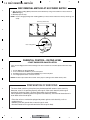
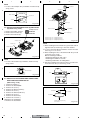
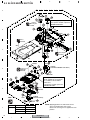
SAFETY INFORMATION
A
This service manual is intended for qualified service technicians ; it is not meant for the casual doit-yourselfer. Qualified technicians have the necessary test equipment and tools, and have been
trainedto properly and safely repair complex products such as those covered by this manual.
Improperly performed repairs can adversely affect the safety and reliability of the product and
may void the warranty. If you are not qualified to perform the repair of this product properly and
safely, you should not risk trying to do so and refer the repair to a qualified service technician.
WARNING !
THE AEL (ACCESSIBLE EMISSION LEVEL) OF THE LASER POWER OUTPUT IS LESS THAN CLASS 1
BUT THE LASER COMPONENT IS CAPABLE OF EMITTING RADIATION EXCEEDING THE LIMIT FOR
CLASS 1.
A SPECIALLY INSTRUCTED PERSON SHOULD DO SERVICING OPERATION OF THE APPARATUS.
B
LASER DIODE CHARACTERISTICS
FOR DVD : MAXIMUM OUTPUT POWER : 5 mW
WAVELENGTH : 650 nm
FOR CD : MAXIMUM OUTPUT POWER : 5 mW
WAVELENGTH : 780 nm
C
LABEL CHECK
Location: inside of the unit
D
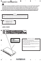
Additional Laser Caution
1.
• Laser diode is driving with Q2303,Q2305(650nm LD) and Q2302,
Q2304(780nm LD)on the DVD MT PCB Assy.
Therefore, when short-circuit between the emitter and collector of these
transistors or the base voltage is supplied for transistors turn on, the
laser oscillates. (failure mode)
• In the test mode ∗ , there is the mode that the laser oscillates except
for the disc judgment and playback. LD ON mode in the test mode
oscillates with the laser forcibly.
(Printed on the Rear Panel)
E
2. When the cover is open, close viewing through the objective lens with
the naked eye will cause exposure to the laser beam.
∗ : See page 29.
ST
AN
ON DB
Y/
OP
EN
/CL
OS
E
TO
P ME
NU
F
HO
MEME
NU
ME
NU
EN
TE
R
RE
TU
RN
2
DV-600AV-S
1
2
3
4
5
6
7
8
[Important Check Points for Good Servicing]
In this manual, procedures that must be performed during repairs are marked with the below symbol.
Please be sure to confirm and follow these procedures.
A
1. Product safety
Please conform to product regulations (such as safety and radiation regulations), and maintain a safe servicing environment by
following the safety instructions described in this manual.
1 Use specified parts for repair.
Use genuine parts. Be sure to use important parts for safety.
2 Do not perform modifications without proper instructions.
Please follow the specified safety methods when modification(addition/change of parts) is required due to interferences such as
radio/TV interference and foreign noise.
3 Make sure the soldering of repaired locations is properly performed.
B
When you solder while repairing, please be sure that there are no cold solder and other debris.
Soldering should be finished with the proper quantity. (Refer to the example)
4 Make sure the screws are tightly fastened.
Please be sure that all screws are fastened, and that there are no loose screws.
5 Make sure each connectors are correctly inserted.
Please be sure that all connectors are inserted, and that there are no imperfect insertion.
6 Make sure the wiring cables are set to their original state.
Please replace the wiring and cables to the original state after repairs.
In addition, be sure that there are no pinched wires, etc.
C
7 Make sure screws and soldering scraps do not remain inside the product.
Please check that neither solder debris nor screws remain inside the product.
8 There should be no semi-broken wires, scratches, melting, etc. on the coating of the power cord.
Damaged power cords may lead to fire accidents, so please be sure that there are no damages.
If you find a damaged power cord, please exchange it with a suitable one.
9 There should be no spark traces or similar marks on the power plug.
When spark traces or similar marks are found on the power supply plug, please check the connection and advise on secure
connections and suitable usage. Please exchange the power cord if necessary.
0 Safe environment should be secured during servicing.
D
When you perform repairs, please pay attention to static electricity, furniture, household articles, etc. in order to prevent injuries.
Please pay attention to your surroundings and repair safely.
2. Adjustments
To keep the original performance of the products, optimum adjustments and confirmation of characteristics within specification.
Adjustments should be performed in accordance with the procedures/instructions described in this manual.
3. Lubricants, Glues, and Replacement parts
Use grease and adhesives that are equal to the specified substance.
Make sure the proper amount is applied.
E
4. Cleaning
For parts that require cleaning, such as optical pickups, tape deck heads, lenses and mirrors used in projection monitors, proper
cleaning should be performed to restore their performances.
5. Shipping mode and Shipping screws
To protect products from damages or failures during transit, the shipping mode should be set or the shipping screws should be
installed before shipment. Please be sure to follow this method especially if it is specified in this manual.
F
3
DV-600AV-S
5
6
7
8
1
2
3
4
CONTENTS
SAFETY INFORMATION ..................................................................................................................................... 2
1. SERVICE PRECAUTIONS ............................................................................................................................... 5
1.1 NOTES ON SOLDERING .......................................................................................................................... 5
1.2 WHEN REPLACING DVD DECK ............................................................................................................... 5
1.3 DISC REMOVAL METHOD........................................................................................................................ 6
2. SPECIFICATIONS ............................................................................................................................................ 7
2.1 ACCESSORIES ......................................................................................................................................... 7
2.2 SPECIFICATIONS...................................................................................................................................... 8
2.3 DISC/CONTENT FORMAT ........................................................................................................................ 9
2.4 PANEL FACILITIES .................................................................................................................................. 11
3. BASIC ITEMS FOR SERVICE........................................................................................................................ 14
3.1 CHECK POINTS AFTER SERVICING..................................................................................................... 14
3.2 PCB LOCATIONS .................................................................................................................................... 15
3.3 JIGS LIST ................................................................................................................................................ 16
4. BLOCK DIAGRAM .......................................................................................................................................... 18
4.1 OVERALL WIRING CONNECTION DIAGRAM........................................................................................ 18
4.2 OVERALL BLOCK DIAGRAM.................................................................................................................. 20
4.3 DVD LOADER BLOCK DIAGRAM ........................................................................................................... 21
4.4 POWER BLOCK DIAGRAM..................................................................................................................... 22
5. DIAGNOSIS .................................................................................................................................................... 23
5.1 TROUBLE SHOOTING ............................................................................................................................ 23
5.2 METHOD FOR DIAGNOSING DEGRADATION OF THE LDS ON THE PICKUP ASSY......................... 28
6. SERVICE MODE ............................................................................................................................................ 29
6.1 SERVICE MODE PROCEDURE.............................................................................................................. 29
6.2 SERVICE MODE IN ................................................................................................................................. 30
6.3 DISPLAY SPECIFICATION OF THE SERVICE MODE............................................................................ 31
6.4 FUNCTIONAL SPECIFICATION OF THE SHORTCUT KEY................................................................... 32
6.5 FUNCTIONAL SPECIFICATION OF THE SERVICE MODE.................................................................... 33
7. DISASSEMBLY ............................................................................................................................................... 34
7.1 EXTERIOR SECTION.............................................................................................................................. 34
7.2 DVD DECK SECTION.............................................................................................................................. 36
8. EACH SETTING AND ADJUSTMENT ........................................................................................................... 40
8.1 ADJUSTMENT ......................................................................................................................................... 40
8.2 RE-WRITE FOR DVD FIRMWARE .......................................................................................................... 40
9. EXPLODED VIEWS AND PARTS LIST .......................................................................................................... 42
9.1 PACKING SECTION ................................................................................................................................ 42
9.2 EXTERIOR SECTION.............................................................................................................................. 44
9.3 06 DVD MECHA SECTION...................................................................................................................... 46
10. SCHEMATIC DIAGRAM ............................................................................................................................... 48
10.1 DVD MT PCB ASSY (1/7) ...................................................................................................................... 48
10.2 DVD MT PCB ASSY(2/7) ....................................................................................................................... 50
10.3 DVD MT PCB ASSY(3/7) ....................................................................................................................... 52
10.4 DVD MT PCB ASSY(4/7) ....................................................................................................................... 54
10.5 DVD MT PCB ASSY(5/7) ....................................................................................................................... 56
10.6 DVD MT PCB ASSY(6/7) ....................................................................................................................... 58
10.7 DVD MT PCB ASSY(7/7) ....................................................................................................................... 60
10.8 OPERATION 1 and OPERATION 2 PCB ASSYS .................................................................................. 62
10.9 POWER PCB ASSY (1/2) ...................................................................................................................... 64
10.10 POWER PCB ASSY (2/2) .................................................................................................................... 66
10.11 USB PCB ASSY................................................................................................................................... 68
10.12 WAVE FORMS ..................................................................................................................................... 70
11. PCB CONNECTION DIAGRAM ................................................................................................................... 72
11.1 DVD MT PCB ASSY............................................................................................................................... 73
11.2 OPERATION 1 PCB and OPERATION 2 PCB ASSYS.......................................................................... 75
11.3 POWER PCB ASSY............................................................................................................................... 76
11.4 USB PCB, LOADING MOTOR and SW ASSYS .................................................................................... 78
12. PCB PARTS LIST ......................................................................................................................................... 79
A
B
C
D
E
F
4
DV-600AV-S
1
2
3
4
5
6
7
8
1. SERVICE PRECAUTIONS
1.1 NOTES ON SOLDERING
NOTES ON SOLDERING
A
• For environmental protection, lead-free solder is used on the printed circuit boards mounted in this unit.
Be sure to use lead-free solder and a soldering iron that can meet specifications for use with lead-free solders for repairs
accompanied by reworking of soldering.
• Compared with conventional eutectic solders, lead-free solders have higher melting points, by approximately 40 ºC.
Therefore, for lead-free soldering, the tip temperature of a soldering iron must be set to around 373 ºC in general, although
the temperature depends on the heat capacity of the PC board on which reworking is required and the weight of the tip of
the soldering iron.
Do NOT use a soldering iron whose tip temperature cannot be controlled.
B
Compared with eutectic solders, lead-free solders have higher bond strengths but slower wetting times and higher melting
temperatures (hard to melt/easy to harden).
The following lead-free solders are available as service parts:
• Parts numbers of lead-free solder:
GYP1006 1.0 in dia.
GYP1007 0.6 in dia.
GYP1008 0.3 in dia.
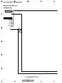
1.2 WHEN REPLACING DVD DECK
C
WHEN REPLACING DVD DECK
[ Removing the DVD Deck ]
Before removing Pick Up PCB and DVD PCB connector, short circuit the position shown in Fig. 1 using
a soldering iron. If you remove the DVD Deck with no soldering, the Laser may be damaged.
[ Installing the DVD Deck ]
Remove all the soldering on the short circuit position after the connection of Pick Up PCB and DVD
PCB connector.
D
NOTE
• Before your operation, please read “PREPARATION OF SERVICING” .
• Use the Lead Free solder.
• Manual soldering conditions
• Soldering temperature: 320 ± 20˚C
• Soldering time: Within 3 seconds
• Soldering combination: Sn-3.0Ag-0.5Cu
• When Soldering/Removing of solder, use the draw in equipment over the Pick Up Unit to prevent the
Flux smoke from it.
E
Short circuit using a
soldering iron.
Pick Up PCB
F
Fig. 1
5
DV-600AV-S
5
6
7
8
1
2
3
4
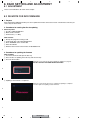
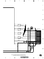
1.3 DISC REMOVAL METHOD
DISC REMOVAL METHOD AT NO POWER SUPPLY
A
1. Slide the Rack Loading (White) toward the arrow direction by using a minus driver to release the lock.
(Refer to Fig. 1)
2. Manually open the Tray.
NOTE: Please strongly pushing Rack Loading (White) to release the lock because the tray doesn't go out
easily.
DVD Player (Bottom Side)
B
Rack Loading (White)
C
Fig. 1
PARENTAL CONTROL - RATING LEVEL
4 DIGIT PASSWORD CANCELLATION
If the stored 4 digit password in the Rating Level menu needs to be cancelled, please follow the steps
below.
D
1.
2.
3.
4.
Set the DVD to the Stand-by Mode.
Press and hold the 'STOP' key on the front panel.
Simultaneously press and hold the POWER key on the front panel.
The 4 digit password has now been cleared.
NOTE: The above procedure will reset ALL of the player's settings to the default factory state.
PREPARATION OF SERVICING
The laser diode used for a pickup head may be destroyed with external static electricity.
Moreover, even if it is operating normally after repair, when static electricity discharge is
received at the time of repair, the life of the product may be shortened.
Please perform the following measure against static electricity, be careful of destruction of a
laser diode at the time of repair.
E
• Place the unit on a workstation equipped to protect against static electricity, such as
conductive mat.
• Soldering iron with ground wire or ceramic type is used.
• A worker needs to use a ground conductive wrist strap for body.
F
6
DV-600AV-S
1
2
3
4
5
6
7
8
2. SPECIFICATIONS
2.1 ACCESSORIES
Accessories
A
• Remote control ×1
(07650NU020)
1
2
3
4
5
6
7
8
9
• Audio / Video cable(1.2m) ×1
(red/white/yellow)
(06CPBA2006)
• Power cable ×1
(1206158802 : WYXZT5, WYXZTUR5)
(1206138802 : WVXZT5)
B
0
• Warranty Card
• Operating Instructions
PLAY MODE SURROUND
ZOOM
DISPLAY
• Dry cell batteries ×2
(AA/R6P)
C
D
E
F
7
DV-600AV-S
5
6
7
8
1
2
3
4
2.2 SPECIFICATIONS
A
General
S-video output
Power requirements
. . . . . . . . . . . . . . . . . AC 220 V to 240 V, 50 Hz/60 Hz
Power consumption
DV-600AV . . . . . . . . . . . . . . . . . . . . . . . . . . . . .12 W
Power consumption (standby. . . . . . . . . . . . . . . . 0.8 W
Weight . . . . . . . . . . . . . . . . . . . . . . . . . . . . . . . . 1.8 kg
Y (luminance) - Output level. . . . . . . . . . .1 Vp-p (75 Ω)
C (color) - Output level . . . . . . . . . . . 286 mVp-p (75 Ω)
Jack . . . . . . . . . . . . . . . . . . . . . . . . . . . . . . . . . S-video
Dimensions
DV-600AV . . . . . . . . . . . . . . . . . . . . . . . . . . . . . .
420 (W) mm x 49.5 (H) mm x 215.5 (D) mm
Operating temperature. . . . . . . . . . . . . +5 ºC to +35 ºC
Operating humidity. . . . . . . . . . . . . . . . . . . 5 % to 85 %
(no condensation)
B
AV Connector (21-pin connector
assignment)
AV connector output. . . . . . . . . . . . . . 21-pin connector
This connector provides the video and audio
signals for connection to a compatible colour TV
or monitor.
Video output
Output level . . . . . . . . . . . . . . . . . . . . . . .1 Vp-p (75 Ω)
Jack. . . . . . . . . . . . . . . . . . . . . . . . . . . . . . . . . . . . RCA
Audio output (1 stereo pair)
Output level . . . . . . . . . . . . . . . . . . During audio output
200 mVrms (1 kHz, –20 dB)
Number of channels. . . . . . . . . . . . . . . . . . . . . . . . . . .2
Jacks . . . . . . . . . . . . . . . . . . . . . . . . . . . . . . . . . . .RCA
HDMI output
HDMI output . . . . . . . . . . . . . . . . . . . . . . . . . . . . .19 pin
Audio output (multi-channel / L, R, C, SW,
SL, SR)
Output level. . . . . . . . . . . . . . . . . . .During audio output
200 mVrms (1 kHz, –20 dB)
Number of channels. . . . . . . . . . . . . . . . . . . . . . . . . . .6
Jacks. . . . . . . . . . . . . . . . . . . . . . . . . . . . . . . .RCA jack
C
PIN no.
1 . . . . . . . . . . . . . . . . . . . . . . . . . . . . . . . Audio 2/R out
3 . . . . . . . . . . . . . . . . . . . . . . . . . . . . . . . Audio 1/L out
4 . . . . . . . . . . . . . . . . . . . . . . . . . . . . . . . . . . . . . . GND
7 . . . . . . . . . . . . . . . . . . . . . . . . . . . . . . . . . . . . . . B out
8 . . . . . . . . . . . . . . . . . . . . . . . . . . . . . . . . . . . . . Status
11 . . . . . . . . . . . . . . . . . . . . . . . . . . . . . . . . . . . . . G out
15 . . . . . . . . . . . . . . . . . . . . . . . . . . . . . . . . . . . . . R out
17 . . . . . . . . . . . . . . . . . . . . . . . . . . . . . . . . . . . . . GND
19 . . . . . . . . . . . . . . . . . . . . . . . . . . . . . . . . . Video out
21 . . . . . . . . . . . . . . . . . . . . . . . . . . . . . . . . . . . . . GND
D
Component video output
Y (luminance) - Output level . . . . . . . . . . 1 Vp-p (75 Ω)
PB (color) - Output level . . . . . . . . . . . .0.7 Vp-p (75 Ω)
PR (color) - Output level . . . . . . . . . . . .0.7 Vp-p (75 Ω)
Jack . . . . . . . . . . . . . . . . . . . . . . . . . . . . . . . . . . . RCA
E
Digital audio characteristics
Frequency response. . . . . . . . . . . . . . . .4 Hz to 44 kHz
S/N ratio . . . . . . . . . . . . . . . . . . . . . . . . . . . . . . .115 dB
Dynamic range . . . . . . . . . . . . . . . . . . . . . . . . . .100 dB
Total harmonic distortion . . . . . . . . . . . . . . . . 0.0023 %
Wow and flutter . . . . . . . . . . . . . .Limit of measurement
(±0.001 % W. PEAK) or lower
Digital output
Coaxial digital output . . . . . . . . . . . . . . . . . . .RCA jack
Optical digital output
. . . . . . . . . . . . . . . . . . . . . . . . . . . . . Optical digital jack
Accessories
Remote control . . . . . . . . . . . . . . . . . . . . . . . . . . . . . . 1
AA/R6P dry cell batteries . . . . . . . . . . . . . . . . . . . . . . 2
Audio/video cable . . . . . . . . . . . . . . . . . . . . . . . . . . . . 1
Power cable . . . . . . . . . . . . . . . . . . . . . . . . . . . . . . . . 1
Warranty card . . . . . . . . . . . . . . . . . . . . . . . . . . . . . . . 1
Operating instructions
The specifications and design of this product are subject
to change without notice, due to improvement.
Published by Pioneer Corporation.
Copyright © 2007 Pioneer Corporation.
All rights reserved.
F
8
DV-600AV-S
1
2
3
4
5
6
7
8
2.3 DISC/CONTENT FORMAT
Disc/content format playback
compatibility
This player is compatible with a wide range of
disc types (media) and formats. Playable discs
will generally feature one of the following logos
on the disc and/or disc packaging. Note
however that some disc types, such as
recordable CD and DVD, may be in an
unplayable formatósee below for further
compatibility information.
Please also note that recordable discs cannot be
recorded using this player.
DVD-Audio DVD-Video DVD-R
Audio CD Video CD
CD-R
DVD-RW
About DualDisc playback
A
A DualDisc is a new two -sided disc, one side
of which contains DVD content video, audio,
etc. while the other side contains non-DVD
content such as digital audio material.
The non-DVD, audio side of the disc is not
compliant with the CD Audio specification and
therefore may not play.
The DVD side of a DualDisc plays in this
product. DVD-Audio content will not play.
For more detailed information on the DualDisc
specification, please refer to the disc
manufacturer or disc retailer.
B
CD-R/-RW compatibility
• Compatible formats: CD-Audio, Video CD/
Super VCD, ISO 9660 CD-ROM*
containing MP3, WMA, MPEG-4 AAC,
JPEG or DivX video/WMV files
* ISO 9660 Level 1 or 2 compliant. CD
physical format: Mode1, Mode2 XA Form1.
Romeo and Joliet file systems are both
compatible with this player.
CD-RW
Super Audio CD
C
• Multi-session playback: No
• Unfinalized disc playback: No
• File structure (may differ): Up to 299
folders on a disc; up to 648 folders and files
(combined) within each folder
Fujicolor CD
• This unit will play DVD+R/+RW discs.
•
•
DVD+R/DVD+RW compatibility
is a trademark of DVD Format/Logo
Licensing Corporation.
is a trademark of Fuji Photo Film Co. Ltd.
• Also compatible with KODAK Picture CD
This player supports the IECís Super VCD
standard. Compared to the Video CD standard,
Super VCD offers superior picture quality, and
allows two stereo soundtracks to be recorded.
Super VCD also supports the widescreen size.
D
Only DVD+R/DVD+RW discs recorded in
'Video Mode (DVD Video Mode)' which have
been finalized, can be played back. However,
some editing made during the recording may
not be played back accurately.
DVD-R/-RW compatibility
• Compatible formats: DVD-Video, Video
Recording (VR)*
* Edit points may not play exactly as edited;
screen may go momentarily blank at edited
points.
E
• Unfinalized playback: No
Super VCD
• MP3/WMA/MPEG-4 AAC/JPEG or DivX
video/WMV file playback on DVD-R/-RW:
No
F
9
DV-600AV-S
5
6
7
8
1
2
3
Compressed audio compatibility
DivX video compatibility
• Official DivX c Ultra Certified product.
• Plays all versions of DivX c video (including
DivX c 6) with enhanced playback of DivX c
• Compatible formats: MPEG-1 Audio Layer
3 (MP3), Windows Media Audio (WMA),
MPEG-4 AAC
• Sampling rates: 32 kHz, 44.1 kHz or 48 kHz
• Bit-rates: Any (128 kbps or higher recommended)
• VBR (variable bit rate) MP3/WMA/MPEG-4
AAC playback: No
• WMA lossless encoding compatible: No
• DRM (Digital Rights Management)
compatible: No (DRM-protected audio
files will not play in this player
A
media files and the DivX c Media Format.
• File extensions: .avi and .divx (these must
be used for the player to recognize DivX
video files). Note that all files with the .avi
extension are recognized as MPEG4, but not
all of these are necessarily DivX video files
and therefore may not be playable on this
player.
• File extensions: .mp3, .wma, .m4a (these
must be used for the player to recognize
MP3, WMA and MPEG-4 AAC files - do not
use for other file types)
B
About WMV
About MPEG-4 AAC
C
Advanced Audio Coding (AAC) is at the core of the
MPEG-4 AAC standard, which incorporates MPEG-2 AAC,
forming the basis of the MPEG-4 audio compression
technology. The file format and extension used depend on
the application used to encode the AAC file. This unit plays
back AAC files encoded by iTunes© bearing the extension
'.m4a'. DRM-protected files will not play, and files encoded
with some versions of iTunes© may not play, or filenames
may display incorrectly.
Apple and iTunes are trademarks of Apple Inc., registered in the U.S. and other countries.
WMV is an acronym for Windows Media Video and
refers to a video compression technology developed by
Microsoft Corporation. WMV content can be encoded
by using Windows Media® Encoder.
This player is compatible with WMV9 files that are
encoded by using the Windows Media® Encoder 9
Series, with .wmv as an extension.
Compatible with size under 720 x 576 pixels/
720 x 480 pixels.
Advanced Profile is not supported.
JPEG file compatibility
• Compatible formats: Baseline JPEG and
EXIF 2.2* still image files up to a resolution
of 3072 x 2048.
* File format used by digital still cameras.
• Progressive JPEG compatible: No
• File extensions: .jpg (must be used for the
player to recognize JPEG files – do not use
for other file types)
WMA (Windows Media™ Audio)
compatibility
D
4
This player can playback Windows Media
Audio content.
WMA is an acronym for Windows Media Audio
and refers to an audio compression
technology developed by Microsoft
Corporation. WMA content can be encoded by
using Windows Media Player for Windows XP,
Windows Media Player 9 or Windows Media
Player 10 series.
Windows Media is a trademark of Microsoft
Corporation.
This product includes technology owned by
Microsoft Corporation and cannot be used or
distributed without a license from Microsoft
Licensing, Inc.
PC-created disc compatibility
Discs recorded using a personal computer
may not be playable in this unit due to the
setting of the application software used to
create the disc. In these particular instances,
check with the software publisher for more
detailed information.
Discs recorded in packet write mode (UDF
format) are not compatible with this player.
Check the DVD-R/-RW or CD-R/-RW software
disc boxes for additional compatibility
information.
E
About DivX video
DivX is a media technology created by DivX, Inc. DivX
media files contain not only video but also include
advanced media features like menus, subtitles, and
alternate audiotracks. This player can play DivX videos
burned on CD-R/-RW/-ROM discs. Keeping the same
terminology as DVD-Video, individual DivX video files are
called ˝Titles˝. When naming files/titles on a CD-R/-RW
disc prior to burning, keep in mind that by default they will
be played in alphabetical order.
F
10
DV-600AV-S
1
2
3
4
5
6
7
8
2.4 PANEL FACILITIES
2.4.1 FRONT PANEL SECTION
Front panel
A
1
3
2
17
16
15 14
13
12 11 10
9
8
7
4
5
6
B
1
STANDBY/ON
Press to switch the player on or into standby.
9
2
Disc tray
10 Press to start or resume playback.
3 TOP MENU
11 Press to pause playback. Press again to
restart.
Displays the ‘top menu’ of a DVD
disc—this varies with the disc.
4
OPEN/CLOSE
Press to open or close the disc tray.
ENTER & cursor buttons
C
12 Press to stop the disc (you can resume playback by pressing (play)).
Selects the current menu option.
5 MENU
Displays a DVD disc menu—this varies with the disc
and may be the same as the ‘top menu’.
6 RETURN
Returns to the previously dis-played menu screen.
13 and • Press and hold for fast reverse/forward
scanning.
• Press to jump to the previous/next
chapter or track.
7 HOME MENU
8 Display
Description of the display.
D
14 HDMI indicator
Lights when this player is recognized by
another HDMl or DVI/HDCP compatible
component.
15 DVD/USB
Press to turn to USB MODE.
Press once again to return to DVD mode.
E
16 USB port (Type A)
Connect USB device
17
Compatible
This mark indicates compatibility with
DVD-RW discs recorded on a DVD recorder
in Video Recording mode.
F
11
DV-600AV-S
5
6
7
8
1
2
3
4
2.4.2 REMOTE CONTROL
Remote control
A
7
HOME MENU
Press to display (or exit) the on-screen
display.
1
14
2
15
8
Use for reverse slow motion playback, frame
reverse and reverse scanning.
3
4
B
1
2
3
4
5
6
7
8
9
16
9
17
Press to start or resume playback.
10
0
chapter or track, then to previous chapters/
tracks.
18
5
11
6
C
7
19
8
20
10
21
Press to pause playback; press again to
restart.
12 PLAY MODE
9
11
PLAY MODE SURROUND
ZOOM
22
DISPLAY
23
24
12
13
Press to display the Play Mode menu. (You
can also get to the Play Mode menu by
pressing HOME MENU and selecting Play
Mode).
Press to jump to the beginning of the current
13 SURROUND
Press to activate/switch off 2V/SRS TruSurround.
D
14
1
Press to switch the player on or into standby.
2
AUDIO
15 ANGLE
Press to select the audio channel or language.
3
Press to open or close the disc tray.
SUBTITLE
Press to change the camera angle during
DVD multi-angle scene playback.
Press to select a subtitle display.
E
4
Number buttons
5
TOP MENU
16 DVD/USB
Press to turn to USB MODE or return to DVD mode.
17 CLEAR
Press to display the top menu of a DVD disc.
6
ENTER & cursor buttons
18 MENU
Use to navigate on-screen displays and
menus. Press ENTER to select an option or
execute a command.
F
Press to clear a numeric entry.
12
Press to display a DVD disc menu, or the Disc
Navigator if a VR format DVD-RW, CD, Video
CD , MP3, WMA or JPEG disc is loaded.
DV-600AV-S
1
2
3
4
5
6
7
8
19 RETURN
A
Press to return to a previous menu screen.
20
Use for forward slow motion playback, frame
advance and forward scanning.
21
Press to jump to the next chapter or track.
22
B
Press to stop the disc (you can resume playback
by pressing (play)).
23 DISPLAY
Press to display information about the disc
playing.
24 ZOOM
Press to change the zoom level.
C
D
E
F
13
DV-600AV-S
5
6
7
8
1
2
3
4
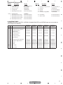
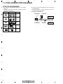
3. BASIC ITEMS FOR SERVICE
3.1 CHECK POINTS AFTER SERVICING
A
Check points after servicing (DVD player)
To keep the product quality after servicing, confirm recommended check points shown below.
No.
B
Check points
1
Confirm the firmware version on Service Mode.
2
Confirm whether the customer complain has been solved. The customer complain must not be reappeared.
Video, audio and operations must be normal.
If the customer complain occurs with the specific disc,
use it for the operation check.
Confirm playback error rates at the innermost and
outermost tracks by using the following disc.
DVD test disc (GGV1025)
The error rates must be less than 5.0e-4.
3
4
Play back a DVD.
(Menu operation, Title/chapter search)
Audio and operations must be normal.
5
Play back a DVD.
(Menu operation, Title/chapter search)
Video, audio and operations must be normal.
Check the appearance of the product.
No scratches or dirt on its appearance after receiving it
for service.
6
C
Procedure
The version of the firmware must be latest.
Update firmware to the latest one, if it is not the latest.
See the table below for the items to be checked regarding video and audio:
Items to be checked regarding video
D
Item to be checked regarding audio
Block noise
Distortion
Horizontal noise
Noise
Dot noise
Volume too low
Disturbed image (video jumpiness)
Volume too high
Too dark
Volume fluctuating
Too bright
Sound interrupted
Mottled color
E
F
14
DV-600AV-S
1
2
3
4
5
6
7
8
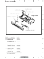
3.2 PCB LOCATIONS
A
POWER PCB ASSY
USB PCB ASSY
DVD MECHA ASSY
OPERATION 3 PCB ASSY
B
DVD MT PCB ASSY
OPERATION 2 PCB ASSY
C
OPERATION 1 PCB ASSY
D
Description
Mark No.
LIST OF ASSEMBLIES
>
Part No.
1..DVD MT PCB ASSY
A2K501A130
1..OPERATION 1 PCB ASSY
(WYXZT5, WVXZT5 types) (*)
A2K501A270
1..OPERATION 1 PCB ASSY
(YXZTUR5 types) (*)
A2K504A270
1..OPERATION 2 PCB ASSY
A2K401A280
1..OPERATION 3 PCB ASSY
A2K401ADF0
1..POWER PCB ASSSY
A2K503A240
1..USB PCB ASSY
A2K401ADD0
1..DVD MECHA ASSY
A2K001A650
E
(*) A2K501A270 and A2K504A270 have same service parts.
But they are NOT COMPATIBLE.
F
15
DV-600AV-S
5
6
7
8
1
2
3
4
3.3 JIGS LIST
7 Jigs list
Name
Service Remote Control Unit
A
Jig No.
GGF1381
Remarks
diagnosis
DVD Test Disc (DVD-Video,NTSC) GGV1025
DVD Test Disc (DVD-Video,PAL) GGV1101
CD Test Disc
STD-905
Operation Check
Operation Check
Operation Check
Lubricants and Glues list
B
Name
Lubricants and Glues No.
Remark
Daifree
GEM1036 (ZLX-ME413A)
Refer to "9.3 06 DVD MECHA SECTION"
Grease
GYA1001 (ZLB-PN397B)
Refer to "9.3 06 DVD MECHA SECTION"
Grease
GEM1018
Refer to "9.3 06 DVD MECHA SECTION"
Cleaning
• Before shipping out the product, be sure to clean the following positions by using the prescribed cleaning tools:
Position to be cleaned
C
Pickup leneses
Cleaning tools
Remark
Cleaning liquid : GEM1004
Cleaning paper : GED-008
D
E
F
16
DV-600AV-S
1
2
3
4
5
6
7
8
A
B
C
D
E
F
17
DV-600AV-S
5
6
7
8
1
2
3
4
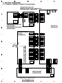
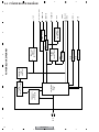
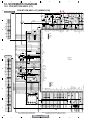
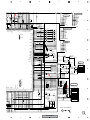
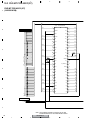
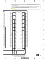
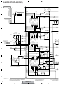
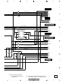
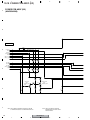
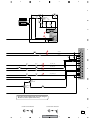
4. BLOCK DIAGRAM
4.1 OVERALL WIRING CONNECTION DIAGRAM
OPERATION 1 PCB ASSY
(WYXZT5, WVXZT5 types : A2K501A270)
(YXZTUR5 types : A2K504A270)
4
3
2
USB
1
1
5
5
USB
V+3E
2
2
4
4
V+3E
LED
3
3
3
3
POWER
4
4
2
2
POWER
SW2
5
5
1
1
SW2
LED
11
1
1
1
10
2
2
2
FLDC+
9
3
3
3
DGND
8
4
4
4
DGND
7
5
5
5
IR
V+3E
6
6
6
6
V+3E
IR
5
7
7
7
DGND
8
8
8
DGND
3
9
9
9
FLDC+
DI (M to F)
2
10
10
10
-28V
CLK
1
11
11
11
FLDC-
CP8102
SPDIF
GND
1
1
G
GND
11
11
2
2
GND
B
10
10
3
3
B
GND
9
9
4
4
GND
R
8
8
5
5
R
RGB-H
7
6
6
RGB-H
7
7
FS
8
8
CVBS
FS
6
7
6
CVBS
5
5
4
4
9
9
GND
3
3
10
10
AUDIO L
GND
2
2
11
11
GND
AUDIO R
1
1
1 2
12
AUDIO R
21
GND
12
12
12
12
FL DC-
FL DC+
13
13
13
13
FL DC+
-28V
14
14
14
14
-28V
CP4004
3
POWER PCB
PCB240
DPF015
NC
3
4
USB_DP
GND
(CD6601)
2
CP6601
1
+5V
(CD6603)
CP6602
USB_DN
USB PCB ASSY
(A2K401ADD0)
NOTE : THE TIMETHIS INTERCONNECTION DIAGRAM IS THE LATEST AT
OF PRINTING AND SUBJECT TO CHANGE WITHOUT NOTICE.
DV-600AV-S
2
3
4
D1-
GND(D)
FL DC-
6
11
D1+
11
D1-S
11
5
11
D2-
P.ON-H
GND(D)
4
AT+3.3V
10
3
9
10
D2+
9
10
D2-S
9
10
4
9
P.ON-H
2
NC
AT+3.3V
CP5901
11
7
8
9
NC
1
AT+3.3V
GND
8
USBN
8
6
8
6
8
6
GND(M)
AT+3.3V
6
7
GND
P.CON+6V
7
6
USBN
6
7
GND
6
7
USBP
6
GND(M)
5
P.CON+6V
5
P.CON+5V
5
5
5
5
USBP
5
USB_FLAG
5
4
GND
P.CON+5V
4
4
4
4
GND
3
4
USB_POWER
18
17
16
15
14
13
12
3
4
3
AT+12V for MUTE
3
GND
2
AT+12V for MUTE 3
3
P.CON+12V
2
2
3
2
2
GND
2
3
1
2
1
1
1
1
NC
10
CP4003
1
P.CON+12V
6
(CD502)
CP502
USB PCB
PCBDD0
DEF133
1
4
CP7301
12
F
18
E
SPDIF
GND
AUDIO L
5
4
4
4
4
GND
2
12
GND
1
3
3
3
3
GND
1
2
G
NC
2
GND
GND
USB+5V
USB+5V
2
2
2
2
P.CON+5V
1
1
1
1
P.CON+5V
1
2
(CD6602)
CP504
1
2
CP503
19
D
E
1
CVBS/Y/U/V
J7302
CP8001
1
1
L
20
1
2
AC INLET
J501
N
21PIN CONNECTOR
J8101
5
DVD MT PC
(A2K501A13
POWER PCB ASSY
(1/2, 2/2)
(A2K503A240)
AC220V-240V_50Hz/60Hz(EU)
CD501_2
6
OPERATION PCB
PCB270
DEF126
OPERATION 2 PCB ASSY
(A2K401A280)
OPERATION 3 PCB ASSY
(A2K401ADF0)
C
2
DO (F to M)
4
B+ 3
S-VIDEO OUT for HE
J7304
STB
H2 H1 H2 H1
E
5
CLK
DI (M to F)
STB
1
GND 2
OPERATION3 PCB
PCBDF0
DEF130
6
-28V
DO (F to M)
B
CP4002
FLDC-
OS651
Vout
(CD601)
CP601
CP604
USB_POWER 1
2
USB_FLAG
(CD604)
CP605
3
1
4
A
5
6
7
8
E
6
1
5
E
3
4
H2 H1 H2 H1
2
E
6
1
5
E
3
4
2
E
LS/RS/C/LFE
J8002
CVBS/Y/U/V
J7302
H2 H1
1
2
2
VCC
H2 H1 H2 H1
GND 3
3
INPUT 1
A
OPTICAL
OS8101
L/R
J8001
CP2301
FOCS RTN
24
24
24
FOCS RTN
FOCS DRV
23
23
23
FOCS DRV
TRKG RTN
22
22
22
TRKG RTN
TRKG DRV
21
21
21
TRKG DRV
NC
20
20
20
NC
GND
GND
19
19
18
18
18
LD_DVD(650)
PD/GND
17
17
17
PD/GND
LD_CD(780)
16
16
16
LD_CD(780)
15
15
15
VR780(CD)
14
14
14
VRCOM
13
13
13
VRCOM
VR650(DVD)
12
12
12
VR650(DVD)
A
11
11
11
A
B
10
10
10
B
VRF(RF_OUT)
9
9
9
VRF(RF_OUT)
SW1(DVD/CD)
8
8
8
SW1(DVD/CD)
C
7
7
7
D
6
6
6
GND
DVD MT PCB ASSY (1/7–7/7)
(A2K501A130)
DVD
DRIVE
DM-4PB
19
LD_DVD(650)
B
GND
VR780(CD)
OPTICAL PICK-UP
C
D
E
5
5
5
E
VCC
4
4
4
VCC
VS
3
3
3
VS
F
2
2
2
F
GND
1
1
1
GND
C
(SW PCB)
SW2
ESE22MH24
CD2301
2H062102
CP2303
SW(GND) 6
6
1
1
LIMIT SW
5
5
2
2
PICK UP INNER LIMIT SWITCH
SLD-
4
4
3
3
3
4
3
4
FEED MOTOR (-)
SLD+
SPD-
2
2
5
5
SPINDLE MOTOR (-)
SPD+
1
1
6
6
GND(SW)
FEED MOTOR (+)
M
M2602
BCZ3B03
M
M2601
JCV9B07
SPINDLE MOTOR (+)
PCB640
DED012
D
(LOADING MOTOR PCB)
SW1
SSS-13-2
CD2302
2H052601
5
SW-2(CLOSE)
3
4
3
SW-1(OPEN)
4
2
5
1
CP2302
CLOSE
1
GND
2
OPEN
LOAD+
LOAD-
GND(SW)
LOADING MOTOR(+)
LOADING MOTOR(-)
M
GND
POWER
HOTPLUG
18
19
SDA
17
NC
SCL
CEC
13
16
CLK12
15
CLK-S
11
14
D0-
8
CLK+
D0+
D0-S
7
9
D16
10
D1+
D1-S
5
D23
4
D2+
D2-S
2
CP5901
1
PCB610
DED003
M2603
BCZ3B52
DVD MECHA ASSY
(A2K001A650)
DVD MT PCB
PCB130
DMF090
E
USB PCB
PCBDD0
DEF133
F
ATTENTION : LES PIECES REPAREES PAR UN > ETANT
DANGEREUSES AN POINT DE VUE SECURITE
N’UTILISER QUE CELLS DECRITES
DANS LA NOMENCLATURE DES PIECES.
CAUTION : SINCE THESE PARTS MARKED BY > ARE
CRITICAL FOR SAFETY,USE ONES
DESCRIBED IN PARTS LIST ONLY
19
DV-600AV-S
5
6
7
8
1
20
2
3
POWER
SUPPLY
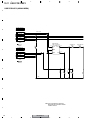
DVD LOADER
(DM4)
DV-600AV-S
4
FLDC+/-
V+5H
-28V
AT+12V for mute
AT+3.3V
+1.8V
P.CON+6V
P.CON+5V
P.CON+12V
16Mbit FLASH
IC4004
ES29LV160EB-70 TG
A0~A20,
AD0~AD7
64Mbit SDRAM
IC4005
HY57V641620ETP-6-C
MA0~MA11,
DQ0~DQ15
ASPDIF
4CH VIDEO DAC
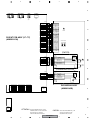
TX0+/-,
TX1+/-,
TX2+/-,
TXC+/-
HDMI
CONNECTOR
CP5901
108MHz
TV Encoder
AMUTE
VIDEO DRIVER 6CH IC
IC7301
LA73054-TLM-E
OPTICAL
COAXIAL
S_VIDEO
4CH BUS SW IC
IC7302
SN74CBT3257PWR
RGB OUT
CVBS OUT
OP
CO
S
V
U
Y
CVBS
21 PIN
L
R
3
AC220V~240V
SERVO
LD_DVD,
LD_CD
MPEG-1/2/
JPEG
VIDEO
DECORDER
AUDIO CODEC/
INTERNAL DAC
IC8002/7/8
AUDIO LPF AND AMP IC
RC4580IDR
B
RF
RF
MPEG/MICON BLOCK
IC4002
MT1389EXE/S-L
DAC_XCSO, SCK, SD,
ACLK, ABCK, ALRCK,
ASDAT0~2
IC8003/4/5
AUDIO DAC IC
PCM1742KE/2K
2
MOTOR DRIVER
IC2301
AM5766
SERVO
FP,STB
E
IR
FIP DRIVER IC
IC651
PT6315
27MHz
SDA, SCL
8K EEPROM
IC4001
S-24CS08AFJ-TB1GE
LFE
C
SL
SR
A
IR RECEIVER (OS651)
ROM-N340TAO
IR
F
KEY
FIP
HNV-08SS44T
RESET IC
IC4003
R3112N291ATR-FA
D
RESET
C
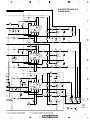
OVERALL BLOCK DIAGRAM
1
4
4.2 OVERALL BLOCK DIAGRAM
5
6
7
D2-
D1+
D1-
D0+
D0-
3
4
6
7
9
16 SDA
15 SCL
19 HOTPLUG
18 POWER
12 CLK-
10 CLK+
D2+
1
2
1
3
4
2
1
L5902
3
4
2
1
TX0-
TX0+
3
4
2
1
L5904
TX1-
TX1+
L5903
TX2+
TX2-
TXC-
TXC+
HDMI_SDA
HDMI_SCL
EEPROM IC
IC4001
S-24CS08AFJ-TB1GE
X4001
27MHz
A
USB_FLAG
USBP
USBN
4
5
USB_POWER
2
1
CP6601
DV-600AV-S
8
P.CON+5V
P.CON+5V
1
2
VIDEO DRIVER 6CH IC
IC7301
LA73054-TLM-E
F
HIGH SIDE SW
IC6601
RT9702-PB
G
GR1~GR8, P1~P16
A
A
IR RECEIVER (OS651)
ROM-N340TAO
IR
21 PIN CTL
BLANKING_OUT
+5V
USB_DN
USB_DN
1
3
2
CP6603
FIP (V651)
HNV-08SS44T
IC8002/7/8
AUDIO LPF AND AMP IC
RC4580IDR
DVD_RGB_H_OUT
Q8104, Q8105
21 PIN CTL
Q8101, Q8102
4CH BUS SW IC
IC7302
SN74CBT3257PWR
IC8003/4/5
AUDIO DAC IC
PCM1742KEG/2K
VSEL1
FIP DRIVER IC
IC651
PT6315
ASPDIF
A
D
SQUEEZE
VSEL1
C
DAC_XCSO, SCK, SD,
ACLK, ABCK, ALRCK,
ASDAT0~2
A, C
FP_DI, FP_DO,
FP_SCK, STB
IR
A, B
SQUEEZE, VSEL1
CVBS
R OUT
G OUT
B OUT
SR
SL
LFE
C
1
OPTICAL
OS8001
1
COAXIAL JACK
J8102
2
3
5
6
LS/RS/S/LFE JACK
J8002
2 R
3 L
L/R JACK
J8001
L
1 R
19
15
11
7
8
16
3
A.......AT+3.3V
B.......+1.8V
C.......P.CON+5V
D.......P.CON+6V
E.......AT+12V
F.......P.CON+12V
G.......-28V
H.......V+5H
OPTICAL
COAXIAL
CVBS
Y
U
V
21PIN CONNECTOR
J8101
6
5
3
2
CVBS/Y/U/V
J7302
3 Y
4 C
S-VIDEO JACK
J7301
7
CP6602
MPEG/MICON IC
IC4002
MT1389EXE/S-L
RESET
RESET IC
IC4003
R3112N291ATR-FA
LETTER, I/XP, S_Y, S_C,
R/CR, B/CB, G/Y, CVBS
6
3
4
L5901
A
A
SDA
SCL
DMSO, FMSO,
TROPEN, TRCLOSE,
TRSO, FOSO,
STBY, V1P4
LDO1, LDO2
MA0~MA11, DQ0~DQ15,
DQM0, DQM1, DBA0, DBA1,
SDCLK, SDCKE, DWE#,
DRAS#, DCAS#, DCS#
A0~A20, AD0~AD7,
PRD#, PCE#, PWR#DCS#
LIMIT, TRIN, TROUT,
OPO, OP+/-
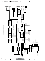
MOTOR DRIVER IC
IC2301
AM5766
D
Q2302~2305
LD DRIVE
A
RF, A, B, C, D, E, F, MDI1
IOA, V20
64Mbit SDRAM
IC4005
HY57V641620ETP-6-C
T+/-, F+/-,
LOAD+/-,
MOT_SLED+/-,
MOT_SPDL+/-
LD_DVD, LD_CD
16Mbit FLASH
IC4004
ES29LV160EB-70TG
C
HDMI CONNECTOR
CP5901
A
SPINDLE/
STEPING/
SLED
MOTOR
OPU
DVD
Loader
(DM-4)
Y OUT
CB OUT
CR OUT
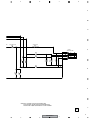
DVD LOADER/MPEG BLOCK DIAGRAM
5
8
4.3 DVD LOADER BLOCK DIAGRAM
A
B
C
D
E
F
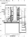
21
F
AC IN
E
22
1
2
3
DV-600AV-S
4
-28V P.CON SW
-28V
FL DC +
FL DC -
AT+3.3V
P.ON-H
V+5H
3
Q502
FL+ P.CON SW
Q504
P.CON SW
HDMI+5V REG IC
IC5902
PQ1K503M2ZPH
P.CON+6V
P.CON+5V
P.CON+12V
AT+12V for mute
+1.8V
2
Q505
6V REG
IC503
PQ070XF01SZH
P.CON +12V SW
Q510
B
P.CON +5V SW
Q515
REG+1.8V
IC4006
LM1117S-ADJ
A
SWITCHING
TRANS
T501
VOLTAGE CTL
IC501
KIA431A-AT
D
POWER CTL
IC502
STR-A6151M
PHOTO COUPLER
IC504
PS2561AL1-1-V (W)
C
POWER BLOCK DIAGRAM
1
4
4.4 POWER BLOCK DIAGRAM
5
6
7
8
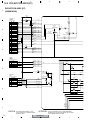
5. DIAGNOSIS
5.1 TROUBLE SHOOTING
A
POWER DOES NOT TURN ON
Is the voltage at
pin 8 and pin 9 of CP502 about 3.3V
and at pin 5 of CP502
about 5V?
No
Check AT+3.3V line of POWER BLOCK.
Check Q515 and peripheral circuit.
B
Yes
Is there waveform at
X4001 about 3.0Vp-p ?
No
Check X4001, IC4001 and
peripheral circuit.
Yes
C
Write DVD FIRMWARE DATA.
DECK DOES NOT ACCEPT
OPEN/CLOSE
D
Is the voltage at
pin 8,19 and 28 of IC2301
about DC6V ?
No
Check P.CON 6V line of
POWER BLOCK.
Yes
E
Is the lose connection
Yes
Check CD2302
connection to DECK.
at CD2302 to DECK ?
No
Change DVD LOADER.
F
23
DV-600AV-S
5
6
7
8
1
A
2
3
4
DOES NOT LIGHT ON DISPLAY
Is the voltage at
pin 13 and pin 43 of IC651
about 3V ?
No
Check AT+3.3V line of
POWER BLOCK.
Yes
B
Replace V651 or IC651.
NO PLAYBACK PICTURE OF AV
JACK
C
Is there
a signal at pin 187 of
IC4002 ?
No
Check IC4002 and
peripheral circuit.
Yes
D
Is there
video signal at pin 33
of IC7301 ?
Yes
Check J7302 and peripheral
circuit.
No
Change IC7301.
E
F
24
DV-600AV-S
1
2
3
4
5
6
7
8
NO DIGITAL AUDIO ON
A
PLAYBACK OF COAXIAL JACK
Is there
waveform at pin 2 of J8102
about 0.3Vp-p?
Check connection at RCA
Yes
Cable.
No
B
Is there
Yes
waveform at pin 215 of IC4002
about 3.3Vp-p ?
Check Q8103 and
peripheral circuit.
No
Change IC4002.
C
NO ANALOG AUDIO ON
PLAYBACK
Is there
AUDIO signal at pins 7 and 8
of IC8003 ?
Yes
D
Check J8001 and peripheral
circuit.
No
Is there
waveform at pins 1,2
and 3 0f IC8003 ?
Yes
Is there
voltage at pin 6 of IC8003
about 5V ?
No
No
Check AT +5V.
E
Yes
Change IC8003.
Change IC4002.
F
25
DV-600AV-S
5
6
7
8
1
2
3
4
NO 5.1CH AUDIO ON
PLAYBACK
A
Yes
Is there
AUDIO signal at pins 7 and 8
of IC8003, IC8004
and IC8005 ?
Check J8001, J8002 and
peripheral circuit.
No
B
Is there
waveform at pins 1,2
and 3 0f IC8003, IC8004
and IC8005 ?
Yes
Is there
voltage at pin 6 of IC8003, IC8004
and IC8005 about 5V ?
No
Check AT +5V.
YES
No
C
Change IC8003, IC8004
and IC8005.
Change IC4002.
THE OUTPUT OF 21PIN DOESN'T
CHANGE (COMPOSITE-RGB)
D
When 21 pin output is RGB,
Is there voltage at pin 16 of
21pin about 4.5V
(No load)?
Check 21pin cable and
Yes
connection.
No
Is the
voltage at pin 188 of IC4002
about 3.3Vp-p ?
E
Yes
Check Q8104, Q8105 and
peripheral circuit.
No
Check IC4002 and
peripheral circuit.
F
26
DV-600AV-S
1
2
3
4
5
6
7
8
Symptoms That May Occur When Any Of The Following ICs Is In Failure
IC
Symptoms
A
EEPROM
User's data cannot be stored in memory.
(DVD MT PCB Assy : IC4001) The ID number is lost.
16M Flash ROM
The power cannot be turned on.
(DVD MT PCB Assy : IC4004) Downloading of the firmware cannot be performed.
DVD IC
Any kind of symptoms (no power, a failure in any of the servo, video and audio systems, etc.) may be
(DVD MT PCB Assy : IC4002) generated, because the DVD processing is performed by a single chip.
64M SDRAM
No power.
(DVD MT PCB Assy : IC4005) Block noise is generated during playback.
B
C
D
E
F
27
DV-600AV-S
5
6
7
8
1
2
3
4
5.2 METHOD FOR DIAGNOSING DEGRADATION OF THE LDS ON THE PICKUP ASSY
Case when this diagnosis is required :
When playback of any disc, including a test disc (DVD: GGV1025, CD: STD-905), cannot be performed
A
How to diagnose
In the case mentioned above, degradation of the laser diodes (LDs) mounted on the PICKUP Assy is suspected.
Measure the voltage between the two ends of one of the resistors mentioned below.
No playback of a DVD :
Measure the voltage between the two ends of R2321 or R2323 on the DVDM
Assy. If the voltage is 0.4 V or higher, the 650-nm LD is degraded.
B
If the measurements show degradation
of an LD, replace the PICKUP Assy.
No playback of a CD :
Measure the voltage between the two ends of R2320 or R2322 on the DVDM
Assy. If the voltage is 0.4 V or higher, the 780-nm LD is degraded.
DVD MT PCB ASSY
W858
C5925
W822
W862
C4064
R4001
R7305
C4068
W856
R4009
C4088
C4080
C5901
C4081
C4082
W827
C4071
W828
B4015
C4072
C4073
W857
C4054
B4018
C7313
C7317
Q7302
W868
R7316
R8089
B4014
R2320
R2323
R2322
R8004
R7317
R8097
C7302
C7330
R7304
C8042
R4067
R4068
C4083
R4066
R4069
R4002
R4061
C4066
C4067
C4110
C7305
R7315
C4074
C4084
C4128
R4006
C4065
R4060
R4053
B4016
R4048
C4061
C4049
C4048
W807
R4065
R4057
C4046
C4014
C4043
W813
C4055
C4051
C4021
C4025
C4012
R4054
R4039
C4020
C4005
C4013
C4019
C4015
C4016
C4033
C4035
C4041
C4036
C4030
C4037
C4001
C4002
C4007
C4027
C4026
C4017
R4020
C4028
R4022
R2318
C2308
C4034
C4003
C4009
C4008
C4105
W821
R4026
R4003
W864
R4064
8004R
R2321
R2327
Q4002
W816
R4005
R4058
W832
R4028
Q4004
C4029
DMF090A
C4038
W804
R4051
C5921
C4052
C4102
C4120
C4101
C4131
C4022
C4040
R4044
R4014
R4004
B4014
C
R8086
W822
R4028
C8051
R8028
SIDE B
E
F
DV-600AV-S
1
2
3
4
R8099
C8006
R8096
Q8021
R8061
C8005
R8066
R8087
R8064
R8059
R8075
C8062
R8065
C8046
C8054
C2302
C4086
W808
C2303
C8055
R8063
R2321
R2320
R2323
R2322
W809
28
B8004
R8084
W832
C4086
C2302
C2303
D
R8083
W804
Q8025
R4058
5
6
7
8
6. SERVICE MODE
6.1 SERVICE MODE PROCEDURE
A
POWER ON
POWER
B
ON
DISC SET
<TRAY OPEN>
<TRAY CLOSE>
OPEN/CLOSE
OPEN/CLOSE
DVD disc
(Player)
(Player)
C
SERVICE MODE: PLAY
CHECK
DVD, CD
<PLAY>
ESC
Press the play key
(
) of the normal
remote control unit.
An address is displayed
TEST
GGF1381
Service mode
remote control
unit
D
DSC - &&&
Notes:
• After going into service mode, if you play back the disc, "DISC-NON" is displayed.
• The video signal and the audio signal are outputted during the servicemode.
• The SKIP key and the SCAN key are effective during the service mode.
E
SERVICE MODE: OFF
ESC
POWER
OR
GGF1381
Service mode
remote control
unit
OFF
F
29
DV-600AV-S
5
6
7
8
1
2
3
4
6.2 SERVICE MODE IN
Service Mode Functional Specification
A
1 Service mode entry
In the power ON state, press the [ESC] (A8-5F) key and [TEST / RANDOM] (A8-5E) key in order of the Service mode remote control
unit.
• Light the all FL and LEDs.
• OSD displays test mode.
Note:
* When pressing the keys of something, the FL displays "NO DISC" and the LED lighting disappears.
2 Release the Service mode
• Turn off the power.
• Press the [ESC] (A8-5F) key of the remote control unit.
B
3 LD ON
DVD : Press the [TEST] (A8-5E) and [1] (A8-01) keys in order, and turn on the laser diode (650n).
CD : Press the [TEST] (A8-5E) and [4] (A8-04) keys in order, and turn on the laser diode (780n).
C
D
E
F
30
DV-600AV-S
1
2
3
4
5
6
7
8
6.3 DISPLAY SPECIFICATION OF THE SERVICE MODE
A
2
Character in bold : Item name
: Information display
3
7
8
9
1
5
6
12
13
14
15
10
11
B
1 Address indication
The address being traced is displayed in number.
(as for the DVD, indication of decimal number is possible.)
DVD : ID indication (hexadecimal number, 8 digits)
[∗ ∗ ∗ ∗ ∗ ∗ ∗ ∗]
CD : ID indication
[∗ ∗ ∗ ∗ ∗ ∗ ∗ ∗]
0 Disc sensing [DSC – ∗ ∗ ∗]
The type of discs loaded is displayed.
[DVD], [CD ], [VCD], [ ]
2 Code indication of remote control unit [R – ∗ ∗ ∗ ∗]
In case of double code, display a 2nd code.
= Version of the FL controller [FL: ∗ ∗ ∗ ∗]
- Jitter value [J – ∗ ∗ ∗ ∗]
Note:Don't use it.
C
~ Region setting of the player [REG: ∗]
Setting value : [1] to [6]
3 Main unit keycode indication [K – ∗ ∗]
5 Tracking status [TRKG – ∗ ∗ ∗]
Tracking on : [ON]
Tracking off : [OFF]
! Destination setting of the FL controller
[MDL: ∗ ∗ ∗ ∗ / ∗ ∗ ∗]
Four characters in the front represent code 01.
Three characters in the back represent the destination code.
J: /J, K: /KU, /KC, /KU/KC, R: /RL/RD, RAM : /RAM,
LB: /LB, WY: /WY
6 Spindle status [SPDL – ∗ ∗ ∗]
[OFF], [CLV]
7 Mechanism (loading) position value [M – ∗ ∗]
Unknown
: [01] or [41]
Open state
: [04]
Close state
: [08]
During opening : [12]
During closing : [22]
D
@ Version of the flash ROM [VERSION: ∗∗∗∗∗∗∗∗]
8 Slider position [S – ∗ ∗ ∗ ∗]
In Side Switch ON : [01]
In Side Switch OFF : [00]
E
9 Output video system [V – ∗ ∗ ∗ ∗]
NTSC system
: [NTSC]
PAL system
: [PAL]
Automatic setting : [AUTO]
Scart terminal output [SK – ∗ ∗]
(Display only the WY model which can do the output setting
of scart terminal.)
VIDEO : [00]
S-VIDEO : [01]
RGB
: [02]
F
31
DV-600AV-S
5
6
7
8
1
2
3
4
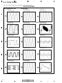
6.4 FUNCTIONAL SPECIFICATION OF THE SHORTCUT KEY
Only during normal playback, the following shortcut keys can be assigned by pressing a required key after pressing the ESC
key of the remote control unit. To quit, press the ESC key
A
Command Contents
Remote Control
Remote
Key Name
Control Code
Conditions
Memory clear and region / revision indication
CLEAR (∗1)
A8-45
Average value measurement of DVD error rate
5 (∗1)
A8-05
CD error rate measurement
5 (∗1)
A8-05
AUDIO
AF-BE
SUBTITLE
AF-36
Scart terminal output : VIDEO
Scart terminal output : S-VIDEO
WY, models equipped with Scart terminal
Scart terminal output : RGB
ANGLE
AF-B5
Progressive OFF
R_SKIP
A3-9D
F_SKIP
A3-9C
ZOOM
AF-37
CHP/TIM (∗1)
A8-13
Only for progressive models
Progressive ON
B
ZOOM ON (X2 -> X4 -> x1)
Service mode indication (error rate indication, etc.)
Model information indication
CHAP (∗1)
A8-40
Title search Input mode IN
Title No. input
Search execution
SIDE A (∗1)
Numbers (∗1)
PLAY (∗1)
A8-4D
A8-00 to A8-09
A8-17
Region confimation mode
A.MON (∗1)
Numbers (∗1)
A8-1E
A8-01 to A8-08
∗1 : Service mode remote control unit
C
• Service mode indication (ESC + CHP/TIM keys)
ID Address
The error rate is always displayed in exponential notation, e.g., ∗.∗ ∗ e - ∗, for both DVDs and CDs.
EDC/ID/AV 1 error history (ID Address, EDC/ID Error, last eight errors)
• Calculation of the average error rate (ESC + "5" [Service mode remote control unit] keys)
The average of the last eight error rates is calculated and indicated in exponential notation. After the calculation is completed, "OK" or "NG" is
displayed. If "NG" is displayed, the disc tray will open (for both DVDs and CDs)
For DVDs: OK with 5.0e-4 or less, for CDs: OK with 7.6e-3 or less
• Indication of model information (ESC + CHAP keys)
The items from 12 to 15 of the SERVICE MODE Indications are displayed. However, in the indications, S in the standard test mode is
changed to CHIP VERSION, and M is changed to FL VERSION.
D
• Region confirmation mode (ESC + A.MON [Service mode remote control unit] + "1"-"8" [Service mode remote control unit] keys)
After you press the A.MON key while holding the ESC key pressed and then input the region number, if the number is different from that set in
the unit, an error message is displayed, and the tray opens.
E
F
32
DV-600AV-S
1
2
3
4
5
6
7
8
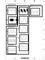
6.5 FUNCTIONAL SPECIFICATION OF THE SERVICE MODE
• Display during Service Mode
To enter Service Mode, press the CHP/TIM key while holding the ESC key pressed.
To quit, press the ESC key.
A
Service mode display
1 ID Address
2 Error rate (always displayed), in exponential notation
ERROR RATE : ∗ ∗ ∗ ∗ ∗ ∗ ∗
(∗∗∗∗)
Number of error
• Calculation of the average error rate
For DVDs: OK with 5.0e-4 or less, for CDs: OK with 7.6e-3 or less
B
ex) For DVDs
• Step 1
• Step 2
%%e -&
%%e -6
%%e -5
%%e -4
%%e -3
%%e -2
%%e -4
: OK
: OK
: Refer to Step 2
: NG
: NG
3.0e -4
4.0e -4
5.0e -4
6.0e -4
7.0e -4
: OK
: OK
: OK
: NG
: NG
C
3 EDC/ID error history (ID Address, EDC/ID errors, last eight errors)
Note:
∗ Error of AV1 is not supported in this player.
Indication plan contents
3
1
2
D
Character in bold : Item name
: Information display
E
F
33
DV-600AV-S
5
6
7
8
1
2
3
4
7. DISASSEMBLY
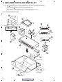
7.1 EXTERIOR SECTION
A
1. REMOVAL OF MECHANICAL PARTS
AND P.C. BOARDS
1-1: TOP CABINET/FRONT CABINET/OPERATION PCB/
OPERATION 2 PCB AND OPERATION 3 PCB
(Refer to Fig. 1-1)
B
1.
2.
3.
4.
5.
6.
7.
1-3: POWER PCB (Refer to Fig. 1-3)
1. Disconnect the following connectors:
(CP502 and CP503).
2. Remove the 2 screws 1.
3. Remove the 4 screws 2.
4. Remove the Power PCB in the direction of arrow.
Remove the 5 screws 1.
Remove the Top Cabinet in the direction of arrow (A).
Disconnect the following connector: (CP4002).
Unlock the 4 supports 2.
Remove the Front Cabinet in the direction of arrow (B).
Remove the 12 screws 3
Remove the Operation PCB/Operation 2 PCB an
Operation 3 PCB in the direction of arrow (C).
2
2
2
2
Power PCB
1
1
Top Cabinet
1
1
1
Operation 3 PCB
1
Operation 2 PCB
Fig. 1-3
(A)
3
C
3
2
1
1-4: DVD DECK (Refer to Fig. 1-4)
(B)
3
(C)
33
2
3
3
3
(C)
Front Cabinet
2
3
3
2
Operation PCB
Fig. 1-1
1. Short circuit the position shown in Fig. 1-4 using a
soldering iron. If you remove the DVD Deck with no
soldering, the Laser may be damaged.
2. Disconnect the following connectors:
(CP2301, CP2302 and CP2303).
3. Remove the 4 screws 1.
4. Remove the DVD Deck in the direction of arrow.
1-2: USB PCB (Refer to Fig. 1-2)
D
Short circuit using a
soldering iron.
1. Disconnect the following connectors:
(CP6601 and CP6602).
2. Remove the 2 screws 1.
3. Remove the USB PCB in the direction of arrow.
1
1
1
DVD Deck
1
1 1
Pick Up PCB
USB PCB
E
Fig. 1-4
Fig. 1-2
F
34
DV-600AV-S
1
2
3
4
5
6
7
8
NOTE
1. Before your operation, please read "PREPARATION OF
SERVICING".
2. Use the Lead Free solder.
3. Manual soldering conditions
• Soldering temperature: 320 ± 20˚C
• Soldering time: Within 3 seconds
• Soldering combination: Sn-3.0Ag-0.5Cu
4. When Soldering/Removing of solder, use the drawing
equipment over the Pick Up Unit to keep the Flux smoke
away from it.
5. When installing the DVD Deck, remove all the soldering
on the short circuit position after the connection of Pick Up
PCB and DVD MT PCB connector.
A
1-5: DVD MT PCB (Refer to Fig. 1-5)
B
1. Remove the 4 screws 1.
2. Remove the 4 screws 2.
3. Remove the DVD MT PCB in the direction of arrow.
2
2
2
DVD MT PCB
2
1
C
11
1
Fig. 1-5
D
E
F
35
DV-600AV-S
5
6
7
8
1
2
3
4
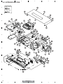
7.2 DVD DECK SECTION
A
2. REMOVAL OF DVD DECK PARTS
NOTE
NOTE
1. In case of the Traverse Ass'y, install it from (1) to (4) in
order. (Refer to Fig. 2-2-B)
2. In case of the Traverse Ass'y installation, hook the wire
on the Loader Ass'y as shown Fig. 2-2-C.
1. Disassemble only the DVD DECK PARTS parts listed
here. Minute adjustments are needed if the disassembly
is done. If the repair is needed except listed parts,
replace the DVD MECHA ASS'Y.
Loader Ass'y (Bottom Side)
2-1: TRAY (Refer to Fig. 2-1-A)
1. Set the Tray opened. (Refer to the DISC REMOVAL
METHOD AT NO POWER SUPPLY)
2. Unlock the 2 supports 1 and draw it while sagging the
Tray.
Rack Loading
Holder Traverse
Loader Ass'y
B
Push to Sag
1
Traverse Ass'y
Tray
Push to Sag
Fig. 2-1-A
C
Check Lock
Fig. 2-2-B
NOTE
Loader Ass'y
1. In case of the Tray installation, install them as the circled
section of Fig. 2-1-B so that the each markers are met.
Loader Ass'y
Check Hook
Fig. 2-2-C
2-3: LOADING MOTOR PCB ASS'Y/ LOADING BELT
(Refer to Fig. 2-3-A)
D
Tray
Fig. 2-1-B
2-2: TRAVERSE ASS'Y (Refer to Fig. 2-2-A)
1.
2.
3.
4.
Remove the screw 1.
Unlock the 2 supports 2.
Remove the Insulator (R) from the Loader Sub Ass'y.
Remove the Traverse Ass'y.
1.
2.
3.
4.
5.
6.
Remove the Loading Belt.
Remove the screw 1.
Remove the Loading Motor PCB Ass'y.
Remove the 2 screws 2.
Remove the Loading Motor.
Remove the Gear Pulley.
Loading Belt
2
2
1
2
E
Loading Sub Ass'y
2
Loader Sub Ass'y
Gear Pulley
Loading Motor
Insulator (R)
Loading Motor PCB Ass’y
1
Traverse Ass'y
• Screw Torque: 2.5 ± 0.3kgf•cm (Screw 1)
• Screw Torque: 1.0 ± 0.3kgf•cm (Screw 2)
• Screw Torque: 2.0 ± 0.3kgf•cm
Fig. 2-3-A
Fig. 2-2-A
F
36
DV-600AV-S
1
2
3
4
5
6
7
NOTE
1. In case of the Pulley Motor installation, check if the value
of the Fig. 2-3-B is correct.
2. When installing the wire of the Loading Motor PCB Ass'y,
install it correctly as Fig. 2-3-C.
Manual soldering conditions
• Soldering temperature: 320 ± 20˚C
• Soldering time: Within 3 seconds
• Soldering combination: Sn-3.0Ag-0.5Cu
3. When installing the Loading Motor PCB Ass'y, install it
correctly as Fig. 2-3-D.
4. In case of the Loading Motor PCB Ass'y installation, hook
the wire on the Loader Sub Ass'y as shown Fig. 2-3-E.
8
2-4: RACK LOADING/MAIN GEAR/PULLEY GEAR
(Refer to Fig. 2-4-A)
1. Unlock the support 2 and remove the Gear Pulley.
2. Remove the Gear Main.
3. Press down the catcher 1 and slide the Rack Loading.
Gear Pulley
A
Rack Loading
Gear Main
Loader Sub Ass’y
2
1
Fig. 2-4-A
Pulley Motor
B
7.0 ± 0.1mm
NOTE
Loading Motor
Safety surface for pressing
of the insert.
Fig. 2-3-B
1. In case of the Rack Loading installation, hook the Rack
Loading on the Loader Sub Ass'y as shown Fig. 2-4-B.
2. When installing the Gear Main, take care the direction of
up or down as shown Fig. 2-4-C.
Rack Loading
BROWN (1)
WHITE (2)
C
Loader Sub Ass'y (Bottom Side)
Check Hook
Loading Motor PCB Ass’y
Fig. 2-3-C
Fig. 2-4-B
Rack Loading
Up Side
Main Gear
D
Down Side
Fig. 2-4-C
2-5: CLAMPER ASS'Y (Refer to Fig. 2-5-A)
A
B
The Lever should be position
between A and B.
Check Hook
Fig. 2-3-D
1. Press the Clamper and rotate the Plate Clamper
clockwise, then unlock the 3 supports 1.
2. Remove the Plate Clamper, Magnet Clamper and
Clamper.
Check Hook
Plate Clamper
E
Magnet Clamper
Main Frame
Loading Motor PCB Ass’y
Check Hook
1
Fig. 2-3-E
1
1
Clamper
Fig. 2-5-A
F
37
DV-600AV-S
5
6
7
8
1
2
3
4
NOTE
1. In case of the Clamper Ass'y installation, install correctly
as Fig. 2-5-B.
Feed Motor
Gear Motor
A
Plate Clamper
Check Lock
5
1
Clamper
Traverse Ass'y
5
Gear Feed
Fig. 2-5-B
4
B
2-6: HOLDER TRAVERSE/INSULATOR (F)/INSULATOR
(R) (Refer to Fig. 2-6-A)
Pickup leneses
1. Remove the Holder Traverse.
GEM1004
2. Remove the 2 Insulator (F).
GED-008
3. Remove the Insulator (R).
Rack Feed Ass'y
Gear Middle
2
Switch PCB Ass'y
3
• Screw Torque: 1.3 ± 0.3kgf•cm (Screw 2)
• Screw Torque: 3.0 ± 0.3kgf•cm (Screw 3)
• Screw Torque: 1.0 ± 0.3kgf•cm (Screw 4, 5)
Insulator (R)
Fig. 2-7-A
Traverse Ass'y
NOTE
Insulator (F)
Holder Traverse
C
Insulator (F)
Fig. 2-6-A
NOTE
1. In case of the Insulator (F) installation, install correctly
as Fig. 2-6-B.
1. When installing the Rack Feed Ass'y, push both ends to
align the teeth as shown Fig. 2-7-B. Then install it.
2. In case of the Gear Motor installation, check if the value
of the Fig. 2-7-C is correct.
3. When installing the wire of the Switch PCB Ass'y, install
it correctly as Fig. 2-7-D.
Manual soldering conditions
• Soldering temperature: 320 ± 20˚C
• Soldering time: Within 3 seconds
• Soldering combination: Sn-3.0Ag-0.5Cu
4. After the assembly of the Traverse Ass'y, hook the wire
on the Traverse Ass'y as shown Fig. 2-7-E.
Insulator (F)
Rack Feed Ass'y
D
Traverse Holder
Push
Push
Fig. 2-6-B
[OK]
2-7: SWITCH PCB ASS'Y/GEAR MIDDLE/GEAR FEED/
RACK FEED ASS'Y/FEED MOTOR
(Refer to Fig. 2-7-A)
E
[NG]
Fig. 2-7-B
1. Unlock the support 1.
2. Remove the Gear Middle.
3. Remove the screw 2.
4. Remove the Rack Feed Ass'y.
5. Remove the screw 3.
6. Remove the Switch PCB Ass'y.
7. Remove the screw 4.
8. Remove the Gear Feed.
9. Remove the 2 screws 5.
10. Remove the Feed Motor.
11. Remove the Gear Motor.
Gear Motor
8.0 ± 0.2mm
Feed Motor
Safety surface for pressing
of the insert.
Fig. 2-7-C
F
38
DV-600AV-S
1
2
3
4
5
6
Switch PCB Ass'y
7
8
~ FEED MOTOR ~
A
WHITE (4)
BROWN (3)
~ SPINDLE MOTOR ~
YELLOW (2)
GREEN (1)
Fig. 2-7-D
B
Traverse Ass'y
Check Hook
• Loosen the wire in the direcion of the arrow.
Fig. 2-7-E
C
2-8: FFC WIRE HANDLING
1. When installing the FFC, fold it correctly and install it as
shown from Fig. 2-8.
NOTE
1. Do not make the folding lines except the specified
positions for the FFC.
[ 24 pin FFC ]
Fold
Printing Surface
D
79 ± 1 mm
Reinforcement Plate
To Pick Up PCB
Fig. 2-8
E
F
39
DV-600AV-S
5
6
7
8
1
2
3
4
8. EACH SETTING AND ADJUSTMENT
8.1 ADJUSTMENT
A
There is no information to be shown in this chapter.
8.2 RE-WRITE FOR DVD FIRMWARE
1. Purpose
After replacing the DVD MT PCB Assy, be sure to update the firmware to the latest version. The firmware of the Assy for
service may not be the latest.
2. Procedures for creating the disc for updating
B
Necessary tools:
1 PC with a CD-R/CD-RW drive
2 Blank CD-R or CD-RW
3 Firmware file (∗∗∗∗∗.BIN)
How to create:
1 Start up the program for writing to CD.
2 Load a blank disc in the CD-R/CD-RW drive.
3 Enter "PIONEER" as the volume label.
4 Select the .BIN file.
5 Write the latest version of the firmware in ISO 9660 format.
C
3. Procedures for updating the firmware
How to update:
1 Turn on the main unit and open the disc tray.
2 Place the disc for updating in the disc tray and close the tray.
3 Press the PLAY button.
While the screen shown at left is being displayed, updating is in progress.
DO NOT TURN OFF THE POWER DURING UPDATING.
D
4 Updating of the firmware is completed.
When the screen with the Pioneer logo is displayed, updating is completed.
The time required for updating is about 2 minutes.
E
F
40
DV-600AV-S
1
2
3
4
5
6
7
8
4. How to confirm the version of the firmware
Press the ESC then the CHAP key on the remote control unit for servicing. The version of the firmware is labeled ROM
NUMBER. Check if the version is the latest one.
A
AREA:WY
REGION:2
ROM NUMBER
YGA6B23A
REG CHK
40
SUM CHK
02A5
FL VERSION
1.16
CHIP VERSION
1389FE
B
How to interpret the version code:
YGA6B23A
Number of releases on the same release date
Release date:
6: Year
B: Month (1-9 [Jan-Sep], A-C [Oct-Dec])
23: Day
C
Fixed
5. Troubleshooting
1 If updating of the firmware failed
If the main unit was turned off during updating, it cannot initialize and start up again properly. In such a case, replace the
flash ROM on the DVD MT PCB Assy.
2 If updating of the firmware using the disc for updating failed
• Was the disc for updating recognized properly?
Check if the volume label of the disc is PIONEER.
• Is playback of a disc other than the disc for updating possible?
If playback of a test CD is also impossible, a reading section, such as PU, may be defective. In such a case, repair the
defective part first.
If playback of a test CD is possible, the disc for updating may be defective. Check for any scratches or foreign matter,
such as fingerprints, on the reading surface.
If no problem is found with the disc, create a new disc for updating again.
D
E
F
41
DV-600AV-S
5
6
7
8
1
2
3
4
9. EXPLODED VIEWS AND PARTS LIST
NOTES:
A
Parts marked by "NSP" are generally unavailable because they are not in our Master Spare Parts List.
The
mark found on some component parts indicates the importance of the safety factor of the part.
Therefore, when replacing, be sure to use parts of identical designation.
Screws adjacent to mark on product are used for disassembly.
For the applying amount of lubricants or glue, follow the instructions in this manual.
(In the case of no amount instructions, apply as you think it appropriate.)
9.1 PACKING SECTION
B
YXZTUR5 Only
Except
WVXZT5
C
WVXZT5
Only
D
YXZTUR5 Only
E
YXZTUR5 Only
YXZTUR5 Only
F
42
DV-600AV-S
1
2
3
4
5
6
7
8
PACKING SECTION parts List
Mark No.
>
1
2
3
4
5
NSP 6
7
8
9
10
Description
Mark No.
Part No.
Power Cable
Audio/Video Cable
Remote Control
Package Pad
Operating Instructions (E)
See Contrast table (2)
06CPBA2006
07650NU020
792WHAA237
See Contrast table (2)
Warranty Card
Operating Instructions (E/I)
Operating Instructions (G/F)
Operating Instructions (S/D)
Operating Instructions (R)
J2K00102A
See Contrast table (2)
See Contrast table (2)
See Contrast table (2)
See Contrast table (2)
Description
Part No.
11
12
13
14
15
Polyethylene Bag,Instruction
Gift Sheet
Package
Gift Box
Polyethylene Bag,INSTA5
See Contrast table (2)
791WHAA183
See Contrast table (2)
See Contrast table (2)
791WHAA040
16
17
Label Safety
Caution Label
See Contrast table (2)
See Contrast table (2)
B
(2) CONTRAST TABLE
DV-600AV-S/WYXZT5, /WVXZT5, /YXZTUR5, DV-600AV-K/WYXZT5 and YXZTUR5 types are constructed the
same except for the following :
Mark No.
>
1
5
7
8
9
10
11
13
14
NSP 16
Symbol and Description
Power Cable
Operating Instructions (English)
Operating Instructions
(English, Italian)
Operating Instructions
(German, French)
Operating Instructions
(Spanish, Duch)
Operating Instructions (Russian)
Polyethylene Bag,Instruction
Package
Gift Box
Label Safety
17 Carton Label
DV-600AV-S/
WYXZT5
DV-600AV-S/
WVXZT5
DV-600AV-S/
YXZTUR5
DV-600AV-K/
WYXZT5
DV-600AV-K/
YXZTUR5
1206158802
Not used
J2K40121B
1206138802
J2K40601B
Not used
1206158802
Not used
Not used
1206158802
Not used
J2K40121B
1206158802
Not used
Not used
J2K40122B
Not used
Not used
J2K40122B
Not used
J2K40123B
Not used
Not used
J2K40123B
Not used
Not used
Not used
J2K40801B
Not used
JB5KD400
JB5KD200
JB5KD200
JB5KD400
792WHAA227 792WHAA232 792WHAA227 792WHAA227
793WCDD419 793WCDD518 793WCDD419 793WCDD508
Not used
Not used
723000D306
Not used
Not used
Not used
723000D600
Not used
A
C
J2K40801B
JB5KD200
792WHAA227
793WCDD508
723000D306
723000D594
D
E
F
43
DV-600AV-S
5
6
7
8
1
2
3
4
9.2 EXTERIOR SECTION
NON-CONTACT
SIDE
A
CONTACT SIDE
B
A
C
E
C
C
E
A
D
B
B
D
D
E
F
44
DV-600AV-S
1
2
3
4
5
6
7
8
EXTERIOR SECTION parts List
Mark No.
>
1
2
3
4
5
Description
Mark No.
Part No.
DVD MT PCB Assy
OPERATION 1 PCB Assy
OPERATION 2 PCB Assy
OPERATION 3 PCB Assy
POWER PCB Assy
A2K501A130
See Contrast table (2)
A2K401A280
A2K401ADF0
A2K503A240
USB PCB Assy
DVD MECHA ASSY
Shield,21Pin
Plate,Bottom
Sheet,Caution
A2K401ADD0
A2K001A650
761WSA0237
702WSAA201
726000A140
11
12
13
14
15
Plate,Cover power
Holder,FFC
Cushion,Leg
Cabinet,Top
Spring Earth
755WPAA031
761WPA0396
VEB1349
See Contrast table (2)
743WKAA015
16
17
18
19
20
Cushion (15x20x16)
Screw,Tap Tite(S)-Bind Wash.
Screw,Tap Tite(S) (3x5.5)
Screw,Tap Tite(B) (3x6.0)
Screw,Tap Tite(B)Pan (3x6)
8965TS101B
816423063U
8107D3055U
See Contrast table (2)
810913060U
6
7
8
NSP 9
NSP 10
21
22
NSP 23
NSP 24
NSP 25
Description
Part No.
Screw,Tap Tite(P) (2.6x8)
Screw,Tap Tite(P) Bind WH7
Sheet,Jack 1
Sheet,Jack 2
Sheet,Jack 3
811022680U
8110I2680U
722631A185
See Contrast table (2)
See Contrast table (2)
Sheet DVD
Front Cabi Assy
Flap, DVD
Spring, Flap-DVD
Cord Connector (CD502)
7236740001
See Contrast table (2)
712WPAA150
743WKA0052
06CU2E3301
31
32
33
34
NSP 35
Cord Jumper (CD601)
Cord Jumper (CD7301)
Cord Jumper (CD604)
Cord Jumper (CD6601)
Angle PCB
122H0B1003
122H0C3002
122H051204
122H063401
761WSAA076
36
NSP 37
38
Screw Pan
Sheet Caution
Spring Earth
810213060U
725000A094
753WUAA012
26
27
28
29
30
A
B
C
(2) CONTRAST TABLE
DV-600AV-S/WYXZT5, /WVXZT5, /YXZTUR5, DV-600AV-K/WYXZT5 and /YXZTUR5 types are constructed the
same except for the following :
Mark No.
NSP
NSP
Symbol and Description
DV-600AV-S/
WYXZT5
DV-600AV-S/
WVXZT5
DV-600AV-S/
YXZTUR5
DV-600AV-K/
WYXZT5
DV-600AV-K/
YXZTUR5
2
13
19
24
25
OPERATION 1 PCB Assy
Cabinet, Top
Screw,Tap Tite(B) (3x6.0)
Sheet, Jack 2
Sheet, Jack 3
A2K501A270
702WSB0114
8109K3060U
722631A186
722631A199
A2K501A270
702WSB0114
8109K3060U
722631A186
722631A199
A2K504A270
702WSB0114
8109K3060U
722631A186
722631A255
A2K501A270
702WSB0115
8109K3060S
722631A251
722631A252
A2K408A270
702WSB0115
8109K3060S
722631A251
722631A260
27
Front Cabi Assy
7A701A898A
7A701A898A
7A701A898A
7A701A947A
7A701A947A
D
E
F
45
DV-600AV-S
5
6
7
8
1
2
3
4
9.3 06 DVD MECHA SECTION
A
Cannot supply separately.
If the repair is needed, replace the
LOADER SUB ASS'Y.
AB
Lubricating Oil
GYA1001
B
AB
Daifree
GEM1036
AB
AB
AC
AB
AB
C
AB
Lubricating Oil
GYA1001
AC
SW1
CD2001
PCB610
(LOADING MOTOR PCB ASS'Y)
Pickup leneses
GEM1004
GED-008
D
CD2302
Do not replace the parts. Because,
minute adjustments are needed if
this condition is disassembled
further more.
If the repair is needed, replace the
DVD MECHA ASS'Y.
AA
Grease
GEM1018
E
Note :
PCB640
(SW PCB ASS'Y)
SW2
CD2301
F
CLASS
PART NO.
GREASE
GEM1018
AA
GYA1001
AB
GEM1036
AC
NOTE: Applying positions AA, AB and AC for the
grease are displayed for this section.
Check if the correct grease is applied for each
position.
MARK
46
DV-600AV-S
1
2
3
4
5
6
7
8
06 DVD MECHA SECTION parts List
Mark No.
Description
Part No.
1
2
3
4
5
••••••
Gear,Middle
Loading Motor
Pulley,Motor
FEED Motor
92P100117A
1515S98004
92P100097A
1515S98004
6
7
8
9
10
Cord Jumper (24P)(CD2001)
Cord Jumper (CD2302)
Insulator (F)
Belt,Loading
Insulator (R)
122J4O2202
122H051602
92P200013A
92P200015A
92P200016A
11
12
13
14
15
Frame,main
Tray (R)
Holder ,Traverse
Gear,Pulley
Gear,Main
92P100119A
92P100151A
92P100125A
92P100123A
92P100124A
16
17
18
19
20
Gear,Feed
••••••
Plate, Clamper
LOADER SUB ASSY (R)
Clamper
92P100116A
A
B
92P000023A
92AAA0024A
92P100122A
C
21
22
23
24
25
Screw,Pan (M1.7x3 P3)
Screw,Pan (M1.7x2.3 P3)
Rack,Loading
Gear,Motor
Feed Rack Assy
814011730U
814011723U
92P100121A
92P100088A
92AAA0017A
26
27
28
29
30
Screw,T-Tite(B) (M1.7x5.0 P3)
Screw,Gear Feed
Cord Jumper (CD2301)
Switch (SW1)
Push Switch (SW2)
813381750U
92P700007A
122H061605
0515S32003
0500101036
31
32
33
Screw,Tap Tite(P) (2.6x8)
Sems.Tap Tite(P) (2x8)
Screw (Bind 2x8)
811022680U
816112080U
811022080U
D
E
F
47
DV-600AV-S
5
6
7
8
1
2
3
4
10. SCHEMATIC DIAGRAM
10.1 DVD MT PCB ASSY (1/7)
NC NC
0 0 0 0 0 0.9 3.2 1.6
10
R4030
TP4090
0
RFRPAC
RFRPDC
RFVDD3
ADCVSS
ADCVDD3
LPFOP
LPFIN
LPFIP
LPFON
PLLVDD3
PLLVSS
JITFN
JITFO
XTALI
XTALO
RFVDD18
RFGND18
SADCVSS18
SADCVDD18
ADACVDD3
ADACVSS3
CH7
CH8
ADACVDD1
ADACVDD2
CENTER
ALS
AL
AVCM
AR
ARS
LFE
ADACVSS1
ADACVSS2
APLLVSS
APLLCAP
APLLVDD
SPDIF/GPIO23
GPIO12
GPIO11
DVDD18
GPIO10
256 OSP
MPEG/MICON IC
IC4002
MT1389EXE/S-L
65 DVDD33
66 XIOWR
67 A16
68 HIGHA7
72 73 74 75 76 77 78 79 80 81 82 83 84 85 86 87 88 89 90 91 92 93 94 95 96 97 98 99 100 101 102 103 104 105 106 107 108 109 11
TP4044
R4035
TP4034
0 3.3 3.2 2.8
NC NC
33
UWR#
URD#
0 0 1.8 1.7 3.2 3.2 3.2 3.2 3.2 3.1 3.2 3.2 3.2 3.2 3.2 3.2 3.2
TP4033
0 0.7 1.3
TP4032
0 1.1 1.1 1.4 1.9 0.7
TP4024
TP4025
TP4026
TP4027
TP4028
TP4029
TP4030
TP4031
TP4022
TP4023
0 0.7 0.8 0.8 1.4 1.5
R4001 10K
B
B
100P CH
NR4001
4D03WGJ
0330T5E
RXD
TXD
C4131
A17
A0
AD7
PWR#
A16
A15
A14
A13
A12
A11
A10
A9
A20
PCE#
A1
PRD#
AD0
AD1
IOCE#
AD2
AD3
AD4
AD5
AD6
B4010
STB
FP_DO
SCL
SDA
C4055
0.1
MMZ1608
R102CT
0.1
FP_DI
FP_SCK
MMZ1608R102CT
TP4103
NOTE : THIS SCHEMATIC DIAGRAM IS THE LATEST AT THE TIME
OF PRINTING AND SUBJECT TO CHANGE WITHOUT NOTICE.
3
4
IR
C4025
B4018
IOWR#
2
NC NC
0 0 1.7
255 RFGND
DV-600AV-S
1
C4084 0.1 B
B
0 0 1.6 1.6 1.6
C4024
0.0015
(2125)
C4063
10
0 0 0 3.3 3.3
254 CRTPLP
TP4014
V+1R8
48
0.0
B
B
(2125)
C4061
4.7 B
0 0 1.7 3.3
TP4109
NOTE : THE DC VOLTAGE EACH PART WAS MEASURED
WITH THE DIGITAL TESTER DURING PLAYBACK.
ASPDIF
ABCK
TP4041
ALRCK
R4043 33 TP4043
ASDAT0
R4040 33
ASDAT1
R4038
TP4037
ASDAT2
TP4036
33
ADAC_GND
W807
B4014 V+3
C4023
6.3V
470 YK_P MMZ1608R102CT
W830
R4027 100
B
B
C4042
0.047
C4044
0.047
R4050 33
C4049
12P CH
B
C4048
C4043
0.1
B
B
0.1
C4041
0.1
C4034
20P CH
C4035
C4032 0.1 B
10K
C
16
Y
C4
253 HRZFC
TP4015
TP4016
TP4017
TP4018
TP4019
TP4020
TP4021
3.3V
B
C4022
R4048 10K
R4053
C4051
0.0
0 0 0.8 1.3 1.1 1.7
0.1
3.3
SDA
4
OSN
RFGC
IREF
AVDD3
AGND
DVDA
DVDB
DVDC
DVDD
DVDRFIP
MA
MB
MC
MD
SA
SB
SC/TNI
SD/TPI
MDI1
MDI2
LDO2
LDO1
SVDD3
CSO/RFOP
RFLVL/RFON
SGND
V2REF
V20
VFEFO
EFO
TEO
TEZISLV
OP_OUT
OP_INN
OP_INP
DMO
FMO
TROPENPWM
PWMOUT1/_ADIN0
TRO
FOO
AGND18_DMPLL
AVDD18_DMPLL
USB_DP
USB_DM
VDD33_USB
VSS33_USB
PAD_VRT
VDD18_USB
VSS18_USB
USB_XTALO/GPIO15
USB_XTALI/GPIO14
FG/GPIO16
IOA22/GPIO18
DVDD18
IOA2
IOA3
IOA4
IOA5
IOA6
IOA7
HIGHA0
IOA18
IOA19
65 66 67 68 69 70 71
0.0
GND
3.3
SCL
3
WP
NC
5
2
0.0
1
6
0 1.5 1.5 1.6 3.1
3.2 3.2 0.3 0.9 1.9 0.8 2.2 2.3 1.3 2.3
TP4108
NC
7
0 3.2
33
HIGHA6
HIGHA5
HIGHA4
HIGHA3
HIGHA2
HIGHA1
IOA20
XIOCS
IOA1
XIOOE
AD0
AD1
DVSS18
AD2
AD3
AD4
AD5
AD6
IOA21/GPIO17
ALE
AD7
DVSS33
A17
IOA0
DVDD18
XUWR
XURD
DVDD33
UP1_2/GPIO19
UP1_3/VSCK
UP1_4/VSTB
UP1_5/VSDA
UP1_6/SCL
UP1_7/SDA
UP3_0
UP3_1
UP3_4/RXD
UP3_5/TXD
ICE
XRESET
IR
GPIO22/SDD0/INT
10K
0 1.3 1.2 3.2
B
680K
C4105
8
0.0
TP4107
750K
R4047
R4057
10K
3
256 255 254 253 252251 250 249 248 247 246 245 244 243 242 241 240 239 238 237 236 235 234 233 232 231 230 229 228 227 226 225 224 223 222 221 220 219 218 217 216 215 214 213 212 21
64 63 62 61 60 59 58 57 56 55 54 53 52 51 50 49 48 47 46 45 44 43 42 41 40 39 38 37 36 35 34 33 32 31 30 29 28 27 26 25 24 23 22 21 20 19 18 17 16 15 14 13 12 11 10 9 8 7 6 5 4 3 2 1
0.1 B
(2125)
C4037
0.0022 B
0.015
B
0.1 B
R4004
R4014 10K
(V+3D)
EEPROM IC
IC4001 S-24CS08AFJ-TB-1GE
0.0
3.3
VCC
NC
SDA
SCL
V+3
1.6 1.8
R4024
TP4039
R4046 10
0.1
A2
A3
A4
A5
A6
A7
A8
A18
A19
0.1 B
USB+3
USB_P_ON-L
USB_FLAG
IOA
10 B
C4036
W815
270P CH
270P CH
10 B
C4029
W812
V+1R8
0.1 B
C4009
C4008
C4003
USBP
USBN
V+3 W813
0.0022 B
(2125)
C4030
OPO
OPOP+
DMSO
FMSO
TROPEN
V1P4 C4001
TRSO
FOSO
C4002
(2125)
C4012
C4007
MA0
MA1
MA2
MA3
MA4
MA5
MA6
MA7
MA8
MA9
MA10
MA11
SDCKE
SDCLK
DBA0
DBA1
DCS#
DRAS#
DCAS#
DWE#
DQM0
DQM1
DQ0
DQ1
DQ2
DQ3
DQ4
DQ5
DQ6
DQ7
DQ8
DQ9
DQ10
DQ11
DQ12
DQ13
DQ14
DQ15
A0
A1
A2
A3
A4
A5
A6
A7
A8
A9
A10
A11
A12
A13
A14
A15
A16
A17
A18
A19
A20
AD0
AD1
AD2
AD3
AD4
AD5
AD6
AD7
PWR#
PCE#
PRD#
0.1 B
FROM/TO MEMORY
B
4.7 B
C4005
0.1
V20
V1P4
C4038
LDO2
LDO1
1.67
1.52
C4027 0.1 B
0.83
R4020
15K
3.18
C4026
0.1 B
0
0
C4014
1B
0
C4015
1B
0
C4016
1B
0
C4017
1B
1.67
C4103
1B
2.01
2.01
2
2.01
0
NC
0
NC
2.02
2.03
0
0
2.38
3.16
3.18
C4013
0.1 B
TP40102.71
TP40111.89
0
2.77
C4019
0.1 B
1.95
1.32
C4020
TP40121.35
0.1 B
TP40131.25
1.27
1.55
1.53
1.54
R4015
13K +-1% 2.06
R4016
8.2K +-1% 1.27
2.03
1.35
R4017
22K
R4018
13K +-1% 1.28
R4019
13K +-1% 1.2
0
1.72
2.73
0.39
3.19
0
0.7
R4039
5.1K
1.72
0
3.23
STBY POWER CTL
0
Q4004
R4059
10K 0
KTC3875S_Y_RTK
0
R4054 10K
C4021
0.1 B 1.75
1.94
TP4001
1.94
TP4002
1.7
TP4003
1.6
TP4004
2.26
TP4005
1.87
TP4006
2.25
TP4007
3.03
TP4008
0
TP4009
B
R4025
100K
4
C4046
11P CH B4016 V+1R8
0.1 B
MMZ1608R102CT
C4060_1
6.3V 220 YK_P W833 V+3
V1P4
6.8
C4031 0.033 B
RFV33
D
A
B
C
RF
C
F
RFVDD3
C4028
E
F
MDI1
E
R4026
0.1
100GT02720
27MHz
C4047
0.001 B
PLLVDD3
W816
D_GND
D
100K
R4022
0.001 B
R4005
B
C4033
A
B
C
D
E
F
MDI1
LDO1
LDO2
V1P4
DMSO
FMSO
TRCLOSE
TROPEN
TRSO
FOSO
OPO
OP+
OPTROUT
TRIN
STBY
V20
LIMIT
IOA
RF
1
X4001
ACLK
DVD MT PCB ASSY (1/7) (A2K501A130)
FROM/TO LOADER/MOTOR DRIVE
V+3
A
5
6
7
8
V+3A
W804
V+3V
100P CH
C4066
1 B
R4061 51K
R4002
189 C
123 RD14
124 RD13
125 RD12
126 RD11
UP1_5/VSDA
UP1_6/SCL
UP1_7/SDA
UP3_0
UP3_1
UP3_4/RXD
UP3_5/TXD
ICE
XRESET
IR
GPIO22/SDD0/INT
DQM0
GPIO21/SD_CLK
RD7
RD6
RD5
RD4
RD3
DVDD33
RD2
RD1
RD0
RD15
127 RD10
128 RD9
3.2
1.3
1.6
1.4
0
0
0
0
0
3.2
3.4
3.2
1.5
1.8
1.7
1.2
0.6
0
1.5
0
2.5
2.9
0
3.1
1.4
3.2
1
1.3
FS
R4064
150 +-1% TP4060
R4065
150 +-1% TP4066
R4066
150 +-1% TP4061
S_C
CVBS
R4067
150 +-1% TP4067
R4068
150 +-1% TP4062
G/Y
B/CB
R/CR
R4069
150 +-1% TP4068
TX2+
TX2TX1+
TX1TX0+
TX0TXC+
TXCB4015
LEVEL SHIFT
Q4002
KTK5132U-RTK/P
W827
V+3H
C4081
C4082
HDMI_SCL
HDMI_SDA
HPD
MA4
MA5
MA6
MA7
MA8
MA9
MA11
R4082
R4083
33
100
2
B
C4073
0.1
SDCKE
SDCLK
TP4076
TP4077
R4070
R4071
MA3
MA2
TP4078
TP4079
TP4080
TP4081
TP4082
TP4083
TP4084
TP4085
TP4086
TP4087
B
33
33
NR4002
4D03WGJ0330T5E
R4060
TP4088
MA1
MA0
MA10
DBA1
DBA0
DCS#
DRAS#
DCAS#
DWE#
DQM1
33 LIMIT
DQ8
CT
NC
3.3V
1.8V
V_OUT
VDD
VSS
B
0.1
C4064
0 NC
4
1.9
RESET IC
IC4003
R3112N291A-TR-FA
TP4055
TP4056
TP4057
TP4058
TP4059
TP4106
TP4063
TP4048
TP4051
TP4052
TP4053
TP4054
TP4044
R4001 10K
R4056
0
TP4038
100K
R4021
USB_FLAG
(2125)
C4126
2.2
B
1
2
3
W846
33
FROM/TO USB
CP4004
00_6232_006_006_800+
USB_POWER 1
10K
D4002
W831
TP4045
UDZS3.9B
USBP
USBN
TP4047
V+3 (V+3D) TP4104
RXD
TP4040
TXD
TP4042
D_GND
TP4105
C4079
100P CH
C4078
33P CH
C4077
100P CH
C4076
33P CH
C4075
100P CH
2
GND
3
USBP
4
USBN
5
GND
6
D
W837
FROM/TO DISRLAY
5
TP4095
FP_DI
TP4096
STB
TP4097
FP_DO
R4007
IR
TP4098
CP4002 (CP601)
00_6232_011_006_800+
1
CLK
TP4099
FLDC+
TP4100
-28V
TP4101
FLDC-
TP4102
DI(M to F)
2
STB
3
DO(F to M)
4
IR
5
V+3E
6
DGND
7
DGND
8
100
V+3E
USB_FLAG
UDZS3.9B
FP_SCK
FLDC+
9
-28V
10
FLDC-
11
E
3.3
0
R4084 C4091
0.1 B
TP4094
DQ2
DQ1
DQ0
DQ15
DQ14
DQ13
DQ12
DQ11
DQ10
DQ9
CAUTION : DIGITAL TRANSISTOR
F
RESET
V+3
V+3D
DQ7
DQ6
DQ5
DQ4
DQ3
DQM0
IR
RXD
TXD
5
0.01 B
4.7K
NR4001
4D03WGJ
0330T5E
100P CH
STB
FP_DO
SCL
SDA
C4104
3.3
R4051
0
USB_P_ON-L
D4003
0.1
TP4035
3.3
TP4069
TP4070
TP4071
TP4072
TP4073
TP4074
TP4075
C4072
C
USB_P_ON-H
Q4003
KRC407-RTK/P
10K
V+5H
B
0.1 B
220P CH
0 1.3 1.3 1.4 1.4 1.4 3.2 1.3 1.3 1.4 1.1 0.7 0.8 1.2 1.2 0.5 1.3
R4052
USB+3
W828
0.1
NC
C4054
0 3.3 3.2 2.8 1.7
NC NC
HDMI_SDA
HDMI_SCL
HPD
TXCTXC+
TX0TX0+
TX1TX1+
TX2TX2+
A_GND
DVDD18
100 101 102 103 104 105 106 107 108 109 110 111 112 113 114 115 116 117 118 119 120 121 122 123 124 125 126 127 128
2 3.2 3.2 3.2 3.2 3.2 3.2
FROM/TO HDMI
MMZ1608R102CT
0.1 B
B
V+5H
V+3H
DVDD18
PWDN#
V+1R8
V+3
V+3E
V+3A
FLDCFLDC+
-28V
ADAC_GND
D_GND
S_Y
B
190 DACVDDB
DADVSSB
CVBS
DACVDDA
G
DACVSSA
B
R
AGND18_TX0
TX2P
TX2N
AVDD18_TX0
TX1P
TX1N
AGND18_TX1
TX0P
TX0N
AVDD18_TX1
TXCP
TXCN
AGND18_TX2
AGND33_TX
EXT_CAP
AVDD33_TX
AVDD33_VPLL
EXT_RES
AGND33_VPLL
GPIO8_HPLG
GPIO7_DDC_CLK
DVDD18
GPIO6_DDC_DA
GPIO5
GPIO4
DVDD33
RA4
RA5
RA6
RA7
RA8
RA9
RA11
DVSS33
CKE
RCLK
DVDD33
RA3
RA2
DVDD18
RA1
RA0
RA10
BA1
BA0
XRCS
XRAS
XCAS
XRWE
DQM1
DVDD33
GPIO20/SD_CMD
RD8
0
0.3
3.2
C4074
0.5
0.1 B
0
0.3
3.2
C4083
0.3
0.1 B
0
0.5
0.6
0
0
0
1.7
C4071
0
0.1
B
0
0
0
0
C4080 0.1 B
1.7
0
0
0
0
0
C4069
3.1
0.0056
B
3.1
0 R4009
0
2.7K +-1%
0
4.9
R4003 33K
1.7
4.9
C4088 0.1 B
0 NC
3.2
C4068
FROM/TO POWER PORT
C4114
191 Y
129 130 131 132 133 134 135 136 137 138 139 140 141 142 143 144 145 146 147 148 149 150 151 152 153 154 155 156 157 158 159 160 161 162 163 164 165 166 167 168 169 170 171 172 173 174 175 176 177 178 179 180 181 182 183 184 185 186 187 188 189 190 191 192
LFE
ADACVSS1
ADACVSS2
APLLVSS
APLLCAP
APLLVDD
SPDIF/GPIO23
GPIO12
GPIO11
DVDD18
GPIO10
GPIO9
TS_PWM
TS_ERROR
DVDD33
TS_SYNC
TS_CLK
TS_VALID
TS_DATA7
TS_DATA6
TS_DATA5
TS_DATA4
TS_DATA3
TS_DATA2
TS_DATA1
TS_DATA0
DACVDDC
VREF
192 DACVSSC
D_GND
2.2K +-1%
1
0 3.1 3.2 3.2 2.9 2.8 3.2 3.3 3.3 3.2 1.0 1.0
221 220 219 218 217 216 215 214 213 212 211 210 209 208 207 206 205 204 203 202 201 200 199 198 197 196 195 194 193
S
R4006
10K
R4008
10K
C4067
0.1
B
C4110
TP4046
C4117
100P CH
0.1 B
0 0 0 0 3.2 3.2 3.2
SD
SCK
DAC_XCS0
XAMUTE
XMMUTE
ALRCK
ABCK
ACLK
ASDAT0
ASDAT1
ASDAT2
ASPDIF
AR
AL
VSEL1
LETTER
SQUEEZE
I/XP
R/CR
B/CB
G/Y
CVBS
S_C
S_Y
D_GND
D
0 0 1.7
V+1R8
SD
SCK
DAC_XCS0
XMMUTE
XAMUTE
VSEL1
PWDN#
TRCLOSE
STBY
TRIN
TROUT
LETTER
SQUEEZE
I/XP
C4065
NC NC
TO AUDIO/JACK
TO VIDEO
G
0 0 0 0 0.9 3.2 1.6
TP4089
TP4049
TP4065
ASPDIF
10
0.01
B
TP4090
C4024
0.0015
C NC
C4011
16V 47
YK_P
C4128
C4084 0.1 B
R4030
3
B
33
R4038
TP4037
ASDAT2
TP4036
ADAC_GND
W807
B4014 V+3
C4023
6.3V
470 YK_P MMZ1608R102CT
A
TP4110
PCB130
DMF090
49
DV-600AV-S
5
6
7
8
1
2
3
4
10.2 DVD MT PCB ASSY(2/7)
A
DVD MT PCB ASSY (2/7)
(A2K501A130)
44
D7
A11
43
D14
A10
42
D6
A9
D13
A8
D5
A19
1
A12
2
45
D15/A1
3
A13
A15
0.8
A14
4
46
VSS
1.0
1.5
A13
5
A14
A16
2.5
A12
6
47
BYTE#
1.7
1.3
A11
7
A15
1.6
A10
8
48
A16
41
1.2
A17
40
16Mbit FLASH IC
IC4004 ES29LV160EB-70TG
1.5
A9
FROM/TO MPEG/MICON/DSP
0.8
NC
0
9
A20
0
D12
D4
VCC
RESET#
D11
NC
D3
NC
10
0.7
AD5
39
0.6
NC
38
1.2
AD6
37
1.9
36
AD7
R4044
NC
C4040
B
2.6
PRD#
0
PCE#
2.6
A1
2.5
14
15
34
16
33
D9
A17
D1
A7
17
0.7
18
1.4
D8
A6
D0
A5
19
1.6
20
1.6
1.3
OE#
A4
VSS
A3
21
1.6
AD0
A18
1.7
22
0.9
NC
D2
2.5
CE#
A2
A0
A1
23
1.4
AD1
NC
1.6
32
1.4
NC
RY/BY#
31
AD2
D10
30
1.2
NC
0
29
1.3
NC
0.1
NC
0.1
NC (WP#/ACC)
28
1.6
AD3
1.6
FROM POWER PORT
V+3
D_GND
(V+3D)
F
NOTE : THIS SCHEMATIC DIAGRAM IS THE LATEST AT THE TIME
OF PRINTING AND SUBJECT TO CHANGE WITHOUT NOTICE.
50
DV-600AV-S
1
2
3
PWR#
0
27
1
1.6
NC
3.3
12
3.3
0.001 B
13
C4062
WE#
11
10K
1.6
AD4
24
E
0.7
1.3
NC
A0
A1
A2
A3
A4
A5
A6
A7
A8
A9
A10
A11
A12
A13
A14
A15
A16
A17
A18
A19
A20
AD0
AD1
AD2
AD3
AD4
AD5
AD6
AD7
PRD#
PCE#
PWR#
D
A0
26
C
0
35
0
DQ0
DQ1
DQ2
DQ3
DQ4
DQ5
DQ6
DQ7
DQ8
DQ9
DQ10
DQ11
DQ12
DQ13
DQ14
DQ15
MA0
MA1
MA2
MA3
MA4
MA5
MA6
MA7
MA8
MA9
MA10
MA11
DWE#
SDCKE
DQM1
DQM0
DCAS#
DRAS#
DBA1
DBA0
SDCLK
DCS#
25
B
4
A19
A18
A8
A7
A6
A5
A4
A3
A2
5
6
7
8
÷ When ordering service parts, be sure to refer to "EXPLODED VIEWS and PARTS LIST" or
"PCB PARTS LIST".
÷ The > mark found on some component parts indicates the importance of the safety factor
of the part. Therefore, when replacing, be sure to use parts of identical designation.
÷
: The power supply is shown with the marked box.
A
VSS
VDD
1
0.0
54
64Mbit(4M*16) 166MHz SDRAM IC
IC4005
HY57V641620ETP-6-C
3.3
C4052
2
3
4
5
6
7
NC
8
1.9
9
SDCKE
10
CLK
11
1.7
12
SDCLK
1.5
0.0
13
UDQM
1.5
1.5
14
1.9
DQ5
3.3
15
DQM1
DQ10
3.3
2.0
DQM0
16
NC
VDDQ
3.3
DWE#
17
0.0
VSSQ
1.5
3.3
DCAS#
18
1.5
DQ4
3.3
DRAS#
19
3.3
DQ11
1.5
3.3
DCS#
20
1.5
DQ3
3.3
DBA0
21
DQ9
DQ12
0.0
1.0
DBA1
22
1.5
VSSQ
0.0
MA10
23
DQ10
VDDQ
1.5
1.7
MA0
24
0.0
DQ2
1.5
1.7
MA1
25
1.5
DQ13
3.3
1.7
MA2
26
DQ11
DQ1
1.5
1.7
MA3
27
1.5
53
DQ12
52
3.3
C4101
A12
51
1.5
DQ14
50
DQ13
VDDQ
49
A13
VSSQ
48
1.5
39
A14
DQ0
47
DQ14
A15
DQ15
46
0.0
DQ15
A16
45
1.5
38
0.1 B
3.3
DQ7
B
DQ6
DQ5
044
0K
C4102
PWR#
44
A20
DQ9
43
A9
VDDQ
42
A10
DQ8
DQ7
41
A11
VSS
VDD
40
0.1 B
NC/RFU
DQ6
VSSQ
DQ4
DQ3
DQ2
DQ1
C
0.1 B
37
CKE
36
NC
MA11
1.7
35
A11
MA9
1.7
34
A9
MA8
1.7
33
A8
MA7
1.7
32
A7
MA6
1.7
31
A6
MA5
1.7
30
A18
A5
MA4
1.7
29
A19
A4
0.0
28
DQ8
VSS
A8
A7
A6
A5
A4
A3
A2
LDQM
WE#
CAS#
RAS#
CS#
BA0/A13
BA1/A12
A10/AP
A0
A1
A2
A3
VDD
DQ0
D
E
C4123
0.1 B
C4120
C4050
6.3V 1000 YK_P
0.1 B
TP4050
F
PCB130
DMF090
NOTE : THE DC VOLTAGE EACH PART WAS MEASURED
WITH THE DIGITAL TESTER DURING PLAYBACK.
51
DV-600AV-S
5
6
7
8
1
2
3
4
10.3 DVD MT PCB ASSY(3/7)
A
DVD MT PCB ASSY (3/7)
(A2K501A130)
C2303
LD07T2-24ND-03
1
GND
B
C
2
F
3
VS
4
VCC
5
E
6
D
7
C
8
SW1(DVD/CD)
9
VRF(RF_OUT)
10
B
11
A
12
VR650(DVD)
13
VRCOM
14
VR780(CD)
15
GND
16
LD_CD(780)
17
PD/GND
18
LD_DVD(650)
19
GND
20
NC
21
TRKG DRV
22
TRKG RTN
23
FOCS DRV
24
FOCS RTN
0.1
V+5S
B
TP2304
F
TP2305
V20
TP2306
E
TP2307
D
TP2308
C
TP2309
IOA
TP2302
RF
TP2310
B
TP2311
A
VCR_CTL
0.2
Q2307
D
KTK5132U-RTK/P
0.0
VCR_CTL
Q2306
KTK5132U-RTK/P
0.0
G
IOA
V+5S
B
C2301
CP2301
10K
PICK-UP(GOLD)
R2308
0.1
R2307
100K
S 0.0
D
S
5.0
0.0
VCR_CTL
Q2301
KTC3875S_Y_RTK 0.0
G
4.9
0.0
R2309
10K
TP2312
R2306
MDI1
100K
TP2313
TP2314
TP2303
TP2315
C2302
NC
0.1
B
TP2316
T+
TP2317
T-
TP2318
F+
TP2319
F-
TP2320
LOAD-
TP2321
LOAD+
TP2322
TROUT
TP2323
TRIN
LOADING
4
LOAD+
3
OPEN
2
GND
1
CLOSE
STBY
TRSO
00_6232_005_006_800+
LOAD5
FMSO
CP2302
C2306
V+6A
10V 100 YK_P
R2304
10K
D
C2323
SLD+
2
SPD-
1
SPD+
TP2328
680K
+-1%
NC
Sled
3.3K
R2325
R2310
470 +-1%
10K
1
MOT_SPDL+
MOT_SPDL-
C2307
V+3F
0.1 B
W802
E
C2311
T+
T-
MOT_SLED-
MOT_SLED+
W814
0.1
F
CAUTION : SINCE THESE PARTS MARKED BY > ARE
ATTENTION : LES PIECES REPAREES PAR UN > ETANT DANGEREUSES
CRITICAL FOR SAFETY, USE ONES DESCRIBED
IN PARTS LIST ONLY.
52
AN POINT DE VUE SECURITE N’UTILISER QUE CELLS DECRITES
DANS LA NOMENCLATURE DES PIECES.
DV-600AV-S
1
R2312
8.2K
NC
R2331
TP2333
R2329
TP2327
+-1%
R2316
150K
MOT_SLED+
R2319
MOT_SLED-
TP2326
R2313
10K
2
3
4
B
NC
3
TP2325
150K
SLD-
LIMIT
10K
4
Track
OP+
TP2324
R2338
LIMIT SW
OP-
TP2330
R2342
SLED/SPINDLE
CP2303
00_6232_006_006_800+
SW(GND)
6
5
OPO
C2322
B
0.0022 B
0.1
5
6
7
8
A
IOA
FROM/TO MPEG/MICON/DSP
RF33
JG010
TP2341
0
K
2.5
C2320
3.3
LDO1
0
DVD
3.1
2.5
LD DRIV for DVD
Q2303
KTA1504S_Y_RTK 2.0
LD DRIV for DVD
Q2305
KTA1504S_Y_RTK
C2321
4.7
R2323
TP2342
R2321
JG009
3.3
10V 100 YK_P
LD DRIV for CD
Q2304
KTA1504S_Y_RTK
4.7
R2322
3.3
4.7
09
3.3
10V 100 YK_P
LD DRIV for CD
Q2302
KTA1504S_Y_RTK
TP2332
V+3F
4.7
R2320
JG008
3.1
LDO2
2.0
V20
A
B
C
D
E
F
MDI1
LDO2
LDO1
IOA
V1P4
LIMIT
TROUT
TRIN
STBY
DMSO
FMSO
TRCLOSE
TROPEN
TRSO
FOSO
OPO
OP+
OPRF
B
C
FROM POWER PORT
V+3F
V+5S
V+6A
D_GND
TROPEN
TRCLOSE
DMSO
V1P4
FOSO
M_GND
TP2329
MUTE
VINFC
1
5.74
28
MOTOR DRIVER IC
IC2301 AM5766
TP2301
R2311
1.28
NC
NC
VINLD
2
REGO 1
3
OPOUT
1.51
4
VINSL+
1.55
5
REGO 2
TRB_2
1.52
6
VINTK
5.75
2.74
10K
2.42
C2308
7
27
1.52
26
3.49
TRB_1
25
+-1%
TP2331
R2317
VOTR-
29
8
OPIN
5.77
9
Vcc1
1.85
10
0.45
VCTL
NC
0.01 B
0
1.85
11
1.39
REV
PGND
10K
R2327
3.42
1.63
3.03
2.63
C2305
0.1 B
2.9
VOTK-
2.82
VOTK+
VOSLVOFCVOFC+
W805
B
NOTE : THE DC VOLTAGE EACH PART WAS MEASURED WITH
THE DIGITAL TESTER DURING PLAYBACK.
LOAD-
VOLD+
W806
C2312
0.1
LOAD+
2.73
VOSL+
MOT_SPDL+
VOLD-
VOTR+
E
MOT_SPDL-
19
Vcc2
18
2.84
17
B
16
5.77
15
2311
F+
NC
1 B
W802
PGND
12
2307
GND
13
0
FWD
14
10K
22
0
30
470 +-1%
21
R2325
2310
20
3K
R2318
Spindle
8.2K +-1%
2316
F-
8.2K
BIAS
24
5.74
R2312
23
+-1%
NC
K
1.57
NC
R2313
D
Focus
18K +-1%
1.51
F
PCB130
DMF090
NOTE : THIS SCHEMATIC DIAGRAM IS THE LATEST AT THE TIME
OF PRINTING AND SUBJECT TO CHANGE WITHOUT NOTICE.
53
DV-600AV-S
5
6
7
8
1
2
3
4
10.4 DVD MT PCB ASSY(4/7)
V+12AT
FROM MPEG/MICON/RF-AMP
SCK
DAC_XCS0
ACLK1
1.6
0
3.3
4.8
2.4
2.4
0
3.3
4.8
2.4
2.4
2.5
2.4
B
R8028
C8041
D8005 R8002
10V 100 YK_P
MA111
MA111
100
100
VREF_C
6.3
REF GEN 5.8
Q8010
KTC3875S_Y_RTK 12.5
6.3
5.8
1 B
4.9
ASDAT0
6.8
R8025
3.3
ABCK0
6.3
UDZS6.8B
8
R8021
7
2.2K
VOUTR
6
16V 47 YK_P
C8030 1 B
VOUTL
5
C8027
VCC
4
MA111 100
D8004 R8001
C8039
GND_A
VCOM
ZEROL/MA
ZERORZEROA
VDD
3
0
SI
GNDD
2
1.6
SCK
PCMLRCK
1
D8006 R8003
0 MUTE CTL
0
Q8007
KRC407-RTK/P
0
12.5
680K
0
2.4
0
0
0
3.1
3.1
1.6
PCMMCK
PCMDATA
B8001
MMZ1608R102CT
12.5
+-1
0
12.5
REF GEN
6.3
Q8009
KTC3875S_Y_RTK
5.8
REF GEN
Q8008
KTC3875S_Y_RTK
PCMBCK
0
NC
1.5
1.5
MUTE CTL
Q8003
KRC407-RTK/P
0
16 15 14 13 12 11 10 9
CS
10
2.6
0
D8003
DAC_XCS0
ACLK0
2.6
6.8K
2.2K TP8004
C8016
25V 10 KA_P
SCK
3
0
4.7K
R8020
1.5
NC
2
C8034
R8038 6.8K
R8023
SD
GND
1
R8033
10K
MUTE CTL
Q8012
KTA1504S_Y_RTK
0.1
C8028
6.3V 220
YK_P
B
0.1
C8023
330P CH
VCC
0
ACLK
4
C8072
10V 100 YK_P
AUDIO DAC (L,R) IC
IC8003
PCM1742KE/2K
1 B
INVERTER IC
IC8001
TC7SHU04FU(TE85L_F
C8004
E
10
R8018
1.6
5
B
C8032
10V 100 YK_P
XAMUTE
3.3
C8037
R8054
VOUTR
8
R8031
10K +-1%
R8027
GND_A
VOUTL
7
1.5
4.7K
VCOM
VCC
6
1.6
1.6MUTE CTL
0.9
Q8005
KRC407-RTK/P
0
V+12
ACLK1
0.1
C8031
1
0
2.4
ZEROL/MA
ZERORZEROA
VDD
5
V+12AT
R8017
MUTE CTL
Q8013
KTA1504S_Y_RTK
5.6K
B
C8020
3.2
0
0
GNDD
4
SI
SCK
PCMLRCK
3
ABCK0
TP8011
6.3V 220 YK_P
B
0.1
C8014
W879
2
C8015
ABCK
D
1
1.6
ABCK1
ASDAT1
ALRCK
V+5A
ABCK1
V+3A2
W878
3.2
1.6
GND
PCMMCK
CS
V+3A1
10
10V 100 YK_P
MUTE CTL
0
Q8002
KRC407-RTK/P
3.2
PCMDATA
0
MUTE CTL
Q8020
KRC407-RTK/P
0
NC
PCMBCK
B
3.0
8.2K
AUDIO_L
AUDIO_R
1
R8006
0
R8011
R8036
10K +-1%
0
16 15 14 13 12 11 10 9
V+3A2
10
22K
V+5A
R8012
TO VIDEO
R8007
1K
R8009
C8002
10
C8033
2.2K
0
2.7
10K
R8005
R8008
R8024
R8019
3.2
TP8003
C8026
330P CH
1 B
8
C8048
VOUTR
7
1 B
C8047
VOUTL
6
680K
C8052
VCC
5
VREF_S
C8054
GND_A
VDD
4
R8049
VCOM
GNDD
3
1.5
V+3A
2.4
ZEROL/MA
ZERORZEROA
PCMLRCK
2
SI
SCK
PCMDATA
1
V+12AT
XMMUTE
SD
SCK
DAC_XCS0
V+3A3
ACLK1
AUDIO DAC (Ls,Rs) IC
IC8005
PCM1742KE/2K
P.CON+3.3V
Q8001
KTA1505S-Y-RTK/P
3.3
3.3
0
3.2
3.2
0
0
1.6
PCMMCK
CS
PCMBCK
ABCK1
ASDAT2
ALRCK
V+5A
V+3A3
10K +-1%
10V 100 YK_P
16 15 14 13 12 11 10 9
0
D_GND
NC
1.5
AUDIO DAC (C,Lfe) IC
IC8004 PCM1742KE/2K
V+5
V+3A
V+12
V+12AT
V+5A
C
R8035
C8035
FROM POWER PORT
B
0
680K
2
0.9
MUTE CTL
Q8006
KRC407-RTK/P
0
680K
1
GND
MUTE CTL
Q8004
KRC407-RTK/P
C8049
SPDIF
0
3.2
R8065
TP8001
TP8002
0
2.2K
SD
CP8001 A2001WV2-2P
1.5
4.7K
XMMUTE
(CU223002) (CP8102)
1.6
1.6
R8022
C8019
1 B
W819
TO 21PIN/D-TERMINAL/DIGITAL
R8029
NC
MUTE CTL
Q8014
KTA1504S_Y_RTK
5.6K
R8026
XAMUTE
XMMUTE
SD
SCK
DAC_XCS0
ABCK
ALRCK
ACLK
ASPDIF
ASDAT0
ASDAT1
ASDAT2
3.2
A
REF GEN
Q8011
KTC3875S_Y_RTK
VREF_F
C8040
10V 100 YK
C8025
B
0.1
C8036
6.3V 1000
YK_P
C8029
1 B
C8017
0.001 B
C8013
ALRCK
V+5A
V+3A1
330P CH
AL
AR
F
ATTENTION : LES PIECES REPAREES PAR UN > DANGEREUSES AN
CAUTION : SINCE THESE PARTS MARKED BY > ARE
POINT DE VUE SECURITE N’UTILISER QUE CELLS DECRITES
DANS LA NOMENCLATURE DES PIECES.
54
CRITICAL FOR SAFETY, USE ONES
DESCRIBED IN PARTS LIST ONLY.
NOTE : THE DC VOLTAGE EAC
WITH THE DIGITAL TE
DV-600AV-S
1
2
3
4
5
6
7
8
V+12
DVD MT PCB ASSY (4/7)
(A2K501A130)
C8061
C8053
18K +-1%
100P CH
R8045
A
R8046
16V 47 YK_P
10K +-1%
R8050
R8073
22K
R8067
100P CH
C8059
R8053
10K +-1%
1K
0
11
C8060
18K +-1%
MUTE SW
Q8016
KTC2875-B
0.6
R8071
R8094
220 +-1%
16V 47 YK_P
220
B
C8038
220P CH
0
W868
1K
MUTE SW
Q8015
KTC2875-B
C8010
0.6
C8009
0
R8074
CH
220 +-1%
330P
R8092
220 +-1%
0
R8036
10K +-1%
TP8012
R8072
330P CH
8
5.7
7
5.7
6
5.7
5
+VS
+
-
10
R8068
+
22K
1
AUDIO LPF& IC
IC8002
RC4580IDR
2
5.7
5.7
5.7
3
12.2
-VS
0
B
C8063
0.1
C8073
4
560P CH
10V 100 YK_P
C8043
1 B
C8048
680K
C8049
R8049
10K +-1%
560P CH
R8035
TP8013
+-1%
C8056
C8007
330P CH
C8008
MUTE SW
Q8017
KTC2875-B
C
TP8014
330P CH
+VS
1K
0
R8079
22K
R8070
R8055
0.6
12.2
100P CH
C8057
10K +-1%
R8077
0
CH
560P
R8058
+-1%
220 +-1%
8
5.7
7
5.7
5.7
6
R8093
220 +-1%
0
R8069
+
R8076
22K
1
16V 47 YK_P
AUDIO LPF& IC
IC8007
RC4580IDR
2
-VS
3
5.7
5.7
5.7
0
B
10V 100YK_P
C8064
0.1
560P CH
4
5
R8033
10K
8
C8065
+
-
C8045
1 B
C8047
R8054
C8044
R8052
10K +-1%
680K
C8052
R8031
10K +-1%
100P CH
R8048
18K +-1%
0.6
1K
C8066
R8078
16V 47 YK_P
220 +-1%
KTC2875-B
Q8018
MUTE SW
0
9
R8095
TP8015
220 +-1%
D
R8082
18K +-1%
220 +-1%
R8059
R8043
R8061
MUTE SW
Q8021
KTC2875-B
C8005
0
1K
330P CH
22K
R8088
R8081
220 +-1%
L
7
0
100P CH
C8055
L/R
J8001
RCA-207B-02
18K +-1%
R8091
0
1K
R8080
-0.7
+-1%
2
1
SL
SR C
3
LFE
H2 H1 H2 H1
2
E
6
1
E
CAUTION: DIGITAL TRANSISTOR
4
LS/RS/C/LFE
J8002
RCA-405A-06
PCB130
DMF090
F
NOTE : THIS SCHEMATIC DIAGRAM IS THE LATEST AT THE TIME
OF PRINTING AND SUBJECT TO CHANGE WITHOUT NOTICE.
55
DV-600AV-S
5
5
AUDIO_L
AL
AR
H2 H1
E
MUTE SW
Q8024
KTC2875-B
AUDIO_R
220
R
3
LFE
TP8019
220 +-1%
10K +-1%
CENTER
C8058
MUTE SW
Q8023
KTC2875-B
R8099
SR
-0.7
SL
0
1K
C8006
22K
R8090
330P CH
E
0
R8064
TE : THE DC VOLTAGE EACH PART WAS MEASURED
WITH THE DIGITAL TESTER DURING PLAYBACK.
TP8017
-0.7
R8063
10K +-1%
R8096
220 +-1%
0
R8066
C8051
R8041
6
12.2
8
5.7
7
5.7
5.7
+VS
+
6
R8087
220 +-1%
R8075
+
5
C8069
16V 47 YK_P
16V 47 YK_P
10V 100 YK_P
0
1
AUDIO LPF& IC
IC8008
RC4580IDR
2
5.7
5.7
5.7
0
C8068
B
3
VREF_F
C8040
MUTE SW
Q8019
KTC2875-B
0
1K
560P CH
GEN
1
S_Y_RTK
4
10V 100
YK_P
1 B
C8050
C8054
680K
VREF_S
R8065
VREF_C
0.1
C8067
100
-VS
C8046
R8001
R8085
10K +-1%
560P CH
10V 100 YK_P 10K +-1%
100
16V 47 YK_P
C8041
-0.7
100P CH
18K +-1%
100
R8002
C8062
R8003
6
7
8
1
2
3
4
10.5 DVD MT PCB ASSY(5/7)
A
DVD MT PCB ASSY (5/7)
(A2K501A130)
0
SQUEEZE
SQ
DRIVE1
(1D=H,2D=L)
VCC21
36
CVBS in
35
2.7
B
AMP1
(9dB=H,6dB=L)
34
1
1
CVBS
VCC1
2
5
C7305
3
VIDEO DRIVER 6CH IC
IC7301 LA73054
0
0
5
C7302
C7304
6
C in
7
GND11
8
Y1 in
0
9
YC-MIX
(MIX=H,OFF=L)
0
IN SW
(RGB=H,YUV=L)
33
GND21
C out
2.9
0
2.5
B
0
C-DC out
W877
0
30
0. 1
MUTE1
(ON=H,OFF=L)
10
S_C
AUDIO_R
2.8
CVBS out
32
0
AUDIO_L
LE
31
FROM AUDIO/JACK
4
0
LETTER
B
5
0. 1 B
FROM/TO MPEG/MICON/RF-AMP
29
28
MUTE2
(ON=H,OFF=L)
Y2 out
LPF
(P=H,I=L)
VCC22
CB out
GND25
CR out
GND26
REG
2
0
0
1
B
1K
CR in
GND12
0
C7312
10V 100 YK_P
0 P-H/I-L
Q7302
KRC407-RTK/P
1.2
DRIVE2
(1D=H,2D=L)
25
24
23
2.8
22
AMP2
(9dB=H,6dB=L)
21
0
2
5
C7317
0. 1
20
14
CB in
B
R7315
3.4
GND24
15
2.8
C7309
R/CR
I/XP
5
Y2 in
19
C7308
1
0
11
C
B/CB
2.6
0
B
16
1
17
G/Y
GND23
12
C7307
Y1 out
13
VSEL1
GND22
27
2.7
B
18
1
26
C7306
S_Y
SQUEEZE
VSEL1
LETTER
CVBS
S_C
S_Y
G/Y
B/CB
R/CR
I/XP
B
2.4
0
2.5
0
0
C7313
0
0. 1
P-H/I-L
+5V
B
TP7302
C7319
V+3F
V+5
D_GND
10V 100
YK_P
FROM POWER PORT
D
GND
W889
TP7303
V+6A
VSEL1
E
F
NOTE :
THEDURING PLAYBACK.MEASURED WITH THE
DIGITAL TESTER DC VOLTAGE EACH PART WAS.
56
NOTE : THIS SCHEMATIC DIAGRAM IS THE LATEST AT THE TIME
OF PRINTING AND SUBJECT TO CHANGE WITHOUT NOTICE.
DV-600AV-S
1
2
3
4
5
6
7
8
AUDIO_L
AUDIO_R
B7302
VSEL1
MMZ1608R102CT
B7301
SQUEEZE
MMZ1608R102CT
A
FROM/TO POWER
VIDEO/AUDIO for 21PIN
CP7301 IMSA-9604S-12C
21PIN-G/D-Y
G
1
GND
2
21PIN-B/D-U
21PIN-R/D-V
P-H/I-L_RGB-H
B
3
GND
4
R
5
RGB-H
6
FS
7
CVBS
8
ASP/FS
GND
9
AUDIO L
10
GND
11
AUDIO R
12
B
C
TP7301
ASP
S_Y
S_C
J7302
RCA-405A-08
E
E
C7329
6.3 V 470 YK_P
R7316
16
6
1
5
E
4
4
2
S-VIDEO OUT for HE
J7304
DIN-409A
6
Y
C
H2 H1 H2 H1
2
75 +-1%
0. 1 B
75 +-1%
10K
C7330
R7317
R7301
R7321
1.2K
+-1%
R7305
75
Y
CVBS
V
U
3
17
13
14
CVBS/Y/U/V
D
75
R7304
+-1%
75
12
15
6.3 V 1000 YK_P
6.3 V 1000 YK_P
C7318
1.2K
6.3 V 470 YK_P
C7315
MMZ1608R102CT 6.3 V 470 YK_P
C7316
MMZ1608R102CT
B7305
R7320
1.2K
R7319
R7303
+-1%
2.4
R7302
2.4
75
MA111
MA111
B7304
MA111
11
10
NC
1.3
9
3A
D7309
GND
MA111
3B2
D7312
2A
MA111
3B1
D7308
12
2B2
D7311
4A
D7307
13
NC
2B1
MA111
4B2
D7310
14
NC
1A
C7322
16
15
4B1
VCC
0.00 1 B
1
0
2
2.5
0
3
2.5
/OE
1B2
4
1.3
1B1
5
2.6
5.0
6
1.8
2.4
S
7
3.3
8
4CH BUS SW IC
IC7302 SN74CBT3257PWR
+-1%
C7314
CVBS
3
1
5
PCB130
DMF090
CAUTION : DIGITAL TRANSISTOR
57
DV-600AV-S
5
6
F
7
8
1
2
3
4
10.6 DVD MT PCB ASSY(6/7)
A
DVD MT PCB ASSY (6/7)
(A2K501A130)
FROM POWER PORT
V+5H
D_GND
FROM/TO MPEG/MICON/DSP
TX2+
TX2TX1+
TX1TX0+
TX0TXC+
TXCHPD
HDMI_SCL
HDMI_SDA
B
W855
A_GND
W856
W861
C
D
E
A_GND
F
NOTE : THE DC VOLTAGE EACH PART WAS
MEASURED WITH THE DIGITAL TESTER
DURING PLAYBACK.
58
DV-600AV-S
1
2
3
4
5
6
7
8
A
B
TX2+
2
TX2-
3
1
4
C
L5901
EXC24CG900U
W857
W850
TX1+
TX1-
2
3
1
4
MP MODIFY
W862
L5902
EXC24CG900U
HDMI CONNECTOR
CP5901 1903015-3
TX2+
TX2+
TX0+
2
TX1+
3
L5903
EXC24CG900U
TX0-
1
TX1-
4
TX0+
TX0TXC+
TXC-
2
3
1
4
TXC+
L5904
EXC24CG900U
TXCNC
NC
HDMI_SCL
1.5K
R5920
1.5K
R5919
HDMI_SDA
W840
D2-
3
D1+
4
D1-S
5
D1-
6
D0+
7
D0-S
8
D0-
9
CLK+
10
CLK-S
11
CLK-
12
CEC
13
NC
14
SCL
15
SDA
16
GND
17
POWER
18
HOTPLUG
19
D
E
10
B
B
(2125)
C5921
C5920
W858
0.1
C5901
1
2
W851
0.01 B
C5925
V+5H
100P CH
HPD
D2+
D2-S
W864
F
PCB130
DMF090
NOTE : THIS SCHEMATIC DIAGRAM IS THE LATEST AT THE TIME
OF PRINTING AND SUBJECT TO CHANGE WITHOUT NOTICE.
59
DV-600AV-S
5
6
7
8
1
2
3
4
10.7 DVD MT PCB ASSY(7/7)
DVD MT PCB ASSY (7/7)
(A2K501A130)
A
B
C
REG+1.8V IC
IC4006
LM1117S-ADJ
D
VIN
VOUT
3
2
3.3
W843
1.8
ADJ
1
0.6
P.CON+12V
3
AT+12V for MUTE
4
GND
5
P.CON+5V
6
P.CON+6V
7
GND(M)
8
AT+3.3V
9
AT+3.3V
10
STBY L
11
GND(D)
12
FL DC-
13
FL DC+
14
-28V
C4100
0.001 B
B
C4099
C4098
1
B
+3.3V TP4064
F
CAUTION : SINCE THESE PARTS MARKED BY > ARE
ATTENTION : LES PIECES REPAREES PAR UN > ETANT
DANGEREUSES AN POINT DE VUE SECURITE
N’UTILISER QUE CELLS DECRITES
DANS LA NOMENCLATURE DES PIECES.
CRITICAL FOR SAFETY,USE ONES
DESCRIBED IN PARTS LIST ONLY.
60
DV-600AV-S
1
1
C4096
68 +-1%
R4013
12
R4012
39 +-1%
6.3V 47 KA_P
B
1
C4086
R4011
0.001 B
E
2
C4112
A2001WV2-14P
1
GND
B
CP4003 (CP502)
1
C4093
FROM/TO POWER
0.1 B
C4095
C4094
W820
2
3
4
NOTE
5
6
7
8
A
TO AUDIO/JACK
V+3A
W826
V+5A (AUDIO DAC)
V+5A
(VIDEO/OPT/COAX)
V+5
V+5
V+12AT(AUDIO MUTE)
B4002
V+12AT
V+12 (AUDIO AMP)
V+12
D_GND
MMZ1608R102CT
TO VIDEO
V+5
D_GND
B
TO LOADER/MOTOR DRIVE
B4001
MMZ1608R102CT
V+6A (MOTOR)
V+6A
V+5S (OPU)
V+5S
V+3F (F/E)
V+3F
GND
TO HDMI
C
5
0
22K
GND
D_GND
M_GND
0.1 B
R5921
VOUT
C5924
VIN
W839
5
6
1
1 B
0
10K
NR
W841
W842
1.2
V+5H
0.01 B
ON/OFF
C5923
5.4
4
V+5H (HDMI)
3
R5901
C5922
5.8
2
HDMI+5V REG(300mA) IC
IC5902 PQ1K503M2ZPH
FROM/TO MPEG/MICON/DSP
V+5H
V+3H
DVDD18
V+3H (HDMI)
DVDD18 (HDMI)
ADAC_GND
W832
W822
V+3 (MPEG/SDRAM/FLASH)
V+3
W821
V+3E (FIP/LED/IR/RESET)
V+3E
V+1R8 (CORE)
V+1R8
D
C4119
100P CH
R4058
PWDN#
100
B
FLDCFLDC+
0.01
10K
C4056
6.3V 470 YK_P
R4028
C4100
0.001 B
B
1
C4099
C4098
20
-28V
D_GND
FRROM/TO MEMORY
E
D_GND
F
NOTE : THE DC VOLTAGE EACH PART WAS
MEASURED WITH THE DIGITAL TESTER
DURING PLAYBACK.
PCB130
DMF090
NOTE : THIS SCHEMATIC DIAGRAM IS THE LATEST AT THE TIME
OF PRINTING AND SUBJECT TO CHANGE WITHOUT NOTICE.
61
DV-600AV-S
5
6
7
8
1
2
3
4
10.8 OPERATION 1 and OPERATION 2 PCB ASSYS
A
V651 HNV-08SS44T
1/4W
P3
P4
P5
P6
P7
P8
P9
P10
P11
P12
P13
P14
26 8
-26.8
-26.8
P4
-20.5
P6
-20.5
-22.7
P7
P5
-20.5
-20.5
P9
P8
-22.7
-26.8
P11
P10
-26.8
P12
-26.8
1SS133
P2
1SS133
P3 TP662
1SS133
HDMI LED(RED)
D660
R664
330
1SS133
D659
1SS133
P16
D665
1SS133
D657
-20.5
D658
1SS133
D655
P13
D656
D652
-22.7
1SS133
P14
1SS133
D654
-22.7
OPERATION 3 PCB ASSY
(A2K401ADF0)
D651
P15
B
28 27 26 25 24 23 22 21 20 19 18 17 16 15
-19.7
-19.7
32 31
R
TRACK ALL
P15
P16
FL+
FL+
DVD CD
LTL-1CHEE-002A
P3
P2
P1
-18.0
-28V
EJECT
SW666
-18.0
NC
GR12
EVQ11L05R
-18.0
NC
GR10
-18.0
NC
GR11
P16
P15
P14
P16
P15
P14
44 G
GR7
GR6
GR5
GR4
GR3
GR2
GR1
34 GR9
35
36
37
38
39
40
41
42
NC
34
GR1
GR2
GR3
3.3
V+3E
GR4
GR5
GR6
IR
LED
SW1
GR7
-18.0 -18.0 -16.0 -16.0 -16.0 -16.0 -16.0 -16.0
GR8
-18.0
EVQ11L05R
P13
-18.0
PCB280
DEF129
EVQ11L05R
P13
-18.0
P1
EVQ11L05R
PAUSE
SW665
P12
FIP DRIVER IC
IC651
PT6315
-18.0
P2
EVQ11L05R
-SKIP
SW664
P12
-18.0
P4
EVQ11L05R
PLAY
SW663
12 GN
-18.0
P5
P3
EVQ11L05R
+SKIP
SW662
P11
23 P7
P4
EVQ11L05R
P10
-6.0
P5
POWER
SW667
P11
C653
P6
P6
HOMEMENU
SW661
P10
P9
EVQ11L05R
-12.0
P9
EVQ11L05R
P7
GR8
LEFT
SW659
P8
TOPMENU
SW658
-6.0 -13.0 -12.6 -9.5 -13.0 -9.5 -19.0 -19.0 -15.6 3.3
22
21
20
19
18
17
16
15
14
23
EVQ11L05R
24
EVQ11L05R
25
UP
SW657
26
EVQ11L05R
MENU
SW656
27
EVQ11L05R
28
RIGHT
SW654
29
EVQ11L05R
RETURN
SW655
30
EVQ11L05R
31
ENTER
SW653
32
W808
OPERATION 2 PCB ASSY
(A2K401A280)
1
SW2
CP604
D
00_6232_005_102_800+
2
3
LED
POWER
4
V+3E
USB
5
W807
PCBDF0
DEF130
DOWN
SW652
33
CD604
2H051204
FFC(1.0mm pitch)
SW2
5
CP605
LED
USB
POWER
4
3
2
1
V+3E
C
00_6232_005_102_800+
EVQ11L05R
P8
USB
SW668
1
GND 2
SW2
NOTE : THE DC VOLTAGE EACH PART WAS
MEASURED WITH THE DIGITAL TESTER
DURING PLAYBACK.
62
B
2.2
0.1
C651
ROM-V340TAO
6.3V 47 KA_P
OS651
F
R666
B+ 3
NOTE : THIS SCHEMATIC DIAGRAM IS THE LATEST AT THE TIME
OF PRINTING AND SUBJECT TO CHANGE WITHOUT NOTICE
DV-600AV-S
1
2
3
4
1/4W
C675
Vout
C674
STOP
SW660
E
5
G4
G3
G2
G1
FL-
FL-
6
5
2
1
-25.1
-25.1
-22.3
-22.3
G5
7
-25.1
G6
-25.1
-25.1
-25.1
-25.1
-20.5
-26.8
-26.8
-26.8
-20.5
-20.5
-22.7
-20.5
-20.5
-22.7
B
8
22 21 20 19 18 17 16 15 14 13 12 11 10 9
7
SW652 : DOWN
SW653 : ENTER
SW654 : RIGHT
SW655 : RETURN
SW656 : MENU
SW657 : UP
SW658 : TOPMENU
SW659 : LEFT
SW660 : STOP
SW661 : HOMEMENU
SW662 : +SKIP
SW663 : PLAY
SW664 : -SKIP
SW665 : PAUSE
SW666 : EJECT
1SS133
MS1_2
D669
GR1
GR2
GR3
GR4
GR5
GR6
GR7
GR8
P1
P2
P3 TP662
P4
P5
P6
P7
P8
P9
Switches
FLDC+
SW2
-28V
10
LED4
GR3
GR2
GR1
LED1
GR4
LED2
GR5
44 GND
VDD
LED3
39
40
41
42
10K
CH
47P
R658
C610_1
1K
R656
10K
CH
47P
9
STB
R652
FP_SCK
8
2.2
R653
FP_DI
7
0.7
2.2
R654
FP_DO
6
3.2
2.2
2.9
NC 0
0
NC
NC 0
0
NC
R662
1
D
100K
44
0
3.3
FROM/TO MPEG/MICON/RF-AMP
LED
GR1
GR2
GR3
2.2
V+3E
GR4
GR5
43
CP601 (CP4002)
00_6232_011_102_800+
CLK
1
FP_SCK
FP_DI
DI (M to F)
STB
FP_DO
V+3E
IR
V+3E
C604
C605
TP663
W809
C675
0.1 B
66
1/4W
C
5
OSC
R651
3.4
4
DO
B
0
3.2
3
DI
0
2
CLK
DRIVER IC
C651
T6315
1K
R657
C611_1
11
K1
STB
-16.0 -16.0 -16.0 -16.0
R655
0.1
0.1 B
K2
1
12 GND
38
B
C658
0
12
VDD
P16
P15
P14
P13
P12
-9.5 -19.0 -19.0 -15.6 3.3
17
16
15
14
13
C676
C653
6.3V 47 KA_P
P16
P15
P14
P13
P12
SW1
18
A
FLDCW805
P10
8
OPERATION 1 PCB ASSY
(WYXZT5, WVXZT5 types : A2K501A270)
(YXZTUR5 types : A2K504A270)
-25.1
G7
G8
P1
P2
P3
P4
P5
REPEAT A
P6
P7
P8
P9
P10
CK ALL
6
33P CH
2
STB
3
DO (F to M)
4
IR
5
V+3E
6
DGND
7
DGND
8
FLDC+ 0.001 B
FLDC+
9
-28V
-28V
10
FLDC-
FLDC-
11
FFC(1.0mm pitch)
E
CD601
2H0B1003
GND
F
PCB270
DEF126
63
DV-600AV-S
5
6
7
8
1
2
3
4
10.9 POWER PCB ASSY (1/2)
POWER PCB ASSY (1/2)
(A2K503A240)
A
D512_1
25V 470 YK P
1H3-E
C518
D505
1N4005-EIC
250V 0.001 KX
C516
250V 0.0022 KX
PRIMARY side
C523
CHASSIS GND
R512_1
C515_1
2
400V 0.01 ECQP
1
1N4005-EIC
D509
4
RL106F-E
3
C513
C511
D503
400V 82 UP_P
R503
1.5M 1/2W
C502_1
F501
T1.6A_L_250V
51MS016L
275V 0.22 ECQUL
AC INLET
J501
YKE31-0148N
N
2KV 47P SL
1
AC220V-240V_50Hz/60Hz(EU)
CD501_2
PAL/NTSC
06158802
1N4005-EIC
100K 1/2W
D502
B
T501
81291354
16
130
2
15
3
14
130
4
NC
13
0
0
D510
130
1N4005-EIC
D511
1H3-E
C
D
D
NC
GND
FB/OLP STARTUP
5
VCC
6
1
2
3
4
0.1
12
0
0
11
6
7
10
0
8
NC
9
SR290-F
0
0
0
D527
-22.5
SR240-F
-22.5
D519
R
1F5-E
68
0 NC 130
D
7
OCP
130
8
POWER CTL IC
IC502
STR-A6151M
130
B501
1.6A 250V
0
C521
FH501
FH502
EYF-52BCY EYF-52BCY
COIL,LINE FILTER
L501
SS11V-03550-CH
17.5
0
C514
3.9
R510_1
D515
500V 470P B
D513
R505
1H3-E
22 1/4W
1S40-E
2.7
1W
C517
L
W4BRH3.5X6X1.0X2
2
D506
R507
PHOTO COUPLER
IC504
PS2561AL1-1-V(W)
1
1K 1/4W
R515
9.9
2
C540
R513 0.0068 B
6.8K 1/4W
C503
0.1
* The parts except
mark cannot be changed.
On that occasion, replace whole Assy.
1.6A 250V
VOLTAGE CTL IC
IC501
KIA431A-AT
CAUTION : FOR CONTINUED PROTECTION AGAINST FIRE HAZARD,
REPLACE ONLY WITH THE SAME TYPE FUSE
1.6A 250V{F501}
OUT
GND
3
ATTENTION : POUR UNE PROTECTION CONTINUE LES RISQUES D’INCEIE
9.9
IN
2
0
B
R516
E
R517
1K
1
2.5
R518
0
R514
10.9
4
3.9
3
50V 10 YK_P
C509
680P CH
MTZJ5.6B
50V 2.2 KA_P
680K
C508
D508
C506
1W
R504
R502
1.5
C505
2KV 100P R
10 1/4W
N’UTILISER QUE DES FUSIBLE DE MEME TYPE
1.6A 250V{F501}
CAUTION : SINCE THESE PARTS MARKED BY > ARE
CRITICAL FOR SAFETY,USE ONES
DESCRIBED IN PARTS LIST ONLY
F
ATTENTION : LES PIECES REPAREES PAR UN > ETANT
DANGEREUSES AN POINT DE VUE SECURITE
N’UTILISER QUE CELLS DECRITES
DANS LA NOMENCLATURE DES PIECES
64
NOTE : THE RESISTOR MARKED F IS FUSE RESISTOR.
THE ALUMI ELECTROLYTIC CAPACITOR MARKED NP
IS NON POLAR ONE.
N
DV-600AV-S
1
2
3
4
5
6
A
FROM/TO USB PCB
0
R533
1.2
KA_P
5.2
4
USB+5V
2
GND
3
GND
4
W825
C527
10V 100
YK_P
100
5.8
22
SR240-F
22uH
-28V P.CON SW
Q502 KTC3209_Y
28.4
-28V CTL
Q503
27.8
KTA1504S_Y_RTK
0.6
6.8 R528
R531
0.01 B
R519
C501
R524
1K 1/4W
3.3K
GND
P.CON+12V
W5RH3.5X5X1.0
C541
0.01 B
GND
4
P.CON+5V
5
P.CON+6V
6
GND(M)
7
AT+3.3V
8
AT+3.3V
9
GND(D)
11
FL DC-
12
FL DC+
13
-28V
14
20.8
D531
0.6
100 1/4W
3
GND
2
AUDIO R
1
AMP_A_OUT_L
1/4W
100
4.7K
R6P(AR)XICI
22K
1SS133
R506
100 1/4W
R539
1SS133
D522
R527
0
3.2
0
CD6003
3.2
D523
PROTECT
Q501
KTC3875S_Y_RTK
0
1SS133
D521
D520
R516
10
1.2K 1/4W
+-1%
9.9
E
UM-4
BT601
TM601
07650NU020
NC TD-OR0201R
MTZJ3.6B
2.5
PROTECT
Q506
KTA1504S_Y_RTK
CD7301
2H0C3002
ACCESSORY
35V 22
YK_P
1
AMP_A_OUT_R
R538
IN
2
0
MTZJ5.1B
4
AUDIO L
1SS133
5
GND
C519
9.9
10K
R544
6
22K
GND
3
8
CVBS
R523
OUT
9
R
7
3.3K +-1%
VOLTAGE CTL IC
IC501
KIA431A-AT
B
GND
FS
C503
0.1
10
CVBS/C_VIDEO
R517
6.8K 1/4W
11
B
1SS133
C540
R513 0.0068 B
GND
RGB-H
R518
1K
R/V_VIDEO
P-H/I-L_RGB-H
12
ASP/FS
D525
R515
B/U_VIDEO
MTZJ2.2B
FFC(1.25mm pitch)
G
D516
R514
1K 1/4W
G/Y_VIDEO
D533
1K
0
FROM/TO VIDEO JACK
10K
R534
FL+ CTL
Q513
KTA1504S_Y_RTK
R537
20.7
D
A_GND
A/V for 21PIN
CP503 (CP7301)
IMSA-9604S-12C
R536
21.5
D536
560
1/4W
FL+ CTL
Q512 KTC3875S_Y_RTK
21.6
FL+ P.CON SW
Q504
KTA1281_Y
MTZJ3.0B
D535
19.0
19.7
19.0
C
P.CON+D5V
AT+3.3V
P.CON+12V
AMP_A_OUT_R
AMP_A_OUT_L
G/Y_VIDEO
B/U_VIDEO
R/V_VIDEO
CVBS/C_VIDEO
P-H/I-L_RGB-H
ASP/FS
1K
R530
1W
25V 220 YK_P
2.7
C517
1S40-E
CD502
CU2E3301
FROM/TO 21PIN/D-TERMINAL/DIGITAL
220 1W
R548
R510_1
D515
CORD CONNECTOR
2
P.ON-H(STBY L) 10
R529
28.4
1
AT+12V for MUTE 3
(W023)
B502
22uH TSL0808
50V 2.2
KA_P
22K 1/4W
0
C528
68 1/4W
10K
1F5-E
50V 100 YK_P
R511
C520
D519
CP502 (CP4003)
A2001WV2-14P
2.8
L503
C526
D528
C522
2.5
MTZJ5.1B
L505
6.3V 1000
ZL_P
D527
P.CON SW
Q505
KRC102SRTK
GND
C536
16V 1000 ZL_P
C521
5.1
R547
C538
7.0
R525
6.3V 220 YK_P
D510
0
0
P.CON+5V REG
Q515
2SD1835S/T-AA
SR290-F
2.5
1SS133
6.3V 220 YK_P
1.2
16V 330
YK_P
16V 100 YK_P
C535
C531
4
0
B
FROM/TO POWER PORT
MTZJ27B
3
5.9
MTZJ2.2B
2
7.0
ADJ
D517
1
GND
6.8K +-1%
OUT
R526
IN
R546
R545
22K +-1% 3.3K 1/4W
D534 M +-1%
6.3V 470 YK_P
+6V REG (DVD MOTOR) IC
IC503
PQ070XF01SZH
W814
W819
C504
5.9
3
USB POWER
CP504 A2001WV2-4P
1
USB+5V
1 PH503
003P-2100
2
ADJ
68 15K +-1%
1
GND
R550
OUT
R535
IN
4.7K +-1%
IC505
PQ070XF01SZH
C530
10V 100
R541
680
R540
R509
C523
1K
4.5
+5.2V REG (USB) IC
25V 10 KA_P
5.0
5.6K
+-1%
D512_1
REG+12V CTL
12.9
Q509
KTC3875S_Y_RTK
5.1
REG+12V CTL
Q511 4.5
KTC3875S_Y_RTK
R542
12.3
R543
12.3
470
+-1%
12.6
4.7K +-1%
12.9
25V 470 YK_P
8
P.CON+12V SW
Q510 KTA1281_Y
W817
1H3-E
7
F
CAUTION: DIGITAL TRANSISTOR
NOTE : THIS SCHEMATIC DIAGRAM IS THE LATEST AT THE TIME
OF PRINTING AND SUBJECT TO CHANGE WITHOUT NOTICE.
PCB240
DPF015
NOTE : THE DC VOLTAGE EACH PART WAS
MEASURED WITH THE DIGITAL TESTER
DURING PLAYBACK.
65
DV-600AV-S
5
6
7
8
1
2
3
4
10.10 POWER PCB ASSY (2/2)
POWER PCB ASSY (2/2)
(A2K503A240)
A
B
FROM POWER
B8101
C
MMZ1608R102CT
P.CON+D5V
B8103
MMZ1608R102CT
AT+3.3V
P.CON+12V
P-H/I-L_RGB-H
ASP/FS
AMP_A_OUT_R
MA111
D8106
MA111
MA111
D8107
MA111
MA111
D8104
D8102
AMP_A_OUT_L
G/Y_VIDEO
B/U_VIDEO
R/V_VIDEO
NOTE : THIS SCHEMATIC DIAGRAM IS THE LATEST AT THE TIME
OF PRINTING AND SUBJECT TO CHANGE WITHOUT NOTICE
66
470 1/4W
B
C8106
1SS355
12.1
21PIN CTL DRV
Q8102
KTA1504S_Y_RTK
0.001
R8103
0.1
6.8K
B
C8105
R8102
B
0.01
C8101
F
D8101
1/4W
0
E
R8104
0
8.2K
4.7K
11.4
11.4
390 1/4W
R8108
R8101
12.1
R8105
56K
21PIN CTL IN
Q8101
KTC3875S_Y_RTK
MA111
D8105
D8103
R8120
1
A_GND
D
1/4W
CVBS/C_VIDEO
NOTE : THE DC VOLTAGE EACH PART WAS
MEASURED WITH THE DIGITAL TESTER
DURING PLAYBACK.
DV-600AV-S
1
2
3
4
5
6
7
8
A
TP8102
50V 1 KA_P
68 +-1%
100K
GND
1 B
R8124
2
C8103
SPDIF
R8122
TP8101
1
C8119
100P CH
R8121
CP8102 (CP8001)
4.9
COAXIAL DRV
Q8103
2.1 KTC3875S_Y_RTK
C8104
R8123
3.9K
FROM AUDIO/JACK
E8223301
2.7
2.4K
220
R8106
ASPDIF
1.8K
R8107
C8118
10V 100 YK_P
COAXIAL
E
B
1
2
H
COAXIAL J8102 RCA-117-01
7
OPTICAL
OS8101
RFT5CB1
8
1 INPUT
0.1 B
3 GND
D_GND
21PIN CONNECTOR
J8101
MRC-021V-07_A
5
6
1
C
4
5
6
NC
7
C8107
3
2
NC
21PIN_L
B
R8115
220 +-1%
C8111
220 +-1%
21PIN_R
0.001
R8114
0.001 B
C8120
2 VCC
8
L8101
3
6.3V 470 YK_P
11
68 +-1%
R8112
C8114
12
2
NC
B/U_VIDEO_OUT
13
68 +-1%
R8111
14
6.3V 1000 YK_P
NC
G/Y_VIDEO_OUT
R/V_VIDEO_OUT
D
15
6.3V 470 YK_P
1
68 +-1%
BLANKING_OUT
17
16
C8113
R8110
9
10uH 0405
C8112
10
21PIN_CTL
18
4
20
19
CVBS_VIDEO_OUT
NC
21
33P CH
R8113
75 +-1%
C8116
C8115
6.3V 1000 YK_P
DVD_RGB_H_OUT
Q8105
KRA102SRTK
3.3
0
3.2
0
DVD_RGB_H_OUT
Q8104
3.2
0
R8109
68 +-1%
KRC104SRTK
E
* The parts except
mark cannot be changed.
On that occasion, replace whole Assy.
CAUTION: DIGITAL TRANSISTOR
CAUTION: DIGITAL TRANSISTOR
F
PCB240
DPF015
67
DV-600AV-S
5
6
7
8
1
2
3
4
10.11 USB PCB ASSY
USB PCB ASSY (A2K401ADD0)
A
FROM/TO DVD PCB
B
CP6601
00_6232_006_102_800+
1
USB_POWER
USB_P_ON-H
2
USB_FLAG
USB_FLAG
3
GND
4
USBP
USBP
5
USBN
USBN
6
GND
CORD CONNECTOR
CD6601
P.CON+5V
3
GND
4
GND
/FLG
5
GND
VOUT
5.3
VIN
4
P.CON+5V
2
EN
(60 OHM 2.5A)
B6601
5.3
HCB2012K-600T25
0
CP6602
A2001WR2-4P
1
1
W802
TO POWER PCB
C
3.3
2
2H063401
3
HIGH SIDE SW IC
IC6601 RT9702-PB
(SCHOTTKY 3.0A)
D6601
RB051L-40
5.3
CORD CONNECTOR
CD6602
E
NOTE:THE DC VOLTAGE EACH PART WAS
MEASURED WITH THE DIGITAL TESTER
DURING PLAYBACK.
F
68
DV-600AV-S
1
2
3
4
R6613
25V 10 KA_P
B
GND
C6605
C6604
0.1
C6603
B
0.1
C6602
D
25V 10 KA_P
E8241203
5
6
7
8
A
B
(60 OHM 2.5A)
B6602
HCB2012K-600T25
RB051L-40
C
CP6603
USB-A1D05F-4B4N
W809
1
2
USB_DP
3
GND
4
B
C6609
+5V
USB_DN
0.01
UDZS3.9B
D6610_1
UDZS3.9B
D6608_1
CH
10P
CH
C6608
10P
C6607
W810
C6610
W801
100P CH
47 KA_P
6.3V
22K
D
C6606
600T25
(SCHOTTKY 3.0A)
D6601
R6613
5A)
E
NOTE:THE DC VOLTAGE AT EACH PART WAS MEASURED
WITH THE DIGITAL TESTER WHEN THE COLOR BROADCAST
WAS RECEIVED IN GOOD CONDITION AND PICTURE IS NORMAL.
F
PCBDD0
DEF133
69
DV-600AV-S
5
6
7
8
1
2
3
4
10.12 WAVE FORMS
Note : The encircled numbers denote measuring point in the schematic diagram.
DVD MT PCB ASSY
A
MPEG/MICON/RF-AMP
AUDIO/JACK
X4001 (XTAL0)
V:200mV/div. H:500µs/div.
1
J8001-pin3 (Lch_Out)
V:1.0V/div. H:500µsec/div.
J8002-pin5 (LFE)
V:1.0V/div. H:500µsec/div.
11
6
B
IC4002-pin146 (RCLK)
V:1.0V/div. H:2nsec/div.
2
VIDEO
J8001-pin2 (Rch_Out)
V:1.0V/div. H:500µsec/div.
J7302-pin6 (CVBS_Out)
V:200mV/div. H:10µsec/div.
12
7
C
IC4002-pin215 (ASPDIF)
V:1.0V/div. H:20nsec/div.
IC4002-pin231 (ACLK)
V:1.0V/div. H:20ns/div.
13
J8002-pin2 (SR)
V:1.0V/div. H:500µsec/div.
J7302-pin3 (U_Out)
V:500mV/div. H:20µsec/div.
14
9
4
J8002-pin6 (CENTER)
V:1.0V/div. H:500µsec/div.
CP4002-pin1 (FP_SCK)
V:1.0V/div. H:20µsec/div.
E
J7302-pin5 (Y_Out)
V:500mV/div. H:10µsec/div.
8
3
D
J8002-pin3 (SL)
V:1.0V/div. H:500µsec/div.
J7302-pin2 (V_Out)
V:500mV/div. H:20µsec/div.
10
5
15
F
70
DV-600AV-S
1
2
3
4
5
6
7
8
Note : The encircled numbers denote measuring point in the schematic diagram.
OPERATION 1 PCB ASSY
DVD MT PCB ASSY
J8101-pin19 (CVBS_Video_Out)
V:500mV/div. H:20µsec/div.
J7304-pin3 (S_Y)
V:500mV/div. H:20µsec/div.
16
DISPLAY
4
1
B
J8101-pin1 (21PIN_R_Out)
V:1.0V/div. H:200µsec/div.
J7304-pin4 (S_C)
V:500mV/div. H:10µsec/div.
17
A
J8101-pin3 (AMP_A_Out_L))
V:1.0V/div. H:200µsec/div.
5
J8101-pin3 (21PIN_L_Out)
V:1.0V/div. H:200µsec/div.
C
POWER PCB ASSY
J8101-pin11 (G/Y_Video_Out)
V:500mV/div. H:20µsec/div.
6
1
J8102-pin2 (COAXIAL)
V:500mV/div. H:200ns/div.
D
J8101-pin7 (B/U_Video_Out)
V:500mV/div. H:20µsec/div.
7
2
OS8101-pin1 (OPTICAL)
V:1.0V/div. H:200ns/div.
E
J8101-pin15 (R/V_Video Out))
V:500mV/div. H:20µsec/div.
8
3
F
71
DV-600AV-S
5
6
7
8
1
2
3
4
11. PCB CONNECTION DIAGRAM
NOTE FOR PCB DIAGRAMS :
A
1. Part numbers in PCB diagrams match those in the schematic
diagrams.
2. A comparison between the main parts of PCB and schematic
diagrams is shown below.
Symbol In PCB
Diagrams
Symbol In Schematic
Diagrams
B C E B C E
Part Name
3. The parts mounted on this PCB include all necessary parts for
several destinations.
For further information for respective destinations, be sure to
check with the schematic diagram.
4. View point of PCB diagrams.
Connector
Capacitor
Transistor
B C E
B
C
E B
C
SIDE A
E
Transistor
with resistor
B C E
B
D
G S D
G S
Field effect
transistor
D G S
P.C.Board
Chip Part
SIDE B
Resistor array
3-terminal
regulator
C
D
E
F
72
DV-600AV-S
1
2
3
4
5
6
7
8
11.1 DVD MT PCB ASSY
SIDE A
SIDE A
A
DVD MT PCB ASSY
IC4004
R5920
L5903
IC4003
IC4001
NR4001
W846
CP5901
R5919
L5904
C4104
C4091
R4035
B4010
C4050
IC4005
R4084
W840
C5920
W851
C4062
C4123
B
L5902
65
129
NR4002
2
C4114
C8069
CP400
C4079
C4077
C4076
Q4003
R4019
W812
W815
R4018
R4015
R4016
C8050
Q8012
R8023
D4002
D4003
C4032
C4031
W802
R2310
C2311
W814 C2307
CP23
02
W833
C2305
R2316
C4044
C4047
R4024
R4043
R4047
R4046
R8007
C8023
R8038
B4002
IC8003
C4093
W806
W805
C2312
R2338
C4098
R2319
R2329
W820
R4013
C4096
C4056
C4094
IC5902
W826
R8005 R8009
Q8001
B4001
R8008
C8002
R8043
R4012
R4011
C4099
R8018
C8016
C8038
Q2303
Q2305
C8041
IC8008
D
C2323
C2322
R2342
R2331
C2321
C4095
W841
C8017
C8013
C8025
Q8024
R8091
W889
C2320
IC4006
W879
C8040
R8001
C8036
IC8001
Q8011
R8041
C5924 R5901
R5921 C5922
D8004
Q8014
R8090
C8058
C8029
R8020
R8035
R8029
C8067
C8019
R8022
C4100
C5923 C4119
C8031
IC8004
Q8007 Q8003
R8081
R8019
Q8002
Q8005
Q8004
C8027
R8080
R8071
R8067
R8073
C8068
C8037 C8014
C8033
C8035
C8073
C4011
C8026
R4038
C8048
Q8006
R8085 Q8023
R8088
C4023
W842
C8020
R8026
C8061
R8094
R8033
C8043
R8049
IC8002
R2312 R2313
R2325
C2306
C8032
C8047
R8024
Q8013
C8063
C8007
J8002
CP8001
IC8005
C8072
C8066
R8027
J8001
C4060_1
C8015
C8028
IC8007
C8065
C8060
X4001
CP4004
R2304
R2311
W839
R8079
R8095
C8008
R8070
R8078
Q8016
C8034
C8045
C8064
W837
R2317
R7301
W877
W831
IC2301
J7304
C7319
C7312
C4042
R4025
C4063
B7302
C7304
W830
R4027
C7306
CP7301
C7329
C
1
R4030 C4024
C7322
193
C7307
IC7301
C7316
C4075
C4103
C7308 C7309
IC7302
Q8018
R4017
C4069
W861
J7302
IC4002
C4117
C7318
C4078
R4021
R4052 R4056
C7314
C7315
R4007
C4126
R4059
R4083
R4082
W843
R2306 R2309
R2307
R2308 Q2301
B7305
R7302
R7319
B7304
R7320
R7303
R4070
R4071
W855
L5901
W850
CP2303
Q2302 Q2304
C4112
Q2306 Q2307
C2301
CP2301
CP4003
DMF090A
E
F
73
DV-600AV-S
5
6
7
8
1
74
2
B8001
E
3
R8065
R8061
R8074
C8051
Q8010
R8053
R8050
R8055
R8058
Q8019
R8093
Q8017
R8076
W868
R8048
C8059
C8049 C8056 R8077
R8052
W819
R7316
B7301
C7330
C7302
C7317
D7307
D7311
D7308
R7321
R7305
D7310
C8010
C8053
R8092 R8068
C8009 R8072
R8045
R8046
C8057
C7313
D7312
C5901
C4072
R4009 W856
R4001
C4064
W857 W862
D7309
C4054
C4071 C4082
C4088 C4073
C4080
C4081 C4068
W864
Q8021
R8096 R8099
Q8009
C8055
R8054
C8052
W828
W827
R4014
R4004
C5921
C5925
C4102
C4101
C4120
W858
C4052
C4022 C4131
C4040
3
SIDE B
R8028
F
DV-600AV-S
4
C8005 C8006
Q8008
R8064 R8063
C8030
R8031
C8044
B4015
R4003
R8075
R8082
R8087
R8025
C8062
R8002
C8039
W878
R8059
R8017
C7305
C4084
R4006
R4008 C4065 C4074
R4066
C4066
R4061 C4083
C4110
R4067
C4067 R4002
R4068
R4069
R7315
C4128
R4064
R4065
C8046
Q8020
R8036
W807
R8021
W816
D8006
R4058
Q4002
D8005 R8003
W822
R4040
R4026
R8011
R2327
R4050
C4002 C4030
C4001
C4029
C4007
C4037
Q4004
W813
C4026
C4027
R4022 C4028
C4036
C4034
C4038 C4012
R4020 C4017
C4035
C4016 C4013 C4020 R4039 C4021
C4033
C4041
C4015
C4019 C4005 R4054 C4025
C4048
C4043
C4014
C4046
C4061
B4016
C4049
R4048
R4060 B4018
R4057 R4053
C4051
C4055
C4105
C4003
DMF090A
R8012
B4014
D
R4005
C4008
C4009
R4051
D8003
R4028
W804
R2318
C2308
C
R8006
W832
W821
R4044
C8004
C4086
R2322
R2323
R2320
R2321
2
C8054
C2303
C2302
1
4
A
SIDE B
DVD MT PCB ASSY
B
R7317
R7304
Q7302
R8069
R8066
Q8015
5
6
7
8
11.2 OPERATION 1 PCB and OPERATION 2 PCB ASSYS
SIDE A (INSERTED PARTS)
OPERATION 1
PCB ASSY
SW655
SW656
A
OPERATION 1
PCB ASSY
D651
W001
SW654
(CHIPMOUNTED PARTS) SIDE A
SW657
SW653
SW652
SW659
B
W809
SW661
SW658
W009
W003
C658
W004
C653
CP601
W007
C605
C604
C675
D669
W002
34
W006
R662
R654
V651
1
51
23
IC6
W011
W012
W013
R653
R652
12
W010
C
C611_1
C651
C674
D659
W805
OS651
W016
D665
OPERATION 2
PCB ASSY
DEF129A
SW666
OPERATION 2
PCB ASSY
D652
D654
D655
D656
D657
D658
W015
C676
R651
C610_1 R656
R655
R657
R658
DEF129A
DEF126A
SW667
R666
D
W807
W808
W018
SW665
DEF126A
W017
SW663
SW660
CP604
E
OPERATION 3
PCB ASSY
OPERATION 3
PCB ASSY
D660
SW664
CP605
R664
SW668
DEF130A
DEF130A
SW662
F
75
DV-600AV-S
5
6
7
8
1
2
3
4
11.3 POWER PCB ASSY
SIDE A
SIDE A
A
POWER PCB ASSY (INSERTED PARTS)
B
16
C5
C511
R503
D506
D502
B501
D505
C
D509
W007
R502
RK
03
W817
IC5
C8118
CP8102
C531
R505
W036
W028
W015
D512_1
W825
D516
D520
Q515
W003
C527
C526
R8103
R8105
R8101
C522
W024
W025
C521
R534
L505
W030
W032
W031
R 511
D528
W037
R539
L8101
C519
D525
W019
C520
CP50
3
W004
D523
Q504
R529
R528
W011
CP502
D535
W035
W005
R530
D531
W006
W018
Q502
C8113
W001
C517
DPF015A
CP504
D521
W002
IC501
R510_1
J8101
R8120
C8112
D519
B502
W022
C8115
D527
D510
D515
W027
R517
D522
C535
D
R527
R513
W039
W013
C538
C536
R514
T501
W021
W029
C509
POWER
L503
D517
W026
C506
C523
Q510
R524
D534
W038
W010
C514
D513
.
OS8101
ED
C504
W814
D508
C505
MA
W819
R546
04
IC5
J8102
C530
C8104
IC502
W008
PH503
IC505
R507
AS
E E
AC FIR
PL F
RE O
K
RIS
C513
D511
-
C502_1
R512_1
F501
C515_1
FH501
L501
FH502
N
C518
D503
J501
L
W016
C528
D536
D533
C8114
E
F
76
DV-600AV-S
1
2
3
4
SIDE A
SIDE A
R8124
C8119
Q8103
C8120
R525
Q8105
Q8104
D8103
R8113
C8116
C8105
R8104
Q8101
D8107 D8105
D8106
C8101
R8110
D8104
D8102
C8106
R8109
D
B8103
B8101
R518
R8102
R8108
C541
C8111
C8107
R8114
R8112
C501
Q505
R519
D8101
Q8102
R547
R516
R8111
R8107
R8106
C8103 R8123 R8121
R8122
R545
R526
R541
R535 R533 R542
R550
R543
C540
Q512
C503
Q511
R509 Q509
R540
R506
8
7
6
5
R504
C508
R515
Q501
DPF015A
Q513
R8115
R548
Q503
R536
R537
R531
R544
R523
R538
8
7
6
5
A
B
POWER PCB ASSY (CHIPMOUNTED PARTS)
C
E
F
77
DV-600AV-S
Q506
1
2
3
4
11.4 USB PCB, LOADING MOTOR and SW ASSYS
A
SIDE A
SIDE A
USB (CHIP MOUNTED PARTS)
SOLDER SIDE
LOADING MOTOR (INSERTED PARTS)
SOLDER SIDE
DED021A
D6608_1
D6610_1
SW1
B
C6609
B6602
R6613
W809
C6608
W801
C6610
D6601
W810
C6604
IC6601
B6601
C6602
W802
C6607
DEF133A
C
LOADING MOTOR (CHIP MOUNTED PARTS)
SOLDER SIDE
DED021A
BR
WH
M2603
5
D
1
CD2302
USB (INSERTED PARTS)
SOLDER SIDE
CP6603
SW
SOLDER SIDE
E
C6606
C6603
CD2301
SW2
C6605
CP
66
02
DEF133A
GR
BR
YE
DED020A
WH
CP6601
F
M2602 M2601
78
DV-600AV-S
1
2
3
4
5
6
7
8
12. PCB PARTS LIST
NOTES:
Parts marked by "NSP" are generally unavailable because they are not in our Master Spare Parts List.
The mark found on some component parts indicates the importance of the safety factor of the part.
Therefore, when replacing, be sure to use parts of identical designation.
When ordering resistors, first convert resistance values into code form as shown in the following examples.
Ex.1 When there are 2 effective digits (any digit apart from 0), such as 560 ohm and 47k ohm (tolerance is shown by J=5%,
and K=10%).
560 Ω
56 x 10 1
RD1/4PU 5 6 1 J
561
47k Ω
RD1/4PU 4 7 3 J
47 x 10 3
473
0.5 Ω
RN2H R 5 0 K
R50
1Ω
RS1P 1 R 0 K
1R0
Ex.2 When there are 3 effective digits (such as in high precision metal film resistors).
5.62k Ω
562 x 10 1
5621
RN1/4PC 5 6 2 1 F
Mark No.
Description
LIST OF ASSEMBLIES
Part No.
Mark No.
Description
A
Part No.
B
OPERATION 1 PCB ASSY
SEMICONDUCTORS
1..DVD MT PCB ASSY
A2K501A130
1..OPERATION 1 PCB ASSY
(WYXZT5, WVXZT5 types) (*)
A2K501A270
1..OPERATION 1 PCB ASSY
(YXZTUR5 types) (*)
A2K504A270
1..OPERATION 2 PCB ASSY
A2K401A280
1..OPERATION 3 PCB ASSY
A2K401ADF0
1..POWER PCB ASSSY
A2K503A240
OPERATION 2 PCB ASSY
1..USB PCB ASSY
A2K401ADD0
SWITCHES
1..DVD MECHA ASSY
A2K001A650
IC651 IC PT6315
IF4K063150
SWITCHES
SW652 - SW666 SWITCH TACT
0504R01T38
OTHERS
V651 TUBE FLUORESCENT
OS651 REMOTE RECEIVER
096F82R601
077A040002
C
>
SW667 SWITCH TACT
(*) A2K501A270 and A2K504A270 have same service parts.
But they are NOT COMPATIBLE.
OPERATION 3 PCB ASSY
SWITCHES
SW668 SWITCH TACT
Mark No.
Description
POWER PCB ASSY
SEMICONDUCTORS
IC
IC
IC
IC
IC
AM5766
S-24CS08AFJ-TB-1GE
MT1389EXE/S-L
R3112N291A-TR-FA
ES29LV160EB-70TG
0504R01T38
Part No.
DVD MT PCB ASSY
IC2301
IC4001
IC4002
IC4003
IC4004
0504R01T38
I1UFV5766S
I5HJ0S08A0
IC8K0389SX
IE1F0291A0
S2K501AF01
IC4005 IC HY57V641620ETP-6
IC4006 IC LM1117S-ADJ
ICLJ0TP6C0
I1TF911170
IC5902 IC PQ1K503M2ZPH
I0GF9K5030
IC7301 IC LA73054-TLM
IC7302 IC SN74CBT3257PWR
I03FG30540
I5CJ032570
IC8001 IC TC7SHU04FU
IC8003 - IC8005 IC PCM1742KE/2K
IC8002, IC8007, IC8008 IC RC4580IDR
I55F004FU0
I17F042KE0
I04J045800
D
RESISTORS
> R511 R,FUSE 68 OHM 1/4W
R65584680J
OTHERS
J8101 SOCKET, 21PIN
J8102 RCA JACK
RCA-117-01
CP8102 CORD CONNECTOR
OS8101 OPTICAL DEVICE RFT5CB1
063D100050
060R401122
06E8223301
07AA000011
USB PCB ASSY
E
SEMICONDUCTORS
IC6601 RT9702-PB
I4UF097020
OTHERS
OTHERS
CP6603 CONNECTOR PCB SIDE
J7302 RCA JACK
J7304 JACK DIN-409A
J8001 RCA JACK
J8002 RCA JACK
CP5901 CONNECTOR PCB SIDE
060R451010
063R700013
060R451009
060R451011
0694YJ3018
X4001 CRYSTAL (27MHz)
100GT02720
06G5AA1001
F
79
DV-600AV-S
5
6
7
8