1
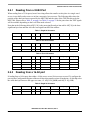
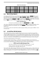
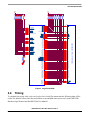
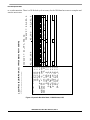
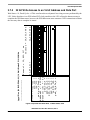
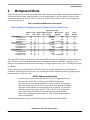
Freescale Semiconductor
Application Note
AN2458
Rev. 3, 04/2005
MPC5200 Local Plus
Bus Interface
by: Davide Santo and Oliver Bibel
1
Introduction
The Local Plus Bus is the external bus system of the
MPC5200 processor, which can be used in conjunction
with Flash ROM, SRAM and memory mapped
peripherals sharing data bus pins with ATA and PCI
devices. This application note gives a brief explanation
how to use this interface with memory mapped
peripherals like Flash or SRAM. This application note
does not cover any workarounds required for potential
bugs of the MPC5200 processor. Please refer to the latest
Errata list of the MPC5200 available from the Freescale
web page.
2
General Features of the
Local Plus Bus
The Local Plus Bus has a total of eight independent chip
selects, 32 Address / Data lines (AD lines) and nine
control lines (LP_R/W_b, LP_ALE_b, LP_TS_b,
LP_ACK, BANK_SEL[1:0] and TSIZ[1:0] and
LP_OE_b). The same physical pins can be used for
© Freescale Semiconductor, Inc., 2005. All rights reserved.
Table of Contents
1
2
3
4
5
Introduction . . . . . . . . . . . . . . . . . . . . . . . . . . . . . . 1
General Features of the Local Plus Bus . . . . . . . . 1
Non-Multiplexed Mode . . . . . . . . . . . . . . . . . . . . . 9
Multiplexed Mode . . . . . . . . . . . . . . . . . . . . . . . . 22
BestComm Interface to the Local Plus Bus . . . . 32
General Features of the Local Plus Bus
different functions depending on the interface type and they might not all available at the same time.
On the same data bus several PCI devices (if more than one external PCI device with bus master
capabilities is intended to be used an external Priority Encoder for the single build in GNT/REQ pair needs
to be added), an ATA device and up to eight generic memory mapped peripherals like Flash, FPGAs,
SRAM, E2PROM, etc. could coexist and each of these devices may need a different kind of transaction.
For example, PCI uses dual tenure (first the address, then the data are driven on the bus) while Flash might
need address and data lines driven at the same time. Another example is ATA which uses a 16-bit wide
bus, while external UART controllers usually come with an 8-bit wide bus.
Other time a specific peripheral implements a subset of a PowerPC 60x-like interface using the LP_TS_b,
LP_R/W_b and LP_ACK signals (for instance the EPSON-SEIKO LCD controller SD13806) or they
might need a separate Read and Write bar with also an Output Enable (e.g. AMD Flash devices as
AM29LV065).
2.1
New Local Plus Bus Features of the MPC5200
Two new operating modes called Large Flash and Most/Graphic have been implemented in the Local Plus
interface.
They both can be used to BOOT MPC5200 using normal off-the shelf ROM memory devices without the
need for external glue logic. The Large Flash interface supports up to 64 Mbytes (it has 26 address lines
A25-A0 and 16 bit data lines D16-D0, where the higher ordered number indicates always the Most
Significant bit), while the Most/Graphic interface covers up to 16 Mbytes (24 Address by 32 Data bus
width). Both have TSIZ signals and LP_OE_b directly available.
The MPC5200 processor has been designed using the ‘same’ package (PBGA 272 pins) as its predecessor.
Therefore the two newly introduced interfaces share now some pins with the PCI/ATA interface preventing
them from being simultaneously used at any moment during MPC5200 operations (not only during
BOOT).
The basic rule is that PCI is mutually exclusive with the Large Flash or Most/Graphic (but not with the
legacy modes of the Local Plus), while ATA can be used with all the legacy modes plus the Large Flash
Interface but not with the MOST graphic one.
At power on the PCI controller is in a reset state to avoid possible contention on the Local Plus Bus thus
preventing a correct boot process from happening. The PCI controller is taken out of reset via a control bit
(bit 16 of the GPIO Port Configuration Register located at MBAR + 0x0B00).
ATA is a chip select controlled interface, then it will not interfere during Boot. It is important to recall that
the MPC5200 ATA controller does NOT provide for a reset line to be connected to the SW_RESET (pin
#1 of the standard 40 pin ATA connector); this line must be implemented via a GPIO.
Two new Power On Reset Configuration Pins (large_flash_sel connected to ball K02 and
most_graphic_sel connected to ball K01) allow the user to select one of the 2 modes for booting.
Only one of the two new modes can be selected at the time; if both POR Configuration pins are set to a
logic ‘1’ the LPC will not boot properly or as expected. If none of them is selected then one of the legacy
booting mode, either not-muxed or muxed, is automatically used.
MPC5200 Local Plus Bus Interface, Rev. 3
2
Freescale Semiconductor
General Features of the Local Plus Bus
As a second new feature for the MPC5200 processor there is the support for today most common burst
flash (see as reference the Intel 28F160F3 or AMD29BL802C or ST Microelectronic M58BW016) to
reduce the total booting time. Full Bursting is supported for Read only (no write) by the Local Plus
controller on the Large Flash, Most/Graphic operating modes.
If the bursting controlled device supports ‘Critical Double Word First (CDWF)’ wrapping order, then a
complete ‘cache line’ (32 Words) can be read in at the time. When this is not the case, the Local Plus
controller can downgrade an internal XLB request to a ‘cache word’ size (64 bits per beat).
All of this happens dynamically in the LPC hardware: if an 8-byte XLB fetch happens (i.e.instruction
fetch), then a 64 bit Burst will occur at the peripheral. If an XLB 32-byte cache line fetch happens, then a
cache Line burst will occur at the peripheral. It is not possible to burst using an access less that the port
size. Bursting mode (64 bit versus CDWF mode) must programmed via SW before first burst transaction
can be performed.
Up to three dead cycles can be inserted in a read (Not in a write access!) to better adapt to different
peripheral’s hold time requirements. Dead cycles are at boot set to the maximum possible (3) and are
programmed via SW. The dead cycles (when set to 0 or 1) can be ‘hidden’ by arbitration cycles and do not
add to them.
The Local Plus in the MPC5200 is also hooked to the internal DMA engine (BestComm) allowing data
movement to be generated independently from CPU. The interface has been implemented by using a single
FIFO (512 bytes deep), which means that the data movement can only happen in a single direction, TX or
RX, at the time (i.e. only Half Duplex communication is possible).
Last the Local Plus being shared among different controllers (PCI, ATA, LPC) is arbitrated by a dedicated
arbiter which adds ‘Bus Parking’ as new feature in the MPC5200. ‘Bus Parking’ is not available for an
external Master (such as an external PCI Initiator device).
The Local Plus Bus interface, being so flexible, can be adjusted to meet all its different operating modes
by means of software configuration and in some cases minimal external logic (in the multiplexed mode
precisely).
NOTE: Multiplexed versus Non-Multiplexed Mode
The most important concept to understand are the Local Plus’ two main
modes of operation: multiplexed mode and non-multiplexed mode
(Bursting can happen ONLY in a non-multiplexed mode of the Local
Plus).
2.2
How to connect a peripheral to the Local Plus Bus
MPC5200 supports the PCI bus naming convention on the Local Plus Bus. This means that the byte
ordering of the external pins conforms to the little endianess rule typical for PCI.
Having a PowerPC core inside, the MPC5200’s internal registers, the internal memory and peripherals’
bus (XLB and IPBI bus) adhere instead to the big endian ordering rule. Please refer to the MPC5200 User
Manual for more details about the XLBus and the IPBI.
The swap is automatically done in the Local Plus module and it is completely transparent to the user.
MPC5200 Local Plus Bus Interface, Rev. 3
Freescale Semiconductor
3
General Features of the Local Plus Bus
2.3
MSBs and LSBs
To connect an external device to the Local Plus Bus a couple of simple rules can be used regardless of the
mode the bus will use to control the device itself:
• A lower bit number in the pin name indicates lower importance of the line in terms of the bit
ordering (‘0’ is always the least significant bit).
• MPC5200’s Local Plus Bus pins are called AD[31:0] where bit 31 is the most significant bit and
bit 0 is the least significant bit.
• PCI-mode: All 32 bits AD[31:0] are used.
• ATA-mode: Data is connected to AD[15:0] and address to AD[18:16].
2.4
Dynamic Bus Access: The Transfer Size Bits
The Local Plus bus allows dynamic bus sizing in the terms that on any chip select a transaction of up to
128-bit data width (a Cache line) is allowed and performed transparently to the user.
Dynamic Bus Access refers to any XLB transaction size that is different (larger or shorter) than the LPC
data port size, thus forcing the LPC to dynamically break the transactions down into multiple LPC bus
tenures in order to assemble/disassemble the XLB data transfer onto the LPC bus.
As an example an “instruction fetch” beat (64 bit long) is supported by the Local Plus controller, which
translates it into the correct number of external access either 2 for the Most/Graphic interface or 4 for the
Large Flash.
The Local Plus controller supports XLB cache-line bursting (32 byte long) assuming that the memory
device also supports the Critical Double Word First ordering scheme. These modes of the Local Plus are
software programmable; please refer to the PowerPC user manual (e.g. refer to “MPC603e & EC603e Risc
Microprocessor User Manual”) and to the MPC5200 User Manual for further details.
During a Local Plus access using either the legacy multiplexed or the Large Flash or the Most/Graphic
mode Transfer Size bits and the address line A0 (LSB) and A1 are put on the bus to reflect the specified
transaction similar to the usual dynamic bus access of PowerPC family microprocessors.
Specifically in the Muxed Mode three Transfer Size bits TSIZ[0:2] are available (on AD[30:28] during the
address tenure), where the most significant one TSIZ[0] is reserved for future use. On the Large Flash and
Most graphic mode only TSIZ[1:2] have been pinned out. The meaning of the TSIZ[1:2] is in any case the
same for the muxed mode and the Large Flash or Most graphic modes.
2.5
Transfer alignment
To illustrate transfer alignments on the bus the following example assumes that the processor performs a
transaction where a 32-bit word, e.g. 0x1234ABCD, is read in one 32-bit, two 16-bit or four 8-bit accesses,
respectively.
MPC5200 Local Plus Bus Interface, Rev. 3
4
Freescale Semiconductor
General Features of the Local Plus Bus
2.5.1
Reading From a 32-Bit Port
When reading from a 32-bit port dynamic bus sizing allows the transfer to take place in a single word
access, in two half word accesses or in four consecutive byte accesses. The following tables show the
position of the data byte lanes expected by the MPC5200 and the value of the TSIZ bits driven by the
MPC5200. Please refer to Table 11 on page 9 or Table 13 on page 22 for the pins where the TSIZ signals
will be available depending on the Local Plus mode selected.
Note that in the following tables AD[31:24] is the most significant byte lane while AD[7:0] is the least
significant byte lane and that A0 is the least significant bit of the address.
Table 1. Single 32-bit access
TSIZ1
TSIZ2
A1
A0
AD[31:24]
AD[23:16]
AD[15:8]
AD[7:0]
0
0
0
0
0x12
0x34
0xAB
0xCD
AD[15:8]
AD[7:0]
0xAB
0XCD
AD[15:8]
AD[7:0]
Table 2. Two 16-bit access
TSIZ1
TSIZ2
A1
A0
AD[31:24]
AD[23:16]
1
0
0
0
0x12
0x34
1
0
1
0
Table 3. Four 8-bit access
2.5.2
TSIZ1
TSIZ2
A1
A0
AD[31:24]
0
1
0
0
0x12
0
1
0
1
0
1
1
0
0
1
1
1
AD[23:16]
0x34
0xAB
0xCD
Reading from a 16-bit port
If reading from a 16-bit port, then either a 16-bit access or two 8-bit accesses are used. To configure the
port size the Configuration Register of the used chip select must be written. Note that in a 16-bit chip select
the valid data byte lanes are the upper two ones, i.e. AD[31:24] (MSB) and AD[23:16] (LSB).
Table 4. Single 16-bit access
TSIZ1
TSIZ2
A1
A0
AD[31:24]
AD[23:16]
1
0
0
0
0x12
0x34
1
0
1
0
0xAB
0XCD
AD[15:8]
AD[7:0]
MPC5200 Local Plus Bus Interface, Rev. 3
Freescale Semiconductor
5
General Features of the Local Plus Bus
Table 5. Two 8-bit access
2.5.3
TSIZ1
TSIZ2
A1
A0
AD[31:24]
0
1
0
0
0x12
0
1
0
1
0
1
1
0
0
1
1
1
AD[23:16]
AD[15:8]
AD[7:0]
0x34
0xAB
0xCD
Reading from a 8-bit port
With data contents as before, now the chip select is configured as a single byte located on AD[31:24]. Therefore, only four
consecutive accesses are used. It must be noted that this is transparent to the user.
Table 6. Four 8-bit access
2.5.4
TSIZ1
TSIZ2
A1
A0
AD[31:24]
0
1
0
0
0x12
0
1
0
1
0x34
0
1
1
0
0xAB
0
1
1
1
0xCD
AD[23:16]
AD[15:8]
AD[7:0]
Write Transaction
This example details a 32-bit write transaction. As before the value 0x1234ABCD is used to demonstrate a 32-bit, two 16-bit or
four 8-bits write accesses of the MPC5200 to a peripheral.
Table 7. Single 32-bit access
TSIZ1
TSIZ2
A1
A0
AD[31:24]
AD[23:16]
AD[15:8]
AD[7:0]
0
0
0
0
0x12
0x34
0xAB
0xCD
AD[15:8]
AD[7:0]
0xAB
0XCD
Table 8. Two 16-bit access
TSIZ1
TSIZ2
A1
A0
AD[31:24]
AD[23:16]
1
0
0
0
0x12
0x34
1
0
1
0
0xAB
0XCD
MPC5200 Local Plus Bus Interface, Rev. 3
6
Freescale Semiconductor
General Features of the Local Plus Bus
Table 9. Four 8-bit access
2.6
TSIZ1
TSIZ2
A1
A0
AD[31:24]
0
1
0
0
0x12
0
1
0
1
0x34
0
1
1
0
0xAB
0
1
1
1
0xCD
AD[23:16]
AD[15:8]
AD[7:0]
0x34
0xAB
0xCD
Boot Chip Select
For booting the MPC5200 uses a special chip select called Chip Select Boot (CSBOOT). This signal is
physically tied to the same ball as chip select 0 (CS0). CSBOOT and CS0 also share the configuration
register located at offset 0x0300 from the module base address (MBAR). The only difference between the
two ‘virtual’ chip selects (CSBOOT and CS0) lies in the fact that CSBOOT is enabled after reset (during
boot) and CS0 must first be enabled by software before it can be used as a CS line.
NOTE: Code Execution
Code can be executed from any chip select (CSBOOT, CS0 through CS7).
Also, the two virtual chip select have different mapping registers. CS0 start and stop virtual address values
are mapped at MBAR+0x04 and MBAR+0x08, while CSBOOT is mapped at MBAR+0x4C and
MBAR+0x50.
It is essential to avoid to have both of them enabled (using the enabling control register at MBAR + 0x54)
at the same time.
2.7
Local Plus Performance
The Local Plus interface has been originally designed to be an easy-to-use interface not specifically
focused on high speed performance. For this reason arbitration of the bus (there can be different masters
on the Local Plus as the processor core, an external PCI master and different targets could be accessed such
as ATA, PCI or an external memory mapped device) may be performed at every new access. This of course
adds some overhead time, which should be taken into consideration when trying to evaluate the speed
characteristics and performances of this interface.
As already mentioned ‘Bus Parking’ is available but only for internal Masters (LP controller, PCI
controller and ATA controller). This feature improves performances allowing a Master to have immediate
access to the bus without having to re-arbitrate as long as no other requests are pending.
NOTE: Local Plus Bus Reference Clock
MPC5200 is using the PCI clock as the internal reference clock. As a result
all clock counts are with respect to the PCI clock. All transitions are
synchronized to the rising edge of the PCI clock.
The Local Plus has a BestComm hook. Therefore Local Plus can directly transfer in a DMA fashion data
from the target to BestComm’s FIFOs, thus increasing performance. The BestComm interface is a Half
Duplex only designed on a 512 deep FIFO. Alarm and granularity level can be set via SW and any CS can
MPC5200 Local Plus Bus Interface, Rev. 3
Freescale Semiconductor
7
Non-Multiplexed Mode
be supported by the internal DMA engine. See <st-blue>Chapter 5, <st-blue><st-italic>BestComm
Interface to the Local Plus Bus, for more details.
XLB bus processing and arbitration cycles are removed from the Local Plus Controller transaction timing
clock counts when the BestComm interface is used.
3
Non-Multiplexed Mode
In non-multiplexed mode, the 32 physical AD pins of the MPC5200 are divided into two separate, non
multiplexed groups, precisely the address and data partitions. This allows data and address to be driven at
the same time on separate pins.
Eight different configurations of address and data lines are supported.
Table 10. Non-Multiplexed Address/Data Size Options
Non Muxed Modes (address and data at the same time)
Mode Name
LegacyNonMuxed 8
LegacyNonMuxed 8
LegacyNonMuxed 8
LegacyNonMuxed 16
LegacyNonMuxed 16
Large Flash 16
Large Flash8
MOST / Graphics 32
Address Data TSIZE
Size
Size
Bits
24
8
16
8
8
8
16
16
8
16
26
16
26
8
24
32
2
Total
BANK Memory Size Memory Size
Bits [Bytes]
[MBytes]
16777216
16
65536
0,0625
256 0,000244141
65536
0,0625
256 0,000244141
67108864
64
64
67108864
16777216
16
Boot
Option
yes
no
no
yes
no
yes
yes
yes
Burst
Support
no
no
no
no
no
yes
yes
yes
ATA
Support
yes
yes
yes
yes
yes
yes
yes
no
PCI
Support
yes
yes
yes
yes
yes
no
no
no
For example a possible booting configuration uses 24 address and 8 data lines and is thus able to address
224 data bytes, or a total of 16 Mbytes. A second configuration uses 16 address and 16 data lines. Here,
215 address lines point at a half-word each for at a total of 64 kBytes.
NOTE: Byte Addressing is used in all modes
16-Bit wide data connection to the peripheral: Any two ‘short’ addresses
[16 bit data] are separated by an 0x02 address offset, which clearly indicates
that A0 lines is never asserted, or used thus it shall not be connected to the
device. The pin A[0] of the controlled device is usually connected to A[1]
of the processor.
32-Bit wide data connection to the peripheral: Any two ‘word’ addresses
[32 bit data] are separated by an 0x04 address offset, which clearly indicates
that A[1:0] lines are never asserted, or used thus they shall not be connected
to the device. The pins A[1:0] of the controlled device are usually connected
to A[3:2] of the processor. The TSIZ[1:2] pins can sometimes be used in
conjunction with A[1:0] to select which byte or short is actually used during
the transfer and allow transfers smaller than the physical connection to the
peripheral. In such case a direct connection from A[1:0] (processor) to
A[1:0] (device) is possible or necessary.
MPC5200 Local Plus Bus Interface, Rev. 3
8
Freescale Semiconductor
Non-Multiplexed Mode
The Non-Multiplexed Mode is able to interface gluelessly with memory mapped external devices like
Flash ROM, E2PROM or SRAM. It is also faster than the multiplexed mode as it provides both data and
address in a single tenure.
The following table shows the Local Plus bus signals of the most important Non-muxed Modes.
Table 11. Local Plus Signals of the most important Non-muxed Modes
Non Muxed Modes (address and data at the same time)
SignalName[MSB:LSB]
Local Plus Bus Signal Functionality Dedending On Mode Configured
Large Flash16 Read
Large Flash16
Burst Enabled
MPC5200 Signal Name LegacyNonMuxed8 LegacyNonMuxed16
Read / Write
Read / Write
Read / Write
Read / Write
LP_R/W_b
LP_ALE_b
Transfer Acknowledge Transfer Acknowledge Transfer Acknowledge
Burst Advance
LP_ACK_b
LP_TS_b
-
-
Transfer Start
LP_OE_b
CS[7:0]
LP_AD[31:24]
LP_AD[23:16]
LP_AD[15:8]
LP_AD[7:0]
TSIZE_1
TEST_SEL_1
PCI_CLK
PCI_PAR
PCI_C/BE_0
PCI_C/BE_1
PCI_C/BE_2
PCI_C/BE_3
PCI_TRDY
PCI_IRDY
PCI_STOP
PCI_DEVSEL
PCI_FRAME
PCI_SERR
PCI_PERR
PCI_IDSEL
PCI_REQ
PCI_GNT
PCI_RESET
ATA_DRQ
ATA_DACK
ATA_IOR
ATA_IOW
ATA_IOCHDRY
ATA_INTRQ
ATA_ISOLATION
Output Enable
CS[7:0]
D[7:0]
A[23:16]
A[15:8]
A[7:0]
PCI_CLK
-
Output Enable
CS[7:0]
D[15:8]
D[7:0]
A[15:8]
A[7:0]
PCI_CLK
-
Output Enable
CS[7:0]
D[15:8]
D[7:0]
A[15:8]
A[7:0]
PCI_CLK
A16
A17
A18
A19
A20
A21
A22
A23
A24
A25
-
3.1
3.1.1
Start Address for
Burst
Output Enable
CS[7:0]
D[15:8]
D[7:0]
A[15:8]
A[7:0]
PCI_CLK
A16
A17
A18
A19
A20
A21
A22
A23
A24
A25
-
MOST / Graphics
MOST / Graphics Read Burst Enabled
32
32
Read / Write
Read / Write
A23
A23
Transfer
Burst Advance
Acknowledge
Transfer Start
Start Address for
Burst
Output Enable
Output Enable
CS[7:0]
CS[7:0]
D[31:24]
D[31:24]
D[23:16]
D[23:16]
D[15:8]
D[15:8]
D[7:0]
D[7:0]
TSIZE1
TSIZE1
TSIZE2
TSIZE2
PCI_CLK
PCI_CLK
A0
A0
A1
A1
A2
A2
A3
A3
A4
A4
A5
A5
A6
A6
A7
A7
A8
A8
A9
A9
A10
A10
A11
A11
A12
A12
A13
A13
A14
A14
A15
A15
A16
A16
A17
A17
A18
A18
A19
A19
A20
A20
A21
A21
A22
A22
Special Dedicated Local Plus Signals
Transfer Acknowledge (LP_ACK_b)
The use of LP_ACK_b for termination is software programmable. The LP_ACK_b, when input, can only
reduce the maximum programmed duration of the chip select transaction but never prolong it. The same
pin can be used as an output in the Most/Graphics and Large Flash interface indicating the burst advance
of a burst access.
MPC5200 Local Plus Bus Interface, Rev. 3
Freescale Semiconductor
9
Non-Multiplexed Mode
NOTE: Acknowledge active during boot
The LP_ACK_b functionality is enabled during boot and therefore requires
a pull up resistor to disable the acknowledge input in case the peripheral
from which the boot code is fetched does not support the acknowledge
feature.
3.1.2
Address Latch Enable (LP_ALE_b)
This signal serves as the additional address line A23 when MOST/Graphics mode is selected.
3.1.3
Transfer Start (LP_TS_b)
This pin can be used as an output in the Most/Graphics mode (burst mode only) and Large Flash mode
(burst mode only) indicating a valid start address for the next burst transfer.
3.2
3.2.1
Configuration options
Wait States
The numbers for read and write wait states can be set independently. The wait states are counted in PCI
clock cycles.
3.2.2
Dead Cycles
Dead cycles after a read access can be inserted (up to three as chosen by the user via software) to provide
for proper peripheral hold time. Some dead cycles might be hidden by arbitration.
In either case the data and control signals will be maintained one clock cycle beyond CSx negation to
assure hold time.
3.3
Booting
At boot by default (via the Hardware Reset Word) the wait states inserted can be either 4 PCI clock cycles
or 48 PCI clock cycles. This value can be changed by software to anything from 0 to 127 (or even more
when a prescaler is used) once the boot process has successfully started.
Normally a slow device such as Flash ROM memory may need some waits states and therefore at the very
boot it might be necessary to start the MPC5200 with the longest wait state default (48 PCI Clocks = 727
ns at the maximum allowed Local Plus speed of 66 MHz).
3.4
How to connect a Flash device in a legacy mode
This example assumes the use of a byte wide Flash device with an address space of 8 MBytes. In this case
the 24-address/8-bit data non-multiplexed mode can be used. The AD pins are split in two groups the
following way: AD[23:0] are used as address lines A[23:0] and AD[31:24] are used as data lines D[7:0].
MPC5200 Local Plus Bus Interface, Rev. 3
10
Freescale Semiconductor
Non-Multiplexed Mode
With this convention the Address and the Data bus can be directly connected to the device. In fact, A0 is
the least significant bit of the address section of the Local Plus interface while D[0] (connected to AD[24]
on the processor) is the least significant bit of the data byte lane.
R10
R11
R12
R13
R14
R15
R16
R17
R18
R19
R20
10K
10K
10K
10K
10K
U2
U1A
Y 19
Y 18
W18
Y 17
W17
V17
Y 16
PCI_GNT
PCI_RESET
PCI_CLOCK
PCI_IDSEL
PCI_REQ
PCI_C/BE_3
PCI_C/BE_2
PCI_C/BE_1
PCI_C/BE_0
PCI_FRAME
PCI_TRDY
PCI_STOP
PCI_IRDY
PCI_PAR
PCI_DEVSEL
PCI_PERR
PCI_SERR
R21
R22
R4
R2
T1
U2
U1
Y2
W6
Y8
W10
V5
W5
V6
Y6
V7
W7
Y7
W8
ATA_INTRQ
ATA_DACK
ATA_IOCHDRY
ATA_IOR
ATA_IOW
ATA_DRQ
ATA_ISOLATION
CS0
CS1
CS2
CS3
CS4
CS5
LP_OE
LP_TS
LP_ACK
LP_ALE
LP_R/W
AD0
AD1
AD2
AD3
AD4
AD5
AD6
AD7
AD8
AD9
AD10
AD11
AD12
AD13
AD14
AD15
10K
5K6
AD16
AD17
AD18
AD19
AD20
AD21
AD22
AD23
AD24
AD25
AD26
AD27
AD28
AD29
AD30
AD31
IRQ_0
IRQ_1
IRQ_2
IRQ_3
W14
Y 14
V15
W15
Y 15
V16
H2
D8
Y 13
U14
V14
W16
J2
C5
V13
W13
V12
Y 12
V11
W12
U11
Y 11
G2
F2
E2
C2
D2
F3
E3
C3
W11
V10
Y 10
V9
Y9
V8
W9
U8
D6
C6
H6
E6
F6
D7
C7
E7
W4
Y5
V4
Y4
V2
Y3
V3
W3
F7
G7
D3
G6
J7
K4
E5
U3
W2
T2
Y1
T3
W1
R3
V1
G3
K3
G4
H4
K5
G5
J6
K6
P3
P1
P2
R1
C4
CE
OE
WE
A0
A1
A2
A3
A4
A5
A6
A7
A8
A9
A10
A11
A12
A13
A14
A15
A16
A17
A18
A19
A20
A21
A22
8MByte Flash, AM29LV065D
R9
1K
10K
10K
10K
10K
10K
10K
R1
R2
R3
R4
R5
R6
R7
R8
3.3V
5K6
5K6
5K6
5K6
5K6
5K6
5K6
5K6
3.3V
DQ0
DQ1
DQ2
DQ3
DQ4
DQ5
DQ6
DQ7
RY /BY
AM29LV065D
MPC5200
Figure 1. Legacy Non-Multiplexed Mode
MPC5200 Local Plus Bus Interface, Rev. 3
Freescale Semiconductor
11
Non-Multiplexed Mode
3.5
How to connect a Flash device in the Large Flash
Mode
This example assumes the use of a synchronous 16 Bit wide Flash device with an address space of 1 MByte
that supports burst reads. Figure 2 shows how the Local Plus pins have to be connected to the flash device.
It should be noted that also some PCI signals are used to extend the address range of the Local Plus Bus
during Local Plus transfers. A maximum of 26 address lines (A[25:0]) is available in the Large Flash
mode. In this example only A[19:1] are required to cover the whole address range of the flash device
connected. A[0] is the LSB of the address section of the Local Plus interface and D[0] is the LSB of the
data byte lane.
MPC5200 Local Plus Bus Interface, Rev. 3
12
Freescale Semiconductor
Non-Multiplexed Mode
R4
R2
U2
U1
Y2
V5
W5
V6
Y6
PCI_GNT
PCI_RESET
PCI_IDSEL
PCI_REQ
PCI_C/BE_3
PCI_FRAME
PCI_TRDY
PCI_STOP
PCI_IRDY
PCI_DEVSEL
PCI_PERR
PCI_SERR
10K
5K6
R22
R23
W7
Y7
W8
ATA_INTRQ
ATA_DACK
ATA_IOCHDRY
ATA_IOR
ATA_IOW
ATA_DRQ
ATA_ISOLATION
LP_OE
LP_TS
LP_ACK
LP_ALE
LP_R/W
AD0
AD1
AD2
AD3
AD4
AD5
AD6
AD7
AD8
AD9
AD10
AD11
AD12
AD13
AD14
AD15
PCI_PAR
PCI_C/BE_0
PCI_C/BE_1
PCI_C/BE_2
AD16
AD17
AD18
AD19
AD20
AD21
AD22
AD23
AD24
AD25
AD26
AD27
AD28
AD29
AD30
AD31
IRQ_0
IRQ_1
IRQ_2
IRQ_3
R16
R17
R18
R19
R20
R21
10K
10K
10K
10K
10K
10K
W14
Y 14
V15
W15
Y 15
V16
T1
D8
Y 13
U14
V14
W16
14
27
17
56
28
1
V13
W13
V12
Y 12
V11
W12
U11
Y 11
W11
13
12
11
10
9
8
7
6
V10
Y 10
V9
Y9
V8
W9
U8
V7
W10
Y8
W6
52
51
50
49
48
47
46
45
44
5
4
W4
Y5
V4
Y4
V2
Y3
V3
W3
18
20
22
24
33
35
37
39
U3
W2
T2
Y1
T3
W1
R3
V1
19
21
23
25
34
36
38
40
P3
P1
P2
R1
3
30
U2
CE#
CLK
OE#
LBA#
BAA#
WE#
A0
A1
A2
A3
A4
A5
A6
A7
A8
A9
A10
A11
A12
A13
A14
A15
A16
A17
A18
DQ0
DQ1
DQ2
DQ3
DQ4
DQ5
DQ6
DQ7
1MByte Burst Flash, AM29BL802C
Y 19
Y 18
W18
Y 17
W17
V17
Y 16
CS0
CS1
CS2
CS3
CS4
CS5
PCI_CLOCK
R10
R11
R12
R13
R14
R15
R9
1K
U1A
10K
10K
10K
10K
10K
10K
R1
R2
R3
R4
R5
R6
R7
R8
3.3V
5K6
5K6
5K6
5K6
5K6
5K6
5K6
5K6
3.3V
DQ8
DQ9
DQ10
DQ11
DQ12
DQ13
DQ14
DQ15
RY /BY#
IND#
AM29BL802C
MPC5200
Figure 2. Large Flash Mode
3.6
Timing
To calculate how many clock cycles are involved in a Local Plus transaction the following data will be
useful. For detailed values, like data and address set up and hold times, please refer to the MPC5200
Hardware Specification and the MPC5200 User Manual.
MPC5200 Local Plus Bus Interface, Rev. 3
Freescale Semiconductor
13
Non-Multiplexed Mode
The number of clock cycles given below will be per data beat, which is based on the port size (it could be
8-bit or 16-bit or 32-bit). The reference clock is the PCI clock.
These numbers provide the best case timing, where it is assumed that the PCI arbiter is parked on the Local
Plus controller, there is no other traffic on the internal Bus (XLB), and pipelining of the XLB is enabled.
The XLB, for future reference, is the processor core’s bus (PPC 60X Local Bus). Again the Wait states
must be computed in terms of PCI clock cycles. XLB pipeline can be turned on/off via SW control (the
control register belongs to the XLB Arbiter register group). Pipelining refers to the possibility to start
internally on the XLB bus a second address tenure while the data tenure corresponding to the previous
address has not yet terminated (either with a TA or a TEA). It might increases performances depending on
the application.
With Dynamic Bus Sizing is important to remember that when a wider piece of data is decomposed in
smaller chunks to adapt to the peripheral size no additional overhead is added. Nonetheless any time a new
data (32 or 64 bit long) is to be read/written from the core a ‘turnaround’ overhead clock is needed. This
is calculated by the formula:
Overhead Clock = 4 x PCI/XLB clock ratio.
Eqn. 1
Last is to note that while a normal PowerPC data or instruction can be maximum be 32-bit wide, an
instruction fetch has always a size of 64 bit (to make full usage of the internal instruction pipeline).Write
Access:
3.6.1
•
•
•
•
•
•
Write Access
1 Setup
1 CS assertion
W = number of waits states (0 to 127)
4 * pci/xlb clock ratio 1
1 LPC processing 2
4 * pci/xlb clock ratio 3
For an internal clock ratio of the XLB:IPBI:PCI = 4:2:1, a minimum of 4 pci clocks+W per bus tenure is
needed for back-to-back writes.
3.6.2
•
•
•
•
•
Read Access (non burst)
1 Setup
1 CS assertion
W = number of waits states (0 to 127)
D = programmable dead cycles (0 to 3) to allow peripheral time to 3-state bus after read
1 LPC processing (this may be masked by dead cycles if set to 1 or greater)
1. Do not add this cycle if the transaction is a dynamic LPC bus tenure.
2. Assumes the PCI arbiter is parked on the LPC, else this number is dependent upon Local Plus Bus traffic.
3. Add these cycle(s) to the count if XLB pipelining is turned off.
MPC5200 Local Plus Bus Interface, Rev. 3
14
Freescale Semiconductor
Non-Multiplexed Mode
•
•
•
4 * pci/xlb clock ratio 1
1 LPC processing 2
4 * pci/xlb clock ratio 3
For an internal clock ratio of the XLB:IPBI:PCI = 4:2:1, a minimum of 5 PCI clocks+W+D per bus tenure
is needed for back-to-back reads.
3.7
Waveform Snapshots
The following pages contain snapshots of simulation waveforms for the following Local Plus port
configurations:
• Non-muxed 32-bit XLB read transaction to 16-bit address and 16-bit data port, resulting in
dynamic Local Plus Controller accesses. Wait States=14, Dead Cycles=0.
• Non-muxed 32-bit XLB write transaction to 16-bit address and 16-bit data port, resulting in
dynamic Local Plus Controller accesses. Wait States=4, Dead Cycles=0.
• Non-muxed 16-bit read transaction to 26-bit address and 16-bit data port, Wait States=5, Dead
Cycles=0
• Non-muxed 16-bit write transaction to 26-bit address and 16-bit data port, Wait States=5, Dead
Cycles=0
• Non-muxed 16-bit short burst read transaction to 26-bit address and 16-bit data port, Wait
States=5, Dead Cycles=0
The simulations were run under the following conditions allowing for maximum performance on the Local
Plus Bus:
• Clock ratio as indicated in the figures. E.g. clock ratio = 4:2:1 (133MHz, 66MHz, 33MHz)
• No other XLB traffic is present so XLB arbitration is dedicated to Zeppo core read/write access
to/from the Local Plus Controller.
• No other Local Plus Bus traffic is present so the PCI arbiter remains parked on the Local Plus
Controller.
These simulated conditions are characteristic of the conditions that would exist during boot operations,
where pipelined read-read and read-write XLB transactions are not pipelined.
3.7.1
32 bit Read Access to an 16 bit Address and Data Port
Wait State = 14, Dead Cycle = 0
Eqn. 2
This transaction shows a back-to-back LPC read access. The visible LPC transactions correspond to the
first two XLB bus tenures. The second XLB address/data bus tenure is pipelined with respect to the first
address/data bus tenure. As a result, XLB arbitration cycles do not impact the LPC as it goes from a write
1. Do not add this cycle if the transaction is a dynamic LPC bus tenure.
2. Assumes the PCI arbiter is parked on the LPC, else this number is dependent upon Local Plus Bus traffic.
3. Add these cycle(s) to the count if XLB pipelining is turned off.
MPC5200 Local Plus Bus Interface, Rev. 3
Freescale Semiconductor
15
16
*
*
42,681.6
3FF0026
FFFF
2728
42,000
Cursor1 = 41,393.664 ns
Cursor2 = 42,681.6
41,393.664
Group: LocalPLUS
xlb_clk = 1
ipg_clk = 1
pad_pci_clock = 1
Address% = ’h 3FF002 3* 3FF0024
Data%[31:16] = ’h 23 2* FFFF
2526
pad_csb_4 = 0
pad_lp_ts_b = 1
pad_lp_ack_b = 1
pad_lp_oe_b = 0
pad_lp_rwb = 1
pad_lp_ale_b = 1
MPC5200: 16+16 Not Muxed Mode: Dynamic Access (32 bit READ)
D.SANTO
Local Plus (XLB:IP:PCI=4:2:1) 14 Wait States PCI @ 33 MHz
Non-Multiplexed Mode
to a read transaction. There is a XLB clock cycle necessary for the XLB data bus tenure to complete and
start the next tenure.
Figure 3. Dynamic Bus Size Read, 14 Wait States, 0 DC
MPC5200 Local Plus Bus Interface, Rev. 3
Freescale Semiconductor
Non-Multiplexed Mode
3.7.2
32 bit Write Access to an 16 bit Address and Data Port
**
**
3FF0026
2728
34,053.068 ns
32,893.017
Group: LocalPLUS
xlb_clk = 0
ipg_clk = 1
pad_pci_clock = 1
Address% = ’h 3FF002 * 3FF0024
Data%[31:16] = ’h 23 * 2526
pad_csb_4 = 1
pad_lp_ts_b = 1
pad_lp_ack_b = 1
pad_lp_oe_b = 1
pad_lp_rwb = 0
pad_lp_ale_b = 1
Cursor1 = 32,893.017 ns
Cursor2 = 34,053.068 ns
MPC5200: 16+16 Not Muxed Mode: Dynamic Access (32 bit WRITE)
D.SANTO
Local Plus (XLB:IP:PCI=4:2:1) 14 Wait States PCI @ 33 MHz
Wait States = 14, Dead Cycles = 0.This waveform shows a dynamic bus sizing accesses performed by the
LPC. Notice that there is no XLB related PCI clock penalties as the LPC collects the data necessary to
complete the XLB data tenure; however, the XLB data tenure now consumes 2 LPC transactions to obtain
the necessary data to complete its tenure.
Figure 4. Dynamic Bus Size Write, 14 Wait States, 0 DC
MPC5200 Local Plus Bus Interface, Rev. 3
Freescale Semiconductor
17
18
3FF0* 3*
5* FFFF 0*
1,792,265.333 ns
Cursor1 = 1,792,162.944 ns
Cursor2 = 1,792,192.896 ns
1,791,908.12
Group: LocalPLUS
ipg_clk = 1
pad_pci_clock = 0
Address% = ’h 0100166 3FF* 0100166
Data%[31:16] = ’h 5959 0000 FFFF
pad_csb_4 = 0
pad_lp_ts_b = 1
pad_lp_ack_b = 1
pad_lp_oe_b = 0
pad_lp_rwb = 1
pad_lp_ale_b = 1
MPC5200: Large Flash I/F: Single Read
3.7.3
D.SANTO
Local Plus (XLB:IP:PCI=4:4:1) 5 Wait States PCI @ 33 MHz
Non-Multiplexed Mode
Large Flash Read Access
Figure 5. Large Flash Read Access
MPC5200 Local Plus Bus Interface, Rev. 3
Freescale Semiconductor
Freescale Semiconductor
1,498,886.727
3F* 010*
00* 0E0E
1,499,247.533 ns
Cursor1 = 1,499,187.456 ns
Cursor2 = 1,499,217.408 ns
Group: LocalPLUS
ipg_clk = 1
pad_pci_clock = 1
Address% = ’h 3FF0000 3F* 0100036
Data%[31:16] = ’h 0000 00* 0DAA
pad_csb_4 = 1
pad_lp_ts_b = 1
pad_lp_ack_b = 1
pad_lp_oe_b = 1
pad_lp_rwb = 0
pad_lp_ale_b = 1
MPC5200: Large Flash I/F: Write
3.7.4
D.SANTO
Local Plus (XLB:IP:PCI=4:4:1) 5 Wait States PCI @ 33 MHz
Non-Multiplexed Mode
Large Flash Write Access
Figure 6. Large Flash Write Access
MPC5200 Local Plus Bus Interface, Rev. 3
19
20
3FF* 3F* 01*
* * * * FFFF 00* FF*
1,587,367.328 ns
ursor1 = 1,587,201.408 ns
Cursor2 = 1,587,231.36 ns
1,586,871.936
Group: LocalPLUS
ipg_clk = 1
pad_pci_clock = 0
Address% = ’h 01000A8 * 01000A8
Data%[31:16] = ’h 2BAA * FFFF
pad_csb_4 = 0
pad_lp_ts_b = 1
pad_lp_ack_b = 0
pad_lp_oe_b = 0
pad_lp_rwb = 1
pad_lp_ale_b = 1
MPC5200: Large Flash I/F: Burst Read
3.7.5
D.SANTO
Local Plus (XLB:IP:PCI=4:4:1) 5 Wait States PCI @ 33 MHz
Non-Multiplexed Mode
Large Flash Short Burst Read Access
Figure 7. Large Flash Short Burst Read
MPC5200 Local Plus Bus Interface, Rev. 3
Freescale Semiconductor
Multiplexed Mode
4
Multiplexed Mode
Opposed to the previous mode, the multiplexed mode implements the address and data lines multiplexed
on the same physical pins using dual tenure (or time multiplexing). First, the address is driven on the
shared address/data bus and LP_ALE_b is asserted. Then the data is either written or read during the
assertion of chip select.
Table 12. Multiplexed Address/Data Size Options
Muxed Modes (first address tenure followed by the data tenure)
LegacyMuxed 8
LegacyMuxed 8
LegacyMuxed 8
LegacyMuxed 8
LegacyMuxed 16
LegacyMuxed 16
LegacyMuxed 16
LegacyMuxed 16
LegacyMuxed 32
LegacyMuxed 32
LegacyMuxed 32
LegacyMuxed 32
Address Data TSIZE
Size
Size
Bits
25
8
3
24
8
3
16
8
3
8
8
3
25
16
3
24
16
3
16
16
3
8
16
3
25
32
3
24
32
3
16
32
3
8
32
3
Memory Size Total
Memory Size
BANK per Bank
[MBytes]
Bits [Bytes]
2
33554432
128
2
16777216
64
2
65536
0,25
2
256 0,000976563
2
33554432
128
2
16777216
64
2
65536
0,25
2
256 0,000976563
2
33554432
128
2
16777216
64
2
65536
0,25
2
256 0,000976563
Boot
Option
no
no
no
no
yes
no
no
no
yes
no
no
no
Burst
Support
no
no
no
no
no
no
no
no
no
no
no
no
This approach is slower in comparison to the not-multiplexed mode as it multiplexes the bus functions in
time. At least two PCI clocks more than in the non-multiplexed case are needed for each bus access.
However, the multiplexed mode has the advantage of a bigger address space (up to 128 MBytes divided
in 4 Banks).
It also always needs external logic to latch the address in case this function is not provided by the
peripheral. The latch gate must be active low, meaning the latch is transparent when its gating signal is
kept asserted to a logic low value.
NOTE: Address Latch Enable
Attention must be paid to the fact that the LP_ALE_b signals deasserts at
the same time as the CSx_b will assert (see MPC5200 Hardware
Specification for more details about the Local Plus timing). A board trace
delay then might cause the LP_ALE_b to deassert ‘later’ than the CS falling
edge, thus causing Data to be latched instead of an Address. To avoid this
problem a register (driven by the PCI_CLK, with LP_ALE_b gating the
clock itself) can be used. Please refer to the latest Errata sheet of the
MPC5200 regarding limitations of the LP_ALE_b signal implementation
and its workarounds.
The following table shows the Local Plus bus signals available in the Muxed Mode.
MPC5200 Local Plus Bus Interface, Rev. 3
Freescale Semiconductor
21
Multiplexed Mode
Table 13. LocalPlus Signals in Muxed Mode
Muxed Modes (first address tenure followed by the data tenure)
SignalName[MSB:LSB]
Local Plus Bus Signal Functionality Dedending On Mode Configured
MPC5200 Signal Name
LP_R/W_b
LP_ALE_b
LegacyMuxed 8
LegacyMuxed 16
LegacyMuxed 32
Address Phase
Data Phase
Address Phase
Data Phase
Address Phase
Data Phase
Read / Write
Read / Write
Read / Write
Read / Write
Read / Write
Read / Write
Address Latch Enable Address Latch Enable Address Latch Enable Address Latch Enable Address Latch Enable Address Latch Enable
LP_ACK
Transfer Acknowledge Transfer Acknowledge Transfer Acknowledge Transfer Acknowledge Transfer Acknowledge Transfer Acknowledge
LP_TS_b
LP_OE_b
CS[7:0]
LP_AD[31]
LP_AD[30]
LP_AD[29]
LP_AD[28]
LP_AD[27]
LP_AD[26]
LP_AD[25]
LP_AD[24]
LP_AD[23]
LP_AD[22]
LP_AD[21]
LP_AD[20]
LP_AD[19]
LP_AD[18]
LP_AD[17]
LP_AD[16]
LP_AD[15]
LP_AD[14]
LP_AD[13]
LP_AD[12]
LP_AD[11]
LP_AD[10]
LP_AD[9]
LP_AD[8]
LP_AD[7]
LP_AD[6]
LP_AD[5]
LP_AD[4]
LP_AD[3]
LP_AD[2]
LP_AD[1]
LP_AD[0]
PCI_CLK
4.1
Transfer Start
Output Enable
CS[7:0]
0
TSIZE0
TSIZE1
TSIZE2
0
Bank Select Bit 1
Bank Select Bit 0
A24
A23
A22
A21
A20
A19
A18
A17
A16
A15
A14
A13
A12
A11
A10
A9
A8
A7
A6
A5
A4
A3
A2
A1
A0
PCI_CLK
Transfer Start
Output Enable
CS[7:0]
D7
D6
D5
D4
D3
D2
D1
D0
0
0
0
0
0
0
0
0
0
0
0
0
0
0
0
0
0
0
0
0
0
0
0
0
PCI_CLK
Transfer Start
Output Enable
CS[7:0]
0
TSIZE0
TSIZE1
TSIZE2
0
Bank Select Bit 1
Bank Select Bit 0
A24
A23
A22
A21
A20
A19
A18
A17
A16
A15
A14
A13
A12
A11
A10
A9
A8
A7
A6
A5
A4
A3
A2
A1
A0
PCI_CLK
Transfer Start
Output Enable
CS[7:0]
D15
D14
D13
D12
D11
D10
D9
D8
D7
D6
D5
D4
D3
D2
D1
D0
0
0
0
0
0
0
0
0
0
0
0
0
0
0
0
0
PCI_CLK
Transfer Start
Output Enable
CS[7:0]
0
TSIZE0
TSIZE1
TSIZE2
0
Bank Select Bit 1
Bank Select Bit 0
A24
A23
A22
A21
A20
A19
A18
A17
A16
A15
A14
A13
A12
A11
A10
A9
A8
A7
A6
A5
A4
A3
A2
A1
A0
PCI_CLK
Transfer Start
Output Enable
CS[7:0]
D31
D30
D29
D28
D27
D26
D25
D24
D23
D22
D21
D20
D19
D18
D17
D16
D15
D14
D13
D12
D11
D10
D9
D8
D7
D6
D5
D4
D3
D2
D1
D0
PCI_CLK
Special Dedicated Local Plus signals
NOTE: Bursting
Bursting is not available in any of the Muxed Modes.
4.1.1
Transfer Acknowledge (LP_ACK_b)
The use of LP_ACK_b for termination is software programmable. The LP_ACK_b, when input, can only
reduce the maximum programmed duration of the chip select transaction but never prolong it. The same
pin can be used as an output in the Most/Graphics and Large Flash interface indicating the burst advance
of a burst access.
MPC5200 Local Plus Bus Interface, Rev. 3
22
Freescale Semiconductor
Multiplexed Mode
NOTE: Acknowledge active during boot
The LP_ACK_b functionality is enabled during boot and therefore requires
a pull up resistor to disable the acknowledge input in case the peripheral
from which the boot code is fetched does not support the acknowledge
feature.
4.1.2
Address Latch Enable (LP_ALE_b)
This signal serves as the a control signal for an external address latch in all muxed modes. Please note that
there is no hold time left between the release of the LP_ALE_b signal an the assertion of the CS signal.
This might impact some peripherals and must be carefully taken into consideration when designing an
external address register.
4.1.3
Transfer Start (LP_TS_b)
This signal is driven low during the first LP clock (the Local Plus bus is based on the PCI clock), when CS
has been asserted to indicate the data phase of the transfer.
4.1.4
Transfer Size (TSIZ[0:2])
The multiplexed mode also provides the three Transfer Size bits (TSIZ[0:2]). They are available on
AD[30:28] during the address phase of a transfer and are used to signal the size of the current transfer.
NOTE: TSIZ Naming Convention
AD[30] represents TSIZ[0] and it is reserved for future use. This bit is
driven to ‘0’ when a 8 bit or 16 bit transaction is performed and to ‘1’ if a
32-bit transaction is executed. AD[29] represents TSIZ[1] and AD[28]
represents TSIZ[2] during the address phase.
In the Multiplexed Mode the data bus width can be either 8, 16 or 32. The boot modes are limited to 16 or
32 bit data width.
4.2
Booting
At boot 8-bit wide multiplexed mode configuration is not supported. Only 16-bit or 32-bit wide data bus
configurations are supported.
Normally a slow device such as Flash ROM memory may need some waits states and therefore at the very
boot it might be necessary to start the MPC5200 with the longest wait state default (48 PCI = 727 ns at
maximum allowed PCI speed of 66 MHz).
4.3
Connecting an LCD Controller
This example shows how a typical LCD controller, the SD 13806 by Epson-Seiko, can be connected to the
Local Plus Bus in the Muxed Mode. This peripheral has 21 address lines and 16 separate data lines. It also
implements an E-Bus-like interface which makes use of the Transfer Size bits as the control registers are
MPC5200 Local Plus Bus Interface, Rev. 3
Freescale Semiconductor
23
Multiplexed Mode
8-bit wide while graphic data is 16-bits, the Transfer Start (LP_TS_b), Acknowledge (LP_ACK_b) and
LP_R/W_b signals.
R10
R11
R12
R13
R14
R15
R16
10K
U2
U1A
U2
U1
Y2
W6
Y8
W10
V5
W5
V6
Y6
V7
W7
Y7
W8
PCI_GNT
PCI_RESET
PCI_IDSEL
PCI_REQ
PCI_C/BE_3
PCI_C/BE_2
PCI_C/BE_1
PCI_C/BE_0
PCI_FRAME
PCI_TRDY
PCI_STOP
PCI_IRDY
PCI_PAR
PCI_DEVSEL
PCI_PERR
PCI_SERR
LP_OE
LP_TS
LP_ACK
LP_ALE
LP_R/W
PCI_CLOCK
AD0
AD1
AD2
AD3
AD4
AD5
AD6
AD7
R17
R18
BSB
RD/WR
M/REG
D8
Y13
U14
V14
W16
T1
V13
W13
V12
Y12
V11
W12
U11
Y11
RD
WE0
U3
U4
E
CP
D0
D1
D2
D3
D4
D5
D6
D7
Q0
Q1
Q2
Q3
Q4
Q5
Q6
Q7
A0
A1
A2
A3
A4
A5
A6
A7
Q0
Q1
Q2
Q3
Q4
Q5
Q6
Q7
A8
A9
A10
A11
A12
A13
A14
A15
Q0
Q1
Q2
Q3
Q4
Q5
Q6
Q7
A16
A17
A18
A19
A20
U5
E
CP
AD8
AD9
AD10
AD11
AD12
AD13
AD14
AD15
10K
5K6
CS
BUSCLK
74LVC377
R4
R2
ATA_INTRQ
ATA_DACK
ATA_IOCHDRY
ATA_IOR
ATA_IOW
ATA_DRQ
ATA_ISOLATION
W14
Y14
V15
W15
Y15
V16
W11
V10
Y10
V9
Y9
V8
W9
U8
D0
D1
D2
D3
D4
D5
D6
D7
74LVC377
Y19
Y18
W18
Y17
W17
V17
Y16
CS0
CS1
CS2
CS3
CS4
CS5
LCD CONTROLLER, S1D13806
R9
1K
10K
10K
10K
10K
10K
10K
R1
R2
R3
R4
R5
R6
R7
R8
3.3V
5K6
5K6
5K6
5K6
5K6
5K6
5K6
5K6
3.3V
U6
AD24
AD25
AD26
AD27
AD28
AD29
AD30
AD31
W4
Y5
V4
Y4
V2
Y3
V3
W3
D0
D1
D2
D3
D4
D5
D6
D7
74LVC377
E
CP
AD16
AD17
AD18
AD19
AD20
AD21
AD22
AD23
U3
W2
T2
Y1
T3
W1
R3
V1
MPC5200
D0
D1
D2
D3
D4
D5
D6
D7
D8
D9
D10
D11
D12
D13
D14
D15
S1D13806
Figure 8. LCD Controller in 16-Bit Local Plus Multiplexed Mode
It is self evident that a legacy non-multiplexed mode is not viable as there would be either not enough
address line (16 data lines +16 address lines) or not enough data lines (24 data lines + 8 address lines). In
this case either an external logic is required to latch the address during the address tenure or the Large Flash
interface could be used (which then would not allow the usage of PCI on the same design).
The external registers will also store the TSIZ bits (on AD[28] the least significant TSIZ bit and on AD[29]
the most significant TSIZ bit) for the legacy mode. For the Large Flash and Most Graphics interfaces, these
bits are directly available from two separated pins.
MPC5200 Local Plus Bus Interface, Rev. 3
24
Freescale Semiconductor
Multiplexed Mode
To connect the device properly the latched address lines A[20:0] must directly be connected to the A[20:0]
pins of the slave device, while for the data part the lines AD[31:16] will be connected to the pins named
D[15:0] on the LCD controller (AD[16] again being the least significant bit).
4.4
Timing
Please refer to the Hardware Specification of the MPC5200 for detailed timing values of the Local Plus
interface. This chapter shows how to calculate the number of clock cycles one access in the muxed mode
would take.
Note that during data tenure, the decision between data being driven or the AD bit being tri-stated is
dependent on whether the transaction is a Read or a Write and what the programmed data size is. Unused
bits in the data tenure (i.e. those in excess of the programmed data size) will be driven to zero by the Local
Plus Bus controller as a precaution to avoid floating bus condition.
The maximum address space per each single chip select in multiplexed mode is 128 MBytes divided into
four banks of 32 MBytes each. In fact, there are 25 address line (AD[24:0]) and two bank select lines
(AD[26:25]) addressing words (32-bits).
4.4.1
•
•
•
•
•
•
•
Write Access
1 Setup
1 Address Tenure
2 Data Tenures (CS asserted)
W = number of waits states (0 to 127)
4 * pci/xlb clock ratio 1
1 LPC processing 2
4 * pci/xlb clock ratio 3
For an internal clock ratio of the XLB:IPBI:PCI = 4:2:1, a minimum of 6 pci clocks+W per bus tenure is
needed for back-to-back writes.
4.4.2
Read Access
•
•
•
1 Setup
1 Address Tenure
2 data tenures (CS asserted)
•
•
•
W = number of waits states (0 to 127)
D = programmable dead cycles (0 to 3) to allow peripheral time to 3-state bus after read
1 LPC Processing (this may be masked by dead cycles if set to 1 or greater)
1. Do not add this cycle if the transaction is a dynamic LPC bus tenure.
2. Assumes the PCI Arbiter is parked on the LPC, else this number is dependent upon Local Plus Bus traffic.
3. Add these cycle(s) to the count if XLB pipelining is turned off.
MPC5200 Local Plus Bus Interface, Rev. 3
Freescale Semiconductor
25
Multiplexed Mode
•
•
•
4 * pci/xlb clock ratio 1
1 LPC processing 2
4 * pci/xlb clock ratio 3
For an internal clock ratio of the XLB:IPBI:PCI = 4:2:1, a minimum of 7 pci clocks+W+D per bus tenure
is needed for back-to-back reads.
The main difference between the non-muxed and the muxed-mode lies in the fact that an address tenure is
needed.
The data tenure minimum time is 2 PCI clocks.
4.5
External Glue Logic
In case of the muxed mode of the Local Plus Bus it is necessary to add external logic to generate control
signals needed by a peripheral but not supplied by the Local Plus Bus. As mentioned above an external
logic is needed to ‘latch’ or ‘register’ the address during the address tenure.
NOTE: LP_OE_b and Write Enable
Not always a pair of signals like LP_OE_b and a Write Enable is needed.
Some device simply support a direct connection with the LP_R/W_b.
Some peripherals might also take a particularly long time before releasing the bus after a read access is
completed. The Local Plus Bus has a maximum of three dead cycles at the end of a transaction (which can
be reduced for a READ only access to 0 via SW programming) where the bus remains tri-stated allowing
such peripherals to detach from the bus without the risk of a bus contention.
1. Do not add this cycle if the transaction is a dynamic LPC bus tenure.
2. Assumes the PCI Arbiter is parked on the LPC, else this number is dependent upon Local Plus Bus traffic.
3. Add these cycle(s) to the count if XLB pipelining is turned off.
MPC5200 Local Plus Bus Interface, Rev. 3
26
Freescale Semiconductor
Multiplexed Mode
3.3V
3.3V
AD[31:0]
PCI_CLOCK
AD0
AD1
AD2
AD3
AD4
AD5
AD6
AD7
AD8
AD9
AD10
AD11
AD12
AD13
AD14
AD15
10K
5K6
AD16
AD17
AD18
AD19
AD20
AD21
AD22
AD23
AD24
AD25
AD26
AD27
AD28
AD29
AD30
AD31
IRQ_0
MPC5200
LP_OE_b
LP_ALE_b
LP_R/W_b
U4
T1
V13
W13
V12
Y 12
V11
W12
U11
Y 11
AD0
AD1
AD2
AD3
AD4
AD5
AD6
AD7
W11
V10
Y 10
V9
Y9
V8
W9
U8
AD8
AD9
AD10
AD11
AD12
AD13
AD14
AD15
W4
Y5
V4
Y4
V2
Y3
V3
W3
AD16
AD17
AD18
AD19
AD20
AD21
AD22
AD23
U3
W2
T2
Y1
T3
W1
R3
V1
AD24
AD25
AD26
AD27
AD28
AD29
AD30
AD31
P3
IRQ0
U5
E
CP
AD2
AD3
AD4
AD5
AD6
AD7
AD8
AD9
D0
D1
D2
D3
D4
D5
D6
D7
Q0
Q1
Q2
Q3
Q4
Q5
Q6
Q7
A2
A3
A4
A5
A6
A7
A8
A9
U8
E
CP
AD10
AD11
AD12
AD13
AD14
AD15
AD16
AD17
D0
D1
D2
D3
D4
D5
D6
D7
Q0
Q1
Q2
Q3
Q4
Q5
Q6
Q7
A10
A11
A12
A13
A14
A15
A16
A17
U9
E
CP
AD18
AD19
AD20
AD21
AD22
AD23
AD24
AD25
D0
D1
D2
D3
D4
D5
D6
D7
Q0
Q1
Q2
Q3
Q4
Q5
Q6
Q7
A18
A19
A20
A21
A22
A23
A24
G2
F2
E2
C2
D2
F3
E3
C3
A10
A11
A12
A13
A14
A15
A16
A17
D6
C6
H6
E6
F6
D7
C7
E7
A18
A19
A20
A21
A22
A23
A24
F7
G7
D3
G6
J7
K4
E5
A0
A1
A2
A3
A4
A5
A6
A7
A8
A9
A10
A11
A12
A13
A14
A15
DQ0
DQ1
DQ2
DQ3
DQ4
DQ5
DQ6
DQ7
G3
K3
G4
H4
K5
G5
J6
K6
AD0
AD1
AD2
AD3
AD4
AD5
AD6
AD7
A16
A17
A18
A19
A20
A21
A22
H2
J2
C5
C4
A2
A3
A4
A5
A6
A7
A8
A9
G2
F2
E2
C2
D2
F3
E3
C3
A10
A11
A12
A13
A14
A15
A16
A17
D6
C6
H6
E6
F6
D7
C7
E7
A18
A19
A20
A21
A22
A23
A24
F7
G7
D3
G6
J7
K4
E5
AM29LV065D
H2
J2
C5
C4
A2
A3
A4
A5
A6
A7
A8
A9
G2
F2
E2
C2
D2
F3
E3
C3
A10
A11
A12
A13
A14
A15
A16
A17
D6
C6
H6
E6
F6
D7
C7
E7
A18
A19
A20
A21
A22
A23
A24
F7
G7
D3
G6
J7
K4
E5
CE
OE
WE
RY /BY
A0
A1
A2
A3
A4
A5
A6
A7
A8
A9
A10
A11
A12
A13
A14
A15
A0
A1
A2
A3
A4
A5
A6
A7
A8
A9
A10
A11
A12
A13
A14
A15
DQ0
DQ1
DQ2
DQ3
DQ4
DQ5
DQ6
DQ7
G3
K3
G4
H4
K5
G5
J6
K6
AD16
AD17
AD18
AD19
AD20
AD21
AD22
AD23
G3
K3
G4
H4
K5
G5
J6
K6
AD24
AD25
AD26
AD27
AD28
AD29
AD30
AD31
A16
A17
A18
A19
A20
A21
A22
AM29LV065D
U6
CS0_b
LP_OE_b
LP_R/W_b
IRQ0
CE
OE
WE
RY /BY
8MByte Flash,
AM29LV065D
D8
Y 13
U14
V14
W16
A2
A3
A4
A5
A6
A7
A8
A9
U2
CS0_b
LP_OE_b
LP_R/W_b
IRQ0
DQ0
DQ1
DQ2
DQ3
DQ4
DQ5
DQ6
DQ7
G3
K3
G4
H4
K5
G5
J6
K6
A16
A17
A18
A19
A20
A21
A22
AM29LV065D
AD8
AD9
AD10
AD11
AD12
AD13
AD14
AD15
U7
CS0_b
LP_OE_b
LP_R/W_b
IRQ0
H2
J2
C5
C4
A2
A3
A4
A5
A6
A7
A8
A9
G2
F2
E2
C2
D2
F3
E3
C3
A10
A11
A12
A13
A14
A15
A16
A17
D6
C6
H6
E6
F6
D7
C7
E7
A18
A19
A20
A21
A22
A23
A24
F7
G7
D3
G6
J7
K4
E5
CE
OE
WE
RY /BY
A0
A1
A2
A3
A4
A5
A6
A7
A8
A9
A10
A11
A12
A13
A14
A15
8MByte Flash,
AM29LV065D
PCI_IDSEL
PCI_REQ
PCI_C/BE_3
PCI_C/BE_2
PCI_C/BE_1
PCI_C/BE_0
PCI_FRAME
PCI_TRDY
PCI_STOP
PCI_IRDY
PCI_PAR
PCI_DEVSEL
PCI_PERR
PCI_SERR
LP_OE
LP_TS
LP_ACK
LP_ALE
LP_R/W
74LVC377
PCI_GNT
PCI_RESET
R18
R19
U2
U1
Y2
W6
Y8
W10
V5
W5
V6
Y6
V7
W7
Y7
W8
CS0
CS1
CS2
CS3
CS4
CS5
74LVC377
R4
R2
ATA_INTRQ
ATA_DACK
ATA_IOCHDRY
ATA_IOR
ATA_IOW
ATA_DRQ
ATA_ISOLATION
CS0_b
74LVC377
Y 19
Y 18
W18
Y 17
W17
V17
Y 16
W14
Y 14
V15
W15
Y 15
V16
CE
OE
WE
RY /BY
8MByte Flash,
AM29LV065D
U3A
H2
J2
C5
C4
8MByte Flash,
AM29LV065D
10K
10K
10K
10K
10K
10K
10K
10K
R10
R11
R12
R13
R14
R15
R16
R17
R9
1K
5K6
5K6
5K6
5K6
5K6
5K6
5K6
5K6
R1
R2
R3
R4
R5
R6
R7
R8
A[24:2]
U1
CS0_b
LP_OE_b
LP_R/W_b
IRQ0
DQ0
DQ1
DQ2
DQ3
DQ4
DQ5
DQ6
DQ7
A16
A17
A18
A19
A20
A21
A22
AM29LV065D
Figure 9. Multiplexed mode address latching
Figure 9 shows how external logic can be used to interface a bank of four 8-bit Flashed devices using the
Muxed Mode.
4.6
Waveforms Snapshots
The following pages contain snapshots of simulation waveforms for the following Local Plus port
configurations.
• Muxed 32-bit XLB read transaction to 32-bit address and 32-bit data port. ALE=1, Wait States=
8, Dead Cycles= 0.
• Muxed 32-bit XLB write transaction to 32-bit address and 32-bit data port. ALE=1, Wait States=
8, Dead Cycles= 0.
• Muxed 32-bit XLB read transaction to 32-bit address and 32-bit data port. ALE=1, Wait States=
8, Dead Cycles= 2.
The simulations were run under the following conditions allowing for maximum performance on the Local
Plus Bus:
• No other XLB traffic is present so XLB arbitration is dedicated to Zeppo core read/write access
to/from the Local Plus Controller.
• No other Local Plus Bus traffic is present so the PCI arbiter remains parked on the Local Plus
Controller.
These simulated conditions are characteristic of the conditions that could exist during boot operations
MPC5200 Local Plus Bus Interface, Rev. 3
Freescale Semiconductor
27
28
Group: LocalPLUS
xlb_clk = 1
ipg_clk = 1
pad_pci_clock = 1
AD%[31:0] = ’h 41
pad_csb_4 = 1
pad_lp_ts_b = 1
pad_lp_ack_b = 1
pad_lp_oe_b = 1
pad_lp_rwb = 0
pad_lp_ale_b = 1
MPC5200: Muxed mode (ALe =1, no Ack, DCycle = 0) READ
52,300 52,400
4* FFFFFF* 45464748
52,083.289
0* 4* FFFFFF*
52,724.855 ns
4.6.1
D.SANTO
Local Plus (XLB:IP:PCI=4:2:1) 8 Wait States PCI @ 33 MHz
Multiplexed Mode
Read Access, 8 Wait States, 0 Dead Cycles
Figure 10. Read Access, 8 Wait States, 0 Dead Cycles
MPC5200 Local Plus Bus Interface, Rev. 3
Freescale Semiconductor
Freescale Semiconductor
48,554.665
0* 4* 494A4*
48,800 48,900 49,196.231 ns
Cursor1 = 48,554.665 ns
Cursor2 = 49,196.231 ns
Group: LocalPLUS
xlb_clk = 1
ipg_clk = 1
pad_pci_clock = 1
AD%[31:0] = ’h 41 * 0* 4* 45464748
pad_csb_4 = 1
pad_lp_ts_b = 1
pad_lp_ack_b = 1
pad_lp_oe_b = 1
pad_lp_rwb = 0
pad_lp_ale_b = 1
MPC5200: Muxed mode (ALe =1, no Ack, DCycle = 0) WRITE
4.6.2
D.SANTO
Local Plus (XLB:IP:PCI=4:2:1) 8 Wait States PCI @ 33 MHz
Multiplexed Mode
Write Access, 8 Wait States, 0 Dead Cycles
Figure 11. Write Access, 8 Wait States, 0 Dead Cycles
MPC5200 Local Plus Bus Interface, Rev. 3
29
30
129,748.462
Group: LocalPLUS
xlb_clk = 0
ipg_clk = 0
pad_pci_clock = 0
AD%[31:0] = ’h FF * F* * FFFFFFFF
pad_csb_4 = 1
pad_lp_ts_b = 1
pad_lp_ack_b = 1
pad_lp_oe_b = 1
pad_lp_rwb = 1
pad_lp_ale_b = 1
MPC5200: Muxed mode (Ale =1, no Ack, DCycle = 2) READ
45464748
F* * FFF*
130,962.586 ns
4.6.3
D.SANTO
Local Plus (XLB:IP:PCI=4:2:1) 22 Wait States PCI @ 33 MHz
Multiplexed Mode
Read Access, 8 Wait States, 2 Dead Cycles
Figure 12. Read Access, 8 Wait States, 2 Dead Cycles
MPC5200 Local Plus Bus Interface, Rev. 3
Freescale Semiconductor
BestComm Interface to the Local Plus Bus
5
BestComm Interface to the Local Plus Bus
The MPC5200 processor has integrated a DMA engine called BestComm. It allows to move data from
different peripherals (PSC, PCI, ATA, LP, I2C, ETHERNET) to and from the main memory (SDRAM
memory) via FIFOs used as buffers.
Each internally supported peripheral has a specific set of registers to support the DMA process in addition
to those needed by the DMA engine to operate (to read about the BestComm Programmer Model please
refer to the User Manual section 11).
The Local Plus interface is supported by the DMA engine via a specific interface (called in the User
Manual “SCLPC”) using a single 512 byte deep FIFO. This allows the user to implement data transfer
either from memory to the Local Plus Bus or from the Local Plus Bus in an ‘half-duplex’ fashion. For sake
of completeness, the PCI interface is also supported by BestComm but with 2 FIFOs (one for RX and one
for TX) thus enabling a ‘full-duplex’ transfer, while the ATA interface has an ‘half-duplex’ interface to
BestComm. Each peripheral has his own FIFO with associated FIFO controller, allowing all three modules
(PCI, ATA and LP) to be used at the same time.
The same internal arbiter (called PCI arbiter), which arbitrates the PCI, Local Plus and ATA core originated
access, manages the BestComm initiated request (for either PCI, Local plus and ATA).
How to write a BestComm’s task supporting the Local Plus is not treated in this application note. The focus
will be more on the steps needed to prepare the Local Plus controller to use the BestComm assuming a
proper task capable of moving data to/from the LP bus is available and that the user knows how to enable
a task (see User Manual Section 11). The complete description for the SCLPC register can be found in the
User Manual at section 9.7.3.
The following is the description of a typical sequence used to program the Local Plus Bus BestComm
interface.
5.1
Reset of the FIFO
Before starting any BestComm access, a reset of the FIFO and of the FIFO controller should be performed.
This is achieved by setting to 1 the RF and RC bits of the SCLPC Enable register (MBAR+0x3C0C). As
long as any of these bits are set high no external BestComm driven operation on the bus is possible.
Software must release these bits to allow start of operation (see Clear of reset state, later on).
5.2
Write Start Address Register
The starting address for the transaction must then be set in the SCLPC Start Address Register
(MBAR+0x3C04). This can be written even before the reset of the FIFO or FIFO controller without being
affected by the latter.
The written address is the same one, which will appear on the Local Plus Bus on the very first BestComm
initiated transfer. There are two possibilities then: either the address will be automatically incremented (in
case a ‘memory’-like device is accessed) or can be fixed to the initial value (in case a ‘FIFO’-like device
is accessed). This can be set by the user by setting the DAI (Disable Auto Increment) bit of the SCLPC
Control register.
MPC5200 Local Plus Bus Interface, Rev. 3
Freescale Semiconductor
31
BestComm Interface to the Local Plus Bus
5.3
Write Control Register
The Control register (MBAR=0x3C08) is then programmed to indicate which chip select (0 through 7) will
be used by the BestComm and how many bytes will be moved per transaction (PBT field). The bus port
mode (Muxed Mode versus not muxed, data/ address width, ale, ack, number of wait states, etc.) of the bus
are still set using the usual control and configuration registers as for the not BestComm initiated accesses.
The BPT field can be set from 0 to 7, where ‘0’ means 8 bytes per transaction (1 then meaning 1 byte, and
so on). In general the BPT field can be larger than the bus port’s size (example 8 bytes on a 16 bit data
port), except in the case where the DAI bit is set (i.e. when writing to an external FIFO, the BPT must be
of the same size as the FIFO’s port). The BPT can never be less than the bus port’s size. The control
register RWb field indicates if a WRITE (to the Local Plus) or a READ (from the Local Plus) will be
executed. Also the Control register is unaffected by a RESET of the FIFO.
5.4
Clear the FIFO Reset State
It is possible (if not done before) to clear (write to 0) the RF and CF bits in the SCLPC enable register,
allowing the FIFO to exit the reset state.
5.5
Write the Interrupt and Master Enable bits
There is a Master enable bit and two interrupt enabling bits in the SCLPC Enable register
(MBAR+0x3C0C). The Master bit must be set to ‘1’ to permit any operation (and before the first packet
is kicked off). The two interrupts bits enable the SCLPC interface to send an interrupt to the core in case
of a Normal Termination of a packet (NIE) or an abnormal (i.e., erred) termination (AIE). If an interrupt
will be received, the core can read the SCLPC Bytes Status Register (MBAR+0x3C14) to determine
whether it was a normal or abnormal termination interrupt signalled.
5.6
Writing the FIFO Watermarks
The Fifo has two ‘watermarks’ called Granularity and Alarm. They can be set now to their desired value.
Granularity indicates the ‘level’ of data in the FIFO at which BestComm will stop operating on it (either
filling or emptying it). The Alarm is the level of data in the FIFO at which BestComm must resume
operation and start moving data. The Alarm level can be set to any value by writing the SCLPC “LPC
RX/TX FIFO Alarm register” (MBAR+0x3C4C). The Granularity can be set by writing to the SCPLC
“LPC RX/TX FIFO Control register” (MBAR+ 0x3C48). Granularity is measured in 32-bit words and can
be set from 0 to 7. It is important to remember that BestComm will wait before transmitting to have enough
data in the FIFO to cover an entire transaction (whose number of bytes is fixed by the PBT field in the
control register). Therefore the Alarm level shall be always be set greater than the PBT size to avoid
stalling the DMA engine.
NOTE: DMA request Line
There is no DMA request line available; it is thus NOT possible for an
external device to directly initiate a BestComm transfer. It is always the
internal core which starts the task.
MPC5200 Local Plus Bus Interface, Rev. 3
32
Freescale Semiconductor
BestComm Interface to the Local Plus Bus
5.7
Writing the Packet Size Register
Now it is the proper time to write the SCLPC Packet size register (MBAR+0x3C00). This register has 24
bits allocated to indicate the size in bytes of the complete transfer. A single “packet” can then be as large
as 65536 bytes. It is important than the Packet Size and the PBT divide evenly (if the PBT is set to 8 then
only multiple of 8 bytes are allowed as Packet Size). As long as the transaction is ongoing the next address
can be read on the SCLPC NextAddress Status register (MBAR+0x3C10), while the number of bytes
transmitted are read from the SCLPC Bytes Done Status Register (lower 24 bits). Resetting the FIFO does
NOT alter the Packet Size register.
5.8
Writing the Restart Bit: Kick Off!
Bit number 7 (RESTART bit) of the Packet Size register kicks off the transaction. It is part of the Packet
Size register to allow a new packet to be written and started at the same time but the two operations can
be performed independently. The RESTART bit always auto clear itself and reads back as zero.
As a complementary information, to avoid stale data during READS (due to the fact that a non-zero
Granularity would stop the BsstComm before emptying totally the FIFO) a bit is provided (FLUSH bit) in
the SCLPC Control register to ignore the granularity level when the last transaction of a packet is
performed.
FIFO status registers are available to gain information about the FIFO state (Overflow, underrun, etc.) in
case of errors and during debug phase.
MPC5200 Local Plus Bus Interface, Rev. 3
Freescale Semiconductor
33
How to Reach Us:
Home Page:
www.freescale.com
E-mail:
[email protected]
USA/Europe or Locations Not Listed:
Freescale Semiconductor
Technical Information Center, CH370
1300 N. Alma School Road
Chandler, Arizona 85224
+1-800-521-6274 or +1-480-768-2130
[email protected]
Europe, Middle East, and Africa:
Freescale Halbleiter Deutschland GmbH
Technical Information Center
Schatzbogen 7
81829 Muenchen, Germany
+44 1296 380 456 (English)
+46 8 52200080 (English)
+49 89 92103 559 (German)
+33 1 69 35 48 48 (French)
[email protected]
Japan:
Freescale Semiconductor Japan Ltd.
Headquarters
ARCO Tower 15F
1-8-1, Shimo-Meguro, Meguro-ku,
Tokyo 153-0064
Japan
0120 191014 or +81 3 5437 9125
[email protected]
Asia/Pacific:
Freescale Semiconductor Hong Kong Ltd.
Technical Information Center
2 Dai King Street
Tai Po Industrial Estate
Tai Po, N.T., Hong Kong
+800 2666 8080
[email protected]
For Literature Requests Only:
Freescale Semiconductor Literature Distribution Center
P.O. Box 5405
Denver, Colorado 80217
1-800-441-2447 or 303-675-2140
Fax: 303-675-2150
[email protected]
AN2458
Rev. 3, 04/2005
Information in this document is provided solely to enable system and software
implementers to use Freescale Semiconductor products. There are no express or
implied copyright licenses granted hereunder to design or fabricate any integrated
circuits or integrated circuits based on the information in this document.
Freescale Semiconductor reserves the right to make changes without further notice to
any products herein. Freescale Semiconductor makes no warranty, representation or
guarantee regarding the suitability of its products for any particular purpose, nor does
Freescale Semiconductor assume any liability arising out of the application or use of any
product or circuit, and specifically disclaims any and all liability, including without
limitation consequential or incidental damages. “Typical” parameters that may be
provided in Freescale Semiconductor data sheets and/or specifications can and do vary
in different applications and actual performance may vary over time. All operating
parameters, including “Typicals”, must be validated for each customer application by
customer’s technical experts. Freescale Semiconductor does not convey any license
under its patent rights nor the rights of others. Freescale Semiconductor products are
not designed, intended, or authorized for use as components in systems intended for
surgical implant into the body, or other applications intended to support or sustain life,
or for any other application in which the failure of the Freescale Semiconductor product
could create a situation where personal injury or death may occur. Should Buyer
purchase or use Freescale Semiconductor products for any such unintended or
unauthorized application, Buyer shall indemnify and hold Freescale Semiconductor and
its officers, employees, subsidiaries, affiliates, and distributors harmless against all
claims, costs, damages, and expenses, and reasonable attorney fees arising out of,
directly or indirectly, any claim of personal injury or death associated with such
unintended or unauthorized use, even if such claim alleges that Freescale
Semiconductor was negligent regarding the design or manufacture of the part.
Freescale™ and the Freescale logo are trademarks of Freescale Semiconductor, Inc.
All other product or service names are the property of their respective owners.
© Freescale Semiconductor, Inc. 2004, 2005. All rights reserved.