1
Arduino Microcontroller
Processing for Everyone!
Part I
Synthesis Lectures on Digital
Circuits and Systems
Editor
Mitchell A. Thornton, Southern Methodist University
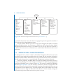
The Synthesis Lectures on Digital Circuits and Systems series is comprised of 50- to 100-page
books targeted for audience members with a wide-ranging background. The Lectures include topics
that are of interest to students, professionals, and researchers in the area of design and analysis of
digital circuits and systems. Each Lecture is self-contained and focuses on the background
information required to understand the subject matter and practical case studies that illustrate
applications. The format of a Lecture is structured such that each will be devoted to a specific topic
in digital circuits and systems rather than a larger overview of several topics such as that found in a
comprehensive handbook. The Lectures cover both well-established areas as well as newly
developed or emerging material in digital circuits and systems design and analysis.
Arduino Microcontroller: Processing for Everyone! Part I
Steven F. Barrett
2010
Digital System Verification: A Combined Formal Methods and Simulation Framework
Lun Li and Mitchell A. Thornton
2010
Progress in Applications of Boolean Functions
Tsutomu Sasao and Jon T. Butler
2009
Embedded Systems Design with the Atmel AVR Microcontroller: Part II
Steven F. Barrett
2009
Embedded Systems Design with the Atmel AVR Microcontroller: Part I
Steven F. Barrett
2009
Embedded Systems Interfacing for Engineers using the Freescale HCS08 Microcontroller
II: Digital and Analog Hardware Interfacing
Douglas H. Summerville
2009
iv
Designing Asynchronous Circuits using NULL Convention Logic (NCL)
Scott C. Smith and Jia Di
2009
Embedded Systems Interfacing for Engineers using the Freescale HCS08 Microcontroller
I: Assembly Language Programming
Douglas H.Summerville
2009
Developing Embedded Software using DaVinci & OMAP Technology
B.I. (Raj) Pawate
2009
Mismatch and Noise in Modern IC Processes
Andrew Marshall
2009
Asynchronous Sequential Machine Design and Analysis: A Comprehensive Development
of the Design and Analysis of Clock-Independent State Machines and Systems
Richard F. Tinder
2009
An Introduction to Logic Circuit Testing
Parag K. Lala
2008
Pragmatic Power
William J. Eccles
2008
Multiple Valued Logic: Concepts and Representations
D. Michael Miller and Mitchell A. Thornton
2007
Finite State Machine Datapath Design, Optimization, and Implementation
Justin Davis and Robert Reese
2007
Atmel AVR Microcontroller Primer: Programming and Interfacing
Steven F. Barrett and Daniel J. Pack
2007
Pragmatic Logic
William J. Eccles
2007
v
PSpice for Filters and Transmission Lines
Paul Tobin
2007
PSpice for Digital Signal Processing
Paul Tobin
2007
PSpice for Analog Communications Engineering
Paul Tobin
2007
PSpice for Digital Communications Engineering
Paul Tobin
2007
PSpice for Circuit Theory and Electronic Devices
Paul Tobin
2007
Pragmatic Circuits: DC and Time Domain
William J. Eccles
2006
Pragmatic Circuits: Frequency Domain
William J. Eccles
2006
Pragmatic Circuits: Signals and Filters
William J. Eccles
2006
High-Speed Digital System Design
Justin Davis
2006
Introduction to Logic Synthesis using Verilog HDL
Robert B.Reese and Mitchell A.Thornton
2006
Microcontrollers Fundamentals for Engineers and Scientists
Steven F. Barrett and Daniel J. Pack
2006
Copyright © 2010 by Morgan & Claypool
All rights reserved. No part of this publication may be reproduced, stored in a retrieval system, or transmitted in
any form or by any means—electronic, mechanical, photocopy, recording, or any other except for brief quotations in
printed reviews, without the prior permission of the publisher.
Arduino Microcontroller: Processing for Everyone! Part I
Steven F. Barrett
www.morganclaypool.com
ISBN: 9781608454372
ISBN: 9781608454389
paperback
ebook
DOI 10.2200/S00280ED1V01Y201005DCS028
A Publication in the Morgan & Claypool Publishers series
SYNTHESIS LECTURES ON DIGITAL CIRCUITS AND SYSTEMS
Lecture #28
Series Editor: Mitchell A. Thornton, Southern Methodist University
Series ISSN
Synthesis Lectures on Digital Circuits and Systems
Print 1932-3166 Electronic 1932-3174
Arduino Microcontroller
Processing for Everyone!
Part I
Steven F. Barrett
University of Wyoming, Laramie, WY
SYNTHESIS LECTURES ON DIGITAL CIRCUITS AND SYSTEMS #28
M
&C
Morgan
& cLaypool publishers
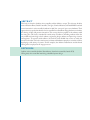
ABSTRACT
This book is about the Arduino microcontroller and the Arduino concept. The visionary Arduino
team of Massimo Banzi, David Cuartielles,Tom Igoe, Gianluca Martino, and David Mellis launched
a new innovation in microcontroller hardware in 2005, the concept of open source hardware. Their
approach was to openly share details of microcontroller-based hardware design platforms to stimulate
the sharing of ideas and promote innovation. This concept has been popular in the software world
for many years. This book is intended for a wide variety of audiences including students of the fine
arts, middle and senior high school students, engineering design students, and practicing scientists
and engineers. To meet this wide audience, the book has been divided into sections to satisfy the
need of each reader. The book contains many software and hardware examples to assist the reader in
developing a wide variety of systems. For the examples, the Arduino Duemilanove and the Atmel
ATmega328 is employed as the target processor.
KEYWORDS
Arduino microcontroller, Arduino Duemilanove, Atmel microcontroller, Atmel AVR,
ATmega328, microcontroller interfacing, embedded systems design
ix
Contents
Preface . . . . . . . . . . . . . . . . . . . . . . . . . . . . . . . . . . . . . . . . . . . . . . . . . . . . . . . . . . . . . . . . . . . . . xiii
1
Getting Started . . . . . . . . . . . . . . . . . . . . . . . . . . . . . . . . . . . . . . . . . . . . . . . . . . . . . . . . . . . . . . 1
1.1
Overview . . . . . . . . . . . . . . . . . . . . . . . . . . . . . . . . . . . . . . . . . . . . . . . . . . . . . . . . . . . . . . . . . . 1
1.2
Getting Started . . . . . . . . . . . . . . . . . . . . . . . . . . . . . . . . . . . . . . . . . . . . . . . . . . . . . . . . . . . . .1
1.3
Arduino Duemilanove . . . . . . . . . . . . . . . . . . . . . . . . . . . . . . . . . . . . . . . . . . . . . . . . . . . . . . 3
1.3.1 Arduino host processor — the ATmega328
1.4
3
Example: Autonomous Maze Navigating Robot . . . . . . . . . . . . . . . . . . . . . . . . . . . . . . . 4
1.4.1 Structure chart
6
1.4.2 UML activity diagrams
8
1.4.3 Arduino Duemilanove Systems
9
1.5
Arduino open source schematic . . . . . . . . . . . . . . . . . . . . . . . . . . . . . . . . . . . . . . . . . . . . . . 9
1.6
Other Arduino-based platforms . . . . . . . . . . . . . . . . . . . . . . . . . . . . . . . . . . . . . . . . . . . . . . 9
1.7
Extending the hardware features of the Arduino platform . . . . . . . . . . . . . . . . . . . . . . .9
1.8
Arduino Software . . . . . . . . . . . . . . . . . . . . . . . . . . . . . . . . . . . . . . . . . . . . . . . . . . . . . . . . . 12
1.9
Arduino Duemilanove/ATmega328 hardware features . . . . . . . . . . . . . . . . . . . . . . . . . 13
1.9.1 Memory
13
1.9.2 Port System
1.9.3 Internal Systems
15
16
1.10 Summary . . . . . . . . . . . . . . . . . . . . . . . . . . . . . . . . . . . . . . . . . . . . . . . . . . . . . . . . . . . . . . . . . 19
1.11 References . . . . . . . . . . . . . . . . . . . . . . . . . . . . . . . . . . . . . . . . . . . . . . . . . . . . . . . . . . . . . . . . 19
1.12 Chapter Problems . . . . . . . . . . . . . . . . . . . . . . . . . . . . . . . . . . . . . . . . . . . . . . . . . . . . . . . . . 19
2
Programming . . . . . . . . . . . . . . . . . . . . . . . . . . . . . . . . . . . . . . . . . . . . . . . . . . . . . . . . . . . . . . . 21
2.1
Overview . . . . . . . . . . . . . . . . . . . . . . . . . . . . . . . . . . . . . . . . . . . . . . . . . . . . . . . . . . . . . . . . . 21
2.2
The Big Picture . . . . . . . . . . . . . . . . . . . . . . . . . . . . . . . . . . . . . . . . . . . . . . . . . . . . . . . . . . . 22
x
2.3
Anatomy of a Program . . . . . . . . . . . . . . . . . . . . . . . . . . . . . . . . . . . . . . . . . . . . . . . . . . . . . 22
2.3.1 Comments
24
2.3.2 Include files
25
2.3.3 Functions
25
2.3.4 Program constants
28
2.3.5 Interrupt handler definitions
2.3.6 Variables
29
2.3.7 Main program
2.4
30
Fundamental programming concepts . . . . . . . . . . . . . . . . . . . . . . . . . . . . . . . . . . . . . . . . 30
2.4.1 Operators
30
2.4.2 Programming constructs
2.4.3 Decision processing
2.5
29
34
36
Arduino Development Environment . . . . . . . . . . . . . . . . . . . . . . . . . . . . . . . . . . . . . . . . 39
2.5.1 Background
39
2.5.2 Arduino Development Environment overview
2.5.3 Sketchbook concept
40
41
2.5.4 Arduino software, libraries, and language references
41
2.6
Application 1: Robot IR sensor . . . . . . . . . . . . . . . . . . . . . . . . . . . . . . . . . . . . . . . . . . . . . 42
2.7
Application 2: Art piece illumination system . . . . . . . . . . . . . . . . . . . . . . . . . . . . . . . . . 47
2.8
Summary . . . . . . . . . . . . . . . . . . . . . . . . . . . . . . . . . . . . . . . . . . . . . . . . . . . . . . . . . . . . . . . . . 47
2.9
References . . . . . . . . . . . . . . . . . . . . . . . . . . . . . . . . . . . . . . . . . . . . . . . . . . . . . . . . . . . . . . . . 48
2.10 Chapter Problems . . . . . . . . . . . . . . . . . . . . . . . . . . . . . . . . . . . . . . . . . . . . . . . . . . . . . . . . . 49
3
Embedded Systems Design . . . . . . . . . . . . . . . . . . . . . . . . . . . . . . . . . . . . . . . . . . . . . . . . . . 51
3.1
What is an embedded system? . . . . . . . . . . . . . . . . . . . . . . . . . . . . . . . . . . . . . . . . . . . . . . 51
3.2
Embedded system design process . . . . . . . . . . . . . . . . . . . . . . . . . . . . . . . . . . . . . . . . . . . 52
3.2.1 Project Description
3.2.2 Background Research
3.2.3 Pre-Design
3.2.4 Design
52
52
54
54
3.2.5 Implement Prototype
56
CONTENTS
3.2.6 Preliminary Testing
56
3.2.7 Complete and Accurate Documentation
4
57
3.3
Example: Blinky 602A autonomous maze navigating robot system design . . . . . . . 57
3.4
Application: Control algorithm for the Blinky 602A Robot . . . . . . . . . . . . . . . . . . . . 60
3.5
Summary . . . . . . . . . . . . . . . . . . . . . . . . . . . . . . . . . . . . . . . . . . . . . . . . . . . . . . . . . . . . . . . . . 71
3.6
References . . . . . . . . . . . . . . . . . . . . . . . . . . . . . . . . . . . . . . . . . . . . . . . . . . . . . . . . . . . . . . . . 71
3.7
Chapter Problems . . . . . . . . . . . . . . . . . . . . . . . . . . . . . . . . . . . . . . . . . . . . . . . . . . . . . . . . . 72
Serial Communication Subsystem . . . . . . . . . . . . . . . . . . . . . . . . . . . . . . . . . . . . . . . . . . . . 73
4.1
Overview . . . . . . . . . . . . . . . . . . . . . . . . . . . . . . . . . . . . . . . . . . . . . . . . . . . . . . . . . . . . . . . . . 73
4.2
Serial Communications . . . . . . . . . . . . . . . . . . . . . . . . . . . . . . . . . . . . . . . . . . . . . . . . . . . . 74
4.3
Serial Communication Terminology . . . . . . . . . . . . . . . . . . . . . . . . . . . . . . . . . . . . . . . . . 74
4.4
Serial USART . . . . . . . . . . . . . . . . . . . . . . . . . . . . . . . . . . . . . . . . . . . . . . . . . . . . . . . . . . . . 75
4.4.1 System Overview
4.5
4.6
76
System Operation and Programming using Arduino Development
Environment features . . . . . . . . . . . . . . . . . . . . . . . . . . . . . . . . . . . . . . . . . . . . . . . . . . . . . . 80
System Operation and Programming in C . . . . . . . . . . . . . . . . . . . . . . . . . . . . . . . . . . . 83
4.6.1 Serial Peripheral Interface—SPI
85
4.7
SPI Programming in the Arduino Development Environment . . . . . . . . . . . . . . . . . 88
4.8
SPI Programming in C . . . . . . . . . . . . . . . . . . . . . . . . . . . . . . . . . . . . . . . . . . . . . . . . . . . . 89
4.9
Two-wire Serial Interface—TWI . . . . . . . . . . . . . . . . . . . . . . . . . . . . . . . . . . . . . . . . . . . 90
4.10 Application 1: SD/MMC card module extension via the USART . . . . . . . . . . . . . . 90
4.11 Application 2: Programming the Arduino Duemilanove ATmega328 via the
ISP . . . . . . . . . . . . . . . . . . . . . . . . . . . . . . . . . . . . . . . . . . . . . . . . . . . . . . . . . . . . . . . . . . . . . . 93
4.11.1 Programming Procedure
93
4.12 Summary . . . . . . . . . . . . . . . . . . . . . . . . . . . . . . . . . . . . . . . . . . . . . . . . . . . . . . . . . . . . . . . . . 95
4.13 References . . . . . . . . . . . . . . . . . . . . . . . . . . . . . . . . . . . . . . . . . . . . . . . . . . . . . . . . . . . . . . . . 96
4.14 Chapter Problems . . . . . . . . . . . . . . . . . . . . . . . . . . . . . . . . . . . . . . . . . . . . . . . . . . . . . . . . . 96
Author’s Biography . . . . . . . . . . . . . . . . . . . . . . . . . . . . . . . . . . . . . . . . . . . . . . . . . . . . . . . . . . 97
Index . . . . . . . . . . . . . . . . . . . . . . . . . . . . . . . . . . . . . . . . . . . . . . . . . . . . . . . . . . . . . . . . . . . . . . . 99
xi
Preface
This book is about the Arduino microcontroller and the Arduino concept. The visionary
Arduino team of Massimo Banzi, David Cuartielles, Tom Igoe, Gianluca Martino, and David Mellis
launched a new innovation in microcontroller hardware in 2005, the concept of open source hardware.
There approach was to openly share details of microcontroller-based hardware design platforms to
stimulate the sharing of ideas and innovation. This concept has been popular in the software world
for many years.
This book is written for a number of audiences. First, in keeping with the Arduino concept,
the book is written for practitioners of the arts (design students, artists, photographers, etc.) who may
need processing power in a project but do not have an in depth engineering background. Second, the
book is written for middle school and senior high school students who may need processing power
for a school or science fair project. Third, we write for engineering students who require processing
power for their senior design project but do not have the background in microcontroller-based applications commonly taught in electrical and computer engineering curricula. Finally, the book provides
practicing scientists and engineers an advanced treatment of the Atmel AVR microcontroller.
APPROACH OF THE BOOK
To encompass such a wide range of readers, we have divided the book into several portions to address
the different readership. Chapters 1 through 2 are intended for novice microcontroller users. Chapter
1 provides a review of the Arduino concept, a description of the Arduino Duemilanove development
board, and a brief review of the features of the Duemilanove’s host processor, the Atmel ATmega 328
microcontroller. Chapter 2 provides an introduction to programming for the novice programmer.
Chapter 2 also introduces the Arduino Development Environment and how to program sketches.
It also serves as a good review for the seasoned developer.
Chapter 3 provides an introduction to embedded system design processes. It provides a systematic, step-by-step approach on how to design complex systems in a stress free manner.
Chapters 4 through 8 provide detailed engineering information on the ATmega328 microcontroller and advanced interfacing techniques. These chapters are intended for engineering students
and practicing engineers. However, novice microcontroller users will find the information readable
and well supported with numerous examples.
The final chapter provides a variety of example applications for a wide variety of skill levels.
xiv
PREFACE
ACKNOWLEDGMENTS
A number of people have made this book possible. I would like to thank Massimo Banzi of the
Arduino design team for his support and encouragement in writing the book. I would also like to
thank Joel Claypool of Morgan & Claypool Publishers who has supported a number of writing
projects of Daniel Pack and I over the last several years. He also provided permission to include
portions of background information on the Atmel line of AVR microcontrollers in this book from
several of our previous projects. I would also like to thank Sparkfun Electronics of Boulder, Colorado;
Atmel Incorporated; the Arduino team; and ImageCraft of Palo Alto, California for use of pictures
and figures used within the book.
I would like to dedicate this book to my close friend and writing partner Dr. Daniel Pack,
Ph.D., P.E. Daniel elected to “sit this one out” because of a thriving research program in unmanned
aerial vehicles (UAVs). Much of the writing is his from earlier Morgan & Claypool projects. In 2000,
Daniel suggested that we might write a book together on microcontrollers. I had always wanted to
write a book but I thought that’s what other people did. With Daniel’s encouragement we wrote
that first book (and six more since then). Daniel is a good father, good son, good husband, brilliant
engineer, a work ethic second to none, and a good friend. To you good friend I dedicate this book. I
know that we will do many more together.
Finally, I would like to thank my wife and best friend of many years, Cindy.
Laramie, Wyoming, May 2010
Steve Barrett
1
CHAPTER
1
Getting Started
Objectives: After reading this chapter, the reader should be able to the following:
• Describe the Arduino concept of open source hardware.
• Diagram the layout of the Arduino Duemilanove processor board.
• Name and describe the different features aboard the Arduino Duemilanove processor board.
• Discuss the features and functions of the ATmega328.
• List alternate Arduino processing boards.
• Describe how to extend the hardware features of the Arduino processor.
• Download, configure, and successfully execute a test program using the Arduino software.
1.1
OVERVIEW
Welcome to the world of Arduino! The Arduino concept of open source hardware was developed
by the visionary Arduino team of Massimo Banzi, David Cuartilles, Tom Igoe, Gianluca Martino,
and David Mellis in Ivrea, Italy. The team’s goal was to develop a line of easy-to-use microcontroller
hardware and software such that processing power would be readily available to everyone.
In keeping with the Arduino concept, this book is intended for a wide variety of readers. For
those wanting a quick exposure to an Arduino microcontroller board and its easy-to-use software,
Chapters 1 and 2 are for you. If you need to tap into some of the other features of the processing
power of the ATmega328 host microcontroller, Chapters 3 through 8 are for you.
In keeping with the Arduino open source spirit, you will find a plethora of hardware and
software examples throughout the book. I hope you enjoy reading the book, and I also hope you will
find it a useful resource in developing Arduino-based projects.
1.2
GETTING STARTED
This chapter is devoted to getting you quickly up and operating with an Arduino-based hardware
platform. To get started using an Arduino-based processor, you will need the following hardware
and software.
• an Arduino-based hardware processing platform,
2
1. GETTING STARTED
• an Arduino compatible power supply, and
• the Arduno software.
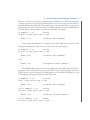
Arduino hardware. Throughout the book, we will be using the Arduino Duemilanove board.
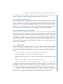
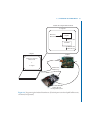
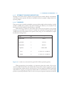
A starter’s kit for this platform is available from SparkFun Electronics of Boulder, CO for approximately US$60. The starter kit is illustrated in Figure 1.1. The kit is equipped with the processing
board, a USB cable to program the board from a host PC, a small breadboard to prototype external
hardware, jumper wires, and several external components. Later in the chapter, we will discuss other
Arduino-based processor kits.
Figure 1.1: Arduino Duemilanove starter kit. (Used with permission from SparkFun Electronics.)
Power supply. The Arduino processing board may be powered from the USB port during
project development. However, it is highly recommended that an external power supply be employed.
1.3. ARDUINO DUEMILANOVE
This will allow developing projects beyond the limited current capability of the USB port. SparkFun
Electronics recommends a power supply from 7-12 VDC with a 2.1 mm center positive plug. A
power supply of this type is readily available from a number of electronic parts supply companies.
For example, the Jameco #133891 power supply is a 9 VDC model rated at 300 mA and equipped
with a 2.1 mm center positive plug. It is available for under US$10.
Arduino software. You will also need the Arduino software called the Arduino Development
Environment. It is available as a free download from the Arduino homepage (www.arduino.cc). In
the Application section at the end of this chapter, we describe how to load the software and drivers
and get a sample program operating on the Arduino Duemilanove board.
In the next several sections, we provide information on the layout and capabilities of the
Arduino Duemilanove board and its host the Atmel ATmega328 processor. We also discuss other
Arduino-based processing boards and how to extend the features of the Arduino Duemilanove board
using the shield concept.
1.3
ARDUINO DUEMILANOVE
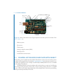
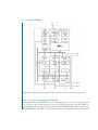
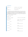
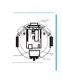
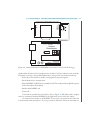
The Arduino Duemilanove processing board is illustrated in Figure 1.2. Working clockwise from
the left, the board is equipped with a USB connector to allow programming the processor from
a host PC. The board may also be programmed using In System Programming (ISP) techniques
discussed later in the book. A 6-pin ISP programming connector is on the opposite side of the board
from the USB connector.
The board is equipped with a USB-to-serial converter to allow compatibility between the host
PC and the serial communications systems aboard the ATmega328 processor. The Duemilanove is
also equipped with several small surface mount LEDs to indicate serial transmission (TX) and
reception (RX) and an extra LED for project use. The header strip at the top of the board provides
access for an analog reference signal, pulse width modulation (PWM) signals, digital input/output
(I/O), and serial communications. The header strip at the bottom of the board provides analog
inputs for the analog-to-digital (ADC) system and power supply terminals. Finally, the external
power supply connector is provided at the bottom left corner of the board. The top and bottom
header strips conveniently mate with an Arduino shield (to be discussed shortly) to extend the
features of the host processor.
1.3.1
ARDUINO HOST PROCESSOR — THE ATMEGA328
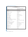
The host processor for the Arduino Duemilanove is the Atmel Atmega328. The “328” is a 28 pin,
8-bit microcontroller. The architecture is based on the Reduced Instruction Set Computer (RISC)
concept which allows the processor to complete 20 million instructions per second (MIPS) when
operating at 20 MHz!
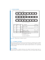
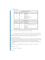
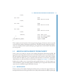
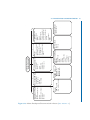
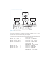
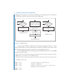
The “328” is equipped with a wide variety of features as shown in Figure 1.3. The features
may be conveniently categorized into the following systems:
3
1. GETTING STARTED
se
ria
lc
om
M
PW
PW
M
m
re
fe
re
nc
e
digital I/O
USB-to-serial LED
converter
TX LED
RX LED
an
al
og
4
timebase
LED power
indicator
switch
USB
connector
(to PC)
ISP programming
connector
power supply
connector
(7-12 VDC)
power supply
terminals
analog inputs
Figure 1.2: Arduino Duemilanove layout. (Figure adapted and used with permission of Arduino Team
(www.arduino.cc).)
• Memory system,
• Port system,
• Timer system,
• Analog-to-digital converter (ADC),
• Interrupt system,
• and the Serial communications.
1.4
EXAMPLE: AUTONOMOUS MAZE NAVIGATING ROBOT
Before taking a more in depth look at the Arduino Duemilanove systems, let’s see how these systems
would be used in an application. Graymark (www.graymarkint.com) manufacturers many low-cost,
excellent robot platforms. In this example, we will modify the Blinky 602A robot to be controlled
by the Arduino Duemilanove.
The Blinky 602A kit contains the hardware and mechanical parts to construct a line following
robot. The processing electronics for the robot consists of analog circuitry. The robot is controlled
by two 3 VDC motors which independently drive a left and right wheel. A third non-powered drag
wheel provides tripod stability for the robot.
5
1.4. EXAMPLE: AUTONOMOUS MAZE NAVIGATING ROBOT
Memory System
- 32K byte, ISP
programmable flash
- 1K byte, byte
addressable EEPROM
- 2K byte RAM
Arduino Duemilanove
Serial Communications
- Serial USART
- Serial peripheral interface
- Two wire interface (TWI)
Interrupt System
- 26 total interrupts
- 2 external pin interrupts
Analog-to-digital converter
- 6 channel 10-bit ADC
(PDIP)
hosted on the
ATmega328
Timer System
- Two 8-bit timer/counter
- One 16-bit timer/counter
- Six PWM channels
Port System
- 14 digital I/O pins
-- 6 provide PWM
- 6 analog input pins
Figure 1.3: Arduino Duemilanove systems.
6
1. GETTING STARTED
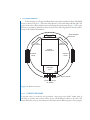
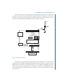
In this example, we will equip the Blinky 602A robot platform with three Sharp GP12D IR
sensors as shown in Figure 1.4. The robot will be placed in a maze with white reflective walls. The
goal is for the robot to detect wall placement and navigate through the maze. (Figure 1.5.) The robot
will not be provided any information about the maze. The control algorithm for the robot will be
hosted on the Arduino Duemilanove.
Sharp GP2D12
IR sensor
Center
IR sensor
Right
IR sensor
Left
IR sensor
Arduino
Duemilanove
powered
wheel
powered
wheel
prototype
area
turn signals
tripod drag wheel
for stability
Figure 1.4: Blinky robot layout.
1.4.1
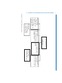
STRUCTURE CHART
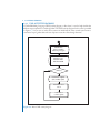
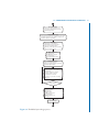
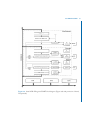
A structure chart is a visual tool used to partition a large project into “doable” smaller parts. It
also helps to visualize what systems will be used to control different features of the robot. The
arrows within the structure chart indicate the data flow between different portions of the program
1.4. EXAMPLE: AUTONOMOUS MAZE NAVIGATING ROBOT
Figure 1.5: Blinky robot navigating maze.
controlling the robot. The structure chart for the robot project is provided in Figure 1.6. As you
can see, the robot has three main systems: the motor control system, the sensor system, and the
digital input/output system. These three systems interact with the main control algorithm to allow
the robot to autonomously (by itself ) navigate through the maze by sensing and avoiding walls.
determine_robot
_action
sensor
data
robot
action
motor_control
desired
motor
action
PWM_left
left
motor
PWM_right
right
motor
digital
ADC
ch for
conv
input/output
conv
data
ADC
Initialize
ReadADC
left
turn
signal
left
IR sensor
middle
IR sensor
right
IR sensor
Figure 1.6: Blinky robot structure diagram.
running
lights
right
turn
signal
7
8
1. GETTING STARTED
1.4.2
UML ACTIVITY DIAGRAMS
A Unified Modeling Language (UML) activity diagram, or flow chart, is a tool to help visualize the
different steps required for a control algorithm. The UML activity diagram for the robot is provided
in Figure 1.7. As you can see, after robot systems are initialized, the robot control system enters a
continuous loop to gather data and issue outputs to steer the robot through the maze.
include files
global variables
function prototypes
initialize ports
initialize ADC
initialize PWM
while(1)
read sensor outputs
(left, middle, right)
determine robot
action
issue motor
control signals
Figure 1.7: Robot UML activity diagram.
1.5. ARDUINO OPEN SOURCE SCHEMATIC
1.4.3
ARDUINO DUEMILANOVE SYSTEMS
The three IR sensors (left, middle, and right) are mounted on the leading edge of the robot to detect
maze walls.The output from the sensors is fed to three ADC channels.The robot motors will each be
driven by a pulse width modulation (PWM) channel. The Arduino Duemilanove is interfaced to the
motors via a transistor with enough drive capability to handle the maximum current requirements of
the motor. The robot will be powered by a 9 VDC battery which is fed to a 5 VDC voltage regulator.
We discuss the details of the interface electronics in a later chapter.
From this example, you can see how different systems aboard the Arduino Duemilanove may
be used to control different features aboard the Blinky robot. In the next several sections, we present
information on the Arduino Duemilanove processor board and software.
1.5
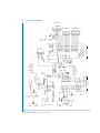
ARDUINO OPEN SOURCE SCHEMATIC
The entire line of Arduino products is based on the visionary concept of open source hardware and
software. That is, hardware and software developments are openly shared among users to stimulate
new ideas and advance the Arduino concept. In keeping with the Arduino concept, the Arduino
team openly shares the schematic of the Arduino Duemilanove processing board. Reference Figure
1.8.
1.6
OTHER ARDUINO-BASED PLATFORMS
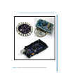
There is a wide variety of Arduino-based platforms.The platforms may be purchased from SparkFun
Electronics, Boulder, CO (www.sparkfun.com). Figure 1.9 provides a representative sample. Shown
on the left is the Arduino Lily Pad equipped with ATmega168 processor. A version of the Lily Pad
equipped with the ATmega328 will be released soon. This processing board can actually be worn
and is washable. It was designed to be sewn onto fabric.
In the bottom center figure is the Arduino Mega equipped with ATmega1280 processor. This
processing board is equipped with 54 digital input/output pins, 14 pulse width modulation pins, 16
analog inputs, and four channels of serial communication capability. In the upper right is the Arduio
Stamp. This small, but powerful processing board is equipped with ATmega168 processor.
1.7
EXTENDING THE HARDWARE FEATURES OF THE
ARDUINO PLATFORM
Additional features and external hardware may be added to selected Arduino platforms by using a
daughter card concept. The daughter card is called an Arduino Shield as shown in Figure 1.10. The
shield mates with the header pins on the Arduino board. The shield provides a small fabrication
area, a processor reset button, and a general use pushbutton and two light emitting diodes (LEDs).
This concludes the review of the Arduino Duemilanove and related Arduino-based processing
boards. In the next section, we discuss how to download and obtain the latest Arduino software.
9
1. GETTING STARTED
USB-to-USART
converter
ATmega328
P
O
R
T
D
P
O
R
T
C
P
O
R
T
B
10
Figure 1.8: Arduino Duemilanove open source schematic. (Figure adapted and used with permission of
the Arduino Team (www.arduino.cc).)
1.7. EXTENDING THE HARDWARE FEATURES OF THE ARDUINO PLATFORM
Figure 1.9: Arduino variants. (Used with permission from SparkFun Electronics.)
11
12
1. GETTING STARTED
Figure 1.10: Arduino shield. (Used with permission from SparkFun Electronics.)
1.8
ARDUINO SOFTWARE
In the next chapter, we will discuss how to program the Arduino Duemilanove processing board
using the Arduino Development Environment. It is essential that you download and get the software
operating correctly before proceeding to the next chapter.
1.9. ARDUINO DUEMILANOVE/ATMEGA328 HARDWARE FEATURES
13
The Arduino homepage (www.arduino.cc) contains detailed instructions on how to download the software, load the USB drivers, and get a sample program operating on the Arduino
Duemilanove processing board. Due to limited space, these instructions will not be duplicated here.
The reader is encouraged to visit the Arduino webpage and get the software up and operating at this
time.
This completes a brief overview of the Arduino hardware and software. In the next section,
we provide a more detailed overview of the hardware features of the Arduino processor, the Atmel
ATmega328.
1.9
ARDUINO DUEMILANOVE/ATMEGA328 HARDWARE
FEATURES
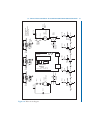
As previously mentioned, the Arduino Duemilanove’s processing power is provided by the ATmega328. The pin out diagram and block diagram for this processor are provided in Figures 1.11
and 1.12. In this section, we provide additional detail on the systems aboard the processor.
Figure 1.11: ATmega328 pin out. (Figure used with permission of Atmel, Incorporated.)
1.9.1
MEMORY
The ATmega328 is equipped with three main memory sections: flash electrically erasable programmable read only memory (EEPROM), static random access memory (SRAM), and byteaddressable EEPROM for data storage. We discuss each memory component in turn.
14
1. GETTING STARTED
Figure 1.12: ATmega328 block diagram. (Figure used with permission of Atmel, Incorporated.)
1.9.1.1 In-System Programmable Flash EEPROM
Bulk programmable flash EEPROM is used to store programs. It can be erased and programmed
as a single unit. Also, should a program require a large table of constants, it may be included as a
global variable within a program and programmed into flash EEPROM with the rest of the program.
Flash EEPROM is nonvolatile meaning memory contents are retained when microcontroller power
1.9. ARDUINO DUEMILANOVE/ATMEGA328 HARDWARE FEATURES
15
is lost. The ATmega328 is equipped with 32K bytes of onboard reprogrammable flash memory. This
memory component is organized into 16K locations with 16 bits at each location.
1.9.1.2 Byte-Addressable EEPROM
Byte-addressable memory is used to permanently store and recall variables during program execution.
It too is nonvolatile. It is especially useful for logging system malfunctions and fault data during
program execution. It is also useful for storing data that must be retained during a power failure but
might need to be changed periodically. Examples where this type of memory is used are found in
applications to store system parameters, electronic lock combinations, and automatic garage door
electronic unlock sequences. The ATmega328 is equipped with 1024 bytes of EEPROM.
1.9.1.3 Static Random Access Memory (SRAM)
Static RAM memory is volatile. That is, if the microcontroller loses power, the contents of SRAM
memory are lost. It can be written to and read from during program execution. The ATmega328
is equipped with 2K bytes of SRAM. A small portion of the SRAM is set aside for the general
purpose registers used by the processor and also for the input/output and peripheral subsystems
aboard the microcontroller. A complete ATmega328 register listing and accompanying header file
is provided in Appendices A and B, respectively. During program execution, RAM is used to store
global variables, support dynamic memory allocation of variables, and to provide a location for the
stack (to be discussed later).
1.9.2
PORT SYSTEM
The Atmel ATmega328 is equipped with four, 8-bit general purpose, digital input/output (I/O)
ports designated PORTA, PORTB, PORTC, and PORTD. All of these ports also have alternate
functions which will be described later. In this section, we concentrate on the basic digital I/O port
features.
As shown in Figure 1.13, each port has three registers associated with it
• Data Register PORTx —- used to write output data to the port.
• Data Direction Register DDRx —- used to set a specific port pin to either output (1) or input
(0).
• Input Pin Address PINx —- used to read input data from the port.
Figure 1.13(b) describes the settings required to configure a specific port pin to either input
or output. If selected for input, the pin may be selected for either an input pin or to operate in the
high impedance (Hi-Z) mode. In Hi-Z mode, the input appears as high impedance to a particular
pin. If selected for output, the pin may be further configured for either logic low or logic high.
Port pins are usually configured at the beginning of a program for either input or output and
their initial values are then set. Usually all eight pins for a given port are configured simultaneously.
We discuss how to configure port pins and how to read/write to them in the next chapter.
16
1. GETTING STARTED
Port x Data Register - PORTx
7
Port x Data Direction Register - DDRx
0
7
Port x Input Pins Address - PINx
0
7
0
a) port associated registers
DDxn
PORTxn
I/O
Comment
Pullup
0
0
input
Tri-state (Hi-Z)
No
0
1
input
source current if externally pulled low
Yes
1
0
output Output Low (Sink)
No
1
1
output Output High (Source)
No
x: port designator (A, B, C, D)
n: pin designator (0 - 7)
b) port pin configuration
Figure 1.13: ATmega328 port configuration registers.
1.9.3
INTERNAL SYSTEMS
In this section, we provide a brief overview of the internal features of the ATmega328. It should be
emphasized that these features are the internal systems contained within the confines of the microcontroller chip. These built-in features allow complex and sophisticated tasks to be accomplished by
the microcontroller.
1.9.3.1 Time Base
The microcontroller is a complex synchronous state machine. It responds to program steps in a
sequential manner as dictated by a user-written program. The microcontroller sequences through
1.9. ARDUINO DUEMILANOVE/ATMEGA328 HARDWARE FEATURES
17
a predictable fetch-decode-execute sequence. Each unique assembly language program instruction
issues a series of signals to control the microcontroller hardware to accomplish instruction related
operations.
The speed at which a microcontroller sequences through these actions is controlled by a precise
time base called the clock. The clock source is routed throughout the microcontroller to provide a
time base for all peripheral subsystems. The ATmega328 may be clocked internally using a userselectable resistor capacitor (RC) time base or it may be clocked externally. The RC internal time
base is selected using programmable fuse bits. We will discuss how to do this in the application
section of this chapter. You may choose an internal fixed clock operating frequency of 1, 2, 4 or 8
MHz.
To provide for a wider range of frequency selections an external time source may be used. The
external time sources, in order of increasing accuracy and stability, are an external RC network, a
ceramic resonator, or a crystal oscillator. The system designer chooses the time base frequency and
clock source device appropriate for the application at hand.
1.9.3.2 Timing Subsystem
The ATmega328 is equipped with a complement of timers which allows the user to generate a
precision output signal, measure the characteristics (period, duty cycle, frequency) of an incoming
digital signal, or count external events. Specifically, the ATmega328 is equipped with two 8-bit
timer/counters and one 16-bit counter. We discuss the operation, programming, and application of
the timing system later in the book.
1.9.3.3 Pulse Width Modulation Channels
A pulse width modulated or PWM signal is characterized by a fixed frequency and a varying duty
cycle. Duty cycle is the percentage of time a repetitive signal is logic high during the signal period.
It may be formally expressed as:
duty cycle[%] = (on time/period) × (100%)
The ATmega328 is equipped with four pulse width modulation (PWM) channels. The PWM
channels coupled with the flexibility of dividing the time base down to different PWM subsystem
clock source frequencies allows the user to generate a wide variety of PWM signals: from relatively
high frequency low duty cycle signals to relatively low frequency high duty cycle signals.
PWM signals are used in a wide variety of applications including controlling the position of
a servo motor and controlling the speed of a DC motor. We discuss the operation, programming,
and application of the PWM system later in the book.
1.9.3.4 Serial Communications
The ATmega328 is equipped with a host of different serial communication subsystems including
the Universal Synchronous and Asynchronous Serial Receiver and Transmitter (USART), the serial
18
1. GETTING STARTED
peripheral interface (SPI), and the Two-wire Serial Interface. What all of these systems have in
common is the serial transmission of data. In a serial communications transmission, scheme data is
sent a single bit at a time from transmitter to receiver.
Serial USART The serial USART is used for full duplex (two way) communication between
a receiver and transmitter. This is accomplished by equipping the ATmega328 with independent
hardware for the transmitter and receiver. The USART is typically used for asynchronous communication. That is, there is not a common clock between the transmitter and receiver to keep them
synchronized with one another. To maintain synchronization between the transmitter and receiver,
framing start and stop bits are used at the beginning and end of each data byte in a transmission
sequence.
The ATmega328 USART is quite flexible. It has the capability to be set to a variety of data
transmission rates known as the Baud (bits per second) rate. The USART may also be set for data
bit widths of 5 to 9 bits with one or two stop bits. Furthermore, the ATmega328 is equipped with
a hardware generated parity bit (even or odd) and parity check hardware at the receiver. A single
parity bit allows for the detection of a single bit error within a byte of data. The USART may
also be configured to operate in a synchronous mode. We discuss the operation, programming, and
application of the USART later in the book.
Serial Peripheral Interface—SPI The ATmega328 Serial Peripheral Interface (SPI) can also be
used for two-way serial communication between a transmitter and a receiver. In the SPI system,
the transmitter and receiver share a common clock source. This requires an additional clock line
between the transmitter and receiver but allows for higher data transmission rates as compared to
the USART.
The SPI may be viewed as a synchronous 16-bit shift register with an 8-bit half residing in
the transmitter and the other 8-bit half residing in the receiver. The transmitter is designated the
master since it is providing the synchronizing clock source between the transmitter and the receiver.
The receiver is designated as the slave. We discuss the operation, programming, and application of
the SPI later in the book.
Two-wire Serial Interface—TWI The TWI subsystem allows the system designer to network a
number of related devices (microcontrollers, transducers, displays, memory storage, etc.) together
into a system using a two wire interconnecting scheme. The TWI allows a maximum of 128 devices
to be connected together. Each device has its own unique address and may both transmit and receive
over the two wire bus at frequencies up to 400 kHz. This allows the device to freely exchange
information with other devices in the network within a small area. We discuss the TWI system later
in the book.
1.9.3.5 Analog to Digital Converter—ADC
The ATmega328 is equipped with an eight channel analog to digital converter (ADC) subsystem.
The ADC converts an analog signal from the outside world into a binary representation suitable for
1.10. SUMMARY
19
use by the microcontroller. The ATmega328 ADC has 10 bit resolution. This means that an analog
voltage between 0 and 5 V will be encoded into one of 1024 binary representations between (000)16
and (3F F )16 . This provides the ATmega328 with a voltage resolution of approximately 4.88 mV.
We discuss the operation, programming, and application of the ADC later in the book.
1.9.3.6 Interrupts
The normal execution of a program step follows a designated sequence of instructions. However,
sometimes this normal sequence of events must be interrupted to respond to high priority faults
and status both inside and outside the microcontroller. When these higher priority events occur, the
microcontroller must temporarily suspend normal operation and execute event specific actions called
an interrupt service routine. Once the higher priority event has been serviced, the microcontroller
returns and continues processing the normal program.
The ATmega328 is equipped with a complement of 26 interrupt sources.Two of the interrupts
are provided for external interrupt sources while the remaining interrupts support the efficient operation of peripheral subsystems aboard the microcontroller. We discuss the operation, programming,
and application of the interrupt system later in the book.
1.10 SUMMARY
In this chapter, we have provided an overview of the Arduino concept of open source hardware.
This was followed by a description of the Arduino Duemilanove processor board powered by the
ATmega328. An overview of ATmega328 systems followed. We then investigated various processing
boards in the Arduino line and concluded with brief guidelines on how to download and run the
Arduino software environment.
1.11 REFERENCES
• SparkFun Electronics, 6175 Longbow Drive, Suite 200, Boulder, CO 80301
(www.sparkfun.com)
• Arduino homepage (www.arduino.cc)
• Atmel 8-bit AVR Microcontroller with 4/8/16/32K Bytes In-System Programmable Flash, ATmega48PA, 88PA, 168PA, 328P data sheet: 8161D-AVR-10/09, Atmel Corporation, 2325
Orchard Parkway, San Jose, CA 95131.
1.12 CHAPTER PROBLEMS
1. Describe in your own words the Arduino open source concept.
2. Sketch a block diagram of the ATmega328 and its associated systems. Describe the function
of each system.
20
1. GETTING STARTED
3. What is the purpose of a structure chart?
4. What is the purpose of a UML activity diagram?
5. Describe the different types of memory components within the ATmega328. Describe applications for each memory type.
6. Describe the three different register types associated with each port.
7. How may the features of the Arduino Demilanove be extended?
21
CHAPTER
2
Programming
Objectives: After reading this chapter, the reader should be able to do the following:
• Describe the key components of a program.
• Specify the size of different variables within the C programming language.
• Define the purpose of the main program.
• Explain the importance of using functions within a program.
• Write functions that pass parameters and return variables.
• Describe the function of a header file.
• Discuss different programming constructs used for program control and decision processing.
• Describe the key features of the Arduino Development Environment.
• Describe what features of the Arduino Development Environment ease the program development process.
• List the programming support information available at the Arduino home page.
• Write programs for use on the Arduino Duemilanove processing board.
2.1
OVERVIEW
To the novice, programming a microcontroller may appear mysterious, complicated, overwhelming,
and difficult. When faced with a new task, one often does not know where to start. The goal of
this chapter is to provide a tutorial on how to begin programming. We will use a top-down design
approach. We begin with the “big picture” of the chapter followed by an overview of the major
pieces of a program. We then discuss the basics of the C programming language. Only the most
fundamental concepts will be covered. We then discuss the Ardunio Development Environment and
how it may be used to develop a program for the Arduino Duemilanove processor board.Throughout
the chapter, we provide examples and also provide references to a number of excellent references.
22
2. PROGRAMMING
2.2
THE BIG PICTURE
We begin with the big picture of how to program the Arduino Duemilanove as shown in Figure
2.1. This will help provide an overview of how chapter concepts fit together. It also introduces terms
used in writing, editing, compiling, loading and executing a program.
Most microcontrollers are programmed with some variant of the C programming language.
The C programming language provides a nice balance between the programmer’s control of the
microcontroller hardware and time efficiency in programming writing.
As you can see in Figure 2.1, the compiler software is hosted on a computer separate from
the Arduino Duemilanove. The job of the compiler is to transform the program provided by the
program writer (filename.c and filename.h) into machine code (filename.hex) suitable for loading
into the processor.
Once the source files (filename.c and filename.h) are provided to the compiler, the compiler
executes two steps to render the machine code. The first step is the compilation process. Here the
program source files are transformed into assembly code (filename.asm). If the program source files
contains syntax errors, the compiler reports these to the user. An assembly language program is not
generated until the syntax errors have been corrected.
The assembly language source file (filename.asm) is then passed to the assembler. The assembler transforms the assembly language source file (filename.asm) to machine code (filename.asm)
suitable for loading to the Arduino Duemilanove.
The Arduino Development Environment provides a user friendly interface to aid in program
development, transformation to machine code, and loading into the Arduino Duemilanove. The
Arduino Duemilanove may also be programmed using the In System Programming (ISP) features
of the Atmel AVR STK500 Starter Kit and Development System. We discuss these procedures in
a later chapter.
In the next section, we will discuss the components of a C program. In a later section, we
discuss the user friendly features of the Arduino Development Environment.
2.3
ANATOMY OF A PROGRAM
Programs written for a microcontroller have a fairly repeatable format. Slight variations exist but
many follow the format provided.
//Comments containing program information
// - file name:
// - author:
// - revision history:
// - compiler setting information:
// - hardware connection description to microcontroller pins
// - program description
2.3. ANATOMY OF A PROGRAM
23
Arduino Development Environment
C compiler
filename.c
filename.h
compiler
filename.asm
assembler
filename.hex
filename.eep
computer
Arduino Development
Environment
Arduino
Duemilanove
USB
ISP
or
C compiler
filename.hex
filename.eep
ISP
Atmel AVR STK500
Starter Kit and
Development System
Figure 2.1: Programming the Arduino Duemilanove. (Used with permission from SparkFun Electronics,
and Atmel, Incorporated.)
24
2. PROGRAMMING
//include files
#include<file_name.h>
//function prototypes
A list of functions and their format used within the program
//program constants
#define
TRUE
1
#define
FALSE 0
#define
ON
1
#define
OFF
0
//interrupt handler definitions
Used to link the software to hardware interrupt features
//global variables
Listing of variables used throughout the program
//main program
void main(void)
{
body of the main program
}
//function definitions
A detailed function body and definition
for each function used within the program
Let’s take a closer look at each piece.
2.3.1
COMMENTS
Comments are used throughout the program to document what and how things were accomplished
within a program. The comments help you reconstruct your work at a later time. Imagine that you
wrote a program a year ago for a project. You now want to modify that program for a new project.
The comments will help you remember the key details of the program.
Comments are not compiled into machine code for loading into the microcontroller.Therefore,
the comments will not fill up the memory of your microcontroller. Comments are indicated using
2.3. ANATOMY OF A PROGRAM
25
double slashes (//). Anything from the double slashes to the end of a line is then considered a
comment. A multi-line comment can be constructed using a /∗ at the beginning of the comment
and a ∗/ at the end of the comment.
At the beginning of the program, comments may be extensive. Comments may include some
of the following information:
• file name
• program author
• revision history or a listing of the key changes made to the program
• compiler setting information
• hardware connection description to microcontroller pins
• program description
2.3.2
INCLUDE FILES
Often you need to add extra files to your project besides the main program. For example, most
compilers require a “personality file” on the specific microcontroller that you are using. This file is
provided with the compiler and provides the name of each register used within the microcontroller.
It also provides the link between a specific register’s name within software and the actual register
location within hardware. These files are typically called header files and their name ends with a “.h”.
Within the C compiler there will also be other header files to include in your program such as the
“math.h” file when programming with advanced math functions.
To include header files within a program, the following syntax is used:
//include files
#include<file_name1.h>
#include<file_name2.h>
In an upcoming section, we see how the Arduino Development Environment makes it quite
easy to include a header file within a program.
2.3.3
FUNCTIONS
In the next chapter, we discuss in detail the top down design, bottom up implementation approach to
designing microcontroller based systems. In this approach, a microcontroller based project including
both hardware and software is partitioned into systems, subsystems, etc.The idea is to take a complex
project and break it into doable pieces with a defined action.
26
2. PROGRAMMING
We use the same approach when writing computer programs. At the highest level is the main
program which calls functions that have a defined action. When a function is called, program control
is released from the main program to the function. Once the function is complete, program control
reverts back to the main program.
Functions may in turn call other functions as shown in Figure 2.2. This approach results in a
collection of functions that may be reused over and over again in various projects. Most importantly,
the program is now subdivided into doable pieces, each with a defined action. This makes writing
the program easier but also makes it much easier to modify the program since every action is in a
known location.
void main(void)
{
:
function1( );
void function1(void)
{
:
:
}
function2( );
:
}
void function2(void)
{
:
}
Figure 2.2: Function calling.
There are three different pieces of code required to properly configure and call the function:
• the function prototype,
• the function call, and
• the function body.
Function prototypes are provided early in the program as previously shown in the program
template. The function prototype provides the name of the function and any variables required by
the function and any variable returned by the function.
The function prototype follows this format:
return_variable
function_name(required_variable1, required_variable2);
2.3. ANATOMY OF A PROGRAM
27
If the function does not require variables or sends back a variable the word “void” is placed in
the variable’s position.
The function call is the code statement used within a program to execute the function. The
function call consists of the function name and the actual arguments required by the function. If the
function does not require arguments to be delivered to it for processing, the parenthesis containing
the variable list is left empty.
The function call follows this format:
function_name(required_variable1, required_variable2);
A function that requires no variables follows this format:
function_name( );
When the function call is executed by the program, program control is transferred to the
function, the function is executed, and program control is then returned to the portion of the
program that called it.
The function body is a self-contained “mini-program.” The first line of the function body
contains the same information as the function prototype: the name of the function, any variables
required by the function, and any variable returned by the function. The last line of the function
contains a “return” statement. Here a variable may be sent back to the portion of the program that
called the function. The processing action of the function is contained within the open ({) and
close brackets (}). If the function requires any variables within the confines of the function, they are
declared next. These variable are referred to as local variables. The actions required by the function
follow.
The function prototype follows this format:
return_variable function_name(required_variable1, required_variable2)
{
//local variables required by the function
unsigned int variable1;
unsigned char variable2;
//program statements required by the function
//return variable
return return_variable;
}
Example: In this example, we describe how to configure the ports of the microcontroller to act
as input or output ports. Briefly, associated with each port is a register called the data direction register
(DDR). Each bit in the DDR corresponds to a bit in the associated PORT. For example, PORTB
28
2. PROGRAMMING
has an associated data direction register DDRB. If DDRB[7] is set to a logic 1, the corresponding
port pin PORTB[7] is configured as an output pin. Similarly, if DDRB[7] is set to logic 0, the
corresponding port pin is configured as an input pin.
During some of the early steps of a program, a function is called to initialize the ports as input,
output, or some combination of both. This is illustrated in Figure 2.3.
//function prototypes
void initialize_ports(void);
//main function
void main(void)
{
:
initialize_ports( );
:
}
//function body
void initialize_ports(void)
{
DDRB = 0x00;
//initialize PORTB as input
PORTB = 0x00;
DDRC = 0xFF;
PORTC = 0x00;
//initialize PORTC as output
//set pins to logic 0
DDRD = 0xFF;
PORTD = 0x00;
}
//initialize PORTD as output
//set pins to logic 0
Figure 2.3: Configuring ports.
2.3.4
PROGRAM CONSTANTS
The #define statement is used to associate a constant name with a numerical value in a program. It
can be used to define common constants such as pi. It may also be used to give terms used within a
program a numerical value. This makes the code easier to read. For example, the following constants
may be defined within a program:
//program constants
#define
TRUE
1
#define
FALSE 0
#define
ON
1
#define
OFF
0
2.3. ANATOMY OF A PROGRAM
2.3.5
29
INTERRUPT HANDLER DEFINITIONS
Interrupts are functions that are written by the programmer but usually called by some hardware
event during system operation. We discuss interrupts and how to properly configure them in an
upcoming chapter.
2.3.6
VARIABLES
There are two types of variables used within a program: global variables and local variables. A global
variable is available and accessible to all portions of the program. Whereas, a local variable is only
known and accessible within the function where it is declared.
When declaring a variable in C, the number of bits used to store the operator is also specified.
In Figure 2.4, we provide a list of common C variable sizes used with the ImageCraft ICC AVR
compiler. The size of other variables such as pointers, shorts, longs, etc. are contained in the compiler
documentation [ImageCraft].
Size
Range
unsigned char
1
0..255
signed char
1
-128..127
unsigned int
2
0..65535
signed int
2
-32768..32767
float
4
+/-1.175e-38.. +/-3.40e+38
double
4
+/-1.175e-38.. +/-3.40e+38
Type
Figure 2.4: C variable sizes used with the ImageCraft ICC AVR compiler [ImageCraft].
When programming microcontrollers, it is important to know the number of bits used to
store the variable and also where the variable will be assigned. For example, assigning the contents
of an unsigned char variable, which is stored in 8-bits, to an 8-bit output port will have a predictable
result. However, assigning an unsigned int variable, which is stored in 16-bits, to an 8-bit output
port does not provide predictable results. It is wise to insure your assignment statements are balanced
30
2. PROGRAMMING
for accurate and predictable results. The modifier “unsigned” indicates all bits will be used to specify
the magnitude of the argument. Signed variables will use the left most bit to indicate the polarity
(±) of the argument.
A global variable is declared using the following format provided below. The type of the
variable is specified, followed by its name, and an initial value if desired.
//global variables
unsigned int loop_iterations = 6;
2.3.7
MAIN PROGRAM
The main program is the hub of activity for the entire program. The main program typically consists
of program steps and function calls to initialize the processor followed by program steps to collect
data from the environment external to the microcontroller, process the data and make decisions, and
provide external control signals back to the environment based on the data collected.
2.4
FUNDAMENTAL PROGRAMMING CONCEPTS
In the previous section, we covered many fundamental concepts. In this section we discuss operators,
programming constructs, and decision processing constructs to complete our fundamental overview
of programming concepts.
2.4.1
OPERATORS
There are a wide variety of operators provided in the C language. An abbreviated list of common
operators are provided in Figures 2.5 and 2.6. The operators have been grouped by general category.
The symbol, precedence, and brief description of each operator are provided.The precedence column
indicates the priority of the operator in a program statement containing multiple operators. Only
the fundamental operators are provided. For more information on this topic, see Barrett and Pack
in the Reference section at the end of the chapter.
2.4.1.1 General operations
Within the general operations category are brackets, parenthesis, and the assignment operator. We
have seen in an earlier example how bracket pairs are used to indicate the beginning and end of the
main program or a function. They are also used to group statements in programming constructs and
decision processing constructs. This is discussed in the next several sections.
The parenthesis is used to boost the priority of an operator. For example, in the mathematical
expression 7 x 3 + 10, the multiplication operation is performed before the addition since it has
a higher precedence. Parenthesis may be used to boost the precedence of the addition operation. If
we contain the addition operation within parenthesis 7 x (3 + 10), the addition will be performed
before the multiplication operation and yield a different result from the earlier expression.
2.4. FUNDAMENTAL PROGRAMMING CONCEPTS
General
Symbol
Precedence
Description
{}
1
Brackets, used to group program statements
()
1
Parenthesis, used to establish precedence
=
12
Assignment
Arithmetic Operations
Symbol
Precedence
Description
*
3
Multiplication
/
3
Division
+
4
Addition
-
4
Subtraction
Logical Operations
Symbol
Precedence
Description
<
6
Less than
<=
6
Less than or equal to
>
6
Greater
>=
6
Greater than or equal to
==
!=
7
7
Equal to
Not equal to
&&
9
Logical AND
||
10
Logical OR
Figure 2.5: C operators. (Adapted from [Barrett and Pack]).
31
32
2. PROGRAMMING
Bit Manipulation Operations
Symbol
Precedence
<<
5
Shift left
>>
5
Shift right
&
8
Bitwise AND
^
|
8
8
Bitwise exclusive OR
Bitwise OR
Description
Unary Operations
Symbol
Precedence
Description
!
2
Unary negative
~
2
One’s complement (bit-by-bit inversion)
++
2
Increment
-type(argument)
2
Decrement
2
Casting operator (data type conversion)
Figure 2.6: C operators (continued). (Adapted from [Barrett and Pack]).
The assignment operator (=) is used to assign the argument(s) on the right-hand side of an
equation to the left-hand side variable. It is important to insure that the left and the right-hand side
of the equation have the same type of arguments. If not, unpredictable results may occur.
2.4.1.2 Arithmetic operations
The arithmetic operations provide for basic math operations using the various variables described
in the previous section. As described in the previous section, the assignment operator (=) is used to
assign the argument(s) on the right-hand side of an equation to the left-hand side variable.
Example: In this example, a function returns the sum of two unsigned int variables passed to
the function.
unsigned int
{
unsigned int
sum_two(unsigned int variable1, unsigned int variable2)
sum;
sum = variable1 + variable2;
return sum;
2.4. FUNDAMENTAL PROGRAMMING CONCEPTS
33
}
2.4.1.3 Logical operations
The logical operators provide Boolean logic operations.They can be viewed as comparison operators.
One argument is compared against another using the logical operator provided.The result is returned
as a logic value of one (1, true, high) or zero (0 false, low). The logical operators are used extensively
in program constructs and decision processing operations to be discussed in the next several sections.
2.4.1.4 Bit manipulation operations
There are two general types of operations in the bit manipulation category: shifting operations and
bitwise operations. Let’s examine several examples:
Example: Given the following code segment, what will the value of variable2 be after execution?
unsigned char
unsigned char
variable1 = 0x73;
variable2;
variable2 = variable1 << 2;
Answer: Variable “variable1” is declared as an eight bit unsigned char and assigned the hexadecimal value of (73)16 . In binary this is (0111_0011)2 . The << 2 operator provides a left shift of
the argument by two places. After two left shifts of (73)16 , the result is (cc)16 and will be assigned
to the variable “variable2.”
Note that the left and right shift operation is equivalent to multiplying and dividing the
variable by a power of two.
The bitwise operators perform the desired operation on a bit-by-bit basis. That is, the least
significant bit of the first argument is bit-wise operated with the least significant bit of the second
argument and so on.
Example: Given the following code segment, what will the value of variable3 be after execution?
unsigned char
unsigned char
unsigned char
variable1 = 0x73;
variable2 = 0xfa;
variable3;
variable3 = variable1 & variable2;
Answer: Variable “variable1” is declared as an eight bit unsigned char and assigned the hexadecimal value of (73)16 . In binary, this is (0111_0011)2 . Variable “variable2” is declared as an eight
bit unsigned char and assigned the hexadecimal value of (f a)16 . In binary, this is (1111_1010)2 .
34
2. PROGRAMMING
The bitwise AND operator is specified. After execution variable “variable3,” declared as an eight bit
unsigned char, contains the hexadecimal value of (72)16 .
2.4.1.5 Unary operations
The unary operators, as their name implies, require only a single argument.
For example, in the following code segment, the value of the variable “i” is incremented. This
is a shorthand method of executing the operation “i = i + 1; ”
unsigned int
i;
i++;
Example: It is not uncommon in embedded system design projects to have every pin on a
microcontroller employed. Furthermore, it is not uncommon to have multiple inputs and outputs
assigned to the same port but on different port input/output pins. Some compilers support specific
pin reference. Another technique that is not compiler specific is bit twiddling. Figure 2.7 provides
bit twiddling examples on how individual bits may be manipulated without affecting other bits using
bitwise and unary operators.The information provided here was extracted from the ImageCraft ICC
AVR compiler documentation [ImageCraft].
Syntax
Description
a|b
bitwise or
a&b
bitwise and
a^b
bitwise exclusive or
PORTA ^= 0x80; // flip bit 7
~a
bitwise complement
PORTA &= ~0x80; // turn off bit 7
Example
PORTA |= 0x80; // turn on bit 7 (msb)
if ((PINA & 0x81) == 0) // check bit 7 and bit 0
Figure 2.7: Bit twiddling [ImageCraft].
2.4.2
PROGRAMMING CONSTRUCTS
In this section, we discuss several methods of looping through a piece of code. We will examine the
“for” and the “while” looping constructs.
The for loop provides a mechanism for looping through the same portion of code a fixed
number of times. The for loop consists of three main parts:
2.4. FUNDAMENTAL PROGRAMMING CONCEPTS
35
• loop initiation,
• loop termination testing, and
• the loop increment.
In the following code fragment the for loop is executed ten times.
unsigned int
loop_ctr;
for(loop_ctr = 0; loop_ctr < 10; loop_ctr++)
{
//loop body
}
The for loop begins with the variable “loop_ctr” equal to 0. During the first pass through the
loop, the variable retains this value. During the next pass through the loop, the variable “loop_ctr”
is incremented by one. This action continues until the “loop_ctr” variable reaches the value of ten.
Since the argument to continue the loop is no longer true, program execution continues after the
close bracket for the for loop.
In the previous example, the for loop counter was incremented at the beginning of each loop
pass. The “loop_ctr” variable can be updated by any amount. For example, in the following code
fragment the “loop_ctr” variable is increased by three for every pass of the loop.
unsigned int
loop_ctr;
for(loop_ctr = 0; loop_ctr < 10; loop_ctr=loop_ctr+3)
{
//loop body
}
The “loop_ctr” variable may also be initialized at a high value and then decremented at the
beginning of each pass of the loop.
unsigned int
loop_ctr;
for(loop_ctr = 10; loop_ctr > 0; loop_ctr--)
{
//loop body
}
36
2. PROGRAMMING
As before, the “loop_ctr” variable may be decreased by any numerical value as appropriate for
the application at hand.
The while loop is another programming construct that allows multiple passes through a
portion of code. The while loop will continue to execute the statements within the open and close
brackets while the condition at the beginning of the loop remains logically true. The code snapshot
below will implement a ten iteration loop. Note how the “loop_ctr” variable is initialized outside of
the loop and incremented within the body of the loop. As before, the variable may be initialized to
a greater value and then decremented within the loop body.
unsigned int
loop_ctr;
loop_ctr = 0;
while(loop_ctr < 10)
{
//loop body
loop_ctr++;
}
Frequently, within a microcontroller application, the program begins with system initialization
actions. Once initialization activities are complete, the processor enters a continuous loop. This may
be accomplished using the following code fragment.
while(1)
{
}
2.4.3
DECISION PROCESSING
There are a variety of constructs that allow decision making. These include the following:
• the if statement,
• the if–else construct,
• the if–else if–else construct, and the
• switch statement.
The if statement will execute the code between an open and close bracket set should the
condition within the if statement be logically true.
Example: To help develop the algorithm for steering the Blinky 602A robot through a maze,
a light emitting diode (LED) is connected to PORTB pin 1 on the ATmega328. The robot’s center
2.4. FUNDAMENTAL PROGRAMMING CONCEPTS
37
IR sensor is connected to an analog-to-digital converter at PORTC, pin 1. The IR sensor provides
a voltage output that is inversely proportional to distance of the sensor from the maze wall. It is
desired to illuminate the LED if the robot is within 10 cm of the maze wall. The sensor provides an
output voltage of 2.5 VDC at the 10 cm range. The following if statement construct will implement
this LED indicator. We provide the actual code to do this later in the chapter.
if (PORTC[1] > 2.5)
//Center
IR sensor voltage greater than 2.5 VDC
{
PORTB = 0x02;
//illuminate LED on PORTB[1]
}
In the example provided, there is no method to turn off the LED once it is turned on. This
will require the else portion of the construct as shown in the next code fragment.
if (PORTC[1] > 2.5)
//Center
IR sensor voltage greater than 2.5 VDC
{
PORTB = 0x02;
//illuminate LED on PORTB[1]
}
else
{
PORTB = 0x00;
//extinguish the LED on PORTB[1]
}
The if–else if—else construct may be used to implement a three LED system. In this example, the left, center, and right IR sensors are connected to analog-to-digital converter channels on
PORTC pins 2, 1, and 0, respectively. The LED indicators are connected to PORTB pins 2, 1, and
0. The following code fragment implements this LED system.
if (PORTC[2] > 2.5)
//Left IR
sensor voltage greater than 2.5 VDC
{
PORTB = 0x04;
//illuminate LED on PORTB[2]
}
else if (PORTC[1] > 2.5)
//Center
IR sensor voltage greater than 2.5 VDC
{
PORTB = 0x02;
//illuminate the LED on PORTB[1]
}
else if (PORTC[0] > 2.5)
//Right
IR sensor voltage greater than 2.5 VDC
38
2. PROGRAMMING
{
PORTB = 0x01;
}
else
{
PORTB = 0x00;
}
//illuminate the LED on PORTB[0]
//no walls sensed within 10 cm
//extinguish LEDs
The switch statement is used when multiple if-else conditions exist. Each possible condition is
specified by a case statement. When a match is found between the switch variable and a specific case
entry, the statements associated with the case are executed until a break statement is encountered.
Example: Suppose eight pushbutton switches are connected to PORTD. Each switch will
implement a different action. A switch statement may be used to process the multiple possible
decisions as shown in the following code fragment.
void read_new_input(void)
{
new_PORTD = PIND;
if(new_PORTD != old_PORTD)
switch(new_PORTD)
{
case 0x01:
//check for status change PORTD
//process change in PORTD input
//PD0
//PD0 related actions
break;
case 0x02:
//PD1
//PD1 related actions
break;
case 0x04:
//PD2
//PD2 related actions
break;
case 0x08:
//PD3
//PD3 related actions
break;
case 0x10:
//PD4
//PD4 related actions
2.5. ARDUINO DEVELOPMENT ENVIRONMENT
39
break;
case 0x20:
//PD5
//PD5 related actions
break;
case 0x40:
//PD6
//PD6 related actions
break;
case 0x80:
//PD7
//PD7 related actions
break;
default:;
}
}
old_PORTD=new_PORTD;
}
//all other cases
//end switch(new_PORTD)
//end if new_PORTD
//update PORTD
That completes our brief overview of the C programming language. In the next section, we provide
an overview of the Arduino Development Environment. You will see how this development tool provides a user-friendly method of quickly developing code applications for the Arduino Duemilanove
processing board.
2.5
ARDUINO DEVELOPMENT ENVIRONMENT
In this section, we provide an overview of the Arduino Development Environment (ADE). We
begin with some background information about the ADE and then review its user friendly features.
We then introduce the sketchbook concept and provide a brief overview of the built-in software
features within the ADE. Our goal is to provide a brief introduction to the features. All Arduino
related features are well-documented on the Arduino homepage (www.arduino.cc). We will not
duplicate this excellent source of material but merely provide pointers to it. In later chapters, we
review the different systems aboard the Arduino Duemilanove processing board and show how that
system may be controlled using the ADE built-in features.
2.5.1
BACKGROUND
The first version of the Arduino Development Environment was released in August 2005. It was
developed at the Interaction Design Institute in Ivrea, Italy to allow students the ability to quickly put
40
2. PROGRAMMING
processing power to use in a wide variety of projects. Since that time, newer versions incorporating
new features, have been released on a regular basis [www.arduino.cc].
At its most fundamental level, the Arduino Development Environment is a user friendly
interface to allow one to quickly write, load, and execute code on a microcontroller. A barebones
program need only consist of a setup() and loop() function.The Arduino Development Environment
adds the other required pieces such as header files and the main program construct. The ADE is
written in Java and has its origins in the Processor programming language and the Wiring Project
[www.arduino.cc].
In the next several sections, we introduce the user interface and its large collection of user
friendly tools. We also provide an overview of the host of built-in C and C++ software functions
that allows the project developer to quickly put the features of the Arduino Duemilanove processing
board to work for them.
2.5.2
ARDUINO DEVELOPMENT ENVIRONMENT OVERVIEW
The Arduino Development Environment is illustrated in Figure 2.8.The ADE contains a text editor,
a message area for displaying status, a text console, a tool bar of common functions, and an extensive
menuing system. The ADE also provides a user friendly interface to the Arduino Duemilanove
which allows for a quick upload of code. This is possible because the Arduino Duemilanove is
equipped with a bootloader program.
sketch_feb15a | Arduino 0017
File
Edit
Sketch
Tools
Help
sketch_feb15a
Figure 2.8: Arduino Development Environment [www.arduino.cc].
2.5. ARDUINO DEVELOPMENT ENVIRONMENT
41
A close up of the Arduino toolbar is provided in Figure 2.9. The toolbar provides single button
access to the more commonly used menu features. Most of the features are self explanatory. The
“Upload to I/O Board” button compiles your code and uploads it to the Arduino Duemilanove. The
“Serial Monitor” button opens the serial monitor feature. The serial monitor feature allows text data
to be sent to and received from the Arduino Duemilanove. The serial monitor feature is halted with
the “Stop” button.
Open
Verify/Compile
Stop
New
Save
Upload to I/O board
Serial monitor
Figure 2.9: Arduino Development Environment buttons.
2.5.3
SKETCHBOOK CONCEPT
In keeping with a hardware and software platform for students of the arts, the Arduino environment
employs the concept of a sketchbook. An artist maintains their works in progress in a sketchbook.
Similarly, we maintain our programs within a sketchbook in the Arduino environment. Furthermore,
we refer to individual programs as sketches. An individual sketch within the sketchbook may be
accessed via the Sketchbook entry under the file tab.
2.5.4
ARDUINO SOFTWARE, LIBRARIES, AND LANGUAGE REFERENCES
The Arduino Development Environment has a number of built in features. Some of the features
may be directly accessed via the Arduino Development Environment drop down toolbar illustrated
in Figure 2.8. Provided in Figure 2.10 is a handy reference to show all of the available features.
The toolbar provides a wide variety of features to compose, compile, load and execute a sketch. We
illustrate how to use these features in the Application section later in the chapter.
Aside from the toolbar accessible features, the Arduino Development Environment contains
a number of built-in functions that allow the user to quickly construct a sketch. These built-in
functions are summarized in Figure 2.11. Complete documentation for these built-in features is
available at the Arduino homepage [www.arduino.cc]. This documentation is easily accessible via
the Help tab on the Arduino Development Environment toolbar. This documentation will not be
42
2. PROGRAMMING
Menu
File
- New
- Open
- Sketchbook
- Examples
- Close
- Save
- Save As
- Upload to I/O Board
- Page Setup
- Print
- Preferences
- Quit
Edit
- Undo
- Redo
- Cut
- Copy
- Copy for Forum
- Copy as HTML
- Paste
- Select All
- Comment/
Uncomment
- Increase Indent
- Decrease Indent
- Find
- Find Next
Sketch
- Verify/Compile
- Step
- Import Library
- Show Sketch Folder
- Add File
Tools
- Auto Format
- Archive Sketch
- Fix Encoding &
Reload
- Board
- Serial Port
- Burn Bootloader
Help
- Getting Started
- Environment
- Troubleshooting
- Reference
- Find in Reference
- Frequently Asked
Questions
- Visit Arduino.cc
- About Arduino
Figure 2.10: Arduino Development Environment menu [www.arduino.cc].
repeated here. Instead, we refer to these features at appropriate places throughout the remainder of
the book as we discuss related hardware systems.
Keep in mind the Arduino open source concept. Users throughout the world are constantly
adding new built-in features. As new features are added, they will be released in future Arduino
Development Environment versions. As an Arduino user, you too may add to this collection of
useful tools. In the next section, we illustrate how to use the Arduino Duemilanova board in several
applications.
2.6
APPLICATION 1: ROBOT IR SENSOR
To demonstrate how to construct a sketch in the Arduino Development Environment, we revisit
the robot IR sensor application provided earlier in the chapter. We also investigate the sketches’s
interaction with the Arduino Duemilanove processing board and external sensors and indicators.
We will use the robot project as an ongoing example throughout the remainder of the book.
Recall from Chapter 1, the Blinky 602A kit contains the hardware and mechanical parts to
construct a line following robot. In this example, we modify the robot platform by equipping it with
three Sharp GP12D IR sensors as shown in Figure 2.12. The sensors are available from SparkFun
Electronics (www.sparkfun.com). The sensors are mounted to a bracket constructed from thin
aluminum. Dimensions for the bracket are provided in the figure. Alternatively, the IR sensors may
be mounted to the robot platform using “L” brackets available from a local hardware store. In later
Application sections, we equip the robot with all three IR sensors. In this example, we equip the
robot with a single sensor and test its function as a proof of concept.
Sensors
- ADX3xx accelerometer
- Knock detector
- Memsic2125 two-axis
accelerometer
- Ping ultrasonic range
finder
Stepper Library
- Motor knob
Communication
- ASCII Table
- Dimmer
- Graph
- Physical pixel
- Virtual color mixer
- Serial call response
- Serial call response
ASCII
- Serial input
- MIDI
Liquid Crystal Display Servo Library
- Knob
Library
- Sweep
- Hello World
- Blink
- Cursor
- Display
- Text Direction
- Scroll
- Serial Input
- SetCursor
- Autoscroll
Control Structures
- If statement
- For loop
- Array
- While loop
- Switch case
- Switch case 2
EEPROM Library
- EEPROM clear
- EEPROM read
- EEPROM write
Analog Input/Output
- Analog Input
- Calibration
- Fading
- Smoothing
Display
- LED bar graph
- Row column scanning
Digital Input/Output
- Blink
- Blink without delay
- Button
- Button state change
- Debounce
- Melody
Arduino Environment
Built-in Programs
2.6. APPLICATION 1: ROBOT IR SENSOR
Figure 2.11: Arduino Development Environment built in features [www.arduino.cc].
43
44
2. PROGRAMMING
6
1-7/16
all holes 1/8
1/2
1/2
2
Figure 2.12: Blinky robot platform modified with three IR sensors.
1/2
2.6. APPLICATION 1: ROBOT IR SENSOR
45
The IR sensor provides a voltage output that is inversely proportional to the sensor distance
from the maze wall. It is desired to illuminate the LED if the robot is within 10 cm of the maze
wall. The sensor provides an output voltage of 2.5 VDC at the 10 cm range. The interface between
the IR sensor and the Arduino Duemilanove board is provided in Figure 2.13.
5 VDC
220
10K
3 21 0 9 8 76 5 4 32 1 0
1 1 1 1 DIGITAL
Arduino
Duemilanove
5VGnd
2N2222
Ground
ANALOG IN
0 123 4 5
R Y B
IR sensor
Figure 2.13: IR sensor interface.
The IR sensor’s power (red wire) and ground (black wire) connections are connected to the 5V
and Gnd pins on the Arduino Duemilanove board, respectively. The IR sensor’s output connection
(yellow wire) is connected to the ANALOG IN 5 pin on the Arduino Duemilanove board. The
LED circuit shown in the top right corner of the diagram is connected to the DIGITAL 0 pin on
the Arduino Duemilanove board. We discuss the operation of this circuit in the Interfacing chapter
later in the book.
46
2. PROGRAMMING
Earlier in the chapter, we provided a framework for writing the if-else statement to turn the
LED on and off. Here is the actual sketch to accomplish this.
//*************************************************************************
#define LED_PIN
0
//digital pin - LED connection
#define IR_sensor_pin 5
//analog pin - IR sensor
int IR_sensor_value;
void setup()
{
pinMode(LED_PIN, OUTPUT);
}
//declare variable for IR sensor value
//configure pin 0 for digital output
void loop()
{
//read analog output from IR sensor
IR_sensor_value = analogRead(IR_sensor_pin);
if(IR_sensor_value > 512)
{
digitalWrite(LED_PIN, HIGH);
}
else
{
digitalWrite(LED_PIN, LOW);
}
//0 to 1023 maps to 0 to 5 VDC
//turn LED on
//turn LED off
}
//************************************************************************
The sketch begins by providing names for the two Arduino Duemilanove board pins that will
be used in the sketch. This is not required but it makes the code easier to read. We define the pin
for the LED as “LED_PIN.” Any descriptive name may be used here. Whenever the name is used
within the sketch, the number “0” will be substituted for the name by the compiler.
After providing the names for pins, the next step is to declare any variables required by the
sketch. In this example, the output from the IR sensor will be converted from an analog to a digital
value using the built-in Arduino “analogRead” function. A detailed description of the function may
be accessed via the Help menu. It is essential to carefully review the support documentation for a
built-in Arduino function the first time it is used. The documentation provides details on variables
required by the function, variables returned by the function, and an explanation on function operation.
2.7. APPLICATION 2: ART PIECE ILLUMINATION SYSTEM
47
The “analogRead” function requires the pin for analog conversion variable passed to it and
returns the analog signal read as an integer value (int) from 0 to 1023. So, for this example, we
need to declare an integer value to receive the returned value. We have called this integer variable
“IR_sensor_value.”
Following the declaration of required variables are the two required functions for an Arduino
Duemilanove program: setup and loop. The setup function calls an Arduino built-in function, pinMode, to set the “LED_PIN” as an output pin. The loop function calls several functions to read the
current analog value on pin 5 (the IR sensor output) and then determine if the reading is above 512
(2.5 VDC). If the reading is above 2.5 VDC, the LED on DIGITAL pin 0 is illuminated, else it is
turned off.
After completing writing the sketch with the Arduino Development Environment, it must be
compiled and then uploaded to the Arduino Duemilanove board. These two steps are accomplished
using the “Sketch – Verify/Compile” and the “File – Upload to I/O Board” pull down menu selections.
In the next example, we adapt the IR sensor project to provide custom lighting for an art
piece.
2.7
APPLICATION 2: ART PIECE ILLUMINATION SYSTEM
My oldest son Jonny Barrett is a gifted artist based in Park City, Utah (www.
closertothesunfineartndesign.com). Although I own several of his pieces, my favorite one
is a painting he did during his early student days. The assignment was to paint your favorite place.
Jonny painted Lac Laronge, Saskatchewan as viewed through the window of a pontoon plane. Jonny,
his younger brother Graham, and I have gone on several fishing trips with friends to this very special
location. An image of the painting is provided in Figure 2.14.
The circuit and sketch provided in the earlier example may be slightly modified to provide
custom lighting for an art piece. The IR sensor could be used to detect the presence and position
of those viewing the piece. Custom lighting could then be activated by the Arduino Duemilanove
board via the DIGITAL output pins. In the Lac Laronge piece, lighting could be provided from
behind the painting using high intensity white LEDs. The intensity of the LEDs could be adjusted
by changing the value of the resistor is series with the LED. The lighting intensity could also be
varied based on the distance the viewer is from the painting. We cover the specifics in an upcoming
chapter.
2.8
SUMMARY
The goal of this chapter was to provide a tutorial on how to begin programming. We used a topdown design approach. We began with the “big picture” of the chapter followed by an overview
of the major pieces of a program. We then discussed the basics of the C programming language.
Only the most fundamental concepts were covered. We then discussed the Arduino Development
Environment and how it may be used to develop a program for the Arduino Duemilanove processor
48
2. PROGRAMMING
Figure 2.14: Lac Laronge, Saskatchewan. Image used with permission, Jonny Barrett, Closer to the Sun
Fine Art and Design, Park City, Utah. [www.closertothesunfineartndesign.com]
board. Throughout the chapter, we provided examples and also provided references to a number of
excellent references.
2.9
REFERENCES
• ImageCraft Embedded Systems C Development Tools, 706 Colorado Avenue, #10-88, Palo
Alto, CA, 94303, www.imagecraft.com
• S. F. Barrett and D.J. Pack, Embedded Systems Design and Applications with the 68HC12
and HCS12, Pearson Prentice Hall, 2005.
• Arduino homepage, www.arduino.cc
• Jonny Barrett, Closer to the Sun Fine Art and Design, Park City, UT,
www.closertothesunfineartndesign.com
2.10. CHAPTER PROBLEMS
49
• Barrett S, Pack D (2006) Microcontrollers Fundamentals for Engineers and Scientists. Morgan
and Claypool Publishers. DOI: 10.2200/S00025ED1V01Y200605DCS001
• Barrett S and Pack D (2008) Atmel AVR Microcontroller Primer Programming and Interfacing. Morgan and Claypool Publishers. DOI: 10.2200/S00100ED1V01Y200712DCS015
• Barrett S (2010) Embedded Systems Design with the Atmel AVR Microcontroller. Morgan
and Claypool Publishers. DOI: 10.2200/S00225ED1V01Y200910DCS025
2.10 CHAPTER PROBLEMS
1. Describe the steps in writing a sketch and executing it on an Arduino Duemilanove processing
board.
2. Describe the key portions of a C program.
3. Describe two different methods to program an Arduino Duemilanove processing board.
4. What is an include file?
5. What are the three pieces of code required for a program function?
6. Describe how to define a program constant.
7. Provide the C program statement to set PORTB pins 1 and 7 to logic one. Use bit-twiddling
techniques.
8. Provide the C program statement to reset PORTB pins 1 and 7 to logic zero. Use bit-twiddling
techniques.
9. What is the difference between a for and while loop?
10. When should a switch statement be used versus the if-then statement construct?
11. What is the serial monitor feature used for in the Arduino Development Environment?
12. Describe what variables are required and returned and the basic function of the following
built-in Arduino functions: Blink, Analog Input.
51
CHAPTER
3
Embedded Systems Design
Objectives: After reading this chapter, the reader should be able to do the following:
• Define an embedded system.
• List all aspects related to the design of an embedded system.
• Provide a step-by-step approach to embedded system design.
• Discuss design tools and practices related to embedded systems design.
• Apply embedded system design practices in the design of an Arduino-based microcontroller
system employing several interacting subsystems.
• Provide a detailed design for an autonomous maze navigating robot controlled by the Arduino
Duemilanove including hardware layout and interface, structure and UML activity diagrams,
and coded algorithm.
In Chapters 1 and 2, we provided an overview of the Arduino Duemilanove hardware and the
Arduino Development Environment to get you quickly up and operating with this user friendly processor. In the remainder of the book, we will take a second and detailed pass through this information.
This chapter provides a step-by-step methodical approach to designing advanced embedded system.
Chapters 4 through 7 take an advanced look at the serial communications systems, the analog-todigital converter system, the interrupt system, and the timing system. Chapter 8 provides detailed
information on how to interface a wide variety of peripheral devices to the Arduino Duemilanove
processor. Throughout these chapters, we show how the built-in features of the Arduino Development Environment may be employed in different applications.
In this chapter, we begin with a definition of just what is an embedded system. We then explore
the process of how to successfully (and with low stress) develop an embedded system prototype that
meets established requirements. We conclude the chapter with an extended example. The example
illustrates the embedded system design process in the development and prototype of the autonomous
maze navigating robot based on the Blinky 602A (www.graymarkint.com) controlled by the Arduino
Duemilanove processing board.
3.1
WHAT IS AN EMBEDDED SYSTEM?
An embedded system contains a microcontroller to accomplish its job of processing system inputs
and generating system outputs. The link between system inputs and outputs is provided by a coded
52
3. EMBEDDED SYSTEMS DESIGN
algorithm stored within the processor’s resident memory. What makes embedded systems design so
interesting and challenging is the design must also take into account the proper electrical interface
for the input and output devices, limited on-chip resources, human interface concepts, the operating
environment of the system, cost analysis, related standards, and manufacturing aspects [Anderson].
Through careful application of this material you will be able to design and prototype embedded
systems based on the Arduino microcontroller.
3.2
EMBEDDED SYSTEM DESIGN PROCESS
In this section, we provide a step-by-step approach to develop the first prototype of an embedded
system that will meet established requirements. There are many formal design processes that we
could study. We concentrate on the steps that are common to most. We purposefully avoid formal
terminology of a specific approach and instead concentrate on the activities that are accomplished as
a system prototype is developed. The design process we describe is illustrated in Figure 3.1 using a
Unified Modeling Language (UML) activity diagram. We discuss the UML activity diagrams later
in the chapter.
3.2.1
PROJECT DESCRIPTION
The goal of the project description step is to determine what the system is ultimately supposed to do.
To achieve this step you must thoroughly investigate what the system is supposed to do. Questions
to raise and answer during this step include but are not limited to the following:
• What is the system supposed to do?
• Where will it be operating and under what conditions?
• Are there any restrictions placed on the system design?
To answer these questions, the designer interacts with the client to ensure clear agreement
on what is to be done. If you are completing this project for yourself, you must still carefully and
thoughtfully complete this step. The establishment of clear, definable system requirements may
require considerable interaction between the designer and the client. It is essential that both parties
agree on system requirements before proceeding further in the design process. The final result of
this step is a detailed listing of system requirements and related specifications.
3.2.2
BACKGROUND RESEARCH
Once a detailed list of requirements has been established, the next step is to perform background
research related to the design. In this step, the designer will ensure they understand all requirements
and features required by the project. This will again involve interaction between the designer and the
client.The designer will also investigate applicable codes, guidelines, protocols, and standards related
to the project.This is also a good time to start thinking about the interface between different portions
3.2. EMBEDDED SYSTEM DESIGN PROCESS
Project Description
- What is the system supposed to do?
- Operating conditions and environment
- Formal requirements
Background Research
- Thoroughly understand desired requirements and features
- Determine applicable codes, guidelines, and protocols
- Determine interface requirements
Pre-Design
- Brainstorm possible solutions
- Thoroughly investigate alternatives
- Choose best possible solution
- Identify specific target microcontroller
- Choose a design approach
Employ Design Tools
- Structure chart
- UML activity diagram
- Circuit diagram
- Supplemental information
Implement Prototype
- Top down versus bottom up
- Develop low risk hardware test platform
- Software implementation
Preliminary Testing
- Develop test plan to insure requirements
have been met
- Test under anticipated conditions
- Test under abusive conditions
- Redo testing if errors found
- Test in low cost, low risk environment
- Full up test
yes
System design
need correction?
no
Complete and Accurate Documentation
- System description
- Requirements
- Structure chart
- UML activity diagram
- Circuit diagram
- Well-documented code
- Test plan
Deliver Prototype
Figure 3.1: Embedded system design process.
53
54
3. EMBEDDED SYSTEMS DESIGN
of the project particularly the input and output devices peripherally connected to the microcontroller.
The ultimate objective of this step is to have a thorough understanding of the project requirements,
related project aspects, and any interface challenges within the project.
3.2.3
PRE-DESIGN
The goal of the pre-design step is to convert a thorough understanding of the project into possible
design alternatives. Brainstorming is an effective tool in this step. Here, a list of alternatives is developed. Since an embedded system typically involves both hardware and/or software, the designer can
investigate whether requirements could be met with a hardware only solution or some combination
of hardware and software. Generally, speaking a hardware only solution executes faster; however, the
design is fixed once fielded. On the other hand, a software implementation provides flexibility and
a typically slower execution speed. Most embedded design solutions will use a combination of both
hardware and software to capitalize on the inherent advantages of each.
Once a design alternative has been selected, the general partition between hardware and
software can be determined. It is also an appropriate time to select a specific hardware device to
implement the prototype design. If a microcontroller technology has been chosen, it is now time to
select a specific controller. This is accomplished by answering the following questions:
• What microcontroller systems or features i.e., ADC, PWM, timer, etc.) are required by the
design?
• How many input and output pins are required by the design?
• What is the maximum anticipated operating speed of the microcontroller expected to be?
Recall from Chapter 1 there are a wide variety of Arduino-based microcontrollers available
to the designer.
3.2.4
DESIGN
With a clear view of system requirements and features, a general partition determined between
hardware and software, and a specific microcontroller chosen, it is now time to tackle the actual
design. It is important to follow a systematic and disciplined approach to design. This will allow
for low stress development of a documented design solution that meets requirements. In the design
step, several tools are employed to ease the design process. They include the following:
• Employing a top-down design, bottom up implementation approach,
• Using a structure chart to assist in partitioning the system,
• Using a Unified Modeling Language (UML) activity diagram to work out program flow, and
• Developing a detailed circuit diagram of the entire system.
3.2. EMBEDDED SYSTEM DESIGN PROCESS
55
Let’s take a closer look at each of these. The information provided here is an abbreviated
version of the one provided in “Microcontrollers Fundamentals for Engineers and Scientists.” The
interested reader is referred there for additional details and an indepth example [Barrett and Pack].
Top down design, bottom up implementation. An effective tool to start partitioning the
design is based on the techniques of top-down design, bottom-up implementation. In this approach,
you start with the overall system and begin to partition it into subsystems. At this point of the design,
you are not concerned with how the design will be accomplished but how the different pieces of
the project will fit together. A handy tool to use at this design stage is the structure chart. The
structure chart shows the hierarchy of how system hardware and software components will interact
and interface with one another. You should continue partitioning system activity until each subsystem
in the structure chart has a single definable function.
UML Activity Diagram. Once the system has been partitioned into pieces, the next step
in the design process is to start working out the details of the operation of each subsystem we
previously identified. Rather than beginning to code each subsystem as a function, we will work out
the information and control flow of each subsystem using another design tool: the Unified Modeling
Language (UML) activity diagram. The activity diagram is simply a UML compliant flow chart.
UML is a standardized method of documenting systems. The activity diagram is one of the many
tools available from UML to document system design and operation. The basic symbols used in a
UML activity diagram for a microcontroller based system are provided in Figure 3.2[Fowler].
Starting
Activity
Branch
Transfer
of Control
Final State
Action State
Figure 3.2: UML activity diagram symbols. Adapted from [source].
56
3. EMBEDDED SYSTEMS DESIGN
To develop the UML activity diagram for the system, we can use a top-down, bottom-up, or a
hybrid approach. In the top-down approach, we begin by modeling the overall flow of the algorithm
from a high level. If we choose to use the bottom-up approach, we would begin at the bottom of
the structure chart and choose a subsystem for flow modeling. The specific course of action chosen
depends on project specifics. Often, a combination of both techniques, a hybrid approach, is used.
You should work out all algorithm details at the UML activity diagram level prior to coding any
software. If you can not explain system operation at this higher level, first, you have no business
being down in the detail of developing the code. Therefore, the UML activity diagram should be of
sufficient detail so you can code the algorithm directly from it [Dale].
In the design step, a detailed circuit diagram of the entire system is developed. It will serve
as a roadmap to implement the system. It is also a good idea at this point to investigate available
design information relative to the project. This would include hardware design examples, software
code examples, and application notes available from manufacturers.
At the completion of this step, the prototype design is ready for implementation and testing.
3.2.5
IMPLEMENT PROTOTYPE
To successfully implement a prototype, an incremental approach should be followed. Again, the topdown design, bottom-up implementation provides a solid guide for system implementation. In an
embedded system design involving both hardware and software, the hardware system including the
microcontroller should be assembled first. This provides the software the required signals to interact
with. As the hardware prototype is assembled on a prototype board, each component is tested for
proper operation as it is brought online. This allows the designer to pinpoint malfunctions as they
occur.
Once the hardware prototype is assembled, coding may commence. As before, software should
be incrementally brought online. You may use a top down, bottom up, or hybrid approach depending
on the nature of the software. The important point is to bring the software online incrementally
such that issues can be identified and corrected early on.
It is highly recommended that low cost stand-in components be used when testing the software
with the hardware components. For example, push buttons, potentiometers, and LEDs may be used
as low cost stand-in component simulators for expensive input instrumentation devices and expensive
output devices such as motors. This allows you to insure the software is properly operating before
using it to control the actual components.
3.2.6
PRELIMINARY TESTING
To test the system, a detailed test plan must be developed. Tests should be developed to verify that
the system meets all of its requirements and also intended system performance in an operational
environment.The test plan should also include scenarios in which the system is used in an unintended
manner. As before a top-down, bottom-up, or hybrid approach can be used to test the system.
3.3. EXAMPLE: BLINKY 602A AUTONOMOUS MAZE NAVIGATING ROBOT SYSTEM DESIGN
Once the test plan is completed, actual testing may commence. The results of each test should
be carefully documented. As you go through the test plan, you will probably uncover a number of
run time errors in your algorithm. After you correct a run time error, the entire test plan must be
performed again. This ensures that the new fix does not have an unintended affect on another part
of the system. Also, as you process through the test plan, you will probably think of other tests that
were not included in the original test document. These tests should be added to the test plan. As
you go through testing, realize your final system is only as good as the test plan that supports it!
Once testing is complete, you might try another level of testing where you intentionally try
to “jam up” the system. In another words, try to get your system to fail by trying combinations of
inputs that were not part of the original design. A robust system should continue to operate correctly
in this type of an abusive environment. It is imperative that you design robustness into your system.
When testing on a low cost simulator is complete, the entire test plan should be performed again
with the actual system hardware. Once this is completed you should have a system that meets its
requirements!
3.2.7
COMPLETE AND ACCURATE DOCUMENTATION
With testing complete, the system design should be thoroughly documented. Much of the documentation will have already been accomplished during system development. Documentation will
include the system description, system requirements, the structure chart, the UML activity diagrams
documenting program flow, the test plan, results of the test plan, system schematics, and properly
documented code. To properly document code, you should carefully comment all functions describing their operation, inputs, and outputs. Also, comments should be included within the body of
the function describing key portions of the code. Enough detail should be provided such that code
operation is obvious. It is also extremely helpful to provide variables and functions within your code
names that describe their intended use.
You might think that a comprehensive system documentation is not worth the time or effort
to complete it. Complete documentation pays rich dividends when it is time to modify, repair, or
update an existing system. Also, well-documented code may be often reused in other projects: a
method for efficient and timely development of new systems.
3.3
EXAMPLE: BLINKY 602A AUTONOMOUS MAZE
NAVIGATING ROBOT SYSTEM DESIGN
To illustrate the design process, we provide an in depth example using the Blinky 602A robot
manufactured by Graymark (www.graymarkint.com). In the upcoming paragraphs, we progress
through the design process a step at a time.
Problem description and background research. Graymark manufacturers many low-cost,
excellent robot platforms. In this project, we will modify the Blinky 602A robot to be controlled
by an Arduino Duemilanove processing board. The Blinky 602A kit contains the hardware and
57
58
3. EMBEDDED SYSTEMS DESIGN
mechanical parts to construct a line following robot. The processing electronics for the robot consists
of analog circuitry. The robot is controlled by two 3 VDC motors, which independently drive a left
and right wheel. A third non-powered drag wheel provides tripod stability for the robot.
In this project, we replace the analog control circuitry with the Arduino Duemilanove as the
processing element. We also modify the robot’s mission from being a line follower to autonomous
maze navigator. To detect maze walls, we equip the Blinky 602A robot platform with three Sharp
GP12D IR sensors as shown in Figure 3.3. The robot will be placed in a maze with reflective white
walls. The goal of the project is for the robot to detect maze walls and navigate through the maze
without touching the walls. The robot will not be provided any information about the maze. It must
gather maze information on its own as it progresses through the maze. The control algorithm for
the robot will be hosted on the Arduino Duemilanove processing board.
Requirements: The requirements for this project are straight forward; the robot will autonomously (on its own) navigate through the maze without touching maze walls. It is important
to note that a map of the maze will not be programmed into the robot. The robot will sense the
presence of the maze walls using the Sharp IR sensors and then make decisions to avoid the walls
and process through the maze. From this description, the following requirements result. The robot
will be:
• Equipped with three Sharp IR sensors to sense maze walls.
• Propelled through the maze using the two powered wheels provided in the Blinky 602A kit
and a third drag wheel for stability.
• Controlled by the Arduino Duemilanove processing board.
• Equipped with turn signals (LEDs) to indicate a turn.
• Equipped with LEDs, one for each IR sensor, to indicate a wall has been detected by a specific
sensor.
Pre-design. With requirements clearly understood, the next step is normally to brainstorm
possible solutions. In this example, we have already decided to use the Arduino Duemilanove processing board. Other alternatives include using analog or digital hardware to determine robot action
or another microcontroller.
Circuit diagram. The circuit diagram for the robot is provided in Figure 3.4. The three IR
sensors (left, middle, and right) will be mounted on the leading edge of the robot to detect maze
walls. The output from the sensors is fed to three Arduino Duemilanove ADC channels (ANALOG
IN 0-2). The robot motors will be driven by PWM channels (PWM: DIGITAL 11 and PWM:
DIGITAL 10). The Arduino Duemilanove is interfaced to the motors via a transistor (2N2222)
with enough drive capability to handle the maximum current requirements of the motor. Since the
microcontroller is powered at 5 VDC and the motors are rated at 3 VDC, two 1N4001 diodes are
placed in series with the motor. This reduces the supply voltage to the motor to be approximately 3
3.3. EXAMPLE: BLINKY 602A AUTONOMOUS MAZE NAVIGATING ROBOT SYSTEM DESIGN
ANALOG IN
0 123 4 5
5VGnd
Arduino
Duemilanove
3 21 0 9 8 76 5 4 32 1 0
1 1 1 1 DIGITAL
Sharp GP2D12
IR sensor
wall detected LEDs
prototype
area
turn signals
Figure 3.3: Robot layout with the Arduino Duemilanove processing board.
59
60
3. EMBEDDED SYSTEMS DESIGN
VDC. The robot will be powered by a 9 VDC battery which is fed to a 5 VDC voltage regulator.
The details of the interface electronics are provided in a later chapter. To save on battery expense, it
is recommended to use a 9 VDC, 2A rated inexpensive, wall-mount power supply to provide power
to the 5 VDC voltage regulator. A power umbilical of braided wire may be used to provide power
to the robot while navigating about the maze.
Structure chart: The structure chart for the robot project is provided in Figure 3.5.
UML activity diagrams: The UML activity diagram for the robot is provided in Figure 3.6.
Arduino Duemilanove Program: We will develop the entire control algorithm for the Arduino Duemilanove board in the Application sections in the remainder of the book. We get started
on the control algorithm in the next section.
3.4
APPLICATION: CONTROL ALGORITHM FOR THE
BLINKY 602A ROBOT
In this section, we provide the basic framework for the robot control algorithm.The control algorithm
will read the IR sensors attached to the Arduino Duemilanove ANALOG IN (pins 0 – 2). In
response to the wall placement detected, it will render signals to turn the robot to avoid the maze
walls. Provided in Figure 3.7 is a truth table that shows all possibilities of maze placement that the
robot might encounter. A detected wall is represented with a logic one. An asserted motor action is
also represented with a logic one.
The robot motors may only be moved in the forward direction. We review techniques to
provide bi-directional motor control in an upcoming chapter. To render a left turn, the left motor is
stopped and the right motor is asserted until the robot completes the turn. To render a right turn,
the opposite action is required.
The task in writing the control algorithm is to take the UML activity diagram provided in
Figure 3.6 and the actions specified in the robot action truth table (Figure 3.7 and transform both
into an Arduino sketch. This may seem formidable but we take it a step at a time. The sketch written
in the Applications section of the previous chapter will serve as our starting point.
The control algorithm begins with Arduino Duemilanove pin definitions. Variables are then
declared for the readings from the three IR sensors. The two required Arduino functions follow:
setup() and loop(). In the setup() function, Arduino Duemilanove pins are declared as output. The
loop() begins by reading the current value of the three IR sensors. Recall from the Application section
in the previous chapter, the 512 value corresponds to a particular IR sensor range. This value may
be adjusted to change the range at which the maze wall is detected. The read of the IR sensors is
followed by an eight part if-else if statement. The statement contains a part for each row of the truth
table provided in Figure 3.7. For a given configuration of sensed walls, the appropriate wall detection
LEDs are illuminated followed by commands to activate the motors (analogWrite) and illuminate
the appropriate turn signals. The analogWrite command issues a signal from 0 to 5 VDC by sending
a constant from 0 to 255 using pulse width modulation (PWM) techniques. PWM techniques will
be discussed in an upcoming chapter. The turn signal commands provide to actions: the appropriate
Figure 3.4: Robot circuit diagram.
D2
1N4001
-
M
+
10K
left turn
signal
A0
D11
5 VDC
2N2222
D3
10K
wall
left
2N2222
10K
2N2222
220
220
220
wall
center
A1
5 VDC
3 21 0 9 8 76 5 4 32 1 0
1 1 1 1 DIGITAL
5 VDC
D4
Arduino
Duemilanove
5 VDC
left motor/wheel
interface
240
3 VDC
at 100 mA
1N4001
1N4001
2N2222
5 VDC
5 VDC
IR sensor
middle
D5
240
voltage
dropping
diodes
A2
wall
right
10K
2N2222
220
5 VDC
D6
-
M
+
10K
right turn
signal
2N2222
male
header
pins
right motor/wheel
interface
D10
5 VDC
IR sensor
right
ANALOG IN
0 123 4 5
5VGnd
IR sensor
left
2N2222
220
5 VDC
motor
current
3 VDC
at 100 mA
1N4001
1N4001
5 VDC
1N4001
protection
diode
Sensor connection:
- Red: 5 VDC
- Yellow: Signal output
- Black: Ground
3.4. APPLICATION: CONTROL ALGORITHM FOR THE BLINKY 602A ROBOT
61
62
3. EMBEDDED SYSTEMS DESIGN
determine_robot
_action
sensor
data
robot
action
motor_control
desired
motor
action
PWM_left
left
motor
digital
ADC
ch for
conv
PWM_right
right
motor
input/output
conv
data
ADC
Initialize
ReadADC
left
turn
signal
left
IR sensor
middle
IR sensor
right
IR sensor
wall
detect
LEDS
right
turn
signal
Figure 3.5: Robot structure diagram.
turns signals are flashed and a 1.5 s total delay is provided. This provides the robot 1.5 s to render a
turn. This delay may need to be adjusted during the testing phase.
//*************************************************************************
//analog input pins
#define left_IR_sensor
0
//analog pin - left IR sensor
#define center_IR_sensor 1
#define right_IR_sensor 2
//analog pin - center IR sensor
//analog pin - right IR sensor
#define wall_left
#define wall_center
#define wall_right
//digital output pins
//LED indicators - wall detectors
//digital pin - wall_left
//digital pin - wall_center
//digital pin - wall_right
3
4
5
//LED indicators - turn signals
3.4. APPLICATION: CONTROL ALGORITHM FOR THE BLINKY 602A ROBOT
include files
global variables
function prototypes
initialize ports
initialize ADC
initialize PWM
while(1)
setup()
- configure pins for output
define global variables
loop()
read sensor outputs
(left, middle, right)
determine robot
action
illuminate LEDs
- wall detected
issue motor
control signals
illuminate LEDs
- turn signals
delay
a) UML for C programming
Figure 3.6: Robot UML activity diagram.
read sensor outputs
(left, middle, right)
determine robot
action
illuminate LEDs
- wall detected
issue motor
control signals
illuminate LEDs
- turn signals
- delay
b) UML for Arduino programming
63
64
3. EMBEDDED SYSTEMS DESIGN
Left Middle Right Wall Wall Wall Left Right Left Right
Sensor Sensor Sensor Left Middle Right Motor Motor Signal Signal
0
1
2
3
4
5
6
7
0
0
0
0
1
1
1
1
0
0
1
1
0
0
1
1
0
1
0
1
0
1
0
1
0
0
0
0
1
1
1
1
0
0
1
1
0
0
1
1
0
1
0
1
0
1
0
1
1
1
1
0
1
1
1
1
1
1
0
1
1
1
0
0
0
0
0
1
0
0
0
0
0
0
1
0
0
0
1
1
Comments
Forward
Forward
Right
Left
Forward
Forward
Right
Right
Figure 3.7: Truth table for robot action.
#define left_turn_signal 2
#define right_turn_signal 6
//digital pin - left_turn_signal
//digital pin - right_turn_signal
#define left_motor
#define right_motor
//motor outputs
//digital pin - left_motor
//digital pin - right_motor
11
10
int left_IR_sensor_value;
variable for left IR sensor
int center_IR_sensor_value;
variable for center IR sensor
int right_IR_sensor_value;
variable for right IR sensor
//declare
//declare
//declare
void setup()
{
pinMode(wall_left,
OUTPUT);
pinMode(wall_center, OUTPUT);
pinMode(wall_right, OUTPUT);
//LED indicators - wall detectors
//configure pin 1 for digital output
//configure pin 2 for digital output
//configure pin 3 for digital output
//LED indicators - turn signals
pinMode(left_turn_signal,OUTPUT); //configure pin 0 for digital output
pinMode(right_turn_signal,OUTPUT); //configure pin 4 for digital output
//motor outputs - PWM
3.4. APPLICATION: CONTROL ALGORITHM FOR THE BLINKY 602A ROBOT
pinMode(left_motor, OUTPUT);
pinMode(right_motor, OUTPUT);
}
//configure pin 11 for digital output
//configure pin 10 for digital output
void loop()
{
//read analog output from IR sensors
left_IR_sensor_value
= analogRead(left_IR_sensor);
center_IR_sensor_value = analogRead(center_IR_sensor);
right_IR_sensor_value = analogRead(right_IR_sensor);
//robot action table row 0
if((left_IR_sensor_value < 512)&&(center_IR_sensor_value < 512)&&
(right_IR_sensor_value < 512))
{
//wall detection LEDs
digitalWrite(wall_left,
LOW);
//turn LED off
digitalWrite(wall_center, LOW);
//turn LED off
digitalWrite(wall_right, LOW);
//turn LED off
//motor control
analogWrite(left_motor, 128);
//0 (off) to 255 (full speed)
analogWrite(right_motor, 128);
//0 (off) to 255 (full speed)
//turn signals
digitalWrite(left_turn_signal, LOW);
//turn LED off
digitalWrite(right_turn_signal, LOW);
//turn LED off
delay(500);
//delay 500 ms
digitalWrite(left_turn_signal, LOW);
//turn LED off
digitalWrite(right_turn_signal, LOW);
//turn LED off
delay(500);
//delay 500 ms
digitalWrite(left_turn_signal, LOW);
//turn LED off
digitalWrite(right_turn_signal, LOW);
//turn LED off
delay(500);
//delay 500 ms
digitalWrite(left_turn_signal, LOW);
//turn LED off
digitalWrite(right_turn_signal, LOW);
//turn LED off
analogWrite(left_motor, 0);
//turn motor off
analogWrite(right_motor,0);
//turn motor off
}
65
66
3. EMBEDDED SYSTEMS DESIGN
//robot action table row 1
else if((left_IR_sensor_value < 512)&&(center_IR_sensor_value < 512)&&
(right_IR_sensor_value > 512))
{
//wall detection LEDs
digitalWrite(wall_left,
LOW);
//turn LED off
digitalWrite(wall_center, LOW);
//turn LED off
digitalWrite(wall_right, HIGH);
//turn LED on
//motor control
analogWrite(left_motor, 128);
//0 (off) to 255 (full speed)
analogWrite(right_motor, 128);
//0 (off) to 255 (full speed)
//turn signals
digitalWrite(left_turn_signal, LOW);
//turn LED off
digitalWrite(right_turn_signal, LOW);
//turn LED off
delay(500);
//delay 500 ms
digitalWrite(left_turn_signal, LOW);
//turn LED off
digitalWrite(right_turn_signal, LOW);
//turn LED off
delay(500);
//delay 500 ms
digitalWrite(left_turn_signal, LOW);
//turn LED off
digitalWrite(right_turn_signal, LOW);
//turn LED off
delay(500);
//delay 500 ms
digitalWrite(left_turn_signal, LOW);
//turn LED off
digitalWrite(right_turn_signal, LOW);
//turn LED off
analogWrite(left_motor, 0);
//turn motor off
analogWrite(right_motor,0);
//turn motor off
}
//robot action table row 2
else if((left_IR_sensor_value < 512)&&(center_IR_sensor_value > 512)&&
(right_IR_sensor_value < 512))
{
//wall detection LEDs
digitalWrite(wall_left,
LOW);
//turn LED off
digitalWrite(wall_center, HIGH);
//turn LED on
digitalWrite(wall_right, LOW);
//turn LED off
//motor control
3.4. APPLICATION: CONTROL ALGORITHM FOR THE BLINKY 602A ROBOT
analogWrite(left_motor,
//0 (off) to 255 (full
analogWrite(right_motor,
//0 (off) to 255 (full
128);
speed)
0);
speed)
digitalWrite(left_turn_signal,
digitalWrite(right_turn_signal,
delay(500);
digitalWrite(left_turn_signal,
digitalWrite(right_turn_signal,
delay(500);
digitalWrite(left_turn_signal,
digitalWrite(right_turn_signal,
delay(500);
digitalWrite(left_turn_signal,
digitalWrite(right_turn_signal,
analogWrite(left_motor, 0);
analogWrite(right_motor,0);
}
LOW);
HIGH);
LOW);
LOW);
LOW);
HIGH);
LOW);
LOW);
//turn signals
//turn LED off
//turn LED on
//delay 500 ms
//turn LED off
//turn LED off
//delay 500 ms
//turn LED off
//turn LED on
//delay 500 ms
//turn LED off
//turn LED off
//turn motor off
//turn motor off
//robot action table row 3
else if((left_IR_sensor_value < 512)&&(center_IR_sensor_value > 512)&&
(right_IR_sensor_value > 512))
{
//wall detection LEDs
digitalWrite(wall_left,
LOW);
//turn LED off
digitalWrite(wall_center, HIGH);
//turn LED on
digitalWrite(wall_right, HIGH);
//turn LED on
//motor control
analogWrite(left_motor, 0);
//0 (off) to 255 (full speed)
analogWrite(right_motor, 128);
//0 (off) to 255 (full speed)
//turn signals
digitalWrite(left_turn_signal, HIGH); //turn LED on
digitalWrite(right_turn_signal, LOW);
//turn LED off
delay(500);
//delay 500 ms
digitalWrite(left_turn_signal, LOW);
//turn LED off
digitalWrite(right_turn_signal, LOW);
//turn LED off
67
68
3. EMBEDDED SYSTEMS DESIGN
delay(500);
digitalWrite(left_turn_signal,
digitalWrite(right_turn_signal,
delay(500);
digitalWrite(left_turn_signal,
digitalWrite(right_turn_signal,
analogWrite(left_motor, 0);
analogWrite(right_motor,0);
}
HIGH);
LOW);
LOW);
LOW);
//delay 500 ms
//turn LED on
//turn LED off
//delay 500 ms
//turn LED off
//turn LED off
//turn motor off
//turn motor off
//robot action table row 4
else if((left_IR_sensor_value > 512)&&(center_IR_sensor_value < 512)&&
(right_IR_sensor_value < 512))
{
//wall detection LEDs
digitalWrite(wall_left,
HIGH);
//turn LED on
digitalWrite(wall_center, LOW);
//turn LED off
digitalWrite(wall_right, LOW);
//turn LED off
//motor control
analogWrite(left_motor, 128);
//0 (off) to 255 (full speed)
analogWrite(right_motor, 128);
//0 (off) to 255 (full speed)
//turn signals
digitalWrite(left_turn_signal, LOW);
//turn LED off
digitalWrite(right_turn_signal, LOW);
//turn LED off
delay(500);
//delay 500 ms
digitalWrite(left_turn_signal, LOW);
//turn LED off
digitalWrite(right_turn_signal, LOW);
//turn LED off
delay(500);
//delay 500 ms
digitalWrite(left_turn_signal, LOW);
//turn LED off
digitalWrite(right_turn_signal, LOW);
//turn LED off
delay(500);
//delay 500 ms
digitalWrite(left_turn_signal, LOW);
//turn LED off
digitalWrite(right_turn_signal, LOW);
//turn LED off
analogWrite(left_motor, 0);
//turn motor off
analogWrite(right_motor,0);
//turn motor off
}
3.4. APPLICATION: CONTROL ALGORITHM FOR THE BLINKY 602A ROBOT
//robot action table row 5
else if((left_IR_sensor_value > 512)&&(center_IR_sensor_value < 512)&&
(right_IR_sensor_value > 512))
{
//wall detection LEDs
digitalWrite(wall_left,
HIGH);
//turn LED on
digitalWrite(wall_center, LOW);
//turn LED off
digitalWrite(wall_right, HIGH);
//turn LED on
//motor control
analogWrite(left_motor, 128);
//0 (off) to 255 (full speed)
analogWrite(right_motor, 128);
//0 (off) to 255 (full speed)
//turn signals
digitalWrite(left_turn_signal, LOW);
//turn LED off
digitalWrite(right_turn_signal, LOW);
//turn LED off
delay(500);
//delay 500 ms
digitalWrite(left_turn_signal, LOW);
//turn LED off
digitalWrite(right_turn_signal, LOW);
//turn LED off
delay(500);
//delay 500 ms
digitalWrite(left_turn_signal, LOW);
//turn LED off
digitalWrite(right_turn_signal, LOW);
//turn LED off
delay(500);
//delay 500 ms
digitalWrite(left_turn_signal, LOW);
//turn LED off
digitalWrite(right_turn_signal, LOW);
//turn LED off
analogWrite(left_motor, 0);
//turn motor off
analogWrite(right_motor,0);
//turn motor off
}
//robot action table row 6
else if((left_IR_sensor_value > 512)&&(center_IR_sensor_value > 512)&&
(right_IR_sensor_value < 512))
{
//wall detection LEDs
digitalWrite(wall_left,
HIGH);
//turn LED on
digitalWrite(wall_center, HIGH);
//turn LED on
digitalWrite(wall_right, LOW);
//turn LED off
//motor control
analogWrite(left_motor, 128);
69
70
3. EMBEDDED SYSTEMS DESIGN
//0 (off) to 255 (full speed)
analogWrite(right_motor, 0);
//0 (off) to 255 (full speed)
digitalWrite(left_turn_signal,
digitalWrite(right_turn_signal,
delay(500);
digitalWrite(left_turn_signal,
digitalWrite(right_turn_signal,
delay(500);
digitalWrite(left_turn_signal,
digitalWrite(right_turn_signal,
delay(500);
digitalWrite(left_turn_signal,
digitalWrite(right_turn_signal,
analogWrite(left_motor, 0);
analogWrite(right_motor,0);
}
LOW);
HIGH);
LOW);
LOW);
LOW);
HIGH);
LOW);
LOW);
//turn signals
//turn LED off
//turn LED on
//delay 500 ms
//turn LED off
//turn LED off
//delay 500 ms
//turn LED off
//turn LED off
//delay 500 ms
//turn LED OFF
//turn LED OFF
//turn motor off
//turn motor off
//robot action table row 7
else if((left_IR_sensor_value > 512)&&(center_IR_sensor_value > 512)&&
(right_IR_sensor_value > 512))
{
//wall detection LEDs
digitalWrite(wall_left,
HIGH);
//turn LED on
digitalWrite(wall_center, HIGH);
//turn LED on
digitalWrite(wall_right, HIGH);
//turn LED on
//motor control
analogWrite(left_motor, 128);
//0 (off) to 255 (full speed)
analogWrite(right_motor, 0);
//0 (off) to 255 (full speed)
//turn signals
digitalWrite(left_turn_signal, LOW);
//turn LED off
digitalWrite(right_turn_signal, HIGH); //turn LED on
delay(500);
//delay 500 ms
digitalWrite(left_turn_signal, LOW);
//turn LED off
digitalWrite(right_turn_signal, LOW);
//turn LED off
delay(500);
//delay 500 ms
3.5. SUMMARY
digitalWrite(left_turn_signal,
digitalWrite(right_turn_signal,
delay(500);
digitalWrite(left_turn_signal,
digitalWrite(right_turn_signal,
analogWrite(left_motor, 0);
analogWrite(right_motor,0);
}
LOW);
HIGH);
LOW);
LOW);
71
//turn LED off
//turn LED on
//delay 500 ms
//turn LED off
//turn LED off
//turn motor off
//turn motor off
}
//*************************************************************************
Testing the control algorithm: It is recommended that the algorithm be first tested without
the entire robot platform. This may be accomplished by connecting the three IR sensors and LEDS
to the appropriate pins on the Arduino Duemilanove as specified in Figure 3.4. In place of the two
motors and their interface circuits, two LEDs with the required interface circuitry may be used. The
LEDs will illuminate to indicate the motors would be on during different test scenarios. Once this
algorithm is fully tested in this fashion, the Arduino Duemilanove may be mounted to the robot
platform and connected to the motors. Full up testing in the maze may commence. Enjoy!
3.5
SUMMARY
In this chapter, we discussed the design process, related tools, and applied the process to a real world
design. As previously mentioned, this design example will be periodically revisited throughout the
text. It is essential to follow a systematic, disciplined approach to embedded systems design to
successfully develop a prototype that meets established requirements.
3.6
REFERENCES
• M. Anderson, Help Wanted: Embedded Engineers Why the United States is losing its edge
in embedded systems, IEEE-USA Today’s Engineer, Feb 2008.
• Barrett S, Pack D (2006) Microcontrollers Fundamentals for Engineers and Scientists. Morgan
and Claypool Publishers. DOI: 10.2200/S00025ED1V01Y200605DCS001
• Barrett S and Pack D (2008) Atmel AVR Microcontroller Primer Programming and Interfacing. Morgan and Claypool Publishers. DOI: 10.2200/S00100ED1V01Y200712DCS015
• Barrett S (2010) Embedded Systems Design with the Atmel AVR Microcontroller. Morgan
and Claypool Publishers. DOI: 10.2200/S00225ED1V01Y200910DCS025
• M. Fowler with K. Scott “UML Distilled - A Brief Guide to the Standradr Object Modeling
Language,” 2nd edition. Boston:Addison-Wesley, 2000.
72
3. EMBEDDED SYSTEMS DESIGN
• N. Dale and S.C. Lilly “Pascal Plus Data Structures,” 4th edition. Englewood Cliffs, NJ: Jones
and Bartlett, 1995.
3.7
CHAPTER PROBLEMS
1. What is an embedded system?
2. What aspects must be considered in the design of an embedded system?
3. What is the purpose of the structure chart, UML activity diagram, and circuit diagram?
4. Why is a system design only as good as the test plan that supports it?
5. During the testing process, when an error is found and corrected, what should now be accomplished?
6. Discuss the top-down design, bottom-up implementation concept.
7. Describe the value of accurate documentation.
8. What is required to fully document an embedded systems design?
9. Update the robot action truth table if the robot was equipped with four IR sensors.
73
CHAPTER
4
Serial Communication
Subsystem
Objectives: After reading this chapter, the reader should be able to
• Describe the differences between serial and parallel communication.
• Provide definitions for key serial communications terminology.
• Describe the operation of the Universal Synchronous and Asynchronous Serial Receiver and
Transmitter (USART).
• Program the USART for basic transmission and reception using the built-in features of the
Arduino Development Environment.
• Program the USART for basic transmission and reception using C.
• Describe the operation of the Serial Peripheral Interface (SPI).
• Program the SPI system using the built-in features of the Arduino Development Environment.
• Program the SPI system using C.
• Describe the purpose of the Two Wire Interface (TWI).
• Program the Arduino Duemilanove processing board using ISP programming techniques.
4.1
OVERVIEW
Serial communication techniques provide a vital link between the Arduino Duemilanove processing
board an certain input devices, output devices, and other microcontrollers. In this chapter, we investigate the serial communication features beginning with a review of serial communication concepts
and terminology. We then investigate in turn the following serial communication systems available
on the Arduino Duemilanove processing board: the Universal Synchronous and Asynchronous Serial Receiver and Transmitter (USART), the Serial Peripheral Interface (SPI) and the Two Wire
Interface (TWI). We provide guidance on how to program the USART and SPI using built-in
Arduino Development Environment features and the C programming language. We conclude the
chapter with examples on how to connect an SD card to the Arduino Duemilanove and also how
to program using In System Programming (ISP) techniques.
74
4. SERIAL COMMUNICATION SUBSYSTEM
4.2
SERIAL COMMUNICATIONS
Microcontrollers must often exchange data with other microcontrollers or peripheral devices. Data
may be exchanged by using parallel or serial techniques. With parallel techniques, an entire byte of
data is typically sent simultaneously from the transmitting device to the receiver device. While this
is efficient from a time point of view, it requires eight separate lines for the data transfer.
In serial transmission, a byte of data is sent a single bit at a time. Once eight bits have been
received at the receiver, the data byte is reconstructed. While this is inefficient from a time point of
view, it only requires a line (or two) to transmit the data.
The ATmega328 is equipped with a host of different serial communication subsystems including the serial USART, the serial peripheral interface or SPI, and the Two-wire Serial Interface
(TWI). What all of these systems have in common is the serial transmission of data. Before discussing
the different serial communication features aboard the ATmega328, we review serial communication
terminology.
4.3
SERIAL COMMUNICATION TERMINOLOGY
In this section, we review common terminology associated with serial communication.
Asynchronous versus Synchronous Serial Transmission: In serial communications, the
transmitting and receiving device must be synchronized to one another and use a common data
rate and protocol. Synchronization allows both the transmitter and receiver to be expecting data
transmission/reception at the same time.There are two basic methods of maintaining “sync” between
the transmitter and receiver: asynchronous and synchronous.
In an asynchronous serial communication system, such as the USART aboard the ATmega328,
framing bits are used at the beginning and end of a data byte. These framing bits alert the receiver
that an incoming data byte has arrived and also signals the completion of the data byte reception.The
data rate for an asynchronous serial system is typically much slower than the synchronous system,
but it only requires a single wire between the transmitter and receiver.
A synchronous serial communication system maintains “sync” between the transmitter and
receiver by employing a common clock between the two devices. Data bits are sent and received on
the edge of the clock. This allows data transfer rates higher than with asynchronous techniques but
requires two lines, data and clock, to connect the receiver and transmitter.
Baud rate: Data transmission rates are typically specified as a Baud or bits per second rate.
For example, 9600 Baud indicates the data is being transferred at 9600 bits per second.
Full Duplex: Often serial communication systems must both transmit and receive data. To
do both transmission and reception, simultaneously, requires separate hardware for transmission and
reception. A single duplex system has a single complement of hardware that must be switched from
transmission to reception configuration. A full duplex serial communication system has separate
hardware for transmission and reception.
4.4. SERIAL USART
75
Non-return to Zero (NRZ) Coding Format: There are many different coding standards
used within serial communications. The important point is the transmitter and receiver must use
a common coding standard so data may be interpreted correctly at the receiving end. The Atmel
ATmega328 uses a non-return to zero (NRZ) coding standard. In NRZ coding a logic one is signaled
by a logic high during the entire time slot allocated for a single bit; whereas, a logic zero is signaled
by a logic low during the entire time slot allocated for a single bit.
The RS-232 Communication Protocol: When serial transmission occurs over a long distance
additional techniques may be used to insure data integrity. Over long distances logic levels degrade
and may be corrupted by noise. At the receiving end, it is difficult to discern a logic high from a logic
low. The RS-232 standard has been around for some time. With the RS-232 standard (EIA-232),
a logic one is represented with a -12 VDC level while a logic zero is represented by a +12 VDC
level. Chips are commonly available (e.g., MAX232) that convert the 5 and 0 V output levels from a
transmitter to RS-232 compatible levels and convert back to 5V and 0 V levels at the receiver. The
RS-232 standard also specifies other features for this communication protocol.
Parity: To further enhance data integrity during transmission, parity techniques may be used.
Parity is an additional bit (or bits) that may be transmitted with the data byte. The ATmega328 uses
a single parity bit. With a single parity bit, a single bit error may be detected. Parity may be even or
odd. In even parity, the parity bit is set to one or zero such that the number of ones in the data byte
including the parity bit is even. In odd parity, the parity bit is set to one or zero such that the number
of ones in the data byte including the parity bit is odd. At the receiver, the number of bits within a
data byte including the parity bit are counted to insure that parity has not changed, indicating an
error, during transmission.
ASCII: The American Standard Code for Information Interchange or ASCII is a standardized, seven bit method of encoding alphanumeric data. It has been in use for many decades, so
some of the characters and actions listed in the ASCII table are not in common use today. However, ASCII is still the most common method of encoding alphanumeric data. The ASCII code is
provided in Figure 4.1. For example, the capital letter “G” is encoded in ASCII as 0x47. The “0x”
symbol indicates the hexadecimal number representation. Unicode is the international counterpart
of ASCII. It provides standardized 16-bit encoding format for the written languages of the world.
ASCII is a subset of Unicode. The interested reader is referred to the Unicode home page website,
www.unicode.org, for additional information on this standardized encoding format.
4.4
SERIAL USART
The serial USART (or Universal Synchronous and Asynchronous Serial Receiver and Transmitter)
provide for full duplex (two way) communication between a receiver and transmitter. This is accomplished by equipping the ATmega328 with independent hardware for the transmitter and receiver.
The USART is typically used for asynchronous communication. That is, there is not a common
clock between the transmitter and receiver to keep them synchronized with one another. To maintain synchronization between the transmitter and receiver, framing start and stop bits are used at
76
4. SERIAL COMMUNICATION SUBSYSTEM
Least significant digit
Most significant digit
0x_0
0x_1
0x_2
0x_3
0x_4
0x_5
0x_6
0x_7
0x_8
0x_9
0x_A
0x_B
0x_C
0x_D
0x_E
0x_F
0x0_
0x1_
0x2_
0x3_
0x4_
0x5_
0x6_
0x7_
NUL
SOH
STX
ETX
EOT
ENQ
ACK
BEL
BS
HT
LF
VT
FF
CR
SO
SI
DLE
DC1
DC2
DC3
DC4
NAK
SYN
ETB
CAN
EM
SUB
ESC
FS
GS
RS
US
SP
!
“
#
$
%
&
‘
(
)
*
+
‘
.
/
0
1
2
3
4
5
6
7
8
9
:
;
<
=
>
?
@
A
B
C
D
E
F
G
H
I
J
K
L
M
N
O
P
Q
R
S
T
U
V
W
X
Y
Z
[
\
]
^
_
`
a
b
c
d
e
f
g
h
i
j
k
l
m
n
o
p
q
r
s
t
u
v
w
x
y
z
{
|
}
~
DEL
Figure 4.1: ASCII Code.The ASCII code is used to encode alphanumeric characters.The “0x” indicates
hexadecimal notation in the C programming language.
the beginning and end of each data byte in a transmission sequence. The Atmel USART also has
synchronous features. Space does not permit a discussion of these USART enhancements.
The ATmega328 USART is quite flexible. It has the capability to be set to a variety of data
transmission or Baud (bits per second) rates. The USART may also be set for data bit widths of
5 to 9 bits with one or two stop bits. Furthermore, the ATmega328 is equipped with a hardware
generated parity bit (even or odd) and parity check hardware at the receiver. A single parity bit allows
for the detection of a single bit error within a byte of data. The USART may also be configured to
operate in a synchronous mode. We now discuss the operation, programming, and application of
the USART. Due to space limitations, we cover only the most basic capability of this flexible and
powerful serial communication system.
4.4.1
SYSTEM OVERVIEW
The block diagram for the USART is provided in Figure 4.2. The block diagram may appear a
bit overwhelming but realize there are four basic pieces to the diagram: the clock generator, the
transmission hardware, the receiver hardware, and three control registers (UCSRA, UCSBR, and
UCSRC). We discuss each in turn.
4.4. SERIAL USART
77
Figure 4.2: Atmel AVR ATmega328 USART block diagram. (Figure used with permission of Atmel,
Incorporated.)
78
4. SERIAL COMMUNICATION SUBSYSTEM
4.4.1.1 USART Clock Generator
The USART Clock Generator provides the clock source for the USART system and sets the
Baud rate for the USART. The Baud Rate is derived from the overall microcontroller clock source.
The overall system clock is divided by the USART Baud rate Registers UBRR[H:L] and several
additional dividers to set the Baud rate. For the asynchronous normal mode (U2X bit = 0), the Baud
Rate is determined using the following expression:
Baud rate = (system clock f requency)/(16(U BRR + 1))
where UBRR is the contents of the UBRRH and UBRRL registers (0 to 4095). Solving for
UBRR yields:
U BRR = ((system clock generator)/(16 × Baud rate)) − 1
4.4.1.2 USART Transmitter
The USART transmitter consists of a Transmit Shift Register. The data to be transmitted is loaded
into the Transmit Shift Register via the USART I/O Data Register (UDR). The start and stop
framing bits are automatically appended to the data within the Transmit Shift Register. The parity
is automatically calculated and appended to the Transmit Shift Register. Data is then shifted out of
the Transmit Shift Register via the TxD pin a single bit at a time at the established Baud rate. The
USART transmitter is equipped with two status flags: the UDRE and the TXC. The USART Data
Register Empty (UDRE) flag sets when the transmit buffer is empty indicating it is ready to receive
new data. This bit should be written to a zero when writing the USART Control and Status Register
A (UCSRA). The UDRE bit is cleared by writing to the USART I/O Data Register (UDR). The
Transmit Complete (TXC) Flag bit is set to logic one when the entire frame in the Transmit Shift
Register has been shifted out and there are no new data currently present in the transmit buffer. The
TXC bit may be reset by writing a logic one to it.
4.4.1.3 USART Receiver
The USART Receiver is virtually identical to the USART Transmitter except for the direction of
the data flow is reversed. Data is received a single bit at a time via the RxD pin at the established
Baud Rate. The USART Receiver is equipped with the Receive Complete (RXC) Flag. The RXC
flag is logic one when unread data exists in the receive buffer.
4.4.1.4 USART Registers
In this section, we discuss the register settings for controlling the USART system. We have already
discussed the function of the USART I/O Data Register (UDR) and the USART Baud Rate
Registers (UBRRH and UBRRL). Note: The USART Control and Status Register C (UCSRC)
and the USART Baud Rate Register High (UBRRH) are assigned to the same I/O location in the
memory map. The URSEL bit (bit 7 of both registers) determine which register is being accessed.
4.4. SERIAL USART
79
The URSEL bit must be one when writing to the UCSRC register and zero when writing to the
UBRRH register.
USART Control and Status Register A (UCSRA)
RXC
TXC UDRE
FE
DOR
PE
7
USART Control and Status Register B (UCSRB)
U2X
MPCM
0
RXCIE TXCIE UDRIE RXEN TXEN UCSZ2 RXB8 TXB8
7
0
USART Control and Status Register C (UCSRC)
URSEL=1
UMSEL UPM1 UPM0 USBS UCSZ1 UCSZ0 UCPOL
7
0
USART Data Register - UDR
UDR(Read)
RXB7
RXB6
RXB5
RXB4
RXB3
RXB2
RXB1
RXB0
UDR(Write)
TXB7 TXB6
TXB5
TXB4
TXB3
TXB2
TXB1
TXB0
7
0
USART Baud Rate Registers - UBRRH and UBRRL
UBRRH
URSEL=0
---
---
---
UBRR11 UBRR10 UBRR9 UBRR8
UBRRL
UBRR7 UBRR6 UBRR5 UBRR4 UBRR3 UBRR2 UBRR1 UBRR0
7
0
Figure 4.3: USART Registers.
USART Control and Status Register A (UCSRA) The UCSRA register contains the RXC, TXC,
and the UDRE bits. The function of these bits have already been discussed.
USART Control and Status Register B (UCSRB) The UCSRB register contains the Receiver
Enable (RXEN) bit and the Transmitter Enable (TXEN) bit. These bits are the “on/off ” switch
for the receiver and transmitter, respectively. The UCSRB register also contains the UCSZ2 bit.
80
4. SERIAL COMMUNICATION SUBSYSTEM
The UCSZ2 bit in the UCSRB register and the UCSZ[1:0] bits contained in the UCSRC register
together set the data character size.
USART Control and Status Register C (UCSRC) The UCSRC register allows the user to customize
the data features to the application at hand. It should be emphasized that both the transmitter and
receiver be configured with the same data features for proper data transmission.The UCSRC contains
the following bits:
• USART Mode Select (UMSEL) – 0: asynchronous operation, 1: synchronous operation
• USART Parity Mode (UPM[1:0])- 00: no parity, 10: even parity, 11: odd parity
• USART Stop Bit Select (USBS) – 0: 1 stop bit, 1: 2 stop bits
• USART Character Size (data width) (UCSZ[2:0]) – 000: 5-bit, 001: 6-bit, 010: 7-bit, 011:
8-bit, 111: 9-bit
4.5
SYSTEM OPERATION AND PROGRAMMING USING
ARDUINO DEVELOPMENT ENVIRONMENT FEATURES
The Arduino Development Environment is equipped with built-in USART communications features. These allow USART transmission (TX) and reception (RX) via Arduino Duemilanove DIGITAL pins 1 (TX) and 0 (RX) to an external USART compatible input device, output device, or
microcontroller. The Arduino Duemilanove may also communicate with the host personal computer
(PC) via the USB cable.
The Arduino Duemilanove pins are configured for TTL compatible inputs and outputs. That
is, logic highs and lows are represented with 5 VDC and 0 VDC signals, respectively. The TX and
RX pins are not compatible with RS-232 signals. A level shifter such as the MAX232 is required
between the Arduino Duemilanove and the RS-232 device for communications of this type. When
connected to a PC via the USB cable, appropriate level shifting is accomplished via the USB support
chip onboard the Arduino Duemilanove.
The Arduino Development Environment commands to provide USART communications
is provided in Figure 4.4. A brief description of each command is provided. As before, we will
not duplicate the excellent source material and examples provided at the Arduino homepage
(www.Arduino.cc).
Example: To illustrate the use of the Arduino Development Environment built-in serial
functions using the USART, we will add code to the robot sketch to provide status updates to
the host PC. These status updates are a helpful aid during algorithm development. Due to limited
space, we will not provide the entire algorithm here (it is five pages long). Instead, we provide a code
snapshot that may be used to modify the remaining code.
In the code snapshot, we have included the “Serial.begin(9600)” command in the setup function to set the USART Baud rate at 9600. We have also inserted a “ Serial.println” command in the
4.5. SYSTEM OPERATION AND PROGRAMMING
81
Arduino Development Environment built-in USART commands [www.Arduino.cc]
Command
Description
Serial.begin()
Sets Baud rate
Serial.end()
Disables serial communication. Allows Digital 1(TX) and Digital (0) RX
to be used for digital input and output.
Serial.available()
Determines how many bytes have already been received and stored in the
128 byte buffer.
Serial.read()
Reads incoming serial data.
Serial.flush()
Flushes the serial receive buffer of data.
Serial.print()
Prints data to the serial port as ASCII text. An optional second parameter
specifies the format for printing (BYTE, BIN, OCT, DEC, HEX).
Serial.println()
Prints data to the serial port as ASCII text followed by a carriage return.
Serial.write()
Writes binary data to the serial port. A single byte, a series of bytes, or an
array of bytes may be sent.
Figure 4.4: Arduino Development Environment USART commands.
algorithm to provide a status update. These status updates are handy during sketch development.
These status updates would not be available while the robot is progressing through the maze since
the robot would no longer be connected to the host PC via the USB cable.
//*************************************************************************
//analog input pins
#define left_IR_sensor
0
//analog pin - left IR sensor
#define center_IR_sensor 1
#define right_IR_sensor 2
//analog pin - center IR sensor
//analog pin - right IR sensor
#define wall_left
#define wall_center
#define wall_right
//digital output pins
//LED indicators - wall detectors
//digital pin - wall_left
//digital pin - wall_center
//digital pin - wall_right
3
4
5
82
4. SERIAL COMMUNICATION SUBSYSTEM
#define left_turn_signal 2
#define right_turn_signal 6
//LED indicators - turn signals
//digital pin - left_turn_signal
//digital pin - right_turn_signal
#define left_motor
#define right_motor
//motor outputs
//digital pin - left_motor
//digital pin - right_motor
11
10
int left_IR_sensor_value;
int center_IR_sensor_value;
int right_IR_sensor_value;
void setup()
{
Serial.begin(9600);
pinMode(wall_left,
OUTPUT);
pinMode(wall_center, OUTPUT);
pinMode(wall_right, OUTPUT);
//declare var. for left IR sensor
//declare var. for center IR sensor
//declare var. for right IR sensor
//set USART Baud rate to 9600
//LED indicators - wall detectors
//configure pin 1 for digital output
//configure pin 2 for digital output
//configure pin 3 for digital output
//LED indicators - turn signals
pinMode(left_turn_signal,OUTPUT); //configure pin 0 for digital output
pinMode(right_turn_signal,OUTPUT); //configure pin 4 for digital output
pinMode(left_motor, OUTPUT);
pinMode(right_motor, OUTPUT);
}
//motor outputs - PWM
//configure pin 11 for digital output
//configure pin 10 for digital output
void loop()
{
//read analog output from IR sensors
left_IR_sensor_value
= analogRead(left_IR_sensor);
center_IR_sensor_value = analogRead(center_IR_sensor);
right_IR_sensor_value = analogRead(right_IR_sensor);
//robot action table row 0
4.6. SYSTEM OPERATION AND PROGRAMMING IN C
83
if((left_IR_sensor_value < 512)&&(center_IR_sensor_value < 512)&&
(right_IR_sensor_value < 512))
{
Serial.println(‘‘No walls detected’’); //print status
//wall detection LEDs
digitalWrite(wall_left,
LOW);
//turn LED off
digitalWrite(wall_center, LOW);
//turn LED off
digitalWrite(wall_right, LOW);
//turn LED off
//motor control
analogWrite(left_motor, 128);
//0 (off) to 255 (full speed)
analogWrite(right_motor, 128);
//0 (off) to 255 (full speed)
//turn signals
digitalWrite(left_turn_signal, LOW);
//turn LED off
digitalWrite(right_turn_signal, LOW);
//turn LED off
delay(500);
//delay 500 ms
digitalWrite(left_turn_signal, LOW);
//turn LED off
digitalWrite(right_turn_signal, LOW);
//turn LED off
delay(500);
//delay 500 ms
digitalWrite(left_turn_signal, LOW);
//turn LED off
digitalWrite(right_turn_signal, LOW);
//turn LED off
delay(500);
//delay 500 ms
digitalWrite(left_turn_signal, LOW);
//turn LED off
digitalWrite(right_turn_signal, LOW);
//turn LED off
analogWrite(left_motor, 0);
//turn motor off
analogWrite(right_motor,0);
//turn motor off
}
:
:
4.6
SYSTEM OPERATION AND PROGRAMMING IN C
The basic activities of the USART system consist of initialization, transmission, and reception.These
activities are summarized in Figure 4.5. Both the transmitter and receiver must be initialized with
the same communication parameters for proper data transmission. The transmission and reception
activities are similar except for the direction of data flow. In transmission, we monitor for the UDRE
flag to set indicating the data register is empty. We then load the data for transmission into the
84
4. SERIAL COMMUNICATION SUBSYSTEM
UDR register. For reception, we monitor for the RXC bit to set indicating there is unread data in
the UDR register. We then retrieve the data from the UDR register.
no
Has UDRE
flag set?
Set USART
communication parameters
(data bits, stop bit, parity)
yes
Load UDR register with
data byte for transmission
Turn on transmitter
and/or receiver
a) USART transmission
Set USART for
asynchronous mode
no
Has RXC
flag set?
yes
Retrieve received data
from UDR register
c) USART reception
Set Baud Rate
b) USART initialization
Figure 4.5: USART Activities.
To program the USART, we implement the flow diagrams provided in Figure 4.5. In the
sample code provided, we assume the ATmega328 is operating at 10 MHz, and we desire a Baud
Rate of 9600, asynchronous operation, no parity, one stop bit, and eight data bits.
To achieve 9600 Baud with an operating frequency of 10 MHz requires that we set the UBRR
registers to 64 which is 0x40.
//*************************************************************************
//USART_init: initializes the USART system
//*************************************************************************
void USART_init(void)
{
UCSRA = 0x00;
UCSRB = 0x08;
UCSRC = 0x86;
UBRRH = 0x00;
UBRRL = 0x40;
//control register initialization
//enable transmitter
//async, no parity, 1 stop bit, 8 data bits
//Baud Rate initialization
4.6. SYSTEM OPERATION AND PROGRAMMING IN C
85
}
//*************************************************************************
//USART_transmit: transmits single byte of data
//*************************************************************************
void USART_transmit(unsigned char data)
{
while((UCSRA & 0x20)==0x00) //wait for UDRE flag
{
;
}
UDR = data;
//load data to UDR for transmission
}
//*************************************************************************
//USART_receive: receives single byte of data
//*************************************************************************
unsigned char USART_receive(void)
{
while((UCSRA & 0x80)==0x00) //wait for RXC flag
{
;
}
data = UDR;
//retrieve data from UDR
return data;
}
//*************************************************************************
4.6.1
SERIAL PERIPHERAL INTERFACE—SPI
The ATmega328 Serial Peripheral Interface or SPI also provides for two-way serial communication
between a transmitter and a receiver. In the SPI system, the transmitter and receiver share a common
clock source. This requires an additional clock line between the transmitter and receiver but allows
for higher data transmission rates as compared to the USART. The SPI system allows for fast
and efficient data exchange between microcontrollers or peripheral devices. There are many SPI
compatible external systems available to extend the features of the microcontroller. For example, a
86
4. SERIAL COMMUNICATION SUBSYSTEM
liquid crystal display or a digital-to-analog converter could be added to the microcontroller using
the SPI system.
4.6.1.1 SPI Operation
The SPI may be viewed as a synchronous 16-bit shift register with an 8-bit half residing in the
transmitter and the other 8-bit half residing in the receiver as shown in Figure 4.6. The transmitter
is designated the master since it is providing the synchronizing clock source between the transmitter
and the receiver. The receiver is designated as the slave. A slave is chosen for reception by taking its
Slave Select (SS) line low. When the SS line is taken low, the slave’s shifting capability is enabled.
SPI transmission is initiated by loading a data byte into the master configured SPI Data
Register (SPDR). At that time, the SPI clock generator provides clock pulses to the master and also
to the slave via the SCK pin. A single bit is shifted out of the master designated shift register on
the Master Out Slave In (MOSI) microcontroller pin on every SCK pulse. The data is received at
the MOSI pin of the slave designated device. At the same time, a single bit is shifted out of the
Master In Slave Out (MISO) pin of the slave device and into the MISO pin of the master device.
After eight master SCK clock pulses, a byte of data has been exchanged between the master and
slave designated SPI devices. Completion of data transmission in the master and data reception in
the slave is signaled by the SPI Interrupt Flag (SPIF) in both devices. The SPIF flag is located in
the SPI Status Register (SPSR) of each device. At that time, another data byte may be transmitted.
Master Device
Slave Device
SPI Data Register (SDR)
MSB
MISO
(PB6)
SCK
SCK
(PB7)
SCK
(PB7)
SS
(PB4)
SS
(PB4)
SPI Status Register (SPSR)
SPI Control Register (SPCR)
Figure 4.6: SPI Overview.
LSB
MOSI
(PB5)
SCK
SPI Clock Generator
SPI Data Register (SDR)
MSB
LSB
MOSI
(PB5)
system
clock
MISO
(PB6)
shift
enable
4.6. SYSTEM OPERATION AND PROGRAMMING IN C
87
4.6.1.2 Registers
The registers for the SPI system are provided in Figure 4.7. We will discuss each one in turn.
SPI Control Register - SPCR
SPIE
SPE DORD MSTR
7
SPI Status Register - SPSR
SPIF
WCOL
---
7
---
CPOL CPHA
---
---
SPR1
SPR0
0
---
SPI2X
0
SPI Data Register - SPDR
MSB
LSB
7
0
Figure 4.7: SPI Registers
SPI Control Register (SPCR) The SPI Control Register (SPCR) contains the “on/off ” switch for
the SPI system. It also provides the flexibility for the SPI to be connected to a wide variety of devices
with different data formats. It is important that both the SPI master and slave devices be configured
for compatible data formats for proper data transmission. The SPCR contains the following bits:
• SPI Enable (SPE) is the “on/off ” switch for the SPI system. A logic one turns the system on
and logic zero turns it off.
• Data Order (DORD) allows the direction of shift from master to slave to be controlled. When
the DORD bit is set to one, the least significant bit (LSB) of the SPI Data Register (SPDR)
is transmitted first. When the DORD bit is set to zero the Most Significant Bit (MSB) of the
SPDR is transmitted first.
• The Master/Slave Select (MSTR) bit determines if the SPI system will serve as a master (logic
one) or slave (logic zero).
• The Clock Polarity (CPOL) bit allows determines the idle condition of the SCK pin. When
CPOL is one, SCK will idle logic high; whereas, when CPOL is zero, SCK will idle logic
zero.
• The Clock Phase (CPHA) determines if the data bit will be sampled on the leading (0) or
trailing (1) edge of the SCK.
88
4. SERIAL COMMUNICATION SUBSYSTEM
• The SPI SCK is derived from the microcontroller’s system clock source. The system clock
is divided down to form the SPI SCK. The SPI Clock Rate Select bits SPR[1:0] and the
Double SPI Speed Bit (SPI2X) are used to set the division factor. The following divisions may
be selected using SPI2X, SPR1, SPR0:
– 000: SCK = system clock/4
– 001: SCK = system clock/16
– 010: SCK = system clock/64
– 011: SCK = system clock/1284
– 100: SCK = system clock/2
– 101: SCK = system clock/8
– 110: SCK = system clock/32
– 111: SCK = system clock/64
SPI Status Register (SPSR) The SPSR contains the SPI Interrupt Flag (SPIF). The flag sets when
eight data bits have been transferred from the master to the slave. The SPIF bit is cleared by first
reading the SPSR after the SPIF flag has been set and then reading the SPI Data Register (SPDR).
The SPSR also contains the SPI2X bit used to set the SCK frequency.
SPI Data Register (SPDR)
SPI transmission.
4.7
As previously mentioned, writing a data byte to the SPDR initiates
SPI PROGRAMMING IN THE ARDUINO
DEVELOPMENT ENVIRONMENT
The Arduino Development Environment provides the “shiftOut” command to provide ISP style
serial communications [www.Arduino.cc]. The shiftOut command requires four parameters when
called:
• dataPin: the Arduino Duemilanove DIGITAL pin to be used for serial output.
• clockPin: the Arduino Duemilanove DIGITAL pin to be used for the clock.
• bitOrder: indicates whether the data byte will be sent most significant bit first (MSBFIRST)
or least significant bit first (LSBFIRST).
• value: the data byte that will be shifted out.
To use the shiftOut command, the appropriate pins are declared as output using the pinMode
command in the setup() function. The shiftOut command is then called at the appropriate place
within the loop() function using the following syntax:
4.8. SPI PROGRAMMING IN C
89
shiftOut(dataPin, clockPin, LSBFIRST, value);
As a result of the this command, the value specified will be serially shifted out of the data pin
specified, least significant bit first, at the clock rate provided at the clock pin.
4.8
SPI PROGRAMMING IN C
To program the SPI system in C, the system must first be initialized with the desired data format.
Data transmission may then commence. Functions for initialization, transmission and reception are
provided below. In this specific example, we divide the clock oscillator frequency by 128 to set the
SCK clock frequency.
//*************************************************************************
//spi_init: initializes spi system
//*************************************************************************
void spi_init(unsigned char control)
{
DDRB = 0xA0;
//Set SCK (PB7), MOSI (PB5) for output,
//others to input
SPCR = 0x53;
//Configure SPI Control Register (SPCR)
//SPIE:0,SPE:1,DORD:0,MSTR:1,CPOL:0,CPHA:0,SPR:1,SPR0:1
}
//*************************************************************************
//spi_write: Used by SPI master to transmit a data byte
//*************************************************************************
void spi_write(unsigned char byte)
{
SPDR = byte;
while (!(SPSR & 0x80));
}
//*************************************************************************
//spi_read: Used by SPI slave to receive data byte
//*************************************************************************
unsigned char spi_read(void)
{
90
4. SERIAL COMMUNICATION SUBSYSTEM
while (!(SPSR & 0x80));
return SPDR;
}
//*************************************************************************
4.9
TWO-WIRE SERIAL INTERFACE—TWI
The TWI subsystem allows the system designer to network a number of related devices (microcontrollers, transducers, displays, memory storage, etc.) together into a system using a two wire
interconnecting scheme. The TWI allows a maximum of 128 devices to be connected together.
Each device has its own unique address and may both transmit and receive over the two wire bus at
frequencies up to 400 kHz. This allows the device to freely exchange information with other devices
in the network within a small area. Space does not permit a detailed discussion of this advanced
serial communication system.
4.10 APPLICATION 1: SD/MMC CARD MODULE EXTENSION
VIA THE USART
The Secure Digital/Multi Media Card (SD/MMC) provides a “hard drive” capability to the Arduino
Duemilanove. That is, it provides a large capacity storage media to log and retrieve data. SD/MMC
cards have become a common method of storing data in commercial industry. The card is formatted
using the File Allocation Table (FAT) 16 standard. This standard has been around for some time.
In this example, we show how to connect a Comfile Technology SD/MMC SD-COM5 card
to the Arduino Microcontroller and the associated Arduino Development Environment commands
required to interact with the card [www.comfiletech.com]. The commands will be passed to the
SD/MMC card via the serial USART functions of the Arduino Development Environment. We
also provide the commands for communicating with the SD/MMC via the C programming language.
The interface circuit between the Arduino Duemilanove and the SD/MMC card is provided
in Figure 4.8. The TX and RX pins (DIGITAL 1 and 0) of the Arduino Duemilanove are connected
to the RXD and TXD pins (19 and 20) of the SD/MMC card breakout board. Power and ground
are also provided to the SD/MMC card as shown in the figure. Also, the reset pin of the SD/MMC
breakout board (pin 15) is pulled up to the 5 VDC supply via a 10K resistor.
Figure 4.9 provides a summary of commands to communicate with the SD/MMC card. The
command format is shown at the top of the figure. The commands are issued from the Arduino
Duemilanove using the built-in “serial.print” command of the Arduino Development Environment.
For example, to send the phrase “Hello World” to the SD/MMC the fputs command is used. The
format of the command includes the file onboard the SD/MMC where the command should be
4.10. APPLICATION 1: SD/MMC CARD MODULE EXTENSION VIA THE USART
91
COMFILE SD-COM5 SD/MMC card module
1
20
TXD
RXD
GND
SDIN
VCC
RST
SOUT
SIN
GND
DNLD
10
5 VDC
10K
11
SD Card
TX
RX
3 21 0 9 8 76 5 4 32 1 0
1 1 1 1 DIGITAL
Arduino
Duemilanove
5VGnd
ANALOG IN
0 123 4 5
Figure 4.8: Arduino Duemilanove and SD/MMC card interface circuit [Comfile Technology].
stored and the file option. In this example we have used the “w” option to indicate a write to the file.
The phrase for storage is then provided followed by a carriage return (\r) and a line feed (\n).
Before data can be written to the file, some preparatory steps are required:
• Set the Baud rate for communication.
• Set the SD/MMC for MCU (microcontroller) mode.This mode provides simplified responses
back to the Arduino Duemilanove.
• Initialize the SD/MMC card.
• Create a file.
Commands are provided for each of these actions in Figure 4.9. We will provide a complete
sketch to communicate with the SD/MMC in the Applications section of the next chapter.
Once data has been written to an SD/MMC card, it may be removed from the card socket
in the breakout board and read via a PC using a universal card reader. Universal card readers are
92
4. SERIAL COMMUNICATION SUBSYSTEM
Command format:
Command [Filename] [Option] [Data] [CR] [LF]
In C:
printf(fputs test.txt /w Hello World \r\n);
In Arduino Development Environment:
serial.print(fputs test.txt /w Hello World \r\n);
Command
Brief Description
mode[Option][CR][LF]
Select mode of operation: /t terminal or /m MCU mode
init [CR][LF]
Initializes SD/MMC card
cd [Change Directory][CR][LF]
Change director
dir [CR][LF]
List directory
fsize [Filename][CR][LF]
Display file size
dsize[CR][LF]
Display SD/MMC disk space
ftime [Filename][CR][LF]
File creation and last modified time
md[Directory][CR][LF]
Make directory
rd[Directory][CR][LF]
Remove directory
del[Filename][CR][LF]
Delete file
fcreate[Filename][CR][LF]
Create a new file
rename[Source Filename][Destination Filename][CR][LF]
Rename the file
fopen[Filename][/Option][CR][LF]
Open the file: /r Read or /w Write or /a Append
fclose[CR][LF]
Close file
fputc[Filename][/Option][1 Byte Data][CR][LF]
Write a byte to file
fputs[Filename][/Option][String][CR][LF]
Write a string to file (limited 256 characters)
fwrite[/# of bytes to write][CR][LF]
Write up to 512 bytes to file
fgetc[/# of bytes to read][CR][LF]
Read up to 256 bytes from file
fgets[CR][LF]
Read one line of string
fread[Filename][CR][LF]
Read all data in file
reset[CR][LF]
Reset card
baud[Baud rate][CR][LF]
Set Baud rate
card[CR][LF]
Card status
Figure 4.9: SD/MMC commands.
4.11. APPLICATION 2: PROGRAMMINGTHE ARDUINO DUEMILANOVE ATMEGA328 VIA ISP
readily available for under $20. This would make the SD/MMC useful for a remote data logging
application. Once the data has been collected, the card may be accessed via the PC, the data pulled
into a spreadsheet application such as MS Office Excel and analyzed.
4.11 APPLICATION 2: PROGRAMMING THE ARDUINO
DUEMILANOVE ATMEGA328 VIA THE ISP
An alternate method of programming the Arduino Duemilanove processing board is via In-System
Programming (ISP) techniques. We highly recommend that you use the Arduino Development
Environment for programming the Arduino Duemilanove. The ISP programming techniques are
used to program features of the ATmega328P hosted onboard the Arduino Duemilanove that are
not currently supported within the Arduino Development Environment.
Programming the ATmega328 requires several hardware and software tools. We briefly mention required components here. Please refer to the manufacturer’s documentation for additional
details at www.atmel.com.
Software Tools: Throughout the text, we use the ImageCraft ICC AVR compiler. This is a
broadly used, user-friendly compiler. There are other excellent compilers available. The compiler is
used to translate the source file (filename.c) into machine language for loading into the ATmega328
hosted onboard the Arduino Duemilanove. We use Atmel’s AVR Studio to load the machine code
into the ATmega328.
Hardware Tools: We use Atmel’s STK500 AVR Flash MCU Starter Kit (STK500) for
programming the ATmega328. The STK500 provides the interface hardware between the host PC
and the ATmega328 for machine code loading. The STK500 is equipped with a complement of
DIP sockets which allows for programming all of the microcontrollers in the Atmel AVR line. The
STK500 also allows for In-System Programming (ISP) [Atmel]. In this example, we use the ISP
programming features of the STK500.
4.11.1 PROGRAMMING PROCEDURE
In this section, we provide a step-by-step procedure to program the ATmega328 hosted onboard
the Arduino Duemilanove using the STK500 AVR Flash MCU Starter Kit. Please refer to Figure
4.10.
1. Load AVR Studio (free download from www.atmel.com).
2. Ensure that the STK500 is powered down.
3. Connect the STK500 as shown in Figure 4.10. Note: For ISP programming, the 6-wire ribbon
cable is connected from the ISP6PIN header pin on the STK500 to the 6-pin header pin on
the Arduino Duemilanove, not the position of the red guide wire in the diagram.
4. Power up the STK500.
93
94
4. SERIAL COMMUNICATION SUBSYSTEM
indicates jumper block installed at this location
red
wire
VTARGET
PORTA
Use this red socket
to power
supply
ATMEL
AVR
AREF
SWITCHES
RESET
RS232
cable
to host PC
PORTB
XTAL1
ribbon
cables
OSCSEL
PORTC
red
wire
RS232
CTRL
BSEL2
PORTD
SPROG3 PJUMP
RS232
SPARE
LEDS
PORTE
Note: red wire
3 21 0 9 8 76 5 4 32 1 0
1 11 1
ISP6PIN
ISP10PIN
ribbon cable
connecting
STK500 ISP6PIN
to Arduino Duemilanove
6-pin header
Note: red wire
Figure 4.10: Programming the ATmega328 onboard the Arduino Duemilanove with the STK500.
4.12. SUMMARY
95
5. Start up AVR Studio on your PC.
6. Pop up window “Welcome to AVR Studio” should appear. Close this window by clicking on
the “Cancel button.”
7. Click on the “AVR icon.” It looks like the silhouette of an integrated circuit. It is on the second
line of the toolbar about half way across the screen.
8. This should bring up a STK500 pop up window with eight tabs (Main, Program, Fuses, Lockbits, Advanced, HW Settings, HW Info). At the bottom of the Main tab window, verify that
the STK500 was autodetected. Troubleshoot as necessary to ensure STK500 was autodetected
by AVR Studio.
9. Set all tab settings:
• Main:
– Device and Signature Bytes: ATmega328P
– Programming Mode and Target Setting: ISP Mode
– Depress “Read Signature” to insure the STK500 is communicating with the Arduino
Duemilanove
• Program:
– Flash: Input HEX file, Browse and find machine code file: <yourfilename.hex>
– EEPROM: Input HEX
<yourfilename.EEP>
file,
Browse
and
find
machine
code
file:
10. Programming step:
• Program Tab: click program
11. Power down the STK500. Disconnect the STK500 from the Arduino Duemilanove processing
board.
4.12 SUMMARY
In this chapter, we have discussed the differences between parallel and serial communications and
key serial communication related terminology. We then in turn discussed the operation of USART,
SPI and TWI serial communication systems. We also provided basic code examples to communicate
with the USART and SPI systems.
96
4. SERIAL COMMUNICATION SUBSYSTEM
4.13 REFERENCES
• Atmel 8-bit AVR Microcontroller with 4/8/16/32K Bytes In-System Programmable Flash, ATmega48PA/88PA/168PA/328P data sheet: 8161D-AVR-10/09, Atmel Corporation, 2325 Orchard Parkway, San Jose, CA 95131.
• Barrett S, Pack D (2006) Microcontrollers Fundamentals for Engineers and Scientists. Morgan
and Claypool Publishers. DOI: 10.2200/S00025ED1V01Y200605DCS001
• Barrett S and Pack D (2008) Atmel AVR Microcontroller Primer Programming and Interfacing. Morgan and Claypool Publishers. DOI: 10.2200/S00100ED1V01Y200712DCS015
• Barrett S (2010) Embedded Systems Design with the Atmel AVR Microcontroller. Morgan
and Claypool Publishers. DOI: 10.2200/S00225ED1V01Y200910DCS025
• Serial SD/MMC Card
www.comfiletech.com.
Module
User
Manual,
Comfile
Technology,
Inc.,
4.14 CHAPTER PROBLEMS
1. Summarize the differences between parallel and serial conversion.
2. Summarize the differences between the USART, SPI, and TWI methods of serial communication.
3. Draw a block diagram of the USART system, label all key registers, and all keys USART flags.
4. Draw a block diagram of the SPI system, label all key registers, and all keys USART flags.
5. If an ATmega328 microcontroller is operating at 12 MHz what is the maximum transmission
rate for the USART and the SPI?
6. What is the ASCII encoded value for “Arduino”?
7. Draw the schematic of a system consisting of two ATmega328s that will exchange data via
the SPI system.
8. Write the code to implement the system described in the question above.
97
Author’s Biography
STEVEN F. BARRETT
Steven F. Barrett, Ph.D., P.E., received the BS Electronic Engineering Technology from the
University of Nebraska at Omaha in 1979, the M.E.E.E. from the University of Idaho at Moscow
in 1986, and the Ph.D. from The University of Texas at Austin in 1993. He was formally an active
duty faculty member at the United States Air Force Academy, Colorado and is now the Associate
Dean of Academic Programs at the University of Wyoming. He is a member of IEEE (senior)
and Tau Beta Pi (chief faculty advisor). His research interests include digital and analog image
processing, computer-assisted laser surgery, and embedded controller systems. He is a registered
Professional Engineer in Wyoming and Colorado. He co-wrote with Dr. Daniel Pack six textbooks
on microcontrollers and embedded systems. In 2004, Barrett was named “Wyoming Professor of the
Year” by the Carnegie Foundation for the Advancement of Teaching and in 2008 was the recipient of
the National Society of Professional Engineers (NSPE) Professional Engineers in Higher Education,
Engineering Education Excellence Award.
99
Index
Arduino concept, 1
Arduino Development Environment, 21, 39
Arduino Duemilanove, 2
Arduino schematic, 8
Arduino shield, 12
Arduino software, 3
Arduino team, 1
Arduino-based platforms, 8
arithmetic operations, 32
ASCII, 75
Atmel ATmega328, 3
background research, 52
Baud rate, 74
bit twiddling, 34
Blinky 602A robot, 6, 42
bottom up approach, 56
byte-addressable EEPROM, 14
Closer to the Sun, 47
code re-use, 57
Comfile Technology, 90
comments, 24
design, 54
design process, 52
documentation, 57
embedded system, 52
Flash EEPROM, 12
full duplex, 74
function body, 27
function call, 27
function prototypes, 26
functions, 25
if-else, 29, 37
include files, 25
interrupt handler, 29
Jonny Barrettt, 47
Lac Laronge, Saskatchewan, 47
logical operations, 33
loop, 35
main program, 30
MAX232, 75
memory, ATmega328, 12
NRZ format, 75
operator size, 29
operators, 30
parity, 75
port system, 15
power supply, 3
pre-design, 54
preliminary testing, 56
program constants, 28
program constructs, 34
project description, 52
prototyping, 56
100
INDEX
RAM, 14
RS-232, 75
serial communications, 74
Sharp GP12D IR sensor, 6
sketch, 41
sketchbook, 41
SPI, 85
STK500, 93
switch, 38
test plan, 56
time base, 17
top down approach, 56
top-down design, bottom-up implementation,
55
TWI, 90
UML, 55
UML activity diagram, 7, 55
Unified Modeling Language (UML), 54
USART, 75
USB-to-serial converter, 3
variables, 29
volatile, 14
while, 36