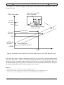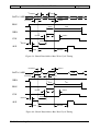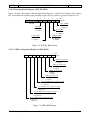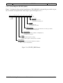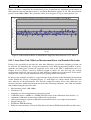
1
AS IC De si g n Ce nt er
User Manual
TDC502
Version: 2.6
Date:
2006/08/14
MSC Vertriebs GmbH
ASIC Design Center
Industriestraße 16
76297 Stutensee
Author:
Phone:
Fax:
Email:
AP
+497249/910-288
+497249/910-268
[email protected]
... competence in electronics ...
User Manual - TDC502
MSC
Page 2 of 68
Contents
1
INTRODUCTION .......................................................................................................................5
2
FEATURES .................................................................................................................................6
3
BLOCK DIAGRAM ....................................................................................................................7
4
PACKAGE AND PIN CONFIGURATION................................................................................8
4.1
4.2
5
PACKAGE ..............................................................................................................................8
PIN CONFIGURATION .............................................................................................................9
MEASURING PROCEDURE ...................................................................................................11
5.1
TIME DIFFERENCE MEASUREMENT .....................................................................................11
5.2
GENERATING CALIBRATION VALUES ..................................................................................12
5.3
MEASUREMENT RANGES AND MEASUREMENT MODES .......................................................13
5.3.1 General Measurement Cycle..........................................................................................14
5.3.2 Measurement Modes 0 and 1 .........................................................................................16
5.3.3 Measurement Modes 2 and 3 .........................................................................................17
5.3.4 Measurement Modes 4 and 5 (Burst Modes) .................................................................19
5.3.5 Measurement Modes 6 and 7 .........................................................................................20
6
FUNCTIONAL DESCRIPTION ...............................................................................................22
6.1
CALIBRATION CLOCK DIVIDER ...........................................................................................22
6.2
MEASUREMENT CHANNELS.................................................................................................23
6.2.1 Input Unit .......................................................................................................................23
6.2.2 Precounter ......................................................................................................................24
6.2.3 Retrigger Unit ................................................................................................................25
6.2.4 Auto Noise Unit .............................................................................................................25
6.2.5 Measuring Core..............................................................................................................27
6.3
HITCOUNTER .......................................................................................................................27
6.4
ARITHMETICAL LOGIC UNIT (ALU)....................................................................................28
6.5
TDC REGISTERS .................................................................................................................28
6.5.1 Read/Write Registers .....................................................................................................28
6.5.1.1 Init Register............................................................................................................28
6.5.1.2 Control Registers....................................................................................................29
6.5.1.3 Hit Register ............................................................................................................29
6.5.1.4 ALU Register .........................................................................................................29
6.5.1.5 Multiplication Registers.........................................................................................29
6.5.1.6 Interrupt Enable Register .......................................................................................29
6.5.1.7 High-Resolution Registers .....................................................................................30
6.5.1.8 Smart-Resolution Registers....................................................................................30
6.5.1.9 GPIO Configuration Register.................................................................................30
6.5.2 Read-only Registers .......................................................................................................30
6.5.2.1 Hit-Status Register .................................................................................................30
6.5.2.2 GPIO Input Register...............................................................................................30
6.5.2.3 Status Register........................................................................................................30
TDC502RefManEngV26.doc
Version: 2.6
Author: AP
MSC
User Manual - TDC502
Page 3 of 68
6.6
RAW-VALUE REGISTERS .....................................................................................................31
6.7
RESULT REGISTERS .............................................................................................................31
6.8
PROCESSOR INTERFACE.......................................................................................................31
6.8.1 General Purpose I/O-Pins...............................................................................................32
6.8.2 Data- and Control Lines .................................................................................................32
6.8.2.1 Overview................................................................................................................32
6.8.2.2 Timing Diagrams ...................................................................................................32
6.8.3 Status and Interrupt Request Flags.................................................................................36
6.8.3.1 Status Flags ............................................................................................................36
6.8.3.2 Interrupt Request Flag............................................................................................37
6.8.3.3 Correlation of Status Flags and Interrupt Request Flag set Signals.......................37
7
PROGRAMMING OF THE TDC502 .......................................................................................38
7.1
ADDRESSING .......................................................................................................................38
7.2
TDC REGISTERS .................................................................................................................39
7.2.1 Read/Write Register Formats.........................................................................................39
7.2.1.1 Init Register (INIT_REG) ......................................................................................39
7.2.1.2 Control Registers (CRTL_REG_1 / CRTL_REG_2 / CTRL_REG_3) .................40
7.2.1.3 Hit Register (HIT_REG)........................................................................................41
7.2.1.4 Interrupt Enable Register (INT_EN_REG)............................................................42
7.2.1.5 GPIO Configuration Register (GPIO_REG)..........................................................42
7.2.1.6 High-Resolution Registers (HIGH_REG_A / HIGH_REG_B).............................43
7.2.1.7 Smart-Resolution Registers (SMART_REG_A / SMART_REG_B)....................43
7.2.1.8 ALU Register (ALU_REG) ...................................................................................44
7.2.1.9 Multiplication Registers (MULT_REG_1 / MULT_REG_2 / MULT_REG_3) ...45
7.2.2 Read-only Register Formats...........................................................................................46
7.2.2.1 Hit-Status Register (HIT_STATUS_REG)............................................................46
7.2.2.2 GPIO Input Register (GPIO_IN_REG) .................................................................46
7.2.2.3 Status Register (STATUS_REG)...........................................................................47
7.3
RAW-VALUE REGISTERS .....................................................................................................48
7.3.1 Raw-Value Register Format...........................................................................................48
7.3.2 Raw-Value Data Format ................................................................................................48
7.4
RESULT REGISTERS .............................................................................................................49
7.4.1 Result Register Format...................................................................................................49
7.4.2 Result Data Formats.......................................................................................................49
8
APPENDIX................................................................................................................................50
8.1
ELECTRICAL SPECIFICATION ...............................................................................................50
8.2
RESOLUTION .......................................................................................................................51
8.2.1 How to calculate the Resolution ....................................................................................51
8.2.2 Voltage Dependence ......................................................................................................51
8.2.3 Temperature Dependence ..............................................................................................51
8.3
DIFFERENTIAL NON-LINEARITY ..........................................................................................52
8.4
MEASUREMENT RANGE I: MINIMUM/MAXIMUM MEASUREMENT PERIOD ...........................53
8.4.1 Minimum Measurement Period .....................................................................................53
8.4.2 Maximum Measurement Period.....................................................................................53
8.5
MEASUREMENT RANGE II: MINIMUM/MAXIMUM MEASUREMENT PERIOD .........................54
8.5.1 Minimum Measurement Period .....................................................................................54
8.5.2 Maximum Measurement Period.....................................................................................54
TDC502RefManEngV26.doc
Version: 2.6
Author: AP
MSC
User Manual - TDC502
Page 4 of 68
8.6
DOUBLE PULSE RESOLUTION ..............................................................................................55
8.6.1 Measurement Range I ....................................................................................................55
8.6.2 Measurement Range II ...................................................................................................55
8.7
MINIMUM PULSE WIDTH OF START- AND STOP-SIGNALS ...................................................56
8.8
SETUP AND HOLD TIME EN_STOP_A/B TO STOP_A/B....................................................56
8.9
TIMING WHEN INITIATING AND STARTING A TIME MEASUREMENT......................................57
8.10 DEAD TIMES .......................................................................................................................57
8.10.1
Dead Time at the End of a Time Measurement in Measurement Range I.................58
8.10.2
Dead Time at the End of a Time Measurement in Measurement Range II ...............59
8.10.3
Dead Time between Burst Mode Measurements .......................................................59
8.10.4
Dead Time of a Separate Calibration Measurement ..................................................60
8.10.5
Dead Time Increase due to Auto Noise and Retrigger Unit ......................................60
8.11 ALU-CALCULATION TIMES ................................................................................................61
8.12 TIMING WHEN THE FIRST RAW-VALUE OF A MEASUREMENT IS GENERATED .......................61
8.13 CURRENT CONSUMPTION ....................................................................................................62
8.14 POWER-ON CHARACTERISTICS ...........................................................................................64
8.15 MEASUREMENT RESULTS ....................................................................................................65
8.15.1
Singleshot Measurements and RMS Resolution........................................................65
8.15.2
Simultaneous Singleshot Measurements on both Channels.......................................66
8.15.3
Auto Noise Unit: Effect on Measurement Error and Standard Deviation .................67
TDC502RefManEngV26.doc
Version: 2.6
Author: AP
MSC
User Manual - TDC502
Page 5 of 68
1 Introduction
MSC Vertriebs GmbH has many years of experience in the development of high precision Time to
Digital Converters (TDCs). Our first TDC was developed in 1990 and implemented in a cost-effective Gate Array technology.
This manual describes the TDC502 - the latest member of our TDC family. The TDC502 is implemented in a 0,6µm-CMOS-process technology featuring 2.7V – 5.5V operation and is delivered in a
LQFP44 0,8 mm fine pitch package *).
Supplied with 5V the TDC502 achieves a typical resolution of up to 45ps. This resolution cannot be
achieved using conventional time measuring components. In combination with its multi-hit capability the multi-channel function of the TDC502 allows simultaneous and/or successive measurement of time differences. The Burst Measurement Mode and the integrated ALU complete the
TDC502’s performance.
The integrated measurement principle - together with the technology used - allows high-precision
time difference measurement at low power consumption. The integration of the TDC502 in batterypowered applications is a common procedure.
The TDC502 is perfectly suited for measurement of time differences. Applications like distance
measurement using laser, phase measurement, ultrasonic positioning, temperature measurement,
etc. have been implemented successfully with our TDCs many times.
Go ahead and discover the world of our TDCs.
______
*)
LQFP = Low Profile Quad Flat Package
TDC502RefManEngV26.doc
Version: 2.6
Author: AP
MSC
User Manual - TDC502
Page 6 of 68
2 Features
Channels:
2 channels with identical resolution,
consisting of a common Start- and two Stop-inputs,
programmable edge-sensitivity of the inputs,
retriggerable Start-input,
separated power supply for the Measuring Core
Resolution (5V, typ):
Half-Resolution:
Normal-Resolution:
High-Resolution:
Smart-Resolution:
Measurement ranges:
(5V, typ)
range I: short time measurement: 0ps – 10µs *)
range II: long time measurement: 180ns – 210ms *) **)
Measurement modes:
8 measurement modes with up to 10-fold multi-hit capability
and up to 10 measurements within a burst
Calibration clock:
external calibration clock required: 500 kHz - 20 MHz,
internal programmable clock divider
Calibration measurement:
automatically after time measurement or stand-alone
ALU:
calculation of every hit to start and every hit to each other hit, calibration and multiplication using a 24 bit unsigned integer number
Voltage range:
2.7 V - 5.5 V
Temperature range:
-40°C - 85°C
Processor interface:
8 bit data bus / 4 bit address bus,
programmable interrupt-pin,
4 individually programmable I/O-pins
Internal memory:
up to 10 uncalibrated measurement values
up to 2 calibrated/ multiplied measurement values
Configuration:
programmable via processor interface
Measurement improvement:
Auto Noise Unit
Package:
LQFP44 with 0.8 mm pitch
360 ps
180 ps
90 ps
45 ps
______
*)
**)
- High-Resolution: Maximum measurement period is shortened by half
- Smart-Resolution: Maximum measurement period is shortened to the fourth part
Measurement range depends on period of calibration clock
TDC502RefManEngV26.doc
Version: 2.6
Author: AP
User Manual - TDC502
MSC
Page 7 of 68
3 Block Diagram
Figure 3.1 shows the block diagram of the TDC502.
EN_STOP_A EN_STOP_B
EX_MBII
µPinterface
START
GPIO[3:0]
STOP_A
channel A
STOP_B
channel B
result
register 0
INTFLAG
ALU
CALCLK
calibration
clock
divider
TDC_READY
CLK
result
register 1
ADR[3:0]
DATA[7:0]
RDN
12 raw-value
registers
WRN
TDC registers
RSTN
CSN
ALE
Figure 3.1: TDC502 Block Diagram
The TDC offers two channels A and B for time measurement between one start at the start-input
START and up to 10 hits at the stop-inputs STOP_A and STOP_B. The uncalibrated measurement
values are stored in the raw-value registers and can either be read out via the processor interface
or processed within the ALU (Calculation of every hit to start and every hit to each other hit, calibration and multiplication using a 24 bit unsigned integer number). The ALU’s measurement results
are stored in the result registers and can be read out via the processor interface.
The configuration of the TDC as well as the selection of the measurement mode and range is done
by writing the TDC registers via the processor interface. Status information can be accessed by
reading the TDC registers.
The calibration clock, necessary for the calibration of the uncalibrated measurement values, has to
be supplied by an externally generated quartz oscillator clock at the input CALCLK. The calibration
clock is divided by the internal calibration clock divider circuit.
TDC502RefManEngV26.doc
Version: 2.6
Author: AP
User Manual - TDC502
MSC
Page 8 of 68
4 Package and Pin Configuration
4.1 Package
Figure 4.1 shows the TDC’s Plastic Quad Flat Package with 44 pins (LQFP44) and 0,8 mm pitch.
The package dimensions are specified in Table 4.1.
The TDC’s marking is ´MSC TDC502 V2´.
Figure 4.1: Package
E1 / D1
min
typ
max
A
A1
0,05
A2
1,35
1,60
0,15
1,45
10
e
b
0,30
L
0,45
α
0°
0,45
0,75
7°
0,80
D/E
Copl.
12,00
0,10
Table 4.1: Package Dimensions [mm]
TDC502RefManEngV26.doc
Version: 2.6
Author: AP
User Manual - TDC502
MSC
Page 9 of 68
4.2 Pin Configuration
Table 4.2 shows the TDC’s pin configuration. Pin names of low active signals end with ‘N’.
Pin No.
5, 7, 17,
28, 35, 39
2, 6, 12,
18, 27, 40
44
43
1
3
4
Pin name
VDD
I/O
-
Function
Power supply for internal logic and I/O’s
GND
-
Ground for internal logic and I/O’s
VDD_C
GND_C
RSTN
CALCLK
EX_MBII
In
In
Tri-state
Out, 4mA
8
9
10
11
13
14
15
16
19
20
21
22
23
24
25
26
29
30
31
32
33
GPIO0
GPIO1
GPIO2
GPIO3
DATA0
DATA1
DATA2
DATA3
DATA4
DATA5
DATA6
DATA7
ADR0
ADR1
ADR2
ADR3
ALE
RDN
WRN
CSN
TDC_READY
Bidi, 4mA
Bidi, 4mA
Bidi, 4mA
Bidi, 4mA
Bidi, 4mA
Bidi, 4mA
Bidi, 4mA
Bidi, 4mA
Bidi, 4mA
Bidi, 4mA
Bidi, 4mA
Bidi, 4mA
In
In
In
In
In
In
In
In
Out, 4mA
34
INTFLAG
Out, 4mA
36
START
In
Power supply for measuring core
Ground for measuring core
Power-on reset (low active)
Input for calibration clock: 500 kHz - 20 MHz
- Expansion of measurement range II enabled:
EX_MBII toggles at every overflow of the precounter: 0-1-0-...
- Expansion of measurement range II disabled:
high impedance
Bit0 general purpose I/O, default: high impedance
Bit1 general purpose I/O, default: high impedance
Bit2 general purpose I/O, default: high impedance
Bit3 general purpose I/O, default: high impedance
Bit0 data bus
Bit1 data bus
Bit2 data bus
Bit3 data bus
Bit4 data bus
Bit5 data bus
Bit6 data bus
Bit7 data bus
Bit0 address bus
Bit1 address bus
Bit2 address bus
Bit3 address bus
Address latch enable (high active)
Read strobe (low active)
Write strobe (low active)
Chip select (low active)
0 : TDC not ready, measurement channels disabled
1 : TDC ready for measurement, TDC waits for start
0 : no interrupt request
1 : interrupt request
Common start-input
TDC502RefManEngV26.doc
Version: 2.6
Author: AP
User Manual - TDC502
MSC
Pin No.
37
Pin name
EN_STOP_B
I/O
In
38
41
42
STOP_B
STOP_A
EN_STOP_A
In
In
In
*)
Page 10 of 68
Function
Enable stop-input channel B *):
0 : Stop-input STOP_B disabled, cannot be enabled
via software.
1 : Stop-input STOP_B enabled, if not disabled
via software.
Stop-input channel B
Stop-input channel A
Enable stop-input channel A *):
0 : Stop-input STOP_A disabled, cannot be enabled
via software.
1 : Stop-input STOP_A enabled, if not disabled
via software.
In measurement range II the stop-input of the selected channel has to be enabled during the
whole time measurement.
Remarks:
•
•
•
•
All inputs are CMOS.
Connect all unused inputs to GND.
Data bus DATA[7:0] is not allowed to float: please pull up or down (with e.g. 10kΩ).
Do not connect unused outputs.
Table 4.2: Pin Function List
TDC502RefManEngV26.doc
Version: 2.6
Author: AP
User Manual - TDC502
MSC
Page 11 of 68
5 Measuring Procedure
The TDC502 provides two identical measurement channels A and B with a common start-input and
two independent stop-inputs. The resolution of both channels is identical. Via the processor interface a resolution of 45ps (Smart Resolution), 90ps (High Resolution), 180ps (Normal Resolution) or 360ps (Half Resolution) is selectable (5V, typ.).
5.1 Time Difference Measurement
As shown in Figure 5.1, one edge-sensitive start-input and two edge-sensitive stop-inputs are available for measuring the time differences tRESi. The stop-inputs represent the measurement channels
A and B. A start on the start-input starts the time measurement in the measuring core. Depending on
the selected measurement mode every stop on the stop-inputs is detected as a so called hit and the
time “hit – start” is measured and stored as measurement value VAL in one of the raw-value registers. The time measurement ends, when the last hit – up to 10 hits are configurable – is detected.
With the measurement values of the raw-value registers all possible time differences tRESi (hit to
start, hit to another hit) can be calculated, either externally or using the internal ALU. The ALU’s
measurement results (positive and negative time differences are possible!) are stored in the result
registers.
TDC502
raw-value
registers
START
STOP_A
measuring
core
VAL
STOP_B
tRES1
tRES6
tRES2
RES
tRES3
tRES4
ALU
tRES5
start
result
registers
CALCLK
1. hit
1. hit
2. hit
channel A channel B channel A
Figure 5.1: Time Difference Measurement Example
The measurement value VAL is dependant on the temperature and the supply voltage. Therefore it
has to be weighted according to the TDC characteristic (see Figure 5.2). Offset and gradient of the
characteristic have to be determined by a so-called calibration measurement.
TDC502RefManEngV26.doc
Version: 2.6
Author: AP
User Manual - TDC502
MSC
Page 12 of 68
TDC raw-value
measurement value
calibration value
CAL
VAL
OFFSET
t
tRES
tCAL
Figure 5.2: Characteristic of the TDC Measuring Core
5.2 Generating Calibration Values
To generate the calibration values OFFSET and CAL, shown in Figure 5.2, a calibration clock has
to be provided at the TDC’s pin CALCLK. This clock is the absolute time reference and therefore it
must have the precision of a quartz crystal. The calibration clock is divided by the internal calibration clock divider. The resulting clock CLK is the internal reference clock. Its period length is measured during a calibration measurement using the measuring core.
CAL
CLK
tCAL
Figure 5.3: Calibration Measurement
Depending on the measurement mode the calibration measurement is performed for only one channel or both. Just like a measurement value VAL the resulting calibration values CAL A / CAL B
and OFFSET A / OFFSET B are stored in the raw-value registers. The time tCAL is well known: It
is the divided calibration clock period.
A calibration measurement is performed either automatically after a timing measurement or has to
be started separately from time to time depending on the measurement mode.
Unlike the measurement and calibration values VAL and CAL, the offset is very constant within a
wide range of temperature and supply voltage. So it’s not necessary to generate OFFSET all the
times a calibration measurement is performed. Via software it’s possible to disable the offsetgeneration during calibration measurement, resulting in a higher precision accuracy, when adapted
to the measurement application properly.
TDC502RefManEngV26.doc
Version: 2.6
Author: AP
User Manual - TDC502
MSC
Page 13 of 68
5.3 Measurement Ranges and Measurement Modes
The TDC502 offers two measurement ranges:
• Range I: use of TDC-core for short time measurement: 0ps - 10µs *)
• Range II: use of TDC-core and precounter for long time measurement: 180ns – 210ms *) **)
The TDC502 provides eight measurement modes, programmable via the processor interface. In
Table 5.1 all measurement modes are listed.
Measurement
Automode
calibration
0
yes
•
•
1
no
•
•
2
yes
•
•
•
3
no
•
4
yes
•
•
5
no
•
6
yes
•
•
•
•
7
no
•
Short description
Measurement range I
1 channel (A or B programmable) with 10-fold multi-hit
capability
Double pulse resolution: 25ns (5V, 25°C)
ALU: Calculation of every hit to start and every hit to each other
hit, negative results possible
Measurement range I
2 channels with common start and 4-fold multi-hit capability each
Double pulse resolution: 0ps (different channels) resp. 25ns (same
channel; 5V, 25°C)
ALU: Calculation of every hit to start and every hit to each other
hit, negative results possible
Measurement range I
1 channel (A or B programmable) with 10-fold burst capability
‘start-stop’
Dead time between burst mode measurements ‘start-stop’: 100ns
(5V, 25°C)
ALU: calculation of each ‘start-stop’
Measurement range II
1 channel (A or B programmable) with 4-fold multi-hit capability
Double pulse resolution: 1,5 * (divided) period of calibration clock
+ 105ns (5V, 25°C)
ALU: Calculation of every hit to start and every hit to each other
hit, negative results not possible
Note:
• In measurement modes 1, 3, 5 and 7 separate calibration measurements have to be performed on occasion by
activating the action-bit ‘separate calibration measurement’ within the Init Register (see Chapter 6.5.1.1).
Table 5.1: Measurement Modes
_________
*)
- typical at 5V, 25°C
- High-Resolution: Maximum measurement period is shortened by half
- Smart-Resolution: Maximum measurement period is shortened to the fourth part
**) Measurement range depends on period of calibration clock
TDC502RefManEngV26.doc
Version: 2.6
Author: AP
User Manual - TDC502
MSC
Page 14 of 68
5.3.1 General Measurement Cycle
Figure 5.4 shows the flowchart of a general measurement cycle. At the very beginning of a measurement cycle the measurement mode, the usage of the ALU and so on has to be specified within
the TDC’s Control Registers. In the Hit Register the number of hits or burst mode measurements
has to be defined a measurement cycle consists of. For optimization the TDC’s differential nonlinearity the Smart- and High-Resolution Registers have to be configured. If the ALU is used for
calculation the measurement results, the ALU Register and maybe the Multiplication Registers have
to be configured as well. For detailed information on the TDC registers refer to Chapter 6.5.
The actual measurement cycle is initiated by activating the action-bit ‘time measurement’ within the
Init-Register: Now the TDC is ready for measurement and waits for a start-signal on the start-input
START. After start has taken place the time measurement continues until the number of hits on the
Stop-inputs STOP_A and STOP_B or the number of burst mode measurements specified in the Hit
Register (cp. Chapter 6.5.1.3) is reached. If the ALU is not used for calculations the action-bit ‘time
measurement’ is cleared automatically now in the measurement modes 1, 3, 5 and 7.
In measurement mode 2 an automatic calibration measurement follows, performed on both channels, in measurement modes 0, 4 and 6 on the channel selected in the Control Register. When the
calibration measurement is completed and the ALU is not used for calculations the action-bit ‘time
measurement’ is cleared now.
Starting point
*) Configuration of Control-, Hit-, High- and
Smart-Resolution Registers
*) Configuration of ALU- and Multiplication
Registers
Activation of action-bit “time measurement“
within the Init Register
*)
Time measurement
**) Calibration measurement
New configuration of Control-,
ALU- and Multiplication Registers
Activation of the action-bit “ALU calculation“ within the Init Register
ALU calculation
*) Configuration allowed only when no action-bit is set within the Init Register
**) Possibility of separate calibration measurements via direct command
Figure 5.4: General Measurement Cycle Flow
TDC502RefManEngV26.doc
Version: 2.6
Author: AP
MSC
User Manual - TDC502
Page 15 of 68
If the ALU is used, now the first calculation according to the ALU-calculation rules and specifications within the Control-, ALU- and Multiplication Registers is executed and the result of this first
calculation within a measurement cycle is always stored in result register 0. Afterwards the actionbit ‘time measurement’ is cleared automatically.
After modifying the ALU-calculation rules, repetitive activation of the action-bit ‘ALU calculation’
within the Init Register makes an unlimited number of calculations possible. The results are stored
then alternately in the result registers 1, 0, 1, ... . After completion a calculation the action-bit ‘ALU
calculation’ is cleared automatically each time.
For another time measurement the action-bit ‘time measurement’ has to be reactivated. The first
ALU-calculation result for a new measurement is always stored in result register 0.
Please notice, that configuring the Control-, Hit-, ALU-, Multiplication-, Smart- and High-Resolution Registers is only allowed when no action-bit is set within the Init Register.
TDC502RefManEngV26.doc
Version: 2.6
Author: AP
User Manual - TDC502
MSC
Page 16 of 68
5.3.2 Measurement Modes 0 and 1
Mode’s 0 and 1 measurements are executed within measurement range I using the measuring core.
As shown in Figure 5.5, one channel with up to 10 hits and a double pulse resolution of 25ns (5V,
25°C) is available. Via software channel A or channel B is selectable. When the time measurement
is completed in measurement mode 0 an automatic calibration measurement on the selected channel
follows according to Chapter 5.2.
time measurement
> 25 ns
START
STOP_A
STOP_A resp. STOP_B
start
hit 1
hit 2
hit 10
VAL1
VAL2
VAL10
Figure 5.5: Measurement Modes 0 and 1
The time difference tRES between hit x (1 ≤ x ≤ 10) and start is calculated using the divided calibration clock period tCAL, the calibration values CAL and OFFSET and the measurement value VALx
in accordance with the TDC’s quantisation characteristic shown in Figure 5.2 as follows:
(1)
tRES =
VALx - OFFSET
_______________
* tCAL
CAL - OFFSET
The time difference tRES between hit y (1 ≤ y ≤ 10) and hit x (1 ≤ x ≤ 10) is calculated using the divided calibration clock period tCAL and the raw-values VALy, VALx, CAL and OFFSET in accordance with the TDC’s quantisation characteristic shown in Figure 5.2 as follows:
(2)
tRES =
VALy - VALx
______________
* tCAL
CAL - OFFSET
If the ALU is used for calculation the time difference tRES, the fraction of formulas 1 and 2 is computed during calibration. If the ALU is used not only for calibration but also for multiplication, tCAL
has to be set up within the multiplication registers to numbers between 0 and 2. If the multiplication
is disabled via software, tCAL remains 1 and no multiplication is executed.
If VALx is greater than VALy within formula 2, the measurement result tRES becomes negative
when using the TDC’s ALU.
TDC502RefManEngV26.doc
Version: 2.6
Author: AP
User Manual - TDC502
MSC
Page 17 of 68
5.3.3 Measurement Modes 2 and 3
Mode’s 2 and 3 measurements are executed within measurement range I using the measuring core.
As shown in Figure 5.6, both channels with a common start and up to 4 hits each are available. The
double pulse resolution is 25ns (5V, 25°C) for hits on the same channel and 0ns for hits on different
channels. When the time measurement is completed in measurement mode 2 an automatic calibration measurement on both channels follows according to Chapter 5.2.
time measurement
> 25 ns
0 ps
START
STOP_A
STOP_B
common start
hit 1 ch. A
hit 1 ch. B
hit 2 ch. B
hit 2 ch. A
hit 4 ch. B
hit 4 ch. A
VAL1 A
VAL1 B
VAL2 B
VAL2 A
VAL4 B
VAL4 A
Figure 5.6: Measurement Modes 2 and 3
The time difference tRES between hit x (1 ≤ x ≤ 4) on channel A (resp. channel B) and common start
is calculated using the divided calibration clock period tCAL and the raw-values VALx A, CAL A
and OFFSET A (resp. VALx B, CAL B and OFFSET B) in accordance with the TDC’s quantisation characteristic shown in Figure 5.2 as follows:
(3)
tRES =
VALx A – OFFSET A
___________________
* tCAL
CAL A – OFFSET A
resp.
(4)
tRES =
VALx B – OFFSET B
___________________
* tCAL
CAL B – OFFSET B
The time difference tRES between hit y (1 ≤ y ≤ 4) and hit x (1 ≤ x ≤ 4) on the same channel is calculated using the divided calibration clock period tCAL and the raw-values VALy A, VALx A, CAL
A and OFFSET A for channel A (VALy B, VALx B, CAL B and OFFSET B for channel B) in
accordance with the TDC’s quantisation characteristic shown in Figure 5.2 as follows:
TDC502RefManEngV26.doc
Version: 2.6
Author: AP
User Manual - TDC502
MSC
(5)
tRES =
Page 18 of 68
VALy A – VALx A
___________________
* tCAL
CAL A – OFFSET A
resp.
(6)
tRES =
VALy B – VALx B
___________________
* tCAL
CAL B – OFFSET B
The time difference tRES between hit y (1 ≤ y ≤ 4) on channel B and hit x (1 ≤ x ≤ 4) on channel A is
calculated using the divided calibration clock period tCAL and the raw-values VALy B, VALx A,
CAL B, OFFSET B and OFFSET A in accordance with the TDC’s quantisation characteristic
shown in Figure 5.2 as follows:
(7)
tRES =
__________________________________________
(VALy B – OFFSET B) – (VALx A – OFFSET A)
* tCAL
CAL B – OFFSET B
The time difference tRES between hit y (1 ≤ y ≤ 4) on channel A and hit x (1 ≤ x ≤ 4) on channel B is
calculated using the divided calibration clock period tCAL and the raw-values VALy A, VALx B,
CAL A, OFFSET A and OFFSET B in accordance with the TDC’s quantisation characteristic
shown in Figure 5.2 as follows:
(8)
tRES =
__________________________________________
(VALy A – OFFSET A) – (VALx B – OFFSET B)
* tCAL
CAL A – OFFSET A
If the ALU is used for calculation the time difference tRES, the fraction of the formulas 3 to 8 is
computed during calibration. If the ALU is used not only for calibration but also for multiplication,
tCAL has to be set up within the multiplication registers to numbers between 0 and 2. If the multiplication is disabled via software, tCAL remains 1 and no multiplication is executed.
When using the TDC’s ALU the measurement result tRES may become negative.
Application Note:
When the stop-inputs STOP_A and STOP_B are combined the same time difference can be measured simultaneously on both channels. Averaging the two measurement results will improve the
measurement’s accuracy and double the TDC’s resolution of up to 23ps at 5V resp. 33ps at 3.3V
(typ).
TDC502RefManEngV26.doc
Version: 2.6
Author: AP
User Manual - TDC502
MSC
Page 19 of 68
5.3.4 Measurement Modes 4 and 5 (Burst Modes)
Mode’s 4 and 5 measurements are executed within measurement range I using the measuring core.
As shown in Figure 5.7, one channel with up to 10 burst mode measurements ‘start-stop’ is available. Via software channel A or channel B is selectable. For each burst mode measurement the
whole measurement range (0ps – 10µs *)) is usable. The dead time between burst mode measurements is 100ns (5V, 25°C, see Appendix 8.10.3). When the last burst mode measurement is completed in measurement mode 4 an automatic calibration measurement on the selected channel follows according to Chapter 5.2.
burst mode measurements
> 100ns
START
STOP_A
STOP_A resp. STOP_B
VAL1
VAL2
measurement 1
measurement 2
VAL10
measurement 10
Figure 5.7: Burst Modes 4 and 5
The time difference tRES of burst mode measurement x (1 ≤ x ≤ 10) is calculated using the divided
calibration clock period tCAL, the calibration values CAL and OFFSET and the measurement value
VALx in accordance with the TDC’s quantisation characteristic shown in Figure 5.2 as follows:
(9)
tRES =
VALx - OFFSET
_______________
* tCAL
CAL - OFFSET
If the ALU is used for calculation the time difference tRES, the fraction of formula 9 is computed
during calibration. If the ALU is used not only for calibration but also for multiplication, tCAL has to
be set up within the multiplication registers to numbers between 0 and 2. If the multiplication is
disabled via software, tCAL remains 1 and no multiplication is executed.
When using the TDC’s ALU the measurement result tRES may become negative.
______
*)
- typical at 5V, 25°C
- High-Resolution: Maximum measurement period is shortened by half
- Smart-Resolution: Maximum measurement period is shortened to the fourth part
TDC502RefManEngV26.doc
Version: 2.6
Author: AP
User Manual - TDC502
MSC
Page 20 of 68
5.3.5 Measurement Modes 6 and 7
Mode’s 6 and 7 measurements are executed within measurement range II using both, the measuring
core and the precounter. As shown in Figure 5.8, one channel with up to 4 hits and a double pulse
resolution of 1,5 * tCAL + 105ns (5V, 25°C) is available. In this formula tCAL is the divided calibration clock period. Via software channel A or channel B is selectable. The minimum measurement
period is 1,5 * tCAL +105ns (5V, 25°C), too. When the time measurement is completed in measurement mode 6 an automatic calibration measurement on the selected channel follows according to
Chapter 5.2.
As shown in Figure 5.8 for each hit time measurements are divided into three stages:
1. stage,
for all
hits in
common
2. stage,
separated for
each hit
VAL0
3. stage
for
hit 1
3. stage
for
hit 2
VAL1
VAL2
3. stage
for
hit 4
---
VAL4
CLK
START
precounter
0
0
1
precounter
----
0
0
1
0
0
1
precounter
----
PRE1 - 1
PRE1
---
PRE2
----
PRE4
STOP_A resp.
STOP_B
start
hit 1
≥ 1.5 * tCAL + 105ns
≥ 1.5 * tCAL + 105ns
*)
hit 2
hit 4
*)
Figure 5.8: Measurement Modes 6 and 7
In the first stage of the measurement the measuring core determines the time difference between
the start-signal and the following rising edge of the divided calibration clock for all hits in common.
The output is stored as measurement value VAL0 in a raw-value register. In the second stage of the
measurement the precounter counts the clock periods tCAL of the divided calibration clock CLK
between the start-signal and each hit. The results are stored as precounter values PREx (1 ≤ x ≤ 4)
in the raw-value registers. In the thirdstaget of the measurement the time between each hit and the
following rising edge of the divided calibration clock is measured using the measuring core once
again. The results are stored as measurement values VALx (1 ≤ x ≤ 4) in the raw-value registers.
TDC502RefManEngV26.doc
Version: 2.6
Author: AP
User Manual - TDC502
MSC
Page 21 of 68
The time difference tRES between hit x (1 ≤ x ≤ 4) and start is calculated using the divided calibration clock period tCAL and the raw-values VAL0, VALx, PREx, CAL and OFFSET in accordance
with the TDC’s quantisation characteristic shown in Figure 5.2 as follows:
(10) tRES =
VAL0 - VALx
______________
+ PREx
CAL - OFFSET
* tCAL
The time difference tRES between hit y and hit x (1 ≤ x ≤ 3, 2 ≤ y ≤ 4, x < y) is calculated using the
divided calibration clock period tCAL and the raw-values VALx, PREx, VALy, PREy, CAL and
OFFSET in accordance with the TDC’s quantisation characteristic shown in Figure 5.2 as follows:
(11) tRES =
VALx - VALy
______________
+ PREy - PREx
CAL - OFFSET
* tCAL
If the ALU is used for calculation the time difference tRES, the bracket term of formulas 10 and 11
is computed during calibration. If the ALU is used not only for calibration but also for multiplication, tCAL has to be set up within the multiplication registers to numbers between 0 and 2. If the
multiplication is disabled via software, tCAL remains 1 and no multiplication is executed.
In measurement range II the TDC’s ALU computes positive results only.
TDC502RefManEngV26.doc
Version: 2.6
Author: AP
User Manual - TDC502
MSC
Page 22 of 68
6 Functional Description
6.1 Calibration Clock Divider
Figure 6.1 shows the principle function of the calibration clock divider.
1:1
1:2
CALCLK
divider
CLK
1:4
1:128
Figure 6.1: Calibration Clock Divider
The external calibration clock CALCLK is divided by the calibration clock divider. The division
factors are programmable and can be set to 1, 2, 4, 8, 16, 32, 64 or 128.
Since a calibration measurement is always done by the TDC’s measuring core, it is necessary to
ensure that in measurement range I the clock period tCAL of the divided calibration clock CLK is not
larger than 10µs*) (5V, typ). Otherwise the measuement of the calibration clock period would cause
a measuring core overflow OV_CORE (cp. formula A1 in Appendix 8.4.2). In measurement range
II the divided calibration clock period tCAL shouldn’t be larger than 6.6µs**) (5V, typ) (cp. formula
A4 in Appendix 8.5.2).
Depending on the power supply VDD the maximum frequency of the divided calibration clock
CLK is limited as follows:
•
•
•
4.5V ≤ VDD ≤ 5.5 V: 20 MHz
3.0V ≤ VDD < 4.5 V: 10 MHz
2.7V ≤ VDD < 3.0 V: 6 MHz
In order to achieve high precision accuracy when measuring in measurement range I, the division
factor should be selected in such a way, that the (largest) time difference to be measured is in the
range of half the calibration clock period length. To achiev best measurement results in measurement range II the period of the divided calibration clock should be as long as possible.
______
*)
**)
High-Resolution: 5µs, Smart-Resolution: 2.5µs
High-Resolution: 3.3µs, Smart-Resolution: 1.6µs
TDC502RefManEngV26.doc
Version: 2.6
Author: AP
User Manual - TDC502
MSC
Page 23 of 68
6.2 Measurement Channels
Figure 6.2 shows the block diagram of the measurement channels.
Enable TDC
Polarity Start
Enable Stop_A Polarity Stop_A
Enable Stop_B Polarity Stop_B
input unit
Retrigger
Enable
START
Start
retrigger
unit
Auto Noise
Enable
STOP_A
measuring
core
Stop_A
auto noise
unit
STOP_B
Stop_B
CLK
precounter
OV_PRE / EX_MBII
PRE
VAL, OFFSET, CAL
OV_CORE
Figure 6.2: Measurement Channels Block Diagram
6.2.1 Input Unit
The input unit handles the incoming start-, stop- and calibration clock-signals using the following
control signals:
• Enable TDC:
The measurement channels are enabled by activating the action-bit ‘time measurement‘ within
the Init Register. If the channels are disabled, no start-, stop- and calibration clock-signals will
reach the measuring core and no measurement will take place. As an exception calibration
measurements take place, no matter if the measurement channels are enabled or not.
TDC502RefManEngV26.doc
Version: 2.6
Author: AP
MSC
User Manual - TDC502
Page 24 of 68
• Enable Stop_A / Enable Stop_B:
Using the pins EN_STOP_A and EN_STOP_B the stop-inputs STOP_A and STOP_B of the
measurement channels can be disabled. No stop-signals will be passed to the measuring core. If
the stop-inputs are enabled by EN_STOP_A or EN_STOP_B, they can also be enabled/disabled
by software. Please notice, that in measurement range II the stop-input of the selected channel
has to be enabled during the whole time measurement.
• Polarity Start / Polarity Stop_A / Polarity Stop_B:
The edge-sensitivities of the TDC’s start- and stop-inputs START, STOP_A and STOP_B are
adjusted independently from each other by software. The input unit therefore triggers on rising or
falling edges of the start- and stop-signals depending on the configuration.
Furthermore the input unit decides, which signal (start, stop or calibration clock) has to be passed
on as a start- or stop-signal to the measuring core, depending on the measurement mode and on the
partial step of the measurement cycle.
6.2.2 Precounter
In measurement range II the precounter counts the clock periods tCAL of the divided calibration
clock CLK between the start-signal and up to four hits. The precounter is enabled by the start-signal
and disabled by the last hit, defined in the hit register (cp. Chapter 6.5.1.3). With every hit the
current 15-bit counter reading PRE is stored as precounter value in a raw-value register. In doing so
the maximum measurement period of measurement range II is tMBIImax = 215 * tCAL (cp. Appendix
8.5.2).
If the time difference the precounter has to measure exceeds the maximum measurement period, a
precounter overflow OV_PRE will occur and - if enabled - the signal I_OV_PRE sets the TDC’s
interrupt request flag INTFAG (cp. Chapter 6.8.3.1). Thus, the ongoing measurement cycle is
aborted including any automatic calibration measurement and ALU-calculations. All data (measurement and precounter values) already stored in the raw-value registers will remain unaffected.
Even if the expansion of measurement range II is enabled via software, a precounter overflow
OV_PRE will occur and - if enabled - the signal I_OV_PRE will set the TDC’s interrupt request
flag INTFAG as well. The ongoing measurement cycle, however, is not aborted and the TDC’s signal EX_MBII toggles at every overflow of the precounter: 1st overflow: 0 -> 1, 2nd overflow: 1 -> 0,
3rd overflow: 0->1 etc.
Remarks:
• If the expansion is disabled, EX_MBII remains on high impedance.
• EX_MBII is only cleared on power-on and soft reset or by activating the action-bit ‘time measurement’, whereas it
is not cleared by activating the action-bit ‘separate calibration measurement‘, for example.
• If the expansion is enabled, ALU-calculations are only valid before 1st overflow.
TDC502RefManEngV26.doc
Version: 2.6
Author: AP
User Manual - TDC502
MSC
Page 25 of 68
6.2.3 Retrigger Unit
If the retrigger unit is enabled, the measurement is re-started at the appearance of every start at the
TDC’s start-input START, as long as no stop (resp. hit) has been detected.
As shown in Figure 6.3, the determined time difference tRES is the time between the last start and
the stop/hit. If the retrigger unit isn't enabled then the time difference between the first start and the
stop/hit is measured. The retrigger unit can be enabled by software for the measurement modes 0 to
5 (measurement range I).
START
e.g. STOP_A
tRES with Retrigger Unit
tRES without Retrigger Unit
Figure 6.3 Measurement with and without Retrigger Unit
Remarks:
• The maximum measurement period in measurement range I is 10µs (resp. 5 µs (High-Resolution), 2,5µs (Smart
Resolution), (25°C, 5V), see Appendix 8.4.2), no matter if the retrigger unit is enabled or not. So if the time difference between a retriggering start and the start before exceeds the maximum measurement period, a measuring core
overflow OV_CORE will occur and - if enabled - the signal I_OV_CORE sets the TDC’s interrupt request flag
INTFLAG (cp. Chapter 6.8.3). Thus, the ongoing measurement cycle is aborted including any automatic calibration
measurement and ALU-calculations and the retriggering start will not restart the measurement.
• After the first start the minimum measurement period is 0,8 * ts. The time ts is the minimum pulse width of start- and
stop-signals (cp. Appendix 8.7). After any retriggering start the minimum measurement period is 0ps as usual.
6.2.4 Auto Noise Unit
The characteristic of the TDC is a straight line with offset and upward gradient, which due to the
digital measurement procedure possesses quantisation stages – so called LSBs (Least Significant
Bits) - with the width of the resolution. For a single measurement one therefore gets a quantisation
error of up to one quantisation stage at ideal quantisation. This precision is sufficient for most applications.
A higher precision can be achieved when the measurement of the same time is repeated several
times and statistical methods are used:
Changing the existing offset of the characteristic for each single measurement by delaying the stopsignal according to Figure 6.4 causes sampling at different positions of the characteristic, especially
when measuring very constant time differences of a low noise signal. If the same offset shift is still
present during the generation of the calibration values for the associated measurement value, the
total offset is eliminated during the time difference calculation according to the formulas 1 to 11
TDC502RefManEngV26.doc
Version: 2.6
Author: AP
User Manual - TDC502
MSC
Page 26 of 68
(see Chapter 5.3). When averaging all the single measurements, there quantisation errors are
averaged as well.
quantisation stage (LSB):
width = resolution
TDC raw-value
CAL with
auto noise
CAL
different offsets, generated
by auto noise unit
VAL with
auto noise
time difference
to be measured
VAL
OFFSET with
auto noise
OFFSET
offset enlargement
by delaying the stop signal
t
tRES
Figure 6.4: Influence of the Auto Noise Unit on the Characteristics of the TDC Measuring Core
If the auto noise unit is enabled a channel-specific delay is generated by a pseudo-random number
generator. This delay is added to the already existing offset of the respective channel and can be
changed with every activation of the action-bit ‘clock auto noise‘ within the Init Register. The pseudo-random number generator provides 32 different states each generating another delay. The pseudo-random number generator is cleared on power-on reset only.
Remarks:
• Maximum auto noise delay: 11ns (5V, typ, see Appendix 8.10.5).
• The auto noise unit is available only in the measurement modes 0 to 5 (measurement range I).
• For accuracy reasons averaging over 32, 64, 96, etc. measurements is recommended.
TDC502RefManEngV26.doc
Version: 2.6
Author: AP
MSC
User Manual - TDC502
Page 27 of 68
6.2.5 Measuring Core
The measuring core determines the time difference between the start-signal and the hits with a programmable resolution of 45ps (Smart-Resolution), 90ps (High-Resolution), 180ps (Normal-Resolution) or 360ps (Half-Resolution) (25°C, 5V). The measuring core stores the measurement- and calibration values in the raw-value registers for further processing.
If the time difference the core has to measure exceeds the maximum measurement period (cp.
Chapter 8.4.2), a measuring core overflow OV_CORE will occur and - if enabled - the signal
I_OV_CORE sets the TDC’s interrupt request flag INTFAG (cp. Chapter 6.8.3.1). Thus, the ongoing measurement cycle is aborted including any automatic calibration measurement and ALUcalculations.
To achieve a high precision accuracy electrical coupling effects can be minimized applying the
TDC’s separated power supply pins for the measuring core.
6.3 Hitcounter
Two hitcounters are provided, one for each channel.
Depending on the measurement mode and the channel selector bit within the Control Register
CTRL_REG_1 the hitcounters register the hits detected on the respective channel. If the number of
hits (resp. burst mode measurements) defined in the Hit Register (cp. Chapter 6.5.1.3) is reached,
the time measurement is completed and an automatic calibration measurement or ALU-calibration
may follow.
The Hit-Status Register HIT_STATUS_REG (cp. Chapter 6.5.2.1), readable via the processor interface, reflects the current state of the hitcounters.
Remarks:
• The hitcounters are cleared on power-on and soft reset or by activating the action-bits ‘time measurement’ or
’separate calibration measurement’.
• The hitcounters are disabled during any kind of calibration measurements.
TDC502RefManEngV26.doc
Version: 2.6
Author: AP
MSC
User Manual - TDC502
Page 28 of 68
6.4 Arithmetical Logic Unit (ALU)
The ALU executes time difference calculations (hit to start / hit to another hit, calibration and multiplication using a 24 bit unsigned integer number, negative results are possible!) on the measurement-, calibration- and precounter values of the raw-value registers in accordance with the formulas
1 to 11 (see Chapter 5.3).
For doing calculations the ALU requires calculation rules defined via software in the Control-,
ALU- and Multiplication Registers.
If the ALU is enabled via software, the first ALU-calculation within a measurement cycle starts
automatically following a time- or calibration measurement. The result of the first ALU-calculation
within a measurement cycle is always stored in result register 0. After modifying the calculation
rules an unlimited number of calculations can be initiated by activating the action-bit ‘ALU calculation’ again and again. The results are stored then alternating in the result registers 1, 0, 1, 0, .. .
During ALU-calculations the status flag ALU_BUSYN is active (low). When the result is calculated and stored in one of the two result registers, the status signal ALU_BUSYN is cleared (reset to
‘1’) and - if enabled - the signal I_ALU_END sets the TDC’s interrupt request flag INTFAG (cp.
Chapter 6.8.3.1).
The ALU is provided with its own clock generator and is independent from TDC-external clocks. A
calibration takes approx. 1,2µs (25°C, 5V) and the following multiplication approx. 2µs (25°C, 5V).
Please see Appendix 8.11 for exact ALU-calculation times (calibration / multiplication).
6.5 TDC Registers
The width of all TDC registers is 8 bit. They are accessible via the processor interface (see Chapter
6.8). For addressing the registers refer to Chapter 7.1.
6.5.1 Read/Write Registers
All read/write registers are written with the rising edge of the signal WRN.
Please notice that it’s only allowed to write the Control-, Hit-, Highresolution-, Smartresolution-,
ALU- and Multiplication Registers when no action-bit is set within the Init Register (cp. Chapter
5.3.1).
6.5.1.1 Init Register
The Init Register provides direct commands which are executed by setting the register’s bits to ‘1’
(= activation of the action-bits). In doing so a time measurement, a separate calibration measurement or a ALU calculation is started or a soft reset is executed. For detailed information on the individual register bits refer to Chapter 7.2.1.1, Init Register (INIT_REG).
TDC502RefManEngV26.doc
Version: 2.6
Author: AP
User Manual - TDC502
MSC
Page 29 of 68
6.5.1.2 Control Registers
There are three Control Registers all in all. Here the measurement mode, the division factor for the
calibration clock divider as well as the edges of the start- and stop-signals, on which the TDC will
trigger, are selected. A detailed description of the individual register bits is given in Chapter 7.2.1.2,
Control Registers (CRTL_REG_1 / CRTL_REG_2 / CTRL_REG_3).
6.5.1.3 Hit Register
In the Hit Register the number of hits for both channels is defined a measurement cycle consists of.
In the burst mode the number of burst mode measurements ‘start – stop’ is defined. For detailed
information on the individual register bits refer to Chapter 7.2.1.3, Hit Register (HIT_REG).
6.5.1.4 ALU Register
In this register the ALU-calculation rules are defined, according to the formulas 1 to 11 (see Chapter 5.3).
ALU-calculation rule format:
Calculate the time difference between the event of the register’s HIGH_NIBBLE (hit, burst mode
measurement) and the event of the register’s LOW_NIBBLE (hit, start, common start).
In short:
HIGH_NIBBLE – LOW_NIBBLE
For detailed information on the individual register bits refer to Chapter 7.2.1.8, ALU Register
(ALU_REG).
6.5.1.5 Multiplication Registers
In these three registers a 24 bit unsigned integer number (value range: 0 to 2) is specified. If the
multiplication is enabled via software the ALU uses this value for multiplication according to the
formulas 1 to 11 (see Chapter 5.3). For detailed information on the individual register bits refer to
Chapter 7.2.1.9, Multiplication Registers (MULT_REG_1 / MULT_REG_2 / MULT_REG_3).
6.5.1.6 Interrupt Enable Register
In this register up to six IRQ flag set signals can be enabled for interrupt generation on pin INTFLAG. For detailed information on the individual register bits refer to Chapter 7.2.1.4, Interrupt
Enable Register (INT_EN_REG).
TDC502RefManEngV26.doc
Version: 2.6
Author: AP
MSC
User Manual - TDC502
Page 30 of 68
6.5.1.7 High-Resolution Registers
There is a High-Resolution Register for each channel. In order to achieve an minimized differential
non-linearity fine-tuning for High- and Smart-Resolution is done in these registers. For detailed
information on the individual register bits refer to Chapter 7.2.1.6, High-Resolution Registers
(HIGH_REG_A / HIGH_REG_B).
6.5.1.8 Smart-Resolution Registers
There is a Smart-Resolution Register for each channel. In order to achieve an minimized differential
non-linearity fine-tuning for Smart-Resolution is done in these registers. A detailed description of
the individual register bits is given in Chapter 7.2.1.7, Smart-Resolution Registers
(SMART_REG_A / SMART_REG_B).
6.5.1.9 GPIO Configuration Register
The TDC provides four general purpose I/O-pins GPIO0, GPIO1, GPIO2 and GPIO3, individually
configurable as input or output via this register. A pin configured as output drives a ‘0’ or ‘1’, according to the level specified also in this register. A detailed description of the individual register
bits is given in Chapter 7.2.1.5, GPIO Configuration Register (GPIO_REG).
6.5.2 Read-only Registers
6.5.2.1 Hit-Status Register
The Hit-Status Register reflects the current number of hits or burst mode measurements detected for
each channel. A detailed description of the individual register bits is given in Chapter 7.2.2.1, HitStatus Register (HIT_STATUS_REG).
6.5.2.2 GPIO Input Register
The levels of all four general purpose I/O-pins GPIO0, GPIO1, GPIO2 and GPIO3 can be read via
the GPIO Input Register. A detailed description of the individual register bits is given in Chapter
7.2.2.2, GPIO Input Register (GPIO_IN_REG).
6.5.2.3 Status Register
The Status Register reflects the current state of the TDC. The Status Register contains six status
flags, which are described in detail in Chapter 6.8.3.1, Status Flags and Chapter 7.2.2.3, Status
Register (STATUS_REG).
TDC502RefManEngV26.doc
Version: 2.6
Author: AP
User Manual - TDC502
MSC
Page 31 of 68
6.6 Raw-Value Registers
The TDC provides 12 read-only raw-value registers, in which the measurement values VAL of each
hit (resp. each burst mode measurement), the calibration values OFFSET and CAL and the precounter values PRE of each hit in the measurement range II are stored for further processing. The
width of all raw-value registers is 16 bit. The registers can be read out via the processor interface.
For addressing the raw-value registers see Chapter 7.1 and Chapter 7.3.
6.7 Result Registers
The TDC provides two read-only result registers, in which the measurement results RES of the
ALU-calculations are stored alternately within a measurement cycle beginning with result register
0. The width of the result registers is 32 bit. The registers can be read out via the processor
interface. For addressing the result registers see Chapter 7.1.
6.8 Processor Interface
Figure 6.5 shows the block diagram of the processor interface.
2 result registers
GPIO[3:0]
processor
interface
12 raw-value registers
ADR[3:0]
ALE
DATA[7:0]
RDN
TDC registers
STATUS_REG
HIT_STATUS_REG
INIT_REG
GPIO_IN_REG
WRN
CSN
CTRL_REG_1 / 2 / 3 HIT_REG
HIGH_REG_A / B
I_VALID
I_MEAS_END
I_ALU_END
I_OV_CORE
I_OV_PRE
MUL_REG_1 / 2 / 3
SMART_REG_A / B INT_EN_REG
ALU_REG
GPIO_REG
INTFLAG
TDC_READY
Figure 6.5: Block Diagram Processor Interface
Via the processor interface the access to all TDC registers is performed as well as the access to the
raw-value and result registers.
In addition to data- and control lines the processor interface provides a status flag, an interrupt request flag and four general purpose I/O-pins, individually configurable as input or output.
TDC502RefManEngV26.doc
Version: 2.6
Author: AP
User Manual - TDC502
MSC
Page 32 of 68
6.8.1 General Purpose I/O-Pins
The TDC provides four general purpose I/O-pins, individually configurable as input or output via
the GPIO Configuration Register GPIO_REG. A pin configured as output drives a ‘0’ or ‘1’,
according to the level specified in the same register. The level of each pin can be read via the GPIO
Input Register GPIO_IN_REG, regardless whether configured as input or output.
6.8.2 Data- and Control Lines
6.8.2.1 Overview
The TDC502 provides the following data- and control lines:
•
•
•
•
•
•
DATA[7:0]:
CSN:
RDN:
WRN:
ADR[3:0]:
ALE:
Bi-directional data bus
Chip select (low active)
Read strobe (low active)
Write strobe (low active)
Address bus
Address latch enable (high active)
The processor interface provides an address latch, controlled by ALE, in order to make various applications for connecting diverse processors resp. controllers possible:
•
Separated data/address bus: The address latch is transparent (ALE = 1). Thus, in principle, all
controllers addressing a SRAM directly are connectable, e.g. RENESAS H8-Controller.
•
Shared data/address bus: Using ALE, in principle all 8051-compatible 8-bit controllers are directly connectable, e.g. ATMEL AT89S53. 16-bit controller such as SIEMENS C167SR are
possible, too.
6.8.2.2 Timing Diagrams
Figure 6.6 and Figure 6.7 show the read and write cycle timings for applications with separated
data/address bus. In Figure 6.8 and Figure 6.9 the read and write cycle timings for applications with
shared data/address bus are shown. In Table 6.1 and Table 6.2 the associated read and write cycle
timing characteristics are specified.
TDC502RefManEngV26.doc
Version: 2.6
Author: AP
User Manual - TDC502
MSC
Page 33 of 68
tDWR
DATA[7:0]
tWRD
RDN
tRDWR
tWRN
tWR
WRN
tCSWR
tWRCS
CSN
tADRWR
ADR[3:0]
tWRADR
Figure 6.6: Separated Data/Address Bus: Write Cycle Timing (ALE = 1)
tRDD1
DATA[7:0]
tRDD2
WRN
tWRRD
tRDN
tRD
RDN
tCSRD
CSN
tRDCS
tADRD
ADR[3:0]
tRDADR
Figure 6.7: Separated Data/Address Bus: Read Cycle Timing (ALE = 1)
TDC502RefManEngV26.doc
Version: 2.6
Author: AP
User Manual - TDC502
MSC
tALEADR
DATA / ADR
tADRALE
Page 34 of 68
tDWR
ADR
ADR
DATA
tWRD
RDN
tWRN
tWR
WRN
tCSWR
CSN
tWRCS
tALEWR
tRDALE
ALE
tALE
tWRALE
Figure 6.8: Shared Data/Address Bus: Write Cycle Timing
tALEADR
DATA / ADR
tADRALE
tRDD2
ADR
DATA
ADR
tRDD1
WRN
tRDN
tRD
RDN
tCSRD
CSN
tRDCS
tALERD
tWRALE
ALE
tALE
tRDALE
Figure 6.9: Shared Data/Address Bus: Read Cycle Timing
TDC502RefManEngV26.doc
Version: 2.6
Author: AP
User Manual - TDC502
MSC
Parameter
tWRN
tWR
tDWR
tWRD
tADRWR
tWRADR
tCSWR
tWRCS
tRDWR
tADRALE
tALEADR
tALE
tALEWR
tWRALE
tRDALE
•
•
•
Min
25
25
8
0
8
2
0
0
25
3
3
17
3
5
5
Max
-
Page 35 of 68
Unit
ns
ns
ns
ns
ns
ns
ns
ns
ns
ns
ns
ns
ns
ns
ns
VDD = 5V ± 10%, TA = -40 to +85°C, Load = 30pF
3.0V ≤ VDD < 4.5 V: All times listed above have to be multiplied by 1.5
2.7V ≤ VDD < 3.0V: All times listed above have to be multiplied by 2
Table 6.1: Write Cycle Timing Characteristics
Parameter
tRDN
tRD
tRDD1
tRDD2
tADRD
tRDADR
tCSRD
tRDCS
tWRRD
tADRALE
tALEADR
tALE
tALERD
tRDALE
tWRALE
•
•
•
Min
25
25
3
2
3
0
0
25
3
3
17
3
5
5
Max
15
15
15
-
Unit
ns
ns
ns
ns
ns
ns
ns
ns
ns
ns
ns
ns
ns
ns
ns
VDD = 5V ± 10%, TA = -40 to +85°C, Load = 30pF
3.0V ≤ VDD < 4.5 V: All times listed above have to be multiplied by 1.5
2.7V ≤ VDD < 3.0V: All times listed above have to be multiplied by 2
Table 6.2: Read Cycle Timing Characteristics
TDC502RefManEngV26.doc
Version: 2.6
Author: AP
User Manual - TDC502
MSC
Page 36 of 68
6.8.3 Status and Interrupt Request Flags
6.8.3.1 Status Flags
Six status flags are provided, reflecting the current state of the TDC. The status flags are accessible
via the Status Register (see Chapter 7.2.2.3). In Table 6.3 all status flags are described in detail.
Status Flag
TDC_READY
0:
1:
VALID
0:
1:
MEAS_BUSYN
0:
ALU_BUSYN
OV_CORE
OV_PRE
1:
0:
1:
0:
1:
0:
1:
Description
TDC not ready, measurement channels are disabled (default).
Set by activation of action-bit ‘time measurement’: TDC is ready for measurement and waits for a start-signal on the start-input START. After start has
taken place TDC_READY is cleared until the next activation of action-bit ‘time
measurement’. If the retrigger unit is enabled, the TDC remains ready as long as
no stop (resp. hit) is detected. In the burst measurement modes 4 and 5 the TDC
will be also ready between the burst mode measurements until the number of
burst mode measurements specified in the Hit Register (cp. Chapter 6.5.1.3) is
reached.
Raw-value register empty: No valid data for readout (default).
At least one raw-value register contains valid data for readout: VALID is set to
‘1’ when the first raw-value of a time- or calibration measurement is generated.
VALID remains ‘1’ until it’s cleared. VALID is cleared only on power-on and
soft reset or by activating the action-bits ‘time measurement’ or ’separate
calibration measurement’.
After the (first) start on the start-input the flag MEAS_BUSYN is set to ‘0’, no
matter if the retrigger unit is enabled or not: Time measurement or calibration
measurement (automatic, separate) is in action, since the measuring core and/or
the precounter is busy. In the burst measurement modes 4 and 5 MEAS_BUSYN
remains ‘0’ between the burst mode measurements. In the measurement modes
with automatic calibration measurement (modes 0, 2, 4 and 6) MEAS_BUSYN
remains ‘0’ between time- and calibration measurement.
No time- or calibration measurement is in action (default).
ALU is in action (calibration / multiplication).
ALU is idle (default).
No measuring core overflow (Default).
Measuring core overflow. OV_CORE is cleared on power-on and soft reset or by
activating the action-bits ‘time measurement’ or ’separate calibration measurement’.
No precounter overflow (Default).
Precounter overflow: No matter if the expansion of measurement range II is
enabled or not, OV_PRE is set to ‘1’ at the first overflow of the precounter.
OV_PRE is cleared on power-on and soft reset or by activating the action-bits
‘time measurement’ or ’separate calibration measurement’.
Table 6.3: Status Flags
TDC_READY is the only status flag also accessible via pin *).
______
*)
For timing characteristics of pin TDC_READY refere to Appendix 8.9.
TDC502RefManEngV26.doc
Version: 2.6
Author: AP
User Manual - TDC502
MSC
Page 37 of 68
6.8.3.2 Interrupt Request Flag
For interrupt generation at the connected processor the TDC provides an interrupt request flag on
pin INTFLAG. Via software up to six IRQ flag set signals can be enabled at the same time:
• I_VALID:
• I_MEAS_END:
• I_ALU_END:
• I_OV_CORE:
• I_OV_PRE:
Set to ‘1’, when the first raw-value register is filled with valid data.
Set to ‘1’, when separate calibration measurement or time measurement
(with/without automatic calibration measurement) is finished. All relevant
raw-value registers are filled with valid data if the measurement was correct.
Set to ‘1’, when ALU-calculations are completed and the relevant result
register is filled with valid data.
Set to ‘1’, when a measuring core overflow occurs.
Set to ‘1’, when (the first) precounter overflow occurs.
INTFLAG and all IRQ flag set signals are cleared on power-on reset on pin RSTN or by activating
one of the following action-bits within the Init Register:
- ‘reset INTFLAG’
- ’separate calibration measurement’
- ‘ALU calculation’
- ‘time measurement’
- ‘soft reset’
6.8.3.3 Correlation of Status Flags and Interrupt Request Flag set Signals
Figure 6.10 shows exemplarily the correlation of status flags and IRQ flag set signals on the base of
a correct and two faulty measurement cycles. The status flags are represented as time dependant
characteristics. Setting IRQ flag set signals to ‘1’ is marked as events.
Overflow
precounter
Activation of Start of a
action-bit
time
“time
measuremeasurement" ment
1. raw-value
register
contains
valid data
End of
time/calibration
End of ALU
calculation, Next activation Next start
measurement: all
raw-values
result register
of action-bit
of a time
registers valid, start contains valid
“time
measureof ALU calculation
data
measurement"
ment
Overflow
core
TDC_READY
MEAS_BUSYN
I_MEAS_END: 0 -> 1
I_MEAS_END: 0 -> 1
I_MEAS_END: 0 -> 1
VALID
I_VALID: 0 -> 1
ALU_BUSYN
I_ALU_END: 0 -> 1
OV_PRE
I_OV_PRE: 0 -> 1
I_OV_CORE: 0 -> 1
OV_CORE
faulty
measurement
correct
measurement
faulty
measurement
Figure 6.10: Correlation of Status Flags and Interrupt Request Flag set Signals
TDC502RefManEngV26.doc
Version: 2.6
Author: AP
User Manual - TDC502
MSC
Page 38 of 68
7 Programming of the TDC502
Programming the TDC, configuring and reading out the TDC’s status and measurement results is
done via the processor interface. The relevant data is read and written via the bi-directional data bus
DATA[7:0].
7.1 Addressing
As shown in Table 7.1, the TDC provides four address spaces for addressing the TDC registers, the
raw-value registers and the result registers via the address bus ADR[3:0]. The address spaces are
selectable via the bits 6 and 7 of the Init Register.
The Init Register, the Hit-Status Register, the GPIO Input Register and the Status Register are
visible within all address spaces. In Table 7.1 all read/write registers are marked in gray color, all
read-only registers are unmarked.
ADR[3:0]
0x0
0x1
0x2
0x3
0x4
0x5
0x6
0x7
0x8
0x9
0xA
0xB
0xC
0xD
0xE
0xF
Address space 0 *)
Address space 1
Address space 2
Address space 3
INIT_REG[7:6] = 00
INIT_REG[7:6] = 01
INIT_REG[7:6] = 10
INIT_REG[7:6] = 11
D7
D0 D7
INIT_REG
CTRL_REG_1
CTRL_REG_2
CTRL_REG_3
HIT_REG
INT_EN_REG
GPIO_REG
-HIGH_REG_A
HIGH_REG_B
SMART_REG_A
SMART_REG_B
-GPIO_IN_REG
HIT_STATUS_REG
STATUS_REG
MSB
D0 D7
INIT_REG
MULT_REG_1
MULT_REG_2
MULT_REG_3
ALU_REG
ERG_REG_0[7:0]
ERG_REG_0[15:8]
ERG_REG_0[23:16]
ERG_REG_0[31:24]
ERG_REG_1[7:0]
ERG_REG_1[15:8]
ERG_REG_1[23:16]
ERG_REG_1[31:24]
GPIO_IN_REG
HIT_STATUS_REG
STATUS_REG
LSB MSB
D0 D7
INIT_REG
ROH_REG_0[7:0]
ROH_REG_0[15:8]
ROH_REG_1[7:0]
ROH_REG_1[15:8]
ROH_REG_2[7:0]
ROH_REG_2[15:8]
ROH_REG_3[7:0]
ROH_REG_3[15:8]
ROH_REG_4[7:0]
ROH_REG_4[15:8]
ROH_REG_5[7:0]
ROH_REG_5[15:8]
GPIO_IN_REG
HIT_STATUS_REG
STATUS_REG
LSB MSB
D0
INIT_REG
ROH_REG_6[7:0]
ROH_REG_6[15:8]
ROH_REG_7[7:0]
ROH_REG_7[15:8]
ROH_REG_8[7:0]
ROH_REG_8[15:8]
ROH_REG_9[7:0]
ROH_REG_9[15:8]
ROH_REG_10[7:0]
ROH_REG_10[15:8]
ROH_REG_11[7:0]
ROH_REG_11[15:8]
GPIO_IN_REG
HIT_STATUS_REG
STATUS_REG
LSB MSB
LSB
*) Default address space after power-on or soft reset
Table 7.1: Address Spaces and Register Addresses
TDC502RefManEngV26.doc
Version: 2.6
Author: AP
User Manual - TDC502
MSC
Page 39 of 68
7.2 TDC Registers
The TDC provides 15 read/write registers and 3 read-only registers.
7.2.1 Read/Write Register Formats
7.2.1.1 Init Register (INIT_REG)
Figure 7.1 shows the format of the Init Register. Via the bits 6 and 7 the address spaces for addressing all registers of the TDC are selectable. Setting the other bits to ‘1’ (= activation of actionbits) starts direct commands. When the direct commands are completed the relevant bits are cleared
to ‘0’ automatically.
7
6 5
00
4
00
3
0
Address space selection
00 = Address space 0
01 = Address space 1
10 = Address space 2
11 = Address space 3
2
0
1
0
0
0
Bit
Default
Bit 1: Separate calibration measurement
Bit 0: Time measurement **)
*) **)
• Generation of new calibration values CAL
and OFFSET for one or both channels
depending on the measurement mode, the
channel selector bit in CTRL_REG_1 and
the Bit ‚Disable Offset‘ in CTRL_REG_3.
• Measuring core- and precounter overflows
are cleared.
• Bit is cleared automatically when the
measurement is completed or when the
measurement cycle is aborted.
.
Bit 4: Reset INTFLAG
• Interrupt request flag
INTFLAG is cleared.
• Bit is cleared automatically.
• Time measurement is
enabled.
• Result registers are cleared
• Measuring core- and
precounter overflows are
cleared.
• Bit is cleared automatically
when the measurement cycle
is completed (see chapter
5.3.1, General Measurement
Cycle) or when the
measurement cycle is aborted
via bit 5.
Bit 2: ALU calculation
Bit 5: Abort measurement cycle
• Ongoing measurement cycle or
ALU-calculations are aborted.
• All data already stored in the
raw-value registers remain
unaffected. Result registers are cleared.
• Bit is cleared automatically.
• ALU-calculations (calibration / multiplication) are executed.
• Bit is cleared automatically when ALU-calculations are completed or when
the measurement cycle is aborted via bit 5.
Bit 3: Clock auto noise *)
• Generates a new offset delay for auto noise unit.
• Bit is cleared automatically after generating a clock pulse for the pseudorandom number generator.
Bit 4 & Bit 5 simultaneous: Soft reset
•
• TDC is resetted to its default state: Ongoing measurement cycle or ALU-calculations
are aborted and all interrupt request- and status flags are cleared.
• Bits are cleared automatically.
*)
Execution of this direct command allowed only when the action-bit ‘time measurement‘ is not set!
**)
Do not clear this bit manually! In doing this anyhow (e.g. when resetting INTFLAG via bit 4 during a time
measurement) the measurement cycle is aborted irregularly and immediately.
Figure 7.1: Init Register INIT_REG Format
TDC502RefManEngV26.doc
Version: 2.6
Author: AP
User Manual - TDC502
MSC
Page 40 of 68
7.2.1.2 Control Registers (CRTL_REG_1 / CRTL_REG_2 / CTRL_REG_3)
7
0
6
4
3
0
000
Resolution
000 = Normal-Resolution
001 = Half-Resolution
010 = High-Resolution
100 = Smart-Resolution
others = reserved
2
000
0 Bit
Default
Measurement mode
000 = Mode 0 100 = Mode 4
001 = Mode 1 101 = Mode 5
010 = Mode 2 110 = Mode 6
011 = Mode 3 111 = Mode 7
Channel selector bit for modes 0, 1, 4, 5, 6 and 7
0 = Channel A
1 = Channel B
reserved
Figure 7.2: CTRL_REG_1 Format
7
0
6
0
5
1
4
1
3
0
2
0
1
0
0
0
Bit
Default
Edge-sensitivity START
0 = rising edge
1 = falling edge
Edge-sensitivity STOP_A
0 = rising edge
1 = falling edge
Edge-sensitivity STOP_B
0 = rising edge
1 = falling edge
Expansion measurement range II
0 = Overflow precounter -> measurement cycle abort, Pin EX_MBII = high impedance
1 = Overflow precounter -> no measurement cycle abort, Pin EX_MBII = 0, 1, 0, 1 etc.
Enable STOP_A *)
0 = Stop-input STOP_A disabled, cannot be enabled via
pin EN_STOP_A
1 = Stop-input STOP_A enabled, if pin EN_STOP_A = 1
Enable STOP_B *)
0 = Stop-input STOP_B disabled, cannot be enabled via
pin EN_STOP_B
1 = Stop-input STOP_B enabled, if pin EN_STOP_B = 1
Auto Noise **)
0 = Auto Noise off
1 = Auto Noise on
Retrigger **)
0 = Retrigger off
1 = Retrigger on
*) In measurement range II the stop-input of the selected channel has to be enabled during the whole time measurement.
**) Bits relevant only for measurement modes 0 up to 5. Have to be set to‘0‘ for modes 6 and 7.
Figure 7.3: CTRL_REG_2 Format
TDC502RefManEngV26.doc
Version: 2.6
Author: AP
User Manual - TDC502
MSC
7
0
6
0
5
4
3
0
00
reserved
2
000
reserved
Disable Offset
1 = Generation of
OFFSET is disabled during
calibration measurement.
0 = CAL and OFFSET
are generated.
Page 41 of 68
0 Bit
Default
Calibration clock division
000 = 1 : 1
100 = 1 : 16
001 = 1 : 2
101 = 1 : 32
010 = 1 : 4
110 = 1 : 64
011 = 1 : 8
111 = 1 : 128
ALU calculation
00 = without ALU
01 = ALU with calibration only
10 = reserved
11 = ALU with calibration and multiplication
Figure 7.4: CTRL_REG_3 Format
7.2.1.3 Hit Register (HIT_REG)
Figure 7.5 shows the format of the Hit Register. Be sure to enable not more hits/burst mode measurements than allowed within the selected measurement mode (see Table 5.1). Within the measurement modes 0, 1, 4, 5, 6 and 7 only four bits of the Hit Register are relevant depending on the
channel selector bit of CTRL_REG_1. Within the measurement modes 2 and 3 all bits are relevant.
7
4 3
0001
0001
No. of hits / burst mode
measurements channel B
0000 = 0
0001 = 1
0010 = 2
0011 = 3
0100 = 4
0101 = 5
0110 = 6
0111 = 7
1000 = 8
1001 = 9
1010 = 10
others = reserved
0 Bit
Default
No. of hits / burst mode
measurements channel A
0000 = 0
0001 = 1
0010 = 2
0011 = 3
0100 = 4
0101 = 5
0110 = 6
0111 = 7
1000 = 8
1001 = 9
1010 = 10
others = reserved
Figure 7.5: HIT_REG Format
TDC502RefManEngV26.doc
Version: 2.6
Author: AP
User Manual - TDC502
MSC
Page 42 of 68
7.2.1.4 Interrupt Enable Register (INT_EN_REG)
Figure 7.6 shows the format of the Interrupt Enable Register. A detailed description of the register
bits, representing the enabling of the interrupt request flag set signals, is given in Chapter 6.8.3.2.
7
5
4
0
000
3
0
2
0
1
0
0
0
Bit
Default
I_OV_CORE
0 = disabled
1 = enabled
reserved
I_VALID
0 = disabled
1 = enabled
I_OV_PRE
0 = disabled
1 = enabled
I_ALU_END
0 = disabled
1 = enabled
I_MEAS_END
0 = disabled
1 = enabled
Figure 7.6: INT_EN_REG Format
7.2.1.5 GPIO Configuration Register (GPIO_REG)
7
0
6
0
5
0
4
0
3
0
2
0
1
0
0
0
Bit
Default
GPIO0 operation mode
0 = Input
1 = Output
GPIO1 operation mode
0 = Input
1 = Output
GPIO2 operation mode
0 = Input
1 = Output
GPIO3 operation mode
0 = Input
1 = Output
Level of GPIO0 when operating as output
0 = low level
1 = high level
Level of GPIO1 when operating as output
0 = low level
1 = high level
Level of GPIO2 when operating as output
0 = low level
1 = high level
Level of GPIO3 when operating as output
0 = low level
1 = high level
Figure 7.7: GPIO_REG Format
TDC502RefManEngV26.doc
Version: 2.6
Author: AP
User Manual - TDC502
MSC
Page 43 of 68
7.2.1.6 High-Resolution Registers (HIGH_REG_A / HIGH_REG_B)
The format of the High-Resolution Registers is shown in Figure 7.8. Optimal configurations of theses registers are shown in Table 7.2.
7
3 2
00000
000
reserved
0 Bit
Default
Fine-tuning Smart- and High-Resolution
000: Smart- and High-Resolution disabled
001, 010, 011, 100, 101, 110: allowed
111: reserved
Figure 7.8: HIGH_REG_A and HIGH_REG_B Format
7.2.1.7 Smart-Resolution Registers (SMART_REG_A / SMART_REG_B)
Figure 7.9 shows the format of the Smart-Resolution Registers. Optimal configurations of theses
registers are shown in Table 7.2.
7
0
6
4
000
reserved
3 2
0
reserved
Fine-tuning Smart-Resolution part 2
000
0 Bit
Default
Fine-tuning Smart-Resolution part 1
000: Smart-Resolution disabled
001, 010, 011, 100, 101, 110: allowed
111: reserved
000: Smart-Resolution disabled
001, 010, 011, 100, 101, 110: allowed
111: reserved
Figure 7.9: SMART_REG_A and SMART_REG_B Format
Resolution
Half
Normal
High
Smart
HIGH_REG_A/B
0x00
0x00
0x04
0x04
SMART_REG_A/B
0x00
0x00
0x00
0x65
Table 7.2: Optimal Configuration of High- and Smart-Resolution Registers
TDC502RefManEngV26.doc
Version: 2.6
Author: AP
User Manual - TDC502
MSC
Page 44 of 68
7.2.1.8 ALU Register (ALU_REG)
Figure 7.10 shows the ALU Register’s format for each measurement mode, according to the
ALU-calculation rule format (see Chapter 6.5.1.4) :
HIGH_NIBBLE – LOW_NIBBLE
7
HIGH_NIBBLE
Modes 0 / 1:
4 3
LOW_NIBBLE
0001
0000
Event low nibble
0000 = Start 0110 = Hit 6
0001 = Hit 1 0111 = Hit 7
0010 = Hit 2 1000 = Hit 8
0011 = Hit 3 1001 = Hit 9
0100 = Hit 4 1010 = Hit 10
0101 = Hit 5 others = reserved
Event high nibble
0001 = Hit 1 0110 = Hit 6
0010 = Hit 2 0111 = Hit 7
0011 = Hit 3 1000 = Hit 8
0100 = Hit 4 1001 = Hit 9
0101 = Hit 5 1010 = Hit 10
others = reserved
7
Modes 2 / 3:
HIGH_NIBBLE
0
Channel high nibble
0 = Channel A
1 = Channel B
7
Modes 4 / 5:
001
Event high nibble
001 = Hit 1
010 = Hit 2
011 = Hit 3
100 = Hit 4
others = reserved
HIGH_NIBBLE
4 3
LOW_NIBBLE
0
000
Channel low nibble
0 = Channel A
1 = Channel B
4 3
LOW_NIBBLE
0001
Event high nibble
0001 = Measurement 1
0010 = Measurement 2
0011 = Measurement 3
0100 = Measurement 4
0101 = Measurement 5
7
Modes 6 / 7:
0000
0110 = Measurement 6
0111 = Measurement 7
1000 = Measurement 8
1001 = Measurement 9
1010 = Measurement 10
others = reserved
HIGH_NIBBLE
0 Bit
Default
4 3
0 Bit
Default
Event low nibble
000 = Common Start
001 = Hit 1
010 = Hit 2
011 = Hit 3
100 = Hit 4
others = reserved
0 Bit
Default
Event low nibble
0000 = Start
others = reserved
LOW_NIBBLE
0001
0000
Event high nibble
0001 = Hit 1
0010 = Hit 2
0011 = Hit 3
0100 = Hit 4
others = reserved
Event low nibble
0000 = Start
0001 = Hit 1
0010 = Hit 2
0011 = Hit 3
others = reserved
0 Bit
Default
Figure 7.10: ALU_REG Formats
TDC502RefManEngV26.doc
Version: 2.6
Author: AP
User Manual - TDC502
MSC
Page 45 of 68
I the following some examples for configuration the ALU register are shown:
• Measurement mode 0:
Calculation of the time difference between the 3rd hit and start on the
channel selected via CTRL_REG_1: 0011 0000
• Measurement mode 1:
Calculation of the time difference between the 6th hit and the 2nd hit on
the channel selected via CTRL_REG_1: 0110 0010
• Measurement mode 2:
Calculation of the time difference between the 1st hit on channel B and
the 3rd hit on channel A: 1001 0011
• Measurement mode 2:
Calculation of the time difference between the 4th hit on channel A and
Common Start: 0100 0000
• Measurement mode 3:
Calculation of the time difference between the 2nd hit on channel B and
Common Start: 1010 1000
• Measurement mode 5:
Calculation of the 10th burst mode measurement ‘start-stop’ on the
channel selected via CTRL_REG_1: 1010 0000
• Measurement mode 7:
Calculation of the time difference between the 2nd hit and the 1st hit on
the channel selected via CTRL_REG_1: 0010 0001
7.2.1.9 Multiplication Registers (MULT_REG_1 / MULT_REG_2 / MULT_REG_3)
The formats of the Multiplication Registers are shown in Figure 7.11. MULT_REG_1 is the low
byte, MULT_REG_2 is the middle byte and MULT_REG_3 is the high byte of the 24 bit unsigned
integer number, the ALU uses for multiplication. Bit 7 of MULT_REG_3 is 1, Bit 6 is ½, Bit 5 is
¼, etc. .
7
MULT_REG_3
10000000
0 Bit
Default
LSB
00000000
0 Bit
Default
LSB
00000000
0 Bit
Default
LSB
MSB
7
MULT_REG_2
MSB
7
MULT_REG_1
MSB
Figure 7.11: MULT_REG_1, MULT_REG2 and MULT_REG_3 Formats
TDC502RefManEngV26.doc
Version: 2.6
Author: AP
User Manual - TDC502
MSC
Page 46 of 68
7.2.2 Read-only Register Formats
7.2.2.1 Hit-Status Register (HIT_STATUS_REG)
Figure 7.12 shows the format of the Hit-Status Register.
7
4 3
0000
0 Bit
Default
0000
No. of detected hits / burst mode
measurements on channel B
0000 = 0
0001 = 1
0010 = 2
0011 = 3
0100 = 4
0101 = 5
0110 = 6
0111 = 7
1000 = 8
1001 = 9
1010 = 10
others = reserved
No. of detected hits / burst mode
measurements on channel A
0000 = 0
0001 = 1
0010 = 2
0011 = 3
0100 = 4
0101 = 5
0110 = 6
0111 = 7
1000 = 8
1001 = 9
1010 = 10
others = reserved
Figure 7.12: HIT_STATUS_REG Format
7.2.2.2 GPIO Input Register (GPIO_IN_REG)
The format of the GPIO Input Register is shown in Figure 7.13.
7
4
0000
3
x
2
x
1
x
reserved
0
x
Bit
Default
Level of pin GPIO0
Level of pin GPIO3
Level of pin GPIO1
Level of pin GPIO2
Figure 7.13: GPIO_IN_REG Format
TDC502RefManEngV26.doc
Version: 2.6
Author: AP
User Manual - TDC502
MSC
Page 47 of 68
7.2.2.3 Status Register (STATUS_REG)
Figure 7.14 shows the flags of the Status Register. TDC_READY is the only flag accessible via pin,
too. A detailed description of the status flags is given in Chapter 6.8.3.1.
7
6
00
5
0
4
0
3
1
2
1
1
0
0
0
Bit
Default
OV_CORE
0 = Measuring core ok
1 = Overflow measuring core
reserved
OV_PRE
0 = Precounter ok
1 = Overflow precounter
MEAS_BUSYN
0 = Measurement in progress (measurement core and/or precounter)
1 = No measurement in progress
ALU_BUSYN
0 = ALU is calculating (calibration / multiplication)
1 = ALU is not in action
VALID
0 = All raw-value registers are empty
1 = Raw-value registers contain at least one number
TDC_READY
0 = TDC not ready, measurement channels are disabled
1 = TDC is ready for measurements
Figure 7.14: STATUS_REG Format
TDC502RefManEngV26.doc
Version: 2.6
Author: AP
User Manual - TDC502
MSC
Page 48 of 68
7.3 Raw-Value Registers
The TDC provides 12 read-only raw-value registers ROH_REG_0 to ROH_REG_11.
7.3.1 Raw-Value Register Format
As shown in Figure 7.15 the width of all raw-value registers is 16 bit. Therefore two read cycles are
necessary to read out a complete raw-value via the 8-bit processor interface (see Table 7.1). The
raw-value registers are not resettable, so there default state is undefined after power-on or soft reset.
15
8 7
xxxxxxxx
xxxxxxxx
High byte
Low byte
0 Bit
Default
Figure 7.15: Raw-Value Register Format
Table 7.3 shows the raw-value register mapping, which depends on the measurement mode.
Register
ROH_REG_0
ROH_REG_1
ROH_REG_2
ROH_REG_3
ROH_REG_4
ROH_REG_5
ROH_REG_6
ROH_REG_7
ROH_REG_8
ROH_REG_9
ROH_REG_10
ROH_REG_11
Modes 0 / 1
OFFSET
CAL
VAL1
VAL2
VAL3
VAL4
VAL5
VAL6
VAL7
VAL8
VAL9
VAL10
Modes 2 / 3
OFFSET A
CAL A
VAL1 A
VAL2 A
VAL3 A
VAL4 A
OFFSET B
CAL B
VAL1 B
VAL2 B
VAL3 B
VAL4 B
Modes 4 / 5
OFFSET
CAL
VAL1
VAL2
VAL3
VAL4
VAL5
VAL6
VAL7
VAL8
VAL9
VAL10
Modes 6 / 7
OFFSET
CAL
VAL0
VAL1
PRE1
-VAL2
PRE2
VAL3
PRE3
VAL4
PRE4
Table 7.3: Raw-Value Register Mapping
7.3.2 Raw-Value Data Format
All raw-values are 16 bit unsigned integer numbers. Thus, the maximum number for measurementand calibration values is 0xffff = 65535. Because the MSB of precounter values is fixed to ‘0’ at all
times, there maximum number is 0x7fff = 32767.
TDC502RefManEngV26.doc
Version: 2.6
Author: AP
User Manual - TDC502
MSC
Page 49 of 68
7.4 Result Registers
The TDC provides two read-only result registers ERG_REG_0 and ERG_REG_1, which are filled
with ALU-calculation results alternately within a measurement cycle, beginning with ERG_REG_0.
7.4.1 Result Register Format
The width of the result registers is 32 bit. Therefore four read cycles are necessary to read out a
complete measurement result via the 8-bit processor interface (see Table 7.1).
Figure 7.16 shows the format of the result registers.
31
24 23
16 15
8 7
0 Bit
00000000 00000000
00000000 00000000 Default
High byte
Low byte
Integer portion
High byte
Low byte
Fractional portion
Figure 7.16: Result Register Format
7.4.2 Result Data Formats
The measurement results are 32 bit fixed point numbers with a 16 bit integer portion and a 16 bit
fractional portion. In measurement range I the four most significant bits of the integer portion are
either ‘0’ ( result is positive) or ‘1’ ( result is negative). In addition negative results are represented via the ones complement only of the integer portion. In measurement range II the measurement results are positive at all times.
Examples:
• Pos. result in measurement range I: 0x 0A1E 4F71 = 2590 + 20337 / 65536 = 2590.310318
• Neg. result in measurement range I: 0x FEC2 F432 = – 317 – 62514 / 65536 = – 317.953888
• Result in measurement range II:
0x C02B 2723 = 49195 + 10019 / 65536 = 49195.152878
TDC502RefManEngV26.doc
Version: 2.6
Author: AP
User Manual - TDC502
MSC
Page 50 of 68
8 Appendix
8.1 Electrical Specification
Symbol
VDD
VIL_CMOS
VIH_CMOS
IIN
VOH_CMOS
VOL_CMOS
IOZ
IDD
Parameter
Supply Voltage
Input Low Voltage
Input High Voltage
Input Current
Output High Voltage
Output Low Voltage
3-State Output Leakage Current
Quiescent Supply Current
Condition
VIN =VDD or GND
IOH = -4mA
IOL = 4mA
VOH = VDD or GND
VIN = VDD or GND
Min
Typ Max
Unit
4.5
5.0 5.5
V
GND - 0.3
0.3 VDD V
0.7 VDD
VDD + 0.3 V
-10
10
µA
VDD - 0.8
V
0.4
V
-10
10
µA
Design Depend
µA
NOTE: Junction temperature range –55°C to +125°C
Table 8.1: DC Characteristics @ VDD = 5V
Symbol
VDD
VIL_CMOS
VIH_CMOS
IIN
VOH_CMOS
VOL_CMOS
IOZ
IDD
Parameter
Supply Voltage
Input Low Voltage
Input High Voltage
Input Current
Output High Voltage
Output Low Voltage
3-State Output Leakage Current
Quiescent Supply Current
Condition
VIN =VDD or GND
IOH = -4mA
IOL = 4mA
VOH = VDD or GND
VIN = VDD or GND
Min
Typ Max
Unit
3.0
3.3 3.6
V
GND - 0.3
0.3 VDD V
0.7 VDD
VDD + 0.3 V
-10
10
µA
VDD - 0.8
V
0.4
V
-10
10
µA
Design Depend
µA
NOTE: Junction temperature range –55°C to +125°C
Table 8.2: DC Characteristics @ VDD = 3.3V
Symbol
VDD
VIN
IIN
TSTRG
H
Parameter
DC Supply Voltage
Input Pin Voltage
Input Current on any Pin
Storage Temperature
Humidity Noncondensing
Electrostatic Discharge
Lead Temperature
Rating
-0.3 to +7.0
-0.3 to VDD + 0.3
-100 to +100
-65 to +150
5 to 85
1000
260
Unit
V
V
mA
°C
%
V
°C
Note
25°C
Noncond.
R=1.5kOhm, C=100pF
T=10s
NOTE: Stresses above these values may cause permanent damage to the device.
Table 8.3: Absolute Maximum Ratings
TDC502RefManEngV26.doc
Version: 2.6
Author: AP
User Manual - TDC502
MSC
Page 51 of 68
8.2 Resolution
8.2.1 How to calculate the Resolution
The TDC’s resolution RES is calculated using the divided calibration clock period tCAL and the
calibration values CAL and OFFSET:
RES = tCAL / (CAL – OFFSET) (A0)
8.2.2 Voltage Dependence
Table 8.4 shows the voltage dependence of the Normal-Resolution at normal conditions (typical
process, ambient temperature approx. 28°C), arised from averaging the measured resolution of several TDCs.
Supply Voltage
[V]
2,7
3,0
3,3
3,6
4,0
4,5
5,0
5,5
Normal-Resolution
[ps]
335
293
264
242
220
201
186
177
Table 8.4: Resolution Voltage Dependence (TA ≈ 28°C, typ.)
At Half-Resolution the specified values of Table 8.4 have to be doubled, at High-Resolution the
values have to be shortened by half and at Smart-Resolution they have to be shortened to the fourth
part.
8.2.3 Temperature Dependence
The Normal-Resolution increases by factors of approx. 0,6 ps/K at VDD = 3,3V and approx. 0,4
ps/K at 5V. At Half-Resolution the factors have to be doubled, at High-Resolution the factors have
to be shortened by half and at Smart-Resolution they have to be shortened to the fourth part.
TDC502RefManEngV26.doc
Version: 2.6
Author: AP
User Manual - TDC502
MSC
Page 52 of 68
8.3 Differential Non-Linearity
The quality of a measurement not only depends on the TDC’s resolution but also on its so called
differential non-linearity (DNL). The DNL is a criterion for the variation of the quantisation stage’s
width (LSB-width).
Figure 8.1 shows a typical histogram of the TDC’s LSB-widths for ‘Normal Resolution‘ at VDD =
5V, where the average LSB-width is identical with the resolution RES. Furthermore the figure illustrates the definition of the DNL.
TDC502: LSB-width at Normal-Resolution
250
∆)
max (∆
200
LSB-width [ns]
RES
150
100
maximun differential non-linearity: max (DNL) = max (∆
∆ ) / RES
50
∆ ) / RES
m (DNL) = m (∆
medium differential non-linearity:
75
15
69
72
15
66
15
60
57
63
15
15
15
15
54
51
15
15
45
42
39
36
48
15
15
15
15
15
33
30
15
15
24
21
27
15
15
15
15
18
15
15
12
09
15
15
03
06
15
00
15
15
94
97
14
14
88
14
14
91
0
LSB No.
Figure 8.1: Resolution, LSB-Width and Differential Non-Linearity
Table 8.5 shows the differential non-linearity for all kinds of resolution, based upon measurements
of several TDCs at VDD = 5V and 3,3V and using the configurations of Table 7.2 for High- and
Smart-Resolution Registers.
Resolution
Half
Normal
High
Smart
m (DNL)
3.3V
2%
12 %
16 %
25 %
5V
2%
14 %
16 %
25 %
max (DNL)
3.3V
5V
5%
5%
21 %
24 %
48 %
47 %
92 %
85 %
Table 8.5: Differential Non-Linearity
TDC502RefManEngV26.doc
Version: 2.6
Author: AP
User Manual - TDC502
MSC
Page 53 of 68
8.4 Measurement Range I: Minimum/maximum Measurement Period
8.4.1 Minimum Measurement Period
If the retrigger unit is disabled, the minimum measurement period is tMBImin = 0ps. If the retrigger
unit is enabled, the minimum measurement period after the first start is tMBImin = 0,8 * ts. The time ts
is the minimum pulse width of start- and stop-signals (cp. Appendix 8.7). After any retriggering
start the minimum measurement period is 0ps as usual.
8.4.2 Maximum Measurement Period
The maximum measurement period tMBImax depends on the resolution. At Normal- and Half-Resolution the maximum measurement period is approximately:
tMBImax = 211 * tU.
(A1)
The time tU in formula A1 is a specific internal parameter of the measurement range I. In Table 8.6
tU is given for different conditions.
Conditions
(voltage, temperature, process)
5.5V, -40°C, best
5.0V, +25°C, typ
4.5V, +85°C, worst
3.6V, -40°C, best
3.3V, +25°C, typ
3.0V, +85°C, worst
tU
[ns]
3
5
11
3,5
7
17
Table 8.6: Time tU in Measurement Range I
At High-Resolution tMBImax has to be shortened by half and at Smart-Resolution tMBImax has to be
shortened to the fourth part.
Using the typical value of Table 8.6 at 5V, the maximum measurement period for Normal- and
Half-Resolution is approx. tMBImax = 10µs, for High-Resolution approx. 5µs and for Smart-Resolution approx. 2.5µs.
TDC502RefManEngV26.doc
Version: 2.6
Author: AP
User Manual - TDC502
MSC
Page 54 of 68
8.5 Measurement Range II: Minimum/maximum Measurement Period
The minimum and maximum measurement periods depend on the divided calibration clock period
tCAL (cp. Chapter 5.2, Generating Calibration Values).
8.5.1 Minimum Measurement Period
The minimum measurement period is approximately:
tMBIImin = 1,5 * tCAL + tD
(A2)
The time tD in formula A2 is a specific internal parameter of the measurement range II. In Table 8.7
tD is given for different conditions.
Conditions
(voltage, temperature, process)
5.5V, -40°C, best
5.0V, +25°C, typ
4.5V, +85°C, worst
3.6V, -40°C, best
3.3V, +25°C, typ
3.0V, +85°C, worst
tD
[ns]
65
105
210
70
135
325
Table 8.7: Time tD in Measurement Range II
Using the typical value of Table 8.7 at 5V, an external calibration clock of 20MHz and the division
factor 1:1, the minimum measurement period is approx. tMBIImin = 180ns.
8.5.2 Maximum Measurement Period
The maximum measurement period is approximately:
tMBIImax = 215 * tCAL. (A3)
In measurement range II the measuring core has to measure 1.5 calibration clock periods at the
most. Therefore the following condition has to be satisfied, too:
TDC502RefManEngV26.doc
Version: 2.6
Author: AP
User Manual - TDC502
MSC
tCAL ≤ 2/3 * tMBImax
Page 55 of 68
(A4)
The time tMBImax in formula A4 is the minimum measurement period of measurement range I (cp.
formula A1, Chapter 8.4.2).
Example:
As calculated in Chapter 8.4.2 for Normal- and High-Resolution at 5V, the maximum measurement
period of measurement range I is approx. tMBImax = 10µs typically. According to formula A4, the
divided calibration clock has to be 150kHz at least. Using formula A3, this results in a maximum
measurement period of approx. tMBIImax = 210ms.
8.6 Double Pulse Resolution
The double pulse resolution of a TDC with multi-hit capability is defined as the minimum possible
time difference between two hits on the same stop-input, so that the second hit is definitely
detected.
8.6.1 Measurement Range I
Table 8.8 shows the double pulse resolution tDPRI for different conditions in measurement range I.
Conditions
(voltage, temperature, process)
5.5V, -40°C, best
5.0V, +25°C, typ
4.5V, +85°C, worst
3.6V, -40°C, best
3.3V, +25°C, typ
3.0V, +85°C, worst
tDPRI
[ns]
17
25
55
18
35
80
Table 8.8: Double Pulse Resolution tDPRI in Measurement Range I
8.6.2 Measurement Range II
In measurement range II the double pulse resolution tDPRII depends on the divided calibration clock
period tCAL and is identical with the minimum measurement period tMBIImin (see Chapter 8.5.1).
TDC502RefManEngV26.doc
Version: 2.6
Author: AP
User Manual - TDC502
MSC
Page 56 of 68
8.7 Minimum Pulse Width of Start- and Stop-Signals
Table 8.9 shows the minimum pulse width ts of signals on the start- and stop-inputs START,
STOP_A and STOP_B as well as on the inputs EN_STOP_A and EN_STOP_B for different conditions. The time ts is relevant for both, high- and low-level of the signals.
Conditions
(voltage, temperature, process)
5.5V, -40°C, best
5.0V, +25°C, typ
4.5V, +85°C, worst
3.6V, -40°C, best
3.3V, +25°C, typ
3.0V, +85°C, worst
tS
[ns]
5
7
14
5
9
21
Table 8.9: Minimum Pulse Width ts of Start- and Stop-Signals
8.8 Setup and Hold Time EN_STOP_A/B to STOP_A/B
Figure 8.2 shows the timing diagram of setup- and hold times tENS and tENH for EN_STOP_A (resp.
EN_STOP_B) to STOP_A (resp. STOP_B). In Table 8.10 the associated timing characteristics are
specified for different conditions.
tENS
EN_STOP_A/B
tENH
STOP_A/B (polarity = falling edge)
STOP_A/B (polarity = rising edge)
Figure 8.2: Setup and Hold Time EN_STOP_A/B to STOP_A/B
Conditions
(voltage, temperature, process)
5.5V, -40°C, best
5.0V, +25°C, typ
4.5V, +85°C, worst
3.6V, -40°C, best
3.3V, +25°C, typ
3.0V, +85°C, worst
tENS
[ns]
0,2
0,3
0,4
0,1
0,0
-0,3
tENH
[ns]
1,1
1,5
2,6
1,2
2,1
4,1
Table 8.10: Setup and Hold Time EN_STOP_A/B to STOP_A/B Timing Characteristics
TDC502RefManEngV26.doc
Version: 2.6
Author: AP
User Manual - TDC502
MSC
Page 57 of 68
8.9 Timing when initiating and starting a Time Measurement
Figure 8.3 shows the timing of the TDC’s pins WRN, START and TDC_READY when initiating
and starting a time measurement. In Table 8.11 the associated characteristics are specified. They are
relevant for falling edge triggered start-signals, too.
WRN (when setting the Init Register’s bit 0 to ‘1‘)
tRR
TDC_READY (Load = 30pF)
tPULSE
tWRNS
START
tRF*)
Figure 8.3: Timing when initiating and starting a Time Measurement
Conditions
(voltage, temperature, process)
5.5V, -40°C, best
5.0V, +25°C, typ
4.5V, +85°C, worst
3.6V, -40°C, best
3.3V, +25°C, typ
3.0V, +85°C, worst
tRR**)
[ns]
5,4
8,4
14,5
6,5
11,2
21,4
tRF*) **)
[ns]
7,3
11,6
20,5
8,4
15,0
31,1
Setup time for start Minimum pulse
detection: tWRNS [ns] width tPULSE [ns]
4,9
6,7
7,5
10,7
13,3
19,1
5,6
7,4
10,0
13,7
21,0
30,4
*) tRF is relevant only when the retrigger unit is not enabled.
**) Maximum values
Table 8.11: Timing Characteristics when initiating and starting a Time Measurement
8.10 Dead Times
Due to the measurement principle a TDC has got a dead time tTOT after the execution of a time
measurement. Depending on the configuration and the measurement mode this time period differs
within a wide range. During the dead time the start and stop detection of the TDC’s measuring core
is disabled because of post-processing. Trying to re-initiate the TDC for another time measurement
by re-setting the Init Register’s bit 0 to ‘1’ before the end of dead time is not legal and will be
ignored.
Due to the fact that the TDC’s measuring core is not available for time measurements during automatic or separate calibration measurements, this time periods are also considered as dead times.
ALU-calculation times (see Table 8.17) are considered as dead times as well.
TDC502RefManEngV26.doc
Version: 2.6
Author: AP
User Manual - TDC502
MSC
Page 58 of 68
8.10.1 Dead Time at the End of a Time Measurement in Measurement Range I
The dead time at the end of a time measurement in measurement range I is defined as the time period between the last hit of a time measurement (resp. the stop of the last burst mode measurement)
and the rising edge of the status flag MEAS_BUSYN (resp. the rising edge of the interrupt request
flag INTFLAG, set by I_MEAS_END if enabled).
For the measurement modes 1, 3 and 5 (modes without automatic calibration measurement) the
maximum dead time tTOT_MBI_O at the end of a time measurement is specified in Table 8.12.
Conditions
(voltage, temperature, process)
5.5V, -40°C, best
5.0V, +25°C, typ
4.5V, +85°C, worst
3.6V, -40°C, best
3.3V, +25°C, typ
3.0V, +85°C, worst
tTOT_MBI_O*)
[ns]
60
95
190
65
120
295
*) Values for pin INTFLAG, Load = 30pF
Table 8.12: Maximum Dead Time tTOT_MBI_O within the Measurement Modes 1, 3, 5
Because of the automatic calibration measurement this dead time is increased for the measurement
modes 0, 2 and 4 to
tTOT_MBI_M = tTOT_MBI_O + 2,5 * tCAL + tAC
(A5)
The time tAC in formula A5 is a specific parameter of the automatic calibration measurement. In
Table 8.13 tAC is given for different conditions.
Conditions
(voltage, temperature, process)
5.5V, -40°C, best
5.0V, +25°C, typ
4.5V, +85°C, worst
3.6V, -40°C, best
3.3V, +25°C, typ
3.0V, +85°C, worst
tAC
[ns]
60
100
200
65
110
305
Table 8.13: Time tAC for Measurement Modes 0, 2, 4 and 6
TDC502RefManEngV26.doc
Version: 2.6
Author: AP
User Manual - TDC502
MSC
Page 59 of 68
8.10.2 Dead Time at the End of a Time Measurement in Measurement Range II
The dead time at the end of a time measurement in measurement range II is defined as the time period between the last hit of a time measurement and the rising edge of the status flag
MEAS_BUSYN (resp. the rising edge of the interrupt request flag INTFLAG, set by
I_MEAS_END if enabled).
For the measurement mode 7 (= mode without automatic calibration measurement) the maximum
dead time tTOT_MBII_O at the end of a time measurement depends on the divided calibration clock
period tCAL and is identical with the minimum measurement period tMBIImin (see Chapter 8.5.1).
Because of the automatic calibration measurement this dead time is increased for the measurement
mode 6 to
tTOT_MBII_M = tTOT_MBII_O + 2,5 * tCAL + tAC
(A6)
The time tAC in formula A6 is – similar to measurement range I - the specific parameter of the
automatic calibration measurement. In Table 8.13 tAC is given for different conditions.
8.10.3 Dead Time between Burst Mode Measurements
The dead time between burst mode measurements is defined as the time period between the stop of
a burst mode measurement ‘start-stop’ and the following rising edge of the status flag
TDC_READY on pin TDC_READY, enabling the next burst mode measurement ‘start-stop’.
Table 8.14 shows the maximum dead time tTOT_B between burst mode measurements for different
conditions.
Conditions
(voltage, temperature, process)
5.5V, -40°C, best
5.0V, +25°C, typ
4.5V, +85°C, worst
3.6V, -40°C, best
3.3V, +25°C, typ
3.0V, +85°C, worst
tTOT_B*)
[ns]
60
100
200
65
125
305
*) Pin TDC_READY with Load = 30pF
Table 8.14: Maximum Dead Time tTOT_B between Burst Mode Measurements
TDC502RefManEngV26.doc
Version: 2.6
Author: AP
User Manual - TDC502
MSC
Page 60 of 68
8.10.4 Dead Time of a Separate Calibration Measurement
The dead time of a separate calibration measurement is defined as the time period between the rising edge of WRN when activating the action-bit ‘separate calibration measurement’ within the Init
Register and the rising edge of the status flag MEAS_BUSYN (resp. the rising edge of the interrupt
request flag INTFLAG, set by I_MEAS_END if enabled).
The dead time tTOT_SC of a separate calibration measurement depends on the divided calibration
clock period tCAL (cp. Chapter 5.2) and is calculated as follows:
tTOT_SC = 2,5 * tCAL + tSC
(A7)
The time tSC in formula A7 is a specific parameter of the separate calibration measurement. Table
8.15 tSC is given for different conditions.
tSC*)
[ns]
65
100
200
70
130
315
Conditions
(voltage, temperature, process)
5.5V, -40°C, best
5.0V, +25°C, typ
4.5V, +85°C, worst
3.6V, -40°C, best
3.3V, +25°C, typ
3.0V, +85°C, worst
*) Values for pin INTFLAG, Load = 30pF
Table 8.15: Time tSC for Dead Time of a Separate Calibration Measurement
8.10.5 Dead Time Increase due to Auto Noise and Retrigger Unit
If the auto noise unit is enabled all dead times in Chapters 8.10.4 and 8.10.3 are increased by tAN. If
the retrigger unit is enabled the dead times in theses chapters are increased by tRT. In Chapter 8.10.1
the dead times for measurement modes 1, 3 and 5 are increased by tAN and/or tRT, for measurement
modes 0, 2 and 4 by 2*tAN and/or 2*tRT. The maximum values for tAN and tRT are specified in Table
8.16.
Conditions
(voltage, temperature, process)
5.5V, -40°C, best
5.0V, +25°C, typ
4.5V, +85°C, worst
3.6V, -40°C, best
3.3V, +25°C, typ
3.0V, +85°C, worst
tAN
[ns]
7
11
23
8
15
36
tRT
[ns]
7
10
18
7
13
29
Table 8.16: Auto Noise Unit Offset tAN and Retrigger Unit Offset tRT
TDC502RefManEngV26.doc
Version: 2.6
Author: AP
MSC
User Manual - TDC502
Page 61 of 68
8.11 ALU-Calculation Times
Depending on the measurement mode in Table 8.17 the maximum times tALU_CAL and tALU_MUL the
ALU needs for a calibration and the following optional multiplication are specified.
Conditions
(voltage, temperature,
process)
5.5V, -40°C, best
5.0V, +25°C, typ
4.5V, +85°C, worst
3.6V, -40°C, best
3.3V, +25°C, typ
3.0V, +85°C, worst
tALU_CAL [ns]
Measurement Modes Measurement Modes
0/1/4/5
2/3/6/7
625
725
965
1130
1815
2115
665
780
1235
1440
2895
3380
tALU_MUL [ns]
1245
1930
3625
1330
2465
5790
Table 8.17: ALU-Calculation Times for Calibration tALU_CAL and Multiplication tALU_MUL
8.12 Timing when the first Raw-Value of a Measurement is generated
Using the status flag VALID or the IRQ flag set signal I_VALID for pin INTFLAG, allows to detect the moment when the first raw-value of a time- or calibration measurement is generated and written
to the raw-value registers for readout. Depending on the TDC’s operation mode this moment can be a
long time before the end of the measurement: When executing a time measurement in measurement
range I the first hit (resp. the stop of the first burst mode measurement) generates the first raw-value
(VAL1 resp. VAL1 A or VAL1 B). When executing a time measurement in measurement range II
the first raw-value to be generated is VAL0. Executing a separate calibration measurement with
offset generation generates the raw-value OFFSET (resp. both raw-values OFFSET A and OFFSET
B) at first. When executing a seperate calibration measurement without offset generation the first
raw-value to be ready for readout will be the calibration value CAL (resp. both calibration values
CAL A and CAL B).
In Table 8.18 the following maximum time periods for raw-value detection are given for different
conditions:
• tV_MBI: Time period between the first hit of a time measurement (resp. the stop of the first burst
mode measurement) in measurement range I and the rising edge of the interrupt request
flag INTFLAG.
• tV_MBII: Time period between the start of a time measurement in measurement range II and the
rising edge of the interrupt request flag INTFLAG.
• tV_SC_M: Time period between the rising edge of WRN when activating the action-bit ‘separate
calibration measurement’ within the Init Register and the rising edge of the interrupt request flag INTFLAG. The calibration measurement’s offset generation is enabled.
• tV_SC_O: Time period between the rising edge of WRN when activating the action-bit ‘separate
calibration measurement’ within the Init Register and the rising edge of the interrupt request flag INTFLAG. The calibration measurement’s offset generation is disabled.
TDC502RefManEngV26.doc
Version: 2.6
Author: AP
User Manual - TDC502
MSC
Conditions (voltage,
temperature, process)
5.5V, -40°C, best
5.0V, +25°C, typ
4.5V, +85°C, worst
3.6V, -40°C, best
3.3V, +25°C, typ
3.0V, +85°C, worst
Page 62 of 68
tV_MBI
tV_MBII
tV_SC_M
tV_SC_O
50ns
85ns
165ns
55ns
105ns
255ns
1,5 * tCAL + 60ns
1,5 * tCAL + 95ns
1,5 * tCAL+ 185ns
1,5 * tCAL + 65ns
1,5 * tCAL + 120ns
1,5 * tCAL + 285ns
1,5 * tCAL + 55ns
1,5 * tCAL + 90ns
1,5 * tCAL + 175ns
1,5 * tCAL + 60ns
1,5 * tCAL + 110ns
1,5 * tCAL + 270ns
2,5 * tCAL + 55ns
2,5 * tCAL + 90ns
2,5 * tCAL + 175ns
2,5 * tCAL + 60ns
2,5 * tCAL + 110ns
2,5 * tCAL + 270ns
Notes:
• Pin INTFLAG with Load = 30pF.
• tCAL = divided calibration clock period.
• If the auto noise unit is enabled the time tAN, shown in Table 8.16, has to be added to tV_MBI , tV_SC_M and tV_SC_O.
• If the retrigger unit is enabled the time tRT, shown in Table 8.16, has to be added to tV_MBI , tV_SC_M and tV_SC_O.
Table 8.18: Timing when the first raw-value of a measurement is generated
When using the status flag VALID or the IRQ flag set signal I_VALID for pin INTFLAG please be
sure not to re-initiate the TDC for another time measurement or to start a separate calibation measurement before the end of the measurement’s dead time (see Appendix 8.10).
8.13 Current Consumption
The current consumption of the TDC502 is one of the most important criteria, if it is to be used in
battery-operated devices. The current consumption basically depends on the runtime of the measuring core, shown in Table 8.20 and the ALU-calculations times, shown in Table 8.17. If there are
no measurements, calculations or I/O activities, then the TDC only needs its quiescent supply current. Table 8.19 shows the typical current consumption for each relevant component of the TDC at
VDD = 5V, TA = 25°C.
Component
Quiescent current *)
Measuring core
ALU
Precounter
Calibration clock input
Read- and write cycles
Duration of Current Consumption
all the time
during measuring core runtime
during calculations
between start and last hit resp. stop of a
measurement within measurement range II
during calibration clock runtime
during read- and write cycles
Current Consumption
150nA
32mA
8mA
100µA/MHz
45µA/MHz
1.7µA/1000 cycles
*) - Measurement conditions: Inputs WRN, RDN and CSN = VDD, all other inputs and bidis = GND, all outputs = open.
- Please refere also to Table 8.1 and Table 8.2.
- The quiescent current increases exponentially to the temperature.
Table 8.19: Typical Current Consumption of TDC502 components at VDD = 5V, TA = 25°C
TDC502RefManEngV26.doc
Version: 2.6
Author: AP
User Manual - TDC502
MSC
Page 63 of 68
When operating with supply voltages other than 5V the following voltage dependence have to be
taken into account:
The quiescent current drops/increases linearly to the supply voltage.
The current consumption of all other components drops/increases squarely to the supply voltage.
Kind of measurement
Time measurement in
range I
Burst mode
measurement
Time measurement in
range II
Automatic calibration
measurement
Separate calibration
measurement
Measuring core runtime
Time between start and last hit resp. stop + 0.8 *
tTOT_MBI_O
Time between start and stop + 0.8 * tTOT_B
About 2 calibration clock periods tCAL + 1.6 * tD
1 calibration clock period tCAL + 0.8 * tAC
1 calibration clock period tCAL + 0.8 * tSC
Comment
tTOT_MBI_O :
see Table 8.12
tTOT_B :
see Table 8.14
tD :
see Table 8.7
tAC :
see Table 8.13
tSC :
see Table 8.15
Note: If the auto noise unit is enabled the time tAN, shown in Table 8.16, has to be added to the runtime of the measuring core.
Table 8.20: Runtime of the Measuring Core
Example:
2500 start-stop measurements/sec in measurement mode 6, each with a measurement period of
0.1ms on the average, followed by ALU-calculations for calibration and multiplication operating at
VDD = 3.3V. The external calibration clock CALCLK is 4 MHz, which is divided by the calibration
clock divider down to a 2MHz internal clock CLK. After each measurement the result registers are
read out (4 read cycles) and the next measurement is initiated by activating the action-bit ‘time
measurement’ (1 write cycle).
=> Calculation of the current consumption:
Quiescent current:
150nA*(3.3V/5V) =
99nA
Meas. core: 32mA*(3.3V/5V)² *[(2*500ns+1.6*135ns)+(500ns+0.8*110ns)]*2500/s = 62.866µA
ALU:
8mA*(3.3V/5V)²*(1440ns+2465ns)*2500/s = 34.02µA
Precounter:
100µA/MHz*(3.3V/5V)²*2MHz*0.1ms*2500/s = 21.78µA
Calibration clock input:
45µA/MHz*(3.3V/5V)² *4MHz = 78.408µA
Read- and write cycles:
1.7µA/1000*(3.3V/5V)² *2500*(4+1) = 9.257µA
Over-all current consumption:
206.43µA
TDC502RefManEngV26.doc
Version: 2.6
Author: AP
MSC
User Manual - TDC502
Page 64 of 68
8.14 Power-On Characteristics
The minimum pulse width of a low active power-on reset pulse connected to pin RSTN is 100µs.
Figure 8.4 shows a possible reset circuit (RC-circuit).
VDD
TDC
R = 1k
RSTN
C = 100nF
GND
Figure 8.4: Reset Circuit
After power-on reset the TDC is in the default state: The TDC is not ready for measurements, because
the measurement channels are disabled. After activating the action-bit ‘time measurement’ within
the Init Register (see Chapter 7, Programming of the TDC502) the TDC is ready for a time measurement in measurement mode 0 and waits for a rising edge on the start-input START and a rising
edge on the stop-input STOP_A (channel A).
TDC502RefManEngV26.doc
Version: 2.6
Author: AP
User Manual - TDC502
MSC
Page 65 of 68
8.15 Measurement Results
8.15.1 Singleshot Measurements and RMS Resolution
Table 8.21 and Table 8.22 show the time-based singleshot standard deviation “σ [ps]” also referred to as rms resolution and the resolution-based singleshot standard deviation “σ [LSB]”. All
singleshot standard deviations are averaged values derived from measurements on both channels of
a TDC502 at the conditions given below. In a normal distribution the so called one-sigma area ±σ
contains about 68% of the measurement results. About 95,5% will fall within the two-sigma area
±2σ.
•
•
•
•
•
•
•
•
•
Measurement period: 100 - 300ns (Mode 0); 9 - 10µs (Mode 6).
Increment: 1ns.
Sampling rate: One measurement per measuring point.
Calibration clock = 4 MHz / 2 = 2 MHz (Division factor of the calibration clock divider = 2).
Automatic calibration measurement without offset generation.
Offset generation via separate calibration measurement before overall measurement.
Supply voltage: 3.3V and 5V.
Temperature: approx. 28°C.
Reference Measurements: Universal Time Interval Counter SR620 (Stanford Research Systems).
Measurement Mode
0
0
0
0
6
6
6
6
Kind of Resolution
half
normal
high
smart
half
normal
high
smart
Resolution [ps]
360
180
90
45
360
180
90
45
σ [ps]
125
65
40
35
170
85
55
45
σ [LSB]
0.4
0.4
0.5
0.8
0.5
0.5
0.6
1.0
Table 8.21: RMS Resolution σ at 5V, Measurement Modes 0 and 6
Measurement Mode
0
0
0
0
6
6
6
6
Kind of Resolution
half
normal
high
smart
half
normal
high
smart
Resolution [ps]
520
260
130
65
520
260
130
65
σ [ps]
155
80
50
40
215
115
80
55
σ [LSB]
0.3
0.3
0.4
0.7
0.4
0.4
0.6
0.8
Table 8.22: RMS Resolution σ at 3.3V, Measurement Modes 0 and 6
TDC502RefManEngV26.doc
Version: 2.6
Author: AP
User Manual - TDC502
MSC
Page 66 of 68
Figure 8.5 shows exemplarily the measurement errors of singleshot measurements on channel A
with measurement mode 6 and Smart-Resolution selected at 5V. The offset of the diagram is approx. 700ps. This systematic error results from a different length of cables for start and stop and is
irrelevant here.
Smart_543-Resolution: Singleshot from 9 to 10µs, Increment 1ns, Cal.-Clock = 2MHz, 5V, Channel A, MM = 6
1,2
1,1
Measurement Error [ns]
1
0,9
0,8
0,7
0,6
0,5
0,4
0,3
9988
9962
9936
9910
9884
9858
9832
9806
9780
9754
9728
9702
9676
9650
9624
9598
9572
9546
9520
9494
9468
9442
9416
9390
9364
9338
9312
9286
9260
9234
9208
9182
9156
9130
9104
9078
9052
9026
9000
0,2
Time [ns]
Figure 8.5: Measurement Errors of Singleshot Measurements at 5V, Measurement Mode 6
8.15.2
Simultaneous Singleshot Measurements on both Channels
When measurement mode 2 or 3 is selected and the stop-inputs STOP_A and STOP_B are combined the same time difference can be measured simultaneously on both channels. Averaging the
two measurement results will improve the measurement’s accuracy by up to approx. 30% and double the TDC’s resolution of up to 23ps at 5V resp. 33ps at 3.3V (typ).
Table 8.23 shows the doubled resolution [ps] of simultaneous singleshot measurements of a TDC
at 5V in measurement mode 2 as well as the singleshot standard deviation resp. rms resolution
“σ [ps]”. The measurement period is from 100 to 300ns. All other conditions are the same as given
in the previous Chapter 8.15.1. The one-sigma area ±σ contains about 68% of the simultaneous
singleshot measurement results. About 95,5% will fall within the two-sigma area ±2σ.
Measurement
Mode
2
2
2
2
Kind of
Resolution
half
normal
high
smart
Doubled Resolution [ps]
5V
3.3V
180
260
90
130
45
65
23
33
σ [ps]
5V
85
45
35
25
3.3V
135
65
45
35
Table 8.23: RMS Resolution σ[ps] of simultaneous Singleshot Measurements, MM 2
TDC502RefManEngV26.doc
Version: 2.6
Author: AP
User Manual - TDC502
MSC
Page 67 of 68
Figure 8.6 shows exemplarily the measurement errors of simultaneous singleshot measurements on
both channels with measurement mode 2 and Smart-Resolution selected at 5V. The measurement
period is from 100 to 300ns. The systematic offset error of approx. 575ps is irrelevant here, too.
Smart_543-Resolution: Singleshot from 100 to 300ns, Increment 1ns, Cal.-Clock=2MHz, 5V, Chan. A+B, MM=2
0,8
0,75
0,7
Measurement Error [ns]
0,65
0,6
0,55
0,5
0,45
0,4
0,35
298
292
286
280
274
268
262
256
250
244
238
232
226
220
214
208
202
196
190
184
178
172
166
160
154
148
142
136
130
124
118
112
106
100
0,3
Time [ns]
Figure 8.6: Measurement Errors of simultaneous Singleshot Measurements at 5V, Mode 2
8.15.3 Auto Noise Unit: Effect on Measurement Error and Standard Deviation
If there is the possibility to measure the same time difference several times a higher precision can
be achieved by calculating the average measurement result. With an increasing number of measurements and taking into account all systematic errors such as the TDC’s quantisation error (see
Chapter 6.2.4) or offsets, caused by different length of cables for start and stop, the average
measurement result will converge the real time difference which has to be measured. So the measurement error of the average measurement result is getting smaller and smaller.
In doing so the standard deviation is a good measure of the variation of the individual measurement
results around the average. Comparing Figure 8.7 with Figure 8.8 shows which effects the auto
noise unit has on the measurement error and the standard deviation: Every time difference was
measured 64 times within measurement mode 0 at the following conditions, once with and another
time without using the auto noise unit:
•
•
•
•
•
•
•
•
•
Measurement period: 100 - 400ns.
Increment: 1ns.
Sampling rate: 64 measurements per measuring point.
Calibration clock = 4 MHz / 2 = 2 MHz (Division factor of the calibration clock divider = 2).
Automatic calibration measurement without offset generation.
Offset generation via separate calibration measurement before every single measurement.
Supply voltage: 5V.
Resolution: Half-Resolution.
Reference measurements: Universal Time Interval Counter SR620 (Stanford Research System).
TDC502RefManEngV26.doc
Version: 2.6
Author: AP
User Manual - TDC502
MSC
Page 68 of 68
S td . D e v ia tio n / M e a s u r e m e n t E r r o r : C h . A, h a lf r e s ., 6 4 x p e r M e a s . P o in t, In c r e m e n t 1n s , 5 V, M M 0 , w ith o u t AN
1
0 ,9
Standard Deviation [ns] and Measurement Error [ns]
0 ,8
0 ,7
0 ,6
0 ,5
0 ,4
s td T D C
Me a s u re m e n t E rro r
0 ,3
0 ,2
0 ,1
0
100
200
300
400
T im e [n s ]
Figure 8.7: Standard Deviation and Measurement Error without Auto Noise Unit
Std. De v iation / M e asure me nt Error: Ch. A, half re s., 64 x pe r M e as. Point, Incre me nt 1ns, 5V, M M 0, with AN
1
Standard Deviation [ns] and Measurement Error [ns]
0,9
0,8
0,7
0,6
0,5
0,4
std TDC
0,3
Measurement Error
0,2
0,1
0
100
200
300
400
Time [ns]
Figure 8.8: Standard Deviation and Measurement Error with Auto Noise Unit
The comparison of the figures shows that on average the standard deviation is smaller when operating without auto noise unit: When measuring the same time difference several times then the same
quantisation stage (LSB) of the TDC is hit very often or permanently. So the standard deviation
becomes small whereas the measurement error (approx. 1 LSB) remains huge. Since this error is
mainly based upon the TDC’s quantisation it can be minimized when operating with auto noise unit
which cuts off the peaks of the characteristics. So the measurement errors become smaller. Furthermore the standard deviation of the average measurement results is improved by about 1/√64 from
σ=125ps (singleshot measurement, see Table 8.21) down to σ64=17ps. The systematic offset error
of approx. 700ps is irrelevant here, too.
TDC502RefManEngV26.doc
Version: 2.6
Author: AP