1
To our customers,
Old Company Name in Catalogs and Other Documents
On April 1st, 2010, NEC Electronics Corporation merged with Renesas Technology
Corporation, and Renesas Electronics Corporation took over all the business of both
companies. Therefore, although the old company name remains in this document, it is a valid
Renesas Electronics document. We appreciate your understanding.
Renesas Electronics website: http://www.renesas.com
April 1st, 2010
Renesas Electronics Corporation
Issued by: Renesas Electronics Corporation (http://www.renesas.com)
Send any inquiries to http://www.renesas.com/inquiry.
Notice
1.
2.
3.
4.
5.
6.
7.
All information included in this document is current as of the date this document is issued. Such information, however, is
subject to change without any prior notice. Before purchasing or using any Renesas Electronics products listed herein, please
confirm the latest product information with a Renesas Electronics sales office. Also, please pay regular and careful attention to
additional and different information to be disclosed by Renesas Electronics such as that disclosed through our website.
Renesas Electronics does not assume any liability for infringement of patents, copyrights, or other intellectual property rights
of third parties by or arising from the use of Renesas Electronics products or technical information described in this document.
No license, express, implied or otherwise, is granted hereby under any patents, copyrights or other intellectual property rights
of Renesas Electronics or others.
You should not alter, modify, copy, or otherwise misappropriate any Renesas Electronics product, whether in whole or in part.
Descriptions of circuits, software and other related information in this document are provided only to illustrate the operation of
semiconductor products and application examples. You are fully responsible for the incorporation of these circuits, software,
and information in the design of your equipment. Renesas Electronics assumes no responsibility for any losses incurred by
you or third parties arising from the use of these circuits, software, or information.
When exporting the products or technology described in this document, you should comply with the applicable export control
laws and regulations and follow the procedures required by such laws and regulations. You should not use Renesas
Electronics products or the technology described in this document for any purpose relating to military applications or use by
the military, including but not limited to the development of weapons of mass destruction. Renesas Electronics products and
technology may not be used for or incorporated into any products or systems whose manufacture, use, or sale is prohibited
under any applicable domestic or foreign laws or regulations.
Renesas Electronics has used reasonable care in preparing the information included in this document, but Renesas Electronics
does not warrant that such information is error free. Renesas Electronics assumes no liability whatsoever for any damages
incurred by you resulting from errors in or omissions from the information included herein.
Renesas Electronics products are classified according to the following three quality grades: “Standard”, “High Quality”, and
“Specific”. The recommended applications for each Renesas Electronics product depends on the product’s quality grade, as
indicated below. You must check the quality grade of each Renesas Electronics product before using it in a particular
application. You may not use any Renesas Electronics product for any application categorized as “Specific” without the prior
written consent of Renesas Electronics. Further, you may not use any Renesas Electronics product for any application for
which it is not intended without the prior written consent of Renesas Electronics. Renesas Electronics shall not be in any way
liable for any damages or losses incurred by you or third parties arising from the use of any Renesas Electronics product for an
application categorized as “Specific” or for which the product is not intended where you have failed to obtain the prior written
consent of Renesas Electronics. The quality grade of each Renesas Electronics product is “Standard” unless otherwise
expressly specified in a Renesas Electronics data sheets or data books, etc.
“Standard”:
8.
9.
10.
11.
12.
Computers; office equipment; communications equipment; test and measurement equipment; audio and visual
equipment; home electronic appliances; machine tools; personal electronic equipment; and industrial robots.
“High Quality”: Transportation equipment (automobiles, trains, ships, etc.); traffic control systems; anti-disaster systems; anticrime systems; safety equipment; and medical equipment not specifically designed for life support.
“Specific”:
Aircraft; aerospace equipment; submersible repeaters; nuclear reactor control systems; medical equipment or
systems for life support (e.g. artificial life support devices or systems), surgical implantations, or healthcare
intervention (e.g. excision, etc.), and any other applications or purposes that pose a direct threat to human life.
You should use the Renesas Electronics products described in this document within the range specified by Renesas Electronics,
especially with respect to the maximum rating, operating supply voltage range, movement power voltage range, heat radiation
characteristics, installation and other product characteristics. Renesas Electronics shall have no liability for malfunctions or
damages arising out of the use of Renesas Electronics products beyond such specified ranges.
Although Renesas Electronics endeavors to improve the quality and reliability of its products, semiconductor products have
specific characteristics such as the occurrence of failure at a certain rate and malfunctions under certain use conditions. Further,
Renesas Electronics products are not subject to radiation resistance design. Please be sure to implement safety measures to
guard them against the possibility of physical injury, and injury or damage caused by fire in the event of the failure of a
Renesas Electronics product, such as safety design for hardware and software including but not limited to redundancy, fire
control and malfunction prevention, appropriate treatment for aging degradation or any other appropriate measures. Because
the evaluation of microcomputer software alone is very difficult, please evaluate the safety of the final products or system
manufactured by you.
Please contact a Renesas Electronics sales office for details as to environmental matters such as the environmental
compatibility of each Renesas Electronics product. Please use Renesas Electronics products in compliance with all applicable
laws and regulations that regulate the inclusion or use of controlled substances, including without limitation, the EU RoHS
Directive. Renesas Electronics assumes no liability for damages or losses occurring as a result of your noncompliance with
applicable laws and regulations.
This document may not be reproduced or duplicated, in any form, in whole or in part, without prior written consent of Renesas
Electronics.
Please contact a Renesas Electronics sales office if you have any questions regarding the information contained in this
document or Renesas Electronics products, or if you have any other inquiries.
(Note 1) “Renesas Electronics” as used in this document means Renesas Electronics Corporation and also includes its majorityowned subsidiaries.
(Note 2) “Renesas Electronics product(s)” means any product developed or manufactured by or for Renesas Electronics.
User’s Manual
E8 Emulator
Additional Document for User’s Manual
R0E000080KCE00EP34
Renesas Microcomputer Development
Environment System
M16C Family / M16C/60 Series
Notes on Connecting the M16C/64
Rev.1.00 2008.01
Contents
Section 1 Inside the E8 Emulator User’s Manual.....................................................................................................1
Section 2 E8 Emulator Specifications ......................................................................................................................3
Section 3 Connecting the E8 Emulator to the User System ....................................................................................5
Section 4 E8 Connecting Connector Pin Assignments............................................................................................7
Section 5 Examples of E8 Connections...................................................................................................................9
Section 6 Notes on Using the E8 Emulator............................................................................................................17
Section 7 Debugger Setting ...................................................................................................................................25
Section 8 Command for Memory Space Expansion Function 4MB Mode.............................................................29
Section 9 Applicable Tool Chain and Third-party Products ...................................................................................33
This user’s manual is applicable to the E8 emulator software V.2.11 Release 00 or later.
E8 Emulator
Section 1 Inside the E8 Emulator User’s Manual
Section 1 Inside the E8 Emulator User’s Manual
The E8 emulator manual consists of two documents: the E8 User’s Manual and the E8 Additional Document for User’s
Manual (this document). Be sure to read BOTH documents before using the E8 emulator.
(1) E8 Emulator User’s Manual
The E8 Emulator User’s Manual describes the hardware specifications and how to use the emulator debugger.
- E8 emulator hardware specifications
- Connecting the E8 emulator to the host computer or user system
- Operating the E8 emulator debugger
- Tutorial: From starting up the E8 emulator debugger to debugging
(2) E8 Additional Document for User’s Manual
The E8 Additional Document for User’s Manual describes content dependent on the MCUs and precautionary
notes.
- MCU resources used by the E8 emulator
- Example of the E8 emulator connection or interface circuit necessary for designing hardware
- Notes on using the E8 emulator
- Setting the E8 emulator debugger during startup
REJ10J1658-0100 Rev.1.00 Jan. 01, 2008
Page 1 of 34
E8 Emulator
REJ10J1658-0100 Rev.1.00 Jan. 01, 2008
Page 2 of 34
Section 1 Inside the E8 Emulator User’s Manual
E8 Emulator
Section 2 E8 Emulator Specifications
Section 2 E8 Emulator Specifications
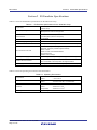
Table 2.1 shows the E8 Emulator specifications for the M16C/64 Group.
Table 2.1 E8 Emulator Specifications for the M16C/64 Group
M16C Family M16C/60 Series
Target MCUs
M16C/64 Group
Single-chip mode, Memory expansion mode
Available operating modes
* Microprocessor mode is not supported.
- Address match break, 4 points
Break functions
- PC break points (maximum 255 points)
Trace functions
None
Flash memory programming function
Available
User interface
Clock-synchronized serial (communication via P64/P65/P66/P67)
- Forced break
- ROM size: 3 KB (variable assigned address)
- RAM size: 128 bytes (variable assigned address)
- Stack 14 bytes
MCU resources to be used
- UART1 function and P64/P65/P66/P67
- Pins P50 and P55
- Address match interrupt
Emulator power supply
Unnecessary (USB bus powered, power supplied from the PC)
USB (USB 1.1, full speed)
Interface with host machine
* Also connectable to host computers that support USB 2.0
Power supply function
Can supply 3.3 V or 5.0 V to the user system (maximum 300 mA)
Power voltages
M16C/64
2.7 - 5.5 V (f(BCLK)=25MHz)
Table 2.2 shows the operating environment of the E8 emulator.
Table 2.2 Operating Environment
Temperatures
Humidity
Vibrations
Ambient gases
REJ10J1658-0100 Rev.1.00 Jan. 01, 2008
Page 3 of 34
Active
: 10°C to 35°C
Inactive
: –10°C to 50°C
Active
: 35% RH to 80% RH, no condensation
Inactive
: 35% RH to 80% RH, no condensation
Active
: maximum 2.45 m/s
Inactive
: maximum 4.9 m/s
Transportation
: maximum 14.7 m/s
No corrosive gases
2
2
2
E8 Emulator
REJ10J1658-0100 Rev.1.00 Jan. 01, 2008
Page 4 of 34
Section 2 E8 Emulator Specifications
E8 Emulator
Section 3 Connecting the E8 Emulator to the User System
Section 3 Connecting the E8 Emulator to the User System
Before connecting the E8 emulator to the user system, a connector must be installed in the user system so a user system
interface cable can be connected. When designing the user system, refer to Figure 4.1 “E8 Connecting Connector Pin
Assignments”, and Figures 5.1 to 5.4 “Example of an E8 Connection”.
Before designing the user system, be sure to read the E8 Emulator User’s Manual and related device hardware manuals.
Table 3.1 shows the recommended connector for the emulator.
Table 3.1 Recommended Connector
14-pin connector
Type Number
2514-6002
Manufacturer
3M Limited
Specification
14-pin straight type
Connect E8 connecting connector pins 2, 6, 10, 12 and 14 firmly to the GND on the user system board. These pins are
used as an electric GND and monitor the connection of the user system connector. Note the pin assignments for the user
system connector.
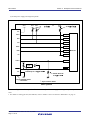
User system interface cable
Connector
User system
Pin 2
Pin 1
Figure 3.1 Connecting the User System Interface Cable with an E8 Connecting Connector
Notes:
1. Do not place any components within 3 mm area of the connector.
2. When using the E8 emulator as a programmer, connect it to the user system in the same way.
REJ10J1658-0100 Rev.1.00 Jan. 01, 2008
Page 5 of 34
E8 Emulator
REJ10J1658-0100 Rev.1.00 Jan. 01, 2008
Page 6 of 34
Section 3 Connecting the E8 Emulator to the User System
E8 Emulator
Section 4 E8 Connecting Connector Pin Assignments
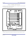
Section 4 E8 Connecting Connector Pin Assignments
Figure 4.1 shows the pin assignments for the E8 connecting connector.
Pin No.
Pin 1 mark
Connector
1
2
P65 (SCLK)
Vss
3
4
CNVss
P55 (EPM)
5
P67 (TxD)
6
Vss
P50 (CE)
7
Pin 2
Pin 14
Pin 1
Pin 13
Pin 1 mark
M16C/64
MCU signals
8
Vcc
9
P64 (BUSY)
10
11
Vss
P66 (RxD)
12
Vss
13
RESE T
Vss
14
Figure 4.1 E8 Connecting Connector Pin Assignments
Note:
Pin 14 is used for checking the connection between the E8 and the user system, and is not directly connected to the
Vss inside the E8. Make sure pins 2, 6, 10, 12 and 14 are all connected to the Vss.
REJ10J1658-0100 Rev.1.00 Jan. 01, 2008
Page 7 of 34
E8 Emulator
REJ10J1658-0100 Rev.1.00 Jan. 01, 2008
Page 8 of 34
Section 4 E8 Connecting Connector Pin Assignments
E8 Emulator
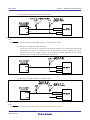
Section 5 Examples of E8 Connections
Section 5 Examples of E8 Connections
The following show connection examples. When using the emulator as a programmer, the connection specification
between the E8 and the MCUs is the same as shown below.
(1) In single power supply and single-chip mode
Figure 5.1 Example of an E8 Connection (Single Power Supply and Single-chip Mode)
Note:
1. For details on setting pins P50, P55, P64 and P65, refer to numbers 1 and 2 of “Points to Remember” on page 13.
REJ10J1658-0100 Rev.1.00 Jan. 01, 2008
Page 9 of 34
E8 Emulator
Section 5 Examples of E8 Connections
(2) In single power supply and memory expansion mode
Figure 5.2 Example of an E8 Connection (Single Power Supply and Memory Expansion Mode)
Notes:
1. For details on setting pins P64 and P65, refer to number 1 of “Points to Remember” on page 13.
2. The HOLD signal cannot be used. Pull up P55 on the user system.
3. P50 is used as the WRL#/WR# pin. The E8 emulator outputs “H” to the CE pin when going to boot mode (resetting
the MCU). In other cases, the CE pin is in a Hiz state. This prevents signal collision between the E8 emulator and
the MCU. The WRL#/WR# pin does not affect the memory because the pin has a low active signal.
REJ10J1658-0100 Rev.1.00 Jan. 01, 2008
Page 10 of 34
E8 Emulator
Section 5 Examples of E8 Connections
(3) In dual power supply and single-chip mode
Vcc1
Vcc1
Vcc1
Pulled up at 4.7k
Pulled up at
4.7k
Vcc2
Vcc
SCLK
P65 [*1]
RxD
P66
TxD
P67
BUSY
P64 [*1]
EPM
P55 [*1]
CE
M16C/64
P50
CNVss
CNVss
Vcc1
User
logic
*
RESET
RESET
Vss
Pulled up at 4.7k
Pulled down at
4.7k
14-pin 2.54mm pitch
connector
* : Open-collector buffer
User system
Figure 5.3 Example of an E8 Connection (Dual Power Supply and Single-chip Mode)
Note:
1. For details on setting pins P55, P64 and P65, refer to numbers 1 and 2 of “Points to Remember” on page 13.
REJ10J1658-0100 Rev.1.00 Jan. 01, 2008
Page 11 of 34
E8 Emulator
Section 5 Examples of E8 Connections
(4) In dual power supply and memory expansion mode
Pulled up at 4.7k
Pulled up at
4.7k or more
Vcc1 Vcc1
Vcc1
Vcc2
k
Vcc2
Pulled up at
4.7k or more
Vcc
SCLK
P65 [*1]
RxD
P66
TxD
P67
BUSY
P64 [*1]
EPM
P55 [*2]
CE
M16C/64
P50
CNVss
CNVss
Vcc 1
User
logic
*
RESET
RESET
Vss
Pulled up at 4.7k
or more
Pulled down at 4.7k
14-pin 2.54mm pitch connector
or more
* : Open-collector buffer
User system
Figure 5.4 Example of an E8 Connection (Dual Power Supply and Memory Expansion Mode)
Notes:
1. For details on setting pins P64 and P65, refer to numbers 1 and 2 of “Points to Remember” on page 13.
2. The HOLD signal cannot be used. Pull up P55 on the user system.
REJ10J1658-0100 Rev.1.00 Jan. 01, 2008
Page 12 of 34
E8 Emulator
Section 5 Examples of E8 Connections
Points to Remember
1. Pins P64, P65, P66 and P67 are used exclusively by the E8 emulator. Connect the E8 emulator to the MCU pins.
Connect pins P66 and P67 to the E8a emulator after pulling up the MCU pins at the Vcc (Vcc1) level. For P64 and
P65, pull up the pins at the Vcc (Vcc1) level or pull down them according to the MCU pin state after disconnecting
the E8 emulator. P64 may be in a Hiz state while the E8 emulator is active. Therefore, set the pin resistance value so
the voltage cannot be at the midpoint potential, depending on the voltage dividing of the resistance inside the E8
emulator (Figure 5.12).
Figure 5.5 E8 Emulator and MCU Connection
2. The E8 emulator uses pins P50 and P55 for MCU control. Connect the E8 emulator to the MCU pins.
(1) In single power supply and single-chip mode
For P50 and P55, pull up the pins at the Vcc level or pull down them according to the MCU pin state
after disconnecting the E8 emulator. P50 and P55 may be in a Hiz state while the E8 emulator is
active. Therefore, set the pin resistance value so the voltage cannot be at the midpoint potential,
depending on the voltage dividing of the resistance inside the E8 emulator (Figure 5.12).
Figure 5.6 Connection of E8 Emulator and Pins P50 and P55 (Single Power Supply and Single-chip Mode)
REJ10J1658-0100 Rev.1.00 Jan. 01, 2008
Page 13 of 34
E8 Emulator
Section 5 Examples of E8 Connections
(2) Single power supply and memory expansion mode
Figure 5.7 Connection of E8 Emulator and Pins P50 and P55 (Single Power Supply and Memory Expansion Mode)
Note:
1. The HOLD signal cannot be used. Pull up P55 at the Vcc level on the user system.
(3) In dual power supply and single-chip mode
Pull up P55 at the Vcc2 level or pull down it according to the MCU pin state after disconnecting the
E8 emulator. P55 may be in a Hiz state while the E8 emulator is active. Therefore, set the pin
resistance value so the voltage cannot be at the midpoint potential, depending on the voltage
dividing of the resistance inside the E8 emulator (Figure 5.12).
Figure 5.8 Connection of E8 Emulator and Pins P50 and P55 (Dual Power Supply and Single-chip Mode)
(4) In dual power supply and memory expansion mode
Figure 5.9 Connection of E8 Emulator and Pins P50 and P55 (Dual Power Supply and Memory Expansion Mode)
Note:
1. The HOLD signal cannot be used. Pull up P55 at the Vcc2 level on the user system.
REJ10J1658-0100 Rev.1.00 Jan. 01, 2008
Page 14 of 34
E8 Emulator
Section 5 Examples of E8 Connections
3. The E8 emulator uses the CNVss pin for MCU control. Pull down the E8 emulator and MCU pins and connect the
E8 emulator.
Figure 5.10 E8 Emulator and CNVss Pin Connection
4. The RESET pin is used by the E8 emulator. Therefore, use an open-collector output buffer or a CR reset circuit as
the reset circuit for the user system. The recommended pull-up value is 4.7 kΩ or more. The MCU can be reset by
outputting “L” from the E8 emulator. However, if the reset IC output is “H”, the user system reset circuit cannot be
set to “L”. As such, the E8 emulator will not operate normally.
Vcc
User system
connector
RESET
User
logic
*
13
RESET
M16C/64
Pulled up at
4.7k or more
* : Open-collector buffer
Figure 5.11 Example of a Reset Circuit
5.
6.
7.
8.
Connect Vss and Vcc to the Vss and Vcc (Vcc1) of the MCU, respectively.
The amount of voltage input to Vcc (Vcc1, Vcc2) must be within the specified range of the MCU.
If NMI interrupts are not used, make sure the NMI pin is pulled up to the Vcc (Vcc1) pin through a resistor.
Pin 14 is used for checking the connection between the E8 and the user system, and is not directly connected to the
Vss inside the E8. Make sure that pins 2, 6, 10, 12 and 14 are all connected to the Vss.
REJ10J1658-0100 Rev.1.00 Jan. 01, 2008
Page 15 of 34
E8 Emulator
Section 5 Examples of E8 Connections
9. Figure 5.12 shows the interface circuit in the E8 emulator. Use this figure as a reference when determining the pullup resistance value.
User system connector
Vcc
Power supply circuit
(use only with power supply mode)
8
74LVC125A
Emulator control circuit
[*1]
22Ω
SCLK
22Ω
CNVss
3
22Ω
EPM
4
22Ω
CE
22Ω
RxD
1
7
11
100kΩ
100kΩ
74LVC125A
22Ω
TxD
22Ω
BUSY
22Ω
RESET
5
9
13
3.3V
10kΩ
2SC2462
10kΩ
[*1] Power for the upper 74LVC125A is supplied from Vcc in the user system connector or power supply circuit (in power supply mode).
Figure 5.12 Interface Circuit Inside the E8 Emulator (For Reference)
REJ10J1658-0100 Rev.1.00 Jan. 01, 2008
Page 16 of 34
E8 Emulator
Section 6 Notes on Using the E8 Emulator
Section 6 Notes on Using the E8 Emulator
1.
Program area for the E8 emulator
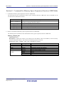
Table 6.1 lists the program areas allotted for the E8 emulator. Do not change this area allocation, otherwise the E8
emulator will not control the MCU. If settings were changed, disconnect the debugger and then reconnect it.
Table 6.1 Program Area for the E8 Emulator
ROM Size
Group
Part No.
Programming
Programming
Area 1
Area 2
Data Area
RAM
Size
Program Area for E8 Emulator
Vector Area
ROM Area
RAM
Area
3 KB of the
programming
area [*1]
128
bytes
[*1]
FFFE4h - FFFE7h,
M16C/64
R5F3640D
256 KB
16 KB
4 KB
(2 blocks)
FFFE8h - FFFEBh,
16 KB
FFFECh - FFFEFh,
FFFF4h - FFFF7h,
FFFFCh - FFFFFh
Note:
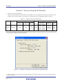
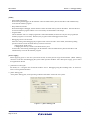
1. When starting the debugger, the [Emulator Setting] dialog box shown in Figure 6.1 is displayed. Specify the area which will not be used
in the user system. The data area cannot be specified.
Figure 6.1 [Firmware Location] Tab of the [Emulator Setting] Dialog Box
2. When the system is launched, the E8 emulator initializes the general registers and some of the flag registers as
shown in Table 6.2.
REJ10J1658-0100 Rev.1.00 Jan. 01, 2008
Page 17 of 34
E8 Emulator
Section 6 Notes on Using the E8 Emulator
Table 6.2 E8 Emulator Register Initial Values
Status
Register
Initial Value
PC
Reset vector value in the vector address table
R0 to R3 (bank 0, 1) 0000h
A0, A1 (bank 0, 1)
0000h
FB
(bank
0,
1)
0000h
E8
Emulator INTB
0000h
Activation USP
0000h
ISP
Work RAM Address for the E8 emulator + 80h [*1]
SB
0000h
FLG
0000h
Note:
1. The Work RAM address for the E8 emulator is specified in the [Firmware Location]
tab of the [Emulator Setting] dialog box.
3. The E8 emulator controls the MCUs by using the P50, P55, P64, P65, P66, P67, RESET and CNVss pins.
4. The E8 emulator uses up to 14 bytes of the stack pointer during a user program break. Therefore, set aside 14 bytes
for the stack area.
5.
SFRs used by the E8 emulator program
As the SFRs listed in Table 6.3 are used by the E8 emulator program, do not change any of these values. If these
values are changed, the E8 emulator cannot control the MCU. Note that UART1 transmit interrupt control register
S1TIC and UART1 receive interrupt control register S1RIC always read out values used by the emulator. These
registers are not initialized by selecting [Debug] -> [Reset CPU] or by using the RESET command. If register
contents are referred to, a value that has been set in the E8 emulator program will be read out.
Table 6.3 SFRs Used by the E8 Emulator Program
Address
Register
Symbol
Bit
Notes on Using
the E8 Emulator
020Eh
Address match interrupt enable register
AIER
All bits
[*1]
020Fh
Address match interrupt enable register 2
AIER2
All bits
[*1]
0210h - 0212h
Address match interrupt register 0
RMAD0
All bits
[*1]
0214h - 0216h
Address match interrupt register 1
RMAD1
All bits
[*1]
0218h - 021Ah
Address match interrupt register 2
RMAD2
All bits
[*1]
021Ch - 021Eh
0250h
Address match interrupt register 3
UART transmit/receive control register 2
RMAD3
UCON
All bits
Bits 1, 3, 4, 5 and 6
[*1]
[*2]
0258h
UART1 transmit/receive mode register
U1MR
All bits
[*1]
025Ah, 025Bh
UART1 transmit buffer register
U1TB
All bits
[*1]
025Ch
UART1 transmit/receive control register 0
U1C0
All bits
[*1]
025Dh
UART1 transmit/receive control register 1
U1C1
All bits
[*1]
025Eh, 025Fh
UART1 receive buffer register
U1RB
All bits
[*1]
03ECh
Port P6 register
P6
Bits 4, 5, 6 and 7
[*2]
03EEh
Port P6 direction register
PD6
Bits 4, 5, 6 and 7
[*2]
Notes:
1. Do not change this register value.
2. Do not change the value of the bits listed in the column to the left. When operating this register, make changes using the
bit operation instructions to avoid changing the bit values.
6.
Interrupts used by the E8 emulator program
REJ10J1658-0100 Rev.1.00 Jan. 01, 2008
Page 18 of 34
E8 Emulator
Section 6 Notes on Using the E8 Emulator
The BRK instruction interrupt, address match interrupt, single-step interrupt and DBC interrupt are used by the E8
emulator program. Therefore, make sure the user program does not use any of these interrupts. The E8 emulator
changes these interrupt vector values to the values to be used by the emulator. No problems occur if the interrupt
vector values are written in the user program.
7.
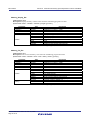
Debugging using the watchdog timer
When debugging the user program using the watchdog timer, click the [Debugging of program that uses WDT.]
check box in the [Firmware Location] tab of the [Emulator Setting] dialog box. By clicking this box, the E8
emulator program refreshes the watchdog timer during program operation. If memory access is executed through
memory reference or modification, the watchdog timer will be refreshed by the E8 emulator program. Note that
this timing will differ from the actual operational timing.
Figure 6.2 [Firmware Location] Tab of the [Emulator Setting] Dialog Box
REJ10J1658-0100 Rev.1.00 Jan. 01, 2008
Page 19 of 34
E8 Emulator
8.
Section 6 Notes on Using the E8 Emulator
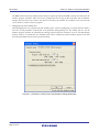
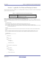
Flash memory ID code
This MCU function prevents the Flash memory from being read out by anyone other than the user. The ID code in
Table 6.4 written to the flash memory of the MCU must match the ID code displayed in the Figure 6.3 [ID Code
verification] dialog box at debugger startup, otherwise the debugger cannot be launched. Note that when the ID
code is FFh, FFh, FFh, FFh, FFh, FFh, FFh, the ID code is regarded as undefined. In this case, the ID code is
automatically authenticated and the [ID Code verification] dialog box is not displayed.
In ‘Program Flash’ mode, the contents of the user program are input into the ID code area. When debugging in
other modes, FFh, FFh, FFh, FFh, FFh, FFh, FFh is written into the ID code area regardless of the contents of the
downloaded user program.
Table 6.4 ID Code Storage Area of M16C/64
Address
FFFDFh
FFFE3h
FFFEBh
FFFEFh
FFFF3h
FFFF7h
FFFFBh
Description
First byte of ID code
Second byte of ID code
Third byte of ID code
Fourth byte of ID code
Fifth byte of ID code
Sixth byte of ID code
Seventh byte of ID code
Figure 6.3 [ID Code verification] Dialog Box
Note on ‘Program Flash’ mode:
When the ID code is specified by the -ID option of the lmc30, download the MOT file or HEX file. When the X30 file
is downloaded, the ID code is not valid. When downloading the X30 file, specify the ID code using an assembler
directive command such as “.BYTE”. The file to which the ID code specified by the assembler directive command
“.ID” is output varies depending on the version of the assembler. For details, refer to the Assembler User’s Manual.
9.
Reset
The reset vector is used by the E8 emulator program. If the MCU is reset while executing the user program, control
is transferred to the E8 emulator program and the user program is forced to stop. Do not use the hardware reset 2,
software reset, watchdog timer reset and oscillation stop detection reset, otherwise the E8 emulator will not operate
normally.
REJ10J1658-0100 Rev.1.00 Jan. 01, 2008
Page 20 of 34
E8 Emulator
Section 6 Notes on Using the E8 Emulator
10. Memory access during emulation execution
When referring to or modifying the memory contents, the user program is temporarily halted. For this reason, a
real-time emulation cannot be performed. When a real-time emulation is necessary during a program execution,
disable the automatic update in the watch window or fix the display in the memory window before running the
program so that memory accesses do not occur during an execution.
11. When the E8 emulator does not supply power to the user system, it consumes the power voltage of the user system
from several mA to more than 10 mA. This is because the user power supply drives one 74LVC125A to make the
communication signal level match the user system power supply voltage.
12. When debugging, the Flash memory is frequently rewritten by the E8 emulator. Therefore, do not use an MCU that
has been used for debugging in products. Also, as the E8 emulator program is written to the MCU while debugging,
do not save the contents of the MCU Flash memory which were used for debugging nor use them as the ROM data
for products.
13. NMI interrupt
If NMI interrupts are used, be sure to take the necessary precautions before executing the user program like
disabling the automatic update in the watch window or fix the display in the memory window before running the
program so that memory accesses do not occur during an execution. If an NMI interrupt occurs while the user
program halts or when memory contents are referenced or modified during user program execution, the E8
emulator cannot control the MCU.
14. Reserved area
The addresses not specified in the Hardware Manual for M16C/64 Group are reserved area. Do not change the
contents. Otherwise, the E8 emulator cannot control the MCU.
15. Debugging in stop mode or wait mode
When in stop mode or wait mode, the program cannot be stopped by the E8 emulator. If you attempt to stop the
program in stop or wait mode, the emulator will not control the MCU. Do not operate windows until the program
stops at the breakpoint by setting the breakpoint at the line of the program where the stop mode or the wait mode is
cancelled. When using stop mode or wait mode in the user program, disable the automatic update in the watch
window or fix the display in the memory window before running the program so memory accesses do not occur
during an execution.
16. Peripheral I/Os during a halt
During a user program halt, interrupts are not accepted although peripheral I/Os continue to run. For example, a
timer interrupt is not accepted although the timer continues to count when a user program is stopped by a break
after the timer started.
REJ10J1658-0100 Rev.1.00 Jan. 01, 2008
Page 21 of 34
E8 Emulator
Section 6 Notes on Using the E8 Emulator
17. Exceptional step execution
a) Software interrupt instruction
Step execution cannot be performed in the internal processing of instructions (undefined, overflow, BRK and
INT) which generate a software interrupt continuously in the program.
Example: INT instruction
NOP
NOP
INT #3
NOP
JMP MAIN
INT_3:
NOP
NOP
NOP
REIT
Passes through if the STEP execution is carried out.
Program should be stopped at this address.
b) INT instruction
To debug the user program with the INT instruction, set a PC break for the internal processing of the INT
instruction and execute the program with the GO command.
Example:
NOP
INT #3
NOP
JMP MAIN
Execute using GO command.
INT_3:
NOP Break
NOP
REIT
18. “Go to cursor” function
The “Go to cursor” function is actualized using an address match break. Therefore, when you execute the “Go to
cursor” command, all the address match breaks you set become invalid, while all the PC breaks remain valid.
19. Note on PC break point
When downloading a user program after modifying it, the set address of PC break may not be corrected normally
depending on the modification. Therefore, break points other than the set PC breaks may shift. After downloading
a user program, check the setting of PC breaks in the event point window and reset it.
If the 125kHz on-chip oscillator or sub clock is used as the operation clock of the MCU, setting or canceling PC
breaks may take time. Use event breaks as the first choice.
REJ10J1658-0100 Rev.1.00 Jan. 01, 2008
Page 22 of 34
E8 Emulator
Section 6 Notes on Using the E8 Emulator
20. Note on debugging in CPU rewrite mode
When debugging in CPU rewrite mode, do not rewrite in CPU block 0 area (addresses F0000h - FFFFFh) and
block containing the E8 emulator program. If these areas are rewritten, the E8 emulator will not control the MCU.
Do not halt the user program while setting up the CPU rewrite mode and releasing it. If halted, the E8 emulator
may not control the MCU. In addition, disable the automatic update in the watch window or fix the display in the
memory window before running the program so memory accesses do not occur during an execution.
To check the data after executing the CPU rewrite mode, halt the program after releasing the CPU rewrite mode
and refer to the memory window, etc.
When rewriting the Flash memory in the program area, select Menu -> [Setup] -> [Emulator] -> [System...] to
open the [Configuration] dialog box in the High-performance Embedded Workshop. In this dialog box, change the
[Flash memory synchronization] setting to [Flash memory to PC] and set the debugger cache to OFF. In this setting,
the Flash memory is read whenever a break occurs, which takes some time. Use it with the [Disable] setting except
when debugging in CPU rewrite mode.
21. Note on lock bits of Flash memory
When starting up in the [Erase Flash and Connect] mode or [Program Flash] mode, lock bits in all the blocks of the
Flash memory will be unlocked. Note that the lock bits of the downloaded blocks will be unlocked after
downloading the user program.
22. Notes on rewriting Flash memory
Do not reset the MCU when rewriting the Flash memory.
The Flash memory is rewritten when the “Flash memory write end” is displayed in the output window of the Highperformance Embedded Workshop. If the MCU is reset when rewriting the Flash memory, the user program or the
E8 emulator program may be disrupted.
Flash memory rewrite occurs:
- When downloading the user program
- After setting PC breaks in the Flash memory and executing the user program
- After canceling PC breaks in the Flash memory and executing the user program
- After rewriting the value of the Flash memory in the memory window and executing the user program
23. Notes on the E8 emulator power supply
When writing a program with the E8 emulator for mass production processes, the program requires reliability, so
do not use the E8 emulator power supply function. Supply power separately to the user system according to the
allowable voltage for MCU writing. Voltage supplied from the E8 emulator depends on the quality of the USB
power supply of the PC, and as such, precision is not guaranteed. Note that when debugging the system which
operates the MCU with a dual power supply, power cannot be supplied from the E8.
24. Notes on the emulator setup switch
Use the emulator setup switch at the factory setting (upper side 1).
25. Notes on downloading the user program
When the user program is downloaded, the operation clock is switched to Xin. After the download completed, the
CPU is reset. Therefore, the CPU is always reset whether the "Reset CPU after download module" checkbox in the
[Options] tab of the [Debug Settings] dialog box is selected or not. To open the dialog box, select the [Debug]
menu -> [Debug Settings].
REJ10J1658-0100 Rev.1.00 Jan. 01, 2008
Page 23 of 34
E8 Emulator
REJ10J1658-0100 Rev.1.00 Jan. 01, 2008
Page 24 of 34
Section 6 Notes on Using the E8 Emulator
E8 Emulator
Section 7 Debugger Setting
Section 7 Debugger Setting
1. [Emulator Setting] dialog box
The [Emulator Setting] dialog box is provided for setting items that need to be set when the debugger is launched.
The contents set from this dialog box (excluding [Power Supply] group box items) also become valid the next time
the debugger is launched. When launching the debugger for the first time after creating a new project work space,
the [Emulator Setting] dialog box is displayed with the Wizard.
Figure 7.1 [Emulator Setting] Dialog Box
If you check “Do not show this dialog box again.” at the bottom of the [Emulator Setting] dialog box, the [Emulator
Setting] dialog box will not be displayed the next time the debugger is launched. You can open the [Emulator
Setting] dialog box using one of the following methods:
- After the debugger is launched, select Menu -> [Setup] -> [Emulator] -> [Emulator Setting...].
- Hold down the Ctrl key while launching the debugger.
When “Do not show this dialog box again.” is checked, the E8 does not supply power to the user system.
REJ10J1658-0100 Rev.1.00 Jan. 01, 2008
Page 25 of 34
E8 Emulator
Section 7 Debugger Setting
2. [Emulator mode] tab
Device selection, mode specification and power supply setting are made from the [Emulator mode] tab of the
[Emulator Setting] dialog box.
Figure 7.2
[Emulator mode] Tab
[MCU Group]
Select the name of the MCU group to be used from the [MCU Group] drop-down list.
[Device]
Select the type of MCU to be used from the [Device] drop-down list.
REJ10J1658-0100 Rev.1.00 Jan. 01, 2008
Page 26 of 34
E8 Emulator
Section 7 Debugger Setting
[Mode]
- Erase Flash and Connect
When starting the debugger, the E8 emulator erases the Flash memory data for the MCUs and simultaneously
writes the E8 emulator program.
- Keep Flash and Connect
When launching the debugger, the E8 emulator retains the Flash memory data for the MCUs. Note that the area
for the E8 emulator program and the vector area used by the E8 emulator will change.
- Program Flash
The E8 emulator starts as a simple programmer. When downloaded, the E8 writes only the user program (E8
emulator program is not written). Therefore, the program cannot be debugged in this mode.
- Debugging of CPU rewrite mode
Select this setting when debugging the program which rewrites the CPU. In this mode, the following debug
operation which rewrites the Flash memory cannot be executed.
- Setting the PC break points
- Changing the memory contents in the Flash memory area
In this mode, when starting the debugger, the E8 emulator erases the Flash memory data for the MCUs and
simultaneously writes the E8 emulator program.
[Power supply]
When supplying power to the user system from the E8, click the [Power Target from Emulator. (MAX 300mA)]
check box. Note that when debugging the system which operates the MCU with a dual power supply, power cannot
be supplied from the E8.
3. [Firmware Location] tab
For details, see “1. Program area for the E8 emulator” and “7. Debugging using the watchdog timer” in “Section 6.
Notes on Using the E8 Emulator”.
4. [MCU Setting] Tab
In the [MCU Setting] tab, set the operating condition of the MCU used in the user system.
Figure 7.3 [MCU Setting] Tab
REJ10J1658-0100 Rev.1.00 Jan. 01, 2008
Page 27 of 34
E8 Emulator
Section 7 Debugger Setting
Specify processor mode
Specify the processor mode according to the user system. One of the following can be specified:
- Single-Chip Mode
- Memory Expansion Mode
Memory Expansion Mode
When Memory Expansion Mode is selected, specify whether the memory space expansion function will be used.
When using the memory space expansion function, select “4 MB Mode”, and when not using, select “Normal
Mode”.
PM13 (b3 of 000005H) is ‘1’
Specify whether PM13 (third bit of processor mode register 1) is set. When using the user program with PM13 set
to “1”, check this option.
PM10 (b0 of 000005H) is ‘1’
Specify whether PM10 (zero bit of processor mode register 1) is set. When using the user program with PM10 set
to “1”, check this option.
PRG2C0 (b0 of 000010H) is ‘1’
Specify whether PRG2C0 (zero bit of program 2 area control register) is set. When using the user program with
PRG2C0 set to “1”, check this option.
Notes:
The following describes precautions to be taken when using the emulator in memory expansion mode:
- When the external area cannot be rewritten via normal memory access, software breaks cannot be used in that area.
- No address match break can be used in the external memory space.
- The “Go to Cursor” function cannot be used in the external memory space. If this function is used in the external
memory space, the program will be in a state of execution.
- To access the memory space expansion area in the download, the editor window (MIX display or disassembled
display mode), the memory window or the watch window while operating in the memory space expansion 4 MB
mode, be aware that only bank 7 can be accessed. In this case, the data bank offset depends on the offset bits of the
data bank register.
- When using the memory space expansion function 4 MB mode, execute the command for the memory space
expansion function 4 MB mode to access each bank.
REJ10J1658-0100 Rev.1.00 Jan. 01, 2008
Page 28 of 34
E8 Emulator
Section 8 Command for Memory Space Expansion Function 4 MB Mode
Section 8 Command for Memory Space Expansion Function 4 MB Mode
1. Command for Memory Space Expansion Function 4 MB Mode
The following show the command for memory space expansion function 4 MB mode. These commands can be
executed in the command line window.
Command
Memory_Compare_Ext
Memory_Display_Ext
Memory_Fill_Ext
Memory_Find_Ext
Memory_Move_Ext
Description
Compares the memory area (between the start address and the end address) with
the memory starting at destination address.
Displays memory contents.
Fills an area of memory.
Finds a string in a memory range.
Moves memory.
2. Details of Command for Memory Space Expansion Function 4 MB mode
The following show the details of the command for memory space expansion function 4 MB mode.
Memory_Compare_Ext
Abbreviation: MCE
Description: Compares the memory area (between the start address and the end address) with the memory
starting at destination address. This cannot be used during program execution.
Syntax: MCE <bank> <offsetbit> <start> <end> <destination> [<mode>]
Parameter
<bank>
<offsetbit> *
<start>
<end>
<destination>
Type
Description
Numeric
Bank (0 – 7)
Numeric
Offset bit (0: no offset, 1: offset)
Numeric
Start address
Numeric
End address (including this address)
Numeric
Destination address
Keyword
Format (optional, default = BYTE)
BYTE
1 byte
<mode>
WORD
2 bytes
LONG
4 bytes
DOUBLE
8 bytes
*: When “PM13 is 1” is not selected in the MCU setting dialog box, set the offset bit to “0”.
REJ10J1658-0100 Rev.1.00 Jan. 01, 2008
Page 29 of 34
E8 Emulator
Section 8 Command for Memory Space Expansion Function 4 MB Mode
Memory_Display_Ext
Abbreviation: MDE
Description: Displays memory contents. This cannot be used during program execution.
Syntax: MDE <bank> <offsetbit> <address> [<length>] [<mode>]
Parameter
<bank>
<offsetbit> *
<address>
<length>
Type
Description
Numeric
Bank (0 – 7)
Numeric
Offset bit (0: no offset, 1: offset)
Numeric
Start address
Numeric
Length (optional, default = 0x100 bytes)
Keyword
Display format (optional, default = BYTE)
BYTE
Bytes
WORD
Words (2 bytes)
<mode>
LONG
Long words (4 bytes)
ASCII
ASCII
SINGLE
Single-precision floating-point (4 bytes)
DOUBLE
Double-precision floating-point (8 bytes)
*: When “PM13 is 1” is not selected in the MCU setting dialog box, set the offset bit to “0”.
Memory_Fill_Ext
Abbreviation: MFE
Description: Fills an area of memory. This cannot be used during program execution.
Syntax: MFE <bank> <offsetbit> <start> <end> <data> [<mode>] [<verify>]
Parameter
<bank>
<offsetbit> *
<start>
<end>
<data>
Type
Description
Numeric
Bank (0 – 7)
Numeric
Offset bit (0: no offset, 1: offset)
Numeric
Start address
Numeric
End address
Numeric
Data value
Keyword
Data size (optional, default = BYTE)
BYTE
Byte
WORD
Word (2 bytes)
<mode>
LONG
Long word (4 bytes)
ASCII
ASCII
SINGLE
Single-precision floating-point (4 bytes)
DOUBLE
Double-precision floating-point (8 bytes)
Keyword
Verify flag (optional, default = V)
<verify>
V
Verification
N
No verification
*: When “PM13 is 1” is not selected in the MCU setting dialog box, set the offset bit to “0”.
REJ10J1658-0100 Rev.1.00 Jan. 01, 2008
Page 30 of 34
E8 Emulator
Section 8 Command for Memory Space Expansion Function 4 MB Mode
Memory_Find_Ext
Abbreviation: MIE
Description: Finds a string in a memory range. This cannot be used during program execution.
Syntax: MIE <bank> <offsetbit> <start> <end> <string> [<mode>]
Parameter
<bank>
<offsetbit> *
<start>
<end>
<string>
Type
Description
Numeric
Bank (0 – 7)
Numeric
Offset bit (0: no offset, 1: offset)
Numeric
Start address
Numeric
End address (including this address)
Numeric
String to search for
Keyword
Format (optional, default = BYTE)
BYTE
Bytes
WORD
Words (2 bytes)
<mode>
LONG
Long words (4 bytes)
ASCII
ASCII
SINGLE
Single-precision floating-point (4 bytes)
DOUBLE
Double-precision floating-point (8 bytes)
*: When “PM13 is 1” is not selected in the MCU setting dialog box, set the offset bit to “0”.
Memory_Move_Ext
Abbreviation: MVE
Description: Moves memory. This cannot be used during program execution.
Syntax: MVE <bank> <offsetbit> <start> <end> <destination> [<verify>] [<mode>]
Parameter
<bank>
<offsetbit> *
<start>
<end>
<destination>
Type
Description
Numeric
Bank (0 – 7)
Numeric
Offset bit (0: no offset, 1: offset)
Numeric
Source start address
Numeric
Source end address (including this address)
Numeric
Destination start address
Keyword
Verify flag (optional, default = V)
<verify>
V
Verification
N
No verification
Keyword
Format (optional, default = BYTE)
BYTE
1 byte
<mode>
WORD
2 bytes
LONG
4 bytes
DOUBLE
8 bytes
*: When “PM13 is 1” is not selected in the MCU setting dialog box, set the offset bit to “0”.
REJ10J1658-0100 Rev.1.00 Jan. 01, 2008
Page 31 of 34
E8 Emulator
REJ10J1658-0100 Rev.1.00 Jan. 01, 2008
Page 32 of 34
Section 8 Command for Memory Space Expansion Function 4 MB Mode
E8 Emulator
Section 9 Applicable Tool Chain and Third-party Products
Section 9 Applicable Tool Chain and Third-party Products
With the M16C/64 Group E8 emulator, you can debug modules created by the inhouse tool chain and third-party
products listed in Table 9.1 below.
Table 9.1 Applicable Tool Chain and Third-party Products
Tool chain
Third-party products
M3T-NC30WA V.5.20 Release 01 or later
TASKING M16C C/C++/EC++ Compiler V.2.3r1 or later
IAR EWM16C V.2.12 or later
Notes on debugging the load modules created in ELF/DWARF2 format:
If the load module was created in ELF/DWARF2 format using TASKING M16C C/C++/EC++ compiler V3.0r1, the
precautionary note described below must be observed when displaying member variables of the base class in the watch
window.
Precautionary Note:
If any class object with a base class is defined, the following problems may occur:
Case 1: Member variables of the base class cannot be referenced directly from the class object (*1).
Case 2: If the PC value resides in any member function of a derived class, member variables of the base class cannot
be referenced directly (*4).
Solution:
If member variables of the base class need to be referenced in the watch window, follow either method described
below:
Case 1: Use indirect references from the class object to refer to member variables of the base class (*2) (*3).
Case 2: Use indirect references from “this” pointer to refer to member variables of the base class (*5) (*6).
<Example code>
/////////////////////////////////////////////////////////
*.h
class BaseClass
{
public:
int m_iBase;
public:
BaseClass() {
m_iBase = 0;
}
void BaseFunc(void);
};
class DerivedClass : public BaseClass
{
public:
int m_iDerive;
public:
DerivedClass() {
m_iDerive = 0;
}
void DerivedFunc(void);
};
REJ10J1658-0100 Rev.1.00 Jan. 01, 2008
Page 33 of 34
E8 Emulator
Section 9 Applicable Tool Chain and Third-party Products
*.cpp
main()
{
class DerivedClass ClassObj;
ClassObj.DerivedFunc();
return;
}
void BaseClass::BaseFunc(void)
{
m_iBase = 0x1234;
}
void DerivedClass::DerivedFunc(void)
{
BaseFunc();
m_iDerive = 0x1234;
}
/////////////////////////////////////////////////////////
< Watch window registration example>
/////////////////////////////////////////////////////////
Case 1: If the PC value resides in the main() function
(1)"ClassObj.m_iBase"
: Cannot be referenced (*1)
(2)"ClassObj.__b_BaseClass.m_iBase" : Can be referenced (*2)
(3)"ClassObj"
-"__b_BaseClass"
-"m_iBase"
: Can be referenced (*3)
-"m_iDerive"
-: Expansion symbol
Case 2: If the PC value resides in the DerivedClass::DerivedFunc() function
(1)"m_iBase"
: Cannot be referenced (*4)
(2)"this->__b_BaseClass.m_iBase" : Can be referenced (*5)
(3)"__b_BaseClass.m_iBase": Can be referenced (*5)
(4)"this"
-"*"
-"__b_BaseClass"
-"m_iBase"
: Can be referenced (*6)
-"m_iDerive"
(5)"__b_BaseClass"
-"m_iBase"
: Can be referenced (*6)
/////////////////////////////////////////////////////////
REJ10J1658-0100 Rev.1.00 Jan. 01, 2008
Page 34 of 34
E8 Emulator
Additional Document for User's Manual
Notes on Connecting the M16C/64
Publication Date:
Jan. 01, 2008
Rev.1.00
Published by:
Sales Strategic Planning Div.
Renesas Technology Corp.
Edited by:
Microcomputer Tool Development Department
Renesas Solutions Corp.
© 2008. Renesas Technology Corp. and Renesas Solutions Corp., All rights reserved. Printed in Japan.
E8 Emulator
Additional Document for User’s Manual
1753, Shimonumabe, Nakahara-ku, Kawasaki-shi, Kanagawa 211-8668 Japan
REJ10J1658-0100