1
LE
AVAILAB
78M6613 Split-Phase
Firmware Description Document
December 2011
Rev. 2
UG_6613_090
78M6613 Split-Phase Firmware Description Document
UG_6613_090
Maxim cannot assume responsibility for use of any circuitry other than circuitry entirely embodied in a Maxim product. No circuit patent licenses are implied.
Maxim reserves the right to change the circuitry and specifications without notice at any time. The parametric values (min and max limits) shown in the Electrical
Characteristics table are guaranteed. Other parametric values quoted in this data sheet are provided for guidance.
Maxim Integrated 160 Rio Robles, San Jose, CA 95134 USA 1-408-601-1000
© Maxim Integrated
The Maxim logo and Maxim Integrated are trademarks of Maxim Integrated Products, Inc.
UG_6613_090
78M6613 Split-Phase Firmware Description Document
Table of Contents
1
Introduction ................................................................................................................................... 5
1.1 Terminology ............................................................................................................................. 5
1.2 Hardware Assignments ............................................................................................................ 6
1.2.1 Fixed Reference Sensor Configuration ........................................................................ 6
1.2.2 Floating Reference Sensor Configuration .................................................................... 7
1.3 Measurement Equations .......................................................................................................... 9
1.4 Sampling and Update Rates .................................................................................................... 9
2
Functional Description ................................................................................................................ 10
2.1 Initialization and Start-up........................................................................................................ 10
2.2 Sensor (Hardware) Configuration ........................................................................................... 10
2.3 AC Measurement and Monitoring ........................................................................................... 10
2.4 Configuration and Control ...................................................................................................... 12
2.4.1 Input Registers .......................................................................................................... 12
2.4.2 Calibration ................................................................................................................. 12
2.4.3 Relay Control ............................................................................................................ 14
2.4.3.1 TC Command .............................................................................................. 15
2.4.4 Sag Detection Settings .............................................................................................. 16
2.4.5 Creep Thresholds ...................................................................................................... 16
2.4.6 Limit Registers (Alarms) ............................................................................................ 16
3
Split-Phase M-API Register Map ................................................................................................. 17
3.1 Output Registers .................................................................................................................... 17
3.2 Input Registers....................................................................................................................... 19
3.3 CE Parameters ...................................................................................................................... 22
4
Serial Communication ................................................................................................................. 24
4.1 CLI Firmware Application ....................................................................................................... 24
4.2 SLIP Firmware Application ..................................................................................................... 24
5
Contact Information ..................................................................................................................... 24
Appendix A – Command Line Interface .............................................................................................. 25
A.1 Identification Command ......................................................................................................... 25
A.2 Reset Commands .................................................................................................................. 25
A.3 Data Access Commands........................................................................................................ 26
A.3.1 Individual Address Read ............................................................................................ 26
A.3.2 Consecutive Read ..................................................................................................... 26
A.3.3 Block Reads .............................................................................................................. 26
A.3.4 Concatenated Reads ................................................................................................. 27
A.3.5 Repeat Command ..................................................................................................... 27
A.3.6 CE Data Access ........................................................................................................ 28
A.4 Write Commands ................................................................................................................... 29
A.4.1 MPU Register Write Commands ................................................................................ 29
A.4.2 CE Register Write Commands ................................................................................... 29
A.5 Calibration Commands........................................................................................................... 29
A.5.1 Complete Calibration Command ................................................................................ 29
A.5.2 Atomic Calibration Commands .................................................................................. 30
Appendix B – SLIP Interface ............................................................................................................... 31
B.1 Packet Format and Definition ................................................................................................. 31
B.1.1 Packet Format ........................................................................................................... 31
B.1.2 Start and End ............................................................................................................ 31
B.1.3 Device Address ......................................................................................................... 31
B.1.4 Data .......................................................................................................................... 32
B.1.5 CRC-8 ....................................................................................................................... 32
Rev. 2
3
78M6613 Split-Phase Firmware Description Document
UG_6613_090
B.2 Packet Types ......................................................................................................................... 32
Example 1 – Read Command Packet ..................................................................................... 37
Example 2 – Write Command Packet ..................................................................................... 37
Example 3 – Contiguous Block Read Command Packet ......................................................... 37
Example 4 – Contiguous Block Write Command Packet ......................................................... 38
Example 5 – Device Information Command Packet ................................................................ 38
Example 6 – CLI Toggle Command Packet ............................................................................ 38
B.3 Command Registers .............................................................................................................. 39
Revision History .................................................................................................................................. 40
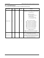
Figures
Figure 1: Simplified Connection Diagram with Fixed Reference ................................................................ 6
Figure 2: Simplified Connection Diagram with Floating Reference ............................................................ 7
Figure 3: Simplified Signal Processing Flow ........................................................................................... 11
Figure 4: Split-Phase Calibration Test Setup .......................................................................................... 13
Figure 5: Sag Event ............................................................................................................................... 16
Tables
Table 1: DIO Assignments ....................................................................................................................... 6
Table 2: Simulation Results ..................................................................................................................... 8
Table 3: Measurement Equations Definitions ........................................................................................... 9
4
Rev. 2
UG_6613_090
78M6613 Split-Phase Firmware Description Document
1 Introduction
This document describes a firmware build specifically designed for the 78M6613 with a split-phase
measurement interface (Split-Phase M-API Library) and UART host interface (Application Layer). This
firmware build is used as the base for all development and testing of the Split-Phase M-API Library.
The firmware provides simple methods for calibration, alarm monitoring, and access to the following
measurement data over a low baud rate serial UART interface.
•
Voltage rms (Line1, Line2)
•
•
•
•
Current (Line1, Line2)
Active Power (Line1, Line2, aggregate)
Apparent Power (Line1, Line2, aggregate)
Reactive Power (Line1, Line2, aggregate)
•
•
•
Power Factor (Line1, Line2)
Energy (Line 1, Line 2)
Line Frequency
1.1 Terminology
The following terminology is used throughout this document:
•
CLI – Command Line Interface (Application with ASCII based UART protocol).
•
•
SLIP – Serial Line Interface Protocol (Application with binary UART protocol).
CREEP – Threshold value where measurement outputs are squelched to zero.
•
IMAX – External RMS current corresponding to 250 mVpk at the current input of the 78M6613. It
should be set IMAX= (Vpk/√2)/RSENSE.
•
•
•
•
VARs – Reactive Power (Q).
VAs – Apparent Power (S).
Watts – Active Power (P).
VMAX – External RMS voltage corresponding to 250 mVpk at the voltage input of the 78M6613. It
must be set high enough to account for overvoltages.
Rev. 2
5
78M6613 Split-Phase Firmware Description Document
UG_6613_090
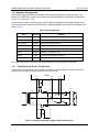
1.2 Hardware Assignments
The firmware supports two different hardware configurations for measuring a split-phase load. The
settings in the CESTATE register must correlate to the selected hardware configuration represented in
Section 1.2.1 and Section 1.2.2.
All measurement results, command routines, and configuration registers are accessible through the TX
and RX pins of serial 0 interface (UART0/RS232). Additional 78M6613 pins utilized by this firmware are
listed in Table 1.
Table 1: DIO Assignments
DIO#
Direction
Purpose
DIO6
Output
WPulse (SLIP and CLI)
DIO17
Output
Ready/Active (SLIP and CLI)
DIO7, DIO19
Output
Relay Control (SLIP and CLI)
DIO16
Output
SAG (SLIP and CLI)
DIO8/DIO4/DIO5
Input
RS485 Address (SLIP only)
DIO15
Output
RS485 Tx_Enable(SLIP only)
DIO14
Input
Invoke Boot Loader(SLIP and CLI)
DIO17
Output
Boot Loader Pulse(SLIP and CLI)
RTC (Real Time Clock), LCD Driver, and Battery Modes are not supported by this firmware.
1.2.1
Fixed Reference Sensor Configuration
In conventional configurations, the AC neutral is connected to V3P3A which is the supply input of the
analog circuitry and the reference potential for the A/D Converter.
A3
A1
78M6613
V3P3A
A0
A2
CT1
LOAD
IA
Line1
VA
Neutral
VB
Line2
IB
CT2
Figure 1: Simplified Connection Diagram with Fixed Reference
6
Rev. 2
UG_6613_090
1.2.2
78M6613 Split-Phase Firmware Description Document
Floating Reference Sensor Configuration
In order to maintain a high impedance between the supply (Line1, Line2, Neutral) and the measurement
subsystem, a “floating reference” configuration is also available.
(Vref)
A2
(Va)
A0
78M6613
V3P3A
A1
A3
V3P3_ REF
R
R
R1
R
R’
R’
I1
Neutral
V2
LOAD
R’
Line1
V1
R2
I2
Line2
Figure 2: Simplified Connection Diagram with Floating Reference
A virtual center or reference (V3P3_REF) has been created using a voltage divider (R1 and R2). The
V3P3A (AD/C reference potential) is connected to the virtual center. Two voltages are then acquired:
Line 1 and Neutral, these measurements are referred to the virtual ground (V3P3_REF). For clarity, Line
1 measurement is identified as Va and Neutral measurement is identified as Vref.
The equations to reconstruct the values of V1 and V2 are the following:
[1]
Rev. 2
7
78M6613 Split-Phase Firmware Description Document
UG_6613_090
Table 2 shows the results obtained from simulations using the above equations:
V1= Line 1 Voltage, V2= Line2 Voltage Vref (ADC input Neutral-V3P3_REF), Va (ADC input
Line1-V3P3REF). V1 and V2 are reconstructed as the resulting values from [1].
Table 2: Simulation Results
8
V1
V2
Vref
Va
V1
(reconstructed)
V2
(reconstructed)
120
120
0
120
120
120
100
120
9.768
109.768
100
120.0011429
80
120
19.535
99.535
80
120.0002381
60
120
29.303
89.303
60
120.001381
40
120
39.07
79.07
40
120.0004762
20
120
48.838
68.838
20
120.001619
0
120
58.605
58.605
0
120.0007143
V1
V2
Vref
Va
V1
(reconstructed)
V2
(reconstructed)
120
120
0
120
120
120
120
100
-9.768
110.232
120
99.99885714
120
80
-19.535
100.465
120
79.9997619
120
60
-29.303
90.697
120
59.99861905
120
40
-39.07
80.93
120
39.99952381
120
20
-48.838
71.162
120
19.99838095
120
0.5
-58.361
61.639
120
0.498904762
Rev. 2
UG_6613_090
1.3
78M6613 Split-Phase Firmware Description Document
Measurement Equations
The Split-Phase Library provides the user with continuously updated “Wideband” measurement data.
Wideband measurements are generally of interest when measuring in systems that tend to have
non-sinusoidal waveforms. Table 3 lists the basic measurement equations for the Wideband methods.
Table 3: Measurement Equations Definitions
Symbol
Parameter
Wideband Equation
V
RMS Voltage
V = √∑v(t)2
I
RMS Current
I = √∑i(t)
P
Active Power
P = ∑ (i(t) * v(t))
Q
Reactive Power
Q = √(S2 – P2)
S
Apparent Power
S=V*I
PF
Power Factor
P/S
PA
Phase Angle
ACOS (P/S)
2
The value of voltage and current are calculated as “true RMS”. The calculation requires an accumulation
of samples over time (accumulation interval), as follows:
Similarly for power:
[2]
Where n is the number of ADC samples in an accumulation interval for a given sample rate.
1.4
Sampling and Update Rates
This firmware utilizes an effective sampling rate of 3,641 samples per second for each sampled input.
While the CE continuously accumulates sampled data at the sampled rate, status and measurement data
updates to the MPU are less frequent. These updates include:
•
•
Sag status is updated at every Mux Chcle for low-latency alarm detection.
Measurement outputs and all other alarm conditions are updated every accumulation interval which is
set to 500msec for this firmware build.
Rev. 2
9
78M6613 Split-Phase Firmware Description Document
UG_6613_090
2 Functional Description
This section summarizes the functional operation of the 78M6613. Refer to the 78M6613 Data Sheet and
application notes for more information on IC operation and terminology.
2.1
Initialization and Start-up
Upon power-up, both MPU and Compute Engine (CE) cores start executing the application code from
designated blocks of Flash memory. Status indicators for ‘Ready’ and ‘Active’ are available to the host
via DIO pins.
2.2
Sensor (Hardware) Configuration
A few parameters specific to the hardware implementation may require one-time configuration. The
firmware allows for parameters to be modified by the user at run-time and saved to Flash. These
hardware-specific parameters include:
VMAX and IMAX registers define the upper and lower values of the ADC range. These parameters allow
the scaling of raw data to real-world values. VMAX and IMAX should be set to a value that reflects a
peak of near 250mV at the selected voltage ADC input. Values too far from this setting will cause
undesired effects. When changing a current sensor its associated IMAX value will need to be reevaluated.
The CESTATE register selects either the ‘Fixed’ or ‘Floating’ reference sensor configuration. Refer to
Section 1.2 for more information on sensor interface configurations.
2.3
AC Measurement and Monitoring
The integrated AFE and CE function as a data acquisition system, controlled by the MPU. The
low-voltage analog input signals are sampled and stored in CE DRAM where they are processed by the
CE. The CE, a dedicated 32-bit signal processor, performs the computations necessary to all the
measurements. The CE calculations and processes include:
•
Multiplication of each current sample with its associated voltage sample to obtain the energy per
sample (when multiplied with the constant sample time).
•
Frequency-insensitive delay cancellation on all channels (to compensate for the delay between
samples caused by the multiplexing scheme).
•
•
•
Monitoring of the input signal frequency (for frequency and phase information).
Monitoring of the input signal amplitude (for sag detection).
Scaling of the processed samples based on calibration coefficients.
At the end of each accumulation interval, these atomic measurement parameters are provided to the
MPU for post-processing. Alternate multiplexer cycles also gather measurements of the IC’s junction
temperature for additional compensation in the MPU. Post-processing functions handled by the MPU at
the end of every accumulation interval include:
•
•
•
•
Compensation for environmental variables.
Calculation of apparent power, power factor, phase angle, and line frequency.
Accumulation of energy data.
Comparing of measurement outputs to configurable alarm thresholds.
•
•
Scaling and formatting of output measurement data.
Updating of all output registers (data and alarm status).
10
Rev. 2
UG_6613_090
78M6613 Split-Phase Firmware Description Document
Figure 3 shows the data processing flow.
ADC
IA_RAW
PRECISION
REFERENCE
VA_RAW
SINC3
DECIMATOR
IA
VA
CROSSPOINT
IB
∆Σ
VB
X
X
X
X
X
X
X
CT
COMP
VB_RAW
DELAY
COMP
HPF
IA1
HPF
VA1
HPF
IB1
HPF
VB1
CAL_VA
IB_RAW
MODULATOR
+250mv
X
CAL_IA
CT
COMP
CAL_IB
FADC
DELAY
COMP
CAL_VB
TEMPERATURE
GAIN_ADJ
IA1
Σ
X
VA1
PLL
Σ
LPF
FREQ
QUANTA
(TMP)
Σ
X
F0
LINE FREQUENCY
VA_RAW
IB1
VB1
VCO OUT
Σ
LPF
QUANTB
WATTA
(TMP1)
WATTB
Σ
X
VAR 90
Σ
X
(TMP1)
IB1
IASQSUM
IBSQ
IBSQSUM
VBSQ
VB1
Σ
VABSQ
WATTASUM
WATTBSUM
WATT A
WATT A-B
WATTA-BSUM
WATT B
VARASUM
VAR A
VARBSUM
VAR B
QUANT_VARB
IASQ
VASQ
VA1
Σ
LPF
∑
X2
IA1
VARB
QUANT_VARA
(TMP)
VAR 90
VARA
Σ
LPF
÷N
∑
VASQSUM
VBSQSUM
VABSQSUM
÷N
√
Irms A
Irms B
Vrms A
Vrms B
Vrms A-B
Figure 3: Simplified Signal Processing Flow
Rev. 2
11
78M6613 Split-Phase Firmware Description Document
2.4
UG_6613_090
Configuration and Control
2.4.1
Input Registers
The following parameters are configurable by the user via input registers:
•
•
•
Sensor range and configuration
Calibration targets and coefficients
Squelch or CREEP Thresholds
•
Alarm Thresholds and Mask Settings
Updating Input Registers into Flash
The default values of all input registers can be updated by the user at run-time. A Flash update routine is
provided that saves the current value of any input register as the default.
2.4.2
Calibration
As with any measurement system, there are also multiple sets of compensation coefficients or
parameters that are used to compensate for system inaccuracies. Input registers for all coefficients can
be manually modified and saved to Flash. Alternatively, high level calibration routines can be invoked.
These routines automatically determine the coefficients for common parameters and save them to Flash
memory. The different types of compensation parameters include:
•
•
Voltage Sensing – Gain adjustment.
Current Sensing – Gain and offset (QUANT) adjustment.
•
Phase – Voltage-to-current phase offset compensation introduced by transformer or filters in sense
circuits.
•
•
•
Temperature – Offset for junction temperature at room temp.
Temperature – Coefficients for temperature curve.
WATT and VAR offset (QUANT) adjustment.
The calibration routines compensate for sensors and system inaccuracy. The new coefficients computed
during calibration are stored in the on-chip flash.
In order to perform a calibration, an external voltage source and external current source (or load) is
required. The calibration routines have a target voltage and current for both phases to match. The target
calibration voltage and current values are specified in the registers 0xC1 (Voltage Line1 and Line2) and
0xC2 (Current Line1 and Line2). Important factor for accurate calibration is to define the tolerance, for
example the coefficients are modified until the measured current or voltage is within the plus/minus range
of the specified tolerance from the target value. The voltage calibration tolerance register is at address
0xC4 while the current tolerance is specified in register 0xC5.
Other settings for calibration are average counts and maximum number of iterations.
The average counts represent the number of voltage measurement (register 0xC6) or current
measurements (register 0xC7) averaged and used to be compared against the target value.
The number of iterations sets the number of time the routine runs in order to bring the value of
either voltage or current reading within the specified tolerance from the target.
NOTE: All calibration should be done in the ‘Fixed Reference Sensor Configuration’.
12
Rev. 2
UG_6613_090
78M6613 Split-Phase Firmware Description Document
Figure 4 shows a split-phase calibration test setup.
UART
(HOST CONNECTION)
TX
78M6613
RX
A3
V3P3A
A1
A0
A2
CT1
IA
Line1
VA
PRECISION
AC VOLTAGE
SOURCE
PRECISION
AC LOAD
Neutral
VB
Line2
IB
CT2
Figure 4: Split-Phase Calibration Test Setup
The source and AC load should provide a stable reference during calibration. Since the calibration
procedures are dependent on production test setup, they will be described in a separate document.
Rev. 2
13
78M6613 Split-Phase Firmware Description Document
2.4.3
UG_6613_090
Relay Control
Relay control is supported by the TC command. The TC command can be used to open (0) or close (1)
circuit of all 2 channels. All necessary Sequence (time between each channel), Energized (for closing
circuit), and De-Energized (for opening circuit) delay times are set up and used by the library using the
following default values:
Energized delay time =
De-Energized delay time =
MPU
Parameter
Relay
Configuration
Energize
Delay
Location
(hex)
AC
AE
0ms
0ms
LSB
–
ms
Default
0
+0.000
De-Energize
Delay
AF
ms
+0.000
Control Relay
F0
–
0
14
Comment
Bit 1 (Relay Polarity)
0 = Normal Polarity
1 = Inverted Polarity
Bit 0 (Relay Type)
0 = non-latched
1 = latched
Parameter given in relay
manufacturer’s data sheet is
entered here. The amount of
delay will be 1 ms plus the value
entered in )AE.
Parameter given in relay
manufacturer’s data sheet is
entered here. The amount of
delay will be 1 ms plus the value
entered in )AF.
Bit 1 (Relay for Outlet 2)
0 = DIO19 = 0
1 = DIO19 =1
Bit 0 (Relay for Outlet 1)
0 = DIO7 = 0
1 = DIO7 = 1
Note: AC[1] = 1 inverts the bits
above.
Example
If the user desires 8 ms of
delay then enter the
following:
>)AE=+0.007<CR>
If the user desires 8 ms of
delay then enter the
following:
>)AF=+0.007<CR>
Control Relay
Rev. 2
UG_6613_090
78M6613 Split-Phase Firmware Description Document
2.4.3.1 TC Command
This section applies to the CLI version of the split-phase firmware. The SPI firmware controls the relays
directly using the F0 register described in Section 2.4.3.
Refer to the 78M6613 Split-Phase Evaluation Board User Manual for the specific hardware design. The
format of the TC command is as follows (where it is not a case sensitive):
>tc
is the same as >TC or >Tc or >tC.
>TCxx where xx is a hex value with each bit represents the setting of each channel. The value of each bit
is determined as 1 = closing and 0 = opening 0. Both channels will be processed sequentially starting
from the highest channel number first with a sequence delay time in between. It is important to note that if
the polarity for each Channel is inverted, bit 1 of the Relay Config register (0xF0) will be set accordingly in
order for the Relay Control to work properly.
The TC commands are summarized in the following table:
TCx
Relay Control Commands
Description
Allows the user to control the relay of all channels in one command.
Usage
TC1 or TC01
TC2 or TC02
TC3 or TC03
TC0 or TC00
Rev. 2
The TC command can be used to turn on/off
relay of both channels. Each bit represents
the control (1=on, 0=off) for each channel
where the LSB represents the lowest channel
number.
Examples:
Relay ON for Outlet 1, OFF all others.
Relay ON for Outlet 2, OFF all others.
Relay ON for both channels.
Relay OFF for both channels.
15
78M6613 Split-Phase Firmware Description Document
2.4.4
UG_6613_090
Sag Detection Settings
The 78M6613 Split-Phase Firmware includes the sag detection function. SAG is defined as a momentary
or permanent decrease of line voltage amplitude. The sag detection is often used to monitor the quality
of the power line or utilize the sag alarm to notify external devices (for example a host microprocessor) of
a pending power-down. The external device can then enter a power-down mode (for example saving
data or recording the event) before a power outage. Figure 5 shows a typical sag event.
SAG_THRESHOLD
SAG_COUNTER
Figure 5: Sag Event
The sag detection is base on a voltage threshold (SAG_THR), and a counter value (time). The counter is
updated at the ADC sample rate and starts whenever the voltage is below the SAG_THR value. The
alarm bit and alarm pin are set if the counter exceeds the predefined SAG_THR count (SAG_CNT) value.
SAG detection is enabled for VA or VB or both by setting bit 5 (VA) and/or bit 6 (VB) to logic high (1) in
the CE’s CESTATUS register (0x100E).
2.4.5
Creep Thresholds
The 78M6613 includes a “no-load” detection feature that eliminates what is commonly referred to as
“meter creep.” Meter creep is defined as power (or energy) that is read by the system when there is no
load attached. The FW sets line frequency, voltage and current to zero readings when the voltage falls
below a programmable threshold.
2.4.6
Limit Registers (Alarms)
The Limit registers set limits on result values and causes Status Register bits to be set when a limit
is exceeded. Limit registers use the same scaling applied to results, and as such, are user
definable.
The user selectable alarms are the following:
•
Min/Max Temperature Alarm.
•
Min/Max Frequency Alarm.
•
SAG Voltage Alarm.
•
Under-voltage (V1 input).
•
Over-voltage (V1 input).
•
Over-Current (Line 1 and Line 2).
•
Power Factor (Line 1 and Line 2).
•
Creep Alert low current alarm (Line 1 and Line 2).
16
Rev. 2
UG_6613_090
3
78M6613 Split-Phase Firmware Description Document
Split-Phase M-API Register Map
This section contains the register map for the Split-Phase M-API Library. All the registers are in a 4-byte
format and are divided in three sections:
•
•
•
Output Registers for reading metrology results, system status, etc.
Input Registers for entering commands, coefficients, etc.
CE (I/O) Registers for Compute Engine settings and status.
3.1
Output Registers
Output
Address
(hex)
Resolution
Data
Type
Description
Delta
Temperature
20
0.1 °C
Unsigned
Temperature difference from 22 °C.
Line Frequency
21
0.01 Hz
Unsigned
Line Frequency.
Bit 0 – Minimum Temperature Alarm.
Bit 1 – Maximum Temperature Alarm.
Bit 2 – Minimum Frequency Alarm.
Bit 3 – Maximum Frequency Alarm.
Bit 4 – SAG Voltage Alarm (Based on setting of CESTATUS register)
Bit 5 – LOPENB – Line open on Phase B.
Bit 6 – MAXV(A) – over maximum voltage on Phase A.
Bit 7 – LOPENA – Line open on Phase A.
Bit 8 – MAXIA– maximum current exceeded on Phase A.
Bit 9 – Reserved (0)
Bit 10 – Reserved (0)
Bit 11 – PFA min – Power Factor Min limit exceeded on Phase A.
Bit 12 – PFA Max – Power Factor Max limit exceeded on Phase A.
Alarm Status
22
Unsigned
Bit 13 – Reserved (0)
Bit 14 – MAXIB– maximum current exceeded on Phase B.
Bit 15 – Reserved (0)
Bit 16 – Reserved (0)
Bit 17 – PFB min – Power Factor Min limit exceeded on Phase B.
Bit 18 – PFB Max – Factor Max limit exceeded on Phase B.
Bit 19 – Multi-Fault (When Vrms(total) < Vmin * 2 (Vmin = register
0xD5)
Bit 20– MAXIT – Total current(Phase A and B) Max limit exceeded
Bit 21 – CREEP A Alert – current Creep Alert on Phase A
Bit 22 – CREEP B Alert – current Creep Alert on Phase B.
Bit 23 – FAULT – Line/Neutral reversed.
Bit 24-25 – Reserved (0)
Bit 26 – CE_READY – CE is now ready after power up.
Bit 27 – 31 – Reserved (0)
Not Used
23-25
–
–
Not Used
Vrms A
26
1/000 Vrms
Unsigned
RMS Voltage Phase A
Watts A
27
1/1000 Watt
Signed
Power Phase A
Wh A (Export)
28
1/1000 WattHr
Unsigned
Energy Phase A (Export)
Wh A (Import)
29
1/1000 WattHr
Unsigned
Energy Phase A (Import)
Irms A
2A
1/1000 Arms
Unsigned
RMS Current measurement Phase A
VAR A
2B
1/1000 Watt
Signed
Reactive Power measurement Phase A.
VA A
2C
1/1000 Watt
Signed
Apparent power measurement Phase A
Rev. 2
17
78M6613 Split-Phase Firmware Description Document
UG_6613_090
Output
Address
(hex)
Resolution
Data
Type
Power Factor A
2D
0.001
Signed
*Phase A Power Factor. The output will be between -0.950 and 1.000.
Phase Angle A
2E
0.001°
(degrees)
Signed
Phase A phase angle. The output will be between 180.000 and
-180.000.
Wh A (Net)
2F
1/1000 WattHr
Unsigned
Energy Phase A (Net) Balance
Vrms B
66
1/1000 Vrms
Unsigned
RMS voltage Phase B
Watts B
67
1/1000 Watt
Signed
Power Phase B
Wh B (Export)
68
1/1000 WattHr
Unsigned
Energy Phase B (Export)
Description
Wh B (Import)
69
1/1000 WattHr
Unsigned
Energy Phase B (Import)
Irms B
6A
1/1000 Arms
Unsigned
RMS Current measurement Phase B
VAR B
6B
1/1000W
Signed
Reactive power measurement Phase B
VA B
6C
1/1000 W
Signed
Apparent power measurement Phase B
Power Factor B
6D
0.001
Signed
*Phase B Power Factor. The output will be between -0.950 and 1.000.
Phase Angle B
6E
0.001°
(degrees)
Signed
Phase B phase angle. The output will be between 180.000 and
-180.000.
Wh B (Net)
6F
1/1000 WattHr
Unsigned
Energy Phase B (Net)
Watts Total
90
1/1000 Watt
Signed
Power Total (Phase A and B)
Wh Total (Export)
91
1/1000 WattHr
Unsigned
Energy Total (Export)
Wh Total (Import)
92
1/1000 WattHr
Unsigned
Energy Total (Import)
Irms Total
93
1/1000 Arms
Unsigned
RMS Current measurement Total (Phase A and B)
VAR Total
94
1/1000W
Signed
Reactive power measurement Total (Phase A and B)
VA Total
95
1/1000 W
Signed
Apparent power measurement Total (Phase A and B)
Wh Total (Net)
96
1/1000 WattHr
Unsigned
Energy Total (Net)
Vrms(A-B)
97
1/1000 Vrms
Unsigned
RMS Voltage (A -B)
* Positive power factor is defined as current lagging voltage (inductive). Negative power factor is defined
as voltage lagging current (capacitive).
18
Rev. 2
UG_6613_090
3.2
78M6613 Split-Phase Firmware Description Document
Input Registers
MPU Parameter
Location
LSB
(hex)
Default
Comment
VMAX
A0
1/000 Vrms
471500
External RMS voltage corresponding to 250 mVpk (Max
ADC range). VMAX Calculation:
ICREEP A
A1
1/1000 Arms
7
Minimum RMS current to be reported for Phase A.
Currents measured below this value will be ignored.
IMAX A
A2
1/1000 Arms
52000
External RMS voltage corresponding to +/-250 mVpk (Max
ADC range).
IMAX Calculation: IMAX= (250mV/√2)/Rshunt
ICREEP B
A3
1/1000 Arms
7
Minimum RMS current to be reported for Phase B.
Currents measured below this value will be ignored.
IMAX B
A4
1/1000 Arms
52000
External RMS voltage corresponding to +/-250 mVpk (Max
ADC range).
IMAX Calculation: IMAX= (250mV/√2)/Rshunt
Unused
A5
–
–
Unused
NOM_TEMP
A6
–
0
Temp_raw_x reading at 22 °C. Needed to enable
temperature compensation.
Reserved
A7-BC
–
–
Reserved
VMAX = (250mV/√2)/(Rshunt/( Rseries - Rshunt))
This register is 1-byte size and is used for controlling the
Min/Max and accumulation data as follows when the bit is
set:
BIT0 – WPulse goes into DIO6
BIT1 – Reserved
Config
BD
–
1
BIT2 – Reserved
BIT3 – Start Min/Max
BIT4 – Restart Min/Maz
BIT5 – Allow Negative Power Factor
BIT6 – Clear Counts
BIT7 – Clear Accumulation data (Wh).
Rev. 2
19
78M6613 Split-Phase Firmware Description Document
MPU Parameter
Location
LSB
(hex)
Default
UG_6613_090
Comment
This register is used for calibration Status
Calibration Status:
Bit =0 (clear) Calibration OK ,
Bit =1 (set) Calibration Failed
BIT0 – Temperature Cal/Status
BIT1 – Voltage CAL A Status
BIT2 – Voltage CAL B Status
Calibration Status
BE
–
0
BIT3 – Phase CAL A Status
BIT4 – Phase CAL B Status
BIT5 – Current CAL A Status
BIT6 – Current CAL B Status
BIT7 – Watt CAL A Status
BIT8 – Watt Cal B Status
BIT9-29 – Reserved
BIT30 – UPDATE_FLASH_MPU Status
BIT31 – UPDATE_FLASH_CE Status
Tolerance on Phase
BF
0.001°
100
Measured value to fall within this set tolerance plus/minus
the target value (Calibration Phase entry) for the calibration
to be complete.
Reserved
C0
–
0
Reserved
Calibration Voltage
C1
1/000 Vrms
120000
Target line voltage (rms) used for calibration on both
Phase A and Phase B.
Calibration Current
C2
1/1000 Arms
1000
Target load current (rms) used for calibration on both
Phase A and Phase B.
Calibration Phase
C3
0.1°
0
Target Phase (voltage to current). Normally set to zero.
For both Phase A and Phase B.
Tolerance on Voltage
C4
1/000 Vrms
10
Measured value to fall within this set tolerance of the target
value (Calibration Voltage entry) for the calibration to be
complete.
Tolerance on Current
C5
1/1000 Arms
10
Measured value to fall within this set tolerance plus/minus
the target value (Calibration Current entry) for the
calibration to be complete.
Average Count for
Voltage
C6
1
3
Number of voltage measurements taken and averaged to
be compared to the target value (Calibration Voltage
entry).
Average Count for
Current
C7
1
3
Number of current measurements taken and averaged to
be compared to the target value (Calibration Current
entry).
Max Iteration for
Voltage
C8
1
10
Number of attempts to reach the target value (Calibration
Voltage entry) within the programmed tolerance.
Max Iteration for
Current
C9
1
10
Number of attempts to reach the target value (Calibration
Current entry) within the programmed tolerance.
Tolerance on Watts
CA
1/1000 Watt
10
Measured value to fall within this set plus/minus tolerance
of the target Watt value for the calibration to be complete.
20
Rev. 2
UG_6613_090
78M6613 Split-Phase Firmware Description Document
MPU Parameter
Location
LSB
(hex)
Default
Comment
Average Count for
Watts
CB
1
3
Measured value to fall within this set tolerance plus/minus
the target Watt value for the calibration to be complete.
Max Iteration for Watts
CC
1
10
Number of attempts to reach the target value within the
programmed tolerance.
Reserved
CD
Calibration
Temperature
CE
0.1°C
220
Target nominal temperature for calibration.
Calibration Watts
CF
1/1000 Watt
120000
Target Watts used for calibration for both Phase A and
Phase B.
Temp Alarm Min
Threshold
D0
0.1°C
0
Minimum Temperature Alarm Threshold. A temperature
below this threshold will set the alarm (bit 0 of the Alarm
Status Register).
Temp Alarm Max
Threshold
D1
0.1°C
7000
Maximum Temperature Alarm Threshold. A temperature
above this threshold will set the alarm (bit 1 of the Alarm
Status Register).
Frequency Minimum
Threshold
D2
0.01Hz
5900
Minimum Frequency Alarm Threshold. A frequency below
this threshold will set the alarm (bit 2 of the Alarm Status
Register).
Frequency Maximum
Threshold
D3
0.01Hz
6100
Maximum Frequency Alarm Threshold. A frequency above
this threshold will set the alarm (bit 3 of the Alarm Status
Register).
SAG Voltage Alarm
Threshold
D4
1/000 Vpk
80000
Sets an alarm (bit 4 of the Alarm Status Register) if voltage
drops below the SAG threshold (and CESTATUS register
bit5 or/and bit6 are set)
Min Voltage Alarm
Threshold
D5
1/000 Vrms
100000
Minimum voltage level selected to flag user (bit 19 of the
Alarm Status Register).
Peak Voltage Alarm
Threshold
D6
1/000 Vrms
140000
Peak voltage setting that user wishes to flag (bit 6 of the
Alarm Status Register).
Unused
D7-D8
–
PFA_ Neg Threshold
DC
–
-700
Wideband Power Factor Negative Threshold. A less
negative wideband power factor than this threshold will set
an alarm (bit 11 of the Alarm Status Register). Only
available if register 0xF2 bit 2 is set to 1.
PFA_ Pos Threshold
DD
–
700
Wideband Power Factor Positive Threshold. A positive
wideband power factor less than this threshold will set an
alarm (bit 12 of the Alarm Status Register).
Unused
DE - DF
–
–
Unused
Unused
E0 - E5
–
–
Unused
Alarm Mask_Status
E6
–
0x04FFFFFF
Alarm mask for bits in the Alarm Status register. A “0”
masks the alarm from the register bit.
Alarm Mask_Alarm
E7
–
0x04FFFFFF
Alarm mask for an alarm pin (if DIO is configured). A “0”
masks the alarm (no report).
Rev. 2
21
78M6613 Split-Phase Firmware Description Document
3.3
UG_6613_090
CE Parameters
The following table lists the CE parameters for the firmware. With the exception of CESTATE and
QUANT registers, the user does not typically need to alter any of these input registers as they are
automatically set by Calibration Commands.
CE Parameter
Locatio
n (hex)
LSB
Default
Comment
CAL IA
1008
16384 is the default and is a gain of 1.
32767 is max giving a gain of 2.
16384
Gain constant for Phase A input.
CAL IB
1009
16384 is the default and is a gain of 1.
32767 is max giving a gain of 2.
16384
Gain constant for Phase B input.
CAL VA
100A
16384 is the default and is a gain of 1.
32767 is max giving a gain of 2.
16384
Gain constant for Phase A input.
CAL VB
100B
16384 is the default and is a gain of 1.
32767 is max giving a gain of 2.
16384
Gain constant for Phase B input.
PHASE_ADJ_IA
100C
-16384 ≤ PHASE_ADJ_IA ≤ +16384
0
Line Out A Phase adjustment =15
-14
* PHASE_ADJ_IA * 2 (degrees)
PHASE_ADJ_IB
100D
-16384 ≤ PHASE_ADJ_IB ≤ +16384
0
Line Out B Phase adjustment =15
-14
* PHASE_ADJ_IB * 2 (degrees)
CESTATE
100E
n/a
5061
Bit 15-8
SAG_CNT. Number of
consecutive voltage
samples below SAG
Threshold to assert
SAG alarm
Bit 7
Reserved (1)
Bit 6
1 = detect SAG on V1/B
Bit 5
1 = detect SAG on V0/A
Bit 2
1 = Floating Reference
0 = Fixed Reference
Bit 1-0
Kh = VMAX A * IMAX A / (WRATE * X)
WRATE
100F
Reserved
1010
SAG Threshold
1011
VMAX * 4.2551E-07 (Vpk)
QUANTA
1012
VMAX A * IMAX A * 1.8541E-10
(Watt)
1013
VMAX A * IMAX B * 1.8541E-10
(Watt)
1014
VMAX A * IMAX A * 1.8541E-10
(Watt)
QUANTB
QUANT VAR A
22
1.6826E+01 WattSec
+ 20732
Reserved (0)
Controls the number of pulses that
are generated per measured Wh
and VARh measurements.
Reserved
+168225
The voltage threshold for SAG
warnings. (80vRMS when
VMAX=471.5v) V0 must be above
this to prevent SAG alarm.
0
Compensation added to the Watt
calculation for Phase A. Used for
compensation at low current
levels. Keep below 10000d.
0
Compensation added to the Watt
calculation for Phase B. Used for
compensation at low current
levels. Keep below 10000d.
0
Compensation added to the VAR
calculation for Phase A. Used for
compensation at low current
levels. Keep below 10000d.
Rev. 2
UG_6613_090
78M6613 Split-Phase Firmware Description Document
CE Parameter
Locatio
n (hex)
LSB
Default
Comment
QUANT VAR B
1015
VMAX A * IMAX B * 1.8541E-10
(Watt)
0
Compensation added to the VAR
calculation for Phase B. Used for
compensation at low current
levels. Keep below 10000d.
0
Phase A input compensation
added for input noise and
truncation in the squaring
2
calculation for I . Used for
compensation at low current
levels. Keep below 10000d.
QUANT IA
1016
2
2
(IMAX A) * 4.6351E-11 (A )
QUANT IB
1017
(IMAX B) * 4.6351E-11 (A )
0
Phase B input compensation
added for input noise and
truncation in the squaring
2
calculation for I . Used for
compensation at low current
levels. Keep below 10000d.
Reserved
1018
–
–
Reserved
Temperature Gain
Adjust
1019
16384 is the default and is a gain of 1.
+16384
32767 is the max giving a gain of
2.
VREF_CORR
101A
–
0
Vref correction.
Rimbalance_CORR
101C
–
0
Resistor Imbalance correction
Rev. 2
2
2
23
78M6613 Split-Phase Firmware Description Document
4
UG_6613_090
Serial Communication
The serial communication with the 78M6613 takes place over a UART (UART0) interface. The default
settings for the UART of the 78M6613, as implemented in this firmware, are given below:
Baud Rate:
Data Bits:
Parity:
Stop Bits:
Flow Control:
38400bps
8
None
1
None
The host’s serial interface port is required to implement these settings on its UART. In addition, the
78M6613 Split-Phase Firmware is available with one of two protocols. The two available protocols are
briefly summarized below and fully documented in the Appendices.
4.1
CLI Firmware Application
The Command Line Interface (CLI) provides a simple ASCII interface to access input and output registers
and to invoke commands. The CLI interface connects to a HyperTerminal or any other terminal emulation
SW. The CLI interface can also be used to interface to a host processor. Appendix A describes the CLI
commands and syntax.
4.2
SLIP Firmware Application
The Serial Line Interface Protocol is a simple binary UART protocol defined to support single (e. g.
RS232) or multi-point device (e. g. RS485) interfaces. Appendix B describes the SLIP protocol and
command/response format of the data packet.
5
Contact Information
For more information about Maxim products or to check the availability of the 78M6613, contact technical
support at www.maxim-ic.com/support.
24
Rev. 2
UG_6613_090
78M6613 Split-Phase Firmware Description Document
Appendix A – Command Line Interface
This appendix describes a serial interface protocol called Command Line Interface (CLI). This interface
facilitates communication via UART between the energy measurement device and the host system by
use of ASCII-based commands and responses.
The characters following the command prompt symbol “>” are the CLI command characters. A
following carriage return “<CR>” is used to initiate the commands.
A.1 Identification Command
The I command is used to identify the revisions of Demo Code and the contained CE code. The host
sends the I command to the 78M6613 as follows:
>I<CR>
The 78M6613 will reply to the host the following:
V1.00 2s F0 W 78M6613 Split Phase 3+S2,Aug 16 2011
>
A.2 Reset Commands
A soft reset of the device can be performed by using the Z command. The soft reset restarts code
execution at addr 0000 but does not alter XRAM contents. The soft reset also sets all the registers to
their default values. To issue a soft reset to the device, the host sends the following:
>Z<CR>
The W command acts like a hardware reset. The energy accumulators in XRAM will reset back to zero.
Z
Reset
Description:
Allows the user to cause soft resets.
Usage:
Z
Soft reset.
W
Simulates watchdog reset.
Rev. 2
25
78M6613 Split-Phase Firmware Description Document
UG_6613_090
A.3 Data Access Commands
All the measurement calculations are stored in the data range of the device. The host requests
measurement information using the data access command which is a right parenthesis
>) addr <CR>
To request information, the host sends the data access command, the address (in hex) which is
requested, the format in which the data is desired (Hex or Decimal) and a carriage return. The contents
of the addresses that would be requested by the host are contained in Register Map.
A.3.1 Individual Address Read
The host can request the information in hex or decimal format. In an address read command, the
character $ requests the information to be returned in hex format. While the character ?, requests
information to be returned in decimal. When requesting information in decimal, the data is preceded by a
+ or a -.
An example of a command requesting the measured output located at address 0x28 in decimal is as
follows:
>)28?<CR>
An example of a command requesting the measured output located at address 0x28 in hex is as follows:
>)28$<CR>
A.3.2 Consecutive Read
The host can request information from consecutive addresses by adding additional ? for decimal or
additional $ for hex.
An example of requests for the contents in decimal of ten consecutive addresses starting with 0x32 is:
>)32??????????<CR>
An example of requests for the contents in hex of ten consecutive addresses starting with 0x32 would be:
>)32$$$$$$$$$$<CR>
Note: The number of characters per line is limited to no more than 60.
A.3.3 Block Reads
The block read command can also be used to read consecutive registers.
For decimal format:
> )startaddress:endaddress?
For hexadecimal format:
> )startaddress:endaddress$
The following block read command requests a block of measurement information in decimal format:
>)20:3D?<CR>
26
Rev. 2
UG_6613_090
78M6613 Split-Phase Firmware Description Document
A.3.4 Concatenated Reads
Multiple commands can also be added on a single line. Requesting information in decimal from two
locations and the block command from above are given below:
>)32?)35?)20:2E?<CR>
Note: The number of characters per line is limited to no more than 60.
A.3.5 Repeat Command
The repeat command can be useful for monitoring measurements and is efficient in demands from the
host.
If the host requests the contents of eight consecutive addresses with the following command string:
>)21????????<CR>
If the host then desires this same request without issuing another command, the repeat command can be
used:
>, (no carriage return needed for the repeat command)
The host only needs to send one character rather than an entire string.
Auxiliary
Description:
Various
Commands:
,
Typing a comma (“,”) repeats the command
issued from the previous command line. This is
very helpful when examining the value at a
certain address over time, such as the CE
DRAM address for the temperature.
/
The slash (“/”) is useful to separate comments
from commands when sending macro text files
via the serial interface. All characters in a line
after the slash are ignored.
Rev. 2
27
78M6613 Split-Phase Firmware Description Document
UG_6613_090
A.3.6 CE Data Access
The CE is the main signal processing unit in the device. The commands are similar to the MPU access
except that the host requests access to information from the CE data space using the CE data access
command which is a right bracket:
>]
Single Register CE Access
An example of a command requesting the contents located at CE address 0x28 in decimal is as follows:
>]28?<CR>
An example of a command requesting the contents located at address 0x28 in hex is as follows:
>]28$<CR>
Consecutive CE Reads
The host can request information form consecutive addresses by adding additional ? for decimal or
additional $ for hex.
An example of requests for the contents in decimal of ten consecutive addresses starting with 0x28 would be:
>]28??????????<CR>
An example of requests for the contents in hex of ten consecutive addresses starting with 0x28 would be:
>]28$$$$$$$$$$<CR>
Note: The number of characters per line is limited to no more than 60.
28
Rev. 2
UG_6613_090
78M6613 Split-Phase Firmware Description Document
A.4 Write Commands
A.4.1 MPU Register Write Commands
To modify the contents of an individual MPU Input Register, append the = character and the value to a
read command.
>)addr=n<CR>
The )U command is used for updating default values of the MPU input registers permanently in the flash.
Before issuing the )U command, CE must first be turned off by the disable CE command.
>CE0<CR>
>)U<CR>
>CE1<CR>
A.4.2 CE Register Write Commands
To modify the contents of an individual MPU Input Register, append the = character and the value to a
read command.
>]addr=n<CR>
The ]U command is used for updating default values of the CE input registers permanently in the flash.
Before issuing the ]U command, CE must first be turned off by the disable CE command.
>CE0<CR>
>]U<CR>
>CE1<CR>
A.5 Calibration Commands
There are often two types of built-in calibration routines. The first type provides complete calibration. The
second group, called atomic calibration commands, provides calibration for individual portions of the IC.
There is often one calibration coefficient for each voltage input and one for each current input.
A.5.1 Complete Calibration Command
The CAL command provides single-command calibration. To use this command, a precision voltage
source and a precision current source are required
Enter the following:
>CAL<CR>
The response is:
TCal OK
VCal OK
ICal 0 OK
>
The device calibrates the temperature (and saves to flash), calibrates the voltage (and saves them to
flash), and finally calibrates the current (and saves to flash).
Rev. 2
29
78M6613 Split-Phase Firmware Description Document
UG_6613_090
A.5.2 Atomic Calibration Commands
The atomic calibration commands provide individual calibration of voltage, current, power, and
temperature. A sequence of these commands results in a fully calibrated unit. The following table
provides a summary of the atomic calibration commands.
CLxx
Atomic Calibration
Commands
Description:
Allows the user to Calibrate individual sections of the IC.
Usage:
CLV
Calibrates voltage only.
CLI1
Calibrate current only.
CLT
Calibrate temperature only.
CLV Command
An example of an atomic calibration command would be to calibrate voltage with the CLV command. The
CLV command calibrates voltage to the target value and tolerance and saves the coefficients to flash.
The CLV command example is given below:
>CLV<CR>
The response is:
VCal OK
>
CLI Command
The user can then calibrate the current using the CLI command. The CLI1 command calibrates the
current channel 1 to the target value and tolerance and saves the coefficients to flash. The CLI1
command example is given below:
>CLI1<CR>
The response is:
ICal 0 OK
>
CLT Command
The CLT command is used for the temperature calibration. With this command, the CE register holding
current temperature are read and entered into MPU register C0 and the contents are then saved to flash.
The CLT command example is given below:
>CLT<CR>
The response is:
TCal OK
>
30
Rev. 2
UG_6613_090
78M6613 Split-Phase Firmware Description Document
Appendix B – SLIP Interface
This appendix describes a multi-point serial interface protocol built on top of a Serial Line Interface
Protocol (SLIP) layer. It defines a payload format suitable for communicating with one or more 78M66xx
energy measurement devices on a single serial bus.
B.1 Packet Format and Definition
The SLIP packet is transmitted in a block format. The useful data is encapsulated by two control bytes.
These control bytes are necessary to determine when the block starts and ends. It is recommended that
the host allows the firmware sufficient time to process each byte of the packet by setting a 5ms intercharacter delay.
B.1.1 Packet Format
Start
Device Address
Data
CRC-8
End
“C0”
XX
XX… XXn
XX
“C0”
1Byte
1Byte
Variable, nBytes
1Byte
1Byte
Offset = 0
Offset = 1
Offset = 2
Offset = n+2
Offset = n+3
B.1.2 Start and End
A SLIP packet always starts and ends with an END character. SLIP has 4 special character codes:
#define END 0xC0
#define ESC 0xDB
#define ESC_END 0xDC
#define ESC_ESC 0xDD
/* Decimal 192 - indicates start or end of a packet */
/* Decimal 219 - indicates byte stuffing */
/* Decimal 220 - ESC ESC_END means END data byte */
/* Decimal 221 - ESC ESC_ESC means ESC data byte */
Within a SLIP packet, a data byte having a value of END (0xC0) will be stuffed with ESC (0xDB) and
immediately followed by an ESC_END (0xDC) character, for example: 0xC0 data byte will appear as
0xDBDC.
Similarly, a data byte having a value of ESC (0xDB) will be immediately followed by an ESC_ESC (0xDD)
character, for example: 0xDB data byte will appear as 0xDBDD.
B.1.3 Device Address
The SLIP-based interface supports a single master and multi-slave devices configuration. Messages are
broadcasted on the bus by the master. The device address is contained in the message packet, so that
only the specific device responds to the broadcast request. Since the device cannot detect presence of
other devices on the network, it is the task of the host to manage the device addresses from the initial
response to make sure no two devices with the same address are present as collision will occur.
One byte device address, ranging from 0x00 - 0x7F, shall be assigned to each 78M66xx device. Device
address for each 78M66xx device shall be hardcoded using the DIO lines, for example: device addresses
in the range of 0x00 to 0x07 can be assigned by using three input DIO lines.
The response packet shall be embedded with the responding device’s address to identify the source of
the packet and other devices shall ignore the response packet.
The packet transaction is always a command/response pair such that the master will initiate the
communication by sending a request packet to a device with an assigned address. Only the addressed
device will respond to the master by a NACK in the case of a bad packet, or an ACK followed by a
response packet in the case of a good packet, to complete the transaction.
Rev. 2
31
78M6613 Split-Phase Firmware Description Document
UG_6613_090
B.1.4 Data
The data packet consists of either the request data sent from the master to the device or the response
data packet sent from the device to the master. If a data byte is 0xC0, it is replaced by 0xDBDC. If it is
0xDB, it is replaced with 0xDBDD. The conversion is done before transmission. See sample code below.
B.1.5 CRC-8
An 8-bit cyclic redundancy check (CRC-8) calculated over the Data packet is embedded in the packet.
8
2
The CRC-8 represented by the polynomial, C(x) = x + x + x + 1.
After the computation of CRC, Data packet and CRC-8 is encoded with the special SLIP character codes
described in Section 2.2.
Start
Device Address
Data
CRC-8
End
“C0”
XX
XX… XXn
XX
“C0”
1Byte
1Byte
Variable, nBytes
1Byte
1Byte
Offset = 0
Offset = 1
Offset = 2
Offset = n+2
Offset = n+3
SLIP character codes
Code snippet for CRC-8 calculation:
uint8_t crc8( uint8_t inCrc, uint8_t inData )
{
uint8_t i,crc;
crc = inCrc ^ inData;
for ( i = 0; i < 8; i++ )
{
if (( crc & 0x80 ) != 0 )
{
crc <<= 1;
crc ^= 0x07;
}
else
crc <<= 1;
}
return crc;
}
B.2 Packet Types
The master shall broadcast a command packet addressed to a specific device. And the device shall reply
by transmitting an ACK/NACK packet followed by a response packet.
The different packet types can be classified as.
•
•
•
ACK/NACK Packet – Handshake mechanism.
Command Packet – Operational phase.
Response Packet – Reply to the command.
After sending the command packet, the master must wait for a response from the device before sending
out the next command packet. In the case of a non-responsive device, a time-out shall be activated by
the master before re-sending the command packet to the device.
32
Rev. 2
UG_6613_090
78M6613 Split-Phase Firmware Description Document
ACK/NACK Packet
Every time a request packet is sent from the master to the device, the master should expect an
ACK/NACK packet back from the device. ACK is to acknowledge the valid address and data integrity of
the request packet.
NACK acknowledges the data integrity error like CRC error. Only device with valid address should
respond with a NACK packet to avoid message collision on the bus. After sending out the NACK packet,
the device considers the transaction to be complete. The device will be in receive mode, ready to receive
a new command packet from the master.
If NACK is received, from the device, the master shall be in transmit mode and resend the command.
The number of retries shall be at the discretion of the master. The device shall consider each retry
attempt as a new command request from the master.
Start
Device Address
Data
CRC8
End
“C0”
XX (responding
device address)
ACK/NACK
XX
“C0”
1Byte
1Byte
1 Byte
1 Byte
1 Byte
Offset = 0
Offset = 1
Offset = 2
Offset = 3
Offset = 4
The table below describes in detail each field of the ACK/NACK packet and its available values.
ACK/NACK packet sent from the device
Packet
Offset
2
Packet Names
ACK/NACK
Field Value
Field Size
XX
1 byte
Field Description
ACK
: 0x00.
NACK* : 0x80
*NACK for the checksum error.
Command Packet
The command packet is sent from the master to the device. Upon reception of the command packet, the
device sends an ACK packet to the master to inform the master that it has successfully received the
command and is working on it. After processing of the command, the device responds to the master with
the response packet.
The operational phase comprises of the register read/write and device information command.
The 661x device register address is two bytes wide and register data is four bytes wide. Refer to 661x
Firmware Description Document(FDD) for the register details. The following table shows the offset of the
MPU, CE and IO RAM registers.
Register
Offset
MPU
0x0000
CE
0x1000
IO RAM
0x2000
For example, an offset of 0x1000 is added to the CE register addresses defined in the Firmware
Description Document.
Rev. 2
33
78M6613 Split-Phase Firmware Description Document
UG_6613_090
The read/write command is limited to sixteen registers read/write operation due to the receive and
transmit buffer size limitation of the device.
The device may take up to a few seconds to complete the calibration command (a MPU register – see
FDD for details). Therefore the master shall allow the device enough time to process a command and wait
for the device response packet before timing out or sending a new command to the device.
During Operational phase, after receiving the valid start character and device address, the device shall
start a timer of 250ms. If this timer expires before receiving the end character, the receive buffer of the
device is flushed and the device is ready to receive the new command packet. If the end character is
received prior to expiration of this timer, the timer will be stopped and reset.
The communication flow is depicted as follows:
Master
Device
Command
Packet
ACK
Response
Packet
Start
Device Address
Data
CRC-8
End
“C0”
XX
XX… XXn
XX
“C0”
1Byte
Variable,
n Bytes
1 Byte
1Byte
Offset = 1
Offset = 2
Offset = n+3
Offset = n+4
1Byte
Offset = 0
34
Command Type
Command Request Data
XX
XX
1Byte
n Bytes
Offset = 2
Offset = 3
Rev. 2
UG_6613_090
78M6613 Split-Phase Firmware Description Document
The following table describes in detail each field name and its available values:
Command Packet Sent from the master to the device.
Packe
t
Offset
Packet
Names
Command
Field Value
Field
Size
Packet Description
2
CmdType
Variable
1 byte
Read(single or multiple)
Write(single or multiple)
Contiguous Block Read
Contiguous Block Write
Device Information
CLI Toggle Cmd
: 0x10
: 0x11
: 0x20
: 0x21
: 0x30
: 0x00
3
CmdRequest
Data
Variable
n bytes Single/Multiple Read:
<Register address> , <Register address2>
Single/Multiple Write:
<Register address1> <data1> , <Register address2>
<data2>, ….
Contiguous Block Read:
<Beginning block read register address, <number of
registers to read>
Contiguous Block Write:
<Beginning block write register address> <data1>,
<data2>,<data3>….
Device Information:
<none>
CLI Toggle Command:
<none>
The following table describes the field size of each data packet:
Data Packet
Field Size
<Register address>
2 bytes
<Data>
4 bytes
<Beginning block read/write register address>
2 bytes
<number of registers to read>
1 byte
Rev. 2
35
78M6613 Split-Phase Firmware Description Document
UG_6613_090
Response Packet
The Response packet is sent from the device to the master in reply to the Command packet.
Start
Device Address
“C0”
1Byte
Offset = 0
XX (responding
device address)
1Byte
Offset = 1
Data
CRC-8
End
XX… XXn
XX
“C0”
Variable, nBytes
Offset = 2
1 Byte
Offset = n+5
1 Byte
Offset = n+6
Cmd Read/Write Status
Cmd Return Code
Command Response Data*
XX
2 Bytes
Offset = 2
XX
1Byte
Offset = 4
XX
n Bytes
Offset = 5
* only for read operation.
The table below describes in detail each field name and its available values.
Response Packet Sent from the Device
Packet
Offset
2
Packet Names
CmdRWStatus
Command
Field Value
Variable
Field
Size
Packet Description
2 bytes Each bit represents status of the register read/write
operation.
Bit = 0 – Success.
Bit = 1 – Failure.
LSB represents first read/write register operation in
the command. The maximum number of register
addresses for both read/write operations in a
command is limited to 8.
CmdRWStatus is not applicable to Device
Information command.
4
CmdReturnCode
variable
1 byte
Successful operation
Invalid Command Type
Incorrect Data Length
Read-only register
Reserved register
Invalid register address
5
CmdResponseData
variable
n bytes Single/Multiple Read:
<data1> <data2> …….<data n>
: 0x00
: 0x80
: 0x81
: 0x82
: 0x83
: 0x84
Single/Multiple Write:
<none>
Contiguous Block Read:
<data1> <data2> …….<data n>
Contiguous Block Write:
<none>
Device Information:
ASCII string depicting the firmware version and the
product number.
CLI Toggle Command:
<none>
36
Rev. 2
UG_6613_090
78M6613 Split-Phase Firmware Description Document
Example 1 – Read Command Packet
In this example, the master sends a command request to read MPU register address 0x0200 of the 661x
device (with device address 0x07). The device accepts the read command by sending out an ACK
followed by the register data, i.e., 0x000731CC. The next example is when the command packet
attempts to read an invalid register address.
For a successful transaction:
C0 07 10 02 00 88 C0
register 0x0200
C0 07 00 00 C0
C0 07 00 00 00 00 07 31 CC 90 C0
For a failed transaction:
C0 07 10 03 10 ED C0
register 0x0310
C0 07 00 00 C0
C0 07 00 01 84 00 00 00 00 31 C0
// Master sends read command Request Packet to read MPU
// Device sends ACK
// Device sends out register data – 0x000731CC
// Master sends read command Request Packet to read MPU
// Device sends ACK. Packet receipt successfully.
// Device sends out an error code of 0x84
Example 2 – Write Command Packet
In this example, the master sends a command request to write data 0x000927C0 to the MPU register
address 0x0200 of the device (with device address 0x07). The device accepts the write command by
sending out an ACK followed by a command response packet after successfully completing the write
command.
C0 07 11 02 00 00 09 27 DB DC EF C0 // Master sends command request packet to write to the
register addr 0x0200
C0 07 00 00 C0
// Device sends ACK
C0 07 00 00 00 00 C0
// Device sends out command response packet after
successful write.
Example 3 – Contiguous Block Read Command Packet
In this example, the master sends a command request to read three contiguous MPU registers from
starting address 0x0200 of the 661x device ( with device address 0x07). The device accepts the block
read command by sending out an ACK followed by the register data. The next example is when the
command packet attempts to read an invalid MPU register address.
C0 07 20 02 00 03 xx C0
// Master sends block read command
request
C0 07 00 00 C0
// Device sends ACK
C0 07 00 00 00 00 09 27 DB DC 00 07 31 CC 00 00 75 30 D0 C0 // Device sends out register data –
0x000927C0,
// 0x000731CC ,
0x00007530
Master sends block read command to read twenty six (0x1A) contiguous registers starting from address
0x0200, exceeding the maximum limit of sixteen registers read.
C0 07 20 02 00 1A 5E C0
request
C0 07 00 00 C0
C0 07 00 00 81 8E C0
code of 0x81
Rev. 2
// Master sends block read command
// Device sends ACK
// Device sends out an error
37
78M6613 Split-Phase Firmware Description Document
UG_6613_090
Example 4 – Contiguous Block Write Command Packet
In this example, the master sends a command request to write to three contiguous MPU registers from
starting address 0x0200 of the 661x device ( with device address 0x07). The device accepts the block
write command by sending out an ACK followed by the register data.
C0 07 21 02 00 00 09 27 DB DC 00 07 31 CC 00 00 75 30 6A C0
command request
C0 07 00 00 C0
C0 07 00 00 00 00 C0
// Master sends block write
// Device sends an ACK
// Device sends out command
response packet // after
successful write.
Example 5 – Device Information Command Packet
In this example, the master sends the device information command. The device accepts the command by
sending out an ACK followed by the response packet consisting of the device information string.
C0 07 30 90 C0
// Master sends the device information
command
C0 07 00 00 C0
// Device sends an ACK
C0 07 00 00 00 56 33 2E 58 30 20 32 35 30 6D 73 20 46 30 // Device sends response packet
consisting of the string
20 4D 41 58 49 4D 20 37 38 4D 36 36 31 38 20 46
// “V3.X0 250ms F0 MAXIM 78M6618
Feb 09 2011”
65 62 20 30 39 20 32 30 31 31 49 C0
Example 6 – CLI Toggle Command Packet
In this example, the master sends the CLI toggle command and the device exits the multi-point serial
interface mode to CLI mode. The device can toggle back to multi-point serial interface mode via the ‘Q’
command at the CLI prompt.
C0 07 00 00 C0
command
C0 07 00 00 C0
C0 07 00 00 00 00 C0
38
// Master sends the device information
// Device sends an ACK
// Successful operation
Rev. 2
UG_6613_090
78M6613 Split-Phase Firmware Description Document
B.3 Command Registers
The following command registers are unique to the Multi-point Serial Interface.
MPU Parameter
Location
(hex)
LSB
Default
Comment
This register is used for calibration command (Firmware’s
receipt byte) as well as for Calibration status (Firmware’s
transmission byte).
Calibration Command :
Bit =1 (set) performs calibration
Calibration Status:
Bit =0 (clear) Calibration OK ,
Bit =1 (set) Calibration Failed
BIT0 – Temperature Cal/Status
Calibration Status
BE
–
0
BIT1 – Voltage CAL A Command/Status
BIT2 – Voltage CAL B Command/Status
BIT3 – Phase CAL A Command/Status
BIT4 – Phase CAL B Command/Status
BIT5 – Current CAL A Command/Status
BIT6 – Current CAL B Command/Status
BIT7 – Watt CAL A Command/Status
BIT8 – Watt Cal B Command/Status
BIT9-29 - Reserved
BIT30 - UPDATE_FLASH_MPU Command/Status
BIT31 - UPDATE_FLASH_CE Command/Status
Set the value of this ‘register’ to 1 to use RS232 mode as
the UART interface (point to point)
CMD_UART_CONF
Rev. 2
F1
–
0
A value of 0 sets the UART interface as RS485 mode
where DIOs are needed to control the host’s Rx (device’s
Tx_Enable bit), and to use as the device’s address to
support multi-drop RS485 devices.
39
78M6613 Split-Phase Firmware Description Document
UG_6613_090
Revision History
Revision
Date
1.0
5/2011
First publication.
12/2011
Added Section 1.1, Terminology.
Added Section 2.4.3, Relay Control.
Added Section 3, Split-Phase M-API Register Map.
Added Section 4.2, SLIP Firmware Application.
Added Appendix B, SLIP Interface.
2
40
Description
Rev. 2