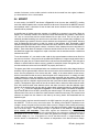
1
Laboratory Experiment 5
EE348L
Spring 2005
B. Madhavan
Spring 2005
B. Madhavan
Page 1 of 29
EE348L, Spring 2005
B. Madhavan
- 2 of 29-
EE348L, Spring 2005
Table of Contents
5
Experiment #5: MOSFETs ............................................................................5
5.1
Introduction ......................................................................................................................... 5
5.2
Theory................................................................................................................................. 5
5.2.1
MOSFET Basics ........................................................................................................ 5
5.3
MOS Capacitor ................................................................................................................... 6
5.4
MOSFET............................................................................................................................. 8
5.5
Biasing a MOSFET........................................................................................................... 10
5.6
A MOS current mirror ....................................................................................................... 11
5.7
MOSFET High-Frequency Model ..................................................................................... 12
5.8
Small Signal Canonic Cells of MOSFET Technology ...................................................... 16
5.8.1
Diode-connected MOSFET...................................................................................... 16
5.8.2
Common source amplifier canonic cell .................................................................... 17
5.8.3
Common drain amplifier canonic cell....................................................................... 18
5.8.4
Common gate amplifier canonic cell........................................................................ 19
5.9
MOSFET simulation in HSpice ......................................................................................... 20
5.10
Conclusion.................................................................................................................... 24
5.11
MOSFET Spice models................................................................................................ 24
5.12
Revision History ........................................................................................................... 24
5.13
References ................................................................................................................... 24
5.14
Pre-lab Exercises ......................................................................................................... 25
5.15
Lab Exercises............................................................................................................... 28
5.16
General Report Format Guidelines .............................................................................. 29
B. Madhavan
Page 3 of 29
EE348L, Spring 2005
Table of Figures
Figure 5-1: Schematic diagram of an NMOS and PMOS transistor. .............................................. 5
Figure 5-2: A cross-section of NMOS transistor in saturation......................................................... 6
Figure 5-3: A P-type MOS Capacitor. ............................................................................................. 7
Figure 5-4: Simulated iD-vDS characteristics of an n-channel MOSFET, 2N7000, for different gate
to source voltages. ................................................................................................ 10
Figure 5-5: Biasing a MOSFET. .................................................................................................... 11
Figure 5-6: MOS current mirror. .................................................................................................... 12
Figure 5-7: Large signal high frequency model of a MOSFET. .................................................... 13
Figure 5-8: Low frequency small signal MOSFET model. ............................................................ 14
Figure 5-9: A MOSFET connected as a diode. ............................................................................. 16
Figure 5-10: A Common-source amplifier. .................................................................................... 17
Figure 5-11: A small signal model of a common source amplifier. ............................................... 18
Figure 5-12: Common drain (or source-follower) canonic cell. ..................................................... 19
Figure 5-13: A common gate canonic cell..................................................................................... 20
Figure 5-14: HSpice netlist for obtaining I-V characteristic of an n-channel MOSFET, 2N7000. . 22
Figure 5-15: iD-vDS characteristics of MOSFET m1 in Figure 5-14 for gate to source voltages of 2,
3, and 4 volts. ........................................................................................................ 23
Figure 5-16: gm versus vDS characteristics of MOSFET m1 in Figure 5-14 for gate to source
voltages of 2, 3, and 4 volts. ................................................................................. 23
Figure 5-17: Pin diagram of the 2N7000 (Courtesy of Fairchild Semiconductor). ........................ 24
Figure 5-18: Circuit schematic for Laboratory experiment 5 pre-lab exercise 9 ........................... 26
Figure 5-19: A common source amplifier. ..................................................................................... 27
Figure 5-20: Circuit schematic for Laboratory experiment 5 exercise 1 ....................................... 28
B. Madhavan
- 4 of 29-
EE348L, Spring 2005
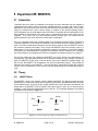
5 Experiment #5: MOSFETs
5.1 Introduction
Transistors are at the heart of integrated circuit design. As active elements, they are capable of
implementing gain stages, buffers, electrically operable switches, op-amps, and a host of other
applications. The word active refers to the fact that transistors require static power, from a power
supply for transistor bias current, and/or voltage, to operate in the desired operating region.
Circuit designers use the small-signal model of transistor for analysis that are appropriate for the
bias condition of that transistor. The static power is consumed so that the input signals may be
amplified. Thus, when one says that transistor-amplifier provides gain, one means that the
signals experience gain at the expense of static power consumption.
The most common commercial transistor today is the Metal-Oxide-Semiconductor Field-Effect
Transistor (MOSFET). Even though the MOSFET was conceived before the bipolar transistor, it
wasn’t until mature fabrications techniques and the digital revolution that the MOSFET became
the dominant transistor used today. Even though the MOSFET has been primarily used as a
digital device, it has made significant contributions to analog circuit design in recent times despite
its relatively poor transconductance compared to the Bipolar Junction Transistor (BJT), primarily
due to the needs for mixed signal circuit driven by integration of multiple functions on a single IC.
For the next couple labs, the operation of a MOSFET, as used in analog circuit applications, will
be presented. This experiment will deal with dc operation conditions, a.k.a. biasing, or quiescent
state, the MOSFET current mirror, and the canonic cells used in MOSFET amplifier design. As
will be seen, the MOSFET can be biased in one of three fundamental regions. This biasing will
determine the linearity of the MOSFET. The next laboratory experiment will deal with using the
canonic cells in combination to over come the intrinsic shortcomings of the stand-alone canonic
cells.
5.2 Theory
5.2.1
MOSFET Basics
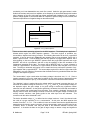
The MOSFET comes in two varieties, namely, NMOS and PMOS. This lab will primarily deal with
NMOS devices. It should be noted; that all equation presented for the NMOS transistor are valid
for the PMOS device, as long as all the voltage polarities and current directions are switched. As
stated above, the MOSFET must be biased in the proper regime in order for it to be used as an
amplifier, so this will be the fundamental focus of this lab. The schematic diagrams of an NMOS
and PMOS are presented in Figure 5-1.
Source
Drain
Gate
Gate
Bulk
Bulk
Drain
Source
PMOS
NMOS
Figure 5-1: Schematic diagram of an NMOS and PMOS transistor.
B. Madhavan
Page 5 of 29
EE348L, Spring 2005
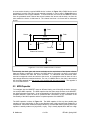
A cross-section showing a typical NMOS device is shown in Figure 5-2 (a PMOS device would
be identical, but with n-type and p-type materials reversed). It can be seen in Figure 5-2 that a
NMOS transistor has a P type substrate. To avoid confusion, the name for the MOSFET comes
from the generated carrier channel that occurs between the source and the drain, not from the
bulk material the device is fabricated in. The channel and how it is formed will be discussed
shortly.
Gate
Source
Drain
Metal
Gate oxide
N+
N+
Pinch-off
Channel of electrons
P substrate
Bulk
Figure 5-2: A cross-section of NMOS transistor in saturation.
Functionally, the drain, gate and source terminals are the equivalents of the bipolar collector,
base and emitter, respectively. However, the MOS device is symmetric, so there is no physical
difference between the drain and source terminals! To understand what determines which
terminal corresponds to drain and which to the source, an investigation must be done on how a
bias voltage affects the transistor behavior. For now, in a NMOS device, the drain is the terminal
will the higher potential and the source is the terminal with the lower potential. The opposite is
true for a PMOS device.
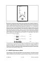
5.3 MOS Capacitor
To investigate how the MOSFET reacts to different biasing, we will simplify the device structure
into a simple MOS capacitor. The MOS capacitor has the exact same structure as the MOSFET,
but without the source and drain. As an understanding of this simplified model is developed, the
complete MOSFET model will then be presented with a discussion on the correlation of the
functionality of the MOS capacitor and the complete operation of the MOSFET.
The MOS capacitor is shown in Figure 5-3. The MOS capacitor is like any other parallel plate
capacitor you have seen before. It gets it name form the metal, oxide, semiconductor sandwich it is
comprised of. It should be noted that in today’s MOSFETs, the metal that makes up the top plate of the
capacitor is actually made out of poly-silicon, or poly. Poly is heavily doped silicon that has a high
B. Madhavan
- 6 of 29-
EE348L, Spring 2005
conductivity, so it has characteristics very much like a metal. Under the poly gate contact is oxide.
Oxide is an insulator, and just as in a capacitor, at low frequency no current flows through this insulator
(this is because of the very high band gap voltage associated with insulators). Like a capacitor, a
positive voltage applied to one terminal leads to a deposit of positive charge on that terminal, and
induces an equal amount of negative charge on the other terminal.
Gate
Oxide
Poly Silicon
P-type silicon
Bulk
Figure 5-3: A P-type MOS Capacitor.
There are three basic operating regimes for the MOS capacitor. The biasing that is applied to it
dictates which regime the MOS capacitor operates. The three regions of operation are:
accumulation, depletion and strong inversion. The following discussion will be for a p-type MOS
capacitor. It can be seen that in Figure 5-3 the capacitor has a p-type substrate, hence this is
where it gets its name. It will be shown later that the operation of p-type MOS capacitor has a
direct bearing on how an n-type MOSFET operates. Both the p-type MOS capacitor and n-type
MOSFET are built in a p-substrate, and this is why the operation of the first correlates to the
fundamental operation of the latter. The reason that a MOSFET built in a p-type substrate is
called an n-type MOSFET is because an n-type channel is formed under the gate, more on this
later. The thing to remember at this point is to be careful and not to confuse the operation of a ptype capacitor and a p-type MOSFET. The accumulation region will be the first region that will be
addressed in a p-type capacitor. We assume that the Bulk terminal is grounded and that the Gate
voltage is with respect to ground.
The “accumulation” region results when the biasing voltage is less than zero, VG < 0. Since a
negative potential is put on the metal gate just above the thin oxide, holes are attracted from the
bulk to the oxide and start to pile up, or “accumulate” a channel of holes at the oxide interface.
The “depletion” region is reached when the voltage applied to the gate is greater than zero, yet
less than the threshold voltage of the device, 0 < VG < Vth, where Vth is the threshold voltage. In
the depletion region, the gate voltage is not great enough to attract any significant number
electrons from the substrate. As the positive gate bias is increased, the holes that are located at
the oxide interface are pushed away from the oxide. Thus creating a “depleted” channel of the
majority carriers, holes, and creating a channel of fixed ions. As the gate voltage is increase, the
minority carriers, electrons, start getting pulled to the oxide layer form the substrate. This
continues until the device threshold is met.
The device threshold voltage, Vth, is defined as the voltage it takes to “invert” the channel under
the oxide of a p-type capacitor to an n+ concentration. At this point, the MOS capacitor has
reached “inversion”, VG > Vth. This condition is know as inversion because the applied bias has
attracted enough minority carriers, electrons, that the area directly under the oxide looks like an
n-material, thus it is inverted. One may ask, what is the difference between inversion and
depletion? In inversion the bias on the gate is large enough to attract a large and significant
B. Madhavan
Page 7 of 29
EE348L, Spring 2005
number of electrons, so the surface under the oxide is thus inverted from the original, unbiased,
p+ concentration to an n+ concentration.
5.4 MOSFET
A cross section of a MOSFET was shown in Figure 5-2. It can be seen that a MOSFET is nothing
more than a MOS capacitor with a source and drain at either end. Since half of the MOSFET structure
was explained earlier, a discussion of how the drain and source contribute to the functionality of the
transistor will be presented.
A simplified way of thinking about the operation of a NMOS is to compare it to a switch. When the
switch is “on” conduction needs to occur and thus current flows between two contacts. If the switch is
“off”, then no current flows and the switch behaves like an open circuit. Think of the gate as an
electrically activated switching lever and the source and drain as two contacts that just happen to be
heavily doped n-type material. Since the source and drain are comprised of n-type material, electrons
must be transported from source to drain for current to flow between them. Remember a MOS
capacitor with a gate bias that is equal or less than zero has a channel of holes at the oxide interface,
thus the same bias effectively places a barrier, a channel of holes, between the source and drain of a
NMOS. These holes block the transport of electrons and thus block the flow of current. Thus, when
the NMOS has a gate bias voltage that is equal or less than zero the transistor acts like a switch that
has been turned “off”.
To turn the transistor “on”, one needs to clear a path in the p-type substrate so electrons can flow from
the source to the drain. Going back to the operation MOS capacitor, if a large enough positive bias is
applied to the gate, then an inverted channel forms and becomes this desired path. Once the path is
created, an electric field from drain to source is needed to sweep the electron through the path. Thus,
two bias conditions must be met for the MOSFET to properly be turned “on”.
The picture gets a little more complicated when one considers the effect of the drain voltage. Ideally we
would like only the gate terminal to influence the current, thus the device would act like an ideal current
source from the perspective of the source and drain. Ideally, in the sense that this current source,
which is connected from drain to source, doesn’t depend on the voltage across it. In actuality, the drain
voltage impacts the current, but hopefully to a much lesser extent than the gate voltage. From earlier
discussions of diode, it should be clear that if the source sits at ground and the drain is at some positive
voltage, there will be a depletion region around the drain (note that the drain and substrate form a pn
junction). This depletion region wants to form all around the drain to where the drain meets the oxide;
since the inverted channel exists between source and drain, the result is that the depletion region
pinches off the channel right near the drain for gate-to-drain voltages less than the threshold voltage
(i.e., Vdg > -Vth). Pinch-off is highlighted in Figure 5-2. As the drain voltage is increased, the depletion
region extends farther from the drain, shortening the channel length. The obvious question is how do
electrons travel from source to drain if the channel doesn’t extend the entire way? The answer is that
electrons are swept from the channel to the drain by the strong electric field associated with the
depletion region.
Since the biasing regimes were discussed for the MOS capacitor, they will now be presented for
the MOSFET. To be sure, they are not the same. The biasing of the MOSFET depends on two
voltages, namely the gate-to-source and the drain-to-source voltages. When dealing with analog
circuits, one must ensure the biasing is correct for the desired operation, which more often than
not is the linear region. There are three region of operation for the MOSFET: cut-off, triode
(a.k.a. ohmic), and saturation. These three regions are determined by the two biasing
conditions stated above. Going back to the switch analogy, the gate-source voltage determines if
the device is “on” or “off”. Cut-off occurs when the gate-source voltage is less than the device
threshold voltage, Vgs < Vth. If the device is in cut-off, the drain current, Id, is approximately zero
and the device is considered off. This condition is independent of the drain-to-source voltage.
B. Madhavan
- 8 of 29-
EE348L, Spring 2005
Now the truth of the matter is the MOSFET doesn’t act like a perfect switch that turns off and on.
Current does flow in sub-threshold gate biasing, but for the purposes of this lab it will be assumed
the drain current is small and approximately zero when Vgs<0. The other two stages of operation
assume the gate-source biasing is above threshold (Vgs>0) and depend on the biasing of the
drain-source. The equations describing exactly how drain-source voltage influences channel
charge (and in turn the current) are incredibly complicated. However, simplified analysis shows
that the current depends roughly on the square of the gate voltage for Vds ≥ Vgs -Vt (saturation
region), and roughly linearly for Vds < Vgs -Vt (triode region). This assumes the devices are large
enough to avoid velocity saturation. Be careful not to confuse the linear current dependence of
the triode region with the linear operation of the device. When one talks about the linear
operation of the device, they are referring to the small-signal dynamic operation. This occurs
when the transistor is biased in the saturation region. Simulated iD versus vds curves for multiple
vgs voltages for a discrete n-channel MOSFET device, 2N7000, are shown in Figure 5-4. One
can see the two different operating conditions the MOSFET experiences as Vds is swept, namely
the triode and the saturation regions.
A summary of the three different operating regions and the associated drain current in each is
presented below for the NMOS. The equations below also hold for the PMOS transistor if the
polarity of all voltages is flipped. (Note: The threshold voltage, Vtp, for a PMOS is negative.)
NMOS:
I d ≈ 0,
Vgs < Vtn
(cut-off)
(5.1)
V
W
I d = K n Vds Vgs − Vtn − ds (1 + λnVds ),
2
L
K W
2
I d = n (Vgs − Vtn ) (1 + λnVds ),
2 L
Where
Vgs > Vtn ,
0 < Vds < Vgs − Vtn
Vgs > Vtn ,
(triode)
(saturation)
(5.2)
(5.3)
Vds > Vgs − Vtn
K n = µ n cox
cox =
ε ox
tox
(5.4)
(5.5)
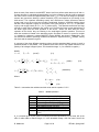
Table 5.1 summarizes the variables and their units used in equation 5.1-5.5.
Table 5-1
Vtn
W
L
λn
Kn=µncox
cox
tox
εox
MOSFET parameters
Threshold voltage for a NMOS [V]
Width of the transistor [µm]
Channel-length [µm]
Channel-length modulation [V-1]
Transconductance coefficient [A/V2]
Gate capacitance per unit area
Oxide thickness [µm]
Permittivity of the oxide (3.9)*8.85E-14
[F/cm]
Kn is a constant given by the product of mobility and oxide capacitance per unit area, W/L is the
ratio of oxide width to channel length, Vtn is the threshold voltage. One final note is that if the
B. Madhavan
Page 9 of 29
EE348L, Spring 2005
substrate is at a different voltage than the source, the threshold voltage varies due to the pn
junction between source and bulk. For this lab, the source and bulk will be tied together, so this
effect will be ignored.
To recap, for small-signal linear operation, one must ensure that the transistor is in the saturation
region. The goal and purpose of this lab is to bias the transistor in the linear region of operation,
so a small signal analysis may be preformed. Be careful not to confuse the nomenclature of the
operation of a MOSFET with the terminology used with bipolar transistor. For linear operation,
thus allowing the use of the small signal models, you want the MOSFET in the saturation region,
yet you will learn in future labs that you do not want a BJT in the saturation region. It is
unfortunate and sometimes confusing that both transistors use the same terminology for biasing
that yields in different small signal operation.
Figure 5-4: Simulated iD-vDS characteristics of an n-channel MOSFET, 2N7000, for different gate to source voltages.
Threshold shift
Many text books state equations that neglect the λn term in the equations above. They do this
because they have assumed that the bulk and the source are at the same potential. Since we
are using the 2N7000 for the purposes of this lab, these equations are perfectly reasonable. The
2N7000 is a three terminal device that has an internal connection between the source and drain,
so λn term may be neglected. However, for the sake of completeness, it should be noted that if
the drain and source aren’t at the same potential, then your circuit will experience a phenomena
that is known as the body effect. We won’t go into much detail of this second order effect in this
experiment, but it should be conveyed that this is an important issue when dealing with analog
integrated circuit design. A threshold voltage shift will result from a topology were the VSB is not
equal to zero.
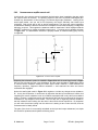
5.5 Biasing a MOSFET
This section will cover the biasing of an n-channel MOSFET amplifier shown in Figure 5-5. The
n-channel MOSFET is to be biased in the saturation region, at an operating point of desired drain
current, drain voltage, and gate voltage. The use of the quadratic relationship (equation 5.3)
requires knowledge of the mobility, oxide capacitance per unit area, the width and length of the
device, and the threshold voltage. For discrete components, these values vary too much for the
quadratic relationship to be a good predictor. One can measure these quantities in the laboratory,
but the idea here is to get a design that works without knowing all of the device parameters
B. Madhavan
- 10 of 29-
EE348L, Spring 2005
beforehand. For this example, let us assume that we looked up the data sheet of a discrete
MOSFET device that we are interested in, and determined that its threshold voltage, Vtn, is in the
range of 1V-to-3V. Remember that Vgs must exceed the threshold voltage, Vtn, for current to flow.
Say we desire a drain current of 1mA. We assume Vtn = 3.0V (worst case Vtn in range of 1V-3V).
We set Vgs = 3.25V so that we have Vgs- Vtn = 0.25V of worst-case gate-source overdrive voltage.
Next, a 3.75V gate voltage is arbitrarily chosen. Given that we want Vgs = Vg–Vs= 3.25V, this
dictates that Vs=0.5V. Using Ohm’s law, we get the source resistance, Rss = 0.5V/1mA = 500Ω.
Making sure the condition for saturation, Vds>= Vgs-Vtn, is satisfied, the drain voltage is chosen to
be 3.5V (Vds = 3.5V – 0.5V = 3.0V). With a supply voltage, Vdd=5V, and drain current of 1mA, this
requires a 1.5kΩ resistance (Rd) between the supply and the drain terminal. Next, in order to set
the gate voltage to at 3.75V, we use a voltage divider as shown in Figure 5-5 to derive Vg =
3.75V from the supply, Vdd=5V. The resistor ratio of Rb1: Rb2 needs to be 1:3. Therefore we set
Rb1=1kΩ and Rb2=3kΩ. Note that the bias network requires 1.25mA from the 5V supply!
For a MOSFET, the quadratic relationship dictates that the sensitivity of Id to Vgs is not as severe
as that of the I-V relationship of a diode, which is exponential. This means that Vgs has to vary a
great deal more than say, Vb, the applied voltage across a diode, for the same range of currents.
Sometimes, due to tolerances in fabrication, it can be tricky to achieve the exact biasing current.
However, a simple solution is to make one of the gate resistors, say Rb2, a potentiometer. This
allows one to tune and monitor the desired MOSFET performance.
Vdd
Rb1
Vdd
Rd
Rb2
Rss
Figure 5-5: Biasing a MOSFET.
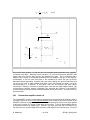
5.6 A MOS current mirror
The MOS current mirror discussed here is used to properly bias analog circuits. The strategy
invoked in a current mirror is to set a desired current, Iref, in one side and have that current
mirrored through another transistor. Current mirrors are used in circuit design so one can set a
specific current without disturbing the circuitry it that it is biasing. A current mirror is shown in
Figure 5-6. Notice that Iref is set in transistor M1, since transistor M1 and M2 have the exact same
Vgs, then the two transistors conduct the same amount of drain current. Hence Iref equals Iout.
This assumes the transistors are “matched”. When transistors are matched, then all their
parameters are equal (i.e. µn, cox, etc.). An analysis of a current mirror is left as a pre-lab
exercise.
B. Madhavan
Page 11 of 29
EE348L, Spring 2005
Vdd
R
Iref
M1
Iout
M2
Figure 5-6: MOS current mirror.
Note that M1 is a diode-connected transistor which guarantees that it operates in saturation, so
long as the gate voltage lies at least a threshold voltage above ground. The idea is that R is
chosen to establish the desired reference current in M1, and then M2 simply mirrors this current
exactly, as M1 and M2 have identical effective gate-source voltages (i.e., Vgs – Vt is identical for
both). In IC design, one has the additional benefit of being able to scale the reference current by
choosing M2 to have a larger gate aspects ratio (W/L) than the reference. In the lab we use
discrete components with fixed dimensions, so this seems like it would present some difficulty
when larger (W/L) ratios are desired. However, one may achieve a larger ratio by paralleling
devices. Some drawbacks to this approach include taking up a lot of space and being limited to
integer multiples of the reference current. The major problem with this current source (in the lab
and in IC design) lies in the dependence of the currents on Vds, which differs for each device.
Analysis of this current mirror leads to:
Vdd − I ref R = Vg1
(5.6)
K n1 W
(Vg1 − Vt )2 (1 + λ1Vg1 )
2 L
K n2 W
(Vg1 − Vt )2 (1 + λ2Vds 2 )
I out =
2 L
I ref
K 1 + λ1Vg1
= n1
I out K n 2 1 + λ2Vds 2
I ref =
(5.7)
(5.8)
(5.9)
Thus, the ratio is not 1:1 as is hoped. In IC design, the Kn factors will be very close, as matching
is a strong point of IC fabrication processes. However, in the lab and in IC design, regardless of
whether the lambda terms are equal, the drain-source voltages are necessarily different for
different drain resistances, making it impossible to match the currents over a wide range of loads.
In the lab, you will use a potentiometer for the load, and observe the variation in current as the
load, and hence the drain-source voltage, varies.
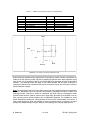
5.7 MOSFET High-Frequency Model
This experiment will build upon the concepts that were presented in the previous lab and
introduce dynamic circuits using MOSFETS. In the previous sections, we focused on properly
biasing the MOSFET and we learned that the purpose of biasing an analog circuit is so the active
B. Madhavan
- 12 of 29-
EE348L, Spring 2005
devices within the circuit operate in a desirable fashion (linear) on small signals that enter the
circuit. Once the MOSFET has been biased in the dynamic linear region, a.k.a. saturation, one
may use the large or small signal model developed to perform dynamic circuit analysis.
Signals are perturbations about the bias point (or quiescent point, a.k.a. Q-point) and carry all the
important information for your circuit to process. For instance, you might bias your input port at
2V, and then superimpose a 50 mV peak-to-peak sine wave to this bias voltage. Ideally, you
would like amplifiers to be perfect linear devices, meaning the output signal is some multiple of
the input signal, independent of the input amplitude. There are many ways that information is
modulated, but for the purposes of this experiment we will deal will strictly sinusoidal waves.
Transistors are normally non-linear devices (recall their I-V characteristics), so the device bias
point, and hence the gain, does depend upon the input amplitude. However, by suitably restricting
the amplitude of the input swing (using a “small signal”) and correctly biasing the circuit (Q point),
the resultant output will show very little distortion, meaning that the non-linear circuit acts
approximately linear for small-signal deviations about the bias point.
Drain
Dbd
rdd
Cgd
Gate
gmVgs
rbd
ro
gmbsVbs
Cbd
rbb
Bulk
Cbs
rbs
Cgs
Dbs
rss
Source
Figure 5-7: Large signal high frequency model of a n-channel MOSFET whose symbol is shown in Figure 5-1.
The MOSFET high frequency large-signal model is an empirical model and is shown in Figure
5-7. It is called a large-signal model because the values of model elements are dependent on the
dc bias voltage and current conditions of the device. In Table 5-2 you will find a list of what each
element represents in the MOSFET large signal model. As you can see all elements are
physical, unlike the BJT, which will be presented in future labs, where it is based off a Taylor
series expansion. The model in Figure 5-7 looks very complicated. This model can be simplified
for a first order analysis. If the signal of interest is a “small signal”, the frequency range of interest
is small enough and processing conditions are good, then many of the elements in Figure 5-7
maybe neglected for a simplified back of the envelope calculation. For many cases this first order
analysis is perfectly acceptable. If conditions arise where the model fails, then the insight learned
from it should be built upon and used to accurately account for any second order effects. A
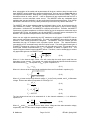
simplified NMOS low frequency small signal model is found in Figure 5-8.
B. Madhavan
Page 13 of 29
EE348L, Spring 2005
Table 5-2
MOSFET large-signal high-frequency model parameters
Element
Description
Element
Description
Cgs
Cgd
gm
gmbs
rdd
rss
ro
Gate Source Capacitance
Gate Drain Capacitance
Transconductance
Bulk-to-source transconductance
Drain resistance
Source resistance
Channel resistance
Dbd
Dbs
Cbs
Cbd
rbd
rbs
rbb
Bulk drain diode
Bulk Source diode
Bulk source capacitance
Bulk drain capacitance
Bulk drain resistance
Bulk source resistance
Distributed bulk resistance
Drain
Gate
gmVgs
λbgm Vbs
ro
+
Vgs
_
_
Vbs
Source
+
Bulk
Figure 5-8: Low frequency small signal MOSFET model.
Notice that all the capacitances are neglected in the low frequency model. Therefore, by definition, the
validity of the low frequency model is limited to operating frequencies where these capacitors act as
open circuits. For the purposes of this lab, the models and theory presented will focus on the NMOS
transistor. The following models also apply for the PMOS transistor with the slight modification of
reversing the direction of all controlled current sources and branch currents, and a reversal in polarity of
all port and branch voltages.
Note: The small signal model is just a tool that is used to help circuit designers analyze circuits utilizing
MOSFETs. Remember, this tool is only valid if the transistor is operating in the region of validity of its
small-signal model. Therefore it should be understood that when using the small-signal model,
significant effort has been made to ensure that the signal being processed in the amplifier is not too
large, ensuring that the dc-bias conditions are not significantly disturbed. This validates the “small
signal” assumptions, allowing the valid linearization of the non-linear characteristics of the device. A
large enough signal may cause the transistor to leave its linearized region of operation if its signal
change has a magnitude large enough to offset the set Q (biasing) point, causing signal distortion.
B. Madhavan
- 14 of 29-
EE348L, Spring 2005
Next, a description of the model and its parameters will be given, and then what is known as the
basic MOSFET canonic cells will be present and discussed. One can see from Figure 5-8 that at
low frequencies the MOSFET behaves like a voltage controlled current source (VCCS). This is a
little different than its cousin, the BJT. It will be presented in later experiments that the BJT is
treated like a current controlled current source. The MOSFET takes any modulated signal
applied to the gate and multiplies it by the small-signal forward transconductance. Even though
the MOSFET and the BJT are very closely related, they have some very distinct differences.
The MOSFET has an input resistance that is significantly higher. In fact, at low frequencies the
input resistance is infinite. The MOSFET has superior input signal to output current linearity
performance. Unlike the BJT, the MOSFET is a majority carrier device. Therefore, the MOSFET
experiences a negative temperature coefficient. Where any rise in temperature causes the output
current of a BJT to rise, the opposite is true for the MOSFET. In terms of power consumption, the
MOSFET also outperforms a bipolar device with lower power consumption.
About now one might be questioning why BJT transistors are still around if MOSFETS has so
many superior performance characteristics. The truth is the MOSFET does yield to the bipolar
devices in some analog performance categories. The MOSFET lacks the forward gain and
bandwidth that can be achieved with equivalent bipolar devices. The transconductance
generated by a BJT increased linearly with the Q-point current. The small signal forward gain of
a MOSFET increases at a factor of the square root of the Q-point current. This equation for the
small signal forward transconductance, gm, of a MOSFET is stated in equation 5.10. This
equation neglects channel length modulation effects. Therefore, it can be challenging to achieve
any appreciable gain out of a MOSFET circuit.
gm ≡
∂I D '
W
≈ 2Kn
∂Vgs Q − po int
L
I DQ
(5.10)
Where ID’ is the internal drain current. One will notice that the small signal model has two
dependent current sources. The second one models bulk effects and shows the bulk-to-source
transconductance, gmbs. The equation for gmbs is given in equation 5.11.
g mbs = λb g m
(5.11)
Where λb is known as the channel length modulation factor and it is defined in equation (6.3)
λb =
VΘ
2
2(VF − VT ) − VbsQ
(5.12)
Where Vθ is known as the body effective voltage, VF is the Fermi potential, and VT is Boltzmann
voltage. All three are defined in equations 5.13 through 5.15.
Vθ =
qN Aε s
2
Cox
(5.13)
N
VF = VT ln A
Ni
VT = 0.0259V
(5.14)
(5.15)
The last element that has to be accounted for is the channel resistance, ro. It is defined in
equation 5.16
'
1 ∂I D
≡
ro ∂Vds
=
Q − po int
I DQ
Vλ + VdsQ − VdssQ
(5.16)
Where VdsQ and VdssQ are defined as the drain source voltage and the drain saturation voltage,
respectively, and Vλ is the channel length modulation voltage.
B. Madhavan
Page 15 of 29
EE348L, Spring 2005
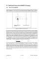
5.8 Small Signal Canonic Cells of MOSFET Technology
5.8.1
Diode-connected MOSFET
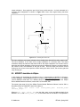
As stated in the previous lab, the MOSFET can be connected as a diode and this configuration is
shown in Figure 5-9. This circuit is very useful and common when biasing circuits. If you refer
back to section 5.6, one can see that every current mirror contains a diode-connected MOSFET.
+
+
Vds
rd
=>
_
Diode connected
MOSFET
Vds
_
Equivalent circuit
Figure 5-9: A MOSFET connected as a diode.
The diode-connected transistor is the simplest canonic cell for the MOSFET. The gate in Figure
5-9 is tied to the drain of the transistor, so it exhibits I-V behavior close to that of a conventional
PN junction diode. Tying the gate to the drain effectively makes the MOSFET a two-terminal
element. If one refers back to the cross sectional model of a MOSFET given in Figure 5-2, in
experiment 5, one can see that a p-n junction is formed between the substrate and the drain. The
affect of the n+ source is effectively nullified due to the source and bulk being tied to the same
potential. Notice when the MOSFET is connected in this configuration, it is guaranteed to be in its
saturation region. This two terminal device may be modeled as a two terminal resistor seen next
to it in Figure 5-9. Using the low-frequency small-signal model of MOSFET from Figure 5-8 and
neglecting channel resistance, the equivalent resistance of the diode-connected transistor can be
found to equal rd. The proof of equation 5.17 is left as a pre-lab exercise.
rd =
1
( λb + 1) g m
(5.17)
The next three canonic cells that will be presented are known as the common source, common
drain, and common gate. All three have applications in analog circuit design. They get their
respective names from the way they are connected. Ignoring the bulk terminal for a second, the
MOSFET effectively becomes a three terminal device. Each canonic cell will have a signal input
and signal output at one of the terminals. Since we are treating the MOSFET as a three terminal
device, one terminal is not used in part of the signal flow and thus is connected to ac ground.
This is where the canonic cells get their name. The terminal that is leftover is effectively the
common terminal.
B. Madhavan
- 16 of 29-
EE348L, Spring 2005
5.8.2
Common-source amplifier canonic cell
In this section, the common source is explored. Notice that the input is applied to the gate, while
the output is taken at the drain. The primary purpose of this cell is to provide small signal gain.
Another key characteristic of this topology is its inherent high output resistance. Looking at the
small signal model, one can see at low frequency the device effectively has infinite input
resistance. Both proofs will be left as pre-lab assignments. The input and output impedance
characteristics determine that the common source amplifier is best suited accepting a voltage and
delivering a current. This supports the statement made in experiment 5 which explained that the
MOSFET is effectively a voltage controlled current source. A common-source amplifier is shown
in Figure 5-10. It is assumed the transistor is properly biased, so external biasing (DC) circuitry
is neglected.
Vdd
Rl
Rin
Vo
Rout
Vs
Figure 5-10: A Common-source amplifier.
Replacing the schematic symbol of a NMOS in Figure 5-10 with the small signal model in Figure
5-8, one can calculate the gain, input impedance, and the output impedance. Figure 5-11 shows
a common-source amplifier utilizing the small signal model. However, it has assumed low
frequency operation, neglected channel resistance ro and assumed the drain and source
resistances are negligible.
Notice the small signal model in Figure 5-11 neglects to include any voltage source resistance,
Rs. At very low frequencies, it can be seen by inspection that the input resistance is infinite, thus
neglecting the source resistance is not an unrealistic assumption that is only valid in an academic
setting. However, at high frequencies, this assumption fails and one must account for the source
resistance for any analysis to be accurate. One can also see, if neglecting channel resistance,
that the resistance seen looking into the drain is also infinite at low frequencies. By inspection
you will notice that when looking into the drain one is staring at two current sources, thus the
resistance seen is ideally infinite.
The gain of the circuit is not as easily calculated as the input and output resistances, but simple
KVL and KCL equations should yield the following result.
B. Madhavan
Page 17 of 29
EE348L, Spring 2005
AV =
V0
= − g m Rl
Vs
(5.18)
Vdd
Rl
Vo
Rout
Rin
Vs
gmVgs
λbgmVbs
+
Vgs
_
Vbs
–
+
Figure 5-11: A small signal model of a common source amplifier.
One can see from equation 5.18 that the gain of this amplifier greatly depends on the resistance
connected to the drain. Referring back to equation 5.10, one can see that the MOSFET gate
aspect ratio (W/L) and the drain current, also determine the gain. This is comforting that a
designer has a variety of controllable parameters that can determine the gain of the topology.
Unfortunately, it can bee seen that some of the variables that control the gain are device
fabrication-process dependent. Problems may arise when dealing with process tolerances that
can be on the order of ±20%. Another draw back, which was pointed out earlier, is that the
transconductance of a MOSFET is well below what can be achieved with other device
technologies. Therefore, to achieve comparable gain, more than one stage maybe needed. The
common-source amplifier example presented here neglected the influence of the MOSFET
channel resistance and the external resistance between source and ground. This will be left as a
pre-lab exercise.
5.8.3
Common drain amplifier canonic cell
The next MOSFET canonic cell that will be presented will be the common drain amplifier, which is
commonly referred to as the source-follower amplifier as the voltage at the source terminal of the
MOSFET follows the voltage at the gate terminal. In this topology the input is once again applied
at the gate. However, the output is now taken at the source. It will be demonstrated that the
common drain acts like a voltage buffer. However, one major issue with this circuit arises from
the fact that it isn’t a great voltage buffer because it yields a gain that is less than unity. The proof
B. Madhavan
- 18 of 29-
EE348L, Spring 2005
of this is left as a pre-lab exercise. Even though the gain of this circuit is suspect, it can be shown
that like a voltage buffer the common drain topology has a large input impedance, and very small
output impedance. The common drain is shown in Figure 5-12. It is assumed that the transistor
is biased in the saturation region, so all biasing circuitry has been neglected.
Vdd
Rin
Vs
Rout
Vo
Rss
Figure 5-12: Common drain (or source-follower) canonic cell.
Replacing the MOSFET schematic symbol with its small signal model, neglecting ro, assuming
low frequency operation, the voltage gain, Av, input and output resistance are found to be:
V0
Rss g m
=
Vs 1 + Rss g m (1 + λb )
Rin = ∞
1
Rout =
g m (1 + λb )
AV =
(5.19)
(5.20)
(5.21)
Equations 5.19 through 5.21 show the common drain tries to emulate the characteristics of a
voltage buffer. However, it can be seen in equation 5.19, that the gain of this circuit can never be
unity. In fact, the solution for Av presented above was a first order calculation and thus neglected
higher order effects. Thus the gain predicted in equation 5.19 is a best case scenario and will
more than likely result in a gain that is larger than what you will physically measure in the lab.
From what you see in equation 5.19 it will be your job in the pre-lab to speculate where the
potential pitfalls may lie in its derivation.
5.8.4
Common gate amplifier canonic cell
The last canonic cell presented in the common gate. Notice in this configuration that the input is
connected at the source, while the output is taken at the drain. The common gate finds utility as
a current buffer. One will discover that it has unity current gain, low input resistance, and high
B. Madhavan
Page 19 of 29
EE348L, Spring 2005
output resistance. Once again the proof is left as a pre-lab exercise. A circuit schematic of a
common gate configuration is shown in Figure 5-13. Note: Once again biasing has been
neglected.
Vdd
Rl
Io
Vo
Rout
Rin
Rs
Is
Figure 5-13: A common gate canonic cell.
The input resistance and output resistance have already been derived from other canonic cells.
The input resistance is the same as the output resistance of a common drain. The output
resistance exactly the same as what was found for the output resistance of a common source.
Assuming the internal resistance of the current source is ideal and if there are no other paths for
the current to flow, the calculation of the gain is trivial. One can simply see that the current
flowing into the source must equal the current leaving the drain. Hence, the common gate has
unity current gain.
5.9 MOSFET simulation in HSpice
In this section, we investigate the simulation of the I-V characteristics of 2N7000, a discrete nchannel MOSFET, whose datasheet may be found at (http://www.supertex.com ). An HSpice
Level-3 MOSFET model deck for a different device is available on page 8-93 of the HSpice
Device Models Reference Manual, version 2001.4, December 2001.
The syntax (see page 8-14 of the HSpice Device Models Reference Manual, version 2001.4,
December 2001) for a MOSFET element in HSpice is:
mxxx
drain gate source bulk mosfet_model_name. W=mosfet_width
L=mosfet_length
Where drain, gate, source, bulk are the drain, gate, source and bulk terminals of the
MOSFET mxxx, and mosfet_model_name is the model name of the MOSFET as specified in
B. Madhavan
- 20 of 29-
EE348L, Spring 2005
the HSpice MOSFET model deck. W and L are the width and length of the MOSFET respectively,
specified in units of meters.
$
Very Important Point:
See pages 4-18 to 4-20 of the HSpice user manual, version 2001.4, December 2001;page 8-14
for the general MOSFET model statement, pages 8-21 to 8-26 for the MOSFET equivalent
circuits, 8-59 to 8-101 for MOSFET capacitance models, and pages 9-20 to 9-33 for the Level 3
MOSFET model deck, in the HSpice Device Models Reference Manual, version 2001.4,
December 2001
The simulation of semiconductor devices requires the specification of an appropriate device
model deck in HSpice. The model deck specifies a particular mathematical model of the device
being simulated and the values of the parameters associated with the model. Model parameter
values that are not specified default to the default values specified in HSpice. The interested
reader can determine the default values associated with a particular model by searching the
HSpice Device Models Reference Manual, version 2001.4, December 2001.
An example of an HSpice model deck specification for 2N7000, the discrete n-channel MOSFET
used in this laboratory assignment, is shown below. The model deck is obtained from
www.supertex.com. Note that the model deck starts with the keyword .MODEL, followed by the
particular n-channel MOSFET model name, nmos_2N7000, followed by the keyword NMOS. The
“+” character is a continuation character that indicates that the model deck specification continues
on that line.
.MODEL nmos_2N7000
NMOS
+LEVEL=3
RS=0.205
+DELTA=0.1
KAPPA=0.0506
+RD=0.239
VTO=1.000
+NFS=6.6E10
TOX=1.0E-7
+XJ=6.4666E-7
THETA=1.0E-5
$
NSUB=1.0E15
TPG=1
VMAX=1.0E7
LD=1.698E-9
CGSO=9.09E-9
CGDO=3.1716E-9
ETA=0.0223089
UO=862.425
Very Important Point:
It is very important to start the model deck with the .MODEL keyword, followed by the mosfet
model name and then the keyword NMOS for an n-channel MOSFET. It is good practice to put
the device models at the end of the netlist before the final .END statement.
The internal model variables of the MOSFET model may be plotted or used in expressions. The
internal model variables that are accessible to the user are detailed on pages 8-63 to 8-65 of the
HSpice user manual, version 2001.4, December 2001.
Figure 5-14 is an example of a netlist that can be used to plot the iD-vDS characteristics of the
MOSFET 2N7000, specified by the model deck named nmos_2N7000 in Figure 5-14. The drain
to source voltage, vDS, is swept from 0V through 5V in steps of 0.01V at gate to source voltages,
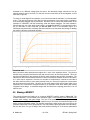
vGS of 2V, 3V, and 4V. The HSpice simulation results are shown in Figure 5-15. Refer to
Laboratory assignment 3 or the HSpice user manual, version 2001.4, December 2001 for help on
plotting using mwaves/awaves.
MOSFET I-V characteristic
*Written Feb 24, 2005 for EE348L by Bindu Madhavan.
******************************************************
**** options section
******************************************************
.options post=1 brief nomod alt999 accurate acct=1 opts dccap=1
B. Madhavan
Page 21 of 29
EE348L, Spring 2005
******************************************************
**** circuit description
******************************************************
m1 drain gate source bulk nmos_2N7000 W=0.8E-2 L=2.5E-6
******************************************************
**** sources section
******************************************************
vdrain drain vss 5V
vsource source vss 0V
vbulk
bulk
vss 0V
vgate
gate
vss 1V
v2
vss
0
0V
******************************************************
**** specify nominal temperature of circuit in degrees C
******************************************************
.TEMP=27
******************************************************
**** analysis section
******************************************************
.dc vdrain 0 5.0 0.01 sweep vgate poi 3 2.0 3.0 4.0
******************************************************
**** probe statement section
******************************************************
*see pages 8-63 to 8-66 of HSpice user manual, Version 2001.4
.probe dc idrain
= par('id(m1)')
.probe dc cgd
= par('-lx19(m1)')
.probe dc cgs
= par('-lx20(m1)')
.probe dc cgtotal
= par('lx18(m1)')
.probe dc vthreshold = par('lv9(m1)')
.probe dc vdsat
= par('lv10(m1)')
.probe dc gm
= par('lx7(m1)')
.probe dc gmbs
= par('lx9(m1)')
.probe dc gds
= par('lx8(m1)')
.probe dc rds
= par('1/lx8(m1)')
******************************************************
**** models section
******************************************************
*(this Model is from supertex.com)
.MODEL nmos_2N7000
NMOS
+LEVEL=3
RS=0.205
NSUB=1.0E15
+DELTA=0.1
KAPPA=0.0506
TPG=1
CGDO=3.1716E-9
+RD=0.239
VTO=1.000
VMAX=1.0E7
ETA=0.0223089
+NFS=6.6E10
TOX=1.0E-7
LD=1.698E-9
UO=862.425
+XJ=6.4666E-7
THETA=1.0E-5
CGSO=9.09E-9
.END
Figure 5-14: HSpice netlist for obtaining I-V characteristic of an n-channel MOSFET, 2N7000.
B. Madhavan
- 22 of 29-
EE348L, Spring 2005
vGS=4V
vGS=3V
vGS=2V
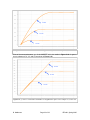
Figure 5-15: iD-vDS characteristics of MOSFET m1 in Figure 5-14 for gate to source voltages of 2, 3, and 4 volts.
Plots of the transconductance, gm, of the MOSFET m1 in the netlist in Figure 5-14 for gate to
source voltages of 2V, 3V, and 4V are shown in Figure 5-16.
vGS=4V
vGS=3V
vGS=2V
Figure 5-16: gm versus vDS characteristics of MOSFET m1 in Figure 5-14 for gate to source voltages of 2, 3, and 4 volts.
B. Madhavan
Page 23 of 29
EE348L, Spring 2005
5.10 Conclusion
MOSFETs are the most commonly used semiconductor today in integrated circuit design. A
circuit designer must bias the MOSFET correctly to ensure small-signal linear operation. If not
biased properly, distortion will hinder the design. The next lab will assume that the MOSFET is
biased in the saturation region and deal primarily with dynamic operation and the small-signal
model.
The MOSFET canonic cells behave very analogous to the BJT canonic cells. The absolute
values and expressions found for the gain, input resistance, and output resistance may differ, but
the point is the canonic cells of both technologies have remarkably close behavior. However,
don’t fall in the trap of just replacing MOSFET with BJT, or vice versa, in known topologies and
expect the circuit to behave the same way. As one matures in circuit design, you will see that
many factors result in topologies that produce the same result are structurally very different for
MOSFET and BJT implementation. For example, biasing is dealt with very differently for these
two topologies.
5.11 MOSFET Spice models
*(this Model is from supertex.com)
.MODEL NMOS_2N7000
NMOS (LEVEL=3
RS=0.205
+DELTA=0.1
KAPPA=0.0506
TPG=1
+RD=0.239
VTO=1.000
VMAX=1.0E7
+NFS=6.6E10
TOX=1.0E-7
LD=1.698E-9
+XJ=6.4666E-7
THETA=1.0E-5
CGSO=9.09E-9
+W=0.8E-2)
NSUB=1.0E15
CGDO=3.1716E-9
ETA=0.0223089
UO=862.425
L=2.5E-6
Figure 5-17: Pin diagram of the 2N7000 (Courtesy of Fairchild Semiconductor).
5.12 Revision History
This laboratory experiment is a modified version of the laboratory assignment 5 (MOSFET Static
Operation) and laboratory assignment 6 (MOSFET Dynamic circuits) created by Jonathan
Roderick.
5.13 References
[1]
Avant! HSpice User Manual, Version 2001.4, December 2001, posted on EE348L class web
site.
B. Madhavan
- 24 of 29-
EE348L, Spring 2005
[2]
Avant! HSpice Device Models Reference Manual, Version 2001.4, December 2001, posted on
EE348L class web site.
[3]
Bindu Madhavan, EE348L Laboratory Experiment 3, Spring 2005.
[4]
Gerald W. Neudeck. Volume II The PN Junction, Addison-Wesley Publishing Company,
Reading, Massachusetts, 1989.
[5]
Ben G. Streetman. Solid State Electronic Devices. Prentice-Hall Inc., Englewood Cliffs, New
Jersey, 1990.
[6]
Richard C. Jaeger. Introduction to Microelectronic Fabrication. Addison-Wesley Publishing
Company, Reading, Massachusetts, 1993.
[7]
S. M. Sze. Physics of Semiconductor Devices. John Wiley & Sons, Inc., New York, 1981.
[8]
Paul R. Gray & Robert G. Meyer. Analysis and Design of Analog Integrated Circuits. John
Wiley & Sons, Inc., New York, 1993.
5.14 Pre-lab Exercises
Note:
•
•
•
•
For HSpice simulations, use the model deck for 2N7000 in Figure 5-14
See HSpice guidelines in Laboratory Experiment 3.
Submit plots relevant to each question in your lab report.
Pre-lab questions 6, 7, 8, 9, and 10 are to be turned in as homework assignment.
1)
Plot the parameters rds, vthreshold, and cgtotal in the netlist in Figure 5-14. In
your plots, specify the range of values of vDS in which rds correspond to a linear resistor
for different values of vGS?
2)
If given a plot of √ids versus vGS for a NMOS transistor biased in the saturation region,
Cox, and W/L, derive an expression to calculate the mobility of electrons [cm2/Vs], µn.
Could you also determine the threshold voltage [V], Vtn, from this data? If so, how? For
both calculations assume that the channel length modulation is negligible, i.e., λn=0 in
equation 5.2 and equation 5.3.
3)
Given Kn(W/L)=5E10-3 A/V2, Vtn=1.2V, and λn=0.002V-1 use Excel, or an equivalent, to
plot iD versus vGS for a given vDS that assures the transistor stays in the saturated region.
Make sure data points are calculated for vGS from 0V to 5V in steps of 0.5V. Using the
plot so obtained, determine the transconductance, gm [mS], for each ∆vGS region of 0.5V
from 0V to 5V, using the equation below. Plot gm versus the gate-source voltage vGS.
gm =
4)
Vds = cons tan t
I − I d1
= d 2
V −V
gs1
gs 2
Vds = cons tan t
Given Kn(W/L)=5E10-3 A/V2, Vtn=1.2V, and λn=0.002V-1 use Excel, or an equivalent, to
calculate and plot iD versus vDS for various gate-source voltages, varying vGS from 0.5V to
5.0V in steps of 0.5V (10 vGS data points). Use vDS1=6.5V and vDS2=9.0V and calculate
the corresponding drain currents. Use these data points to calculate the drain-to-source
conductance, gds [mS], using the equation below. Plot the ten data points of gds so
obtained against the gate-source voltage, vGS.
g ds =
5)
∂I ds
∂Vgs
∂I ds
∂Vds
Vgs = cons tan t
I − I d1
= d 2
Vds 2 − Vds1 Vgs =cons tan t
As a circuit designer, it is sometimes advantageous to find the optimum biasing condition
for a MOSFET. The optimum biasing condition occurs when gm is maximized and gds is
B. Madhavan
Page 25 of 29
EE348L, Spring 2005
minimized simultaneously. Used the data you calculated to plot the ratio gm/gds versus
vGS. What is the optimal biasing voltage range for the transistor?
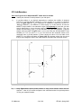
Vdd
Rl
Vo
Rout
Rin
Vs
Rss
Figure 5-18: Circuit schematic for Laboratory experiment 5 pre-lab exercise 9
6)
The example of the common-source amplifier in Figure 5-10 neglected the drain-tosource resistance, ro (= 1/gds), and any external resistance connected between the source
terminal and circuit ground. Figure 5-18 features a common-source amplifier with an
external source resistance, Rss. Re-derive the gain of the common-source amplifier,
taking into account the drain-to-source resistance, ro (= 1/gds), and the external resistance
Rss. Notice that the bulk and the source terminals are not at the same potential. The bulkto-source transconductance, gmbs, must be taken into consideration during the smallsignal analysis. How did the external source resistance affect the gain of the commonsource amplifier?
7)
It was stated that the common-drain amplifier in Figure 5-12 has less than unity gain.
From what you see in equations 5.19 through 5.21, can you speculate why? Derive the
gain, and output resistance of a common-drain amplifier without neglecting the drain-tosource resistance, ro. Did including the drain-to-source resistance ro, make this canonic
cell perform better or worse as a voltage buffer (compared to what was derived in
equations 5.19 through 5.21 when channel resistance, ro, was neglected)?
B. Madhavan
- 26 of 29-
EE348L, Spring 2005
Vdd
Rb1
Vdd
Rd
Rout
Cc
Vout
Rin
Cc
Vs
Rb2
Rss
Figure 5-19: A common source amplifier.
8)
Using what you have learned, calculate the transconductance (gm) of the transistor and
the voltage gain (AV) of the common-source amplifier whose schematic is shown in
Figure 5-19, which is based on the biasing example in Figure 5-5. Hence you will
measure the output at the drain and input your signal at the gate. Be sure to use
coupling capacitors, Cc, so that the biasing of the circuit is not disturbed. Assume that the
coupling capacitors, Cc, act as short circuits at the frequency of the input signal. Verify
your results in HSpice.
9)
It was discussed earlier that the input resistance and output impedances of a common
source amplifier are ideally infinite. Assuming the coupling capacitors, Cc, act like a short
circuit at the frequency of the input signal, is this still the case once the biasing resistors
are taken into consideration? Calculate the input and output impedances of the commonsource amplifier topology seen in Figure 5-19. Do your calculations agree with what was
stated earlier in this experiment? Why or why not?
10)
Move the output from the drain to the source of the MOSFET in Figure 5-19. Calculate
the voltage gain of the circuit. Verify your results in HSpice. What canonic cell is this
topology?
B. Madhavan
Page 27 of 29
EE348L, Spring 2005
5.15 Lab Exercises
Note: See Figure 5-14 for HSpice MOSFET model deck for 2N7000.
• Submit plots relevant to reach question in your lab report.
1)
In pre-lab problem 2, you derived expressions to calculate the mobility of electrons
[cm2/Vs], µn, and the threshold voltage [V], Vtn from a graph of √ids versus vGS. Build the
circuit in Figure 5-20 with Vdd=5V, determine all resistances needed (see section 5.5,
“Biasing a MOSFET”), and measure iDS while varying vGS. In this exercise, be sure the
MOSFET stays biased in the saturation region (by adjusting V1) and that you take
enough data points to get an accurate model of the iDS versus vGS behavior. Plot your
results, and calculate µn and Vtn for this transistor using the data collected. From the
HSpice netlist provided in Figure 5-14, it can be seen that the 2N7000 MOSFET has
W=8000 µm, L=2.5 µm, and Tox= 0.1 µm. How close are the measured values to the
calculated ones in pre-lab problem 2? Does varying the value of W, the width of the
MOSFET, in an HSpice simulation of Figure 5-20, with element values from the circuit
that you have designed, improve the match between simulated and measured results?
Vdd
Rb1
Rl
V1
+
+
Vds
Vgs
_
_
Rb2
Figure 5-20: Circuit schematic for Laboratory experiment 5 exercise 1
2)
Using Figure 5-20, repeat pre-lab problem 3, using circuit element values from lab
exercise 1. How do your results compare to the calculated results from pre-lab problem
3? Plot your measured results.
B. Madhavan
- 28 of 29-
EE348L, Spring 2005
3)
Using Figure 5-20, repeat pre-lab problem 4, using circuit element values from lab
exercise 1 above. How do your results compare to the calculated ones from pre-lab
problem 4? Plot your measured results.
4)
Using the results from lab exercises 2 and 3 above, use the procedure in pre-lab problem
5 to determine the optimal biasing voltage range from measured data. Plot your results.
5)
Build and verify the biasing example that was presented for a MOSFET in Figure 5-5.
Take care that you look up the manufacturer’s datasheet to determine the
threshold voltage range (minimum, typical, and maximum values) of the particular
discrete MOSFET device that you are using. Are your measured results with in ±2% of
the specifications the circuit was designed for? If not, adjust resistor values until they do.
Record any changes that you made. From what you have learned, can you speculate
why there were discrepancies between theory and measured data?
6)
Build the circuit in Figure 5-19. Apply a 50mV peak-to-peak 4kHz sinusoidal signal at the
input. Measure the output signal at the drain of the MOSFET. Do your results agree with
your calculations and HSpice results from pre-lab question 8? Why or why not?
7)
Using the same circuit, connect a load of 1Meg Ohm at Vout. Measure the output signal at
the drain of the MOSFET, and calculate the gain. Did your results change from what you
observed in the previous exercise? If so, why? Repeat this procedure for load values of
50k, 5k, 1k, 500, and 50 ohms. Did your results change for any of these values? If so,
why? Does this confirm your answer to pre-lab problem 5?
8)
Design a common source amplifier that has 1mA of drain current, but double the gain as
the circuit from lab exercise 6. Propose three different solutions for achieving this goal.
What parameters and/or circuit elements can you use to accomplish this? Do any of the
three solutions violate limitations of the device (i.e. current limitations which is 200mA,
power limitations which is 200mW for a 2N7000)? If they are physically possible, verify
the operation of your purposed solutions.
5.16 General Report Format Guidelines
1. Data
Present all data taken during the lab. It should be organized and easy to read.
2. Discussion
Answer all the questions in the lab. For each laboratory exercise, make sure that
you discuss the significance of the results you obtained. How do they help your
investigation? Explain the meaning, the numbers alone aren’t good enough.
3. Conclusion
Wrap up the report by giving some comments on the lab. Do the results clearly
agree with what the lab was trying to teach? Did you have any problems?
Suggestions?
B. Madhavan
Page 29 of 29
EE348L, Spring 2005