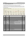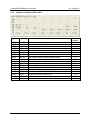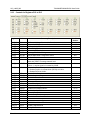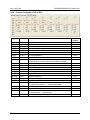
1
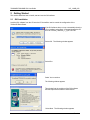
73M1866B/73M1966B GUI User Guide March 23, 2009 Rev. 1.1 UG_1x66B_002 73M1866B/73M1966B GUI User Guide UG_1x66B_002 © 2009 Teridian Semiconductor Corporation. All rights reserved. Teridian Semiconductor Corporation is a registered trademark of Teridian Semiconductor Corporation. Windows is a registered trademark of Microsoft Corporation. All other trademarks are the property of their respective owners. Teridian Semiconductor Corporation makes no warranty for the use of its products, other than expressly contained in the Company’s warranty detailed in the Teridian Semiconductor Corporation standard Terms and Conditions. The company assumes no responsibility for any errors which may appear in this document, reserves the right to change devices or specifications detailed herein at any time without notice and does not make any commitment to update the information contained herein. Accordingly, the reader is cautioned to verify that this document is current by comparing it to the latest version on http://www.teridian.com or by checking with your sales representative. 2 Rev. 1.1 UG_1x66B_002 73M1866B/73M1966B GUI User Guide Table of Contents 1 Introduction ................................................................................................................................... 5 2 Getting Started............................................................................................................................... 6 2.1 GUI Installation ........................................................................................................................ 6 2.2 Using the GUI .......................................................................................................................... 8 2.2.1 Controls for Registers R00 to R09 ............................................................................... 11 2.2.2 Controls for Registers R0A to R12 .............................................................................. 12 2.2.3 Controls for Registers R13 to R1C .............................................................................. 13 2.2.4 Controls for Registers R1D to R23 .............................................................................. 15 3 Scripts .......................................................................................................................................... 16 4 Related Documentation ............................................................................................................... 18 5 Contact Information..................................................................................................................... 18 Revision History .................................................................................................................................. 18 Rev. 1.1 3 73M1866B/73M1966B GUI User Guide UG_1x66B_002 Figure Figure 1: Register Access Screen – R00-R09 Tab ................................................................................... 8 Table Table 1: GUI Controls .............................................................................................................................. 9 4 Rev. 1.1 UG_1x66B_002 73M1866B/73M1966B GUI User Guide 1 Introduction The 73M1866B/73M1966B Graphical User Interface (GUI) provides control of the 73M1866B and 73M1966B registers. The GUI is used to configure the 73M1866B and 73M1966B demo boards and to read the status conditions of these boards. This document applies to GUI software version 1.3. The GUI can be use with either the Demo Board or the Keychain Board. The GUI cannot be used if the SPI is connected to a host device. For example, if a Keychain Board is embedded in an application, use the appropriate driver (MIPS, ARM, etc.) to configure the Keychain Board. ® Install the GUI on a PC running Microsoft Windows versions XP, Me or 2000. The installation requires one megabyte of disk storage. In this user guide, the 73M1866B and 73M1966B will be collectively referred to as the 73M1x66B. The FPGA controls are not for customer use. Do not change the parameters on the FPGA tab. Similarly, do not select FPGA Functions from the Controls menu or use the functions on the FPGA Memory Functions screen. Rev. 1.1 5 73M1866B/73M1966B GUI User Guide UG_1x66B_002 2 Getting Started This section describes how to install, start and use the GUI software. 2.1 GUI Installation Load the GUI software from the CD onto the PC that will be used to control the configuration of the 73M1x66B Demo Board. If the GUI software does not run automatically when the CD is installed, select Start Run and browse the CD drive for Teridian_73M1966_1_3_SETUP.EXE. Select OK. The following window appears. Select Run. Select Yes to continue. The following window appears. This window lists the revisions of the GUI software and the improvements made in each revision. Select Next. The following window appears. 6 Rev. 1.1 UG_1x66B_002 73M1866B/73M1966B GUI User Guide This window shows the default destination for the GUI software Select Next. The following window appears. The user can change the destination folder from the default. Change the destination folder or select Next to accept the default folder. The GUI software loads into the specified folder and the following window appears. The setup is complete. Click Finish. The software is ready for use. Rev. 1.1 7 73M1866B/73M1966B GUI User Guide 2.2 UG_1x66B_002 Using the GUI The 73M1866B or 73M1966B Demo Board must be set up before using the GUI. See the 73M1866B/73M1966B Demo Board User Manual for setup procedures. To start the GUI using Windows XP, select Start All Programs Teridian Teridian 73M1966B. The Register Access screen appears (see Figure 1). The screen is divided into a top half and a bottom half. The first row of the top half consists of five tabs: R00-R09, R0A-R12, R13-R1B, R1C-R25 and FPGA. The R00-R09 tab displays the register map for the first ten 73M1966B registers. The contents of each named bit can be changed by checking or un-checking the box next to it. A checked box means that the bit is set to 1 and an un-checked box means that the bit is set to 0. As boxes are checked and unchecked, the values in the bottom half reflect the changes and turn red. Select new values by checking and un-checking register bits. Click the Write Red button to set the values. Notice that after writing the values, all previously red values turn black. Polling can be done by double clicking on the lower register map for the register you are interested in or using the “Read All” radio button. Figure 1: Register Access Screen – R00-R09 Tab 8 Rev. 1.1 UG_1x66B_002 73M1866B/73M1966B GUI User Guide The bottom half of the Register Access screen shows the status of the entire 73M1x66B register set (in hex) and provides information and parameter controls. Table 1 describes these controls. Table 1: GUI Controls Click Write Red to write all red values in the bottom half of the screen. Values become red when changed by checking or un-checking boxes in the top half of the screen. Click Write all to write all values (both read and black). After writing values, all values become black and remain black until another box is checked. Click to read all current values from the board. Select BRCT (BroadCasT) to send the same control data to all the 73M1966Bs in a daisy chain, ignoring their individual addresses. When using the 73M1966B in daisy chain mode, it is necessary to set the address of the 73M1966B that is being accessed. Each board has a 73M1906B and FPGA address. For example, the next downstream daisy chained 73M1966B board will have an address for its 73M1906B of 03h and its FPGA address will be 04h, and so on. See Section 5 of the 73M1866/73M1966 Data Sheet for a description of the control byte and the BRCT bit. The radio buttons allow the selection of 8-bit or 16-bit SPI operations. Implements the POLL function as described in Section 6.1 of the 73M1866B/73M1966B Data Sheet. The Index field corresponds to the INDX field (Register 0x19[3:0]). The Value field corresponds to the POLVAL field (Register 0x1F[7:0]). Index is the offset address of the register to be manually polled with the results placed in POLVAL. The Index value ranges from 0 to 6 only. Index 0 refers to Register 0x12, Index 1 to Register 0x13, etc. The Value field returns the content of the register corresponding to the specified Index. Enter the index in the Index box. Select Poll. When this register is polled, the value is read back in the Value box. After selecting Poll, a red dot next to Match means that the register was not properly written. A green dot proves that the register was properly written. Sets the registers to a default operating configuration. This is not the same as the default register settings after the 73M1x66 goes through a device reset. The default register settings may not be appropriate for all PCM test sets, so you may define your own default operating conditions. Rev. 1.1 9 73M1866B/73M1966B GUI User Guide UG_1x66B_002 Sets the registers to a user-defined configuration contained in a specified script file. This is used to quickly put the registers into a configuration and the 73M1x66 into operational mode without having to individually set the register bits. If you have a configuration that you will use again later, the configuration can be saved as a script. See Log All Register Accesses to File. Used to keep a record of all register accesses performed by the user. Once turned on, user transactions are recorded in the file specified in the window. This is used to record a sequence of operations that can be edited and saved as a script. To use the recorded configuration, see Reset to Script File. If Log Status is checked, all SPI transactions are recorded in the specified file, including those generated by the background line condition monitoring routine (line voltage, current, etc.). If Log Status is checked and line condition monitoring is activated, be aware that the log file is continuously increasing in size. The settings for the three most common termination impedances. These are U.S. (600 Ω), CTR-21 (complex) and Australian (Australian complex). Select one to set the termination impedance. After activating the Read All radio button, the currently valid impedance is indicated only if it is one of the three choices. If the currently valid impedance is not one of the three choices, none of the options will be shown as active. Goes Off-Hook. Goes On-Hook. Calibrates the receive channel of the chipset. If the SPI transactions are corrupted for some reason, pressing this button resets the 73M1966B SPI state machine and restores proper communication between the 73M1966B and the GUI. Updated with the most recent ring signal voltage as measured in R1A. This measurement is only valid during the on-hook state. Displays the DC voltage and DC current from the CO or line emulator. The current reading is valid in off-hook mode only. Stops the continuous line condition monitoring routine. Line voltage, current, etc. will not be written to the log file. Starts the continuous line condition monitoring routine. Line voltage, current, etc. will be written to the log file. 10 Rev. 1.1 UG_1x66B_002 73M1866B/73M1966B GUI User Guide 2.2.1 Controls for Registers R00 to R09 The GUI represents 73M1x66B registers in the form Rhh, where hh is the hexadecimal address. The 73M1866B/73M1966B Data Sheet represents these same registers in the form 0xhh. For detailed descriptions of 73M1x66B registers, see the 73M1866B/73M1966B Data Sheet. The tables below list the section numbers in the 73M1866B/73M1966B Data Sheet where additional information can be found about each bit. Register Bit Name R02[7] R02[2] R03[7:5] R03[4] R03[3] R03[2] R03[1] R03[0] TMEN ENLPW GPIOn PCLKDT RGMON DET SYNL RGDT R04[7:5] DIRn R04[3:0] R05[7:5] R05[4] R05[3] R05[2] R05[1] R05[0] R06[7:5] R07[1:0] R08 R09 REVHSDn ENGPIOn ENPCLKDT ENAPOL ENDET ENSYNL ENRGDT POLn DTSTn TXDGn RXDGn Rev. 1.1 Summary Description Test Mode Enable Enable Line Power GPIO Pin Enable PCLK Error Detected Ringing Monitor – 0 = silent, 1 = ringing Voltage Detection – 1 = detection of one of three conditions Barrier Synchronization Loss has occurred Ring or Line Reversal Detection – 1 = a Latched Ring or Line Reversal Detection event GPIO Input/Output Select – 0 = GPIO pin is an output, 1 = GPIO pin an input Host-Side Device Revision GPIO Enable Enable PCLK Detection Enable Automatic Polling Enable Voltage Detection Enable Synch Loss Detection Enable Ring Detection Interrupt GPIO Interrupt Edge Selection Digital Test Mode Select Transmitter Digital Receiver Digital Gain Data Sheet Section 12.7 9.5 7.5 8.8 11.12 11.12 9.5 11.12 7.5 7.1 7.5 8.8 9.5 11.12 9.5 11.12 7.5 12.7 8.8 8.8 11 73M1866B/73M1966B GUI User Guide UG_1x66B_002 2.2.2 Controls for Registers R0A to R12 Register R0D[7] R0D[6] R0E[7] R0E[1:0] R0F[7] R0F[6] R0F[5] R10[4] R10[3:2] R10[1:0] R12[7] R12[6] R12[5] R12[4] R12[3] R12[2] R12[1] R12[0] 12 Bit Name LOKDET SLHS FRCVCO RGTHn ENFEH PWDN SLEEP CMVSEL CMTXGn CMRXGn OFH ENDC ENAC ENSHL ENLVD ENFEL ENDT ENNOM Summary Description Phase Locked Loop Lock Detect Synchronized Lost Host Side Force VCO Ring Detect Threshold Enable Front End Host Power Down Mode Sleep Mode Call Progress Monitor Voltage Reference Select Transmit Path Gain Setting Receive Path Gain Setting Off-Hook Enable Enable DC Transconductance Circuit Enable AC Transconductance Circuit Enable Shunt Loading LeV Detection (OVDET, UVDET, OIDET monitors) Enable Front End Line-Side Circuit Enable Detectors Enable Nominal Operation Data Sheet Section 7.4 9.5 7.4 11.12 7.3 7.3 7.3 7.6 7.6 7.6 10.6 10.6 10.6 10.6 10.6 10.6 11.12 10.6 Rev. 1.1 UG_1x66B_002 73M1866B/73M1966B GUI User Guide 2.2.3 Controls for Registers R13 to R1C Register Bit Name R13[7:6] R13[5] R13[4] R13[3] R13[2] R13[1] R13[0] R14[7] R14[6:5] DCIVn ILM ACCEN PLDM OVDTH IDISPD SEL16K TXBST DAAn R14[3] RXBST R14[2] RLPNH R14[1:0] R15[7] R15[6] R15[5] R15[4] R15[3] R15[2] R15[1] R15[0] R16[7] R16[6] R16[5] R16[4] R16[3:0] R17[5] R18[7:4] R19[7] RXGn ENOLD DISNTR CHPSEN CIDM THEN ENUVD ENOVD ENOID TXEN RXEN RLPNEN ATEN ACZn RXOCEN TESTn POLL Rev. 1.1 Summary Description DC Current Voltage Characteristic Control Current Limit Enable – 0 = no limit, 1 = 42 mA current limit AC Cancellation Enable Pulse Dialing Enable Over-Voltage Threshold Discharge and Pulse Dialing Sample Rate Mode Configuration Select Transmit Boost Data Access Arrangement Used with TXBST to manage transmit level. Received Boost If set to 1, receive signal is increased by 20 dB. Receive Low Pass Notch 0 = Selects Receive Low Pass Notch (RLPN) at 12 kHz. 1 = Selects RLPN at 16 kHz. Receive Gain Control Enable Over-Load Detector Disable No-Transition Timer Enable Chopper Stabilization Caller ID Mode Enable Transhybrid Circuit Enable Under Voltage Detector Enable Over-Voltage Detector Enable Over-Current Detector Transmit Path Enable Receive Path Enable Receive Low Pass Notch Enable Active Termination Loop Enable Active Termination Loops Rx DC Offset Calibrate Enable Enable Loopback Mode Polling Enable Data Sheet Section 10.6 10.6 10.6 10.6 11.12 10.6 8.8 8.8 8.8 8.8 10.6 8.8 11.12 11.12 10.6 11.12 10.6 11.12 11.12 11.12 8.8 8.8 10.6 10.6 10.6 8.8 12.7 6.1 13 73M1866B/73M1966B GUI User Guide Register Bit Name R19[6] R19[4] R19[3:0] MATCH IDL2 INDXn R1A[7:0] R1B[7:1] RNGn LVn 14 UG_1x66B_002 Summary Description Polling Match Ring Detect Functions Index Address of the register to be manually polled with the results placed in POLVAL. Result of Auxiliary A/D measuring the attenuated ring voltage. Line Voltage Reading Data Sheet Section 6.1 7.3 6.1 11.12 11.12 Rev. 1.1 UG_1x66B_002 73M1866B/73M1966B GUI User Guide 2.2.4 Controls for Registers R1D to R23 Registers Description R1C[7:1] R1D[7:4] R1E[7] R1E[6] R1E[5] R1E[4] R1E[3] R1E[2] R1F[7:0] LCn REVLSDn ILMON UVDET OVDET OIDET OLDET SLLS POLLVALn R20[7] R20[6:0] R21[7] R21[6:0] R22[7] R22[6] R22[5:3] R22[2:0] R23[7] R23[6] TPOL TTSn RPOL RTSn SR ADJ RCSn TCSn PCMEN MASTER R23[5:2] R23[1] R23[0] PCODEn LIN LAW R24[0] LB Rev. 1.1 Loop Current Line-Side Device Revision Current Limit Mode On Under-Voltage Detector Over-Voltage Detector Over-Current (I) Detector Over-Load Detector Synchronization Loss Line Side Polling Value When polled, the content of the Line-Side Device Register Transmit Polarity Transmit Time Slot Receive Polarity Receive Time Slot Sampling Rate Mode Adjacent Time Slots Receive Clock Slot Transmit Clock Slot PCM Transmit Enable Master/Slave Mode 0 = enables Slave Mode; 1 = enables Master Mode. PCM Clock Code Linear Mode Enable Law Compression Mode 0 = selects A-law; 1 = selects μ-law. Enables PCM Loopback within the Host-Side Device. Data Sheet Section 11.12 7.1 10.6 11.12 11.12 11.12 11.12 9.5 6.1 8.8 8.8 8.8 8.8 8.8 8.8 8.8 8.8 8.8 8.8 8.8 8.8 8.8 12.7 15 73M1866B/73M1966B GUI User Guide UG_1x66B_002 3 Scripts If you have a configuration that will be used again later, the configuration can be saved by simple saving the current configuration by selecting “Save As Script” from the “File” drop-down menu. This will save ALL the register status information. Once the file has been saved, it can be edited so that only the registers you are interested in changing are contained in the file. The “Save As Script” function will save everything including all the read only registers. Scripts can be used to set up any static state you wish, but are limited to just setting the registers. There is not a provision to do delays between the sequences of register settings. You cannot, for instance, pulse dial with a script. Usually this should not be a significant limitation since normally only one static configuration is used at a time. To load a saved configuration, select the button under the Reset radio button or Load Script from the File menu and select the file that you want to load. The CD contains sample scripts that can be used to quickly configure the board for specific purposes. This is a listing of the “setup-wg-init_ofh.tsf” file. Everything necessary for operation is included in this script. ' 73M1966B Test Script File - setup-wg-init _ofh.tsf ' This script initializes the the 1966 registers ' after a hardware reset. It selects time slot 0 ' operation. Make sure hardware reset is performed ' first! The 1966 will go off hook when executed. ' ' Script Format (All Values in Hex) ' Write Register: W,Mode,BRCT,CID,Address,Data ' Read Register: R,Mode,CID,Address,Data ' Mode: 0=8-Bit, 1=16-Bit ' BRCT: Only used in Write ' CID, Address, Data: Hex Value ' ‘ GPIO5-7 inputs set high W,1,0,0,3,E0 ' GPIO5-7 =receivers W,1,0,0,4,E4 ' Enable detectors, polling ID W,1,0,0,5,1B ' Enable line side device W,1,0,0,F,80 ' Enable OFH, DC, AC, FE, ENNOM W,1,0,0,12,E5 ' Set DCIV=10 W,1,0,0,13,80 ' Set DAA=01, RXG=10 W,1,0,0,14,22 ' Enable THEN W,1,0,0,15,08 ' Enable TXEN, RXEN, ATEN W,1,0,0,16,D0 ' Set DX polarity, timeslot 0 W,1,0,0,20,9F ' Set DR polarity, timeslot 0 W,1,0,0,21,1F ' Set clock slot for timeslot 0 W,1,0,0,22,3F ' Enable PCM W,1,0,0,23,80 16 Rev. 1.1 UG_1x66B_002 73M1866B/73M1966B GUI User Guide This is a listing of the “ring-rev-set-up.tsf” file: ' Script - ring-rev-set-up (ON hook) ' This script is used to enable the ring/line reversal ' detection or to go ON hook, no CID ' The time slot is not affected and will remain as ' previously programmed ' Script Format (All Values in Hex) ' Write Register: W,Mode,BRCT,CID,Address,Data ' Write: W, Read: R ' Mode: 0=8-Bit, 1=16-Bit ' BRCT: Broadcast only used in Write ' Chip ID, Address, Data: Hex Value ‘ ' Enable detectors, polling ID bits W,1,0,0,5,13 ' Set ring signal threshold to 15V W,1,0,0,E,01 ' Enable barrier interface W,1,0,0,F,80 ' Enable line side device analog ckts W,1,0,0,12,04 ' All off hook functions disabled W,1,0,0,15,00 ' All off hook functions disabled W,1,0,0,16,00 Note that the time slot is not being programmed in this case. This still would need to be done at some point, but it is not necessary to have a time slot selected if the PCM data is not being sent and received. There may also be cases where a specific time slot is being used other than time slot 0, so it would not be desirable to change to time slot zero every time the 73M1966B has a software reset. In the following program example Caller ID can be received so the PCM receive channel must be configured. If the time slot is not programmed it will not be possible to receive the PCM data when the Caller ID signal is sent. It is not, however, necessary to program the PCMEN bit in register 23h since that is only required to send PCM. The receive analog channel must be turned on for the Caller ID path to be available, so the RXEN bit in register 16h must also be turned on. It was not really necessary to program the transmit channel time slot at this time, but it was done anyway so it won’t need to be done separately later. ' Script - ring-rev-CID-set-up (ON hook) ' This script is used to enable the ring/line reversal ' detection and Caller ID reception ' Script Format (All Values in Hex) ' Write Register: W,Mode,BRCT,CID,Address,Data ' Write: W, Read: R ' Mode: 0=8-Bit, 1=16-Bit ' BRCT: Broadcast only used in Write ' Chip ID, Address, Data: Hex Value ' ' Enable detectors, polling ID bits W,1,0,0,5,13 ' Set ring signal threshold to 15V W,1,0,0,E,01 ' Enable barrier device interface W,1,0,0,F,80 ' Enable line side device analog ckts W,1,0,0,12,04 ' 20dB boost on for CID W,1,0,0,14,08 ' All off hook functions disabled; CID enabled W,1,0,0,15,30 Rev. 1.1 17 73M1866B/73M1966B GUI User Guide UG_1x66B_002 ' Disable off hook functions except RXEN for CID W,1,0,0,16,40 ' Set DX polarity, timeslot 0 of WG W,1,0,0,20,9F ' Set DR polarity, timeslot 0 of WG W,1,0,0,21,1F ' Set clock slot for timeslot 0 of WG W,1,0,0,22,3F 4 Related Documentation The following 73M1x66B documents are available from Teridian Semiconductor Corporation: 73M1866B/73M1966B Data Sheet 73M1966B Evaluation Kit User Manual 73M1866/73M1966B Demo Board User Manual 73M1866/73M1966B Keychain Demo Board User Manual 73M1966 Layout Guidelines 73M1x66B Worldwide Design Guide 5 Contact Information For more information about Teridian Semiconductor products or to check the availability of the 73M1866B or 73M1966B, contact us at: 6440 Oak Canyon Road Suite 100 Irvine, CA 92618-5201 Telephone: (714) 508-8800 FAX: (714) 508-8878 Email: [email protected] For a complete list of worldwide sales offices, go to http://www.teridian.com. Revision History Revision 1.0 1.1 18 Date 1/25/2008 3/23/2009 Description First publication. Re-wrote Section 3, Scripts. Updated Section 4, Related Documentation. Rev. 1.1