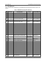
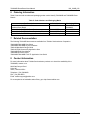
1
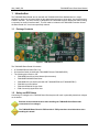
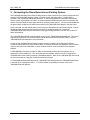
Simplifying System IntegrationTM
73M1966B
Demo Board User Manual
January 22, 2010
Rev. 1.2
UM_1966B_022
73M1966B Demo Board User Manual
UM_1966B_022
© 2008 Teridian Semiconductor Corporation. All rights reserved.
Teridian Semiconductor Corporation is a registered trademark of Teridian Semiconductor Corporation.
Windows is a registered trademark of Microsoft Corporation.
All other trademarks are the property of their respective owners.
Teridian Semiconductor Corporation makes no warranty for the use of its products, other than expressly
contained in the Company’s warranty detailed in the Teridian Semiconductor Corporation standard Terms
and Conditions. The company assumes no responsibility for any errors which may appear in this
document, reserves the right to change devices or specifications detailed herein at any time without
notice and does not make any commitment to update the information contained herein. Accordingly, the
reader is cautioned to verify that this document is current by comparing it to the latest version on
http://www.teridian.com or by checking with your sales representative.
Teridian Semiconductor Corp., 6440 Oak Canyon, Suite 100, Irvine, CA 92618
TEL (714) 508-8800, FAX (714) 508-8877, http://www.teridian.com
2
Rev. 1.2
UM_1966B_022
73M1966B Demo Board User Manual
Table of Contents
1
Introduction...................................................................................................................................... 5
1.1 Package Contents.................................................................................................................... 5
1.2 Safety and ESD Notes ............................................................................................................. 5
2
Connectors ...................................................................................................................................... 6
3
Connecting the Demo Board into an Existing System ....................................................................... 7
4
Connecting the Demo Board Directly to a PCM Test Set .................................................................. 8
5
73M1966B Demo Board Schematics, PCB Layouts and Bill of Materials .......................................... 9
5.1 Schematics .............................................................................................................................. 9
5.2 PCB Layouts .......................................................................................................................... 11
5.3 Bill of Materials ...................................................................................................................... 13
6
Ordering Information ...................................................................................................................... 14
7
Related Documentation ................................................................................................................. 14
8
Contact Information ....................................................................................................................... 14
Revision History .................................................................................................................................... 15
Rev. 1.2
3
73M1966B Demo Board User Manual
UM_1966B_022
Figures
Figure 1: 73M1966B Demo Board ........................................................................................................... 5
Figure 2: Connecting the 73M1966B Demo Board Directly to a PCM Test Set ......................................... 8
Figure 2 : 73M1966B 20-Pin TSSOP Demo Board Schematic Diagram Host Interface ............................. 9
Figure 3 : 73M1966B 20-Pin TSSOP Demo Board Schematic Diagram Line Interface ............................ 10
Figure 4: 73M1966B Demo Board Top Layer ......................................................................................... 11
Figure 5: 73M1966B Demo Board Bottom Layer .................................................................................... 11
Figure 6 : 73M1966B 20-Pin TSSOP Demo Board: Ground Plane Layer ................................................ 11
Figure 7 : 73M1966B 20-Pin TSSOP Demo Board: Power Plane Layer .................................................. 12
Tables
Table 2: J1 Pin Descriptions .................................................................................................................... 6
Table 3: J2 Pin Descriptions .................................................................................................................... 6
Table 4: J3 Pin Descriptions .................................................................................................................... 6
Table 1: 73M1966B Demo Board Bill of Materials .................................................................................. 13
Table 5: Order Numbers and Packaging Marks ...................................................................................... 14
4
Rev. 1.2
UM_1966B_022
73M1966B Demo Board User Manual
1 Introduction
The 73M1966B Demo Board can be used with the 73M1966/1866 Demo Motherboard or in target
applications where it is connected either by the appropriate connector or “blue wired” into the system that
is will be used with. The active circuitry is identical to the 73M1866B Keychain Board other than including
a connector for the GUI interface cable. The GUI cable is included in the 73M1966B Evaluation Kit and
the Demo Board kit if it has been specifically ordered.
1.1
Package Contents
Figure 1: 73M1966B Demo Board
The 73M1966B Demo Board Kit includes:
•
•
•
1.2
A 73M1966B Demo Board (Rev. D3)
GUI Interface Cable (included with 73M1966B-EVM and 73M1966B-DB-C)
The following documents on CD:
• 73M1966B Demo Board User Manual (this document)
• 73M1866B/73M1966B Data Sheet
• 73M1966B GUI User Guide (included with 73M1966B-EVM and 73M1966B-DB-C)
• 73M1966 Layout Guidelines
• 73M1x66 Worldwide Design Guide
• PCM Connectivity Application Note
Safety and ESD Notes
Connecting live voltages to the 73M1966 Demo Board system will result in potentially hazardous voltages
on the boards.
Extreme caution should be taken when handling the 73M1966B Demo Board after
connection to live voltages!
The 73M1966B Demo Board is ESD sensitive! ESD precautions should be taken when
handling this board!
Rev. 1.2
5
73M1966B Demo Board User Manual
UM_1966B_022
2 Connectors
This section describes the 73M1966B Demo Board connectors. All the digital signals and power supply
connections are made through a 20-pin header connector. The audio monitor is also brought out on this
connector. Table 1 describes the pins for the J1 connector. For convenience, most digital signals are
grouped with the PCM signals on the odd pins from pin 1 to pin 7, and the PCM CLKI pin is on pin 8. The
SPI signals can be found on the odd pins 9 through 17. Reset is on pin 19. The interrupt output is on pin
16. There are two power pins on pins 2 and 4 and two ground pins on pins 18 and 20. The audio monitor
output can be found on pin 10. There is also a CLKO pin that can be used for the rare case where the
73M1866B is used in the master mode.
Table 1: J1 Pin Descriptions
Pin
1
3
5
7
9
11
13
15
Pin Name
FSIO
DX
N/C
DR
CSB
SCLK
SDO
SDI
17
SDT
19
RSTB
Function
PCM Bidirectional Frame Sync
PCM Receive Digital Data Output
No Connect
PCM Transmit Digital Data Input
Chip Select - low true
SPI Clock
Serial Control Data Out
Serial Control Data In
Serial Data Thru – used in Daisy
Chain Mode
Reset - low true
Pin
2
4
6
8
10
12
14
16
Pin Name
VCC
VCC
CLKO
CLKI
AUDIO
N/C
N/C
INTB
3.3V power in
3.3V power in
PCM Highway Clock Output
PCM Highway Clock Input
Audio output for speaker
No Connect
No Connect
Interrupt Output - low true
18
GND
Ground
20
GND
Ground
Function
Table 2 describes the J2 connector pins. These are the bi-directional PSTN network connections that
pass the audio signals to and from the FXO.
Table 2: J2 Pin Descriptions
Pin
1
2
3
4
Name
N/C
TIP
RING
N/C
Function
No Connect
Bidirectional Analog Signaling
Bidirectional Analog Signaling
No Connect
The signals on the TIP and RING pins should also have a DC current that would normally come from the
PSTN. This current will usually be in the range of 20 to 100 mA, but typically about 40 mA. This current
is necessary for the FXO to operate normally. The FXO will not operate if the current drops below
approximately 13 mA.
Table 5 describes the J3 connector pins. J3 is used to connect a host PC to the Demo Board to provide
GUI control.
Table 3: J3 Pin Descriptions
Pin
1
3
5
7
9
6
Pin Name
SDI
SDO
SCLK
CSB
VCC
Function
Serial Control Data In
Serial Control Data Out
Serial Clock
Chip Select - low true
Pin
2
4
6
8
10
Pin Name
N/C
GND
GND
GND
N/C
Function
No Connect
No Connect
Rev. 1.2
UM_1966B_022
73M1966B Demo Board User Manual
3 Connecting the Demo Board into an Existing System
The 73M1966B Keychain Demo Board is designed to be easily connected to an existing system that has
access to a PCM and SPI interface. Table 1 provides the pin and signal names. Further detail is
provided in the 73M1866B/73M1966B Data Sheet. If connectivity between the Keychain Demo Board
and the system is provided by ‘blue-wire’, we recommend that 30 AWG wire be used as a minimum and
that the maximum length of these wires should not exceed 8 inches (20 cm). It is also recommended that
the ground have at least two 30 AWG wires connecting the 73M1966B Demo Board to the host board.
Once connected, the user should check for the integrity of appropriate clock and control signals. Ensure
the signals have minimal over-shoot and under-shoot on the signal transitions. Consult the
73M1866B/1966B Data Sheet for information on the signal timing and ensure the host SPI conforms to
these requirements.
The 73M1966B Demo Board is also designed to plug into the 73M1966B EVM Motherboard. This board
supports the connection of a PCM test device such as the Wandel and Goltermann PCM-4. See the
73M1966B-EVM User Manual for more information.
In order for the 73M1966B Demo Board to operate correctly it needs to be configured by software.
Teridian provided Reference Driver Software and Linux based Command Line application can be used to
configure and control the 73M1966B. Contact Teridian Sales for more information on the available
software.
If 73M1966B-DB-C has been provided, a cable is included that connects the GUI Interface J3 to a
Windows PC with a parallel port. This, along with the GUI software, will allow a user to configure the
73M1966B without the need to provide any embedded software. Refer to the 73M1966B GUI User Guide
for more information on using the Teridian provided GUI software.
If a 73M1966B Motherboard Evaluation Kit (73M1966B-EVM) is being used, the 73M1966B Demo Board
is inserted into the appropriate socket . For further details on operating this system, refer to the
73M1966B EVM User Manual.
Rev. 1.2
7
73M1966B Demo Board User Manual
UM_1966B_022
4 Connecting the Demo Board Directly to a PCM Test Set
The 73M1966B Demo Motherboard conveniently provides a power connector, a power switch, PCM
interface connectors, and clock connectors. However, it is not necessary to utilize the Motherboard when
evaluating the device set. In some applications, it might be better to directly connect the 73M1966B
Demo Board to the PCM channel test set. Even without the Motherboard, the 73M1966B can be used
with the GUI and a channel test set.
If only the 73M1966B Demo Board is used, the two-row J1 connector has all the necessary signals to
connect to the digital signals of the channel test set and 3.3 V power as shown in Figure 2. Other PCM
highway test sets should also require only the 73M1966B Demo Board to perform similar tests.
TO FRAME SYNC OUTPUT OF TEST SET
TO RECEIVE DATA INPUT OF TEST SET
J2
1
2
3
4
1
3
5
7
9
11
13
15
17
19
TO TRANSMIT DATA OUTPT OF TEST SET
CSB
SCLK
ANA
SDO
ANA
SDI
SDT
RSTB
2
4
6
8
10
12
14
16
18
20
VCC3.3
3.3V DC POWER INPUT
CLKO
TO TRANSMIT CLOCK OF TEST SET
AUDIO
INTB
GND
J1
J3
DIGITAL HEADER 10X2
ANALOG HEADER
2
4
6
8
10
1
3
5
7
9
SDI
SDO
SCLK
CSB
VCC3.3
GUI HEADER 5x2
Figure 2: Connecting the 73M1966B Demo Board Directly to a PCM Test Set
8
Rev. 1.2
73M1966B Demo Board User Manual
UM_1966B_022
5 73M1966B Demo Board Schematics, PCB Layouts and Bill of Materials
5.1
Schematics
J3
SDI
SDO
SCLK
CSB
VCC
0.1uF
C18
1
3
5
7
9
1nF
C19
FSIO
DX
1
3
5
DR
7
CSB
9
SCLK
11
SDO 13
SDI
15
SDT 17
RSTB 19
U5
2
4
6
8
10
GUI INTERFACE
VCC
2
4
6
8
10
12
14
16
18
20
CLKO
CLKI
AUDIO
C34
C47
1nF
10uF
INTB
J1
VCC
0.1uF
C30
1nF
DX
FSIO
CLKO
CLKI
+ C21
3.3uF
C17
AUDIO
1
2
3
4
5
6
7
8
9
10
SCLK
CS
INT
VPD
SDO
DR
SDI
DX
SDITHRU
FSIO
RST
PCLKO
PCLKI
VPT
PRP
VNPLL
PRM
AOUT
VNT
VPPLL
CONN SOCKET 10X2
20
19
18
17
16
15
14
13
12
11
INTB
PRP
PRM
TP20
VCC
73M1906-20
C33
1nF
0.1uF
C32
+ 3.3uF
TP19
1
2
1
2
VCC
C31
Figure 3 : 73M1966B 20-Pin TSSOP Demo Board Schematic Diagram Host Interface
Rev. 1.2
9
73M1966B Demo Board User Manual
UM_1966B_022
C1 0.022uF, 250V
R66
1M, 0805
NOTE: GND f or C35 and
C36 should be on the host
side of the barrier
C3 0.022uF, 250V
R68
1M, 0805
C35
R5 8.2, 1%, 0805
1
R58
240
PRM
T1
4
2
3
Pulse TFR
C10
0.22uF
C13
15pF
73M1916-20
C24
NC(1nF, 3KV)
C20
C9
1nF
0.22uF
C26
1nF
BR1
HD04
1 +
Q6
BCP-56
TRF600-150
- 2
E1
P3100SBRP
TB03100H
Q4
MMBTA92
3
1
1
2
3
4
C41
220pF, 630V
R2
10M, 0805
3
5.1K
3
R12
MMBTA42
1
Q3
L2
2 kOhm@100MHz
C36
220pF, 3KV
R3 412K, 1%
4 HEADER
C42
NC
2
PRP
1
20
19
18
17
16
15
14
13
12
11
R65 200
VBG1916
15pF
DCG
DCS
DCD
TXM
RXM
RXP
VPS
VNS
ACS
VBG
3
10uF
DCI
RGN
RGP
OFH
VNX
SCP
MID
VPX
SRE
SRB
J2
F1
2
1
C4
U6
1
2
3
4
5
6
7
8
9
10
Q7
MMBTA42
2
4 2
RGP
RGN
1
DCI
C14
L1
2 kOhm@100MHz
3
TP14
OFH
OHS
4
DCS
220pF, 3KV
C6
4.7uF
0.1uF
C48
R11
5.1K
R4
100K, 1%
17.4K, 1%
C49
100pF
3
R6
SRB 1
R8
2
SRE
21K, 1%
Q5
R9
52.3K, 1%
C7
ACS
MMBTA06
4.7uF
1
C37
0.01uF
C39
5600pF
C12
0.1uF
TP15
VPS
R10
174, 1%
D1
MMSZ475253BT1*
0.1uF
C38
C43
1nF
1
C8 +
4.7uF
TP18
VNS
VNS
* Optional, see layout design guide
Figure 4 : 73M1966B 20-Pin TSSOP Demo Board Schematic Diagram Line Interface
10
Rev. 1.2
73M1966B Demo Board User Manual
5.2
UM_1966B_022
PCB Layouts
Figure 5: 73M1966B Demo Board Top Layer
Figure 6: 73M1966B Demo Board Bottom Layer
Figure 7 : 73M1966B 20-Pin TSSOP Demo Board: Ground Plane Layer
Rev. 1.2
11
73M1966B Demo Board User Manual
UM_1966B_022
Figure 8 : 73M1966B 20-Pin TSSOP Demo Board: Power Plane Layer
12
Rev. 1.2
UM_1966B_022
5.3
73M1966B Demo Board User Manual
Bill of Materials
Table 4 provides the bill of materials for the 73M1966B Demo Board schematic provided in Figure 3 and
Figure 4.
Table 4: 73M1966B Demo Board Bill of Materials
Qty
Reference
1
2
2
3
2
HD04 rectifier bridge, 0.8A, 400V
0.022µF, 250V
10 µF
4.7μF 25V, X5R, 0805
0.22μF 16V, X7R, ceramic, 0603
Diodes Inc.
TDK
AVX, Panasonic
AVX, Panasonic
Panasonic
HD04-T
C3216X7R2E223K
TCP0J106M8RA
08053D475KAT2A
C0603C224K8RACTU
0.1μF 16V, X7R, ceramic, 0603
Panasonic, Kemet
C0603C104K8RACTU
15pF 50V, ceramic, 0603
Panasonic
ECJ-1VC1H150J
1nF 10V, X7R, ceramic, 0603
Panasonic
C0603C102K8RACTU
2
2
2
1
1
1
1
1
1
1
2
BR1
C1, C3
C4, C34
C6, C7, C8
C9, C10
C12, C17,C18,
C31, C38, C48
C13, C14
C19, C20, C26,
C30, C33, C43,
C47
C21, C32
C35, C36
C37, C39
C41
C49
E1
F1
J1
J2
J3
L1, L2
3.3μF 6.3V, tantalum, 0805
220pF, 3KV
0.01μF 50V, X7R, ceramic, 0603
220pF, 630V
100pF
P3100SBRP
TRF600-150
Header
Header
Header
2000 Ohm
TCP0J335M8R
C1812C102KHRACTU
06035C103KAT2A
C3216COG2J221J
ECJ-1CV1H101J
P3100SBLRP
TRF600-150
10 X 2
4X1
5X2
MPZ2012S601A
1
Q5
MMBTA06, NPN 80 V transistor SOT23
1
Q4
MMBTA92, PNP 300 V transistor SOT23
2
Q3, Q7
MMBTA42, NPN 300 V transistor SOT23
1
1
1
1
1
1
1
1
1
1
1
1
1
2
Q6
R2
R3
R4
R5
R6
R8
R9
R10
R11
R12
R58
R65
R66, R68
NPN 80 V transistor SOT223
10M, 5%, 1/8W resistor 0805
412K, 1%, 1/10W resistor 0603
100K, 1%, 1/10W resistor 0603
8.2, 5%, 1/8W resistor 0805
17.4K, 1%, 1/10W resistor 0603
52.3K, 1%, 1/10W resistor 0603
21K, 1%, 1/10W resistor 0603
174, 1%, 1/10W resistor 0603
3K, 5%, 1/10W resistor 0603
5.1 K, 5%, 1/10W resistor 0603
240, 5%, 1/10W resistor 0603
200, 5%, 1/10W resistor 0603
1 M, 5%, 1/8W resistor 0805
Rohm
Kemet
AVX, Panasonic
TDK
Panasonic
Teccor
Raychem
Sullins
Sullins
Sullins
TDK
Diodes, Fairchild,
Central, On Semi
Diodes, Fairchild,
Central, On Semi
Diodes, Fairchild,
Central, On Semi
Fairchild, On Semi
Yageo
Yageo
Yageo
Yageo
Yageo
Yageo
Yageo
Yageo
Yageo
Yageo
Yageo
Yageo
Yageo
1
T1
Pulse transformer
UMEC, Sumida,
Midcom
UBT0154, ESMIT
4180, 750110001
6
2
7
Rev. 1.2
Part Description
Source
Example MFR P/N
MMBTA06LT1G
MMBTA92LT1G
MMBTA42LT1G
BCP56
RC0805JR-0710ML
RC0603FR-07412KL
RC0603FR-07100KL
RC0805JR-078R2L
RC0603FR-0717K4L
RC0603FR-0752K3L
RC0603FR-0721KL
RC0603FR-07174RL
RC0603JR-073K0L
RC0603JR-075K1L
RC0603JR-07240RL
RC0603JR-07200RL
RC0603JR-071ML
13
73M1966B Demo Board User Manual
UM_1966B_022
6 Ordering Information
Table 5 lists the order numbers and packaging marks used to identify 73M1966B and 73M1866B Demo
Boards.
Table 5: Order Numbers and Packaging Marks
Part Description
73M1966B 20-Pin TSSOP Motherboard and
Standard Demo Board
73M1966B 20-Pin TSSOP Demo Board
73M1966B 20-Pin TSSOP Demo Board with GUI cable
73M1866B 20-Pin TSSOP Keychain Demo Board
Order Number
73M1966B-EVM
73M1966B-DB
73M1966B-DB-C
73M1866B-Keychain
Packaging Mark
73M1916-M
73M1906B
73M1966B-IM
73M1966B-IM
7 Related Documentation
The following 73M1x66B documents are available from Teridian Semiconductor Corporation:
73M1866B/73M1966B Data Sheet
73M1866B/73M1966B Layout Guidelines
73M1x66 Worldwide Design Guide
73M1x66 PCM Connectivity Application Note
73M1966B-EVM User Manual
73M1966B GUI User Guide
73M1866B/73M1966B FXOCTL Application User Guide
8 Contact Information
For more information about Teridian Semiconductor products or to check the availability of the
73M1966B, contact us at:
6440 Oak Canyon Road
Suite 100
Irvine, CA 92618-5201
Telephone: (714) 508-8800
FAX: (714) 508-8878
Email: [email protected]
For a complete list of worldwide sales offices, go to http://www.teridian.com.
14
Rev. 1.2
UM_1966B_022
73M1966B Demo Board User Manual
Revision History
Revision
1.0
1.1
Date
11/21/2008
9/14/2009
1.2
1/22/2010
Rev. 1.2
Description
First publication.
Added Section 4, Connecting the Demo Board Directly to a PCM Test Set.
Re-ordered sections.
In Figure 4, added a Zener diode to the schematic.
15