1
Simplifying System IntegrationTM
73M1822
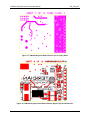
Keychain Demo Board User Manual
March 9, 2010
Rev. 5.0
UM_1822_007
73M1822 Keychain Demo Board User Manual
UM_1822_007
© 2010 Teridian Semiconductor Corporation. All rights reserved.
Teridian Semiconductor Corporation is a registered trademark of Teridian Semiconductor Corporation.
Simplifying System Integration is a trademark of Teridian Semiconductor Corporation.
MicroDAA is a registered trademark of Teridian Semiconductor Corporation.
Microsoft is a registered trademark of Microsoft Corporation.
Windows is a registered trademark of Microsoft Corporation.
All other trademarks are the property of their respective owners.
Teridian Semiconductor Corporation makes no warranty for the use of its products, other than expressly
contained in the Company’s warranty detailed in the Teridian Semiconductor Corporation standard Terms
and Conditions. The company assumes no responsibility for any errors which may appear in this
document, reserves the right to change devices or specifications detailed herein at any time without
notice and does not make any commitment to update the information contained herein. Accordingly, the
reader is cautioned to verify that this document is current by comparing it to the latest version on
http://www.teridian.com or by checking with your sales representative.
Teridian Semiconductor Corp., 6440 Oak Canyon, Suite 100, Irvine, CA 92618
TEL (714) 508-8800, FAX (714) 508-8877, http://www.teridian.com
2
Rev. 5.0
UM_1822_007
73M1822 Keychain Demo Board User Manual
Table of Contents
1
Introduction ................................................................................................................................... 5
1.1 Package Contents.................................................................................................................... 6
1.2 Safety and ESD Notes ............................................................................................................. 6
1.3 Demo Board Options................................................................................................................ 6
2
Connectors .................................................................................................................................... 7
3
Software Description ..................................................................................................................... 8
3.1 System Initialization ................................................................................................................. 8
3.2 73M1822 System Initialization .................................................................................................. 9
3.3 Off-Hook Procedure ............................................................................................................... 11
3.4 Dialing ................................................................................................................................... 12
3.4.1 DTMF Dialing .............................................................................................................. 12
3.4.2 Pulse Dialing............................................................................................................... 12
3.4.3 Adaptive Dialing .......................................................................................................... 14
3.5 LINE Sensing......................................................................................................................... 15
3.5.1 Line-In-Use (LIU) - Prior to the Modem Going Off-Hook............................................... 16
LIU Check Procedure............................................................................................................. 17
3.5.2 Parallel Pick Up (PPU) - While the Modem is Off-Hook................................................ 17
3.5.3 PPU Check Procedure ................................................................................................ 18
3.6 Ring Detect ............................................................................................................................ 18
3.6.1 Ring Detection Setup with Hardware Ring Qualifier ..................................................... 19
3.6.2 Ring Detection Using Coarse Ring Output................................................................... 20
3.7 Line Polarity Reversal Detection............................................................................................. 20
3.8 Line Snoop / Type I Caller ID Detection .................................................................................. 21
4
Demo Board Schematics, PCB Layouts and Bill of Materials ................................................... 24
4.1 Schematic .............................................................................................................................. 24
4.2 73M1822 MicroDAA Demo Board PCB Layout ....................................................................... 25
4.2.1 73M1822 42-Pin QFN Keychain Demo Board Layout .................................................. 25
4.2.2 Keychain Demo Board Physical Dimensions ............................................................... 27
4.3 Bill of Materials ...................................................................................................................... 28
4.4 Pin Descriptions ..................................................................................................................... 28
4.4.1 731822 Pinout............................................................................................................. 30
5
Related Documentation ............................................................................................................... 31
6
Contact Information..................................................................................................................... 31
Rev. 5.0
3
73M1822 Keychain Demo Board User Manual
UM_1822_007
Figures
Figure 1: MicroDAA System Block Diagram ............................................................................................. 5
Figure 2: 73M1822 Register Polling ......................................................................................................... 8
Figure 3: Off-Hook Procedure ................................................................................................................ 12
Figure 4: Pulse Dialing Sequence .......................................................................................................... 13
Figure 5: Dialing .................................................................................................................................... 14
Figure 6: Adaptive Dialing ...................................................................................................................... 15
Figure 7: Line-In-Use Detection ............................................................................................................. 16
Figure 8: On-Hook TIP-RING DC Reading ............................................................................................. 17
Figure 9: Parallel Phone Off-Hook Detection .......................................................................................... 18
Figure 10: Ring Qualifier ........................................................................................................................ 19
Figure 11: Ring Detector........................................................................................................................ 20
Figure 12: Line Polarity Reversal Detection............................................................................................ 20
Figure 13: Caller ID Detection Path........................................................................................................ 21
Figure 14: 73M1822 Keychain Demo Board Schematic.......................................................................... 24
Figure 15: 73M1822 Keychain Demo Board: Top Signal Layer and Silk Screen ..................................... 25
Figure 16: 73M1822 Keychain Demo Board: Layer 2, Ground Plane ...................................................... 25
Figure 17: 73M1822 Keychain Demo Board: Layer 3, Supply Plane ....................................................... 26
Figure 18: 73M1822 Keychain Demo Board: Bottom Signal Layer and Silk Screen ................................ 26
Figure 19: 73M1822 QFN 42-Pin Package: Pinout (top view) ................................................................. 30
Tables
Table 1: Host Interface JP2 Connector Pinout.......................................................................................... 7
Table 2: Line Interface JP1Connector Pinout ........................................................................................... 7
Table 3: 73M1822 Keychain Demo Board Bill of Materials ..................................................................... 28
Table 4: 73M1822 42-Pin QFN Package Pin Definitions......................................................................... 29
4
Rev. 5.0
UM_1822_007
73M1822 Keychain Demo Board User Manual
1 Introduction
The 73M1822 Keychain Demo Board integrates silicon Data
Access Arrangement (DAA) function along with Analog Front End
functions chipsets for worldwide compliance.
The 73M1822 MicroDAA is the world’s first single chip silicon DAA
IC that perform the advanced silicon Data Access Arrangement
(DAA) function along with Analog Front End functions.
The 73M1822 MicroDAA is available in a 42 pin QFN package for a
very small physical dimension and offers low cost global DAA
design.
H
O
S
T
GPIO
FS
FSD
SCLK
Line Interface
Circuitry
73M1822
Host Interface
Circuitry
I
SDIN
N SDOUT
T
M/S
E INT/RGDT
OSCIN
R
F OSCOUT
AOUT
A
C
E
RGP
RGN
OFH
DCI
DCD
DCB
DCE
TXN
RXM
RXP
SRE
ACS
SRB
L
I
N
E
I
N
T
E
R
F
A
C
E
PULSE
TRANSFORMER
73M1822
Figure 1: MicroDAA System Block Diagram
The 73M1822 performs a modem codec function that interfaces a Host/DSP and the PSTN (Public
Switched Telephone Network). The codec supports data rates up to V.92 with call progress signaling. In
addition to the codec function, the 73M1822 MicroDAA also performs other necessary DAA functions,
such as CID (caller identification), ring detection, tip/ring polarity reversal detection, on/off hook switch
control, pulse dialing, regulation of loop current (DC-IV), line impedance matching, line in use and parallel
pickup detection.
All data and control information between the LIC and the HIC is transferred across a low cost pulse
transformer barrier. Also all clock and synchronization information needed in LIC is embedded in this
data and control bit stream across the barrier transformer received from HIC and reconstructed within
LIC. The LIC interface to tip/ring of the PSTN significantly lowers the number of external components and
their cost.
The DAA feature integrated in this device offers a configurable US, TBR21, or other World Wide DAA
capability to the telephone line interface and an auxiliary DAC with gain control for line monitoring during
the call progress period.
Rev. 5.0
5
73M1822 Keychain Demo Board User Manual
1.1
UM_1822_007
Package Contents
The 73M1822 Keychain Demo Board Kit includes:
•
•
1.2
A 73M1822 Keychain Demo Board (Rev. D1)
The following documents on CD:
• 73M1822 Keychain Demo Board User Manual (this document)
• 73M1822/73M1922 Data Sheet
• 73M1822/73M1922 Schematic and Layout Guidelines
• 73M1x22 Worldwide Design Guide
Safety and ESD Notes
Connecting live voltages to the Demo Board system will result in potentially hazardous voltages on the
boards.
Extreme caution should be taken when handling the Demo Boards after connection to
live voltages!
The Demo Boards are ESD sensitive! ESD precautions should be taken when handling
these boards!
1.3
Demo Board Options
The 73M1822 Keychain Demo Board has 20-pin right angle connectors to plug on to a target DSP or
CPU system. Each has a 3.3 V power receptacle for powering on-board circuits from target system or
external power supply, or power can be supplied through the 20-pin connector along with the other
signals. The 73M1822 Keychain Demo Board allows the evaluation of the 73M1822 device for universal
modem, voice application and interface to a general DSP or CPU system use.
6
Rev. 5.0
UM_1822_007
73M1822 Keychain Demo Board User Manual
2 Connectors
Table 1 and Table 2 show all the connectors and jumpers available on 73M1822 Keychain Demo Board.
JP2 is the main connector for interfacing to a host processor or DSP board. JP1 is a connector for phone
line connection. Be aware that there is no high voltage and current protection circuit included in any
Keychain Demo Boards. Make sure these protection circuit components are placed in between the
telephone line and JP1 connector for a practical design. Line monitor/Call progress monitor speaker and
driver circuits are not available on the Keychain Demo Boards. Refer to the 73M1822 Keychain Demo
Board schematics for the protection circuit and Call Progress Monitor circuit references.
Table 1: Host Interface JP2 Connector Pinout
PIN Number
Name
Description
1
FSBD
Delayed FS
2
RINGD
Interrupt Output
3
VCC
3.3V Supply
4
RESET
Reset Input
5
AOUT
Call progress Monitor out
6
GND
Power Signal GND
7
FS
Frame Sync
8
SCLK
Serial Clock
9
AFEIN
Serial Data In
10
AFEOUT
Serial Data Out
Table 2: Line Interface JP1Connector Pinout
PIN Number
Rev. 5.0
Name
Description
1
TIP
Phone Line Connection
2
RING
Phone Line Connection
7
73M1822 Keychain Demo Board User Manual
UM_1822_007
3 Software Description
3.1
System Initialization
This section describes software that is not provided with the 73M1822 Keychain Demo Board but must be
provided by the Host system.
Once the system starts initialization, the system controller also needs to initialize the 73M1822 device set
as one of its peripheral. Some registers contain both control and status bits which are read only. When
using READ-MODIFY-WRITE to update an HIC register, care must be taken not to modify the status and
control bits unintentionally.
Upon power on reset, the HIC registers that contains the copy of the LIC registers (Register 0x12
to Register 0x1F) will be initialized to the default reset value. When the power of LIC is fed from
the HIC by setting the ENFEF bit (Register 0x0F Bit 7), LIC will be initialized with the default
register value that are identical to the values in register copy in LIC. Form this point, Any host
control to the LIC register bits by writing to an HIC register which is copy of the LIC register will
change both HIC and LIC maintaining images of each other unless data errors occur. In this
situation, there is a LIC register polling mechanism to regain this synchronization by host control.
Figure 2 illustrates how to re-synchronize the HIC and LIC registers by polling.
START
LIC ADD -> INDX3:0
(Reg19:3-0)
1-> POLL (Reg 19:7)
n
POLL(Reg19:7)=0?
y
MATCH(Reg19:6)=1?
y
Both HIC and LIC registers
specified by the ADD are
synchronized
Read POLLVAL(Register1F)
n
The HIC and LIC registers
specified by the ADD are
different
Error Handling
END
Figure 2: 73M1822 Register Polling
8
Rev. 5.0
UM_1822_007
3.2
73M1822 Keychain Demo Board User Manual
73M1822 System Initialization
The following example shows the sequence to bring the 73M1822 MicroDAA out of reset and to start up
after power up.
NOTE: The 73M1822 MicroDAA does not have a power on reset circuit. For proper operation, a reset
signal shall be asserted from the host by pulling the reset pin of 73M1822 low approximately for 100 ns or
longer after the power is stabilized. The 73M1822 device will be ready to use within 100 μs after the
removal of reset pulse from the reset pin.
Resetting the 73M1822
The 73M1822 package does not have a dedicated reset pin due to pin restriction. An alternative reset
can be asserted through the M/S pin (pin 21 of 73M1822 42-pin QFN).
Any low-to-high or high-to-low transition at this pin will result in internal reset block to initiate the reset
process. So if the MAFE needs to be in MASTER configuration, the host needs to generate an active low
reset signal as a reset signal at this pin. Use active high reset signal for SLAVE mode of MAFE
applications.
•
•
•
•
Power up the system.
Wait for 3.3V power to be stable
Pull M/S pin low for 100 ns then let it go high if the 73M1822 is in Master configuration. (Pull M/S pin
high for 100 ns or longer then let it go low in case of slave configuration)
Wait for 100 μs for PLL, OSC to be stabilized
Initializing MicroDAA
A. Frame Synchronization
•
•
•
RESET HC bit (Register 0x01 bit 0) in a frame sequence.
RESET HC bit (Register 0x01 bit 0) in next frame sequence.
Then the HIC is guaranteed to be in software controlled control frame mode, now. All the MAFE
serial data shall be data only unless host request by setting bit 0 of data.
B. Control Frame Generation
Software Controlled Control Frame
•
•
•
MASK CTL (TXD Bit 0) as 1 to request a subsequent control frame.
Write or read the 73M1822 HIC register using the MAFE control data format.
Make sure to MASK CTL (TXD bit 0) as 0 if the control frame is not needed.
Hardware Controlled Control Frame
•
•
•
MASK TXD Bit 0 as 1 to request a subsequent control frame.
SET HC bit (Register 0x01 bit0) using the MAFE control data format in the next frame.
From now on, there will be data and control frames alternating. Make sure not to miss this sequence.
Rev. 5.0
9
73M1822 Keychain Demo Board User Manual
UM_1822_007
C. 73M1822 HIC Initialize
•
•
•
•
•
•
Disable daisy chain by writing 00H to HIC Register 0x01.
Configure either Hardware control frame or software control frame by selecting the HC bit (Register
0x02:0).
Configure GPIOs by selecting GPIO Data (Register 0x03), GPIO Direction (Register 0x04), GPIO
Interrupt Enable (Register 0x05) and Interrupt Polarity (Register 0x06).
Timing Chain setup (Register 0x08 - - Register 0x0D). Register 0x0D value shall be written the last.
Any other writes to Register 0x08 to Register 0x0C are not really affecting to the PLL until Register
0x0D is being written. It is also recommended to set CHNGFS (Register 0x0D:3) bit in case further
sample rate changes are required for such as V.90 applications.
Enable Analog Front End blocks by setting ENFEH bit (Register 0x0F:7). And put device active by
clearing SLEEP bit (Register 0x0F:5).
Select system clock driven from PLL by setting FRCVCO bit of Register 0x0E bit 7. (The FRCVCO
bit shall be set at least 2 sample period after writing to Register 0x0D.)
D. LIC Init
73M1822 LIC initialization shall begin after the73M1822 LIC part is fully powered up and initialized. From
the HIC Initialization above, setting ENFE then the FRVCO bits will start powering the 73M1822 LIC.
From this moment, the Host shall wait for 100 to 200ms for the 73M1822 LIC to be ready.
•
•
•
•
•
Enable Front End functional blocks by setting ENFE bit (Register 0x12:2)
Write 0x01 to Register 0x18.
Select proper filter setting per each sample rate setting FSCTR bits (Register 0x16:3-0)
Select proper AC impedance termination by setting ACZ31,0 (Register 0x17: 4,3)
Enable receiver path by setting RXEN bit ( Register 0x16:6)
Example 1. Using Software Controlled Control Frame:
static const U16 init_afe_config[] =
// Must have Data(LSB=1), Control,
// Data(LSB=1), Control,.. FRAMES
{
REG02|0x00, REG02|0x00,
CTRL_FRAME, REG04|0x00,
CTRL_FRAME, REG03|0x00,
CTRL_FRAME, REG05|0x00,
CTRL_FRAME, REG06|0x00,
CTRL_FRAME, REG07|0x00,
CTRL_FRAME, REG08|AFE_CTRL08,
CTRL_FRAME, REG09|AFE_CTRL09,
CTRL_FRAME, REG0A|AFE_CTRL0A,
CTRL_FRAME, REG0B|AFE_CTRL0B,
CTRL_FRAME, REG0C|AFE_CTRL0C,
CTRL_FRAME, REG0D|AFE_CTRL0D,
CTRL_FRAME, RWB|REG03,
CTRL_FRAME, RWB|REG03,
GPIO
CTRL_FRAME, REG0F|0x8C
CTRL_FRAME, REG0E|0x80
// Force to Software controlled control frame (HC=0)
// GPIO 7,6,5,4 = outputs
// GPIO 7,6,5,4 output data =0000
// Timing chain set up (Smaple Rate)
// Delay for 2 sample cycle time to
// let PLL settle before Lockdet by dummy read
// Set ENFE Bit, Reset Sleep Bit
// Set FrVCO bit
};
note: CTRL_FRAME = 0x0001
10
Rev. 5.0
UM_1822_007
73M1822 Keychain Demo Board User Manual
Example 2. Using Automatic Control Frame (Hardware Controlled Control Frame):
static const U16 init_afe_config[] =
{
REG02|0x00, REG02|0x00,
CTRL_FRAME, REG02|HC,
0x0000, REG04|0x00,
0x0000, REG03|0x00,
0x0000, REG05|0x00,
0x0000, REG06|0x00,
0x0000, REG07|0x00,
0x0000, REG08|AFE_CTRL08,
0x0000, REG09|AFE_CTRL09,
0x0000, REG0A|AFE_CTRL0A,
0x0000, REG0B|AFE_CTRL0B,
0x0000, REG0C|AFE_CTRL0C,
0x0000, REG0D|AFE_CTRL0D,
0x0000, RWB|REG03,
0x0000, RWB|REG03,
0x0000, REG0F|0x8C
0x0000, REG0E|0x80
};
3.3
// MUST HAVE Dummy Data, Control, .. FRAMES
// Force to Software controlled control frame
// Enable Hardware controlled control frame
// GPIO Direction
// GPIO Data
// GPIO interrupt control
// GPIO
// Timing chain set up
// Dummy Data, Delay for 2 sample cycle time to
// let PLL settle before Lockdet by dummy read GPIO
// Set ENFE Bit, Reset Sleep Bit
// Set FrVCO bit
Off-Hook Procedure
Off-hook control in MicroDAA is different from that of a traditional DAA GPIO control mechanism. Due to
the communication delay between host and MAFE through the barrier interface, and possible error over
the channels, the Off-hook control of silicon DAA is quite complicated. The host controller needs to go
through many steps starting from initiating a Off-hook command by setting the OFH bit and waiting for the
status responses from the LIC and based on this status determine the next step to proceed.
The host controller has to manage all of the Normal On/Off hook sequence as shown in the following flow
chart in Figure 3.
Off-Hook Procedure
•
•
•
•
•
•
•
•
•
•
•
•
•
The MicroDAA system is in Barrier Power Mode. ( ENLPW bit (Register 0x02:2) =0)
Go off-hook by setting OFH (Register 0x12:7) to turn the DC path to the DCgm and Acgm and Shunt
regulator blocks.
Enable DCgm that provides appropriate DC current/voltage control to the line by setting ENDC
(Register 0x12: 6) bit.
Enable ACgm to provide a AC impedance matching to the line by setting ENAC (Register 0x12: 5) bit.
Enable Shunt loading ENSHL (Register 0x12:4) by writing 0xF6 to Register 0x12.
Wait for 3 ms.
Check if the voltage is too low by monitoring UVDET (Register 0x1E: 6) is set by interrupt or polling.
If there is no abnormality (UVDET=1) detected, then go to nominal mode by setting ENNOM bit
(Register 0x12:0) (Transition to NOMINAL Mode) Done/Ready
If the UVDET bit (Register 0x1E: 6) was set, then power down the Shunt Regulator by resetting
ENSHL (Register 0x12: 4).
Wait for 3 ms.
Check if UVDET (Register 0x1E: 6) is set by interrupt or polling.
If no abnormality detected, then go to nominal mode by setting EnNOM bit (Register 0x12:0)
(Transition to NOMINAL Mode) Done/Ready.
If there is an abnormality still, then determine the cause such as phone line is unplugged.
Rev. 5.0
11
73M1822 Keychain Demo Board User Manual
UM_1822_007
On Hook State
Mixed Mode
Go Off-hook?
No
AC,DC, Shunt Loading = Off
DLL, FSM, LSBI, BG = On
Disable UVDT INT (EnDT=0)
Disable EnNOM(=0)
Yes
Go Off-hook
OFH=1,EnDC=1
EnAC=1,EnShl=1
Wait 3ms
Enable DT INT (EnDT=1)
INT?
Yes
No
Disable DT INT (EnDT=0)
Shunt Loading
EnShl=0
*CP
EnShl=0
Wait 3ms
EnNOM =1;
Enter Nominal mode;
Enable DT INT(EnDT=1)
INT?
Ready
No
Yes
Disable DT INT (EnDT=0)
Continue to Seize the Line
NOTE: *CP for Call progres and dialing
Figure 3: Off-Hook Procedure
3.4
Dialing
3.4.1 DTMF Dialing
DTMF is considered to be a part of the modem signal. The DTMF signals can be generated by the host
DSP in a way similar to the other modem signals and transmitted to the line through a series of TBS data
frames sent from HIC to LIC. After the system going to off-hook, call progress monitoring and dialing can
be executed as shown in Figure 5.
3.4.2 Pulse Dialing
Pulse dialing can be performed by a host control. Figure 4 and Figure 5 show the control procedure of
pulse dialing with MicroDAA. A tone dialing can follow a normal off-hook procedure. An alternative offhook sequence is shown in Figure 6 with pulse dialing mode enabled. After dialing the last pulse digit,
and just before going to an on-line (data) mode, setting the ENLPW bit (Register 0x12: 2) would bring the
line power to the 73M1822 LIC. The ENNOM (Register 0x12:0) bit setting will end the Pulse dialing to get
into the normal data mode. There is delay from an OFH software bit control to actual out of the OFH
hardware pin due to the barrier interface.
12
Rev. 5.0
UM_1822_007
73M1822 Keychain Demo Board User Manual
PLDm (from Host)
Tone Dialing
Pulse Diagling Mode
Off-hook
OFH (REG12:B7)
On-hook
Off-hook
OFH (pin 2)
High BW
EnNOM
Low BW
2ms
EnLPW
LLM
Normal 2 Wire Mode
Figure 4: Pulse Dialing Sequence
Rev. 5.0
13
73M1822 Keychain Demo Board User Manual
UM_1822_007
*CP
Off-hook State
Dial tone detected
No
Pulse Dialing?
Yes
No
PLDm=1
PLDm=0
OFH=0
DTMF Tone on
Wait for break time period
Wait for On time
OFH=1
DTMF Tone off
Wait for make time period
Wait for Off time
Is Pulse digit done?
more digit to dial
Inter-digit
Delay
Yes
Yes
Yes
No
More digit to dial?
No
Done
Figure 5: Dialing
3.4.3 Adaptive Dialing
Adaptive dialing is a combination of DTMF and Pulse dialing. The MicroDAA system goes into an offhook condition without setting the EnNOM bit. First the dial tone detection is used to see if the line
supports DTMF by starting with DTMF dialing. After dialing the first digit using DTMF, if the dial tone
disappears, continue on tone dialing. If the dial tone is still present after sending a DTMF tone, the line
cannot support tone dialing so the system will dial in pulse mode from the first digit again. The host sets
the EnNOM bit after the dialing and call progress processing are done, but before the modem connection.
14
Rev. 5.0
UM_1822_007
73M1822 Keychain Demo Board User Manual
Off-hook State
Dial tone detected
Yes
PLDm=0
DTMF dial
Yes
Dial Tone exist?
No
PLDm=1
DTMF dial
PULSE dial
Done
Figure 6: Adaptive Dialing
3.5
LINE Sensing
For modems used in set-top boxes and fax applications, the modem lines are typically bridged onto the
same phone line that provides telephone service to the household. In this type of installation, the modem
is required to determine whether someone is using the shared phone line or not. There are two types of
shared phone line activity detection. While the target system (MicroDAA) is on-hook and the line is being
used by another device such as telephone, the target system should not go off-hook and interrupt the
other device. This feature is called line in use (LIU) detection. The other feature is called parallel pick-up
detection (PPU). While the target system is using the phone line (off-hook), if another device sharing the
same line goes off-hook, the target system should free up the line by going on-hook immediately and
releasing the line to the other device. In most cases the 73M1822-based product will have the lowest
priority. In cases where the product is an alarm, it may have the highest priority and other devices should
give up the line. The MicroDAA is capable of supporting this feature without additional external
components.
The line-sensing task is shared by HIC and LIC. The LIC, continuously, monitors the line with integrated
auxiliary A/D and sends the raw A/D measurement samples to the HIC over the barrier. The HIC
interprets this data for decisions under host control.
There are three user monitor outputs available from the auxiliary A/D: The first one is from RNG+/RNGoutput specifically designated for ring detection. The second one is from the DCI pin that monitors the Tip
and Ring line DC voltage for Line-In-Use (LIU) and Parallel Phone Pick-Up (PPU) detection. The last one
is from DCS pin monitoring the voltage drop across the Re to observe the DC current during off hook.
Rev. 5.0
15
73M1822 Keychain Demo Board User Manual
UM_1822_007
3.5.1 Line-In-Use (LIU) - Prior to the Modem Going Off-Hook
Before the modem goes to off-hook to occupy the phone line, modem needs to check whether the phone
line is already in use for a voice call. The timing of the modem’s off-hook transition can be delayed until
the modem determines that the phone line is available. Monitoring the TIP can do the LIU detection and
RING voltage indirectly by measuring the DV voltage at DCI pin with the Aux A/D integrated in 73M1822
LIC.
Both line in use (LIU) and parallel phone pick up (PPU) detection are required feature set of most
embedded modem applications that share the phone line with household phone. A line DC voltage
monitoring of the Tip and Ring before going off-hook enables detecting LIU, preventing human
conversation being disturbed by modem to go off-hook when someone else in the household is already
using the phone.
Monitoring the Tip and Ring voltage can also be used to indicate an extension pickup while off-hook. The
voltage will drop lower by the phone DC impedance (Rp) parallel to the MicroDAA DC resistance Rdaa,
indicating another extension has gone off-hook on the same line.
There are alternative methods to detect LIU and PPU, such as line energy detection. But the reliability
and qualification time required to detect these, the line voltage measurement method described here is
better than others and available at no cost with easier software implementation.
TELCO
MicroDAA
Rs
Vdaa
V
VBat
Parallel Phone
hook
Iphone
Rp
Figure 7: Line-In-Use Detection
As shown in Figure 7, the Vdaa measured by the MicroDAA will be Vbat while the MicroDAA is on–hook
condition and the parallel phone is on-hook, too. But the Vdaa will drop to a following level when the
parallel phone goes to off-hook stage.
Vdaa = Vbat * Rp / (Rs + Rp)
Where Rp = the Parallel phone DC resistance, Rs = DC Source resistance of Telco.
The following is a recommended procedure for LIU implementation.
16
Rev. 5.0
UM_1822_007
73M1822 Keychain Demo Board User Manual
LIU Check Procedure
•
•
•
•
•
•
•
73M1822 system is in barrier power mode ready to go Off-hook.
Read the AD converter sample from Register 0x1B. Then, calculate Tip/Ring voltage with
TRV=LV*11mV *101+1.4V.
Wait for 400 μs for Register 0x1B to be updated with new sample.
Read the AD converter sample from Register 0x1B. Then, calculate the TIP and Ring voltage.
Average these multiple TRV samples and compare with the LIU threshold value set. (i.e. 15 V).
If the TRV is lower than the threshold, then the Line is in use and do not go off-hook.
If the TRV is above the threshold and almost at 48V, then the line is idle to proceed to go off-hook.
Figure 8: On-Hook TIP-RING DC Reading
3.5.2 Parallel Pick Up (PPU) - While the Modem is Off-Hook
If the modem is off-hook and engaged in a data call, it is desirable for the modem to detect the off-hook
transition of the parallel phone and to immediately yield the phone line by going on-hook. Parallel phone
pickup sensing is done by measuring the Tip and Ring DC voltage changes resulted from the DC loading
changes to the line through the DCIN pin with the Aux A/D. As with Line-In-Use detection, the actual
determination on PPU is done by the host. The 73M1822 simply relays the activity on the line.
Rev. 5.0
17
73M1822 Keychain Demo Board User Manual
TELCO
UM_1822_007
MicroDAA™
Rs
VBat
off-hook
Vdaa
V
Idaa
Rdaa
Parallel Phone
hook
Iphone
Rp
Figure 9: Parallel Phone Off-Hook Detection
As shown in Figure 9, the Vdaa measured by the MicroDAA will be Vbat * Rdaa /(Rs + Rdaa) while the
MicroDAA is off–hook condition and the parallel phone is on-hook, too. But the Vdaa will drop lower to a
following level when the parallel phone goes to off-hook stage.
Vdaa = Vbat * (Rp//Rdaa) / (Rs + (Rp//Rdaa))
Where Rp = the Parallel phone DC resistance, Rdaa = MicroDAA DC resistance and Rs = DC Source
resistance of Telco.
3.5.3 PPU Check Procedure
•
•
•
•
•
•
•
•
3.6
73M1822 system is Off-hook in Data mode.
Measure the TRV voltage by reading Register 1B by TRV=LV*11mV *5+1.4V. Average the multiple
samples after the voltage settled down.
Save this value for as a 73M1822 off-hook voltage reference.
Periodically monitor the Tip and Ring DC voltage changes by reading the AD value from Register
0x1B and calculate the Tip and Ring voltage by TRV=LV*11mV *5+1.4V
If there is a significant voltage change occurring suddenly, take multiple samples with 400 μs intervals
for de-bouncing.
Compare the average of these multiple TRV samples with the stored off-hook voltage reference.
If the TRV is significantly lower than the reference off-hook voltage, then the parallel phone is offhooked and 73M1822 will go on-hook immediately if required.
If the TRV is nearly the same as the stored off-hook voltage, then the extension phone is not off
hooked. Then modem can stay on for off-hook.
Ring Detect
Ring detection is done through circuitry connected to LIC pins RGP+ and RGN-. Any possible voltage
transition will be a source for the “Wake up” signal to HIC. The 73M1822 then looks for a ringing
frequency (typically 20 Hz). The ring qualification is done in 73M1822 by validating both the amplitude
and frequency. The ring amplitude appears at RNG+ and RNG- pins is attenuated by 1/100 from the
value at tip and ring by external 1M ohm resistor and internal circuit. The actual ring voltage can be
calculated with the value of Aux A/D data appears in Rng7- Rng0 (Register 0x1A:7-0).
18
Rev. 5.0
UM_1822_007
73M1822 Keychain Demo Board User Manual
Both the Ring and Polarity Reversal Detection cases, the actual decision is made within 73M1822 by
qualifying the activities on the line against the amplitude and period threshold provided by the Host.
Typical ring signal is in a sine wave format between 16 Hz to 60 Hz. (Typically 20 Hz).
The amplitude varies by country specifications. There are countries require to detect the minimum levels,
and not to detect the maximum levels. The ring sensitivity can be controlled by setting the RGTH1,0 bits
in Register 0x0E.
A precision ring detection can be done by a CPU reading each ring samples appearing at Register 0x1A
and determine voltage and frequency of the ring. Note: 1LSB = 1.31/128 = ~10.23mV. Equivalent
voltage at Tip and Ring = 100 * 10.23mV =1.02V. Magnitude only. If this register value read is 0x34,
then the voltage at Aux A/D (Vad) is 0x34*10mv=52*10.23mV =532mV. The ring voltage at Tip and ring
is 100*Vad=53.2V.
Given these conditions, the proper method for measuring the Tip and Ring voltage is:
•
•
•
Input selection—Reset OFH bit
Read the AuxADC value from Register 0x1A
The 8-bit integer represents an ADC input voltage between 0 V and 263 V (full scale).
Qualification
Time
Threshold
time
Threshold
Figure 10: Ring Qualifier
3.6.1 Ring Detection Setup with Hardware Ring Qualifier
The ring qualifier output RGDT (Register 0x02:1) bit reflects the current status of ring. When this bit is
set, there is a valid ring signal present at the tip and ring pin. The host can monitor the output of the ring
qualifier by polling this bit periodically or by an interrupt by setting ENRGDT (Register 0x04:0) bit. The
ring qualifier examines the ring signal both by the ring amplitude which is set by Rgth1 and Rgth0 bits
(Register 0x0F:1-0) and by the ring frequency (time). The RGTH setting allows 3 different ring detection
threshold settings at 15V, 30V and 45V with 1/100 ring divider setting by the hardware.
Rev. 5.0
19
73M1822 Keychain Demo Board User Manual
UM_1822_007
RING
RING
TIP/
RING
T
RGDT
Figure 11: Ring Detector
3.6.2 Ring Detection Using Coarse Ring Output
The host CPU can run its own ring qualifier algorithm with the Rng7-0 samples. The Rng7-0 value
represents the voltage of ring samples at the moment. The host software shall handling all the voltage
and timing measurement. Host can take the ring signals up to every 400 μs which is the MicroDAA HIC
refresh rate on the Rng7-0 register.
3.7
Line Polarity Reversal Detection
The Polarity Reversal detection during on-hook is associated with caller ID protocols in Japan and some
European countries. In these countries, the caller ID signals are sent prior to the start of normal ringing.
A polarity reversal is used to indicate to the modem that transmission of caller ID information is about to
begin. The detection of a polarity reversal takes place while the modem is in the On-hook state. The
detection of on-hook polarity reversals is required for full compliance with the specified Caller ID protocols
in these countries. Polarity reversal detection is done at pins RG+ & RG- thru the Aux A/D. As described
earlier both this and Ring Detection cases, the actual decision is made within 73M1822 by qualifying the
activities on the line against the threshold provided by the Host.
Line Voltage
Qualification Time
>30msec
Threshold
ignore polarity reversal
in this band
time
Figure 12: Line Polarity Reversal Detection
Polarity Reversal Detection Procedure
Line polarity Reversal can be checked from the ring qualifier output RGDT (Register 0x02:1) bit. When
this bit is set, and if the RGDB is reset, then there is a LPR detected. The host can monitor RGDT by
polling this bit periodically or by an interrupt by setting ENRGDT (Register 0x04:0) bit.
20
Rev. 5.0
UM_1822_007
3.8
73M1822 Keychain Demo Board User Manual
Line Snoop / Type I Caller ID Detection
Line Snoop is for monitoring the signals such as DTMF, Speech, Tone or Caller ID carrier either from
local or the remote end appearing at TIP and RING terminals for system interacting with external devices
such as DTAM, Telephone set etc. The MicroDAA supports two snoop modes. One is through the RING
detector path and the other is RXP path. In case of using RXP path for snooping, there will be about
600 uA (48V/5K) current sinking from the phone line, which is small enough not to cause the line to go
off-hook. The Caller ID signal will be routed thru the normal path via Rxp pin and processed just as data.
Using the ring detector path does not draw any current for snooping. Through the ring detection path, an
optional 20 dB gain block can be activated to compensate the 20 dB loss inserted for ring detection.
There are three possible scenarios for detecting caller ID. Type 1 Caller ID (w/Snoop), Type II while
system in off-hook and Type II while the system is on hook but attached device is off-hooked. In all
cases, it is assumed that Caller ID is preceded by a trigger signal such as a Ringing, line Polarity
Reversal, or a CAS tone.
RNG+
RNG-
Ring
Detector
10K
10K
1M
1M
CID/100
CID
RingPath
20dB
Gain
Q4
OFH
10M
Vd
412K
Q3
Ring
DCI
73M1822 LIB/
73M1922
Tip
0.022u
0.022u Vd
CID
100K
TXM
RXM
CID
RXP
RxPath
Figure 13: Caller ID Detection Path
Caller ID Detection Scenario:
Type I caller ID while system On-Hook – Snoop Caller ID detection.
Type II caller ID is with the modem Off-Hook.
Type II with other parallel modem or Telephone device Off-Hook. – Snoop Caller ID detection.
Type I Caller ID Detection Procedure (Snoop via Ring Path)
MicroDAA system is On-hook in barrier power mode.
A valid ring, line polarity reversal or other trigger signaling is detected.
Enable receive path by setting RxEn bit (Register 0x16:6).
Reset SNPac bit of Register 0x 0x14:4 to disable snoop via signal path.
Reset Rxbst0 bit of Register 0x14:3.to restore ac path gain.
Set SNPm bit of Register 0x15:4 to enable ring path snoop.
Set Rxbst1 bit of Register 0x15:5 to add a 20 dB gain for CID.
Process the CID signals appears.
Reset SNPm bit of Register 0x15:4.
Reset Rxbst1 bit of Register0x 15:5.
Disable receive path by resetting RxEn bit (Register 0x16:6).
Rev. 5.0
21
73M1822 Keychain Demo Board User Manual
UM_1822_007
Type I Caller ID Detection Procedure (Snoop via Rx path)
MicroDAA system is on-hook by resetting OH bit. (Register 0x12:7)
A valid ring, line polarity reversal or other trigger signaling is detected
MicroDAA system goes to a low current off-hook ( =< 600 µA) state by setting OH bit only. (Register
0x12:7). Other bits such as ENDC,ENAC and ENSHL shall be turned off by resetting these bits.
Enable receive path by setting RxEn bit. (Register 0x16:6)
Reset SNPm bit of Register 0x15:4 to disable ring path snoop.
Reset Rxbst1 bit of Register 0x15:5 to disable ring path snoop.
Set SNPac bit of Register 0x14:4 to enable signal path snoop.
Set Rxbst0 bit of Register 0x14:3 to add additional gain for CID.
Process the CID signals appears.
Reset SNPac bit of Register 0x14:4 to disable snoop via signal path.
Reset Rxbst0 bit of Register0x14:3.to restore ac path gain.
Disable receive path by resetting RxEn bit (Register 0x16:6).
Type II Caller ID Snoop Procedure
MicroDAA system is on-hook.
Parallel phone off-hook detected (LIU)
Waiting for CID continuously by monitoring the line signal by snooping via ring path or Rx path until
the parallel phone goes back to on hook.
Call Progress/Line Monitoring
The call progress audio monitoring such as on-hook dialing can be implemented using the monitor DAC.
The 73M1822 HIC is with integrated DAC with independently programmable gain for TX and Rx signals.
An Audio power amplifier is required for driving loudspeakers. Since the gain can be adjusted with
CP_Mon Register (Register 0x10), level control in the speaker diver is not required. This analog output
can be used for following applications;
Call Progress Monitoring
Driving audio output for telephone line signals such as dial tone, dialing, ring back, busy tone
monitoring and modem signals through the speaker.
On-Hook Dialing
Same as call progress monitor.
Ringer Tone Output
Using the ring detector output status, Host DSP may generate ant tone or signal to the speaker by
transmit data stream.
Key Beep/System Alarm
Generating a beep or key tone is very useful for a certain types of keypad as a user input. The
availability of this feature is limited by while the modem is idle. While the modem is active, this
feature is not available.
Worldwide DAA Configuration
The 73M1822 offers a configurable global compliance with Line DC VI control, AC termination impedance
control and ring detection threshold adjustment features under software control. These parameters can
be set during the system initialization and can be change at any time when needed.
The AC Termination Impedance can be configured by selecting the ACZ(1:0) settings in Register
0x17:4-3.
The DC mask configuration is by selecting DCIV(1:0) settings in Register 0x13:7-6.
Ring detector threshold configuration is by selecting RGTH(1:0) in Register 0x0E:1-0. The precision
ring voltage sensing can be done by polling the ring signal samples read from the auxiliary ADC
from Register 0x1A. The host shall calculate the peak and frequency under software control.
22
Rev. 5.0
UM_1822_007
73M1822 Keychain Demo Board User Manual
The following example shows the LIC initialization using US impedance and DC mask setting.
static const U16 init_LIC_config[] =
{
CTRL_FRAME, (REG12<<8)|0x04,
CTRL_FRAME, (REG13<<8)|0x10,
CTRL_FRAME, (REG14<<8)|0x20,
CTRL_FRAME, (REG15<<8)|0x08,
CTRL_FRAME, (REG16<<8)|0xD0,
CTRL_FRAME, (REG17<<8)|0x00,
CTRL_FRAME, (REG18<<8)|0x01,
CTRL_FRAME, (REG19<<8)|0x81
// MUST HAVE Data, Control, Data, Control,.. FRAMES */
// Reset offhook control register. Register12=0x04, Set ENFE bit
// Register13=0x10, DCIV=00, ILM=0, THDCEN=1, PLDM=0,OVDTH=0,
// IDPD=0
// Register14=0x80, Set to 0db Gain in Tx path by DAA1,0=01
// Register 15=0x00
// Register16=0xD0, TXEN=1, RXEN=1, RLPNEN=0, ATEN=1,
// FSCTR(3:0) =0000
// Register17=0x00, ACZ(1:0)=00.
// Set Register18 =01
// Register19=81, POLL=1, INDX(3:0)=1.
};
Rev. 5.0
23
73M1822 Keychain Demo Board User Manual
UM_1822_007
4 Demo Board Schematics, PCB Layouts and Bill of Materials
4.1
Schematic
Figure 14 shows the schematic diagram of 73M1822 42-pin QFN Keychain Demo Board.
3
C37
0.01uF
C48
0.01uF
C7
1uF
R8
100K, 1%
1
+
2
MMBTA06
Q5
R6
100K, 1%
L1
VPS
C38
+ C8
0.1uF
4.7uF
C43
R67 1M
1nF
22
23
24
25
26
27
28
29
30
31
C19
2
27pF
27pF
C31
C32
+
C33
1nF
3.3uF
0.1uF
C25
FSBD
RINGD
VCC
RESET
AOUT
GND
FSB
SCLK
AFEIN
AFEOUT
JP1
1
2
R3
412K, 1%
HEADER 2
1nF
0.47uF
C10
0.47uF
R5
8.2
C49
+ C4
0.1uF
R11
3K
R4
100K, 1%
R52
200
C5
L2
2
3
T1
C14
15pF
2k Ohm@100MHz
100pF
C36
220pF, 3kV
VNS
10uF
4
C42
220pF, 300V
E1
P3100SBRP
R2
10M
Q3
U1
1
- 2
C9
C26
1nF
TRF600-150
5.1K
1
C24
NC (1nF, 3kV)
R18
Q2
MMBTA42
1K
1
NOTE: GND for C24, C35,
and C36 should be on the
host side of the barrier
Q6
3
1
2
3
4
5
6
7
8
9
10
HD04
2
1
R12
VNS
C13
15pF
JP2
F1
C35
220pF, 3kV
3
3
Q4
MMBTA92
MMBTA42 1
2 2
4
1
C18
73M1822
VND
FS
FSBD
SDOUT
SDIN
SCLK
INT
VPD
PRP
PRM
24.576MHz
M/S
VNM/VNT
VPA
AOUT
VNA
VNPLL
OSCOUT
OSCIN
VPD
VND
GPIO6
10
9
8
7
6
5
4
3
2
1
21
20
19
18
17
16
15
14
13
12
11
4
Y1
0.1uF
3
3.3uF
1nF
1 +
32
33
34
35
36
37
38
39
40
41
42
DCE
DCB
DCI
RGN
RGP
OFH
n/c
VND/VNX
SCP
MID
VPX
3
C15
2
C22
+
SRE
SRB
VBG
ACS
VNS
VPD/VPS
RXP
RXM
TXM
DCD
VCC
C28
C3
0.022uF (200V, 1206)
BR1
3
0.1uF
VNS
2k Ohm@100MHz
C1
0.022uF (200V, 1206)
R66 1M
C12
4
R10
255, 1%
R9
100K, 1%
BCP56
Isolation Barrier
HEADER 10
VCC
C17
C30
0.1uF
1nF
+ C21
3.3uF
Figure 14: 73M1822 Keychain Demo Board Schematic
24
Rev. 5.0
UM_1822_007
4.2
73M1822 Keychain Demo Board User Manual
73M1822 MicroDAA Demo Board PCB Layout
4.2.1 73M1822 42-Pin QFN Keychain Demo Board Layout
Figure 15: 73M1822 Keychain Demo Board: Top Signal Layer and Silk Screen
Figure 16: 73M1822 Keychain Demo Board: Layer 2, Ground Plane
Rev. 5.0
25
73M1822 Keychain Demo Board User Manual
UM_1822_007
Figure 17: 73M1822 Keychain Demo Board: Layer 3, Supply Plane
Figure 18: 73M1822 Keychain Demo Board: Bottom Signal Layer and Silk Screen
26
Rev. 5.0
UM_1822_007
73M1822 Keychain Demo Board User Manual
4.2.2 73M1822 Keychain Demo Board Physical Dimensions
PCB Dimensions
•
Size
•
Height with components and solder
1.54 x 1.27” (39.10 x 32.10 mm)
0.46” (11.75 mm)
Environmental
•
Operating Temperature
(function of crystal oscillator affected outside
• Storage Temperature
°-40 to +85°C
–10°C to +60°C)
-65 to 150°C
Power Supply
•
DC Input Voltage (powered from DC supply)
•
Supply Current
3.3 VDC ±10%
25 mA (off-hooked at room temperature) typical
Rev. 5.0
27
73M1822 Keychain Demo Board User Manual
4.3
UM_1822_007
Bill of Materials
Table 3: 73M1822 Keychain Demo Board Bill of Materials
Qty
Reference
Part
Digikey Pin
Manufacturer Pin
Manufacturer
1
2
1
1
1
1
2
BR1
C1,C3
C4
C5
C7
C8
C9,C10
HD04
HD04DICT-ND
HD04-T
DIODES Inc.
0.022uF, 250V 399-1242-1-ND
C1206C223K5RACTU
Kemet
10uF
399-3138-2-ND
C0805C106K9PACTU
Kemet
100pF
311-1069-1-ND
CC0603JRNP09BN101
Yageo
1uF
587-1241-1-ND
EMK107BJ105KA-TR
Taiyo Yuden
4.7uF
PCC2176CT-ND
ECJ-2FB0J475M
Panasonic
0.47uF
PCC1911CT-ND
ECJ-1VB0J474K
Panasonic
6
2
2
3
1
C12,C15,C17,C33,C38,
C49
0.1uF
C13,C14
15pF
C18,C19
27pF
C21,C22,C32
3.3uF
C24
NC
399-1095-1-ND
C0603C104K8RACTU
Kemet
445-1271-1-ND
C1608COG1H150J
TDK
PCC270ACVCT-ND
ECJ-1VC1H270J
Panasonic
PCC1925CT-ND
ECJ-2YB0J335K
Panasonic
PCC1772CT-ND
ECJ-1VB1H102K
Panasonic
445-2380-1-ND
C4532COG3F221K
TDK
478-1227-1-ND
06035C103KAT2A
AVX
445-2338-1-ND
C3216COG2J221J
TDK
P3100SBLRPCT-ND
P3100SBLRP
Teccor Electronics
TRF600-150-ND
TR600-150
Rachem
S1011E-36-ND
PBC36SAAN
Sullin
S1011E-36-ND
PBC36SAAN
Sullin
240-2396-1-ND
HZ0805C202R-10
Steward
863-MMBTA42LT1G
MMBTA42LT1G
ON Semi.
863-MMBTA92LT1G
MMBTA92LT1G
ON Semi.
863-MMBTA06LT1G
MMBTA06LT1G
ON Semi.
568-1639-1-ND
BCP56
Philips
541-10.0MCCT-ND
CRCW080510M0FKEA
Vishay
P412KHTR-ND
ERJ-3EKF4123V
Panasonic
P100KHCT-ND
ERJ-3EKF1003V
Panasonic
541-8.20CCT-ND
CRCW08058R20FNEA
Vishay
311-255HRCT-ND
RC0603FR-07255RL
Panasonic
311-3.0KHRCT-ND
RC0603FR-073KL
Yageo
311-5.10KHRCT-ND
RC0603FR-075K1L
Yageo
P1.00KHCT-ND
ERJ-3EKF1001V
Panasonic
P200HCT-ND
ERJ-3EKF2000V
Panasonic
311-1.00MCRCT-ND
RC0805FR-071ML
Yageo
NA
ESMIT-4180/750110001
Sumida//Midcom
NA
73M1822
Teridian
815-ABM8-24.576-B2-T
ABM8-24.576MHZ-B2-T
ABRACON
6
2
2
1
1
1
2
2
1
1
1
1
1
4
1
1
1
1
1
1
2
1
1
1
28
C25,C26,C28,C30,C31,
C43
1000pF
C35,C36
220pF, 3KV
C37,C48
0.01uF
C42
220pF, 630V
E1
P3100SBRP
F1
TRF600-150
J1
HEADER 2
J2
HEADER 10
L1,L2
2K Ohm
Q2,Q3
MMBTA42
Q4
MMBTA92
Q5
MMBTA06
Q6
BCP56
R2
10M
R3
412K, 1%
R4,R6,R8,R9
100K, 1%
R5
8.2, 1%
R10
255, 1%
R11
3K
R11,12
5.1K
R18
1K
R52
200
R66,R67
1M
T1
Pulse TFR
U1
73M1822
Y1
24.576MHz
Rev. 5.0
UM_1822_007
4.4
73M1822 Keychain Demo Board User Manual
Pin Descriptions
Table 4 shows the 73M1822 42-pin QFN package pin definitions.
Table 4: 73M1822 42-Pin QFN Package Pin Definitions
Pin
1
2
3
4
5
6
7
8
9
10
11
12
13
14
Rev. 5.0
Name
PRM
PRP
VPD/VPT
INT
SCLK
SDIN
SDOUT
FSD
FS
VND
GPIO6
VND
VPD/VPPLL
OSCIN
Pin
15
16
17
18
19
20
21
22
23
24
25
26
27
28
Name
OSCOUT
VNA/VNPLL
VNA
AOUT
VPA/VPM
VNM/VNT
M/S
SRE
SRB
VBG
ACS
VNS
VPS
RXP
Pin
29
30
31
32
33
34
35
36
37
38
39
40
41
42
Name
RXM
TXM
DCD
DCE
DCB
DCI
RGN
RGP
OFH
M20BP
VNX/VNS
SCP
MID
VPX
29
73M1822 Keychain Demo Board User Manual
UM_1822_007
4.4.1 731822 Pinout
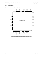
32 DCE
33 DCB
34 DCI
35 RGN
36 RGP
37 OFH
38 M20BP
39 VNX
40 SCP
41 MID
42 VPX
Figure 21 shows the 73M1822 42-pin QFN package pinout top view.
31 DCD
30 TXM
29 RXM
PRM 1
28 RXP
PRP 2
27 VPS
VPD/VPT 3
26 VNS
73M1822
INT 4
25 ACS
SCLK 5
24 VBG
SDIN 6
23 SRB
SDOUT 7
22 SRE
FSD 8
FS 9
M/S 21
VNA 20
VPA/VPM 19
AOUT 18
VNA 17
VNA/VNPLL 16
OSCOUT 15
OSCIN 14
VPD/VPPLL 13
VND 12
GPIO 11
VND 10
Figure 19: 73M1822 QFN 42-Pin Package: Pinout (top view)
30
Rev. 5.0
UM_1822_007
73M1822 Keychain Demo Board User Manual
5 Related Documentation
The following 73M1x22 documents are available from Teridian Semiconductor Corporation:
73M1822/73M1922 Data Sheet
73M1822 Keychain Demo Board User Manual (this document)
73M1822/73M1922 Layout Guidelines
73M1x22 Worldwide Design Guide
6 Contact Information
For more information about Teridian Semiconductor products or to check the availability of the 73M1822,
contact us at:
6440 Oak Canyon Road
Suite 100
Irvine, CA 92618-5201
Telephone: (714) 508-8800
FAX: (714) 508-8878
Email: [email protected]
For a complete list of worldwide sales offices, go to http://www.teridian.com.
Rev. 5.0
31
Mouser Electronics
Authorized Distributor
Click to View Pricing, Inventory, Delivery & Lifecycle Information:
Maxim Integrated:
73M1822-KEYCHN