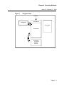
1
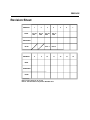
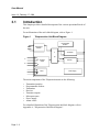
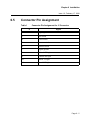
Positron Industries Inc.
User Manual
Positron Teleprotection™
Version 1.0
Model 8073
DOCUMENT CONTROL INFORMATION
Document Name:
Document ID:
Issue Number:
Document Part Number:
Revision Number:
Publication Date:
File Code:
Saved as Code:
User Manual
309
Issue 1.0
8073-24-03
4
February 17, 1998
48-52-61-65-185-309
e98bi001.fm
CONFIDENTIALITY NOTICE
The information contained in this document is the property of Positron Industries Inc. Except as
specifically authorized in writing by Positron Industries Inc., the holder of this document: 1) shall keep all
information contained herein confidential and shall protect same in whole or in part from the disclosure
and dissemination to all third parties, and 2) shall use same for operating and maintenance purposes only.
CUSTOMER SUPPORT
Should a problem arise, contact your customer support department. If the problem cannot be resolved by
your support department or if you have any questions, contact Positron’s Customer Support department at
1-800-361-2596.
© 1998 Positron Industries Inc.
Positron Teleprotection is a registered trademark of Positron Industries Inc.
Product names, other than Positron’s, mentioned herein may be trademarks and/or registered trademarks of
their respective companies.
DISCLAIMER NOTICE
Although Positron Industries Inc. has made every effort to ensure the accuracy of the information
contained herein, this document is subject to change without notice.
PREFACE
Revision Sheet
REVISION
1
2
3
DATE
Oct 26,
1987
Nov 6,
1989
July 26,
1996
4
5
6
7
12
13
14
Feb 17,
1998
APPROVED
NOTE
REVISION
8
9
Note 1
Note 2
10
11
DATE
APPROVED
NOTE
Note 1: Page 18, 42, 43, 46, 47, 49
Note 2: This document incorporates ECR #97-5277.
PREFACE
About This Manual
Welcome to the Positron Teleprotection™ User Manual. This manual provides a
detailed description of the hardware and software that make up the Teleprotection
unit.
The technical data contained in this manual are provided to assist the user in the
maintenance and troubleshooting of the unit.
This manual is organized as follows:
•
•
•
•
•
•
•
•
Chapter 1: Introduction
Chapter 2: Teleprotection Unit Operation
Chapter 3: Hardware Description
Chapter 4: Operating software
Chapter 5: Physical feature description
Chapter 6: Installation
Chapter 7: Technical Specifications
Appendix A: Teleprotection unit block diagram
PREFACE
Conventions
The following conventions are used throughout this manual.
Notes, Tips, Attentions, and Cautions
Notes are provided as background information that the user should know. Notes
are not critical to performing the procedure.
Tips are provided as additional information or hints on how the user can perform a
procedure.
Attentions are provided as information essential to the completion of a procedure.
Cautions are provided to advise users that failure to take or avoid a specified action
could result in loss of data or damage to the system.
The following is an example:
Note
It is recommended that the two solid state receiver outputs are connected in
series to avoid false tripping due to single point failure.
CONTENTS
Issue 1.0, February 17, 1998
Chapter 1
Introduction
1.1
Introduction . . . . . . . . . . . . . . . . . . . . . . . . . . . . . . . . . . . . . . . . . . . . . . . . . . . . . . . . . . . . . . . . . . . . . . . 1-2
1.2
Typical Setup . . . . . . . . . . . . . . . . . . . . . . . . . . . . . . . . . . . . . . . . . . . . . . . . . . . . . . . . . . . . . . . . . . . . . . 1-2
1.3
Synchronization and Combined Logic . . . . . . . . . . . . . . . . . . . . . . . . . . . . . . . . . . . . . . . . . . . . . . . . . . 1-4
1.4
Auxiliary Output Contacts. . . . . . . . . . . . . . . . . . . . . . . . . . . . . . . . . . . . . . . . . . . . . . . . . . . . . . . . . . . . 1-5
1.5
Internal Setting. . . . . . . . . . . . . . . . . . . . . . . . . . . . . . . . . . . . . . . . . . . . . . . . . . . . . . . . . . . . . . . . . . . . . 1-6
1.6
Function Map. . . . . . . . . . . . . . . . . . . . . . . . . . . . . . . . . . . . . . . . . . . . . . . . . . . . . . . . . . . . . . . . . . . . . . 1-7
Chapter 2
Teleprotection Unit Operation
2.1
Typical Operation . . . . . . . . . . . . . . . . . . . . . . . . . . . . . . . . . . . . . . . . . . . . . . . . . . . . . . . . . . . . . . . . . . 2-2
2.2
General Operation . . . . . . . . . . . . . . . . . . . . . . . . . . . . . . . . . . . . . . . . . . . . . . . . . . . . . . . . . . . . . . . . . . 2-3
Chapter 3
Hardware Description
3.1
Introduction . . . . . . . . . . . . . . . . . . . . . . . . . . . . . . . . . . . . . . . . . . . . . . . . . . . . . . . . . . . . . . . . . . . . . . . 3-2
3.2
Transmitter Interface . . . . . . . . . . . . . . . . . . . . . . . . . . . . . . . . . . . . . . . . . . . . . . . . . . . . . . . . . . . . . . . . 3-3
3.3
Programmable Dividers . . . . . . . . . . . . . . . . . . . . . . . . . . . . . . . . . . . . . . . . . . . . . . . . . . . . . . . . . . . . . . 3-3
3.4
Transmitter. . . . . . . . . . . . . . . . . . . . . . . . . . . . . . . . . . . . . . . . . . . . . . . . . . . . . . . . . . . . . . . . . . . . . . . . 3-4
3.5
Receiver . . . . . . . . . . . . . . . . . . . . . . . . . . . . . . . . . . . . . . . . . . . . . . . . . . . . . . . . . . . . . . . . . . . . . . . . . . 3-6
3.6
Amplitude Change Detector . . . . . . . . . . . . . . . . . . . . . . . . . . . . . . . . . . . . . . . . . . . . . . . . . . . . . . . . . . 3-10
3.7
Transistor Outputs . . . . . . . . . . . . . . . . . . . . . . . . . . . . . . . . . . . . . . . . . . . . . . . . . . . . . . . . . . . . . . . . . . 3-12
3.8
Microprocessors. . . . . . . . . . . . . . . . . . . . . . . . . . . . . . . . . . . . . . . . . . . . . . . . . . . . . . . . . . . . . . . . . . . . 3-13
3.9
Power Supply. . . . . . . . . . . . . . . . . . . . . . . . . . . . . . . . . . . . . . . . . . . . . . . . . . . . . . . . . . . . . . . . . . . . . . 3-14
Chapter 4
Operating Software
4.1
General Operation . . . . . . . . . . . . . . . . . . . . . . . . . . . . . . . . . . . . . . . . . . . . . . . . . . . . . . . . . . . . . . . . . . 4-2
4.2
Main program . . . . . . . . . . . . . . . . . . . . . . . . . . . . . . . . . . . . . . . . . . . . . . . . . . . . . . . . . . . . . . . . . . . . . 4-4
4.2.1
Initialization . . . . . . . . . . . . . . . . . . . . . . . . . . . . . . . . . . . . . . . . . . . . . . . . . . . . . . . . . . . . . . . 4-4
4.2.2
Background Tasks . . . . . . . . . . . . . . . . . . . . . . . . . . . . . . . . . . . . . . . . . . . . . . . . . . . . . . . . . . . 4-4
4.3
Foreground Tasks . . . . . . . . . . . . . . . . . . . . . . . . . . . . . . . . . . . . . . . . . . . . . . . . . . . . . . . . . . . . . . . . . . 4-5
4.4
Background . . . . . . . . . . . . . . . . . . . . . . . . . . . . . . . . . . . . . . . . . . . . . . . . . . . . . . . . . . . . . . . . . . . . . . .
4.4.1
Self-Checking . . . . . . . . . . . . . . . . . . . . . . . . . . . . . . . . . . . . . . . . . . . . . . . . . . . . . . . . . . . . . .
4.4.2
Transmission . . . . . . . . . . . . . . . . . . . . . . . . . . . . . . . . . . . . . . . . . . . . . . . . . . . . . . . . . . . . . . .
4.4.2.1
Synchronization . . . . . . . . . . . . . . . . . . . . . . . . . . . . . . . . . . . . . . . . . . . . . . . . . .
4.4.3
Reception. . . . . . . . . . . . . . . . . . . . . . . . . . . . . . . . . . . . . . . . . . . . . . . . . . . . . . . . . . . . . . . . . .
4.4.3.1
Combined Logic . . . . . . . . . . . . . . . . . . . . . . . . . . . . . . . . . . . . . . . . . . . . . . . . .
4.5
Sub-Routines . . . . . . . . . . . . . . . . . . . . . . . . . . . . . . . . . . . . . . . . . . . . . . . . . . . . . . . . . . . . . . . . . . . . . . 4-15
4-6
4-6
4-8
4-10
4-11
4-14
i
User Manual
Issue 1.0, February 17, 1998
4.5.1
4.5.2
4.5.3
4.5.4
4.5.5
4.6
Reference Level. . . . . . . . . . . . . . . . . . . . . . . . . . . . . . . . . . . . . . . . . . . . . . . . . . . . . . . . . . . . .
Current Frequency Level. . . . . . . . . . . . . . . . . . . . . . . . . . . . . . . . . . . . . . . . . . . . . . . . . . . . . .
White Noise Detection . . . . . . . . . . . . . . . . . . . . . . . . . . . . . . . . . . . . . . . . . . . . . . . . . . . . . . .
Local Test . . . . . . . . . . . . . . . . . . . . . . . . . . . . . . . . . . . . . . . . . . . . . . . . . . . . . . . . . . . . . . . . .
Remote Test. . . . . . . . . . . . . . . . . . . . . . . . . . . . . . . . . . . . . . . . . . . . . . . . . . . . . . . . . . . . . . . .
4-15
4-15
4-16
4-16
4-16
Difference Between Microprocessors “A” and “B” . . . . . . . . . . . . . . . . . . . . . . . . . . . . . . . . . . . . . . . . 4-17
4.6.1
State Diagram (Microprocessor “B”) . . . . . . . . . . . . . . . . . . . . . . . . . . . . . . . . . . . . . . . . . . . . 4-18
Chapter 5
Physical Feature Description
5.1
Front Panel. . . . . . . . . . . . . . . . . . . . . . . . . . . . . . . . . . . . . . . . . . . . . . . . . . . . . . . . . . . . . . . . . . . . . . . . 5-2
5.2
Rear Panel . . . . . . . . . . . . . . . . . . . . . . . . . . . . . . . . . . . . . . . . . . . . . . . . . . . . . . . . . . . . . . . . . . . . . . . . 5-3
5.3
Display. . . . . . . . . . . . . . . . . . . . . . . . . . . . . . . . . . . . . . . . . . . . . . . . . . . . . . . . . . . . . . . . . . . . . . . . . . . 5-4
5.4
Size . . . . . . . . . . . . . . . . . . . . . . . . . . . . . . . . . . . . . . . . . . . . . . . . . . . . . . . . . . . . . . . . . . . . . . . . . . . . . 5-6
5.5
Ventilation . . . . . . . . . . . . . . . . . . . . . . . . . . . . . . . . . . . . . . . . . . . . . . . . . . . . . . . . . . . . . . . . . . . . . . . . 5-6
5.6
Paint Finish . . . . . . . . . . . . . . . . . . . . . . . . . . . . . . . . . . . . . . . . . . . . . . . . . . . . . . . . . . . . . . . . . . . . . . . 5-6
Chapter 6
Installation
6.1
Installation Procedure . . . . . . . . . . . . . . . . . . . . . . . . . . . . . . . . . . . . . . . . . . . . . . . . . . . . . . . . . . . . . . . 6-2
6.2
Local Test . . . . . . . . . . . . . . . . . . . . . . . . . . . . . . . . . . . . . . . . . . . . . . . . . . . . . . . . . . . . . . . . . . . . . . . . 6-3
6.3
Remote Test . . . . . . . . . . . . . . . . . . . . . . . . . . . . . . . . . . . . . . . . . . . . . . . . . . . . . . . . . . . . . . . . . . . . . . . 6-3
6.4
Self-Check . . . . . . . . . . . . . . . . . . . . . . . . . . . . . . . . . . . . . . . . . . . . . . . . . . . . . . . . . . . . . . . . . . . . . . . . 6-4
6.4.1
Automatic Self-Check . . . . . . . . . . . . . . . . . . . . . . . . . . . . . . . . . . . . . . . . . . . . . . . . . . . . . . . . 6-4
6.4.2
Manual Self-Check . . . . . . . . . . . . . . . . . . . . . . . . . . . . . . . . . . . . . . . . . . . . . . . . . . . . . . . . . . 6-4
6.5
Connector Pin Assignment . . . . . . . . . . . . . . . . . . . . . . . . . . . . . . . . . . . . . . . . . . . . . . . . . . . . . . . . . . . 6-5
6.6
Setup Assignment . . . . . . . . . . . . . . . . . . . . . . . . . . . . . . . . . . . . . . . . . . . . . . . . . . . . . . . . . . . . . . . . . . 6-9
6.7
Test Points Assignment . . . . . . . . . . . . . . . . . . . . . . . . . . . . . . . . . . . . . . . . . . . . . . . . . . . . . . . . . . . . . . 6-11
Chapter 7
7.1
Technical Specifications . . . . . . . . . . . . . . . . . . . . . . . . . . . . . . . . . . . . . . . . . . . . . . . . . . . . . . . . . . . . . 7-2
Appendix A
ii
Technical Specifications
Teleprotection Unit Block Diagram
Chapter 1 Introduction
User Manual
Issue 1.0, February 17, 1998
e98bi002.fm
1.1
Introduction
1
Positron Teleprotection™ units are devices which have been designed to protect
networks from line faults. They operate with the help of a communication link that
joins two remote units together.
Under normal circumstances, the two units send each other a carrier that confirms
the presence of a telephone connection. When a fault (triggered by a trip contact
closure) is registered, the corresponding unit sends a trip signal to the other
extremity. The receiving unit capturing the message, activates its output to protect
the network.
1.2
Typical Setup
1
The Teleprotection unit consists of one transmitter and one receiver, both enclosed
in a single chassis. For an illustration of a typical Teleprotection setup, refer to
Figure 1.
Two units, located in separate locations, are joined together by an audio
communication link (4-wire), to form a full duplex tele-transmission system. Up to
five systems can share the same communication link, each of them using a separate
channel.
The transmitter modulates a frequency shift keying (FSK) signal upon detection of
a closure of a dry contact “trip input”. When the receiver detects a modulated FSK
signal, it closes its two solid state outputs. The two solid state outputs (pins 4,5,6
and 7), must be connected in series, to avoid a false trip caused by a single point
failure.
Page 1 - 2
Chapter 1 Introduction
Issue 1.0, February 17, 1998
Figure 1
Typical Setup: Teleprotection Units
POSITRON 8073
POSITRON 8073
TRIP
INPUT
14 +
26
TIP
TIP 24
7
6 + TO
TRANSMITTER
RECEIVER
RING
13
25
7
24 TIP
RING
MULTICONTACT
4 + RELAY
5
23
4-WIRE AUDIO LINK
TIP
26
+ 14
+ 6
TO
MULTICONTACT 5
RELAY
+ 4
RECEIVER
TRANSMITTER
23 RING
3
-
RING
25
2
3
+
-
POWER SUPPLY INPUT
TRIP
INPUT
13
2
+
POWER SUPPLY INPUT
Note
It is recommended that the two solid state receiver outputs are connected in
series to avoid false tripping due to single point failure.
Page 1 - 3
User Manual
Issue 1.0, February 17, 1998
1.3
Synchronization and Combined Logic
1
For improved security, two systems can be installed in parallel. In this mode, one
transmitter modulates its carrier output signal in opposite phase, and in
synchronization with the other transmitter. At the receiver end, the validation of a
trip command is accepted only if it is received on both receivers within a small
time interval (8 msec). For an illustration of synchronization and combined logic,
refer to Figure 2.
Figure 2
Synchronization and Combined Logic
Synchronization
Combined Logic
POSITRON 8073
14
26
TIP
TIP
POSITRON 8073
24
7
6
RECEIVER
TRANSMITTER
13
25
15
RING
RING
5
23
16 17 18
4
19
20
21 22
TO
MULTICONTACT
RELAY
TRIP
INPUT
17 18
15 16
14
21 22
26
TIP
19 20
TIP 24
7
6
RECEIVER
TRANSMITTER
13
25
POSITRON 8073
Page 1 - 4
RING
5
RING 23
4
POSITRON 8073
Chapter 1 Introduction
Issue 1.0, February 17, 1998
1.4
Auxiliary Output Contacts
1
The receiver has two sets of dry contacts:
•
•
A sequential event recorder contact which closes upon reception of a trip
signal
An alarm, form “C” contact. For a listing of the display codes, refer to Table 1
of Chapter 5, “Physical Feature Description”.
For an illustration of the auxiliary output contacts, refer to Figure 2.
Figure 3
Auxiliary Output Contacts
POSITRON 8073
8
9
RECEIVER
SEQUENCE OF EVENTS RECORDER (S.E.R.)
11
10
12
ALARM
(CONTACT POSITION SHOWN IN
UNPOWERED UNIT CONDITION)
Page 1 - 5
User Manual
Issue 1.0, February 17, 1998
1.5
Internal Setting
For in illustration of the internal setting for the Teleprotection unit, refer to Figure
4.
Figure 4
Internal Setting
REAR
SYNCHRONIZATION
J5
R163
OFF
LOOP BACK GAIN
ON
HIGH Z
RX
J8
COMBINED LOGIC
600 OHMS
OFF
J6
HIGH Z
ON
600 OHMS
FREQUENCY
1
0
1
LEVEL ADJUST
2
S4
TX
J7
3
TX
R205
4
POWER
ON
OFF
RX
R172
TP10 TP9
TP12 TP13
S1
S3
FRONT
To perform the internal setting
Page 1 - 6
1.
Connect the communication link.
2.
Match link impedance (J7 and J8 = 600 Ω)
3.
Select frequency (S4).
4.
Turn power ON.
5.
Adjust transmit level (R205) between TP12 and TP13.
6.
Adjust nominal level (R172) to obtain -10 dBm between TP9 and TP10 using
a non-selective dB meter in high impedance mode.
7.
Turn key to LOCAL TEST position.
Chapter 1 Introduction
Issue 1.0, February 17, 1998
8.
Adjust R163 to obtain -10 dBm between TP9 and TP10.
9.
Perform a LOCAL and a REMOTE TEST, then turn key to NORMAL. For
information concerning these tests, refer to Chapter 6, “Installation”.
10. Run a self-check. For information concerning the self-check, refer to Chapter
6, “Installation”.
11. After a few seconds, the front panel STATUS display should read 00.
1.6
Function Map
For an illustration of the Teleprotection unit function map, refer to Figure 5. For a
listing of the function locations, refer to Table 1.
Figure 5
Function Map
REAR
2
10
11
7
6
23
27
25
7
22
29
5
19
20
15
8
14
9
28
4
26
18
21
3
2
24
12
30
15
1
16
17
13
FRONT
SCALE: 1 cm: 2"
Note: The numbers in this diagram refer to the numbers found in the "Ref" column of the Function Locations table.
Page 1 - 7
User Manual
Issue 1.0, February 17, 1998
Table 1
Function Locations
Ref.
Page 1 - 8
Function
Location
Sheet
1
Two digit display driver
D1
1
2
Loop back relay drivers
C2
1
3
Surge protection
D1 . 5
1
4
Power supply
B1, B2
1
5
Power supply monitoring (U8)
D2
2
6
Watchdog for µP A and µP b (U9, U10)
D2
2
7
Alarm circuit (U11)
D1 . 5
2
8
Synchronization interface (U13)
D1
2
9
Combined logic interface (U14)
C1
2
10
Solid state output interface
A2, B2
2
11
Output leakage detector
A1, B1
2
12
Local oscillator low pass filter (U17)
D2
3
13
Analog multiplier (U21)
C2
3
14
Broadband bandpass filter (U23)
D2
3
15
I/F filter (U24, U25)
D1
3
16
Low pass TX filter (U19)
D2
3
17
TX line buffer (U27)
C1
3
18
RX signal level clipper (U29)
C1
3
19
60 Hz rejection filter (U29 small PCB)
A1 . 5
3
20
Out-of-band noise detector (small PCB)
A1
3
21
Fast level change detector (small PCB)
A2
3
22
Surge protection and loop back relay
A1
3
23
Programmable divider
A2 - D2
4
24
Trip input interface (U53, U55)
A1 - D1
4
Chapter 1 Introduction
Issue 1.0, February 17, 1998
Ref.
Function
Location
Sheet
25
Microprocessor “A” (U57)
A2 - D2
5
26
Microprocessor “B” (U70)
A1 - D1
5
27
Tick timer time base (1 msec)
D1 . 5
5
28
Local oscillator frequency check (U67)
C1 . 5
5
29
TX frequency check (U68)
B1 . 5
5
30
Receiver analog-to-digital converter
B2 - D2
6
Note: The numbers in the “Ref” column of this table refer to the numbers found
in Figure 5.
Note: Component reference designation number increases from sheet 1 to sheet
6. For example, U1 is located on sheet 1, U85 is located on sheet 6.
Page 1 - 9
Chapter 2 Teleprotection Unit
Operation
User Manual
Issue 1.0, February 17, 1998
e98bi003.fm
2.1
Typical Operation
2
For an illustration of the typical operation of Teleprotection units, refer to Figure 1.
Figure 1
Typical Operation: Teleprotection Units
TELEPHONE LINKS
E
R
Fn(C1)
C1
UNIT 1
UNIT 2
C2
Fn(C2)
Page 2 - 2
R
E
Chapter 2 Teleprotection Unit Operation
Issue 1.0, February 17, 1998
2.2
General Operation
Two Teleprotection units, located in different places, are joined together by a
communication link whose line status is monitored by a carrier. Each unit
continuously monitors a contact position originating from the protection relays.
When one of these contacts closes, the transmitter of the corresponding unit goes
into trip status. This status corresponds to the transmission of two frequencies
alternated every 25 msec. One of these frequencies corresponds to the one used for
monitoring the communication link. For an illustration of the transmission of these
frequencies, refer to Figure 2.
Figure 2
Frequency Transmission
25
50
75
t(msec.)
GUARD STATE
25
50
75
t(msec.)
TRIP STATE
The unit is designed to enable the connection of up to five units on one, four-wire
communication link.
For improved security, two units can be installed in parallel. As the units send each
other logic signals, parallel units must be synchronized before any instructions are
sent. Synchronization and combined logic block terminals, at the back of the unit,
are used for this purpose. Synchronization allows for the simultaneous
transmission of frequencies, and combined logic ensures the validity of received
messages. For an illustration of synchronization and combined logic, refer to
Figure 3.
A form C contact alarm output is accessible from the back of the unit.
Page 2 - 3
User Manual
Issue 1.0, February 17, 1998
Figure 3
Synchronization and Combined Logic
SYNCHRO
COMBINED LOGIC
Input
-
+
+
Output
-
Input
Input
Page 2 - 4
Input
Output
-
+
Output
-
COMBINED LOGIC
SYNCHRO
+
-
+
+
-
+
Output
-
+
-
Chapter 3 Hardware Description
User Manual
Issue 1.0, February 17, 1998
e98bi004.fm
3.1
Introduction
3
This chapter provides a detailed description of the various operational blocks of
the unit.
For an illustration of the unit’s block diagram, refer to Figure 1.
Figure 1
Teleprotection Unit Block Diagram
Programmable
Dividers
Transmission
Interface
2
Transmitter
µP
A
Transistor
Output
Receiver
B
Alarm
Power Supply
The main components of the Teleprotection unit are the following:
•
•
•
•
•
•
•
•
Transmitter interface
Programmable dividers
Transmitter
Receiver
Transistor outputs
Microprocessors
Power supply
Alarm circuit
For a detailed illustration of the Teleprotection unit block diagram, refer to
Appendix A, “Teleprotection Unit Block Diagram”.
Page 3 - 2
Chapter 3 Hardware Description
Issue 1.0, February 17, 1998
3.2
Transmitter Interface
The Teleprotection unit has two input interfaces connected to the trip contact
which allow for greater operational security. The contact closure must be validated
by two microprocessors before a trip order can be transmitted. The TB1-13 (J2-6)
and 14 (J2-5) input points, accepting a contact located in the protection relays, are
filtered by C8 and C9 to eliminate noise. The Teleprotection unit is electrically
isolated from the contact by opto-couplers (U53 and U55).
Each interface circuit is supplied with a low pass filter (relay from “A”
microprocessor trip contact), and K6 (relay from “B” microprocessor trip contact)
with an isolated +12 V power supply which allows for the simulation of a trip
during a self-check. These relays are activated by the “B” microprocessor for K5
and the by the “A” microprocessor for K6.
When the trip contact closes, a logic signal from the comparators (U54 and U56) is
passed on to the microprocessor. This condition triggers the transmitter and a trip
signal is sent.
3.3
Programmable Dividers
Besides generating transmission frequencies, the programmable dividers feed
various receiver circuits, for example the bandpass filter and the frequency
multiplier.
Programmable dividers are mainly made up of sheet registers (U50, U47, U44,
U41, U38, U35), programmable counters (U51, U48, U45, U42, U39, U36), fixed
dividers (U52, U49) for the receiver multiplier and for the transmitter, and JK
(U43, U40, U37) flip-flops for the receiver bandpass filters. The dividers are
programmed at the time of initialization.
By using the DIP switch which determines the selected frequencies, a serial signal
(via the microprocessor) is sent to the shift registers. The shift registers transmit
the signal in parallel, under microprocessor control. The programmable counters
detect the signal, decrement their value to zero and transmit a pulse to the fixed
dividers or JK flip-flops (÷2). The selected frequency is obtained at the output of
the fixed dividers.
Page 3 - 3
User Manual
Issue 1.0, February 17, 1998
3.4
Transmitter
The function of the transmitter is to send a guard frequency to check the status of
the communication link. When the trip contact closes, it then transmits a
modulation of the guard and trip frequencies (FM signal).
Depending on the positions of the three most significant bits in the DIP switch S4
(connected to the microprocessor), the programmable dividers will generate one of
the five available frequencies. The least significant bit of the DIP switch S4,
allows for the selection of a high frequency or a low frequency for the guard and
trip frequencies. For a listing of transmitter frequencies, refer to Table 1.
Before being routed to the communication link, the transmission signal,
originating from the programmable dividers, passes through a numeric switch
(U46). This switch allows microprocessor “A” to select the guard frequency or the
alternating trip frequencies.
The numeric switch output passes through a fixed divider (U49), followed by a
low pass filter (U19), whose role is to eliminate the third and subsequent
harmonics. This makes it possible to obtain a sine wave signal.
The output is then amplified by U27 and passed on to the T6 isolating transformer.
Potentiometer R205 provides a means for adjusting the transmission level. The
low pass output is also conditioned by U28, R203, R204, Q32 and R202 before
being routed to the microprocessor for purposes of frequency measurements.
During a self-check (fault detection), relay K2 (communication link relay) goes
into operation, looping the transmitter to the receiver. Potentiometer R163 makes it
possible to adjust the signal received to the nominal level.
Jumper J7 makes it possible to choose a 600 Ω impedance, or high impedance.
Warning
If the trip contact is connected in parallel with one or more units, do not
cross-connect. Connect similar points to each other. A bad connection will
immediately cause a trip signal.
Page 3 - 4
Chapter 3 Hardware Description
Issue 1.0, February 17, 1998
Table 1
Transmitter Frequencies
DIP Switch (S4)
Selector 4
Selector 3
Selector 2
Selector 1
Frequency (Hz)
0
0
1
0
1530 Low
frequency
0
1
0
0
1870 Low
frequency
0
1
1
0
2210 Low
frequency
1
0
0
0
2550 Low
frequency
1
0
1
0
2890 Low
frequency
0
0
1
1
1700 High
frequency
0
1
0
1
2040 High
frequency
0
1
1
1
2380 High
frequency
1
0
0
1
2720 High
frequency
1
0
1
1
3060 High
frequency
0
0
0
0
n/a
1
1
0
0
n/a
1
1
1
0
n/a
0
0
0
1
n/a
1
1
0
1
n/a
1
1
1
1
n/a
1 = open position
Page 3 - 5
User Manual
Issue 1.0, February 17, 1998
3.5
Receiver
The receiver uses the superheterodyne principle for improved selectivity when
capturing transmitted frequencies. The steps of the reception process are described
below:
Page 3 - 6
1.
The receiver input impedance must be adjusted to 600Ω resistive or high
impedance, using jumper J8. The signal received is isolated from the
Teleprotection unit by isolating transformer T5.
2.
The signal then passes through an amplitude clipper, thereby making it
possible to limit signal amplitude so as not to saturate the following stages.
3.
A high-pass filter eliminates 60 Hz noise.
4.
A variable gain amplifier (U30) is used to adjust the reception level at the
center of its dynamic range (i.e., -10dBm for input signals ranging from
-25dBm to 0dBm). The adjustment may be made by potentiometer R172.
5.
At this stage, an excessive level receiver signal (+22dB) is detected, and an
indication is sent to the microprocessor, after proper conditioning, via
hysteresis comparator (U31).
6.
When leaving amplifier U30, the signal is forwarded to bandpass U23
(switched capacitor filter), whose central frequency is determined by the
programmable dividers, thereby cutting off undesirable frequencies. The
bandwidth of this filter may be calculated as follows: bandwidth at -3dB,
Fh.Fb = .22 Fo. For a listing of the frequency of bandpass U23, refer to Table
2.
Chapter 3 Hardware Description
Issue 1.0, February 17, 1998
Table 2
Frequency of Bandpass U23
DIP Switch (S4)
Selector 4
Selector 3
Selector 2
Selector 1
Central
Frequency (Hz)
0
0
1
x
1615
0
1
0
x
1955
0
1
1
x
2295
1
0
0
x
2635
1
0
1
x
2975
x: non-significant
7.
A multiplier, U21, shifts frequencies received to 410Hz (low frequency) and
580Hz (high frequency), to take better advantage of the selectivity of filters
U24 and U25. The choice of frequencies of 410Hz and 580Hz is a
compromise between the reaction time of the bandpass filter and the rejection
of adjacent frequencies.
8.
The signal then passes into two very selective bandpass filters U24 and U25
(switched capacitor filter), whose function is to separate the trip frequency
from the guard frequency. These filters are quite selective due to their
reduced bandwidth, i.e.: bandwidth = Fh.Fb = .22 Fo (model 8073: 410Hz or
580Hz, model 8073A: 440Hz or 600Hz), where Fo has been shifted into the
lower frequencies by the multiplication of the received frequency and the
local oscillator.
9.
Analog/digital converter: each bandpass filter (U24-16 and U25-16) outputs
are then converted to digital values so that they may be read by the
microprocessors.
For an illustration of the analog/digital converter block diagram, refer to
Figure 2.
Page 3 - 7
User Manual
Issue 1.0, February 17, 1998
Figure 2
Analog/Digital Converter Block Diagram
SIGNAL
µPA
RECTIFIER
DEMODULATOR
A.M.
R
Q
S
Q
µPA
%
µPB
2
SLOPE
CLK (3 MHz)
10. The filter output passes through the rectifier and an A.M. demodulator. The
signal rectified in U78 is compared by U79 to a known slope. When the slope
reaches the level of the rectified signal, the U79 output changes status and
deactivates the SR flip-flop U69. The U69 flip-flop, in turn, deactivates the
slope generator by means of a switch (Q47 MOSFET). The flip-flop output
duration is proportional to the rectified voltage. It is converted to a burst of 3
Mhz pulses and drives circuit counters U63 and U64. For further information,
refer to Section 3.8, “Microprocessors”.
The conversion begins at every millisecond and lasts for a maximum of 0.9
milliseconds. For an illustration of the conversion period, refer to Figure 3.
Page 3 - 8
Chapter 3 Hardware Description
Issue 1.0, February 17, 1998
Figure 3
Representation of the Period
Rectified signal
Slope
t(msec.)
µPA
t(msec.)
Output from
SR flip-flop
t1
t2
t(msec.)
Page 3 - 9
User Manual
Issue 1.0, February 17, 1998
3.6
Amplitude Change Detector
The amplitude change detector permits the detection of excessive noise. The
method used consists of comparing the average level of a signal with its variation.
The signal originating from U30-7 is rectified by U32-2 and U32-6, and then it is
routed to two distinct points:
1. The peak detector and low pass U32-10 make it possible to obtain the average
level of the signal.
2. Differentiator U32-13 makes it possible to obtain signal variations.
These two signals are then compared by U33-3, thus producing an output signal
which will indicate the presence of an excessive level. For an illustration of the
circuit path, refer to Figure 4.
Page 3 - 10
Chapter 3 Hardware Description
Issue 1.0, February 17, 1998
Figure 4
Amplitude Change Detector
Input signal
Rectified (A, B)
filtered signal
Peak detector (D)
Dfferentiator (C)
Output signal
without noise (E)
Output signal
with noise (E)
Page 3 - 11
User Manual
Issue 1.0, February 17, 1998
3.7
Transistor Outputs
A protection circuit, made up of R86, Q17 and C54, checks system status and
protects it from certain faults by blocking the transistor outputs. For an illustration
of the transistor output, refer to Figure 5.
Figure 5
Transistor Outputs
µPA
Output A
Transistor output
Output B
Power failure
Watchdog
Leakage detector
The transistor outputs of the Teleprotection unit points TB2-6 and 7 (J2-20 and 19)
and TB3-4 and 5 (J2-18 and 17), are used to trigger the trip breakers. In the
NORMAL mode, relay K1 (transistor outputs relay) is connected to the protection
terminals. In the LOCAL and REMOTE modes, the relay is connected to the
leakage detection circuit.
The current leakage detector monitors the output transistor once a day, and
generates a warning alarm relay K3, and an appropriate code, to identify those
circuits having excess leakage.
The outputs are electrically isolated from one another, as well as from the rest of
the unit by means of transformers T3 and T4.
Diodes CR59 and CR48 protect the transistors from back E.M.F.
Attention
Outputs “A” and “B” must be connected in series to avoid false tripping on
a single point of failure.
Page 3 - 12
Chapter 3 Hardware Description
Issue 1.0, February 17, 1998
3.8
Microprocessors
Teleprotection unit operation is supported by two, 8085A, Intel 8-bit
microprocessors (U57 and U70). They operate independently from one another
while making unanimous decisions.
The clock output of microprocessor “A” (U57), oscillating at 3 Mhz, is divided by
3000 (U65 and U66) to produce a 1 Khz time base. This signal will serve to notify
the microprocessors by an interruption every millisecond (tick timer).
The demultiplexing of the address and data for the microprocessor is ensured by
latches U58 and U72. For each microprocessor, decoders U59 and U72 make it
possible to generate signals to the various peripheral circuits, from A12, A13 and
A14 address bits selected by the chip.
Each microprocessor comes with a watchdog timer (U9, U10) which, during a
power failure or software crash, resets the microprocessor to zero.
The unit’s operating software resides in 16 kilobytes of programmable ROM,
distributed over two, 2732 circuits of 4 kilobytes for the “A” microprocessor (U60,
U61) and two, 2732 circuits of 4 kilobytes for the “B” microprocessor (U73, U74).
The “A” microprocessor also has two, 8155 (U63 and U64) I/O circuits, each
integrating 256 bytes of RAM, a 3-port I/O, and a programmable binary counter.
The counters measure the A/D converter outputs by counting the total number of
pulses generated by these converters for each conversion. Communication with I/
O for microprocessor “A” consists mainly in controlling the various functional
blocks of the unit, such as: transmitter, receiver, A/D converter, front panel
controls and displays, frequency selection DIP switches, synchronization and
combined logic circuits.
The “B” microprocessor only requires one circuit (U77) for communication for its
I/O. It also checks local oscillator frequencies and transmission frequencies
programmed by the “A” microprocessor. This check consists of measuring, with
the binary counter operating at 3 Mhz (U76), the period duration of each of the
frequencies to be checked. The JK flip-flop circuits (U67 and U68), under
command of the “B” microprocessor, start and stop the corresponding counters
precisely at the beginning and end of the period to be measured.
Page 3 - 13
User Manual
Issue 1.0, February 17, 1998
3.9
Power Supply
A chopping power supply produces several outputs to meet the unit’s power
requirements. The different voltage outputs are the following:
1.
2.
3.
4.
12 V isolated (feeds the trip contacts)
8 V p-p (feeds transformers T3 and T4)
+5 V dc (mainly feeds the digital circuits)
+15 V dc (mainly feeds the analog circuits)
The input voltage, applied to points TB4-2 (positive point J3-1) and TB4-3
(negative point J3-3), is protected by the F1 and F2 two-amp fuses, type AGC 2A.
Diode CR34 serves as protection from back E.M.F. The power supply input filters
reduce the noise coming from the power supply through C32, C33, C34 and L3.
RLC components are provided to operate the oscillator at 20 KHz. This oscillator,
activated by T6, C29 and R36, feeds two power transistors Q13 and Q14, protected
by R35, R39 and R40 from transitory overcurrents. Two diodes, CR32 and CR33,
have been put between the emitter and the collector of each transistor to shortcircuit the back E.M.F. generated by the transistor change of status.
Then, the different voltage supplies are obtained either by means of the recitfying
filter and U3, U4 voltage regulators for the +5 V dc or U5, U6 for the ±15 V dc
respectively.
The percentage of error on voltage supplies may be read as follows:
•
•
•
•
Page 3 - 14
12 V unregulated
8 V unregulated
+5 V +4%
±15 V +4%
Chapter 4 Operating Software
User Manual
Issue 1.0, February 17, 1998
e98bi005.fm
4.1
General Operation
4
The Teleprotection unit software is contained in 16 kilobytes, distributed equally
between the two microprocessors. Two mutually checking microprocessors are
used for improved protection.
Because the software for the two microprocessors is practically identical, the
following descriptions will deal with microprocessor “A”. For information
concerning the differences between the two microprocessors, refer to Section 4.6,
“Difference Between Microprocessors “A” and “B””.
The Teleprotection software is made up of the following modules. For an
illustration of these modules, refer to Figure 1.
•
•
•
•
•
•
Page 4 - 2
Background tasks, making up the main program, turn in a closed loop, calling
up all jobs
Foreground tasks initiated by the interrupt sub-routine every millisecond
An interrupt sub-routine (INT7.5) ensures the link between background and
foreground tasks
Three multi-tasks: self-checking, transmission, reception
Several test sub-routines are called up by the main program
The macro-instructions simplifying the reading of the program are used in the
program
Chapter 4 Operating Software
Issue 1.0, February 17, 1998
Figure 1
Program Chart
POWER ON
INITIALIZATION
FOREGROUND
SUB-ROUTINE
INT75
BACKGROUND
MULTI-TASKS
Transmission
Reception
Self-check
Page 4 - 3
User Manual
Issue 1.0, February 17, 1998
e98bi005.fm
4.2
Main program
4
The main program, constituting background tasks, begins with an initialization
followed by a loop, composing the core of the program.
4.2.1
Initialization
The Teleprotection unit initialization is carried out after power has been turned on.
Initialization includes the following:
•
•
•
•
•
•
•
4.2.2
Initialization of I/O and counters
Initialization of the RAM
Programming of the dividers
Transmission of the channel number selected in the µPB
Authorization of the 7.5 interruption every millisecond
Display of the guard frequency status: high (1) and low (0) frequency on left
digit
Display of the channel number from 1 to 5, on right digit
Background Tasks
The start of background tasks follows initialization. These tasks include the
following:
•
•
•
•
•
•
•
•
•
•
•
•
•
•
Page 4 - 4
Check position of key, position of test button and activation of transistor relays
Check synchronization with the other unit
Reading input contact and trip transmission
Measure comparison level and check presence of white noise
Measure current level of frequencies
Check A/D converters’ absolute thresholds
Reading level of frequencies received and activation of outputs
Adjustment of time
Request remote test
Request local test
A self-check is performed every 24 hours except if a trip is present
Fault detection and blocks possible conduction of output transistors
End of background tasks
Set the watchdog to “0”
Chapter 4 Operating Software
Issue 1.0, February 17, 1998
4.3
Foreground Tasks
The INT7.5 sub-routine is called up at regular intervals, every millisecond, by a
signal originating in the microprocessor.
Every millisecond, the interrupt sub-routine executes the following foreground
tasks:
•
•
•
•
•
•
•
Reading the trip contact
Reading the level counters from the frequencies received from the A/D
converters
Re-initialization of the counters
Set the watchdog to 1
Update the timers
Update the quarter-second indicator
Start A/D converters by sending them a pulse
Page 4 - 5
User Manual
Issue 1.0, February 17, 1998
4.4
Background
4.4.1
Self-Checking
For an illustration of the self-checking state diagram, refer to Figure 2. For a listing
of the transitions between the different states, refer to Table 1.
Figure 2
Self-Checking State Diagram
1
Page 4 - 6
Transitory state, preparation of unit
2
Check relay status (K1) of output transistors
3
Stand-by for trip
4
Check memories
5
Check first transistor
6
Check second transistor and stand-by for loss of signal
Chapter 4 Operating Software
Issue 1.0, February 17, 1998
Table 1
Self-Checking State Transitions
State Transitions
Explanation
1-2
Start self-check
2-1
Fault signalled
2-2
Relay (K2) is connected
2-5
Relay (K2) is disconnected
3-1
Fault signalled
3-3
No trip, no transistor conduction
3-4
Trip, transistor conduction
4-1
Successful test or time expired or fault signalled
4-4
Transistor conduction
5-5
Leakage of first pair of transistors or time not
expired
5-6
First pair of transistors checked
6-1
Fault signalled
6-3
Second pair of transistors checked or loss of
signal
6-6
Leakage of second pair of transistors or time not
expired or no loss of signal
Page 4 - 7
User Manual
Issue 1.0, February 17, 1998
4.4.2
Transmission
For an illustration of the transmission state diagram, refer to Figure 3. For a listing
of the transitions between the different states, refer to Table 2.
Figure 3
Transmission State Diagram
1
Page 4 - 8
Transmission of guard frequency
2
Transmission of trip frequency for 25 msec
3
Transmission of guard frequency for 25 msec
Chapter 4 Operating Software
Issue 1.0, February 17, 1998
Table 2
Transmission State Transitions
State Transitions
Explanation
1-1
No request for transmission or fault or fault at
transmitter or no permission from µPB
1-2
Request for transmission and no fault at
transmitter and permission from µPB
2-1
No request for transmission or fault at
transmitter
2-2
Request for transmission and time not expired
and no fault at transmitter
2-3
Request for transmission and no fault at
transmitter and synchronization 1 toward 0, or
request for transmission and no fault at
transmitter and time expired
3-1
No request for transmission or fault at
transmitter
3-2
Request for transmission and no fault at
transmitter and synchronization 0 toward 1, or
request for transmission and no fault at
transmitter and time expired and permission
from µPB
3-3
Request for transmission and no fault at
transmitter and time not expired
Page 4 - 9
User Manual
Issue 1.0, February 17, 1998
4.4.2.1
Synchronization
When the signal is transmitted, synchronization makes it possible to obtain
simultaneous transmission of frequencies. The synchronization is included in the
transmitter sub-routine. A terminal at the rear of the unit is used to communicate
with another unit. When the unit transmits the trip frequency, depending on certain
conditions, it sends a synchronization signal to the other unit. When the other unit
receives the signal, it must conform with the synchronization signal and
synchronize itself with the fastest unit.
The synchronization is a 20 Hz frequency signal (50% duty cycle). For an
illustration of the synchronization effect, refer to Figure 4.
Figure 4
Example of the Synchronization Effect
FREQUENCY
(transmission)
Unit #1 trip
transmitter
(to t0) guard
t0
Unit #2
transmitter
(to t1)
t1
25msec
t(msec)
Unit #1
transmitter
(to t2)
Unit #2
transmitter
(to t0)
t2
t0
t(msec)
Page 4 - 10
Chapter 4 Operating Software
Issue 1.0, February 17, 1998
4.4.3
Reception
For an illustration of the reception state diagram, refer to Figure 5. For an
illustration of the reception thresholds, refer to Figure 6. For a listing of the
transitions between the different states, refer to Table 3.
Since noise influences wave forms, the criteria are narrowed in the presence of
noise. The criteria are:
•
•
•
•
•
Guard
Absence of two frequencies
Trip check
Trip
Recovery
Figure 5
Reception State Diagram
1
Guard
2
Absence of two frequencies
3
Trip check
4
Trip
5
Recovery
Page 4 - 11
User Manual
Issue 1.0, February 17, 1998
Figure 6
Reception Thresholds
5/4(+1.9dB)
3/2(+3.5dB)
LSURV
3/4(-2.5dB)
3/4(-2.5dB)
1/2(-6dB)
1/2(-6dB)
1/4(-12dB)
1/4(-12dB)
LTRIP
STATE #1
STATE #2
STATE #3
STATE #4
CONDUCTION
RECEPTION STATE 1, 2, 3, 4 AND 5
LSURV = Level of guard
LTRIP = Level of trip
Page 4 - 12
LOCK
STATE #5
Chapter 4 Operating Software
Issue 1.0, February 17, 1998
Table 3
Reception State Transitions
State Transitions
Explanation
1-1
Trip<1/4 and surv>3/4 and surv<5/4 and no
fault at receiver
1-2
Time expired and surv<3/4 and no fault at
receiver, or time expired and trip>1/4 and
surv<5/4 and no fault at receiver
1-5
If one of conditions of state 1 is false go to state
5
2-2
Surv<5/4 and trip<3/2 and time not expired and
no fault at receiver
2-3
Surv<1/4 and trip<3/2 and trip>3/4 and time not
expired and no fault at receiver
2-5
If one of conditions of state 2 is false go to state
5, or if phase and 1) surv high and surv<1/2 and
trip<1/2 and not locked 2) surv low and surv>1/
2 and trip>1/2 and not locked
3-3
If criteria for going to state 4 are false, on first
turn
3-4
Trip>3/4 and surv<1/4 and trip<3/2 and time
expired and no fault at receiver and combined
logic present
3-5
If one of conditions of state 3 is false or
combined logic absent on second turn
4-4
Serv<1/4 and trip>3/4 and trip<3/2 and no fault
at receiver and time not expired r
4-5
If one of conditions of state 4 is false go to state
5, or surv<1/4 and trip>3/4 and trip<3/2 and
time expired and no fault at receiver or if locked
5-1
Surv>3/4 and trip<1/4 and surv<5/4
5-5
If one of conditions in state 5 is false
Page 4 - 13
User Manual
Issue 1.0, February 17, 1998
4.4.3.1
Combined Logic
Upon reception, the combined logic ensures the validity of messages received. The
acceptance of a valid signal is permitted if the signal of the other unit comes within
the 8 msec gap. For an illustration of the combined logic signal, refer to Figure 7.
After three combined logic errors, the alarm is activated and code 38 is displayed.
To deactivate the alarm
1.
Set the key to LOCAL on both units
2.
Press TEST on both units
3.
If the combined logic test is successful, the combined logic error will be
deactivated.
Figure 7
Combined Logic Signal
20 msec.
30 msec.
INPUT
OUTPUT
8 msec.
Page 4 - 14
8 msec.
8 msec.
Chapter 4 Operating Software
Issue 1.0, February 17, 1998
4.5
Sub-Routines
4.5.1
Reference Level
This sub-routine makes it possible to obtain a reference level which will furnish a
means for comparing the present level of frequencies as well as for the detection of
white noise.
The reference level is calculated from the sum of guard (LSURV) and trip (LTRIP)
levels. This is done by taking 1/8 of the increase or decrease of the sum of the
level, i.e. LMSUM=LMSUM+1/8(SUM LMSUM). For an illustration of the
reference level, refer to Figure 8.
Figure 8
Reference Level (LMSUM)
SUM
LMSUM
t(msec.)
4.5.2
Current Frequency Level
This sub-routine, based on the level calculated in the Reference Level sub-routine,
makes it possible to check the status levels of the guard and trip frequencies. The
variable of this sub-routine, determining the level of comparison, will be used for
the acceptance of the change of state in the macro instructions of the reception.
Page 4 - 15
User Manual
Issue 1.0, February 17, 1998
4.5.3
White Noise Detection
By comparison levels, this sub-routine makes it possible to detect the presence of
white noise. The LMSUM reference level, calculated previously, is used to
compare the instant guard and tripping levels. In the presence of white noise, the
higher level criteria are narrowed, thereby allowing the obtaining of a hysteresis
level.
4.5.4
Local Test
The Local test makes it possible to check locally whether the trip and reception
circuits are operating properly by looping the transmitter to the receiver.
The sub-routine’s Key Positioning and Test Button provide access to the Local
test. The steps of the Local test are as follows:
•
•
•
•
•
•
4.5.5
Checks of the K2 relay (communication link relays) as well as checks of
possible transistor leakage are carried out once. To complete the test
successfully, the K2 line relay must be deactivated.
The TEST button must be pressed.
A trip order must be sent and received.
Checking of transistor conduction.
The display indicates 06: successful test.
This is the only way to unlock the combined logic error.
Remote Test
The Remote test makes it possible to check the link between the two units located
in two different places. Moreover, it ensures that a Remote test can only be
performed if a Local test has been previously carried out. The steps of the Remote
test are as follows:
•
•
Page 4 - 16
The Remote test may only be carried out if a Local test has been done first.
The checking of the relay is performed by a current sensor placed in series with
the relay coil.
Chapter 4 Operating Software
Issue 1.0, February 17, 1998
4.6
Difference Between Microprocessors “A”
and “B”
The main structure of the two microprocessors is mostly identical; however,
individual properties can be assigned to either of the microprocessors. For a listing
of the tasks that can be carried out by each microprocessor, refer to Table 4.
Table 4
Differences Between Microprocessor “A” and
Microprocessor “A”
Microprocessor Tasks
Microprocessor
“A”
Microprocessor
“B”
Initialization of I/O
X
X
Initialization of dividers
X
Read channel no
X
Display codes
X
Read input contact
X
Modulation of transmitter
X
Check transmitted frequency
X
X
Read level of frequencies received
X
X
Activation of output
X
X
Reset time
X
X
Start converters
X
Check synchronization and combined
logic
X
Page 4 - 17
User Manual
Issue 1.0, February 17, 1998
4.6.1
State Diagram (Microprocessor “B”)
The self-checking of microprocessor “A” and microprocessor “B” is identical. For
an illustration of the Transmission state diagram, refer to Figure 9. For a listing of
the transitions between the different states, refer to Table 5.
Figure 9
Table 5
Transmission State Diagram
1
Guard frequency transmission
2
Trip frequency transmission for 25 msec
3
Guard frequency transmission for 25 msec
Transmission State Transitions
State Transitions
Page 4 - 18
Explanation
1-1
No transmission request
1-2
Transmission request
2-1
Fault detection
2-2
25 msec time not expired
2-3
Trip frequency transmission for 25 msec
3-1
Fault detection or test successful
3-2
Guard frequency transmission for 25 msec
3-3
25 msec time not expired
Chapter 4 Operating Software
Issue 1.0, February 17, 1998
For an illustration of the Reception state diagram, refer to Figure 10. For a listing
of the transitions between the different states, refer to Table 6.
Figure 10
Reception State Diagram
1
Guard
2
Absence of two frequencies
3
Reception of trip frequency
4
Closure of protection contacts
5
Resynchronization (if guard absent)
6
Permission from other micro
Page 4 - 19
User Manual
Issue 1.0, February 17, 1998
Table 6
Reception State Transitions
State Transitions
Page 4 - 20
Explanation
1-1
Guard frequency present
1-2
Trip request
1-5
Fault detection
2-2
Absence of two frequencies
2-3
Trip received
2-5
Fault detection
3-3
Enables waiting for microprocessor “A”
3-5
Fault detection
3-6
Enables waiting for microprocessor “A”
6-4
Permission granted by other microprocessor
6-5
Fault detection
6-6
Waiting for permission by other microprocessor
4-4
Closure of protection contact
4-5
Normal trip or premature opening
5-1
Guard frequency present
5-5
Guard frequency absent
Chapter 5 Physical Feature
Description
User Manual
Issue 1.0, February 17, 1998
e98bi006.fm
5.1
Front Panel
5
For an illustration of the front panel, refer to Figure 1.
Figure 1
Front Panel
NORMAL
LOCAL TEST
REMOTE TEST
TX
RX
TELEPROTECTION
RX
TX
TEST
LINE
LINE
NOMINAL
-10 dBm
STATUS #
POSITRON #8073A
The front panel of the case includes the following:
•
•
•
•
•
A three position key switch: NORMAL, LOCAL and REMOTE. The key may
only be removed when in the NORMAL position.
A momentary TEST push-button
A numerical display made up of two digits, seven segments, complete with a
decimal point
Two warning signals constituted by electroluminescent diodes which indicate,
respectively, the presence of a trip order upon (TX) transmission and reception
levels of communication signals
Test points and adjustments for transmission and reception levels of
communication signals
Note
The model numbers for the Teleprotection unit are as follows:
•
•
8073: unit with old generation filters
8073A: unit with new generation filters
These units are identical with regards to performance and characteristics
and are interchangeable.
Page 5 - 2
Chapter 5 Physical Feature Description
Issue 1.0, February 17, 1998
5.2
Rear Panel
5
For an illustration of the rear panel, refer to Figure 2.
Figure 2
Rear Panel
1 2 3
4 5
6 7
-
-
-
129 V dc
or 48 V dc
TRIP A TRIP B
OUTPUT
8 9 10 11 121314 15 16 1718 1920 21 22 23242526
O CN N
T
U
R
O O
T
I
ALARM
P
P
U
I
T
N
S
P
T
U
A
T
T
U
S CONTACT
I
N
P
U
T
-
-
-
O
U
T
P
U
T
I
N
P
U
T
O
U
T
P
U
T
SYNC. COMB.
RX TX
GND
LINE
The rear panel of the case contains type Weidmüller transversal terminals, model
AKA 2.5, grouped separately.
Page 5 - 3
User Manual
Issue 1.0, February 17, 1998
5.3
Display
5
The display is made up of two modules with seven segments (U1, U2, DS1, DS2).
It displays codes indicating the different statuses of the Teleprotection unit. For a
listing of the display codes, refer to Table 1.
Table 1
Display Codes (software Vx.9)
Alarm Relay
Code
Page 5 - 4
Description
A
D
L
I
00
No code displayed (normal)
02
Self-check delayed (trip command in
progress)
03
Self-check halted (key not in normal
position)
04
Key in REMOTE TEST position
I
05
Key in LOCAL TEST position
I
06
LOCAL TEST (successful)
I
08
Key at REMOTE TEST without having
performed a LOCAL TEST first
I
09
Self-check in less than a minute
11
Fault detected by µPB
12
Leakage of xtor Q29 (LOCAL TEST)
L
I
13
Leakage of xtor Q30 (LOCAL TEST)
L
I
14
Non-conducting output (LOCAL TEST)
L
I
15
Continuous SPACE frequency without
MARK-SPACE-MARK-...modulation
16
Too strong received In Band signal
A
D
17
Carrier lost
A
D
18
Out-of-band noise (detected by
hardware)
A
D
19
Excessive In Band noise
A
D
A
D
R
Chapter 5 Physical Feature Description
Issue 1.0, February 17, 1998
Alarm Relay
Code
Description
A
D
L
21
Invalidated trip
25
Hardware fault during self-check
26
Defective ROM memory
A
L
27
Defective RAM memory
A
L
31
Unsuccessful reconnection of line during
a LOCAL test (loop back)
33
Unsuccessful reconnection of telephone
line
38
Combined logic error
40
Invalid channel at power up
88
Watchdog error
A
D
8.8.
Defective power supply
A
D
Legend
The alarm relay is activated:
•
•
•
•
•
L
L
A
I
R
I
I
D
R
A = after three seconds of continuous fault
D = duration of the fault
L = locked until manual or automatic self-check
I = immediately for the duration of this status error
R = reset the unit by turning the unit OFF then ON
Page 5 - 5
User Manual
Issue 1.0, February 17, 1998
5.4
Size
•
•
•
5.5
Width: 482 mm (19”)
Height: 88.1 mm (2 modular units, 3-1/2”)
Depth: 335 mm (14”, including connectors)
Ventilation
On the top panel, two air vents ensure ventilation by natural convection within the
unit. One UM (1-3/4”) spacing is recommended between units.
5.6
Paint Finish
The case has a clear, green, glossy finish, in compliance with standard SN-61.2.
Page 5 - 6
Chapter 6 Installation
User Manual
Issue 1.0, February 17, 1998
e98bi007.fm
6.1
Installation Procedure
6
To install the Teleprotection unit, follow the steps below and then use the
following sections to preform various tests. For an illustration of the front and rear
panels of the Teleprotection unit’s case, refer to Chapter 5, “Physical Feature
Description”. For an illustration of the locations of the test points, refer to Section
6.7, “Test Points Assignment”.
To install a Teleprotection unit
1.
Check that jumpers J7 and J8 are in the proper positions: 600 Ω or high
impedance.
2.
Using S4 inside the unit, adjust the desired channel. For further information
about S4 settings, refer to Table 5.
3.
Using S1 inside the unit, turn it on (i.e., the ON/OFF switch to the ON
position). The unit will run a self-check instantly.
4.
Upon power up, the display will indicate momentarily the unit channel
number: high frequency=1 or low frequency=0, as well as the channel
number (from 1 to 5).
5.
Set the key to the NORMAL position.
6.
Adjust transmission level on the line (0 to -25 dBm) using transmission
potentiometer R205, located on the front panel.
7.
Adjust the nominal level (-10 dBm) using potentiometer R172, located on the
front panel.
8.
Set the key to the LOCAL position and adjust R163 to obtain the nominal
level (-10 dBm).
9.
Perform a LOCAL test.
10. Perform a REMOTE test.
11. Set the key to the NORMAL position.
12. Run a SELF-CHECK, refer to Section 6.4.2, “Manual Self-Check”.
Page 6 - 2
Chapter 6 Installation
Issue 1.0, February 17, 1998
6.2
Local Test
6
The purpose of the local test is to ensure the proper operation of the transmission
and reception circuits.
To perform a Local test
6.3
1.
Set the three-position key switch to LOCAL. The display should show 05.
2.
Depress the TEST push-button. Trip indicators TX and RX should light up.
The display should show 06.
Remote Test
The purpose of the remote test is to ensure the proper operation of the
communication link between the two units. The remote test may only be
performed once the local test has taken place.
To perform a Remote test
1.
Set the switch to LOCAL.
2.
Press the TEST push-button.
3.
Set the switch to REMOTE. The display should show 04 indicating that the
REMOTE test may now be executed.
4.
Press the TEST push-button of one unit. Check that TX lights up on the
transmitting unit and that RX lights up on the receiving unit.
5.
Repeat for the other Teleprotection unit.
Page 6 - 3
User Manual
Issue 1.0, February 17, 1998
6.4
Self-Check
If a transistor leakage of the pair read by “B” is detected, and a self-check is
requested, only code 11 will be displayed. For further information regarding
display codes refer to Table 1 of Chapter 5, “Physical Feature Description”.
6.4.1
Automatic Self-Check
The unit performs a self-check, once a day, by isolating itself from the
communication link and protection circuits using the receiver and transmitter
interconnection. This procedure is controlled by the microprocessors.
Time Adjustment
The time adjustment, when the next self-check will be performed, is set with the
S3 button located inside the unit. Using the display to determine corresponding
time, pressing the button will determine the number of hours the next self-check
will occur.
6.4.2
Manual Self-Check
The operation of this function may be checked by triggering a self-check manually.
Instant Manual Check
While pressing the TEST push-button, press the S3 push-button. The self-check is
initiated instantly and the TX and RX lights will light up momentarily.
Manual Check with Delay
A self-check with a one-minute delay may be performed. Using the S3 push-button
inside the unit, reduce the number of hours which remain for the self-check to
zero. Release the S3 push-button. Code 09 will appear on the display. Wait for one
minute, the TX and RX lights will light up to indicate that the self-check has been
initiated.
Page 6 - 4
Chapter 6 Installation
Issue 1.0, February 17, 1998
6.5
Connector Pin Assignment
Table 1
Connector Pin Assignment for J1 Connector
J1
Signal
1
Digital ground
3
Test button
4
Local switch
5
Remote switch
6
Normal switch
7
Digital ground
8
Cathode TX light
9
Cathode RX light
10
Anode TX light
11
Anode RX light
Page 6 - 5
User Manual
Issue 1.0, February 17, 1998
Table 2
Connector Pin Assignment for J2 Connector
J2
Page 6 - 6
TB
Signal
1
15
Synchronization input +
3
19
Combined logic input +
6
14
Trip supply +
5
13
Trip input
4
8
Ser relay
7
16
Synchronization input -
8
9
Ser relay
9
17
Synchronization output +
10
18
Synchronization output -
11
10
Common alarm
12
20
Combined logic input -
13
21
Combined logic output +
14
12
Alarm normally closed
15
22
Combined logic output -
16
11
Alarm normally open
17
5
- A transistor output
18
4
+ A transistor output
19
7
- B transistor output
20
6
+ B transistor output
Chapter 6 Installation
Issue 1.0, February 17, 1998
Table 3
Connector Pin Assignment for J3 Connector
J3
TB
Signal
1
2
Power 129 V dc(+) or 48 V dc(+)
3
3
Power 129 V dc(-) or 48 V dc(-)
4
1
Digital ground
5
23
Line reception (ring)
6
24
Line reception (tip)
7
GND
Chassis ground
8
25
Line transmission (ring)
9
26
Line transmission (tip
10
GND
Chassis ground
Page 6 - 7
User Manual
Issue 1.0, February 17, 1998
Table 4
Connector Pin Assignment for J4 Connector
J4
Page 6 - 8
Signal
1
Excessive level
3
Measure point (band pass input)
4
Leakage detection (output B)
5
Leakage detection (output A)
6
Synchronization output
7
Combined logic output
8
Clock frequency of pass-band (C)
9
Local oscillator (E)
10
High frequency transmission
11
N.C.
12
Converter input (trip)
13
Converter output (trip)
14
Converter output (guard)
15
Intermediate frequency I/F input
16
Converter input (guard)
Chapter 6 Installation
Issue 1.0, February 17, 1998
6.6
Setup Assignment
S1
Power button
S3
Push-button enabling the self-check function
S4
Micro-switch enabling the channel selection, using the first
three bits of one of the five available frequencies. The last
bit makes it possible to choose a high or low guard
frequency.
Table 5
DIP Switch S4
DIP Switch (S4)
Selector
4
Selector
3
Selector
2
Selector
1
Number of
Channel
Displayed
Frequency (Hz)
0
0
1
0
1
1530 Low
frequency
0
1
0
0
2
1870 Low
frequency
0
1
1
0
3
2210 Low
frequency
1
0
0
0
4
2550 Low
frequency
1
0
1
0
5
2890 Low
frequency
0
0
1
1
1
1700 High
frequency
0
1
0
1
2
2040 High
frequency
0
1
1
1
3
2380 High
frequency
1
0
0
1
4
2720 High
frequency
Page 6 - 9
User Manual
Issue 1.0, February 17, 1998
DIP Switch (S4)
Selector
4
Selector
3
Selector
2
Selector
1
Number of
Channel
Displayed
1
0
1
1
5
3060 High
frequency
0
0
0
0
n/a
n/a
1
1
0
0
n/a
n/a
1
1
1
0
n/a
n/a
0
0
0
1
n/a
n/a
1
1
0
1
n/a
n/a
1
1
1
1
n/a
n/a
1 = open position (left position)
Page 6 - 10
Frequency (Hz)
Chapter 6 Installation
Issue 1.0, February 17, 1998
6.7
Test Points Assignment
Figure 1
Test Point Location
K1
TELEPROTECTION MODEL 8073
J9
3
K4
K3
1
J10
1
K6
3
K5
U60
J11-J12
1
1
4
4
R48
(adjusted at
factory)
U61
(µP A)
R163
OFF
J13-J14
1
1
4
4
ON
U73
J5
K2
U74
Hz
(µP B)
J8
600
1
Hz
TP11
OFF
1
J4
J7
10
1
ON
16
"0"
"1"
1
2
3
4
T
P
1
2
S4
J3
600
J6
T
P
1
3
R
2
0
5
T
P
1
4
T
P
1
5
R
1
7
2
T
P
1
0
J2
T
P
9
F1
J1
S3
1
S1
F2
11
20
TP1
TP2
TP3
TP4
TP5
TP6
TP7
TP8
ON OFF
K1: Solid state output loop back relay
K2: Tone loop back relay
K3: Alarm relay
K4: Sequential event recorder relay
K5: Local trip input relay (µP A)
K6: Local trip input relay (µP B)
R163: Loop back gain adjustment
R205: Transmit level adjustment
R172: Receiver nominal level adjustment
R48: Adjustment of potentiometer for defective power supply detector (adjusted by Positron)
R163: Adjustment of nominal level for loop back during self-check
R172: Adjustment of nominal level indicated on front panel
R205: Adjustment of transmission level (0 to -25 dBm)
J1 to J4: Different connectors. Refer to Section 6.5.
J5: Jumper for transmitter synchronization (parallel operation of two units)
J6: Jumper for combined receiver logic (parallel operation of two units)
J7: Jumper for transmitter (600 ohms or high impedance)
J8: Jumper for receiver (600 ohms or high impedance)
J9 & J10: Connectors for 5-volt regulators
Page 6 - 11
User Manual
Issue 1.0, February 17, 1998
Table 6
Test Points Assignment
Test Points
Page 6 - 12
Signal
TP12
Transmit output (tip)
TP13
Transmit output (ring)
TP14
Receiver input (tip)
TP15
Receiver input (ring)
TP10
Nominal level adjustment
TP9
Analog nominal ground
TP1
+5V
TP2
+5V
TP3
Digital ground
TP5
12 V isolated (+)
TP4
12 V isolated (-)
TP6
+ 15 V
TP7
- 15 V
TP8
Digital ground
TP11
Analog ground
Chapter 7 Technical Specifications
User Manual
Issue 1.0, February 17, 1998
e98bi008.fm
7.1
Technical Specifications
7
Parameter
Specification
Power
Nominal voltage
129 V dc, 0.3 amp, option: 48 V dc
Voltage variation
105 V dc to 140 V dc
Fuses
2A type #AGC 2A
Transmitter
Input impedance
600 Ω or high impedance
Dynamic range
Less than 1%
Level adjustment
-25 dBm to 0 dBm
Frequency stability
± 4 Hz
Receiver
Impedance
600 Ω or high impedance
Dynamic range
-10 dBm to +10 dBm
Nominal level
-10 dBm
Sensitivity
-35 dBm to 0 dBm
Carrier fail alarm
delay
One second of continuous failure
Output stage
Response time
Less then 24 msec (including transmitter and
receiver)
Recovery delay
120 msec
Capacity
2A continuous, 150 V dc; 5A for 500 msec
Alarm and SER
output
10 W @ 150 V dc
Input interface
Page 7 - 2
Chapter 7 Technical Specifications
Issue 1.0, February 17, 1998
Parameter
Specification
Input
One dry contact
Minimum closure
duration
1 msec with a bouncing duty cycle above 50%
Redundancy
Dual microprocessors
EPROM
4 KB per microprocessor
Self-check
Time of occurrence
User programmable
Interval
24 hours
Duration
<500 msec
Ventilation
Recommended
distance between
units
1 UM (1-3/4”)
Physical Dimensions
Height
3.5”
Width
14”
Depth
19” rackmount, including terminal blocks
Weight
9.2 Kg (20.3 lbs.)
Operating temperature
range
5º C to 50º C
Page 7 - 3
Appendix A
Teleprotection Unit
Block Diagram