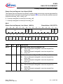
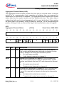
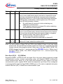
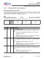
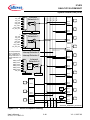
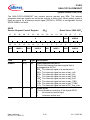
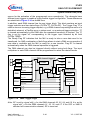
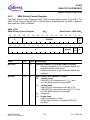
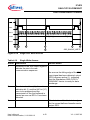
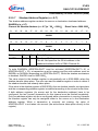
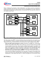
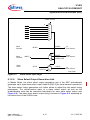
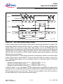
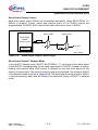
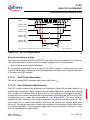
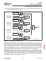
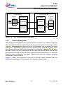
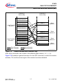
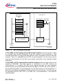
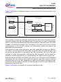
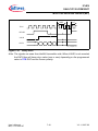
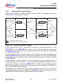
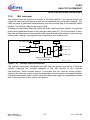
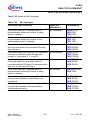
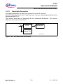
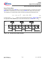
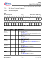
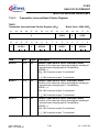
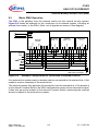
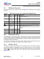
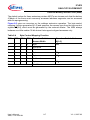
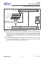
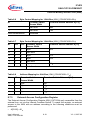
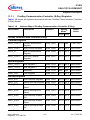
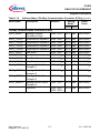
1
User’s Manual, V 2.1, February 2007
SAK-CIC310-OSMX2HT
FlexRay Communication Controller
IFLEX
Microcontrollers
Edition 2007-02
Published by
Infineon Technologies AG
81726 München, Germany
© Infineon Technologies AG 2008.
All Rights Reserved.
Legal Disclaimer
The information given in this document shall in no event be regarded as a guarantee of conditions or
characteristics (“Beschaffenheitsgarantie”). With respect to any examples or hints given herein, any typical values
stated herein and/or any information regarding the application of the device, Infineon Technologies hereby
disclaims any and all warranties and liabilities of any kind, including without limitation warranties of noninfringement of intellectual property rights of any third party.
Information
For further information on technology, delivery terms and conditions and prices please contact your nearest
Infineon Technologies Office (www.infineon.com).
Warnings
Due to technical requirements components may contain dangerous substances. For information on the types in
question please contact your nearest Infineon Technologies Office.
Infineon Technologies Components may only be used in life-support devices or systems with the express written
approval of Infineon Technologies, if a failure of such components can reasonably be expected to cause the failure
of that life-support device or system, or to affect the safety or effectiveness of that device or system. Life support
devices or systems are intended to be implanted in the human body, or to support and/or maintain and sustain
and/or protect human life. If they fail, it is reasonable to assume that the health of the user or other persons may
be endangered.
User’s Manual, V 2.1, February 2007
SAK-CIC310-OSMX2HT
FlexRay Communication Controller
IFLEX
S t e p A 11
Microcontrollers
TriCore™ is a trademark of Infineon Technologies AG
FlexRay™ and the FlexRay logo
are registered trademarks of the FlexRay
Consortium.
We Listen to Your Comments
Any information within this document that you feel is wrong, unclear or missing at all?
Your feedback will help us to continuously improve the quality of this document.
Please send your proposal (including a reference to this document) to:
[email protected]
Template: mc_a5_um_tmplt.fm / 4 / 2004-09-15
IFLEX
SAK-CIC310-OSMX2HT
Table of Contents
Table of Contents
This “Table of Contents” section refers to page numbers in the SAK-CIC310-OSMX2HT
User’s Manual.
1
1.1
1.1.1
1.1.2
1.1.3
1.1.4
1.1.5
1.2
1.3
1.3.1
1.3.2
1.3.3
1.3.4
1.4
1.4.1
1.4.2
1.4.2.1
1.4.2.2
1.4.2.3
Architecture Overview . . . . . . . . . . . . . . . . . . . . . . . . . . . . . . . . . . . . . . 1-1
About this Document . . . . . . . . . . . . . . . . . . . . . . . . . . . . . . . . . . . . . . . . 1-1
Related Documentations . . . . . . . . . . . . . . . . . . . . . . . . . . . . . . . . . . . 1-1
Text Conventions . . . . . . . . . . . . . . . . . . . . . . . . . . . . . . . . . . . . . . . . . 1-1
Reserved, Undefined, and Unimplemented Terminology . . . . . . . . . . 1-3
Register Access Modes . . . . . . . . . . . . . . . . . . . . . . . . . . . . . . . . . . . . 1-5
Abbreviations . . . . . . . . . . . . . . . . . . . . . . . . . . . . . . . . . . . . . . . . . . . . 1-6
Summary of Features . . . . . . . . . . . . . . . . . . . . . . . . . . . . . . . . . . . . . . . 1-9
System Integration Concept . . . . . . . . . . . . . . . . . . . . . . . . . . . . . . . . . 1-11
MLI Host Link (Option One) . . . . . . . . . . . . . . . . . . . . . . . . . . . . . . . . 1-11
SSC Host Link (Option Two) . . . . . . . . . . . . . . . . . . . . . . . . . . . . . . . 1-12
Parallel Host Link (Option Three) . . . . . . . . . . . . . . . . . . . . . . . . . . . 1-14
DMA Controller . . . . . . . . . . . . . . . . . . . . . . . . . . . . . . . . . . . . . . . . . 1-14
General Device Information . . . . . . . . . . . . . . . . . . . . . . . . . . . . . . . . . . 1-17
Block Diagram . . . . . . . . . . . . . . . . . . . . . . . . . . . . . . . . . . . . . . . . . . 1-17
Pin Definition and Functions . . . . . . . . . . . . . . . . . . . . . . . . . . . . . . . 1-19
Package Outline . . . . . . . . . . . . . . . . . . . . . . . . . . . . . . . . . . . . . . 1-19
Pin Description . . . . . . . . . . . . . . . . . . . . . . . . . . . . . . . . . . . . . . . . 1-21
Ordering Information . . . . . . . . . . . . . . . . . . . . . . . . . . . . . . . . . . . 1-33
2
2.1
2.2
2.3
2.4
2.4.1
2.4.2
2.4.2.1
2.4.2.2
2.4.2.3
2.4.2.4
2.4.2.5
2.4.2.6
2.4.2.7
2.4.2.8
2.4.2.9
2.4.2.10
FlexRay Protocol Controller (E-Ray) . . . . . . . . . . . . . . . . . . . . . . . . . . 2-1
Overview . . . . . . . . . . . . . . . . . . . . . . . . . . . . . . . . . . . . . . . . . . . . . . . . . 2-1
Definitions . . . . . . . . . . . . . . . . . . . . . . . . . . . . . . . . . . . . . . . . . . . . . . . . 2-2
Block Diagram . . . . . . . . . . . . . . . . . . . . . . . . . . . . . . . . . . . . . . . . . . . . . 2-2
Programmer’s Model . . . . . . . . . . . . . . . . . . . . . . . . . . . . . . . . . . . . . . . . 2-5
Register Map . . . . . . . . . . . . . . . . . . . . . . . . . . . . . . . . . . . . . . . . . . . . 2-5
E-Ray Kernel Registers . . . . . . . . . . . . . . . . . . . . . . . . . . . . . . . . . . . . 2-6
Customer Registers . . . . . . . . . . . . . . . . . . . . . . . . . . . . . . . . . . . . 2-11
Special Registers . . . . . . . . . . . . . . . . . . . . . . . . . . . . . . . . . . . . . . 2-18
Service Request Registers . . . . . . . . . . . . . . . . . . . . . . . . . . . . . . 2-28
Communication Controller Control Registers . . . . . . . . . . . . . . . . 2-71
Communication Controller Status Registers . . . . . . . . . . . . . . . . . 2-99
Message Buffer Control Registers . . . . . . . . . . . . . . . . . . . . . . . . 2-121
Message Buffer Status Registers . . . . . . . . . . . . . . . . . . . . . . . . 2-128
Identification Registers . . . . . . . . . . . . . . . . . . . . . . . . . . . . . . . . 2-148
Input Buffer . . . . . . . . . . . . . . . . . . . . . . . . . . . . . . . . . . . . . . . . . 2-150
Output Buffer . . . . . . . . . . . . . . . . . . . . . . . . . . . . . . . . . . . . . . . . 2-161
User’s Manual
L-1
V 2.1, 2007-02
IFLEX
SAK-CIC310-OSMX2HT
2.5
2.5.1
2.5.1.1
2.5.1.2
2.5.1.3
2.5.1.4
2.5.1.5
Functional Description . . . . . . . . . . . . . . . . . . . . . . . . . . . . . . . . . . . . .
Communication Cycle . . . . . . . . . . . . . . . . . . . . . . . . . . . . . . . . . . .
Static Segment . . . . . . . . . . . . . . . . . . . . . . . . . . . . . . . . . . . . . .
Dynamic Segment . . . . . . . . . . . . . . . . . . . . . . . . . . . . . . . . . . . .
Symbol Window . . . . . . . . . . . . . . . . . . . . . . . . . . . . . . . . . . . . . .
Network Idle Time (NIT) . . . . . . . . . . . . . . . . . . . . . . . . . . . . . . . .
Configuration of Network Idle Time (NIT) Start and Offset
Correction Start. . . . . . . . . . . . . . . . . . . . . . . . . . . . . . . . . . . . . . .
2.5.2
Communication Modes . . . . . . . . . . . . . . . . . . . . . . . . . . . . . . . . . .
2.5.3
Clock Synchronization . . . . . . . . . . . . . . . . . . . . . . . . . . . . . . . . . . .
2.5.3.1
Global Time . . . . . . . . . . . . . . . . . . . . . . . . . . . . . . . . . . . . . . . . .
2.5.3.2
Local Time . . . . . . . . . . . . . . . . . . . . . . . . . . . . . . . . . . . . . . . . . .
2.5.3.3
Synchronization Process . . . . . . . . . . . . . . . . . . . . . . . . . . . . . . .
2.5.3.4
External Clock Synchronization . . . . . . . . . . . . . . . . . . . . . . . . . .
2.5.4
Error Handling . . . . . . . . . . . . . . . . . . . . . . . . . . . . . . . . . . . . . . . . .
2.5.4.1
Clock Correction Failed Counter . . . . . . . . . . . . . . . . . . . . . . . . .
2.5.4.2
Passive to Active Counter . . . . . . . . . . . . . . . . . . . . . . . . . . . . . .
2.5.4.3
HALT Command . . . . . . . . . . . . . . . . . . . . . . . . . . . . . . . . . . . . .
2.5.4.4
FREEZE Command . . . . . . . . . . . . . . . . . . . . . . . . . . . . . . . . . . .
2.5.5
Communication Controller States . . . . . . . . . . . . . . . . . . . . . . . . . .
2.5.5.1
Communication Controller State Diagram . . . . . . . . . . . . . . . . . .
2.5.5.2
DEFAULT_CONFIG State . . . . . . . . . . . . . . . . . . . . . . . . . . . . . .
2.5.5.3
MONITOR_MODE . . . . . . . . . . . . . . . . . . . . . . . . . . . . . . . . . . . .
2.5.5.4
READY State . . . . . . . . . . . . . . . . . . . . . . . . . . . . . . . . . . . . . . . .
2.5.5.5
WAKEUP State . . . . . . . . . . . . . . . . . . . . . . . . . . . . . . . . . . . . . .
2.5.5.6
STARTUP State . . . . . . . . . . . . . . . . . . . . . . . . . . . . . . . . . . . . . .
2.5.5.7
Startup Timeouts . . . . . . . . . . . . . . . . . . . . . . . . . . . . . . . . . . . . .
2.5.5.8
Path of leading Coldstart Node (initiating coldstart) . . . . . . . . . . .
2.5.5.9
NORMAL_ACTIVE State . . . . . . . . . . . . . . . . . . . . . . . . . . . . . . .
2.5.5.10
NORMAL_PASSIVE State . . . . . . . . . . . . . . . . . . . . . . . . . . . . . .
2.5.5.11
HALT State . . . . . . . . . . . . . . . . . . . . . . . . . . . . . . . . . . . . . . . . .
2.5.6
Network Management . . . . . . . . . . . . . . . . . . . . . . . . . . . . . . . . . . .
2.5.7
Filtering and Masking . . . . . . . . . . . . . . . . . . . . . . . . . . . . . . . . . . . .
2.5.7.1
Frame ID Filtering . . . . . . . . . . . . . . . . . . . . . . . . . . . . . . . . . . . .
2.5.7.2
Channel ID Filtering . . . . . . . . . . . . . . . . . . . . . . . . . . . . . . . . . . .
2.5.7.3
Cycle Counter Filtering . . . . . . . . . . . . . . . . . . . . . . . . . . . . . . . .
2.5.7.4
FIFO Filtering . . . . . . . . . . . . . . . . . . . . . . . . . . . . . . . . . . . . . . . .
2.5.8
Transmit Process . . . . . . . . . . . . . . . . . . . . . . . . . . . . . . . . . . . . . . .
2.5.8.1
Static Segment . . . . . . . . . . . . . . . . . . . . . . . . . . . . . . . . . . . . . .
2.5.8.2
Dynamic Segment . . . . . . . . . . . . . . . . . . . . . . . . . . . . . . . . . . . .
2.5.8.3
Transmit Buffers . . . . . . . . . . . . . . . . . . . . . . . . . . . . . . . . . . . . .
2.5.8.4
Frame Transmission . . . . . . . . . . . . . . . . . . . . . . . . . . . . . . . . . .
2.5.8.5
Null Frame Transmission . . . . . . . . . . . . . . . . . . . . . . . . . . . . . . .
User’s Manual
L-2
2-176
2-176
2-176
2-177
2-177
2-177
2-177
2-179
2-179
2-179
2-179
2-180
2-182
2-182
2-183
2-184
2-184
2-184
2-185
2-185
2-187
2-188
2-188
2-189
2-193
2-196
2-197
2-199
2-199
2-200
2-201
2-201
2-202
2-202
2-203
2-204
2-205
2-205
2-205
2-205
2-207
2-207
V 2.1, 2007-02
IFLEX
SAK-CIC310-OSMX2HT
2.5.9
2.5.9.1
2.5.9.2
2.5.10
2.5.10.1
2.5.10.2
2.5.10.3
2.5.11
2.5.11.1
2.5.11.2
2.5.11.3
2.5.11.4
2.5.12
2.5.12.1
2.5.12.2
2.5.12.3
2.6
2.7
2.7.1
2.7.2
2.8
2.9
Receive Process . . . . . . . . . . . . . . . . . . . . . . . . . . . . . . . . . . . . . . .
Frame Reception . . . . . . . . . . . . . . . . . . . . . . . . . . . . . . . . . . . . .
Null Frame reception . . . . . . . . . . . . . . . . . . . . . . . . . . . . . . . . . .
FIFO Function . . . . . . . . . . . . . . . . . . . . . . . . . . . . . . . . . . . . . . . . .
Description . . . . . . . . . . . . . . . . . . . . . . . . . . . . . . . . . . . . . . . . . .
Configuration of the FIFO . . . . . . . . . . . . . . . . . . . . . . . . . . . . . .
Access to the FIFO . . . . . . . . . . . . . . . . . . . . . . . . . . . . . . . . . . .
Message Handling . . . . . . . . . . . . . . . . . . . . . . . . . . . . . . . . . . . . . .
Host access to Message RAM . . . . . . . . . . . . . . . . . . . . . . . . . . .
Data Transfers between IBF / OBF and Message RAM . . . . . . .
Minimum eray_bclk . . . . . . . . . . . . . . . . . . . . . . . . . . . . . . . . . . .
FlexRay Protocol Controller access to Message RAM . . . . . . . .
Message RAM . . . . . . . . . . . . . . . . . . . . . . . . . . . . . . . . . . . . . . . . .
Header Partition . . . . . . . . . . . . . . . . . . . . . . . . . . . . . . . . . . . . . .
Data Partition . . . . . . . . . . . . . . . . . . . . . . . . . . . . . . . . . . . . . . . .
Parity Check . . . . . . . . . . . . . . . . . . . . . . . . . . . . . . . . . . . . . . . .
Module Service Request . . . . . . . . . . . . . . . . . . . . . . . . . . . . . . . . . . .
Restrictions . . . . . . . . . . . . . . . . . . . . . . . . . . . . . . . . . . . . . . . . . . . . .
Message Buffers with the same Frame ID . . . . . . . . . . . . . . . . . . . .
Data Transfers between IBF / OBF and Message RAM . . . . . . . . .
Known non functional Features of E-Ray Module Revision 1.0.0 . . . .
Revision History . . . . . . . . . . . . . . . . . . . . . . . . . . . . . . . . . . . . . . . . . .
3
3.1
3.2
3.2.1
3.3
3.3.1
3.3.2
3.3.2.1
3.3.3
3.3.3.1
3.3.3.2
3.3.3.3
3.3.4
3.4
3.4.1
3.5
3.5.1
3.5.2
3.5.3
3.5.3.1
System Control Unit (SCU) . . . . . . . . . . . . . . . . . . . . . . . . . . . . . . . . . . 3-1
SCU Registers . . . . . . . . . . . . . . . . . . . . . . . . . . . . . . . . . . . . . . . . . . . . . 3-1
Reset Control Block . . . . . . . . . . . . . . . . . . . . . . . . . . . . . . . . . . . . . . . . . 3-4
Reset Length . . . . . . . . . . . . . . . . . . . . . . . . . . . . . . . . . . . . . . . . . . . . 3-4
Clock System . . . . . . . . . . . . . . . . . . . . . . . . . . . . . . . . . . . . . . . . . . . . . 3-5
Overview . . . . . . . . . . . . . . . . . . . . . . . . . . . . . . . . . . . . . . . . . . . . . . . 3-5
Clock Generation Unit . . . . . . . . . . . . . . . . . . . . . . . . . . . . . . . . . . . . . 3-5
Crystal Oscillator Circuit (COSC) . . . . . . . . . . . . . . . . . . . . . . . . . . . 3-6
Phase-Locked Loop (PLL) Module . . . . . . . . . . . . . . . . . . . . . . . . . . 3-13
PLL Functional Description . . . . . . . . . . . . . . . . . . . . . . . . . . . . . . 3-15
Loss of Oscillator Lock Operation . . . . . . . . . . . . . . . . . . . . . . . . . 3-27
Loss of Oscillator Lock Recovery . . . . . . . . . . . . . . . . . . . . . . . . . 3-28
Clock Multiplex Unit . . . . . . . . . . . . . . . . . . . . . . . . . . . . . . . . . . . . . . 3-28
Power Supply System . . . . . . . . . . . . . . . . . . . . . . . . . . . . . . . . . . . . . . 3-30
Miscellaneous SCU Registers . . . . . . . . . . . . . . . . . . . . . . . . . . . . . . 3-31
Interrupt Control . . . . . . . . . . . . . . . . . . . . . . . . . . . . . . . . . . . . . . . . . . . 3-33
Internal Interconnection Signals . . . . . . . . . . . . . . . . . . . . . . . . . . . . 3-34
External Trigger Inputs . . . . . . . . . . . . . . . . . . . . . . . . . . . . . . . . . . . 3-34
Interrupt Output Structure . . . . . . . . . . . . . . . . . . . . . . . . . . . . . . . . . 3-38
Communication Relations . . . . . . . . . . . . . . . . . . . . . . . . . . . . . . . 3-38
User’s Manual
L-3
2-207
2-208
2-208
2-209
2-209
2-210
2-211
2-211
2-211
2-217
2-223
2-227
2-228
2-230
2-233
2-234
2-237
2-240
2-240
2-240
2-241
2-251
V 2.1, 2007-02
IFLEX
SAK-CIC310-OSMX2HT
3.5.3.2
3.5.4
3.6
3.6.1
3.6.2
3.6.3
3.6.4
3.6.5
3.6.6
Service Request Routing . . . . . . . . . . . . . . . . . . . . . . . . . . . . . . . .
DMA Channel Trigger . . . . . . . . . . . . . . . . . . . . . . . . . . . . . . . . . . . .
Mode Selection . . . . . . . . . . . . . . . . . . . . . . . . . . . . . . . . . . . . . . . . . . .
MODE 0 and Mode 1 Pin . . . . . . . . . . . . . . . . . . . . . . . . . . . . . . . . . .
JTAGEN Pin . . . . . . . . . . . . . . . . . . . . . . . . . . . . . . . . . . . . . . . . . . .
XMU Global Control Register . . . . . . . . . . . . . . . . . . . . . . . . . . . . . .
DMA Reprogramming . . . . . . . . . . . . . . . . . . . . . . . . . . . . . . . . . . . .
Gather Scattered Bits . . . . . . . . . . . . . . . . . . . . . . . . . . . . . . . . . . . .
Address Map . . . . . . . . . . . . . . . . . . . . . . . . . . . . . . . . . . . . . . . . . . .
4
4.1
4.1.1
4.1.2
4.1.3
4.2
4.2.1
4.2.2
4.2.3
4.3
4.4
4.4.1
4.4.2
4.4.3
4.4.4
4.4.4.1
4.4.4.2
4.5
4.5.1
4.5.2
4.5.3
4.5.4
4.5.5
Host Communication Channels . . . . . . . . . . . . . . . . . . . . . . . . . . . . . . 4-1
Host Write Request . . . . . . . . . . . . . . . . . . . . . . . . . . . . . . . . . . . . . . . . . 4-1
MLI Write Operation . . . . . . . . . . . . . . . . . . . . . . . . . . . . . . . . . . . . . . . 4-1
SSC Write Operation . . . . . . . . . . . . . . . . . . . . . . . . . . . . . . . . . . . . . . 4-2
XMU Write Operation . . . . . . . . . . . . . . . . . . . . . . . . . . . . . . . . . . . . . . 4-2
Host Read Request . . . . . . . . . . . . . . . . . . . . . . . . . . . . . . . . . . . . . . . . . 4-2
MLI Read Operation . . . . . . . . . . . . . . . . . . . . . . . . . . . . . . . . . . . . . . 4-2
SSC Read Operation . . . . . . . . . . . . . . . . . . . . . . . . . . . . . . . . . . . . . . 4-3
XMU Read Operation . . . . . . . . . . . . . . . . . . . . . . . . . . . . . . . . . . . . . 4-3
SSC Move Engine . . . . . . . . . . . . . . . . . . . . . . . . . . . . . . . . . . . . . . . . . . 4-4
Communication Principles MLI . . . . . . . . . . . . . . . . . . . . . . . . . . . . . . . . 4-8
Prerequisites for Communication . . . . . . . . . . . . . . . . . . . . . . . . . . . . . 4-9
Enable MLI Interfaces . . . . . . . . . . . . . . . . . . . . . . . . . . . . . . . . . . . . . 4-9
Single steps of Communication via MLI bridge . . . . . . . . . . . . . . . . . 4-10
DMA Support for MLI (Single Message Buffer Read Support) . . . . . 4-10
Single Message Buffer Read Support . . . . . . . . . . . . . . . . . . . . . . 4-10
Periodically Copy Message Buffer Contents to Host Memory . . . . 4-21
Communication Principles SSC . . . . . . . . . . . . . . . . . . . . . . . . . . . . . . . 4-39
Single Read Access via SSC . . . . . . . . . . . . . . . . . . . . . . . . . . . . . . . 4-45
Consecutive Read Accesses via SSC . . . . . . . . . . . . . . . . . . . . . . . . 4-47
Single Write Access via SSC . . . . . . . . . . . . . . . . . . . . . . . . . . . . . . . 4-51
Consecutive Write Access via SSC . . . . . . . . . . . . . . . . . . . . . . . . . . 4-53
Error Handling . . . . . . . . . . . . . . . . . . . . . . . . . . . . . . . . . . . . . . . . . . 4-57
5
5.1
5.1.1
5.1.2
5.1.3
5.1.4
5.1.5
5.1.5.1
5.1.5.2
5.1.5.3
Direct Memory Access Controller (DMA) . . . . . . . . . . . . . . . . . . . . . .
DMA Controller Description . . . . . . . . . . . . . . . . . . . . . . . . . . . . . . . . . . .
Features . . . . . . . . . . . . . . . . . . . . . . . . . . . . . . . . . . . . . . . . . . . . . . . .
Definition of Terms . . . . . . . . . . . . . . . . . . . . . . . . . . . . . . . . . . . . . . . .
DMA Principle . . . . . . . . . . . . . . . . . . . . . . . . . . . . . . . . . . . . . . . . . . .
DMA Block Diagram . . . . . . . . . . . . . . . . . . . . . . . . . . . . . . . . . . . . . .
DMA Operation Functionality . . . . . . . . . . . . . . . . . . . . . . . . . . . . . . . .
Shadow Registers . . . . . . . . . . . . . . . . . . . . . . . . . . . . . . . . . . . . . .
DMA Channel Request Control . . . . . . . . . . . . . . . . . . . . . . . . . . . .
DMA Channel Operation Mode . . . . . . . . . . . . . . . . . . . . . . . . . . . .
User’s Manual
L-4
3-39
3-43
3-46
3-46
3-46
3-47
3-49
3-51
3-55
5-1
5-1
5-1
5-2
5-3
5-4
5-4
5-5
5-8
5-8
V 2.1, 2007-02
IFLEX
SAK-CIC310-OSMX2HT
5.1.5.4
Move Count . . . . . . . . . . . . . . . . . . . . . . . . . . . . . . . . . . . . . . . . . .
5.1.5.5
Request Lost . . . . . . . . . . . . . . . . . . . . . . . . . . . . . . . . . . . . . . . . .
5.1.5.6
Circular Buffer . . . . . . . . . . . . . . . . . . . . . . . . . . . . . . . . . . . . . . . .
5.1.5.7
Interrupt Signal Generation . . . . . . . . . . . . . . . . . . . . . . . . . . . . . .
5.1.5.8
Pattern Detection . . . . . . . . . . . . . . . . . . . . . . . . . . . . . . . . . . . . . .
5.1.5.9
Error Conditions . . . . . . . . . . . . . . . . . . . . . . . . . . . . . . . . . . . . . . .
5.1.5.10
Channel Reset Operation . . . . . . . . . . . . . . . . . . . . . . . . . . . . . . .
5.1.5.11
Programmable Address Modification . . . . . . . . . . . . . . . . . . . . . . .
5.1.6
Transaction Control Engine . . . . . . . . . . . . . . . . . . . . . . . . . . . . . . . .
5.1.7
Request Assignment Unit . . . . . . . . . . . . . . . . . . . . . . . . . . . . . . . . .
5.1.8
General Interrupt Structure . . . . . . . . . . . . . . . . . . . . . . . . . . . . . . . .
5.2
DMA Module Kernel Registers . . . . . . . . . . . . . . . . . . . . . . . . . . . . . . .
5.2.1
Overview . . . . . . . . . . . . . . . . . . . . . . . . . . . . . . . . . . . . . . . . . . . . . .
5.2.2
Identification Register . . . . . . . . . . . . . . . . . . . . . . . . . . . . . . . . . . . .
5.2.2.1
DMA Module Identification Register . . . . . . . . . . . . . . . . . . . . . . .
5.2.2.2
Global Interrupt Set Register . . . . . . . . . . . . . . . . . . . . . . . . . . . . .
5.2.3
General Control and Status Registers . . . . . . . . . . . . . . . . . . . . . . . .
5.2.3.1
Channel Reset Request Register . . . . . . . . . . . . . . . . . . . . . . . . .
5.2.3.2
Transaction Request State Register . . . . . . . . . . . . . . . . . . . . . . .
5.2.3.3
Software Transaction Request Register . . . . . . . . . . . . . . . . . . . .
5.2.3.4
Hardware Transaction Request Register . . . . . . . . . . . . . . . . . . . .
5.2.3.5
Enable Error Register . . . . . . . . . . . . . . . . . . . . . . . . . . . . . . . . . .
5.2.3.6
Error Status Register . . . . . . . . . . . . . . . . . . . . . . . . . . . . . . . . . . .
5.2.3.7
Clear Error Register . . . . . . . . . . . . . . . . . . . . . . . . . . . . . . . . . . . .
5.2.3.8
Interrupt Status Register . . . . . . . . . . . . . . . . . . . . . . . . . . . . . . . .
5.2.3.9
Wrap Status Register . . . . . . . . . . . . . . . . . . . . . . . . . . . . . . . . . . .
5.2.3.10
Interrupt Clear Register . . . . . . . . . . . . . . . . . . . . . . . . . . . . . . . . .
5.2.4
Move Engine Registers . . . . . . . . . . . . . . . . . . . . . . . . . . . . . . . . . . .
5.2.4.1
Move Engine Status Register . . . . . . . . . . . . . . . . . . . . . . . . . . . .
5.2.4.2
Move Engine 0 Read Register . . . . . . . . . . . . . . . . . . . . . . . . . . . .
5.2.4.3
Move Engine 0 Pattern Register . . . . . . . . . . . . . . . . . . . . . . . . . .
5.2.5
Channel Control, Status and Address Registers . . . . . . . . . . . . . . . .
5.2.5.1
Channel 0n Control Register (n = 0-7) . . . . . . . . . . . . . . . . . . . . . .
5.2.5.2
Channel 0n Status Register (n = 0-7) . . . . . . . . . . . . . . . . . . . . . .
5.2.5.3
Channel Interrupt Control Register (n = 0-7) . . . . . . . . . . . . . . . . .
5.2.5.4
Address Control Register (n = 0-7) . . . . . . . . . . . . . . . . . . . . . . . .
5.2.5.5
Source Address Register (n = 0-7) . . . . . . . . . . . . . . . . . . . . . . . .
5.2.5.6
Destination Address Register (n = 0-7) . . . . . . . . . . . . . . . . . . . . .
5.2.5.7
Shadow Address Register (n = 0-7) . . . . . . . . . . . . . . . . . . . . . . .
5.3
DMA Module Implementation . . . . . . . . . . . . . . . . . . . . . . . . . . . . . . . .
5.3.1
DMA Request Assignment Matrix . . . . . . . . . . . . . . . . . . . . . . . . . . .
5.3.2
Address Map . . . . . . . . . . . . . . . . . . . . . . . . . . . . . . . . . . . . . . . . . . .
User’s Manual
L-5
5-12
5-12
5-13
5-14
5-14
5-16
5-16
5-17
5-19
5-20
5-21
5-22
5-22
5-25
5-25
5-26
5-27
5-27
5-28
5-29
5-30
5-31
5-33
5-35
5-37
5-38
5-39
5-40
5-40
5-42
5-43
5-45
5-45
5-49
5-50
5-52
5-55
5-56
5-57
5-58
5-58
5-61
V 2.1, 2007-02
IFLEX
SAK-CIC310-OSMX2HT
6
6.1
6.1.1
6.1.2
6.1.2.1
6.1.2.2
6.1.2.3
6.1.2.4
6.1.2.5
6.1.2.6
6.1.2.7
6.1.2.8
6.1.2.9
6.1.2.10
6.2
6.3
6.3.1
6.3.1.1
6.3.1.2
6.3.1.3
6.3.1.4
6.3.1.5
6.3.1.6
6.3.2
6.3.3
6.3.4
Synchronous Serial Interface (SSC) . . . . . . . . . . . . . . . . . . . . . . . . . . 6-1
SSC Kernel Description . . . . . . . . . . . . . . . . . . . . . . . . . . . . . . . . . . . . . . 6-1
Overview . . . . . . . . . . . . . . . . . . . . . . . . . . . . . . . . . . . . . . . . . . . . . . . 6-1
General Operation . . . . . . . . . . . . . . . . . . . . . . . . . . . . . . . . . . . . . . . . 6-2
Operating Mode Selection . . . . . . . . . . . . . . . . . . . . . . . . . . . . . . . . 6-3
Full-Duplex Operation . . . . . . . . . . . . . . . . . . . . . . . . . . . . . . . . . . . 6-5
Half-Duplex Operation . . . . . . . . . . . . . . . . . . . . . . . . . . . . . . . . . . . 6-7
Continuous Transfers . . . . . . . . . . . . . . . . . . . . . . . . . . . . . . . . . . . 6-9
Port Control . . . . . . . . . . . . . . . . . . . . . . . . . . . . . . . . . . . . . . . . . . . 6-9
Baud Rate Generation . . . . . . . . . . . . . . . . . . . . . . . . . . . . . . . . . . 6-10
Slave Select Input Operation . . . . . . . . . . . . . . . . . . . . . . . . . . . . . 6-12
Slave Select Output Generation Unit . . . . . . . . . . . . . . . . . . . . . . . 6-13
Shift Clock Generation . . . . . . . . . . . . . . . . . . . . . . . . . . . . . . . . . . 6-16
Error Detection Mechanisms . . . . . . . . . . . . . . . . . . . . . . . . . . . . . 6-16
SSC Kernel Registers . . . . . . . . . . . . . . . . . . . . . . . . . . . . . . . . . . . . . . 6-19
SSC Module Implementation . . . . . . . . . . . . . . . . . . . . . . . . . . . . . . . . . 6-35
Interfaces of the SSC Module . . . . . . . . . . . . . . . . . . . . . . . . . . . . . . 6-35
Port Connections of SSC . . . . . . . . . . . . . . . . . . . . . . . . . . . . . . . . 6-35
Interface signals of SSC . . . . . . . . . . . . . . . . . . . . . . . . . . . . . . . . 6-35
RDY signal . . . . . . . . . . . . . . . . . . . . . . . . . . . . . . . . . . . . . . . . . . . 6-35
DIR Signal . . . . . . . . . . . . . . . . . . . . . . . . . . . . . . . . . . . . . . . . . . . 6-36
Connecting 2 or more slaves to 1 host . . . . . . . . . . . . . . . . . . . . . 6-36
Half-Duplex Control . . . . . . . . . . . . . . . . . . . . . . . . . . . . . . . . . . . . 6-37
Error Handling . . . . . . . . . . . . . . . . . . . . . . . . . . . . . . . . . . . . . . . . . . 6-38
Reset Initialization . . . . . . . . . . . . . . . . . . . . . . . . . . . . . . . . . . . . . . . 6-40
Address Map . . . . . . . . . . . . . . . . . . . . . . . . . . . . . . . . . . . . . . . . . . . 6-41
7
7.1
7.2
7.2.1
7.2.1.1
7.2.1.2
7.2.2
7.2.3
7.2.4
7.2.5
7.2.6
7.2.6.1
7.2.6.2
7.2.6.3
7.2.6.4
7.2.6.5
Micro Link Serial Bus Interface (MLI) . . . . . . . . . . . . . . . . . . . . . . . . . . 7-1
MLI Applications . . . . . . . . . . . . . . . . . . . . . . . . . . . . . . . . . . . . . . . . . . . 7-1
MLI Kernel Description . . . . . . . . . . . . . . . . . . . . . . . . . . . . . . . . . . . . . . 7-3
Overview . . . . . . . . . . . . . . . . . . . . . . . . . . . . . . . . . . . . . . . . . . . . . . . 7-3
Naming Conventions . . . . . . . . . . . . . . . . . . . . . . . . . . . . . . . . . . . . 7-4
MLI Communication Principles . . . . . . . . . . . . . . . . . . . . . . . . . . . . 7-5
General Description . . . . . . . . . . . . . . . . . . . . . . . . . . . . . . . . . . . . . . . 7-6
Handshake Description . . . . . . . . . . . . . . . . . . . . . . . . . . . . . . . . . . . 7-13
Startup Procedure . . . . . . . . . . . . . . . . . . . . . . . . . . . . . . . . . . . . . . . 7-15
MLI Kernel and MLI Interface Logical Connection . . . . . . . . . . . . . . . 7-16
MLI Transmitter . . . . . . . . . . . . . . . . . . . . . . . . . . . . . . . . . . . . . . . . . 7-17
MLI Transmitter Reset . . . . . . . . . . . . . . . . . . . . . . . . . . . . . . . . . . 7-17
MLI Transmitter Operation Modes . . . . . . . . . . . . . . . . . . . . . . . . . 7-17
Internal Architecture And Interface Signals . . . . . . . . . . . . . . . . . . 7-19
Transmission Format . . . . . . . . . . . . . . . . . . . . . . . . . . . . . . . . . . . 7-20
Transmission Modes . . . . . . . . . . . . . . . . . . . . . . . . . . . . . . . . . . . 7-21
User’s Manual
L-6
V 2.1, 2007-02
IFLEX
SAK-CIC310-OSMX2HT
7.2.6.6
Transfer Mode Selection . . . . . . . . . . . . . . . . . . . . . . . . . . . . . . . .
7.2.6.7
Parity Generation . . . . . . . . . . . . . . . . . . . . . . . . . . . . . . . . . . . . . .
7.2.6.8
Error Detection and Handling . . . . . . . . . . . . . . . . . . . . . . . . . . . .
7.2.6.9
MLI Transmitter Input/Output Control . . . . . . . . . . . . . . . . . . . . . .
7.2.7
MLI Receiver . . . . . . . . . . . . . . . . . . . . . . . . . . . . . . . . . . . . . . . . . . .
7.2.7.1
MLI Receiver Reset . . . . . . . . . . . . . . . . . . . . . . . . . . . . . . . . . . . .
7.2.7.2
MLI Receiver Operation Modes . . . . . . . . . . . . . . . . . . . . . . . . . . .
7.2.7.3
Internal Architecture And Interface Signals . . . . . . . . . . . . . . . . . .
7.2.7.4
MLI Receiver Operation . . . . . . . . . . . . . . . . . . . . . . . . . . . . . . . . .
7.2.7.5
Error Handling . . . . . . . . . . . . . . . . . . . . . . . . . . . . . . . . . . . . . . . .
7.2.7.6
MLI Receiver Input/Output Control . . . . . . . . . . . . . . . . . . . . . . . .
7.2.8
Reading Process Summary . . . . . . . . . . . . . . . . . . . . . . . . . . . . . . . .
7.2.9
MLI Interrupts . . . . . . . . . . . . . . . . . . . . . . . . . . . . . . . . . . . . . . . . . . .
7.2.10
Clock Domains and Handshake Timing . . . . . . . . . . . . . . . . . . . . . . .
7.2.11
Data Flow Description . . . . . . . . . . . . . . . . . . . . . . . . . . . . . . . . . . . .
7.2.11.1
Copy Base Address . . . . . . . . . . . . . . . . . . . . . . . . . . . . . . . . . . . .
7.2.11.2
Command Frame . . . . . . . . . . . . . . . . . . . . . . . . . . . . . . . . . . . . . .
7.2.11.3
Write Frame . . . . . . . . . . . . . . . . . . . . . . . . . . . . . . . . . . . . . . . . . .
7.2.11.4
Read Frame . . . . . . . . . . . . . . . . . . . . . . . . . . . . . . . . . . . . . . . . . .
7.2.11.5
Access to Remote Window . . . . . . . . . . . . . . . . . . . . . . . . . . . . . .
7.2.12
Baud Rate Generation . . . . . . . . . . . . . . . . . . . . . . . . . . . . . . . . . . . .
7.2.12.1
Fractional Divider . . . . . . . . . . . . . . . . . . . . . . . . . . . . . . . . . . . . . .
7.3
MLI Kernel Registers . . . . . . . . . . . . . . . . . . . . . . . . . . . . . . . . . . . . . . .
7.3.1
Module Identification Register . . . . . . . . . . . . . . . . . . . . . . . . . . . . . .
7.3.2
MLI Transmitter Registers . . . . . . . . . . . . . . . . . . . . . . . . . . . . . . . . .
7.3.2.1
Transmitter Control Register . . . . . . . . . . . . . . . . . . . . . . . . . . . . .
7.3.2.2
Transmitter Status Register . . . . . . . . . . . . . . . . . . . . . . . . . . . . . .
7.3.2.3
Transmitter Pipe Status Registers . . . . . . . . . . . . . . . . . . . . . . . . .
7.3.2.4
Transmitter Command Register . . . . . . . . . . . . . . . . . . . . . . . . . . .
7.3.2.5
Transmitter Registers Status Register . . . . . . . . . . . . . . . . . . . . . .
7.3.2.6
Transmitter Pipe Address Offset Registers . . . . . . . . . . . . . . . . . .
7.3.2.7
Transmitter Pipe Data Registers . . . . . . . . . . . . . . . . . . . . . . . . . .
7.3.2.8
Transmitter Data Read Answer Register . . . . . . . . . . . . . . . . . . . .
7.3.2.9
Transmitter Pipe Base Address Registers . . . . . . . . . . . . . . . . . . .
7.3.2.10
Transmitter Copy Base Address Register . . . . . . . . . . . . . . . . . . .
7.3.3
MLI Receiver Registers . . . . . . . . . . . . . . . . . . . . . . . . . . . . . . . . . . .
7.3.3.1
Receiver Control Register . . . . . . . . . . . . . . . . . . . . . . . . . . . . . . .
7.3.3.2
Receiver Pipe Base Address Registers . . . . . . . . . . . . . . . . . . . . .
7.3.3.3
Receiver Pipe Status Registers . . . . . . . . . . . . . . . . . . . . . . . . . . .
7.3.3.4
Receiver Address Register . . . . . . . . . . . . . . . . . . . . . . . . . . . . . .
7.3.4
Receiver Data Register . . . . . . . . . . . . . . . . . . . . . . . . . . . . . . . . . . .
7.3.5
MLI Kernel Common Registers . . . . . . . . . . . . . . . . . . . . . . . . . . . . .
7.3.5.1
Set Clear Register . . . . . . . . . . . . . . . . . . . . . . . . . . . . . . . . . . . . .
User’s Manual
L-7
7-28
7-31
7-31
7-33
7-34
7-34
7-34
7-36
7-36
7-42
7-44
7-46
7-47
7-50
7-54
7-54
7-55
7-56
7-57
7-59
7-60
7-61
7-64
7-67
7-68
7-68
7-71
7-73
7-75
7-77
7-79
7-80
7-81
7-82
7-83
7-84
7-84
7-87
7-88
7-89
7-90
7-91
7-91
V 2.1, 2007-02
IFLEX
SAK-CIC310-OSMX2HT
7.3.6
7.3.6.1
7.3.6.2
7.3.6.3
7.3.6.4
7.3.6.5
7.3.6.6
7.3.6.7
7.3.6.8
7.3.6.9
7.4
7.4.1
7.4.1.1
7.4.1.2
7.4.2
MLI Interrupt Registers . . . . . . . . . . . . . . . . . . . . . . . . . . . . . . . . . . . 7-93
Transmitter Interrupt Enable Register . . . . . . . . . . . . . . . . . . . . . . 7-93
Transmitter Interrupt Status Register . . . . . . . . . . . . . . . . . . . . . . . 7-95
Transmitter Interrupt Node Pointer Register . . . . . . . . . . . . . . . . . 7-96
Receiver Interrupt Enable Register . . . . . . . . . . . . . . . . . . . . . . . . 7-98
Receiver Interrupt Status Register . . . . . . . . . . . . . . . . . . . . . . . . 7-100
Receiver Interrupt Node Pointer Register . . . . . . . . . . . . . . . . . . 7-101
Global Interrupt Set Register . . . . . . . . . . . . . . . . . . . . . . . . . . . . 7-103
Output Input Control Register . . . . . . . . . . . . . . . . . . . . . . . . . . . 7-104
Fractional Divider Registers . . . . . . . . . . . . . . . . . . . . . . . . . . . . . 7-109
MLI Module Implementation . . . . . . . . . . . . . . . . . . . . . . . . . . . . . . . . 7-111
Interfaces of the MLI Module . . . . . . . . . . . . . . . . . . . . . . . . . . . . . . 7-111
Port Connections of MLI . . . . . . . . . . . . . . . . . . . . . . . . . . . . . . . 7-111
Interface signals of MLI . . . . . . . . . . . . . . . . . . . . . . . . . . . . . . . . 7-111
Address Map . . . . . . . . . . . . . . . . . . . . . . . . . . . . . . . . . . . . . . . . . . 7-112
8
8.1
8.2
8.3
8.4
8.4.1
8.4.2
8.4.2.1
8.4.3
8.4.4
8.4.5
8.4.6
8.5
8.5.1
8.5.2
8.5.3
8.5.4
8.5.5
8.5.6
8.6
8.6.1
8.6.2
8.7
8.7.1
8.7.2
8.7.3
8.8
External Memory Interface Unit (XMU) . . . . . . . . . . . . . . . . . . . . . . . . 8-1
Overview . . . . . . . . . . . . . . . . . . . . . . . . . . . . . . . . . . . . . . . . . . . . . . . . . 8-1
XMU Features . . . . . . . . . . . . . . . . . . . . . . . . . . . . . . . . . . . . . . . . . . . . . 8-1
Basic XMU Operation . . . . . . . . . . . . . . . . . . . . . . . . . . . . . . . . . . . . . . . 8-2
XMU Signal Description . . . . . . . . . . . . . . . . . . . . . . . . . . . . . . . . . . . . . . 8-3
Address Bus, A[12:0] . . . . . . . . . . . . . . . . . . . . . . . . . . . . . . . . . . . . . . 8-3
Data Bus, D[16:0] . . . . . . . . . . . . . . . . . . . . . . . . . . . . . . . . . . . . . . . . 8-3
Data Bus Direction Control . . . . . . . . . . . . . . . . . . . . . . . . . . . . . . . 8-4
Read and Write Strobes, RD and WR . . . . . . . . . . . . . . . . . . . . . . . . . 8-4
Byte Control Signals, BCx . . . . . . . . . . . . . . . . . . . . . . . . . . . . . . . . . . 8-4
Variable Wait State Control, WAIT . . . . . . . . . . . . . . . . . . . . . . . . . . . 8-4
XMU Chip Select, CSFPI . . . . . . . . . . . . . . . . . . . . . . . . . . . . . . . . . . . 8-5
Detailed External to Internal XMU Operation . . . . . . . . . . . . . . . . . . . . . . 8-5
XMU Signal Direction . . . . . . . . . . . . . . . . . . . . . . . . . . . . . . . . . . . . . . 8-5
Address Translation . . . . . . . . . . . . . . . . . . . . . . . . . . . . . . . . . . . . . . . 8-6
External to Internal Access Controls . . . . . . . . . . . . . . . . . . . . . . . . . . 8-9
Basic Access Timing . . . . . . . . . . . . . . . . . . . . . . . . . . . . . . . . . . . . . . 8-9
External Requests to the XMU . . . . . . . . . . . . . . . . . . . . . . . . . . . . . 8-12
Bidirectional Data Lines . . . . . . . . . . . . . . . . . . . . . . . . . . . . . . . . . . . 8-12
XMU Registers . . . . . . . . . . . . . . . . . . . . . . . . . . . . . . . . . . . . . . . . . . . . 8-13
Global Control Register . . . . . . . . . . . . . . . . . . . . . . . . . . . . . . . . . . . 8-13
Byte Control Select . . . . . . . . . . . . . . . . . . . . . . . . . . . . . . . . . . . . . . 8-14
XMU Module Implementation . . . . . . . . . . . . . . . . . . . . . . . . . . . . . . . . 8-16
Interfaces of the XMU Module . . . . . . . . . . . . . . . . . . . . . . . . . . . . . . 8-16
External Address Extension . . . . . . . . . . . . . . . . . . . . . . . . . . . . . . . . 8-16
External Access Configuration Register . . . . . . . . . . . . . . . . . . . . . . 8-19
Supported Address Range . . . . . . . . . . . . . . . . . . . . . . . . . . . . . . . . . . 8-21
User’s Manual
L-8
V 2.1, 2007-02
IFLEX
SAK-CIC310-OSMX2HT
9
9.1
9.1.1
9.1.1.1
9.1.2
9.1.2.1
9.1.2.2
9.1.2.3
9.1.2.4
9.1.3
9.1.3.1
9.1.3.2
9.1.3.3
9.1.3.4
9.1.3.5
9.2
9.2.1
9.2.2
9.2.2.1
9.2.2.2
9.2.2.3
9.2.3
9.2.3.1
9.2.3.2
9.2.3.3
9.2.4
9.2.4.1
9.2.4.2
9.2.4.3
9.3
Parallel Ports (PORTS) . . . . . . . . . . . . . . . . . . . . . . . . . . . . . . . . . . . . . 9-1
General Description . . . . . . . . . . . . . . . . . . . . . . . . . . . . . . . . . . . . . . . . . 9-1
Input Stage Control . . . . . . . . . . . . . . . . . . . . . . . . . . . . . . . . . . . . . . . 9-1
Reset Behavior . . . . . . . . . . . . . . . . . . . . . . . . . . . . . . . . . . . . . . . . 9-2
Output Driver Control . . . . . . . . . . . . . . . . . . . . . . . . . . . . . . . . . . . . . . 9-2
Reset Behavior . . . . . . . . . . . . . . . . . . . . . . . . . . . . . . . . . . . . . . . . 9-2
Power-fail Behavior . . . . . . . . . . . . . . . . . . . . . . . . . . . . . . . . . . . . . 9-2
Pad Driver Control . . . . . . . . . . . . . . . . . . . . . . . . . . . . . . . . . . . . . . 9-2
Port Control Coding . . . . . . . . . . . . . . . . . . . . . . . . . . . . . . . . . . . . . 9-4
Port Register Description . . . . . . . . . . . . . . . . . . . . . . . . . . . . . . . . . . . 9-5
Port Output Register . . . . . . . . . . . . . . . . . . . . . . . . . . . . . . . . . . . . 9-5
Port Output Modification Register . . . . . . . . . . . . . . . . . . . . . . . . . . 9-6
Port Input Register . . . . . . . . . . . . . . . . . . . . . . . . . . . . . . . . . . . . . . 9-7
Port Input/Output Control Registers . . . . . . . . . . . . . . . . . . . . . . . . . 9-8
Pad Driver Mode Register . . . . . . . . . . . . . . . . . . . . . . . . . . . . . . . 9-12
Pin Description . . . . . . . . . . . . . . . . . . . . . . . . . . . . . . . . . . . . . . . . . . . . 9-13
Device Pinning Overview . . . . . . . . . . . . . . . . . . . . . . . . . . . . . . . . . . 9-13
Port 0 Registers . . . . . . . . . . . . . . . . . . . . . . . . . . . . . . . . . . . . . . . . . 9-13
Overview . . . . . . . . . . . . . . . . . . . . . . . . . . . . . . . . . . . . . . . . . . . . 9-13
Port 0 Register Implementations . . . . . . . . . . . . . . . . . . . . . . . . . . 9-15
Port 0 Functions . . . . . . . . . . . . . . . . . . . . . . . . . . . . . . . . . . . . . . . 9-26
Port 1 Registers . . . . . . . . . . . . . . . . . . . . . . . . . . . . . . . . . . . . . . . . . 9-29
Overview . . . . . . . . . . . . . . . . . . . . . . . . . . . . . . . . . . . . . . . . . . . . 9-29
Port 1 Register Implementations . . . . . . . . . . . . . . . . . . . . . . . . . . 9-30
Port 1 Functions . . . . . . . . . . . . . . . . . . . . . . . . . . . . . . . . . . . . . . . 9-41
Port 2 Registers . . . . . . . . . . . . . . . . . . . . . . . . . . . . . . . . . . . . . . . . . 9-45
Overview . . . . . . . . . . . . . . . . . . . . . . . . . . . . . . . . . . . . . . . . . . . . 9-45
Port 2 Register Implementations . . . . . . . . . . . . . . . . . . . . . . . . . . 9-46
Port 2 Functions . . . . . . . . . . . . . . . . . . . . . . . . . . . . . . . . . . . . . . . 9-53
Address Map . . . . . . . . . . . . . . . . . . . . . . . . . . . . . . . . . . . . . . . . . . . . . 9-56
10
Initialization of the SAK-CIC310-OSMX2HT Chip . . . . . . . . . . . . . . .
10.1
Initialization for MLI Communication . . . . . . . . . . . . . . . . . . . . . . . . . . .
10.1.1
The Initialization Values of Port 0 . . . . . . . . . . . . . . . . . . . . . . . . . . .
10.1.2
The Initialization Values of Port 1 . . . . . . . . . . . . . . . . . . . . . . . . . . .
10.1.3
The Initialization Values of Port 2 . . . . . . . . . . . . . . . . . . . . . . . . . . .
10.1.4
Initialization Values of MLI . . . . . . . . . . . . . . . . . . . . . . . . . . . . . . . . .
10.1.5
The Initialization Values of the Service Request Control . . . . . . . . . .
10.2
Initialization for XMU Communication . . . . . . . . . . . . . . . . . . . . . . . . . .
10.2.1
The Initialization Values of Port 0 . . . . . . . . . . . . . . . . . . . . . . . . . . .
10.2.2
The Initialization Values of Port 1 . . . . . . . . . . . . . . . . . . . . . . . . . . .
10.2.2.1
XMU with 16-bit Data Width . . . . . . . . . . . . . . . . . . . . . . . . . . . .
10.2.3
The Initialization Values of Port 2 . . . . . . . . . . . . . . . . . . . . . . . . . . .
User’s Manual
L-9
10-1
10-2
10-2
10-2
10-3
10-3
10-3
10-4
10-4
10-4
10-5
10-5
V 2.1, 2007-02
IFLEX
SAK-CIC310-OSMX2HT
10.2.4
Initialization Values of the XMU . . . . . . . . . . . . . . . . . . . . . . . . . . . . . 10-6
10.2.5
The Initialization Values of the Service Request Control . . . . . . . . . . 10-6
10.3
Initialization for SSC/SPI Communication . . . . . . . . . . . . . . . . . . . . . . . 10-6
10.3.1
The Initialization Values of Port 0 . . . . . . . . . . . . . . . . . . . . . . . . . . . 10-7
10.3.2
The Initialization Values of Port 1 . . . . . . . . . . . . . . . . . . . . . . . . . . . 10-7
10.3.2.1
SSC Full-Duplex Mode . . . . . . . . . . . . . . . . . . . . . . . . . . . . . . . . . 10-7
10.3.2.2
SSC Half-Duplex Mode . . . . . . . . . . . . . . . . . . . . . . . . . . . . . . . . . 10-8
10.3.3
The Initialization Values of Port 2 . . . . . . . . . . . . . . . . . . . . . . . . . . . 10-8
10.3.4
The Initialization Values of the SSC . . . . . . . . . . . . . . . . . . . . . . . . . 10-9
10.3.5
The Initialization Values of the Service Request Control . . . . . . . . . 10-10
11
11.1
11.1.1
11.1.2
11.1.3
11.1.4
11.1.5
11.1.6
11.1.7
11.1.8
Register Description . . . . . . . . . . . . . . . . . . . . . . . . . . . . . . . . . . . . . . 11-1
Overview . . . . . . . . . . . . . . . . . . . . . . . . . . . . . . . . . . . . . . . . . . . . . . . . 11-1
FlexRay Communication Controller (E-Ray) Registers . . . . . . . . . . . 11-2
SCU Kernel Registers . . . . . . . . . . . . . . . . . . . . . . . . . . . . . . . . . . . 11-14
DMA Registers . . . . . . . . . . . . . . . . . . . . . . . . . . . . . . . . . . . . . . . . . 11-18
MLI Kernel Registers . . . . . . . . . . . . . . . . . . . . . . . . . . . . . . . . . . . . 11-25
SSC Kernel Registers . . . . . . . . . . . . . . . . . . . . . . . . . . . . . . . . . . . 11-28
XMU Kernel Registers . . . . . . . . . . . . . . . . . . . . . . . . . . . . . . . . . . . 11-29
Ports Registers . . . . . . . . . . . . . . . . . . . . . . . . . . . . . . . . . . . . . . . . 11-29
Reserved Address Ranges not Associated to Peripheral . . . . . . . . 11-31
User’s Manual
L-10
V 2.1, 2007-02
IFLEX
SAK-CIC310-OSMX2HT
Architecture Overview
1
Architecture Overview
This device is a standalone communication controller for the Infineon AUDO-NG 32-bit
microcontroller family devices, the Infineon (X)C166 16-bit microcontroller family
devices, and other microcontroller. The major task is to provide powerful FlexRay v2.1
communication controller to these microcontroller families.
1.1
About this Document
This document is designed to be read primarily by design engineers and software
engineers who need a detailed description of the interactions of the SAK-CIC310OSMX2HT functional units, registers, instructions, and exceptions.
This SAK-CIC310-OSMX2HT User’s Manual describes the features of the SAK-CIC310OSMX2HT with respect to the TriCore Architecture. Where the SAK-CIC310-OSMX2HT
directly implements TriCore architectural functions, this manual simply refers to those
functions as features of the SAK-CIC310-OSMX2HT. In all cases where this User’s
Manual describes a SAK-CIC310-OSMX2HT feature without referring to the TriCore
Architecture, this implies that the SAK-CIC310-OSMX2HT is a direct implementation of
the TriCore Architecture.
Where the SAK-CIC310-OSMX2HT implements a subset of TriCore architectural
features, this manual describes the SAK-CIC310-OSMX2HT implementation, and then
describes how it differs from the TriCore Architecture. Differences between the SAKCIC310-OSMX2HT and the TriCore Architecture are documented in the text covering
each such subject.
1.1.1
Related Documentations
A complete description of the TriCore architecture is found in the document entitled
“TriCore Architecture Manual”.
1.1.2
Text Conventions
This document uses the following text conventions for named components of the SAKCIC310-OSMX2HT:
•
•
•
Functional units of the SAK-CIC310-OSMX2HT are given in plain UPPER CASE. For
example: “The XMU enables external bus masters to access all internal on-chip
devices connected to the Crossbar switch.”.
Pins using negative logic are indicated by an overline. For example: “The single
system reset function initializes the SAK-CIC310-OSMX2HT into a defined default
state and is invoked by an external PORST reset (Power-on reset) indicated by
hardware reset input after power-on”.
Bit fields and bits in registers are in general referenced as “Register name.Bit field”
or “Register name.Bit”. For example: “Bit STAT.BSY is not set until the first clock
User’s Manual
Overview, V1.6 2007-01
1-1
V 2.1, 2007-02
IFLEX
SAK-CIC310-OSMX2HT
Architecture Overview
•
•
•
•
•
•
edge at SCLK appears”. Most of the register names contain a module name prefix,
separated by a underscore character “_” from the real register name (for example,
“SSC_CON”, where “SSC” is the module name prefix, and “CON” is the kernel
register name). In chapters describing the kernels of the peripheral modules, the
registers are mainly referenced with their kernel register names. The peripheral
module implementation sections mainly refer to the real register names with module
prefixes.
Variables used to describe sets of processing units or registers appear in mixed
upper-and-lower-case font. For example, register name “CHCR0n” refers to multiple
“CHCR0” registers with variable n. The bounds of the variables are always given
where the register expression is first used (for example, “(n = 0-7)”), and are
repeated as needed in the rest of the text.
The default radix is decimal. Hexadecimal constants are suffixed with a subscript
letter “H”, as in 100H. Binary constants are suffixed with a subscript letter “B”, as in:
111B.
When the extent of register fields, groups of signals, or groups of pins are collectively
named in the body of the document, they are given as “NAME[A:B]“, which defines a
range for the named group from B to A. Individual bits, signals, or pins are given as
“NAME[C]” where the range of the variable C is given in the text. For example:
OSCGAIN[1:0].
Units are abbreviated as follows:
– MHz = Megahertz
– μs = Microseconds
– kbaud, kbit = 1000 characters/bit per second
– Mbaud, Mbit = 1,000,000 characters/bit per second
– Kbyte = 1024 byte of memory
– Mbyte = 1048576 byte of memory
In general, the k prefix scales a unit by 1000 whereas the K prefix scales a unit by
1024. Hence, the Kbyte unit scales the expression preceding it by 1024. The
kbaud unit scales the expression preceding it by 1000. The M prefix scales by
1,000,000 or 1048576, and μ scales by 0.000001. For example, 1 Kbyte is 1024
byte, 1 Mbyte is 1024 x 1024 byte, 1 kbaud/kbit are 1000 characters/bit per
second, 1 Mbaud/Mbit are 1000000 characters/bit per second, and 1 MHz is
1,000,000 Hz.
Data format quantities are defined as follows:
– Byte = 8-bit quantity
– Half-word = 16-bit quantity
– Word = 32-bit quantity
– Double-word = 64-bit quantity
The SAK-CIC310-OSMX2HT supports only little-endian byte ordering (the least
significant bytes are at lower addresses) for data, memory and registers.
User’s Manual
Overview, V1.6 2007-01
1-2
V 2.1, 2007-02
IFLEX
SAK-CIC310-OSMX2HT
Architecture Overview
Addresses
larger
Addresses
larger
smaller
Word 5
Byte 3
Byte 2
Byte 1
Byte 20
Word 4
Byte 3
Byte 2
Byte 1
Byte 16
Word 3
Byte 3
Byte 2
Byte 1
Byte 12
Word 2
Byte 3
Byte 2
Byte 1
Byte 8
Halfword
Word 1
Byte 3
Byte 2
Byte 1
Byte 4
Word
Word 0
Byte 3
Byte 2
Byte 1
Byte 0
Byte
Bit 31 (MSB)
Bit 0 (LSB)
smaller
Figure 1-1
1.1.3
Doubleword
BYTEORDERING
Byte Ordering
Reserved, Undefined, and Unimplemented Terminology
In tables where register bit fields are defined, the following conventions are used to
indicate undefined and unimplemented functions. Furthermore, types of bits and bit
fields are defined using the abbreviations as shown in Table 1-1.
User’s Manual
Overview, V1.6 2007-01
1-3
V 2.1, 2007-02
IFLEX
SAK-CIC310-OSMX2HT
Architecture Overview
Table 1-1
Bit Function Terminology
Function of Bits
Description
Unimplemented,
Reserved
Register bit fields named 0 indicate unimplemented functions
with the following behavior.
Reading these bit fields returns 0.
Writing these bit fields has no effect.
These bit fields are reserved. When writing, software should
always set such bit fields to 0 in order to preserve compatibility
with future products.
Undefined,
Reserved
Certain bit combinations in a bit field can be marked “Reserved”,
indicating that the behavior of the SAK-CIC310-OSMX2HT is
undefined for that combination of bits. Setting the register to
such undefined bit or bit field combinations may lead to
unpredictable results. Such bit combinations are reserved.
When writing, software must always set such bit fields to legal
values as defined for it.
rw
The bit or bit field can be read and written.
rwh
As rw, but bit or bit field can be also set or reset by hardware.
r
The bit or bit field can only be read (read-only).
w
The bit or bit field can only be written (write-only).
rh
The bit or bit field can only be read. It can be also set or reset by
hardware (typical example: status flags).
s
Bits with this attribute are “sticky” in one direction. If there reset
value is once overwritten by software, they can be switched
again into there reset state only by a reset operation. Software
cannot switch this type of bit into its reset state by writing the
register. This attribute can be combined to “rws” or “rwhs”.
f
Bits with this attribute are readable only when they are accessed
by an instruction fetch. Normal data read operations will return
other values.
User’s Manual
Overview, V1.6 2007-01
1-4
V 2.1, 2007-02
IFLEX
SAK-CIC310-OSMX2HT
Architecture Overview
1.1.4
Register Access Modes
Read and write access to registers and memory locations are sometimes restricted. In
memory and register access tables, the terms as defined in Table 1-2 are used.
Table 1-2
Access Terms
Symbol
Description
U
Access Mode: Access permitted in User Mode (not supported for SAKCIC310-OSMX2HT).
Reset Value: Value or bit is not changed by a reset operation.
SV
Access permitted in Supervisor Mode (only mode of SAK-CIC310OSMX2HT).
R
Read-only register.
32
Only 32-bit word accesses are permitted to this register/address range.
E
Endinit protected register/address.
NC
No change, indicated register is not changed.
BE
Indicates that an access to this address range generates a Bus Error.
nBE
Indicates that no Bus Error is generated when accessing this address
range, even though it is either an access to an undefined address or the
access does not follow the given rules.
X
Undefined value or bit.
Note: All accesses of the SAK-CIC310-OSMX2HT, regardless of the host interface in
use, are executed in Supervisor Mode.
User’s Manual
Overview, V1.6 2007-01
1-5
V 2.1, 2007-02
IFLEX
SAK-CIC310-OSMX2HT
Architecture Overview
1.1.5
Abbreviations
The following acronyms and termini are used in this document:
BCU
Bus Control Unit
CPU
Central Processing Unit (Host Processor)
DMA
Direct Memory Access
EBU
External Bus Unit
ERAY
FlexRay Protocol Controller
FPI
Flexible Peripheral Interconnect (Bus)
GPR
General Purpose Register
I/O
Input / Output
MLI
Micro Link Interface
NMI
Non-Maskable Interrupt
PLL
Phase Locked Loop
RAM
Random Access Memory
SCU
System Control Unit
SFR
Special Function Register
SRAM
Static Data Memory
SSC
Synchronous Serial Controller
XMU
External Memory Interface
ASC
Asynchronous/Synchronous Serial Interface
AP
Action Point
BD
Bus Driver
CAS
Collision Avoidance Symbol
CC
Communication Controller
CHI
Controller Host Interface
CIF
Customer Interface
CRC
Cyclic Redundancy Check
DTS
Dynamic Trailing Sequence
ECU
Electronic Control Unit
EMC
Electro-Magnetic Compatibility
FES
Frame End Sequence
User’s Manual
Overview, V1.6 2007-01
1-6
V 2.1, 2007-02
IFLEX
SAK-CIC310-OSMX2HT
Architecture Overview
FIFO
First In First Out (message buffer structure)
FSM
Finite State Machine
FSP
Frame and Symbol Processing
FSS
Frame Start Sequence
FTDMA
Flexible Time Division Multiple Access (media access method)
FTM
Fault Tolerant Midpoint
GIF
Generic Interface
GTU
Global Time Unit
IBF
Input Buffer
IFG
Inter Frame Gap
ISG
Inter Slot Gap
INT
Interrupt Control
MHD
Message Handler
MT
Macrotick
MTS
Media Access Test Symbol
NCT
Network Communication Time
NEM
Network Management
NIT
Network Idle Time
NM
Network Management
NRZ
Non-Return to Zero (method of encoding)
OBF
Output Buffer
POC
Protocol Operation Control
PRT
Protocol Controller
SDL
Specification and Description Language
SUC
System Universal Control
SW
Symbol Window
T.B.D.
To Be Defined
TBF
Transient Buffer
TDMA
Time Division Multiple Access (media access method)
TRP
Time Reference Point
TSS
Transmission Start Sequence
TT-D
Time Triggered Distributed Synchronization (protocol mode)
User’s Manual
Overview, V1.6 2007-01
1-7
V 2.1, 2007-02
IFLEX
SAK-CIC310-OSMX2HT
Architecture Overview
μT
Microtick
VCW
Validation Check Window
WU
Walk-up
WUP
Walk-up Pattern
WUS
Walk-up Symbol
User’s Manual
Overview, V1.6 2007-01
1-8
V 2.1, 2007-02
IFLEX
SAK-CIC310-OSMX2HT
Architecture Overview
1.2
Summary of Features
The major functions supported by the SAK-CIC310-OSMX2HT are summarized in this
section.
•
•
•
A powerful FlexRay v2.1 Protocol Controller
– Certified to be conform with FlexRay protocol specification v2.1
– Data rates of up to 10 MBit/s on each channel
– Up to 128 message buffers configurable
– 8 Kbyte of Message RAM for storage of e.g. 128 message buffers with maximum
48 Byte data field or up to 30 messages with 254 Byte data field
– Configuration of message buffers with different payload lengths
– One configurable receive FIFO
– Each message buffer can be configured as Receive Buffer, as Transmit Buffer, or
as part of the receive FIFO
– Host access to message buffers via Input and Output Buffer.
Input Buffer: holds message to be transferred to the Message RAM
Output Buffer: holds message read from the Message RAM
– Filtering for frame ID, channel ID, and cycle counter
– Network Management supported
– Two Channels enabling one redundant FlexRay Bus
– All data formats are little-endian
Independant 8-Channel DMA Controller
– 8 selectable request inputs per DMA channel
– Programmable priority of DMA channels within the DMA sub-block (2 levels)
– Software and hardware DMA request generation
– Hardware requests by selected peripherals
– Individually programmable operation modes for each DMA channel
– Single Mode: stops and disables DMA channel after a predefined number of DMA
transfers
– Continuous Mode: DMA channel remains enabled after a predefined number of
DMA transfers; DMA transaction can be repeated.
– Programmable address modification
– Support of circular buffer addressing mode
– Programmable data width of a DMA transaction: 8-bit, 16-bit, or 32-bit
– Individual register set for each DMA channel
– Source and destination address register
– Channel control and status register
– Transfer count register
– Flexible interrupt generation
16-bit External Memory Interface Unit (XMU)
– 16-bitwide data bus (D[15:0])
– Automatic data assembly/disassembly operation
– Data width of external bus master can be 8-bit or 16-bit
User’s Manual
Overview, V1.6 2007-01
1-9
V 2.1, 2007-02
IFLEX
SAK-CIC310-OSMX2HT
Architecture Overview
–
–
–
–
–
–
•
•
•
•
•
•
•
•
•
•
Automatic data assembly/disassembly operation
13-bitwide address bus (A[12:0])
Address extension mechanism to 32-bit
Read (RD) and write (WR) Bus control signal
External synchronous/asynchronous wait state bus control signal (WAIT)
External master chip select (CSFPI) to access on-chip devices connected to the
crossbar switch
High performing on-chip crossbar bus structure
– 32-bit crossbar slave interface for FlexRay
– 32-bit crossbar slave interface for Ports and System Control
– 32-bit crossbar slave interface for MLI communication
– 32-bit crossbar slave interface for MLI and DMA periperal
– 32-bit crossbar master interface for Host Communication Interfaces
– 32-bit crossbar master interface for DMA
Versatile High-Speed Synchronous Serial Channels (SSC) for Host Communication
– Full-duplex or half-duplex operation
– Automatic half-duplex pad control
– SSC supports proprietary protocol to drive an integrated move engine
– Baud rate: fSSC / 2
Maximum baud rate of 40 MBit/s (@ 80 MHz module clock)
Versatile High-Speed Micro Link interfaces (MLI) for serial inter-processor
communication and Host Communication
– Fully transparent read/write access supported (including remote programming)
– Complete address range of target controller available
– Special protocol to transfer data, address offset, or address offset and data
– Error control using a parity bit
– 32-bit, 16-bit, and 8-bit data transfers
– Address offset width: from 1 to 16 bit
– Baud rate: fMLI / 2 (symmetric shift clock approach),
baud rate definition by the corresponding fractional divider
Maximum baud rate of 40 MBit/s (@ 80 MHz module clock)
Full automotive temperature range: -40° to +125°C
26 digital general purpose I/O lines, 20 digital general purpose input lines
Digital I/O ports with 3.3 V capability
Clock Generation Unit with PLL
Core supply voltage of 1.5 V
I/O voltage of 3.3 V
One Package Option only (P-TQFP-64)
As the FlexRay Protocol Controller is on a separate chip, the so called standalone
Communication Controller, the access is handled via serial or parallel communication
links. These three types of link options are discussed in the following chapter.
User’s Manual
Overview, V1.6 2007-01
1-10
V 2.1, 2007-02
IFLEX
SAK-CIC310-OSMX2HT
Architecture Overview
1.3
System Integration Concept
The SAK-CIC310-OSMX2HT IC is supposed to be connected to devices of the Infineon
AUDO-NG 32bit microcontroller device family. The connection has to be done in a way
that today’s AUDO-NG 32-bit microcontroller MLI, ASC, or SSC interfaces remain
untouched. On the other hand the FlexRay Communication controller requires
communication bandwidth of 10 MBit/s and more to download the full message
bandwidth of the two FlexRay links. Beside this requirement additionally the SAKCIC310-OSMX2HT needs to be operative with a minimum pin account and area.
Therefore two small serial interfaces (MLI, SSC) and an additional parallel interface are
implemented.
For the SAK-CIC310-OSMX2HT concept three options are implemented in parallel to
minimize the risk and to increase the options for a system composed out of the SAKCIC310-OSMX2HT and an AUDO-NG 32-bit microcontroller device and still to handle
the application requirements. These three interfaces are the SSC Interface (usable as
SPI and synchronous ASC Interface), a parallel Interface, and the Micro Link Interface
(MLI). All AUDO-NG 32-bit microcontroller family member are equipped with serial
interfaces (ASC and SSC).
Three options are presented for the system solution based on these three
communication interfaces.
1.3.1
MLI Host Link (Option One)
The first and preferred option is to connect the SAK-CIC310-OSMX2HT via the MLI
interface to the AUDO-NG 32bit microcontroller family. The MLI has the advantage
realizing a fast and smart communication interface with a low pin count and SPI like SW
protocol handling. The transmission rate is high enough to handle the data traffic that is
generated from the SAK-CIC310-OSMX2HT FlexRay Protocol engine to the AUDO-NG
32-bit microcontroller device and vice versa.
MLI Feature Set
•
•
•
•
•
•
•
•
Serial communication from the MLI transmitter to MLI receiver of another controller
Fully transparent read/write access supported (including remote programming)
Complete address range of target controller available
Special protocol to transfer data, address offset, or address offset and data
Error control using a parity bit
32-bit, 16-bit, and 8-bit data transfers
Address offset width: from 1 to 16 bit
Baud rate: fMLI / 2 (symmetric shift clock approach),
baud rate definition by the corresponding fractional divider
Maximum baud rate of 40 MBit/s (@ 80 MHz module clock)
User’s Manual
Overview, V1.6 2007-01
1-11
V 2.1, 2007-02
IFLEX
SAK-CIC310-OSMX2HT
Architecture Overview
2 FlexRay
Channels
IFLEX
PORST (RESET)
MLI
AUDO-NG 32-bit
microcontrollers
MLI
SYSTEM_MLI
Figure 1-2
SAK-CIC310-OSMX2HT and AUDO-NG 32bit Microcontroller Device
Connected via MLI
The connectivity features of the MLI enables also connecting two different SAK-CIC310OSMX2HT devices with the host. For further information see Figure 7-10 This requires
two sets of MLI interface signals bonded out of the host MLI.
1.3.2
SSC Host Link (Option Two)
The second option is to connect the SAK-CIC310-OSMX2HT via a SSC (SPI) interface
to e.g. the AUDO-NG 32-bit microcontroller family or the (X)C166 16-bit microcontroller
family. Pin count are in a similar range compared with the MLI interface. The SW
handling cost more host performance than the MLI interface requires. The single SPI link
does not provide enough bandwidth to handle the maximum bandwidth FlexRay may
require, but fulfil the needs of applications with lower bandwidth requirements.
SSC Feature Set
•
•
•
•
Master and slave mode operation
– Full-duplex or half-duplex operation
– Automatic pad control possible
Flexible data format
– Programmable number of data bits: 2 to 16-bit
– Programmable shift direction: LSB or MSB shift first
– Programmable clock polarity: idle low or high state for the shift clock
– Programmable clock/data phase: data shift with leading or trailing edge of the shift
clock
Baud rate: fSSC / 2;
Maximum slave mode baud rate of 20 MBit/s (@ 80 MHz module clock)
Interrupt generation
– On a transmitter empty condition
– On a receiver full condition
– On an error condition (receive, phase, baud rate, transmit error)
User’s Manual
Overview, V1.6 2007-01
1-12
V 2.1, 2007-02
IFLEX
SAK-CIC310-OSMX2HT
Architecture Overview
•
SSC supports proprietary protocol to drive an integrated move engine.
Note: Even so the SSC can be flexible configured, the SSC move engine can only
handle 16 bit, Slave Mode, Full-duplex mode and Half-duplex mode, leading edge
is high to low, shift on leading edge.
BUSY
PORST (RESET)
2 FlexRay
Channels
IFLEX
chip select
AUDO-NG 32-bit
microcontrollers
SCLK
MRST
SSC
SSC
MTSR
Figure 1-3
SYSTEM_SSC
SAK-CIC310-OSMX2HT and AUDO-NG 32bit Microcontroller Device
Connected by SPI
The SSC is configured in a manner it could communicate to the ASC of the TriCore
family. The TriCore ASC is configured in a manner using both RXDxA and RXDxB of the
ASC as MRST and MTSR and the TXDxA or TXDxB as Clock.
MRST and
MTSR
RXDxB or
RXDxA
SCLK
TXDxA or
TXDxB
2 F lexRay
Channels
SSC
direction
chip select
IFLEX
ASC
AUDO-NG 32-bit
microcontrollers
BUSY
PORST (RESET)
BUSY
2 F lexRay
Channels
PORST (RESET)
IFLEX
SSC
chip select
SCLK
TXDxA or
TXDxB
MRST
RXDxB or
RXDxA
MTSR
Figure 1-4
RXDxA or
RXDxB
AUDO-NG 32-bit
microcontrollers
ASC
SYSTEM_ASC
SAK-CIC310-OSMX2HT and AUDO-NG 32bit Microcontroller Device
Connected via ASC
User’s Manual
Overview, V1.6 2007-01
1-13
V 2.1, 2007-02
IFLEX
SAK-CIC310-OSMX2HT
Architecture Overview
1.3.3
Parallel Host Link (Option Three)
The third option is to connect the SAK-CIC310-OSMX2HT via the parallel interface e.g.
the AUDO-NG 32-bit microcontroller family or the (X)C166 16-bit microcontroller family.
The parallel interface provides enough bandwidth to handle the maximum data traffic
generated by the SAK-CIC310-OSMX2HT FlexRay Protocol Controller to the AUDO-NG
32-bit microcontroller device and vice versa.
XMU Features
•
IFLEX
2 FlexRay
Channels
•
•
16-bit wide data bus (D[15:0])
– Data width of external bus master can be 8 or 16 bit.
– Automatic data assembly/disassembly operation
13-bit wide address bus (A[12:0])
Bus control signals
– Read (RD) and write (WR)
– Two byte control signals (BC[1:0])
– External synchronous/asynchronous wait state control (WAIT)
– External master chip select (CSFPI) to access on-chip devices connected to the
MIF Bus
PORST (RESET)
XMU
AUDO-NG 32-bit
microcontrollers
EBU
SYSTEM_XMU
Figure 1-5
1.3.4
SAK-CIC310-OSMX2HT and AUDO-NG 32bit Microcontroller Device
Connected via XMU
DMA Controller
The Direct Memory Access (DMA) Controller of the SAK-CIC310-OSMX2HT transfers
data from data source locations to data destination locations without intervention of the
Host Controller. One data move operation is controlled by one DMA channel. Eight DMA
channels are provided. The Bus Switch provides the connection of the DMA Sub-Block
to the ERAY Peripheral, Host Communication peripheral, Ports, and an MLI bus
interface. Figure 1-6 shows the implementation details and interconnections of the DMA
module.
User’s Manual
Overview, V1.6 2007-01
1-14
V 2.1, 2007-02
IFLEX
SAK-CIC310-OSMX2HT
Architecture Overview
Clock
Control
DMA
Requests of
On-chip
Periph.
Units
fD MA
DMA Controller
DMA Sub-Block 0
DMA
Channels
Request
00-07
Selection /
Arbitration
Transaction
Control Unitl
CH0n_OUT
MCB05680_mod
Figure 1-6
DMA Controller Block Diagram
User’s Manual
Overview, V1.6 2007-01
1-15
V 2.1, 2007-02
IFLEX
SAK-CIC310-OSMX2HT
Architecture Overview
Features
•
•
•
•
•
•
•
•
•
•
8 independent DMA channels
– Up to 8 selectable request inputs per DMA channel
– 2-level programmable priority of DMA channels within a DMA Sub-Block
– Software and hardware DMA request
– Hardware requests by selected on-chip peripherals and external inputs
Programmable priority of the DMA Sub-Blocks on the crossbar switch
Buffer capability for move actions on the buses (at least 1 move per bus is buffered).
Individually programmable operation modes for each DMA channel
– Single mode: stops and disables DMA channel after a predefined number of DMA
transfers
– Continuous mode: DMA channel remains enabled after a predefined number of
DMA transfers; DMA transaction can be repeated.
– Programmable address modification
Full 32-bit addressing capability of each DMA channel
– 4 GByte address range
– Support of circular buffer addressing mode
Programmable data width of DMA transfer/transaction: 8-bit, 16-bit, or 32-bit
Micro Link bus interface support
Register set for each DMA channel
– Source and destination address register
– Channel control and status register
– Transfer count register
Flexible interrupt generation (the service request node logic for the MLI channels is
also implemented in the DMA module)
Read/write requests of the System Bus Side to the Remote Peripherals are bridged
to the Remote Peripheral Bus (only the DMA is master on the RPB)
User’s Manual
Overview, V1.6 2007-01
1-16
V 2.1, 2007-02
IFLEX
SAK-CIC310-OSMX2HT
Architecture Overview
1.4
General Device Information
This section provides an overview of the entire architecture of the SAK-CIC310OSMX2HT companion chip.
The overall building blocks of the SAK-CIC310-OSMX2HT are:
•
•
•
•
•
•
•
FlexRay v2.1 protocol controller
Slave (SPI) SSC interface
MLI interface
Parallel external memory interface unit (XMU).
8 independant channel DMA
Dual Voltage Power Supply
One Package Option only (P-TQFP-64)
1.4.1
Block Diagram
Figure 1-7 summarizes the overall architecture of the SAK-CIC310-OSMX2HT.
SSC
XMU
slave master
Move
Engine
MLI
master
master
slave
DMA
slave master
Move
Engine
Init
Engine
slave 3
slave 2
Crossbar Switch
slave 0
slave
slave
SCU
Ports
PLL
Figure 1-7
slave 1
Crystal
Oscillator
slave
FlexRay
IRAY_OVERVIEW_TS
IFLEX Block Diagram
In Figure 1-7 the block diagram of the IFLEX is shown. This concept allows the access
to the FlexRay Protocol Controller for the host CPU without sacrificing any of the features
User’s Manual
Overview, V1.6 2007-01
1-17
V 2.1, 2007-02
IFLEX
SAK-CIC310-OSMX2HT
Architecture Overview
of the FlexRay Protocol Controller. This can be achieved, as all registers of the FlexRay
Protocol Controller are mapped to the crossbar switch. This crossbar switch can be
accessed via one of the three host interfaces, which were introduced in Chapter 1.3.
The interface selection is done via the mode signals MODE[0] and MODE[1], which can
be directly connected to the supply voltage or via pull-up/down resistors (of about 1047 kΩ). The cross bar switch allows two parallel data operations, one initiated by the
DMA, the other by either the MLI, XMU, or SSC move engine and serving different ports
of the crossbar switch to slave interfaces. The address ranges of the slave ports are:
1.
2.
3.
4.
Slave Port 0 serves the address range from 0000 0800H to 0000 0FFFH
Slave Port 1 serves the address range from 0000 1000H to 0000 1FFFH
Slave Port 2 serves the address range from 0000 0200H to 0000 07FFH
Slave Port 3 serves all addresses 0000 0000H to 0000 01FFH and 0000 2000H to
FFFF FFFFH
So apart from a possible loss of speed due to the serial interfaces the complete
functionality of the FlexRay Protocol Controller is maintained.
The crossbar switch domain is completely separated from the address domain on the
CPU chip. The addresses of all modules on the FlexRay Communication Controller are
32-bit addresses. Transactions between the CPU and the SSC are executed with the
SSC transmission protocol and a high level protocol to drive the move engine,
transactions between the MLI and the CPU use the MLI transmission protocol and
transactions between the XMU and the CPU are based on the XMU transmission
protocol.
Each transaction via any of the three host interfaces is defined by address, data, data
width and type of frame. The address, where data is read from or written to, is related to
the crossbar switch address domain. The data width may be 8, 16, or 32 bit for the MLI,
8 or 16 bit for the XMU, and 16 bit for the SSC. The type of frame may be a read or write
access or an answer frame to a read access. The Move Engines request access to the
bus via the Bus Master. The Flex Protocol Controller and the MLI may send an interrupt
to the DMA.
There are several cases:
•
•
•
•
The MLI, XMU, or the SSC interfaces requests to write.
The MLI, XMU, or the SSC interfaces requests to read.
The FlexRay Communication Controller requests to write.
A general peripheral beside the FlexRay Communication Controller requests to read.
Half-word (16-bit) accesses, read and write, are only allowed for half-word aligned
addresses (even addresses). Therefore if doing a half-word (16-bit) access, the least
significant address bit (A0) is ignored (assumed to be to 0) by the modules of the SAKCIC310-OSMX2HT. Therefore if addressing a half-word with an odd address n, a halfword is read instead from address n-1 (ignoring least significant address bit:
n AND FFFF FFFEH).
User’s Manual
Overview, V1.6 2007-01
1-18
V 2.1, 2007-02
IFLEX
SAK-CIC310-OSMX2HT
Architecture Overview
Word accesses (32-bit), read and write, are only allowed for word aligned addresses
(addresses modulo 4 = 0). Therefore if doing a word (32-bit) access, the two least
significant address bits (A0 and A1) are ignored (assumed to be to 0) by the modules of
the SAK-CIC310-OSMX2HT. Therefore if addressing a word with an address n
(n modulo 4 = {1,2,3}), a word is read instead from address (n AND FFFF FFFCH)
(ignoring the two least significant address bits).
1.4.2
Pin Definition and Functions
To enable a clean power-up, the majority of pins have a “enable pad supply” (ENPS)
function. This ENPS is pad supply (VDDP) driven. So only if the pad supply is stable, the
output pads are activated. Five pins do no support ENPS: JTAGEN, PORST, XTAL1,
and XTAL2. In case of a low voltage signal at the input port ENPS the output port PAD
activates the weak pull-up and disables the output driver independent of the port
direction. In case of a high voltage signal at the input port ENPS the bidirectional platform
pads operate in normal mode.
1.4.2.1
Package Outline
The package outline and the signals of the pins are summarized in Figure 1-8.
User’s Manual
Overview, V1.6 2007-01
1-19
V 2.1, 2007-02
IFLEX
SAK-CIC310-OSMX2HT
P 2 .0/B C 0
P 2 .1/A 1
P 0 .8/TR S T/S R 8/A 1 2
P1 .1 2 /D 12 /S R 7
P 1 .13 /D 1 3 /SR 6
VD D
V S SP / V SS B / V SS
V DD P
P 1 .14 /D 1 4 /SR 5
P 1 .15 /D 1 5 /SR 4
P 2 .2/A 2
P 2 .3/A 3
P 2 .4/A 4
P 2 .5/A 5
64
63
62
61
60
59
58
57
56
55
54
53
52
51
50
49
P 0 .11 /B GT/R R E AD Y C /S R 1 0 /T D I
P 0 .7/B GE A/TR E AD Y C /SR 1 3 /TM S
Architecture Overview
1
2
3
4
5
6
7
8
9
10
11
12
13
14
15
16
SAK-CIC310OSMX2HT
48
47
46
45
44
43
42
41
40
39
38
37
36
35
34
33
PORST
JTAGEN
P0.12/MODE0/SR9
P2.14/BC1/TREADYB
P1.0/D0/TVALIDB
P1.1/D1/TCLK
VSSP / VSSB
VDDP
P1.2/D2/TDATA/SCLK
P1.3/D3/RREADYB/RDY
P1.4/D4/RVALIDB/SLS
P1.5/D5/RCLKB/MRST/DIR
P1.6/D6/RDATAB/MTSR
P1.7/D7/Mode1
P2.15/RD
P2.6/A6
D DP
Figure 1-8
P1 .9 /D 9/S R 1
P1 .8 /D 8/S R 0
P 2 .7/A 7
P0 .1 3 /W A IT
P 2 .12 /B YP AS S /C S FP I
P 2 .13 /W R
P 0 .9/A R M /S R 1 2
P2 .1 1 /A 1 1
P2 .1 0 /A 1 0
P 2 .9/A 9
P 2.8 /A 8
P1 .1 1 /D 11 /S R 3
P 1.1 0 /D 1 0/S R 2
V DD
V SS P / V S S B / V SS
V
17
18
19
20
21
22
23
24
25
26
27
28
29
30
31
32
P0.0/TXENB/TVALIDC/TDO
P0.1/TXENA/RVALIDC/TCK
P0.4/RXDB/RDATAC
P0.5/RXDA/RCKLC
P0.2/TXDB/TDATA
P0.3/TXDA/TCLK
VDDP
VSSP / VSSB
VSSAPLL
VDDAPLL / VDDOSC
VSSOSC / VSSPOSC
XTAL1
XTAL2
VDDPOSC
P0.6/BGEB/SR14
P0.10/MT/SR11
MC_IFLEX_PIN64
SAK-CIC310-OSMX2HT Pinning: P-TQFP- 64 Package (top view)
User’s Manual
Overview, V1.6 2007-01
1-20
V 2.1, 2007-02
IFLEX
SAK-CIC310-OSMX2HT
Architecture Overview
1.4.2.2
Table 1-3
Pin Description
Pin Definitions and Functions
Symbol
Pin
I/O
Function
P-TQFP
64
FlexRay Bus Interface
TXENA/
TCK
2
I/O
Port 0 line 1
FlexRay Transmit Enable
(Channel A)
JTAG Module Clock Input (TCK)
JTAG Enable Mode only
TXENB/
TDO
1
I/O
Port 0 line 0
FlexRay Transmit Enable
(Channel B)
JTAG Module Serial Data Output
JTAG Enable Mode only
RXDA
4
I
Port 0 line 5
FlexRay Data Receiver Input
(Channel A)
RXDB
3
I
Port 0 line 4
FlexRay Data Receiver Input
(Channel B)
TXDA
6
I/O
Port 0 line 3
FlexRay Data Transmitter Output
(Channel A)
TXDB
5
I/O
Port 0 line 2
FlexRay Data Transmitter Output
(Channel B)
BGEA/
TMS/
SR13
63
I
Port 0 line 7
FlexRay Bus Guardian Enable
(Channel A)
JTAG Module State Machine Control Input
JTAG Enable Mode only
Interrupt Request input line 13
The logic 0 level at this pin indicates an interrupt request
from the external host device.
User’s Manual
Overview, V1.6 2007-01
1-21
V 2.1, 2007-02
IFLEX
SAK-CIC310-OSMX2HT
Architecture Overview
Table 1-3
Pin Definitions and Functions (cont’d)
Symbol
Pin
I/O
Function
P-TQFP
64
BGEB/
SR14
15
I
Port 0 line 6
FlexRay Bus Guardian Enable
(Channel B)
Interrupt Request input line 14
The logic 0 level at this pin indicates an interrupt request
from the external host device.
MT/
SR11
16
I/O
Port 0 line 10
FlexRay Bus Guardian Macro Tick
FlexRay corrected Macro Tick Clock
Interrupt Request Input/Output line 11
The logic 0 level at this pin indicates an interrupt request
from/to the external host device.
BGT/
TDI/
SR10
64
I/O
Port 0 line 11
FlexRay Bus Guardian Tick
Used by the Macro Tick Watchdog of the Bus Guardian
as Time Base
JTAG Module Serial Data Input
JTAG Enable Mode only.
Interrupt Request Input/Output line 10
The logic 0 level at this pin indicates an interrupt request
from/to the external host device.
ARM/
SR12
17
I/O
Port 0 line 9
FlexRay Bus Guardian Arm Signal
Indicates the begin of a communication cycle to the bus
guardian.
Interrupt Request Input/Output line 12
The logic 0 level at this pin indicates an interrupt request
from/to the external host device.
User’s Manual
Overview, V1.6 2007-01
1-22
V 2.1, 2007-02
IFLEX
SAK-CIC310-OSMX2HT
Architecture Overview
Table 1-3
Symbol
Pin Definitions and Functions (cont’d)
Pin
I/O
Function
P-TQFP
64
Host Interfaces
D0/
TVALIDB
44
I/O
Port 1 line 0
MODE = 00B:
XMU Data bus Line 0
MODE = 01B:
MLI Transmit Channel Valid Output
MODE = 10B:
XMU Data Bus line 0
MODE = 11B:
Port 1 line 0 (Input/Output)
D1/
TCLK
43
I/O
Port 1 line 1
MODE = 00B:
XMU Data Bus Line 1
MODE = 01B:
MLI Transmit Channel Clock Output
MODE = 10B:
XMU Data Bus Line 1
MODE = 11B:
Port 1 line 1 (Input/Output)
D2/
TDATA/
SCLK
40
I/O
Port 1 line 2
MODE = 00B:
XMU Data Bus Line 2
MODE = 01B:
MLI Transmit Channel Data Output
MODE = 10B:
XMU Data Bus Line 2
MODE = 11B:
SSC Serial Channel Clock (Input/Output)
User’s Manual
Overview, V1.6 2007-01
1-23
V 2.1, 2007-02
IFLEX
SAK-CIC310-OSMX2HT
Architecture Overview
Table 1-3
Symbol
Pin Definitions and Functions (cont’d)
Pin
I/O
Function
D3/
39
RREADYB/
RDY
I/O
Port 1 line 3
MODE = 00B:
XMU Data Bus Line 3
MODE = 01B:
MLI Receive Channel Ready Output B
MODE = 10B:
XMU Data Bus Line 3
MODE = 11B:
SSC Ready Signal (Output)
Output signal indicating that the standalone device is
ready for data transfer.
D4/
RVALIDB/
SLS
38
I/O
Port 1 line 4
MODE = 00B:
XMU Data Bus Line 4
MODE = 01B:
MLI Receive Channel Valid Input B
MODE = 10B:
XMU Data Bus Line 4
MODE = 11B:
SSC Select Slave
Input used to enable SSC action when active.
D5/
RCLKB/
MRST/
DIR
37
I/O
Port 1 line 5
MODE = 00B:
XMU Data Bus Line 5
MODE = 01B:
MLI Receive Channel Clock Input B
MODE = 10B:
XMU Data Bus Line 5
MODE = 11B:
SPI Master Receive Slave Transmit
Serial data output
Alternative:
Direction of SPI Half-Duplex communication.
P-TQFP
64
User’s Manual
Overview, V1.6 2007-01
1-24
V 2.1, 2007-02
IFLEX
SAK-CIC310-OSMX2HT
Architecture Overview
Table 1-3
Pin Definitions and Functions (cont’d)
Symbol
Pin
I/O
Function
P-TQFP
64
D6/
RDATAB/
MTSR
36
I/O
Port 1 line 6
MODE = 00B:
XMU Data Bus Line 6
MODE = 01B:
MLI Receive Channel Data Input B
MODE = 10B:
XMU Data Bus Line 6
MODE = 11B:
SPI Master Transmit Slave Receive
Serial data input
BC[1]/
TREADYB
45
I
Port 2 line 14
MODE = 00B:
XMU Byte control line 1
Controls the byte access to corresponding byte location
D[15:8]
MODE = 01B:
MLI Transmit Channel Ready Input B
MODE = 10B:
XMU Byte control line 1
Controls the byte access to corresponding byte location
D[15:8]
MODE = 11B:
Port 2 line 14
(input only)
I
Port 2 line 0
XMU Byte control line 0
Controls the byte access to corresponding byte location
D[7:0]
Parallel Host Interface
BC[0]
62
User’s Manual
Overview, V1.6 2007-01
1-25
V 2.1, 2007-02
IFLEX
SAK-CIC310-OSMX2HT
Architecture Overview
Table 1-3
Pin Definitions and Functions (cont’d)
Symbol
Pin
I/O
Function
I
XMU
Port 2 line 1 Address bus lines 1
Port 2 line 2 Address bus lines 2
Port 2 line 3 Address bus lines 3
Port 2 line 4 Address bus lines 4
Port 2 line 5 Address bus lines 5
Port 2 line 6 Address bus lines 6
Port 2 line 7 Address bus lines 7
Port 2 line 8 Address bus lines 8
Port 2 line 9 Address bus lines 9
Port 2 line 10 Address bus lines 10
Port 2 line 11 Address bus lines 11
P-TQFP
64
A[11:1]
A1
A2
A3
A4
A5
A6
A7
A8
A9
A10
A11
61
52
51
50
49
33
29
21
20
19
18
D8/
SR0
28
I/0
XMU
Port 1 line 8
Data bus lines 8
Interrupt Request Input/Output line 0
The logic 0 level at this pin indicates an interrupt request
from/to the external host device.
D9/
SR1
27
I/0
XMU
Port 1 line 9
Data bus lines 9
Interrupt Request Input/Output line 1
The logic 0 level at this pin indicates an interrupt request
from/to the external host device.
D10/
SR2
23
I/0
XMU
Port 1 line 10
Data bus lines 10
Interrupt Request Input/Output line 2
The logic 0 level at this pin indicates an interrupt request
from/to the external host device.
D11/
SR3
22
I/0
XMU
Port 1 line 11
Data bus lines 11
Interrupt Request Input/Output line 3
The logic 0 level at this pin indicates an interrupt request
from/to the external host device.
User’s Manual
Overview, V1.6 2007-01
1-26
V 2.1, 2007-02
IFLEX
SAK-CIC310-OSMX2HT
Architecture Overview
Table 1-3
Pin Definitions and Functions (cont’d)
Symbol
Pin
I/O
Function
P-TQFP
64
D12/
SR7
59
I/0
XMU
Port 1 line 12
Data bus lines 12
Interrupt Request Input/Output line 7
The logic 0 level at this pin indicates an interrupt request
from/to the external host device.
D13/
SR6
58
I/0
XMU
Port 1 line 13
Data bus lines 13
Interrupt Request Input/Output line 6
The logic 0 level at this pin indicates an interrupt request
from/to the external host device.
D14/
SR5
54
I/0
XMU
Port 1 line 14
Data bus lines 14
Interrupt Request Input/Output line 5
The logic 0 level at this pin indicates an interrupt request
from/to the external host device.
D15/
SR4
53
I/0
XMU
Port 1 line 15
Data bus lines 15
Interrupt Request Input/Output line 4
The logic 0 level at this pin indicates an interrupt request
from/to the external host device.
RD
34
I
Port 2 line 15
XMU Read control line
Active during read operation
WR
32
I
Port 2 line 13
XMU Write control line
Active during write operation input line
WAIT
30
I/O
Port 0 line 13
XMU Wait output
I
Power-on Reset
Control Signals
PORST
48
User’s Manual
Overview, V1.6 2007-01
1-27
V 2.1, 2007-02
IFLEX
SAK-CIC310-OSMX2HT
Architecture Overview
Table 1-3
Pin Definitions and Functions (cont’d)
Symbol
Pin
I/O
Function
P-TQFP
64
JTAGEN
47
I
JTAG Enabled Mode Selection/
Pin JTAGEN selects whether JTAG Enabled Mode is
used to access the SAK-CIC310-OSMX2HT device.
JTAGEN = 0B: JTAG Enabled Mode
JTAGEN = 1B: Normal Mode
TRST/
SR8/
A12
60
I/O
Port 0 line 8
Test Reset
(JTAG Enable Mode)
Interrupt Request Input/Output Line 8
The logic 0 level at this pin indicates an interrupt request
to/from the external host device.
Alternative:
Address bus lines 12
MODE[0]/
SR91)
462)
I/O
Port 0 line 12
Interface Selection 0
Pin MODE 0 selects if the on-chip serial Host
Communication Links (MLI or SSC) or the parallel XMU
Host Communication Link is enabled for communicating
to the SAK-CIC310-OSMX2HT device.
MODE 0 = 0B: On-chip XMU
MODE 0 = 1B: On-chip SSC or MLI
After latching the initial state with the rising edge of the
PORST signal (e.g. external pull-up or pull-down
resistors), this MODE 0 pin can be used as: Interrupt
Request Input/Output Line 9
The logic 0 level at this pin indicates an interrupt request
to/from the external host device.
User’s Manual
Overview, V1.6 2007-01
1-28
V 2.1, 2007-02
IFLEX
SAK-CIC310-OSMX2HT
Architecture Overview
Table 1-3
Pin Definitions and Functions (cont’d)
Symbol
Pin
I/O
Function
P-TQFP
64
D7/
Mode[1]3)
35
I/O
Port 1 line 7
MODE[0]= 0B:
XMU Data Bus Line 7
MODE[0]= 1B:
Interface Selection 1
Pin MODE 1 selects if the on-chip serial MLI
Communication Link or the serial SPI Host
Communication Link is enabled for communicating to the
SAK-CIC310-OSMX2HT device if Mode[0] = 1.
MODE[0]= 1 AND MODE[1] = 0B: On-chip MLI
MODE[0]= 1 AND MODE[1]= 1B: On-chip SSC
After latching the initial state with the rising edge of the
PORST signal (e.g. external pull-up or pull-down
resistors), this MODE 1 pin can be used as standard IO
pin.
BYPASS
CSFPI4)
31
I
Port 2 line 12
With the rising edge of the PORST the BYPASS signal is
sampled:
0
The oscillator circuitry is bypassed and fosc is
directly derived from XTAL1 (OSCCON.OSCBY is
set to 1).
1
In normal operating mode the oscillator is running
and fosc is derived from the crystal or from an
external clock signal (OSCCON.OSCBY is set to
0).
After latching the initial state with the rising edge of the
PORST signal (e.g. external pull-up or pull-down
resistors), this BYPASS pin can be used as standard
Input pin as described following:
MODE = 00B:
XMU Chip Select
MODE = 01B:
Port 2 Line 12 (Input)
MODE = 10B:
XMU Chip Select
MODE = 11B:
Port 2 Line 12 (Input)
User’s Manual
Overview, V1.6 2007-01
1-29
V 2.1, 2007-02
IFLEX
SAK-CIC310-OSMX2HT
Architecture Overview
Table 1-3
Pin Definitions and Functions (cont’d)
Symbol
Pin
I/O
Function
P-TQFP
64
VDDP
7, 26,
41, 55
+3.3 Power Supply, supply for IO pads
V
VSSP5)
8,25,42
56
0V
Ground, for IO pads
VSSB5)
8,25,42
56
0V
Ground, for Bulk Contact
VDDAPLL5)
10
+1.5 Power Supply, supply for analogue PLL circuitries
V
VSSAPLL
VDDOSC5)
9
0V
10
+1.5 Power Supply, supply for oscillator
V
VSSOSC5)
VSSPOSC5)
VDDPOSC
11
0V
Ground, for oscillator
11
0V
Ground, for oscillator pad
14
+3.3 Power Supply, supply for oscillator pad
V
VDD
24, 57
+1.5 Power Supply, supply for digital module cores
V
VSS5)
25, 56
0V
Digital Ground, for digital module cores
XTAL1
12
I
XTAL1
Input of the inverting oscillator amplifier and input to the
internal clock generation circuit.
When the SAK-CIC310-OSMX2HT device is provided
with an external clock, XTAL1 should be driven while
XTAL2 is left unconnected.
Minimum and maximum high and low pulse width as well
as rise/fall times specified in the AC characteristics must
be respected.
XTAL2
13
O
XTAL2
Output of the inverting oscillator amplifier.
Ground, for analogue PLL circuitries
1) The initial logic state on pins MODE is latched while the PORST input is active.
2) During Reset an internal pull-up device is connected.
3) The initial logic state on pins MODE is latched while the PORST input is active.
4) The initial logic state on pin BYPASS is latched while the PORST input is active.
User’s Manual
Overview, V1.6 2007-01
1-30
V 2.1, 2007-02
IFLEX
SAK-CIC310-OSMX2HT
Architecture Overview
5) Some power supplys are multiple bonded to a common pin.
In Table 1-3 the signals and power lines going outside the standalone chip are
summarized. These signals are partially routed via the pad logic to the pins. The analog
signals go directly to the pins.
Figure 1-8 shows the pinning for a P-TQFP-64 pin package.
User’s Manual
Overview, V1.6 2007-01
1-31
V 2.1, 2007-02
IFLEX
SAK-CIC310-OSMX2HT
Architecture Overview
XMU
(Parallel
Interface)
SSC/SPI
D[15:8]
SLS
SCLK
MTSR
MRST
RDY
TCLK
TVALIDB
TDATA
RCLKB
RREADYB
RVALIDB
RDATAB
TREADYB
INT_O[3:0]
SR[7:0]
MODE[1]
WAIT
TREADYC
TVALIDC
RCLKC
RREADYC
RVALIDC
RDATAC
TCLK
TDATA
STCU
Power
P0
Port
Control
D2/TDATA/SCLK
P1.3
D3/RREADYB/RDY
P1.4
D4/RVALIDB/SLS
P1.5
D5/RCLKB/MRST/DIR
P1.6
P1.7
D6/RDATAB/MTSR
D7/MODE[1]
P1.8
P1.9
D8/SR0
D9/SR1
P1.10
D10/SR2
P1.11
D11/SR3
P1.12
D12/SR7
P1.13
D13/SR6
P1.14
D14/SR5
P1.15
D15/SR4
P0.0
TXENB/TVALIDC/TDO
P0.1
TXENA/RVALIDC/TCK
P0.2
P0.3
TXDB/TDATA
TXDA/TCLK
P0.4
RXDB/RDATAC
P0.5
P0.6
P0.7
RXDA/RCLKC
BGEB/SR14
BGEA/SR13/TREADYC/TMS
P0.8
SR8/TRST/A12
P0.9
P0.10
P0.11
ARM/SR12
MT/SR11
BGT/SR10/RREADYC/TDI
P0.12
P0.13
MODE[0]/SR9
WAIT
TDO
TDI
A[12]
PORST
VDD
2
VDDP
4
VSSP
4
VSS
2
VSSB
4
JTAGEN
VDD
VDDP
VSSP
VSS
VSSB
XTAL1
XTAL2
VDDAPLL
XTAL2
VDDAPLL
VSSAPLL
VSSAPLL
VDDPOSC
VDDPOSC
VSSPOSC
VSSPOSC
VDDOSC
VDDOSC
VSSOSC
Figure 1-9
D1/TCLK
P1.2
XTAL1
COSC
PLL
RD
D0/TVALIDB
P1.1
TCK
TMS
E-Ray
(FlexRay)
A11
CSFPI
WR
BC[1]
P1.0
P1
Port
Control
Function
A0/BC[0]
P2.15
MLI
RXDA
TXDA
TXENA
RXDB
TXDB
TXENB
BGEA
BGEB
ARM
BGT
MT
MODE[0]
SR[15:8]
TRST
MODE[1]
SR[7:0]
TDI
TDO
TCK
TMS
BYPASS
PORST
JTAGEN
Pins
…
Ports
Ports P2.0
P2 P2.11
P2.12
Port P2.13
Control P2.14
…
A[12:0]
CSFPI
WR
BC[1:0]
BYPASS
RD
WAIT
…
Modules
VSSOSC
PORTS
Pins for a P-TQFP- 64 Pin Package
User’s Manual
Overview, V1.6 2007-01
1-32
V 2.1, 2007-02
IFLEX
SAK-CIC310-OSMX2HT
Architecture Overview
1.4.2.3
Ordering Information
The ordering code for Infineon companion chip provides an exact reference to the
required product. This ordering code identifies:
•
•
The derivative itself, i.e. its function set, the temperature range, and the supply
voltage
The package and the type of delivery.
For the available ordering codes for the SAK-CIC310-OSMX2HT please refer to the
“Product Catalog Microcontrollers”, which summarizes all available microcontroller
variants.
This document describes the derivatives of the device.The Table 1-4 enumerates these
derivatives and summarizes the differences.
Table 1-4
SAK-CIC310-OSMX2HT Derivative Synopsis
Derivative
Ambient Temperature Range
SAK-CIC310-OSMX2HT
TA = -40oC to +125oC
User’s Manual
Overview, V1.6 2007-01
1-33
V 2.1, 2007-02
IFLEX
SAK-CIC310-OSMX2HT
Architecture Overview
User’s Manual
Overview, V1.6 2007-01
1-34
V 2.1, 2007-02
IFLEX
SAK-CIC310-OSMX2HT
FlexRay Protocol Controller (E-Ray)
2
FlexRay Protocol Controller (E-Ray)
The E-Ray IP-module performs communication according to the FlexRay protocol
specification v2.1. With maximum specified clock the bitrate can be programmed to
values up to 10MBit/s. Additional bus driver (BD) hardware is required for connection to
the physical layer.
2.1
Overview
For communication on a FlexRay network, individual message buffers with up to 254
data byte are configurable. The message storage consists of a single-ported Message
RAM that holds up to 128 message buffers. All functions concerning the handling of
messages are implemented in the Message Handler. Those functions are the
acceptance filtering, the transfer of messages between the two FlexRay Channel
Protocol Controllers and the Message RAM, maintaining the transmission schedule as
well as providing message status information.
The register set of the E-Ray IP-module can be accessed directly by an external Host
via the module’s Host interface. These registers are used to control/configure/monitor
the FlexRay Channel Protocol Controllers, Message Handler, Global Time Unit, System
Universal Control, Frame and Symbol Processing, Network Management, Service
Request Control, and to access the Message RAM via Input / Output Buffer.
The E-Ray IP-module can be connected to a wide range of customer-specific Hosts via
its 8/16/32-bit Generic Host Interface.
The E-Ray IP-module supports the following features:
•
•
•
•
•
•
•
•
•
•
•
•
•
Conformance with FlexRay protocol specification v2.1
Data rates of up to 10Mbit/s on each channel
Up to 128 message buffers configurable
8 Kbyte of Message RAM for storage of e.g. 128 message buffers with max. 48 byte
data field or up to 30 message buffers with 254 byte data sections
Configuration of message buffers with different payload lengths possible
One configurable receive FIFO
Each message buffer can be configured as receive buffer, as transmit buffer or as
part of the receive FIFO
Host access to message buffers via Input and Output Buffer.
Input Buffer: Holds message to be transferred to the Message RAM
Output Buffer: Holds message read from the Message RAM
Filtering for slot counter, cycle counter, and channel
Maskable module service requests
Network Management supported
Four service request lines
Asynchronous reset
User’s Manual
E-Ray, V2.5, 2007-01
2-1
V 2.1, 2007-02
IFLEX
SAK-CIC310-OSMX2HT
FlexRay Protocol Controller (E-Ray)
•
•
Automatic delayed read access to Output Command Request Register (OBCR) if a
data transfer from Message RAM to Output Shadow Buffer (initiated by a previous
write access to the OBCR) is ongoing.
Automatic delayed read access to Input Command Request Register (IBCR) if a data
transfer from Input Shadow Buffer to Message RAM to (initiated by a previous write
access to the IBCR) is ongoing.
2.2
Definitions
FlexRay Frame: Header Segment + Payload Segment
Message Buffer: Header Section + Data Section
Message RAM: Header Partition + Data Partition
Data Frame: FlexRay frame that is not a null frame
2.3
Block Diagram
The ERAY is built up by the following main submodules:
Control
Rx_B
Tx_B
Data
Addr
Crossbar
Switch
Control
Service
Request
Figure 2-1
PRT A
TBF A
GTU
PRT B
SMIF Customer Host IF
Generic Host IF
Physical
Layer
Rx_A
Tx_A
TBF B
SUC
FSP
IBF
Message Handler
NEM
OBF
Message RAM
INT
E-Ray Block Diagram
SMIF Customer Host Interface (SMIF CIF)
Connects the crossbar switch to the E-Ray IP-module via the Generic Host Interface.
User’s Manual
E-Ray, V2.5, 2007-01
2-2
V 2.1, 2007-02
IFLEX
SAK-CIC310-OSMX2HT
FlexRay Protocol Controller (E-Ray)
Generic Host Interface (GIF)
The E-Ray IP-module is provided with an 8/16/32-bit Generic Host Interface prepared for
the connection to a wide range of customer-specific Hosts. Configuration registers,
status registers, and service request registers are attached to the respective blocks and
can be accesssed via the Generic Host Interface.
Input Buffer (IBF)
For write access to the message buffers configured in the Message RAM, the Host can
write the header and data section for a specific message buffer to the Input Buffer. The
Message Handler then transfers the data from the Input Buffer to the selected message
buffer in the Message RAM.
Output Buffer (OBF)
For read access to a message buffer configured in the Message RAM the Message
Handler transfers the selected message buffer to the Output Buffer. After the transfer
has completed, the Host can read the header and data section of the transferred
message buffer from the Output Buffer.
Message Handler (MHD)
The E-Ray Message Handler controls data transfers between the following components:
•
•
Input / Output Buffer and Message RAM
Transient Buffer RAMs of the two FlexRay Protocol Controllers and Message RAM
Message RAM (MRAM)
The Message RAM consists of a single-ported RAM that stores up to 128 FlexRay
message buffers together with the related configuration data (header and data partition).
Transient Buffer RAM (TBF 1/2)
Stores the data section of two complete messages.
FlexRay Channel Protocol Controller (PRT A/B)
The FlexRay Channel Protocol Controllers consist of shift register and FlexRay protocol
FSM. They are connected to the Transient Buffer RAMs for intermediate message
storage and to the physical layer via bus driver BD.
They perform the following functionality:
•
•
•
•
Control and check of bit timing
Reception and transmission of FlexRay frames and symbols
Check of header CRC
Generation / check of frame CRC
User’s Manual
E-Ray, V2.5, 2007-01
2-3
V 2.1, 2007-02
IFLEX
SAK-CIC310-OSMX2HT
FlexRay Protocol Controller (E-Ray)
•
Interfacing to bus driver
The FlexRay Channel Protocol Controllers have interfaces to:
•
•
•
•
•
•
•
•
Physical Layer (bus driver)
Transient Buffer RAM
Message Handler
Global Time Unit
System Universal Control
Frame and Symbol Processing
Network Management
Service Request Control
Global Time Unit (GTU)
The Global Time Unit performs the following functions:
•
•
•
•
•
•
•
Generation of microtick
Generation of macrotick
Fault tolerant clock synchronization by FTM algorithm
– Rate correction
– Offset correction
Cycle counter
Timing control of static segment
Timing control of dynamic segment (minislotting)
Support of external clock correction
System Universal Control (SUC)
The System Universal Control controls the following functions:
•
•
•
•
•
•
Configuration
Wakeup
Startup
Normal Operation
Passive Operation
Monitor Mode
Frame and Symbol Processing (FSP)
The Frame and Symbol Processing controls the following functions:
•
•
•
Checks the correct timing of frames and symbols
Tests the syntactical and semantical correctness of received frames
Sets the slot status flags
Network Management (NEM)
Handles of the network management vector
User’s Manual
E-Ray, V2.5, 2007-01
2-4
V 2.1, 2007-02
IFLEX
SAK-CIC310-OSMX2HT
FlexRay Protocol Controller (E-Ray)
Service Request Control (INT)
The Service Request Controller performs the following functions:
•
•
•
•
•
•
Provides error and status service request flags
Enables and disables service request sources
Assignment of service request sources to one of the two module service request lines
Enables and disables module service request lines
Manages the two service request timers
Stop watch time capturing
2.4
Programmer’s Model
The programmer’s model of the E-Ray module follows the principle of memory mapped
peripheral. Some portion of the memory follows the principle of segmented/paged
memory organization.
2.4.1
Register Map
The E-Ray module allocates an address space of 2 Kbyte (000H to 7FFH). The registers
are organized as 32-bit registers. 8/16-bit accesses are also supported. Host access to
the Message RAM is done via the Input and Output Buffers. They buffer data to be
transferred to and from the Message RAM under control of the Message Handler,
avoiding conflicts between Host accesses and message reception / transmission.
Addresses 0000H to 000FH are reserved for customer specific purposes. All functions
related to these addresses are located in the Customer Host Interface. The test registers
located on address 0010H and 0014H are writeable only under the conditions described
in “Special Registers” on Page 2-18.
The assignment of the message buffers is done according to the scheme shown in
Table 2-1 below. The number N of available message buffers depends on the payload
length of the configured message buffers. The maximum number of message buffers is
128. The maximum payload length supported is 254 byte.
The message buffers are separated into three consecutive groups:
•
•
•
Static Buffers: Transmit / Receive Buffers assigned to static segment
Static and Dynamic Buffers: Transmit / Receive Buffers assigned to static or dynamic
segment
FIFO- Receive FIFO
The message buffer separation configuration can be changed only in
“DEFAULT_CONFIG” or “CONFIG” state only by programming the Message RAM
Configuration register (MRC).
The first group starts with message buffer 0 and consists of static message buffers only.
Message buffer 0 is dedicated to hold the startup / sync frame or the single slot frame, if
node transmit one, as configured by SUCC1.TXST, SUCC1.TXSY, and SUCC1.TSM in
User’s Manual
E-Ray, V2.5, 2007-01
2-5
V 2.1, 2007-02
IFLEX
SAK-CIC310-OSMX2HT
FlexRay Protocol Controller (E-Ray)
the SUC Configuration Register 1 (SUCC1). In addition, message buffer 1 may be used
for sync frame transmission in case that sync frames or single-slot frames should have
different payloads on the two channels. In this case bit MRC.SPLM has to be
programmed to 1 and message buffers 0 and 1 have to be configured with the key slot
ID and can be (re)configured in “DEFAULT_CONFIG” or “CONFIG” state only.
The second group consists of message buffers assigned to the static or to the dynamic
segment. Message buffers belonging to this group may be reconfigured during run time
from dynamic to static or vice versa depending on the state of MRC.SEC.
The message buffers belonging to the third group are concatenated to a single receive
FIFO.
Table 2-1
Assignment of Message Buffers
Message Buffer 0
⇓ Static Buffers
Message Buffer 1
…
⇓ Static + Dynamic Buffers
⇐ FDB
⇓ FIFO
⇐ FFB
Message Buffer N-1
⇐ LCB
Message Buffer N
2.4.2
E-Ray Kernel Registers
This chapter describes all registers of the E-Ray kernel.
Table 2-2
Registers Address Space E-Ray Kernel Register Address Space
Module
Base Address
End Address
Note
ERAY
00001000H
000017FFH
2Kbyte
Table 2-3
Registers OverviewE-Ray Kernel Registers
Register
Register Long Name
Short Name
Address
Offset
Details
see
0000 0000H
Page 2-11
Customer Registers
CUST0
Product Identification Register
User’s Manual
E-Ray, V2.5, 2007-01
2-6
V 2.1, 2007-02
IFLEX
SAK-CIC310-OSMX2HT
FlexRay Protocol Controller (E-Ray)
Table 2-3
Registers OverviewE-Ray Kernel Registers (cont’d)
Register
Register Long Name
Short Name
Address
Offset
Details
see
CUST1
Busy Control Register
0000 0004H
Page 2-13
ID
Module Identification Register
0000 0008H
Page 2-12
CUST3
Customer Interface Timeout Counter
0000 000CH
Page 2-15
Special Registers
TEST1
Test Register 1
0000 0010H
Page 2-18
TEST2
Test Register 2
0000 0014H
Page 2-23
-
Reserved
0000 0018H
-
LCK
Lock Register
0000 001CH
Page 2-26
Service Request Registers
EIR
Error Service Request Register
0000 0020H
Page 2-28
SIR
Status Service Request Register
0000 0024H
Page 2-33
EILS
Error Service Request Line Select
0000 0028H
Page 2-38
SILS
Status Service Request Line Select
0000 002CH
Page 2-42
EIES
Error Service Request Enable Set
0000 0030H
Page 2-46
EIER
Error Service Request Enable Reset
0000 0034H
Page 2-51
SIES
Status Service Request Enable Set
0000 0038H
Page 2-56
SIER
Status Service Request Enable Reset
0000 003CH
Page 2-61
ILE
Service Request Line Enable
0000 0040H
Page 2-66
T0C
Timer 0 Configuration
0000 0044H
Page 2-67
T1C
Timer 1 Configuration
0000 0048H
Page 2-68
STPW1
Stop Watch Register1
0000 004CH
Page 2-69
STPW2
Stop Watch Register 2
0000 0050H
Page 2-71
-
Reserved
0000 0054H - 0000 007CH
Communication Controller Control Registers
SUCC1
SUC Configuration Register 1
0000 0080H
Page 2-72
SUCC2
SUC Configuration Register 2
0000 0084H
Page 2-80
SUCC3
SUC Configuration Register 3
0000 0088H
Page 2-81
NEMC
NEM Configuration Register
0000 008CH
Page 2-82
PRTC1
PRT Configuration Register 1
0000 0090H
Page 2-83
User’s Manual
E-Ray, V2.5, 2007-01
2-7
V 2.1, 2007-02
IFLEX
SAK-CIC310-OSMX2HT
FlexRay Protocol Controller (E-Ray)
Table 2-3
Registers OverviewE-Ray Kernel Registers (cont’d)
Register
Register Long Name
Short Name
Address
Offset
Details
see
PRTC2
PRT Configuration Register 2
0000 0094H
Page 2-85
MHDC
MHD Configuration Register
0000 0098H
Page 2-86
-
Reserved
0000 009CH
-
GTUC01
GTU Configuration Register 1
0000 00A0H
Page 2-87
GTUC02
GTU Configuration Register 2
0000 00A4H
Page 2-88
GTUC03
GTU Configuration Register 3
0000 00A8H
Page 2-89
GTUC04
GTU Configuration Register 4
0000 00ACH
Page 2-90
GTUC05
GTU Configuration Register 5
0000 00B0H
Page 2-91
GTUC06
GTU Configuration Register 6
0000 00B4H
Page 2-92
GTUC07
GTU Configuration Register 7
0000 00B8H
Page 2-93
GTUC08
GTU Configuration Register 8
0000 00BCH
Page 2-94
GTUC09
GTU Configuration Register 9
0000 00C0H
Page 2-95
GTUC10
GTU Configuration Register 10
0000 00C4H
Page 2-96
GTUC11
GTU Configuration Register 11
0000 00C8H
Page 2-97
-
Reserved
0000 00CCH
0000 00FCH
-
Communication Controller Status Registers
CCSV
Communication Controller Status Vector
0000 0100H
Page 2-99
CCEV
Communication Controller Error Vector
0000 0104H
Page 2-104
-
Reserved
0000 0108H
-
-
Reserved
0000 010CH
-
SCV
Slot Counter Value
0000 0110H
Page 2-105
MTCCV
Macrotick and Cycle Counter Value
0000 0114H
Page 2-106
RCV
Rate Correction Value
0000 0118H
Page 2-107
OCV
Offset Correction Value
0000 011CH
Page 2-108
SFS
Sync Frame Status
0000 0120H
Page 2-109
SWNIT
Symbol Window and Network Idle Time
Status
0000 0124H
Page 2-111
ACS
Aggregated Channel Status
0000 0128H
Page 2-114
User’s Manual
E-Ray, V2.5, 2007-01
2-8
V 2.1, 2007-02
IFLEX
SAK-CIC310-OSMX2HT
FlexRay Protocol Controller (E-Ray)
Table 2-3
Registers OverviewE-Ray Kernel Registers (cont’d)
Register
Register Long Name
Short Name
Address
Offset
Details
see
-
Reserved
0000 012CH
-
ESIDnn
Even Sync ID Symbol Window nn
0000 0130H - Page 2-117
0000 0168H
-
Reserved
0000 016CH
-
OSIDnn
Odd Sync ID Symbol Window nn
0000 0170 0000 01A8H
Page 2-118
-
Reserved
0000 01ACH
-
NMVn
Network Management Vector [1…3]
0000 01B0H - Page 2-120
0000 01B8H
-
Reserved
0000 01BCH - 0000 02FCH
Message Buffer Control Registers
MRC
Message RAM Configuration
0000 0300H
Page 2-121
FRF
FRFM
FIFO Rejection Filter
0000 0304H
Page 2-124
FIFO Rejection Filter Mask
0000 0308H
Page 2-126
FCL
FIFO Critical Level
0000 030CH
Page 2-127
0000 0310H
Page 2-128
Message Buffer Status Registers
MHDS
Message Handler Status
LDTS
Last Dynamic Transmit Slot
0000 0314H
Page 2-131
FSR
FIFO Status Register
0000 0318H
Page 2-132
MHDF
Message Handler Constraints Flags
0000 031CH
Page 2-134
TXRQ1
Transmission Request Register 1
0000 0320H
Page 2-136
TXRQ2
Transmission Request Register 2
0000 0324H
Page 2-137
TXRQ3
Transmission Request Register 3
0000 0328H
Page 2-138
TXRQ4
Transmission Request Register 4
0000 032CH
Page 2-139
NDAT1
New Data Register 1
0000 0330H
Page 2-140
NDAT2
New Data Register 2
0000 0334H
Page 2-141
NDAT3
New Data Register 3
0000 0338H
Page 2-142
NDAT4
New Data Register 4
0000 033CH
Page 2-143
MBSC1
Message Buffer Status Changed 1
0000 0340H
Page 2-144
MBSC2
Message Buffer Status Changed 2
0000 0344H
Page 2-145
User’s Manual
E-Ray, V2.5, 2007-01
2-9
V 2.1, 2007-02
IFLEX
SAK-CIC310-OSMX2HT
FlexRay Protocol Controller (E-Ray)
Table 2-3
Registers OverviewE-Ray Kernel Registers (cont’d)
Register
Register Long Name
Short Name
Address
Offset
Details
see
MBSC3
Message Buffer Status Changed 3
0000 0348H
Page 2-146
MBSC4
Message Buffer Status Changed 4
0000 034CH
Page 2-147
-
Reserved
0000 0350H - 0000 03 ECH
Identification Registers
CREL
Core Release Registers
0000 03F0H
Page 2-148
ENDN
Endian Register
0000 03F4H
Page 2-150
-
Reserved
0000 03F6H - 0000 03FCH
WRDSn
Write Data Section [1…64]
0000 0400H - Page 2-151
0000 04FCH
WRHS1
Write Header Section 1
0000 0500H
Page 2-152
WRHS2
Write Header Section 2
0000 0504H
Page 2-155
WRHS3
Write Header Section 3
0000 0508H
Page 2-156
Reserved
0000 050CH
IBCM
Input Buffer Command Mask
0000 0510H
Page 2-157
IBCR
Input Buffer Command Request
0000 0514H
Page 2-159
Reserved
0000 0518H 0000 05FCH
Input Buffer
Output Buffer
RDDSn
Read Data Section [1…64]
0000 0600H - Page 2-161
0000 06FCH
RDHS1
Read Header Section 1
0000 0700H
Page 2-162
RDHS2
Read Header Section 2
0000 0704H
Page 2-164
RDHS3
Read Header Section 3
0000 0708H
Page 2-166
MBS
Message Buffer Status
0000 070CH
Page 2-168
OBCM
Output Buffer Command Mask
0000 0710H
Page 2-173
OBCR
Output Buffer Command Request
0000 0714H
Page 2-174
Reserved
0000 0718H - 0000 07FCH
User’s Manual
E-Ray, V2.5, 2007-01
2-10
V 2.1, 2007-02
IFLEX
SAK-CIC310-OSMX2HT
FlexRay Protocol Controller (E-Ray)
2.4.2.1
Customer Registers
The address space from 0000H to 000FH is reserved for customer-specific registers.
Product Identification Register (CUST0)
This register contains bit-fields about the product identification and is read only.
Note: Details on the Core Release will no longer be part of the CUST0 register and can
be found in “CREL” on Page 2-148.
CUST0
Product Identification Register
31
30
29
28
27
26
(0000H)
25
24
23
Reset Value: C100 0100H
22
21
20
VID
14
13
12
18
17
16
3
2
1
0
0
r
15
19
r
11
10
9
8
7
6
5
4
CIV
0
r
r
Field
Bits
Type
Description
CIV
VID
[15:8]
r
Customer Interface Version
[31:24]
r
Vendor ID
Vendor ID uses the code identified by the JEDEC
PUBLICATION: “Standard Manufacturer’s
Identification Code, JEP106Q (Revision of
JEP106P), JANUARY 2005, JEDEC SOLID STATE
TECHNOLOGY ASSOCIATION”.
0
[23:16], r
[7:0]
Reserved
Returns 0 if read; should be written with 0.
Note: Details on the Core Release will no longer be
part of the CUST0 register and can be found in
“CREL” on Page 2-148. Due to compatibility
reasons, first Silicon of M1705 will have a
reset value of CUST0 of 7H.
User’s Manual
E-Ray, V2.5, 2007-01
2-11
V 2.1, 2007-02
IFLEX
SAK-CIC310-OSMX2HT
FlexRay Protocol Controller (E-Ray)
Module Identification Register (ID)
This register contains bit-fields identifying the E-Ray module in Infineons Module
portfolio and is read only.
ID
Module Identification Register
31
30
29
28
27
26
(0008H)
25
24
23
Reset Value: 0044 C0xxH
22
21
20
19
18
17
16
5
4
3
2
1
0
MOD_NUMBER
r
15
14
13
12
11
10
9
8
7
6
MOD_TYPE
MOD_REV
r
r
Field
Bits
Type Description
MOD_REV
[7:0]
r
Module Revision Number
MOD_REV defines the module revision number. The
value of a module revision starts with 01H (first
revision).
MOD_TYPE
[15:8]
r
Module Type
The value of this bit field is C0H. It defines the module
as a 32-bit module.
MOD_NUMBER [31:16] r
Module Number Value
This bit field defines a module identification number.
For the E-Ray module the module identification
number is 44H.
User’s Manual
E-Ray, V2.5, 2007-01
2-12
V 2.1, 2007-02
IFLEX
SAK-CIC310-OSMX2HT
FlexRay Protocol Controller (E-Ray)
Busy Control Register (CUST1)
The Busy Control Register enables the automatic delay scheme. Furthermore it signals
a timeout service request for the automatic delay scheme.
CUST1
Busy and Input Buffer Control Register
(0004H)
31
30
29
28
27
26
25
24
Reset Value: 0000 0000H
23
22
21
20
19
18
17
16
7
6
5
4
3
2
1
0
0
r
15
14
13
12
11
10
9
8
0
IEN OEN INT0
rw
Field
Bits
Type Description
INT0
0
rwh
rw
rw
rwh
CIF Timeout Service Request Status
INT0 will be set if a timeout has occurred during the auto
delay scheme and must be reset by writing zero to INT0.
Note: In case hardware sets INT0 and at the same point of
time software clears INT0, INT0 is cleared.
OEN
1
rw
Enable auto delay scheme for Output Buffer Control
Register (OBCR)
This control bit controls the delay scheme for Output Buffer
Control Register (OBCR) read accesses.
Disable auto delay scheme for Output Buffer Control
0B
Register (OBCR)
1B
Enable auto delay scheme for Output Buffer Control
Register (OBCR)
IEN
2
rw
Enable auto delay scheme for Input Buffer Control
Register (IBCR)
This control bit controls the auto delay scheme for Input
Buffer Control Register (IBCR) read accesses.
Disable auto delay scheme for Input Buffer Control
0B
Register (IBCR)
1B
Enable auto delay scheme for Input Buffer Control
Register (IBCR)
User’s Manual
E-Ray, V2.5, 2007-01
2-13
V 2.1, 2007-02
IFLEX
SAK-CIC310-OSMX2HT
FlexRay Protocol Controller (E-Ray)
Field
Bits
Type Description
0
[31:3]
r
User’s Manual
E-Ray, V2.5, 2007-01
Reserved
Returns 0 if read; should be written with 0.
2-14
V 2.1, 2007-02
IFLEX
SAK-CIC310-OSMX2HT
FlexRay Protocol Controller (E-Ray)
Customer Interface Timeout Counter Register (CUST3)
The Timeout Counter Register is realizing the timeout counter reload (startup) value for
the automatic delay scheme (not the timeout down counter itself).
CUST3
Customer Interface Timeout Counter (000CH)
Reset Value: 0000 0000H
31 30 29 28 27 26 25 24 23 22 21 20 19 18 17 16 15 14 13 12 11 10 9 8 7 6 5 4 3 2 1 0
TO
rw
Field Bits
TO
Type Description
[31:0] rw
CIF Timeout Reload Value
The 32-bit down counter reload (start-up) value must be setup for
the automatic delay scheme.
Automatic Delayed Write Access to OBCR and IBCR.
Write and read accesses to the Output Buffer Control Register (OBCR) can be
automatically stalled due to a ongoing transfer from the Message Buffer to the Output
Buffer. Also write and read accesses to the Input Buffer Control Register (IBCR) may be
automatically delayed due to a ongoing transfer from the Input Buffer to the Message
Buffer.
This delay scheme can be controlled (enabled or disabled) by CUST1.IEN and
CUST1.OEN. The maximum time to stall a write or read access is determined by a single
timeout counter preloaded with the 32-bit value specified in the bitfield CUST3.TO. If the
timeout counter counts down to zero before the transfer to/from the Message buffer is
completed, the access (read or write) will be canceled and a service request will be
generated. A canceled read access provides a 0 value. A canceled write access does
not modify any bits in the OBCR or IBCR. In addition the bit CUST1.INT0 of the service
request status register will be set and must be reset by the host to disable the service
request line.
The read and write access to the Output Buffer Control Register (OBCR) may be
configured without automatic delay by clearing CUST1.OEN = 0B. If setting
OBCR.REQ = 1B and immediately afterwards reading or writing OBCR, e.g. to set the
OBCR.VIEW = 1B, bit will lead to a canceled read or write operation, e.g. OBCR.VIEW
remains cleared, and an error is signalled by a set EIR.IOBA = 1B. Beside canceling the
erroneous read or write operation, and setting the error bit, no further state change
happens. So full operation is granted. OBCR remains read and write inaccessible until
the transfer of data from the Message Buffer to the Output Buffer (MBF⇒OBF) is
User’s Manual
E-Ray, V2.5, 2007-01
2-15
V 2.1, 2007-02
IFLEX
SAK-CIC310-OSMX2HT
FlexRay Protocol Controller (E-Ray)
completed. During this time span all read and write accesses to the Output Buffer Control
Register (OBCR) are canceled. The transfer is completed when OBCR.OBSYS is
cleared (= 0B). Additionally a hardware signal eray_tobc may be used, e.g. for service
request triggering, DMA triggering, or driving a pin, to communicate the access status.
The read and write access to the Output Buffer Control Register (OBCR) may be
configured being automatic delayed by setting CUST1.OEN = 1B and configuring
CUST3.TO to the maximum stall time acceptable to the system. If setting
OBCR.REQ = 1B and immediately afterwards reading or writing to OBCR, e.g. to set the
OBCR.VIEW = 1B bit, this read or write will be stalled until either the maximum delay time
elapsed (in this case the read or write operation is cancelled after the stall time, e.g.
OBCR.VIEW remains cleared, and an error is signalled by setting EIR.IOBA = 1B) or the
read or write completes normally, e.g. set OBCR.VIEW = 1B, after the transfer of data
from the Message Buffer to the Output Buffer (MBF⇒OBF) is finalized. During this time
the bus is locked and no further access to E-Ray module is possible due to the ongoing
stalled read or write operation. Because no access is possible to the E-Ray module, read
or write stall may only be detected through the eray_tobc signal or due to other not
processed read or write accesses to the E-Ray module.
The read and write access to the Input Buffer Control Register (IBCR) may also be
configured without automatic delay by clearing CUST1.IEN = 0B. If writing to IBCR.IBRH
the input buffer are swapped (shadow IBF changes to host IBF and host IBF to shadow
IBF), the content of the shadow IBF copied into the MBF (IBF⇒MBF), and
IBCR.IBSYS = 1B set. If writing to IBCR.IBRH a second time while IBCR.IBSYS
remained set ( = 1B: previous initiated copy process IBF⇒MBF ongoing) will correctly
update IBCR.IBRH and set IBCR.IBSYH = 1B. A third access, read or write, to IBCR
while IBCR.IBSYH = 1B remains set ( = 1B), will lead to a canceled of this third access,
read or write operation, to IBCR and an error is signalled by setting EIR.IIBA = 1B.
Beside canceling this last access to IBCR, read or write operation, and setting the error
bit, no further state change happens. So full operation is granted. IBCR remains read
and write inaccessible until the transfer of data from the Input Shadow Buffer to the
Message Buffer (IBF⇒MBF) completed and once more the input buffers are swapped
(shadow IBF changes to host IBF and host IBF to shadow IBF). During this time span all
read and write accesses to the Input Buffer Control Register (IBCR) are canceled. The
transfer is completed when IBCR.IBSYH is cleared (= 0B). Additionally a hardware signal
eray_tibc may be used, e.g. for service request triggering, DMA triggering, or driving a
pin, to communicate the access status.
The read and write access to the Input Buffer Control Register (IBCR) may be configured
being automatic delayed by setting CUST1.IEN = 1B and configuring CUST3.TO to the
maximum stall time acceptable to the system. If writing to IBCR.IBRH the input buffer
are swapped (shadow IBF changes to host IBF and host IBF to shadow IBF), the content
of the shadow IBF copied into the MBF, and IBCR.IBSYS = 1B set. If writing to
IBCR.IBRH a second time while IBCR.IBSYS remains set ( = 1B: previous initiated copy
process ongoing) will correctly update IBCR.IBRH and set IBCR.IBSYH = 1B. A third
User’s Manual
E-Ray, V2.5, 2007-01
2-16
V 2.1, 2007-02
IFLEX
SAK-CIC310-OSMX2HT
FlexRay Protocol Controller (E-Ray)
access to IBCR while IBCR.IBSYH = 1B remains set ( = 1B), will stall this read or write
until either the maximum delay time elapsed (in this case the read or write operation is
cancelled after the stall time and an error is signalled by setting EIR.IOBA = 1B) or the
read or write completes normally, after the transfer of data from the Input Shadow Buffer
to the Message Buffer (IBF⇒MBF) is finalized and once more the input buffers are
swapped (shadow IBF changes to host IBF and host IBF to shadow IBF). During this time
the bus is locked and no further access to E-Ray module is possible due to the ongoing
stalled read or write operation. Because no access is possible to the E-Ray module, read
or write stall may only be detected through the eray_tibc signal or due to other not
processed read or write accesses to the E-Ray module.
So if setting CUST3.TO = FFFFFFFFH, CUST1.IEN = 1B, and CUST1.OEN = 1B will
always grant a consistent data access of the host to the output and input buffers without
the need of reading and taking the status of OBCR.OBSYS or IBCR.IBSYH into
account. But this simplified access may cause system latencies and system
performance loss.
User’s Manual
E-Ray, V2.5, 2007-01
2-17
V 2.1, 2007-02
IFLEX
SAK-CIC310-OSMX2HT
FlexRay Protocol Controller (E-Ray)
2.4.2.2
Special Registers
Test Register 1 (TEST1)
The Test Register 1 holds the control bits to configure the test modes of the E-Ray
module. Write access to these bits is only possible if bit TEST1.WRTEN is set to 1.
The Test Register 1 bits therefore can be used to test the interface to the physical layer
(connectivity test) by driving / reading the respective pins.
When the E-Ray IP is operated in one of its test modes that requires TEST1.WRTEN to
be set (RAM Test Mode, I/O Test Mode, Asynchronous Transmit Mode, and Loop Back
Mode) only the selected test mode functionality is available.
The test functions are not available in addition to the normal operational mode functions,
they change the functions of parts of the E-Ray module. Therefore normal operation as
specified outside this chapter and as required by the FlexRay protocol specification and
the FlexRay conformance test is not possible. Test mode functions may not be combined
with each other or with FlexRay protocol functions.
The test mode features are intended for hardware testing or for FlexRay bus analyzer
tools. They are not intended to be used in FlexRay applications
TEST1
Test Register 1
31
30
29
(0010H)
28
27
CERB
26
14
12
Bits
11
10
22
r
9
8
7
rh
rh
21
20
19
18
17
16
TXE TXE
TXB TXA RXB RXA
NB NA
0
AOB AOA
r
WRTEN 0
23
rh
13
0
Field
24
CERA
rh
15
25
Reset Value: 0000 0300H
6
rwh
rwh
rwh
rwh
rh
rh
5
4
3
2
1
0
0
TMC
0
r
rw
r
ELB WRT
E
EN
rw
rw
Type Description
rw
User’s Manual
E-Ray, V2.5, 2007-01
Write Test Register Enable
Enables write access to the test registers. To set the bit from
0 to 1 the test mode key has to be written as defined on “Lock
Register (LCK)” on Page 2-26. The unlock sequence is not
required when TEST1.WRTEN is kept at 1 while other bits of
the register are changed. The bit can be reset to 0 at any time.
Write access to test registers disabled.
0B
1B
Write access to test registers enabled.
2-18
V 2.1, 2007-02
IFLEX
SAK-CIC310-OSMX2HT
FlexRay Protocol Controller (E-Ray)
Field
Bits
Type Description
ELBE
1
rw
External Loop Back Enable
There are two possibilities to perform a loop back test.
External loop back via physical layer or internal loop back for
in-system self-test (default). In case of an internal loop back
pins TXENA and TXENB are in their inactive state, pins TXDA
and TXDB are set to HIGH, pins RXDA and RXDB are not
evaluated. Bit ELBE is evaluated only when POC is in loop
back mode and test multiplexer control is in non multiplexed
mode TMC = 00.
Internal loop back (default)
0B
1B
External loop back
TMC
[5:4]
rw
Test Multiplexer Control
00B Normal signal path (default).
01B RAM Test Mode: Internal busses are multiplexed to
make all RAM blocks of the E-Ray module directly
accessible by the Host. This mode is intended to enable
testing of the embedded RAM blocks during production
testing.
10B I/O Test Mode: Output pins eray_txd1, eray_txd2,
eray_txen1, eray_txen2 are driven to the values defined
by bits TXA, TXB, TXENA, TXENB. The values applied
to the input pins eray_rxd1, eray_rxd2 can be read from
register bits RXA and RXB.
11B Reserved; should not be used.
AOA
8
rh
Activity on A
The channel idle condition is specified in the FlexRay protocol
spec v2.1, chapter 3, BITSTRB process (zChannelIdle).
No activity detected, channel A idle
0B
1B
Activity detected, channel A not idle
AOB
9
rh
Activity on B
The channel idle condition is specified in the FlexRay protocol
spec v2.1, chapter 3, BITSTRB process (zChannelIdle).
No activity detected, channel B idle
0B
Activity detected, channel B not idle
1B
RXA
16
rh
Read Channel A Receive Pin
0B
eray_rxda = 0
eray_rxda = 1
1B
User’s Manual
E-Ray, V2.5, 2007-01
2-19
V 2.1, 2007-02
IFLEX
SAK-CIC310-OSMX2HT
FlexRay Protocol Controller (E-Ray)
Field
Bits
Type Description
RXB
17
rh
Read Channel B Receive Pin
0B
eray_rxdb = 0
eray_rxdb = 1
1B
TXA
18
rwh
Read or Write to Channel A Transmit Pin
eray_txda = 0
0B
1B
eray_txda = 1
TXB
19
rwh
Read or Write to Channel B Transmit Pin
0B
eray_txdb = 0
1B
eray_txdb = 1
TXENA 20
rwh
Read or Write to Channel A Transmit Enable Pin
0B
eray_txena = 0
eray_txena = 1
1B
TXENB 21
rwh
Read or Write to Channel B Transmit Enable Pin
eray_txenb = 0
0B
1B
eray_txenb = 1
CERA
[27:24] rh
User’s Manual
E-Ray, V2.5, 2007-01
Coding Error Report Channel A1)
Set when a coding error is detected on channel A. Reset to
zero when register TEST1 is read or written. Once the CERA
is set it will remain unchanged until the Host accesses the
TEST1 register.
0000B No coding error detected
0001B Header CRC error detected
0010B Frame CRC error detected
0011B Frame Start Sequence FSS too long
0100B First bit of Byte Start Sequence BSS seen LOW
0101B Second bit of Byte Start Sequence BSS seen HIGH
0110B First bit of Frame End Sequence FES seen HIGH
0111B Second bit of Frame End Sequence FES seen LOW
1000B CAS / MTS symbol seen too short
1001B CAS / MTS symbol seen too long
Other combinations are reserved.
2-20
V 2.1, 2007-02
IFLEX
SAK-CIC310-OSMX2HT
FlexRay Protocol Controller (E-Ray)
Field
Bits
CERB
[31:28] rh
Type Description
Coding Error Report Channel B1)
Set when a coding error is detected on channel B. Reset to
zero when register TEST1 is read or written. Once the CERB
is set it will remain unchanged until the Host accesses the
TEST1 register.
0000B No coding error detected
0001B Header CRC error detected
0010B Frame CRC error detected
0011B Frame Start Sequence FSS too long
0100B First bit of Byte Start Sequence BSS seen LOW
0101B Second bit of Byte Start Sequence BSS seen HIGH
0110B First bit of Frame End Sequence FES seen HIGH
0111B Second bit of Frame End Sequence FES seen LOW
1000B CAS / MTS symbol seen too short
1001B CAS / MTS symbol seen too long
Other combinations are reserved.
0
[3:2],
r
[7:6],
[15:10],
[23:22]
Reserved
Returns 0 if read; should be written with 0.
1) Coding errors are also signalled when the Communication Controller is in “MONITOR_MODE”. The error
codes regarding CAS / MTS symbols concern only the monitored bit pattern, irrelevant whether those bit
patterns are seen in the symbol window or elsewhere.
Asynchronous Transmit Mode (ATM)
The asynchronous transmit mode is entered by writing 1110B to the CHI Command
Vector SUCC1.CMD in the SUC Configuration Register 1 (CHI command: ATM) while
the Communication Controller is in “CONFIG” state and bit TEST1.WRTEN in the Test
Register 1 is set to 1. This write operation has to be directly preceded by two consecutive
write accesses to the Configuration Lock Key (unlock sequence). When called in any
other state or when bit TEST1.WRTEN is not set, SUCC1.CMD will be reset to
0000B = “COMMAND_NOT_ACCEPTED”. CCSV.POCS in the Communication
Controller Status Vector will return 1110B while the E-Ray module is in ATM mode.
Asynchronous Transmit mode can be left by writing 0001B (CHI command: “CONFIG”)
to the CHI Command Vector SUCC1.CMD in the SUC Configuration Register 1.
In ATM mode transmission of a FlexRay frame is triggered by writing the number of the
respective message buffer to the Input Buffer Command Request register (IBCR.IBRH)
while bit IBCM.STXRS in the Input Buffer Command Mask register is set to 1. In this
mode wakeup, startup, and clock synchronization are bypassed. The CHI command
SEND_MTS results in the immediate transmission of an MTS symbol.
User’s Manual
E-Ray, V2.5, 2007-01
2-21
V 2.1, 2007-02
IFLEX
SAK-CIC310-OSMX2HT
FlexRay Protocol Controller (E-Ray)
The cycle counter value of frames send in ATM mode can be programmed via
MTCCV.CCV (writeable in ATM and loop back mode only).
Loop Back Mode
The loop back mode is entered by writing 1111B to the CHI Command Vector
SUCC1.CMD in the SUC Configuration Register 1 (CHI command: LOOP_BACK) while
the Communication Controller is in “CONFIG” state and bit TEST1.WRTEN in the Test
Register 1 is set to 1. This write operation has to be directly preceded by two consecutive
write accesses to the Configuration Lock Key (unlock sequence). When called in any
other state or when bit TEST1.WRTEN is not set, SUCC1.CMD will be reset to
0000B = “COMMAND_NOT_ACCEPTED”. CCSV.POCS in the Communication
Controller Status Vector will show 0000 1101H while the E-Ray module is in loop back
mode.
Loop Back mode can be left by writing 0001B (CHI command: “CONFIG”) to the CHI
Command Vector SUCC1.CMD in the SUC Configuration Register 1.
The loop back test mode is intended to check the module’s internal data paths. Normal,
time triggered operation is not possible in loop back mode.
There are two possibilities to perform a loop back test. External loop back via physical
layer (TEST1.ELBE = 1) or internal loop back for in-system self-test (TEST1.ELBE = 0).
In case of an internal loop back pins eray_txen1,2_n are in their inactive state, pins
eray_txd1,2 are set to HIGH, pins eray_rxd1,2 are not evaluated.
When the Communication COntroller is in loop back mode, a loop back test is started by
the Host writing a message to the Input Buffer and requesting the transmission by writing
to the Input Buffer Command Request register IBCR. The Message Handler will transfer
the message into the Message RAM and then into the Transient Buffer of the selected
channel. The Channel Protocol Controller (PRT) will read (in 32-bit words) the message
from the transmit part of the Transient Buffer and load it into its Rx / Tx shift register. The
serial transmission is looped back into the shift register; its content is written into the
receive part of the channels’s Transient Buffer before the next word is loaded.
The PRT and the Message Handler will then treat this transmitted message like a
received message, perform an acceptance filtering on frame ID and receive channel,
and store the message into the Message RAM if it passed acceptance filtering. The loop
back test ends with the Host requesting this received message from the Message RAM
and then checking the contents of the Output Buffer.
Each FlexRay channel is tested separately. The E-Ray cannot receive messages from
the FlexRay bus while it is in the loop back mode.
The cycle counter value of frames used in loop back mode can be programmed via
MTCCV.CCV (writeable in ATM and loop back mode only).
Note that in case of an odd payload the last two bytes of the looped-back payload will be
shifted by 16 bits to the right inside the last 32-bit data word.
User’s Manual
E-Ray, V2.5, 2007-01
2-22
V 2.1, 2007-02
IFLEX
SAK-CIC310-OSMX2HT
FlexRay Protocol Controller (E-Ray)
Test Register 2 (TEST2)
The Test Register 2 holds all bits required for the RAM test of the seven embedded RAM
blocks of the E-Ray module. Write access to this register is only possible when
TEST1.WRTEN in the Test Register 1 is set to 1.
TEST2
Test Register 2
31
30
29
(0014H)
28
27
26
25
24
Reset Value: 0000 0000H
23
22
21
20
19
18
17
16
7
6
5
4
3
2
1
0
0
r
15
14
13
12
RDP WRP
B
B
rh
rw
11
10
9
0
SSEL
0
RS
r
rw
r
rw
Field
Bits
Type Description
RS
[2:0]
rw
User’s Manual
E-Ray, V2.5, 2007-01
8
RAM Select
In RAM Test mode the RAM blocks selected by RS are mapped
to module address 0000 0400H to 0000 07FFH (1024 byte
addresses).
000B Input Buffer RAM 1 (IBF1)
001B Input Buffer RAM 2 (IBF2)
010B Output Buffer RAM 1 (OBF1)
011B Output Buffer RAM 2 (OBF2)
100B Transient Buffer RAM A (TBF1)
101B Transient Buffer RAM B (TBF2)
110B Message RAM (MBF)
111B Reserved; should not be used.
2-23
V 2.1, 2007-02
IFLEX
SAK-CIC310-OSMX2HT
FlexRay Protocol Controller (E-Ray)
Field
Bits
Type Description
SSEL
[6:4]
rw
Segment Select
To enable access to the complete Message RAM (8192 byte
addresses) the Message RAM is segmented.
000B access to RAM byte 0000H to 03FFH enabled
001B access to RAM byte 0400H to 07FFH enabled
010B access to RAM byte 0800H to 0BFFH enabled
011B access to RAM byte 0C00H to 0FFFH enabled
100B access to RAM byte 1000H to 11FFH enabled
101B access to RAM byte 1400H to 17FFH enabled
110B access to RAM byte 1800H to 1BFFH enabled
111B access to RAM byte 1C00H to 1FFFH enabled
WRPB 14
rw
Write Parity Bit
Value of parity bit to be written to bit 32 of the addressed RAM
word.
RDPB 15
rh
Read Parity Bit
Value of parity bit read from bit 32 of the addressed RAM word.
0
3,
r
[13:7],
[31:16]
User’s Manual
E-Ray, V2.5, 2007-01
Reserved
Returns 0 if read; should be written with 0.
2-24
V 2.1, 2007-02
IFLEX
SAK-CIC310-OSMX2HT
FlexRay Protocol Controller (E-Ray)
RAM Test Mode
In RAM test mode (TEST1.TMC = 01B), one of the seven RAM blocks can be selected
for direct RD/WR access by programming TEST2.RS.
For external access the selected RAM block is mapped to address space 400H to 7FFH
(1024 byte addresses or 256 word addresses).
Because the length of the Message RAM exceeds the available address space, the
Message RAM is segmented into segments of 1024 byte. The segments can be selected
by programming TEST2.SSEL in the Test Register 2.
Normal
Operation
eray_addr[10:0]
000H
RAM Test
RS =
000B
3FCH
400H
IBF1
001B
IBF2
010B
011B
OBF1
100B
OBF2
TBF1
7FCH
Figure 2-2
101B
TBF2
110B
SSEL =
000B
001B
010B
011B
100B
MBF
RAM test mode Access to E-Ray RAM Blocks
User’s Manual
E-Ray, V2.5, 2007-01
2-25
V 2.1, 2007-02
IFLEX
SAK-CIC310-OSMX2HT
FlexRay Protocol Controller (E-Ray)
Lock Register (LCK)
The Lock Register is write-only. Reading the register will return 0000 0000H.
LCK
Lock Register
31
30
(001CH)
29
28
27
26
25
24
Reset Value: 0000 0000H
23
22
21
20
19
18
17
16
7
6
5
4
3
2
1
0
0
r
15
14
13
12
11
10
8
TMK
CLK
w
w
Field Bits
Type Description
CLK [7:0]
w
User’s Manual
E-Ray, V2.5, 2007-01
9
Configuration Lock Key
To leave “CONFIG” state by writing to SUCC1.CMD commands
READY, MONITOR_MODE, ATM, LOOP_BACK) in the SUC
Configuration Register 1, the write operation has to be directly
preceded by two consecutive write accesses to the Configuration
Lock Key (unlock sequence). If the write sequence below is
interrupted by other write accesses between the second write to
the Configuration Lock Key and the write access to the SUCC1
register, the Communication Controller remains in “CONFIG”
state and the sequence has to be repeated.
First write: LCK.CLK = CEH = 1100 1110B
Second write: LCK.CLK = 31H = 0011 0001B
Third write: SUCC1.CMD
Returns 0 if read
2-26
V 2.1, 2007-02
IFLEX
SAK-CIC310-OSMX2HT
FlexRay Protocol Controller (E-Ray)
Field Bits
Type Description
TMK [15:8]
w
0
[31:16] r
Test Mode Key
To write bit TEST1.WRTEN in the Test Register to 1, the write
operation has to be directly preceded by two consecutive write
accesses to the Test Mode Key. If the write sequence is
interrupted by other write accesses between the second write to
the Test Mode Key and the write access to the Test1 register, bit
TEST1.WRTEN is not set to 1 and the sequence has to be
repeated.
First write: LCK.TMK = 75H = 0111 0101B
Second write: LCK.TMK = 8AH = 1000 1010B
Second write: TEST1.WRTEN = 1
Returns 0 if read
Reserved
Returns 0 if read; should be written with 0.
Note: In case the Host uses 8/16-bit accesses to write the listed bit fields, the
programmer has to ensure that no “dummy accesses” e.g. to the remaining
register bytes / words are inserted by the compiler.
To exit “CONFIG” state by writing to SUCC1.CMD in the SUC Configuration Register 1,
the write operation has to be directly preceded by two consecutive write accesses to the
Configuration Lock Key. If this write sequence is service requested by read accesses or
write accesses to other locations, the Communication Controller remains in “CONFIG”
state and the sequence has to be repeated.
First write: LCK.CLK = CEH = 1100 1110B
Second write: LCK.CLK = 31H = 0011 0001B
User’s Manual
E-Ray, V2.5, 2007-01
2-27
V 2.1, 2007-02
IFLEX
SAK-CIC310-OSMX2HT
FlexRay Protocol Controller (E-Ray)
2.4.2.3
Service Request Registers
The address space from 0020H to 007FH is reserved for service request registers.
Error Service Request Line Select (EILS)
The flags are set when the Communication Controller detects one of the listed error
conditions. They remain set until the Host clears them. A flag is cleared by writing a 1 to
the corresponding bit position. Writing a 0 has no effect on the flag. A hard reset will also
clear the register.
EIR
Error Service Request Register
31
30
29
28
27
25
24
23
Reset Value: 0000 0000H
22
TAB LTV
EDB
B
B
0
r
15
26
(0020H)
21
20
19
18
17
16
TAB LTV
EDA
A
A
0
rwh
rwh
rwh
11
10
9
8
0
MHF
IO
BA
PEM
SFB
PER
II
CNA
CCL CCF SFO
EFA RFO
C
M
R
BA
r
rwh
rwh
rwh
14
13
12
r
7
rwh
rwh
6
rwh
5
rwh
4
rwh
3
rwh
rwh
rwh
rwh
2
1
0
rwh
rwh
rwh
Field
Bits
Type Description
PEMC
0
rwh
POC Error Mode Changed
This flag is set whenever the error mode signalled by
CCEV.ERRM in the Communication Controller Error Vector
register has changed.
0B
Error mode has not changed
1B
Error mode has changed
This flag is cleared by writing a 1.
CNA
1
rwh
Command Not Accepted
The flag signals that the write access to the CHI command
vector SUCC1.CMD in the SUC Configuration Register 1 was
not successful because the requested command was not valid
in the actual POC state, or because the CHI command was
locked (CCL = 1).
CHI command accepted
0B
CHI command not accepted
1B
This flag is cleared by writing a 1.
User’s Manual
E-Ray, V2.5, 2007-01
2-28
V 2.1, 2007-02
IFLEX
SAK-CIC310-OSMX2HT
FlexRay Protocol Controller (E-Ray)
Field
Bits
Type Description
SFBM
2
rwh
Sync Frames Below Minimum
This flag signals that the number of sync frames received
during the last communication cycle was below the limit
required by the FlexRay protocol. May be set during startup
and therefore should be cleared by the Host after the
Communication Controller entered “NORMAL_ACTIVE”
state.
Sync node: 1 or more sync frames received
0B
Non-sync node: 2 or more sync frames received
Less than the required minimum of sync frames
1B
received
This flag is cleared by writing a 1.
SFO
3
rwh
Sync Frame Overflow
Set when the number of sync frames received during the last
communication cycle exceeds the maximum number of sync
frames as defined by GTUC02.SNM in the GTU Configuration
Register 2.
Number of received sync frames ≤ GTUC02.SNM
0B
1B
More sync frames received than configured by
GTUC02.SNM
This flag is cleared by writing a 1.
CCF
4
rwh
Clock Correction Failure
This flag is set at the end of the cycle whenever one of the
following errors occurred:
• Missing offset and / or rate correction
• Clock Correction limit reached
The clock correction status is monitored in registers CCEV
and SFS. A failure may occur during startup, therefore bit CCF
should be cleared by the Host after the Communication
Controller entered “NORMAL_ACTIVE” state.
Clock correction successful so far
0B
1B
Clock correction failed
This flag is cleared by writing a 1.
User’s Manual
E-Ray, V2.5, 2007-01
2-29
V 2.1, 2007-02
IFLEX
SAK-CIC310-OSMX2HT
FlexRay Protocol Controller (E-Ray)
Field
Bits
Type Description
CCL
5
rwh
CHI Command Locked
The flag signals that the write access to the CHI command
vector SUCC1.CMD was not successful because the
execution of the previous CHI command has not yet
completed. In this case bit EIR.CNA is also set to 1.
CHI command accepted
0B
1B
CHI command not accepted
This flag is cleared by writing a 1.
PERR
6
rh
Parity Error
The flag signals a parity error to the Host. It is set whenever
one of the flags MHDS.PIBF, MHDS.POBF, MHDS.PMR,
MHDS.PTBF1, MHDS.PTBF2 changes from 0 to 1.
See also “Message Handler Status (MHDS)” on
Page 2-128.
No parity error detected
0B
1B
Parity error detected
RFO
7
rh
Receive FIFO Overrun
The flag is set by the Communication Controller when a
receive FIFO overrun is detected. When a receive FIFO
overrun occurs, the oldest message is overwritten with the
actual received message. The actual state of the FIFO is
monitored in register FSR.
No receive FIFO overrun detected
0B
1B
A receive FIFO overrun has been detected
EFA
8
rwh
Empty FIFO Access
This flag is set by the Communication Controller when the
Host requests the transfer of a message from the receive
FIFO via Output Buffer while the receive FIFO is empty.
0B
No Host access to empty FIFO occurred
Host access to empty FIFO occurred
1B
User’s Manual
E-Ray, V2.5, 2007-01
2-30
V 2.1, 2007-02
IFLEX
SAK-CIC310-OSMX2HT
FlexRay Protocol Controller (E-Ray)
Field
Bits
Type Description
IIBA
9
rwh
Illegal Input Buffer Access
This flag is set by the Communication Controller when the
Host wants to modify a message buffer via Input Buffer while
the Communication Controller is not in “CONFIG” or
“DEFAULT_CONFIG” state and one of the following
conditions applies:
1) The Host writes to the Input Buffer Command Request
register to modify the:
• Header section of message buffer 0, 1 if configured
for transmission in key slot
• Header section of static message buffers with buffer
number < MRC.FDB while MRC.SEC = 01B
• Header section of any static or dynamic message
buffer while MRC.SEC = 1xB
• Header and / or data section of any message buffer
belonging to the receive FIFO
2) The Host writes to any register of the Input Buffer while
IBCR.IBSYS is set to 1.
No illegal Host access to Input Buffer occurred
0B
1B
Illegal Host access to Input Buffer occurred
IOBA
10
rwh
Illegal Output Buffer Access
This flag is set by the Communication Controller when the
Host requests the transfer of a message buffer from the
Message RAM to the Output Buffer while OBCR.OBSYS is
set to 1.
No illegal Host access to Output Buffer occurred
0B
1B
Illegal Host access to Output Buffer occurred
MHF
11
rwh
Message Handler Constraints Flag
The flag signals a Message Handler constraints violation
condition. It is set whenever one of the flags MHDF.SNUA,
MHDF.SNUB, MHDF.FNFA, MHDF.FNFB, MHDF.TBFA,
MHDF.TBFB, MHDF.WAHP changes from 0 to 1.
No Message Handler failure detected
0B
Message Handler failure detected
1B
EDA
16
rwh
Error Detected on Channel A
This bit is set whenever one of the flags ACS.SEDA,
ACS.CEDA, ACS.CIA, ACS.SBVA changes from 0 to 1.
0B
No error detected on channel A
Error detected on channel A
1B
This flag is cleared by writing a 1.
User’s Manual
E-Ray, V2.5, 2007-01
2-31
V 2.1, 2007-02
IFLEX
SAK-CIC310-OSMX2HT
FlexRay Protocol Controller (E-Ray)
Field
Bits
Type Description
LTVA
17
rwh
Latest Transmit Violation Channel A
The flag signals a latest transmit violation on channel A to the
Host.
No latest transmit violation detected on channel A
0B
1B
Latest transmit violation detected on channel A
This flag is cleared by writing a 1.
TABA
18
rwh
Transmission Across Boundary Channel A
The flag signals to the Host that a transmission across a slot
boundary occurred for channel A.
No transmission across slot boundary detected on
0B
channel A
Transmission across slot boundary detected on
1B
channel A
This flag is cleared by writing a 1.
EDB
24
rwh
Error Detected on Channel B
This bit is set whenever one of the flags ACS.SEDB,
ACS.CEDB, ACS.CIB, ACS.SBVB changes from 0 to 1.
No error detected on channel B
0B
Error detected on channel B
1B
This flag is cleared by writing a 1.
LTVB
25
rwh
Latest Transmit Violation Channel B
The flag signals a latest transmit violation on channel B to the
Host.
0B
No latest transmit violation detected on channel B
1B
Latest transmit violation detected on channel B
This flag is cleared by writing a 1.
TABB
26
rwh
Transmission Across Boundary Channel B
The flag signals to the Host that a transmission across a slot
boundary occurred for channel B.
0B
No transmission across slot boundary detected on
channel B
Transmission across slot boundary detected on
1B
channel B
This flag is cleared by writing a 1.
0
[15:12], r
[23:19],
[31:27]
User’s Manual
E-Ray, V2.5, 2007-01
Reserved
Returns 0 if read; should be written with 0.
2-32
V 2.1, 2007-02
IFLEX
SAK-CIC310-OSMX2HT
FlexRay Protocol Controller (E-Ray)
Status Service Request Register (SIR)
The flags are when the Communication Controller detects one of the listed events. The
flags remain set until the Host clears them. A flag is cleared by writing a 1 to the
corresponding bit position. Writing a 0 has no effect on the flag. A hard reset will also
clear the register.
SIR
Status Service Request Register
31
30
29
28
27
26
r
SDS
14
13
12
11
10
rwh
rwh
9
8
TOB
MBS SUC
TIBC TI1
SWE
C
I
S
rwh
rwh
rwh
24
23
Reset Value: 0000 0000H
22
21
MTS WUP
B
B
0
15
25
(0024H)
rwh
rwh
rwh
rwh
rwh
19
18
r
6
NMV RF
C
CL
rwh
rh
17
16
MTS WUP
A
A
0
7
TI0
20
2
rwh
rwh
1
0
5
4
3
RF
NE
RXI
TXI
CYC
CAS WST
S
rh
rwh
rwh
rwh
rwh
rwh
Field
Bits
Type Description
WST
0
rwh
Wakeup Status
This flag is set when the wakeup status vector CCSV.WSV in
the Communication Controller Status Vector register is
modified by a protocol event.
0B
Wakeup status unmodified
1B
Wakeup status modified
This flag is cleared by writing a 1.
CAS
1
rwh
Collision Avoidance Symbol
This flag is set by the Communication Controller during
STARTUP state when a CAS or potential CAS was received.
No bit pattern matching the CAS symbol received
0B
Bit pattern matching the CAS symbol received
1B
This flag is cleared by writing a 1.
CYCS
2
rwh
Cycle Start Service Request
This flag is set by the Communication Controller when a
communication cycle starts
0B
No communication cycle started
1B
Communication cycle started
This flag is cleared by writing a 1.
User’s Manual
E-Ray, V2.5, 2007-01
2-33
V 2.1, 2007-02
IFLEX
SAK-CIC310-OSMX2HT
FlexRay Protocol Controller (E-Ray)
Field
Bits
Type Description
TXI
3
rwh
Transmit Service Request
This flag is set by the Communication Controller at the end of
frame transmission if bit WRHS1.MBI in the respective
message buffer is set to 1(see Table 2-24).
No frame transmitted from a transmit buffer with
0B
WRHS1.MBI = 1
At least one frame was transmitted from a transmit buffer
1B
with WRHS1.MBI = 1
This flag is cleared by writing a 1.
RXI
4
rwh
Receive Service Request
This flag is set by the Communication Controller whenever the
set condition of a message buffer ND flag is fulfilled (see
Section to Section ) and if bit WRHS1.MBI of that message
buffer is set to 1(see Table 2-24).
No ND flag of a receive buffer with WRHS1.MBI = 1 has
0B
been set to 1
At least one ND flag of a receive buffer with WRHS1.MBI
1B
= 1 has been set to 1
This flag is cleared by writing a 1.
RFNE
5
rh
Receive FIFO Not Empty
This flag is set by the Communication Controller when a
received valid frame was stored into the empty receive FIFO.m
The actual state of the receive FIFO is monitored in register
FSR
Receive FIFO is empty
0B
1B
Receive FIFO is not empty
RFCL
6
rh
Receive FIFO Critical Level
This flag is set when a valid receive FIFO fill level FSR.RFFL
is equal or greater than the critical level as configured by
FCL.CL.
0B
Receive FIFO below critical level
1B
Receive FIFO critical level reached
rwh
Network Management Vector Changed
This service request flag signals a change in the Network
Management Vector visible to the Host.
No change in the network management vector
0B
Network management vector changed
1B
This flag is cleared by writing a 1.
NMVC 7
User’s Manual
E-Ray, V2.5, 2007-01
2-34
V 2.1, 2007-02
IFLEX
SAK-CIC310-OSMX2HT
FlexRay Protocol Controller (E-Ray)
Field
Bits
Type Description
TI0
8
rwh
Timer Service Request 0
This flag is set whenever timer 0 matches the conditions
configured in the Timer Service Request 0 Configuration
Register T0C. A Timer Service Request 0 is also signalled on
pin eray_tint0.
No Timer Service Request 0
0B
1B
Timer Service Request 0 occurred
This flag is cleared by writing a 1.
TI1
9
rwh
Timer Service Request 1
This flag is set whenever the conditions programmed in the
Timer Service Request 1 Configuration Register T1C are met.
A Timer Service Request 1 is also signalled on pin eray_tint1.
0B
No Timer Service Request 1
Timer Service Request 1 occurred
1B
This flag is cleared by writing a 1.
TIBC
10
rwh
Transfer Input Buffer Completed
This flag is set whenever a transfer from Input Buffer to the
Message RAM has completed and bit IBCR.IBSYS in the Input
Buffer Command Request register has been reset by the
Message Handler.
0B
No transfer completed
Transfer between Input Buffer and Message RAM
1B
completed
This flag is cleared by writing a 1.
TOBC 11
rwh
Transfer Output Buffer Completed
This flag is set whenever a transfer from Message RAM to the
Output Buffer has completed and bit OBCR.OBSYS in the
Output Buffer Command Request register has been reset by
the Message Handler.
No transfer completed
0B
1B
Transfer between Message RAM and the Output Buffer
completed
This flag is cleared by writing a 1.
User’s Manual
E-Ray, V2.5, 2007-01
2-35
V 2.1, 2007-02
IFLEX
SAK-CIC310-OSMX2HT
FlexRay Protocol Controller (E-Ray)
Field
Bits
Type Description
SWE
12
rwh
Stop Watch Event
This flag is set after a stop watch activation when the actual
cycle counter and macrotick value are stored in the Stop
Watch Register 1 (STPW1) (see “Stop Watch Register 1
(STPW1)” on Page 2-69).
No Stop Watch Event
0B
1B
Stop Watch Event occurred
This flag is cleared by writing a 1.
SUCS
13
rwh
Startup Completed Successfully
This flag is set whenever a startup completed successfully and
the Communication Controller entered “NORMAL_ACTIVE”
state.
0B
No startup completed successfully
Startup completed successfully
1B
This flag is cleared by writing a 1.
MBSI
14
rwh
Message Buffer Status Service Request
This flag is set by the Communication Controller when the
message buffer status MBS has changed and if bit
RDHS1.MBI of that message buffer is set (see Table 2-24).
0B
No message buffer status change of message buffer with
RDHS1.MBI= 1 has changed
Message buffer status of at least one message buffer
1B
with RDHS1.MBI= 1 has changed
This flag is cleared by writing a 1.
SDS
15
rwh
Start of Dynamic Segment
This flag is set by the Communication Controller when the
dynamic segment starts.
0B
Dynamic segment not yet started
1B
Dynamic segment started
WUPA 16
rwh
Wakeup Pattern Channel A
This flag is set by the Communication Controller when a
wakeup pattern was received on channel A. Only set when the
Communication Controller is in “WAKEUP”, “READY”, or
“STARTUP” state, or when in Monitor mode.
No wakeup pattern received on channel A
0B
Wakeup pattern received on channel A
1B
This flag is cleared by writing a 1.
User’s Manual
E-Ray, V2.5, 2007-01
2-36
V 2.1, 2007-02
IFLEX
SAK-CIC310-OSMX2HT
FlexRay Protocol Controller (E-Ray)
Field
Bits
Type Description
MTSA 17
rwh
MTS Received on Channel A (vSS!ValidMTSA)
Media Access Test symbol received on channel A during the
proceeding symbol window. Updated by the Communication
Controller for each channel at the end of the symbol window.
No MTS symbol received on channel A
0B
MTS symbol received on channel A
1B
This flag is cleared by writing a 1.
WUPB 24
rwh
Wakeup Pattern Channel B
This flag is set by the Communication Controller when a
wakeup pattern was received on channel B. Only set when the
Communication Controller is in “WAKEUP”, “READY”, or
“STARTUP” state, or when in Monitor mode.
0B
No wakeup pattern received on channel B
Wakeup pattern received on channel B
1B
This flag is cleared by writing a 1.
MTSB 25
rwh
MTS Received on Channel B (vSS!ValidMTSB)
Media Access Test symbol received on channel B during the
proceeding symbol window. Updated by the Communication
Controller for each channel at the end of the symbol window.
0B
No MTS symbol received on channel B
1B
MTS symbol received on channel B
This flag is cleared by writing a 1.
0
[23:18], r
[31:26]
User’s Manual
E-Ray, V2.5, 2007-01
Reserved
Returns 0 if read; should be written with 0.
2-37
V 2.1, 2007-02
IFLEX
SAK-CIC310-OSMX2HT
FlexRay Protocol Controller (E-Ray)
Error Service Request Line Select (EILS)
The Error Service Request Line Select register assigns an service request generated by
a specific error service request flag from register EIR to one of the two module service
request lines eray_int0 or eray_int1:
0 = Interrupt assigned to interrupt line eray_int0
1 = Interrupt assigned to interrupt line eray_int1
EILS
Error Service Request Line Select
31
30
29
28
27
r
14
13
12
r
Bits
24
23
22
11
rw
rw
rw
10
9
8
21
20
19
r
6
5
17
16
TAB LTV EDA
AL AL
L
0
7
18
4
3
rw
rw
rw
2
1
0
MHF IOB IIBA EFA RFO PER CCL CCF SFO SFB CNA PEM
L
AL
L
L
L
RL
L
L
L
ML
L
CL
0
Field
25
Reset Value: 0000 0000H
TAB LTV EDB
BL BL
L
0
15
26
(0028H)
rw
rw
rw
rw
rw
rw
rw
rw
rw
rw
rw
rw
Type Description
PEMCL 0
rw
POC Error Mode Changed Service Request Line
0B
Service Request assigned to service request line
eray_int0
Service Request assigned to service request line
1B
eray_int1
CNAL
1
rw
Command Not Accepted Service Request Line
0B
Service Request assigned to service request line
eray_int0
Service Request assigned to service request line
1B
eray_int1
SFBML 2
rw
Sync Frames Below Minimum Service Request Line
0B
Service Request assigned to service request line
eray_int0)
Service Request assigned to service request line
1B
eray_int1
User’s Manual
E-Ray, V2.5, 2007-01
2-38
V 2.1, 2007-02
IFLEX
SAK-CIC310-OSMX2HT
FlexRay Protocol Controller (E-Ray)
Field
Bits
Type Description
SFOL
3
rw
Sync Frame Overflow Service Request Line
0B
Service Request assigned to service request line
eray_int0
Service Request assigned to service request line
1B
eray_int1
CCFL
4
rw
Clock Correction Failure Service Request Line
0B
Service Request assigned to service request line
eray_int0
Service Request assigned to service request line
1B
eray_int1
CCLL
5
rw
CHI Command Locked Service Request Line
0B
Service Request assigned to service request line
eray_int0
Service Request assigned to service request line
1B
eray_int1
PERRL 6
rw
Parity Error Service Request Line
0B
Service Request assigned to service request line
eray_int0
Service Request assigned to service request line
1B
eray_int1
RFOL
7
rw
Receive FIFO Overrun Service Request Line
0B
Service Request assigned to service request line
eray_int0
Service Request assigned to service request line
1B
eray_int1
EFAL
8
rw
Empty FIFO Access Service Request Line
0B
Service Request assigned to service request line
eray_int0
Service Request assigned to service request line
1B
eray_int1
IIBAL
9
rw
Illegal Input Buffer Access Service Request Line
0B
Service Request assigned to service request line
eray_int0
Service Request assigned to service request line
1B
eray_int1
User’s Manual
E-Ray, V2.5, 2007-01
2-39
V 2.1, 2007-02
IFLEX
SAK-CIC310-OSMX2HT
FlexRay Protocol Controller (E-Ray)
Field
Bits
Type Description
IOBAL
10
rw
Illegal Output Buffer Access Service Request Line
0B
Service Request assigned to service request line
eray_int0
Service Request assigned to service request line
1B
eray_int1
MHFL
11
rw
Message Handler Constrains Flag Service Request Line
0B
Service Request assigned to service request line
eray_int0
Service Request assigned to service request line
1B
eray_int1
EDAL
16
rw
Error Detected on Channel A Service Request Line
0B
Service Request assigned to service request line
eray_int0
Service Request assigned to service request line
1B
eray_int1
LTVAL
17
rw
Latest Transmit Violation Channel A Service Request
Line
0B
Service Request assigned to service request line
eray_int0
1B
Service Request assigned to service request line
eray_int
TABAL 18
rw
Transmission Across Boundary Channel A Service
Request Line
Service Request assigned to service request line
0B
eray_int0
Service Request assigned to service request line
1B
eray_int1
EDBL
24
rw
Error Detected on Channel B Service Request Line
0B
Service Request assigned to service request line
eray_int0
Service Request assigned to service request line
1B
eray_int1
LTVBL
25
rw
Latest Transmit Violation Channel B Service Request
Line
0B
Service Request assigned to service request line
eray_int0
1B
Service Request assigned to service request line
eray_int1
User’s Manual
E-Ray, V2.5, 2007-01
2-40
V 2.1, 2007-02
IFLEX
SAK-CIC310-OSMX2HT
FlexRay Protocol Controller (E-Ray)
Field
Bits
TABBL 26
0
Type Description
rw
[15:12], r
[23:19],
[31:27]
User’s Manual
E-Ray, V2.5, 2007-01
Transmission Across Boundary Channel A Service
Request Line
Service Request assigned to service request line
0B
eray_int0
1B
Service Request assigned to service request line
eray_int1
Reserved
Returns 0 if read; should be written with 0.
2-41
V 2.1, 2007-02
IFLEX
SAK-CIC310-OSMX2HT
FlexRay Protocol Controller (E-Ray)
Status Service Request Line Select (SILS)
The Status Service Request Line Select register assign an service request generated by
a specific status service request flag from register SIR to one of the two module service
request lines eray_int0 or eray_int1:
0 = Interrupt assigned to interrupt line eray_int0
1 = Interrupt assigned to interrupt line eray_int1
SILS
Status Service Request Line Select (002CH)
31
30
29
28
27
26
r
14
13
24
23
22
21
MTS WUP
BL BL
0
15
25
Reset Value: 0303 FFFFH
12
11
10
rw
rw
9
8
20
19
18
r
6
5
16
MTS WUP
AL AL
0
7
17
4
3
2
rw
rw
1
0
CYC CAS WST
NMV RFC RFN
SDS MBS SUC SWE TOB TIBC
RXIL TXIL
TI1L TI0L
SL
L
L
CL LL EL
L
IL
SL
L
CL
L
rw
rw
rw
rw
rw
rw
rw
rw
rw
rw
rw
rw
rw
rw
rw
Field
Bits
Type Description
WSTL
0
rw
Wakeup Status Service Request Line
0B
Service Request assigned to service request line
eray_int0
Service Request assigned to service request line
1B
eray_int1
CASL
1
rw
Collision Avoidance Symbol Service Request Line
0B
Service Request assigned to service request line
eray_int0
Service Request assigned to service request line
1B
eray_int1
CYCSL 2
rw
Cycle Start Service Request Line
0B
Service Request assigned to service request line
eray_int0
Service Request assigned to service request line
1B
eray_int1
User’s Manual
E-Ray, V2.5, 2007-01
2-42
rw
V 2.1, 2007-02
IFLEX
SAK-CIC310-OSMX2HT
FlexRay Protocol Controller (E-Ray)
Field
Bits
Type Description
TXIL
3
rw
Transmit Service Request Line
0B
Service Request assigned to service request line
eray_int0
Service Request assigned to service request line
1B
eray_int1
RXIL
4
rw
Receive Service Request Line
0B
Service Request assigned to service request line
eray_int0
Service Request assigned to service request line
1B
eray_int1
RFNEL
5
rw
Receive FIFO Not Empty Service Request Line
0B
Service Request assigned to service request line
eray_int0
Service Request assigned to service request line
1B
eray_int1
RFCLL
6
rw
Receive FIFO Critical Level Service Request Line
0B
Service Request assigned to service request line
eray_int0
Service Request assigned to service request line
1B
eray_int1
NMVCL 7
rw
Network Management Vector Changed Service Request
Line
Service Request assigned to service request line
0B
eray_int0
1B
Service Request assigned to service request line
eray_int01
TI0L
8
rw
Timer Service Request 0 Line
Service Request assigned to service request line
0B
eray_int0
1B
Service Request assigned to service request line
eray_int1
TI1L
9
rw
Timer Service Request 1 Line
Service Request assigned to service request line
0B
eray_int0
Service Request assigned to service request line
1B
eray_int1
User’s Manual
E-Ray, V2.5, 2007-01
2-43
V 2.1, 2007-02
IFLEX
SAK-CIC310-OSMX2HT
FlexRay Protocol Controller (E-Ray)
Field
Bits
Type Description
TIBCL
10
rw
Transfer Input Buffer Completed Service Request Line
0B
Service Request assigned to service request line
eray_int0
Service Request assigned to service request line
1B
eray_int1
TOBCL 11
rw
Transfer Output Buffer Completed Service Request Line
1B
Service Request assigned to service request line
eray_int0
Service Request assigned to service request line
1B
eray_int1
SWEL
12
rw
Stop Watch Event Service Request Line
0B
Service Request assigned to service request line
eray_int0
Service Request assigned to service request line
1B
eray_int1
SUCSL 13
rw
Startup Completed Successfully Service Request Line
0B
Service Request assigned to service request line
eray_int0
Service Request assigned to service request line
1B
eray_int1
MBSIL
14
rw
Message Buffer Status Service Request Line
0B
Service Request assigned to service request line
eray_int0
Service Request assigned to service request line
1B
eray_int1
SDSL
15
rw
Start of Dynamic Segment Service Request Line
0B
Service Request assigned to service request line
eray_int0
Service Request assigned to service request line
1B
eray_int1
WUPAL 16
rw
Wakeup Pattern Channel A Service Request Line
0B
Service Request assigned to service request line
eray_int0
Service Request assigned to service request line
1B
eray_int1
User’s Manual
E-Ray, V2.5, 2007-01
2-44
V 2.1, 2007-02
IFLEX
SAK-CIC310-OSMX2HT
FlexRay Protocol Controller (E-Ray)
Field
Bits
Type Description
MTSAL 17
rw
Media Access Test Symbol Channel A Service Request
Line
Service Request assigned to service request line
0B
eray_int0
1B
Service Request assigned to service request line
eray_int1
WUPBL 24
rw
Wakeup Pattern Channel B Service Request Line
Service Request assigned to service request line
0B
eray_int0
1B
Service Request assigned to service request line
eray_int1
MTSBL 25
rw
Media Access Test Symbol Channel B Service Request
Line
Service Request assigned to service request line
0B
eray_int0
Service Request assigned to service request line
1B
eray_int1
0
[23:18], r
[31:26]
User’s Manual
E-Ray, V2.5, 2007-01
Reserved
Returns 0 if read; should be written with 0.
2-45
V 2.1, 2007-02
IFLEX
SAK-CIC310-OSMX2HT
FlexRay Protocol Controller (E-Ray)
Error Service Request Enable Set (EIES)
The settings in the Error Service Request Enable register determine which status
changes in the Error Service Request Register will result in an service request. The
enable bits are set by writing to EIES and reset by writing to EIER. Writing a 1 sets the
specific enable bit, a 0 has no effect.
EIES
Error Service Request Enable Set
31
30
29
28
27
r
Field
14
13
25
24
23
Reset Value: 0000 0000H
22
TAB LTV EDB
BE BE
E
0
15
26
(0030H)
12
11
rwh
rwh
rwh
10
9
8
21
20
19
0
r
7
6
5
18
17
16
TAB LTV EDA
AE AE
E
4
3
rwh
rwh
rwh
2
1
0
0
MHF IOB IIBA EFA RFO PER CCL CCF SFO SFB CNA PEM
E
AE
E
E
E
RE
E
E
E
ME
E
CE
r
rwh
Bits
rwh
rwh
rwh
rwh
rwh
r
rwh
rwh
rwh
rwh
rwh
Type Description
PEMCE 0
rwh
POC Error Mode Changed Service Request Enable
Read:
0B
Protocol Error Mode Changed Service Request
disabled
Protocol Error Mode Changed Service Request
1B
enabled
Write:
Unchanged
0B
1B
Enable Protocol Error Mode Changed Service Request
CNAE
rwh
Command Not Accepted Service Request Enable
Read:
0B
Command Not Valid Service Request disabled
1B
Command Not Valid Service Request enabled
Write:
Unchanged
0B
Enable Command Not Valid Service Request
1B
1
User’s Manual
E-Ray, V2.5, 2007-01
2-46
V 2.1, 2007-02
IFLEX
SAK-CIC310-OSMX2HT
FlexRay Protocol Controller (E-Ray)
Field
Bits
Type Description
SFBME 2
rwh
Sync Frames Below Minimum Service Request Enable
Read:
Sync Frames Below Minimum Service Request
0B
disabled
1B
Sync Frames Below Minimum Service Request enabled
Write:
Unchanged
0B
1B
Enable Sync Frames Below Minimum Service Request
SFOE
3
rwh
Sync Frame Overflow Service Request Enable
Read:
Sync Frame Overflow Service Request disabled
0B
1B
Sync Frame Overflow Service Request enabled
Write:
Unchanged
0B
1B
Enable Protocol Error Mode Changed Service Request
CCFE
4
rwh
Clock Correction Failure Service Request Enable
Read:
0B
Clock Correction Failure Service Request disabled
Clock Correction Failure Service Request enabled
1B
Write:
0B
Unchanged
Enable Clock Correction Failure Service Request
1B
CCLE
5
rwh
CHI Command Locked Service Request Enable
Read:
CHI Command Locked Service Request disabled
0B
1B
CHI Command Locked Service Request enabled
Write:
Unchanged
0B
1B
Enable CHI Command Locked Service Request
PERRE 6
rwh
Parity Error Service Request Enable
Read:
0B
Parity Error Service Request disabled
Parity Error Service Request enabled
1B
Write:
Unchanged
0B
Enable Parity Error Service Request
1B
User’s Manual
E-Ray, V2.5, 2007-01
2-47
V 2.1, 2007-02
IFLEX
SAK-CIC310-OSMX2HT
FlexRay Protocol Controller (E-Ray)
Field
Bits
Type Description
RFOE
7
rwh
Receive FIFO Overrun Service Request Enable
Read:
Receive FIFO Overrun Service Request disabled
0B
1B
Receive FIFO Overrun Service Request enabled
Write:
Unchanged
0B
1B
Enable Receive FIFO Overrun Service Request
EFAE
8
rwh
Empty FIFO Access Service Request Enable
Read:
0B
Empty FIFO Access Service Request disabled
Empty FIFO Access Service Request enabled
1B
Write:
0B
Unchanged
Enable Empty FIFO Access Service Request
1B
IIBAE
9
rwh
Illegal Input Buffer Access Service Request Enable
Read:
Illegal Input Buffer Access Service Request disabled
0B
1B
Illegal Input Buffer Access Service Request enabled
Write:
Unchanged
0B
1B
Enable Illegal Input Buffer Access Service Request
IOBAE
10
rwh
Illegal Output Buffer Access Service Request Enable
Read:
Illegal Output Buffer Access Service Request disabled
0B
1B
Illegal Output Buffer Access Service Request enabled
Write:
Unchanged
0B
1B
Enable Illegal Output Buffer Access Service Request
MHFE
11
rwh
Message Handler Constraints Flag Service Request
Enable
Read:
Message Handler Constraints Flag Service Request
0B
disabled
1B
Message Handler Constraints Flag Service Request
enabled
Write:
Unchanged
0B
Enable Message Handler Constraints Flag Service
1B
Request
User’s Manual
E-Ray, V2.5, 2007-01
2-48
V 2.1, 2007-02
IFLEX
SAK-CIC310-OSMX2HT
FlexRay Protocol Controller (E-Ray)
Field
Bits
Type Description
EDAE
16
rwh
Error Detected on Channel A Service Request Enable
Read:
Error Detected on Channel A Service Request disabled
0B
1B
Error Detected on Channel A Service Request enabled
Write:
Unchanged
0B
1B
Enable Error Detected on Channel A Service Request
LTVAE 17
rwh
Latest Transmit Violation Channel A Service Request
Enable
Read:
0B
Latest Transmit Violation Channel A Service Request
disabled
1B
Latest Transmit Violation Channel A Service Request
enabled
Write:
Unchanged
0B
Enable Latest Transmit Violation Channel A Service
1B
Request
TABAE 18
rwh
Transmission Across Boundary Channel A Service
Request Enable
Read:
0B
Transmission Across Boundary Channel A Service
Request disabled
1B
Transmission Across Boundary Channel A Service
Request enabled
Write:
Unchanged
0B
Enable Transmission Across Boundary Channel A
1B
Service Request
EDBE
rwh
Error Detected on Channel B Service Request Enable
Read:
0B
Error Detected on Channel B Service Request disabled
Error Detected on Channel B Service Request enabled
1B
Write:
Unchanged
0B
1B
Enable Error Detected on Channel B Service Request
24
User’s Manual
E-Ray, V2.5, 2007-01
2-49
V 2.1, 2007-02
IFLEX
SAK-CIC310-OSMX2HT
FlexRay Protocol Controller (E-Ray)
Field
Bits
Type Description
LTVBE 25
rwh
Latest Transmit Violation Channel B Service Request
Enable
Read:
Latest Transmit Violation Channel B Service Request
0B
disabled
Latest Transmit Violation Channel B Service Request
1B
enabled
Write:
Unchanged
0B
1B
Enable Latest Transmit Violation Channel B Service
Request
TABBE 26
rwh
Transmission Across Boundary Channel B Service
Request Enable
Read:
0B
Transmission Across Boundary Channel B Service
Request disabled
Transmission Across Boundary Channel B Service
1B
Request enabled
Write:
Unchanged
0B
1B
Enable Transmission Across Boundary Channel B
Service Request
0
[15:12], r
[23:19],
[31:27]
User’s Manual
E-Ray, V2.5, 2007-01
Reserved
Returns 0 if read; should be written with 0.
2-50
V 2.1, 2007-02
IFLEX
SAK-CIC310-OSMX2HT
FlexRay Protocol Controller (E-Ray)
Error Service Request Enable Reset (EIER)
The settings in the Error Service Request Enable register determine which status
changes in the Error Service Request Register will result in an service request. The
enable bits are set by writing to EIES and reset by writing to EIER. Writing a 1 resets the
specific enable bit, a 0 has no effect.
EIER
Error Service Request Enable Reset (0034H)
31
30
29
28
27
r
14
13
25
12
11
rwh
rwh
rwh
10
9
8
r
Bits
23
22
21
20
19
0
r
7
6
5
18
17
16
TAB LTV EDA
AE AE
E
4
3
rwh
rwh
rwh
2
1
0
MHF IOB IIBA EFA RFO PER CCL CCF SFO SFB CNA PEM
E
AE
E
E
E
RE
E
E
E
ME
E
CE
0
Field
24
TAB LTV EDB
BE BE
E
0
15
26
Reset Value: 0000 0000H
rw
rw
rw
r
rw
rw
rw
rw
rw
Type Description
PEMCE 0
rw
POC Error Mode Changed Service Request Enable
Read:
0B
Protocol Error Mode Changed Service Request
disabled
Protocol Error Mode Changed Service Request
1B
enabled
Write:
Unchanged
0B
1B
Disable Protocol Error Mode Changed Service Request
CNAE
rw
Command Not Accepted Service Request Enable
Read:
0B
Command Not Accepted Service Request disabled
1B
Command Not Accepted Service Request enabled
Write:
Unchanged
0B
Disable Command Not Accepted Service Request
1B
1
User’s Manual
E-Ray, V2.5, 2007-01
2-51
V 2.1, 2007-02
IFLEX
SAK-CIC310-OSMX2HT
FlexRay Protocol Controller (E-Ray)
Field
Bits
Type Description
SFBME 2
rw
Sync Frames Below Minimum Service Request Enable
Read:
Sync Frames Below Minimum Service Request
0B
disabled
1B
Sync Frames Below Minimum Service Request
enabled
Write:
Unchanged
0B
Disable Sync Frames Below Minimum Service Request
1B
SFOE
3
rw
Sync Frame Overflow Service Request Enable
Read:
Sync Frame Overflow Service Request disabled
0B
1B
Sync Frame Overflow Service Request enabled
Write:
Unchanged
0B
1B
Disable Protocol Error Mode Changed Service Request
CCFE
4
rw
Clock Correction Failure Service Request Enable
Read:
Clock Correction Failure Service Request disabled
0B
1B
Clock Correction Failure Service Request enabled
Write:
Unchanged
0B
1B
Disable Clock Correction Failure Service Request
CCLE
5
rwh
CHI Command Locked Service Request Enable
Read:
0B
CHI Command Locked Service Request disabled
CHI Command Locked Service Request enabled
1B
Write:
0B
Unchanged
Disable CHI Command Locked Service Request
1B
rw
Parity Error Service Request Enable
Read:
Parity Error Service Request disabled
0B
1B
Parity Error Service Request enabled
Write:
Unchanged
0B
Disable Parity Error Service Request
1B
PERRE 6
User’s Manual
E-Ray, V2.5, 2007-01
2-52
V 2.1, 2007-02
IFLEX
SAK-CIC310-OSMX2HT
FlexRay Protocol Controller (E-Ray)
Field
Bits
Type Description
RFOE
7
rw
Receive FIFO Overrun Service Request Enable
Read:
Receive FIFO Overrun Service Request disabled
0B
1B
Receive FIFO Overrun Service Request enabled
Write:
Unchanged
0B
1B
Disable Receive FIFO Overrun Service Request
EFAE
8
rwh
Empty FIFO Access Service Request Enable
Read:
0B
Empty FIFO Access Service Request disabled
Empty FIFO Access Service Request enabled
1B
Write:
0B
Unchanged
Disable Empty FIFO Access Service Request
1B
IIBAE
9
rwh
Illegal Input Buffer Access Service Request Enable
Read:
Illegal Input Buffer Access Service Request disabled
0B
1B
Illegal Input Buffer Access Service Request enabled
Write:
Unchanged
0B
1B
Disable Illegal Input Buffer Access Service Request
IOBAE
10
rwh
Illegal Output Buffer Access Service Request Enable
Read:
Illegal Output Buffer Access Service Request disabled
0B
1B
Illegal Output Buffer Access Service Request enabled
Write:
Unchanged
0B
1B
Disable Illegal Output Buffer Access Service Request
MHFE
11
rwh
Message Handler Constraints Flag Service Request
Enable
Read:
Message Handler Constraints Flag Service Request
0B
disabled
1B
Message Handler Constraints Flag Service Request
enabled
Write:
Unchanged
0B
Disable Message Handler Constraints Flag Service
1B
Request
User’s Manual
E-Ray, V2.5, 2007-01
2-53
V 2.1, 2007-02
IFLEX
SAK-CIC310-OSMX2HT
FlexRay Protocol Controller (E-Ray)
Field
Bits
Type Description
EDAE
16
rw
Error Detected on Channel A Service Request Enable
Read:
Error Detected on Channel A Service Request disabled
0B
1B
Error Detected on Channel A Service Request enabled
Write:
Unchanged
0B
1B
Disable Error Detected on Channel A Service Request
LTVAE 17
rw
Latest Transmit Violation Channel A Service Request
Enable
Read:
0B
Latest Transmit Violation Channel A Service Request
disabled
1B
Latest Transmit Violation Channel A Service Request
enabled
Write:
Unchanged
0B
Disable Latest Transmit Violation Channel A Service
1B
Request
TABAE 18
rwh
Transmission Across Boundary Channel A Service
Request Enable
Read:
0B
Transmission Across Boundary Channel A Service
Request disabled
1B
Transmission Across Boundary Channel A Service
Request enabled
Write:
Unchanged
0B
Enable Transmission Across Boundary Channel A
1B
Service Request
EDBE
rw
Error Detected on Channel B Service Request Enable
Read:
0B
Error Detected on Channel B Service Request disabled
Error Detected on Channel B Service Request enabled
1B
Write:
Unchanged
0B
1B
Disable Error Detected on Channel B Service Request
24
User’s Manual
E-Ray, V2.5, 2007-01
2-54
V 2.1, 2007-02
IFLEX
SAK-CIC310-OSMX2HT
FlexRay Protocol Controller (E-Ray)
Field
Bits
Type Description
LTVBE 25
rw
Latest Transmit Violation Channel B Service Request
Enable
Read:
Latest Transmit Violation Channel B Service Request
0B
disabled
Latest Transmit Violation Channel B Service Request
1B
enabled
Write:
Unchanged
0B
1B
Disable Latest Transmit Violation Channel B Service
Request
TABBE 26
rwh
Transmission Across Boundary Channel B Service
Request Enable
Read:
0B
Transmission Across Boundary Channel B Service
Request disabled
Transmission Across Boundary Channel B Service
1B
Request enabled
Write:
Unchanged
0B
1B
Disable Transmission Across Boundary Channel B
Service Request
0
[15:12], r
[23:19],
[31:27]
User’s Manual
E-Ray, V2.5, 2007-01
Reserved
Returns 0 if read; should be written with 0.
2-55
V 2.1, 2007-02
IFLEX
SAK-CIC310-OSMX2HT
FlexRay Protocol Controller (E-Ray)
Status Service Request Enable Set (SIES)
The settings in the Status Service Request Enable Set register determine which status
changes in the Status Service Request Register will result in an service request. The
enable bits are set by writing to SIES and reset by writing to SIER. Writing a 1 sets the
specific enable bit, a 0 has no effect.
SIES
Status Service Request Enable Set
31
30
29
28
27
26
r
14
13
24
23
Reset Value: 0000 0000H
22
21
MTS WUP
BE BE
0
15
25
(0038H)
12
11
10
rw
rw
9
8
20
19
18
0
r
7
6
5
17
16
MTS WUP
AE AE
4
3
2
rw
rw
1
0
CYC CAS WST
NMV RFC RFN
SDS MBS SUC SWE TOB TIBC
RXIE TXIE
TI1E TI0E
SE
E
E
CE LE EE
E
IE
SE
E
CE
E
rw
rw
rw
rw
rw
rw
rw
rw
rw
rw
rw
rw
rw
rw
rw
rw
Field
Bits
Type Description
WSTE
0
rw
Wakeup Status Service Request Enable
Read:
0B
Wakeup Status Service Request disabled
Wakeup Status Service Request enabled
1B
Write:
0B
Unchanged
Enable Wakeup Status Service Request
1B
CASE
1
rw
Collision Avoidance Symbol Service Request Enable
Read:
Collision Avoidance Symbol Service Request disabled
0B
1B
Collision Avoidance Symbol Service Request enabled
Write:
Unchanged
0B
Enable Collision Avoidance Symbol Service Request
1B
CYCSE
2
rw
Cycle Start Service Request Enable
Read:
0B
Cycle Start Service Request disabled
1B
Cycle Start Service Request enabled
Write:
Unchanged
0B
1B
Enable Cycle Start Service Request
User’s Manual
E-Ray, V2.5, 2007-01
2-56
V 2.1, 2007-02
IFLEX
SAK-CIC310-OSMX2HT
FlexRay Protocol Controller (E-Ray)
Field
Bits
Type Description
TXIE
3
rw
Transmit Service Request Enable
Read:
Transmit Service Request disabled
0B
1B
Transmit Service Request enabled
Write:
Unchanged
0B
1B
Enable Transmit Service Request
RXIE
4
rw
Receive Service Request Enable
Read:
0B
Receive Service Request disabled
Receive Service Request enabled
1B
Write:
0B
Unchanged
Enable Receive Service Request
1B
RFNEE
5
rw
Receive FIFO Not Empty Service Request Enable
Read:
Receive FIFO Not Empty Service Request disabled
0B
1B
Receive FIFO Not Empty Service Request enabled
Write:
Unchanged
0B
1B
Enable Receive FIFO Not Empty Service Request
RFCLE
6
rw
Receive FIFO Critical Level Service Request Enable
Read:
Receive FIFO Critical Level Service Request disabled
0B
1B
Receive FIFO Critical Level Service Request enabled
Write:
Unchanged
0B
1B
Enable Receive FIFO Critical Level Service Request
NMVCE 7
rw
Network Management Vector Changed Service Request
Enable
Read:
Network Management Vector Changed Service
0B
Request disabled
1B
Network Management Vector Changed Service
Request enabled
Write:
Unchanged
0B
Enable Network Management Vector Changed Service
1B
Request
User’s Manual
E-Ray, V2.5, 2007-01
2-57
V 2.1, 2007-02
IFLEX
SAK-CIC310-OSMX2HT
FlexRay Protocol Controller (E-Ray)
Field
Bits
Type Description
TI0E
8
rw
Timer Service Request 0 Enable
Read:
Timer Service Request 0disabled
0B
1B
Timer Service Request 0 enabled
Write:
Unchanged
0B
1B
Enable Timer Service Request 0
TI1E
9
rw
Timer Service Request 1 Enable
Read:
0B
Timer Service Request 1disabled
Timer Service Request 1 enabled
1B
Write:
0B
Unchanged
Enable Timer Service Request 1
1B
TIBCE
10
rw
Transfer Input Buffer Completed Service Request Enable
Read:
Wakeup Status Service Request disabled
0B
1B
Wakeup Status Service Request enabled
Write:
Unchanged
0B
1B
Enable Wakeup Status Service Request
TOBCE 11
rw
Transfer Output Buffer Completed Service Request
Enable
Read:
0B
Transfer Input Buffer Completed Service Request
disabled
Transfer Input Buffer Completed Service Request
1B
enabled
Write:
Unchanged
0B
1B
Enable Transfer Input Buffer Completed Service
Request
SWEE
rw
Stop Watch Event Service Request Enable
Read:
Stop Watch Event Service Request disabled
0B
Stop Watch Event Service Request enabled
1B
Write:
Unchanged
0B
1B
Enable Stop Watch Event Service Request
12
User’s Manual
E-Ray, V2.5, 2007-01
2-58
V 2.1, 2007-02
IFLEX
SAK-CIC310-OSMX2HT
FlexRay Protocol Controller (E-Ray)
Field
Bits
Type Description
SUCSE
13
rw
Startup Completed Successfully Service Request Enable
Read:
Startup Completed Successfully Service Request
0B
disabled
1B
Startup Completed Successfully Service Request
enabled
Write:
Unchanged
0B
Enable Startup Completed Successfully Service
1B
Request
MBSIE
14
rw
Message Buffer Status Service Request Enable
Read:
0B
Message Buffer Status Service Request disabled
Message Buffer Status Service Request enabled
1B
Write:
0B
Unchanged
Enable Message Buffer Status Service Request
1B
SDSE
15
rw
Start of Dynamic Segment Service Request Enable
Read:
Start of Dynamic Service Request disabled
0B
1B
Start of Dynamic Service Request enabled
Write:
Unchanged
0B
1B
Enable Start of Dynamic Service Request
WUPAE 16
rw
Wakeup Pattern Channel A Service Request Enable
Read:
0B
Wakeup Pattern Channel A Service Request disabled
1B
Wakeup Pattern Channel A Service Request enabled
Write:
Unchanged
0B
1B
Enable Wakeup Pattern Channel A Service Request
User’s Manual
E-Ray, V2.5, 2007-01
2-59
V 2.1, 2007-02
IFLEX
SAK-CIC310-OSMX2HT
FlexRay Protocol Controller (E-Ray)
Field
Bits
Type Description
MTSAE 17
rw
Media Access Test Symbol Channel A Service Request
Enable
Read:
Media Access Test Symbol Channel A Service
0B
Request disabled
Media Access Test Symbol Channel A Service
1B
Request enabled
Write:
Unchanged
0B
1B
Enable Media Access Test Symbol Channel A Service
Request
WUPBE 24
rw
Wakeup Pattern Channel B Service Request Enable
Read:
0B
Wakeup Pattern Channel B Service Request disabled
1B
Wakeup Pattern Channel B Service Request enabled
Write:
Unchanged
0B
1B
Enable Wakeup Pattern Channel A Service Request
MTSBE 25
rw
Media Access Test Symbol Channel B Service Request
Enable
Read:
Media Access Test Symbol Channel B Service
0B
Request disabled
1B
Media Access Test Symbol Channel B Service
Request enabled
Write:
Unchanged
0B
Enable Media Access Test Symbol Channel B Service
1B
Request
0
[23:18], r
[31:26]
User’s Manual
E-Ray, V2.5, 2007-01
Reserved
Returns 0 if read; should be written with 0.
2-60
V 2.1, 2007-02
IFLEX
SAK-CIC310-OSMX2HT
FlexRay Protocol Controller (E-Ray)
Status Service Request Enable Reset (SIER)
The settings in the Status Service Request Enable Reset register determine which status
changes in the Status Service Request Register will result in an service request. The
enable bits are set by writing to SIES and reset by writing to SIER. Writing a 1 resets the
specific enable bit, a 0 has no effect.
SIER
Status Service Request Enable Reset(003CH)
31
30
29
28
27
26
r
14
13
24
23
22
21
MTS WUP
BE BE
0
15
25
Reset Value: 0000 0000H
12
11
10
rw
rw
9
8
20
19
18
0
r
7
6
5
17
16
MTS WUP
AE AE
4
3
2
rw
rw
1
0
CYC CAS WST
NMV RFC RFN
SDS MBS SUC SWE TOB TIBC
RXIE TXIE
TI1E TI0E
SE
E
E
CE LE EE
E
IE
SE
E
CE
E
rw
rw
rw
rw
rw
rw
rw
rw
rw
rw
rw
rw
rw
rw
rw
rw
Field
Bits
Type Description
WSTE
0
rw
Wakeup Status Service Request Enable
Read:
0B
Wakeup Status Service Request disabled
Wakeup Status Service Request enabled
1B
Write:
0B
Unchanged
Disable Wakeup Status Service Request
1B
CASE
1
rw
Collision Avoidance Symbol Service Request Enable
Read:
Collision Avoidance Symbol Service Request disabled
0B
1B
Collision Avoidance Symbol Service Request enabled
Write:
Unchanged
0B
Disable Collision Avoidance Symbol Service Request
1B
CYCSE
2
rw
Cycle Start Service Request Enable
Read:
0B
Cycle Start Service Request disabled
1B
Cycle Start Service Request enabled
Write:
Unchanged
0B
1B
Disable Cycle Start Service Request
User’s Manual
E-Ray, V2.5, 2007-01
2-61
V 2.1, 2007-02
IFLEX
SAK-CIC310-OSMX2HT
FlexRay Protocol Controller (E-Ray)
Field
Bits
Type Description
TXIE
3
rw
Transmit Service Request Enable
Read:
Transmit Service Request disabled
0B
1B
Transmit Service Request enabled
Write:
Unchanged
0B
1B
Disable Transmit Service Request
RXIE
4
rw
Receive Service Request Enable
Read:
0B
Receive Service Request disabled
Receive Service Request enabled
1B
Write:
0B
Unchanged
Disable Receive Service Request
1B
RFNEE
5
rw
Receive FIFO Not Empty Service Request Enable
Read:
Receive FIFO Not Empty Service Request disabled
0B
1B
Receive FIFO Not Empty Service Request enabled
Write:
Unchanged
0B
1B
Disable Receive FIFO Not Empty Service Request
RFCLE
6
rw
Receive FIFO Critical Level Service Request Enable
Read:
Service Request disabled
0B
1B
Receive FIFO Critical Level Service Request enabled
Write:
Unchanged
0B
1B
Disable Receive FIFO Critical Level Service Request
NMVCE 7
rw
Network Management Vector Changed Service Request
Enable
Read:
Network Management Vector Changed Service
0B
Request disabled
1B
Network Management Vector Changed Service
Request enabled
Write:
Unchanged
0B
Disable Network Management Vector Changed
1B
Service Request
User’s Manual
E-Ray, V2.5, 2007-01
2-62
V 2.1, 2007-02
IFLEX
SAK-CIC310-OSMX2HT
FlexRay Protocol Controller (E-Ray)
Field
Bits
Type Description
TI0E
8
rw
Timer Service Request 0 Enable
Read:
Timer Service Request 0 disabled
0B
1B
Timer Service Request 0 enabled
Write:
Unchanged
0B
1B
Disable Service Request 0
TI1E
9
rw
Timer Service Request 1 Enable
Read:
0B
Timer Service Request 1 disabled
Timer Service Request 1 enabled
1B
Write:
0B
Unchanged
Disable Timer Service Request 1
1B
TIBCE
10
rw
Transfer Input Buffer Completed Service Request Enable
Read:
Wakeup Status Service Request disabled
0B
1B
Wakeup Status Service Request enabled
Write:
Unchanged
0B
1B
Disable Wakeup Status Service Request
TOBCE 11
rw
Transfer Output Buffer Completed Service Request
Enable
Read:
0B
Transfer Input Buffer Completed Service Request
disabled
Transfer Input Buffer Completed Service Request
1B
enabled
Write:
Unchanged
0B
1B
Disable Transfer Input Buffer Completed Service
Request
SWEE
rw
Stop Watch Event Service Request Enable
Read:
Stop Watch Event Service Request disabled
0B
1
Stop Watch Event Service Request enabled
Write:
Unchanged
0B
1
Disable Stop Watch Event Service Request
12
User’s Manual
E-Ray, V2.5, 2007-01
2-63
V 2.1, 2007-02
IFLEX
SAK-CIC310-OSMX2HT
FlexRay Protocol Controller (E-Ray)
Field
Bits
Type Description
SUCSE
13
rw
Startup Completed Successfully Service Request Enable
Read:
Startup Completed Successfully Service Request
0B
disabled
1B
Startup Completed Successfully Service Request
enabled
Write:
Unchanged
0B
Disable Startup Completed Successfully Service
1B
Request
MBSIE
14
rw
Message Buffer Status Service Request Enable
Read:
0B
Message Buffer Status Service Request disabled
Message Buffer Status Service Request enabled
1B
Write:
0B
Unchanged
Disable Message Buffer Status Service Request
1B
SDSE
15
rw
Start of Dynamic Segment Service Request Enable
Read:
Start of Dynamic Service Request disabled
0B
1B
Start of Dynamic Service Request enabled
Write:
Unchanged
0B
1B
Disable Start of Dynamic Service Request
WUPAE 16
rw
Wakeup Pattern Channel A Service Request Enable
Read:
0B
Wakeup Pattern Channel A Service Request disabled
1B
Wakeup Pattern Channel A Service Request enabled
Write:
Unchanged
0B
1B
Disable Wakeup Pattern Channel A Service Request
User’s Manual
E-Ray, V2.5, 2007-01
2-64
V 2.1, 2007-02
IFLEX
SAK-CIC310-OSMX2HT
FlexRay Protocol Controller (E-Ray)
Field
Bits
Type Description
MTSAE 17
rw
Media Access Test Symbol Channel A Service Request
Enable
Read:
Media Access Test Symbol Channel A Service
0B
Request disabled
Media Access Test Symbol Channel A Service
1B
Request enabled
Write:
Unchanged
0B
1B
Disable Media Access Test Symbol Channel A Service
Request
WUPBE 24
rw
Wakeup Pattern Channel B Service Request Enable
Read:
0B
Wakeup Pattern Channel B Service Request disabled
1B
Wakeup Pattern Channel B Service Request enabled
Write:
Unchanged
0B
1B
Disable Wakeup Pattern Channel A Service Request
MTSBE 25
rw
Media Access Test Symbol Channel B Service Request
Enable
Read:
Media Access Test Symbol Channel B Service
0B
Request disabled
1B
Media Access Test Symbol Channel B Service
Request enabled
Write:
Unchanged
0B
Disable Media Access Test Symbol Channel B Service
1B
Request
0
[23:18], r
[31:26]
User’s Manual
E-Ray, V2.5, 2007-01
Reserved
Returns 0 if read; should be written with 0.
2-65
V 2.1, 2007-02
IFLEX
SAK-CIC310-OSMX2HT
FlexRay Protocol Controller (E-Ray)
Service Request Line Enable (ILE)
Each of the two service request lines to the Host (eray_int0, eray_int1) can be enabled
/ disabled separately by programming bit EINT0 and EINT1.
ILE
Service Request Line Enable
31
30
29
28
27
26
(0040H)
25
24
Reset Value: 0000 0000H
23
22
21
20
19
18
17
16
7
6
5
4
3
2
1
0
0
r
15
14
13
12
11
10
9
8
EINT EINT
1
0
0
r
Field
Bits
rw
Type Description
EINT0 0
rw
Enable Service Request Line 0
0B
Service Request line eray_int0 disabled
Service Request line eray_int0 enabled
1B
EINT1 1
rw
Enable Service Request Line 1
Service Request line eray_int1 disabled
0B
1B
Service Request line eray_int1 enabled
0
rw
[31:2] r
Reserved
Returns 0 if read; should be written with 0.
Timer 0 Configuration (T0C)
Absolute timer. Specifies in terms of cycle count and macrotick the point in time when
the timer 0 service request occurs. When the timer 0 service request is asserted, output
signal eray_tint0 is set to 1 for the duration of one macrotick and SIR.TI0 is set to 1.
Timer 0 can be activated as long as the POC is either in “NORMAL_ACTIVE” state or in
“NORMAL_PASSIVE” state. Timer 0 is deactivated when leaving “NORMAL_ACTIVE”
state or “NORMAL_PASSIVE” state except for transitions between the two states.
Before reconfiguration of the timer, the timer has to be halted first by writing 0 to bit
T0RC.
User’s Manual
E-Ray, V2.5, 2007-01
2-66
V 2.1, 2007-02
IFLEX
SAK-CIC310-OSMX2HT
FlexRay Protocol Controller (E-Ray)
T0C
Timer 0 Configuration
31
30
29
28
27
(0044H)
26
25
24
Reset Value: 0000 0000H
23
22
0
T0MO
r
rw
15
14
13
12
11
10
9
8
7
6
21
20
19
18
5
4
3
2
0
TOCC
0
r
rw
r
Field
Bits
17
16
1
0
T0M T0R
S
C
rw
rwh
Type Description
T0RC 0
rwh
Timer 0 Run Control
0B
Timer 0 halted
1B
Timer 0 running
T0MS 1
rw
Timer 0 Mode Select
0B
Single-shot mode
Continuous mode
1B
T0CC [14:8]
rw
Timer 0 Cycle Code
The 7-bit timer 0 cycle code determines the cycle set used for
generation of the timer 0 service request. For details about the
configuration of the cycle code see “Cycle Counter Filtering”
on Page 2-203.
T0MO [29:16] rw
Timer 0 Macrotick Offset
Configures the macrotick offset from the beginning of the cycle
where the service request is to occur. The Timer 0 Service
Request occurs at this offset for each cycle of the cycle set.
0
Reserved
Returns 0 if read; should be written with 0.
[7:2],
r
15,
[31:30]
Note: The configuration of timer 0 is compared against the macrotick counter value,
there is no separate counter for timer 0. In case the Communication Controller
leaves “NORMAL_ACTIVE” or “NORMAL_PASSIVE” state, or if timer 0 is halted
by Host command, output signal eray_tint0 is reset to 0 immediately.
User’s Manual
E-Ray, V2.5, 2007-01
2-67
V 2.1, 2007-02
IFLEX
SAK-CIC310-OSMX2HT
FlexRay Protocol Controller (E-Ray)
Timer 1 Configuration (T1C)
Relative timer. After the specified number of macroticks has expired, the timer 1 service
request is asserted, output signal eray_tint1 is set to 1 for the duration of one macrotick
and SIR.TI1 is set to 1.
Timer 1 can be activated as long as the POC is either in “NORMAL_ACTIVE” state or in
“NORMAL_PASSIVE” state. Timer 1 is deactivated when leaving “NORMAL_ACTIVE”
state or “NORMAL_PASSIVE” state except for transitions between the two states.
Before reconfiguration of the timer, the timer has to be halted first by resetting bit T1RC
to 0.
T1C
Timer 1 Configuration
31
30
29
28
27
(0048H)
26
25
24
23
0
22
21
20
19
18
17
16
5
4
3
2
1
0
T1MC
r
15
Reset Value: 0002 0000H
rw
14
13
12
11
10
9
8
7
6
T1M T1R
S
C
0
r
Field
Bits
rw
rwh
Type Description
T1RC 0
rwh
Timer 1 Run Control
0B
Timer 1 halted
Timer 1 running
1B
T1MS 1
rw
Timer 1 Mode Select
Single-shot mode
0B
1B
Continuous mode
T1MC [29:16] rw
Timer 1 Macrotick Count
When the configured macrotick count is reached the timer 1
service request is generated.
Valid values are:
2H …3FFFH macroticks in continuous mode
1H …3FFFH macroticks in single-shot mode
0
Reserved
Returns 0 if read; should be written with 0.
[15:2], r
[31:30]
User’s Manual
E-Ray, V2.5, 2007-01
2-68
V 2.1, 2007-02
IFLEX
SAK-CIC310-OSMX2HT
FlexRay Protocol Controller (E-Ray)
Note: In case the Communication Controller leaves “NORMAL_ACTIVE” or
“NORMAL_PASSIVE” state, or if timer 1 is halted by Host command, output signal
eray_tint1 is reset to 0 immediately.
Stop Watch Register 1 (STPW1)
The stop watch is activated by a rising or falling edge on pin eray_stpwt, by a service
request 0 or 1 event (rising edge on signal eray_int0 or eray_int 1) or by the Host by
writing bit STPW1.SSWT to 1. With the macrotick counter increment following next to the
stop watch activation the actual cycle counter and macrotick value are captured in the
Stop Watch Register 1 STPW1 while the slot counter values for channel A and B are
captured in the Stop Watch Register 2 STPW2.
STPW1
Stop Watch Register 1
31
30
29
28
(004CH)
27
26
25
24
23
0
21
20
19
18
17
16
5
4
3
2
1
0
rh
14
13
12
11
10
9
8
7
0
SCCV
0
r
rh
r
Field
22
SMTV
r
15
Reset Value: 0000 0000H
Bits
6
EINT EINT EET SSW EDG SWM ESW
1
0
P
T
E
S
T
rw
rw
rw
rwh
rw
rw
rwh
Type Description
ESWT 0
rwh
Enable Stop Watch Trigger
If enabled an edge on input eray_stpwt or an service request 0
or 1 event (rising edge on signal or ) activates the stop watch.
In single-shot mode this bit is reset to 0 after the actual cycle
counter and macrotick value are stored in the Stop Watch
register.
Stop watch trigger disabled
0B
Stop watch trigger enabled
1B
SWMS 1
rw
Stop Watch Mode Select
Single-shot mode
0B
Continuous mode
1B
EDGE 2
rw
Stop Watch Trigger Edge Select
0B
Falling Edge
1B
Rising Edge
User’s Manual
E-Ray, V2.5, 2007-01
2-69
V 2.1, 2007-02
IFLEX
SAK-CIC310-OSMX2HT
FlexRay Protocol Controller (E-Ray)
Field
Bits
Type Description
SSWT 3
rwh
Software Stop Watch Trigger
When the Host writes this bit to 1 the stop watch is activated.
After the actual cycle counter and macrotick value are stored in
the Stop Watch register this bit is reset to 0. The bit is only
writeable while ESWT = 0.
Software trigger reset
0B
1B
Stop watch activated by software trigger
EETP
4
rw
Enable External Trigger Pin
Enables stop watch trigger event via pin eray_stpwt if ESWT =
1.
0B
Stop watch trigger via pin eray_stpwt disabled
1B
Edge on pin eray_stpwt triggers stop watch
EINT0 5
rw
Enable Service Request 0 Trigger
Enables stop watch trigger by service request 0 event if ESWT
= 1.
0B
Stop watch trigger by service request 0 disabled
1B
Service Request 0 event triggers stop watch
EINT1 6
rw
Enable Service Request 1 Trigger
Enables stop watch trigger by service request 1 event if ESWT
= 1.
0B
Stop watch trigger by service request 1 disabled
1B
Service Request 1 event triggers stop watch
SCCV
[13:8]
rh
Stopped Cycle Counter Value
State of the cycle counter when the stop watch event occurred.
Valid values are:
0…3FH Valid Values
SMTV
[29:16] rh
Stopped Macrotick Value
State of the macrotick counter when the stop watch event
occurred. Valid values are:
0…3FH Valid Values
0
7,
r
[15:14],
[31:30]
Reserved
Returns 0 if read; should be written with 0.
Note: Bits ESWT and SSWT cannot be set to 1 simultaneously. In this case the write
access is ignored, and both bits keep their previous values. Therefore either the
external stop watch trigger or the software stop watch trigger may be used.
User’s Manual
E-Ray, V2.5, 2007-01
2-70
V 2.1, 2007-02
IFLEX
SAK-CIC310-OSMX2HT
FlexRay Protocol Controller (E-Ray)
Stop Watch Register 2 (STPW2)
STPW2
Stop Watch Register 2
(0050H)
Reset Value: 0000 0000H
31 30 29 28 27 26 25 24 23 22 21 20 19 18 17 16 15 14 13 12 11 10 9 8 7 6 5 4 3 2 1 0
0
SSCVB
0
SSCVA
r
rh
r
rh
Field
Bits
SSCVA [10:0]
Type Description
rh
Stop Watch Captured Slot Counter Value Channel A
State of the slot counter for channel A when the stop watch
event occurred. Valid values are 0 to 2047 (0H to 7FFH).
SSCVB [26:16] rh
Stop Watch Captured Slot Counter Value Channel B
State of the slot counter for channel B when the stop watch
event occurred. Valid values are 0 to 2047 (0H to 7FFH).
0
Reserved
Returns 0 if read; should be written with 0.
2.4.2.4
[15:11], r
[31:27]
Communication Controller Control Registers
This section describes the registers provided by the Communication Controller to allow
the Host to control the operation of the Communication Controller. The FlexRay protocol
specification requires the Host to write application configuration data in “CONFIG” state
only. Please consider that the configuration registers are not locked for writing in
“DEFAULT_CONFIG” state.
The configuration data is reset when “DEFAULT_CONFIG” state is entered from hard
reset. To change POC state from “DEFAULT_CONFIG” to “CONFIG” state the Host has
to apply CHI command “CONFIG”. If the Host wants the Communication Controller to
leave “CONFIG” state, the Host has to proceed as described on “Lock Register (LCK)”
on Page 2-26.
User’s Manual
E-Ray, V2.5, 2007-01
2-71
V 2.1, 2007-02
IFLEX
SAK-CIC310-OSMX2HT
FlexRay Protocol Controller (E-Ray)
SUC Configuration Register 1 (SUCC1)
SUCC1
SUC Configuration Register 1
31
30
29
28
r
14
26
25
24
23
Reset Value: 0C40 1080H
22
21
20
19
WUC
CCH CCH MTS MTS HCS
TSM
S
B
A
B
A
E
0
15
27
(0080H)
13
12
rw
rw
rw
rw
rw
rw
rw
11
10
9
8
7
6
5
CSA
0
rw
r
User’s Manual
E-Ray, V2.5, 2007-01
TXS TXS P
Y
T BSY
rw
rw
rh
2-72
18
17
16
1
0
PTA
rw
4
3
2
0
CMD
r
rwh
V 2.1, 2007-02
IFLEX
SAK-CIC310-OSMX2HT
FlexRay Protocol Controller (E-Ray)
Field
Bits
Type Description
CMD
[3:0]
rwh
CHI Command Vector
The host may write any CHI command at any time, but certain
commands are only enabled in specific POC states. A disabled
command will not be executed, the CHI command vector CMD
will be reset to 0000B = “COMMAND_NOT_ACCEPTED”, and
flag EIR.CNA in the Error Service Request register will be set
to 1. In case the previous CHI command has not yet completed,
EIR.CCL is set to 1 together with EIR.CNA; the CHI command
needs to be repeated. Except for HALT state, POC state
change command applied while the Communication Controller
is already in the requested POC state will be ignored.
0000B COMMAND_NOT_ACCEPTED”
0001B CONFIG
0010B READY
0011B WAKEUP
0100B RUN
0101B ALL_SLOTS
0110B HALT
0111B FREEZE
1000B SEND_MTS
1001B ALLOW_COLDSTART
1010B RESET_STATUS_INDICATORS
1011B MONITOR_MODE
1100B CLEAR_RAMS
1101B Reserved
1110B Reserved
1111B Reserved
Reading SUCC1.CMD shows whether the last CHI command
was accepted. CCSV.POCS monitors the actual POC state.
The reserved CHI commands code hardware test functions.
PBSY
7
rh
POC Busy
Signals that the POC is busy and cannot accept a command
from the Host. SUCC1.CMD is locked against write accesses.
Set to 1 after hard reset during initialization of internal RAM
blocks.
POC not busy, SUCC1.CMD writeable
0B
POC is busy, SUCC1.CMD locked
1B
User’s Manual
E-Ray, V2.5, 2007-01
2-73
V 2.1, 2007-02
IFLEX
SAK-CIC310-OSMX2HT
FlexRay Protocol Controller (E-Ray)
Field
Bits
Type Description
TXST
8
rw
Transmit Startup Frame in Key Slot1) 2)
(pKeySlotUsedForStartup)
Defines whether the key slot is used to transmit startup frames.
The bit can be modified in “DEFAULT_CONFIG” or “CONFIG”
state only.
No startup frame transmission in key slot, node is non0B
coldstarter
1B
Key slot used to transmit startup frame, node is leading
or following coldstarter
TXSY
9
rw
Transmit Sync Frame in Key Slot1) 2) (pKeySlotUsedForSync)
Defines whether the key slot is used to transmit sync frames.
The bit can be modified in “DEFAULT_CONFIG” or “CONFIG”
state only.
No sync frame transmission in key slot, node is neither
0B
sync nor coldstart node
1B
Key slot used to transmit sync frames, node is sync node
CSA
[15:11] rw
Cold Start Attempts1)(gColdStartAttempts)
Configures the maximum number of attempts that a cold
starting node is permitted to try to start up the network without
receiving any valid response from another node. It can be
modified in “DEFAULT_CONFIG” or “CONFIG” state only. Must
be identical in all nodes of a cluster. Valid values are 2 to 31.
PTA
[20:16] rw
Passive to Active1) (pAllowPassiveToActive)
Defines the number of consecutive even / odd cycle pairs that
must have valid clock correction terms before the
Communication Controller is allowed to transit from
“NORMAL_PASSIVE” to “NORMAL_ACTIVE” state. If set to
00000B the Communication Controller is not allowed to transit
from “NORMAL_PASSIVE” to “NORMAL_ACTIVE” state. It can
be modified in “DEFAULT_CONFIG” or “CONFIG” state only.
Valid values are 0 to 31 even / odd cycle pairs.
WUCS 21
rw
User’s Manual
E-Ray, V2.5, 2007-01
Wakeup Channel Select1) (pWakeupChannel)
With this bit the Host selects the channel on which the
Communication Controller sends the Wakeup pattern. The
Communication Controller ignores any attempt to change the
status of this bit when not in “DEFAULT_CONFIG” or
“CONFIG” state.
Send wakeup pattern on channel A
0B
1B
Send wakeup pattern on channel B
2-74
V 2.1, 2007-02
IFLEX
SAK-CIC310-OSMX2HT
FlexRay Protocol Controller (E-Ray)
Field
Bits
Type Description
TSM
22
rw
Transmission Slot Mode1) (pSingleSlotEnabled)
Selects the initial transmission slot mode. In SINGLE slot mode
the Communication Controller may only transmit in the
preconfigured key slot. The key slot ID is configured in the
header section of message buffer 0 respectively message
buffers 0 and 1 depending on bit MRC.SPLM. In case
SUCC1.TSM = 1, message buffer 0 respectively message
buffers 0,1 can be (re)configured in “DEFAULT_CONFIG” or
“CONFIG” state only. In ALL slot mode the Communication
Controller may transmit in all slots. The bit can be written in
“DEFAULT_CONFIG” or “CONFIG” state only. The
communication controller changes to ALL slot mode when the
Host successfully applied the ALL_SLOTS command by writing
SUCC1.CMD = 0101B in POC states “NORMAL_ACTIVE” or
“NORMAL_PASSIVE”. The actual slot mode is monitored by
CCSV.SLM.
ALL Slot Mode
0B
SINGLE Slot Mode (default after hard reset)
1B
HCSE
23
rw
Halt due to Clock Sync Error1) (pAllowHaltDueToClock)
Controls the transition to “HALT” state due to a clock
synchronization error. The bit can be modified in
“DEFAULT_CONFIG” or “CONFIG” state only.
Communication Controller will enter / remain in
0B
“NORMAL_PASSIVE”
1B
Communication Controller will enter “HALT” state
MTSA 24
rw
Select Channel A for MTS Transmission1) 3)
The bit selects channel A for MTS symbol transmission. The
flag is reset by default and may be modified only in
“DEFAULT_CONFIG” or “CONFIG” state.
Channel A disabled for MTS transmission
0B
Channel A selected for MTS transmission
1B
MTSB 25
rw
Select Channel B for MTS Transmission1) 3)
The bit selects channel B for MTS symbol transmission. The
flag is reset by default and may be modified only in
“DEFAULT_CONFIG” or “CONFIG” state.
Channel B disabled for MTS transmission
0B
Channel B selected for MTS transmission
1B
User’s Manual
E-Ray, V2.5, 2007-01
2-75
V 2.1, 2007-02
IFLEX
SAK-CIC310-OSMX2HT
FlexRay Protocol Controller (E-Ray)
Field
Bits
Type Description
CCHA 26
rw
Connected to Channel A1) (pChannels)
Configures whether the node is connected to channel A.
Not connected to channel A
0B
1B
Node connected to channel A (default after hard reset)
CCHB 27
rw
Connected to Channel B1) (pChannels)
Configures whether the node is connected to channel B.
0B
Not connected to channel B
Node connected to channel B (default after hard reset)
1B
0
[6:4],
r
10,
[31:28]
Reserved
Returns 0 if read; should be written with 0.
1) This bit can be updated in “DEFAULT_CONFIG” or “CONFIG” state only!
2) The protocol requires that both bits TXST and TXSY are set for coldstart nodes.
3) SUCC1If both bits MTSA and MTSB are set to 1 an MTS symbol will be transmitted on both channels when
requested by writing SUCC1.CMD = 1000B.
COMMAND_NOT_ACCEPTED
SUCC1.CMD is reset to 0000B due to one of the following conditions:
•
•
•
Illegal command applied by the Host
Host writes command_not_accepted
Host applied new command while execution of the previous Host command has not
completed
When SUCC1.CMD is reset to 0000B, bit EIR.CNA in the Error Service Request register
is set, and - if enabled - an service request is generated. Commands which are not
accepted are not executed.
CONFIG
Go to POC state “CONFIG” when called in POC states “DEFAULT_CONFIG“, “READY“,
or in “MONITOR_MODE“. When called in “HALT” state transits to POC state
“DEFAULT_CONFIG“. When called in any other state, SUCC1.CMD will be reset to
0000B = “COMMAND_NOT_ACCEPTED”.
READY
Go to POC state “READY” when called in POC states “CONFIG”, “NORMAL_ACTIVE”,
“NORMAL_PASSIVE”, “STARTUP”, or “WAKEUP”. When called in any other state,
SUCC1.CMD will be reset to 0000B = “COMMAND_NOT_ACCEPTED”.
User’s Manual
E-Ray, V2.5, 2007-01
2-76
V 2.1, 2007-02
IFLEX
SAK-CIC310-OSMX2HT
FlexRay Protocol Controller (E-Ray)
WAKEUP
Go to POC state WAKEUP when called in POC state “READY”. When called in any other
state, SUCC1.CMD will be reset to 0000B = “COMMAND_NOT_ACCEPTED”.
RUN
Go to POC state “STARTUP” when called in POC state “READY”. When called in any
other state, SUCC1.CMD will be reset to 0000B = “COMMAND_NOT_ACCEPTED”.
ALL_SLOTS
Leave SINGLE slot mode after successful startup / integration at the next end of cycle
when called in POC states “NORMAL_ACTIVE” or “NORMAL_PASSIVE”. When called
in any other state, SUCC1.CMD will be reset to
0000B = “COMMAND_NOT_ACCEPTED”.
HALT
Set the halt request CCSV.HRQ bit in the Communication Controller Status Vector
register and go to POC state “HALT” at the next end of cycle when called in POC states
“NORMAL_ACTIVE” or “NORMAL_PASSIVE“. When called in any other state,
SUCC1.CMD will be reset to 0000B = “COMMAND_NOT_ACCEPTED“.
FREEZE
Set the freeze status indicator CCSV.FSI and go to POC state “HALT” immediately. Can
be called from any state.
SEND_MTS
Send single MTS symbol during the next following symbol window on the channel
configured by SUCC1.MTSA, SUCC1.MTSB, when called in POC state
“NORMAL_ACTIVE”. When called in any other state, SUCC1.CMD will be reset to
0000B = “COMMAND_NOT_ACCEPTED”.
ALLOW_COLDSTART
The command resets bit CCSV.CSI to enable the node to become cold starter. When
called in states “DEFAULT_CONFIG“, “CONFIG”, “HALT”, or “MONITOR_MODE“.
SUCC1.CMD will be reset to 0000B = “COMMAND_NOT_ACCEPTED”. To become
leading coldstarter it is also required that both TXST and TXSY are set.
User’s Manual
E-Ray, V2.5, 2007-01
2-77
V 2.1, 2007-02
IFLEX
SAK-CIC310-OSMX2HT
FlexRay Protocol Controller (E-Ray)
RESET_STATUS_INDICATORS
Resets status flags CCSV.FSI, CCSV.HRQ, CCSV.CSNI, CCSV.CSAI, CCSV.WSV and
Register CCEV to their default values. Flags internally evaluated in the actual POC state
are not reset. May be called in any state.
MONITOR_MODE
Enter MONITOR_MODE when called in POC state CONFIG. In this mode the
Communication Controller is able to receive FlexRay frames and wakeup pattern. It is
also able to detect coding errors. The temporal integrity of received frames is not
checked. This mode can be used for debugging purposes, e.g. in case that the startup
of a FlexRay network fails. When called in any other state, SUCC1.CMD will be reset to
0000B = “COMMAND_NOT_ACCEPTED”. For details see “MONITOR_MODE” on
Page 2-188.
CLEAR_RAMS
Sets bit MHDS.CRAM in the Message Handler Status register when called in
“DEFAULT_CONFIG” or “CONFIG” state. When called in any other state, SUCC1.CMD
will be reset to 0000B = “COMMAND_NOT_ACCEPTED”. MHDS.CRAM is also set
when the Communication Controller leaves hard reset. By setting MHDS.CRAM all
internal RAM blocks are initialized to zero. During the initialization of the RAMs,
SUCC1.PBSY will show POC busy. Access to the configuration and status registers is
possible during execution of CHI command CLEAR_RAMS.
The initialization of the E-Ray internal RAM blocks requires 2048 fCLC_ERAY cycles. There
should be no Host access to IBF or OBF during initialization of the internal RAM blocks
after hard reset or after assertion of CHI command CLEAR_RAMS. Before asserting CHI
command CLEAR_RAMS the Host should make sure that no transfer between Message
RAM and IBF / OBF or the Transient Buffer RAMs is ongoing. This command also resets
the Message Buffer Status registers MHDS, LDTS, FSR, MHDF, TXRQ1, TXRQ2,
TXRQ3, TXRQ4, NDAT1, NDAT2, NDAT3, NDAT4, MBSC1, MBSC2, MBSC3, and
MBSC4.
Note: All accepted commands with exception of CLEAR_RAMS and SEND_MTS will
cause a change of register CCSV after at most 8 cycles of the slower of the two
clocks eray_bclk and eray_sclk, counted from the falling edge of the CHI input
signal eray_select, assumed that POC was not busy when the command was
applied and that no POC state change was forced by bus activity in that time
frame. Reading register CCSV will show data that is delayed by synchronization
from eray_sclk to eray_bclk domain and by the Host-specific CPU interface.
Table 2-4 below references the CHI commands from the FlexRay Protocol Specification
v2.1 (section 2.2.1.1, Table 2-2) to the E-Ray CHI command vector CMD.]
User’s Manual
E-Ray, V2.5, 2007-01
2-78
V 2.1, 2007-02
IFLEX
SAK-CIC310-OSMX2HT
FlexRay Protocol Controller (E-Ray)
Table 2-4
Reference to CHI Host command summary from FlexRay protocol
specification
CHI Command
Where processed (POC State) CHI Command Vector CMD
ALL_SLOT
POC:normal active,
POC:normal passive
ALLOW_COLDSTART All except POC:default config,
POC:config, POC:halt
CONFIG
POC:default config, POC:ready
ALL_SLOTS
ALLOW_COLDSTART
CONFIG
CONFIG_COMPLETE POC:config
Unlock sequence & READY
DEFAULT_CONFIG
POC:halt
CONFIG
FREEZE
All
FREEZE
HALT
POC:normal active,
POC:normal passive
HALT
READY
All except POC:default config,
POC:config, POC:ready,
POC:halt
READY
RUN
POC:ready
RUN
WAKEUP
POC:ready
WAKEUP
User’s Manual
E-Ray, V2.5, 2007-01
2-79
V 2.1, 2007-02
IFLEX
SAK-CIC310-OSMX2HT
FlexRay Protocol Controller (E-Ray)
SUC Configuration Register 2 (SUCC2)
The Communication Controller accepts modifications
“DEFAULT_CONFIG” or “CONFIG” state only.
SUCC2
SUC Configuration Register 2
(0084H)
of
the
register
in
Reset Value: 0100 0504H
31 30 29 28 27 26 25 24 23 22 21 20 19 18 17 16 15 14 13 12 11 10 9 8 7 6 5 4 3 2 1 0
0
LTN
0
LT
r
rw
r
rw
Field Bits
Type Description
LT
[20:0]
rw
LTN
[27:24] rw
Listen Timeout Noise1) (gListenNoise - 1)
Configures the upper limit for startup and wakeup listen timeout
in the presence of noise expressed as a multiple of the cluster
constant pdListenTimeout. The range of pdListenTimeout 2 to
16. LTN must be configured identical in all nodes of a cluster.
Listen Timeout Noise is equal 2
1H
Listen Timeout Noise is equal 3
2H
…B …
FH
Listen Timeout Noise is equal 16
0
[23:21], r
[31:28]
Reserved
Returns 0 if read; should be written with 0.
Listen Timeout1) (pdListenTimeout)
Configures wakeup / startup listen timeout in microticks. The
range for wakeup / startup listen timeout (pdListenTimeout) is
1284 to 1283846 (504H to 1F580H) microticks
1) This bit can be updated in “DEFAULT_CONFIG” or “CONFIG” state only!
Note: The wakeup / startup noise timeout is calculated as follows:
The wakeup / startup noise timeout = pdListenTimeout • gListenNoise
= LT • (LTN+ 1)
User’s Manual
E-Ray, V2.5, 2007-01
2-80
V 2.1, 2007-02
IFLEX
SAK-CIC310-OSMX2HT
FlexRay Protocol Controller (E-Ray)
SUC Configuration Register 3 (SUCC3)
The Communication Controller accepts modifications
“DEFAULT_CONFIG” or “CONFIG” state only.
SUCC3
SUC Configuration Register 3
(0088H)
of
the
register
in
Reset Value: 0000 0011H
31 30 29 28 27 26 25 24 23 22 21 20 19 18 17 16 15 14 13 12 11 10 9 8 7 6 5 4 3 2 1 0
0
WCF
WCP
r
rw
rw
Field Bits
Type Description
WCP [3:0]
rw
Maximum Without Clock Correction Passive1)
(gMaxWithoutClockCorrectionPassive)
Defines the number of consecutive even / odd cycle pairs with
missing clock correction terms that will cause a transition from
“NORMAL_ACTIVE” to “NORMAL_PASSIVE” state. Must be
identical in all nodes of a cluster. Valid values are 1 to 15 (1H to FH)
cycle pairs.
WCF [7:4]
rw
Maximum Without Clock Correction Fatal1)
(gMaxWithoutClockCorrectionFatal)
Defines the number of consecutive even / odd cycle pairs with
missing clock correction terms that will cause a transition from
“NORMAL_ACTIVE” or “NORMAL_PASSIVE” to “HALT” state.
Must be identical in all nodes of a cluster. Valid values are 1 to 15
(1H to FH)cycle pairs.
0
[31:8] r
Reserved
Returns 0 if read; should be written with 0.
1) This bit can be updated in “DEFAULT_CONFIG” or “CONFIG” state only!
User’s Manual
E-Ray, V2.5, 2007-01
2-81
V 2.1, 2007-02
IFLEX
SAK-CIC310-OSMX2HT
FlexRay Protocol Controller (E-Ray)
NEM Configuration Register (NEMC)
The Communication Controller accepts modifications
“DEFAULT_CONFIG” or “CONFIG” state only.
NEMC
NEM Configuration Register
(008CH)
of
the
register
in
Reset Value: 0000 0000H
31 30 29 28 27 26 25 24 23 22 21 20 19 18 17 16 15 14 13 12 11 10 9 8 7 6 5 4 3 2 1 0
Field Bits
Type Description
NML [3:0]
rw
0
[31:4] r
0
NML
r
rw
Network Management Vector Length1)
(gNetworkManagementVectorLength)
These bits configure the length of the NM vector. The configured
length must be identical in all nodes of a cluster. Valid values are
0 to 12 (0H to CH) bytes.
Reserved
Returns 0 if read; should be written with 0.
1) This bit can be updated in “DEFAULT_CONFIG” or “CONFIG” state only!
User’s Manual
E-Ray, V2.5, 2007-01
2-82
V 2.1, 2007-02
IFLEX
SAK-CIC310-OSMX2HT
FlexRay Protocol Controller (E-Ray)
PRT Configuration Register 1 (PRTC1)
The Communication Controller accepts modifications
“DEFAULT_CONFIG” or “CONFIG” state only.
PRTC1
PRT Configuration Register 1
(0090H)
of
the
register
in
Reset Value: 084C 0633H
31 30 29 28 27 26 25 24 23 22 21 20 19 18 17 16 15 14 13 12 11 10 9 8 7 6 5 4 3 2 1 0
RWP
0
RXW
rw
r
r
BRP SPP 0 1
rw
rw
r
r
CASM
TSST
rw
rw
Field
Bits
Type Description
TSST
[3:0]
rw
Transmission Start Sequence Transmitter1)
(gdTSSTransmitter)
Configures the duration of the Transmission Start Sequence
(TSS) in terms of bit times (1 bit time = 4 microticks = 100ns at
10Mbps). Must be identical in all nodes of a cluster. Valid values
are 3 to 15 (3H to FH) bit times.
rw
Collision Avoidance Symbol Maximum1) (gdCASRxLowMax)
Configures the upper limit of the acceptance window for a
collision avoidance symbol (CAS). Valid values are 67 to 99
(43H to 63H). Most significant bit of CASM is hard wired to 1 and
can not be modified.
CASM [10:4]
SPP
[13:12] rw
Strobe Point Position1)
Defines the sample count value for strobing. The strobed bit
value is set to the voted value when the sample count is
incremented to the value configured by SPP.
00B Sample 5 (default)
01B Sample 4
10B Sample 6
11B Reserved; should not be used.
Note: The current revision 2.1 of the FlexRay protocol requires
that SPP = 00B. The alternate strobe point positions could
be used to compensate for asymmetries in the physical
layer.
User’s Manual
E-Ray, V2.5, 2007-01
2-83
V 2.1, 2007-02
IFLEX
SAK-CIC310-OSMX2HT
FlexRay Protocol Controller (E-Ray)
Field
Bits
BRP
[15:14] rw
Type Description
Baud Rate Prescaler1) (gdSampleClockPeriod,
pSamplePerMicrotick)
The baud rate prescaler configures the baud rate on the
FlexRay bus. The baud rates listed below are valid with a
sample clock fSCLK= 80 MHz. One bit time always consists of 8
samples independent of the configured baud rate.
00B 10 MBit/s (1 microtick= 25 ns; twice sampled with fSCLK)
gdSampleClockPeriod = 12.5 ns = 1 / fSCLK
pSamplesPerMicrotick = 2
01B 5 MBit/s (1 microtick= 25ns; single sampled with fSCLK / 2)
gdSampleClockPeriod = 25 ns = 2 / fSCLK
pSamplesPerMicrotick = 1
10B 2.5 MBit/s (1 microtick = 50ns; single sampled with
fSCLK / 4)
gdSampleClockPeriod = 50 ns = 4 / fSCLK
pSamplesPerMicrotick = 1
11B Reserved; should not be used (2.5 MBit/s (1 microtick =
50 ns; single sampled with fSCLK / 4)
gdSampleClockPeriod = 50 ns = 4 / fSCLK
pSamplesPerMicrotick = 1
RXW
[24:16] rw
Wakeup Symbol Receive Window Length1)
(gdWakeupSymbolRxWindow)
Configures the number of bit times used by the node to test the
duration of the received wakeup pattern. Must be identical in all
nodes of a cluster. Valid values are 76 to 301 (4CH to 12DH) bit
times.
RWP
[31:26] rw
Repetitions of Tx Wakeup Pattern1) (pWakeupPattern)
Configures the number of repetitions (sequences) of the Tx
wakeup symbol. Valid values are 2 to 63 (2H to 3FH).
0
11, 25
Reserved
Returns 0 if read; should be written with 0.
r
1) This bit can be updated in “DEFAULT_CONFIG” or “CONFIG” state only!
User’s Manual
E-Ray, V2.5, 2007-01
2-84
V 2.1, 2007-02
IFLEX
SAK-CIC310-OSMX2HT
FlexRay Protocol Controller (E-Ray)
PRT Configuration Register 2 (PRTC2)
The Communication Controller accepts modifications
“DEFAULT_CONFIG” or “CONFIG” state only.
PRTC2
PRT Configuration Register 2
(0094H)
of
the
register
in
Reset Value: 0F2D 0A0EH
31 30 29 28 27 26 25 24 23 22 21 20 19 18 17 16 15 14 13 12 11 10 9 8 7 6 5 4 3 2 1 0
0
TXL
TXI
0
RXL
0
RXI
r
rw
rw
r
rw
r
rw
Field Bits
Type Description
RXI
[5:0]
rw
Wakeup Symbol Receive Idle1) (gdWakeupSymbolRxIdle)
Configures the number of bit times used by the node to test the
duration of the idle phase of the received wakeup symbol. Must
be identical in all nodes of a cluster. Valid values are 14 to 59 (EH
to 3BH) bit times.
RXL
[13:8]
rw
Wakeup Symbol Receive Low1) (gdWakeupSymbolRxLow)
Configures the number of bit times used by the node to test the
duration of the low phase of the received wakeup symbol. Must
be identical in all nodes of a cluster. Valid values are 10 to 55 (AH
to 37H) bit times.
TXI
[23:16] rw
Wakeup Symbol Transmit Idle1) (gdWakeupSymbolTxIdle)
Configures the number of bit times used by the node to transmit
the idle phase of the wakeup symbol. Must be identical in all
nodes of a cluster. Valid values are 45 to 180 (2DH to B4H)bit
times.
TXL
[29:24] rw
Wakeup Symbol Transmit Low1) (gdWakeupSymbolTxLow)
Configures the number of bit times used by the node to transmit
the low phase of the wakeup symbol. Must be identical in all
nodes of a cluster. Valid values are 15 to 60 (FH to 3CH) bit times.
0
[7:6],
r
[15:14],
[31:30]
Reserved
Returns 0 if read; should be written with 0.
1) This bit can be updated in “DEFAULT_CONFIG” or “CONFIG” state only!
User’s Manual
E-Ray, V2.5, 2007-01
2-85
V 2.1, 2007-02
IFLEX
SAK-CIC310-OSMX2HT
FlexRay Protocol Controller (E-Ray)
MHD Configuration Register (MHDC)
The Communication Controller accepts modifications
“DEFAULT_CONFIG” or “CONFIG” state only.
MHDC
MHD Configuration Register
(0098H)
of
the
register
in
Reset Value: 0000 0000H
31 30 29 28 27 26 25 24 23 22 21 20 19 18 17 16 15 14 13 12 11 10 9 8 7 6 5 4 3 2 1 0
0
SLT
0
SFDL
r
rw
r
rw
Field
Bits
Type Description
rw
Static Frame Data Length (gPayloadLengthStatic)1)
Configures the cluster-wide payload length for all frames sent in
the static segment in double byte. The payload length must be
identical in all nodes of a cluster. Valid values are 0 to 127 (0 to
7FH).
SLT
[28:16] rw
Start of Latest Transmit (pLatestTx)1)
Configures the maximum minislot value allowed before inhibiting
frame transmission in the dynamic segment of the cycle. There
is no transmission dynamic segment if SLT is reset to zero. Valid
values are 0 to 7981 (0 to 1F2DH) minislots.
0
[15:7], r
[31:29]
Reserved
Returns 0 if read; should be written with 0.
SFDL [6:0]
1) This bit can be updated in “DEFAULT_CONFIG” or “CONFIG” state only!
User’s Manual
E-Ray, V2.5, 2007-01
2-86
V 2.1, 2007-02
IFLEX
SAK-CIC310-OSMX2HT
FlexRay Protocol Controller (E-Ray)
GTU Configuration Register 1 (GTUC01)
The Communication Controller accepts modifications
“DEFAULT_CONFIG” or “CONFIG” state only.
GTUC01
GTU Configuration Register 1
(00A0H)
of
the
register
in
Reset Value: 0000 0280H
31 30 29 28 27 26 25 24 23 22 21 20 19 18 17 16 15 14 13 12 11 10 9 8 7 6 5 4 3 2 1 0
0
UT
r
rw
Field Bits
Type Description
UT
[19:0]
rw
0
[31:20] r
Microtick per Cycle (pMicroPerCycle)1)
Configures the duration of the communication cycle in microticks.
Valid values are 640 to 640000 (280H to 9C400H) microticks.
Reserved
Returns 0 if read; should be written with 0.
1) This bit can be updated in “DEFAULT_CONFIG” or “CONFIG” state only!
User’s Manual
E-Ray, V2.5, 2007-01
2-87
V 2.1, 2007-02
IFLEX
SAK-CIC310-OSMX2HT
FlexRay Protocol Controller (E-Ray)
GTU Configuration Register 2 (GTUC02)
The Communication Controller accepts modifications
“DEFAULT_CONFIG” or “CONFIG” state only.
GTUC02
GTU Configuration Register 2
(00A4H)
of
the
register
in
Reset Value: 0002 000AH
31 30 29 28 27 26 25 24 23 22 21 20 19 18 17 16 15 14 13 12 11 10 9 8 7 6 5 4 3 2 1 0
0
SNM
0
MPC
r
rw
r
rw
Field Bits
Type Description
MPC [13:0]
rw
Macrotick Per Cycle (gMacroPerCycle)1)
Configures the duration of one communication cycle in
macroticks. The cycle length must be identical in all nodes of a
cluster. Valid values are 10 to 16000 (AH to 3E80H) macroticks.
SNM [19:16] rw
Sync Node Max (gSyncNodeMax)1)
Maximum number of frames within a cluster with sync frame
indicator bit SYN set to 1. Must be identical in all nodes of a
cluster. Valid values are 2 to 15 (2H to FH).
0
Reserved
Returns 0 if read; should be written with 0.
[15:14], r
[31:20]
1) This bit can be updated in “DEFAULT_CONFIG” or “CONFIG” state only!
User’s Manual
E-Ray, V2.5, 2007-01
2-88
V 2.1, 2007-02
IFLEX
SAK-CIC310-OSMX2HT
FlexRay Protocol Controller (E-Ray)
GTU Configuration Register 3 (GTUC03)
The Communication Controller accepts modifications
“DEFAULT_CONFIG” or “CONFIG” state only.
GTUC03
GTU Configuration Register 3
(00A8H)
of
the
register
in
Reset Value: 0202 0000H
31 30 29 28 27 26 25 24 23 22 21 20 19 18 17 16 15 14 13 12 11 10 9 8 7 6 5 4 3 2 1 0
0
MIOB
0
MIOA
UIOB
UIOA
r
rw
r
rw
rw
rw
Field
Bits
Type Description
UIOA [7:0]
rw
Microtick Initial Offset Channel A1) (pMicroInitialOffset[A])
Configures the number of microticks between the actual time
reference point on channel A and the subsequent macrotick
boundary of the secondary time reference point. The parameter
depends on pDelayCompensation[A] and therefore has to be set
for each channel independently. Valid values are 0 to 240 (0H to
F0H) microticks.
UIOB [15:8]
rw
Microtick Initial Offset Channel B1) (pMicroInitialOffset[B])
Configures the number of microticks between the actual time
reference point on channel B and the subsequent macrotick
boundary of the secondary time reference point. The parameter
depends on pDelayCompensation[B] and therefore has to be set
for each channel independently. Valid values are 0 to 240 (0H to
F0H) microticks.
MIOA [22:16] rw
Macrotick Initial Offset Channel A (gMacroInitialOffset[A])1)
Configures the number of macroticks between the static slot
boundary and the subsequent macrotick boundary of the
secondary time reference point based on the nominal macrotick
duration. Must be identical in all nodes of a cluster. Valid values
are 2 to 72 (2H to 48H) macroticks.
MIOB [30:24] rw
Macrotick Initial Offset Channel B (gMacroInitialOffset[B])1)
Configures the number of macroticks between the static slot
boundary and the subsequent macrotick boundary of the
secondary time reference point based on the nominal macrotick
duration. Must be identical in all nodes of a cluster. Valid values
are 2 to 72 (2H to 48H) macroticks.
User’s Manual
E-Ray, V2.5, 2007-01
2-89
V 2.1, 2007-02
IFLEX
SAK-CIC310-OSMX2HT
FlexRay Protocol Controller (E-Ray)
Field
Bits
Type Description
0
23, 31
r
Reserved
Returns 0 if read; should be written with 0.
1) This bit can be updated in “DEFAULT_CONFIG” or “CONFIG” state only!
.GTU Configuration Register 4 (GTUC04)
The Communication Controller accepts modifications of the register in
“DEFAULT_CONFIG” or “CONFIG” state only. For details about configuration of NIT and
OCS see “Configuration of Network Idle Time (NIT) Start and Offset Correction
Start” on Page 2-177.
GTUC04
GTU Configuration Register 4
(00ACH)
Reset Value: 0008 0007H
31 30 29 28 27 26 25 24 23 22 21 20 19 18 17 16 15 14 13 12 11 10 9 8 7 6 5 4 3 2 1 0
0
OCS
0
NIT
r
rw
r
rw
Field Bits
Type Description
NIT
rw
Network Idle Time Start 1)
(gMacroPerCycle - gdNIT - 1)
Configures the starting point of the Network Idle Time (NIT) at
the end of the communication cycle expressed in terms of
macroticks from the beginning of the cycle. The start of network
idle time (NIT) is recognized if Macrotick = gMacroPerCycle gdNIT -1 and the increment pulse of Macrotick is set. Must be
identical in all nodes of a cluster. Valid values are 7 to 15997 (7H
to 3E7DH) macroticks.
OCS [29:16] rw
Offset Correction Start1) (gOffsetCorrectionStart - 1)
Determines the start of the offset correction within the network
idle time (NIT) phase, calculated from start of cycle. Must be
identical in all nodes of a cluster. For cluster consisting of E-Ray
implementations only, it is sufficient to program OCS = NIT + 1.
Valid values are 8 to 15998 (8H to 3E7EH) macroticks.
0
Reserved
Returns 0 if read; should be written with 0.
[13:0]
[15:14], r
[31:30]
1) This bit can be updated in “DEFAULT_CONFIG” or “CONFIG” state only!
User’s Manual
E-Ray, V2.5, 2007-01
2-90
V 2.1, 2007-02
IFLEX
SAK-CIC310-OSMX2HT
FlexRay Protocol Controller (E-Ray)
GTU Configuration Register 5 (GTUC05)
The Communication Controller accepts modifications
“DEFAULT_CONFIG” or “CONFIG” state only.
GTUC05
GTU Configuration Register 5
(00B0H)
of
the
register
in
Reset Value: 0E00 0000H
31 30 29 28 27 26 25 24 23 22 21 20 19 18 17 16 15 14 13 12 11 10 9 8 7 6 5 4 3 2 1 0
DEC
0
CDD
DCB
DCA
rw
r
rw
rw
rw
Field Bits
Type Description
DCA [7:0]
rw
Delay Compensation Channel A1) (pDelayCompensation[A])
Used to compensate for reception delays on channel A. This
covers assumed propagation delay up to cPropagationDelayMax
for microticks in the range of 0.0125μs to 0.05μs. In practice, the
minimum of the propagation delays of all sync nodes should be
applied.
Valid values are 0 to 200 (0H to C8H) microticks.
DCB [15:8]
rw
Delay Compensation Channel B1) (pDelayCompensation[B])
Used to compensate for reception delays on channel B. This
covers assumed propagation delay up to cPropagationDelayMax
for microticks in the range of 0.0125 to 0.05μs. In practice, the
minimum of the propagation delays of all sync nodes should be
applied.
Valid values are 0 to 200 (0H to C8H) microticks.
CDD [20:16] rw
Cluster Drift Damping (pClusterDriftDamping)1)
Configures the cluster drift damping value used in clock
synchronization to minimize accumulation of rounding errors.
Valid values are 0 to 20 (0H to 14H) microticks.
DEC [31:24] rw
Decoding Correction (pDecodingCorrection)1)
Configures the decoding correction value used to determine the
primary time reference point. Valid values are 14 to 143 (EH to
8FH) microticks.
0
Reserved
Returns 0 if read; should be written with 0.
[23:21] r
1) This bit can be updated in “DEFAULT_CONFIG” or “CONFIG” state only!
User’s Manual
E-Ray, V2.5, 2007-01
2-91
V 2.1, 2007-02
IFLEX
SAK-CIC310-OSMX2HT
FlexRay Protocol Controller (E-Ray)
GTU Configuration Register 6 (GTUC06)
The Communication Controller accepts modifications
“DEFAULT_CONFIG” or “CONFIG” state only.
GTUC06
GTU Configuration Register 6
(00B4H)
of
the
register
in
Reset Value: 0002 0000H
31 30 29 28 27 26 25 24 23 22 21 20 19 18 17 16 15 14 13 12 11 10 9 8 7 6 5 4 3 2 1 0
0
MOD
0
ASR
r
rw
r
rw
Field Bits
Type Description
ASR [10:0]
rw
Accepted Startup Range1) (pdAcceptedStartupRange)
Number of microticks constituting the expanded range of
measured deviation for startup frames during integration. Valid
values are 0 to 1875 (0H to 753H) microticks.
MOD [26:16] rw
Maximum Oscillator Drift (pdMaxDrift)1)
Maximum drift offset between two nodes that operate with
unsynchronized clocks over one communication cycle in
microticks. Valid values are 2 to 1923 (2H to 783H) microticks.
0
Reserved
Returns 0 if read; should be written with 0.
[15:11], r
[31:27]
1) This bit can be updated in “DEFAULT_CONFIG” or “CONFIG” state only!
User’s Manual
E-Ray, V2.5, 2007-01
2-92
V 2.1, 2007-02
IFLEX
SAK-CIC310-OSMX2HT
FlexRay Protocol Controller (E-Ray)
GTU Configuration Register 7 (GTUC07)
The Communication Controller accepts modifications
“DEFAULT_CONFIG” or “CONFIG” state only.
GTUC07
GTU Configuration Register 7
(00B8H)
of
the
register
in
Reset Value: 0002 0004H
31 30 29 28 27 26 25 24 23 22 21 20 19 18 17 16 15 14 13 12 11 10 9 8 7 6 5 4 3 2 1 0
0
NSS
r
rw
0
r
SSL
rw
Field Bits
Type Description
SSL
rw
Static Slot Length (gdStaticSlot)1)
Configures the duration of a static slot in macroticks. The static
slot length must be identical in all nodes of a cluster. Valid values
are 4 to 659 (4H to 293H) macroticks.
NSS [25:16] rw
Number of Static Slots (gNumberOfStaticSlots)1)
Configures the number of static slots in a cycle. At least 2
coldstart nodes must be configured to startup a FlexRay
network. The number of static slots must be identical in all nodes
of a cluster. Valid values are 2 to 1023 (2H to 3FFH).
0
Reserved
Returns 0 if read; should be written with 0.
[9:0]
[15:10], r
[31:26]
1) This bit can be updated in “DEFAULT_CONFIG” or “CONFIG” state only!
User’s Manual
E-Ray, V2.5, 2007-01
2-93
V 2.1, 2007-02
IFLEX
SAK-CIC310-OSMX2HT
FlexRay Protocol Controller (E-Ray)
GTU Configuration Register 8 (GTUC08)
The Communication Controller accepts modifications
“DEFAULT_CONFIG” or “CONFIG” state only.
GTUC08
GTU Configuration Register 8
(00BCH)
of
the
register
in
Reset Value: 0000 0002H
31 30 29 28 27 26 25 24 23 22 21 20 19 18 17 16 15 14 13 12 11 10 9 8 7 6 5 4 3 2 1 0
0
NMS
0
MSL
r
rw
r
rw
Field Bits
Type Description
MSL [5:0]
rw
Minislot Length (gdMinislot)1)
Configures the duration of a minislot in macroticks. The minislot
length must be identical in all nodes of a cluster. Valid values are
2 to 63 (2H to 3FH) macroticks.
NMS [28:16] rw
Number of Minislots (gNumberOfMinislots)1)
Configures the number of minislots within the dynamic segment
of a cycle. The number of minislots must be identical in all nodes
of a cluster. Valid values are 0 to 7986 (0H to 1F32H).
0
Reserved
Returns 0 if read; should be written with 0.
[15:6], r
[31:29]
1) This bit can be updated in “DEFAULT_CONFIG” or “CONFIG” state only!
User’s Manual
E-Ray, V2.5, 2007-01
2-94
V 2.1, 2007-02
IFLEX
SAK-CIC310-OSMX2HT
FlexRay Protocol Controller (E-Ray)
GTU Configuration Register 9 (GTUC09)
The Communication Controller accepts modifications
“DEFAULT_CONFIG” or “CONFIG” state only.
GTUC09
GTU Configuration Register 9
(00C0H)
of
the
register
in
Reset Value: 0000 0101H
31 30 29 28 27 26 25 24 23 22 21 20 19 18 17 16 15 14 13 12 11 10 9 8 7 6 5 4 3 2 1 0
0
DSI
0
MAPO
0
APO
r
rw
r
rw
r
rw
Field
Bits
Type Description
APO
[5:0]
rw
Action Point Offset (gdActionPointOffset)1)
Configures the action point offset in macroticks within static
slots and symbol window. Must be identical in all nodes of a
cluster. Valid values are 1 to 63 (1H to 3FH) macroticks.
rw
Minislot Action Point Offset1) (gdMinislotActionPointOffset)
Configures the action point offset in macroticks within the
minislots of the dynamic segment. Must be identical in all nodes
of a cluster. Valid values are 1 to 31 (1H to 1FH) macroticks.
DSI
[17:16] rw
Dynamic Slot Idle Phase1) (gdDynamicSlotIdlePhase)
The duration of the dynamic slot idle phase has to be greater or
equal than the idle detection time. Must be identical in all nodes
of a cluster. Valid values are 0 to 2 Minislot.
0
[7:6],
r
[15:13],
[31:18]
Reserved
Returns 0 if read; should be written with 0.
MAPO [12:8]
1) This bit can be updated in “DEFAULT_CONFIG” or “CONFIG” state only!
User’s Manual
E-Ray, V2.5, 2007-01
2-95
V 2.1, 2007-02
IFLEX
SAK-CIC310-OSMX2HT
FlexRay Protocol Controller (E-Ray)
GTU Configuration Register 10 (GTUC10)
The Communication Controller accepts modifications
“DEFAULT_CONFIG” or “CONFIG” state only.
GTUC10
GTU Configuration Register 10
(00C4H)
of
the
register
in
Reset Value: 0002 0005H
31 30 29 28 27 26 25 24 23 22 21 20 19 18 17 16 15 14 13 12 11 10 9 8 7 6 5 4 3 2 1 0
0
MRC
0
MOC
r
rw
r
rw
Field Bits
Type Description
MOC [13:0]
rw
Maximum Offset Correction1) (pOffsetCorrectionOut)
Holds the maximum permitted offset correction value to be
applied by the internal clock synchronization algorithm (absolute
value). The Communication Controller checks only the internal
offset correction value against the maximum offset correction
value. Valid values are 5 to 15266 (5H to 3BA2H) microticks.
MRC [26:16] rw
Maximum Rate Correction1) (pRateCorrectionOut)
Holds the maximum permitted rate correction value to be applied
by the internal clock synchronization algorithm. The
communication controller checks only the internal rate correction
value against the maximum rate correction value (absolute
value). Valid values are 2 to 1923 (2H to 783H) microticks.
0
Reserved
Returns 0 if read; should be written with 0.
[15:14], r
[31:27]
1) This bit can be updated in “DEFAULT_CONFIG” or “CONFIG” state only!
User’s Manual
E-Ray, V2.5, 2007-01
2-96
V 2.1, 2007-02
IFLEX
SAK-CIC310-OSMX2HT
FlexRay Protocol Controller (E-Ray)
GTU Configuration Register 11 (GTUC11)
GTUC11
GTU Configuration Register 11
(00C8H)
Reset Value: 0000 0000H
31 30 29 28 27 26 25 24 23 22 21 20 19 18 17 16 15 14 13 12 11 10 9 8 7 6 5 4 3 2 1 0
Field
0
ERC
0
EOC
0
ERC
C
0
EOC
C
r
rw
r
rw
r
rw
rw
rw
Bits
Type Description
EOCC [1:0]
rw
External Offset Correction Control (pExternOffsetControl)
By writing to EOCC the external offset correction is enabled as
specified below. Should be modified only outside network idle
time (NIT).
00B No external clock correction
01B No external clock correction
10B External offset correction value subtracted from
calculated offset correction value
11B External offset correction value added to calculated
offset correction value
ERCC [9:8]
rw
External Rate Correction Control (pExternRateControl)
By writing to ERCC the external rate correction is enabled as
specified below. Should be modified only outside network idle
time (NIT).
00B No external rate correction
01B No external rate correction
10B External rate correction value subtracted from calculated
rate correction value
11B External rate correction value added to calculated rate
correction value
[18:16] rw
External Offset Correction1) (pExternOffsetCorrection)
Holds the external clock offset correction value in microticks to
be applied by the internal synchronization algorithm. The value
is subtracted / added from / to the calculated offset correction
value. The value is applied during network idle time (NIT). May
be modified in “DEFAULT_CONFIG” or “CONFIG” state only.
Valid values are 0 to 7 microticks.
EOC
User’s Manual
E-Ray, V2.5, 2007-01
2-97
V 2.1, 2007-02
IFLEX
SAK-CIC310-OSMX2HT
FlexRay Protocol Controller (E-Ray)
Field
Bits
ERC
[26:24] rw
Type Description
External Rate Correction1) (pExternRateCorrection)
Holds the external rate correction value in microticks to be
applied by the internal clock synchronization algorithm. The
value is subtracted / added from / to the calculated rate
correction value. The value is applied during network idle time
(NIT). May be modified in “DEFAULT_CONFIG” or “CONFIG”
state only. Valid values are 0 to 7 microticks.
0
[7:2],
r
[15:10],
[23:19],
[31:27]
Reserved
Returns 0 if read; should be written with 0.
1) This bit can be updated in “DEFAULT_CONFIG” or “CONFIG” state only!
User’s Manual
E-Ray, V2.5, 2007-01
2-98
V 2.1, 2007-02
IFLEX
SAK-CIC310-OSMX2HT
FlexRay Protocol Controller (E-Ray)
2.4.2.5
Communication Controller Status Registers
During 8/16-bit accesses to status variables coded with more than 8/16-bit, the variable
might be updated by the Communication Controller between two accesses (non-atomic
read accesses). The status vector may change faster than the Host can poll the status
vector, depending on eray_bclk frequency.
Communication Controller Status Vector (CCSV)
CCSV
Communication Controller Status Vector(0100H)
31
30
29
28
0
27
25
24
23
22
PSL
r
14
0
CSI CSAI CSNI
rh
13
rh
12
rh
User’s Manual
E-Ray, V2.5, 2007-01
11
21
20
19
18
RCA
rh
15
r
26
Reset Value: 0010 4000H
9
8
0
SLM
r
rh
7
6
HRQ FSI
rh
2-99
rh
5
16
WSV
rh
10
17
rh
4
3
2
1
0
POCS
rh
V 2.1, 2007-02
IFLEX
SAK-CIC310-OSMX2HT
FlexRay Protocol Controller (E-Ray)
Field
Bits
POCS [5:0]
Type Description
rh
Protocol Operation Control Status
Indicates the actual state of operation of the Communication
Controller Protocol Operation Control
000000B “DEFAULT_CONFIG” state
000001B “READY” state
000010B “NORMAL_ACTIVE” state
000011B “NORMAL_PASSIVE” state
000100B “HALT” state
000101B “MONITOR_MODE” state
000101B … 001110B are reserved.
001111B “CONFIG” state
Indicates the actual state of operation of the POC in the wakeup
path
010000B WAKEUP_STANDBY state
010001B “WAKEUP_LISTEN” state
010010B “WAKEUP_SEND” state
010011B “WAKEUP_DETECT” state
010100B … 011111B are reserved.
Indicates the actual state of operation of the POC in the startup
path
100000B “STARTUP_PREPARE” state
100001B “COLDSTART_LISTEN” state
100010B “COLDSTART_COLLISION_RESOLUTION state
100011B “COLDSTART_CONSISTENCY_CHECK” state
100100B “COLDSTART_GAP state
100101B “COLDSTART_JOIN” State
100110B “INTEGRATION_COLDSTART_CHECK” state
100111B “INTEGRATION_LISTEN” state
101000B “INTEGRATION_CONSISTENCY_CHECK” state
101001B “INITIALIZE_SCHEDULE” state
101010B “ABORT_STARTUP” state
101011B “STARTUP_SUCCESS” state
101100B … 111111B are reserved.
User’s Manual
E-Ray, V2.5, 2007-01
2-100
V 2.1, 2007-02
IFLEX
SAK-CIC310-OSMX2HT
FlexRay Protocol Controller (E-Ray)
Field
Bits
Type Description
FSI
6
rh
Freeze Status Indicator (vPOC!Freeze)
Indicates that the POC has entered the “HALT” state due to CHI
command “FREEZE” or due to an error condition requiring an
immediate POC halt. Reset by CHI command
“RESET_STATUS_INDICATORS” or by transition from “HALT”
to “DEFAULT_CONFIG” state.
HRQ
7
rh
Halt Request (vPOC!CHIHaltRequest)
Indicates that a request from the Host has been received to halt
the POC at the end of the communication cycle. Reset by CHI
command “RESET_STATUS_INDICATORS”, by transition
from “HALT” to “DEFAULT_CONFIG” state or when entering
“READY” state.
SLM
[9:8]
rh
Slot Mode (vPOC!SlotMode)
Indicates the actual slot mode of the POC. Default is “SINGLE”.
Changes to “ALL”, depending on configuration bit
SUCC1.TSM. In “NORMAL_ACTIVE” or “NORMAL_PASSIVE”
state the CHI command “ALL_SLOTS” will change the slot
mode from “SINGLE” over “ALL_PENDING” to “ALL”. When not
in “NORMAL_ACTIVE” or “NORMAL_PASSIVE” state then
reset by CHI command “RESET_STATUS_INDICATORS” to
the value defined by SUCC1.TSM.
00B SINGLE
01B Reserved
10B ALL_PENDING
11B ALL
CSNI
12
rh
Coldstart Noise Indicator (vPOC!ColdstartNoise)
Indicates that the cold start procedure occurred under noisy
conditions. Reset by CHI command
“RESET_STATUS_INDICATORS” or by transition from “HALT”
to “DEFAULT_CONFIG” state or from “READY” to “STARTUP”
state.
CSAI
13
rh
Coldstart Abort Indicator
Coldstart aborted. Reset by CHI command
“RESET_STATUS_INDICATORS” or by transition from “HALT”
to “DEFAULT_CONFIG” state or from “READY” to “STARTUP”
state.
User’s Manual
E-Ray, V2.5, 2007-01
2-101
V 2.1, 2007-02
IFLEX
SAK-CIC310-OSMX2HT
FlexRay Protocol Controller (E-Ray)
Field
Bits
Type Description
CSI
14
rh
Cold Start Inhibit (vColdStartInhibit)
Indicates that the node is disabled from cold starting. The flag
is set whenever the POC enters “READY” state due to CHI
command “READY”. The flag has to be reset under control of
the Host by CHI command “ALLOW_COLDSTART”
(SUCC1.CMD = 1001B).
0B
Cold starting of node enabled
1B
Cold starting of node disabled
WSV
[18:16] rh
Wakeup Status (vPOC!WakeupStatus)
Indicates the status of the current wakeup attempt. Reset by
CHI command “RESET_STATUS_INDICATORS” or by
transition from “HALT” to “DEFAULT_CONFIG” state or from
“READY” to “STARTUP” state.
000B UNDEFINED. Wakeup not yet executed by the
Communication Controller.
001B RECEIVED_HEADER. Set when the Communication
Controller finishes wakeup due to the reception of a
frame header without coding violation on either channel
in “WAKEUP_LISTEN” state.
010B RECEIVED_WUP. Set when the Communication
Controller finishes wakeup due to the reception of a valid
wakeup pattern on the configured wakeup channel in
“WAKEUP_LISTEN” state.
011B COLLISION_HEADER. Set when the Communication
Controller stops wakeup due to a detected collision
during wakeup pattern transmission by receiving a valid
header on either channel.
100B COLLISION_WUP. Set when the Communication
Controller stops wakeup due to a detected collision
during wakeup pattern transmission by receiving a valid
wakeup pattern on the configured wakeup channel.
101B COLLISION_UNKNOWN. Set when the Communication
Controller stops wakeup by leaving
“WAKEUP_DETECT” state after expiration of the
wakeup timer without receiving a valid wakeup pattern or
a valid frame header.
110B TRANSMITTED. Set when the Communication
Controller has successfully completed the transmission
of the wakeup pattern.
111B Reserved
User’s Manual
E-Ray, V2.5, 2007-01
2-102
V 2.1, 2007-02
IFLEX
SAK-CIC310-OSMX2HT
FlexRay Protocol Controller (E-Ray)
Field
Bits
RCA
[23:19] rh
Type Description
Remaining Coldstart Attempts
(vRemainingColdstartAttempts)
Indicates the number of remaining coldstart attempts. The RUN
command resets this counter to the maximum number of
coldstart attempts as configured by SUCC1.CSA.
PSL
[29:24] rh
POC Status Log
Status of CCSV.POCS immediately before entering “HALT”
state. Set when entering “HALT” state. Set to “HALT” when
FREEZE command is applied during “HALT” state. Reset to
000000B when leaving “HALT” state.
0
[11:10], rh
15,
[31:30]
Reserved
Returns 0 if read; should be written with 0.
User’s Manual
E-Ray, V2.5, 2007-01
2-103
V 2.1, 2007-02
IFLEX
SAK-CIC310-OSMX2HT
FlexRay Protocol Controller (E-Ray)
Communication Controller Error Vector (CCEV)
Reset by CHI command RESET_STATUS_INDICATORS or by transition from “HALT”
to “DEFAULT_CONFIG” state or when entering “READY” state.
CCEV
Communication Controller Error Vector (0104H)
31
30
29
28
27
26
25
24
Reset Value: 0000 0000H
23
22
21
20
19
18
17
16
7
6
5
4
3
2
1
0
0
r
15
Field
14
13
12
11
10
9
8
0
PTAC
ERRM
0
CCFC
r
rh
rh
r
rh
Bits
Type Description
CCFC [3:0]
rh
Clock Correction Failed Counter (vClockCorrectionFailed)
The Clock Correction Failed Counter is incremented by one at
the end of any odd communication cycle where either the
missing offset correction error or missing rate correction error
are active. The Clock Correction Failed Counter is reset to 0 at
the end of an odd communication cycle if neither the offset
correction failed nor the rate correction failed errors are active.
The Clock Correction Failed Counter stops at 15.
ERRM [7:6]
rh
Error Mode (vPOC!ErrorMode)
Indicates the actual error mode of the POC.
00B “ACTIVE” (green)
01B “PASSIVE” (yellow)
10B “COMM_HALT” (red)
11B Reserved
PTAC [12:8]
rh
Passive to Active Count (vAllowPassiveToActive)
Indicates the number of consecutive even / odd cycle pairs that
have passed with valid rate and offset correction terms, while
the node is waiting to transit from “NORMAL_PASSIVE” state to
“NORMAL_ACTIVE” state. The transition takes place when
PTAC equals SUCC1.PTA.
0
[5:4],
r
[31:13]
User’s Manual
E-Ray, V2.5, 2007-01
Reserved
Returns 0 if read; should be written with 0.
2-104
V 2.1, 2007-02
IFLEX
SAK-CIC310-OSMX2HT
FlexRay Protocol Controller (E-Ray)
Slot Counter Value (SCV)
SCV
Slot Counter Value
31
30
29
28
(0110H)
27
26
25
24
23
Reset Value: 0000 0000H
22
0
Field
14
12
11
10
9
8
7
6
5
0
SCCA
r
rh
SCCA [10:0]
19
18
17
16
4
3
2
1
0
rh
13
Bits
20
SCCB
r
15
21
Type Description
rh
Slot Counter Channel A (vSlotCounter[A])
Current slot counter value on channel A. The value is
incremented by the Communication Controller and reset at the
start of a communication cycle. Valid values are 0 to 2047 (0H
to 7FDH).
SCCB [26:16] rh
Slot Counter Channel B (vSlotCounter[B])
Current slot counter value on channel B. The value is
incremented by the Communication Controller and reset at the
start of a communication cycle. Valid values are 0 to 2047 (0H
to 7FDH).
0
Reserved
Returns 0 if read; should be written with 0.
[15:11], r
[31:27]
User’s Manual
E-Ray, V2.5, 2007-01
2-105
V 2.1, 2007-02
IFLEX
SAK-CIC310-OSMX2HT
FlexRay Protocol Controller (E-Ray)
Macrotick and Cycle Counter Value (MTCCV)
MTCCV
Macrotick and Cycle Counter Value (0114H)
31
30
29
28
27
26
25
24
Reset Value: 0000 0000H
23
22
21
20
19
0
14
13
12
11
17
16
1
0
CCV
r
15
18
rh
10
9
8
7
6
0
MTV
r
rh
5
4
3
2
Field Bits
Type Description
MTV [13:0]
rh
Macrotick Value (vMacrotick)
Current macrotick value. The value is incremented by the
Communication Controller and reset at the start of a
communication cycle. Valid values are 0 to 16000 (0H to 3E80H).
CCV [21:16] rh
Cycle Counter Value (vCycleCounter)
Current cycle counter value. The value is incremented by the
Communication Controller at the start of a communication cycle.
Valid values are 0 to 63 (0H to 3FH).
0
Reserved
Returns 0 if read; should be written with 0.
[15:14], r
[31:22]
User’s Manual
E-Ray, V2.5, 2007-01
2-106
V 2.1, 2007-02
IFLEX
SAK-CIC310-OSMX2HT
FlexRay Protocol Controller (E-Ray)
Rate Correction Value (RCV)
RCV
Rate Correction Value
31
30
29
28
27
(0118H)
26
25
24
Reset Value: 0000 0000H
23
22
21
20
19
18
17
16
7
6
5
4
3
2
1
0
0
r
15
14
13
12
11
10
8
0
RCV
r
rh
Field Bits
Type Description
RCV [11:0]
rh
0
9
[31:12] r
User’s Manual
E-Ray, V2.5, 2007-01
Rate Correction Value (vRateCorrection)
Rate correction value (two’s complement). Calculated internal
rate correction value before limitation. If the RCV value exceeds
the limits defined by GTUC10.MRC, flag SFS.RCLR is set to 1.
Reserved
Returns 0 if read; should be written with 0.
2-107
V 2.1, 2007-02
IFLEX
SAK-CIC310-OSMX2HT
FlexRay Protocol Controller (E-Ray)
Offset Correction Value (OCV)
OCV
Offset Correction Value
(011CH)
Reset Value: 0000 0000H
31 30 29 28 27 26 25 24 23 22 21 20 19 18 17 16 15 14 13 12 11 10 9 8 7 6 5 4 3 2 1 0
0
OCV
r
rh
Field Bits
Type Description
OCV [18:0]
rh
0
[31:19] r
Offset Correction Value (vOffsetCorrection)
Offset correction value (two’s complement). Calculated internal
offset correction value before limitation. If the OCV value exceeds
the limits defined by GTUC10.MOC flag SFS.OCLR is set to 1.
Reserved
Returns 0 if read; should be written with 0.
Note: The external rate / offset correction value is added to the limited rate / offset
correction value.
User’s Manual
E-Ray, V2.5, 2007-01
2-108
V 2.1, 2007-02
IFLEX
SAK-CIC310-OSMX2HT
FlexRay Protocol Controller (E-Ray)
Sync Frame Status (SFS)
The maximum number of valid sync frames in a communication cycle is 15.
SFS
Sync Frame Status
31
30
29
28
(0120H)
27
26
25
24
23
Reset Value: 0000 0000H
22
21
20
0
r
15
Field
14
13
12
11
10
9
8
7
6
5
4
19
18
17
16
RC
LR
MR
CS
OC
LR
MO
CS
rh
rh
rh
rh
3
2
1
0
VSBO
VSBE
VSAO
VSAE
rh
rh
rh
rh
Bits
Type Description
VSAE [3:0]
rh
Valid Sync Frames Channel A, even communication cycle
Holds the number of valid sync frames received on channel A in
the even communication cycle. If transmission of sync frames is
enabled by SUCC1.TXSY the value is incremented by one. The
value is updated during the network idle time (NIT) of each even
communication cycle. This bit field is only valid if the channel A
is assigned to the Communication Controller by SUCC1.CCHA.
VSAO [7:4]
rh
Valid Sync Frames Channel A, odd communication cycle
Holds the number of valid sync frames received on channel A in
the odd communication cycle. If transmission of sync frames is
enabled by SUCC1.TXSY the value is incremented by one. The
value is updated during the network idle time (NIT) of each odd
communication cycle. This bit field is only valid if the channel A
is assigned to the Communication Controller by SUCC1.CCHA.
VSBE [11:8]
rh
Valid Sync Frames Channel B, even communication cycle
Holds the number of valid sync frames received on channel B in
the even communication cycle. If transmission of sync frames is
enabled by SUCC1.TXSY the value is incremented by one. The
value is updated during the network idle time (NIT) of each even
communication cycle. This bit field is only valid if the channel B
is assigned to the Communication Controller by SUCC1.CCHB.
User’s Manual
E-Ray, V2.5, 2007-01
2-109
V 2.1, 2007-02
IFLEX
SAK-CIC310-OSMX2HT
FlexRay Protocol Controller (E-Ray)
Field
Bits
Type Description
VSBO [15:12] rh
Valid Sync Frames Channel B, odd communication cycle
Holds the number of valid sync frames received on channel B in
the odd communication cycle. If transmission of sync frames is
enabled by SUCC1.TXSY the value is incremented by one. The
value is updated during the network idle time (NIT) of each odd
communication cycle. This bit field is only valid if the channel B
is assigned to the Communication Controller by SUCC1.CCHB.
MOCS 16
rh
Missing Offset Correction Signal
The Missing Offset Correction flag signals to the Host, that no
offset correction calculation can be performed because no sync
frames were received. The flag is updated by the
Communication Controller at start of offset correction phase.
Offset correction signal valid
0B
Missing offset correction signal
1B
OCLR 17
rh
Offset Correction Limit Reached
The Offset Correction Limit Reached flag signals to the Host,
that the offset correction value has exceeded its limit as defined
by GTUC10.MOC. The flag is updated by the Communication
Controller at start of offset correction phase.
Offset correction below limit
0B
1B
Offset correction limit reached
MRCS 18
rh
Missing Rate Correction Signal
The Missing Rate Correction Flag signals to the Host, that no
rate correction calculation can be performed because no pairs
of even / odd sync frames were received. The flag is updated by
the Communication Controller at start of offset correction
phase.
Rate correction signal valid
0B
1B
Missing rate correction signal
RCLR 19
rh
Rate Correction Limit Reached
The Rate Correction Limit Reached flag signals to the Host, that
the rate correction value has exceeded its limit.as defined by
GTUC10.MRC. The flag is updated by the Communication
Controller at start of offset correction phase.
Rate correction below limit
0B
Rate correction limit reached
1B
0
[31:20] r
User’s Manual
E-Ray, V2.5, 2007-01
Reserved
Returns 0 if read; should be written with 0.
2-110
V 2.1, 2007-02
IFLEX
SAK-CIC310-OSMX2HT
FlexRay Protocol Controller (E-Ray)
Symbol Window and network idle time (NIT) Status (SWNIT)
Symbol window related status information. Updated by the Communication Controller at
the end of the symbol window for each channel. During startup the status data is not
updated.
Note: MTSA and MTSB may be changed outside “DEFAULT_CONFIG” or “CONFIG”
state when the write to SUC Configuration Register 1 (SUCC1) register is
directly preceded by the unlock sequence as described in “Lock Register (LCK)”
on Page 2-26. This may be combined with CHI command SEND_MTS. If both bits
MTSA and MTSB are set to 1 an MTS symbol will be transmitted on both channels
when requested by writing SUCC1.CMD = 1000B
SWNIT
Symbol Window and Network Idle Time Status
(0124H)
31
30
29
28
27
26
25
24
Reset Value: 0000 0000H
23
22
21
20
19
18
17
16
7
6
5
4
3
2
1
0
0
r
15
14
13
12
r
Bits
10
9
8
SBN SEN SBN SEN MTS MTS TCS SBS SES TCS SBS SES
B
B
A
A
B
A
B
B
B
A
A
A
0
Field
11
rh
rh
rh
rh
rh
rh
rh
rh
rh
rh
rh
rh
Type Description
SESA 0
rh
Syntax Error in Symbol Window Channel A
(vSS!SyntaxErrorA)
No syntax error detected
0B
1B
Syntax error during symbol window detected on channel
A
SBSA 1
rh
Slot Boundary Violation in Symbol Window Channel A
(vSS!BViolationA)
No slot boundary violation detected
0B
1B
Slot boundary violation during symbol window detected
on channel A
User’s Manual
E-Ray, V2.5, 2007-01
2-111
V 2.1, 2007-02
IFLEX
SAK-CIC310-OSMX2HT
FlexRay Protocol Controller (E-Ray)
Field
Bits
Type Description
TCSA 2
rh
Transmission Conflict in Symbol Window Channel A
(vSS!TxConflictA)
No transmission conflict detected
0B
1B
Transmission conflict in symbol window detected on
channel A
SESB 3
rh
Syntax Error in Symbol Window Channel B
(vSS!SyntaxErrorB)
0B
No syntax error detected
1B
Syntax error during symbol window detected on channel
B
SBSB 4
rh
Slot Boundary Violation in Symbol Window Channel B
(vSS!BViolationB)
0B
No slot boundary violation detected
1B
Slot boundary violation during symbol window detected
on channel B
TCSB 5
rh
Transmission Conflict in Symbol Window Channel B
(vSS!TxConflictB)
0B
No transmission conflict detected
1B
Transmission conflict in symbol window detected on
channel B
MTSA 6
rh
MTS Received on Channel A (vSS!ValidMTSA)1)
Media Access Test symbol received on channel A during the
proceeding symbol window. Updated by the Communication
Controller for each channel at the end of the symbol window.
When this bit is set to 1, also interrupt flag SIR.MTSA is set to 1.
No MTS symbol received on channel A
0B
1B
MTS symbol received on channel A
MTSB 7
rh
MTS Received on Channel B (vSS!ValidMTSB)1)
Media Access Test symbol received on channel B during the
proceeding symbol window. Updated by the Communication
Controller for each channel at the end of the symbol window.
When this bit is set to 1, also interrupt flag SIR.MTSB is set to 1.
No MTS symbol received on channel B
0B
MTS symbol received on channel B
1B
User’s Manual
E-Ray, V2.5, 2007-01
2-112
V 2.1, 2007-02
IFLEX
SAK-CIC310-OSMX2HT
FlexRay Protocol Controller (E-Ray)
Field
Bits
Type Description
SENA 8
rh
Syntax Error during network idle time (NIT) Channel A
(vSS!SyntaxErrorA)
Updated by the Communication Controller channel A at the end
of the NIT.
No syntax error detected
0B
Syntax error during network idle time (NIT) detected on
1B
channel A
SBNA 9
rh
Slot Boundary Violation during network idle time (NIT)
Channel A (vSS!BViolationA)
Updated by the Communication Controller channel A at the end
of the NIT.
0B
No slot boundary violation detected
1B
Slot boundary violation during network idle time (NIT)
detected on channel A
SENB 10
rh
Syntax Error during network idle time (NIT) Channel B
(vSS!SyntaxErrorB)
Updated by the Communication Controller channel B at the end
of the NIT.
No syntax error detected
0B
1B
Syntax error during network idle time (NIT) detected on
channel B
SBNB 11
rh
Slot Boundary Violation during network idle time (NIT)
Channel B (vSS!BViolationB)
Updated by the Communication Controller channel B at the end
of the NIT.
No slot boundary violation detected
0B
Slot boundary violation during network idle time (NIT)
1B
detected on channel B
0
[31:12] r
Reserved
Returns 0 if read; should be written with 0.
1) MTSA and MTSB may also be changed outside “DEFAULT_CONFIG” or “CONFIG” state when the write to
SUC Configuration Register 1 (SUCC1) register is directly preceded by the unlock sequence as described
in “Lock Register (LCK)” on Page 2-26. This may be combined with CHI command SEND_MTS. If both bits
MTSA and MTSB are set to 1 an MTS symbol will be transmitted on both channels when requested by writing
SUCC1.CMD = 1000B.
User’s Manual
E-Ray, V2.5, 2007-01
2-113
V 2.1, 2007-02
IFLEX
SAK-CIC310-OSMX2HT
FlexRay Protocol Controller (E-Ray)
Aggregated Channel Status (ACS)
The aggregated channel status provides the Host with an accrued status of channel
activity for all communication slots regardless of whether they are assigned for
transmission or subscribed for reception. The aggregated channel status also includes
status data from the symbol window and the network idle time. The status data is
updated (set) after each slot and aggregated until it is reset by the Host. During startup
the status data is not updated. A flag is cleared by writing a 1 to the corresponding bit
position. Writing a 0 has no effect on the flag. A hard reset will also clear the register.
ACS
Aggregated Channel Status
31
30
29
28
27
26
(0128H)
25
24
Reset Value: 0000 0000H
23
22
21
7
6
5
20
19
18
17
16
4
3
2
1
0
0
r
15
Field
14
13
12
11
10
9
8
0
CED SED VFR
SBV
CIB
B
B
B
B
0
CED SED VFR
SBV
CIA
A
A
A
A
r
rwh
r
rwh
Bits
rwh
rwh
rwh
rwh
rwh
rwh
rwh
rwh
Type Description
VFRA 0
rwh
Valid Frame Received on Channel A (vSS!ValidFrameA)
One or more valid frames were received on channel A in any
static or dynamic slot during the observation period.
No valid frame received
0B
1B
Valid frame(s) received on channel A
SEDA 1
rwh
Syntax Error Detected on Channel A (vSS!SyntaxErrorA)
One or more syntax errors in static or dynamic slots, symbol
window, and network idle time (NIT) were observed on channel
A.
0B
No syntax error observed
Syntax error(s) observed on channel A
1B
CEDA 2
rwh
Content Error Detected on Channel A (vSS!ContentErrorA)
One or more frames with a content error were received on
channel A in any static or dynamic slot during the observation
period.
0B
No frame with content error received
Frame(s) with content error received on channel A
1B
User’s Manual
E-Ray, V2.5, 2007-01
2-114
V 2.1, 2007-02
IFLEX
SAK-CIC310-OSMX2HT
FlexRay Protocol Controller (E-Ray)
Field
Bits
Type Description
CIA
3
rwh
Communication Indicator Channel A
One or more valid frames were received on channel A in slots
that also contained any additional communication during the
observation period, i.e. one or more slots received a valid frame
AND had any combination of either syntax error OR content
error OR slot boundary violation.
No valid frame(s) received in slots containing any
0B
additional communication
Valid frame(s) received on channel A in slots containing
1B
any additional communication
SBVA 4
rwh
Slot Boundary Violation on Channel A (vSS!BViolationA)
One or more slot boundary violations were observed on channel
A at any time during the observation period (static or dynamic
slots, symbol window, and network idle time NIT).
0B
No slot boundary violation observed
1B
Slot boundary violation(s) observed on channel A
VFRB 8
rwh
Valid Frame Received on Channel B (vSS!ValidFrameB)
One or more valid frames were received on channel B in any
static or dynamic slot during the observation period.
0B
No valid frame received
1B
Valid frame(s) received on channel B
SEDB 9
rwh
Syntax Error Detected on Channel B (vSS!SyntaxErrorB)
One or more syntax errors in static or dynamic slots, symbol
window, and network idle time (NIT) were observed on channel
B.
No syntax error observed
0B
Syntax error(s) observed on channel B
1B
CEDB 10
rwh
Content Error Detected on Channel B (vSS!ContentErrorB)
One or more frames with a content error were received on
channel B in any static or dynamic slot during the observation
period.
No frame with content error received
0B
Frame(s) with content error received on channel B
1B
User’s Manual
E-Ray, V2.5, 2007-01
2-115
V 2.1, 2007-02
IFLEX
SAK-CIC310-OSMX2HT
FlexRay Protocol Controller (E-Ray)
Field
Bits
Type Description
CIB
11
rwh
Communication Indicator Channel B
One or more valid frames were received on channel B in slots
that also contained any additional communication during the
observation period, i.e. one or more slots received a valid frame
AND had any combination of either syntax error OR content
error OR slot boundary violation.
No valid frame(s) received in slots containing any
0B
additional communication
Valid frame(s) received on channel B in slots containing
1B
any additional communication
SBVB 12
rwh
Slot Boundary Violation on Channel B (vSS!BViolationB)
One or more slot boundary violations were observed on channel
B at any time during the observation period (static or dynamic
slots, symbol window, and network idle time NIT).
0B
No slot boundary violation observed
1B
Slot boundary violation(s) observed on channel B
0
[7:5],
r
[31:13]
Reserved
Returns 0 if read; should be written with 0.
Note: The set condition of flags CIA and CIB is also fulfilled if there is only one single
frame in the slot and the slot boundary at the end of the slot is reached during the
frames channel idle recognition phase. When one of the flags SEDB, CEDB, CIB,
SBVB changes from 0 to 1, service request flag EIR.EDB is set to 1.When one of
the flags SEDA, CEDA, CIA, SBVA changes from 0 to 1, service request flag
EIR.EDA is set to 1.
Even Sync ID [01…15] (ESIDnn)
Registers ESID01 to ESID15 hold the frame IDs of the sync frames received in even
communication cycles, sorted in ascending order, with register ESID01 holding the
lowest received sync frame ID. If the node itself transmits a sync frame in an even
communication cycle, register ESID1 holds the respective sync frame ID as configured
in message buffer 0 and the flags RXEA, RXEB are set. The value is updated during the
network idle time (NIT) of each even communication cycle.
User’s Manual
E-Ray, V2.5, 2007-01
2-116
V 2.1, 2007-02
IFLEX
SAK-CIC310-OSMX2HT
FlexRay Protocol Controller (E-Ray)
ESIDnn (nn = 01-15)
Even Sync ID Symbol Window nn
(012CH + nn * 4)
31
30
29
28
27
26
25
24
Reset Value: 0000 0000H
23
22
21
20
19
18
17
16
7
6
5
4
3
2
1
0
0
r
15
14
13
12
RXE RXE
B
A
rh
rh
11
10
9
8
0
EID
r
rh
Field
Bits
Type Description
EID
[9:0]
rh
Even Sync ID (vsSyncIDListA,B even)
Sync frame ID even communication cycle.
RXEA 14
rh
Received/Configured Even Sync ID on Channel A
Signals that a sync frame corresponding to the stored even sync
ID was received on channel A or that the node is configured to
be a sync node with key slot = EID (ESID1 only).
0B
Sync frame not received on channel A / node configured
to transmit sync frames
Sync frame received on channel A/ node not configured
1B
to transmit sync frames
RXEB 15
rh
Received/Configured Even Sync ID on Channel B
Signals that a sync frame corresponding to the stored even sync
ID was received on channel B or that the node is configured to
be a sync node with key slot = EID (ESID1 only).
Sync frame not received on channel B / node configured
0B
to transmit sync frames
Sync frame received on channel B / node not configured
1B
to transmit sync frames
0
[13:10], r
[31:16]
User’s Manual
E-Ray, V2.5, 2007-01
Reserved
Returns 0 if read; should be written with 0.
2-117
V 2.1, 2007-02
IFLEX
SAK-CIC310-OSMX2HT
FlexRay Protocol Controller (E-Ray)
Odd Sync ID [01…15] (OSIDnn)
Registers OSID01 to OSID15 hold the frame IDs of the sync frames received in odd
communication cycles, sorted in ascending order, with register OSID01 holding the
lowest received sync frame ID. If the node itself transmits a sync frame in an odd
communication cycle, register OSID01 holds the respective sync frame ID as configured
in message buffer 0 and flags RXOA, RXOB are set. The value is updated during the
network idle time (NIT) of each odd communication cycle.
OSIDnn (nn = 01-15)
Odd Sync ID Symbol Window nn(016CH + nn * 4)
31
30
29
28
27
26
25
24
Reset Value: 0000 0000H
23
22
21
20
19
18
17
16
7
6
5
4
3
2
1
0
0
r
15
14
13
12
RXO RXO
B
A
rh
rh
11
10
9
8
0
OID
r
rh
Field
Bits
Type Description
OID
[9:0]
rh
Odd Sync ID (vsSyncIDListA,B odd)
Sync frame ID even communication cycle.
RXOA 14
rh
Received Odd Sync ID on Channel A
Signals that a sync frame corresponding to the stored odd sync
ID was received on channel A or that the node is configured to
be a sync node with key slot = OID (OSID1 only).
Sync frame not received on channel A/ node configured
0B
to transmit sync frames
1B
Sync frame received on channel A/ node not configured
to transmit sync frames
RXOB 15
rh
Received Odd Sync ID on Channel B
Signals that a sync frame corresponding to the stored odd sync
ID was received on channel B or that the node is configured to
be a sync node with key slot = OID (OSID1 only)
Sync frame not received on channel B/ node configured
0B
to transmit sync frames
1B
Sync frame received on channel B/ node not configured
to transmit sync frames
User’s Manual
E-Ray, V2.5, 2007-01
2-118
V 2.1, 2007-02
IFLEX
SAK-CIC310-OSMX2HT
FlexRay Protocol Controller (E-Ray)
Field
Bits
0
[13:10], r
[31:16]
Type Description
User’s Manual
E-Ray, V2.5, 2007-01
Reserved
Returns 0 if read; should be written with 0.
2-119
V 2.1, 2007-02
IFLEX
SAK-CIC310-OSMX2HT
FlexRay Protocol Controller (E-Ray)
Network Management Vector [1…3] (NMVn)
The three network management registers hold the accrued network management (NM)
vector (configurable 0 to 12 byte). The accrued network management (NM) vector is
generated by the Communication Controller by bit-wise ORing each network
management (NM) vector received (valid static frames with PPI = 1) on each channel
(see “Network Management” on Page 2-201). The Communication Controller updates
the Network Management (NM) vector at the end of each communication cycle as long
as the Communication Controller is either in “NORMAL_ACTIVE” or
“NORMAL_PASSIVE” state. NMVn-bytes exceeding the configured network
management (NM) vector length are not valid.
NMVnn (nn = 1-3)
Network Management Vector nn
(01ACH + nn * 4)
Reset Value: 0000 0000H
31 30 29 28 27 26 25 24 23 22 21 20 19 18 17 16 15 14 13 12 11 10 9 8 7 6 5 4 3 2 1 0
NM
rh
Field Bits
NM
Type Description
[31:0] rh
Network Management Vector
Table 2-5 below shows the assignment of the received payload’s data byte to the
network management vector.
Table 2-5
Assignment of Data Byte to Network Management Vector
Bit 3 3 2 2 2 2 2 2 2 2 2 2 1 1 1 1 1 1 1 1 1 1 9 8 7 6 5 4 3 2 1 0
1 0 9 8 7 6 5 4 3 2 1 0 9 8 7 6 5 4 3 2 1 0
Word
NM1
Data3
Data2
Data1
Data0
NM2
Data7
Data6
Data5
Data4
NM3
Data11
Data10
Data9
Data8
User’s Manual
E-Ray, V2.5, 2007-01
2-120
V 2.1, 2007-02
IFLEX
SAK-CIC310-OSMX2HT
FlexRay Protocol Controller (E-Ray)
2.4.2.6
Message Buffer Control Registers
Message RAM Configuration (MRC)
The Message RAM Configuration register defines the number of message buffers
assigned to the static segment, dynamic segment, and FIFO. The register can be written
during “DEFAULT_CONFIG” or “CONFIG” state only.
MRC
Message RAM Configuration
(0300H)
Reset Value: 0180 0000H
31 30 29 28 27 26 25 24 23 22 21 20 19 18 17 16 15 14 13 12 11 10 9 8 7 6 5 4 3 2 1 0
S
P
SEC
L
M
rw rw
0
r
LCB
FFB
FDB
rw
rw
rw
Field
Bits
Type Description
FDB
[7:0]
rw
First Dynamic Buffer
May be modified in “DEFAULT_CONFIG” or “CONFIG” state
only.
00H No group of message buffers exclusively for the static
segment configured
01H …7FH
Message buffers 0 to FFB-1 reserved for static segment
≥80H No dynamic message buffers configured
FFB
[15:8]
rw
First Buffer of FIFO
May be modified in “DEFAULT_CONFIG” or “CONFIG” state
only.
00H All message buffers assigned to the FIFO
01H …7FH
Message buffers from FFB to LCB assigned to the FIFO
≥80H No message buffers assigned to the FIFO
LCB
[23:16] rw
User’s Manual
E-Ray, V2.5, 2007-01
Last Configured Buffer
May be modified in “DEFAULT_CONFIG” or “CONFIG” state
only.
01H …7FH
Number of message buffers is LCB + 1
≥80H No message buffer configured
2-121
V 2.1, 2007-02
IFLEX
SAK-CIC310-OSMX2HT
FlexRay Protocol Controller (E-Ray)
Field
Bits
SEC
[25:24] rw
Type Description
Secure Buffers
Not evaluated when the Communication Controller is in
“DEFAULT_CONFIG” or “CONFIG” state.
00B Reconfiguration of message buffers enabled with
numbers < FFB enabled.
Note: In nodes configured for sync frame transmission or for
single slot mode operation message buffer 0 (and if SPLM
= 1, also message buffer 1) Reconfiguration of all
message buffers is always locked
01B
10B
11B
SPLM 26
0
rw
[31:27] r
Reconfiguration of message buffers with numbers < FDB
and with numbers ≥ FFB locked and transmission of
message buffers for static segment with numbers ≥ FDB
disabled
Reconfiguration of all message buffers locked
Reconfiguration of all message buffers locked and
transmission of message buffers for static segment with
numbers ≥ FDB disabled
Sync Frame Payload Multiplex
This bit is only evaluated if the node is configured as sync node
(SUCC1.TXSY = 1) or for single slot mode operation
(SUCC1.TSM = 1). When this bit is set to 1 message buffers 0
and 1 are dedicated for sync frame transmission with different
payload data on channel A and B. When this bit is reset to 0,
sync frames are transmitted from message buffer 0 with the
same payload data on both channels. Note that the channel filter
configuration for message buffer 0 resp. message buffer 1 has
to be chosen accordingly.
Only message buffer 0 locked against reconfiguration
0B
1B
Both message buffers 0 and 1 are locked against
reconfiguration
Reserved
Returns 0 if read; should be written with 0.
Note: In case the node is configured as sync node (SUCC1.TXSY = 1) or for single slot
mode operation (SUCC1.TSM = 1), message buffer 0 resp. 1 is reserved for sync
frames or single slot frames and have to be configured with the node-specific key
slot ID. In case the node is neither configured as sync node nor for single slot
operation message buffer 0 resp. 1 is treated like all other message buffers.
User’s Manual
E-Ray, V2.5, 2007-01
2-122
V 2.1, 2007-02
IFLEX
SAK-CIC310-OSMX2HT
FlexRay Protocol Controller (E-Ray)
Table 2-6
Usage of the three Message Buffer Pointer
Message Buffer 0
⇓ Static Buffers
Message Buffer 1
⇓ Static + Dynamic ⇐ FDB
Buffers
FIFO configured: FFB > FDB
…
⇓ FIFO
⇐ FFB
LCB ≥ FDB, LCB ≥ FFB
Message Buffer N-1
Message Buffer N
No FIFO configured: FFB ≥ 128
⇐ LCB
The programmer has to ensure that the configuration defined by FDB, FFB, and LCB is
valid. The Communication Controller does not check for erroneous
configurations!
Note: The maximum number of header sections is 128. This means a maximum of 128
message buffer can be configured. The maximum length of a data section is 254
byte. The length of the data section may be configured differently for each
message buffer. For details see “Message RAM” on Page 2-228.
In case two or more message buffers are assigned to slot 1 by use of cycle
filtering, all of them must be located either in the “Static Buffers” or at the beginning
of the “Static + Dynamic Buffers” section.
The payload length configured and the length of the data section need to be
configured identical for all message buffers belonging to the FIFO via
WRHS2.PLC and WRHS3.DP. When the Communication Controller is not in
“DEFAULT_CONFIG” or “CONFIG” state reconfiguration of message buffers
belonging to the FIFO is locked.
User’s Manual
E-Ray, V2.5, 2007-01
2-123
V 2.1, 2007-02
IFLEX
SAK-CIC310-OSMX2HT
FlexRay Protocol Controller (E-Ray)
FIFO Rejection Filter (FRF)
The FIFO Rejection Filter defines a user specified sequence of bits to which channel,
frame ID, and cycle count of the incoming frames are compared. Together with the FIFO
Rejection Filter Mask this register determines whether a message is rejected by the
FIFO. The FRF register can be written during “DEFAULT_CONFIG” or “CONFIG” state
only.
FRF
FIFO Rejection Filter
31
30
29
28
(0304H)
27
26
25
0
14
13
12
23
22
21
20
RNF RSS
r
15
24
Reset Value: 0180 0000H
11
10
9
rw
rw
8
7
19
18
17
16
2
1
0
CYF
rw
6
5
4
3
0
FID
CH
r
rw
rw
Field Bits
Type Description
CH
[1:0]
rw
Channel Filter
May be modified in “DEFAULT_CONFIG” or “CONFIG” state
only.
00B receive on both channels1)
01B receive only on channel B
10B receive only on channel A
11B no reception
FID
[12:2]
rw
Frame ID Filter
Determines the frame ID to be rejected by the FIFO. With the
additional configuration of register FRFM, the corresponding
frame ID filter bits are ignored, which results in further rejected
frame IDs. When FRFM.MFID is zero, a frame ID filter value of
zero means that no frame ID is rejected.
000H …7FFH Frame ID filter values
User’s Manual
E-Ray, V2.5, 2007-01
2-124
V 2.1, 2007-02
IFLEX
SAK-CIC310-OSMX2HT
FlexRay Protocol Controller (E-Ray)
Field Bits
CYF
Type Description
[22:16] rw
Cycle Counter Filter
The 7-bit cycle counter filter determines the cycle set to which
frame ID and channel rejection filter are applied. In cycles not
belonging to the cycle set specified by CYF, all frames are
rejected. For details about the configuration of the cycle counter
filter see “Cycle Counter Filtering” on Page 2-203. May be
modified in “DEFAULT_CONFIG” or “CONFIG” state only.
RSS 23
rw
Reject in Static Segment
If this bit is set, the FIFO is used only be used in dynamic
segment. May be modified in “DEFAULT_CONFIG” or
“CONFIG” state only.
FIFO also used in static segment
0B
1B
Reject messages for static segment
RNF 24
rw
Reject Null Frames
If this bit is set, received null frames are not stored in the FIFO.
May be modified in “DEFAULT_CONFIG” or “CONFIG” state
only.
0B
Null frames are stored in the FIFO
Reject all null frames
1B
0
[15:13], r
[31:25]
Reserved
Returns 0 if read; should be written with 0.
1) If reception on both channels is configured, also in static segment always both frames (from channel A and B)
are stored in the FIFO, even if they are identical.
User’s Manual
E-Ray, V2.5, 2007-01
2-125
V 2.1, 2007-02
IFLEX
SAK-CIC310-OSMX2HT
FlexRay Protocol Controller (E-Ray)
FIFO Rejection Filter Mask (FRFM)
The FIFO Rejection Filter Mask specifies which of the corresponding frame ID filter bits
are relevant for rejection filtering. If a bit is set, it indicates that the corresponding bit in
the FRF register will not be considered for rejection filtering. The FRFM register can be
written during “DEFAULT_CONFIG” or “CONFIG” state only.
FRFM
FIFO Rejection Filter Mask
(0308H)
Reset Value: 0000 0000H
31 30 29 28 27 26 25 24 23 22 21 20 19 18 17 16 15 14 13 12 11 10 9 8 7 6 5 4 3 2 1 0
0
MFID
0
r
rw
r
Field Bits
Type Description
MFID [12:2]
rw
0
[1:0],
r
[31:13]
User’s Manual
E-Ray, V2.5, 2007-01
Mask Frame ID Filter
May be modified in “DEFAULT_CONFIG” or “CONFIG” state
only.
0B
Corresponding frame ID filter bit is used for rejection
filtering.
1B
Ignore corresponding frame ID filter bit.
Reserved
Returns 0 if read; should be written with 0.
2-126
V 2.1, 2007-02
IFLEX
SAK-CIC310-OSMX2HT
FlexRay Protocol Controller (E-Ray)
FIFO Critical Level (FCL)
The Communication Controller accepts modifications
“DEFAULT_CONFIG” or “CONFIG” state only.
FCL
FIFO Critical Level
(030CH)
of
the
register
in
Reset Value: 0000 0080H
31 30 29 28 27 26 25 24 23 22 21 20 19 18 17 16 15 14 13 12 11 10 9 8 7 6 5 4 3 2 1 0
0
CL
r
rw
Field Bits
Type Description
CL
[7:0]
rw
0
[31:8] r
User’s Manual
E-Ray, V2.5, 2007-01
Critical Level
When the receive FIFO fill level FSR.RFFL is equal or greater than
the critical level configured by CL, the receive FIFO critical level
flag FSR.RFCL is set. If CL is programmed to values > 128, bit
FSR.RFCL is never set. When FSR.RFCL changes from 0 to 1 bit
SIR.RFCL is set to 1, and if enabled, an service request is
generated.
Reserved
Returns 0 if read; should be written with 0.
2-127
V 2.1, 2007-02
IFLEX
SAK-CIC310-OSMX2HT
FlexRay Protocol Controller (E-Ray)
2.4.2.7
Message Buffer Status Registers
Message Handler Status (MHDS)
The Message Handler Status register gives the Host access to the actual state of the
Message Handler. A flag is cleared by writing a 1 to the corresponding bit position.
Writing a 0 has no effect on the flag. A hard reset will also clear the register. When one
of the flags MHDS.PIBF, MHDS.POBF, MHDS.PMR, MHDS.PTBF1, MHDS.PTBF2
changes from 0 to 1 EIR.PERR is set to 1.
MHDS
Message Handler Status
31
30
29
28
0
26
25
24
MBU
r
15
27
(0310H)
13
12
11
0
FMB
r
rh
22
21
20
0
rh
14
23
Reset Value: 0000 0080H
9
8
7
18
17
16
2
1
0
MBT
r
10
19
rh
6
5
4
3
POB
CRA MFM FMB PTB PTB
PIBF
PMR
F
M
B
D
F2
F1
rh
rwh
rwh
rwh
rwh
rwh
rwh
rwh
Field
Bits
Type Description
PIBF
0
rwh
Parity Error Input Buffer RAM 1,2
0B
No parity error
Parity error occurred when reading Input Buffer RAM 1 or
1B
Input Buffer RAM 2
POBF
1
rwh
Parity Error Output Buffer RAM 1,2
0B
No parity error
1B
Parity error occurred when reading Output Buffer RAM 1
or Output Buffer RAM 2
PMR
2
rwh
Parity Error Message RAM
No parity error
0B
Parity error occurred when reading the Message RAM
1B
PTBF1 3
rwh
Parity Error Transient Buffer RAM A
0B
No parity error
1B
Parity error occurred when reading Transient Buffer RAM
A
User’s Manual
E-Ray, V2.5, 2007-01
2-128
V 2.1, 2007-02
IFLEX
SAK-CIC310-OSMX2HT
FlexRay Protocol Controller (E-Ray)
Field
Bits
Type Description
PTBF2 4
rwh
Parity Error Transient Buffer RAM B
0B
No parity error
Parity error occurred when reading Transient Buffer RAM
1B
B
FMBD
5
rwh
Faulty Message Buffer Detected
0B
No faulty message buffer
1B
Message buffer referenced by MHDS.FMB holds faulty
data due to a parity error
MFMB 6
rwh
Multiple Faulty Message Buffers detected
No additional faulty message buffer
0B
1B
Another faulty message buffer was detected while flag
MHDS.FMBD is set
CRAM 7
rh
Clear all internal RAM’s
Signals that execution of the CHI command CLEAR_RAMS is
ongoing (all bits of all internal RAM blocks are written to 0). The
bit is set by hardware reset or by CHI command
CLEAR_RAMS.
No execution of the CHI command CLEAR_RAMS
0B
1B
Execution of the CHI command CLEAR_RAMS ongoing
FMB
[14:8]
rh
Faulty Message Buffer
Parity error occurred when reading from the message buffer or
when transferring data from Input Buffer or Transient Buffer A
or Transient Buffer B to the message buffer referenced by
MHDS.FMB. Value only valid when one of the flags
MHDS.PIBF, MHDS.PMR, MHDS.PTBF1, MHDS.PTBF2, and
flag MHDS.FMBD is set. Updated only after the Host has reset
flag MHDS.FMBD.
MBT
[22:16] rh
Message Buffer Transmitted
Number of last successfully transmitted message buffer. If the
message buffer is configured for single-shot mode, the
respective TXR flag in the Transmission Request Registers
TXRQ1 … TXRQ4 was reset. MBT is reset when the
Communication Controller leaves “CONFIG” state or enters
“STARTUP” state.
User’s Manual
E-Ray, V2.5, 2007-01
2-129
V 2.1, 2007-02
IFLEX
SAK-CIC310-OSMX2HT
FlexRay Protocol Controller (E-Ray)
Field
Bits
MBU
[30:24] rh
Type Description
Message Buffer Updated
Number of message buffer that was updated last. For this
message buffer the respective NDn (n = 0-31) … NDn (n = 96127)and / or MBCn (n = 0-31) … MBCn (n = 96-127)flag in the
New Data Registers NDAT1 … NDAT4 and the Message
Buffer Status Changed MBSC1 … MBSC4 registers are also
set. MBU is reset when the Communication Controller leaves
“CONFIG” state or enters “STARTUP” state.
0
15, 23, r
31
Reserved
Returns 0 if read; should be written with 0.
User’s Manual
E-Ray, V2.5, 2007-01
2-130
V 2.1, 2007-02
IFLEX
SAK-CIC310-OSMX2HT
FlexRay Protocol Controller (E-Ray)
Last Dynamic Transmit Slot (LDTS)
The Last Dynamic Transmit Slot Register stores the Slot COunter value at the time of
the last frame transmission in the dynamic segment. This register is reset when the
Communication Controller leaves “CONFIG” state or enters “STARTUP” state.
LDTS
Last Dynamic Transmit Slot
(0314H)
Reset Value: 0000 0000H
31 30 29 28 27 26 25 24 23 22 21 20 19 18 17 16 15 14 13 12 11 10 9 8 7 6 5 4 3 2 1 0
Field
0
LDTB
0
LDTA
r
rh
r
rh
Bits
LDTA [10:0]
Type Description
rh
Last Dynamic Transmission Channel A
Value of (vSlotCounter[A]) at the time of the last frame
transmission on channel A in the dynamic segment of this node.
It is updated at the end of the dynamic segment and is reset to
zero if no frame was transmitted during the dynamic segment.
LDTB [26:16] rh
Last Dynamic Transmission Channel B
Value of (vSlotCounter[B]) at the time of the last frame
transmission on channel B in the dynamic segment of this node.
It is updated at the end of the dynamic segment and is reset to
zero if no frame was transmitted during the dynamic segment.
0
Reserved
Returns 0 if read; should be written with 0.
[15:11], r
[31:27]
User’s Manual
E-Ray, V2.5, 2007-01
2-131
V 2.1, 2007-02
IFLEX
SAK-CIC310-OSMX2HT
FlexRay Protocol Controller (E-Ray)
FIFO Status Register (FSR)
The register is reset when the Communication Controller leaves “CONFIG” state or
enters “STARTUP” state.
FSR
FIFO Status Register
31
30
29
28
(0318H)
27
26
25
24
23
Reset Value: 0000 0000H
22
21
20
19
18
17
16
6
5
4
3
2
1
0
0
r
15
Field
14
Bits
13
12
11
10
9
8
7
RFFL
0
RFO
rh
r
rh
RFC RFN
L
E
rh
rh
Type Description
RFNE 0
rh
Receive FIFO Not Empty
This flag is set by the Communication Controller when a
received valid frame (data or null frame depending on rejection
mask) was stored in the FIFO. In addition, service request flag
SIR.RFNE is set. The bit is reset after the Host has read all
message from the FIFO.
0
Receive FIFO is empty
1
Receive FIFO is not empty
RFCL 1
rh
Receive FIFO Critical Level
This flag is set when the receive FIFO fill level RFFL is equal or
greater than the critical level as configured by FCL.CL. The flag
is cleared by the Communication Controller as soon as RFFL
drops below FCL.CL. When RFCL changes from 0 to 1 bit
SIR.RFCL is set to 1, and if enabled, an service request is
generated.
Receive FIFO below critical level
0B
Receive FIFO critical level reached
1B
User’s Manual
E-Ray, V2.5, 2007-01
2-132
V 2.1, 2007-02
IFLEX
SAK-CIC310-OSMX2HT
FlexRay Protocol Controller (E-Ray)
Field
Bits
Type Description
RFO
2
rh
Receive FIFO Overrun
The flag is set by the Communication Controller when a receive
FIFO overrun is detected. When a receive FIFO overrun occurs,
the oldest message is overwritten with the actual received
message. In addition, service request flag EIR.RFO is set.The
flag is cleared by the next FIFO read access issued by the Host.
No receive FIFO overrun detected
0B
1B
A receive FIFO overrun has been detected
rh
Receive FIFO Fill Level
Number of FIFO buffers filled up with new data not yet read by
the Host. Maximum value is 128.
RFFL [15:8]
0
[7:3],
r
[31:16]
User’s Manual
E-Ray, V2.5, 2007-01
Reserved
Returns 0 if read; should be written with 0.
2-133
V 2.1, 2007-02
IFLEX
SAK-CIC310-OSMX2HT
FlexRay Protocol Controller (E-Ray)
Message Handler Constraints Flags (MHDF)
Some constraints exist for the Message Handler regarding fCLC_ERAY frequency,
Message RAM configuration, and FlexRay bus traffic. To simplify software development,
constraints violations are reported by setting flags in the MHDF. The register is reset
when the Communication Controller leaves “CONFIG” state or enters “STARTUP” state.
MHDF
Message Handler Constraints Flags (031CH)
31
30
29
28
27
26
25
24
Reset Value: 0000 0000H
23
22
21
20
19
18
17
16
6
5
4
3
2
1
0
0
r
15
Field
14
13
Bits
12
11
10
9
8
7
0
WAH
P
0
rh
rw
r
WBF WBF FNF FNF SNU SNU
B
A
B
A
B
A
rw
rw
rw
rw
rw
rw
Type Description
SNUA 0
rw
Status Not Updated Channel A
This flag is set by the Communication Controller when the
Message Handler, due to overload condition, was not able to
update a message buffer’s status MBS with respect to channel
A.
No overload condition occurred when updating MBS for
0B
channel A
MBS for channel A not updated
1B
SNUB 1
rw
Status Not Updated Channel B
This flag is set by the Communication Controller when the
Message Handler, due to overload condition, was not able to
update a message buffer’s status MBS with respect to channel
B.
No overload condition occurred when updating MBS for
0B
channel B
MBS for channel B not updated
1B
User’s Manual
E-Ray, V2.5, 2007-01
2-134
V 2.1, 2007-02
IFLEX
SAK-CIC310-OSMX2HT
FlexRay Protocol Controller (E-Ray)
Field
Bits
Type Description
FNFA
2
rw
Find Sequence Not Finished Channel A
This flag is set by the Communication Controller when the
Message Handler, due to overload condition, was not able to
finish a find sequence (scan of Message RAM for matching
message buffer) with respect to channel A.
No find sequence not finished for channel A
0B
1B
Find sequence not finished for channel A
FNFB
3
rw
Find Sequence Not Finished Channel B
This flag is set by the Communication Controller when the
Message Handler, due to overload condition, was not able to
finish a find sequence (scan of Message RAM for matching
message buffer) with respect to channel B.
0B
No find sequence not finished for channel B
Find sequence not finished for channel B
1B
TBFA
4
rw
Transient Buffer Access Failure A
This flag is set by the Communication Controller when a read or
write access to Transient Buffer A requested by PRT A could not
complete within the available time.
No TBF A access failure
0B
1B
TBF A access failure
TBFB
5
rw
Transient Buffer Access Failure B
This flag is set by the Communication Controller when a read or
write access to Transient Buffer B requested by PRT B could not
complete within the available time.
0B
No Transient Buffer B access failure
1B
Transient Buffer B access failure
WAHP 8
rw
Write Attempt to Header Partition
Outside “DEFAULT_CONFIG” and “CONFIG” state this flag is
set by the Communication Controller when the message handler
tries to write message data into the header partition of the
Message RAM due to faulty configuration of a message buffer.
The write attempt is not executed, to protect the header partition
from unintended write accesses.
No write attempt to header partition
0B
Write attempt to header partition
1B
0
[7:6], r
[31:9]
User’s Manual
E-Ray, V2.5, 2007-01
Reserved
Returns 0 if read; should be written with 0.
2-135
V 2.1, 2007-02
IFLEX
SAK-CIC310-OSMX2HT
FlexRay Protocol Controller (E-Ray)
Transmission Request 1 (TXRQ1)
This register reflect the state of the TXR flags of the configured message buffers 0 …31.
The flags are evaluated for transmit buffers only. If the number of configured message
buffers is less than 31, the remaining TXRn flags have no meaning and are read as 0.
TXRQ1
Transmission Request Register 1
31
30
29
28
27
26
25
(0320H)
24
23
Reset Value: 0000 0000H
22
21
20
19
18
17
16
TXR TXR TXR TXR TXR TXR TXR TXR TXR TXR TXR TXR TXR TXR TXR TXR
31
30
29
28
27
26
25
24
23
22
21
20
19
18
17
16
rh
rh
rh
rh
rh
rh
rh
rh
rh
rh
rh
rh
rh
rh
rh
rh
15
14
13
12
11
10
9
8
7
6
5
4
3
2
1
0
TXR TXR TXR TXR TXR TXR TXR TXR TXR TXR TXR TXR TXR TXR TXR TXR
15
14
13
12
11
10
9
8
7
6
5
4
3
2
1
0
rh
Field
rh
rh
rh
rh
rh
rh
rh
rh
rh
rh
rh
rh
rh
rh
rh
Bits Type Description
TXRn
n
(n = 0-31)
rh
User’s Manual
E-Ray, V2.5, 2007-01
Transmission Request n (n = 0-31)
If the flag is set, the respective message buffer 0 … 31 is ready
for transmission respectively transmission of this message
buffer is in progress. In single-shot mode the flags are reset
after transmission has completed.
2-136
V 2.1, 2007-02
IFLEX
SAK-CIC310-OSMX2HT
FlexRay Protocol Controller (E-Ray)
Transmission Request Register 2 (TXRQ2)
This register reflect the state of the TXR flags of the configured message buffers
31 … 63. The flags are evaluated for transmit buffers only. If the number of configured
message buffers is less than 63, the remaining TXRn flags have no meaning and are
read as 0.
TXRQ2
Transmission Request Register 2
31
30
29
28
27
26
25
(0324H)
24
23
Reset Value: 0000 0000H
22
21
20
19
18
17
16
TXR TXR TXR TXR TXR TXR TXR TXR TXR TXR TXR TXR TXR TXR TXR TXR
63
62
61
60
59
58
57
56
55
54
53
52
51
50
49
48
rh
rh
rh
rh
rh
rh
rh
rh
rh
rh
rh
rh
rh
rh
rh
rh
15
14
13
12
11
10
9
8
7
6
5
4
3
2
1
0
TXR TXR TXR TXR TXR TXR TXR TXR TXR TXR TXR TXR TXR TXR TXR TXR
47
46
45
44
43
42
41
40
39
38
37
36
35
34
33
32
rh
Field
rh
rh
rh
Bits
rh
rh
rh
rh
rh
rh
rh
rh
rh
rh
rh
Type Description
TXRn
n - 32 rh
(n = 32-63)
User’s Manual
E-Ray, V2.5, 2007-01
rh
Transmission Request n (n = 32-63)
If the flag is set, the respective message buffer 32 … 63 is
ready for transmission respectively transmission of this
message buffer is in progress. In single-shot mode the flags
are reset after transmission has completed.
2-137
V 2.1, 2007-02
IFLEX
SAK-CIC310-OSMX2HT
FlexRay Protocol Controller (E-Ray)
Transmission Request Register 3 (TXRQ3)
This register reflect the state of the TXR flags of the configured message buffers
64 … 95. The flags are evaluated for transmit buffers only. If the number of configured
message buffers is less than 95, the remaining TXRn flags have no meaning and are
read as 0.
TXRQ3
Transmission Request Register 3
31
30
29
28
27
26
25
(0328H)
24
23
Reset Value: 0000 0000H
22
21
20
19
18
17
16
TXR TXR TXR TXR TXR TXR TXR TXR TXR TXR TXR TXR TXR TXR TXR TXR
95
94
93
92
91
90
89
88
87
86
85
84
83
82
81
80
rh
rh
rh
rh
rh
rh
rh
rh
rh
rh
rh
rh
rh
rh
rh
rh
15
14
13
12
11
10
9
8
7
6
5
4
3
2
1
0
TXR TXR TXR TXR TXR TXR TXR TXR TXR TXR TXR TXR TXR TXR TXR TXR
79
78
77
76
75
74
73
72
71
70
69
68
67
66
65
64
rh
Field
rh
rh
rh
Bits
rh
rh
rh
rh
rh
rh
rh
rh
rh
rh
rh
Type Description
TXRn
n - 64 rh
(n = 64-95)
User’s Manual
E-Ray, V2.5, 2007-01
rh
Transmission Request n (n = 64-95)
If the flag is set, the respective message buffer 64 … 95 is
ready for transmission respectively transmission of this
message buffer is in progress. In single-shot mode the flags
are reset after transmission has completed.
2-138
V 2.1, 2007-02
IFLEX
SAK-CIC310-OSMX2HT
FlexRay Protocol Controller (E-Ray)
Transmission Request Register 4 (TXRQ4)
This register reflect the state of the TXR flags of the configured message buffers
96 … 127. The flags are evaluated for transmit buffers only. If the number of configured
message buffers is less than 127, the remaining TXRn flags have no meaning and are
read as 0.
TXRQ4
Transmission Request Register 4
31
30
29
28
27
26
25
(032CH)
24
23
Reset Value: 0000 0000H
22
21
20
19
18
17
16
TXR TXR TXR TXR TXR TXR TXR TXR TXR TXR TXR TXR TXR TXR TXR TXR
127 126 125 124 123 122 121 120 119 118 117 116 115 114 113 112
rh
rh
rh
rh
rh
rh
rh
rh
rh
rh
rh
rh
rh
rh
rh
rh
15
14
13
12
11
10
9
8
7
6
5
4
3
2
1
0
TXR TXR TXR TXR TXR TXR TXR TXR TXR TXR TXR TXR TXR TXR TXR TXR
111 110 109 108 107 106 105 104 103 102 101 100 99
98
97
96
rh
Field
rh
rh
rh
Bits
rh
rh
rh
rh
rh
rh
rh
rh
rh
rh
rh
Type Description
TXRn
n - 96 rh
(n = 96-127)
User’s Manual
E-Ray, V2.5, 2007-01
rh
Transmission Request n (n = 96-127)
If the flag is set, the respective message buffer 96 … 127
is ready for transmission respectively transmission of this
message buffer is in progress. In single-shot mode the
flags are reset after transmission has completed.
2-139
V 2.1, 2007-02
IFLEX
SAK-CIC310-OSMX2HT
FlexRay Protocol Controller (E-Ray)
New Data Register 1 (NDAT1)
This register reflect the state of the ND flags of all configured message buffers 0 …31.
ND flags assigned to transmit buffers are meaningless. If the number of configured
message buffers is less than 31, the remaining NDn flags have no meaning. The
registers are reset when the Communication Controller leaves “CONFIG” state or enters
“STARTUP” state.
NDAT1
New Data Register 1
(0330H)
Reset Value: 0000 0000H
31
30
29
28
27
26
25
24
23
22
21
20
19
18
17
16
ND
31
ND
30
ND
29
ND
28
ND
27
ND
26
ND
25
ND
24
ND
23
ND
22
ND
21
ND
20
ND
19
ND
18
ND
17
ND
16
rh
rh
rh
rh
rh
rh
rh
rh
rh
rh
rh
rh
rh
rh
rh
rh
15
14
13
12
11
10
9
8
7
6
5
4
3
2
1
0
ND
15
ND
14
ND
13
ND
12
ND
11
ND
ND9 ND8 ND7 ND6 ND5 ND4 ND3 ND2 ND1 ND0
10
rh
rh
rh
rh
rh
rh
Field
rh
rh
rh
rh
rh
rh
rh
rh
rh
rh
Bits Type Description
NDn
n
(n = 0-31)
rh
User’s Manual
E-Ray, V2.5, 2007-01
New Data n (n = 0-31)
The flags are set when a valid received data frame matches the
message buffer’s filter configuration, independent of the
payload length received or the payload length configured for
that message buffer. The flags are not set after reception of null
frames except for message buffers belonging to the receive
FIFO. An ND flag is reset when the header section of the
corresponding message buffer is reconfigured or when the
data section has been transferred to the Output Buffer.
2-140
V 2.1, 2007-02
IFLEX
SAK-CIC310-OSMX2HT
FlexRay Protocol Controller (E-Ray)
New Data Register 2 (NDAT2)
This register reflect the state of the ND flags of all configured message buffers 32 …63.
ND flags assigned to transmit buffers are meaningless. If the number of configured
message buffers is less than 63, the remaining NDn flags have no meaning. The
registers are reset when the Communication Controller leaves “CONFIG” state or enters
“STARTUP” state.
NDAT2
New Data Register 2
(0334H)
Reset Value: 0000 0000H
31
30
29
28
27
26
25
24
23
22
21
20
19
18
17
16
ND
63
ND
62
ND
61
ND
60
ND
59
ND
58
ND
57
ND
56
ND
55
ND
54
ND
53
ND
52
ND
51
ND
50
ND
49
ND
48
rh
rh
rh
rh
rh
rh
rh
rh
rh
rh
rh
rh
rh
rh
rh
rh
15
14
13
12
11
10
9
8
7
6
5
4
3
2
1
0
ND
47
ND
46
ND
45
ND
44
ND
43
ND
42
ND
41
ND
40
ND
39
ND
38
ND
37
ND
36
ND
35
ND
34
ND
33
ND
32
rh
rh
rh
rh
rh
rh
rh
rh
rh
rh
rh
rh
rh
rh
rh
rh
Field
Bits
Type Description
NDn
n - 32 rh
(n = 32-63)
User’s Manual
E-Ray, V2.5, 2007-01
New Data n (n = 32-63)
The flags are set when a valid received data frame matches
the message buffer’s filter configuration, independent of the
payload length received or the payload length configured for
that message buffer. The flags are not set after reception of
null frames except for message buffers belonging to the
receive FIFO. An ND flag is reset when the header section
of the corresponding message buffer is reconfigured or
when the data section has been transferred to the Output
Buffer.
2-141
V 2.1, 2007-02
IFLEX
SAK-CIC310-OSMX2HT
FlexRay Protocol Controller (E-Ray)
New Data Register 3 (NDAT3)
This register reflect the state of the ND flags of all configured message buffers 64 …95.
ND flags assigned to transmit buffers are meaningless. If the number of configured
message buffers is less than 95, the remaining NDn flags have no meaning. The
registers are reset when the Communication Controller leaves “CONFIG” state or enters
“STARTUP” state.
NDAT3
New Data Register 3
(0338H)
Reset Value: 0000 0000H
31
30
29
28
27
26
25
24
23
22
21
20
19
18
17
16
ND
95
ND
94
ND
93
ND
92
ND
91
ND
90
ND
89
ND
88
ND
87
ND
86
ND
85
ND
84
ND
83
ND
82
ND
81
ND
80
rh
rh
rh
rh
rh
rh
rh
rh
rh
rh
rh
rh
rh
rh
rh
rh
15
14
13
12
11
10
9
8
7
6
5
4
3
2
1
0
ND
79
ND
78
ND
77
ND
76
ND
75
ND
74
ND
73
ND
72
ND
71
ND
70
ND
69
ND
68
ND
67
ND
66
ND
65
ND
64
rh
rh
rh
rh
rh
rh
rh
rh
rh
rh
rh
rh
rh
rh
rh
rh
Field
Bits
Type Description
NDn
n - 64 rh
(n = 64-95)
User’s Manual
E-Ray, V2.5, 2007-01
New Data n (n = 64-95)
The flags are set when a valid received data frame matches
the message buffer’s filter configuration, independent of the
payload length received or the payload length configured for
that message buffer. The flags are not set after reception of
null frames except for message buffers belonging to the
receive FIFO. An ND flag is reset when the header section
of the corresponding message buffer is reconfigured or
when the data section has been transferred to the Output
Buffer.
2-142
V 2.1, 2007-02
IFLEX
SAK-CIC310-OSMX2HT
FlexRay Protocol Controller (E-Ray)
New Data Register 4 (NDAT4)
This register reflect the state of the ND flags of all configured message buffers 127 …96.
ND flags assigned to transmit buffers are meaningless. If the number of configured
message buffers is less than 127, the remaining NDn flags have no meaning. The
registers are reset when the Communication Controller leaves “CONFIG” state or enters
“STARTUP” state.
NDAT4
New Data Register 4
(033CH)
Reset Value: 0000 0000H
31
30
29
28
27
26
25
24
23
22
21
20
19
18
17
16
ND
127
ND
126
ND
125
ND
124
ND
123
ND
122
ND
121
ND
120
ND
119
ND
118
ND
117
ND
116
ND
115
ND
114
ND
113
ND
112
rh
rh
rh
rh
rh
rh
rh
rh
rh
rh
rh
rh
rh
rh
rh
rh
15
14
13
12
11
10
9
8
7
6
5
4
3
2
1
0
ND
111
ND
110
ND
109
ND
108
ND
107
ND
106
ND
105
ND
104
ND
103
ND
102
ND
101
ND
100
ND
99
ND
98
ND
97
ND
96
rh
rh
rh
rh
rh
rh
rh
rh
rh
rh
rh
rh
rh
rh
rh
rh
Field
Bits
Type Description
NDn
n - 96 rh
(n = 96-127)
User’s Manual
E-Ray, V2.5, 2007-01
New Data n (n = 96-127)
The flags are set when a valid received data frame matches
the message buffer’s filter configuration, independent of
the payload length received or the payload length
configured for that message buffer. The flags are not set
after reception of null frames except for message buffers
belonging to the receive FIFO. An ND flag is reset when the
header section of the corresponding message buffer is
reconfigured or when the data section has been transferred
to the Output Buffer.
2-143
V 2.1, 2007-02
IFLEX
SAK-CIC310-OSMX2HT
FlexRay Protocol Controller (E-Ray)
Message Buffer Status Changed 1 (MBSC1)
This register reflect the state of the MBC flags of all configured message buffers. If the
number of configured message buffers is less than 31, the remaining MBCn flags have
no meaning. The register is reset when the communication controller leaves “CONFIG”
state or enters “STARTUP” state.
MBSC1
Message Buffer Status Changed 1
31
30
29
28
27
26
25
(0340H)
24
23
Reset Value: 0000 0000H
22
21
20
19
18
17
16
MBC MBC MBC MBC MBC MBC MBC MBC MBC MBC MBC MBC MBC MBC MBC MBC
31
30
29
28
27
26
25
24
23
22
21
20
19
18
17
16
rh
rh
rh
rh
rh
rh
rh
rh
rh
rh
rh
rh
rh
rh
rh
rh
15
14
13
12
11
10
9
8
7
6
5
4
3
2
1
0
MBC MBC MBC MBC MBC MBC MBC MBC MBC MBC MBC MBC MBC MBC MBC MBC
15
14
13
12
11
10
9
8
7
6
5
4
3
2
1
0
rh
Field
rh
rh
rh
rh
rh
rh
rh
rh
rh
rh
rh
rh
rh
rh
rh
Bits Type Description
MBCn
n
(n = 0-31)
rh
User’s Manual
E-Ray, V2.5, 2007-01
Message Buffer Status Changed n (n = 0-31)
An MBC flags is set whenever the Message Handler changes
on of the status flags VFRA, VFRB, SEOA, SEOB, CEOA,
CEOB, SVOA, SVOB, TCIA, TCIB, ESA, ESB, MLST, FTA,
FTB in the header section (see “Message Buffer Status
(MBS)” on Page 2-168) of the respective message buffer
0 … 31. The flags are reset when the header section of the
message buffer is reconfigured or when it has been transferred
to the Output Buffer.
2-144
V 2.1, 2007-02
IFLEX
SAK-CIC310-OSMX2HT
FlexRay Protocol Controller (E-Ray)
Message Buffer Status Changed 2 (MBSC2)
This register reflect the state of the MBC flags of all configured message buffers. If the
number of configured message buffers is less than 63, the remaining MBCn flags have
no meaning. The register is reset when the communication controller leaves “CONFIG”
state or enters “STARTUP” state.
MBSC2
Message Buffer Status Changed 2
31
30
29
28
27
26
25
(0344H)
24
23
Reset Value: 0000 0000H
22
21
20
19
18
17
16
MBC MBC MBC MBC MBC MBC MBC MBC MBC MBC MBC MBC MBC MBC MBC MBC
63
62
61
60
59
58
57
56
55
54
53
52
51
50
49
48
rh
rh
rh
rh
rh
rh
rh
rh
rh
rh
rh
rh
rh
rh
rh
rh
15
14
13
12
11
10
9
8
7
6
5
4
3
2
1
0
MBC MBC MBC MBC MBC MBC MBC MBC MBC MBC MBC MBC MBC MBC MBC MBC
47
46
45
44
43
42
41
40
39
38
37
36
35
34
33
32
rh
Field
rh
rh
rh
Bits
rh
rh
rh
rh
rh
rh
rh
rh
rh
rh
rh
Type Description
MBCn
n - 32 rh
(n = 32-63)
User’s Manual
E-Ray, V2.5, 2007-01
rh
Message Buffer Status Changed n (n = 32-63)
An MBC flags is set whenever the Message Handler
changes on of the status flags VFRA, VFRB, SEOA, SEOB,
CEOA, CEOB, SVOA, SVOB, TCIA, TCIB, ESA, ESB,
MLST, FTA, FTB in the header section (see “Message
Buffer Status (MBS)” on Page 2-168) of the respective
message buffer 32 … 63. The flags are reset when the
header section of the message buffer is reconfigured or
when it has been transferred to the Output Buffer.
2-145
V 2.1, 2007-02
IFLEX
SAK-CIC310-OSMX2HT
FlexRay Protocol Controller (E-Ray)
Message Buffer Status Changed 3 (MBSC3)
This register reflect the state of the MBC flags of all configured message buffers. If the
number of configured message buffers is less than 95, the remaining MBCn flags have
no meaning. The register is reset when the communication controller leaves “CONFIG”
state or enters “STARTUP” state.
MBSC3
Message Buffer Status Changed 3
31
30
29
28
27
26
25
(0348H)
24
23
Reset Value: 0000 0000H
22
21
20
19
18
17
16
MBC MBC MBC MBC MBC MBC MBC MBC MBC MBC MBC MBC MBC MBC MBC MBC
95
94
93
92
91
90
89
88
87
86
85
84
83
82
81
80
rh
rh
rh
rh
rh
rh
rh
rh
rh
rh
rh
rh
rh
rh
rh
rh
15
14
13
12
11
10
9
8
7
6
5
4
3
2
1
0
MBC MBC MBC MBC MBC MBC MBC MBC MBC MBC MBC MBC MBC MBC MBC MBC
79
78
77
76
75
74
73
72
71
70
69
68
67
66
65
64
rh
Field
rh
rh
rh
Bits
rh
rh
rh
rh
rh
rh
rh
rh
rh
rh
rh
Type Description
MBCn
n - 64 rh
(n = 64-95)
User’s Manual
E-Ray, V2.5, 2007-01
rh
Message Buffer Status Changed n (n = 64-95)
An MBC flags is set whenever the Message Handler
changes on of the status flags VFRA, VFRB, SEOA, SEOB,
CEOA, CEOB, SVOA, SVOB, TCIA, TCIB, ESA, ESB,
MLST, FTA, FTB in the header section (see “Message
Buffer Status (MBS)” on Page 2-168) of the respective
message buffer 64 … 95. The flags are reset when the
header section of the message buffer is reconfigured or
when it has been transferred to the Output Buffer.
2-146
V 2.1, 2007-02
IFLEX
SAK-CIC310-OSMX2HT
FlexRay Protocol Controller (E-Ray)
Message Buffer Status Changed 4 (MBSC4)
This register reflect the state of the MBC flags of all configured message buffers. If the
number of configured message buffers is less than 127, the remaining MBCn flags have
no meaning. The register is reset when the communication controller leaves “CONFIG”
state or enters “STARTUP” state.
MBSC4
Message Buffer Status Changed 4
31
30
29
28
27
26
25
(034CH)
24
23
Reset Value: 0000 0000H
22
21
20
19
18
17
16
MBC MBC MBC MBC MBC MBC MBC MBC MBC MBC MBC MBC MBC MBC MBC MBC
127 126 125 124 123 122 121 120 119 118 117 116 115 114 113 112
rh
rh
rh
rh
rh
rh
rh
rh
rh
rh
rh
rh
rh
rh
rh
rh
15
14
13
12
11
10
9
8
7
6
5
4
3
2
1
0
MBC MBC MBC MBC MBC MBC MBC MBC MBC MBC MBC MBC MBC MBC MBC MBC
111 110 109 108 107 106 105 104 103 102 101 100 99
98
97
96
rh
Field
rh
rh
rh
Bits
rh
rh
rh
rh
rh
rh
rh
rh
rh
rh
rh
Type Description
MBCn
n - 96 rh
(n = 96-127)
User’s Manual
E-Ray, V2.5, 2007-01
rh
Message Buffer Status Changed n (n = 96-127)
An MBC flags is set whenever the Message Handler
changes on of the status flags VFRA, VFRB, SEOA,
SEOB, CEOA, CEOB, SVOA, SVOB, TCIA, TCIB, ESA,
ESB, MLST, FTA, FTB in the header section (see
“Message Buffer Status (MBS)” on Page 2-168) of the
respective message buffer 96 … 127. The flags are reset
when the header section of the message buffer is
reconfigured or when it has been transferred to the Output
Buffer.
2-147
V 2.1, 2007-02
IFLEX
SAK-CIC310-OSMX2HT
FlexRay Protocol Controller (E-Ray)
2.4.2.8
Identification Registers
Core Release Register (CREL)
This register contains bit-fields about the ERAY module identification. It is read only.
CREL
Core Release Register
(03F0H)
Reset Value: XXXX XXXXH
31 30 29 28 27 26 25 24 23 22 21 20 19 18 17 16 15 14 13 12 11 10 9 8 7 6 5 4 3 2 1 0
REL
SUB
STEP
STEP
r
r
YEAR
MON
DAY
r
r
r
Field
Bits
Type Description
DAY
[7:0]
r
Design Time Stamp, Day
Two digits, BCD-coded.
MON
[15:8]
r
Design Time Stamp, Month
Two digits, BCD-coded.
YEAR
[19:16] r
Design Time Stamp, Year
One digit, BCD-coded.
SUBSTEP [27:24] r
Sub-Step of Core Release
One digits, BCD-coded.
0H
Alpha, pre-Beta, pre-Beta-update, pre-Beta2, preBeta2-update, Beta, Beta2, Revision 1.0.0
Beta_ct, Beta-ct-fix1, Revision 1.0.1
1H
2H
Revision1.0RC1,Beta-ct-fix2, REVISION 1.0RC1
STEP
Step of Core Release
One digits, BCD-coded.
0H
Revision 1.0.0
1H
Alpha
2H
pre-Beta
pre-Beta-update
3H
pre-Beta2
4H
5H
pre-Beta2-update
Beta
6H
Beta2
7H
[27:24] r
User’s Manual
E-Ray, V2.5, 2007-01
2-148
V 2.1, 2007-02
IFLEX
SAK-CIC310-OSMX2HT
FlexRay Protocol Controller (E-Ray)
Field
Bits
REL
[31:28] r
Type Description
Core Release
One digit, BCD-coded.
alpha…beta2ct
0B
1B
Revision 1.0
Table 2-7
Coding of releases
Release
Step
Sub-Step
Name
Release Date
0
1
0
Alpha
0
2
0
pre-Beta
0
3
0
pre-Beta-update
0
4
0
pre-Beta2
0
5
0
pre-Beta2-update
0
6
0
Beta
0
6
1
Beta-ct-fix1
14.10.2005
0
6
2
Beta-ct-fix2
14.12.2005
0
7
0
Beta2
03.02.2006
0
7
1
Beta2ct
24.03.2006
0
7
2
Revision 1.0RC1
07.04.2006
1
0
0
Release 1.0.0
19.05.2006
1
0
1
Release 1.0.1
2006
User’s Manual
E-Ray, V2.5, 2007-01
2-149
V 2.1, 2007-02
IFLEX
SAK-CIC310-OSMX2HT
FlexRay Protocol Controller (E-Ray)
Endian Register (ENDN)
This register may be used to check, if the data of the E-Ray is handled by a host with the
correct endian format. It is read only.
ENDN
Endian Register
(003F4H)
Reset Value: 8765 4321H
31 30 29 28 27 26 25 24 23 22 21 20 19 18 17 16 15 14 13 12 11 10 9 8 7 6 5 4 3 2 1 0
ETV
r
Field Bits
ETV
Type Description
[31:0] r
2.4.2.9
Endianness Test Value
The endianness test value.
Input Buffer
Double buffer structure consisting of Input Buffer Host and Input Buffer Shadow. While
the Host can write to Input Buffer Host, the transfer to the Message RAM is done from
Input Buffer Shadow. The Input Buffer holds the header and data sections to be
transferred to the selected message buffer in the Message RAM. It is used to configure
the message buffers in the Message RAM and to update the data sections of transmit
buffers.
When updating the header section of a message buffer in the Message RAM from the
Input Buffer, the Message Buffer Status as described in “Message Buffer Status
(MBS)” on Page 2-168 is automatically reset to zero.
The header sections of message buffers belonging to the receive FIFO can only be
(re)configured when the Communication Controller is in “DEFAULT_CONFIG” or
“CONFIG” state. For those message buffers only the payload length configured and the
data pointer need to be configured via WRHS2.PLC and WRHS2.DP. All information
required for acceptance filtering is taken from the FIFO rejection filter and the FIFO
rejection filter mask.
The data transfer between Input Buffer (IBF) and Message RAM is described in detail in
“Data Transfer from Input Buffer to Message RAM” on Page 2-212.
User’s Manual
E-Ray, V2.5, 2007-01
2-150
V 2.1, 2007-02
IFLEX
SAK-CIC310-OSMX2HT
FlexRay Protocol Controller (E-Ray)
Write Data Section [1…64] (WRDSnn (nn = 01-64))
Holds the data words to be transferred to the data section of the addressed message
buffer. The data words (DWn) are written to the Message RAM in transmission order from
DW1 (byte0, byte1) to DWPL (PL = number of data words as defined by the payload
length configured by WRHS2.PLC).
WRDSnn (nn = 01-64)
Write Data Section nn
31
30
29
28
(03FCH + nn * 4)
27
26
25
24
23
22
Reset Value: 0000 0000H
21
MDWBnn3
20
Field
14
13
Bits
12
18
17
16
2
1
0
MDWBnn2
rw
15
19
rw
11
10
9
8
7
6
5
4
3
MDWBnn1
MDWBnn0
rw
rw
Type Description
MDWB0 [7:0]
rw
32-Bit Word nn, Byte 0
MDWB1 [15:8]
rw
32-Bit Word nn, Byte 1
MDWB2 [23:16] rw
32-Bit Word nn, Byte 2
MDWB3 [31:24] rw
32-Bit Word nn, Byte 3
Note: 16-Bit Word 127 is located on WRDS64.MDW. In this case WRDS64.MDW is
unused (no valid data). The Input Buffer RAMs are initialized to zero when leaving
hard reset or by CHI command CLEAR_RAMS.
1. When writing to the WRDSnn (nn = 01-64), each 32-bit word has to be filled up by
one 32-bit access OR two consecutive 16-bit accesses OR four consecutive 8-bit
accesses before the transfer from the Input Buffer to the Message RAM is started by
writing the number of the target message buffer in the Message RAM to the Input
Buffer Command Request register.
User’s Manual
E-Ray, V2.5, 2007-01
2-151
V 2.1, 2007-02
IFLEX
SAK-CIC310-OSMX2HT
FlexRay Protocol Controller (E-Ray)
Write Header Section 1 (WRHS1)
WRHS1
Write Header Section 1
31
30
0
29
27
26
25
24
MBI TXM PPIT CFG CHB CHA
r
15
28
(0500H)
14
23
Reset Value: 0000 0000H
22
21
20
0
rw
rw
rw
rw
rw
rw
r
13
12
11
10
9
8
7
19
18
17
16
2
1
0
CYC
rw
6
5
0
FID
r
rw
4
3
Field Bits
Type Description
FID
rw
Frame ID
Frame ID of the selected message buffer. The frame ID defines
the slot number for transmission / reception of the respective
message. Message buffers with frame ID = 0 are considered as
not valid.
CYC [22:16] rw
Cycle Code
The 7-bit cycle code determines the cycle set used for cycle
counter filtering. For details about the configuration of the cycle
code see Section 2.5.7.3.
CHA 24
rw
Channel Filter Control A
The channel filtering field A associated with the buffer serves of
channel A as a filter for receive buffers, and as a control field for
transmit buffers
CHB 25
rw
Channel Filter Control B
The channel filtering field B associated with the buffer serves of
channel B as a filter for receive buffers, and as a control field for
transmit buffers
CFG 26
rw
Message Buffer Direction Configuration Bit
This bit is used to configure the corresponding buffer as a
transmit buffer or as a receive buffer. For message buffers
belonging to the receive FIFO the bit is not evaluated.
The corresponding buffer is configured as Receive Buffer
0B
1B
The corresponding buffer is configured as Transmit Buffer
[10:0]
User’s Manual
E-Ray, V2.5, 2007-01
2-152
V 2.1, 2007-02
IFLEX
SAK-CIC310-OSMX2HT
FlexRay Protocol Controller (E-Ray)
Field Bits
Type Description
PPIT 27
rw
Payload Preamble Indicator Transmit
This bit is used to control the state of the Payload Preamble
Indicator in transmit frames. If the bit is set in a static message
buffer, the respective message buffer holds network
management information. If the bit is set in a dynamic message
buffer the first two byte of the payload segment may be used for
message ID filtering by the receiver. Message ID filtering of
received FlexRay frames is not supported by the E-Ray module,
but can be done by the Host.
Payload Preamble Indicator not set
0B
1B
Payload Preamble Indicator set
TXM 28
rw
Transmission Mode
This bit is used to select the transmission mode (see “Transmit
Buffers” on Page 2-205).
0B
Continuous mode
1B
Single-shot mode
MBI
29
rw
Message Buffer Service Request
This bit enables the receive / transmit service request for the
corresponding message buffer. After a dedicated receive buffer
has been updated by the Message Handler, flag SIR.RXI and /or
SIR.MBSI in the Status Service Request register are set. After a
transmission has completed flag SIR.TXI is set.
The corresponding message buffer service request is
0B
disabled
The corresponding message buffer service request is
1B
enabled
0
[15:11], r
23,
[31:30]
Reserved
Returns 0 if read; should be written with 0.
Note: The Input Buffer RAMs are initialized to zero when leaving hardware reset or by
CHI command CLEAR_RAMS.
User’s Manual
E-Ray, V2.5, 2007-01
2-153
V 2.1, 2007-02
IFLEX
SAK-CIC310-OSMX2HT
FlexRay Protocol Controller (E-Ray)
Table 2-8
Channel Filter Control Bits
CHA CHB
Transmit Buffer
transmit frame on
Receive Buffer
store frame received from
11)
11)
Both Channels
Channel A or B
(static segment only) (store first semantically valid frame, static segment
only)
1
0
Channel A
0
1
Channel B
Channel B
0
0
No Transmission
Ignore Frame
Channel A
1) If a message buffer is configured for the dynamic segment and both bits of the channel filtering field are set to
1, no frames are transmitted resp. received frames are ignored (same function as CHA = CHB = 0)
User’s Manual
E-Ray, V2.5, 2007-01
2-154
V 2.1, 2007-02
IFLEX
SAK-CIC310-OSMX2HT
FlexRay Protocol Controller (E-Ray)
Write Header Section 2 (WRHS2)
WRHS2
Write Header Section 2
31
30
29
28
27
(0504H)
26
25
24
23
Reset Value: 0000 0000H
22
21
20
0
14
13
12
11
18
17
16
2
1
0
PLC
r
15
19
rw
10
9
8
7
6
5
0
CRC
r
rw
4
3
Field Bits
Type Description
CRC [10:0]
rw
Header CRC (vRF!Header!HeaderCRC)
Receive Buffer: Configuration not required
Transmit Buffer: Header CRC calculated and configured by the
Host. For calculation of the header CRC the payload length of the
frame send on the bus has to be considered. In static segment
the payload length of all frames is configured by MHDC.SFDL.
PLC
[22:16] rw
Payload Length Configured
Length of data section (number of 2-byte words) as configured
by the Host. During static segment the static frame payload
length as configured by MHDC.SFDL in the MHD Configuration
Register defines the payload length for all static frames. If the
payload length configured by PLC is shorter than this value
padding byte are inserted to ensure that frames have proper
physical length. The padding pattern is logical zero.
0
[15:11], r
[31:23]
Reserved
Returns 0 if read; should be written with 0.
User’s Manual
E-Ray, V2.5, 2007-01
2-155
V 2.1, 2007-02
IFLEX
SAK-CIC310-OSMX2HT
FlexRay Protocol Controller (E-Ray)
Write Header Section 3 (WRHS3)
WRHS3
Write Header Section 3
31
30
29
28
27
(0508H)
26
25
24
Reset Value: 0000 0000H
23
22
21
20
19
18
17
16
7
6
5
4
3
2
1
0
0
r
15
14
13
12
11
10
9
8
0
DP
r
rw
Field Bits
Type Description
DP
[10:0]
rw
0
[31:11] r
User’s Manual
E-Ray, V2.5, 2007-01
Data Pointer
Pointer to the first 32-bit word of the data section of the addressed
message buffer in the Message RAM.
Reserved
Returns 0 if read; should be written with 0.
2-156
V 2.1, 2007-02
IFLEX
SAK-CIC310-OSMX2HT
FlexRay Protocol Controller (E-Ray)
Input Buffer Command Mask (IBCM)
Configures how the message buffer in the Message RAM selected by the Input Buffer
Command Request register IBCR is updated. When IBF Host and IBF Shadow are
swapped, also masked bits IBCM.LHSH, IBCM.LDSH, and IBCM.STXRH are swapped
with bits IBCM.LHSS, IBCM.LDSS, and IBCM.STXRS to keep them attached to the
respective Input Buffer transfer.
IBCM
Input Buffer Command Mask
31
30
29
28
27
26
(0510H)
25
24
23
Reset Value: 0000 0000H
22
21
20
19
18
17
16
STX
RS
LD
SS
LH
SS
rh
rh
rh
2
1
0
0
STX
RH
LD
SH
LH
SH
r
rw
rw
rw
0
r
15
14
13
12
11
10
9
8
7
6
5
4
3
Field
Bits
Type Description
LHSH
0
rw
Load Header Section Host
0B
Header section is not updated
Header section selected for transfer from Input Buffer to
1B
the Message RAM
LDSH
1
rw
Load Data Section Host
0B
Data section is not updated
1B
Data section selected for transfer from Input Buffer to the
Message RAM
STXRH 2
rw
Set Transmission Request Host
If this bit is set to 1, the Transmission Request flag
TXRQ1.TXRn (n = 0-31) … TXRQ4.TXRn (n = 0-31) for the
selected message buffer is set in the Transmission Request
Registers to release the message buffer for transmission. In
single-shot mode the flag is cleared by the Communication
Controller after transmission has completed. TXRQ1.TXRn
(n = 0-31) … TXRQ4.TXRn (n = 0-31) are evaluated for
transmit buffer only.
Reset Transmission Request flag
0B
Set Transmission Request flag, transmit buffer released
1B
for transmission
User’s Manual
E-Ray, V2.5, 2007-01
2-157
V 2.1, 2007-02
IFLEX
SAK-CIC310-OSMX2HT
FlexRay Protocol Controller (E-Ray)
Field
Bits
Type Description
LHSS
16
rh
Load Header Section Shadow
0B
Header section is not updated
Header section selected for transfer from Input Buffer to
1B
the Message RAM (transfer is ongoing of finalized)
LDSS
17
rh
Load Data Section Shadow
0B
Data section is not updated
1B
Data section selected for transfer from Input Buffer to the
Message RAM (transfer is ongoing of finalized)
STXRS 18
rh
Transmission Request Shadow
If this bit is set to 1, the Transmission Request flag
TXRQ1.TXRn (n = 0-31) … TXRQ4.TXRn (n = 0-31) for the
selected message buffer is set in the Transmission Request
Registers to release the message buffer for transmission. In
single-shot mode the flag is cleared by the Communication
Controller after transmission has completed. TXRQ1.TXRn
(n = 0-31) … TXRQ4.TXRn (n = 0-31) are evaluated for
transmit buffer only.
Reset Transmission Request flag
0B
Set Transmission Request flag, transmit buffer released
1B
for transmission (operation is ongoing of finalized)
0
[15:3], r
[31:19]
User’s Manual
E-Ray, V2.5, 2007-01
Reserved
Returns 0 if read; should be written with 0.
2-158
V 2.1, 2007-02
IFLEX
SAK-CIC310-OSMX2HT
FlexRay Protocol Controller (E-Ray)
Input Buffer Command Request (IBCR)
When the Host writes the number of the target message buffer in the Message RAM to
IBRH in the Input Buffer Command Request register, IBF Host and IBF Shadow are
swapped. In addition the message buffer numbers stored under IBRH and IBRS are also
swapped (see also “Data Transfer from Input Buffer to Message RAM” on
Page 2-212).
With this write operation the IBSYS bit in the Input Buffer Command Request register is
set to 1. The Message Handler then starts to transfer the contents of IBF Shadow to the
message buffer in the Message RAM selected by IBRS.
While the Message Handler transfers the data from IBF Shadow to the target message
buffer in the Message RAM, the Host may write the next message into the IBF Host. After
the transfer between IBF Shadow and the Message RAM has completed, the IBSYS bit
is set back to 0 and the next transfer to the Message RAM may be started by the Host
by writing the respective target message buffer number to IBRH.
If a write access to IBRH occurs while IBSYS is 1, IBSYH is set to 1. After completion of
the ongoing data transfer from IBF Shadow to the Message RAM, IBF Host and IBF
Shadow are swapped, IBSYH is reset to 0. IBSYS remains set to 1, and the next transfer
to the Message RAM is started. In addition the message buffer numbers stored under
IBRH and IBRS are also swapped. Any write access to an Input Buffer register while both
IBSYS and IBSYH are set will cause the error flag EIR.IIBA to be set. In this case the
Input Buffer will not be changed.
IBCR
Input Buffer Command Request
31
30
29
28
27
26
(0514H)
25
24
23
Reset Value: 0000 0000H
22
21
20
19
IB
SYS
0
IBRS
rh
r
rh
15
14
13
12
11
10
9
8
7
6
5
4
3
IB
SYH
0
IBRH
rh
r
rw
Field
Bits
Type Description
IBRH
[6:0]
rw
User’s Manual
E-Ray, V2.5, 2007-01
18
17
16
2
1
0
Input Buffer Request Host
Selects the target message buffer in the Message RAM for data
transfer from Input Buffer.
Valid values are 00H to 7FH (0…127).
2-159
V 2.1, 2007-02
IFLEX
SAK-CIC310-OSMX2HT
FlexRay Protocol Controller (E-Ray)
Field
Bits
IBSYH 15
IBRS
rh
[22:16] rh
IBSYS 31
0
Type Description
rh
[14:7], r
[30:23]
User’s Manual
E-Ray, V2.5, 2007-01
Input Buffer Busy Host
Set to 1 by writing IBRH while IBSYS is still 1. After the ongoing
transfer between IBF Shadow and the Message RAM has
completed, the IBSYH is set back to 0.
No request pending
0B
Request while transfer between IBF Shadow and
1B
Message RAM in progress
Input Buffer Request Shadow
Number of the target message buffer actually updated/lately
updated.
Valid values are 00H to 7FH (0…127).
Input Buffer Busy Shadow
Set to 1 after writing IBRH. When the transfer between IBF
Shadow and the Message RAM has completed, IBSYS is set
back to 0.
Transfer between IBF Shadow and Message RAM
0B
completed
1B
Transfer between IBF Shadow and Message RAM in
progress
Reserved
Returns 0 if read; should be written with 0.
2-160
V 2.1, 2007-02
IFLEX
SAK-CIC310-OSMX2HT
FlexRay Protocol Controller (E-Ray)
2.4.2.10 Output Buffer
Double buffer structure consisting of Output Buffer Host and Output Buffer Shadow.
Used to read out message buffers from the Message RAM. While the Host can read from
Output Buffer Host, the Message Handler transfers the selected message buffer from
Message RAM to the respective Output Buffer Shadow. The data transfer between
Message RAM and Output Buffer (OBF) is described in “Data Transfer from Message
RAM to Output Buffer” on Page 2-215.
Read Data Section [1…64] (RDDSn)
Holds the data words read from the data section of the addressed message buffer. The
data words are read from the Message RAM in reception order from DW1 (byte0, byte1)
to DWPL (PL = number of data words as defined by the Payload Length).
RDDSnn (nn = 01-64)
Read Data Section nn
31
30
29
28
(05FCH + nn * 4)
27
26
25
24
23
22
Reset Value: 0000 0000H
21
MDRB3
20
Field
14
13
Bits
12
18
17
16
2
1
0
MDRB2
rh
15
19
rh
11
10
9
8
7
6
5
4
3
MDRB1
MDRB0
rh
rh
Type Description
MDRB0 [7:0]
rh
32-Bit Word nn, Byte 0
MDRB1 [15:8]
rh
32-Bit Word nn, Byte 1
MDRB2 [23:16] rh
32-Bit Word nn, Byte 2
MDRB3 [31:24] rh
32-Bit Word nn, Byte 3
Note: DW127 is located on RDDS64.MDW. In this case RDDS64.MDW is unused (no
valid data). The Output Buffer RAMs are initialized to zero when leaving hard reset
or by CHI command CLEAR_RAMS.
User’s Manual
E-Ray, V2.5, 2007-01
2-161
V 2.1, 2007-02
IFLEX
SAK-CIC310-OSMX2HT
FlexRay Protocol Controller (E-Ray)
Read Header Section 1 (RDHS1)
Values as configured by the Host via WRHS1 Register:
RDHS1
Read Header Section 1
31
30
0
29
27
26
25
24
MBI TXM PPIT CFG CHB CHA
r
15
28
(0700H)
14
22
21
rh
rh
rh
rh
rh
rh
r
12
11
10
9
8
7
5
r
rh
rh
18
17
16
2
1
0
rh
6
FID
Type Description
19
CYC
0
FID
20
0
13
Field Bits
[10:0]
23
Reset Value: 0000 0000H
4
3
Frame ID
CYC [22:16] rh
Cycle Code
CHA 24
rh
Channel Filter Control A
CHB 25
rh
Channel Filter Control B
CFG 26
rh
Message Buffer Direction Configuration Bit
PPIT 27
rh
Payload Preamble Indicator Transmit
TXM 28
rh
Transmission Mode
MBI
29
rh
Message Buffer Service Request
0
[15:11], r
23,
[31:30]
Reserved
Returns 0 if read; should be written with 0.
Note: In case that the message buffer read from the Message RAM belongs to the
receive FIFO, FID holds the received frame ID, while CYC, CHA, CHB, CFG,
PPIT, TXM, and MBI are reset to zero.
User’s Manual
E-Ray, V2.5, 2007-01
2-162
V 2.1, 2007-02
IFLEX
SAK-CIC310-OSMX2HT
FlexRay Protocol Controller (E-Ray)
Table 2-9
Channel Filter Control Bits
CHA CHB
Transmit Buffer
transmit frame on
Receive Buffer
store frame received from
11)
11)
Both Channels
Channel A or B
(static segment only) (store first semantically valid frame, static segment
only)
1
0
Channel A
0
1
Channel B
Channel B
0
0
No Transmission
Ignore Frame
Channel A
1) If a message buffer is configured for the dynamic segment and both bits of the channel filtering field are set to
1, no frames are transmitted resp. received frames are ignored (same function as CHA = CHB = 0)
User’s Manual
E-Ray, V2.5, 2007-01
2-163
V 2.1, 2007-02
IFLEX
SAK-CIC310-OSMX2HT
FlexRay Protocol Controller (E-Ray)
Read Header Section 2 (RDHS2)
RDHS2
Read Header Section 2
31
30
29
28
0
26
25
24
PLR
r
15
27
(0704H)
13
12
11
22
21
20
0
rh
14
23
Reset Value: 0000 0000H
9
8
7
18
17
16
2
1
0
PLC
r
10
19
rh
6
5
0
CRC
r
rh
4
3
Field Bits
Type Description
CRC [10:0]
rh
Header CRC (vRF!Header!HeaderCRC)
Receive Buffer: Configuration not required. Header CRC
updated from receive data frames.
Transmit Buffer: Header CRC calculated and configured by the
Host
[22:16] rh
Payload Length Configured
Length of data section (number of 2-byte words) as configured
by the Host.
PLC
User’s Manual
E-Ray, V2.5, 2007-01
2-164
V 2.1, 2007-02
IFLEX
SAK-CIC310-OSMX2HT
FlexRay Protocol Controller (E-Ray)
Field Bits
Type Description
PLR
[30:24] rh
Payload Length Received (vRF!Header!Length)
Payload length value updated from received data frame
(exception: if message buffer belongs to the receive FIFO PLR is
also updated from received null frames). When a message is
stored into a message buffer the following behavior with respect
to payload length received and payload length configured is
implemented:
• PLR > PLC: The payload data stored in the message buffer
is truncated to the payload length configured for even PLC or
else truncated to PLC + 1.
• PLR ≤ PLC: The received payload data is stored into the
message buffers data section. The remaining data bytes of
the data section as configured by PLC are filled with
undefined data.
• PLR = 0: The message buffer’s data section is filled with
undefined data.
• PLC = 0: Message buffer has no data section configured. No
data is stored into the
message buffer’s data section.
0
[15:11], r
23, 31
Reserved
Returns 0 if read; should be written with 0.
Note: The Message RAM is organized in 4-byte words. When received data is stored
into a message buffer’s data section, the number of 2-byte data words written into
the message buffer is PLC rounded to the next even value. PLC should be
configured identical for all message buffers belonging to the receive FIFO. Header
2 is updated from data frames only.
User’s Manual
E-Ray, V2.5, 2007-01
2-165
V 2.1, 2007-02
IFLEX
SAK-CIC310-OSMX2HT
FlexRay Protocol Controller (E-Ray)
Read Header Section 3 (RDHS3)
RDHS3
Read Header Section 3
31
30
0
29
RES PPI
r
15
28
14
27
(0708H)
26
25
NFI SYN SFI
24
23
RCI
rh
rh
rh
rh
rh
rh
13
12
11
10
9
8
Reset Value: 0000 0000H
22
21
20
0
19
17
16
1
0
RCC
r
7
18
rh
6
5
0
DP
r
rh
4
3
2
Field Bits
Type Description
DP
rh
Data Pointer
Pointer to the first 32-bit word of the data section of the
addressed message buffer in the Message RAM.
RCC [21:16] rh
Receive Cycle Count (vRF!Header!CycleCount)
Cycle counter value updated from received data frame.
RCI
24
rh
Received on Channel Indicator (vSS!Channel)
Indicates the channel from which the received data frame was
taken to update the respective receive buffer.
0B
Frame received on channel B
1B
Frame received on channel A
SFI
25
rh
Startup Frame Indicator (vRF!Header!SuFIndicator)
A startup frame is marked by the startup frame indicator.
0B
The received frame is not a startup frame
1B
The received frame is a startup frame
SYN 26
rh
Sync Frame Indicator (vRF!Header!SyFIndicator)
A sync frame is marked by the sync frame indicator.
0B
The received frame is not a sync frame
The received frame is a sync frame
1B
NFI
rh
Null Frame Indicator (vRF!Header!NFIndicator)
Is set to 1 after storage of the first received data frame.
Up to now no data frame has been stored into the
0B
respective message buffer
At least one data frame has been stored into the respective
1B
message buffer
[10:0]
27
User’s Manual
E-Ray, V2.5, 2007-01
2-166
V 2.1, 2007-02
IFLEX
SAK-CIC310-OSMX2HT
FlexRay Protocol Controller (E-Ray)
Field Bits
Type Description
PPI
28
rh
Payload Preamble Indicator (vRF!Header!PPIndicator)
The payload preamble indicator defines whether a network
management vector or message ID is contained within the
payload segment of the received frame.
The payload segment of the received frame does not
0B
contain a network management vector nor a message ID
Static segment: Network management vector in the first
1B
part of the payload
Dynamic segment: Message ID in the first part of the
payload
RES 29
rh
Reserved Bit (vRF!Header!Reserved)
Reflects the state of the received reserved bit. The reserved bit
is transmitted as 0.
0
[15:11], r
[23:22],
[31:30]
Reserved
Returns 0 if read; should be written with 0.
Note: Header 3 is updated from data frames only.
User’s Manual
E-Ray, V2.5, 2007-01
2-167
V 2.1, 2007-02
IFLEX
SAK-CIC310-OSMX2HT
FlexRay Protocol Controller (E-Ray)
Message Buffer Status (MBS)
The message buffer status is updated by the Communication Controller with respect to
the assigned channel(s) latest at the end of the slot following the slot assigned to the
message buffer. The flags are updated only when the Communication Controller is in
“NORMAL_ACTIVE” or “NORMAL_PASSIVE” state. If only one channel (A or B) is
assigned to a message buffer, the channel-specific status flags of the other channel are
written to zero. If both channels are assigned to a message buffer, the channel-specific
status flags of both channels are updated. The message buffer status is updated only
when the slot counter reached the configured frame ID and when the cycle counter filter
matched. When the Host updates a message buffer via Input Buffer, all MBS flags are
reset to zero independent of which IBCM bits are set or not. For details about receive /
transmit filtering see “Filtering and Masking” on Page 2-201, “Transmit Process” on
Page 2-205, and “Receive Process” on Page 2-207.
Whenever the Message Handler changes one of the flags VFRA, VFRB, SEOA, SEOB,
CEOA, CEOB, SVOA, SVOB, TCIA, TCIB, ESA, ESB, MLST, FTA, FTB the respective
message buffer’s MBC flag in registers MBSC1 … MBSC4 is set
MBS
Message Buffer Status
31
30
29
r
14
FTB FTA
rh
Field
27
26
25
24
rh
Bits
rh
rh
rh
rh
rh
rh
12
11
10
9
8
0
SV
ML
ESB ESA TCIB TCIA
OB
ST
r
rh
rh
rh
rh
22
21
20
19
0
13
rh
Reset Value: 0000 0000H
23
SYN
RES
SFIS RCIS
PPIS NFIS
S
S
0
15
28
(070CH)
rh
17
16
CCS
r
7
18
rh
6
5
4
3
2
1
0
SV
OA
CE
OB
CE
OA
SE
OB
SE
OA
VR
FB
VR
FA
rh
rh
rh
rh
rh
rh
rh
Type Description
VFRA 0
rh
Valid Frame Received on Channel A (vSS!ValidFrameA)
A valid frame indication is set if a valid frame was received on
channel A.
No valid frame received on channel A
0B
Valid frame received on channel A
1B
VFRB 1
rh
Valid Frame Received on Channel B (vSS!ValidFrameB)
A valid frame indication is set if a valid frame was received on
channel B.
No valid frame received on channel B
0B
Valid frame received on channel B
1B
User’s Manual
E-Ray, V2.5, 2007-01
2-168
V 2.1, 2007-02
IFLEX
SAK-CIC310-OSMX2HT
FlexRay Protocol Controller (E-Ray)
Field
Bits
Type Description
SEOA 2
rh
Syntax Error Observed on Channel A (vSS!SyntaxErrorA)
A syntax error was observed in the assigned slot on channel A.
No syntax error observed on channel A
0B
1B
Syntax error observed on channel A
SEOB 3
rh
Syntax Error Observed on Channel B (vSS!SyntaxErrorB)
A syntax error was observed in the assigned slot on channel B.
0B
No syntax error observed on channel B
Syntax error observed on channel B
1B
CEOA 4
rh
Content Error Observed on Channel A (vSS!ContentErrorA)
A content error was observed in the assigned slot on channel A.
No content error observed on channel A
0B
1B
Content error observed on channel A
CEOB 5
rh
Content Error Observed on Channel B (vSS!ContentErrorB)
A content error was observed in the assigned slot on channel B.
No content error observed on channel B
0B
1B
Content error observed on channel B
SVOA 6
rh
Slot Boundary Violation Observed on Channel A
(vSS!BViolationA)
A slot boundary violation (channel active at the start or at the
end of the assigned slot) was observed on channel A.
0B
No slot boundary violation observed on channel A
1B
Slot boundary violation observed on channel A
SVOB 7
rh
Slot Boundary Violation Observed on Channel B
(vSS!BViolationB)
A slot boundary violation (channel active at the start or at the
end of the assigned slot) was observed on channel B.
0B
No slot boundary violation observed on channel B
Slot boundary violation observed on channel B
1B
TCIA
rh
Transmission Conflict Indication Channel A
(vSS!TxConflictA)
A transmission conflict indication is set if a transmission conflict
has occurred on channel A.
No transmission conflict occurred on channel A
0B
Transmission conflict occurred on channel A
1B
8
User’s Manual
E-Ray, V2.5, 2007-01
2-169
V 2.1, 2007-02
IFLEX
SAK-CIC310-OSMX2HT
FlexRay Protocol Controller (E-Ray)
Field
Bits
Type Description
TCIB
9
rh
Transmission Conflict Indication Channel B
(vSS!TxConflictB)
A transmission conflict indication is set if a transmission conflict
has occurred on channel B.
No transmission conflict occurred on channel B
0B
Transmission conflict occurred on channel B
1B
ESA
10
rh
Empty Slot Channel A
In an empty slot there is no activity detected on the bus. The
condition is checked in static and dynamic slots.
Bus activity detected in the assigned slot on channel A
0B
No bus activity detected in the assigned slot on channel A
1B
ESB
11
rh
Empty Slot Channel B
In an empty slot there is no activity detected on the bus. The
condition is checked in static and dynamic slots.
Bus activity detected in the assigned slot on channel B
0B
No bus activity detected in the assigned slot on channel B
1B
MLST 12
rh
Message Lost
The flag is set in case the Host did not read the message before
the message buffer was updated from a received data frame.
Not affected by reception of null frames except for message
buffers belonging to the receive FIFO. The flag is reset by a
Host write to the message buffer via IBF or when a new
message is stored into the message buffer after the message
buffers ND flag was reset by reading out the message buffer via
OBF.
No message lost
0B
Unprocessed message was overwritten
1B
FTA
rh
Frame Transmitted on Channel A
Indicates that this node has transmitted a data frame in the
assigned slot on channel A.
No transmission transmitted on channel A
0B
Data frame transmitted on channel A in cycle defined by
1B
CCS bitfield
14
Note: The FlexRay protocol specification requires that FTA can
only be reset by the Host. Therefore the Cycle Count
Status CCS for these bits is only valid for the cycle where
the bits are set to 1
User’s Manual
E-Ray, V2.5, 2007-01
2-170
V 2.1, 2007-02
IFLEX
SAK-CIC310-OSMX2HT
FlexRay Protocol Controller (E-Ray)
Field
Bits
Type Description
FTB
15
rh
Frame Transmitted on Channel B
Indicates that this node has transmitted a data frame in the
assigned slot on channel B.
No transmission transmitted on channel B
0B
1B
Data frame transmitted on channel B in cycle defined by
CCS bitfield
Note: The FlexRay protocol specification requires that FTB can
only be reset by the Host. Therefore the Cycle Count
Status CCS for these bits is only valid for the cycle where
the bits are set to 1
CCS
[21:16] rh
Cycle Count Status
Cycle Count when status (MBS register) has been updated.
RCIS
24
Received on Channel Indicator Status (vSS!Channel)
Indicates the channel on which the frame was received.
0B
Frame received on channel B
Frame received on channel A
1B
rh
Note: For receive buffers (CFG = 0) the RCIS is updated from
both valid data and null frames. If no valid frame was
received, the previous value is maintained. For transmit
buffers the flags have no meaning and should be
ignored.
SFIS
25
rh
Startup Frame Indicator Status (vRF!Header!SuFIndicator)
A startup frame is marked by the startup frame indicator.
0B
No startup frame received
1B
The received frame is a startup frame
Note: For receive buffers (CFG = 0) the SFIS is updated from
both valid data and null frames. If no valid frame was
received, the previous value is maintained. For transmit
buffers the flags have no meaning and should be
ignored.
SYNS 26
rh
Sync Frame Indicator Status (vRF!Header!SyFIndicator)
A startup frame is marked by the startup frame indicator.
No sync frame received
0B
The received frame is a sync frame
1B
Note: For receive buffers (CFG = 0) the SYNS is updated from
both valid data and null frames. If no valid frame was
received, the previous value is maintained. For transmit
buffers the flags have no meaning and should be
ignored.
User’s Manual
E-Ray, V2.5, 2007-01
2-171
V 2.1, 2007-02
IFLEX
SAK-CIC310-OSMX2HT
FlexRay Protocol Controller (E-Ray)
Field
Bits
Type Description
NFIS
27
rh
Null Frame Indicator Status (vRF!Header!NFIndicator)
If reset to 0 the payload segment of the received frame contains
no usable data.
Received frame is a null frame
0B
1B
Received frame is not a null frame
Note: For receive buffers (CFG = 0) the NFIS is updated from
both valid data and null frames. If no valid frame was
received, the previous value is maintained. For transmit
buffers the flags have no meaning and should be
ignored.
PPIS
28
rh
Payload Preamble Indictor Status (vRF!Header!PPIndicator)
The payload preamble indicator defines whether a network
management vector or message ID is contained within the
payload segment of the received frame.
Static Segment:
The payload segment of the received frame does not
0B
contain a network management vector or a message ID
Network management vector at the beginning of the
1B
payload
Dynamic Segment:
The payload segment of the received frame does not
0B
contain a network management vector or a message ID
Message ID at the beginning of the payload
1B
Note: For receive buffers (CFG = 0) the PPIS is updated from
both valid data and null frames. If no valid frame was
received, the previous value is maintained. For transmit
buffers the flags have no meaning and should be
ignored.
RESS 29
rh
Reserved Bit Status (vRF!Header!Reserved)
Reflects the state of the received reserved bit. The reserved bit
is transmitted as 0.
Note: For receive buffers (CFG = 0) the RESS is updated from
both valid data and null frames. If no valid frame was
received, the previous value is maintained. For transmit
buffers the flags have no meaning and should be
ignored.
0
13,
r
[23:22],
[31:30]
User’s Manual
E-Ray, V2.5, 2007-01
Reserved
Returns 0 if read; should be written with 0.
2-172
V 2.1, 2007-02
IFLEX
SAK-CIC310-OSMX2HT
FlexRay Protocol Controller (E-Ray)
Output Buffer Command Mask (OBCM)
Configures how the Output Buffer is updated from the message buffer in the Message
RAM selected by the Output Buffer Command Request register. When OBF Host and
OBF Shadow are swapped, also mask bits OBCM.RDSH and OBCM.RHSH are
swapped with bits OBCM.RDSS and OBCM.RHSS to keep them attached to the
respective Output Buffer transfer.
OBCM
Output Buffer Command Mask
31
30
29
28
27
26
(0710H)
25
24
23
Reset Value: 0000 0000H
22
21
20
19
18
17
16
RD
SH
RH
SH
rh
rh
1
0
0
RD
SS
RH
SS
r
rw
rw
0
r
15
Field
14
Bits
13
12
11
10
9
8
7
6
5
4
3
2
Type Description
RHSS 0
rw
Read Header Section Shadow
0B
Header section is not read
Header section selected for transfer from Message RAM
1B
to Output Buffer
RDSS 1
rw
Read Data Section Shadow
0B
Data section is not read
1B
Data section selected for transfer from Message RAM to
Output Buffer
RHSH 16
rh
Read Header Section Host
Header section is not read
0B
1B
Header section selected for transfer from Message RAM
to Output Buffer
RDSH 17
rh
Read Data Section Host
0B
Data section is not read
Data section selected for transfer from Message RAM to
1B
Output Buffer
0
[15:2], r
[31:18]
User’s Manual
E-Ray, V2.5, 2007-01
Reserved
Returns 0 if read; should be written with 0.
2-173
V 2.1, 2007-02
IFLEX
SAK-CIC310-OSMX2HT
FlexRay Protocol Controller (E-Ray)
Note: After the transfer of the header section from the Message RAM to OBF Shadow
has completed, the message buffer status changed flag MBCn (n = 0-31) …
MBCn (n = 96-127) of the selected message buffer in the Message Buffer
Changed MBSC1 … MBSC4 registers is cleared. After the transfer of the data
section from the Message RAM to OBF Shadow has completed, the New Data flag
NDn (n = 0-31) … NDn (n = 96-127)of the selected message buffer in the New
Data NDAT1 … NDAT4 registers is cleared.
Output Buffer Command Request (OBCR)
The message buffer selected by OBCR.OBRS is transferred from the Message RAM to
the Output Buffer as soon as the Host has set OBCR.REQ to 1. Bit OBCR.REQ can only
be set to 1 while OBCR.OBSYS is 0 (see also “Data Transfer from Message RAM to
Output Buffer” on Page 2-215).
After setting OBCR.REQ to 1, OBCR.OBSYS is automatically set to 1, and the transfer
of the message buffer selected by OBCR.OBRS from the Message RAM to OBF
Shadow is started. When the transfer between the Message RAM and OBF Shadow has
completed, this is signalled by setting OBCR.OBSYS back to 0. By setting the
OBCR.VIEW bit to 1 while OBCR.OBSYS is 0, OBF Host and OBF Shadow are
swapped. Now the Host can read the transferred message buffer from OBF Host. In
parallel the Message Handler may transfer the next message from the Message RAM to
OBF Shadow if OBCR.VIEW and OBCR.REQ are set at the same time.
Any write access to an Output Buffer register while OBCR.OBSYS is set will cause the
error flag EIR.IOBA to be set. In this case the Output Buffer will not be changed.
OBCR
Output Buffer Command Request
31
15
30
14
29
13
28
12
OB
SYS
0
rh
r
User’s Manual
E-Ray, V2.5, 2007-01
27
26
25
(0714H)
24
23
Reset Value: 0000 0000H
22
21
20
19
0
OBRH
r
rh
11
10
9
8
VIE
REQ
W
rw
rw
7
6
5
4
3
0
OBRS
r
rw
2-174
18
17
16
2
1
0
V 2.1, 2007-02
IFLEX
SAK-CIC310-OSMX2HT
FlexRay Protocol Controller (E-Ray)
Field
Bits
Type Description
OBRS
[6:0]
rw
Output Buffer Request Shadow
Number of source message buffer to be transferred from the
Message RAM to OBF Shadow.
Valid values are 00H to 7FH (0…127).
If the number of the first message buffer of the receive FIFO
is written to this register the Message Handler transfers the
message buffer addressed by the GET Index Register (GIDX,
“FIFO Function” on Page 2-209) to OBF Shadow.
VIEW
8
rw
View Shadow Buffer
Toggles between OBF Shadow and OBF Host.
Only writeable while OBCR.OBSYS = 0.
No action
0B
Swap OBF Shadow and OBF Host
1B
REQ
9
rw
Request Message RAM Transfer
Requests transfer of message buffer addressed by
OBCR.OBRS from Message RAM to OBF Shadow. Only
writeable while OBCR.OBSYS = 0.
No request
0B
1B
Transfer to OBF Shadow requested
rh
Output Buffer Busy Shadow
Set to 1 after setting bit OBCR.REQ. When the transfer
between the Message RAM and OBF Shadow has
completed, OBCR.OBSYS is set back to 0.
0B
No transfer in progress
1B
Transfer between Message RAM and OBF Shadow in
progress
OBRH
[22:16] rh
Output Buffer Request Host
Number of message buffer currently accessible by the Host
via RDHS1…RDHS3, MBS, and RDDSnn (nn = 01-64). By
writing OBCR.VIEW to 1 OBF Shadow and OBF Host are
swapped and the transferred message buffer is accessible by
the Host.
Valid values are 00H to 7FH (0…127).
0
7,
r
[14:10],
[31:23]
Reserved
Returns 0 if read; should be written with 0.
OBSYS 15
User’s Manual
E-Ray, V2.5, 2007-01
2-175
V 2.1, 2007-02
IFLEX
SAK-CIC310-OSMX2HT
FlexRay Protocol Controller (E-Ray)
2.5
Functional Description
This chapter describes the E-Ray implementation together with the related FlexRay
protocol features. More information about the FlexRay protocol itself can be found in the
FlexRay protocol specification v2.1.
Communication on FlexRay networks is based on frames and symbols. The wakeup
symbol (WUS) and the collision avoidance symbol (CAS) are transmitted outside the
communication cycle to setup the time schedule. Frames and media access test
symbols (MTS) are transmitted inside the communication cycle.
2.5.1
Communication Cycle
A communication cycle in FlexRay consists of the following elements:
•
•
•
•
Static Segment
Dynamic Segment
Symbol Window
Network Idle Time (NIT)
Static segment, dynamic segment, and symbol window form the Network
Communication Time (NCT). For each communication channel the slot counter starts at
1 and counts up until the end of the dynamic segment is reached. Both channels share
the same arbitration grid which means that they use the same synchronized macrotick.
time base
derived trigger
time base
derived trigger
t
static segment
communication
cycle x-1
Figure 2-3
2.5.1.1
dynamic segment
symbol network
window idle time
NIT
communication cycle x
communication
cycle x+1
Structure of Communication Cycle
Static Segment
The Static Segment is characterized by the following features:
•
•
•
Time slots of fixed length (optionally protected by bus guardian)
Start of frame transmission at action point of the respective static slot
Payload length same for all frames on both channel
User’s Manual
E-Ray, V2.5, 2007-01
2-176
V 2.1, 2007-02
IFLEX
SAK-CIC310-OSMX2HT
FlexRay Protocol Controller (E-Ray)
Parameters: Number of Static Slots GTUC07.NSS, Static Slot Length GTUC07.SSL,
Payload Length Static MHDC.SFDL, Action Point Offset GTUC09.APO.
2.5.1.2
Dynamic Segment
The Dynamic Segment is characterized by the following features:
•
•
•
All controllers have bus access (no bus guardian protection possible)
Variable payload length and duration of slots, different for both channels
Start of transmission at minislot action point
Parameters: Number of Minislots GTUC08.NMS, Minislot Length GTUC08.MSL
Minislot Action Point Offset GTUC09.MAPO, Start of Latest Transmit (last minislot)
MHDC.SLT.
2.5.1.3
Symbol Window
During the symbol window only one media access test symbol (MTS) may be transmitted
per channel. MTS symbols are send in “NORMAL_ACTIVE” state to test the bus
guardian.
The symbol window is characterized by the following features:
•
•
Send single symbol
Transmission of the MTS symbol starts at the symbol windows action point
Parameters: Symbol Window Action Point Offset GTUC09.APO (same as for static
slots), Network Idle Time Start GTUC04.NIT.
2.5.1.4
Network Idle Time (NIT)
During network idle time the Communication Controller has to perform the following
tasks:
•
•
•
Calculate clock correction terms (offset and rate)
Distribute offset correction over multiple macroticks
Perform cluster cycle related tasks
Parameters: Network Idle Time Start GTUC04.NIT, Offset Correction Start
GTUC04.OCS.
2.5.1.5
Configuration of Network Idle Time (NIT) Start and Offset
Correction Start
The number of macroticks per cycle (gMacroPerCycle) is assumed to be m. It is
configured by programming GTUC02.MPC = m.
User’s Manual
E-Ray, V2.5, 2007-01
2-177
V 2.1, 2007-02
IFLEX
SAK-CIC310-OSMX2HT
FlexRay Protocol Controller (E-Ray)
0
n
n+1
k
k+1
m-1
GTUC2.MPC = m
GTUC4.NIT = k
GTUC4.OCS = NIT + 1
Figure 2-4
Static / Dynamic
Segment
Symbol Window
NIT
Configuration of network idle time (NIT) start and offset correction
start
The static / dynamic segment starts with macrotick 0 and ends with macrotick n:
n = static segment length + dynamic segment offset + dynamic segment length 1 macrotick
n = gNumberOfStaticSlots • gdStaticSlot + dynamic segment offset
+ gNumberOfMinislots • gdMinislot - 1 macroticks
The static segment length is configured by GTUC07.SSL and GTUC07.NSS.
The dynamic segment length is configured by GTUC08.MSL and GTUC08.NMS.
The dynamic segment offset is:
If gdActionPointOffset ≤ gdMinislotActionPointOffset:
dynamic segment offset = 0 MT
Else if gdActionPointOffset > gdMinislotActionPointOffset:
dynamic segment offset = gdActionPointOffset - gdMinislotActionPointOffset
The network idle time (NIT) starts with macrotick k+1 and ends with the last macrotick of
cycle m-1. It has to be configured by setting GTUC04.NIT = k.
For the E-Ray the offset correction start is required to be
GTUC04.OCS ≥ GTUC04.NIT + 1 = k+1.
The length of symbol window results from the number of macroticks between the end of
the static / dynamic segment and the beginning of the NIT. It can be calculated by k - n.
User’s Manual
E-Ray, V2.5, 2007-01
2-178
V 2.1, 2007-02
IFLEX
SAK-CIC310-OSMX2HT
FlexRay Protocol Controller (E-Ray)
2.5.2
Communication Modes
The FlexRay Protocol Specification v2.1 defines the Time-Triggered Distributed (TT-D)
mode.
Time-triggered Distributed (TT-D)
In TT-D mode the following configurations are possible:
•
•
Pure static: minimum 2 static slots + symbol window (optional)
Mixed static/dynamic: minimum 2 static slots + dynamic segment + symbol window
(optional)
A minimum of two coldstart nodes need to be configured for distributed time-triggered
operation. Two fault-free coldstart nodes are necessary for the cluster startup. Each
startup frame must be a sync frame, therefore all coldstart nodes are sync nodes.
2.5.3
Clock Synchronization
In TT-D mode a distributed clock synchronization is used. Each node individually
synchronizes itself to the cluster by observing the timing of received sync frames from
other nodes.
2.5.3.1
Global Time
Activities in a FlexRay node, including communication, are based on the concept of a
global time, even though each individual node maintains its own view of it. It is the clock
synchronization mechanism that differentiates the FlexRay cluster from other node
collections with independent clock mechanisms. The global time is a vector of two
values; the cycle (cycle counter) and the cycle time (macrotick counter).
Cluster specific:
•
•
Macrotick = basic unit of time measurement in a FlexRay network, a macrotick
consists of an integer number of microticks
Cycle length = duration of a communication cycle in units of macroticks
2.5.3.2
Local Time
Internally, nodes time their behavior with microtick resolution. Microticks are time units
derived from the oscillator clock tick of the specific node. Therefore microticks are
controller-specific units. They may have different duration in different controllers. The
precision of a node’s local time difference measurements is a microtick.
User’s Manual
E-Ray, V2.5, 2007-01
2-179
V 2.1, 2007-02
IFLEX
SAK-CIC310-OSMX2HT
FlexRay Protocol Controller (E-Ray)
Node specific:
•
•
•
Oscillator clock → prescaler → microtick
microtick = basic unit of time measurement in a Communication Controller, clock
correction is done in units of microticks
Cycle counter + macrotick counter = nodes local view of the global time
2.5.3.3
Synchronization Process
Clock synchronization is performed by means of sync frames. Only preconfigured nodes
(sync nodes) are allowed to send sync frames. In a two-channel cluster a sync node has
to send its sync frame on both channels.
For synchronization in FlexRay the following constraints have to be considered:
•
•
•
•
Max. one sync frame per node in one communication cycle
Max. 15 sync frames per cluster in one communication cycle
Every node has to use all available sync frames for clock synchronization
Minimum of two sync nodes required for clock synchronization and startup
For clock synchronization the time difference between expected and observed arrival
time of sync frames received during the static segment, valid on both channels (twochannel cluster), is measured. The calculation of correction terms is done during network
idle time (NIT) (offset: every cycle, rate: odd cycle) by using a FTA / FTM algorithm. For
details see FlexRay protocol specification v2.1, chapter 8.
Offset (phase) Correction
•
•
•
•
•
•
•
Only deviation values measured and stored in the current cycle used
For a two channel node the smaller value will be taken
Calculation during network idle time (NIT) of every communication cycle, value may
be negative
Offset correction value calculated in even cycles used for error checking only
→
Checked
against
limit
values
(violation:
“NORMAL_ACTIVE”
“NORMAL_PASSIVE” → “HALT”)
Correction value is an integer number of microticks
Correction done in odd numbered cycles, distributed over the macroticks beginning
at offset correction start up to cycle end (end of network idle time (NIT)) to shift nodes
next start of cycle (macroticks lengthened / shortened)
Synchronization Process
Clock synchronization is performed by means of sync frames. Only preconfigured nodes
(sync nodes) are allowed to send sync frames. In a two-channel cluster a sync node has
to send its sync frame on both channels.
User’s Manual
E-Ray, V2.5, 2007-01
2-180
V 2.1, 2007-02
IFLEX
SAK-CIC310-OSMX2HT
FlexRay Protocol Controller (E-Ray)
For synchronization in FlexRay the following constraints have to be considered:
•
•
•
•
Max. one sync frame per node in one communication cycle
Max. 15 sync frames per cluster in one communication cycle
Every node has to use all available sync frames for clock synchronization
Minimum of two sync nodes required for clock synchronization and startup
For clock synchronization the time difference between expected and observed arrival
time of sync frames received during the static segment, valid on both channels (twochannel cluster), is measured. The calculation of correction terms is done during network
idle time (NIT) (offset: every cycle, rate: odd cycle) by using a FTA / FTM algorithm. For
details see FlexRay protocol specification v2.1, chapter 8.
Offset (phase) Correction
•
•
•
•
•
•
•
Only deviation values measured and stored in the current cycle used
For a two channel node the smaller value will be taken
Calculation during network idle time (NIT) of every communication cycle, value may
be negative
Offset correction value calculated in even cycles used for error checking only
→
Checked
against
limit
values
(violation:
“NORMAL_ACTIVE”
“NORMAL_PASSIVE” → “HALT”)
Correction value is an integer number of microticks
Correction done in odd numbered cycles, distributed over the macroticks beginning
at offset correction start up to cycle end (end of network idle time (NIT)) to shift nodes
next start of cycle (macroticks lengthened / shortened)
Rate (frequency) Correction
•
•
•
•
•
•
•
Pairs of deviation values measured and stored in even / odd cycle pair used
For a two channel node the average of the differences from the two channels is used
Calculated during network idle time (NIT) of odd numbered cycles, value may be
negative
Cluster drift damping is performed using global damping value
Checked against limit values
Correction value is a signed integer number of microticks
Distributed over macroticks comprising the next even / odd cycle pair (macroticks
lengthened / shortened)
Sync Frame Transmission
Sync frame transmission is only possible from buffer 0 and 1. Message buffer 1 may be
used for sync frame transmission in case that sync frames should have different
payloads on the two channels. In this case bit MRC.SPLM has to be programmed to 1.
User’s Manual
E-Ray, V2.5, 2007-01
2-181
V 2.1, 2007-02
IFLEX
SAK-CIC310-OSMX2HT
FlexRay Protocol Controller (E-Ray)
Message buffers used for sync frame transmission have to be configured with the key
slot ID and can be (re)configured in “DEFAULT_CONFIG” or “CONFIG” state only. For
nodes transmitting sync frames SUCC1.TXSY must be set to 1.
2.5.3.4
External Clock Synchronization
During normal operation, independent clusters can drift significantly. If synchronous
operation across independent clusters is desired, external synchronization is necessary;
even though the nodes within each cluster are synchronized. This can be accomplished
with synchronous application of host-deduced rate and offset correction terms to the
clusters.
•
•
•
External offset / rate correction value is a signed integer
External offset / rate correction value is added to calculated offset / rate correction
value
Aggregated offset / rate correction term (external + internal) is not checked against
configured limits
2.5.4
Error Handling
The implemented error handling concept is intended to ensure that in case of a lower
layer protocol error in a single node communication between non-affected nodes can be
maintained. In some cases, higher layer program command activity is required for the
Communication Controller to resume normal operation. A change of the error handling
state will set bit EIR.PEMC in the Error Service Request Register and may trigger an
service request to the Host if enabled. The actual error mode is signalled by
CCEV.ERRM in the Communication Controller Error Vector register.
User’s Manual
E-Ray, V2.5, 2007-01
2-182
V 2.1, 2007-02
IFLEX
SAK-CIC310-OSMX2HT
FlexRay Protocol Controller (E-Ray)
Table 2-10
Error Modes of the POC (Degradation Model)
Error Mode
Activity
ACTIVE
(green)
Full operation, State: “NORMAL_ACTIVE”
The Communication Controller is fully synchronized and supports the
cluster wide clock synchronization. The host is informed of any error
condition(s) or status change by interrupt (if enabled) or by reading the
error and status interrupt flags from registers EIR and SIR.
PASSIVE
(yellow)
Reduced operation, State: “NORMAL_PASSIVE”, Communication
Controller self rescue allowed
The Communication Controller stops transmitting frames and symbols,
but received frames are still processed. Clock synchronization
mechanisms are continued based on received frames. No active
contribution to the cluster wide clock synchronization. The host is
informed of any error condition(s) or status change by interrupt (if
enabled) or by reading the error and status interrupt flags from registers
EIR and SIR.
COMM_HALT Operation halted, State: “HALT”, Communication Controller self
(red)
rescue not allowed
The Communication Controller stops frame and symbol processing,
clock synchronization processing, and the macrotick generation. The
host has still access to error and status information by reading the error
and status interrupt flags from registers EIR and SIR. The bus drivers
are disabled.
2.5.4.1
Clock Correction Failed Counter
When the Clock Correction Failed Counter reaches the maximum “without clock
correction passive” limit defined by SUCC3.WCP, the POC transits from
“NORMAL_ACTIVE” to “NORMAL_PASSIVE” state. When it reaches the “maximum
without clock correction fatal” limit defined by SUCC3.WCF, it transits
“NORMAL_ACTIVE” or “NORMAL_PASSIVE” to the “HALT” state. Both limits are
defined in the SUC Configuration Register 3.
The Clock Correction Failed Counter CCEV.CCFC allows the Host to monitor the
duration of the inability of a node to compute clock correction terms after the
Communication Controller passed protocol startup phase. It will be incremented by one
at the end of any odd numbered communication cycle where either the Missing Offset
Correction signal SFS.MOCS nor the Missing Rate Correction signal SFS.MRCS flag is
set. The two flags are located in the Sync Frame Status register, while the Clock
Correction Failed Counter is located in the Communication Controller Error Vector
register.
User’s Manual
E-Ray, V2.5, 2007-01
2-183
V 2.1, 2007-02
IFLEX
SAK-CIC310-OSMX2HT
FlexRay Protocol Controller (E-Ray)
The Clock Correction Failed Counter is reset to zero at the end of an odd communication
cycle if neither the Missing Offset Correction signal SFS.MOCS nor the Missing Rate
Correction signal SFS.MRCS flag is set.
The Clock Correction Failed Counter stops incrementing when the “maximum without
clock correction fatal” value SUCC3.WCF as defined in the SUC Configuration Register
3 is reached (i.e. incrementing the counter at its maximum value will not cause it to
“wraparound” back to zero). The Clock Correction Failed Counter is initialized to zero
when the Communication Controller enters “READY” state or when “NORMAL_ACTIVE”
state is entered.
2.5.4.2
Passive to Active Counter
The passive to active counter controls the transition of the POC from
“NORMAL_PASSIVE” to “NORMAL_ACTIVE” state. SUCC1.PTA in the SUC
Configuration Register 1 defines the number of consecutive even / odd cycle pairs that
must have valid clock correction terms before the Communication Controller is allowed
to transit from “NORMAL_PASSIVE” to “NORMAL_ACTIVE” state. If SUCC1.PTA is
reset to zero the Communication Controller is not allowed to transit from
“NORMAL_PASSIVE” to “NORMAL_ACTIVE” state.
2.5.4.3
HALT Command
In case the Host wants to stop FlexRay communication of the local node it can bring the
Communication Controller into “HALT” state by asserting the HALT command. This can
be done by writing SUCC1.CMD = 0110B in the SUC Configuration Register 1. When
called in “NORMAL_ACTIVE” or “NORMAL_PASSIVE” state the POC transits to “HALT”
state at the end of the current cycle. When called in any other state SUCC1.CMD will be
reset to 0000B = “COMMAND_NOT_ACCEPTED” and bit EIR.CNA in the Error Service
Request Register is set to 1. If enabled an service request to the Host is generated.
2.5.4.4
FREEZE Command
In case the Host detects a severe error condition it can bring the Communication
Controller into “HALT” state by asserting the FREEZE command. This can be done by
writing SUCC1.CMD = 0111B in the SUC Configuration Register 1. The FREEZE
command triggers the entry of the “HALT” state immediately regardless of the actual
POC state.
The POC state from which the transition to HALT state took place can be read from
CCSV.PSL.
User’s Manual
E-Ray, V2.5, 2007-01
2-184
V 2.1, 2007-02
IFLEX
SAK-CIC310-OSMX2HT
FlexRay Protocol Controller (E-Ray)
2.5.5
Communication Controller States
This chapter introduces the states of the Communication Controller.
2.5.5.1
Communication Controller State Diagram
State transitions are controlled by externals pins eray_reset and eray_rxd1,2,by the POC
state machine, and by the CHI Command Vector SUCC1.CMD located in the SUC
Configuration Register 1.
HW Reset
Power On
T1
DEFAULT_
CONFIG
T2
MONITOR
MODE
T3
T4
T17
CONFIG
T5
T6
T16
T7
WAKEUP
T8
READY
T9
HALT
T14
T13
T15
T12
STARTUP
T10
NORMAL
ACTIVE
T11
NORMAL
PASSIVE
Transition triggered by Host command
Transition triggered by internal conditions
Transition triggered by Host command OR internal conditions
Figure 2-5
Overall State Diagram of E-Ray Communication Controller
The Communication Controller exits from all states to “HALT” state after application of
the FREEZE command (SUCC1.CMD= 0111B).
User’s Manual
E-Ray, V2.5, 2007-01
2-185
V 2.1, 2007-02
IFLEX
SAK-CIC310-OSMX2HT
FlexRay Protocol Controller (E-Ray)
Table 2-11
State Transitions of E-Ray Overall State Machine
T# Condition
From
To
1
Hardware reset
HW Reset
DEFAULT_CONFIG
2
Command CONFIG,
SUCC1.CMD = 0001B
DEFAULT_CONFIG CONFIG
3
Unlock sequence followed by
command MONITOR_MODE,
SUCC1.CMD = 1011B
CONFIG
MONITOR_MODE
4
Command CONFIG,
SUCC1.CMD = 0001B
MONITOR_MODE
CONFIG
5
Unlock sequence followed by
command READY,
SUCC1.CMD = 0010B
CONFIG
READY
6
Command CONFIG,
SUCC1.CMD = 0001B
READY
CONFIG
7
Command WAKEUP,
SUCC1.CMD = 0011B
READY
WAKEUP
8
Complete, non-aborted transmission
of wakeup pattern OR received WUP
OR received frame header OR
command READY, SUCC1.CMD =
0010B
WAKEUP
READY
9
Command RUN,
SUCC1.CMD = 0100B
READY
STARTUP
STARTUP
NORMAL_ACTIVE
10 Successful startup
NORMAL_ACTIVE
11 Clock Correction Failed counter
reached Maximum Without Clock
Correction Passive limit configured by
WCP in SUC Configuration Register 3
NORMAL_PASSIVE
12 Number of valid correction terms
reached the Passive to Active limit
configured by PTA in SUC
Configuration Register 1
NORMAL_PASSIVE NORMAL_ACTIVE
13 Command READY,
SUCC1.CMD = 0010B
STARTUP,
READY
NORMAL_ACTIVE,
NORMAL_PASSIVE
User’s Manual
E-Ray, V2.5, 2007-01
2-186
V 2.1, 2007-02
IFLEX
SAK-CIC310-OSMX2HT
FlexRay Protocol Controller (E-Ray)
Table 2-11
State Transitions of E-Ray Overall State Machine (cont’d)
T# Condition
From
NORMAL_ACTIVE
14 Clock Correction Failed counter
reached Maximum Without Clock
Correction Fatal limit configured by
WCF in SUC Configuration Register 3
AND bit HCSE in the SUC
Configuration Register 1 set to 1 OR
command HALT,
SUCC1.CMD = 0110B
To
HALT
NORMAL_PASSIVE HALT
15 Clock Correction Failed counter
reached Maximum Without Clock
Correction Fatal limit configured by
WCF in SUC Configuration Register 3
AND bit HCSE in the SUC
Configuration Register 1 set to 1 OR
command HALT,
SUCC1.CMD = 0110B
16 Command FREEZE,
SUCC1.CMD = 0111B
All States
HALT
16 Command CONFIG,
SUCC1.CMD = 0001B
HALT
DEFAULT_CONFIG
2.5.5.2
DEFAULT_CONFIG State
In “DEFAULT_CONFIG” state, the Communication Controller is stopped. All
configuration registers are accessible and the pins to the physical layer are in their
inactive state.
The Communication Controller enters this state
•
•
When leaving hardware reset (external reset signal eray_reset is disasserted)
When exiting from “HALT” state
To leave “DEFAULT_CONFIG” state the Host has to write SUCC1.CMD = 0001B in the
SUC Configuration Register 1. The Communication Controller transits to “CONFIG”
state.
CONFIG State
In “CONFIG” state, the Communication Controller is stopped. All configuration registers
are accessible and the pins to the physical layer are in their inactive state. This state is
used to initialize the Communication Controller configuration.
User’s Manual
E-Ray, V2.5, 2007-01
2-187
V 2.1, 2007-02
IFLEX
SAK-CIC310-OSMX2HT
FlexRay Protocol Controller (E-Ray)
The Communication Controller enters this state
•
•
When exiting from “DEFAULT_CONFIG” state
When exiting from “MONITOR_MODE” or “READY” state
When the state has been entered via “HALT” and “DEFAULT_CONFIG” state, the Host
can analyze status information and configuration. Before leaving “CONFIG” state the
Host has to assure that the configuration is fault-free.
To leave “CONFIG” state, the Host has to perform the unlock sequence as described on
“LCK” on Page 2-26. Directly after unlocking the “CONFIG” state the Host has to write
SUCC1.CMD in the SUC Configuration Register 1 to enter the next state.
Internal counters and the Communication Controller status flags are reset when the
Communication Controller leaves “CONFIG”.
Note: The Message Buffer Status Registers (MHDS, TXRQ1 … TXRQ4, NDAT1 …
NDAT4, MBSC1 … MBSC4) and status data stored in the Message RAM and are
not affected by the transition of the POC from “CONFIG” to “READY” state.
When the Communication Controller is in “CONFIG” state it is also possible to bring the
Communication Controller into a power saving mode by halting the module clocks (fSCLK,
fCLC_ERAY). To do this the Host has to assure that all Message RAM transfers have
finished before turning off the clocks.
2.5.5.3
MONITOR_MODE
After unlocking “CONFIG” state and writing SUCC1.CMD = 0011B the Communication
Controller enters “MONITOR_MODE”. In this mode the Communication Controller is
able to receive FlexRay frames and to detect wakeup pattern. The temporal integrity of
received frames is not checked, and therefore cycle counter filtering is not supported.
This mode can be used for debugging purposes in case e.g. that startup of a FlexRay
network fails. After writing SUCC1.CMD = 0001B the Communication Controller transits
back to “CONFIG” state.
In MONITOR_MODE the pick first valid mechanism is disabled. This means that a
receive message buffer may only be configured to receive on one channel. Received
frames are stored into message buffers according to frame ID and receive channel. Null
frames are handled like data frames. After frame reception only status bits MBS.VFRA,
MBS, MBS.MLST, MBS.RCIS, MBS.SFIS, MBS.SYNS, MBS.NFIS, MBS.PPIS,
MBS.RESS have valid value. In MONITOR_MODE the receive FIFO is not available.
2.5.5.4
READY State
After unlocking “CONFIG” state and writing SUCC1.CMD = 0010B the Communication
Controller enters “READY” state. From this state the Communication Controller can
transit to WAKEUP state and perform a cluster wakeup or to “STARTUP” state to
perform a coldstart or to integrate into a running communication.
User’s Manual
E-Ray, V2.5, 2007-01
2-188
V 2.1, 2007-02
IFLEX
SAK-CIC310-OSMX2HT
FlexRay Protocol Controller (E-Ray)
The Communication Controller enters this state
•
When exiting from “CONFIG”, “WAKEUP”, “STARTUP”, “NORMAL_ACTIVE”, or
“NORMAL_PASSIVE” state by writing SUCC1.CMD = 0010B (READY command).
The Communication Controller exits from this state
•
•
•
To “CONFIG” state by writing SUCC1.CMD = 0001B (CONFIG command)
To “WAKEUP” state by writing SUCC1.CMD = 0011B (WAKEUP command)
To “STARTUP” state by writing SUCC1.CMD = 0100B (RUN command)
Internal counters and the Communication Controller status flags are reset when the
Communication Controller enters “STARTUP” state.
Note: Status bits MHDS, registers TXRQ1 … TXRQ4, and status data stored in the
Message RAM are not affected by the transition of the POC from “READY” to
“STARTUP” state.
2.5.5.5
WAKEUP State
The description below is intended to help configuring wakeup for the E-Ray IP-module.
A detailed description of the wakeup procedure together with the respective SDL
diagrams can be found in the FlexRay protocol specification v2.1, section 7.1.
The Communication Controller enters this state
•
When exiting from “READY” state by writing SUCC1.CMD = 0011B (WAKEUP
command).
The Communication Controller exits from this state to “READY” state
•
•
•
•
•
After complete non-aborted transmission of wakeup pattern
After WUP reception
After detecting a WUP collision
After reception of a frame header
By writing SUCC1.CMD = 0010B (READY command)
The cluster wakeup must precede the communication startup in order to ensure that all
mechanisms defined for the startup work properly. The minimum requirement for a
cluster wakeup is that all bus drivers are supplied with power. A bus driver has the ability
to wake up the other components of its node when it receives a wakeup pattern on its
channel. At least one node in the cluster needs an external wakeup source.
The Host completely controls the wakeup procedure. It is informed about the state of the
cluster by the bus driver and the Communication Controller and configures bus guardian
(if available) and Communication Controller to perform the cluster wakeup. The
Communication Controller provides to the Host the ability to transmit a special wakeup
pattern on each of its available channels separately. The Communication Controller
needs to recognize the wakeup pattern only during “WAKEUP” state.
Wakeup may be performed on only one channel at a time. The Host has to configure the
wakeup channel while the Communication Controller is in “CONFIG” state by writing bit
User’s Manual
E-Ray, V2.5, 2007-01
2-189
V 2.1, 2007-02
IFLEX
SAK-CIC310-OSMX2HT
FlexRay Protocol Controller (E-Ray)
SUCC1.WUCS in the SUC Configuration Register 1. The Communication Controller
ensures that ongoing communication on this channel is not disturbed. The
Communication Controller cannot guarantee that all nodes connected to the configured
channel awake upon the transmission of the wakeup pattern, since these nodes cannot
give feedback until the startup phase. The wakeup procedure enables single-channel
devices in a two-channel system to trigger the wakeup, by only transmitting the wakeup
pattern on the single channel to which they are connected. Any coldstart node that
deems a system startup necessary will then wake the remaining channel before initiating
communication startup.
The wakeup procedure tolerates any number of nodes simultaneously trying to wakeup
a single channel and resolves this situation such that only one node transmits the
pattern. Additionally the wakeup pattern is collision resilient, so even in the presence of
a fault causing two nodes to simultaneously transmit a wakeup pattern, the resulting
collided signal can still wake the other nodes.
After wakeup the Communication Controller returns to “READY” state and signals the
change of the wakeup status to the Host by setting bit SIR.WST in the Status Service
Request Register. The wakeup status vector can be read from the Communication
Controller Status Vector register CCSV.WSV. If a valid wakeup pattern was received
also either flag SIR.WUPA or flag SIR.WUPB in the Status Service Request Register is
set.
READY
Tenter
Texit
WAKEUP
STANDBY
T1
T6
T4
T2
T3
WAKEUP
LISTEN
T5
WAKEUP
SEND
WAKEUP
DETECT
WAKEUP
Figure 2-6
Structure of POC State WAKEUP
User’s Manual
E-Ray, V2.5, 2007-01
2-190
V 2.1, 2007-02
IFLEX
SAK-CIC310-OSMX2HT
FlexRay Protocol Controller (E-Ray)
Table 2-12
State Transitions WAKEUP
T#
Condition
From
To
READY
enter Host commands change to “WAKEUP” state by
writing SUCC1.CMD = 0011B (WAKEUP command)
WAKEUP
1
CHI command WAKEUP triggers wakeup FSM to
transit to “WAKEUP_LISTEN” state
WAKEUP_
STANDBY
WAKEUP_
LISTEN
2
Received WUP on wakeup channel selected by flag WAKEUP_
SUCC1.WUCS in the SUC Configuration Register 1 LISTEN
OR frame header on either available channel
WAKEUP_
STANDBY
3
Timer event
WAKEUP_
LISTEN
WAKEUP_
SEND
4
Complete, non-aborted transmission of wakeup
pattern
WAKEUP_
SEND
WAKEUP_
STANDBY
5
Collision detected
WAKEUP_
SEND
WAKEUP_
DETECT
6
Wakeup timer expired OR WUP detected on
WAKEUP_
wakeup channel selected by flag SUCC1.WUCS in DETECT
the SUC Configuration Register 1 OR frame header
received on either available channel
WAKEUP_
STANDBY
exit
Wakeup completed (after T2 or T4 or T6) OR Host WAKEUP
commands change to “READY” state by writing
SUCC1.CMD = 0010B (READY command). This
command also resets the wakeup FSM to
“WAKEUP_STANDBY” state
READY
The “WAKEUP_LISTEN” state is controlled by the wakeup timer and the wakeup noise
timer. The two timers are controlled by the parameters listen timeout SUCC2.LT and
listen timeout noise SUCC2.LTN. Both values can be configured in the SUC
Configuration Register 2. listen timeout enables a fast cluster wakeup in case of a noise
free environment, while listen timeout noise enables wakeup under more difficult
conditions regarding noise interference.
In “WAKEUP_SEND” state the Communication Controller transmits the wakeup pattern
on the configured channel and checks for collisions. After return from wakeup the Host
has to bring the Communication Controller into “STARTUP” state by CHI command
RUN.
In “WAKEUP_DETECT” state the Communication Controller attempts to identify the
reason for the wakeup collision detected in “WAKEUP_SEND” state. The monitoring is
User’s Manual
E-Ray, V2.5, 2007-01
2-191
V 2.1, 2007-02
IFLEX
SAK-CIC310-OSMX2HT
FlexRay Protocol Controller (E-Ray)
bounded by the expiration of listen timeout as configured by SUCC2.LT in the SUC
Configuration Register 2. Either the detection of a wakeup pattern indicating a wakeup
attempt by another node or the reception of a frame header indication existing
communication, causes the direct transition to “READY” state. Otherwise
WAKEUP_DETECT is left after expiration of listen timeout; in this case the reason for
wakeup collision is unknown.
The Host has to be aware of possible failures of the wakeup and act accordingly. It is
advisable to delay any potential startup attempt of the node having instigated the wakeup
by the minimal time it takes another coldstart node to become awake and to be
configured.
The FlexRay Protocol Specification v2.1 recommends that two different Communication
Controllers shall awake the two channels.
Host activities
The host must coordinate the wakeup of the two channels and must decide whether, or
not, to wake a specific channel. The sending of the wakeup pattern is initiated by the
Host and generated by the Communication Controller. The wakeup pattern is detected
by the remote BDs and signalled to their local Hosts.
Wakeup procedure controlled by Host (single-channel wakeup):
•
•
•
•
•
•
•
•
Configure the Communication Controller in “CONFIG” state
– Select wakeup channel by programming bit SUCC1.WUCS
Check local BDs whether a WUP was received
Activate BD of selected wakeup channel
Command Communication Controller to start wakeup on the configured channel by
writing SUCC1.CMD = 0011B
– Communication Controller enters “WAKEUP
– Communication Controller returns to “READY” state and signals status of wakeup
attempt to Host
Wait predefined time to allow the other nodes to wakeup and configure themselves
Coldstart node: wait for WUP on the other channel
– In a dual channel cluster wait for WUP on the other channel
– Reset coldstart inhibit flag CCSV.CSI by writing SUCC1.CMD = 1001B
(ALLOW_COLDSTART command)
– Reset coldstart inhibit flag CCSV.CSI by writing SUCC1.CMD = 1001B
(ALLOW_COLDSTART command)
Reset Coldstart Inhibit flag CCSV.CSI in the CCSV register by writing SUCC1.CMD
= 1001B (ALLOW_COLDSTART command), coldstart node only
Command Communication Controller to enter startup by writing SUCC1.CMD =
0100B (RUN command)
Wakeup procedure triggered by BD:
•
Wakeup recognized by BD
User’s Manual
E-Ray, V2.5, 2007-01
2-192
V 2.1, 2007-02
IFLEX
SAK-CIC310-OSMX2HT
FlexRay Protocol Controller (E-Ray)
•
•
•
•
•
BD triggers power-up of Host (if required)
BD signals wakeup event to Host
Host configures its local Communication Controller
If necessary Host commands wakeup of second channel and waits predefined time
to allow the other nodes to wakeup and configure themselves
Host commands Communication Controller to enter “STARTUP” state by writing
SUCC1.CMD = 0100B (RUN command)
Wakeup pattern (WUP)
The wakeup pattern is composed of at least two wakeup symbols (WUS). Wakeup
symbol and wakeup pattern are configured by the PRT Configuration Registers PRTC1
and PRTC2.
•
•
•
•
•
•
•
•
•
•
Single channel wakeup, wakeup symbol may not be sent on both channels at the
same time
Wakeup symbol collision resilient for up to two sending nodes (two overlapping
wakeup symbols still recognizable)
Wakeup symbol must be configured identical in all nodes of a cluster
Wakeup symbol transmit low time configured by PRTC1.TXL
Wakeup symbol idle time used to listen for activity on the bus, configured by
PRTC1.TXI
A wakeup pattern composed of at least two Tx-wakeup symbols needed for wakeup
Number of repetitions configurable by PRTC1.RWP (2 to 63 repetitions)
Wakeup symbol receive window length configured by PRTC1.RXW
Wakeup symbol receive low time configured by PRTC1.RXL
Wakeup symbol receive idle time configured by PRTC1.RXI
TXL = 15-60 bit times TXI = 45-180 bit times
Tx-wakeup Symbol
Rx-wakeup Pattern
(no collision)
Rx-wakeup Pattern
(collision, worst case)
Figure 2-7
2.5.5.6
Timing of Wakeup Pattern
STARTUP State
The description below is intended to help configuring startup for the E-Ray IP-module. A
detailed description of the startup procedure together with the respective SDL diagrams
can be found in the FlexRay protocol specification v2.1, section 7.2.
User’s Manual
E-Ray, V2.5, 2007-01
2-193
V 2.1, 2007-02
IFLEX
SAK-CIC310-OSMX2HT
FlexRay Protocol Controller (E-Ray)
Any node entering “STARTUP” state that has coldstart capability should assure that both
channels attached have been awakened before initiating coldstart.
It cannot be assumed that all nodes and stars need the same amount of time to become
completely awake and to be configured. Since at least two nodes are necessary to start
up the cluster communication, it is advisable to delay any potential startup attempt of the
node having instigated the wakeup by the minimal amount of time it takes another
coldstart node to become awake, to be configured and to enter startup. It may require
several hundred milliseconds (depending on the hardware used) before all nodes and
stars are completely awakened and configured.
Startup is performed on all channels synchronously. During startup, a node only
transmits startup frames.
A fault-tolerant, distributed startup strategy is specified for initial synchronization of all
nodes. In general, a node may enter “NORMAL_ACTIVE” state via (see Figure 2-8):
•
•
•
Coldstart path initiating the schedule synchronization (leading coldstart node)
Coldstart path joining other coldstart nodes (following coldstart node)
Integration path integrating into an existing communication schedule (all other nodes)
A coldstart attempt begins with the transmission of a collision avoidance symbol (CAS).
Only a coldstart node that had transmitted the CAS transmits frames in the first four
cycles after the CAS, it is then joined firstly by the other coldstart nodes and afterwards
by all other nodes.
A coldstart node has the Transmit Sync Frame in Key Slot bits SUCC1.TXST and
SUCC1.TXSY in the SUC Configuration Register 1 set to 1. The Message Buffer 0 holds
the key slot ID which defines the slot number where the startup frame is send. In the
frame header of the startup frame the startup frame indicator bit is set.
In clusters consisting of three or more nodes, at least three nodes shall be configured to
be coldstart nodes. In clusters consisting of two nodes, both nodes must be coldstart
nodes. At least two fault-free coldstart nodes are necessary for the cluster to startup.
Each startup frame must also be a sync frame; therefore each coldstart node will also be
a sync node. The number of coldstart attempts is configured by SUCC1.CSA in the SUC
Configuration Register 1.
A non-coldstart node requires at least two startup frames from distinct nodes for
integration. It may start integration before the coldstart nodes have finished their startup.
It will not finish its startup until at least two coldstart nodes have finished their startup.
Both non-coldstart nodes and coldstart nodes start passive integration via the integration
path as soon as they receive sync frames from which to derive the TDMA schedule
information. During integration the node has to adapt its own clock to the global clock
(rate and offset) and has to make its cycle time consistent with the global schedule
observable at the network. Afterwards, these settings are checked for consistency with
all available network nodes. The node can only leave the integration phase and actively
participate in communication when these checks are passed.
User’s Manual
E-Ray, V2.5, 2007-01
2-194
V 2.1, 2007-02
IFLEX
SAK-CIC310-OSMX2HT
FlexRay Protocol Controller (E-Ray)
Power-On
HW Reset
Ready
Startup
Prepare
Coldstart
Listen
Integration
Coldstart
Collision
Resolution
Coldstart
Consistency
Check
Listen
Initialize
Schedule
Integration
Coldstart
Check
Abort
Startup
Coldstart
Consistency
Check
Coldstart
Join
Coldstart
Gap
Startup
Leading Coldstart Node
Following Coldstart Node
Non-coldstart Node Integrating
Figure 2-8
Normal
Active
ERAY_STARTUP
State Diagram Time-Triggered Startup
Coldstart Inhibit Mode
In coldstart inhibit mode the node is prevented from initializing the TDMA communication
schedule. If bit CCSV.CSI in the Communication Controller Status Vector register is set,
the node is not allowed to initialize the cluster communication, i.e. entering the coldstart
path is prohibited. The node is allowed to integrate to a running cluster or to transmit
startup frames after another coldstart node started the initialization of the cluster
communication.
The coldstart inhibit bit CCSV.CSI is set whenever the POC enters “READY” state. The
bit has to be cleared under control of the Host by CHI command ALLOW_COLDSTART
(SUCC1.CMD = 1001B)
User’s Manual
E-Ray, V2.5, 2007-01
2-195
V 2.1, 2007-02
IFLEX
SAK-CIC310-OSMX2HT
FlexRay Protocol Controller (E-Ray)
2.5.5.7
Startup Timeouts
The Communication Controller supplies two different microtick timers supporting two
timeout values, startup timeout and startup noise timeout. The two timers are reset when
the Communication Controller enters the “COLDSTART_LISTEN” state. The expiration
of either of these timers causes the node to leave the initial sensing phase
(“COLDSTART_LISTEN” state) with the intention of starting up communication.
Note: The startup and startup noise timers are identical with the wakeup and wakeup
noise timers and use the same configuration values SUCC2.LT and SUCC2.LTN
from the SUC Configuration Register 2.
Startup Timeout
The startup timeout limits the listen time used by a node to determine if there is already
communication between other nodes or at least one coldstart node actively requesting
the integration of others.
The startup timer is configured by programming SUCC2.LT (pdListenTimeout) in the
SUC Configuration Register 2.
The startup timer is restarted upon:
•
•
Entering the “COLDSTART_LISTEN” state
Both channels reaching idle state while in “COLDSTART_LISTEN” state
The startup timer is stopped:
•
•
If communication channel activity is detected on one of the configured channels while
the node is in the “COLDSTART_LISTEN” state
When the “COLDSTART_LISTEN” state is left
Once the startup timeout expires, neither an overflow nor a cyclic restart of the timer is
performed. The timer status is kept for further processing by the startup state machine.
Startup Noise Timeout
At the same time the startup timer is started for the first time (transition from
“STARTUP_PREPARE” state to “COLDSTART_LISTEN” state), the startup noise timer
is started. This additional timeout is used to improve reliability of the startup procedure
in the presence of noise.
The startup noise timer is configured by programming SUCC2.LTN (gListenNoise - 1) in
the SUC Configuration Register 2 (see “SUC Configuration Register 2 (SUCC2)” on
Page 2-80).
The startup noise timeout is:
pdListenTimeout • ´gListenNoise = SUCC2.LT • (SUCC2.LTN + 1)
User’s Manual
E-Ray, V2.5, 2007-01
2-196
V 2.1, 2007-02
IFLEX
SAK-CIC310-OSMX2HT
FlexRay Protocol Controller (E-Ray)
The startup noise timer is restarted upon:
•
•
Entering the “COLDSTART_LISTEN” state
Reception of correctly decoded headers or CAS symbols while the node is in
“COLDSTART_LISTEN” state
The startup noise timer is stopped when the “COLDSTART_LISTEN” state is left.
Once the startup noise timeout expires, neither an overflow nor a cyclic restart of the
timer is performed. The status is kept for further processing by the startup state machine.
Since the startup noise timer won’t be restarted when random channel activity is sensed,
this timeout defines the fall-back solution that guarantees that a node will try to start up
the communication cluster even in the presence of noise.
2.5.5.8
Path of leading Coldstart Node (initiating coldstart)
When a coldstart node enters “COLDSTART_LISTEN”, it listens to its attached
channels.
If no communication is detected, the node enters the “COLDSTART_COLLISION_
RESOLUTION” state and commences a coldstart attempt. The initial transmission of a
CAS symbol is succeeded by the first regular cycle. This cycle has the number zero.
From cycle zero on, the node transmits its startup frame. Since each coldstart node is
allowed to perform a coldstart attempt, it may occur that several nodes simultaneously
transmit the CAS symbol and enter the coldstart path. This situation is resolved during
the first four cycles after CAS transmission.
As soon as a node that initiates a coldstart attempt receives a CAS symbol or a frame
header during these four cycles, it re-enters the “COLDSTART_LISTEN” state. Thereby,
only one node remains in this path. In cycle four, other coldstart nodes begin to transmit
their startup frames.
After four cycles in “COLDSTART_COLLISION_RESOLUTION” state, the node that
initiated the coldstart enters the “COLDSTART_CONSISTENCY_CHECK” state. It
collects all startup frames from cycle four and five and performs the clock correction. If
the clock correction does not deliver any errors and it has received at least one valid
startup frame pair, the node leaves “COLDSTART_CONSISTENCY_CHECK” and
enters “NORMAL_ACTIVE” state.
The number of coldstart attempts that a node is allowed to perform is configured by
SUCC1.CSA in the SUC Configuration Register 1. The number of remaining coldstarts
attempts CCSV.RCA can be read from Communication Controller Status Vector
register. The number of remaining attempts is reduced by one for each attempted
coldstart. A node may enter the “COLDSTART_LISTEN” state only if this value is larger
than one and it may enter the “COLDSTART_COLLISION_RESOLUTION” state only if
this value is larger than zero. If the number of coldstart attempts is one, coldstart is
inhibited but integration is still possible.
User’s Manual
E-Ray, V2.5, 2007-01
2-197
V 2.1, 2007-02
IFLEX
SAK-CIC310-OSMX2HT
FlexRay Protocol Controller (E-Ray)
Path of following Coldstart Node (responding to leading Coldstart Node)
When a coldstart node enters the “COLDSTART_LISTEN” state, it tries to receive a valid
pair of startup frames to derive its schedule and clock correction from the leading
coldstart node.
As soon as a valid startup frame has been received the “INITIALIZE_SCHEDULE” state
is entered. If the clock synchronization can successfully receive a matching second valid
startup frame and can derive a schedule from this startup frames, the
“INTEGRATION_COLDSTART_CHECK” state is entered.
In “INTEGRATION_COLDSTART_CHECK” state it is assured that the clock correction
can be performed correctly and that the coldstart node from which this node has
initialized its schedule is still available. The node collects all sync frames and performs
clock correction in the following double-cycle. If clock correction does not signal any
errors and if the node continues to receive sufficient frames from the same node it has
integrated on, the “COLDSTART_JOIN” state is entered.
In “COLDSTART_JOIN” state integrating coldstart nodes begin to transmit their own
startup frames. Thereby the node that initiated the coldstart and the nodes joining it can
check if their schedules agree to each other. If for the following three cycles the clock
correction does not signal errors and at least one other coldstart node is visible, the node
leaves “COLDSTART_JOIN” state and enters “NORMAL_ACTIVE” state. Thereby it
leaves “STARTUP” at least one cycle after the node that initiated the coldstart.
Path of Non-coldstart Node
When a non-coldstart node enters the INTEGRATION_LISTEN state, it listens to its
attached channels and tries to receive FlexRay frames.
As soon as a valid startup frame has been received the “INITIALIZE_SCHEDULE” state
is entered. If the clock synchronization can successfully receive a matching second valid
startup frame and derive a schedule from this, the INTEGRATION_CONSISTENCY_
CHECK state is entered.
In “INTEGRATION_CONSISTENCY_CHECK” state it is verified that the clock correction
can be performed correctly and that enough coldstart nodes (at least 2) send startup
frames that agree to the nodes own schedule. Clock correction is activated, and if any
errors are signalled, the integration attempt is aborted.
During the first even cycle in this state, either two valid startup frames or the startup
frame of the node that this node has integrated on must be received; otherwise the node
aborts the integration attempt.
During the first double-cycle in this state, either two valid startup frame pairs or the
startup frame pair of the node that this node has integrated on must be received;
otherwise the node aborts the integration attempt.
User’s Manual
E-Ray, V2.5, 2007-01
2-198
V 2.1, 2007-02
IFLEX
SAK-CIC310-OSMX2HT
FlexRay Protocol Controller (E-Ray)
If after the first double-cycle less than two valid startup frames are received within an
even cycle, or less than two valid startup frame pairs are received within a double-cycle,
the startup attempt is aborted.
Nodes in this state need to see two valid startup frame pairs for two consecutive doublecycles each to be allowed to leave STARTUP and enter NORMAL_OPERATION.
Consequently, they leave startup at least one double-cycle after the node that initiated
the coldstart and only at the end of a cycle with an odd cycle number.
2.5.5.9
NORMAL_ACTIVE State
As soon as the node that transmitted the first CAS symbol (resolving the potential access
conflict and entering “STARTUP” via coldstart path) and one additional node have
entered the “NORMAL_ACTIVE” state, the startup phase for the cluster has finished. In
the “NORMAL_ACTIVE” state, all configured messages are scheduled for transmission.
This includes all data frames as well as the sync frames. Rate and offset measurement
is started in all even cycles (even/odd cycle pairs required).
In “NORMAL_ACTIVE” state the Communication Controller supports regular
communication functions
•
•
•
The Communication Controller performs transmissions and reception on the FlexRay
bus as configured
Clock synchronization is running
The Host interface is operational
The Communication Controller exits from that state to
•
•
•
•
•
“HALT” state by writing SUCC1.CMD = 0110B (HALT command, at the end of the
current cycle)
“HALT” state by writing SUCC1.CMD = 0111B (FREEZE command, immediately)
“HALT” state due to change of the error state from “ACTIVE” to “COMM_HALT”
“NORMAL_PASSIVE” state due to change of the error state from “ACTIVE” to
“PASSIVE”
“READY” state by writing SUCC1.CMD = 0010B (READY command)
2.5.5.10 NORMAL_PASSIVE State
“NORMAL_PASSIVE” state is entered from “NORMAL_ACTIVE” state when the error
state changes from ACTIVE (green) to PASSIVE (yellow).
In “NORMAL_PASSIVE” state, the node is able to receive all frames (node is fully
synchronized and performs clock synchronization). In comparison to the
“NORMAL_ACTIVE” state the node does not actively participate in communication, i.e.
neither symbols nor frames are transmitted.
User’s Manual
E-Ray, V2.5, 2007-01
2-199
V 2.1, 2007-02
IFLEX
SAK-CIC310-OSMX2HT
FlexRay Protocol Controller (E-Ray)
In “NORMAL_PASSIVE” state
•
•
•
•
The Communication Controller performs reception on the FlexRay bus
The Communication Controller does not transmit any frames or symbols on the
FlexRay bus
Clock synchronization is running
The Host interface is operational
The Communication Controller exits from this state to
•
•
•
•
•
“HALT” state by writing SUCC1.CMD = 0110B (HALT command, at the end of the
current cycle)
“HALT” state by writing SUCC1.CMD = 0111B (FREEZE command, immediately)
“HALT” state due to change of the error state from “PASSIVE” to “COMM_HALT”
“NORMAL_ACTIVE” state due to change of the error state from “PASSIVE” to
“ACTIVE”. The transition takes place when CCEV.PTAC from the Communication
Controller Error Vector register equals SUCC1.PTA - 1.
“READY” state by writing SUCC1.CMD = 0010B (READY command)
2.5.5.11 HALT State
In this state all communication (reception and transmission) is stopped.
The Communication Controller enters this state
•
•
•
•
By writing SUCC1.CMD = 0110B (HALT command) while the Communication
Controller is in “NORMAL_ACTIVE” or “NORMAL_PASSIVE” state
By writing SUCC1.CMD = 0111B (FREEZE command) from all states
When exiting from “NORMAL_ACTIVE” state because the clock correction failed
counter reached the “maximum without clock correction fatal” limit
When exiting from “NORMAL_PASSIVE” state because the clock correction failed
counter reached the “maximum without clock correction fatal” limit
The Communication Controller exits from this state to “CONFIG” state
•
By writing SUCC1.CMD = 0001B (DEFAULT_CONFIG command)
When the Communication Controller enters “HALT” state, all configuration and status
data is maintained for analyzing purposes.
When the Host writes SUCC1.CMD = 0110B (HALT command) in the SUC Configuration
Register 1 to 1, the Communication Controller sets bit CCSV.HRQ in the Communication
Controller Status Vector register and enters “HALT” state after the current
communication cycle has finished.
When the Host writes SUCC1.CMD = 0111B (FREEZE command) in the SUC
Configuration Register to 1, the Communication Controller enters “HALT” state
immediately and sets the CCSV.FSI bit in the Communication Controller Status Vector
register.
User’s Manual
E-Ray, V2.5, 2007-01
2-200
V 2.1, 2007-02
IFLEX
SAK-CIC310-OSMX2HT
FlexRay Protocol Controller (E-Ray)
The POC state from which the transition to HALT state took place can be read from
CCSV.PSL.
2.5.6
Network Management
The accrued Network Management (NM) vector is located in the Network Management
Register 1 to Network Management Register 3 (NMVnn (nn = 1-3)). The
Communication Controller performs a logical OR operation over all network
management (NM) vectors out of all received valid network management (NM) frames
with the Payload Preamble Indicator (PPI) bit set. Only a static frame may be configured
to hold network management (NM) information. The Communication Controller updates
the network management (NM) vector at the end of each cycle.
The length of the network management (NM) vector can be configured from 0 to 12 byte
by NML in the NEM Configuration Register. The network management (NM) vector
length must be configured identically in all nodes of a cluster.
To configure a transmit buffer to send FlexRay frames with the PPI bit set, the PPIT bit
in the header section of the respective transmit buffer has to be set via WRHS1.PPIT. In
addition the Host has to write the network management (NM) information to the data
section of the respective transmit buffer.
The evaluation of the network management (NM) vector has to be done by the
application running on the Host.
Note: In case a message buffer is configured for transmission / reception of network
management frames, the payload length configured in header 2 of that message
buffer should be equal or greater than the length of the NM vector configured by
NEMC.NML.
2.5.7
Filtering and Masking
Filtering is done by checking specific fields in a received frame against the
corresponding configuration constants of the valid message buffers and the actual slot
and cycle counter values (acceptance filtering), or by comparing the configuration
constants of the valid message buffers against the actual slot and cycle counter values
(transmit filtering). A message buffer is only updated / transmitted if the required matches
occur.
Filtering is done on the following fields:
•
•
•
Channel ID
Frame ID
Cycle Counter
The following filter combinations for acceptance / transmit filtering are allowed:
•
•
Frame ID + Channel ID
Frame ID + Channel ID + Cycle Counter
User’s Manual
E-Ray, V2.5, 2007-01
2-201
V 2.1, 2007-02
IFLEX
SAK-CIC310-OSMX2HT
FlexRay Protocol Controller (E-Ray)
In order to store a received message in a message buffer all configured filters must
match.
Note: For the FIFO the acceptance filter is configured by the FIFO Rejection Filter and
the FIFO Rejection Filter Mask.
A message will be transmitted in the time slot corresponding to the configured frame ID
on the configured channel(s). If cycle counter filtering is enabled the configured cycle
filter value must also match.
2.5.7.1
Frame ID Filtering
Every transmit and receive buffer contains a frame ID stored in the header section. This
frame ID is used differently for receive and transmit buffers.
Receive Buffers
A received message is stored in the first receive buffer where the received frame ID
matches the configured frame ID, provided channel ID and cycle counter criteria are also
met.
Transmit Buffers
For transmit buffers the configured frame ID is used to determine the appropriate slot for
message transmission. The frame will be transmitted in the time slot corresponding to
the configured frame ID, provided channel ID and cycle counter criteria are also met.
2.5.7.2
Channel ID Filtering
There is a 2-bit channel filtering field (CHA, CHB) located in the header section of each
message buffer in the Message RAM. It serves as a filter for receive buffers, and as a
control field for transmit buffers (see Table 2-13).
Table 2-13
CHA CHB
Channel Filtering Configuration
Transmit Buffer
transmit frame
Receive Buffer
store valid receive frame
1
1
on both channels
received on channel A or B
(static segment only) (store first semantically valid frame, static segment
only)
1
0
on channel A
received on channel A
0
1
on channel B
received on channel B
0
0
no transmission
ignore frame
User’s Manual
E-Ray, V2.5, 2007-01
2-202
V 2.1, 2007-02
IFLEX
SAK-CIC310-OSMX2HT
FlexRay Protocol Controller (E-Ray)
Note: If a message buffer is configured for the dynamic segment and both bits of the
channel filtering field are set to 1, no frames are transmitted resp. received frames
are ignored (same function as CHA = CHB = 0)
Receive Buffers
Valid received frames are stored if they are received on the channels specified in the
channel filtering field. Only in static segment a receive buffer may be setup for reception
on both channels (CHA and CHB set). Other filtering criteria must also be met.
If a valid header segment was stored, the respective MBC flag in the Message Buffer
Status Changed register is set. If a valid payload segment was stored, the respective
NDn (n = 0-31) … NDn (n = 96-127) flag in the New Data NDAT1 … NDAT4 register is
set. In both cases, if bit RDHS1.MBI in the header section of the respective message
buffer is set, the RXI flag in the Status Service Request Register is set to 1. If enabled
an service request is generated.
Transmit Buffers
The content of the buffer is transmitted only on the channels specified in the channel
filtering field when the frame ID filtering and cycle counter filtering criteria are also met.
Only in static segment a transmit buffer may be setup for transmission on both channels
(CHA and CHB set). After transmission has completed, and if bit WRHS1.MBI in the
header section of the respective message buffer is set, the TXI flag in the Status Service
Request Register is set to 1. If enabled an service request is generated.
2.5.7.3
Cycle Counter Filtering
Cycle counter filtering is based on the notion of a cycle set. For filtering purposes, a
match is detected if any one of the elements of the cycle set is matched. The cycle set
is defined by the cycle code field in the header section of each message buffer.
If message buffer 0 is configured to hold the startup / sync frame or the single slot frame
by bits TXST, TXSY, and TSM in the SUC Configuration Register 1, cycle counter
filtering for message buffer 0 should be disabled.
Note: Sharing of a static time slot via cycle counter filtering between different nodes of a
FlexRay network is not allowed.
The set of cycle numbers belonging to a cycle set is determined as described in
Table 2-14.
User’s Manual
E-Ray, V2.5, 2007-01
2-203
V 2.1, 2007-02
IFLEX
SAK-CIC310-OSMX2HT
FlexRay Protocol Controller (E-Ray)
Table 2-14
Definition of Cycle Set
Cycle Code
Matching Cycle Counter Values
000000xB
all Cycles
000001cB
every second Cycle
at (Cycle Count)mod2
=c
00001ccB
every fourth Cycle
at (Cycle Count)mod4
= cc
0001cccB
every eighth Cycle
at (Cycle Count)mod8
= ccc
001ccccB
every sixteenth Cycle
at (Cycle Count)mod16
= cccc
01cccccB
every thirty-second Cycle
at (Cycle Count)mod32
= ccccc
1ccccccB
every sixty-fourth Cycle
at (Cycle Count)mod64
= cccccc
Table 2-15 below gives some examples for valid cycle sets to be used for cycle counter
filtering:
Table 2-15
Examples for Valid Cycle Sets
Cycle Code
Matching Cycle Counter Values
0000011B
1-3-5-7- ….-63 ↵
0000100B
0-4-8-12- ….-60 ↵
0001110B
6-14-22-30- ….-62 ↵
0011000B
8-24-40-56 ↵
0100011B
3-35 ↵
1001001B
9↵
Receive Buffers
The received message is stored only if the received cycle counter matches an element
of the receive buffer’s cycle set. Channel ID and frame ID criteria must also be met.
Transmit Buffers
The content of the buffer is transmitted on the configured channels when an element of
the cycle set matches the current cycle counter value and the frame ID matches the slot
counter value.
2.5.7.4
FIFO Filtering
For FIFO filtering there is one rejection filter and one rejection filter mask available. The
FIFO rejection filter consists of 20 bits for Channel (2 bits), Frame ID (11 bits), and
Cycle Code (7 bits). Rejection filter and rejection filter mask can be configured in
User’s Manual
E-Ray, V2.5, 2007-01
2-204
V 2.1, 2007-02
IFLEX
SAK-CIC310-OSMX2HT
FlexRay Protocol Controller (E-Ray)
DEFAIULT_CONGIF or “CONFIG” state only. The filter configuration in the header
sections of message buffers belonging to the FIFO is ignored.
A valid received frame is stored in the FIFO if channel ID, frame ID, and cycle counter
are not rejected by the configured rejection filter and rejection filter mask, and if there is
no matching dedicated receive buffer.
2.5.8
Transmit Process
The transmit process is described in the following sections.
2.5.8.1
Static Segment
For the static segment, if there are several messages pending for transmission, the
message with the frame ID corresponding to the next sending slot is selected for
transmission.
The data section of transmit buffers assigned to the static segment can be updated until
the end of the preceding time slot. This means that a transfer from the Input Buffer has
to be started by writing to the Input Buffer Command Request register latest at this time.
2.5.8.2
Dynamic Segment
In the dynamic segment, if several messages are pending, the message with the highest
priority (lowest frame ID) is selected next. Only frame ID’s which are higher than the
largest static frame ID are allowed for the dynamic segment.
In the dynamic segment different slot counter sequences are possible (concurrent
sending of different frame ID’s on both channels). Therefore pending messages are
selected according to their frame ID and their channel configuration bit.
The data section of transmit buffers assigned to the dynamic segment can be updated
until the end of the preceding slot. This means that a transfer from the Input Buffer has
to be started by writing to the Input Buffer Command Request register latest at this time.
The start of latest transmit configured by SLT in the MHD Configuration Register 1
defines the maximum minislot value allowed before inhibiting new frame transmission in
the dynamic segment of the current cycle.
2.5.8.3
Transmit Buffers
A portion of the E-Ray message buffers can be configured as transmit buffers by
programming bit CFG in the header section of the respective message buffer to 1. This
can be done via the Write Header Section 1 register.
User’s Manual
E-Ray, V2.5, 2007-01
2-205
V 2.1, 2007-02
IFLEX
SAK-CIC310-OSMX2HT
FlexRay Protocol Controller (E-Ray)
There exist the following possibilities to assign a transmit buffer to the Communication
Controller channels:
•
•
Static segment: channel A or channel B, channel A and channel B
Dynamic segment: channel A or channel B
Message buffer 0 is dedicated to hold the startup frame, the sync frame, or the
designated single slot frame as configured by TXST, TXSY, and TSM in the SUC
Configuration Register 1. In this case it can be reconfigured in “DEFAULT_CONFIG” or
“CONFIG” state only. This ensures that any node transmits at most one startup / sync
frame per communication cycle. Transmission of startup / sync frames from other
message buffers is not possible.
All other message buffers configured for transmission in static or dynamic segment are
reconfigurable during runtime. Due to the organization of the data partition in the
Message RAM (reference by data pointer), reconfiguration of the configured payload
length and the data pointer in the header section of a message buffer may lead to
erroneous configurations. If a message buffer is reconfigured during runtime it may
happen that this message buffer is not send out in the respective communication cycle.
The Communication Controller does not have the capability to calculate the header
CRC. The Host is supposed to provide the header CRCs for all transmit buffers. If
network management is required the Host has to set the PPIT bit in the header section
of the respective message buffer to 1 and write the network management information to
the data section of the message buffer (see Section 2.5.6).
The payload length field configures the data payload length in 2-byte words. If the
configured payload length of a static transmit buffer is shorter than the payload length
configured for the static segment by SFDL in the Message Handler Configuration
Register 1, the Communication Controller generates padding byte to ensure that frames
have proper physical length. The padding pattern is logical zero.
Each transmit buffer provides a transmission mode flag TXM that allows the Host to
configure the transmission mode for the transmit buffer in the static segment. If this bit is
set, the transmitter operates in the single-shot mode. If this bit is cleared, the transmitter
operates in the continuous mode. In dynamic segment the transmitter always works in
single-shot mode.
If a message buffer is configured in the continuous mode, the Communication Controller
does not reset the transmission request flag TXR after successful transmission. In this
case a frame is sent out each time the frame ID and cycle counter filter match. The TXR
flag can be reset by the Host by writing the respective message buffer number to the
Input Buffer Command Request register while bit STXRH in the Input Buffer Command
Mask register is reset to 0.
If two or more transmit buffers are configured with the same frame ID and cycle counter
filter value, the transmit buffer with the lowest message buffer number will be transmitted
in the respective slot.
User’s Manual
E-Ray, V2.5, 2007-01
2-206
V 2.1, 2007-02
IFLEX
SAK-CIC310-OSMX2HT
FlexRay Protocol Controller (E-Ray)
2.5.8.4
Frame Transmission
To prepare a transmit buffer for transmission the following steps are required:
•
•
•
•
•
Configure the message buffer as transmit buffer by writing bit CFG = 1 in the Write
Header Section 1 register
Write transmit message (header and data section) to the Input Buffer.
To transfer a transmit message from Input Buffer to the Message RAM proceed as
described on “Data Transfer from Input Buffer to Message RAM” on Page 2-212.
If configured in the Input Buffer Command Mask register the Transmission Request
flag for the respective message buffer will be set as soon as the transfer has
completed, and the message buffer is ready for transmission.
Check whether the message buffer has been transmitted by checking the TXR bits
(TXR = 0) in the Transmission Request 1,2 registers (single-shot mode only).
In single-shot mode the Communication Controller resets the TXR flag after transmission
has been completed. Now the Host may update the transmit buffer with the next
message. The Communication Controller does not transmit the message before the Host
has indicated that the update is completed by setting the Transmission Request flag TXR
again. The Host can check the actual state of the TXR flags of all message buffers by
reading the Transmission Request registers. After successful transmission, if bit
WRHS1.MBI in the header section of the respective message buffer is set, the transmit
service request flag in the Status Service Request Register is set (TXI = 1). If enabled
an service request is generated.
2.5.8.5
Null Frame Transmission
If in static segment the Host does not set the transmission request flag before transmit
time, and if there is no other transmit buffer with matching frame ID and cycle counter
filter, the Communication Controller transmits a null frame with the null frame indication
bit set and the payload data reset to zero.
In the following cases the Communication Controller transmits a null frame with the null
frame indication bit reset to 0, and the rest of the frame header and the frame length
unchanged (payload data is reset to zero):
•
•
All transmit buffers configured for the slot have cycle counter filters that do not match
the current cycle
There are matching frame ID’s and cycle counter filters, but none of these transmit
buffers has the transmission request flag TXR set
Null frames are not transmitted in the dynamic segment.
2.5.9
Receive Process
The receive process is described in the following sections.
User’s Manual
E-Ray, V2.5, 2007-01
2-207
V 2.1, 2007-02
IFLEX
SAK-CIC310-OSMX2HT
FlexRay Protocol Controller (E-Ray)
2.5.9.1
Frame Reception
To prepare or change a message buffer for reception the following steps are required:
•
•
•
Configure the message buffer as receive buffer by writing bit CFG = 0 in the Write
Header Section 1 register
Configure the receive buffer by writing the configuration data (header section) to the
Input Buffer
Transfer the configuration from Input Buffer to the Message RAM by writing the
number of the target message buffer to the Input Buffer Command Request register.
Once these steps are performed, the message buffer functions as an active receive
buffer and participates in the internal acceptance filtering process, which takes place
every time the Communication Controller receives a message. The first matching
receive buffer is updated from the received message. If the message buffer holds an
unprocessed data section (ND = 1) it is overwritten with the new message and the MLST
bit in the respective Message Buffer Status register is set.
If the payload length of a received frame PLC is longer than the value programmed by
PLC in the header section of the respective message buffer, the data field stored in the
message buffer is truncated to that length.
If no frame, a null frame, or a corrupted frame is received in a slot, the data section of
the message buffer configured for this slot is not updated. In this case only the flags in
the Message Buffer Status register are updated to signal the cause of the problem. In
addition the respective MBC flag in the Message Buffer Status Changed 1,2,3,4 registers
is set.
When the data section of a receive buffer has been updated from a received frame, the
respective New Data NDn (n = 0-31) … NDn (n = 96-127) flag in the New Data NDAT1
… NDAT4 registers is set. When the Message Handler has updated the message buffer
status, the respective MBC flag in the Message Buffer Status Changed 1,2,3,4 registers
is set. If bit RDHS1.MBI in the header section of the respective message buffer is set,
the receive service request flag in the Status Service Request Register is set (RXI = 1).
If enabled an service request is generated.
To read a receive buffer from the Message RAM via the Output Buffer proceed as
described on “Data Transfer from Message RAM to Output Buffer” on Page 2-215.
Note: The ND and MBC flags are automatically cleared by the Message Handler when
the received message has been transferred to the Output Buffer.
2.5.9.2
Null Frame reception
The payload segment of a received null frame is not copied into the matching receive
buffer. If a null frame has been received, the header section of the matching message
buffer is updated from the received null frame. The null frame indication bit in the header
section 3 of the respective message buffer is reset (NFI = 0) and the respective MBC flag
in the Message Buffer Status Changed 1,2,3,4 registers is set.
User’s Manual
E-Ray, V2.5, 2007-01
2-208
V 2.1, 2007-02
IFLEX
SAK-CIC310-OSMX2HT
FlexRay Protocol Controller (E-Ray)
In case that bit ND and / or MBC were already set before this event because the Host
did not read the last received message, bit MLST in the Message Buffer Status register
of the respective message buffer is also set.
2.5.10
FIFO Function
A group of the message buffers can be configured as a cyclic First-In-First-Out (FIFO).
The group of message buffers belonging to the FIFO is contiguous in the register map
starting with the message buffer referenced by FFB and ending with the message buffer
referenced by LCB in the Message RAM Configuration register. Up to 128 message
buffers can be assigned to the FIFO.
2.5.10.1 Description
Every valid incoming message not matching with any dedicated receive buffer but
passing the programmable FIFO filter is stored into the FIFO. In this case frame ID,
payload length, receive cycle count, and the status bits of the addressed FIFO message
buffer are overwritten with frame ID, payload length, receive cycle count, and the status
from the received message and can be read by the Host for message identification. Bit
RFNE in the Status Service Request Register shows that the FIFO is not empty, bit RFF
in the Status Service Request Register is set when the last available message buffer
belonging to the FIFO is written, bit RFO in the Error Service Request Register shows
that a FIFO overrun has been detected. If enabled, service requests are generated.
There are two index registers associated with the FIFO. The PUT Index Register (PIDX)
is an index to the next available location in the FIFO. When a new message has been
received it is written into the message buffer addressed by the PIDX register. The PIDX
register is then incremented and addresses the next available message buffer. If the
PIDX register is incremented past the highest numbered message buffer of the FIFO, the
PIDX register is loaded with the number of the first (lowest numbered) message buffer
in the FIFO chain. The GET Index Register (GIDX) is used to address the next message
buffer of the FIFO to be read. The GIDX register is incremented after transfer of the
contents of a message buffer belonging to the FIFO to the Output Buffer. The PUT Index
Register and the GET Index Register are not accessible by the Host.
The FIFO is completely filled when the PUT index (PIDX) reaches the value of the GET
index (GIDX). When the next message is written to the FIFO before the oldest message
has been read, both PUT index and GET index are incremented and the new message
overwrites the oldest message in the FIFO. This will set FIFO overrun flag RFO in the
Error Service Request Register.
User’s Manual
E-Ray, V2.5, 2007-01
2-209
V 2.1, 2007-02
IFLEX
SAK-CIC310-OSMX2HT
FlexRay Protocol Controller (E-Ray)
FIFO empty
FIFO not empty
PIDX
(store next)
Buffers
Messages
1
-
2
-
GIDX
(read oldest)
FIFO overrun
PIDX
(store next)
3
-
Buffers
1
A
Messages
2
-
3
-
GIDX
(read oldest)
PIDX
(store next)
Buffers
Messages
1
A
2
B
3
C
GIDX
(read oldest)
• PIDX incremented last
• Next received message
will be stored into buffer 1
• If buffer 1 has not been read
before message A is lost
Figure 2-9
FIFO Status: Empty, Not Empty, Overrun
A FIFO non empty status is detected when the PUT index (PIDX) differs from the GET
index (GIDX). In this case flag RFNE is set. This indicates that there is at least one
received message in the FIFO. The FIFO empty, FIFO not empty, and the FIFO overrun
states are explained in Figure 2-9 for a three message buffer FIFO.
There is a programmable FIFO rejection filter for the FIFO. The FIFO Rejection Filter
register (FRF) defines a filter pattern for messages to be rejected. The FIFO rejection
filter consists of channel filter, frame ID filter, and cycle counter filter. If bit RSS is set to 1
(default), all messages received in the static segment are rejected by the FIFO. If bit RNF
is set to 1 (default), received null frames are not stored in the FIFO.
The FIFO Rejection Filter Mask register (FRFM) specifies which bits of the frame ID filter
in the FIFO Rejection Filter register are marked “don’t care” for rejection filtering.
2.5.10.2 Configuration of the FIFO
For all message buffers belonging to the FIFO the data pointer to the first 32-bit word of
the data section of the respective message buffer in the Message RAM has to be
configured via the Write Header Section 3 register. All information required for
acceptance filtering is taken from the FIFO rejection filter and the FIFO rejection filter
mask and needs not be configured in the header sections of the message buffers
belonging to the FIFO.
When programming the data pointers for the message buffers belonging to the FIFO, the
payload length of all message buffers should be programmed to the same value.
Note: It is recommended to program the MBI bits of the message buffers belonging to
the FIFO to 0 via WRHS1.MBI to avoid generation of RX interrupts.
User’s Manual
E-Ray, V2.5, 2007-01
2-210
V 2.1, 2007-02
IFLEX
SAK-CIC310-OSMX2HT
FlexRay Protocol Controller (E-Ray)
2.5.10.3 Access to the FIFO
To read from the FIFO the Host has to trigger a transfer from the Message RAM to the
Output Buffer by writing the number of the first message buffer of the FIFO (referenced
by FFB) to the Output Buffer Command Request register. The Message Handler then
transfers the message buffer addressed by the GET Index Register (GIDX) to the Output
Buffer. After this transfer the GET Index Register (GIDX) is incremented.
2.5.11
Message Handling
The Message Handler controls data transfers between the Input / Output Buffer and the
Message RAM and between the Message RAM and the two Transient Buffer RAMs. All
accesses to the internal RAM’s are 32+1 bit accesses. The additional bit is used for
parity checking.
Access to the message buffers stored in the Message RAM is done under control of the
Message Handler state machine. This avoids conflicts between accesses of the two
protocol controllers and the Host to the Message RAM.
Frame IDs of message buffers assigned to the static segment have to be in the range
from 1 to NSS as configured in the GTU Configuration Register 7. Frame IDs of message
buffers assigned to the dynamic segment have to be in the range from NSS + 1 to 2047.
Received messages with no matching dedicated receive buffer (static or dynamic
segment) are stored in the receive FIFO (if configured) if they pass the FIFO rejection
filter.
In RAM JTAG Enabled Mode the Message Handler is bypassed and all internal RAM
blocks can directly be accessed via the Host interface (see Section 2.4.2.2).
2.5.11.1 Host access to Message RAM
The message transfer between Input Buffer and Message RAM as well as between
Message RAM and Output Buffer is triggered by the Host by writing the number of the
target / source message buffer to be accessed to the Input or Output Buffer Command
Request register.
The Input / Output Buffer Command Mask registers can be used to write / read header
and data section of the selected message buffer separately. If bit STXRS in the Input
Buffer Command Mask register is set (STXRS = 1), the transmission request flag TXR
of the selected message buffer is automatically set after the message buffer has been
updated.
If bit STXRS in the Input Buffer Command Mask register is reset (STXRS = 0), the
transmission request flag TXR of the selected message buffer is reset. This can be used
to stop transmission from message buffers operated in continuous mode.
Input Buffer (IBF) and the Output Buffer (OBF) are build up as a double buffer structure.
One half of this double buffer structure is accessible by the Host (IBF Host / OBF Host),
User’s Manual
E-Ray, V2.5, 2007-01
2-211
V 2.1, 2007-02
IFLEX
SAK-CIC310-OSMX2HT
FlexRay Protocol Controller (E-Ray)
while the other half (IBF Shadow / OBF Shadow) is accessed by the Message Handler
for data transfers between IBF / OBF and Message RAM.
AddressDecoder
& Control
Data[31:0]
Output Buffer
[Shadow]
Control
Address
Input Buffer
[Shadow]
Data[31:0]
Address
Data[31:0]
Host
Address
Data[31:0]
Message Handler
Header Partition
Data Partition
Message RAM
Figure 2-10 Host Access to Message RAM
Data Transfer from Input Buffer to Message RAM
To configure / update a message buffer in the Message RAM, the Host has to write the
data to WRDSnn (nn = 01-64) and the header to WRHS1, WRHS2, WRHS3. The
specific action is selected by configuring the Input Buffer Command Mask IBCM.
When the Host writes the number of the target message buffer in the Message RAM to
IBRH in the Input Buffer Command Request register IBCR, IBF Host and IBF Shadow
are swapped (see Figure 2-11).
User’s Manual
E-Ray, V2.5, 2007-01
2-212
V 2.1, 2007-02
IFLEX
SAK-CIC310-OSMX2HT
FlexRay Protocol Controller (E-Ray)
E-Ray
IBF
Host
Host
IBF
Sha
dow
Message
RAM
IBF = Input Buffer
Figure 2-11 Double Buffer Structure Input Buffer
In addition the bits in the Input Buffer Command Mask and Input Buffer Command
Request registers are also swapped to keep them attached to the respective IBF section
(see Figure 2-12).
IBCM
IBCR
18 17 16
2 1 0
swap
31
22 21 20 19 18 17 16
15
6 5 4 3 2 1 0
swap
Figure 2-12 Swapping of IBCM and IBCR Bit
With this write operation the IBSYS bit in the Input Buffer Command Request register is
set to 1. The Message Handler then starts to transfer the contents of IBF Shadow to the
message buffer in the Message RAM selected by IBRS.
While the Message Handler transfers the data from IBF Shadow to the target message
buffer in the Message RAM, the Host may write the next message to IBF Host. After the
transfer between IBF Shadow and the Message RAM has completed, the IBSYS bit is
set back to 0 and the next transfer to the Message RAM may be started by the Host by
writing the respective target message buffer number to IBRH in the Input Buffer
Command Request register.
If a write access to IBRH occurs while IBSYS is 1, IBSYH is set to 1. After completion of
the ongoing data transfer from IBF Shadow to the Message RAM, IBF Host and IBF
Shadow are swapped, IBSYH is reset to 0, IBSYS remains set to 1, and the next transfer
to the Message RAM is started. In addition the message buffer numbers stored under
IBRH and IBRS and the Command Mask flags are also swapped
User’s Manual
E-Ray, V2.5, 2007-01
2-213
V 2.1, 2007-02
IFLEX
SAK-CIC310-OSMX2HT
FlexRay Protocol Controller (E-Ray)
Example of a 8/16/32-bit Host access sequence
Configure/update 1st message buffer via IBF
•
•
•
•
•
•
•
•
Write data section to WRDSnn (nn = 01-64)
Write header section to WRHS1, WRHS2, WRHS3
Write Command Mask: write IBCM.LHSH, IBCM.LDSH, IBCM.STXRH
Request data transfer to target message buffer: write IBRH
Write data section to WRDSnn (nn = 01-64)
Write header section to WRHS1, WRHS2, WRHS3
Write Command Mask: write IBCM.LHSH, IBCM.LDSH, IBCM.STXRH
Request data transfer to target message buffer: write IBRH after IBSYH is reset
Configure/update 3rd message via IBF
•
…
Table 2-16
Assignment of Input Buffer Command Mask Bit
Pos. Access Bit
Function
18
rh
STXRS Set Transmission Request Shadow
17
rh
LDSS
Load Data Section Shadow
16
rh
LHSS
Load Header Section Shadow
2
rw
STXRH Set Transmission Request Host
1
rw
LDSH
Load Data Section Host
0
rw
LHSH
Load Header Section Host
Table 2-17
Assignment of Input Buffer Command Request Bit
Pos.
Access Bit
31
rh
Function
IBSYS IBF Busy Shadow,
signals ongoing transfer from IBF Shadow to Message RAM
21…16 rh
IBRS
15
rh
IBSYH IBF Busy Host,
transfer request pending for message buffer referenced by
IBRH
5…0
rwh
IBRH
User’s Manual
E-Ray, V2.5, 2007-01
IBF Request Shadow,
number of message buffer currently / last updated
IBF Request Host,
number of message buffer to be updated next
2-214
V 2.1, 2007-02
IFLEX
SAK-CIC310-OSMX2HT
FlexRay Protocol Controller (E-Ray)
Data Transfer from Message RAM to Output Buffer
To read a message buffer from the Message RAM, the Host has to write to Command
Request register OBCR to trigger the data transfer as configured in Output Buffer
Command Mask OBCM register. After the transfer has completed, the Host can read the
transferred data from RDDSnn (nn = 01-64), RDHS1, RDHS2, RDHS2, and MBS.
E-Ray
OBF
Sha
dow
OBF
Host
Host
Message
RAM
OBF = Output Buffer
Figure 2-13 Double Buffer Structure Output Buffer
OBF Host and OBF Shadow as well as bits OBCM.RHSS, OBCM.RDSS, OBCM.RHSH,
OBCM.RDSH and bits OBCR.OBRS, OBCR.OBRH are swapped under control of bits
OBCR.VIEW and OBCR.REQ.
Writing bit OBCR.REQ to 1 copies bits OBCM.RHSS, OBCM.RDSS and bits
OBCR.OBRS to an internal storage (see Figure 2-14).
After setting OBCR.REQ to 1, OBCR.OBSYS is set to 1, and the transfer of the message
buffer selected by OBCR.OBRS from the Message RAM to OBF Shadow is started.
After the transfer between the Message RAM and OBF Shadow has completed, the
OBCR.OBSYS bit is set back to 0. Bits OBCR.REQ and OBCR.VIEW can only be set to
1 while OBCR.OBSYS is 0.
OBCM
17 16
view
internal storage
1 0
1 0
request
OBCR
22 21 20 19 18 17 16
view
internal storage
6 5 4 3 2 1 0
15
9 8
6 5 4 3 2 1 0
request
Figure 2-14 Swapping of OBCM and OBCR Bit
User’s Manual
E-Ray, V2.5, 2007-01
2-215
V 2.1, 2007-02
IFLEX
SAK-CIC310-OSMX2HT
FlexRay Protocol Controller (E-Ray)
OBF Host and OBF Shadow are swapped by setting bit OBCR.VIEW to 1 while bit
OBCR.OBSYS is 0 (see Figure 2-13).
In addition bits OBCR.OBRH and bits OBCM.RHSH, OBCM.RDSH are swapped with
the registers internal storage thus assuring that the message buffer number stored in
OBCR.OBRH and the mask configuration stored in OBCM.RHSH, OBCM.RDSH
matches the transferred data stored in OBF Host (see Figure 2-14).
Now the Host can read the transferred message buffer from OBF Host while the
Message Handler may transfer the next message from the Message RAM to OBF
Shadow.
Example of an 8/16/32-bit Host access sequence:
Request transfer of 1st message buffer to OBF Shadow
•
•
•
•
Wait until OBCR.OBSYS is reset
Write Output Buffer Command Mask OBCM.RHSS, OBCM.RDSS for 1st message
buffer
Request transfer of 1st message buffer to OBF Shadow by writing OBCR.OBRS and
OBCR.REQ (in case of an 8-bit Host interface, OBCR.OBRS has to be written before
OBCR.REQ).
Read out 1st transferred message buffer by reading RDDSnn (nn = 01-64), RDHS1,
RDHS2, RDHS2, and MBS
…
User’s Manual
E-Ray, V2.5, 2007-01
2-216
V 2.1, 2007-02
IFLEX
SAK-CIC310-OSMX2HT
FlexRay Protocol Controller (E-Ray)
Demand access to last requested message buffer without request of another message
buffer:
•
•
•
Wait until OBCR.OBSYS is reset
Demand access to last transferred message buffer by writing OBCR.VIEW
Read out last transferred message buffer by reading RDDSnn (nn = 01-64), RDHS1,
RDHS2, RDHS2, and MBS
Table 2-18
Assignment of Output Buffer Command Mask Bit
Pos. Access Bit
Function
17
rh
RDSH Data Section available for Host access
16
rh
RHSH Header Section available for Host access
1
rw
RDSS Read Data Section Shadow
0
rw
RHSS Read Header Section Shadow
Table 2-19
Pos.
Assignment of Output Buffer Command Request Bit
Access Bit
Function
22…16 rh
OBRH
15
rh
OBSYS OBF Busy Shadow,
signals ongoing transfer from Message RAM to OBF
Shadow
9
rw
REQ
Request Transfer from Message RAM to OBF Shadow
8
rwh
VIEW
View OBF Shadow, swap OBF Shadow, and OBF Host
6…0
rwh
OBRS
OBF Request Shadow,
number of message buffer for next request
OBF Request Host,
number of message buffer available for Host access
2.5.11.2 Data Transfers between IBF / OBF and Message RAM
This document uses the following terms and abbreviations:
Table 2-20
Terms and Abbreviations
Term
Meaning
MHD
Message Handler
IBF
Input Buffer 1 or 2 RAM
OBF
Output Buffer 1 or 2 RAM
MBF
Message Buffer RAM
User’s Manual
E-Ray, V2.5, 2007-01
2-217
V 2.1, 2007-02
IFLEX
SAK-CIC310-OSMX2HT
FlexRay Protocol Controller (E-Ray)
Table 2-20
Terms and Abbreviations (cont’d)
TBF
Transient Buffer RAM Channel A (TBF1) or Channel B (TBF2)
IBF ⇒ MBF
Transfer from IBF to MBF
MBF ⇒ OBF Transfer from MBF to OBF
MBF ⇒ TBF Transfer from MBF to TBF
TBF ⇒ MBF Transfer from TBF to MBF
SS
Slot Status
SS ⇒ MBF
Transfer SS to MBF
Message Handler functionality
The MHD controls the access to the MBF. It manages data-transfer between MBF and
IBF, OBF, TBF1, TBF2. The data-path are shown in Figure 2-15.
TBF1
IBF
MHD
MBF
TBF2
OBF
Figure 2-15 Interconnection of RAMs
Furthermore a search-algorithm allows to find the next valid message object in the MBF
for transmission or reception.
Each transfer consists of a setup-time, four time steps to transfer the header-section and
a payload-length-dependent number of time steps to transfer the data-section. The
internal data-busses have a width of 32 bits. Thereby it is possible to transfer two 2-byte
words in one time step. If the payload consists of an odd number of 2-byte words the last
time step of the data-section contains only 16 bit of valid data. If the Payload-Length (PL)
is e.g. 7, the data-section consists of 4 time steps.
User’s Manual
E-Ray, V2.5, 2007-01
2-218
V 2.1, 2007-02
IFLEX
SAK-CIC310-OSMX2HT
FlexRay Protocol Controller (E-Ray)
The maximum length for the data-section is 64 time steps, the minimum length is zero
time steps.
IBF ⇒ MBF
idle start hs1 hs2 hs3 mbs dw1/2 dw3/4 dw5/6 ... dw127
MBF ⇒ OBF idle start hs1 hs2 hs3 mbs dw1/2 dw3/4 dw5/6 ... dw127
setup-time
header-section
data-section
MBF ⇒ TBF idle start hs1 hs2 hs3 mbs dw1/2 dw3/4 dw5/6 ... dw127
TBF ⇒ MBF idle start hs1-rd hs2-rd hs3-rd mbs-rd hs1 hs2 hs3 mbs dw1/2 dw3/4 dw5/6 ... dw127
Figure 2-16 Different Possible Buffer Transfers
The update of the Slot-Status consists of a setup-time and one time-step to write the new
Slot-Status.
SS ⇒ MBF
idle start hs1-rd mbs-rd mbs
setup-time
header-section
Figure 2-17 Update of Slot Status
The length of a time step depends on the number of concurrent tasks.
The following concurrent tasks are executed under control of the Message Handler:
•
•
•
Data transfer between IBF or OBF and MBF
Data transfer between TBF1 and MBF, search next TX / RX message buffer CHA
Data transfer between TBF2 and MBF, search next TX / RX message buffer CHB
Thereby the time step length can vary between one and three eray_bclk periods.
Under certain conditions it is possible that a transfer is stopped or interrupted for a
number of time steps until it is continued.
When a IB F⇒ MBF is started short after a TBF ⇒ MBF or SS ⇒ MBF the transfer from
IBF has to wait until the setup-time of the internal transfer has finished (see Figure 2-18)
User’s Manual
E-Ray, V2.5, 2007-01
2-219
V 2.1, 2007-02
IFLEX
SAK-CIC310-OSMX2HT
FlexRay Protocol Controller (E-Ray)
TBF=>MBF idle start hs1-rd hs2-rd hs3-rd mbs-rd hs1 hs2 hs3 mbs dw1/2 dw3/4 dw5/6
...
dw127
disable_i2m
IBF=>MBF
SS=>MBF
idle start start start start start hs1 hs2 hs3 mbs dw1/2 dw3/4 dw5/6
idle start hs1-rd mbs-rd mbs dw1/2 dw3/4 dw5/6
...
...
dw127
dw127
disable_i2m
IBF=>MBF
idle start start start hs1 hs2 hs3 mbs dw1/2 dw3/4 dw5/6
...
dw127
Figure 2-18 Delay start of IBF⇒MBF
The internal signal “disable_i2m” is always active when the TBF ⇒ MBF is in state “hs1rd”, “hs2-rd”, “hs3-rd” or “mbs-rd” and when the SS ⇒ MBF is in state “hs1-rd” or “mbsrd”.
The IBF ⇒ MBF is hold in state “start” until the internal signal “disable_i2m” gets
inactive.
These additional time-steps are independent of any address-counter-values. This
means, the IBF ⇒ MBF has to wait even if it writes to another buffer than the internal
transfer.
Multiple requests of transfers between IBF/OBF and Message RAM
The time required to transfer the contents of a message buffer between IBF / OBF and
Message RAM depends on the number of 4-byte words to be transferred, the number of
concurrent tasks to be managed by the Message Handler, and in special cases the type
and address range of the internal transfer. The number of 4-byte words varies from 4
(header section only) to 68 (header + maximum data section) plus a short setup time to
start the first transfer, while the number of concurrent task varies from one to three. The
4 header words have to be included in calculation even if only the data section is
requested for transfer.
The following concurrent tasks are executed under control of the Message Handler:
•
•
•
Data transfer between IBF or OBF and MBF
Data transfer between TBF1 and MBF, search next TX / RX message buffer CHA
Data transfer between TBF2 and MBF, search next TX / RX message buffer CHB
Transfers between IBF and MBF respectively MBF and OBF can only be handled one
after another. In case that e.g. a IBF ⇒ MBF has been started shortly before a
User’s Manual
E-Ray, V2.5, 2007-01
2-220
V 2.1, 2007-02
IFLEX
SAK-CIC310-OSMX2HT
FlexRay Protocol Controller (E-Ray)
MBF ⇒ OBF is requested, the MBF ⇒ OBF has to wait until the IBF ⇒ MBF has
completed.
In case that e.g. a second IBF⇒MBF is requested, a MBF⇒OBF is requested and a
IBF⇒MBF is ongoing, the MBF⇒OBF has to wait until the first IBF⇒IBF has completed.
The second IBF=MBF has to wait until the MBF⇒OBF has completed (see figure 2-19)
independent whether MBF⇒OBF or second IBF⇒MBF is requested first.
write to ibcr-register 1
IBF⇒MBF
2
1
write to obcr-register
2
3
MBF⇒OBF
3
Figure 2-19 Multiple IBF/OBF Request
Worst case for single request
When a message with a large payload length is received the TBF⇒MBF is started at the
begin of the next slot (n+1). If the next slot is a dynamic slot without
transmission/reception (minislot), it may happen that the TBF⇒MBF has not finished
until begin of the next but one slot (n+2). In this case the TBF⇒MBF will be service
requested (break) to start a transmission in the next but one slot (MBF⇒TBF) and/or to
update the slot status (SS⇒MBF) for the RX-buffer corresponding with next slot (n+1).
After this interruption the TBF⇒MBF is continued.
acnt_mbf_io_reg
acnt_mbf
acnt_mbf_t2m_reg
addr_mbf(10…0)
acnt_mbf_m2t_reg
acnt_mbf_find_reg
Figure 2-20 Address Counter Scheme of Message RAM (simplified)
For the transfers IBF⇒MBF / MBF⇒OBF, TBF⇒MBF and MBF⇒TBF separate
address-counter are implemented (see Figure 2-20).
User’s Manual
E-Ray, V2.5, 2007-01
2-221
V 2.1, 2007-02
IFLEX
SAK-CIC310-OSMX2HT
FlexRay Protocol Controller (E-Ray)
slot counter
n
n+1
n+2
TBF⇒MBF
break
MBF⇒TBF
SS⇒MBF
IBF⇒MBF
or MBF⇒OBF
wait
Figure 2-21 interruption of TBF⇒MBF
If the address-counter for IBF⇒MBF / MBF⇒OBF (acnt_mbf_io_reg) reaches the
address of the interrupted TBF=>MBF (acnt_mbf_t2m_reg) the IBF⇒MBF / MBF⇒OBF
has to wait until the TBF⇒MBF is continued (see Figure 2-21).
The relative time is measured in eray_bclk cycles. Absolute time depends on the actual
eray_bclk cycle period.
tbf_to_mbf_break timemax = (setup time + mbf_to_tbf timemax)
+ (setup time + ss_to_mbf)
cyclesreq =
(number of concurrent tasks)
× ( (setup time+ (number of 4-byte words)req)
+ tbf_to_mbf_break time)
setup time =
User’s Manual
E-Ray, V2.5, 2007-01
2 eray_bclk cycles
2-222
V 2.1, 2007-02
IFLEX
SAK-CIC310-OSMX2HT
FlexRay Protocol Controller (E-Ray)
Worst case for one IBF⇒MBF or MBF⇒OBF:
Max. break time: tbf_to_mbf_break timemax = (2+68) + (4+1) = 75
Max. number of eray_bclk cycles: cyclesreq = 3 × (6 + 68 + 75) = 435
Worst case for multiple transfers
If a second IBF⇒MBF and a MBF⇒OBF (see Figure 2-19) is requested directly after
the first IBF⇒MBF has started following worst case timing could appear:
cyclestrans =
(remaining cycles of transfer running)
+ (cycles of second requested transfer)
+ (cycles of third requested transfer)
cyclestrans =
cyclesrem + cyclesreq_2+ cyclesreq_3
Max. number of eray_bclk cycles: cyclestrans = 447 + 435 + 447 = 1329
2.5.11.3 Minimum eray_bclk
To calculate the minimum eray_bclk the worst case scenario has to be considered.
The worst case scenario depends on the following parameters
•
•
•
•
maximum payload length
minimum minislot length
number of configured message buffers (excluding FIFO)
used channels (single/dual channel)
slot counter
n (receive)
n+1
n+2
n+3
n+4
n+5
n+6
n+7
n+8
TBF⇒MBF
SS⇒MBF
find sequence
Figure 2-22 worst case scenario
User’s Manual
E-Ray, V2.5, 2007-01
2-223
V 2.1, 2007-02
IFLEX
SAK-CIC310-OSMX2HT
FlexRay Protocol Controller (E-Ray)
Worst case scenario:
•
•
•
•
reception of message with a maximum payload length in Slot n (n is
7,15,23,31,39,…)
slot n+1 to n+7 are empty dynamic slots (minislot) and configured as receive buffer
the find-sequence (usually started in slot 8,16,24,32,40,…) has to scan the maximum
number of configured buffers
the number of concurrent tasks has its maximum value of three
The find-sequence is executed each 8 Slots (slot 8,16,24,32,40,…). It has to be finished
until the next find-sequence is requested.
The length of a TBF⇒MBF varies from 4 (header section only) to 68 (header + maximum
data section) time step plus a setup time of 6 time steps.
bclk cyclest2m = (number of concurrent tasks)
× (setup timet2m + (number of 4-byte words)t2m)
A SS⇒MBF has a fixed length of 1 time steps plus a setup time of 4 time steps.
bclk cyclesss2m =
(number of concurrent tasks) × 5
The find sequence has a maximum length of 128 (maximum number of buffers) time
steps plus a setup time of 2 time steps.
bclk cyclesfind =
(number of concurrent tasks)
× (setup timefind + (number of configured buffers))
A minislot has a length of 2 to 63 macrotick (gdMinislot). The minimum nominal
macrotick period (cdMinMTNom) is 1 μs. A sequence of 8 minislots has a length of
time8minislots =
User’s Manual
E-Ray, V2.5, 2007-01
8 × gdMinislot × cdMinMTNom
2-224
V 2.1, 2007-02
IFLEX
SAK-CIC310-OSMX2HT
FlexRay Protocol Controller (E-Ray)
The maximum eray_bclk period can be calculated as followed:
time8minislots ≥
(bclk period in μs) × ( (bclk cyclest2m) + 7 × (bclk cyclesss2m)
+ (bclk cyclesfind))
bclk period in ms ≤
time 8mnislots
---------------------------------------------------------------------------------------------------------------------------------------------------------( bclk cycles t2m ) + 7 × ( bclk clycles ss2m ) + ( bclk cycles find )
minimum time8minislots =
8 × 2 × 1 μs = 16 μs
maximum bclk cyclest2m =
3 × (6 + 68) = 222
maximum bclk cyclesss2m =
3 * 5 = 15
maximum bclk cyclesfind =
3 * (2 + 128) = 390
eray_bclk period in ms ≤
16μs
--------------------------------------------- = 22.315…ns
222 + 7 × 15 + 390
The minimum eray_bclk frequency for this worst case scenario is 44.8125 MHz.
A too low eray_bclk frequency can cause a malfunction of the E-Ray.
The E-Ray can detect several malfunctions and reports this by setting the corresponding
flag in the Message Handler Contraints Flags (MHDF) register.
Minimum eray_bclk for various maximum payload length
Table 2-21 summarizes the minimum required eray_bclk frequency for various
maximum payload length assuming:
•
•
•
a minimum minislot length of 2μs.
a maximum of 128 configured message buffers.
dual channels in use.
Table 2-21
Minimum eray_bclk for different maximum payload length
Maximum
payload
length of
32 bit words
4
8
16
32
64
minimum
eray_bclk
32,82 MHz
33,57 MHz
35,07 MHz
38,07 MHz
44,82 MHz
User’s Manual
E-Ray, V2.5, 2007-01
2-225
V 2.1, 2007-02
IFLEX
SAK-CIC310-OSMX2HT
FlexRay Protocol Controller (E-Ray)
Minimum eray_bclk for various minimum minislot length
Table 2-22 summarizes the minimum required eray_bclk frequency for various minimum
minislot length assuming:
•
•
•
a maximum payload length of 254 bytes / 64 four-byte-words.
a maximum 128 configured message buffers.
dual channels in use.
Table 2-22
Minimum eray_bclk for different minimum minislot length
gdMinislot at
dMinMTNom =
1 μs
2 μs
3 μs
4 μs
7 μs
8 μs
minimum
eray_bclk
44,82 MHz
29,88 MHz
22,412 MHz
12,8 MHz
9,96 MHz
Minimum eray_bclk for various amount of configured message buffers
Table 2-23 summarizes the minimum required eray_bclk frequency for various amount
of configured Message Buffers assuming:
•
•
•
a maximum payload length of 254 bytes / 64 four-byte-words.
a minimum minislot length of 2 μs.
dual channels in use.
Table 2-23
Minimum eray_bclk for different amount of configured message
buffers
Configured maximum amount of
Message Buffers
128
64
32
minimum eray_bclk
44,82 MHz
32,82 MHz
26,82 MHz
Minimum eray_bclk for a typical configuration
´The minimum required eray_bclk frequency for various assuming the following typical
E-Ray configuration:
•
•
•
•
a maximum payload length of 32 bytes / 8 four-byte-words.
a minimum minislot length of 7 μs.
a maximum 128 configured message buffers.
dual channels in use
The minimum eray_bclk frequency for this ´typical example would be 10 MHz.
User’s Manual
E-Ray, V2.5, 2007-01
2-226
V 2.1, 2007-02
IFLEX
SAK-CIC310-OSMX2HT
FlexRay Protocol Controller (E-Ray)
2.5.11.4 FlexRay Protocol Controller access to Message RAM
The two Transient Buffer RAMs (TBF 1, TBF 2) are used to buffer the data for transfer
between the two FlexRay Protocol Controllers and the Message RAM.
Each Transient Buffer RAM is build up as a double buffer, able to store two complete
FlexRay messages. There is always one buffer assigned to the corresponding Protocol
Controller while the other one is accessible by the Message Handler.
If e.g. the Message Handler writes the next message to be send to Transient Buffer Tx,
the FlexRay Channel Protocol Controller can access Transient Buffer Rx to store the
message it is actually receiving. During transmission of the message stored in Transient
Buffer Tx, the Message Handler transfers the last received message stored in Transient
Buffer Rx to the Message RAM (if it passes acceptance filtering) and updates the
respective message buffer.
Data transfers between the Transient Buffer RAMs and the shift registers of the FlexRay
Channel Protocol Controllers are done in words of 32 bit. This enables the use of a 32
bit shift register independent of the length of the FlexRay messages.
User’s Manual
E-Ray, V2.5, 2007-01
2-227
V 2.1, 2007-02
IFLEX
SAK-CIC310-OSMX2HT
FlexRay Protocol Controller (E-Ray)
eray_txd1 eray_rxd2
Shift Register
Shift Register
Control
Control
Transient Buffer Rx
Data[31:0]
FlexRay PRT B
Transient Buffer Rx
Transient Buffer Tx
Data[31:0]
Transient Buffer Tx
TBF 2
Address
Data[31:0]
FlexRay PRT A
Data[31:0]
Address-Decoder
Address
TBF 1
eray_txd2
Address-Decoder
eray_rxd1
Message Handler
Figure 2-23 Access to Transient Buffer RAMs
2.5.12
Message RAM
To avoid conflicts between Host access to the Message RAM and FlexRay message
reception / transmission, the Host cannot directly access the message buffers in the
Message RAM. These accesses are handled via the Input and Output Buffers. The
Message RAM is able to store up to 128 message buffers depending on the configured
payload length.
The Message RAM is organized 2048 x 33 = 67,584 bit. Each 32-bit word is protected
by a parity bit. To achieve the required flexibility with respect to different numbers of data
byte per FlexRay frame (0…254), the Message RAM has a structure as shown in
Figure 2-24.
The data partition is allowed to start at Message RAM word number: (MRC.LCB + 1) • 4
User’s Manual
E-Ray, V2.5, 2007-01
2-228
V 2.1, 2007-02
IFLEX
SAK-CIC310-OSMX2HT
FlexRay Protocol Controller (E-Ray)
Message RAM
Header MB0
Header MB1
•
•
•
Header Section
Header MBn
Data MB0
2048
words
Data MB1
•
•
•
Data Section
Data MBn
33 bit
Figure 2-24 Structure of Message RAM
Header Partition
Stores header segments of FlexRay frames:
•
•
•
Supports a maximum of 128 message buffers
Each message buffer has a header of four 32+1 bit words
Header 3 of each message buffer holds the11 bit pointer to respective data section
in the data partition
Data Partition
Flexible storage of data sections with different length. Some maximum values are:
•
•
•
30 message buffers with 254 byte data section each
Or 56 message buffers with 128 byte data section each
Or 128 message buffers with 48 byte data section each
Restriction: header partition + data partition may not occupy more than 2048 33-bit
words.
User’s Manual
E-Ray, V2.5, 2007-01
2-229
V 2.1, 2007-02
IFLEX
SAK-CIC310-OSMX2HT
FlexRay Protocol Controller (E-Ray)
2.5.12.1 Header Partition
The elements used for configuration of a message buffer as well as the actual message
buffer status are stored in the header partition of the Message RAM as listed in
Table 2-24 below. Configuration of the header sections of the message buffers is done
via IBF (Write Header Section 1…3). Read access to the header section is done via OBF
(Read Header Section 1…3 + Message Buffer Status). The Data Pointer has to be
calculated by the programmer to define the starting point of the data section for the
respective message buffer in the data partition of the Message RAM. The Data Pointer
should not be modified during runtime. For message buffers belonging to the receive
FIFO (re)configuration should be done in “DEFAULT_CONFIG” or “CONFIG” state only.
The header of each message buffer occupies four 33-bit words in the header partition of
the Message RAM. The header of message buffer 0 starts with the first word in the
Message RAM.
For transmit buffers the Header CRC has to be calculated by the Host.
Payload Length Received PLR, Receive Cycle Count RCC, Received on Channel
Indication RCI, Startup Frame Indication bit SFI, Sync bit SYN, Null Frame Indication bit
NFI, Payload Preamble Indication bit PPI, and Reserved bit RES are only updated from
received valid frames (including valid null frames).
Header word 4 of each configured message buffer holds the respective Message Buffer
Status MBS information.
User’s Manual
E-Ray, V2.5, 2007-01
2-230
V 2.1, 2007-02
IFLEX
SAK-CIC310-OSMX2HT
FlexRay Protocol Controller (E-Ray)
Table 2-24
Header Section of a Message Buffer in the Message RAM
Bit
Wor
d
3 3 3 2 2 2 2 2 2 2 2 2 2 1 1 1 1 1 1 1 1 1 1 9 8 7 6 5 4 3 2 1 0
2 1 0 9 8 7 6 5 4 3 2 1 0 9 8 7 6 5 4 3 2 1 0
1
P
2
P
3
P
RP NS S R
E P F Y F C
S I I NI I
Receive
Cycle Count
4
P
R
E
S
S
Cycle Count
Status
…
P …
…
P …
MT N C C C
B X MF H H
I ME GB A
Payload Length
Received
P
P
I
S
N
F
I
S
S
Y
N
S
S
F
I
S
Cycle Code
Frame ID
Payload Length
Configured
Tx Buffer: Header CRC
Configured
Rx Buffer: Header CRC
Received
R
C
I
S
Data Pointer
T F
F T
B Y
ME E T T S S CCS S V
L S S CCVVEEEEF
S B A I I OOOOOOR
T
BABABABAB
V
F
R
A
Frame Configuration
Filter Configuration
Message Buffer Control
Message RAM Configuration
Updated from received Frame
Message Buffer Status
Parity Bit
unused
User’s Manual
E-Ray, V2.5, 2007-01
2-231
V 2.1, 2007-02
IFLEX
SAK-CIC310-OSMX2HT
FlexRay Protocol Controller (E-Ray)
Header 1 (word 0)
Write access via WRHS1, read access via RDHS1:
•
•
•
•
•
•
•
Frame ID: Slot counter filtering configuration
Cycle Code: Cycle counter filtering configuration
CHA, CHB: Channel filtering configuration
CFG: Message buffer configuration: receive / transmit
PPIT: Payload Preamble Indicator Transmit
XMI: Transmit mode configuration: single-shot / continuous
MBI: Message buffer receive / transmit service request enable
Header 2 (word 1)
Write access via WRHS2, read access via RDHS2:
•
•
•
Header CRC
– Transmit Buffer: Configured by the Host (calculated from frame header segment)
– Receive Buffer: Updated from received frame
Payload Length Configured
– Length of data section (2-byte words) as configured by the Host
Payload Length Received
– Length of payload segment (2-byte words) stored from received frame
Header 3
Write access via WRHS3, read access via RDHS3:
•
Data Pointer
– Pointer to the beginning of the corresponding data section in the data partition
Read access via RDHS3, valid for receive buffers only, updated from received frames:
•
•
•
•
•
•
•
Receive Cycle Count: Cycle count from received frame
RCI: Received on Channel Indicator
SFI: Startup Frame Indicator
SYN: Sync Frame Indicator
NFI: Null Frame Indicator
PPI: Payload Preamble Indicator
RES: Reserved bit
User’s Manual
E-Ray, V2.5, 2007-01
2-232
V 2.1, 2007-02
IFLEX
SAK-CIC310-OSMX2HT
FlexRay Protocol Controller (E-Ray)
Message Buffer Status MBS (word 3)
Read access via MBS, updated by the Communication Controller at the end of the
configured slot.
•
•
•
•
•
•
•
•
•
•
•
•
•
•
•
•
•
•
•
•
•
•
VFRA: Valid Frame Received on channel A
VFRB: Valid Frame Received on channel B
SEOA: Syntax Error Observed on channel A
SEOB: Syntax Error Observed on channel B
CEOA: Content Error Observed on channel A
CEOB: Content Error Observed on channel B
SVOA: Slot boundary Violation Observed on channel A
SVOB: Slot boundary Violation Observed on channel B
TCIA: Transmission Conflict Indication channel A
TCIB: Transmission Conflict Indication channel B
ESA: Empty Slot Channel A
ESB: Empty Slot Channel B
MLST: Message LoST
FTA: Frame Transmitted on Channel A
FTA: Frame Transmitted on Channel B
Cycle Count Status: Actual cycle count when status was updated
RCIS: Received on CHannel Indicator Status
SFIS: Startup Frame Indicator Status
SYNS: SYNC Frame Indicator Status
NFIS: Null Frame Indicator Status
PPIS: Payload Preamble Indicator Status
RESS: Reserved Bit Status
2.5.12.2 Data Partition
The data partition of the Message RAM stores the data sections of the message buffers
configured for reception / transmission as defined in the header partition. The number of
data bytes for each message buffer can vary from 0 to 254. To optimize the data transfer
between the shift registers of the two FlexRay Protocol Controllers and the Message
RAM as well as between the Host interface and the Message RAM, the physical width
of the Message RAM is set to 4 bytes plus one parity bit.
The data partition starts after the last word of the header partition. When configuring the
message buffers in the Message RAM the programmer has to assure that the data
pointers point to addresses within the data partition. Table 2-25 below shows an
example how the data sections of the configured message buffers can be stored in the
data partition of the Message RAM.
The beginning and the end of a message buffer’s data section is determined by the data
pointer and the payload length configured in the message buffer’s header section,
User’s Manual
E-Ray, V2.5, 2007-01
2-233
V 2.1, 2007-02
IFLEX
SAK-CIC310-OSMX2HT
FlexRay Protocol Controller (E-Ray)
respectively. This enables a flexible usage of the available RAM space for storage of
message buffers with different data length.
If the size of the data section is an odd number of 2-byte words, the remaining 16 bits in
the last 32-bit word are unused (see Table 2-25 below)
Table 2-25
Example for Structure of the Data Section in the Message RAM
Bit
3 3 3 2 2 2 2 2 2 2 2 2 2 1 1 1 1 1 1 1 1 1 1 9 8 7 6 5 4 3 2 1 0
Word 2 1 0 9 8 7 6 5 4 3 2 1 0 9 8 7 6 5 4 3 2 1 0
…
P unused
unused
unused
unused
…
P unused
unused
unused
unused
…
P MB1 Data3
MB1 Data2
MB1 Data1
MB1 Data0
…
P …
…
…
…
…
P …
…
…
…
…
P MB1 Data(n)
MB1 Data(n-1)
MB1 Data(n-2)
MB1 Data(n-3)
…
P …
…
…
…
…
P …
…
…
…
…
P …
…
…
…
…
…
P MB1 Data3
MB1 Data2
MB1 Data1
MB1 Data0
P …
…
…
…
…
P MB1 Data(k)0
MB1 Data(k-1)0
MB1 Data(k-2)0
MB1 Data(k-3)0
2046
P MB80 Data3
MB80 Data2
MB80 Data2
MB80 Data0
2047
P unused
unused
MB80 Data5
MB80 Data4
2.5.12.3 Parity Check
There is a parity checking mechanism implemented in the E-Ray module to assure the
integrity of the data stored in the seven RAM blocks of the module. The RAM blocks have
a parity generator / checker attached as shown in Figure 2-25. When data is written to
a RAM block, the local parity generator generates the parity bit. The E-Ray module uses
an even parity (with an even number of one’s in the 32-bit data word a zero parity bit is
generated). The parity bit is stored together with the respective data word. The parity is
checked each time a data word is read from any of the RAM blocks. The module internal
data buses have a width of 32 bits.
If a parity error is detected, the respective error flag is set. The parity error flags
MHDS.PIBF, MHDS.POBF, MHDS.PMR, MHDS.PTBF1, MHDS.PTBF2, and the faulty
message buffer indicators MHDS.FMBD, MHDS.MFMB, MHDS.FMB are located in the
User’s Manual
E-Ray, V2.5, 2007-01
2-234
V 2.1, 2007-02
IFLEX
SAK-CIC310-OSMX2HT
FlexRay Protocol Controller (E-Ray)
Message Handler Status register. These single error flags control the error interrupt flag
EIR.PERR.
Figure 2-25 shows the data paths between the RAM blocks and the parity generators /
checkers.
Input
Buffer
RAM 1,2
PG
PC
Message
RAM
PC
PG
Transient
Buffer
RAM A
PC
PG
PRT A
Output
Buffer
RAM 1,2
Transient
Buffer
RAM B
PC
PC
PG
PG
PRT B
PG Parity Generator
PC
Parity Checker
Figure 2-25 Parity Generation and Check
Note: Parity generator & checker are not part of the RAM blocks, but of the RAM access
hardware which is part of the E-Ray core.
When a parity error has been detected the following actions will be performed:
In all cases
•
•
The respective parity error flag in the Message Handler Status MHDS register is set
The parity error flag EIR.PERR in the Error Service Request Register is set, and if
enabled, a module service request to the Host will be generated.
User’s Manual
E-Ray, V2.5, 2007-01
2-235
V 2.1, 2007-02
IFLEX
SAK-CIC310-OSMX2HT
FlexRay Protocol Controller (E-Ray)
Additionally in specific cases
1. Parity error in data transfer from Input Buffer RAM 1,2 ⇒ Message RAM
(Transfer of header and data section)
a) MHDS.PIBF bit is set
b) MHDS.FMBD bit is set to indicate that MHDS.FMB has been updated
c) MHDS.FMB indicates the number of the faulty message buffer
d) Transmit buffer: Transmission request for the respective message buffer is not set
2. Parity error in data transfer from Input Buffer RAM 1,2 ⇒ Message RAM
(Transfer of data section only)
a) MHDS.PMR bit is set
b) MHDS.FMBD bit is set to indicate that MHDS.FMB points to a faulty message
buffer
c) MHDS.FMB indicates the number of the faulty message buffer
d) The data section of the respective message buffer is not updated
e) Transmit buffer: Transmission request for the respective message buffer is not set
3. Parity error during host reading Input Buffer RAM
a) • MHDS.PIBF bit is set
4. Parity error during scan of header sections in Message RAM
a) MHDS.PMR bit is set
b) MHDS.FMBD bit is set to indicate that MHDS.FMB points to a faulty message
buffer
c) MHDS.FMB indicates the number of the faulty message buffer
d) Ignore message buffer (message buffer is skipped)
5. Parity error during data transfer from Message RAM ⇒ Transient Buffer RAM A, B
a) MHDS.PMR bit is set
b) MHDS.FMBD bit is set to indicate that MHDS.FMB points to a faulty message
buffer
c) MHDS.FMB indicates the number of the faulty message buffer
d) Frame not transmitted, frames already in transmission are invalidated by setting
the frame CRC to zero
6. Parity error during data transfer from Transient Buffer RAM A, B ⇒ Protocol
Controller 1, 2
a) MHDS.PTBF1, MHDS.PTBF2 bit is set
7. Parity error in data transfer from Transient Buffer RAM A, B ⇒ Message RAM
(Parity error when reading header section of respective message buffer from
Message RAM)
a) MHDS.PMR bit is set
b) MHDS.FMBD bit is set to indicate that MHDS.FMBFMB points to a faulty message
buffer
c) MHDS.FMB indicates the number of the faulty message buffer
d) The data section of the respective message buffer is not updated
User’s Manual
E-Ray, V2.5, 2007-01
2-236
V 2.1, 2007-02
IFLEX
SAK-CIC310-OSMX2HT
FlexRay Protocol Controller (E-Ray)
8. Parity error in data transfer from Transient Buffer RAM A, B ⇒ Message RAM
(Parity error when reading Transient Buffer RAM A, B)
a) MHDS.PTBF1, MHDS.PTBF2 bit is set
b) MHDS.FMBD bit is set to indicate that MHDS.FMBFMB points to a faulty message
buffer
c) MHDS.FMB indicates the number of the faulty message buffer
9. Parity error during data transfer from Message RAM ⇒ Output Buffer RAM
a) MHDS.PMR bit is set
b) MHDS.FMBD bit is set to indicate that MHDS.FMB points to a faulty message
buffer
c) MHDS.FMB indicates the number of the faulty message buffer
10. Parity error during Host reading Output Buffer RAM
a) • MHDS.POBF bit is set
11. Parity error during data read of Transient Buffer RAM A, B
When a parity error occurs when the Message Handler reads a frame with network
management information (PPI = 1) from the Transient Buffer RAM A, B the
corresponding network management vector register NMV1…3 is not updated from that
frame.
2.6
Module Service Request
In general, service requests provide a close link to the protocol timing as they are
triggered almost immediately when an error or status change is detected by the
controller, a frame is received or transmitted, a configured timer service request is
activated, or a stop watch event occurred. This enables the Host to react very quickly on
specific error conditions, status changes, or timer events. On the other hand too many
service requests can cause the Host to miss deadlines required for the application.
Therefore the Communication Controller supports disable / enable controls for each
individual service request source separately.
An service request may be triggered when
•
•
•
•
•
An error was detected
A status flag is set
A timer reaches a preconfigured value
A message transfer from Input Buffer to Message RAM or from Message RAM to
Output Buffer has completed
A stop watch event occurred
Tracking status and generating service requests when a status change or an error
occurs are two independent tasks. Regardless of whether an service request is enabled
or not, the corresponding status is tracked and indicated by the Communication
Controller. The Host has access to the actual status and error information by reading the
Error Service Request Register EIR and the Status Service Request SIR Register.
User’s Manual
E-Ray, V2.5, 2007-01
2-237
V 2.1, 2007-02
IFLEX
SAK-CIC310-OSMX2HT
FlexRay Protocol Controller (E-Ray)
Table 2-26
Register
SIR
ILE
Module Service Request Flags and Service Request Line Enable
Bit
WST
Function
Wakeup Status
CAS
Collision Avoidance Symbol
CYCS
Cycle Start Service Request
TXI
Transmit Service Request
RXI
Receive Service Request
RFNE
Receive FIFO not Empty
RFF
Receive FIFO Full
NMVC
Network Management Vector Changed
TI0
Timer Service Request 0
TI1
Timer Service Request 1
TIBC
Transfer Input Buffer Completed
TOBC
Transfer Output Buffer Completed
SWE
Stop Watch Event
SUCS
Startup Completed Successfully
MBSI
Message Buffer Status Interrupt
SDS
Start of Dynamic Segment
WUPA
Wakeup Pattern Channel A
MTSA
MTS Received on Channel A
WUPB
Wakeup Pattern Channel B
MTSB
MTS Received on Channel B
EINT0 Enable Service Request Line 0
EINT1
Enable Service Request Line 1
User’s Manual
E-Ray, V2.5, 2007-01
2-238
V 2.1, 2007-02
IFLEX
SAK-CIC310-OSMX2HT
FlexRay Protocol Controller (E-Ray)
Table 2-26
Register
EIR
EIR
Module Service Request Flags and Service Request Line Enable
(cont’d)
Bit
Function
PEMC Protocol Error Mode Changed
CNA
Command Not Valid
SFBM
Sync Frames Below Minimum
SFO
Sync Frame Overflow
CCF
Clock Correction Failure
CCL
CHI Command Locked
PERR
Parity Error
RFO
Receive FIFO Overrun
EFA
Empty FIFO Access
IIBA
Illegal Input Buffer Access
IOBA
Illegal Output Buffer Access
MHF
Message Handler Constraints Flag
EDA
Error Detected on Channel A
LTVA
Latest Transmit Violation Channel A
TABA
Transmission Across Boundary Channel A
EDB
Error Detected on Channel B
LTVB
Latest Transmit Violation Channel B
TABB
Transmission Across Boundary Channel B
The interrupt lines to the Host, eray_int0 and eray_int1, are controlled by the enabled
interrupts. In addition each of the two interrupt lines can be enabled / disabled separately
by programming bit ILE.EINT0 and ILE.EINT1.
The two timer service requests generated by service request timer 0 and 1 are available
on pins eray_tint0 and eray_tint1. They can be configured via the Timer 0 and Timer 1
Configuration register.
A stop watch event may be triggered via input pin eray_stpwt.
The status of the data transfer between IBF / OBF and the Message RAM is signalled
on pins eray_ibusy and eray_obusy. When a transfer has completed bit SIR.TIBC or
SIR.TOBC is set.
User’s Manual
E-Ray, V2.5, 2007-01
2-239
V 2.1, 2007-02
IFLEX
SAK-CIC310-OSMX2HT
FlexRay Protocol Controller (E-Ray)
2.7
Restrictions
The following restrictions have to be considered when programming the E-Ray IPmodule. A violation of these restrictions may lead to an erroneous behavior of the E-Ray
IP-module.
2.7.1
Message Buffers with the same Frame ID
If two or more message buffers are configured with the same frame ID, and if they have
a matching cycle counter filter value for the same slot, then the message buffer with the
lowest message buffer number is used.
Sharing of a static time slot via cycle counter filtering between different nodes of a
FlexRay network is not allowed.
2.7.2
Data Transfers between IBF / OBF and Message RAM
The time required to transfer the contents of a message buffer between IBF / OBF and
Message RAM depends on the setup time to start the first transfer, the number of 4-byte
words to be transferred, and the number of concurrent tasks to be managed by the
Message Handler. The number of 4-byte words varies from 4 (header section only) to 68
(header + maximum data section) while the number of concurrent task varies from one
to three.
The following concurrent tasks are executed under control of the Message Handler:
•
•
•
Data transfer between IBF or OBF and Message RAM
Data transfer between TBF1 and Message RAM, search next TX / RX message
buffer CHA
Data transfer between TBF2 and Message RAM, search next TX / RX message
buffer CHB
Transfers between IBF and Message RAM respectively Message RAM and OBF can
only be handled one after another. In case that e.g. a transfer between IBF and Message
RAM has been started shortly before a transfer between Message RAM and OBF is
requested, the OBF transfer has to wait until the IBF transfer has completed.
The relative time is measured in fCLC_ERAY cycles. Absolute time depends on the actual
fCLC_ERAY cycle period.
cyclestrans = (remaining cycles of transfer running) + (cycles of requested transfer)
cyclestrans = cyclesrem + cyclesreq
cyclesrem = (number of concurrent tasks) * (setup time + (number of 4-byte words)rem)
cyclesreq = (number of concurrent tasks) * (setup time + (number of 4-byte words)req)
setup time = 2 fCLC_ERAY cycles
Under worst case conditions a transfer is requested directly after the previous transfer
started:
User’s Manual
E-Ray, V2.5, 2007-01
2-240
V 2.1, 2007-02
IFLEX
SAK-CIC310-OSMX2HT
FlexRay Protocol Controller (E-Ray)
Max. number of fCLC_ERAY cycles: cyclestrans = (3 * (2 + 68)) + (3 * (2 + 68)) = 420
Worst case timing: timetrans(40MHz) = 420 * 25ns = 10.5 ms
2.8
Known non functional Features of E-Ray Module Revision 1.0.0
The implemented E-Ray IP Block does not contain all function described throughout this
document.
Missing cycle start interrupt in startup phase.
When communication is restarted by CHI command RUN after the Communication
Controller left “STARTUP”, “NORMAL_ACTIVE”, or “NORMAL_PASSIVE” state by
application of CHI command READY it may happen, that the cycle start interrupt flag
SIR.CYCS is not set in
•
•
cycle 0 in case of a leading coldstarter
cycles 0-2 in case of an integrating node
of the following startup phase (see FlexRay Protocol Spec v2.1, fig. 7-10).
The erratum is limited to applications where READY command is used to leave
“STARTUP”, “NORMAL_ACTIVE”, or “NORMAL_PASSIVE” state.
Cycle start interrupt is generated correctly for all following cycles.
Leading coldstarter: In cycle 0 of the startup phase no cycle start interrupt is generated
Integrating node: In cycles 0-2 of the startup phase no cycle start interrupt is generated.
Workaround: Don’t leave “STARTUP”, “NORMAL_ACTIVE”, or “NORMAL_PASSIVE”
state by application of CHI command READY
Update of status registers CCEV and CCSV delayed with respect to interrupt flags
EIR.PEMC, SIR.WST, SIR.SUCS, SIR.WUPA, SIR.WUPB.
A change of Error Mode, Protocol Operation Control Status, and Wakeup Status sets the
interrupt flags EIR.PEMC, SIR.WST, SIR.SUCS, SIR.WUPA, and SIR.WUPB. The
status registers are copied into the Host clock domain (CCEV, CCSV) to allow read
access. This clock domain crossing delays the update of the respective status fields
CCEV.ERRM, CCSV.POCS, and CCSV.WSV by up to 5 cycles of the slower of the two
clocks eray_bclk and eray_sclk in relation to the change of the interrupt flags.
The erratum is limited to applications where evaluation of the status fields CCEV.ERRM,
CCSV.POCS, and CCSV.WSV is triggered by a change of one of the interrupt flags
EIR.PEMC, SIR.WSV, SIR.SUCS, SIR.WUPA, or SIR.WUPB.
In case the Host reads the Error Mode CCEV.ERRM, the Protocol Operation Control
Status CCSV.POCS, or the Wakeup Status CCSV.WSVdirectly after the respective
interrupt flag was set, it may happen that registers CCEV respectively CCSV are not yet
updated.
User’s Manual
E-Ray, V2.5, 2007-01
2-241
V 2.1, 2007-02
IFLEX
SAK-CIC310-OSMX2HT
FlexRay Protocol Controller (E-Ray)
Workaround: Delay reading of status fields CCEV.ERRM, CCSV.POCS, or
CCSV.WSV for at least 6 cycles of the slower of the two clocks eray_bclk and eray_sclk
after the respective interrupt flag was set.
Clearing of interrupt flags EIR.PEMC, SIR.WST, SIR.WUPA, SIR.WUPB, SIR.CAS,
and SIR.SUCS not accepted.
A change of POC Error Mode, Wakeup Status, reception of a Collision Avoidance
Symbol, or a successfully completed startup sets some of the interrupt flags EIR.PEMC,
SIR.WST, SIR.WUPA, SIR.WUPB, SIR.CAS, and SIR.SUCS. Because the set
condition for the respective interrupt flag may be active for up to 4 eray_bclk + 4
eray_sclk cycles, it can happen that the flag is not reset to 0 if the Host clears the flag
directly after it has been set.
The erratum is limited to applications where the interrupt flags EIR.PEMC, SIR.WST,
SIR.WUPA, SIR.WUPB, SIR.CAS, and SIR.SUCS are used for interrupt generation.
In case the Host clears one of the affected flags, it may happen that the interrupt stays
active. A following read access will return 1 for the respective flag.
Workaround: After clearing of one of the affected interrupt flags, the Host has to re-read
the flag. If the flag is still set, the Host has to repeat the sequence until it reads a 0.
Content error detected in sync frame at slot boundary.
In case a slot is configured for sync frame reception and a valid sync frame was received
on one channel while a content error is detected exactly at the last sclk of that slot on the
other channel, the valid sync frame is used for clock synchronization. For this case the
FlexRay protocol specification requires that the valid frame is not used for clock
synchronization. See FlexRay protocol specification v2.1, Fig. 6-8 on page 135. If the
content error on the other channel is detected at least one sclk earlier, the valid sync
frame is not used for clock synchronization (correct behavior). If the frame on the other
channel is decoded one sclk later, this results in a boundary violation, not a content error;
the valid sync frame is used for clock synchronization (also correct behavior).
The erratum is limited to cases where a valid sync frame is received on one channel
while a frame with content error is decoded at the last sclk of the slot on the other
channel.
In the described case the valid sync frame is used for clock synchronization.
Workaround: Low, probability for content error detection at last sclk of slot is low. The
used sync frame is probably valid, otherwise it is filtered by the fault tolerant midpoint
algorithm (see FlexRay protocol specification v2.1, section 8.6.1). Workaround not
necessary.
Loop back mode operates only at 10 MBit/s.
The looped back data is falsified at the two lower baud rates of 5 and 2.5 MBit/s.
User’s Manual
E-Ray, V2.5, 2007-01
2-242
V 2.1, 2007-02
IFLEX
SAK-CIC310-OSMX2HT
FlexRay Protocol Controller (E-Ray)
The erratum is limited to test cases where loop back is used with the baud rate prescaler
(PRTC1.BRP) configured to 5 or 2.5 MBit/s.
The loop back self test is only possible at the highest baud rate.
Workaround: Run loop back tests with 10 MBit/s (PRTC1.BRP = 00B).
False clock correction value possible in case action point coincides with end of
received sync frame.
In case the action point coincides with the end of a received sync frame, the relative
deviation value (= time between secondary time reference point and action point) of this
particular sync frame is seen as zero.
Critical Case: When a valid sync frame is received in a specific time relation to the node’s
internal action point (internal signal prt_frame_decoded is high one sclk period after high
pulse of gtu_action_point). Not critical when the frame is decoded one sclk before or one
sclk after this critical case.
The erratum is limited to cases where the frame length is configured to a smaller value
than the action point offset, and the complete frame is received between start of the slot
and the slot’s action point.
In the described case a relative deviation value of zero is calculated from the received
valid sync frame. This may result in a lower absolute value for the next offset and/or rate
correction.
Workaround: Avoid configurations with frame length smaller than action point offset.
Noise following a dynamic frame that delays idle detection may fail to stop slot
counting for the remainder of the dynamic segment.
If (in case of noise) the time between “potential idle start on X” and “CHIRP on X” (see
Protocol Spec. v2.1, Figure 5-21) is greater than gdDynamicSlotIdlePhase, the E-Ray
will not remain for the remainder of the current dynamic segment in the state ’wait for the
end of dynamic slot rx’. Instead, the E-Ray continues slot counting. This may enable the
node to further transmissions in the current dynamic segment.
The erratum is limited to noise that is seen only locally and that is detected in the time
window between the end of a dynamic frame’s DTS and idle detection (“CHIRP on X”).
In the described case the faulty node may not stop slot counting and may continue to
transmit dynamic frames. This may lead to a frame collision in the current dynamic
segment.
Workaround: Problem only occurs at local bus errors in a specific short time window.
Even without this erratum no communication is possible for the remainder of the dynamic
segment if noise is seen by all nodes. Therefore no workaround.
User’s Manual
E-Ray, V2.5, 2007-01
2-243
V 2.1, 2007-02
IFLEX
SAK-CIC310-OSMX2HT
FlexRay Protocol Controller (E-Ray)
Mismatch between macrotick value and cycle counter value at cycle boundary.
The macrotick value MTCCV.MTV is updated one eray_bclk period before the cycle
counter value MTCCV.CCV is updated.
If a stop watch event occurs in the last macrotick of a cycle (in the last 4 eray_bclk
periods before cycle counter increment), the captured macrotick value STPW1.SMTV
and the captured cycle counter value STPW1.SCCV will have the same mismatch.
If the Timer 0 Macrotick Offset T0C.T0MO is configured to zero and the current cycle
count is matching the configured Timer 0 Cycle Code T0C.T0CC while timer 0 is in mode
“running”, a timer 0 interrupt is generated erroneously at the end of the matching cycle.
The erratum is limited to cases where register MTCCV is read one eray_bclk period
before the cycle counter is incremented.
For the stop watch feature the erratum is limited to the case where the stop watch event
occurs in the last macrotick of a cycle (latest 4 eray_bclk periods before cycle counter
increment).
With respect to timer 0 the erratum is limited to a Timer 0 Macrotick Offset of zero.
In the described cases the values of macrotick and cycle counter in register MTCCV and
the captured values of macrotick and cycle counter in register STPW1 may not be
consistent. In addition a timer 0 interrupt may be generated erroneously at the end of the
cycle matching the configured Timer 0 Cycle Code.
Workaround: Re-read register MTCCV if it was read at the end of a cycle. Consider the
reduced time resolution if the stop watch was triggered at the end of a cycle. Don’t
configure a Timer 0 Macrotick Offset of zero.
Wrong payload data transmitted due to disturbed channel-idle sequence.
If the E-Ray does not detect channel-idle (11 consecutive bit HIGH) between the end of
a transmission and the beginning of the next transmission in the following transmit slot
due to disturbances on he FlexRay bus, a frame with wrong payload data may be
transmitted in the following transmit slot.
Note: Disturbances on the FlexRay bus in the extent needed to reproduce the described
behavior are beyond the scope of the FlexRay Conformance Test.
The erratum is limited to the case where no channel-idle sequence is detected between
two frames transmitted by the same node in two consecutive static transmit slots.
The frame transmitted in a slot following a transmit slot with completely destroyed
channel-idle sequence holds wrong payload data.
Workaround: Problem only occurs due to severe disturbances on the FlexRay bus. In
case of such disturbances it is very likely that the transmitted frames are also disturbed
and will not be accepted by the receivers.
The probability for occurrence of that problem decreases when the gap between slot
boundaries and start of frame resp. end of frame is increased.
User’s Manual
E-Ray, V2.5, 2007-01
2-244
V 2.1, 2007-02
IFLEX
SAK-CIC310-OSMX2HT
FlexRay Protocol Controller (E-Ray)
Status of Network Management Vector NMVn after the Communication Controller
has left “NORMAL_ACTIVE” or “NORMAL_PASSIVE” state by application of
commands READY, HALT, or FREEZE.
When communication is restarted after the Communication Controller has left
“NORMAL_ACTIVE” or “NORMAL_PASSIVE” state by application of commands
READY, HALT, or FREEZE, it may happen that NMVn holds invalid data before reentering “NORMAL_ACTIVE” state.
The erratum is limited to cases where NMVn is read by the Host when the
Communication Controller is outside “NORMAL_ACTIVE” or “NORMAL_PASSIVE”
state.
In the described case the Host may read data from NMVn which originates from previous
communication cycles.
Workaround: Don’t evaluate the Network Management Vector NMVn outside
“NORMAL_ACTIVE” or “NORMAL_PASSIVE” state. Problem only appears outside
NORMAL_ACTIVE or NORMAL_PASSIVE state.
Reception of wakeup pattern signalled for channel disconnected by
SUCC1.CCHA/B = 0.
In case the Communication Controller is physically connected to a two channel network
while one of the two channels is disabled by the Host by programming
SUCC1.CCHA/B = 0, the Communication COntroller will signal the reception of a
wakeup pattern on that channel by SIR.WST = 1 and CCSV.WSV = 010B
(RECEIVED_WUP).
The erratum is limited to cases where the Communication Controller is physically
connected to both channels of a two channel network and one of the two channels is
configured to be disconnected by the Host by programming SUCC1.CCHA/B = 0.
The relative deviation time between secondary time reference point and action point of
the offset and/or rate correction value is calculated. This wrong deviation value may be
used by the FTM algorithm to calculate the midpoint. Only in this case a wrong offset
and/or rate correction value is calculated.
Workaround: No Workaround, but the affected configuration is not a realistic
application. No problem in single channel applications.
Clock correction value calculated with wrong deviation value.
In case of receiving a valid frame after detecting an invalid frame before the action point,
the clock correction value is calculated with a wrong deviation value.
The erratum is limited to the case where an invalid frame (at least valid TSS, FSS, and
BSS) is detected before the action point and a valid frame, starting after the action point,
is received in the same slot.
User’s Manual
E-Ray, V2.5, 2007-01
2-245
V 2.1, 2007-02
IFLEX
SAK-CIC310-OSMX2HT
FlexRay Protocol Controller (E-Ray)
The relative deviation (= time between secondary time reference point and action point)
of the invalid frame is stored for the following rate and offset correction value calculation.
This wrong deviation value may be used by the FTM algorithm to calculate the midpoint.
Only in this case a wrong offset and/or rate correction value is calculated.
Workaround: No Workaround, but the probability of noise leading to detect a frame start
or an invalid frame before the action point followed by a valid frame is very low. Due to
the FTM algorithm the impact of a single faulty deviation value is low.
Wrong payload data written to receive buffer.
When a receive slot is directly followed by a transmit slot and when the eray_bclk
frequency is below the minimum frequency required for the configured action point offset
as listed in the table below, it may happen, that a word of the received payload is stored
twice into the respective receive buffer in the Message RAM while all following words are
shifted by one address, and the last word is lost.
With the maximum payload of 254 byte and both channels used (SUCC1.CCHA/B = 1)
the problem may appear, depending on the configured (M)APO and TSST, if the
eray_bclk is below the minimum value listed in the table below.
In case only one channel is used (SUCC1.CCHA or B = 0) the values above can be
multiplied by 0.66. With lower payload values the minimum eray_bclk also decreases.
Table 2-27
Wrong Payload Data Configuration
APO: Action Point Offset
minimum eray_bclk,
MAPO: Minislot Action Point Offset
TSST = 10
minimum eray_bclk,
TSST = 3
1
63 MHz
70 MHz
2
48 MHz
53 MHz
3
40 MHz
43 MHz
4
34 MHz
36 MHz
5
30 MHz
31 MHz
In case only one channel is used (SUCC1.CCHA or B = 0) the values above can be
multiplied by 0.66. With lower payload values the minimum eray_bclk also decreases.
The erratum is limited to the case where eray_bclk is below a minimum frequency. This
frequency depends on the configuration of GTUC9.APO, GTUC9.MAPO, and
PRTC1.TSST as well as on the configured payload.
The payload of the affected receive buffer is falsified.
Workaround: Configure (M)APO and TSST according to table above depending on the
used eray_bclk frequency.
User’s Manual
E-Ray, V2.5, 2007-01
2-246
V 2.1, 2007-02
IFLEX
SAK-CIC310-OSMX2HT
FlexRay Protocol Controller (E-Ray)
Problem does not appear with (M)APO configurations used in actual applications and the
eray_bclk frequencies implemented in the available designs.
In case of a faulty configuration of pLatestTx and transmission across dynamic
segment boundary error flags EIR.LTVA/B may not be set when a latest transmit
violation occurs.
Prerequisites:
•
•
Faulty configuration of pLatestTx (MHDC.SLT) does not prevent transmission of
frame X in cycle n and frame Y in cycle n+1.
The last dynamic frame X transmitted in cycle n ends in minislot m.
Fault Case: In case frame Y is the only frame transmitted in the dynamic segment of
cycle n+1 and frame Y is transmitted across the end of dynamic segment and the last
minislot of dynamic segment has the value m, error flags EIR.LTVA/B (Latest Transmit
Violation Channel A,B) are not set while EIR.TABA/B (Transmission Across Boundary
Channel A,B) are set as specified.
The erratum is limited to the case where a transmission across dynamic segment
boundary is not prevented because of a faulty configuration of pLatestTx (MHDC.SLT).
In case of transmission across dynamic segment boundary the CC enters POC state
HALT and the error flags EIR.TABA or EIR.TABB are set. In case of a faulty configuration
of pLatestTx, the flag EIR.LTVA or EIR.LTVB are not set.
Workaround: Configure pLatestTx as required by the FlexRay protocol specification
v2.1. Problem appears only with faulty configuration of pLatestTx.
In case eray_bclk is below eray_sclk/2, TEST1.CERA/B may fail to report a
detected coding error.
All detected coding errors should be reported in the Test Register 1, at TEST1.CERA/B.
If eray_bclk is below eray_sclk/2, it may happen, depending on phase difference of
eray_bclk and eray_sclk, that TEST1.CERA/B are not updated in case of a detected
coding error and remain in the state 0000B = “No coding error detected”.
The erratum is limited to the case where eray_bclk is below eray_sclk/2.
Coding errors not reported via TEST1.CERA/B. The frame decoding is not affected.
Workaround: No Workaround, but only hardware test function affected.
Generating EIR.SFO considers number of sync frames in the last cycle only,
double cycle not evaluated.
In case that there are different sync IDs received for the two cycles of a double cycle,
and the total number of sync frames with different IDs received in the double cycle
exceeds the maximum number of sync frames as configured by GTUC2.SNM[3:0] while
User’s Manual
E-Ray, V2.5, 2007-01
2-247
V 2.1, 2007-02
IFLEX
SAK-CIC310-OSMX2HT
FlexRay Protocol Controller (E-Ray)
the number of sync frames within each cycle of the double cycle is below GTUC2.SNM,
the sync frame overflow indication EIR.SFO is not set.
The erratum is limited to the case where sync frames with different IDs are received in
even and odd cycles and where the total number of sync frames is greater than
GTUC2.SNM.
No sync frame overflow signalled if number of received sync frames in each of the two
cycles of a double cycle is below the maximum number of sync frames as configured by
GTUC2.SNM.
Workaround: No Workaround, but only appears in case of GTUC2.SNM lower than the
number of sync nodes configured in a cluster.
CAS collision in case of macrotick length > CAS.
A leading coldstarter that has switched from state “COLDSTART_LISTEN” to
“COLDSTART_COLLISION_RESOLUTION” and that receives a CAS symbol
transmitted by another coldstarter in the time window of cCASActionPointOffset (1 MT)
after the state change will transmit a CAS symbol at the CAS action point. This CAS
symbol should have been suppressed.
The erratum is limited to the case where the macrotick is configured to be longer than
the CAS symbol.
A CAS collision will disturb the first cycle of the startup, delaying the startup success by
one cycle.
Workaround: No Workaround, but in actual applications the macrotick length is
configured to be shorter than CAS. Low probability for two cold starters to transmit a CAS
almost simultaneously.
SYS SAMPLESTCU_SYSCON.ENERAY
To trigger the DMA, the eray_obusy signal is routed to the DMA. An active eray_obusy
signal indicates an ongoing transfer from E-Ray Message Buffer to E-Ray Output Buffer.
User’s Manual
E-Ray, V2.5, 2007-01
2-248
V 2.1, 2007-02
IFLEX
SAK-CIC310-OSMX2HT
FlexRay Protocol Controller (E-Ray)
fCLC_ERAY
fSYS
fSCLK
Clock
Control
Address
Decoder
RXDA0
RXDA1
RXDA2
RXDA3
TXDA
TXENA
Channel A
CHx7_REGI11
CHx6_REGI11
CHx5_REGI11
DMAx
(x= 0,1)
CHx4_REGI11
CHx3_REGI11
CHx2_REGI11
RXDB0
RXDB1
RXDB2
RXDB3
TXDB
TXENB
ERAY
Module
(Kernel) Channel B
CHx1_REGI11
CHx0_REGI11
STPW
Interrupt
Control
Port 0
Control
INT0SR
INT1SR
TINT0SR
TINT1SR
Stop
Watch
Trigger
Select
ND[127:0]
MBC[127:0]
Port 6
Control
STPW0
STPW1
STPW2
STPW3
RXDA0
TXDA
TXENA
RXDB0
TXDB
TXENB
RXDA1
TXDA
TXENA
RXDB1
TXDB
TXENB
GOUT_0 External
GOUT_1 Request
GOUT_2 Unit
in
GOUT_3
SCU
Interrupt
Select
NDAT0SR
NDAT1SR
MBSC0SR
MDSC1SR
Eray_implementation
Module Clock Generation
fSAMPLE
fSYS
Sleep Mode
Request
Fast Shut-off
Request
Clock Control
Register
Disable Req.
Disable Ack.
Debug
Suspend
Request
User’s Manual
E-Ray, V2.5, 2007-01
fSCLK (Sample Clock)
fCLC_ERAY (CLC Clock)
Kernel Disable
Request
Kernel Disable
Acknowledge
ERAY_CLOCK
2-249
V 2.1, 2007-02
IFLEX
SAK-CIC310-OSMX2HT
FlexRay Protocol Controller (E-Ray)
+7FF H
Reserved
+718 H
Output Buffer
+600 H
Reserved
+518 H
Input Buffer
+400 H
+3F0 H
Identification Register
Interrupt Service Request
Control Registers
+7C0H
Reserved
+34FH
Message Buffer Status
Registers
+310 H
+300 H
Message Buffer Control
Reserved
+1BCH
OBCC
OBCM
Read Header Sect. n = 1-3
Read Data Section n n = 01
-6 4
IBCC
IBCM
RRHSn
Write Header Sect. n = 1-3
Write Data Section n n = 0164
ENDN
CREL
1
n=0
INT Service Req.
TINT Service Req. n = 0-1
NDAT Service Req. n = 0-1
MBC Service Req. n = 0-1
MBC Interrupt
n = 14
NDAT Interrupt
n=
1- 4
Mess. Buff. Change n
=
1
New Data
n = -4
Transmission Req.
1
n = -4
MHDF
1- 4
FSR
LDTS
MHDS
FCL
FRFM
FRF
MRC
Network Managem. n = 1-3
WRHSn
nn = 1-15
OSIDnn
Even Sync ID Win. nn = 1-15
ESIDnn
Odd Sync ID Win.
Communication Controller
Status Registers
+100H
Reserved
+CCH
Communication Controller
Control Registers
+080 H
Reserved
+054 H
Service Request Registers
+020 H
+010 H
Special Register
000H
General Module Control
User’s Manual
E-Ray, V2.5, 2007-01
RRDSnn
WRDSnn
INTnSRC
TINTnSRC
NDATnSRC
MBSCnSRC
MSICn
NDICn
MBSCn
NDATn
TXRQn
NMVn
ACS
SWNIT
SFS
OCV
RCV
MTCCV
SCV
CCEV
CCSV
Global Time Control
MHDC
Protocol Control
NEMC
Universal Control
STPW2
STPW1
T1C
T0C
ILE
SIER
SIES
EIER
EIES
SILS
EILS
SIR
EIR
LCK
TEST2
TEST1
CUST3
ID
CUST1
CLC
2-250
GUTC11
GUTC10
GUTC09
GUTC08
GUTC07
GUTC06
GUTC05
GUTC04
GUTC03
GUTC02
GUTC01
PRTC2
PRTC1
SUCC3
SUCC2
SUCC1
MCA06002_mux
V 2.1, 2007-02
IFLEX
SAK-CIC310-OSMX2HT
FlexRay Protocol Controller (E-Ray)
2.9
Revision History
The current revision of Bosch Specification this User’s Manual is based on is: Revision
1.2.3u.
Table 2-28
Revision History
Version
Number
Changes to Previous Version
Rev_0.1
First Draft
Rev_0.2
Adapted to PWD 0.8
Rev_0.3
Chapters 3, 5, 6 completed
Rev_0.4
Adapted to actual state of protocol development
Rev_0.5
Adapted to actual state of protocol development
Rev_0.51 Adapted to actual state of protocol development
Rev_0.52 Adapted to actual state of protocol development
Rev_0.53 Adapted to actual state of protocol development
Rev_0.6
Adapted to actual state of protocol development
Rev_0.61 Adapted to actual state of protocol development
Rev_0.62 Adapted to actual state of protocol development
Rev_1.0
First complete revision
Rev_1.01 Message Buffer Status bits PLE, MLST, ES replaced by bits ESA, ESB,
MLST
Rev_1.02 IBCR, IBCM, OBCR, OBCM: addresses changed
HDC2: register removed
MHDC1: renamed to MHDC
Message buffer 0 dedicated to hold key slot ID
SFS: description updated
ESIDn, OSIDn: description updated
EIR: bit SCE removed
EILS: bit SCEL removed
EIES, EIER: bit SCEE removed
User’s Manual
E-Ray, V2.5, 2007-01
2-251
V 2.1, 2007-02
IFLEX
SAK-CIC310-OSMX2HT
FlexRay Protocol Controller (E-Ray)
Table 2-28
Revision History (cont’d)
Version
Number
Changes to Previous Version
Rev_1.2
IDEFAULT_CONFIG added to POC working
CCSV: assignment of states to POCS changed:
POCS = 00 0000B = “DEFAULT_CONFIG”
POCS = 00 1111B = “CONFIG”
CCSV: bit DCREQ removed
SIR: bit MBSI added
SILS: bit MBSIL added
SIES, SIER: bit MBSIE added
Register BGSC removed
EIR: bits SMEB, SMEA removed
EILS: bits SMEBL, SMEAL removed
EIES, EIER: bits SMEBE, SMEAE removed
Registers TXRQ3, TXRQ4, NDAT3, NDAT4,MBSC3, MBSC4 added
Bus guardian related pins eray_arm, eray_bgt, eray_mt, eray_bge1, and
eray_bge2 have no function
PRTC1: Configuration parameter CASM added
WRHS1: Bit NME changed to PPIT
RDHS1: Bit NME changed to PPIT
Pin eray_scanmode for scan mode control added
Rev_1.3
Changed “r” bits into “rh” bits.
Made ACS Register writable.
Included Reserved Bits into EIES and EIER
Changed access write from “rw” to “rwh” for Register CUST1.IEN. Changed
access type of unused bits (0) to “rw”.
Changed access type of CUST1.INT0 to rwh.
Changed Reset value of CUST0 to C104 0105H
Updated the “Known Limitations of E-Ray IP-Module”, revision 4.07.2005.
User’s Manual
E-Ray, V2.5, 2007-01
2-252
V 2.1, 2007-02
IFLEX
SAK-CIC310-OSMX2HT
FlexRay Protocol Controller (E-Ray)
Table 2-28
Revision History (cont’d)
Version
Number
Changes to Previous Version
Rev_1.4
Updated the “Errata of E-Ray IP-Module”, revision 1.0 30.06.2006.
Renamed from “Interrupt Flag Interface” to “Internal Signal and Flag
Interface”
With this revision it is possible to use message buffer 1for sync frame
transmission in addition to message buffer 0 if sync frames should have
different payloads on channel A and B
TEST1: Bit ELBE for control of internal / external loop back mode added,
description of internal loop back added
EIR: Handling of bits PERR and RFO same as for other bits, bit MHF added
SIR: Bit RFF renamed to RFCL, handling of bits RFNE, RFCL same as for
other bits
EILS: Bit MHFL added,
SILS: Bit RFFL renamed to RFCLL
EIES, EIER: Bit MHFE added
SIES, SIER: Bit RFFE renamed to RFCLE
Register STPW renamed to STPW1
STPW2: Register added
CCSV: Bits PSL added
SWNIT: Bits MTSA, MTSB added
MRC: Bit SPLM added
FCL: Register added
FSR: Register added
MHDF: Register added
MBSC1/2/3/4: Naming of bits changed from MBS to MBC to distinguish
between message buffer status flag (MBC) and message buffer status
register (MBS)
CREL: Register added
ENDN: Register added
Message buffers in Message RAM: Header 2 and 3 updated from received
data frames only
MBS: Bits FTA, FTB, CCS, RCIS, SFIS, SYNS,NFIS, PPIS, RESS added
Description Asynchronous Transmit Mode, added: …This write operation
has to be directly preceded by two consecutive write accesses to the
Configuration LockKey (unlock sequence)…
Description Loop Back Mode, added:…This write operation has to be
directly preceded by two consecutive write accesses to the Configuration
LockKey (unlock sequence).
User’s Manual
E-Ray, V2.5, 2007-01
2-253
V 2.1, 2007-02
IFLEX
SAK-CIC310-OSMX2HT
FlexRay Protocol Controller (E-Ray)
Table 2-28
Revision History (cont’d)
Version
Number
Changes to Previous Version
Rev_1.4
(cont’d)
Description LCK.CLK, corrected: To leave CONFIG state by writing
SUCC1.CMD (commands READY, MONITOR_MODE,
ATM,LOOP_BACK), …Third write: SUCC1.CMD
Description EIR.MHF, added: The flag signals a Message Handler
constraints violation condition. It is set whenever one of the flags
MHDF.SNUA, MHDF.SNUB, MHDF.FNFA, MHDF.FNFB,MHDF.TBFA,
MHDF.TBFB, MHDF.WAHP changes from 0 to 1.
Description SIR.CAS, added: This flag is set by the Communication
Controller during STARTUP state when a CAS or a potential CAS was
received. 1 = Bit pattern matching the CAS symbol received 0 = No bit
pattern matching the CAS symbol received.
Description SIR.MBSI, corrected: This flag is set by the Communication
Controller when the message buffer status MBS has changed if bit MBI of
that message buffer is set.
Description T0C, added: Note: The configuration of timer 0 is compared
against the macrotick counter value, there is no separate counter for timer
0…
Description SUCC1.CMD, modified: Note included into description of CHI
command CLEAR_RAMS. …Access to the configuration and status
registers is possible during execution of CHI command CLEAR_RAMS…
Description SUCC1.TSM, changed: …The key slot ID is configured in the
header section of message buffer 0 respectively message buffers 0 and 1
depending on bit MRC.SPLM. In case TSM = 1, message buffer 0
respectively message buffers 0,1 can be (re)configured in
“DEFAULT_CONFIG” or “CONFIG” state only. In ALL slot mode the
Communication Controller may transmit in all slots. TSM is a configuration
bit which can only be set / reset by the Host. The bit can be written in
“DEFAULT_CONFIG” or “CONFIG” state only. The Communication
COntroller changes to ALL slot mode when the Host successfully applied the
ALL_SLOTS command by writing CMD = “0101” in POC states
“NORMAL_ACTIVE” or “NORMAL_PASSIVE”...
Description PRTC1.SPP, added: Note: The current revision 2.1 of the
FlexRay protocol requires that SPP = “00”. The alternate strobe point
positions could be used to compensate for asymmetries in the physical
layer.
Description CCSV.CSNI, corrected: …Reset by CHI command
RESET_STATUS_INDICATORS or by transition from “HALT” to
“DEFAULT_CONFIG” state or from “READY” to “STARTUP” state.
User’s Manual
E-Ray, V2.5, 2007-01
2-254
V 2.1, 2007-02
IFLEX
SAK-CIC310-OSMX2HT
FlexRay Protocol Controller (E-Ray)
Table 2-28
Revision History (cont’d)
Version
Number
Changes to Previous Version
Rev_1.4
(cont’d)
Description CCSV.CSAI, corrected: …Reset by CHI command
RESET_STATUS_INDICATORS or by transition from “HALT” to
“DEFAULT_CONFIG” state or from “READY” to “STARTUP” state.
Description CCSV.WSV, corrected: …Reset by CHI command
RESET_STATUS_INDICATORS or by transition from “HALT” to
“DEFAULT_CONFIG” state or from “READY” to “STARTUP” state.
Description SFS.VSAE, modified: Holds the number of valid sync frames
received on channel A in the even communication cycle. If transmission of
sync frames is enabled by SUCC1.TXSY the value is incremented by one…
Description SFS.VSAO, modified: Holds the number of valid sync frames
received on channel A in the odd communication cycle. If transmission of
sync frames is enabled by SUCC1.TXSY the value is incremented by one…
Description SFS.VSBE, modified: Holds the number of valid sync frames
received on channel B in the even communication cycle. If transmission of
sync frames is enabled by SUCC1.TXSY the value is incremented by one…
Description SFS.VSBO, modified: Holds the number of valid sync frames
received on channel B in the odd communication cycle. If transmission of
sync frames is enabled by SUCC1.TXSY the value is incremented by one…
Description ACS, added: Note: The set condition of flags CIA and CIB is also
fulfilled if there is only one single frame in the slot and the slot boundary at
the end of the slot is reached during the frames channel idle recognition
phase…
Description MRC.SEC1:0, changed: …Exception: In nodes configured for
sync frame transmission or for single slot mode operation message buffer 0
(and if SPLM = 1, also message buffer 1) is always locked
Description MRC.SPLM, changed: This bit is only evaluated if the node is
configured as sync node (SUCC1.TXSY = 1) or for single slot mode
operation (SUCC1.TSM = 1)…
Description MRC.SPLM, changed: Note: In case the node is configured as
sync node (SUCC1.TXSY = 1) or for single slot mode operation
(SUCC1.TSM = 1), message buffer 0 resp. 1 is reserved for sync frames or
single slot frames and have to be configured with the node-specific key slot
ID. In case the node is neither configured as sync node nor for single slot
operation message buffer 0 resp. 1 is treated like all other message buffers.
Description Parity Check, changed: …When a parity error occurs when the
Message Handler reads a frame with network management information (PPI
= 1) from the Transient Buffer RAM A, B the corresponding network
management vector register NMV1…3 is not updated from that frame.
Included TC1797 O Ports the Physical Layer Interface is connected to.
User’s Manual
E-Ray, V2.5, 2007-01
2-255
V 2.1, 2007-02
IFLEX
SAK-CIC310-OSMX2HT
FlexRay Protocol Controller (E-Ray)
Table 2-28
Revision History (cont’d)
Version
Number
Changes to Previous Version
Rev_1.4
(cont’d)
Description MBS.MLST, added: The flag is set in case the Host did not read
the message before the message buffer was updated from a received data
frame… …The flag is reset by a Host write to the message buffer via IBF or
when a new message is stored into the message buffer after the message
buffers ND flag was reset by reading out the message buffer via OBF.
Description MBS, corrected: Note: The FlexRay protocol specification
requires that FTA, and FTB can only be reset by the Host…
Description Null Frame Transmission, changed: …In this case, no message
buffer status MBS is updated.
Rev_1.5
Included BPI Register (Service Request Nodes: INT0SRC, INT1SRC,
TINT0SRC, TINT1SRC, NDAT0SRC, NDAT0SRC, MBSC0SRC,
MBSC1SRC, CLC).
Included for New Data and Message Buffer Status Changed Flags eight
Interrupt Select Register (NDIC0, NDIC1, NDIC2, NDIC3, MSIC0, MSIC1,
MSIC2, MSIC3)
Included new address range for TC1797.
Included into CUST1 Register Control (IBF1PAG, IBF1PAG) and Status Bits
(IBS) for multiple buffer control.
Included for TC1797 the IO Ports the Physical Layer Interface is connected
to.
Included into CUST1 1 out of 4 multiplexer Select Input Control for RXA
(CUST1.RISA), RXB (CUST1.RISB) and STPWT (CUST1.STPWTS).
Included DMA Trigger connections for TC1797.
Rev_1.6
Included a description of the Delayed Write Scheme to OBF and IBF.
Corrected an erroneous description of IBF1PAG and IBF2PAG concerning
the write access for specific values of IBFS. Included a verification scheme
to verify correct polarity of IBFS and logic for IBF1PAG and IBF2PAG.
Rev_1.7
Changed P6.7 to P6.10 to use only p6.PDR1 only.
Included table summarizing access wait states.
Rev_1.8
Included a description of registering the reset when E-Ray module is
disabled and executing the reset when it is enabled hereafter.
User’s Manual
E-Ray, V2.5, 2007-01
2-256
V 2.1, 2007-02
IFLEX
SAK-CIC310-OSMX2HT
FlexRay Protocol Controller (E-Ray)
Table 2-28
Revision History (cont’d)
Version
Number
Changes to Previous Version
Rev_1.9
Included IP Specification changes of Revision 1.2.3.
DescriptionTEST1, added: When the E-Ray IP is operated in one of its test
modes that requires WRTEN to be set (RAM Test Mode, I/O Test Mode,
Asynchronous Transmit Mode, and Loop Back Mode) only the selected test
mode functionality is available. The test functions are not available in
addition to the normal operational mode functions, they change the functions
of parts of the ERay module. Therefore normal operation as specified
outside this chapter and as required by the FlexRay protocol specification
and the FlexRay conformance test is not possible. Test mode functions may
not be combined with each other or with FlexRay protocol functions. The test
mode features are intended for hardware testing or for FlexRay bus analyzer
tools. They are not intended to be used in FlexRay applications.
Description TEST1.ELBE, modified: …Bit ELBE is evaluated only when
POC is in loop back mode and test multiplexer control is in non-multiplexing
mode TMC = 00.
Description TEST1.TMC, modified: TMC Test Multiplexer Control 00, 11=
Normal signal path (default); 01 = RAM Test Mode - Internal busses are
multiplexed to make all RAM blocks of the E-Ray module directly accessible
by the Host…
Description Loop Back Mode, corrected: …Reading CCSV.POCS will
return “00 1101" while the E-Ray module is in loop back mode…
Description Loop Back mode, completed: …When the CC is in loop back
mode, a loop back test is started by the Host writing a message to the Input
Buffer and requesting the transmission by writing to register IBCR…
Description LCK.CLK, corrected: …If the write sequence below is
interrupted by other write accesses between the second write to the
Configuration Lock Key and the write access to the SUCC1 register, the
Communication Controller remains in CONFIG state and the sequence has
to be repeated.
Description LCK.TMK, corrected: …If the write sequence below is
interrupted by other write accesses between the second write to the Test
Mode Key and the write access to the TEST1 register, TEST1.WRTEN is not
set to '1' and the sequence has to be repeated.
Description EIR.CCL, corrected: The flag signals that the write access to
the CHI command vector SUCC1.CMD was not successful because the
execution of the previous CHI command has not yet completed…
Description SIR.MTSA,B, modified: Media Access Test symbol received
on channel A,B during the preceding symbol window…
User’s Manual
E-Ray, V2.5, 2007-01
2-257
V 2.1, 2007-02
IFLEX
SAK-CIC310-OSMX2HT
FlexRay Protocol Controller (E-Ray)
Table 2-28
Revision History (cont’d)
Version
Number
Changes to Previous Version
Rev_1.9
(cont’d)
Description T1C, removed:…In case the configured macrotick count is not
within the valid range, timer 1 will not start…
Description SUCC1.CMD, corrected: …In case the previous CHI
command has not yet completed, EIR.CCL is set to 1 together with
EIR.CNA; the CHI command needs to be repeated. Except for HALT state,
a POC state change command applied while the CC is already in the
requested POC state will be ignored.
Description SUCC1.CMD, added: ALLOW_COLDSTART; …When called
in states DEFAULT_CONFIG, CONFIG, HALT, or MONITOR_MODE, CMD
will be reset to 0000 = command_not_accepted…
Description SUCC1.CMD, completed: RESET_STATUS_ INDICATORS;
…Flags internally evaluated in the actual POC state are not reset…
Description SUCC1.CMD, corrected: MONITOR_MODE; …In this mode
the CC is able to receive FlexRay frames and wakeup pattern…
Description SUCC1.CMD, added: Table added which references the CHI
commands from the FlexRay Protocol Specification v2.1 (section 2.2.1.1,
Table 2-2) to the E-Ray CHI command vector CMD.
Description CCSV.RCA, completed: …The READY command resets this
counter to the maximum number of coldstart attempts as configured by
SUCC1.CSA.
Description SWNIT.MTSA,B, modified: Media Access Test symbol
received on channel A,B during the preceding symbol window…
Description ESID[1…15].RXEA,B completed: …sorted in ascending
order, … …If the node transmits a sync frame in an even communication
cycle by itself, register ESID1 holds the respective sync frame ID as
configured in message buffer 0 and flags RXEA, RXEB are set… RXEA,B
Received / Configured Even Sync ID on Channel A,B Signals that a sync
frame corresponding to the stored even sync ID was received on channel A
or that the node is configured to be a sync node with key slot = EID (ESID1
only). 1 = Sync frame received on channel A / node configured to transmit
sync frames; 0 = No sync frame received on channel A / node not configured
to transmit sync frames.
User’s Manual
E-Ray, V2.5, 2007-01
2-258
V 2.1, 2007-02
IFLEX
SAK-CIC310-OSMX2HT
FlexRay Protocol Controller (E-Ray)
Table 2-28
Revision History (cont’d)
Version
Number
Changes to Previous Version
Rev_1.9
(cont’d)
Description OSID[1…15].RXOA,B completed:…sorted in ascending
order, … …If the node transmits a sync frame in an odd communication
cycle by itself, register OSID1 holds the respective sync frame ID as
configured in message buffer 0 and flags RXOA, RXOB are set…RXOA,B
Received / Configured Odd Sync ID on Channel A,B Signals that a sync
frame corresponding to the stored odd sync ID was received on channel A
or that the node is configured to be a sync node with key slot = OID(OSID1
only). 1 = Sync frame received on channel A / node configured to transmit
sync frames;0 = No sync frame received on channel A / node not configured
to transmit sync frames
Description FRF.FID, modified: Determines the frame ID to be rejected by
the FIFO. With the additional configuration of register FRFM, the
corresponding frame ID filter bits are ignored, which results in further
rejected frame IDs. When FRFM.MFID is zero, a frame ID filter value of zero
means that no frame ID is rejected.
Description MHDF.WAHP, added: Outside DEFAULT_CONFIG and
CONFIG state this flag is set by the CC when the message handler tries to
write message data into the header partition of the Message RAM due to
faulty configuration of a message buffer…
Description MONITOR_MODE, completed: …In this mode the CC is able
to receive FlexRay frames and to detect wakeup pattern…
Modified the description of CUST1.POBFEN to: Parity Error Reporting of
Output Buffer (OBF1/OBF1) RAMs Enable/Test Disable; 0B: Parity error in
Output Buffer (OBF1,OBF2) RAMs is not reported to SCU nor to OBF1,
OBF2 RAM wrapper.1B: The parity error reporting and thus the activation of
error signals to SCU as also to OBF1 and OBF2 RAM wrapper is enabled.
Modified the description of CUST1.PMBFEN to: Parity Error Reporting of
Message Buffer (MBF) RAMs Enable/Test Disable; 0B: Parity error in
Message Buffer (MBF) RAMs is not reported to SCU nor to MBF RAM
wrapper.1B: The parity error reporting and thus the activation of error signals
to SCU as also to MBF RAM wrapper is enabled.
Modified the description of CUST1.PITBFEN to: Parity Error Reporting of
Message Buffer (IBF1, IBF2, TBF1, TBF2) RAMs Enable/Test Disable; 0B:
Parity error in Input Buffer and Transient Buffer (IBF1, IBF2, TBF1, TBF2)
RAMs is not reported to SCU nor to IBF1, IBF2, TBF1, and TBF2 RAM
wrapper.1B: The parity error reporting and thus the activation of error signals
to SCU as also to IBF1, IBF2, TBF1, and TBF2 RAM wrapper is enabled
User’s Manual
E-Ray, V2.5, 2007-01
2-259
V 2.1, 2007-02
IFLEX
SAK-CIC310-OSMX2HT
FlexRay Protocol Controller (E-Ray)
Table 2-28
Revision History (cont’d)
Version
Number
Changes to Previous Version
Rev_2.0
Modified the address of INT0SRC, INT1STC, TINT0SRC, TINT1SRC,
ERAY_NDIC1…ERAY_NDIC4, ERAY_MSIC1…ERAY_MSIC4,
NDAT_NDAT0SRC, ERAY_NDAT1SRC, ERAY_MBSC0SRC,
ERAY_MBSC1SRC.
Cleared up the Index entries.
Changed Address Range from to 00000000H …00007FFFH to F0010000H
…F0017FFFH
Rev_2.1
Inserted additional information on the minimal eray_bclk required to work
properly.
Corrected some Typos in the port implementation.
Renamed the Interrupt Control Registers due to some problems extracting
register names by automatic tools.
Changed in Figure 2-1 the names of the clock signals.
Changed the Long Name of Register ACS to Aggregated Channel Status
Register.
Included Message Handler Timing Details.
Modified the Clock Signal Names in Figure 2-37.
Rev_2.2
Modified the Pinning of TC1797: TXDA: P0.14, RXDA:P0.9; TXENA: P0.10;
TXDB: P0.12; RXDB: P0.12; TXENB: P0.11. Changed the name of the Bit
RFCLL in SILS Register.
Rev_2.3
Included IP Specification changes of Revision 1.2.3.
Description write access to data section of IBF, changed: …If not all bytes of
a 32-bit word have been written by the Host (8/16-bit access only), WRDSn
holds partly undefined data.
Description SIR.WST, completed: This flag is set when the wakeup status
vector CCSV.WSV is changed by a protocol event.
Description SIR.SWE, modified: This flag is set after a stop watch activation
when the actual cycle counter and macrotick value are stored in the Stop
Watch register (see section Stop Watch Register 1 (STPW1)).
Description STPW1.ESWT, corrected: …In single-shot mode this bit is reset
to 0 after the actual cycle counter and macrotick value are stored in the Stop
Watch register.
Description SUCC1.CMD3:0, changed: RESET_STATUS_INDICATORS
Resets status flags CCSV.CSNI, CCSV.CSAI, and CCSV.WSV to their
default values. May be called in POC state “READY”. When called in any
other state, CMD will be reset to 0000B = command_not_accepted.
Description CCSV.POC, added: …101011B = STARTUP_SUCCESS state
101100B … 111111B = reserved
User’s Manual
E-Ray, V2.5, 2007-01
2-260
V 2.1, 2007-02
IFLEX
SAK-CIC310-OSMX2HT
FlexRay Protocol Controller (E-Ray)
Table 2-28
Revision History (cont’d)
Version
Number
Changes to Previous Version
Rev_2.3
Description SUCC1.MTSA,B, added: Note: MTSA,B may also be changed
outside “DEFAULT_CONFIG” or “CONFIG” state when the write to SUCC1
register is directly preceded by the unlock sequence as described in chapter
Lock Register (LCK). This may be combined with CHI command
SEND_MTS…
Description Communication Controller Status Registers, added: …The
status vector may change faster than the Host can poll the status vector,
depending on eray_bclk frequency.
Description Communication Controller Status Registers, removed: …All
internal counters and the Communication Controller status flags are reset
when the Communication Controller transits from “CONFIG” to “READY”
state.
Description CCSV.FSI, changed: …Reset by transition from HALT to
“DEFAULT_CONFIG” state.
Description CCSV.HRQ, changed: …Reset by transition from HALT to
DEFAULT_CONFIG state or when entering READY state.
Description CCSV.SLM, changed: …Set to the value defined by SUCC1.
TSM when entering “READY”, “CONFIG”, or “DEFAULT_CONFIG” state.
Description CCSV.CSI, completed: …The flag is set whenever the POC
enters READY state due to CHI command READY.
Description CCSV.WSV, modified: …000B = UNDEFINED. Wakeup not yet
executed by the Communication Controller…
Description CCSV.RCA, corrected: …The “RUN” command resets this
counter to the maximum number of coldstart attempts as configured by
SUCC1.CSA.
Description Communication Controller Status Registers, removed: …Note:
CHI command “RESET_STATUS_INDICATORS” (SUCC1.CMD = 1010B)
resets flags FSI, HRQ, CSNI, CSAI, the slot mode SLM, and the wakeup
status WSV.
Description CC Error Vector, changed: Reset by transition from “HALT” to
“DEFAULT_CONFIG” state or when entering “READY” state...
Description MONITOR_MODE, added: …In “MONITOR_MODE” the
Communication Controller is not able to distinguish between CAS and MTS
symbols. In case one of these symbols is received on one or both of the two
channels, the flags SIR.MTSA resp. SIR.MTSB are set. SIR.CAS has no
function in “MONITOR_MODE”.
Inserted remark to negate eray_ibusy and eray_obusy signal to simplify the
usage for DMA requesting and interrupt triggering.
Corrected Typo in CMD field of SUCC1.
User’s Manual
E-Ray, V2.5, 2007-01
2-261
V 2.1, 2007-02
IFLEX
SAK-CIC310-OSMX2HT
FlexRay Protocol Controller (E-Ray)
Table 2-28
Revision History (cont’d)
Version
Number
Changes to Previous Version
Rev_2.4
Updated ERAY Kernel Errata List (Bosch Errata List from November 24th,
2006: “Errata_E-Ray_R1.0_20061124”)
Rev_2.5
Modified RISA: Receive Input Select Channel A
00B Channel A receiver input RXDA0 selected
01B Channel A receiver input RXDA1 selected
10B Channel A receiver input RXDA2 selected
11B Channel A receiver input RXDA3 selected
Modified RISB: Receive Input Select Channel B
00B Channel B receiver input RXDB0 selected
01B Channel B receiver input RXDB1 selected
10B Channel B receiver input RXDB2 selected
11B Channel B receiver input RXDB3 selected
Description MONITOR_MODE, removed: …In “MONITOR_MODE” the
receive FIFO is not available.
Description Message RAM Configuration Register, added:…Note:… In case
two or more message buffers are assigned to slot 1 by use of cycle filtering,
all of them must be located either in the “Static Buffers” or at the beginning
of the “Static + Dynamic Buffers” section…
Description CCSV.POC[5:0], added: …101011B = “STARTUP_SUCCESS”
state 101100B…111111B = reserved.
Inserted text condition to commonly cover IP revision 1.0.0 and IP revision
1.0.1.
Updated ERAY Kernel Errata List (Bosch Errata List from December 20th,
2006: “Errata_E-Ray_R1.0.0_20061220”).
Included IP Specification changes of Revision 1.2.5.
Description EIR.SFO, changed: Set when either the number of sync frames
received during the last communication cycle or the total number of sync
frames received during the last double cycle exceeds the maximum number
of sync frames as defined by GTUC2.SNM.
Description SUCC1.CMD[3:0], changed: RESET_STATUS_INDICATORS
… May be called in POC states “READY” and “STARTUP”…
User’s Manual
E-Ray, V2.5, 2007-01
2-262
V 2.1, 2007-02
IFLEX
SAK-CIC310-OSMX2HT
FlexRay Protocol Controller (E-Ray)
Table 2-28
Revision History (cont’d)
Version
Number
Changes to Previous Version
Rev_2.5
Description CCSV.SLM, changed: Indicates the actual slot mode of the POC
in states “READY”, “STARTUP”, “NORMAL_ACTIVE”, and
“NORMAL_PASSIV”E. Default is SINGLE. Changes to ALL, depending on
SUCC1.TSM. In “NORMAL_ACTIVE” or “NORMAL_PASSIVE” state the
CHI command ALL_SLOTS will change the slot mode from SINGLE over
ALL_PENDING to ALL. Set to SINGLE in all other states.
Description SFS.VSAE, removed: … (vSyncFramesEvenA)
Description SFS.VSAO, removed: … (vSyncFramesOddA)
Description SFS.VSBE[3:0], removed:… (vSyncFramesEvenB)
Description SFS.VSBO[3:0], removed: …(vSyncFramesOddB)
Description MBS.RCIS, MBS.SFIS, MBS.SYNS, MBS.NFIS, MBS.PPIS,
MBS.RESS, completed: For receive buffers (CFG = 0) the following status
bits are updated from both valid data and null frames. If no valid frame was
received, the previous value is maintained. For transmit buffers the flags
have no meaning and should be ignored.
Description Network Management, added: Note: …When the
Communcation Controller transits to “HALT” state, the cycle count is not
incremented and therefore the NM vector is not updated. In this case
NMV1…3 holds the value from the cycle before.
Description Configuration of the FIFO, added: Note: It is recommended to
program the MBI bits of the message buffers belonging to the FIFO to 0 via
WRHS1.MBI to avoid generation of RX interrupts…
Updated the ERAY_CLC reset value to 0000 0100H.
Inlcuded the ERAY trigger signals to the DMA channels 10 -17.
User’s Manual
E-Ray, V2.5, 2007-01
2-263
V 2.1, 2007-02
IFLEX
SAK-CIC310-OSMX2HT
FlexRay Protocol Controller (E-Ray)
User’s Manual
E-Ray, V2.5, 2007-01
2-264
V 2.1, 2007-02
IFLEX
SAK-CIC310-OSMX2HT
System Control Unit (SCU)
3
System Control Unit (SCU)
The SCU controls all system relevant tasks independent if they are needed for Normal
Mode or for JTAG Enabled Mode only. The system tasks of the SCU are:
•
•
•
•
Reset operation (see Chapter 3.2)
System clock control (see Chapter 3.3)
Power supply system (see Chapter 3.4)
System Interrupt control (see Chapter 3.5)
3.1
SCU Registers
Figure 3-1 shows all registers associated with the SCU.
System and PLL
Register
Clock Register
SCU_SYSCON
OSC_CON
External Trigger
Register
Identification
Register
ETCTR
IDCHIP
SRCR
SSC Status
Register
SSC_ERRCUM
DMA Support
Registers
Bit Gather
Registers
CHTR0
CHTR1
DMADATnn
DMADATnn
DMADATnn
(nn=00-31)
(nn=00-31)
(nn=00-31)
CHTR2
XMU Control
Register
CHTR3
XMU_CON
CHTR5
CHTR4
GSBIR
GSBMR
GSBOR
CHTR6
CHTR7
Figure 3-1
SCU Registers
Table 3-1
SCU Kernel Register Address Space
SCUREGS
Module
Base Address
End Address
Note
SCU
0000 0800H
0000 08FFH
256 byte
Table 3-2
SCU Registers
Register
Register Long Name
Short Name
Address
Offset
Description
see
OSCCON
Oscillator Control Register
0000 0000H
Page 3-11
-
Reserved
0000 0004H
-
-
Reserved
0000 0008H
-
User’s Manual
STCU, V1.7 2007-01
3-1
V 2.1, 2007-02
IFLEX
SAK-CIC310-OSMX2HT
System Control Unit (SCU)
Table 3-2
SCU Registers (cont’d)
Register
Register Long Name
Short Name
Address
Offset
Description
see
-
Reserved
0000 000CH -
-
Reserved
0000 0010H
-
-
Reserved
0000 0014H
-
-
Reserved
0000 0018H
-
-
Reserved
0000 001CH -
SYSCON
System and PLL Control Register
0000 0020H
Page 3-24
CHTR0
Channel 0 Trigger Register
0000 0030H
Page 3-45
CHTR1
Channel 1 Trigger Register
0000 0034H
Page 3-45
CHTR2
Channel 2 Trigger Register
0000 0038H
Page 3-45
CHTR3
Channel 3 Trigger Register
0000 003CH Page 3-45
CHTR4
Channel 4 Trigger Register
0000 0040H
Page 3-45
CHTR5
Channel 5 Trigger Register
0000 0044H
Page 3-45
CHTR6
Channel 6 Trigger Register
0000 0048H
Page 3-45
CHTR7
Channel 7 Trigger Register
0000 004CH Page 3-45
ETCTR
External Trigger Control Register
0000 0050H
Page 3-36
-
Reserved
0000 0054H
-
SRCR
Service Request Control Register
0000 0058H
Page 3-41
SSC_
ERRCUM
SSC Cumulative Error Register
0000 005CH Page 3-31
IDCHIP
Chip Identification Register
0000 0060H
Page 3-33
XMU_CON
XMU Global Control Register
0000 0064H
Page 3-47
GSBIR
Gather Scattered Bits Input Register
0000 0068H
Page 3-52
-
Reserved
0000 006CH -
GSBMR
Gather Scattered Bits Mask Register
0000 0070H
Page 3-53
-
Reserved
0000 0074H
-
GSBOR
Gather Scattered Bits Output Register
0000 0078H
Page 3-54
-
Reserved
0000 007CH -
DMADAT00
DMA Data 00 Register
0000 0080H
Page 3-50
DMADAT01
DMA Data 01 Register
0000 0084H
Page 3-50
DMADAT02
DMA Data 02 Register
0000 0088H
Page 3-50
User’s Manual
STCU, V1.7 2007-01
3-2
V 2.1, 2007-02
IFLEX
SAK-CIC310-OSMX2HT
System Control Unit (SCU)
Table 3-2
SCU Registers (cont’d)
Register
Register Long Name
Short Name
Address
Offset
DMADAT03
DMA Data 03 Register
0000 008CH Page 3-50
DMADAT04
DMA Data 04 Register
0000 0090H
Page 3-50
DMADAT05
DMA Data 05 Register
0000 0094H
Page 3-50
DMADAT06
DMA Data 06 Register
0000 0098H
Page 3-50
DMADAT07
DMA Data 07 Register
0000 009CH Page 3-50
DMADAT08
DMA Data 08 Register
0000 00A0H Page 3-50
DMADAT09
DMA Data 09 Register
0000 00A4H Page 3-50
DMADAT10
DMA Data 10 Register
0000 00A8H Page 3-50
DMADAT11
DMA Data 11 Register
0000 00ACH Page 3-50
DMADAT12
DMA Data 12 Register
0000 00B0H Page 3-50
DMADAT13
DMA Data 13 Register
0000 00B4H Page 3-50
DMADAT14
DMA Data 14 Register
0000 00B8H Page 3-50
DMADAT15
DMA Data 15 Register
0000 00BCH Page 3-50
DMADAT16
DMA Data 16 Register
0000 00C0H Page 3-50
DMADAT17
DMA Data 17 Register
0000 00C4H Page 3-50
DMADAT18
DMA Data 18 Register
0000 00C8H Page 3-50
DMADAT19
DMA Data 19 Register
0000 00CCH Page 3-50
DMADAT20
DMA Data 20 Register
0000 00D0H Page 3-50
DMADAT21
DMA Data 21 Register
0000 00D4H Page 3-50
DMADAT22
DMA Data 22 Register
0000 00D8H Page 3-50
DMADAT23
DMA Data 23 Register
0000 00DCH Page 3-50
DMADAT24
DMA Data 24 Register
0000 00E0H Page 3-50
DMADAT25
DMA Data 25 Register
0000 00E4H Page 3-50
DMADAT26
DMA Data 26 Register
0000 00E8H Page 3-50
DMADAT27
DMA Data 27 Register
0000 00ECH Page 3-50
DMADAT28
DMA Data 28 Register
0000 00F0H
Page 3-50
DMADAT29
DMA Data 29 Register
0000 00F4H
Page 3-50
DMADAT30
DMA Data 30 Register
0000 00F8H
Page 3-50
DMADAT31
DMA Data 31 Register
0000 00FCH Page 3-50
User’s Manual
STCU, V1.7 2007-01
3-3
Description
see
V 2.1, 2007-02
IFLEX
SAK-CIC310-OSMX2HT
System Control Unit (SCU)
3.2
Reset Control Block
The single system reset function initializes the SAK-CIC310-OSMX2HT into a defined
default state and is invoked by an external PORST reset (Power-on reset) indicated by
hardware reset input after power-on.
All reset are asynchronous resets, therefore the reset trigger and activation is
asynchronous to the system clock and does not rely on it. The deactivation or termination
is synchronous to the system clock for the PORST.
PORST
Reset
Control
Block
Spike Filter
(10 - 100ns)
reset
STCU
STCU_RST_GEN_TS
Figure 3-2
Reset Logic
Power-On Reset
The PORST input pin requests a power-on reset. Driving the PORST pin low causes a
non-synchronized reset of the entire device. After releasing the PORST input the device
continues with the boot (startup) sequence after the internal extension of the reset
sequence.
Note: The trailing edge for the PORST pin activation should not need longer than 50 ms.
The PORST pin itself can be asserted longer than 50 ms
PORST is equipped with a noise suppression filter which suppresses glitches below
10 ns pulse width. PORST pulses with a width above 100 ns are safely recognized.
To enable a clean power-up, the majority of pins have a “enable pad supply” (ENPS)
function. This ENPS is pad supply (VDDP) driven. So only if the pad supply is stable, the
output pads are activated. Five pins do no support ENPS: JTAGEN, PORST, XTAL1,
and XTAL2. In case of a low voltage signal at the input port ENPS the output port PAD
activates the weak pull-up and disables the output driver independent of the port
direction. In case of a high voltage signal at the input port ENPS the bidirectional platform
pads operate in normal mode.
3.2.1
Reset Length
Inside the reset state machine a counter RSTCNT for the control of the reset length is
implemented.
User’s Manual
STCU, V1.7 2007-01
3-4
V 2.1, 2007-02
IFLEX
SAK-CIC310-OSMX2HT
System Control Unit (SCU)
The falling edge of a reset source (e.g. the power-on reset) is activating an internal reset
state machine and forces the reset counter RSTCNT to the specified reset value. An
additional falling edge does not reactivate the reset state machine if already active.
Table 3-3
Reset Values of RSTCNT
Reset Source
RSTCNT Start Value
Power-On Reset
8
SW Reset
8
As soon as the reset request is inactive, the reset counter decrements on every clock
pulse. If RSTCNT > 0, the internal reset signal is held active. When reaching 0, the
internal reset signal is deasserted only if the reset request is also deasserted and the
device can continue with the defined non reset operation.
3.3
Clock System
3.3.1
Overview
This chapter describes the SAK-CIC310-OSMX2HT clock system. Topics covered
include clock generation, clock domains, the operation of clock circuitry, power-up
operation for the clock system, fail-safe operation, and clock control registers.
The SAK-CIC310-OSMX2HT clock system performs the following functions:
•
•
•
Uses internal free running frequency of the VCO block to create a fast clock
frequency fCGU.
Acquires and buffers external clock signal (XTAL1 and/or XTAL2) to create a fast
clock frequency fCGU.
Distributes in-phase synchronized clock signal throughout the SAK-CIC310OSMX2HT’s entire clock tree.
The clock system must be operational before the SAK-CIC310-OSMX2HT can operate,
therefore containing special logic to handle power-up, reset, and fault handling
operations.
3.3.2
Clock Generation Unit
The Clock Generation Unit (CGU) allows a very flexible clock generation for SAKCIC310-OSMX2HT.
Features
The Clock Generation Unit serves different purposes:
•
•
PLL Feature for multiplying clock source by different factors
Direct Drive for direct clock put through
User’s Manual
STCU, V1.7 2007-01
3-5
V 2.1, 2007-02
IFLEX
SAK-CIC310-OSMX2HT
System Control Unit (SCU)
•
•
Comfortable state machine for secure switching between basic PLL, direct or
prescaler operation
Sleep and Power Down Mode support
Note: Not all features are supported in every product.
The Clock Generation Unit (CGU) in the SAK-CIC310-OSMX2HT consists of an
oscillator circuit (COSC), a Phase-Locked Loop (PLL) module, and a Clock Multiplexing
Unit (CMU). The PLL can convert a low-frequency external clock signal from the
oscillator circuit to a high-speed internal clock. In general, the clock generation unit is
controlled through the System Control Unit (SCU) module of the SAK-CIC310OSMX2HT.
CGU
f
SAMPLE
PLL
MUX
PLL
f
COSC
XTAL1
SYSCON
f
OSC
XTAL2
f
COSC
OSCCON
f
CMU
SYS_ERAY
f
SYS
CGU_BLOCK
Figure 3-3
Clock Generation Unit Block Diagram
The following sections describe the different parts of the CGU:
3.3.2.1
Crystal Oscillator Circuit (COSC)
The crystal oscillator circuit, designed to work with both, an external crystal oscillator or
an external stable clock source, basically consists of an inverting amplifier with XTAL1
as input, and XTAL2 as output.
When using a crystal, a proper external oscillator circuitry must be used, connected to
both pins, XTAL1 and XTAL2. The on-chip oscillator frequency can be within the range
of 20 MHz or 40 MHz for the new low Jitter PLL.
The size of the capacitors is very much dependant from the crystal used and has to be
optimized individually.
When using an external clock signal it must be connected to XTAL1 and XTAL2 is left
open (unconnected).
User’s Manual
STCU, V1.7 2007-01
3-6
V 2.1, 2007-02
IFLEX
SAK-CIC310-OSMX2HT
System Control Unit (SCU)
Figure 3-5 shows the recommended external circuitries for both operating modes,
External Crystal Mode and External Input Clock Mode.
External Crystal Mode
When using an external crystal, its frequency can be alternatively 20 MHz or 40 MHz. An
external oscillator load circuitry must be used, connected to both pins, XTAL1 and
XTAL2. It consists normally of the two load capacitances C1 and C2, for some crystals
a series damp resistor might be necessary. The exact values and related operating
range are dependent on the crystal and have to be determined and optimized together
with the crystal vendor using the negative resistance method.
External load capacitances have to be connected to VSSPOSC for SAK-CIC310OSMX2HT. Further information regarding correct lEMC/EMV layout of the PCB can be
found in Infineon EMC/EMV guidelines, available via download under: Link to the PDF:
http://www.infineon.com//upload/Document/cmc_upload/documents/009/712/ap242005
.pdf.
The General Microcontroller EMC Guideline is available via download: Link to the PDF:
http://www.infineon.com//upload/Document/AP2402631_EMC_Guidelines.pdf
Special EMC Guideline for the TC1796 can be downloaded from: Link to the PDF:
http://www.infineon.com//upload/Document/ap3208610_TC1796_EMC_Design_Guidel
ine.pdf
User’s Manual
STCU, V1.7 2007-01
3-7
V 2.1, 2007-02
IFLEX
SAK-CIC310-OSMX2HT
System Control Unit (SCU)
SAK-CIC310-OSMX2HT
Connection to
system ground VSSP
Decoupling capacitance C B
on the back of the PCB
Connection to system VDDP
Via to ground island
and system ground
VSSPOSC
Via to system VDDP
CB
XTAL1
Single ground island
VDDPOSC
R x2
XTAL2
SMD
Quartz Crystal
Via to ground island
Cx2
Cx1
CRYSTAL
Figure 3-4
Layout Example for a SMD Quartz Crystal
User’s Manual
STCU, V1.7 2007-01
3-8
V 2.1, 2007-02
IFLEX
SAK-CIC310-OSMX2HT
System Control Unit (SCU)
VDDPOSC
VDDOSC
fOSC
XTAL1
External Clock
Signal 201) / 40
MHz
SAK-CIC310
IFLEX
Oscillator
20 / 40
MHz
OSCR 2)
XTAL2
C1
VDDPOSC
C2
Fundamental
Mode Crystal
VSSPOSC
VSSOSC
fOSC
XTAL1
SAK-CIC310
IFLEX
Oscillator
OSCR 2)
XTAL2
1)
in case of PLL VCO and
Crystal Oscillator bypass
40/80 MHz
2)
generated by the PLL
after user set ORDRES
VSSPOSC
VSSOSC
External Input Clock Mode
OSC_TS
External Crystal Mode
Figure 3-5
VDDOSC
SAK-CIC310-OSMX2HT External Circuitry for the Internal Oscillator
Oscillator JTAG Enabled Mode Configuration
To allow device test without distortion by the oscillator circuitry, the following mode is
available:
The crystal oscillator circuitry is disabled and fosc is directly derived from XTAL1
(OSCCON.OSCBY = 1).
In normal operating mode the oscillator is running and fosc is derived from the crystal or
from an external clock signal (OSCCON.OSCBY = 0).
The OSCCON.OSCBY bit can be set:
•
•
Writing to the register
During active PORST to pull BYPASS to ground.
Oscillator Run Detection
To detect during start-up after power-on, if the oscillator is running or not, an oscillator
run detection logic is included. By this it is possible to drive an error signal after the
oscillator run condition (OSCCON.OSCR = 0) is met. This has to be triggered by
resetting and starting the oscillator run detection logic (OSCCON.ORDRES=1) within the
application software.
The oscillator run detection monitors the incoming clock from the oscillator and checks
if it fits for an operation in Normal Mode with the selected setting of the N-Divider. Only
incoming frequencies that are too low to enable a stable operation of the VCO circuit are
detected.
User’s Manual
STCU, V1.7 2007-01
3-9
V 2.1, 2007-02
IFLEX
SAK-CIC310-OSMX2HT
System Control Unit (SCU)
The oscillator run detection consists of two counters. Counter A runs at the oscillator
frequency and stops on reaching its maximum count of 2m. Counter B runs at a
frequency derived from the PLL. When counter B reaches its maximum count, (2n), the
state of counter A is latched into a flip-flop C and both counters are reset. Before any
Internal_RESET has occurred, the state of the signal osc_running is invalid. After the
first maximum count of counter B the Internal_RESET signal resets both counter A and
counter B. At the second maximum count of counter B, the flip-flop C takes the state of
counter A and becomes defined. The circuit can start without an external reset and
becomes defined after at least 2*2n input pulses at counter B.
For proper detection of the oscillator operation the time-out of counter B (2n×(1/fdiv)) must
be longer than the time-out of counter A (2m×(1/fosc)).
As the frequency of counter B is the frequency of the feedback divider of the PLL, m has
to be smaller than n. In the locked state holds: fosc/P = fdiv. For detecting a proper
oscillator frequency, the time 2n*(N/fvco_free) must be longer than 2m*(1/fosc).
The current values for m is 3 (divide by 8), for n is 5 (divide by 32). Thus for the minimum
frequency of fosc = 20 MHz, the maximum frequency allowed on fdiv is 80 MHz. This
means for fvco_free = 400 MHz and N=12, this condition is always met. The circuit is
initialized after a minimum of 2μs, maximum 11.7μs.
Via the bit ORDRES in the PLL_CON register the detection can be restarted also during
normal operation or e.g. in case of loss-of-lock condition.
Counter
≥1
S
Q
A
m
R 2Q
fOSC
m<n
RESET
S
Q
R
2Qn
B
≥1
fDIV
osc2low
D
Q
CQ
Internal_RESET
PLL_OSCRUNDETECTOR
Figure 3-6
Oscillator Run Detection
User’s Manual
STCU, V1.7 2007-01
3-10
V 2.1, 2007-02
IFLEX
SAK-CIC310-OSMX2HT
System Control Unit (SCU)
OSCCON
Oscillator Control Register
31
30
29
28
27
(00H)
26
25
24
Reset Value: 0000 000CH
23
22
21
20
19
18
17
16
7
6
5
4
3
2
1
0
0
r
15
14
13
12
11
10
9
8
OSC OSC
BY DISC
0
r
rw
rwh
OGC
rw
ORD OSC
RES R
rwh
rh
Field
Bits
Type Description
OSCR
0
rh
Oscillator Run Status Bit
This bit shows the state of the oscillator run state.
0
The oscillator is not running.
1
The oscillator is running.
This bit is updated by signal osc2low from the PLL.
ORDRES
1
rwh
Oscillator Run Detection Reset
0
No operation (default)
1
The oscillator run detection logic is reset and
restarted.
This bit will be automatically be cleared after it was
set.
After Reset the Oscillator Run Detection is
deactivated and has to be activated by the
application software.
OGC
[3:2]
rw
Oscillator Gain Control
Only the 11B setting should be used. Anyway the
other setting can be used for test and
characterization purposes.
Default Value: 11B
OSCDISC
4
rwh
Oscillator Disconnect
0
Oscillator is connected to the PLL (default)
1
Oscillator is disconnected from the PLL
User’s Manual
STCU, V1.7 2007-01
3-11
V 2.1, 2007-02
IFLEX
SAK-CIC310-OSMX2HT
System Control Unit (SCU)
Field
Bits
Type Description
OSCBY
5
rw
Crystal Oscillator Bypass
0
Normal operation, crystal oscillator is not
bypassed
1
Crystal Oscillator is bypassed
This bit has only an effect if the crystal oscillator is
used, otherwise it is ignored.
0
[31:6]
r
Reserved; read as 0; should be written with 0.
The following values/signals are synchronized internally to their corresponding clocks.
This avoids unexpected glitches on the output:
•
•
SYSCON.KDIV with fPLL: The clock period of fPLL changes after maximum 5 cycles
with a rising edge of fPLL.
SYSCON.PLLCTRL with fVCO/fP (fP=fOSC/P): The clock period of fPLL changes after
maximum 7 cycles with a rising edge of fPLL.
All the other signals (e.g. OSCCON.OSCDISC, SYSCON.NDIV, SYSCON.PLLVB) are
not synchronized, so any change on these signals may cause glitches on the output
clock. Therefore these values must only be changed while the PLL is bypassed,
e.g.SYSCON. PLLCTRL = 01B.
The system clock fCGU (for Normal Mode equal to fPLL) generated from an oscillator clock
fOSC in one of four selectable ways:
•
•
•
•
Bypass Mode (Direct Drive)
Prescaler Mode
Normal Mode (PLL Mode)
Free running Mode (PLL Base Mode)
Bypass Mode
When Bypass Mode is configured the SAK-CIC310-OSMX2HT clock system is directly
fed from the external clock input, i.e. fsys = fOSC. This allows operation of the SAKCIC310-OSMX2HT with a reasonably small fundamental mode crystal. The specified
minimum values for the system clock phases must be respected. Therefore the
maximum input clock frequency depends not only on the cycle time, but also on the clock
signal’s duty cycle.
Please note, that it is not possible to switch from direct drive to the other modes nor the
other way round.
User’s Manual
STCU, V1.7 2007-01
3-12
V 2.1, 2007-02
IFLEX
SAK-CIC310-OSMX2HT
System Control Unit (SCU)
Prescaler Mode
When prescaler operation is configured the SAK-CIC310-OSMX2HT input clock fOSC is
divided down for low power operation.
Normal Mode
The Phase-Locked Loop (PLL) converts a low-frequency external clock signal to a highspeed internal clock for maximum performance. The system clock fsys signal is
generated by the PLL module.
Free Running Mode
The Phase-Locked Loop (PLL) is not locked to an input clock and the device clocks are
generated out of the VCO base frequency.
PLL Block
BYPASS
N
Divider
7
fVCO
PLL
f PLL2
fPLL2_SYS
4
SYSCON_PLLBY
Lock
Detector
VCO
M
U
X
Divider
SYSFS
f DIV
M
U
X
f
fOSC2_SYS
K:1 / 2K:1 f PLL_SYS
SYSCON_KDIV
Phase
Detection
Logic
SYSCON_PLLCTRL[1]
3
fp
≥
SYSCON_NDIV
P
Divider
SYSCON
_LOCK
MOSC
f OSC
OSCCON_OSCDISC
Crys.
Osc.
SYSCON_PDIV
XTAL2
OSCCON_OSCR Oscillator Run
Detection
XTAL1
f OSC_SYS
1:1 / 2:1
Divider
PLL and OSC Control Circuitry, Register SYSCON and OSCCON
TXD1
PLL_IFLEX_BLOCK6
Figure 3-7
3.3.3
CGU Detailed Block Diagram
Phase-Locked Loop (PLL) Module
This section describes the SAK-CIC310-OSMX2HT PLL module. The PLL is a main
component of CGU part dedicated for generating the system clock. The PLL converts a
low-frequency external clock signal to two high-speed internal clocks for maximum
performance.
User’s Manual
STCU, V1.7 2007-01
3-13
V 2.1, 2007-02
IFLEX
SAK-CIC310-OSMX2HT
System Control Unit (SCU)
Features
•
•
•
•
•
•
•
•
•
•
•
•
•
•
•
•
•
•
•
•
Programmable clock generation PLL
On chip Loop filter
Fully differential analog circuitry
Input frequency: fOSC = 20 to 40 MHz (P fixed to 1)
VCO frequency: fVCO = 400 to 500 MHz (one range only)
Output frequency: fPLL = 15 to 80 MHz
VCO lock detection
Oscillator run detection
4bit input divider P: (divide by PDIV+1)
8bit feedback divider N: (multiply by NDIV+1, stability restrictions may apply)
5bit output divider K: (divide by KDIV+1)
Synthesize Mode
Bypass Mode
Prescaler Mode
Freerunning Mode
Sleep Mode
Glitchless programming of output divider K.
Glitchless switching between Normal Mode and Prescaler Mode
Glitchless programming of output divider K
During normal operation all control signals may be changed randomly and at any
time. Only if modifying the output divider K some restriction exist (maximum change
rate).
Note: To achieve the low jitter required of the FlexRay Communication controller, the P,
N, and K counters have only a very limited programmability within the SAKCIC310-OSMX2HT.
User’s Manual
STCU, V1.7 2007-01
3-14
V 2.1, 2007-02
IFLEX
SAK-CIC310-OSMX2HT
System Control Unit (SCU)
3.3.3.1
PLL Functional Description
fOSC
÷2
fOSC2
MUX
0
2
fPLL
SYSCON_PDIV
SYSCON_PDIV
f VCO
÷N
MUX
fPLL
÷K
fPLL2
MUX
fPLL2_SYS
fDIV
PLL
Phase
Detection Core
Logic (VCO)
MUX
SYSCON_PLLBY
fP
PLL2SEL
SYSCON_KDIV
≥1
SYSCON_NDIV
fOSC
÷P
SYSCON_PLLVB
fOSC
VCO_SLEEP
fOSC
Lock
SYSCON_PLLCTRL[1]
PLL Lock
Detect
f PLL_SYS
PLL Block
PLL and OSC Control Circuitry, Register SYSCON and OSCCON
PLL_IFLEX_BLOCKDIAGRAMM
Figure 3-8
PLL Block Diagram
This module is used as a clock generation unit for the SAK-CIC310-OSMX2HT. The
input clock is divided down by a factor P, multiplied by a factor N, and then divided down
by a factor K. Hence the output frequency is given by:
N
f PLL = ------------- × f OSC
P×K
(3.1)
Each of these three divider can be bypassed in some way defining an operating mode
Bypassing P, N, and K divider; this defines the Bypass Mode
Bypassing N divider; this defines the Prescaler Mode
Bypassing no divider; this defines the Normal Mode
User’s Manual
STCU, V1.7 2007-01
3-15
V 2.1, 2007-02
IFLEX
SAK-CIC310-OSMX2HT
System Control Unit (SCU)
Ignoring the P divider; this defines the Freerunning Mode
Sleep Mode
Sleep Mode and Power Down Mode is not supported. Only a VCO sleep mode is
supported by setting SYSCON.PLLCTRL = 01B.
Normal Mode
In Normal Mode the input clock fOSC is divided down by a factor P, multiplied by a factor
N and then divided down by a factor K.
So the output frequency is given by:
f PLL
( NDIV + 1 )
N
= ------------ ⋅ f OSC = -------------------------------------------------------------------- ⋅ f OSC
( PDIV + 1 ) ⋅ ( K2DIV + 1 )
P⋅K
(3.2)
The Normal Mode is selected by setting SYSCON.PLLCTRL = 11B.
PLL Bypass Mode
In Bypass Mode the input clock fOSC is directly connected to the PLL output fCGU and
fCGU2. With PLL2SEL the frequency of fPLL2 can be controlled as in normal mode, but
changes in fPLL2 are asynchronous. The state of fPLL2 is undefined (0 or 1) after powerup when PLL2_en=1 and PLL2SEL=0 but the output frequency is fPLL2/2. When fosc=0
and PLL2_en=1 a 1 pulse at PLL2SEL initializes fPLL2 to 0.
In normal bypass mode the analog block and the lock detection are still running. The lock
signal shows the actual state of the control loop.
So the output frequency is given by:
fCGU
= f OSC
(3.3)
The Bypass Mode is selected by setting SYSCON.PLLBY = 1B.
Please note, that it is not possible to switch from direct drive to the other modes nor the
other way round due to possible clock glitches generated.
Prescaler Mode
In this mode the input clock fosc is divided by the output divider K for fPLL and K or 2*K for
fPLL2.
In normal prescaler mode the analog block and lock detection keeps on running. The
lock signal shows the actual state of the control loop.
User’s Manual
STCU, V1.7 2007-01
3-16
V 2.1, 2007-02
IFLEX
SAK-CIC310-OSMX2HT
System Control Unit (SCU)
If the PLL input clock is disabled, the PLL enters the free running mode. The PLL outputs
are forced asynchronous to the actual VCO frequency divided by the K factor. The actual
VCO frequency depends on the history.
If the VCO is put in power-down during prescaler mode, the analog block and lock
detection is powered down. In this mode lock is always 0.
If the PLL input clock is disabled in this power save prescaler state, no PLL clock is
available.
In Prescaler Mode the input clock fOSC is divided down by a factor P × K.
So the output frequency is given by
fCGU
f
f
OSC
OSC
= ---------------- = -------------------------------------------------------------------------(P ⋅ K)
( ( PDIV + 1 ) × ( K2DIV + 1 ) )
(3.4)
The Prescaler Mode is selected by setting SYSCON.PLLCTRL = 0XB.
Freerunning Mode
For a lot of chips an oscillator watchdog (external to the PLL module) is available that
disables the PLL input in the case of an UNLOCK condition, e.g. in the case of a broken
crystal or too high an input clock frequency.
In Freerunning Mode the base frequency output of the Voltage Controlled Oscillator
(VCO) fVCObase is only divided down by a factor K (KDIV).
So the output frequency is given by
fCGU
f VCObase- = --------------------------------f VCObase = ----------------------K
( K2DIV + 1 )
(3.5)
The Freerunning Mode is selected by setting SYSCON.PLLCTRL = 10B. If this signal is
set (or if the input clock is missing) the phase detector pulls the VCO down to the lower
limit frequency, i.e. the free-running frequency ffree.
General Configuration Overview
All three divider values and all necessary other values can be configured via the PLL
configuration register SYSCON.
Table 3-4 shows a only possible values for the P factor and gives the valid output
frequency range for the P divider dependent on the fOSC frequency range:
User’s Manual
STCU, V1.7 2007-01
3-17
V 2.1, 2007-02
IFLEX
SAK-CIC310-OSMX2HT
System Control Unit (SCU)
Table 3-4
P-Divider Factors
P = PDIV+1
fREF for fOSC =
PDIV
1
0
20 MHz
40 MHz
20
40
Note: Of course the whole range in between two fOSC columns in the above table is
allowed. E.g. for a range fOSC = 20 to 25, and P = 3, fREF = 6.66 to 8.33 MHz.
The P-divider output frequency fREF is fed to a Voltage Controlled Oscillator (VCO).The
VCO is a part of PLL with a feedback path. A divider in the feedback path (N divider)
divides the VCO frequency. Additionally to N the correct range of fVCO must be chosen
by configuring SYSCON.PLLVB:
:
Table 3-5
VCO Ranges
VCOSEL [1:0]
fVCOmin
fVCOmax
fVCObase1)
foscmin2)
Unit
00
400
500
approx. 150-320
1.5
MHz
1) fVCObase is the free running operation frequency of the PLL, when no input clock is available
2) Minimum oscillator frequency to allow oscillator run detection to work properly.
The VCO band (400…500 MHz, 500…600 MHz, 600…700 MHz, 700…800 MHz) must
be selected according to the desired VCO output frequency. The following graphic
illustrates how this output frequency depends on the input frequency and the
multiplication factor.
The following table shows the possible N loop division rates and gives the valid output
frequency range for fREF depending on N and the VCO frequency range:
Table 3-6
N = NDIV+1
N Loop Division Rates
NDIV
fREF for fVCO =
400
≤ 11
≤ 10
12
13…19
11
12…18
500
not allowed
36,36
45,45
not allowed
20
19
20,00
25,00
21
20
19,05
23,81
22
21
18,18
22,73
User’s Manual
STCU, V1.7 2007-01
3-18
V 2.1, 2007-02
IFLEX
SAK-CIC310-OSMX2HT
System Control Unit (SCU)
Table 3-6
N = NDIV+1
N Loop Division Rates (cont’d)
NDIV
fREF for fVCO =
400
500
…
98
97
4,08
5,10
99
98
4,04
5,05
99
4,00
5,00
100
≥ 101
≥ 100
not allowed
Note: Of course the whole range in between two fVCO columns in the above table is
allowed.
The N-divider output frequency fDIV is then compared with fREF in the phase detector
logic, which is within the VCO logic. The phase detector determines the difference
between the two clock signals and accordingly controls the output frequency of the VCO,
fVCO.
Note: Due to this operation, the VCO clock of the PLL has a frequency which is a multiple
of fREF. The factor for this is controlled through the value applied to the N-divider
in the feedback path. For this reason this factor is often called a multiplier,
although it actually controls division.
User’s Manual
STCU, V1.7 2007-01
3-19
V 2.1, 2007-02
IFLEX
SAK-CIC310-OSMX2HT
System Control Unit (SCU)
The output frequency of the VCO, fVCO, is divided by K to provide the final desired output
frequency fPLL. Table 3-7 shows the output frequency range depending on the K divisor
and the VCO frequency range:
Table 3-7
K Divisor Table
fPLL for fVCO=
K = KDIV+1
K
DIV
1
0
400.00 500.00 45-55
2
1
200.00 250.00 50
3
2
133.33 166.67 33
4
3
100.00 125.00 50
5
4
80.0
6…13
5…12 …
…
14
13
35.71
400
28.57
Duty Cycle
[%]
500
100.00 40
15
14
26.67
33.33
46,67
16
15
25.00
31.25
50
Note: Note that the whole range in between two fvco columns in the above table is
allowed.
Note: For divider factors that cause duty cycles far off of 50% not only the cycle time has
to be checked, but also the minimum clock pulse width.
When modifying the KDIV value, the PLL logic requires a stable KDIV of maximum 6
cycles of the current output frequency else wise a incorrect frequency is set up (but a
glitch will never occur). Possibly occurring metastable conditions caused by an
asynchronous start of the switch process are handled properly by the switch logic, but
lead to a ±1 cycle uncertainty in duration of the switch process. To avoid unwanted K
Divider settings, KDIV may not be modified while SYSCON.KDIVRDY is equal 1.
PLL Lock Detection
The lock detect circuit is part of the PLL. The PLL is a frequency multiplier which
generates an output clock signal fVCO, the frequency of which is a multiple of the input
frequency fIN. The output signal fVCO is generated by a voltage controlled oscillator VCO,
which is regulated to the required frequency via a feedback loop. The feedback loop
essentially consists of a divider, which divides fVCO by the PLL (N Factor Divide) factor
(the resulting signal is fDIV) and a phase detector, which compares fIN with fDIV. When fDIV
has a higher frequency than the reference fIN, then the VCO is steered towards lower
User’s Manual
STCU, V1.7 2007-01
3-20
V 2.1, 2007-02
IFLEX
SAK-CIC310-OSMX2HT
System Control Unit (SCU)
frequency. When, however, the frequency of fDIV is lower than the frequency of the
reference fIN, the VCO is steered towards higher frequency. This is how the regulation
works. The PLL is made such that the regulation matches the falling edges of the divided
PLL clock fDIV and the user-supplied reference clock fIN. As the aspect ratio of fIN is
specified in terms of rather flexible bounds and as the aspect ratio of fDIV depends on the
PLL factor, this means that the rising edges are not matched at all.
When the regulation is in a stable state, the PLL is said to be locked, else it is said to be
unlocked. The task of the lock detect circuit is to watch the PLL (i.e. the signals fOSC and
fDIV) and detect a stable lock state. When the PLL is locked, i.e. the regulation has
reached a stable state, the lock detect circuit outputs lock=1. When the PLL is unlocked
(e.g. due to crystal break or just after power on), the lock detect circuit yields lock=0.
The lock detect circuit does not interact with the PLL regulation circuitry.
The lock detection supervises the VCO part of the PLL in order to differentiate between
stable and instable VCO circuit behavior. The lock detector marks the VCO circuit and
therefore the output fVCO of the VCO as instable if the two inputs fIN and fDIV differ too
much. Changes in one or both input frequencies below a level are not marked by a loss
of lock because the VCO can handle such small changes without any problem for the
system. Table 3-8 shows values below that the lock is not lost for different input values.
Two counters, A and B, count the clock signals of the divided (according to the PLL N
division factor) PLL output and the PLL core reference clock fP. These counters are
negative edge triggered and the PLL regulation circuit is constructed such as to match
the negative edges of these two clocks.
When, during a counting session, the counters differ by more than two clock periods, the
PLL is marked unlocked (lock = 0) and the counters are reset to zero. If, however, the
counters reach their final value, currently set to E0H, (224) counts and no unlock
condition has occurred, the PLL is marked locked (lock = 1) and the two counters A and
B are again reset to zero.
During sleep mode and after leaving sleep mode, lock = 0 until the PLL has settled.
During power up lock = X for a maximum of 6 cycles of either fP or fN.
The lock detect circuit is made symmetrical with respect to the permutation of the two
input clock signals. It therefore consists of two independent lock detect systems A and
B, which are separately controlled by the two counter A and B, respectively. Each system
A and B has a separate lock detect output, lock_A and lock_B, respectively. The
resulting lock detect signal lock is active only when both lock_A and lock_B are active.
During reset, lock is forced active.
The lock detect circuit has the following features:
1. The phase margin (i.e. the tolerance band for lock=1 result) is independent of the
rising edges of the input clocks.
2. The phase margin is permanently watched. Any violation immediately yields lock=0.
No compensation is possible.
User’s Manual
STCU, V1.7 2007-01
3-21
V 2.1, 2007-02
IFLEX
SAK-CIC310-OSMX2HT
System Control Unit (SCU)
3. There are no exceptional time points. lock=1 only notifies that during the past 192
counts no phase margin violation has been detected.
In order to obtain reliable lock detect information from this circuit after power down, the
final counter value (currently E0H), which determines the time Tcs of a complete counter
session (one count from 0 to 224), is properly adjusted to the regulation behavior of the
PLL. During regulation, the VCO frequency first reaches its nominal value, then it
overshoots and finally will perform damped oscillations around the nominal frequency.
The time Tcs of a counter session should not be significantly smaller than the period of
the damped oscillations.
S
Comp
Q
|A-B|<Tol
Overrun
of A
A
fOSC
R
Q
S
Q
Comp
|A-B|<Tol
Overrun
of B
B
fDIV
R
Q
Reset_B
lock_a
&
lock
lock_b
Overrun_B
Reset Manager
Reset_A
Figure 3-9
Overrun_A
PLL_LOCKDETECTOR
PLL Lock Detection
The lock detector marks the VCO circuit and therefore the output fVCO of the VCO as
instable if the two inputs fREF and fDIV differ too much. Changes in one or both input
frequencies below a level are not marked by a loss of lock because the VCO can handle
such small changes without any problem for the system. Chapter 3-8 shows values
below that the lock is not lost for different input values.
Table 3-8
df DIV
-------------dt
20 MHz
Loss of Lock Definition
for fOSC =
40 MHz
≤14.9 kHz/μs ≤59.5 kHz/μs
Restrictions in changing PLL Configuration Values
The following values/signals are synchronized internally to their corresponding clocks.
This avoids unexpected glitches on the output:
User’s Manual
STCU, V1.7 2007-01
3-22
V 2.1, 2007-02
IFLEX
SAK-CIC310-OSMX2HT
System Control Unit (SCU)
•
•
SYSCON.KDIV with fPLL: The clock period of fPLL changes after maximum 5 cycles
with a rising edge of fPLL. The K-Divider Running Stable Bit (SYSCON.KDIVRDY = 0)
signals an ongoing KDIV reload. While K-Divider Running Stable Bit
(SYSCON.KDIVRDY = 0) no new value may be written to SYSCON.KDIV bitfield.
SYSCON.PLLCTRL with fVCO/fP (fP=fOSC/P): The clock period of fPLL changes after
maximum 7 cycles with a rising edge of fPLL.
All the other signals (e.g. OSCCON.OSCDISC, SYSCON.NDIV, SYSCON.PLLVB) are
not synchronized, so any change on these signals may cause glitches on the output
clock. Therefore these values must only be changed while the PLL is bypassed, e.g.
SYSCON. PLLCTRL = 01B.
In general the K divider influence the duty cycle of the clock fPLL. Because the E-Ray
module requires a duty cycle of 50%, only odd values of PDIV are allowed if using the
E-Ray module. Furthermore in this application the oscillator frequency, fosc, isn’t divided
by a factor of P. (The P division ratio must be set to 1 and therefore only defined for this
single value. PDIV must be set to 0). Thus the phase detector input frequency, fP, is
always between 20 and 40 MHz.
In this product (SAK-CIC310-OSMX2HT) only one VCO range is available. The VCO
range select (SYSCON.PLLVB) must therefore be set to 00B. The VCO output frequency
must be 400…500 MHz by selecting SYSCON.PLLVB = 00B.
In this product the VCO must always run at 480 MHz. The Table 3-9 shows the possible
N loop division factors and gives the valid input frequency for these factors. No other
factors are allowed for this product.
Table 3-9
Feedback Loop Division Factors for the VCO at 480 MHz
N-Divider Value
NDIV fvco = 480 MHz
fOSC =
20
19
24 MHZ
24
23
20 MHZ
In this product (SAK-CIC310-OSMX2HT) fPLL is 80 MHz. Therefore the K-Divider must
be set to 6 (KDIV = 5), as shown in Table 3-10.
Table 3-10
Output N Divider Factors for fpll
K-Divider Value
fvco = 480 MHz
KDIV
Duty Cycle
fPLL =
6
User’s Manual
STCU, V1.7 2007-01
5
80 MHZ
50%
3-23
V 2.1, 2007-02
IFLEX
SAK-CIC310-OSMX2HT
System Control Unit (SCU)
During normal operation only one timing restriction exist (all other control signals may be
changed randomly and at any time). This restriction is not applicable for the application
the SAK-CIC310-OSMX2HT targets:
KDIV: The maximum switch rate of KDIV signals/value is 6 cycles of the minimum output
frequency (15 MHz). Thus the worst case switch rate is min. 400nsec (may be
extended). Otherwise it may occur that an erroneous frequency is selected (but a glitch
will never occur). The K-Divider Running Stable Bit (SYSCON.KDIVRDY) = 0 signals an
ongoing KDIV reload. While K-Divider Running Stable Bit (SYSCON.KDIVRDY) = 0 no
new value may be written to SYSCON.KDIV bitfield.
Note: Possibly occurring metastable conditions caused by an asynchronous start of the
switch process are handled properly by the switch logic, but lead to a ±1 cycle
uncertainty in duration of the switch process.
System and PLL Configuration and Status Register
The System and PLL Configuration and Status Register, holds the hardware
configuration bits of the PLL, and provide the control for the N, P and K-Dividers as well
as the PLL status information.
The clock generation path is selected via the PLL control register SYSCON.
SYSCON
System and PLL Control Register
31
30
29
28
r
14
13
12
SW RES LO
RST LD CK
rw
rwh
26
25
ENE KDIV DIS
RAY RDY ME
0
15
27
rh
User’s Manual
STCU, V1.7 2007-01
rw
r
rw
11
10
9
PLL
PLLCTRL
BY
r
rw
rw
(20H)
24
23
Reset Value: 0817 020FH
22
21
20
19
18
SYSCLK
0
NDIV
rw
rw
rw
8
7
6
5
4
3
2
17
16
1
0
PLLVB
PDIV
KDIV
rw
rw
rw
3-24
V 2.1, 2007-02
IFLEX
SAK-CIC310-OSMX2HT
System Control Unit (SCU)
Field
Bits
Type Description
KDIV
[3:0]
rw
PLL Output Divider (KDIV)
Scales the PLL output frequency to the desired
CPU frequency.
fPLL = fVCO / (KDIV+1)[default: fPLL=fVCO/8]
Valid values: 1111B...0000B
(Default: 1111B)
PDIV
[6:4]
rw
PLL Input Divider
Adjusts the oscillator frequency to the defined input
frequency range of the PLL
fIN = fOSC / (PDIV+1)[default: fIN=fOSC/2]
Valid values: 111B...000B
(Default: 000B)
PLLVB
[8:7]
rw
PLL VCO Band Select
VCO output frequency Base frequency
00B 400…500 MHz ~150…320 MHz (Default)
01B reserved
10B reserved
11B reserved
PLLCTRL
[10:9]
rw2)
PLL Operation Control
00B Bypass Voltage Controlled Oscillator
(PLL clock multiplier),
Voltage Controlled Oscillator is off;
Prescaler Mode
01B Bypass Voltage Controlled Oscillator
(PLL clock multiplier),
Voltage Controlled Oscillator is running;
Prescaler Mode (Default)
10B VCO clock used, input clock switched off;
Freerunning Mode
11B VCO clock used, input clock connected;
Normal Mode
PLLBY
11
rw
PLL Bypass Control
0
PLL operates as defined by bit field CTRL
(Default)
1
PLL operates in Bypass Mode
1)
Note: Switching this setting may not be glitch free
and therefore should be avoided.
User’s Manual
STCU, V1.7 2007-01
3-25
V 2.1, 2007-02
IFLEX
SAK-CIC310-OSMX2HT
System Control Unit (SCU)
Field
Bits
Type Description
LOCK
13
rh
PLL Lock Status Flag
0
PLL is not locked
1
PLL is locked
RESLD
14
rwh
Restart Lock Detection
Setting this bit will reset the PLL lock status flag
and restart the lock detection. This bit will be
automatically reset to 0 and thus always be read
back as 0.
0
No effect.
1
Reset lock flag and restart lock detection.
SWRST
15
rw
Software Reset Trigger
Setting this bit will automatically request and
generate a reset. With the reset execution this bit
is automatically cleared.
NDIV3)
[20:16]
rw
PLL Multiplication Factor (NDIV)
...by which the PLL multiplies its input frequency
fVCO = fIN * (NDIV+1)[default: fVCO=fIN*8]
Valid values: 11111B...00000B
(Default: 10111B)
SYSCLK
[24:23]
rw
System Clock Selection
00B fSYS = fCGU (Default)
01B fSYS = fCGU / 2
10B fSYS = fCGU / 4
11B fSYS = fsample
DISME
25
rw
Disable SSC Move Engine (only relevant in
Mode 11B: SSC Host Interface activated)
0B
SSC Move Engine Activated (Default)
SSC Move Engine Deactivated
1B
KDIVRDY
26
r
K-Divider Running Stable
0
KDIV value is currently copied to the K
divider and therefore the value of KDIV may
not be altered (avoid programming of KDIV
at this point of time).
1
K divider is stable and may be programmed
by setting a new KDIV value.
Note: If reprogramming KDIV with a new value
while KDIVRDY is equal 0 may result in an
incorrect programming of the K-divider.
User’s Manual
STCU, V1.7 2007-01
3-26
V 2.1, 2007-02
IFLEX
SAK-CIC310-OSMX2HT
System Control Unit (SCU)
Field
Bits
Type Description
ENERAY
27
rw
Enable E-Ray
This bit activates or deactivates the E-Ray module.
0
E-Ray Module is disabled
1
E-Ray Module is enabled (Default)
0
12
r
Reserved; undefined read; should be written with
0.
0
[22:21]
rw
Reserved; reading these bits will return the value
last written; read as 0 after reset.
0
[31:28]
r
Reserved; read as 0; should be written with 0.
1) KDIV value may not be modified while KDIVRDY is equal 0, else wise an undefined programming of the Kdivider will result.
2) During JTAG Enabled Mode these bit have the type rh instead rw.
3) This bitfield is not synchronized within the PLL, so any change on this bitfield/signal may cause glitches on the
PLL clock output, unless N-divider is bypassed.
The following values/signals are synchronized internally to their corresponding clocks.
This avoids unexpected glitches on the output:
•
•
SYSCON.KDIV with fPLL: The clock period of fPLL changes after maximum 5 cycles
with a rising edge of fPLL.
SYSCON.PLLCTRL with fVCO/fP (fP=fOSC/P): The clock period of fPLL changes after
maximum 7 cycles with a rising edge of fPLL.
All the other signals (e.g. OSCCON.OSCDISC, SYSCON.NDIV, SYSCON.PLLVB) are
not synchronized, so any change on these signals may cause glitches on the output
clock. Therefore these values must only be changed while the PLL is bypassed, e.g.
SYSCON.PLLCTRL = 01B.
3.3.3.2
Loss of Oscillator Lock Operation
If PLL loses its lock to the external clock/oscillator, it de-asserts its lock bit
SYSCON.LOCK. Loss of Oscillator Lock is disabled after reset and has to be activated
by setting bit OSCCON.ORDRES and the PLL loss of lock detection has to be triggered
by setting the restart lock detection bit SYSCON.RESLD = 1. The PLL behaves as if the
Freerunning Mode is selected (even so the OSCCON.OSCDISC remains cleared). Due
to the missing input clock the phase detector pulls the VCO down to the lower limit
frequency, i.e. the free-running frequency ffree.
If the PLL is not the system clock source (not operating in Normal Mode) then the loss
of lock flag may be used to check for a stable PLL clock. This allows to switch the PLL
parameters dynamically.
User’s Manual
STCU, V1.7 2007-01
3-27
V 2.1, 2007-02
IFLEX
SAK-CIC310-OSMX2HT
System Control Unit (SCU)
If the PLL is selected as system clock source (operating in Normal Mode) a loss of lock
event is generated and forwarded to the respective Interrupt Selection 0 to Interrupt
Selection 3. In addition, the SYSCON.LOCK flag is reset. PLL VCO gradually slow down
or speeds up. The PLL may slow down to the minimum frequency being the base
frequency or to the upper frequency band limit. Emergency routines can be executed
with the SAK-CIC310-OSMX2HT clocked with this base frequency, but may fail in case
the PLL VCO speeds up generating a system clock being beyond the chip limits.
If the PLL was the clock source the SAK-CIC310-OSMX2HT remains in this loss-of-lock
state until the next power-on reset or after a successful lock recovery has been
performed.
3.3.3.3
Loss of Oscillator Lock Recovery
If the PLL is in lost the oscillator lock condition, user software can try to re-lock the PLL
again by executing the following sequence:
1. Restarting the oscillator run detection by setting bit OSCCON.ORDRES
2. Waiting until OSCCON.OSCR is set
3. If bit OSCCON.OSCR is set, then
– The Prescaler Mode has to be selected (SYSCON.PLLCTRL = 01B)
– The oscillator has to be connected to the PLL if disconnected
(OSCCON.OSCDISC = 0)
– Setting the restart lock detection bit SYSCON.RESLD = 1
– Waiting until the PLL becomes locked (SYSCON.LOCK = 1)
– When the SYSCON.LOCK is set again, the Prescaler Mode can be deselected
(SYSCON.PLLCTRL = 11B) and normal PLL operation is resumed.
3.3.4
Clock Multiplex Unit
The Clock Multiplex Unit (CMU) receives the clock selected by the PLL (fPLL). It
generates three different clocks out of fPLL, one for E-Ray signal sampling (fSAMPLE), one
as system clock (fSYS) and one for E-Ray system clock (fSYS_ERAY).
To enable power reduction, the system clocks (fSYS_ERAY,fSYS) may be scaled down by a
factor of 2 (fSYS=fCGU/2) or 4 (fSYS=fCGU/4). The CMU includes a down converter and a
respective multiplexer.
User’s Manual
STCU, V1.7 2007-01
3-28
V 2.1, 2007-02
IFLEX
SAK-CIC310-OSMX2HT
System Control Unit (SCU)
f
f
CGU
SAMPLE
f
SYS
Divider
by 2
1)
f
SYS_ERAY
Divider
by 4
1)
SYSCON.SYSCLK
Synchronized Multiplexer
CMU_BLOCK__M1705
Figure 3-10 CMU Block Diagram
Note: The multiplexer of the CMU Block (SYSCON.SYSCLK) may be switched without
clock glitches. Due to this synchronization the clock switching will require at least
three fSYS clock cycles to complete.
User’s Manual
STCU, V1.7 2007-01
3-29
V 2.1, 2007-02
IFLEX
SAK-CIC310-OSMX2HT
System Control Unit (SCU)
3.4
Power Supply System
The power supply system is selected that it offers a maximum of flexibility and requires
a minimum of pins.
Features
3.3V supply for the I/O pads
VDDPOSC
VDDOSC VDDAPLL
1.5 V
OSC
PAD
1.5 V
PLL
VSSPOSC VSSOSC VSSAPLL
VDDP
1.5 V
FlexRay
module
3.3 V
digital
module
cores
VSS
IO
Pads
VSSP
...
XTAL
3.3 V
VDD
digital IOs
•
POWERCONCEPT
Figure 3-11 SAK-CIC310-OSMX2HT Power Supply System
User’s Manual
STCU, V1.7 2007-01
3-30
V 2.1, 2007-02
IFLEX
SAK-CIC310-OSMX2HT
System Control Unit (SCU)
3.4.1
Miscellaneous SCU Registers
SSC_ERRCUM
Cumulative Error Register
31
30
29
28
27
(5CH)
26
25
24
Reset Value: 0000 0000H
23
22
21
20
19
18
17
16
7
6
5
4
3
2
1
0
0
r
15
14
13
0
12
11
10
9
8
MS
BE
CON
PE
RE
TE
0
0
rwh
rwh
rwh
r
r
r
rw
rwh
Field
Bits
Type Description
TE
8
rwh
Transmit Error Flag
No error
0B
1B
Transfer starts with the slave’s transmit buffer not
being updated
Hardware only sets this error flag and software has to
reset flag respectively.
RE
9
rwh
Receive Error Flag
0B
No error
1B
Reception completed before the receive buffer
was read
Hardware only sets this error flag and software has to
reset flag respectively.
PE
10
rwh
Phase Error Flag
0B
No error
Received data changes around the sampling
1B
clock edge
Hardware only sets this error flag and software has to
reset flag respectively.
User’s Manual
STCU, V1.7 2007-01
3-31
V 2.1, 2007-02
IFLEX
SAK-CIC310-OSMX2HT
System Control Unit (SCU)
Field
Bits
Type Description
BE
11
rwh
Baud Rate Error Flag
0B
No error
More than factor 2 or 0.5 between slave’s actual
1B
and expected baud rate
Hardware only sets this error flag and software has to
reset flag respectively.
MSCON
12
rw
Master Slave Control
No Half-Duplex Support for SSC.
0B
P1_IOCR4.PC6 controls the characteristics of
P1.6
Half Duplex Support for SSC. Input of P1.5
1B
selects if P1_IOCR4.PC6 (P1.5=0) or
P1_IOCR4.PC6B (P1.5=1) controls the
characteristics of P1.6
Note: This bit is only active, if MODE=11B (SSC Host
Interface active).
0
[7:0],
[31:13]
User’s Manual
STCU, V1.7 2007-01
r
Reserved; returns 0 if read; should be written with 0.
3-32
V 2.1, 2007-02
IFLEX
SAK-CIC310-OSMX2HT
System Control Unit (SCU)
IDCHIP
Chip Identification Register
31
30
29
28
27
26
(60H)
25
24
Reset Value: 0000 21xxH
23
22
21
20
19
18
17
16
7
6
5
4
3
2
1
0
0
r
15
14
13
12
11
10
9
8
CHIPID
Revision
r
r
Field
Bits
Type
Description
Revision
[7:0]
r
Device Revision Code
Identifies the device step. The revision code is
hardwired:01H:SAK-CIC310-OSMX2HT-S AA
02H: SAK-CIC310-OSMX2HT-I AA
03H: SAK-CIC310-OSMX2HT AB
04H: SAK-CIC310-OSMX2HT BA
CHIPID
[15:8]
r
Device Identification
Identifies the device name (reference via table). The
reset values identify the respective silicon.
21H: IFLEX
0
[31:16] r
Reserved; returns 0 if read; should be written with 0.
3.5
Interrupt Control
As there is no dedicate interrupt control unit for the IFLEX this task is handled by a small
and simply logic inside the SCU. Interrupt are generated towards the system by the
XMU, SSC, MLI, DMA, and pins.
User’s Manual
STCU, V1.7 2007-01
3-33
V 2.1, 2007-02
IFLEX
SAK-CIC310-OSMX2HT
System Control Unit (SCU)
3.5.1
Internal Interconnection Signals
In order to simplify the signal naming of the different module outputs or trigger sources,
the following names are introduced:
•
•
•
•
•
•
•
•
•
•
•
eray_int0_o is the interrupt output 0 of the FlexRay Communication Controller
module.
eray_int1_o is the interrupt output 1 of the FlexRay Communication Controller
module.
eray_tint0_o is the timer interrupt output 0 of the FlexRay Communication Controller
module.
eray_tint1_o is the timer interrupt output 1 of the FlexRay Communication Controller
module.
mli0_o is the interrupt output 0 of the MLI module.
mli1_o is the interrupt output 1 of the MLI module.
mli2_o is the interrupt output 2 of the MLI module.
mli3_o is the interrupt output 3 of the MLI module.
dma_chn_o is the channel-related output of the DMA module for channel n. This line
is activated if DMA_CHSR0n.TCOUNT matches DMA_CHICRn.IRDV.
trig0 is a trigger signal generated from external input signals (with synchronization
and edge detection) controlled by bit field ETCTR.INSEL0.
trig1 is a trigger signal generated from external input signals (with synchronization
and edge detection) controlled by bit field ETCTR.INSEL1.
3.5.2
External Trigger Inputs
The device supports external trigger sources to start DMA transfers. In general, two
internal trigger signals (trig0, trig1) are available. The device have several input pins
capable to deliver a DMA trigger input signal. An edge detection activates the trigger
signal upon a event that is configurable via ETCTR.FENx and ETCTR.RENx.
User’s Manual
STCU, V1.7 2007-01
3-34
V 2.1, 2007-02
IFLEX
SAK-CIC310-OSMX2HT
System Control Unit (SCU)
SR0
SR1
SR2
SR3
SR4
SR5
SR6
SR7
SR8
SR9
SR10
SR11
SR12
SR13
SR14
External Trigger Control x
x = 0,1
INSELx
s
y
n
c
RENx,
FENx
Edge
Detection
trigx
mli_break_o
EXTERNAL_TRIGGERS
Figure 3-12 External Trigger Unit
The rising edge and falling edge sensitivity of the selected input can be enabled
individually. If both edge detections are enabled, a trigger signal is generated upon each
change of the signal level (rising edge or falling edge).
Note: Not all possible inputs are necessarily implemented or available in different
packages. Please refer to the pin description (see Table 1-3 on Page 1-21) for
details.
The external trigger control register ETCTR contains the bits defining the behavior of the
trigger signals TRIG0 and TRIG1.
User’s Manual
STCU, V1.7 2007-01
3-35
V 2.1, 2007-02
IFLEX
SAK-CIC310-OSMX2HT
System Control Unit (SCU)
ETCTR
External Trigger Control Register
31
30
29
28
27
26
25
(50H)
24
Reset Value: 0000 0000H
23
22
21
20
19
18
17
16
7
6
5
4
3
2
1
0
0
r
15
14
REN FEN
1
1
rw
rw
13
12
11
10
9
0
INSEL1
r
rw
8
REN FEN
0
0
rw
rw
0
INSEL0
r
rw
Field
Bits
Type Description
INSEL0
[3:0]
rw
Input Selection for trig0
This bit field defines the trigger source for the trig0.
0000BInput SR0 is selected
0001BInput SR1 is selected
0010BInput SR2 is selected
0011BInput SR3 is selected
0100BInput SR4 is selected
0101BInput SR5 is selected
0110BInput SR6 is selected
0111BInput SR7 is selected
1000BInput SR8 is selected
1001BInput SR9 is selected
1010BInput SR10 is selected
1011BInput SR11 is selected
1100BInput SR12 is selected
1101BInput SR13 is selected
1110BInput SR14 is selected
1111BSignal mli_break_o is selected
FEN0
6
rw
Falling Edge Enable for trig0
This bit enables/disables the activation of trig0 upon
a falling edge at the selected input.
0B
The trigger upon a falling edge is disabled.
1B
The trigger upon a falling edge is enabled.
User’s Manual
STCU, V1.7 2007-01
3-36
V 2.1, 2007-02
IFLEX
SAK-CIC310-OSMX2HT
System Control Unit (SCU)
Field
Bits
Type Description
REN0
7
rw
Rising Edge Enable for trig0
This bit enables/disables the activation of trig0 upon
a rising edge at the selected input.
The trigger upon a rising edge is disabled.
0B
1B
The trigger upon a rising edge is enabled.
INSEL1
[11:8]
rw
Input Selection for trig1
This bit field defines the trigger source for the trig1.
0000BInput SR0 is selected
0001BInput SR1 is selected
0010BInput SR2 is selected
0011BInput SR3 is selected
0100BInput SR4 is selected
0101BInput SR5 is selected
0110BInput SR6 is selected
0111BInput SR7 is selected
1000BInput SR8 is selected
1001BInput SR9 is selected
1010BInput SR10 is selected
1011BInput SR11 is selected
1100BInput SR12 is selected
1101BInput SR13 is selected
1110BInput SR14 is selected
1111BSignal mli_break_o is selected
FEN1
14
rw
Falling Edge Enable for trig1
This bit enables/disables the activation of trig1 upon
a falling edge at the selected input.
The trigger upon a falling edge is disabled.
0B
The trigger upon a falling edge is enabled.
1B
REN1
15
rw
Rising Edge Enable for trig1
This bit enables/disables the activation of trig1 upon
a rising edge at the selected input.
The trigger upon a rising edge is disabled.
0B
The trigger upon a rising edge is enabled.
1B
0
[5:4],
r
[13:12],
[31:16]
User’s Manual
STCU, V1.7 2007-01
Reserved; read as 0; should be written with 0.
3-37
V 2.1, 2007-02
IFLEX
SAK-CIC310-OSMX2HT
System Control Unit (SCU)
3.5.3
Interrupt Output Structure
The SAK-CIC310-OSMX2HT allows to output internal status or notification signals on
output pins. In order to support different applications and pin usage, internal interrupt
signals are generated. These signals are then distributed by the port logic and are made
available at the service request pins SRn (n = 0…12).
The following event signals can be selected as source for an output of a SRn pin:
•
•
•
•
•
•
•
•
The Interrupt Line 0 of the FlexRay Protocol Controller (eray_int0).
The Interrupt Line 1 of the FlexRay Protocol Controller (eray_int1).
The Timer Interrupt Line 0 of the FlexRay Protocol Controller (eray_tint0).
The Timer Interrupt Line 1 of the FlexRay Protocol Controller (eray_tint1).
The Transfer Message RAM to Output Buffer RAM Busy of the FlexRay Protocol
Controller (eray_TOBC).
The Transfer Input Buffer RAM to Message RAM Busy of the FlexRay Protocol
Controller (eray_TIBC).
The PLL Loss Lock of the System and Control Unit (PLL_loss_lock)
The DMA Service Request Outputs (DMA_SRn; n=[6:0], see also Chapter 5.2.2.2)
3.5.3.1
Communication Relations
In case of a MLI communication, there is the possibility to automatically transfer the
latest received FlexRay object to the host while the FlexRay is receiving further objects.
Depending on the programmed MLI baud rate and the bandwidth of the FlexRay bus, a
data transfer is faster than the receiving of new data. As a result, all received FlexRay
data can be directly copied to the host without any additional host request. On the other
hand, this mode implies that the MLI connection of the host is strictly limited to one SAKCIC310-OSMX2HT device only. If more than one SAK-CIC310-OSMX2HT device has to
be handled by one MLI module on the host device, the data has to be transferred only
on request (under full control of the host device).
In the case of a SSC communication, there is a longer time delay between the
occurrence of an event and the reaction of the host CPU. Assuming a baud rate up to
5 MBaud, a read request will reach the IFLEX FlexRay register in about 6 μs (earliest)
after the event. This is not enough bandwidth for medium to highly loaded FlexRay
buses.
In order to ensure consistency in event handling and result communication, an enhanced
interrupt structure has been introduced. It allows to check if a new event occurred while
communication for an old was still in progress. Due to the potential delay between an
interrupt event and the host reaction, the interrupt signaling is not based of short pulses
(as for other devices), but on more static signals. This kind of signal handling allow a
similar behavior even for a higher abstraction level, without the risk of lost interrupt
events.
User’s Manual
STCU, V1.7 2007-01
3-38
V 2.1, 2007-02
IFLEX
SAK-CIC310-OSMX2HT
System Control Unit (SCU)
3.5.3.2
Service Request Routing
The service request routing allows the user to combine the different interrupt events and
status signals as output for the pins SRx. In general, each of the five interrupt output line
intx_o is monitoring one selectable internal interconnection signal. The alternative data
inputs of the pads for the SRx pins are connected as shown in Figure 3-13.
Service Request Signal Length
Because the DMA_SRx only are active for a single cycle, this signal has to be enlarged
to generate a active time of 8 clock cycles. Therefore inside the interrupt selection 4
block a counter INTCNT for the control of the interrupt signal length is implemented.
The first rising edge of a DMA_SR signal is activating an internal interrupt state machine
and forces the counter INTCNT to the specified value. An additional rising edge does not
reactivate the interrupt state machine if already active.
As soon as the interrupt request is inactive, the interrupt counter decrements on every
clock pulse. If INTCNT > 0, the internal interrupt signal is held active. When reaching 0,
the internal interrupt signal is deasserted only if the interrupt request is also deasserted.
User’s Manual
STCU, V1.7 2007-01
3-39
V 2.1, 2007-02
IFLEX
SAK-CIC310-OSMX2HT
INT_O4
INT_O3
INT_O2
SR0
ALT2
ALT3
SR1
INSEL0
ALT2
ALT3
INV0
SR2
Interrupt
Selection 1
0
eray_int0
eray_int1
eray_tint0
eray_tint1
eray_TIBC
eray_TOBC
PLL_loss_lock
ALT2
ALT3
SR3
INSEL1
For Interrupt Selection
2 and 3 no details are
drawn. Please refer to
Interrupt Selection 0 or
Interrupt Selection 1 for
details.
0
DMA_INTO0
DMA_INTO1
DMA_INTO2
DMA_INTO3
DMA_INTO4
DMA_INTO5
SSC_EIR
INT_O1
Interrupt
Selection 0
0
eray_int0
eray_int1
eray_tint0
eray_tint1
eray_TIBC
eray_TOBC
PLL_loss_lock
INT_O0
System Control Unit (SCU)
ALT2
ALT3
INV1
SR4
Interrupt Selection 2
Interrupt Selection 3
ALT2
ALT3
Interrupt
Selection 4
SR5
8
cycle
pulse
stretch
INSEL4
ALT2
ALT3
SR6
INV4
ALT2
ALT3
SR7
SR10
ALT2
ALT3
ALT2
SR11
ALT3
OR
ALT2
ALT3
ALT2
ALT3
SR12
INT_O4
INT_O3
INT_O2
INT_O1
ALT3
OR
INT_O0
ALT2
ALT3
SR8
ALT1
SR9
ALT1
ALT2
ALT3
SERVICE_REQUEST_ROUTING
Figure 3-13 Service Request Routing
User’s Manual
STCU, V1.7 2007-01
3-40
V 2.1, 2007-02
IFLEX
SAK-CIC310-OSMX2HT
System Control Unit (SCU)
The SAK-CIC310-OSMX2HT has several service request pins SRx. The internal
generated interrupt signals are routed as outputs at these pins. Which status signal is
used as source for a interrupt output signal (INTO0 to INTO4) is configurable via the
SRCR.INSELx bit fields.
SRCR
Service Request Control Register
31
30
29
28
27
26
25
(58H)
24
23
Reset Value: 0000 0007H
22
21
20
0
14
13
12
11
10
18
INV4
r
15
19
8
7
6
5
4
3
16
INSEL4
rw
9
17
rw
2
1
INV3
INSEL3
INV2
INSEL2
INV1
INSEL1
INV0
INSEL0
rw
rw
rw
rw
rw
rw
rw
rw
0
Field
Bits
Type Description
INSEL0
[2:0]
rw
Input Selection for INTO1
This bit field selects the status signal that is
propagated as INTO1.
000B The interrupt signal is a permanent 0
001B The interrupt signal source is eray_int0
010B The interrupt signal source is eray_int1
011B The interrupt signal source is eray_tint0
100B The interrupt signal source is eray_tint1
101B The interrupt signal source is eray_TIBC
110B The interrupt signal source is eray_TOBC
111B The interrupt signal source is PLL_loss_lock
INV0
3
rw
Invert INTO1
This bit allows an inversion of the signal INTO1.
0
No inversion (active high)
1
Inversion (active low)
User’s Manual
STCU, V1.7 2007-01
3-41
V 2.1, 2007-02
IFLEX
SAK-CIC310-OSMX2HT
System Control Unit (SCU)
Field
Bits
Type Description
INSEL1
[6:4]
rw
Input Selection for INTO2
This bit field selects the status signal that is
propagated as INTO2.
000B The interrupt signal is a permanent 0
001B The interrupt signal source is eray_int0
010B The interrupt signal source is eray_int1
011B The interrupt signal source is eray_tint0
100B The interrupt signal source is eray_tint1
101B The interrupt signal source is eray_TIBC
110B The interrupt signal source is eray_TOBC
111B The interrupt signal source PLL_loss_lock
INV1
7
rw
Invert INTO2
This bit allows an inversion of the signal INTO2.
0
No inversion (active high)
1
Inversion (active low)
INSEL2
[10:8]
rw
Input Selection for INTO3
This bit field selects the status signal that is
propagated as INTO3.
000B The interrupt signal is a permanent 0
001B The interrupt signal source is eray_int0
010B The interrupt signal source is eray_int1
011B The interrupt signal source is eray_tint0
100B The interrupt signal source is eray_tint1
101B The interrupt signal source is eray_TIBC
110B The interrupt signal source is eray_TOBC
111B The interrupt signal source PLL_loss_lock
INV2
11
rw
Invert INTO3
This bit allows an inversion of the signal INTO3.
0
No inversion (active high)
1
Inversion (active low)
User’s Manual
STCU, V1.7 2007-01
3-42
V 2.1, 2007-02
IFLEX
SAK-CIC310-OSMX2HT
System Control Unit (SCU)
Field
Bits
Type Description
INSEL3
[14:12]
rw
Input Selection for INTO4
This bit field selects the status signal that is
propagated as INTO4.
000B The interrupt signal is a permanent 0
001B The interrupt signal source is eray_int0
010B The interrupt signal source is eray_int1
011B The interrupt signal source is eray_tint0
100B The interrupt signal source is eray_tint1
101B The interrupt signal source is eray_TIBC
110B The interrupt signal source is eray_TOBC
111B The interrupt signal source PLL_loss_lock
INV3
15
rw
Invert INTO4
This bit allows an inversion of the signal INTO4.
0
No inversion (active high)
1
Inversion (active low)
INSEL4
[18:16]
rw
Input Selection for INTO0
This bit field selects the status signal that is
propagated as INTO0.
000B The interrupt signal is a permanent 0
001B The interrupt signal source is DMA_SR0
010B The interrupt signal source is DMA_SR1
011B The interrupt signal source is DMA_SR2
100B The interrupt signal source is DMA_SR3
101B The interrupt signal source is DMA_SR4
110B The interrupt signal source is DMA_SR5
111B The interrupt signal source is ssc_EIR
INV4
19
rw
Invert INTO0
This bit allows an inversion of the signal INTO0.
0
No inversion (active high)
1
Inversion (active low)
0
[31:20]
r
Reserved; read as 0; should be written with 0.
Note: The ERAY_TIBC and ERAY_TOBC may generate pulses with a very short
duration. Therefore slow pads on the Host or SAK-CIC310-OSMX2HT may lead
to a signal distortion making a usage of this signal impossible.
3.5.4
DMA Channel Trigger
All DMA channels n (with n = 0 to 7) are built in the same way (for DMA details, see
Chapter 5). Each DMA channel has an input multiplexer to select one input trigger
User’s Manual
STCU, V1.7 2007-01
3-43
V 2.1, 2007-02
IFLEX
SAK-CIC310-OSMX2HT
System Control Unit (SCU)
source for the activation of the programmed move operation(s). The channels have
different input triggers to enable a highly flexible trigger configuration. These differences
are sketched in Figure 3-14 as dotted lines.
In addition, each DMA channel has its own trigger block. This block contains an input
trigger selection and two status flags (CHTRn.TF, CHTRn.RF). The Trigger Flag TF is
used to store an incoming trigger request, e.g. a DMA channel requesting the move of a
data block element, a FlexRay error or status event, or an external trigger activation. TF
is cleared automatically by the DMA after the requested transfer(s) is finished. The TF
flag is set by signal stf, corresponding to the trigger input selected by bit field
CHTRn.TRSEL.
The Ready Flag RF indicates that the MLI is ready to take a new data word to be
transferred. An AND-combination of both flags allows to start a DMA move operation if
new data is available and the MLI is ready for a new transfer. Flag RF is cleared
automatically when the DMA channel operation is triggered.
The DMA channel can also be triggered directly without using both flags. The input
multiplexer in each DMA channel can be programmed to select the desired mode.
edge
edge
STCU
trig0
DMA channel trigger n
trig1
DMA
mli1_o
TRSEL
mli2_o
dma_intOy
T
F
R
F
AND
clear
MLI
mli3_o
set
PLL_loss_lock
dma_intOx
mli0_o
clear
DMA module
PRSEL
rt
ERAY
eray_int0
eray_tint0
eray_obusy
stf
eray_ibusy
request
handling
channel
n
ssc_tir
SSC
ssc_rir
dma_chn_o
DMA_MLI_TRIGGERS
Figure 3-14 DMA Trigger Logic
Note: RF is set by signal mli0_o for the DMA channels 00, 02, 04, and 06. It is set by
signal mli1_o for the DMA channels 01, 03, 05, and 07. If the SSC or XMU is
selected as communication channel, RF is never set.
User’s Manual
STCU, V1.7 2007-01
3-44
V 2.1, 2007-02
IFLEX
SAK-CIC310-OSMX2HT
System Control Unit (SCU)
The DMA trigger block for each channel is controlled by a channel trigger register
CHTRn for channel n (with n = 0 to 7).
CHTRn (n = 0-7)
Channel Trigger Register n (n = 0-7) (30H + n*4)
31
30
29
28
27
26
25
24
Reset Value: 0000 0000H
23
22
21
20
19
18
17
16
7
6
5
4
3
2
1
0
0
TF
RF
0
TRSEL
r
rh
rh
r
rw
Field
Bits
Type Description
TRSEL
[2:0]
rw
Trigger Selection
This bit field defines the trigger source for the DMA
channel n.
000B A constant 0 is selected.
TF and RF are cleared.
001B Signal trig0 is selected as trigger source
010B Signal trig1 is selected as trigger source
011B Signal eray_int0 is selected as trigger source
100B Signal eray_tint0 is selected as trigger source
101B Signal PLL_loss_lock is selected as trigger
source
110B Signal dma_intOn is selected as trigger source
111B Signal dma_intOx is selected as trigger source
(x=n+ 8 )
RF
6
rh
Ready Flag
This bit indicates if the MLI is ready for the next
transfer.
0
The MLI is not yet ready for a new transfer
(former transfer not yet finished)
1
The MLI is ready for a new transfer (former
transfer is finished)
0
r
15
14
13
12
User’s Manual
STCU, V1.7 2007-01
11
10
9
8
3-45
V 2.1, 2007-02
IFLEX
SAK-CIC310-OSMX2HT
System Control Unit (SCU)
Field
Bits
Type Description
TF
7
rh
Trigger Flag
This bit indicates that a channel trigger request is
pending.
0
No channel trigger request is pending
1
A channel trigger request is pending
0
[5:3],
[31:8]
r
Reserved; read as 0; should be written with 0.
3.6
Mode Selection
There are two dedicated mode select pins for the SAK-CIC310-OSMX2HT that select
the operating mode during the PORST reset sequence.
3.6.1
MODE 0 and Mode 1 Pin
The MODE 0 and Mode 1 pins define if the MLI, XMU, or SSC communication interface
is activate after RESET.
The following modes are supported:
•
•
•
•
MODE = 00B: On-chip XMU interface is activated and configured as only
communication interface.
MODE = 01B: On-chip MLI: On-chip MLI interface is activated and configured as only
communication interface.
MODE = 10B: On-chip XMU interface is activated and configured as only
communication interface.
MODE = 11B: On-chip SSC: On-chip SSC interface is activated and configured as
only communication interface.
Mode 0 is the LSB of Mode and Mode 1 the MSB. Mode 1=0 and Mode 0 = 1 equals
Mode = 01.
3.6.2
JTAGEN Pin
This pin selects between the Normal Mode and a special JTAG Enabled Mode.
The pin JTAGEN defines if the device should enter a JTAG Enabled Mode
(JTAGEN = 0) or should operate in Normal Mode (JTAGEN = 1).
The JTAG Enable Mode is not to be used by a customer. It is only used for production
test and field failure analysis by Infineon.
User’s Manual
STCU, V1.7 2007-01
3-46
V 2.1, 2007-02
IFLEX
SAK-CIC310-OSMX2HT
System Control Unit (SCU)
3.6.3
XMU Global Control Register
The XMU Global Control Register XMU_CON provides global control of the XMU. The
XMU Global Control Register XMU_CON allows to enable/disable the XMU in general.
After reset the XMU is enabled.
XMU_CON
XMU Global Control Register
31
30
29
28
27
(64H)
26
25
24
0
23
14
22
21
20
19
18
17
rw
13
12
11
10
9
8
7
16
ADR
C
ADREXT
r
15
Reset Value: 0000 0000H
rw
6
5
4
3
2
1
0
0
BCA0S
EXT
ACC
0
r
rw
rw
r
Field
Bits
Type Description
EXTACC
1
rw
External Access to Crossbar Switch Control
0
External accesses to the Crossbar Switch are
disabled (default after reset).
1
External accesses to the Crossbar Switch are
enabled.
BCA0S
[3:2]
rw
Byte Control and Address 0 Select
00B 16 data Lines:
XMU BC[1:0] is hardwired to 0 (VDD) and
a 16 Bit Data Interface is activated
01B 16 data lines:
XMU BC[0] is connected to port pin P1.0,
XMU BC[1] is connected to port pin P1.7, and
a 16 Bit Data Interface is activated
10B (reserved)
11B 8 data lines:
A[0] is hardwired to 0 and
a 8 Bit Data Interface is activated (D[15:8]
unused)
User’s Manual
STCU, V1.7 2007-01
3-47
V 2.1, 2007-02
IFLEX
SAK-CIC310-OSMX2HT
System Control Unit (SCU)
Field
Bits
Type Description
ADRC
16
rw
External Address Extension Control
0
XMU A[23:13] are hardwired to 0 (VSS).
A[11] is connected to port pin P2.11 and A[10] to
P2.10.
1
XMU A[21:11] are defined by the bitfield
XMU_CON.ADREXT[10:1].
A[23] is connected to port pin P2.11 and A[22] to
P2.10.
In JTAG ENABLE Mode:
0
XMU A[23:12] are hardwired to 0 (VSS).
A[10] is connected to port pin P2.10 and A[9] to
P2.9.
1
XMU A[21:10] are defined by the bitfield
XMU_CON.ADREXT[10:0].
A[23] is connected to port pin P2.10 and A[22] to
P2.9.
Note: After setting ADRC to 1, XMU_CON may no
longer be accessible via XMU. To reset ADRC
an internal DMA channels may have to be set up
before and triggered by an external event line to
reset ADRC respectively.
ADREXT
[28:17] rw
Address Extension
The bitfield ADREWXT[11:1] defines the value of the
XMU address lines A[21:11] in case XMU_ADRC is
set to 1.
In JTAG ENABLE Mode
This bitfield defines the value of the XMU address lines
A[21:10] in case XMU_ADRC is set to 1.
Note: The LSB of ADREXT (ADREXT[0]) is only used
in JTAG ENABLE Mode.
0
0,
r
[15:4],
[31:29]
Reserved; read as 0; should be written with 0.
Note: A[21:13] are controlled by the XMU_CON register (A[21:12] in JTAG ENABLE
Mode)
Note: A[23:22] are either controlled by the external pins or hardwired to 0.
Note: A[12:11] are either controlled by the XMU_CON register or hardwired to 0
(A[11:10] in JTAG ENABLE Mode).
User’s Manual
STCU, V1.7 2007-01
3-48
V 2.1, 2007-02
IFLEX
SAK-CIC310-OSMX2HT
System Control Unit (SCU)
3.6.4
DMA Reprogramming
The eight DMA channels may not be sufficient for an autonomous transfer of receive and
transmit of FlexRay data to the host microcontroller via MLI. Therefore a re programing
of DMA channels by other DMA channels may be required. The data for the
reprogramming may be stored into the registers DMADATnn (with nn = 00 to 31). These
register do not configure any hardware function directly, but act like SRAM Cells to store
data to be transferred by a DMA channel into registers, e.g. DMA registers.
User’s Manual
STCU, V1.7 2007-01
3-49
V 2.1, 2007-02
IFLEX
SAK-CIC310-OSMX2HT
System Control Unit (SCU)
DMADATnn (nn = 00-31)
DMA Data Register nn (nn = 00-31) (80H + nn * 4)
Reset Value: 0000 0000H
31 30 29 28 27 26 25 24 23 22 21 20 19 18 17 16 15 14 13 12 11 10 9 8 7 6 5 4 3 2 1 0
DDAT
rw
Field
Bits
Type Description
DDAT
[31:0]
rw
User’s Manual
STCU, V1.7 2007-01
Data Field for DMA
Data Field to hold data to reprogram DMA channels.
3-50
V 2.1, 2007-02
IFLEX
SAK-CIC310-OSMX2HT
System Control Unit (SCU)
3.6.5
Gather Scattered Bits
Message Objects may contain packed bitfields. Because the data width handled by DMA
is either 8 Bit, 16 Bit, or 32 Bit, bitfields with different widths cause a communication
overhead, especially when building up gateways to CAN communication networks.
Therefore the SAK-CIC310-OSMX2HT has a circuitry to gather scattered bitfields into a
Byte or Halfword. This circuitry is built up by a 32 bit input registers GSBIR (Gather
Scattered Bits Input Register) to store the data containing packed bitfields. A mask
stored in the Mask Register GSBMR (Gather Scattered Bits Mask Register) selects
respective bits in the GSBIR Register and stores them in the Output Register GSBOR
(Gather Scattered Bits Output Register). So all bits in the GSBIR register are transferred
into the GSBOR register, if the respective bit in the GSBMR Mask register is equal 1. All
transferred bits are shifted right to fill up the gaps of non selected bits.
GSBIR
31 30 29 28 27 26 25 24 23 22 21 20 19 18 17 16 15 14 13 12 11 10 9 8 7 6 5 4 3 2 1 0
0 0 1 0 1 1 1 0 0 0 1 0 1 0 1 0 1 1 1 1 0 0 1 1 0 1 0 0 1 0 0 1
GSBMR
31 30 29 28 27 26 25 24 23 22 21 20 19 18 17 16 15 14 13 12 11 10 9 8 7 6 5 4 3 2 1 0
0 1 0 0 1 0 1 0 0 1 1 1 0 0 1 1 1 1 0 1 1 1 1 1 0 0 0 0 0 0 0 1
GSBOR
31 30 29 28 27 26 25 24 23 22 21 20 19 18 17 16 15 14 13 12 11 10 9 8 7 6 5 4 3 2 1 0
0 0 0 0 0 0 0 0 0 0 0 0 0 0 0 0 0 1 1 0 1 0 1 0 1 1 1 0 0 1 1 1
BITSCATTER
Figure 3-15 Bit Scatter Bit Gather Logic
Example:
GSBIR=2E2A F349H and GSBMR=4A73 DF01H results in a GSBOR=0000 6AE7H
User’s Manual
STCU, V1.7 2007-01
3-51
V 2.1, 2007-02
IFLEX
SAK-CIC310-OSMX2HT
System Control Unit (SCU)
GSBIR
Gather Scattered Bit Input Register
(68H)
Reset Value: 0000 0000H
31 30 29 28 27 26 25 24 23 22 21 20 19 18 17 16 15 14 13 12 11 10 9 8 7 6 5 4 3 2 1 0
GSBIV
rw
Field
Bits
Type Description
GSBIV
[31:0]
rw
User’s Manual
STCU, V1.7 2007-01
Gather Scattered Bit Input Value
Data Field to enter Packed Data.
3-52
V 2.1, 2007-02
IFLEX
SAK-CIC310-OSMX2HT
System Control Unit (SCU)
GSBMR
Gather Scattered Bit Mask Register
(70H)
Reset Value: 0000 0000H
31 30 29 28 27 26 25 24 23 22 21 20 19 18 17 16 15 14 13 12 11 10 9 8 7 6 5 4 3 2 1 0
GSBMV
rw
Field
Bits
Type Description
GSBMV
[31:0]
rw
User’s Manual
STCU, V1.7 2007-01
Gather Scattered Bit Mask Value
Data Field to select Packed Data Bits.
3-53
V 2.1, 2007-02
IFLEX
SAK-CIC310-OSMX2HT
System Control Unit (SCU)
GSBOR
Gather Scattered Bit Output Register (78H)
31
30
29
28
27
26
25
24
Reset Value: 0000 0000H
23
22
21
20
19
18
17
16
7
6
5
4
3
2
1
0
0
r
15
14
13
12
11
10
9
8
GBV
r
Field
Bits
Type Description
GBV
[15:0]
r
Gathered Bit Value
Right Aligned Packed Data Bits.
0
[31:16]
r
Reserved; read as 0; should be written with 0.
User’s Manual
STCU, V1.7 2007-01
3-54
V 2.1, 2007-02
IFLEX
SAK-CIC310-OSMX2HT
System Control Unit (SCU)
3.6.6
Address Map
In the FlexRay Communication Controller, the registers of the STCU module are located
in the following address Range:
•
•
Module Base Address = 0000 0800H
Module End Address = 0000 08FFH
Absolute Register Address = Module Base Address + Offset Address (offset
addresses see Table 3-2)
User’s Manual
STCU, V1.7 2007-01
3-55
V 2.1, 2007-02
IFLEX
SAK-CIC310-OSMX2HT
System Control Unit (SCU)
User’s Manual
STCU, V1.7 2007-01
3-56
V 2.1, 2007-02
IFLEX
SAK-CIC310-OSMX2HT
Host Communication Channels
4
Host Communication Channels
Three different communication channels are implemented within the SAK-CIC310OSMX2HT enabling the communication with an external host controller via either one of
the two serial interfaces or the parallel communication channel.
In general the IFLEX is a 32-bit orientated architecture performing 8, 16, and 32 bit
operations. Four modules are responsible (masters) for all data traffic operations on the
IFLEX:
•
•
•
•
DMA: The DMA may handle 8,16, and 32 bit read and write accesses.
MLI Move Engine: The MLI Move Engine may operate 8,16, and 32 bit read and
write accesses.
SSC Move Engine: The SSC Move Engine may perform 16 bit read and write
accesses only.
XMU (Parallel External Interface): The XMU is able to generate 8 bit and 16 bit read
and write accesses.
4.1
Host Write Request
The host requests one of the host communication interfaces (as selected by the mode
pins) to write data to a certain address. The corresponding move engine is activated,
reads the data from the receive register, buffers it within the move engine, and writes it
to the respective target address.
4.1.1
MLI Write Operation
A CPU write access to a transfer window of the host MLI transfers the data to the remote
MLI receiver on the IFLEX. The received information is stored within remote MLI receiver
registers. There it is accessible for the MLI move engine bus master to transfer the data
to the requested destination address.
The registers of the remote MLI receiver used by a host write operation:
Table 4-1
MLI Write Operation Register
Register
Bit Field
Name
Receiver Address Register
Address
MLI_RADDR.ADDR
Receiver Data Register
Data
MLI_RDATAR.DATA
Receiver Control Register
Data Width
MLI_RCR.DW
Receiver Control Register
Received Pipe Number
MLI_RCR.RPN
Receiver Control Register
Type of Frame
MLI_RCR.TF
Receiver Interrupt Status Register Normal Frame Received
Interrupt Flag
User’s Manual
Host Communication, V1.6 2006-12
4-1
MLI_RISR.NFRI
V 2.1, 2007-02
IFLEX
SAK-CIC310-OSMX2HT
Host Communication Channels
The signal rqt indicates to the MLI move engine the reception of new data in the MLI
receive registers. The MLI_RCR.TF bit signals to the move engine signals either a read
or write operation and the MLI_RCR.DW provides the data width. The MLI move engine
reads the received data from RDATAR.DATA and write the respective number of byte to
the address available in MLI_RADDR.ADDR. After reading the MLI_RADRR and
MLI_RDATAR registers the MLI interface asserts the signal gnt.
4.1.2
SSC Write Operation
Out of the SSC serial data stream the SSC move engine autonomously extracts the
control data. It can handle single and block (multiple) halfword transfers. The SAKCIC310-OSMX2HT only handles serial data length of 16 bit (halfwords).
For the following description see Figure 4-14, Figure 4-15 and Figure 4-16. For each
write transfer received by the SSC slave interface of the SAK-CIC310-OSMX2HT, the
protocol engine extracts the following control data from the first received halfword: The
command CMD bit field, the increment bit INCE, and the address ADDR bit field. The
received halfwords following the first command halfword are handled as reception data
stream. On availability of CMD, INCE, and ADDR bit field the move engine bus master
transfer the reception data stream to the destination address/addresses. Because only
having a single halfword buffer the move engine transfers each received data stream
halfword (two byte) immediately after its reception.
4.1.3
XMU Write Operation
The host needs to have ownership of the external parallel bus; thus, bus arbitration will
be required in many cases ahead of such an access. This master can access the XMU
by activating the XMU chip select input CSFPI and presenting a proper address on the
external address bus. This address is forwarded together with the data on the external
data bus to the internal crossbar switch selecting a respective register. This register
latches (reads) the data on the internal cross bar switch.
4.2
Host Read Request
The host requests to read data from an address within the SAK-CIC310-OSMX2HT via
the activated (mode pin) serial interface. The move engine of this serial interface reads
the requested data from the source address and writes it in to the respective transmit
register.
4.2.1
MLI Read Operation
A host CPU read access to a transfer window of the host MLI triggers a command frame
transfer to the remote MLI receiver of the IFLEX. The received command frame is stored
in the MLI receiver data register of the IFLEX (SAK-CIC310-OSMX2HT). The MLI move
engine accesses this data to read the requested data from the source address.
User’s Manual
Host Communication, V1.6 2006-12
4-2
V 2.1, 2007-02
IFLEX
SAK-CIC310-OSMX2HT
Host Communication Channels
The registers of the remote MLI receiver used by a host read request are:
Table 4-2
MLI Read Operation Register
Register
Bit Field
Name
Receiver Address Register
Address
MLI_RADDR.ADDR
Transmitter Status Register
Answer Pipe Number
MLI_TSTATR.APN
Receiver Control Register
Data Width
MLI_RCR.DW
Receiver Control Register
Received Pipe Number
MLI_RCR.RPN
Receiver Control Register
Type of Frame
MLI_RCR.TF
Receiver Interrupt Status Register
Normal Frame Received
Interrupt Flag
MLI_RISR.NFRI
The signal rqt notifies the MLI move engine of new data in it registers. The MLI_RCR.TF
bit signals to the move engine signals read or write operation and the MLI_RCR.DW
provides the data width. The MLI move engine reads the respective number of byte from
the address available in MLI_RADDR.ADDR and writes it to the TDRAR (Transmitter
Data Read Answer Register) register. After reading the MLI_RADRR register the MLI
interface asserts the signal gnt. The action of the move engine is terminated by
MLI_RISR.MEI (Move Engine Access Terminated Interrupt) and TRSTATR.AV = 1
(Answer Valid) and the transmitter transfers the requested data to the host MLI receiver.
4.2.2
SSC Read Operation
The SSC communication protocol may be used for single halfword and block (multiple
halfword) transfer. For the following description see Figure 4-11, Figure 4-12 and
Figure 4-13. For each write transfer received via the SSC interface the protocol engine
extracts the relevant control data out of the first received halfword. This is the command
CMD, the increment indicator INCE, and the address ADDR. Using the address control
data the move engine reads the source data and writes it to the SSC transmit buffer
SSC_TB. The move engine write each halfword after reading it, without temporary
buffering it in the move engine.
4.2.3
XMU Read Operation
The host needs to have ownership of the external parallel bus; thus, bus arbitration will
be required in many cases ahead of such an access. This master can access the XMU
by activating the XMU chip select input CSFPI and presenting a proper address on the
external address bus. This address is forwarded to the internal crossbar switch selecting
a respective register. This register presents the requested data on the internal cross bar
User’s Manual
Host Communication, V1.6 2006-12
4-3
V 2.1, 2007-02
IFLEX
SAK-CIC310-OSMX2HT
Host Communication Channels
switch. The XMU forwards the data from the internal crossbar switch to the external data
bus.
4.3
SSC Move Engine
The initial state of the SSC Move Engine (ME) is state A. By the activation of pin SLS the
ME changes to state B. When the first halfword has been received state C is entered The
first halfword is the transaction header composed by the CMD bit, the INCE bit, and the
14 bit address ADDR bit field. The header parameter INCE = 1 defines the following data
halfwords to be written to successive addresses, INCE = 0 defines the following data all
to be written to the same address. CMD = 1 (write transfer) switches the ME to state W1
and waits for valid data available in the SSC receive buffer (SSC_RB). On arrival of valid
data RIR is activated and the ME passes to state W2, where the value read from
SSC_RB is written to the address ADDR. Conditionally the ADDR is increment in respect
to INCE and the ME returns to state W1. This process is continued until SLS is
deactivated. If CMD = 0 (read transfer) the ME switches to state R1 and reads the data
from the requested address ADDR and write it to the SSC transmit buffer (SSC_TB).
After storing the data the R2 state is entered, and TIR is activated after transmitting the
data by the SSC. The ADDR is increment according to INCE. This process is continued
until SLS is deactivated.
SSC Transaction Header
The following table defines the SSC transaction header for write transfers.
Table 4-3
Transaction Header
Name
Description
Bit
Position
CMD
Transfer Type Identifier
0
A read transfer is selected
1
A write transfer is selected
15
INCE
Address Increment Enable
0
The destination address is not increment after each
transaction
1
The destination address is increment after each
transaction
14
ADDR
Destination Address
13…0
User’s Manual
Host Communication, V1.6 2006-12
4-4
V 2.1, 2007-02
IFLEX
SAK-CIC310-OSMX2HT
Host Communication Channels
A
state: RDY = 0
SLS
activated
SLS
deactivated
SLS
deactivated
B
state: RDY = 1
rir activated
C
state: RDY = 0
CMD = 1
CMD = 0
state: RDY = 0
state: RDY = 1
state: RDY = 0
W1
R1
rir
tir
activated
activated
W2
R2
state: RDY = 1
SSC_ME_STATES
Figure 4-1
States of the SSC Move Engine
To ensure a reliable communication the host master synchronizes to the availability of
the requested data through an additional signal. The host master continues and stops
the activation/deactivation of the SSC master clock SCLK respectively to this additional
synchronization signal. As the ME requires some cycles to move the requested data
from the source to the transmit buffer, the master has to stop the SSC clock until the
requested data is available in SSC_TB. In case of a write the slave (IFLEX) may require
extra time to move the received data from the receive buffer to the destination address.
This synchronization is provided by the RDY pin.
A transition of the RDY signal from de-asserted to asserted signals the SSC master to
reactivated the SSC clock (SCLK) as the slave is ready continue the communication. A
transition of the RDY signal from asserted to de-asserted signals the reception of the first
SSC clock cycle (by the SSC slave) to the SSC master.
The RDY pin is controlled by the ME in the following manner:
User’s Manual
Host Communication, V1.6 2006-12
4-5
V 2.1, 2007-02
IFLEX
SAK-CIC310-OSMX2HT
Host Communication Channels
RDY remains de-asserted if the ME is in state A. When SLS is asserted by the SSC
master the ME asserts RDY to acknowledge the SLS assertion (ME transition from state
A to state B). The SSC master may now provide the SSC clock SCLK. After receiving
the first SCLK cycle the SSC slave transmits the transmit buffer content into the shift
register and generates the TIR signal. While de-asserting the TIR signal the RDY signal
is also de-asserted. The further flow now differs in case of a read (Read Case) or write
(Write Case) request by the SSC Master.
Read Case
In case of a read request the ME copies the requested read data from the requested
address to the slave SSC transmit buffer and asserts in parallel the RDY signal again.
The master resumes on sending a second header and the slave start in parallel to send
the read data requested by the previous header transfer. After receiving the first SCLK
cycle the slave SSC transmits the transmit buffer content to the shift register and
generates the TIR signal. In parallel with the de-assertion of the TIR signal the RDY
signal is also de-asserted. This process is repeated as long as the master keeps this
communication alive.
SLS
RDY
SCLK
R I+ A13
MTSR
...
A0
ignored
D15[addr]
undefined
MRST
ignored
...
...
D0[addr] D15[addr+2]
D0[addr+2]
tir
(Host)
rir
(Slave)
Host
W to
TB
Slave
Figure 4-2
W to
TB
R fr extract
W to ADD
Read
RB CMD,
TB R++
INCE,
ADDR
W to
TB
Read
W to ADD
TB R++
R fr
RB
Read
R fr
RB
W to ADD
TB R++
SSC_READ_CONSECUTIVE
Consecutive READ (SSC Move Engine View)
Note: If the SSC of the SSC master (host controller) does not support a RDY signal by
hardware, an alternative communication scheme may be used, if limiting the on
chip access times to 40 system clock cycles by configuring the ERAY buffer
access delay time (ERAY_CUST3.TO < 20) and DMA block size (DMA_CHCR0n
(n = 0-7).TREL < 10) to the respective values. If the delays have been configured
respectively the move engine has completed the data read operation within 64
system clock cycles under all circumstances. Therefore the host controller may
send after the first 16 bit address word an additional 16 bit dummy value back to
back to the first command word transmitted to the slave to insert a time delay large
User’s Manual
Host Communication, V1.6 2006-12
4-6
V 2.1, 2007-02
IFLEX
SAK-CIC310-OSMX2HT
Host Communication Channels
enough for the move engine to finalize data fetch. After this dummy word
additional dummy words may be send back to back by the host to receive the
required read data without any further bandwidth loss. This enable the usage of
the hardware controlled chip select and makes the evaluation of the RDY signal
obsolete, but will in return reduce the data throughput for single data read
operations in many cases. Figure 4-3 sketches this type of read access not
evaluating the RDY signal.The master may send back all received data in the
respective following communication cycle back to the slave (ignored data) and
configure the DMA to compare the data copied from the transmit buffer with the
data copied from the receive buffer (received by the slave) a communication cycle
later. The chip select for the slave could e.g. be generated by an OR of two
different SSC chip select of the master. One of these two chip select is routed as
trigger input to the DMA. Therefore the customer may trigger an compare by
activating the respective chip select.
SLS
RDY
SCLK
MTSR
R I+ A13
MRST
undefined
...
A0 ignored
R I+ A13
ignored
...
A0
ignored
D15[addr]
...
D0[addr] D15[addr+2]
...
D0[addr+2]
tir
(Host)
rir
(Slave)
Host
W to
TB
Slave
Figure 4-3
W to
TB
W to
TB
W to
TB
W to ADD
R fr extract
Read
TB R++
RB CMD,
INCE,
ADDR
W to ADD
Read
TB R++
R fr
RB
R fr
RB
W to ADD
Read
TB R++
SSC_READ_CONSECUTIVE_HINT
Consecutive READ ignoring RDY signal (SSC Move Engine View)
Write Case
In case of a write the ME waits for the RIR signal to be asserted by the SSC slave and
then reads the SSC receive buffer. In parallel to the read action of the receive buffer
content the ME asserts the RDY signal again. The master may continue the SSC clock
SCLK if the RDY signal is reasserted. With the next TIR signal RDY is de-asserted. After
the next SSC frame after the assertion of RIR the RB content is read and RDY is
asserted. This process is repeated as long as the master keeps the communication alive.
To detect communication errors the DMA may be configured to copy the received data
into the transmit buffer. The master may then compare the transmitted command word
and data words with the data received the respective cycle later. The last transmitted
data word is received by the master when sending the next command word to the slave
(so while sending the address, Read/Write bit and Increment bit), regardless if this
User’s Manual
Host Communication, V1.6 2006-12
4-7
V 2.1, 2007-02
IFLEX
SAK-CIC310-OSMX2HT
Host Communication Channels
following transfer is a Read or Write transfer or is even interrupted after transmitting the
command word. This enable to detect every single bit communication faults and nearly
every double error communication fault.
SLS
RDY
SCLK
MTSR
W I+ A13
MRST
undefined
...
A0
D15[addr]
W I+ A13
...
D0[addr] D15[addr+2]
...
A0
D15[addr]
...
D0[addr+2]
...
D0[addr]
tir
(Host)
rir
(slave)
Host
W to
TB
Slave
Figure 4-4
4.4
W to
TB
W to
TB
R fr extract
RB CMD,
INCE,
ADDR
R fr W to INC
RB ADDR ADDR
R fr W to INC
RB ADDR ADDR
SSC_WRITE_CONSECUTIVE
Consecutive Write (SSC Move Engine View)
Communication Principles MLI
The communication principle of the Micro Link Interface allows data to be transferred
between a local and a remote controller without intervention of the CPUs. The read mode
also allows to ask the other side for the desired data due to a Move Engine which is
available on the remote side. It is also possible to interrupt the remote side by sending
up to four different commands. Figure 4-5 illustrates a general overview of two MLIs
connected, in which the transfer windows, TW, and the move engine of the remote side
have been detailed. As it is possible for the controller on the local side to read and write
data to/from an address on the remote side, it is not necessary to define a protocol on
the serial connection as it is required for the SSC.
User’s Manual
Host Communication, V1.6 2006-12
4-8
V 2.1, 2007-02
IFLEX
SAK-CIC310-OSMX2HT
Host Communication Channels
Standalone Chip
Remote Side
Controller 1
MLI Adress
Map
Move Engine
TW 3
Data
TW 2
Address
TW 1
Command
TW 0
TW 3
TW2
TW 1
TW 0
MLI Transmitter
MLI Receiver
MLI Receiver
MLI Transmitter
System
Bus
System
Bus
MLI_OVERW3
Figure 4-5
4.4.1
MLI Bridge Between a Microcontroller and IFLEX
Prerequisites for Communication
To be able to start the communication it is necessary to enable the receiver on the
remote MLI during the PORST procedure. With these prerequisites the controller on the
local side is capable to address other registers of the remote MLI.
4.4.2
Enable MLI Interfaces
The local MLI is used as serial communication interface to the SAK-CIC310-OSMX2HT
via the remote MLI interface, with a transfer rate of about 15 Mbit/sec during startup, if
CPU runs with about 60 MHz. Because the MLI interfaces are cleared with every reset,
most initialization steps are performed with every reset.
User’s Manual
Host Communication, V1.6 2006-12
4-9
V 2.1, 2007-02
IFLEX
SAK-CIC310-OSMX2HT
Host Communication Channels
The local MLI and remote MLI initialization for startup is characterized by the following
steps:
•
•
•
•
Enable local MLI (clock), adjust baud rate to highest frequency
Initialize local MLI transfer interface for communication with remote MLI
– Enable communication from remote side by clearing the receiver reset bit in local
MLI
– Select signal set (interface) #2 for transmit and receive
– Set parity delay to 6 clocks for transmit and receive timing
The remote MLI interface works with its default settings. Only the transmitter and
receiver have to be enabled via local MLI.
Install a local MLI/remote MLI pipe for transfers
– Select a fixed address window (maximum 64K per window) in local MLI for transmit
– Write related SAK-CIC310-OSMX2HT base address to local MLI: the according
remote MLI buffer is initialized automatically by local MLI.
4.4.3
Single steps of Communication via MLI bridge
Transfer addresses from local side to SAK-CIC310-OSMX2HT (and vice versa) are
translated on the MLI interface using the following scheme:
•
•
The address from the controller to the local MLI points to the used address window
of the local MLI (fixed address)
The relative SAK-CIC310-OSMX2HT address is transferred as offset to the local
MLI.
Data transactions are in principle done by (view of CPU):
•
•
•
•
•
Writing address and data of the target in the remote bus domain to the local MLI.
Then the transaction is initiated between the 2 MLI’s of the bridge.
The remote MLI, which is master, accesses the remote bus system, reads or writes
the data as requested
In the case of a read transaction the data are then sent back to the local MLI on CPU
side. In case of a write transaction the action was “fire and forget”.
After being signaled by relevant flags in the local MLI receiver, the CPU can read the
requested data from MLI1_RDATAR. This is initiated either by polling or by interrupt.
4.4.4
DMA Support for MLI (Single Message Buffer Read Support)
Only if using the MLI as Host Interface, the DMA of the SAK-CIC310-OSMX2HT may
support the data transfer. This section describes an possible DMA support. Table 4-4
summarizes the initialization values of the respective DMA, MLI, and SCU registers.
4.4.4.1
Single Message Buffer Read Support
This chapter describes the usage of the DMA to read a single user defined message
buffer.
User’s Manual
Host Communication, V1.6 2006-12
4-10
V 2.1, 2007-02
IFLEX
SAK-CIC310-OSMX2HT
Host Communication Channels
First the Host controller has to configure the DMA, SCU, and MLI as summarized in
Table 4-4. The last initialization step should configure the MLI_GINTR register to set the
respective RF flip-flops. After this initialization, if the Host controller wants to read a
respective message buffer, these are the steps the host controller has to do:
1. Host controller has to clear respective (internal) memory location of the semaphore.
2. Host controller has to write via MLI Pipe 0 the requested Message Buffer Number
(ERAY_OBCR.OBRS) and set the Request Bit (ERAY_OBCR.REQ) into the Output
Command Buffer (ERAY_OBCR).
3. Frequently read the semaphore from respective (internal) memory location and
check if transfer is ready. A Interrupt by a pin could be used alternatively.
4. Transfer is completed and data can be read from respective memory location.
The DMA receives a ready signal from the ERAY_OBCR as soon as the requested
Message Buffer has been copied into the Output Buffer Shadow.
1. DMA Channel 00 is triggered by this ERAY_OBUSY signal and sets the
ERAY_OBCR.VIEW bit by moving a 01H from SCU_DMADAT01.[7:0] to
ERAY_OBCR.[15:8].
2. After DMA Channel 00 completed transfer, DMA Channel 01 is triggered. DMA
Channel 01 moves the received payload length of the selected message buffer into
the transfer count reload bit field of DMA channel 02 (DMA_CHCR03.TREL).
3. After DMA Channel 01 completed DMA Channel 02 is triggered as soon as the MLI
Pipe 0 is ready for a transfer. DMA Channel 02 transfers four 32 Bit data from the
ERAY_RDHS0, ERAY_RDHS1, ERAY_RDHS3, and ERAY_MBS registers to the
MLI Pipe 0 as write transfer. After every 32 bit transfer, the DMA_Channel waits for
the MLI interrupt signalling a completed previous transfer.
4. After DMA Channel 02 completed move, DMA Channel 03 is triggered as soon as the
MLI Pipe 1 is ready for a transfer. DMA Channel 03 transfers several 16 Bit data from
the RDDS registers as specified in the RDHS2.PLR bit field to the MLI Pipe 1 as write
transfer. After every 16 bit transfer, the DMA_Channel waits for the MLI interrupt
signalling a completed previous transfer.
5. After DMA Channel 03 completed the four data moves, DMA Channel 05 is triggered.
DMA Channel 05 moves two 16bit data from DMADAT00[15:0] and
DMDAT00[31:16] to the DMA_SADR02 and DMA_DADR02 to set up the DMA for a
next Message Buffer Read.
6. After DMA Channel 5 completed the two data transfers, DMA Channel 06 is
triggered. This DMA Channel transfers an 8 bit semaphore from
SCU_SMADAT02.[15:8] to the MLI pipe 0 window.
Figure 4-6 sketches the DMA operation running autonomously after Host Controller has
requested a message buffer by a write operation to the Output Command Register.
User’s Manual
Host Communication, V1.6 2006-12
4-11
V 2.1, 2007-02
IFLEX
SAK-CIC310-OSMX2HT
Host Communication Channels
SCU_DMADAT01.[7:0]
ERAY_
obusy
1 transfer, 8 bit /move,
1 move / transfer
DMA Channel 00
ERAY_OBCR.[15:8]
Set ERAY_OBCR.VIEW
ERAY_RDHS2.[31:24]
End of
Transaction
1 transfer, 8 bit /move,
1 move / transfer
DMA Channel 01
DMA_CHCR03
Set DMA_CHCR03.TREL
ERAY_RDDHS/MBS
End of
Transaction
and MLI
Pipe 0 Ready
4 transfers, 32 bit /move,
1 move / transfer
DMA Channel 02
MLI transfer window 0
Transmit Read Header
ERAY_RDSSn
End of
Transaction
and MLI
Pipe 1 Ready
n transfers, 16 bit /move,
1 move / transfer
DMA Channel 03
MLI transfer window 1
Transmit Payload Data
STCU_DMADAT00
End of
Transaction
1 transfer, 16 bit /move,
2 move / transfer
DMA Channel 05
DMA_SADR/DADR03 Initialize DMA Channel 03
SCU_DMADAT01.[15:8]
End of
Transaction
and MLI
Pipe 0 Ready
1 transfers, 8 bit /move,
1 move / transfer
DMA Channel 06
MLI transfer window 0
Transmit Semaphore
MLI_DMA_EXAMPLE
Figure 4-6
DMA Operation for Message Buffer Read Support
User’s Manual
Host Communication, V1.6 2006-12
4-12
V 2.1, 2007-02
IFLEX
SAK-CIC310-OSMX2HT
Host Communication Channels
Table 4-4
Set-up of SAK-CIC310-OSMX2HT for Single Message Buffer Read
Register
Value to be Description
initialized
DMA_CHCR00
TREL
00H
PRSEL
110B
BLKM
000B
ROAT
1B
CHMODE 1B
CHDW
00B
PATSEL
00B
CHPRIO
0B
0018 C000H The channel control register for DMA channel 00
contains its configuration and its controls:
• No Transfer Count Reload.
• The E-RAY Transfer Message RAM to Output
Buffer RAM busy signal is selected as trigger.
• 1 move to be done for each transaction request.
• Reset of TRSR.CH00 each time TCOUNT=0.
• Continuous Mode operation is selected.
• 8-bit (byte) data width selected.
• No pattern detection.
• Low Channel Priority.
DMA_CHICR00
INTP
0000 0008H The channel interrupt control register control the
interrupt generation.
0B
• Wrap source buffer interrupt disabled
0B
• Wrap destination buffer interrupt disabled
10B
• An interrupt is generated each time TCOUNT
equals IRDV (0)
0000B
• SR0 selected for channel 00 interrupt
0000B
IRDV
0000B
WRPSE
WRPDE
INTCT
WRPP
DMA_ADRCR00
SMF
INCS
DMF
INCD
CBLS
CBLD
SHCT
0000 0000H The address control register control the way the
address is modified after each move.
• After each move operation. the source address is
0B
not modified (modification factor 1, decrement, no
000B
update of SADR[31:0])
• After each move operation. the destination
0B
address is not modified (modification factor 1,
0000B
decrement, no update of DADR[31:0])
0000B
• Shadow Register unused.
00B
000B
DMA_SADR00
SADR
DMA_DADR00
SADR
0000 0884H The source address register contains the 32-bit
address of the data source.
• Source Address is SCU_DMADAT01
0000 0884H
0000 1715H The destination address register contains the 32-bit
address of the data destination.
• Destination Address is ERAY_OBCR.[15:8]
0000 1715H
User’s Manual
Host Communication, V1.6 2006-12
4-13
V 2.1, 2007-02
IFLEX
SAK-CIC310-OSMX2HT
Host Communication Channels
Table 4-4
Set-up of SAK-CIC310-OSMX2HT for Single Message Buffer Read
Register
Value to be Description
initialized
DMA_CHCR01
0018 0000H The channel control register for DMA channel 01
contains its configuration and its controls:
• No Transfer Count Reload.
• The DMA_ch00_out is selected as trigger.
• 1 move to be done for each transaction request.
• Reset of TRSR.CH01 each time TCOUNT=0.
• Continuous Mode operation is selected.
• 8-bit (byte) data width selected.
• No pattern detection.
• Low Channel Priority.
TREL
00H
PRSEL
000B
BLKM
000B
ROAT
1B
CHMODE 1B
CHDW
00B
PATSEL
00B
CHPRIO
0B
DMA_CHICR01
INTP
0000 0108H The channel interrupt control register control the
interrupt generation.
• Wrap source buffer interrupt disabled
0B
• Wrap destination buffer interrupt disabled
10B
• An interrupt is generated each time TCOUNT
equals IRDV (0)
0000B
• SR1 selected for channel 01 interrupt
0001B
IRDV
0000B
WRPSE
WRPDE
INTCT
WRPP
0B
DMA_ADRCR01
SMF
INCS
DMF
INCD
CBLS
CBLD
SHCT
0000 0000H The address control register control the way the
address is modified after each move.
000B
• After each move operation. the source address is
0B
not modified (modification factor 1, decrement, no
000B
update of DADR[31:0])
• After each move operation. the destination
0B
address is not modified (modification factor 1,
0000B
decrement, no update of DADR[31:0])
0000B
• Shadow Register unused.
00B
DMA_SADR01
SADR
0000 1707H The source address register contains the 32-bit
address of the data source.
0000 1707H
• Source Address is ERAY_RDHS2.PLR
DMA_DADR01
SADR
0000 04E4H The destination address register contains the 32-bit
address of the data destination.
0000 04E4H
• Destination Address is DMA_CHCR03.[15:0]
User’s Manual
Host Communication, V1.6 2006-12
4-14
V 2.1, 2007-02
IFLEX
SAK-CIC310-OSMX2HT
Host Communication Channels
Table 4-4
Set-up of SAK-CIC310-OSMX2HT for Single Message Buffer Read
Register
Value to be Description
initialized
DMA_CHCR02
0050 8004H The channel control register for DMA channel 02
contains its configuration and its controls:
• Transfer Count Reloaded with 4.
• The Ready Flag RF is selected as trigger.
• 4 move to be done for each transaction request.
• Reset of TRSR.CH02 after each transfer.
• Continuous Mode operation is selected.
• 32-bit (word) data width selected.
• No pattern detection.
• Low Channel Priority.
TREL
04H
PRSEL
100B
BLKM
000B
ROAT
0B
CHMODE 1B
CHDW
10B
PATSEL
00B
CHPRIO
0B
DMA_CHICR02
INTP
0000 0208H The channel interrupt control register control the
interrupt generation.
• Wrap source buffer interrupt disabled
0B
• Wrap destination buffer interrupt disabled
10B
• An interrupt is generated each time TCOUNT
equals IRDV (0)
0000B
• SR2 selected for channel 02 interrupt
0010B
IRDV
0000B
WRPSE
WRPDE
INTCT
WRPP
0B
DMA_ADRCR02
SMF
INCS
DMF
INCD
CBLS
CBLD
SHCT
0000 4488H The address control register control the way the
address is modified after each move.
000B
• After each move operation. the source address is
1B
incremented by 4 (word data width) using a
000B
circular addressing of 16 Byte circular buffer
length (no update of SADR[31:4]).
1B
• After each move operation. the source address is
0100B
incremented by 4 (word data width) using a
0100B
circular addressing of 16 Byte circular buffer
length (no update of DADR[31:4]).
00B
• Shadow Register unused.
DMA_SADR02
SADR
0000 1700H The source address register contains the 32-bit start
address of the source buffer.
0000 1700H
• Start Address is ERAY_RDHS1
User’s Manual
Host Communication, V1.6 2006-12
4-15
V 2.1, 2007-02
IFLEX
SAK-CIC310-OSMX2HT
Host Communication Channels
Table 4-4
Set-up of SAK-CIC310-OSMX2HT for Single Message Buffer Read
Register
Value to be Description
initialized
DMA_DADR02
DADR
0000 8100H The destination address register contains the 32-bit
start address of the destination buffer.
0000 8100H
• Start Address is the Small Transfer Windows (8
Kbyte max.) of Pipe 0, offset 100H (to be stored
after the payload data).
DMA_CHCR03
TREL
00H
PRSEL
100B
BLKM
000B
ROAT
0B
CHMODE 1B
CHDW
01B
PATSEL
00B
CHPRIO
0B
0030 8000H The channel control register for DMA channel 03
contains its configuration and its controls:
• No Transfer Count Reload.
• The Ready Flag RF is selected as trigger.
• 1 move to be done for each transaction request.
• Reset of TRSR.CH03 after each transfer.
• Continuous Mode operation is selected.
• 16-bit (half word) data width selected.
• No pattern detection.
• Low Channel Priority.
DMA_CHICR03
INTP
0000 0308H The channel interrupt control register control the
interrupt generation.
0B
• Wrap source buffer interrupt disabled
0B
• Wrap destination buffer interrupt disabled
10B
• An interrupt is generated each time TCOUNT
equals IRDV (0)
0000B
• SR3 selected for channel 03 interrupt
0011B
IRDV
0000B
WRPSE
WRPDE
INTCT
WRPP
DMA_ADRCR03
SMF
INCS
DMF
INCD
CBLS
CBLD
SHCT
0000 8888H The address control register control the way the
address is modified after each move.
• After each move operation. the source address is
1B
incremented by 2 (half word data width) using a
000B
circular addressing of 256 Byte circular buffer
length (no update of SADR[31:8]).
1B
• After each move operation. the source address is
1000B
incremented by 2 (half word data width) using a
1000B
circular addressing of 256 Byte circular buffer
length (no update of DADR[31:8]).
00B
• Shadow Register unused.
000B
User’s Manual
Host Communication, V1.6 2006-12
4-16
V 2.1, 2007-02
IFLEX
SAK-CIC310-OSMX2HT
Host Communication Channels
Table 4-4
Set-up of SAK-CIC310-OSMX2HT for Single Message Buffer Read
Register
Value to be Description
initialized
DMA_SADR03
SADR
0000 1600H The source address register contains the 32-bit start
address of the source buffer.
0000 1600H
• Start Address is ERAY_RDDS01
DMA_DADR03
DADR
0000 A000H The destination address register contains the 32-bit
start address of the destination buffer.
0000 A000H
• Start Address is the Small Transfer Windows (8
Kbyte max.) of Pipe 1.
DMA_CHICR04
INTP
0000 0408H The channel interrupt control register control the
interrupt generation.
0B
• Wrap source buffer interrupt disabled
0B
• Wrap destination buffer interrupt disabled
10B
• An interrupt is generated each time TCOUNT
equals IRDV (0)
0000B
• SR4 selected for channel 04 interrupt
0100B
IRDV
0000B
WRPSE
WRPDE
INTCT
WRPP
DMA_CHCR05
TREL
00H
PRSEL
001B
BLKM
001B
ROAT
1B
CHMODE 1B
CHDW
01B
PATSEL
00B
CHPRIO
0B
0059 2000H The channel control register for DMA channel 05
contains its configuration and its controls:
• No Transfer Count Reload.
• The Ready Flag RF is selected as trigger.
• 2 move to be done for each transaction request.
• Reset of TRSR.CH05 each time TCOUNT=0.
• Continuous Mode operation is selected.
• 16-bit (word) data width selected.
• No pattern detection.
• Low Channel Priority.
DMA_CHICR05
INTP
0000 0508H The channel interrupt control register control the
interrupt generation.
0B
• Wrap source buffer interrupt disabled
0B
• Wrap destination buffer interrupt disabled
10B
• An interrupt is generated each time TCOUNT
equals IRDV (0)
0000B
• SR5 selected for channel 05 interrupt
0101B
IRDV
0000B
WRPSE
WRPDE
INTCT
WRPP
User’s Manual
Host Communication, V1.6 2006-12
4-17
V 2.1, 2007-02
IFLEX
SAK-CIC310-OSMX2HT
Host Communication Channels
Table 4-4
Set-up of SAK-CIC310-OSMX2HT for Single Message Buffer Read
Register
Value to be Description
initialized
DMA_ADRCR05
SMF
INCS
DMF
INCD
CBLS
CBLD
SHCT
0000 3388H The address control register control the way the
address is modified after each move.
000B
• After each move operation. the source address is
1B
incremented by 2 (half word data width) using a
001B
circular addressing of 4 Byte circular buffer length
(no update of SADR[31:2]).
1B
• After each move operation. the source address is
0010B
incremented by 4 (word data width) using a
0011B
circular addressing of 8 Byte circular buffer length
(no update of DADR[31:3]).
00B
• Shadow Register unused.
DMA_SADR05
SADR
0000 0880H The source address register contains the 32-bit start
address of the source buffer.
0000 0880H
• Start Address is STCU_DMADAT00
DMA_DADR05
DADR
0000 04D0H The destination address register contains the 32-bit
start address of the destination buffer.
0000 04D0H
• Start Address is DMA_SADR02.
DMA_CHCR06
TREL
00H
PRSEL
001B
BLKM
000B
ROAT
1B
CHMODE 1B
CHDW
00B
PATSEL
00B
CHPRIO
0B
0018 8000H The channel control register for DMA channel 06
contains its configuration and its controls:
• No Transfer Count Reload.
• The Ready Flag RF signal is selected as trigger.
• 1 move to be done for each transaction request.
• Reset of TRSR.CH06 each time TCOUNT=0.
• Continuous Mode operation is selected.
• 8-bit (byte) data width selected.
• No pattern detection.
• Low Channel Priority.
DMA_CHICR06
INTP
0000 0608H The channel interrupt control register control the
interrupt generation.
0B
• Wrap source buffer interrupt disabled
0B
• Wrap destination buffer interrupt disabled
10B
• An interrupt is generated each time TCOUNT
equals IRDV (0)
0000B
• SR6 selected for channel 06 interrupt
0110B
IRDV
0000B
WRPSE
WRPDE
INTCT
WRPP
User’s Manual
Host Communication, V1.6 2006-12
4-18
V 2.1, 2007-02
IFLEX
SAK-CIC310-OSMX2HT
Host Communication Channels
Table 4-4
Set-up of SAK-CIC310-OSMX2HT for Single Message Buffer Read
Register
Value to be Description
initialized
DMA_ADRCR06
SMF
INCS
DMF
INCD
CBLS
CBLD
SHCT
0000 0000H The address control register control the way the
address is modified after each move.
000B
• After each move operation. the source address is
0B
not modified (modification factor 1, decrement, no
000B
update of SADR[31:0])
• After each move operation. the destination
0B
address is not modified (modification factor 1,
0000B
decrement, no update of DADR[31:0])
0000B
• Shadow Register unused.
00B
DMA_SADR06
SADR
0000 0885H The source address register contains the 32-bit start
address of the source buffer.
0000 0885H
• Start Address is STCU_DMADAT01.[15:8]
DMA_DADR06
SADR
0000 8110H The destination address register contains the 32-bit
address of the data destination.
0000 8110H
• Destination Address is the Small Transfer
Window (8 Kbyte max.) of Pipe 0, offset 110H (to
be stored after the payload data).
DMA_CHICR07
INTP
0000 0708H The channel interrupt control register control the
interrupt generation.
• Wrap source buffer interrupt disabled
0B
• Wrap destination buffer interrupt disabled
10B
• An interrupt is generated each time TCOUNT
equals IRDV (0)
0000B
• SR7 selected for channel 07 interrupt
0111B
IRDV
0000B
WRPSE
WRPDE
INTCT
WRPP
0B
User’s Manual
Host Communication, V1.6 2006-12
4-19
V 2.1, 2007-02
IFLEX
SAK-CIC310-OSMX2HT
Host Communication Channels
Table 4-4
Set-up of SAK-CIC310-OSMX2HT for Single Message Buffer Read
Register
Value to be Description
initialized
DMA_HTREQ
0000 006FH Enable Hardware Transfer Request for DMA Channel
00 through DMA Channel 03 and DMA Channel 05
through DMA Channel 06.
ECH00
1B
ECH01
1B
ECH02
1B
ECH03
1B
ECH04
0B
ECH05
1B
ECH06
1B
ECH07
0B
ERAY_CUST1
INT0
0B
OEN
1B
IEN
1B
0000 0006H The Busy Control Register configures the automatic
delay scheme.
• Enable auto delay scheme for Output and Input
Buffer Control Register (OBCR and IBCR)
ERAY_CUST3
T0
0000 02FFH The Time-out Counter Register configures the timeout counter reload value for the automatic delay
0000 02FFH
scheme.
ERAY_OBCM
RHSS
1B
RDSS
1B
0000 0003H The Output Buffer Command Mask configures how
the Output Buffer is updated from the message buffer
in the Message RAM.
• Header and Data is transfer from Message RAM
to Output Buffer
SCU_DMADAT00 A000 1600H [15:0] Address of ERAY_RDDS01.
[31:16]Address of MLI Small Transfer Window Pipe 1
DDAT
A000 1600H
for DMA_DADR03 for Data Transfer.
SCU_DMADAT01 0000 0101H [7:0] Data for ERAY_OBCR to toggle between ERay Shadow and Host Output Buffer
DDAT
0000 0101H
[15:8] Semaphore to communicate a completed
transfer to Host Controller.
SCU_CHTR02
TRSEL
0000 0006H The bit field TRSEL defines the trigger source for the
DMA channel 02. Signal dma_ch01_o is selected as
trigger source of DMA Channel 02
0000 0006H
User’s Manual
Host Communication, V1.6 2006-12
4-20
V 2.1, 2007-02
IFLEX
SAK-CIC310-OSMX2HT
Host Communication Channels
Table 4-4
Set-up of SAK-CIC310-OSMX2HT for Single Message Buffer Read
Register
Value to be Description
initialized
0000 0006H The bit field TRSEL defines the trigger source for the
DMA channel 03. Signal dma_ch02_o is selected as
0000 0006H
trigger source of DMA Channel 03
SCU_CHTR03
TRSEL
SCU_CHTR06
0000 0006H The bit field TRSEL defines the trigger source for the
DMA channel 06. Signal dma_ch05_o is selected as
0000 0006H
trigger source of DMA Channel 06
TRSEL
MLI_TIER
NFSIE0
1B
NFSIE1
1B
NFSIE2
xB
NFSIE3
xB
MLI_TINPR
NFSIP0
000B
NFSIP1
001B
MLI_GINTR
SIMLI0
1B
SIMLI1
1B
SIMLI2
0B
SIMLI3
0B
SIMLI4
0B
SIMLI5
0B
SIMLI6
0B
SIMLI7
0B
4.4.4.2
0xxx xxx3H
The transmitter interrupt enable register
enables/disables the interrupts generated by the MLI
transmitter.
• Normal Frame Sent in Pipe 0 and 1 Interrupt is
Enabled. Therefore RF Flip-Flop is set after every
completed MLI Pipe 0 or Pipe 1 transfer.
0xxx xx10H
The transmitter interrupt node pointer register routes
the generated interrupts to respective interrupt output
lines (MLIx_O).
• MLI interrupt output 0 (MLI0_O) is selected for
Normal Frame Sent in Pipe 0 Interrupt.
• MLI interrupt output 1 (MLI1_O) is selected for
Normal Frame Sent in Pipe 1 Interrupt
0000 0003H The Global Interrupt Set Register can activate the
interrupt output lines of the MLI module.
• The MLI interrupt output line 0 will be activated.
• The MLI interrupt output line 1will be activated.
Note: This register is the last to be configures, else
wise the RF flip flop may not be set correctly.
Periodically Copy Message Buffer Contents to Host Memory
This chapter describes the usage of the DMA to read periodically the content of a user
defined selection of message buffer (up to 20) and store the content in a memory of the
the host controller (content mirror). So if the Host controller has to read a respective
message buffer, it only has to read the local memory (mirror buffer). Special care has to
User’s Manual
Host Communication, V1.6 2006-12
4-21
V 2.1, 2007-02
IFLEX
SAK-CIC310-OSMX2HT
Host Communication Channels
be taken to prevent any data access to the mirrored data area while the DMA is updating
the respective memory content. Therefore the SAK-CIC310-OSMX2HT generates a
hardware signal (SR7) to communicate the begin of a transfer. After the last transfer
(Mirror memory completed) a hardware signal is generated to signalize the ongoing last
transfer. This example allows to freely select a list of up to 20 Message buffers to be
copied periodically into a respective memory of the host.
The DMA channel 00 receives a periodic trigger from the Host Controller writing a 43H
into DMA_STREQ (set a software trigger for MDA channel 00, DMA Channel 01, and
DMA Channel 06), the E-Ray Timer Interrupt 0 (absolute timer in terms of cycle count
and microticks offset), or a hardware trigger from the Host controller (in this case
additionally to the following described configuration of SAK-CIC310-OSMX2HT the user
has to initialize trig1 respectively and change the trigger condition of DMA channel 00).
On Service Request Output Line 7 (SR7) a pulse is generated at the beginning of each
message buffer transfer and two consecutive during the last transfer. Until the DMA
signalizes the completion of the message buffer block with a double pulse on the Service
Request Output Line 7 (SR7), the host may not access the mirror memory to avoid data
inconsistency.
1. DMA Channel 00 is triggered by the cyclic trigger signal (in this example
ERAY_TINT0 or SW Trigger) and initializes the Source Address Register of the DMA
channel 06 (DMA_SADR06) and the Source address register of the DMA channel 07
(DMA_SADR07) using SCU_DMADAT11[31:16].
2. After DMA Channel 00 completed all the data moves DMA Channel 01 is triggered.
DMA Channel 01 initializes the Destination Address Register of the DMA channel 04
(DMA_DADR04) by copying the respective data from SCU_DMADAT00.
3. After DMA Channel 01 completed the data move, it triggers DMA Channel 06 by
driving a pulse on the external Service Request Output Line 7 (SR7) and enters the
following loop.
a) After DMA Channel 05 completed all data moves, DMA Channel 01 completed all
the data moves, or the software trigger (STREQ.SCH05) is applied, DMA Channel
06 is triggered. DMA Channel 06 initializes the DMA_SADR05 and DMA_DADR05
for the next transfer of payload data. This enables a flexible allocation of memory
for the Message Buffer Mirror Memory within the Host Controller. The locations
SCU_DMADAT12 through SCU_DMADAT31 contains a list of up to 20 memory
locations. The higher 16 bit contain the MLI Pipe 1 Offset to store the payload data.
The lower 16 bit always contains the offset of the ERAY_RDDS01 register. Take
care, that the first transfer is stored as last of the list.
b) After DMA Channel 06 completed DMA Channel 07 is triggered. DMA Channel 06
requests the next message buffer to be copied into the memory of the host
controller. The message buffer number is stored in a list of 16 bit values within the
locations SCU_DMADAT01 through SCU_DMADAT10. The lower 8 bit of each 16
bit location contains the number of the message buffer. The higher 8 bit always
contain a 02H to respectively set the ERAY_OBCR.REQ bit. The end of the list is
User’s Manual
Host Communication, V1.6 2006-12
4-22
V 2.1, 2007-02
IFLEX
SAK-CIC310-OSMX2HT
Host Communication Channels
marked by a 0002H end marker. In case of 20 Message Buffers to be copied,
SCU_DMADAT11.[15:0] is used to store the end marker of the message buffer list.
After the DMA channel 07 has completed the move operation and the E-Ray
module copied the requested message buffer into the shadow output buffer, the
ERAY_OBUSY signal will be cleared and the loop continues.
c) DMA Channel 02 is triggered by this ERAY_OBUSY signal and sets the
ERAY_OBCR.VIEW bit by moving a 01H from SCU_DMADAT11.[7:0] to
ERAY_OBCR.[15:8].
d) After DMA Channel 02 completed transfer, DMA Channel 03 is triggered. DMA
Channel 03 moves the received payload length of the selected message buffer
into the transfer count reload bit field of DMA channel 05 (DMA_CHCR05.TREL).
e) After DMA Channel 03 completed DMA Channel 05 is triggered as soon as the MLI
Pipe 0 is ready for a transfer. DMA Channel 04 transfers four 32 Bit data from the
ERAY_RDHS0, ERAY_RDHS1, ERAY_RDHS3, and ERAY_MBS registers to the
MLI Pipe 0 as write transfer. After every 32 bit transfer, the DMA_Channel waits
for the MLI interrupt signalling a completed previous transfer.
f) After DMA Channel 04 completed move, DMA Channel 05 is triggered as soon as
the MLI Pipe 1 is ready for a transfer. DMA Channel 04 transfers several 16 Bit
data from the RDDS registers as specified in the RDHS2.PLR bit field to the MLI
Pipe 1 as write transfer. After every 16 bit transfer, the DMA Channel 05 waits for
the MLI interrupt signalling a completed previous transfer.
4. The DMA will exit the loop as soon as DMA channel 07 stops requesting a new
message buffer (ERAY_OBCR.REQ=0) due to transferring the end marker to
ERAY_OBCR register. A respective pattern detection within the move engine will
recognize this end marker and signalize the end of the transfer via a hardware signal
(SR 2) to the host controller. The host controller may now continue accessing the
mirror memory area after the ongoing MLI transfer has completed. The data may now
be accessed by the CPU. As soon as the CPU does no longer use the data, it has to
enable DMA channel 7 by writing to DMA_HTREQ 0000 0080H. The DMA is now
ready to serve the next cyclic transfer signal.
User’s Manual
Host Communication, V1.6 2006-12
4-23
V 2.1, 2007-02
IFLEX
SAK-CIC310-OSMX2HT
Host Communication Channels
Table 4-5
Content of the Host Mirror Memory
MLI Pipe 0
MLI Pipe 1
Offset: SCU_DMADAT31.[15:8]
RDHS1
Message Object
Header “A”
Offset: SCU_DMADAT00.[31:16]
RDHS2
RDDS1
RDHS3
Message Object “A”
MBS
RDHS1
Message Object
Header “B”
RDHS2
Offset: SCU_DMADAT01.[31:16]
RDHS3
RDDS1
Message Object “B”
RDHS1
RDHS2
RDDS2
…
RDDSb
RDHS3
Offset: SCU_DMADAT02.[31:16]
MBS
RDDS1
…
Message Object “C”
RDHS1
Message Object
Header “J”
…
RDDSa
MBS
Message Object
Header “C”
RDDS2
RDHS2
RDDS2
…
RDDSc
RDHS3
…
MBS
Offset: SCU_DMADAT20.[31:16]
RDDS1
Message Object “J”
RDDS2
…
RDDSj
The memory location of a respective Message Object Header Block x (MOHx);
x=[0…19] within the mirror memory area can be calculated by following formula:
MOHx = HOST:MLI_RP0BAR + IFLEX:SCU_DMADAT00 + ( 4 × x )
User’s Manual
Host Communication, V1.6 2006-12
4-24
(4.1)
V 2.1, 2007-02
IFLEX
SAK-CIC310-OSMX2HT
Host Communication Channels
The memory location of a respective Message Object Payload Data Block y (MOPDy);
y=[0…19] within the mirror memory area can be calculated by following formula:
MOPDy = HOST:MLI_RP1BAR + IFLEX:SCU_DMADAT(y+12).[31:16]
(4.2)
The DMA can not check if a buffer overrun happens, so the user has to choose each
MOPDy respectively.
The SCUDMADAT register are used to store the list of message buffers to be read and
the location where to store the content within the host controller. Not shown here are the
initialization of the MLI communication itself, especially the Transmitter Pipe 0 and 1
Address Offset Register (TP0AOFR, TP1AOFR), the Transmitter Pipe 0 and 1 Base
Address Register (TP0BAR, TP1BAR), and the Receiver Pipe 0 and 1 Base Address
Register (RP0BAR, RP1BAR).
User’s Manual
Host Communication, V1.6 2006-12
4-25
V 2.1, 2007-02
IFLEX
SAK-CIC310-OSMX2HT
Host Communication Channels
Table 4-6
Content of the SCU_DMADATxx Register
MOPDy Offset List
[15:0]
DMADAT01
List of Message Object Number
200H + Message
Object Number of
“A”
[15:0]
1600H (RDDS01)
DMADAT12
[31:16] 200H + Message
Object Number of
“B”
[31:16] Message Object
“A” Offset
0000 8000H+Offset
[15:0]
[15:0]
DMADAT02
200H + Message
Object Number of
“C”
1600H (RDDS01)
DMADAT13
[31:16] 200H + Message
Object Number of
“D”
[31:16] Message Object
“B” Offset
0000 8000H+Offset
[15:0]
[15:0]
DMADAT03
200H + Message
Object Number of
“E”
1600H (RDDS01)
DMADAT14
[31:16] 200H + Message
Object Number of
“F”
[31:16] Message Object
“C” Offset
0000 8000H+Offset
[15:0]
[15:0]
…
…
DMADAT10
200H + Message
Object Number of
“I”
1600H (RDDS01)
DMADAT31
[31:16] 200H + Message
Object Number of
“J”
[31:16] Message Object “J”
Offset
0000 8000H+Offset
Other Data
DMADAT00 [31:0]
Offset of Header
Mirror Block
Pipe 1
0000 A000H +
Offset
DMADAT11
[7:0]
01H (OBCR.VIEW)
[15:8]
00H
[23:16] 84H (DMADAT01)
[31:24] B0H (DMADAT12)
Figure 4-7 sketches the DMA operation running autonomously on every cyclic trigger.
User’s Manual
Host Communication, V1.6 2006-12
4-26
V 2.1, 2007-02
IFLEX
SAK-CIC310-OSMX2HT
Host Communication Channels
STCU_DMADAT11[23:16]++
SW or/and
HW Trigger
1 transfer, 8 bit /move,
2 move / transfer
DMA Channel 00
DMA_SADR06++
End of
Transaction
Initialize DMA Ch. 06&07
STCU_DMADAT00
1 transfer, 16 bit /move,
1 move / transfer
DMA Channel 01
SW Trigger
DMA_DADR04
Initialize DMA Channel 04
SCU_DMADAT11.[7:0]
ERAY_obusy
1 transfer, 8 bit /move,
1 move / transfer
DMA Channel 02
ERAY_OBCR.[15:8]
Set ERAY_OBCR.VIEW
ERAY_RDHS2.[31:24]
End of
1 transfer, 8 bit /move,
Transaction DMA Channel 03
1 move / transfer
DMA_CHCR05
Set DMA_CHCR05.TREL
ERAY_RDDHS++
End of
4 transfers, 32 bit /move,
Transaction DMA Channel 04
1 move / transfer
and MLI
MLI transfer window 1++ Transmit Read Header
Pipe 0 Ready
End of
Transaction
and MLI
Pipe 1 Ready
ERAY_RDSSn++
MLI transfer window 0++ Transmit Payload Data
SCU_DMADAT12++
SR5
SR5
n transfers, 16 bit /move,
1 move / transfer
DMA Channel 05
1 transfer, 16 bit /move,
2 move / transfer
DMA Channel 06
SW Trigger
End of
Transaction
DMA_SADR05++
SCU_DMADAT01.[15:0]++
1 transfer, 8 bit /move,
2 move / transfer
DMA Channel 07
ERAY_OBCR.[15:0]
ERAY_obusy
Figure 4-7
Re-Initialize DMA Ch. 05
Request next Mess. Buff.
MLI_DMA_EXAMPLE2
DMA Operation for Message Buffer Read Support
User’s Manual
Host Communication, V1.6 2006-12
4-27
V 2.1, 2007-02
IFLEX
SAK-CIC310-OSMX2HT
Host Communication Channels
Table 4-7
Set-up of SAK-CIC310-OSMX2HT for complete Message Buffer Read
Register
Value to be Description
initialized
ERAY_CUST1
INT0
0B
OEN
1B
IEN
1B
0000 0006H
The Busy Control Register configures the automatic
delay scheme.
• Enable auto delay scheme for Output and Input
Buffer Control Register (OBCR and IBCR)
ERAY_CUST3
T0
0000 01FFH The Time-out Counter Register configures the timeout counter reload value for the automatic delay
0000 01FFH
scheme.
ERAY_OBCM
RHSS
1B
RDSS
1B
SCU_CHTR00
TRSEL
0000 0006H
0000 0006H
0000 0002H
0000 0002H
SCU_CHTR07
TRSEL
0000 0006H
0000 0006H
SCU_CHTR06
TRSEL
0000 0006H
0000 0006H
SCU_CHTR05
TRSEL
The bit field TRSEL defines the trigger source for the
DMA channel 00. E-Ray Signal TINT0 is selected as
trigger source of DMA Channel 00
0000 0006H
SCU_CHTR04
TRSEL
0000 0004H
0000 0006H
SCU_CHTR03
TRSEL
The Output Buffer Command Mask configures how
the Output Buffer is updated from the message buffer
in the Message RAM.
• Header and Data is transfer from Message RAM
to Output Buffer
0000 0004H
SCU_CHTR01
TRSEL
0000 0003H
0000 0006H
0000 0006H
User’s Manual
Host Communication, V1.6 2006-12
The bit field TRSEL defines the trigger source for the
DMA channel 01. Signal dma_ch00_o is selected as
trigger source of DMA Channel 01
The bit field TRSEL defines the trigger source for the
DMA channel 03. Signal dma_ch02_o is selected as
trigger source of DMA Channel 03
The bit field TRSEL defines the trigger source for the
DMA channel 04. Signal dma_ch03_o is selected as
trigger source of DMA Channel 04
The bit field TRSEL defines the trigger source for the
DMA channel 05. Signal dma_ch04_o is selected as
trigger source of DMA Channel 05
The bit field TRSEL defines the trigger source for the
DMA channel 06. The external Trigger Signal 1 is
selected as trigger source of DMA Channel 06
The bit field TRSEL defines the trigger source for the
DMA channel 07. Signal dma_ch06_o is selected as
trigger source of DMA Channel 07
4-28
V 2.1, 2007-02
IFLEX
SAK-CIC310-OSMX2HT
Host Communication Channels
Table 4-7
Set-up of SAK-CIC310-OSMX2HT for complete Message Buffer Read
Register
Value to be Description
initialized
SCU_SRCR
0001 xxxxH
This Register selects the internal status signals used
as source for interrupt output signals (INTO0 to
INTO4).
• Select non inverted interrupt signal source
DMA_SR0 as INTO4
0000 xx47H
This Register contains the bits defining the behavior
of the external trigger signals TRIG0 and TRIG1.
• Select falling edge of external service request
signal source SR7 as trig0.
xxxx xxAAH
This Register contains the bits selecting the digital
output characteristics, such as port direction (input/
output) and alternate output selections.
• Select INT_O0 (ALT2) for push-pull output.
INSEL0
xxxB
INV0
xB
INSEL1
xxxB
INV1
xB
INSEL2
xxxB
INV2
xB
INSEL3
001B
INV3
0B
SCU_ETCTR
INSEL0
0111B
FEN0
1B
REN0
0B
INSEL1
xxxxB
FEN1
xB
REN1
xB
P1_IOCR12
PC12B
1010B
PC12
1010B
PC13B
xxxxB
PC13
xxxxB
PC14B
xxxxB
PC14
xxxxB
PC15B
xxxxB
PC15
xxxxB
User’s Manual
Host Communication, V1.6 2006-12
4-29
V 2.1, 2007-02
IFLEX
SAK-CIC310-OSMX2HT
Host Communication Channels
Table 4-7
Set-up of SAK-CIC310-OSMX2HT for complete Message Buffer Read
Register
Value to be Description
initialized
DMA_HTREQ
0000 00FFH Enable Hardware Transfer Request for all DMA
Channels.
ECH00
1B
ECH01
1B
ECH02
1B
ECH03
1B
ECH04
1B
ECH05
1B
ECH06
1B
ECH07
1B
DMA_ME0PR
PAT00
01H
PAT01
00H
PAT02
00H
PAT03
00H
DMA_CHCR00
TREL
00H
PRSEL
101B
BLKM
001B
ROAT
1B
CHMODE 1B
CHDW
00B
PATSEL
00B
CHPRIO
0B
DMA_CHICR00
WRPSE
0B
WRPDE
0B
INTCT
10B
WRPP
0000B
INTP
0000B
IRDV
0000B
0000 0001H
The move engine pattern register defines the
patterns to be searched for by respective data
moves.
• Search for 0001H
0019 A000H The channel control register for DMA channel 00
contains its configuration and its controls:
• No Transfer Count Reload.
• ERAY_TINT0 via Trigger Flag TF is trigger.
• 2 moves to be done for each transaction request.
• Reset of TRSR.CH00 each time TCOUNT=0
after a transfer.
• Continuous Mode operation is selected.
• 8-bit (byte) data width selected.
• No pattern detection.
• Low Channel Priority.
0000 0008H
User’s Manual
Host Communication, V1.6 2006-12
The channel interrupt control register control the
interrupt generation.
• Wrap source buffer interrupt disabled
• Wrap destination buffer interrupt disabled
• An interrupt is generated each time TCOUNT
equals IRDV (0)
• SR0 selected for channel 00 interrupt
4-30
V 2.1, 2007-02
IFLEX
SAK-CIC310-OSMX2HT
Host Communication Channels
Table 4-7
Set-up of SAK-CIC310-OSMX2HT for complete Message Buffer Read
Register
Value to be Description
initialized
DMA_ADRCR00
SMF
INCS
DMF
INCD
CBLS
CBLD
SHCT
0000 61D8H The address control register control the way the
address is modified after each move.
000B
• After each move operation. the source address is
1B
incremented by 1 (modification factor 1,
101B
increment, no update of SADR[31:1])
• After each move the destination address is
1B
incremented by 32 (modification factor 32,
0001B
increment, no update of DADR[31:6])
0110B
• Shadow Register unused.
00B
DMA_SADR00
SADR
0000 08FAH The source address register contains the two 32-bit
address of the data source.
0000 08FEH
• Source Address is SCU_DMADAT30.[23:16]
DMA_DADR00
SADR
0000 0550H
0000 0550H
DMA_CHCR01
TREL
00H
PRSEL
101B
BLKM
000B
ROAT
1B
CHMODE 1B
CHDW
10B
PATSEL
00B
CHPRIO
0B
DMA_CHICR01
WRPSE
0B
WRPDE
0B
INTCT
10B
WRPP
0000B
INTP
0101B
IRDV
0000B
The destination address register contains the 32-bit
address of the data destination.
• Destination Address is DMA_SADR06
0058 A000H The channel control register for DMA channel 01
contains its configuration and its controls:
• No Transfer Count Reload.
• The DMA_ch00_out via Trigger Flag TF is as
trigger.
• 1 move to be done for each transaction request.
• Reset of TRSR.CH01 each time TCOUNT=0.
• Continuous Mode operation is selected.
• 32-bit (word) data width selected.
• No pattern detection.
• Low Channel Priority.
0000 0108H
User’s Manual
Host Communication, V1.6 2006-12
The channel interrupt control register control the
interrupt generation.
• Wrap source buffer interrupt disabled
• Wrap destination buffer interrupt disabled
• An interrupt is generated each time TCOUNT
equals IRDV (0)
• SR5 selected for channel 01 interrupt
4-31
V 2.1, 2007-02
IFLEX
SAK-CIC310-OSMX2HT
Host Communication Channels
Table 4-7
Set-up of SAK-CIC310-OSMX2HT for complete Message Buffer Read
Register
Value to be Description
initialized
DMA_ADRCR01
0000 0000H
The address control register control the way the
address is modified after each move.
• After each move operation. the source address is
not modified (modification factor 1, decrement, no
update of SADR[31:0])
• After each move operation. the destination
address is not modified (modification factor 1,
decrement, no update of DADR[31:0])
• Shadow Register unused.
0000 0880H
The source address register contains the 32-bit
address of the data source.
• Source Address is SCU_DMADAT00
SMF
000B
INCS
0B
DMF
000B
INCD
0B
CBLS
0000B
CBLD
0000B
SHCT
00B
DMA_SADR01
SADR
0000 0880H
DMA_DADR01
SADR
0000 0514H
0000 0514H
DMA_CHCR02
TREL
00H
PRSEL
110B
BLKM
000B
ROAT
1B
CHMODE 1B
CHDW
00B
PATSEL
00B
CHPRIO
0B
DMA_CHICR02
WRPSE
0B
WRPDE
0B
INTCT
10B
WRPP
0000B
INTP
0010B
IRDV
0000B
The destination address register contains the 32-bit
address of the data destination.
• Destination Address is DMA_DADR04
0018 C000H The channel control register for DMA channel 02
contains its configuration and its controls:
• No Transfer Count Reload.
• The E-RAY Transfer Message RAM to Output
Buffer RAM busy signal is selected as trigger.
• 1 move to be done for each transaction request.
• Reset of TRSR.CH02 each time TCOUNT=0.
• Continuous Mode operation is selected.
• 8-bit (byte) data width selected.
• No pattern detection.
• Low Channel Priority.
0000 0208H
User’s Manual
Host Communication, V1.6 2006-12
The channel interrupt control register control the
interrupt generation.
• Wrap source buffer interrupt disabled
• Wrap destination buffer interrupt disabled
• An interrupt is generated each time TCOUNT
equals IRDV (0)
• SR2 selected for channel 02 interrupt
4-32
V 2.1, 2007-02
IFLEX
SAK-CIC310-OSMX2HT
Host Communication Channels
Table 4-7
Set-up of SAK-CIC310-OSMX2HT for complete Message Buffer Read
Register
Value to be Description
initialized
DMA_ADRCR02
0000 0000H
SMF
000B
INCS
0B
DMF
000B
INCD
0B
CBLS
0000B
CBLD
0000B
SHCT
00B
The address control register control the way the
address is modified after each move.
• After each move operation. the source address is
not modified (modification factor 1, decrement, no
update of SADR[31:0])
• After each move operation. the destination
address is not modified (modification factor 1,
decrement, no update of DADR[31:0])
• Shadow Register unused.
DMA_SADR02
SADR
0000 08ACH The source address register contains the 32-bit start
address of the data source.
0000 08ACH
• Source Address is SCU_DMADAT11
DMA_DADR02
DADR
0000 1715H
0000 1715H
DMA_CHCR03
TREL
00H
PRSEL
101B
BLKM
000B
ROAT
1B
CHMODE 1B
CHDW
00B
PATSEL
00B
CHPRIO
0B
DMA_CHICR03
WRPSE
0B
WRPDE
0B
INTCT
10B
WRPP
0000B
INTP
0011B
IRDV
0000B
The destination address register contains the 32-bit
address of the data destination.
• Destination Address is ERAY_OBCR.[15:8].
0018 A000H The channel control register for DMA channel 03
contains its configuration and its controls:
• No Transfer Count Reload.
• The DMA_ch02_out via Trigger Flag TF is
selected as trigger.
• 1 move to be done for each transaction request.
• Reset of TRSR.CH03 each time TCOUNT=0.
• Continuous Mode operation is selected.
• 8-bit (byte) data width selected.
• No pattern detection
• Low Channel Priority.
0000 0308H
User’s Manual
Host Communication, V1.6 2006-12
The channel interrupt control register control the
interrupt generation.
• Wrap source buffer interrupt disabled
• Wrap destination buffer interrupt disabled
• An interrupt is generated each time TCOUNT
equals IRDV (0)
• SR3 selected for channel 03 interrupt
4-33
V 2.1, 2007-02
IFLEX
SAK-CIC310-OSMX2HT
Host Communication Channels
Table 4-7
Set-up of SAK-CIC310-OSMX2HT for complete Message Buffer Read
Register
Value to be Description
initialized
DMA_ADRCR03
0000 0000H
The address control register control the way the
address is modified after each move.
• After each move operation. the source address is
not modified (modification factor 1, decrement, no
update of SADR[31:0])
• After each move operation. the destination
address is not modified (modification factor 1,
decrement, no update of DADR[31:0])
• Shadow Register unused.
0000 1707H
The source address register contains the 32-bit
address of the data source.
• Source Address is ERAY_RDHS2.PLR
SMF
000B
INCS
0B
DMF
000B
INCD
0B
CBLS
0000B
CBLD
0000B
SHCT
00B
DMA_SADR03
SADR
0000 1707H
DMA_DADR03
SADR
0000 0524H
0000 0524H
DMA_CHCR04
TREL
04H
PRSEL
100B
BLKM
000B
ROAT
0B
0050 8004H
The channel control register for DMA channel 04
contains its configuration and its controls:
• Transfer Count Reloaded with 4.
• The Ready Flag RF is selected as trigger.
• 4 move to be done for each transaction request.
• Reset of TRSR.CH04 after each transfer.
• Continuous Mode operation is selected.
• 32-bit (word) data width selected.
• No pattern detection.
• Low Channel Priority.
0000 0408H
The channel interrupt control register control the
interrupt generation.
• Wrap source buffer interrupt disabled
• Wrap destination buffer interrupt disabled
• An interrupt is generated each time TCOUNT
equals IRDV (0)
• SR4 selected for channel 04 interrupt
CHMODE 1B
CHDW
10B
PATSEL
00B
CHPRIO
0B
DMA_CHICR04
WRPSE
0B
WRPDE
0B
INTCT
10B
WRPP
0000B
INTP
0100B
IRDV
0000B
The destination address register contains the 32-bit
address of the data destination.
• Destination Address is DMA_CHCR05.[15:0]
User’s Manual
Host Communication, V1.6 2006-12
4-34
V 2.1, 2007-02
IFLEX
SAK-CIC310-OSMX2HT
Host Communication Channels
Table 4-7
Set-up of SAK-CIC310-OSMX2HT for complete Message Buffer Read
Register
Value to be Description
initialized
DMA_ADRCR04
0000 9488H
The address control register control the way the
address is modified after each move.
• After each move operation. the source address is
incremented by 4 (modification factor 1,
increment, no update of SADR[31:4] = 16 Byte
circular buffer)
• After each move operation. the source address is
incremented by 4 (modification factor 1,
increment, no update of DADR[31:9] = 512 Byte
circular buffer, so enough space to store 20
Header information).
• Shadow Register unused.
0000 1700H
The source address register contains the 32-bit start
address of the source buffer.
Start Address is ERAY_RDHS1
SMF
000B
INCS
1B
DMF
000B
INCD
1B
CBLS
0100B
CBLD
1001B
SHCT
00B
DMA_SADR04
SADR
0000 1700H
DMA_CHCR05
TREL
00H
PRSEL
100B
BLKM
000B
ROAT
0B
0030 8000H
The channel control register for DMA channel 05
contains its configuration and its controls:
• No Transfer Count Reload.
• The Ready Flag RF is selected as trigger.
• 1 move to be done for each transaction request.
• Reset of TRSR.CH05 after each transfer.
• Continuous Mode operation is selected.
• 16-bit (half word) data width selected.
• No pattern detection.
• Low Channel Priority.
0000 0508H
The channel interrupt control register control the
interrupt generation.
• Wrap source buffer interrupt disabled
• Wrap destination buffer interrupt disabled
• An interrupt is generated each time TCOUNT
equals IRDV (0)
• SR5 selected for channel 05 interrupt
CHMODE 1B
CHDW
01B
PATSEL
00B
CHPRIO
0B
DMA_CHICR05
WRPSE
0B
WRPDE
0B
INTCT
10B
WRPP
0000B
INTP
0101B
IRDV
0000B
User’s Manual
Host Communication, V1.6 2006-12
4-35
V 2.1, 2007-02
IFLEX
SAK-CIC310-OSMX2HT
Host Communication Channels
Table 4-7
Set-up of SAK-CIC310-OSMX2HT for complete Message Buffer Read
Register
Value to be Description
initialized
DMA_ADRCR05
SMF
INCS
DMF
INCD
CBLS
CBLD
SHCT
0000 D888H The address control register control the way the
address is modified after each move.
000B
• After each move operation. the source address is
1B
incremented by 2 (modification factor 1,
000B
increment, no update of SADR[31:8] = 256 Byte
circular buffer)
1B
• After each move operation. the source address is
1000B
incremented by 2 (modification factor 1,
1101B
increment, no update of DADR[31:13] = 8 Kbyte
circular buffer to avoid leaving the MLI Window.
00B
• Shadow Register unused.
DMA_CHCR06
TREL
00H
PRSEL
101B
BLKM
001B
ROAT
1B
CHMODE 1B
CHDW
01B
PATSEL
00B
CHPRIO
0B
DMA_CHICR06
WRPSE
0B
WRPDE
0B
INTCT
10B
WRPP
0000B
INTP
0101B
IRDV
0000B
0038 A000H The channel control register for DMA channel 06
contains its configuration and its controls:
• No Transfer Count Reload.
• External Interrupt 0 via Trigger Flag TF is enabled
as trigger.
• 2 move to be done for each transaction request.
• Reset of TRSR.CH06 each time TCOUNT=0.
• Continuous Mode operation is selected.
• 16-bit (word) data width selected.
• No pattern detection.
• Low Channel Priority.
0000 0608H
User’s Manual
Host Communication, V1.6 2006-12
The channel interrupt control register control the
interrupt generation.
• Wrap source buffer interrupt disabled
• Wrap destination buffer interrupt disabled
• An interrupt is generated each time TCOUNT
equals IRDV (0)
• SR6 selected for channel 06 interrupt
4-36
V 2.1, 2007-02
IFLEX
SAK-CIC310-OSMX2HT
Host Communication Channels
Table 4-7
Set-up of SAK-CIC310-OSMX2HT for complete Message Buffer Read
Register
Value to be Description
initialized
DMA_ADRCR06
0000 3698H
The address control register control the way the
address is modified after each move.
• After each move operation. the source address is
incremented by 2 (modification factor 1,
increment, no update of SADR[31:6])
• After each move operation. the source address is
incremented by 4 (modification factor 2,
increment, no update of DADR[31:3])
• Shadow Register unused.
0000 8B0H
The source address register contains the 32-bit
address of the data source.
• Source Address is SCU_DMADAT12
SMF
000B
INCS
1B
DMF
001B
INCD
1B
CBLS
0110B
CBLD
0011B
SHCT
00B
DMA_SADR06
SADR
0000 08B0H
DMA_DADR06
DADR
0000 0530H
0000 0530H
User’s Manual
Host Communication, V1.6 2006-12
The destination address register contains the 32-bit
address of the data destination.
• Destination Address is DMA_SADR05
4-37
V 2.1, 2007-02
IFLEX
SAK-CIC310-OSMX2HT
Host Communication Channels
Table 4-7
Set-up of SAK-CIC310-OSMX2HT for complete Message Buffer Read
Register
Value to be Description
initialized
DMA_CHCR07
0119 A000H The channel control register for DMA channel 07
contains its configuration and its controls:
• No Transfer Count Reload.
• The DMA_ch06_out via Trigger Flag TF is
selected as trigger.
• 2 move to be done for each transaction request.
• Reset of TRSR.CH06 each time TCOUNT=0.
• Continuous Mode operation is selected.
• 8-bit (byte) data width selected.
• Aligned Pattern Compare and generate interrupt.
• Low Channel Priority.
TREL
00H
PRSEL
101B
BLKM
001B
ROAT
1B
CHMODE 1B
CHDW
00B
PATSEL
01B
CHPRIO
0B
DMA_CHICR07
WRPSE
0B
WRPDE
0B
INTCT
00B
WRPP
0000B
INTP
0000B
IRDV
0000B
DMA_ADRCR07
SMF
000B
INCS
1B
DMF
000B
INCD
0B
CBLS
0110B
CBLD
0000B
SHCT
00B
DMA_SADR07
SADR
The channel interrupt control register control the
interrupt generation.
• Wrap source buffer interrupt disabled.
• Wrap destination buffer interrupt disabled.
• Only pattern detection generates interrupt.
• SR0 selected for channel 07 interrupt.
0000 0608H
The address control register control the way the
address is modified after each move.
• After each move operation. the source address is
incremented by 4 (modification factor 1,
increment, no update of SADR[31:6])
• After each move operation. the destination
address is not modified (modification factor 1,
decrement, no update of DADR[31:0])
• Shadow Register unused.
0000 880H
The source address register contains the 32-bit
address of the data source.
• Source Address is SCU_DMADAT01
0000 0880H
DMA_DADR07
DADR
0000 0000H
0000 1714H
0000 1714H
User’s Manual
Host Communication, V1.6 2006-12
The destination address register contains the 32-bit
address of the data destination.
• Destination Address is ERAY_OBCR
4-38
V 2.1, 2007-02
IFLEX
SAK-CIC310-OSMX2HT
Host Communication Channels
Table 4-7
Set-up of SAK-CIC310-OSMX2HT for complete Message Buffer Read
Register
Value to be Description
initialized
MLI_TIER
0xxx xxx3H
The transmitter interrupt enable register
enables/disables the interrupts generated by the MLI
transmitter.
• Normal Frame Sent in Pipe 0 and 1 Interrupt is
Enabled. Therefore RF Flip-Flop is set after every
completed MLI Pipe 0 or Pipe 1 transfer.
0xxx xx01H
The transmitter interrupt node pointer register routes
the generated interrupts to respective interrupt
output lines (MLIx_O).
• MLI interrupt output 1 (MLI1_O) is selected for
Normal Frame Sent in Pipe 0 Interrupt.
• MLI interrupt output 0 (MLI0_O) is selected for
Normal Frame Sent in Pipe 1 Interrupt
0000 0003H
The Global Interrupt Set Register can activate the
interrupt output lines of the MLI module.
• The MLI interrupt output line 0 will be activated.
• The MLI interrupt output line 1will be activated.
NFSIE0
1B
NFSIE1
1B
NFSIE2
xB
NFSIE3
xB
MLI_TINPR
NFSIP0
001B
NFSIP1
000B
MLI_GINTR
SIMLI0
1B
SIMLI1
1B
SIMLI2
0B
SIMLI3
0B
SIMLI4
0B
SIMLI5
0B
SIMLI6
0B
SIMLI7
0B
SIMLI7
0B
4.5
Note: This register is the last to be configures, else
wise the RF flip flop may not be set correctly.
Communication Principles SSC
The Standalone SAK-CIC310-OSMX2HT SSC communication channel is e.g.
compatible with the SSC interface of the C16x, XC16x, and TriCore AUDO
microcontroller family and e.g. the ASC of the TriCore AUDO microcontroller family. The
SSC is internally configured by the Initialization Move Engine (IME) for:
•
•
•
•
The device is configured to run in SSC Slave Mode.
The transfer data width is 16 bit.
The MSB is transferred and received first.
The receiving data is latched on trailing clock edge and shifted within the shift register
on leading edge.
User’s Manual
Host Communication, V1.6 2006-12
4-39
V 2.1, 2007-02
IFLEX
SAK-CIC310-OSMX2HT
Host Communication Channels
•
•
•
•
•
•
•
•
•
•
•
•
•
The idle clock line is configured to be high.
The leading clock edge is configured to be a high-to-low transition.
Transmit error, receive error, and phase error are activated.
In case of communication to an ASC communication controller, the baud rate error
has to be ignored. Therefore proposal is to configure the SSC to ignore this error.
Customer may activate error within the application software.
The P1.4 port pin is configured as SSC slave select input signal (SSC1_SLSI1).
Therefore the pull-up device is assigned.
The Slave Mode transmit idle polarity is a high level, so driving the MRST to high (1)
when SSC is deselected in slave mode.
The SLSI1 is selected as Slave Mode slave select (SLS) input.
The SCLKB is selected as Slave Mode clock input.
The MTSRB is selected as Slave Mode receive input.
The MRSTA is selected as Master Mode Receive Input.
The P1.2 port pin is configured as SSC clock input signal (SSC_SCLKB). Therefore
the pull-up device is assigned
The P6.4 port pin is configured as SSC master transmit slave receive input signal
(SSC_MTSRB). Therefore the pull-up device is assigned.
The P1.5 port pin is configured as SSC master receive slave transmit output signal
(SSC_MRSTB). Therefore the push/pull function is activated and the output driver
characteristic set to strong driver, sharp edge.
The reset value of the baud rate generator BR is 0063H generating a clock signal of
200 kHz at the SCLK pin if the SAK-CIC310-OSMX2HT device is driven by a 40 MHz
clock source. The baud rate generator is clocked with the module clock fSYS.
The required value of the Baud Rate Timer Reload Register BR for a specific baud rate
can be calculated as unsigned 16-bit integer value according to the following equation:
f SYS
〈 BR〉 = ⎛ ----------------------------------------⎞ – 1
⎝ 2 ⋅ Baudrate SSC⎠
(4.3)
Note: The value of a valid BR has to be > 0.
The maximum baud rate for the SSC running in slave mode is limited to fSYS/4 with
BR=01H, which leads to a maximum baud rate of 20 MBaud (@ 80 MHz system
frequency fSYS).
The Standalone SAK-CIC310-OSMX2HT device can be easily connected to an external
host device via a serial channel. This mode is selected by the pin MODE0=1 at the rising
edge of the RESET signal. Operates in SSC Slave Mode the on-chip SSC can be
connected to an external SSC in Master Mode according to Figure 4-8. The RDY output
signals the availability of the SSC Slave. This signal can be used to detect overload
scenario of the SSC slave device.
User’s Manual
Host Communication, V1.6 2006-12
4-40
V 2.1, 2007-02
IFLEX
SAK-CIC310-OSMX2HT
Host Communication Channels
Host Chip
Standalone Chip
ASC in
Synchronous Mode
SSC in
16-bit Slave Mode
data
register
Baudrate
generator
ASC control
Port Control Logic
(Software Driven)
RXDA
MTSR
RXDB
MRST
TXDA
SCLK
RDY
RDY
SLSx
SLS
data
register
SSC
control
SLSy
to other slave SSCs
Figure 4-8
HOST_CHIP_ASC
SSC in Slave Mode Communicating to an ASC
The Standalone SAK-CIC310-OSMX2HT device can be easily connected to an external
host device via a asynchronous/synchronous serial interface (ASC). This mode is
selected by the pin MODE0=1 at the rising edge of the RESET signal. The on-chip SSC
can be connected to an external ASC (Synchronous Master Mode) according to
Figure 4-8. The configuration of the ASC Host Communication Interface is e.g. for the
ASC0 of Infineons TC1796:
Configuration of the ASC0 Port Pins used for MRST, SCLK, and MTSR:
// load control register:
// P5.0 is used as ASC0 input signal (ASC0_RX) (MRST).
P5_IOCR0 = (P5_IOCR0 & ~0x000000F0) | 0x00000000;
//
// Alternatively: load control register:
// P5.0 is used as ASC0 output signal (ASC0_RX) (MTSR);
// the push/pull function is activated;
// output driver characteristic: strong driver, sharp edge).
P5_IOCR0 = (P5_IOCR0 & ~0x000000F0) | 0x00000090;
//
// load control register:
User’s Manual
Host Communication, V1.6 2006-12
4-41
V 2.1, 2007-02
IFLEX
SAK-CIC310-OSMX2HT
Host Communication Channels
// P6.8 is used as ASC0 output signal (ASC0_RX) (MTSR);
// the push/pull function is activated;
// output driver characteristic: strong driver, sharp edge.
P6_IOCR8 = (P6_IOCR8 & ~0x0000000F0) | 0x000000A0;
//
// Alternatively:
// load control register:
// P6.8 is used as ASC0 input signal (ASC0_RX) (MRST);
P6_IOCR8 = (P6_IOCR8 & ~0x000000F0) | 0x00000000;
// ASC0 receiver input RXD0A (P5.0) selected.
ASC0_PISEL=0;
//
// Alternatively:
// ASC0 receiver input RXD0B (P6.8) selected).
ASC0_PISEL=1;
//
// load control register:
// P5.1 is used as ASC0 output signal (ASC0_TX);
// the push/pull function is activated;
// output driver characteristic: strong driver, sharp edge.
P5_IOCR0 = (P5_IOCR0 & ~0x0000F000) | 0x00009000;
Configuration of the Module Clock:
// load clock control register:
// enable the ASC0 module;
// clock divider for normal operation mode:
// System clock / 1 (= 75,0000 MHz; 13,333 ns).
ASC0_CLC = 0x00000100;
Configuration of the ASC0 Baud Rate Generator (reduce serial clock to 2, required baud
rate = 9.375 Mbaud at fsys=75MHz)
// load ASC0 baud rate time reload register
ASC0_BG = 0x00000000;
Configuration of the ASC0 Operation Mode:
// load ASC0 control register: 8-bit data synchronous operation;
// receiver is disabled
ASC0_CON = 0x00000000;
The RDY output signals the availability of the SSC Slave. This signal can be used to
detect overload scenario of the SSC slave device. Baud rate failure can not be check for
in this mode, because the ASC module inserts a idle clock cycle every 8 bit causing a
baud rate failure for the SSC running in 16 bit modus.
Note: On the ASC in synchronous mode either a transmission or a reception takes place
at the same time, regardless whether valid data has been transmitted or received
User’s Manual
Host Communication, V1.6 2006-12
4-42
V 2.1, 2007-02
IFLEX
SAK-CIC310-OSMX2HT
Host Communication Channels
on both lines (one of the two is disregarded). Therefore application software has
to take care that the ASC is switched correctly to either transmission or reception.
Even so the SSC transmits and receives always at the same time, the specific
SSC protocol of SAK-CIC310-OSMX2HT only has either a valid transmitted data
or a valid received data at the same time.
data
register
baudrate
generator
SSC
control
Host with SSC
in Master Mode
MTSR
MTSR
MRST
MRST
SCLK
SCLK
RDY
RDY
SLSx
SLS
SSC
control
Standalone Chip
with SSC in Slave Mode
SLSy
to other slave SSCs
Figure 4-9
data
register
HOST_CHIP
SSC in Slave Mode
The Slave Mode communication protocol is optimized for a transfer of data halfwords (16
bit halfwords) located at consecutive addresses. Upon the transmission of a single
address halfword by the external SSC, a data stream is returned or expected by the
SAK-CIC310-OSMX2HT’s SSC as long as the SLS pin is held on 0 level (active state)
and the SCLK pin is provided with a clock signal. The signal SLS has to be set to 1 in
order to finalize a single halfword or block access. An access to a different register
location has to be indicated by a falling edge of the SLS signal, initializing a new access.
The external SSC master has to transmit a transaction header after activating the SLS
signal. This transaction header contains the CMD bit, the INCE bit, and a 14 bit address
bit field (see Figure 4-10). CMD=0 indicates a read and CMD=1 indicates a write
requested by the SSC master. If the control bit INCE is set to 1, the contents of the
address register is automatically incriminated by 2 after each transfer of a halfword. The
automatic increment of the address register is stopped at 0xXXFF in order to avoid an
unintended overwrite of the following data space. When INCE is held on 0, the memory
location defined by the transmitted address halfword, is continuously reread or rewritten.
User’s Manual
Host Communication, V1.6 2006-12
4-43
V 2.1, 2007-02
IFLEX
SAK-CIC310-OSMX2HT
Host Communication Channels
SCLK
MTSR
MRST
16 cycles
00
undefined
SLS
SCLK
MTSR
MRST
MTSR
MRST
16 cycles
01
MTSR
MRST
SLS
A
undefined
16 cycles
ignored
ignored
ignored
D[A]
D[A]
D[A]
16 cycles
16 cycles
16 cycles
ignored
ignored
ignored
D[A]
D[A+2]
D[A+2n]
Read access initiated by the external master SSC
16 cycles
11
A
undefined
SLS
SCLK
16 cycles
Read access initiated by the external master SSC
SLS
SCLK
A
16 cycles
16 cycles
16 cycles
16 cycles
D[A]
D[A+2]
D[A+2n]
undefined
undefined
undefined
write access initiated by the external master SSC
16 cycles
10
A
undefined
16 cycles
16 cycles
16 cycles
D[A]
D[A]
D[A]
undefined
undefined
undefined
write access initiated by the external master SSC
SSC_SLAVE_MODE_OPERATION_PROTOCOL
Figure 4-10 Slave Mode Communication Protocol
In Figure 4-10, the first transferred halfword of the master contains the 14-bit address
(A), the following halfwords contain the desired data (D) read/written at the selected
address. In this example, bit INCE has been set to 1 in order to allow an access to
User’s Manual
Host Communication, V1.6 2006-12
4-44
V 2.1, 2007-02
IFLEX
SAK-CIC310-OSMX2HT
Host Communication Channels
consecutive addresses (A to A+2n) and set to 0 to illustrate an access to unvaried
address (A).
4.5.1
Single Read Access via SSC
Table 4-8 and Figure 4-11 illustrate the actions on host side (SSC master) and on SAKCIC310-OSMX2HT side (SSC slave) for a single halfword read operation via the SSC
communication channel.
SLS
RDY
SCLK
MTSR
0 0/1 A13
MRST
undefined
1 2
...
3
A0
ignored
D15[addr]
4
5
6
ignored
...
D0[addr]
7
8
SSC_SINGLE_READ
Figure 4-11 Single SSC Read Access
The following table describes the functionality on the SSC host side and on the SSC
slave side for a single read access to the Standalone SAK-CIC310-OSMX2HT device.
The 14 bit address given by the host is named “A”.
Table 4-8
Single Read Access
Action Host action
1
Device action
Activation of the SLS output signal to
indicate the start of a new
communication sequence.
1
User’s Manual
Host Communication, V1.6 2006-12
As soon as the falling edge of the SLS
input signal has been detected, output
RDY becomes active (1), indicating
that the Standalone SAK-CIC310OSMX2HT device is ready for data
exchange.
4-45
V 2.1, 2007-02
IFLEX
SAK-CIC310-OSMX2HT
Host Communication Channels
Table 4-8
Single Read Access (cont’d)
Action Host action
Device action
2
The desired address (A), the readindication bit (0) and the INC bit (“X”)
have to be prepared and the
transmission of the first halfword is
started as soon as RDY=1 has been
detected.
-
3
-
The detection of the first clock edge
for the current halfword transfer resets
output RDY.
4
Reception of a halfword with an
undefined value.
After complete reception of the
transferred halfword, the readindication, the INC bit and the 14
address bits (A) are stored.
Output RDY is set to indicate that the
required data halfword has been read
from the selected address (D[A]) and
can be transferred.
5
The transmission of the next halfword (value without impact) is started as
soon as RDY=1 has been detected.
6
-
7
The desired data halfword (D[A]) has
been received.
8
Deactivation of the SLS output signal
to indicate the end of the
communication sequence.
The detection of the first clock edge
for the current halfword transfer resets
output RDY.
As soon as input SLS=1 has been
detected, output RDY is reset. If this is
detected before having set RDY, RDY
will not be set (see action 7).
The communication sequence is
finished.
User’s Manual
Host Communication, V1.6 2006-12
4-46
V 2.1, 2007-02
IFLEX
SAK-CIC310-OSMX2HT
Host Communication Channels
4.5.2
Consecutive Read Accesses via SSC
Figure 4-12 illustrates the actions on the host side (master) and on the SAK-CIC310OSMX2HT side (SSC slave) for a consecutive halfword read operation via the SSC
communication channel without automatic address increment (INCE=0).
SLS
RDY
SCLK
MTSR
0 0 A13
MRST
undefined
1
...
A0
ignored
D15[addr]
3
4
5 6
ignored
...
8
2
...
D0[addr] D15[addr]
7
D0[addr]
10
11
9
SSC_CONSECUTIVE_READ_ONCE
Figure 4-12 Consecutive SSC Read Accesses (INCE=0)
Figure 4-13 illustrates the actions on the host side (SSC master) and on the SAKCIC310-OSMX2HT side (SSC slave) for a consecutive halfword read operation via the
SSC communication channel with automatic address increment (INCE=1).
SLS
RDY
SCLK
MTSR
0 1 A13
MRST
undefined
1
3
...
A0
ignored
D15[addr]
4
5 6
ignored
...
8
2
D0[addr] D15[addr+2]
7
9
...
D0[addr+2]
10
11
SSC_CONSECUTIVE_READ
Figure 4-13 Consecutive SSC Read Accesses (INCE=1)
Table 4-9 describes the functionality on the host side and on the slave side for
consecutive read accesses to the Standalone SAK-CIC310-OSMX2HT device with
(INCE=1) and without (INCE=0) an automatic address increment. The 14 bit address
given by the host is named “A” (for INCE=1 to indicate that this address is increment by
the slave) or “A0” (for INCE=0 to indicate that this address is constant).
User’s Manual
Host Communication, V1.6 2006-12
4-47
V 2.1, 2007-02
IFLEX
SAK-CIC310-OSMX2HT
Host Communication Channels
Table 4-9
Consecutive Read Accesses
Action Host action
1
Device action
Activation of the SLS output signal to
indicate the start of a new
communication sequence.
As soon as the falling edge of the SLS
input signal has been detected, output
RDY becomes active (1), indicating
that the Standalone SAK-CIC310OSMX2HT device is ready for data
exchange.
2
INCE=0:
The desired address (A0), the readindication bit (0) and the INC bit (0)
have to be prepared and the
transmission of the first halfword is
started as soon as RDY=1 has been
detected.
The read-indication and the INC bit is
valid for the complete communication
sequence.
INCE=1:
The desired address (A) and the readindication bit (0) and the INC bit (1)
have to be prepared and the
transmission of the first halfword is
started as soon as RDY=1 has been
detected.
The read-indication and the INC bit is
valid for the complete communication
sequence.
3
-
User’s Manual
Host Communication, V1.6 2006-12
The detection of the first clock edge
for the current halfword transfer resets
output RDY.
4-48
V 2.1, 2007-02
IFLEX
SAK-CIC310-OSMX2HT
Host Communication Channels
Table 4-9
Consecutive Read Accesses (cont’d)
Action Host action
Device action
4
Reception of a halfword with an
undefined value.
INCE=0:
After complete reception of the
transferred halfword, the readindication, the INC bit and the 14
address bits (A0) are stored.
Output RDY is set to indicate that the
required data halfword has been read
from the selected address (D[A0]) and
can be transferred.
INCE=1:
After complete reception of the
transferred halfword, the readindication, the INC bit and the 14
address bits (A) are stored.
Output RDY is set to indicate that the
required data halfword has been read
from the selected address (D[A]) and
can be transferred.
5
The transmission of the next halfword (value without impact) is started as
soon as RDY=1 has been detected.
6
-
User’s Manual
Host Communication, V1.6 2006-12
The detection of the first clock edge
for the current halfword transfer resets
output RDY.
4-49
V 2.1, 2007-02
IFLEX
SAK-CIC310-OSMX2HT
Host Communication Channels
Table 4-9
Consecutive Read Accesses (cont’d)
Action Host action
Device action
7
INCE=0:
INCE=0:
The desired data halfword (D[A0]) has After complete reception of the
been received.
transferred halfword, output RDY is
set to indicate that the required data
halfword D[A0] is available and can be
transferred.
INCE=1:
The formerly used address is
INCE=1:
increment by 2 in order to generate
The desired data halfword (D[A]) has the new one.
been received.
After complete reception of the
transferred halfword, output RDY is
set to indicate that the required data
halfword has been read from the new
selected address (D[A+2]) and can be
transferred.
8
The transmission of the next halfword (value without impact) is started as
soon as RDY=1 has been detected.
9
-
User’s Manual
Host Communication, V1.6 2006-12
The detection of the first clock edge
for the current halfword transfer resets
output RDY.
4-50
V 2.1, 2007-02
IFLEX
SAK-CIC310-OSMX2HT
Host Communication Channels
Table 4-9
Consecutive Read Accesses (cont’d)
Action Host action
Device action
10
INCE=0:
INCE=0:
The desired data halfword (D[A0]) has After complete reception of the
again been received.
transferred halfword, output RDY is
set to indicate that the required data
halfword D[A0] is available and can be
transferred.
INCE=1:
The formerly used address is
INCE=1:
increment by 2 in order to generate
The desired data halfword (D[A+2n]) the new one.
has been received.
After complete reception of the
transferred halfword, output RDY is
set to indicate that the required data
halfword has been read from the new
selected address (D[A+2n+2]) and
can be transferred.
11
Deactivation of the SLS output signal
to indicate the end of the
communication sequence.
As soon as input SLS=1 has been
detected, output RDY is reset. If this is
detected before having set RDY, RDY
will not be set (see action 7).
The communication sequence is
finished.
4.5.3
Single Write Access via SSC
Figure 4-14 and Table 4-10 illustrate the actions on the host side (SSC master) and on
the Standalone SAK-CIC310-OSMX2HT side (SSC slave) for a single halfword write
operation via the SSC communication channel.
User’s Manual
Host Communication, V1.6 2006-12
4-51
V 2.1, 2007-02
IFLEX
SAK-CIC310-OSMX2HT
Host Communication Channels
SLS
RDY
SCLK
MTSR
1 0/1 A13
MRST
undefined
1
3
...
D15[addr]
A0
5
2
...
D0[addr]
undefined
8
4
7
6
SSC_SINGLE_WRITE
Figure 4-14 Single SSC Write Access
Table 4-10
Single Write Access
Action Host action
1
Device action
Activation of the SLS output signal to
indicate the start of a new
communication sequence.
As soon as the falling edge of the SLS
input signal has been detected, output
RDY becomes active (1), indicating
that the Standalone SAK-CIC310OSMX2HT device is ready for data
exchange.
2
The desired address (A), the writeindication bit (1) and the INC bit (“X”)
have to be prepared and the
transmission of the first halfword is
started as soon as RDY=1 has been
detected.
-
3
-
The detection of the first clock edge
for the current halfword transfer resets
output RDY.
User’s Manual
Host Communication, V1.6 2006-12
4-52
V 2.1, 2007-02
IFLEX
SAK-CIC310-OSMX2HT
Host Communication Channels
Table 4-10
Single Write Access (cont’d)
Action Host action
Device action
4
Reception of a halfword with an
undefined value.
After complete reception of the
transferred halfword, the writeindication, the INC bit and the 14
address bits (A) are stored.
Output RDY is set to indicate that the
next halfword can be transferred.
5
The transmission of the data halfword to be written is started as soon as
RDY=1 has been detected.
6
-
7
The transmission of the data halfword After complete reception of the
is finished.
transferred halfword, output RDY is
set to indicate that the data halfword
has been written to the selected
address (D[A]).
8
Deactivation of the SLS output signal
to indicate the end of the
communication sequence.
The detection of the first clock edge
for the current halfword transfer resets
output RDY.
As soon as input SLS=1 has been
detected, output RDY is reset. If this is
detected before having set RDY, RDY
will not be set (see action 7).
The communication sequence is
finished.
4.5.4
Consecutive Write Access via SSC
Figure 4-15 illustrates the actions on the host side (SSC master) and on the SAKCIC310-OSMX2HT side (SSC slave) for a consecutive halfword write operation via the
SSC communication channel without automatic address increment (INCE=0).
User’s Manual
Host Communication, V1.6 2006-12
4-53
V 2.1, 2007-02
IFLEX
SAK-CIC310-OSMX2HT
Host Communication Channels
SLS
RDY
SCLK
MTSR
1 0 A13
MRST
undefined
1
...
D15[addr]
A0
...
undefined
3 5
4
2
...
D0[addr] D15[addr]
D0[addr]
undefined
8
7
6
10
11
9
SSCCONSECUTIVE_WRITE_ONCE
Figure 4-15 Consecutive SSC Write Accesses (INCE=0)
Figure 4-16 illustrates the actions on the host side (master) and on the SAK-CIC310OSMX2HT side (slave) for a consecutive halfword write operation via the SSC
communication channel with automatic address increment (INCE=1).
SLS
RDY
SCLK
MTSR
1 1 A13
MRST
undefined
1
...
3 5
2
...
D15[addr]
A0
D0[addr] D15[addr+2]
undefined
4
...
D0[addr+2]
undefined
8
7
6
9
10
11
SSCCONSECUTIVE_WRITE
Figure 4-16 Consecutive SSC Write Accesses (INCE=1)
Table 4-11 describes the functionality on the host side and on the slave side for
consecutive write accesses to the Standalone SAK-CIC310-OSMX2HT device with
(INCE=1) and without (INCE=0) an automatic address increment. The 14 bit address
given by the host is named “A” to indicate that this address is only transmitted once.
User’s Manual
Host Communication, V1.6 2006-12
4-54
V 2.1, 2007-02
IFLEX
SAK-CIC310-OSMX2HT
Host Communication Channels
Table 4-11
Consecutive Write Accesses
Action Host action
1
Device action
Activation of the SLS output signal to
indicate the start of a new
communication sequence.
As soon as the falling edge of the SLS
input signal has been detected, output
RDY becomes active (1), indicating
that the Standalone SAK-CIC310OSMX2HT device is ready for data
exchange.
2
INCE=0:
The desired address (A), the writeindication bit (0) and the INC bit (0)
have to be prepared and the
transmission of the first halfword is
started as soon as RDY=1 has been
detected.
The write-indication and the INC bit is
valid for the complete communication
sequence.
INCE=1:
The desired address (A) and the writeindication bit (0) and the INC bit (1)
have to be prepared and the
transmission of the first halfword is
started as soon as RDY=1 has been
detected.
The write-indication and the INC bit is
valid for the complete communication
sequence.
3
-
The detection of the first clock edge
for the current halfword transfer resets
output RDY.
4
Reception of a halfword with an
undefined value.
After complete reception of the
transferred halfword, the writeindication, the INC bit and the 14
address bits (A) are stored.
Output RDY is set to indicate that the
next halfword can be transferred.
User’s Manual
Host Communication, V1.6 2006-12
4-55
V 2.1, 2007-02
IFLEX
SAK-CIC310-OSMX2HT
Host Communication Channels
Table 4-11
Consecutive Write Accesses (cont’d)
Action Host action
Device action
5
The transmission of the first data
halfword to be written is started as
soon as RDY=1 has been detected.
-
6
-
The detection of the first clock edge
for the current halfword transfer resets
output RDY.
7
The transmission of the first data
halfword is finished.
INCE=0:
After complete reception of the
transferred halfword, output RDY is
set to indicate that the data halfword
has been written to the selected
address (D[A]) and a new data
halfword can be transferred. The
value of the selected target address is
not modified.
INCE=1:
After complete reception of the
transferred halfword, output RDY is
set to indicate that the data halfword
has been written to the selected
address (D[A]) and a new data
halfword can be transferred. The
value of the selected target address is
increment by 2 (as long as the value of
0xXXFF is not exceeded).
8
The transmission of the second data
halfword to be written is started as
soon as RDY=1 has been detected.
-
9
-
The detection of the first clock edge
for the current halfword transfer resets
output RDY.
User’s Manual
Host Communication, V1.6 2006-12
4-56
V 2.1, 2007-02
IFLEX
SAK-CIC310-OSMX2HT
Host Communication Channels
Table 4-11
Consecutive Write Accesses (cont’d)
Action Host action
Device action
10
The transmission of the nth data
halfword is finished.
11
Deactivation of the SLS output signal
to indicate the end of the
communication sequence.
INCE=0:
After complete reception of the
transferred halfword, output RDY is
set to indicate that the data halfword
has been written to the selected
address (D[A]) and a new data
halfword can be transferred. The
value of the selected target address is
not modified.
INCE=1:
After complete reception of the
transferred halfword, output RDY is
set to indicate that the data halfword
has been written to the selected
address (D[A + 2n - 2]) and a new data
halfword can be transferred. The
value of the selected target address is
increment by two (as long as the value
of 0xXXFF is not exceeded).
As soon as input SLS=1 has been
detected, output RDY is reset. If this is
detected before having set RDY, RDY
will not be set (see action 7).
The communication sequence is
finished.
4.5.5
Error Handling
If an error condition (e.g. by the transmission of a lower or a higher number than 16 bits
or by a spike on the SCLK line) is detected by the baud rate error detection, the RDY
signal will become inactive. Furthermore, a received baud rate exceeding the limits of
double or half of the selected baud rate will lead to the same error (has to be deselected
if communicating with an ASC as Host interface, because the ASC will generate a clock
idle time after every 8 bit data. The error condition can be checked by the host, e.g. by
a time-out function. The baud rate error detection has to be explicitly enabled by
program.
User’s Manual
Host Communication, V1.6 2006-12
4-57
V 2.1, 2007-02
IFLEX
SAK-CIC310-OSMX2HT
Host Communication Channels
If an error has been detected, the host must deactivate the SLS signal to finish the
communication cycle. The host has to wait for at least 5 clock cycles after the rising edge
of SLS before a new communication cycle can be started by activating the SLS signal.
The end of the internal SSC error recovery process is indicated by the RDY line
becoming active in the next communication cycle, which indicates that the transmission
of a new halfword can be started. After the recovery process the past error situation can
be checked by program by reading of the corresponding status register.
User’s Manual
Host Communication, V1.6 2006-12
4-58
V 2.1, 2007-02
IFLEX
SAK-CIC310-OSMX2HT
Direct Memory Access Controller (DMA)
5
Direct Memory Access Controller (DMA)
This chapter describes the Direct Memory Access Controller (DMA) of the SAK-CIC310OSMX2HT. This chapter contains the following sections:
•
•
•
Functional description of the DMA kernel (see Section 5.1).
Kernel register description (see Section 5.2).
SAK-CIC310-OSMX2HT implementation specific details (see Section 5.3).
The DMA executes DMA transactions from a source address location to a destination
address location, without intervention of the host CPU. One DMA transaction is
controlled by one DMA channel. Each DMA channel has assigned its own channel
register set. The total of 8 channels is provided by the DMA.
5.1
DMA Controller Description
5.1.1
Features
•
•
•
•
•
•
8 independent DMA channels
– 8 selectable request inputs per DMA channel
– Programmable priority of DMA channels within the DMA sub-block (2 levels)
– Software and hardware DMA request generation
– Hardware requests by selected peripherals
Individually programmable operation modes for each DMA channel
– Single Mode: stops and disables DMA channel after a predefined number of DMA
transfers
– Continuous Mode: DMA channel remains enabled after a predefined number of
DMA transfers; DMA transaction can be repeated.
– Programmable address modification
Full 32-bit addressing capability of each DMA channel
– 4 Gbyte address range
– Support of circular buffer addressing mode
Programmable data width of a DMA transaction: 8-bit, 16-bit, or 32-bit
Individual register set for each DMA channel
– Source and destination address register
– Channel control and status register
– Transfer count register
Flexible interrupt generation
User’s Manual
DMA, V1.5 2007-01
5-1
V 2.1, 2007-02
IFLEX
SAK-CIC310-OSMX2HT
Direct Memory Access Controller (DMA)
5.1.2
Definition of Terms
DMA Transaction
A DMA transaction is composed of several (at least one) DMA transfers. The Transfer
Count defines the number of DMA transfers within one DMA transaction.
DMA Transfer
A DMA transfer is composed of 1, 2, 4, 8, or 16 moves. For hardware triggered DMA
operations this action is done per request.
DMA Move
A DMA move is an operation which consists always of two parts:
•
•
A source move that loads data from a data source into the DMA controller
A destination move that puts data from the DMA controller to a data destination
Within a DMA move data is always moved from the data source via the DMA controller
to the data destination. The data width of source move and destination move are always
identical (8-bit, 16-bit, or 32-bit).
Example:
1024 words transaction can be composed of 256 transfers of 4 moves or 128 transfers
of 8 moves.
DMA Controller
Data
Source
DMA
Channel
Source
Move
Dest.
Move
Data
Destination
DMA Move
DMAMOVEDEF_LL
Figure 5-1
DMA Terms Definitions
User’s Manual
DMA, V1.5 2007-01
5-2
V 2.1, 2007-02
IFLEX
SAK-CIC310-OSMX2HT
Direct Memory Access Controller (DMA)
5.1.3
DMA Principle
The DMA controller supports DMA moves from one address location to another one.
DMA moves can be requested either by hardware or by software. DMA hardware
requests are triggered by specific request lines from the peripheral modules (see
Figure 5-2).
The DMA controller consists of a control unit and one DMA sub-block. Once configured,
the sub-block of the DMA controller is able to act as a master on the bus.
Bus
DMA Controller
Request
DMA
Sub-Block 0
Sw itch
Request
Request
Peripheral 1
(e.g. SSC)
Peripheral 2
(e.g. MLI)
Peripheral 3
(e.g. ERAY)
.
.
.
.
.
Interrupt
Control Unit
Request
Peripheral x
DMAPRINCIPLE_LL
Figure 5-2
DMA Principle
User’s Manual
DMA, V1.5 2007-01
5-3
V 2.1, 2007-02
IFLEX
SAK-CIC310-OSMX2HT
Direct Memory Access Controller (DMA)
5.1.4
DMA Block Diagram
fS YS
DMA Controller
DMAREQ
Max 8x8
Min 8x1
Channel
00-07
Registers
SR[15:4]
4
Interrupt
Control Unit
Transaction
Control
Engine
Switch
DMA Sub-Block
Request
Assignment
and
Priorisation
Unit 0
Arbiter/
Switch
Control
4
SR[3:0]
DMACONTROLLERBLOCKDIAGRAM_LL
Figure 5-3
5.1.5
DMA Block Diagram
DMA Operation Functionality
Each DMA channel has its own register set. The actual transfer count information during
an active DMA transaction can be read in register CHSR0n (n = 0-7) (n = 0-7, for
channel number) as status information.
A DMA transaction is initiated either by software (immediately started after the channel
activation) or by hardware via the DMA request input ch0n_req. After completion of a
DMA transaction, a service request signal can be generated.
User’s Manual
DMA, V1.5 2007-01
5-4
V 2.1, 2007-02
IFLEX
SAK-CIC310-OSMX2HT
Direct Memory Access Controller (DMA)
5.1.5.1
Shadow Registers
There are two shadowed registers in the DMA for each channel: a shadowed address,
and a shadowed counter register.
The shadowed address register is used by the software when the DMA channel is busy.
The shadow registers have the same behavior for both Single and Continuous Mode.
(See Figure 5-4 and Figure 5-5)
Write
source address
Address is written in
the source address
register
No
Transaction
running ?
No Transaction Active :
CHSR0n.TCOUNT= 0 and TRSR.CH0n = 0
ADRCR0n.SHCT enabled :
Writing in Source Address when SHCT = 01
Yes
No Action
Disabled
ADRCR0n.
SHCT ?
Enabled
Address is written in the
Address Shadow register
DMA_SOURCESHADOWREG_LL
Figure 5-4
Source Shadow Register
Example: While a data source, e.g. the E-Ray module (source address is fixed) delivers
data words that are written to a buffer in memory, the shadow mechanism can be used
to program the location of a new buffer address for the next transaction. After the end of
the current transaction, the new transaction can start at a new address without host
intervention.
User’s Manual
DMA, V1.5 2007-01
5-5
V 2.1, 2007-02
IFLEX
SAK-CIC310-OSMX2HT
Direct Memory Access Controller (DMA)
Write Destination
address
Address is written in
the destination
address register
No
Transaction
running ?
Yes
Disabled
No Action
No Transaction Active :
CHSR0n.TCOUNT = 0 and TRSR.CH0n = 0
ADRCR0n.SHCT enabled :
Writing in Destination Address when SHCT = 10
ADRCR0n. Enabled Address is written in the
SHCT ?
Address Shadow register
DMA_DESTSHADOWREG_LL
Figure 5-5
Destination Shadow Register
At the start of a new transaction, the value of the shadow address register SHADR0n
(n = 0-7) is transferred to the source or destination address register and the shadow
register is cleared (if enabled by ADRCR0n (n = 0-7).SHCT and the shadow contents is
valid).
The shadowed counter register CHCR0n (n = 0-7).TREL of channel 0n can also be
programmed even if the channel is processing a transaction. The value will be
transferred in CHSR0n (n = 0-7).TCOUNT when a new transaction is started.
No reload of address or counter will be done if CHSR0n.TCOUNT is not equal to 0.
Note: The reprogramming of channel specific values (except for the selected address
shadow register) should be avoided while a channel is active.
User’s Manual
DMA, V1.5 2007-01
5-6
V 2.1, 2007-02
IFLEX
SAK-CIC310-OSMX2HT
Direct Memory Access Controller (DMA)
.
Shadow Transfer
Programming
CHSR0n.TCOUNT
tc
CHCR0n.TREL
SADR0n
tc-1
1
tc
sa1
Programming
0
tc2
tc2-1 tc2-2
tc2
sa1
+1
sa1
+tc-1
sa1
+tc
sa2
SHADR0n
tc3
sa2
sa2
+1
sa2
+2
sa3
with CHCR.SHCT=01
tc = initial transfer count
Figure 5-6
DMA_SHADOWADDRESS_LL
Shadow Address and Counter Example
If the transaction of DMA channel 0n is stopped (TRSR.HTRE0n (n = 0-7) = 0 or
TRSR.CH0n (n = 0-7) = 0), the transaction will finish with the values written before. After
a new activation, the transaction will continue at the point it stopped. The new value for
the address and the reload value for CHSR0n.TCOUNT0n are only taken into account
when a new transaction is started. They are kept consistent during a running transaction.
User’s Manual
DMA, V1.5 2007-01
5-7
V 2.1, 2007-02
IFLEX
SAK-CIC310-OSMX2HT
Direct Memory Access Controller (DMA)
5.1.5.2
DMA Channel Request Control
TRSR
STREQ
SCH0n
TRS R
HTRE0n
ch0n_req
AND
OR
CH0n
to Channel
Arbiter
set
reset
CHRSTR
TCOUNT=0
OR
CH0n
TCOUNT-RROAT
n : Channel number [7:0]
CHCR0n
DMAREQCTRL_LL
Figure 5-7
5.1.5.3
Channel Request Control
DMA Channel Operation Mode
The operation mode is individually programmable for each DMA channel 0n. A channel
can operate either in one of two modes:
•
•
Single Mode (independent start for each transactions)
Continuous Mode (several transactions back-to-back possible)
In Single Mode, the DMA channel 0n is disabled (TRSR.HTRE0n = 0 and
TRSR.CH0n = 0) after the last DMA transfer of a DMA transaction. For the start of the
next DMA transaction, DMA channel 0n must be set again (TRSR.HTRE0n = 1 or
TRSR.CH0n = 1).
In Continuous Mode, the DMA channel 0n remains active for HW requests
(TRSR.HTRE0n = 1) when a transaction has been finished.
If TRSR.HTRE0n is cleared (with HTREQ.DCH0n (n = 0-7) set), while doing a transfer,
the current transfer it will finished before stopping the DMA transaction, for counter and
address consistency.
Bit TRSR.HTRE0n can be set and cleared by SW (writing to register HTREQ) and it can
be cleared by HW at the end of a transaction in Single Mode (depending on CHCR0n
(n = 0-7).CHMODE).
Note: The bit TRSR.CH0n is set automatically each time a rising edge is detected at the
selected ch0n_req input line while TRSR.HTRE0n is set.
User’s Manual
DMA, V1.5 2007-01
5-8
V 2.1, 2007-02
IFLEX
SAK-CIC310-OSMX2HT
Direct Memory Access Controller (DMA)
Software Controlled Single Mode (one trigger per transaction)
This mode is selected byTRSR.HTRE0n = 0 and CHCR0n (n = 0-7).RROAT = 1.
In Software Controlled Single Mode, setting request bit STREQ.SCH0n (n = 0-7) causes
the DMA transaction of channel 0n to be started. The DMA transaction consists of a
predefined number of DMA transfers (transfer count or tc), as defined in
CHSR0n.TCOUNT. After each transfer CHSR0n.TCOUNT is decremented. When the
counter reaches CHICR0n (n = 0-7).IRDV, or when a transfer is finished, the interrupt
signal sr0n can be activated (see also CHICR0n.INTCT). When the counter reaches the
value 0, the DMA channel 0n becomes disabled (TRSR.CH0n = 0) and the interrupt
signal sr can be activated. Setting STREQ.SCH0n again starts the next DMA transaction
with the parameters as defined in the channel register set. A running DMA transaction is
indicated by a set channel active flag TRSR.CH0n. While TRSR.HTRE0n=0, HW DMA
requests are not taken into account.
TRSR.CH0n
DMA Transfer 0n
CHSR0n.TCOUNT
sr0n
0
TR0
TR1
TRn
tc
tc-1
1
TR0 TR1
0
tc-1
tc = initial transfer count
(triggered at the
end of the transaction with IRDV=0 )
Figure 5-8
tc
DMA_SCSM_LL
Software Controlled Single Mode Operation
Hardware Controlled Single Mode
This mode is selected by CHCR0n.CHMODE = 0 and CHCR0n.RROAT = 0.
In this Hardware Controlled Single Mode, setting HTREQ.ECH0n causes the DMA
transaction to be activated. The DMA transaction consists of a predefined number of
DMA transfers (tc), as defined in CHSR0n.TCOUNT. A DMA transfer of the DMA
transaction is executed whenever the DMA request input line of DMA channel 0n
becomes active. After each transfer TCOUNT is decremented. When
CHSR0n.TCOUNT reaches CHICR0n.IRDV, or when a transfer finishes, the interrupt
signal sr can be activated. When CHSR0n.TCOUNT reaches the value 0, the DMA
channel 0n becomes disabled (TRSR.HTRE0n = 0). Setting HTREQ.ECH0n again
starts the next DMA transaction with the parameters defined in the channel register set.
The running DMA transaction is indicated by TRSR.HTRE0n set.
If CHCR0n.CHMODE = 0, bit TRSR.HTRE0n is automatically cleared when the end of
the transaction is reached (TCOUNT=0) → Single Mode.
In order to start the next transaction, the SW has to set TRSR.HTRE0n again.
User’s Manual
DMA, V1.5 2007-01
5-9
V 2.1, 2007-02
IFLEX
SAK-CIC310-OSMX2HT
Direct Memory Access Controller (DMA)
TRSR.CH0n
TRSR.HTRE0n
CH0n_REQ
TR0
DMA Transfer 0n
CHSR0n.
TCOUNT
0
TR1
tc
TRn-1
tc-1
2
TRn
TR0
1
0
tc
tc = initial transfer count
sr0n
(triggered at the
end of a transaction with IRDV=0)
Figure 5-9
DMA_HCSM_LL
Hardware Controlled Single Mode Operation
When bit CHCR0n.RROAT = 0, bit TRSR.CH0n will be cleared after each transfer. So
the software can initiate a transaction by writing STREQ.SCH0n, and the transaction will
be stopped after the first transfer. While the hardware requests are enabled
(TRSR.HTRE0n = 1), the transaction can continue with hardware control. (see
Figure 5-10).
TRSR.CH0n
TRSR.HTRE0n
CH0n_REQ
TR0
DMA Transfer 0n
CHSR0n.
TCOUNT
sr0n
0
tc
TR1
tc-1
TRn-1
2
TRn
1
0
tc = initial transfer count
(triggered at the
end of a transaction with IRDV=0)
DMA_RRATR1_LL
Figure 5-10 Transaction Start by SW, Continuation by HW
Hardware Controlled Continuous Mode
This mode is selected by CHCR0n (n = 0-7).CHMODE = 1 and CHCR0n (n = 07).RROAT = 0.
User’s Manual
DMA, V1.5 2007-01
5-10
V 2.1, 2007-02
IFLEX
SAK-CIC310-OSMX2HT
Direct Memory Access Controller (DMA)
In Hardware Controlled Continuous Mode, setting of HTREQ.ECH0n (n = 0-7) causes
the DMA transaction to be activated. The DMA transaction consists of a predefined
number of DMA transfers (tc), as defined in CHSR0n.TCOUNT. A DMA transfer of the
DMA transaction is executed whenever the DMA request input line of DMA channel 0n
becomes active. After each transfer TCOUNT is decremented. Each time
CHSR0n.TCOUNT reaches CHICR0n.IRDV, or when a transfer finishes, the interrupt
signal sr0n of DMA channel 0n can be activated (see “Interrupt Signal Generation” on
Page 5-14). When CHSR0n.TCOUNT reaches 0000H, the DMA channel starts a new
DMA transaction with the parameters defined in the channel register set. When bit
CHCR0n.CHMODE is cleared, the current DMA transaction of DMA channel 0n will
During
Continuous
Mode
finish
when
CHSR0n.TCOUNT = 0000H.
(CHCR0n.CHMODE = 1) TRSR.HTRE0n is not automatically cleared.
TRSR.CH0n
TRSR.HTRE0n
CH0n_REQ
DMA Transfer 0n
TR0
CHSR0n.TCOUNT 0
tc
sr0n
TR1
TRn-1
tc-1
2
TRn
1
TR0
0
tc
tc = initial transfer count
(triggered at the end
of a transaction with IRDV=1 )
DMA_HCCM_LL
Figure 5-11 Hardware Controlled Continuous Mode Operation
Continuous Mode With Request Reset After Complete Transaction
If bit CHCR0n.RROAT = 1, the requests TRSR.CH0n (n = 0-7) are cleared only after the
complete transaction. The requests will not be cleared after each transfer, so any
request will trigger a complete transaction. (see Figure 5-12). In this Continuous Mode,
the HW can request one complete transaction after the other, because the bit
TRSR.HTRE0n
is
not
automatically
cleared
after
a
transaction
(CHCR0n.CHMODE = 1).
User’s Manual
DMA, V1.5 2007-01
5-11
V 2.1, 2007-02
IFLEX
SAK-CIC310-OSMX2HT
Direct Memory Access Controller (DMA)
TRSR.CH0n
TRSR.HTRE0n
CH0n_REQ
DMA Transfer 0n
CHSR0n.TCOUNT
0
TR0
TR1
TRn
tc
tc-1
1
0
TR0
TR1
tc
tc-1
tc = initial transfer count
sr0n
(triggered at the end
of a transaction with IRDV=0 )
DMA_RRATR0_LL
Figure 5-12 One Trigger, One Transaction
5.1.5.4
Move Count
It defines the number of moves (consisting of one read and one write each) to be done
in each transfer. It allows the user to indicate to the DMA the number of moves to be
done after one request. The number of moves per transfer is selected by the block mode
settings (CHCR0n (n = 0-7).BLKM).
transaction
transfer 0
M1 M2
transfer n
transfer 1
Mx
M1 M2
Mx
M1
M2
Mx
CH0n_REQ
CHSR0n.
TCOUNT
0
tc
tc-1
M1,M2 ... Mx = moves
tc = initial transfer count
1
DMA_BM_LL
Figure 5-13 Transfer Mode
5.1.5.5
Request Lost
If a software or a hardware request is detected for channel 0n while TRSR.CH0n is set,
a request lost event occurs. This error event indicates that the DMA is already
User’s Manual
DMA, V1.5 2007-01
5-12
V 2.1, 2007-02
IFLEX
SAK-CIC310-OSMX2HT
Direct Memory Access Controller (DMA)
processing a transfer, and that an another transfer is requested before the end of the first
one. In this case, bit ERRSR.TRL0n (n = 0-7) will be set and an interrupt can be
generated.
5.1.5.6
Circular Buffer
In order to support wrap around, the software can read the SADR0n (n = 0-7) or
DADR0n (n = 0-7) registers with a new address in reaction to the interrupt indicating that
tc transfers have been done. In addition to this function, the bit fields ADRCR0n (n = 07).CBLS and ADRCR0n (n = 0-7).CBLD can be used to program an automatic wrap
around.
These register bit fields defines the bit position used to detect the end of the buffer, only
buffer length of 2n can be selected.
If ADRCR0n.CBLS or ADRCR0n.CBLD is set to n, after the address increment when the
address bit n changes, all the lower address bits (n - 1 to 0) do the wrap around
(increment or decrement normally as programmed), and all upper bits (31 to n) remain
unchanged. In order to access always the same address, all address bits have to be
“frozen”.
The base address of the circular buffer must always be aligned to a multiple integer value
of its size. To use ADRCR0n.CBLS or ADRCR0n.CBLD, the buffer size of the circular
buffer must always be a power of two. In Figure 5-14, the light grayed memory space in
the left mapping is not aligned to a multiple value of its size (represented in dashed lines).
In this example, the buffer with a length of 4 byte must start at the address 04H or 00H.
08H
Wrong Mapping :
07H
1
06H
05H
4
02H
01H
00H
2
4
05H
04H
1
Good Mapping :
07H
06H
04H
03H
08H
03H
02H
01H
1
1
2
00H
DMA_ALIGNEDBUFFERS_LL
Figure 5-14 Aligned Buffers
User’s Manual
DMA, V1.5 2007-01
5-13
V 2.1, 2007-02
IFLEX
SAK-CIC310-OSMX2HT
Direct Memory Access Controller (DMA)
5.1.5.7
Interrupt Signal Generation
The DMA has a flexible interrupt signal generation unit. It can generate interrupts
signals:
•
•
•
Every time a transfer is done,
On a specific value of CHSR0n.TCOUNT
Or when the value read by the move engine is equal to the move engine pattern.
Depending on the bit field CHICR0n (n = 0-7).INTCT, an interrupt signal can generated
each time TCOUNT is decremented. It is also possible to generate an interrupt signal
when the end of the transaction approaches. Register CHICR0n.IRDV contains the
value of the transfer counter that can trigger an interrupt signal. When
CHSR0n.TCOUNT = CHICR0n.IRDV an interrupt signal can be generated. It allows the
host CPU to react before the end of the transaction is reached if IRDV > 0.(see
Figure 5-11)
In these two cases, interrupts signal will be generated after the end of a transfer.
Interrupt signals can also be generated when wrap around of a source or destination
address occurs, or when a pattern has been recognized in a move engine read. The
wrap around interrupt signal share the interrupt pointer with the pattern detection
interrupt.
5.1.5.8
Pattern Detection
The move engine of the DMA can detect a programmable pattern inside the data stream
that is handled. Pattern detection can be enabled/disabled independently for each
channel. A channel being related exactly to one move engine, the pattern must be written
in the move engine registers ME0PR.PAT00 to ME0PR.PAT03. As the patterns are
stored in the move engine, the same patterns can be used for all the channels connected
to the same move engine.
The bit field CHCR0n (n = 0-7).PATSEL configures how the pattern recognition is
activated. The pattern recognition checks the data read by the DMA to find a pattern
match. The pattern width (8, 16 or 32 bits) to be checked depends on the selected data
width.
For 8 bit moves, always LXH is stored in CHSR0n (n = 0-7).LXO. For 16 bit moves, the
result of the comparison LXH is stored in CHSR0n.LXO if the source address is selected
to be decremented in order to be available for comparison in the next move action. If the
source address is selected to be increment, LXL is stored in CHSR0n.LXO. Same for 32
bit moves.
Figure 5-15 shows the structure of the pattern recognition part. For the 32 bit
comparison, no mask features are available (HH and HL check for equal-to, LH and LL
check also for equal-to with a mask of 00H, matching condition: HH=1 AND HL=1 AND
LH=1 AND LL=1). For the 16 bit and 8 bit comparisons, the higher two byte of the pattern
register can be used as acceptance (filter) mask.
User’s Manual
DMA, V1.5 2007-01
5-14
V 2.1, 2007-02
IFLEX
SAK-CIC310-OSMX2HT
Direct Memory Access Controller (DMA)
For the 16 bit comparison, the status LL=1 AND LH=1 indicate a pattern match if the
pattern is aligned to the read move. If the pattern is not aligned to the read move, the
condition LXO=1 AND LXL=1 (for source address decrement) or LXO=1 AND LXH=1
(for source address increment) indicates a pattern match.
For 8 bit comparisons, the match conditions LL or LXH or LL AND LXO (LXH is stored
in LXO) can be selected (read byte is compared to PAT00 or PAT01 or first PAT01 and
then PAT00 in the next move).
31
Move Engine Pattern
...
24 23 ...
16 15 ...
8 7
PAT03
PAT02
PAT01
00 H
mask
...
0
PAT00
ME0PR
=
LH
=
LXH
mask
=
LXL
=
LL
=
HH
=
HL
ME0R
31
...
24 23
...
16 15 ...
Move Engine 0 Read
8 7
...
0
DMA_PATTERN_NEW_LL
Figure 5-15 Pattern Recognition
Mask
=
Pattern
8
8
XNOR
8
Read Value
8
OR
8
AND
1
result
= bitwise operation
DMA_EQTEST_LL
Figure 5-16 Pattern Match Logic
The pattern detection feature can compare the 32 aligned bits, 16 LSB (aligned or not),
or only the 8 LSB bits of the data read by the Move Engine, with its pattern.
User’s Manual
DMA, V1.5 2007-01
5-15
V 2.1, 2007-02
IFLEX
SAK-CIC310-OSMX2HT
Direct Memory Access Controller (DMA)
The compare output LXH is stored in CHSR0n.LXHO in order to be used for the following
move operation.
The pattern match criteria is met in:
•
•
•
32-bit mode when
HH = 1 AND HL = 1 AND LH = 1 AND LL = 1
16-bit mode when
LH = 1 AND LL = 1 (pattern aligned)
LXO = 1 AND LXL = 1 (pattern not aligned, source address decrement)
LXO = 1 AND LXH = 1 (pattern not aligned, source address increment)
8-bit mode when
LL = 1 (compare to PAT00)
LXH = 1 (compare to PAT01)
LL = 1 AND LXO = 1 (compare to PAT01 first and to PAT00 one move later)
Depending on CHCR0n.PATSEL and on the positive result of the comparison, two
actions follow (if CHCR0n.PATSEL=00, no action will be taken when a pattern match is
detected, so the wrap interrupt can be used):
•
•
The activation of the interrupt corresponding to the current active channel 0n using
the interrupt pointer defined in CHICR0n.WRPP.
Reset TRSR.HTRE0n and TRSR.CH0n in order to stop the current transaction
(hardware and software request enable). The value of CHSR0n.TCOUNT can be
read out by the interrupt SW.
The software will have to service the interrupt and to activate again the channel.
5.1.5.9
Error Conditions
The Transaction Lost error flag ERRSR.TRL0n (n = 0-7) indicates if a DMA request for
a DMA channel 0n has been lost.
In the case of a read error, the write action is not executed, but the destination address
is updated.
5.1.5.10 Channel Reset Operation
A DMA transaction of a DMA channel 0n can be stopped (channel is reset) by setting bit
CHRSTR.CH0n (n = 0-7). When an Bus access of the DMA channel 0n is just running
when setting of CHRSTR.CH0n, this Bus access is finished normally (the running
transfer is not aborted). This behavior guarantees data consistency.
When CHRSTR.CH0n is set:
•
All rh bits of the corresponding channel are reset when the running transfer is finished
correctly. The rw bits of the channel are not changed. Bits TRSR.HTRE0n,
TRSR.CH0n, ERRSR.TRL0n, INTSR.ICH0n, INTSR.IPM0n, WRPSR.WRPD0n,
WRPSR.WRPS0n, CHSR0n.LXO, CHSR0n.TCOUNT are reset.
User’s Manual
DMA, V1.5 2007-01
5-16
V 2.1, 2007-02
IFLEX
SAK-CIC310-OSMX2HT
Direct Memory Access Controller (DMA)
•
•
If ADRCR0n (n = 0-7).SHCT is enabled, the corresponding address will be reloaded
with the value in SHADR0n, and the other address will operate a wrap around. This
is achieved by setting ADRCR0n.SHCT to 0 (address increment) or setting to 1
(address decrement, except the two least significant bits in order to reach a word
boundary) of the address bits that are not “frozen”. If ADRCR0n.SHCT is not enabled
both addresses will do a wrap around accordingly.
The address shadow register is cleared.
All automatic functions are stopped for this channel.
A user program should execute the following steps for resetting and restarting a DMA
channel:
1.
2.
3.
4.
Set CHRST.CH0n.
Poll for CHRST.CH0n = 0.
Optionally (re-)configure the address and other channel registers.
Restarting the DMA channel 0n again by setting TRSR.HTRE0n or TRSR.CH0n
(write a 1 to the corresponding set bit).
The value of bit field CHCR0n.TREL is copied to CHSR0n.TCOUNT when a new
transaction is requested.
5.1.5.11 Programmable Address Modification
The DMA is able to modify the source or destination address for each move, taking into
account a programmable address modification factor.
The bits in the register ADRCR0n define how the address will be
increment/decremented, independently for the source and for the destination buffer. The
offset applied on the address is a programmable multiple of the moved data width.
Source
31
... 16 15
Destination
31
... 0
...1C
...18
...14
D1
... 16 15
... 0
...1C
D0
+16D
...14
D1
...10
...0C
...08
increment by 8 times
CHDW (16 bit)
...00
-8D
...08
...04
...
-8D
...10
...0C
...
+16D
...04
D0
...18
-8D
...00
decrement by 4 times
CHDW (16 bit)
DMA_ADDMODIFICATION_LL
Figure 5-17 Programmable Address Modification
User’s Manual
DMA, V1.5 2007-01
5-17
V 2.1, 2007-02
IFLEX
SAK-CIC310-OSMX2HT
Direct Memory Access Controller (DMA)
Source
31
Destination
... 16 15
31
... 0
...1C
... 16 15
... 0
...1C
D7
...18
D6
...18
...14
D5
...14
...10
D4
...10
+4
+4
+4
D7
D6
...0C
D3
...0C
D5
D4
...08
D2
...08
D3
D2
...04
D1
...04
D1
D0
...00
D0
...00
increment by 1 time
CHDW (16 bit)
+4
+4
+4
+4
increment by 2 times
CHDW (16 bit)
DMA_PACKUNPACK_LL
Figure 5-18 Pack / Unpack
Following are the implementation of the address update for source and destination buffer
(see Figure 5-19 and Figure 5-20)
ADRCR0n.CBLS
bit wise
multiplexer
ADRCR0n.INCS
CHCR0n.CHDW
MUL
+/SADR0n
ADRCR0n.SMF[2:0]
DMA_SOFFCALC_LL
Figure 5-19 Source Address Calculation
User’s Manual
DMA, V1.5 2007-01
5-18
V 2.1, 2007-02
IFLEX
SAK-CIC310-OSMX2HT
Direct Memory Access Controller (DMA)
ADRCR0n.CBLD
bit wise
multiplexer
ADRCR0n.INCD
CHCR0n.CHDW
MUL
+/DADR0n
ADRCR0n.DMF[2:0]
DMA_DOFFCALC_LL
Figure 5-20 Destination Address Calculation
5.1.6
Transaction Control Engine
Each DMA sub-block has a transaction control engine.
The transaction control engine contains a Channel Arbiter and a Move Engine.
The channel arbiter selects the request whose channel has the highest channel priority,
and transfers the useful parameters (address for a read, address and data for a write) to
the move engine (see Figure 5-21). The DMA channels of a DMA sub-block have a
programmable channel priority (two levels). When two requests come from two different
channels with the same channel priority level, the lowest channel number is serviced
first. The channel priority is given by the bit CHCR0n (n = 0-7).CHPRIO.
The move engine loads and stores data according to the selected channel parameters.
The move engine must be able to wait if the targeted bus is not available. Once a DMA
transfer (minimum a sequence of one read and one write) has started in a move engine,
it must be finished. In other words, the move engine cannot be interrupted in a transfer
before selecting a new active channel.
The work registers for the DMA are stored on channel level. Once a DMA transfer is
done, the transaction control engine has to update the work registers (source/destination
address, transaction counter…) in the channel register set. A move counter is in the
move engine, in case there are more than one move for one transfer.
User’s Manual
DMA, V1.5 2007-01
5-19
V 2.1, 2007-02
IFLEX
SAK-CIC310-OSMX2HT
Direct Memory Access Controller (DMA)
CH
00
CH
01
CH
02
CH
03
CH
04
CH
05
CH
06
CH
07
Channel Arbiter 0
Transaction
Control Engine
Move Engine 0
Switch
DMA_TRANSCTRLUNIT_LL
Figure 5-21 Transaction Control Engine
5.1.7
Request Assignment Unit
A DMA sub-block contains one request assignment unit, that multiplexes the request
inputs to a single input for each DMA channel.
Each channel can be assigned one out of eight requests. (see Figure 5-22).
.
CHCR0n.PRSEL
DMAREQ0n0
000
DMAREQ0n1
001
DMAREQ0n2
010
DMAREQ0n3
011
DMAREQ0n4
100
DMAREQ0n5
101
DMAREQ0n6
110
DMAREQ0n7
111
n : Channel number [0;7]
CH0n_REQ
channel 0n
control
CH0n_OUT
DMAREQASS00_LL
Figure 5-22 Request Assignment Unit for Channel n in Sub-Block 0
Each request input multiplexer of DMA channel 0n is controlled by the peripheral request
select bit field CHCR0n.PRSEL. The channel output line ch0n_out is activated when
User’s Manual
DMA, V1.5 2007-01
5-20
V 2.1, 2007-02
IFLEX
SAK-CIC310-OSMX2HT
Direct Memory Access Controller (DMA)
CHSR0n.TCOUNT = CHICR0n.IRDV
(CHICR0n.INTCT=X0)
CHSR0n.TCOUNT is decremented (CHICR0n.INTCT = X1).
5.1.8
or
each
time
General Interrupt Structure
The general interrupt structure is shown in Figure 5-23. A interrupt event can trigger the
interrupt generation and set the corresponding bit in the status register. The interrupt
pulse is generated independently from the interrupt flag in the interrupt status register
INTSR. The interrupt flag can be cleared by SW.
If enabled by the related interrupt enable bit, an interrupt pulse can be generated at one
of the interrupt output lines int_ox of the module.
int_reset_SW
int_event
int_enable
int_flag
INP
to INT_O0
A
N
D
O
R
to INT_O1
...
to INT_Ox
other interrupt sources
on the same INP
GENERAL_INT_STRUCT_LL
Figure 5-23 General Interrupt Structure
User’s Manual
DMA, V1.5 2007-01
5-21
V 2.1, 2007-02
IFLEX
SAK-CIC310-OSMX2HT
Direct Memory Access Controller (DMA)
5.2
DMA Module Kernel Registers
5.2.1
Overview
Figure 5-24 and Table 5-2 show all registers associated with the DMA Kernel.
System Registers
General Control
Registers
Move Engine
Registers
Channel Control
and
Status Registers
Channel Address
Registers
ID
CHRSTR
MESR
CHSR0n
SADR0n
OCDSR
TRSR
ME0R
CHCR0n
DADR0n
SUSPMR
STREQ
ME0PR
SHADR0n
GINTR
HTREQ
ME0AENR
CHICR0n
ADRCR0n
EER
ME0ARR
ERRSR
CLRE
INTSR
INTCR
WRPSR
TC1766_DMAKERNELREGISTERS_LL
Figure 5-24 DMA Kernel Registers
Table 5-1
DMA Kernel Register Address Space
Module
Base Address
End Address
Note
DMA
0000 0400H
0000 05FFH
256 byte
User’s Manual
DMA, V1.5 2007-01
5-22
V 2.1, 2007-02
IFLEX
SAK-CIC310-OSMX2HT
Direct Memory Access Controller (DMA)
Table 5-2
DMA Kernel Registers
Register
Register Long Name
Short Name
Offset Address
Description
see
ID
Module Identification Register
0008H
Page 5-25
CHRSTR
Channel Reset Request Register
0010H
Page 5-27
TRSR
Transaction Request State Register
0014H
Page 5-28
STREQ
Software Transaction Request
Register
0018H
Page 5-29
HTREQ
Hardware Transaction Request
Register
001CH
Page 5-30
EER
Enable Error Register
0020H
Page 5-31
ERRSR
Error Status Register
0024H
Page 5-33
CLRE
Clear Error Register
0028H
Page 5-35
GINTR
Global Interrupt Set Register
002CH
Page 5-26
MESR
Move Engine Status Register
0030H
Page 5-40
ME0R
Move Engine 0 Read Register
0034H
Page 5-42
Reserved
-
0038H
-
ME0PR
Move Engine 0 Pattern Register
003CH
Page 5-43
Reserved
-
0040H
-
Reserved
-
0044H
-
Reserved
-
0048H
-
Reserved
-
004CH
-
Reserved
-
0050H
-
INTSR
Interrupt Status Register
0054H
Page 5-37
INTCR
Interrupt Clear Register
0058H
Page 5-39
WRPSR
Wrap Status Register
005CH
Page 5-38
Reserved
-
0064H
-
Reserved
-
0068H
-
CHSR0n
Channel 0n Status Register
n × 20H + 0080H
Page 5-49
CHCR0n1)
Channel 0n Control Register
n × 20Η + 0084H
Page 5-45
Channel 0n Interrupt Control Register n × 20H + 0088H
Page 5-50
Channel 0n Address Control Register n × 20H + 008CH
Page 5-52
1)
CHICR0n
1)
ADRCR0n1)
User’s Manual
DMA, V1.5 2007-01
5-23
V 2.1, 2007-02
IFLEX
SAK-CIC310-OSMX2HT
Direct Memory Access Controller (DMA)
Table 5-2
DMA Kernel Registers (cont’d)
Register
Register Long Name
Short Name
SADR0n1)
Offset Address
Description
see
Channel 0n Source Address Register n × 20H + 0090H
Page 5-55
DADR0n
Channel 0n Destination Address
Register
n × 20H + 0094H
Page 5-56
SHADR0n1)
Channel 0n Shadowed Address
Register
n × 20H + 0098H
Page 5-57
1)
1) n = 0-7
User’s Manual
DMA, V1.5 2007-01
5-24
V 2.1, 2007-02
IFLEX
SAK-CIC310-OSMX2HT
Direct Memory Access Controller (DMA)
5.2.2
Identification Register
5.2.2.1
DMA Module Identification Register
ID
Module Identification Register
31
30
29
28
27
26
(0008H)
25
24
23
Reset Value: 001A C012H
22
21
20
19
18
17
16
5
4
3
2
1
0
MOD_NUMBER
r
15
14
13
12
11
10
9
8
7
6
MOD_TYPE
MOD_REV
r
r
Field
Bits
Type Description
MOD_REV
[7:0]
r
Module Revision Number
MOD_REV defines the module revision number. The
current revision is 12H
MOD_TYPE
[15:8]
r
Module Type
This bit field is C0H. It defines the module as a 32-bit
module.
MOD_NUMBER [31:16] r
User’s Manual
DMA, V1.5 2007-01
Module Number Value
This bit field defines the DMA module identification
number 001AH.
5-25
V 2.1, 2007-02
IFLEX
SAK-CIC310-OSMX2HT
Direct Memory Access Controller (DMA)
5.2.2.2
Global Interrupt Set Register
The Global Interrupt Set Register can activate the service request output signals of the
DMA.
GINTR
Global Interrupt Set Register
31
30
29
28
27
26
(002CH)
25
24
Reset Value: 0000 0000H
23
22
21
20
19
18
17
16
7
6
5
4
3
2
1
0
0
r
15
14
13
12
11
10
9
8
SI
SI
SI
SI
SI
SI
SI
SI
SI
SI
SI
SI
SI
SI
SI
SI
DMA DMA DMA DMA DMA DMA DMA DMA DMA DMA DMA DMA DMA DMA DMA DMA
0
1
2
3
4
5
6
7
8
9
10
11
12
13
14
15
w
w
w
w
w
w
w
w
w
w
w
w
w
w
w
w
Field
Bits
Type Description
SIDMAx
(x=0-15)
x
w
Set DMA Interrupt Output Line x
0
No action
1
The DMA Service Request Output line x will be
activated.
0
[31:16]
r
Reserved; returns 0 if read; should be written with 0.
User’s Manual
DMA, V1.5 2007-01
5-26
V 2.1, 2007-02
IFLEX
SAK-CIC310-OSMX2HT
Direct Memory Access Controller (DMA)
5.2.3
General Control and Status Registers
5.2.3.1
Channel Reset Request Register
The Channel Reset Request Register resets the desired DMA channels1.
CHRSTR
Channel Reset Request Register
31
30
29
28
27
26
25
(0010H)
24
Reset Value: 0000 0000H
23
22
21
20
19
18
17
16
7
6
5
4
3
2
1
0
0
CH
07
CH
06
CH
05
CH
04
CH
03
CH
02
CH
01
CH
00
r
rwh
rwh
rwh
rwh
rwh
rwh
rwh
rwh
0
r
15
14
13
12
11
10
9
8
Field
Bits
Type Description
CH0n
(n = 0-7)
n
rwh
Channel 0n Reset
These bits force the DMA channel 0n to stop its current
DMA transaction. Once set by SW (writing 0 has no
effect), this bit will be automatically cleared when the
channel has been reset.
0
No action (write) or the requested channel reset
has been cleared (read).
1
Stop DMA channel 0n and clear
CHSR0n.TCOUNT, TRSR.CH0n,
TRSR.HTRE0n, the interrupts flags, the request
event counter and the shadowed addresses
(write). The requested reset of this channel has
not yet been finished (read). More details see
Page 5-16.
0
[31:8]
r
Reserved; returns 0 if read; should be written with 0.
User’s Manual
DMA, V1.5 2007-01
5-27
V 2.1, 2007-02
IFLEX
SAK-CIC310-OSMX2HT
Direct Memory Access Controller (DMA)
5.2.3.2
Transaction Request State Register
The Transaction Request State Register indicates which DMA channel is processing a
request, and which DMA channel has hardware transaction requests enabled.
TRSR
Transaction Request State Register (0014H)
31
30
29
28
27
26
25
24
23
22
21
20
19
18
17
16
HT
RE
07
rh
HT
RE
06
rh
HT
RE
05
rh
HT
RE
04
rh
HT
RE
03
rh
HT
RE
02
rh
HT
RE
01
rh
HT
RE
00
rh
7
6
5
4
3
2
1
0
0
CH
07
CH
06
CH
05
CH
04
CH
03
CH
02
CH
01
CH
00
r
rh
rh
rh
rh
rh
rh
rh
rh
0
r
15
14
13
Reset Value: 0000 0000H
12
11
10
9
8
Field
Bits
Type Description
CH0n
(n = 0-7)
n
rh
HTRE0n
(n = 0-7)
n + 16 rh
Hardware Transaction Request Enable State of DMA
Channel 0n
0
Hardware transaction request for DMA Channel
0n is disabled. An input DMA request will not
trigger the channel 0n.
1
Hardware transaction request for DMA Channel
0n is enabled. The transfers of a DMA transaction
are controlled by the corresponding channel
request line of the DMA requesting source.
HTRE0n is set to 0 when CHSR0n.TCOUNT is
decremented and CHSR0n.TCOUNT = 0. HTRE0n can
be enabled and disabled with HTREQ.ECH0n or
HTREQ.DCH0n.
0
[15:8], r
[31:24]
Reserved; returns 0 if read; should be written with 0.
User’s Manual
DMA, V1.5 2007-01
Transaction Request State of DMA Channel 0n
0
No DMA request is pending for channel 0n.
1
A DMA request is pending for channel 0n.
5-28
V 2.1, 2007-02
IFLEX
SAK-CIC310-OSMX2HT
Direct Memory Access Controller (DMA)
5.2.3.3
Software Transaction Request Register
The Software Transaction Request Register can trigger a DMA request by SW.
STREQ
Software Transaction Request Register(0018H)
31
30
29
28
27
26
25
24
Reset Value: 0000 0000H
23
22
21
20
19
18
17
16
7
6
5
4
3
2
1
0
0
r
15
14
13
12
11
10
9
8
SCH SCH SCH SCH SCH SCH SCH SCH
07
06
05
04
03
02
01
00
0
r
w
w
w
w
w
w
w
Field
Bits
Type Description
SCH0n
(n = 0-7)
n
w
Set Transaction Request for DMA Channel 0n
0
No action.
1
Bit TRSR.CH0n will be set.
0
[31:8]
r
Reserved; returns 0 if read; should be written with 0.
User’s Manual
DMA, V1.5 2007-01
5-29
w
V 2.1, 2007-02
IFLEX
SAK-CIC310-OSMX2HT
Direct Memory Access Controller (DMA)
5.2.3.4
Hardware Transaction Request Register
The Hardware Transaction Request Register enables or disables DMA hardware
requests.
HTREQ
Hardware Transaction Request Register(001CH)
31
30
29
28
27
26
25
24
r
14
13
12
22
21
20
19
18
17
16
DCH DCH DCH DCH DCH DCH DCH DCH
07
06
05
04
03
02
01
00
0
15
23
Reset Value: 0000 0000H
11
10
9
w
w
w
w
w
w
w
w
7
6
5
4
3
2
1
0
8
ECH ECH ECH ECH ECH ECH ECH ECH
07
06
05
04
03
02
01
00
0
r
w
w
w
w
w
w
w
w
Field
Bits
Type Description
ECH0n
(n = 0-7)
n
w
Enable Hardware Transfer Request
for DMA Channel 0n
See table below
DCH0n
(n = 0-7)
n + 16 w
Disable Hardware Transfer Request
for DMA Channel 0n
See table below
0
[15:8], r
[31:24]
Reserved; returns 0 if read; should be written with 0.
Table 5-3
Conditions to Set/Reset the Bit TRSR.HTRE0n
HTREQ.ECH0n
HTREQ.DCH0n
Transaction finishes1)
for channel 0n
Modification of
TRSR.HTRE0n
0
0
0
Unchanged
1
0
0
Set
X
1
X
Cleared
X
X
1
Cleared
1) In Single Mode only. In Continuous Mode, the end of a transaction has no impact.
User’s Manual
DMA, V1.5 2007-01
5-30
V 2.1, 2007-02
IFLEX
SAK-CIC310-OSMX2HT
Direct Memory Access Controller (DMA)
5.2.3.5
Enable Error Register
The Enable Error Register describes how the DMA controller reacts to errors. It enables
the interrupts for the loss of a transaction request or move engine errors.
EER
Enable Error Register
31
30
29
28
(0020H)
27
26
TRLINP
14
24
23
0
rw
15
25
Reset Value: 0000 0000H
22
12
11
10
20
19
ME0INP
r
13
21
8
7
6
r
5
4
3
17
16
E
E
ME0 ME0
DER SER
rw
rw
0
rw
9
18
2
1
0
E
E
E
E
E
E
E
E
TRL TRL TRL TRL TRL TRL TRL TRL
00
01
02
03
04
05
06
07
rw
rw
rw
rw
rw
rw
rw
rw
0
r
Field
Bits
Type Description
ETRL0n
(n = 0-7)
n
rw
Enable Transaction Request Lost
for DMA Channel 0n
This bit enables the generation of an interrupt when the
set condition for ERRSR.TRL0n is detected.
0
The interrupt generation for a request lost event for
channel 0n is disabled.
1
The interrupt generation for a request lost event for
channel 0n is enabled.
EME0SER 16
rw
Enable Move Engine 0 Source Error
This bit enables the generation of an interrupt when the
set condition for ERRSR.ME0SER is detected.
0
The interrupt generation for this event is disabled.
1
The interrupt generation for this event is enabled.
EME0DER 17
rw
Enable Move Engine 0 Destination Error
This bit enables the generation of an interrupt when the
set condition for ERRSR.ME0DER is detected.
0
The interrupt generation for this event is disabled.
1
The interrupt generation for this event is enabled.
User’s Manual
DMA, V1.5 2007-01
5-31
V 2.1, 2007-02
IFLEX
SAK-CIC310-OSMX2HT
Direct Memory Access Controller (DMA)
Field
Bits
Type Description
ME0INP
[23:20]
rw
Move Engine 0 Error Interrupt Node Pointer
References the service request node to be set when an
error occurs in move engine 0.
TRLINP
[31:28]
rw
Transaction Lost Interrupt Node Pointer
References the service request node to be set when a
transaction request is lost
0
[15:8],
[19:18],
[27:24]
r
Reserved; returns 0 if read; should be written with 0.
User’s Manual
DMA, V1.5 2007-01
5-32
V 2.1, 2007-02
IFLEX
SAK-CIC310-OSMX2HT
Direct Memory Access Controller (DMA)
5.2.3.6
Error Status Register
The Error Status Register indicates if the DMA controller couldn’t answer to a request
because the previous request was not terminated (see Section 5.1.5.9).
ERRSR
Error Status Register
31
30
29
28
(0024H)
27
26
25
24
Reset Value: 0000 0000H
23
22
XS
0
MLI
LEC
ME
0
rh
r
rh
rh
r
15
14
13
12
11
10
9
8
7
21
20
19
BER BER
1
0
6
rh
rh
5
4
18
16
ME0 ME0
DER SER
0
r
3
17
2
rh
rh
1
0
TRL TRL TRL TRL TRL TRL TRL TRL
07
06
05
04
03
02
01
00
0
r
rh
rh
rh
rh
rh
rh
rh
rh
Field
Bits
Type Description
TRL0n
(n = 0-7)
n
rh
Transaction/Transfer Request Lost
of DMA Channel 0n
0
No request lost event has been detected for
channel 0n.
1
A new DMA request was detected while
TRSR.CH0n=1 (request lost event).
ME0SER
16
rh
Move Engine 0 Source Error
This bit is set whenever a move engine 0 error occurred
during a source (read) move of a DMA transfer or a
request could not been serviced due to the access
protection.
0
No move engine 0 source error has occurred.
1
A move engine 0 source error has occurred.
ME0DER
17
rh
Move Engine 0 Destination Error
This bit is set whenever a move engine 0 error occurred
during a destination (write) move of a DMA transfer or a
request could not been serviced due to the access
protection.
0
No move engine 0 destination error has occurred.
1
A move engine 0 destination error has occurred.
User’s Manual
DMA, V1.5 2007-01
5-33
V 2.1, 2007-02
IFLEX
SAK-CIC310-OSMX2HT
Direct Memory Access Controller (DMA)
Field
Bits
Type Description
BER0
20
rh
Bus Error 0
This bit is set whenever a move that has been started by
the DMA/MLI/SSC/XMU master interface accessing the
ports, SCU or SSC lead to an error.
0
No error on the bus has occurred.
1
An error on the bus has occurred.
BER1
21
rh
Bus Error 1
This bit is set whenever a move that has been started by
the DMA/MLI/SSC/XMU master interface on the
accessing the ERAY lead to an error.
0
No error on the bus has occurred.
1
An error on the bus has occurred.
LECME
[26:24]
rh
Last Error Channel Move Engine
This bit field indicates the channel number of the last
channel of move engine leading to an Bus error
occurred.
MLI
27
rh
MLI Error Source
This bit is set whenever an Bus error occurred due to an
action of MLI.
0
No Bus error occurred due to MLI.
1
An Bus error occurred due to MLI.
XS
31
rh
SSC and XMU Error Source
This bit is set whenever an Bus error occurred due to an
bus master action of SSC or XMU.
0
No Bus error occurred due to SSC or XMU bus
master access.
1
An Bus error occurred due to SSC or XMU bus
master access.
0
[15:8],
[19:18],
[23:22],
[30:28]
r
Reserved; returns 0 if read; should be written with 0.
User’s Manual
DMA, V1.5 2007-01
5-34
V 2.1, 2007-02
IFLEX
SAK-CIC310-OSMX2HT
Direct Memory Access Controller (DMA)
5.2.3.7
Clear Error Register
The Clear Error clears the Transaction Request Lost bit or the move engine error
indications.
CLRE
Clear Error Register
31
30
CLR
XS
28
27
r
14
26
25
CLR
MLI
0
w
15
29
(0028H)
12
23
22
r
11
10
9
21
20
19
C
C
BER BER
1
0
0
w
13
24
Reset Value: 0000 0000H
8
7
6
w
w
5
4
18
16
C
C
ME0 ME0
DER SER
w
w
0
r
3
17
2
1
0
C
C
C
C
C
C
C
C
TRL TRL TRL TRL TRL TRL TRL TRL
00
01
02
03
04
05
06
07
w
w
w
w
w
w
w
w
0
r
Field
Bits
Type Description
CTRL0n
(n = 0-7)
n
w
Clear Transaction Request Lost for the DMA
Channel 0n
0
No action
1
Clear DMA channel 0n transaction request lost
flag ERRSR.TRL0n
CME0SER
16
w
Clear Move Engine 0 Source Error
0
No action
1
Clear source error flag ERRSR.ME0SER.
CME0DER
17
w
Clear Move Engine 0 Destination Error
0
No action
1
Clear destination error flag ERRSR.ME0DER.
CBER0
20
w
Clear Bus Error 0
0
No action
1
Clear destination error flag ERRSR.BERR0.
CBER1
21
w
Clear Bus Error 1
0
No action
1
Clear destination error flag ERRSR.BERR1.
User’s Manual
DMA, V1.5 2007-01
5-35
V 2.1, 2007-02
IFLEX
SAK-CIC310-OSMX2HT
Direct Memory Access Controller (DMA)
Field
Bits
Type Description
CLRMLI
27
w
Clear MLI Error
0
No action
1
Clear error flag ERRSR.MLI.
CLRXS
31
w
Clear SSC and XMU Error
0
No action
1
Clear error flag ERRSR.XS.
0
[15:8],
[19:18],
[26:22],
[30:28]
r
Reserved; returns 0 if read; should be written with 0.
User’s Manual
DMA, V1.5 2007-01
5-36
V 2.1, 2007-02
IFLEX
SAK-CIC310-OSMX2HT
Direct Memory Access Controller (DMA)
5.2.3.8
Interrupt Status Register
The Interrupt Status Register indicates if CHSR0n.TCOUNT=CHCR0n.IRDV has been
detected or if CHSR0n.TCOUNT has been decremented (depending on
CHICR0n.INTCT.0). A pattern match is also indicated by this register. These conditions
can also lead to interrupts if enabled.
INTSR
Interrupt Status Register
31
30
29
28
27
(0054H)
26
25
24
r
14
13
12
22
21
20
19
18
17
16
IPM IPM IPM IPM IPM IPM IPM IPM
07
06
05
04
03
02
01
00
0
15
23
Reset Value: 0000 0000H
11
10
9
rh
rh
rh
rh
rh
rh
rh
rh
7
6
5
4
3
2
1
0
8
ICH ICH ICH ICH ICH ICH ICH ICH
07
06
05
04
03
02
01
00
0
r
rh
rh
rh
rh
rh
rh
rh
rh
Field
Bits
Type Description
ICH0n
(n = 0-7)
n
rh
Interrupt from Channel 0n
This bit indicates that channel 0n has raised an interrupt
for TCOUNT = IRDV or if TCOUNT has been
decremented (depending on CHICR.INTCT.0).
It can be reset by SW by writing a 1 to INTCR.CICH0n
or by a channel reset.
0
A channel interrupt event has not been detected.
1
A channel interrupt event has been detected.
IPM0n
(n = 0-7)
n+ 16
rh
Pattern Detection from Channel 0n
This bit indicates that a pattern has been detected for
channel 0n while the pattern detection has been
enabled. It can be reset by SW by writing a 1 to
INTCR.CICH0n or by a channel reset.
0
A pattern has not been detected.
1
A pattern has been detected and a trigger for a
channel interrupt has been generated.
0
[15:8],
[31:24]
r
Reserved; returns 0 if read; should be written with 0.
User’s Manual
DMA, V1.5 2007-01
5-37
V 2.1, 2007-02
IFLEX
SAK-CIC310-OSMX2HT
Direct Memory Access Controller (DMA)
5.2.3.9
Wrap Status Register
The Wrap Status Register gives information about the channels that did a wrap around
on their source or destination buffer. This condition can also lead to an interrupt if it is
enabled.
WRPSR
Wrap Status Register
31
30
29
28
(005CH)
27
26
25
24
r
14
13
12
22
21
20
19
18
17
16
WRP WRP WRP WRP WRP WRP WRP WRP
D07 D06 D05 D04 D03 D02 D01 D00
0
15
23
Reset Value: 0000 0000H
11
10
9
rh
rh
rh
rh
rh
rh
rh
rh
7
6
5
4
3
2
1
0
8
WRP WRP WRP WRP WRP WRP WRP WRP
S07 S06 S05 S04 S03 S02 S01 S00
0
r
rh
rh
rh
rh
rh
rh
rh
rh
Field
Bits
Type Description
WRPS0n
(n = 0-7)
n
rh
Wrap Source Buffer for Channel 0n
These bits indicate which channels have done a wrap
around of their source buffer.
0
No wrap around occurred for channel 0n.
1
A wrap around occurred for channel 0n.
This bit is reset by SW by writing a 1 to
INTCR.CWRP0n.
WRPD0n
(n = 0-7)
n +16
rh
Wrap Destination Buffer for Channel 0n
These bits indicate which channels have done a wrap
around of their destination buffer.
0
No wrap around occurred for channel 0n.
1
Wrap around occurred for channel 0n.
This bit is reset by SW by writing a 1 to
INTCR.CWRP0n.
0
[15:8],
[31:24]
r
Reserved; returns 0 if read; should be written with 0.
User’s Manual
DMA, V1.5 2007-01
5-38
V 2.1, 2007-02
IFLEX
SAK-CIC310-OSMX2HT
Direct Memory Access Controller (DMA)
5.2.3.10 Interrupt Clear Register
The Interrupt Clear Register reset the interrupt flags of the DMA Channels.
INTCR
Interrupt Clear Register
31
30
29
28
(0058H)
27
26
25
24
r
14
13
12
22
21
20
19
18
17
16
CWR CWR CWR CWR CWR CWR CWR CWR
P07 P06 P05 P04 P03 P02 P01 P00
0
15
23
Reset Value: 0000 0000H
11
10
9
8
w
7
w
6
w
5
w
4
w
3
w
2
w
1
w
0
CICH CICH CICH CICH CICH CICH CICH CICH
07
06
05
04
03
02
01
00
0
r
w
w
w
w
w
w
w
w
Field
Bits
Type Description
CICH0n
(n = 0-7)
n
w
Clear Interrupt for Channel 0n
These bits clear the interrupt flags for channel mn
(INTSR.ICH0n and INTSR.IPM0n).
0
Bits INTSR.ICH0n and INTSR.IPM0n are not
changed.
1
Bit INTSR.ICH0n and INTSR.IPM0n are reset.
CWRP0n
(n = 0-7)
n + 16
w
Clear Wrap Indication for Channel 0n
These bits clear both (source/destination) wrap
indication for channel 0n in WRPSR register.
0
Bits WRPSR.S0n and WRPSR.D0n are not
changed by SW.
1
Bits WRPSR.S0n and WRPSR.D0n are reset.
0
[15:8],
[31:24]
r
Reserved; returns 0 if read; should be written with 0.
User’s Manual
DMA, V1.5 2007-01
5-39
V 2.1, 2007-02
IFLEX
SAK-CIC310-OSMX2HT
Direct Memory Access Controller (DMA)
5.2.4
Move Engine Registers
5.2.4.1
Move Engine Status Register
The move engine status register gives information about the transaction treated by the
move engine.
MESR
Move Engine Status Register
31
30
29
28
27
26
(0030H)
25
24
Reset Value: 0000 0000H
23
22
21
7
6
5
20
19
18
17
4
3
2
1
16
0
r
15
14
13
12
11
10
9
8
0
RBT0
ME0
WS
r
rh
rh
0
CH0
ME0
RS
rh
rh
Field
Bits
Type Description
ME0RS
0
rh
Move Engine 0 Read Status
0
Move engine 0 is not doing a read.
1
Move engine 0 is doing a read.
CH0
[3:1]
rh
Reading Channel in Move Engine 0
These bit fields indicate which channel number is
currently being processed by the move engine 0.
ME0WS
4
rh
Move Engine 0 Write Status
0
Move engine 0 is not doing a write.
1
Move engine 0 is doing a write.
User’s Manual
DMA, V1.5 2007-01
5-40
V 2.1, 2007-02
IFLEX
SAK-CIC310-OSMX2HT
Direct Memory Access Controller (DMA)
Field
Bits
Type Description
RBT0
[7:5]
rh
Read Buffer Trace for Bus Access
This bit field contains the trace information from the
buffer in the DMA master interface on Bus.
It indicates the source of a bus access to the
corresponding bus. This information can only be
used together with a cycle-accurate trace of the Bus
activities (can done by an emulation device).
Analyzing this bit field under program control will not
always give the full information.
000B Reset value
001B DMA move engine 0
011B MLI
100B SSC
Else Reserved
0
[31:8]
r
Reserved; returns 0 if read; should be written with 0.
User’s Manual
DMA, V1.5 2007-01
5-41
V 2.1, 2007-02
IFLEX
SAK-CIC310-OSMX2HT
Direct Memory Access Controller (DMA)
5.2.4.2
Move Engine 0 Read Register
The move engine 0 read register indicates the value that has just been read by the move
engine 0. The value in this register is compared to the bits in register ME0PR according
to the bit fields CHCR0n.PATSEL.
ME0R
Move Engine 0 Read Register
31
30
29
28
27
26
(0034H)
25
24
23
Reset Value: 0000 0000H
22
21
20
19
18
17
16
6
5
4
3
2
1
0
ME0R
rh
15
14
13
12
11
10
9
8
7
ME0R
rh
Field
Bits
Type Description
ME0R
[31:0]
rh
Move Engine 0 Read Value
Contains the 32-bit value stored in the move engine
after a read.
Note: The result of an 8 bit wide read is copied to the locations ME0R[7:0], ME0R[15:8],
ME0R[23:16], and ME0R[31:24]. The result of a 16 bit wide read is copied to the
locations ME0R[15:0] and ME0R[31:16]. The result of a 32 bit wide read is copied
to the location ME0R[31:0].
User’s Manual
DMA, V1.5 2007-01
5-42
V 2.1, 2007-02
IFLEX
SAK-CIC310-OSMX2HT
Direct Memory Access Controller (DMA)
5.2.4.3
Move Engine 0 Pattern Register
The move engine 0 pattern register defines the patterns to be searched for by the move
engine 0.
ME0PR
Move Engine 0 Pattern Register
31
15
30
14
29
28
13
27
26
(003CH)
25
24
23
Reset Value: 0000 0000H
22
21
20
19
PAT03
PAT02
rw
rw
12
11
10
9
8
7
6
5
4
3
PAT01
PAT00
rw
rw
18
17
16
2
1
0
Field
Bits
Type Description
PAT00
[7:0]
rw
Pattern for Move Engine 0
Defines the four 8-bit pattern to be compared with the
data read by the move engine for a DMA channel.
Depending on how the channel is configured in
CHCR00.PATSEL, the pattern can be assembled to
16 bits or 32 bits, for word pattern recognition
PAT01
[15:8]
rw
Pattern for Move Engine 0
Defines the four 8-bit pattern to be compared with the
data read by the move engine for a DMA channel.
Depending on how the channel is configured in
CHCR01.PATSEL, the pattern can be assembled to
16 bits or 32 bits, for word pattern recognition
PAT02
[23:16]
rw
Pattern for Move Engine 0
Defines the four 8-bit pattern to be compared with the
data read by the move engine for a DMA channel.
Depending on how the channel is configured in
CHCR02.PATSEL, the pattern can be assembled to
16 bits or 32 bits, for word pattern recognition
User’s Manual
DMA, V1.5 2007-01
5-43
V 2.1, 2007-02
IFLEX
SAK-CIC310-OSMX2HT
Direct Memory Access Controller (DMA)
Field
Bits
Type Description
PAT03
[31:24]
rw
User’s Manual
DMA, V1.5 2007-01
Pattern for Move Engine 0
Defines the four 8-bit pattern to be compared with the
data read by the move engine for a DMA channel.
Depending on how the channel is configured in
CHCR03.PATSEL, the pattern can be assembled to
16 bits or 32 bits, for word pattern recognition
5-44
V 2.1, 2007-02
IFLEX
SAK-CIC310-OSMX2HT
Direct Memory Access Controller (DMA)
5.2.5
Channel Control, Status and Address Registers
5.2.5.1
Channel 0n Control Register (n = 0-7)
The channel control register for DMA channel 0n contains its configuration and its
controls.
CHCR0n (n = 0-7)
Channel 0n Control Register (n = 0-7)(n * 20H + 84H)
31
30
0
0
29
0
28
27
CH
PRIO
r
rw
r
rw
15
14
13
12
26
0
25
23
PATSEL
r
11
24
rw
10
9
0
22
7
21
CHDW
r
8
Reset Value: 0000 0000H
rw
6
5
20
19
18
CH
RRO
MO
AT
DE
rw
rw
4
PRSEL
0
TREL
rw
r
rw
3
17
16
BLKM
rw
2
1
0
Field
Bits
Type Description
TREL
[8:0]
rw
Transfer Reload Value
This bit field is reloaded into CHSR0n.TCOUNT when
CHSR0n.TCOUNT = 0 and on a rising edge of
TRSR.CH0n. TREL can be seen as a shadowed value
of CHSR0n.TCOUNT, because it allows TCOUNT to be
programmed before the end of the current transaction.
If TREL = 0 or if TREL = 1 then TCOUNT will be loaded
with 1 when a new transaction is started.
PRSEL
[15:13]
rw
Peripheral Request Select
This bit field controls the input multiplexer of DMA
channel 0n (see Figure 5-22).
000B Multiplexer input 0 selected
001B Multiplexer input 1 selected
010B Multiplexer input 2 selected
011B Multiplexer input 3 selected
100B Multiplexer input 4 selected
101B Multiplexer input 5 selected
110B Multiplexer input 6 selected
111B Multiplexer input 7 selected
User’s Manual
DMA, V1.5 2007-01
5-45
V 2.1, 2007-02
IFLEX
SAK-CIC310-OSMX2HT
Direct Memory Access Controller (DMA)
Field
Bits
Type Description
BLKM
[18:16]
rw
Block Mode
Defines the number of moves to be done for each
transaction request.
000B 1 move
001B 2 moves
010B 4 moves
011B 8 moves
100B 16 moves
else Reserved: Should not be used.
RROAT
19
rw
Reset Request Only After Transfer
0
Reset of TRSR.CH0n after each transfer. A trigger
event is required for each transfer.
1
Reset of TRSR.CH0n each time TCOUNT = 0
after a transfer. In this mode, one trigger event
leads to a complete transfer.
CHMODE
20
rw
Channel Operation Mode
This bit field defines the operating mode of DMA channel
0n.
0
The Single Mode operation is selected for DMA
channel 0n. After a transaction, bit TRSR.HTRE0n
is automatically cleared. In this mode, the DMA
request inputs are only taken into account until the
transaction is finished. In order to continue
transfers triggered by DMA request inputs,
TRSR.HTRE0n has to be set again.
1
The Continuous Mode operation is selected for
DMA channel 0n. After a transaction, bit
TRSR.HTRE0n is not changed. In this mode, the
DMA request inputs can permanently trigger DMA
transfers or transactions (depending on the bit
field CHCR0n.RROAT).
CHDW
[22:21]
rw
Channel Data Width
CHDW specifies the data width for source and
destination transactions of DMA channel 0n.
00B 8-bit (byte) transaction selected
01B 16-bit (half-word) transaction selected
10B 32-bit (word) transaction selected
11B Reserved: Should not be used.
User’s Manual
DMA, V1.5 2007-01
5-46
V 2.1, 2007-02
IFLEX
SAK-CIC310-OSMX2HT
Direct Memory Access Controller (DMA)
Field
Bits
Type Description
PATSEL
[25:24]
rw
Pattern Select
This bit field selects the mode of the pattern comparison
and enables the interrupt generation for pattern
matches. The pattern match should not be enabled while
a wrap interrupt is enabled for the same channel. A
positive pattern match is indicated by the status bit for
the wrap around of the source address pointer.
• If CHDW = 00: (8 bit move)
00B The pattern detection and corresponding interrupt
generation are disabled.
01B Only compare with pattern PAT00
match criteria: LL.
10B Only compare with pattern PAT01
match criteria: LXH.
11B Compare with pattern PAT01 first and PAT00 one
move later
match criteria: LL and LXO.
• If CHDW = 01: (16 bit move)
00B The pattern detection and corresponding interrupt
generation are disabled.
01B Compare with pattern [PAT01:PAT00], aligned
match criteria: LL and LH.
10B Compare with pattern [PAT01:PAT00], not
aligned, match criteria: LXL and LXO (decrement)
or LXH and LXO (increment).
11B Compare with pattern [PAT01:PAT00], not aligned
or aligned
match criteria:
LL and LH or
LXL and LXO (decrement) or
LXH and LXO (increment)
• If CHDW = 10 or 11: (32 bit move)
00B The pattern detection and corresponding interrupt
generation are disabled.
01B Only compare with pattern [PAT01:PAT00],
aligned, match criteria: LH and LL.
10B Only compare with pattern [PAT03:PAT02],
aligned, match criteria: HH and HL.
11B Compare with the pattern [PAT03:PAT0PAT00],
match criteria: HH and HL and LH and LL
User’s Manual
DMA, V1.5 2007-01
5-47
V 2.1, 2007-02
IFLEX
SAK-CIC310-OSMX2HT
Direct Memory Access Controller (DMA)
Field
Bits
Type Description
CHPRIO
28
rw
Channel Priority
This bit defines the priority of the channels in the channel
arbitration for the move engine.
0
Low priority
1
High priority
0
30
rw
Reserved; reading these bits will return the value last
written; read as 0 after reset.
0
[12:9],
23,
[27:26],
31,29
r
Reserved; returns 0 if read; should be written with 0.
User’s Manual
DMA, V1.5 2007-01
5-48
V 2.1, 2007-02
IFLEX
SAK-CIC310-OSMX2HT
Direct Memory Access Controller (DMA)
5.2.5.2
Channel 0n Status Register (n = 0-7)
The channel status register assigned to each DMA channel contains its status flags.
CHSR0n (n = 0-7)
Channel 0n Status Register (n = 0-7)(n * 20H + 80H)
31
30
29
28
27
26
25
24
Reset Value: 0000 0000H
23
22
21
20
19
18
17
16
7
6
5
4
3
2
1
0
0
r
15
14
13
12
11
10
9
8
LXO
0
TCOUNT
rh
r
rh
Field
Bits
Type Description
TCOUNT
[8:0]
rh
Transfer Count Status
This bit field contains the actual value of the DMA
channel 0n transfer count.
After completion of a DMA transfer, the bit field
CHSR0n.TCOUNT is decremented by 1. It is set to the
value of CHCR0n.TREL when TCOUNT=0 and
TRSR.CH0n becomes set.
LXO
15
rh
Old Value of LXH/LXL
This bit contains the comparison result LXH/LXL of the
previous read action.
• 8 bit moves: LXH is stored in LXO
• 16 bit moves: LXH is stored in LXO if the source
address is selected to be decremented or LXL is
stored in LXO if the source address is selected to be
increment
• 32 bit moves: like 16 bit moves
0
The corresponding compare action didn’t deliver
a pattern match for the last move.
1
The corresponding compare action delivered a
pattern match for the last move.
0
[14:9],
[31:16]
r
Reserved; returns 0 if read; should be written with 0.
User’s Manual
DMA, V1.5 2007-01
5-49
V 2.1, 2007-02
IFLEX
SAK-CIC310-OSMX2HT
Direct Memory Access Controller (DMA)
5.2.5.3
Channel Interrupt Control Register (n = 0-7)
The channel interrupt control register control the interrupts generation.
CHICR0n (n = 0-7)
Channel 0n Interrupt Control (n = 0-7)(n * 20H + 88H)
31
30
29
28
27
26
25
24
Reset Value: 0000 0000H
23
22
21
20
19
18
7
6
5
4
3
2
17
16
1
0
0
r
15
14
13
12
11
10
9
8
IRDV
INTP
WRPP
INTCT
rw
rw
rw
rw
WRP WRP
DE SE
rw
rw
Field
Bits
Type Description
WRPSE
0
rw
Wrap Source Enable
0
Wrap source interrupt disabled
1
Wrap source interrupt enabled
WRPDE
1
rw
Wrap Destination Enable
0
Wrap destination interrupt disabled
1
Wrap destination interrupt enabled
INTCT
[3:2]
rw
Interrupt Control
00B No interrupt will be generated on changing the
TCOUNT value. The bit INTSR.ICH0n is set when
TCOUNT equals IRDV.
01B No interrupt will be generated on changing the
TCOUNT value. The bit INTSR.ICH0n is set when
TCOUNT is decremented.
10B An interrupt is generated and bit INTSR.ICH0n is
set each time TCOUNT equals IRDV.
11B Interrupt is generated and bit INTSR.ICH0n is set
each time TCOUNT is decremented.
(see Figure 5-11)
WRPP
[7:4]
rw
Wrap Pointer
References the service request node to be set if a wrap
around source or destination address occurs (while the
corresponding wrap interrupt is enabled).
User’s Manual
DMA, V1.5 2007-01
5-50
V 2.1, 2007-02
IFLEX
SAK-CIC310-OSMX2HT
Direct Memory Access Controller (DMA)
Field
Bits
Type Description
INTP
[11:8]
rw
Interrupt Pointer
References the service request node to be set when
CHSR0n.TCOUNT = CHICR0n.IRDV or when TCOUNT
is decremented (according to INTCT). A pattern
detection interrupt also uses this node pointer.
IRDV
[15:12]
rw
Interrupt Raise Detect Value
These bits specifies the value of CHSR0n.TCOUNT for
which the interrupt threshold limit should be raised.
0
[31:16]
r
Reserved; returns 0 if read; should be written with 0.
Note: The interrupt node of the channel interrupt is shared with the pattern match
interrupt. In order to support interrupt generation in case of a pattern match, the
channel interrupt on TCOUNT should be disabled.
User’s Manual
DMA, V1.5 2007-01
5-51
V 2.1, 2007-02
IFLEX
SAK-CIC310-OSMX2HT
Direct Memory Access Controller (DMA)
5.2.5.4
Address Control Register (n = 0-7)
The address control register control the way the address is modified after each move.
ADRCR0n (n = 0-7)
Channel 0n Address Control Register(n * 20H + 8CH)
31
30
29
28
27
26
25
24
23
22
Reset Value: 0000 0000H
21
20
19
18
0
17
SHCT
r
15
14
13
12
11
10
9
16
rw
8
7
6
5
4
3
2
1
CBLD
CBLS
INCD
DMF
INCS
SMF
rw
rw
rw
rw
rw
rw
0
Field
Bits
Type Description
SMF
[2:0]
rw
Source Modification Factor
This bit field defines the factor by which the source
address will be modified (increment or decrement,
depending on INCS) after each move operation. The
source address is not modified if CBLS = 0000.
000B The update factor is one time the data width.
001B The update factor is 2 times the data width.
010B The update factor is 4 times the data width.
011B The update factor is 8 times the data width.
100B The update factor is 16 times the data width.
101B The update factor is 32 times the data width.
110B The update factor is 64 times the data width.
111B The update factor is 128 times the data width.
INCS
3
rw
Increment of Source Address
This bit defines if the source address will be increment or
decrement after each move operation. The source
address is not modified if CBLS = 0000.
0
The source address will be decremented.
1
The source address will be increment.
User’s Manual
DMA, V1.5 2007-01
5-52
V 2.1, 2007-02
IFLEX
SAK-CIC310-OSMX2HT
Direct Memory Access Controller (DMA)
Field
Bits
Type Description
DMF
[6:4]
rw
Destination Modification Factor
This bit field defines the factor by which the destination
address will be modified (increment or decrement,
depending on INCD) after each move operation. The
destination address is not modified if CBLD = 0000.
000B The update factor is one time the data width.
001B The update factor is 2 times the data width.
010B The update factor is 4 times the data width.
011B The update factor is 8 times the data width.
100B The update factor is 16 times the data width.
101B The update factor is 32 times the data width.
110B The update factor is 64 times the data width.
111B The update factor is 128 times the data width.
INCD
7
rw
Increment of Destination Address
This bit defines if the destination address will be
increment or decrement after each move operation. The
destination address is not modified if CBLD = 0000.
0
The destination address will be decremented.
1
The destination address will be increment.
CBLS
[11:8]
rw
Circular Buffer Length Source
This 4 bit binary value indicates the first bit position in the
32-bit source address register that is left unchanged
after a move operation (see also Section 5.1.5.6).
0000BThe address bits SADR[31:0] are left unchanged.
The address is not modified.
0001BThe address bits SADR[31:1] are left unchanged.
This corresponds to a circular buffer of 2 byte.
0010BThe address bits SADR[31:2] are left unchanged.
This corresponds to a circular buffer of 4 byte.
0011BThe address bits SADR [31:3] are left unchanged.
This corresponds to a circular buffer of 8 byte.
…
1110BThe address bits SADR[31:14] are left unchanged.
This corresponds to a circular buffer of 16 kbyte.
1111BThe address bits SADR[31:15] are left unchanged.
This corresponds to a circular buffer of 32 kbyte.
User’s Manual
DMA, V1.5 2007-01
5-53
V 2.1, 2007-02
IFLEX
SAK-CIC310-OSMX2HT
Direct Memory Access Controller (DMA)
Field
Bits
CBLD
[15:12] rw
Type Description
Circular Buffer Length Destination
This 4 bit binary value indicates the first bit position in the
32-bit destination address register that is left unchanged
after a move operation (see also Section 5.1.5.6).
0000BThe address bits DADR[31:0] are left unchanged.
The address is not modified.
0001BThe address bits DADR[31:1] are left unchanged.
This corresponds to a circular buffer of 2 byte.
0010BThe address bits DADR[31:2] are left unchanged.
This corresponds to a circular buffer of 4 byte.
0011BThe address bits DADR[31:3] are left unchanged.
This corresponds to a circular buffer of 8 byte.
…
1110BThe address bits DADR[31:14] are left
unchanged. This corresponds to a circular buffer
of 16 Kbyte.
1111BThe address bits DADR[31:15] are left
unchanged. This corresponds to a circular buffer
of 32 Kbytes.
SHCT
[17:16] rw
Shadow Control
00B Shadow register not used
01B Shadow register used for Source
10B Shadow register used for Destination
11B Reserved: Should not be used
0
[31:18] r
Reserved; returns 0 if read; should be written with 0.
Note: The bit fields SMF and DMF together with CHCR0n.CHDW are defining the value
by which the corresponding address can be updated after each move operation.
With a selected data width of 8 bits (1 byte), the next move can target addresses
that are 1, 2, 4, 8, 16, 32, 64 or 128 byte before or after the last move address.
With a selected data width of 16 bits (2 byte), the next move can target addresses
that are 2, 4, 8, 16, 32, 64, 128 or 256 byte before or after the last move address.
With a selected data width of 32 bits (4 byte), the next move can target addresses
that are 4, 8, 16, 32, 64, 128, 256 or 512 byte before or after the last move address.
The calculated addresses are then mapped to the circular buffer, where the upper
calculated address bits are not taken into account if a smaller buffer size is
selected.
User’s Manual
DMA, V1.5 2007-01
5-54
V 2.1, 2007-02
IFLEX
SAK-CIC310-OSMX2HT
Direct Memory Access Controller (DMA)
5.2.5.5
Source Address Register (n = 0-7)
The source address register contains the 32-bit start address of the source buffer.
SADR0n (n = 0-7)
Channel 0n Source Address (n = 0-7)(n*20H+90H)
31
30
29
28
27
26
25
24
23
Reset Value: 0000 0000H
22
21
20
19
18
17
16
6
5
4
3
2
1
0
SADR
rwh
15
14
13
12
11
10
9
8
7
SADR
rwh
Field
Bits
Type Description
SADR
[31:0]
rwh
Source Start Address
This bit field specifies the 32-bit address of the source
buffer of Channel 0n.
To write SADR0n.SADR the corresponding
(CHSR0n.TCOUNT = 0 and TRSR.CH0n = 0).
channel
must
be
inactive
If the channel is active when writing and ADRCR0n.SHCT = 01 then the address will be
written in the address shadow register.
User’s Manual
DMA, V1.5 2007-01
5-55
V 2.1, 2007-02
IFLEX
SAK-CIC310-OSMX2HT
Direct Memory Access Controller (DMA)
5.2.5.6
Destination Address Register (n = 0-7)
The destination address register contains the 32-bit start address of the destination
buffer.
DADR0n (n = 0-7)
Channel 0n Destination Address (n = 0-7)(n * 20H + 94H) Reset Value: 0000 0000H
31
30
29
28
27
26
25
24
23
22
21
20
19
18
17
16
6
5
4
3
2
1
0
DADR
rwh
15
14
13
12
11
10
9
8
7
DADR
rwh
Field
Bits
Type Description
DADR
[31:0]
rwh
Destination Address
This bit field specifies the 32-bit address of the
destination buffer of DMA Channel 0n.
To write DADR0n.DADR the corresponding
(CHSR0n.TCOUNT = 0 and TRSR.CH0n = 0).
channel
must
be
inactive
If the channel is active when writing and ADRCR0n.SHCT = 10 then the address will be
written in the address shadow register.
User’s Manual
DMA, V1.5 2007-01
5-56
V 2.1, 2007-02
IFLEX
SAK-CIC310-OSMX2HT
Direct Memory Access Controller (DMA)
5.2.5.7
Shadow Address Register (n = 0-7)
The shadow address register contains the source or destination shadowed address.
SHADR0n (n = 0-7)
Channel 0n Shadow Address (n = 0-7)(n * 20H + 0098H)
31
30
29
28
27
26
25
24
23
Reset Value: 0000 0000H
22
21
20
19
18
17
16
6
5
4
3
2
1
0
SHADR
rh
15
14
13
12
11
10
9
8
7
SHADR
rh
Field
Bits
Type Description
SHADR
[31:0]
rh
Shadowed Address
This bit field specifies the 32-bit address in the
shadowed address buffer of DMA Channel 0n.
To write SHADR0n, ADRCR0n.SHCT must be activated (ADRCR0n.SHCT = 01 or
ADRCR0n.SHCT = 10), a transaction must be running and the write address must be
SADR0n or DADR0n (depending on ADRCR0n.SHCT). While the shadow mechanism
is disabled, SHADR is set to 0000 0000H.
The value stored in the shadow register is automatically set to 0000 0000H when the
shadow transfer takes place. The user can read the shadow register in order to detect if
the shadow transfer has already taken place.
If the value in the shadow register is 0000 0000H then no shadow transfer can take place
and the corresponding address register is modified according to the circular buffer rules.
If both address registers (for source and for the destination address) have to be
configured, the last (current) transaction for this channel must be finished completely.
Only one address register can be re-configured while a transaction is running, because
the shadow register can only be assigned either to the source or to the destination
address register. While a transaction is currently not running, the value of
ADRCR0n.SHCT is not taken into account (the write access takes place directly to the
register).
User’s Manual
DMA, V1.5 2007-01
5-57
V 2.1, 2007-02
IFLEX
SAK-CIC310-OSMX2HT
Direct Memory Access Controller (DMA)
5.3
DMA Module Implementation
5.3.1
DMA Request Assignment Matrix
The DMA request input lines of the DMA according to the following table:
Table 5-4
DMA Request Assignment
DMA
DMA Request Input
Channel
DMA Request Source
Selected by
00
ssc_tir
SSC Transmit Interrupt
CHCR00.PRSEL=000B
ssc_rir
SSC Receive Interrupt
CHCR00.PRSEL=001B
mli2_o
MLI
CHCR00.PRSEL=010B
mli3_o
MLI
CHCR00.PRSEL=011B
rt
Ready Flag RF
CHCR00.PRSEL=100B
stf
Trigger Flag TF
CHCR00.PRSEL=101B
eray_obusy
E-RAY Transfer
CHCR00.PRSEL=110B
Message RAM to Output
Buffer RAM busy
eray_ibusy
E-RAY Transfer Output CHCR02.PRSEL=111B
Buffer RAM to Message
RAM busy
ssc_tir
SSC Transmit Interrupt
CHCR01.PRSEL=000B
ssc_rir
SSC Receive Interrupt
CHCR01.PRSEL=001B
mli2_o
MLI
CHCR01.PRSEL=010B
mli3_o
MLI
CHCR01.PRSEL=011B
rt
Ready Flag RF
CHCR01.PRSEL=100B
stf
Trigger Flag TF
CHCR01.PRSEL=101B
eray_obusy
E-RAY Transfer
CHCR01.PRSEL=110B
Message RAM to Output
Buffer RAM busy
eray_ibusy
E-RAY Transfer Output CHCR02.PRSEL=111B
Buffer RAM to Message
RAM busy
01
User’s Manual
DMA, V1.5 2007-01
5-58
V 2.1, 2007-02
IFLEX
SAK-CIC310-OSMX2HT
Direct Memory Access Controller (DMA)
Table 5-4
DMA Request Assignment (cont’d)
DMA
DMA Request Input
Channel
DMA Request Source
Selected by
02
SSC Transmit Interrupt
CHCR02.PRSEL=000B
ssc_rir
SSC Receive Interrupt
CHCR02.PRSEL=001B
mli2_o
MLI
CHCR02.PRSEL=010B
mli3_o
MLI
CHCR02.PRSEL=011B
rt
Ready Flag RF
CHCR02.PRSEL=100B
stf
Trigger Flag TF
CHCR02.PRSEL=101B
eray_obusy
E-RAY Transfer
CHCR02.PRSEL=110B
Message RAM to Output
Buffer RAM busy
eray_ibusy
E-RAY Transfer Output CHCR02.PRSEL=111B
Buffer RAM to Message
RAM busy
ssc_tir
SSC Transmit Interrupt
CHCR03.PRSEL=000B
ssc_rir
SSC Receive Interrupt
CHCR03.PRSEL=001B
mli2_o
MLI
CHCR03.PRSEL=010B
mli3_o
MLI
CHCR03.PRSEL=011B
rt
Ready Flag RF
CHCR03.PRSEL=100B
stf
Trigger Flag TF
CHCR03.PRSEL=101B
eray_obusy
E-RAY Transfer
CHCR02.PRSEL=110B
Message RAM to Output
Buffer RAM busy
eray_ibusy
E-RAY Transfer Output CHCR02.PRSEL=111B
Buffer RAM to Message
RAM busy
03
ssc_tir
User’s Manual
DMA, V1.5 2007-01
5-59
V 2.1, 2007-02
IFLEX
SAK-CIC310-OSMX2HT
Direct Memory Access Controller (DMA)
Table 5-4
DMA Request Assignment (cont’d)
DMA
DMA Request Input
Channel
DMA Request Source
Selected by
04
SSC Transmit Interrupt
CHCR04.PRSEL=000B
ssc_rir
SSC Receive Interrupt
CHCR04.PRSEL=001B
mli2_o
MLI
CHCR04.PRSEL=010B
mli3_o
MLI
CHCR04.PRSEL=011B
rt
Ready Flag RF
CHCR04.PRSEL=100B
stf
Trigger Flag TF
CHCR04.PRSEL=101B
eray_obusy
E-RAY Transfer
CHCR04.PRSEL=110B
Message RAM to Output
Buffer RAM busy
eray_ibusy
E-RAY Transfer Output CHCR02.PRSEL=111B
Buffer RAM to Message
RAM busy
ssc_tir
SSC Transmit Interrupt
CHCR05.PRSEL=000B
ssc_rir
SSC Receive Interrupt
CHCR05.PRSEL=001B
mli2_o
MLI
CHCR05.PRSEL=010B
mli3_o
MLI
CHCR05.PRSEL=011B
rt
Ready Flag RF
CHCR05.PRSEL=100B
stf
Trigger Flag TF
CHCR05.PRSEL=101B
eray_obusy
E-RAY Transfer
CHCR05.PRSEL=110B
Message RAM to Output
Buffer RAM busy
eray_ibusy
E-RAY Transfer Output CHCR02.PRSEL=111B
Buffer RAM to Message
RAM busy
05
ssc_tir
User’s Manual
DMA, V1.5 2007-01
5-60
V 2.1, 2007-02
IFLEX
SAK-CIC310-OSMX2HT
Direct Memory Access Controller (DMA)
Table 5-4
DMA Request Assignment (cont’d)
DMA
DMA Request Input
Channel
DMA Request Source
Selected by
06
SSC Transmit Interrupt
CHCR06.PRSEL=000B
ssc_rir
SSC Receive Interrupt
CHCR06.PRSEL=001B
mli2_o
MLI
CHCR06.PRSEL=010B
mli3_o
MLI
CHCR06.PRSEL=011B
rt
Ready Flag RF
CHCR06.PRSEL=100B
stf
Trigger Flag TF
CHCR06.PRSEL=101B
eray_obusy
E-RAY Transfer
CHCR02.PRSEL=110B
Message RAM to Output
Buffer RAM busy
eray_ibusy
E-RAY Transfer Output CHCR02.PRSEL=111B
Buffer RAM to Message
RAM busy
ssc_tir
SSC Transmit Interrupt
CHCR07.PRSEL=000B
ssc_rir
SSC Receive Interrupt
CHCR07.PRSEL=001B
mli2_o
MLI
CHCR07.PRSEL=010B
mli3_o
MLI
CHCR07.PRSEL=011B
rt
Ready Flag RF
CHCR07.PRSEL=100B
stf
Trigger Flag TF
CHCR07.PRSEL=101B
eray_obusy
E-RAY Transfer
CHCR02.PRSEL=110B
Message RAM to Output
Buffer RAM busy
eray_ibusy
E-RAY Transfer Output CHCR02.PRSEL=111B
Buffer RAM to Message
RAM busy
ssc_tir
07
5.3.2
Address Map
In the SAK-CIC310-OSMX2HT, the registers of the DMA module are located in the
following address range:
•
•
Module Base Address = 0000 0400H
Module End Address = 0000 05FFH
Absolute Register Address = Module Base Address + Offset Address
(offset addresses see Table 5-2)
User’s Manual
DMA, V1.5 2007-01
5-61
V 2.1, 2007-02
IFLEX
SAK-CIC310-OSMX2HT
Direct Memory Access Controller (DMA)
User’s Manual
DMA, V1.5 2007-01
5-62
V 2.1, 2007-02
IFLEX
SAK-CIC310-OSMX2HT
Synchronous Serial Interface (SSC)
6
Synchronous Serial Interface (SSC)
This chapter describes the SSC synchronous serial interface of the SAK-CIC310OSMX2HT. It contains the following sections:
– Functional description of the SSC Kernel
(see Section 6.1)
– SSC kernel register description, describes all SSC Kernel specific registers
(see Section 6.2)
6.1
SSC Kernel Description
Figure 6-1 shows a global view of all functional blocks of the SSC interface.
MRST
fSYS
Master
MTSR
MTSR
MTSR
Slave
Address
Decoder
SSC
Module
(Kernel)
SCLK
Slave
RIR
Master
TIR
Slave
EIR
MRST
Master
MRST
Port
Control
SLCK
SCLK
SLSI[7:1]
SLSO[7:0]
Enable
M/S Select
SLSI[7:1]
SLSO[7:0]
MCB04505A_MOD
Figure 6-1
6.1.1
General Block Diagram of the SSC Interface
Overview
The SSC supports full-duplex and half-duplex serial synchronous communication up to
40 Mbaud (assuming 80 MHz module clock). The serial clock signal can be generated
by the SSC itself (master mode) or can be received from an external master (slave
mode). Data width, shift direction, clock polarity and phase are programmable. This
allows communication with SPI-compatible devices. Transmission and reception of data
is double-buffered. A shift clock generator provides the SSC with a separate serial clock
signal. Eight slave select inputs are available for slave mode operation. Eight
programmable slave select outputs (chip selects) are supported in master mode.
User’s Manual
SSC, V1.3 2005-07
6-1
V 2.1, 2007-02
IFLEX
SAK-CIC310-OSMX2HT
Synchronous Serial Interface (SSC)
Features
•
•
•
•
•
•
•
•
Master and slave mode operation
– Full-duplex or half-duplex operation
– Automatic pad control possible
Flexible data format
– Programmable number of data bits: 2 to 16 bit
– Programmable shift direction: LSB or MSB shift first
– Programmable clock polarity: idle low or high state for the shift clock
– Programmable clock/data phase: data shift with leading or trailing edge of the shift
clock
Baud rate generation from 40 Mbaud to 610,3 baud (assuming 80 MHz module clock)
Interrupt generation
– On a transmitter empty condition
– On a receiver full condition
– On an error condition (receive, phase, baud rate, transmit error)
Four-pin interface
Flexible SSC pin configuration
Up to eight slave select inputs in slave mode
Up to eight programmable slave select outputs SLSO in master mode
– Automatic SLSO generation with programmable timing
– Programmable active level and enable control
6.1.2
General Operation
The SSC supports full-duplex and half-duplex synchronous communication up to
40 Mbaud (assuming 80 MHz module clock). The serial clock signal can be generated
by the SSC itself (master mode) or be received from an external master (slave mode).
Data width, shift direction, clock polarity and phase are programmable. This allows
communication with SPI-compatible devices. Transmission and reception of data are
double-buffered. A shift clock generator provides the SSC with a separate serial clock
signal.
Configuration of the high-speed synchronous serial interface is very flexible, so it can
work with other synchronous serial interfaces, can serve for master/slave or multimaster
interconnections, or can operate compatibly with the popular SPI interface. It can be
used to communicate with shift registers (I/O expansion), peripherals (e.g. EEPROMs
etc.), or other controllers (networking). The SSC supports half-duplex and full-duplex
communication. Data is transmitted or received on pins MTSR (Master Transmit / Slave
Receive) and MRST (Master Receive/Slave Transmit). The clock signal is output or input
via pin SCLK (Serial Clock). These three pins are typically alternate output functions of
port pins. If they are implemented as dedicated bi-directional pins they can be directly
controlled by the SSC. In slave mode the SSC can be selected from a master via
User’s Manual
SSC, V1.3 2005-07
6-2
V 2.1, 2007-02
IFLEX
SAK-CIC310-OSMX2HT
Synchronous Serial Interface (SSC)
dedicated slave select input lines (SLSI). In master mode automatic generation of slave
select output lines (SLSO) is supported.
Baud Rate
Generator
fSSC
Clock
Control
SLSO0
.
.
.
.
SSC Enabled
Shift
Clock
fSYS
.
.
.
.
SLSO7
Slave
Select
Output
Generation
Unit
M/S Selected
RIR
SSC Control Block
(Registers
CON/STAT/EFM)
Receive Int. Request
TIR
Transmit Int. Request
EIR
Error Int. Request
SLSI[7:1]
7
Status
Control
MTSR
MRST
MRST 1)
Slave
Select
Input
Control
MTSR
SCLK
16-Bit Shift Register
1)
SCLK 1)
1) These
signals are used
in master mode only.
Transmit Buffer
Register TB
Receive Buffer
Register RB
Internal Bus
Figure 6-2
6.1.2.1
MCB04506A_MOD
Synchronous Serial Channel SSC Block Diagram
Operating Mode Selection
The operating mode of the serial channel SSC is controlled by its control register, CON.
Status information is contained in its status register, STAT.
The shift register of the SSC is connected to both the transmit pin and the receive pin via
the pin control logic (see block diagram in Figure 6-2). Transmission and reception of
serial data are synchronized and take place at the same time, that is, the same number
of transmitted bits is also received. Transmit data is written into the Transmit Buffer TB.
It is moved to the shift register as soon as this is empty. An SSC master (CON.MS = 1)
immediately begins transmitting, while an SSC slave (CON.MS = 0) will wait for an active
shift clock. When the transfer starts, the busy flag STAT.BSY is set and the Transmit
Interrupt Request line (TIR) will be activated to indicate that register Transmit Buffer (TB)
User’s Manual
SSC, V1.3 2005-07
6-3
V 2.1, 2007-02
IFLEX
SAK-CIC310-OSMX2HT
Synchronous Serial Interface (SSC)
may be reloaded. When the number of bits (2 to 16, as programmed) have been
transferred, the contents of the shift register are moved to the Receive Buffer (RB) and
the Receive Interrupt Request line (RIR) will be activated. If no further transfer is to take
place (TB is empty), STAT.BSY will be cleared at the same time. Software should not
modify STAT.BSY, as this flag is hardware controlled.
Note: Only one SSC (etc.) can be master at a given time.
The transfer of serial data bits can be programmed in many respects:
•
•
•
•
•
•
The data width can be selected from 2 bits to 16 bits
A transfer may start with the LSB or the MSB
The shift clock may be idle low or idle high
The data bits may be shifted with the leading or trailing edge of the clock signal
The baud rate (shift clock) can be set from 610,3 baud up to 40 Mbaud
(assuming 80 MHz module clock)
The shift clock can be generated (master) or received (slave)
These features allow the SSC to be adapted to a wide range of applications that require
serial data transfer.
The Data Width Selection supports the transfer of frames of any data length from 2-bit
“characters” up to 16-bit “characters”. Starting with the LSB (CON.HB = 0) allows
communication with such devices as an SSC device in synchronous mode or 8051-like
serial interfaces. Starting with the MSB (CON.HB = 1) allows operation compatible with
the SPI interface.
Regardless of the data width selected and whether the MSB or the LSB is transmitted
first, the transfer data is always right-aligned in registers TB and RB, with the LSB of the
transfer data in bit 0 of these registers. The data bits are rearranged for transfer by the
internal shift register logic. The unselected bits of TB are ignored, the unselected bits of
RB will not be valid and should be ignored by the receiver service routine.
The Clock Control allows the adaptation of transmit and receive behavior of the SSC to
a variety of serial interfaces. A specific clock edge (rising or falling) is used to shift out
transmit data, while the other clock edge is used to latch in receive data. Bit CON.PH
selects the leading edge or the trailing edge for each function. Bit CON.PO selects the
level of the clock line in the idle state. So for an idle-high clock, the leading edge is a
falling one, a 1-to-0 transition (see Figure 6-3).
Note: CON.PH=1 may not be configured in slave mode, because the first bit to be
transmitted (LSB or MSB of the transmit buffer TB) on the MRST line after the
falling edge of the SLSIx is replaced by the PISEL.STIP value. In master mode in
most cases the first received bit is invalid.
User’s Manual
SSC, V1.3 2005-07
6-4
V 2.1, 2007-02
IFLEX
SAK-CIC310-OSMX2HT
Synchronous Serial Interface (SSC)
Shift Clock SCLK if:
CON.PO = 0
CON.PH = 0
CON.PO = 0
CON.PH = 1
CON.PO = 1
CON.PH = 0
CON.PO = 1
CON.PH = 1
SSC Pins
MTSR / MRST
First
Bit 1.) Latch Data
Shift Data
1.)
Transmit Data
Last
Bit
First Bit on MRST is replaced by PISEL.STIP in Slave Mode if CON.PH=1
MCT04507a_mod
Figure 6-3
6.1.2.2
Serial Clock Phase and Polarity Options (Master Mode)
Full-Duplex Operation
Note: The description in this section assumes that the SSC is used with software
controlled bi-directional GPIO port lines that provide open-drain capability (see
also Section 6.1.2.5).
The various devices are connected through three lines. The definition of these lines is
always determined by the master. The line connected to the master’s data output pin
MTSR is the transmit line, the receive line is connected to its data input line MRST, and
the clock line is connected to pin SCLK. Only the device selected for master operation
generates and outputs the serial clock on pin SCLK. All slaves receive this clock, so their
pin SCLK must be switched to input mode. The output of the master’s shift register is
connected to the external transmit line, which in turn is connected to the slaves’ shift
register input. The output of the slaves’ shift register is connected to the external receive
line in order to enable the master to receive the data shifted out of the slave. The external
connections are hard-wired, with the function and direction of these pins determined by
the master or slave operation of the individual device.
Note: The shift direction shown in Figure 6-4 applies to both MSB first and LSB first
operation.
User’s Manual
SSC, V1.3 2005-07
6-5
V 2.1, 2007-02
IFLEX
SAK-CIC310-OSMX2HT
Synchronous Serial Interface (SSC)
When initializing the devices in this configuration, one device must be selected for
master operation while all other devices must be programmed for slave operation.
Initialization includes the operating mode of the device’s SSC and also the function of
the respective port lines.
M aster
D evice #2
D evice #1
S hift R egister
C lock
S lave
S hift R egister
M TSR
Transm it
M TSR
MRST
R eceive
MRST
C LK
C lock
C LK
C lock
D evice #3
S lave
S hift R egister
M TSR
MRST
C LK
C lock
M C A 04508
Figure 6-4
SSC Full-Duplex Configuration
The data output pins MRST of all slave devices are connected onto one receive line in
this configuration. During a transfer each slave shifts out data from its shift register.
There are two ways to avoid collisions on the receive line due to different slave data:
•
•
Only one slave drives the line and enables the driver of its MRST pin. All the other
slaves must program their MRST pins to input. So, only one slave can put its data
onto the master’s receive line. Only reception of data from the master is possible. The
master selects the slave device from which it expects data either by separate select
lines, or by sending a special command to this slave. The selected slave then
switches its MRST line to output until it gets a de-selection signal or command.
The slaves use open drain output on MRST. This forms a wired-AND connection.
The receive line needs an external pull-up in this case. Corruption of the data on the
receive line sent by the selected slave is avoided when all slaves not selected for
transmission to the master send only 1s. Since this high level is not actively driven
User’s Manual
SSC, V1.3 2005-07
6-6
V 2.1, 2007-02
IFLEX
SAK-CIC310-OSMX2HT
Synchronous Serial Interface (SSC)
onto the line, but is only held through the pull-up device, the selected slave can pull
this line actively to a low-level when transmitting a zero bit. The master selects the
slave device from which it expects data either by separate select lines, or by sending
a special command to this slave.
After performing all necessary initializations of the SSC, the serial interfaces can be
enabled. For a master device, the alternate clock line will now go to its programmed
polarity. The alternate data line will go to either 0 or 1, until the first transfer will start. After
a transfer, the alternate data line will always remain at the logic level of the last
transmitted data bit.
When the serial interfaces are enabled, the master device can initiate the first data
transfer by writing the transmit data into register TB. This value is copied into the shift
register (assumed to be empty at this time), and the selected first bit of the transmit data
will be placed onto the MTSR line on the next clock from the shift clock generator
(transmission only starts, if CON.EN = 1). Depending on the selected clock phase, also
a clock pulse will be generated on the SCLK line. With the opposite clock edge, the
master simultaneously latches and shifts in the data detected at its input line MRST. This
“exchanges” the transmit data with the receive data. Because the clock line is connected
to all slaves, their shift registers will be shifted synchronously with the master’s shift
register, shifting out the data contained in the registers, and shifting in the data detected
at the input line. After the pre-programmed number of clock pulses (via the data width
selection), the data transmitted by the master is contained in all slaves’ shift registers,
while the master’s shift register holds the data of the selected slave. In the master and
all slaves, the content of the shift register is copied into the Receive Buffer (RB) and the
Receive Interrupt Line (RIR) is activated.
A slave device will immediately output the selected first bit (MSB or LSB of the transfer
data) at pin MRST when the contents of the transmit buffer are copied into the slave’s
shift register. Bit STAT.BSY is not set until the first clock edge at SCLK appears. The
slave device will not wait for the next clock from the shift clock generator — as the master
does — because the first clock edge generated by the master may be already used to
clock in the first data bit, depending on the selected clock phase. So the slave’s first data
bit must already be valid at this time.
Note: On the SSC a transmission and a reception always takes place at the same time,
regardless whether valid data has been transmitted or received.
6.1.2.3
Half-Duplex Operation
Note: The description in this section assumes that the SSC is used with software
controlled bi-directional GPIO port lines that provide open-drain capability (see
also Section 6.1.2.5).
In a half-duplex configuration, only one data line is necessary for both receiving and
transmitting data. The data exchange line is connected to one pin of the SAK-CIC310OSMX2HT, the MTSR, the clock line is connected to the SCLK pin.
User’s Manual
SSC, V1.3 2005-07
6-7
V 2.1, 2007-02
IFLEX
SAK-CIC310-OSMX2HT
Synchronous Serial Interface (SSC)
The master device controls the data transfer by generating the shift clock, while the slave
devices receive it. Further more the master device controls the data transfer direction by
generating the direction (DIR) signal, while the slave devices receive it and switches
respectively the MTSR pin as MTSR input or MTST output.Due to the fact that all
transmit and receive pins are connected to the one data exchange line, serial data may
be moved between arbitrary stations.
Similar to full-duplex mode there are three ways to avoid collisions on the data
exchange line:
•
•
•
Only the transmitting device may enable its transmit pin driver
The non-transmitting devices use open drain output and only send 1’s
An external direction signal switches the pin driver between input and output
characteristics.
Because the data inputs and outputs are connected together, a transmitting device will
clock in its own data at the input pin (MRST for a master device, MTSR for a slave). In
this way, any corruption is detected on the common data exchange line where the
received data is not equal to the transmitted data.
The master enables one of the connected slaves with the associated direction select
input signal DIR. The output signal of the slaves (MRST), which is a input of the master,
is activated by the DIR signal and the input signal of the slave (MTSR), which is a output
of the master, is deactivated by all other slaves. The user has to take care that the host
controller respectively drives the single line. The switching between the output (MRST)
and input (MTSR) of the deselected slaves is accomplished by deactivating the output
stage on the associated pads. This deactivation takes place, if MODE = 11 and DIR = 1,
i.e. SSC selected and direction selected.
IOCRB = SSC_EERCUM.MSCON and DIR and MODE=11
An additional bit field PC6B in register P1_IOCR4 for port P1.6 is defined with the same
definition PC6 as in Table 9-2. If the upper condition is true, the signals OCRB6 become
true, then the new bit fields PC6B defines the GPIO port behavior, otherwise the regular
PC6 defines the GPIO port behavior. This new bit field is programmable and could be
programmed to an input-function in this case. The port thus becomes input, whenever
DIR goes high (and respectively PC6 is programmed as output, so the port becomes
output whenever DIR goes low).
User’s Manual
SSC, V1.3 2005-07
6-8
V 2.1, 2007-02
IFLEX
SAK-CIC310-OSMX2HT
Synchronous Serial Interface (SSC)
tSCLK
SCLK
Sample points
MRST
Last
Bit
1.Bit
1.Bit
tSLSOI
tSLSOL
tSLSOT
tSLSOL
SLSOn
tSLSOACT
MTSR
Invalid
Last
Bit
1.Bit
Invalid
Data Frame
Slave Select Output Period
Note: This timing example is based on the following setup: CON.PH = CON.PO = 1
Figure 6-5
6.1.2.4
SSC_CSTIM
SSC Half-Duplex Configuration
Continuous Transfers
When the transmit interrupt request flag is set, it indicates that the Transmit Buffer (TB)
is empty and is ready to be loaded with the next transmit data. If TB has been reloaded
by the time the current transmission of a frame is finished, the data is immediately
transferred to the shift register and the next transmission of a frame may start without
any additional delay (if selected respectively in the bitfields of the SSOTC register). On
the data line there is no gap between the two successive frames if respectively no delays
are selected within the SLSO register. For example, two byte transfers would look the
same as one word transfer. This feature can be used to interface with devices that can
operate with or require more than 16 data bits per transfer. It is just a matter for software
how long a total data length can be. This option can also be used e.g. to interface to bytewide and word-wide devices on the same serial bus.
Note: Of course, this can only happen in multiples of the selected basic data width,
because it would require disabling/enabling of the SSC to reprogram the basic
data width on-the-fly.
6.1.2.5
Port Control
The SSC uses three lines to communicate with the external world. Pin SCLK serves as
the clock line, while pins MRST (Master Receive/Slave Transmit) and MTSR (Master
User’s Manual
SSC, V1.3 2005-07
6-9
V 2.1, 2007-02
IFLEX
SAK-CIC310-OSMX2HT
Synchronous Serial Interface (SSC)
Transmit/Slave Receive) serve as the serial data input/output lines. As shown in
Figure 6-1 these three lines (SCLK as input, Master Receive, Slave Receive) have all
two inputs at the SSC Module kernel. Three bits in register PISEL define which of the
two kernel inputs (A or B) are connected. This feature allows for each of the three SSC
communication lines to be connected to two inputs.
Operation of the SSC I/O lines depends on the selected operating mode (master or
slave). The direction of the port lines depends on the operating mode. The SSC will
automatically use the correct kernel output or kernel input line of the ports when
switching modes. Port pins assigned as SSC I/O lines can be controlled in two ways:
•
•
By hardware
By software
When the SSC I/O lines are connected with dedicated pins typically hardware I/O control
should be used. In this case, two output signals reflect directly the state of the CON.EN
and CON.MS bits (the M/S select line is inverted to the CON.MS bit definition).
When the SSC I/O lines are connected with bi-directional lines of general purpose I/O
ports typically software I/O control should be used. In this case port registers must be
programmed for alternate output and input selection. When switching between master
and slave mode port registers must be reprogrammed.
Using the open-drain output feature of port lines helps avoid bus contention problems
and reduces the need for hard-wired hand-shaking or slave select lines. In this case, it
is not always necessary to switch the direction of a port pin. Note that in hardware
controlled I/O mode the availability of open-drain outputs depends on the type of the
used dedicated output pins. The SSC module itself does not provide any control
capability for open drain control.
6.1.2.6
Baud Rate Generation
The serial channel SSC has its own dedicated 16-bit baud rate generator with 16-bit
reload capability, allowing baud rate generation independent from the timers. In addition
to Figure 6-2, Figure 6-6 shows the baud rate generator of the SSC in more detail.
User’s Manual
SSC, V1.3 2005-07
6-10
V 2.1, 2007-02
IFLEX
SAK-CIC310-OSMX2HT
Synchronous Serial Interface (SSC)
16-Bit Reload Register
f SYS
2
,
16-Bit Counter
fSCLK max in master mode < f SYS / 2
f SCLK max in slave mode < f SYS / 4
Figure 6-6
f SCLK
MCS04510
SSC Baud Rate Generator
The baud rate generator is clocked with the module clock fSYS. The timer counts
downwards. Register BR is the dual-function Baud Rate Generator/Reload register.
Reading BR, while the SSC is enabled, returns the contents of the timer. Reading BR,
while the SSC is disabled, returns the programmed reload value. In this mode, the
desired reload value can be written to BR.
Note: Never write to BR while the SSC is enabled.
The formulas below calculate either the resulting baud rate for a given reload value, or
the required reload value for a given baud rate:
f
SYS
Baud Rate SSC = -------------------------------------------------------2 × ( BR_VALUE + 1 )
(6.1)
f
SYS
BR_VALUE = ---------------------------------------------–1
2 × Baud RateSSC
(6.2)
BR_VALUE represents the content of the reload register, taken as unsigned 16-bit
integer while Baud_RateSSC is equal to fSCLK as shown in Figure 6-6.
The maximum baud rate that can be achieved when using a module clock of 80 MHz is
40 Mbaud in master mode (with <BR> = 0000H) and 20 Mbaud in slave mode (with
<BR> = 0001H).
Table 6-1 lists some possible baud rates together with the required reload values and
the resulting bit times, assuming a module clock of 80 MHz.
User’s Manual
SSC, V1.3 2005-07
6-11
V 2.1, 2007-02
IFLEX
SAK-CIC310-OSMX2HT
Synchronous Serial Interface (SSC)
Typical Baud Rates of the SSC (fSYS = 80 MHz)
Table 6-1
Reload Value
Baud Rate (= fSCLK)
Deviation
0000H
40.00 Mbaud (only in master mode)
0.0%
0001H
20.00 Mbaud
0.0%
0002H
13.333 Mbaud
0.0%
0003H
10.00 Mbaud
0.0%
0027H
1 Mbaud
0.0%
018FH
100 kbaud
0.0%
0F9FH
10 kbaud
0.0%
9C3FH
1 kbaud
0.0%
FFFFH
610.352 baud
0.0%
6.1.2.7
Slave Select Input Operation
For systems with multiple slaves, the SSC module provides SLSI slave select input lines,
that allows to enable/disable the SCLK, MTSR, and MRST signals in slave mode. Slave
mode is selected by CON.MS = 0. The SLSI input logic shown in Figure 6-7 is controlled
by register PISEL and CON.
With PISEL.SLSIS = 0 and slave mode selected, the SLSI[7:1] lines do not control the
SSC I/O lines. The slave receive input signal at pins MTSRA or MTSRB and the slave
clock signal at pin SCLKA or SCLKB are passed further to MTSRI and SCLKI. The slave
transmit signal MRSTI is passed directly to MRST.
With PISEL.SLSIS = 1, slave select mode is enabled and input signals SLSI[7:1] control
the operation of the SSC I/O lines as follows:
•
SLSIx = 1: SSC slave is not selected.
– MTSRI is connected with the slave receive input signals MTSRA or MTSRB,
depending on PISEL.SRIS (slave mode receive input select).
– MRST is driven with the logic level of bit PISEL.STIP (slave transmit idle state).
– SCLKI is driven with the logic level of CON.PO (clock polarity control).
•
SLSIx = 0: SSC is selected as slave.
– MTSRI is connected with the slave receive input signals MTSRA or MTSRB,
depending on PISEL.SRIS (slave mode receive input select).
– MRST is directly driven with the slave transmit output signal MRSTI.
– SCLKI is connected with the slave clock input signals SCLKA or SCLKB,
depending on PISEL.SCIS (slave mode clock input select).
User’s Manual
SSC, V1.3 2005-07
6-12
V 2.1, 2007-02
IFLEX
SAK-CIC310-OSMX2HT
Synchronous Serial Interface (SSC)
PISEL.SLSIS
0
SLSI1
SLSI2
SLSI3
SLSI4
SLSI5
SLSI6
SLSI7
Slave
Receive
Slave
Transmit
Slave
Clock
0
1
2
3
4
5
6
7
MTSR
0
MRST
1
SCLK
0
CON.PO
1
MTSRI
To
SSC Kernel
MRSTI
From
SSC Kernel
PISEL.STIP
SCLKI
To
SSC Kernel
SSC_SLSI
Figure 6-7
6.1.2.8
Slave Select Input Logic
Slave Select Output Generation Unit
In Master Mode, the slave select output generation unit of the SSC automatically
generates up to eight slave select output lines SLSO[7:0] for serial transmit operations.
The slave select output generation unit further allows to adjust the chip select timing
parameters. The active/inactive state of a slave select output as well as the
enable/disable state can be controlled individually for each slave select output (see
Figure 6-9). The basic slave select output timing is shown in Figure 6-8, assuming an
low active level of the SLSOn lines.
User’s Manual
SSC, V1.3 2005-07
6-13
V 2.1, 2007-02
IFLEX
SAK-CIC310-OSMX2HT
Synchronous Serial Interface (SSC)
tSCLK
SCLK
Sample points
MRST
Last
Bit
1.Bit
1.Bit
tSLSOI
tSLSOL
tSLSOT
tSLSOL
SLSOn
tSLSOACT
MTSR
Invalid
Last
Bit
1.Bit
Invalid
Data Frame
Slave Select Output Period
Note: This timing example is based on the following setup: CON.PH = CON.PO = 1
Figure 6-8
SSC_CSTIM
SSC Slave Select Output Timing
A slave select output period always starts after a serial write operation to register TB.
Afterwards SLSOn becomes active (low) for a number of SCLK cycles (leading delay
cycles) before the first bit of the serial data stream occurs at MTSR. After the
transmission of the data frame SLSOx remains active (low) for a number of SCLK cycles
(trailing delay cycles) before it becomes again inactive. This inactive state of SLSOn is
valid at least for a number of SCLK cycles (inactive delay cycles) before a new chip
select period can be started.
The three parameters of a chip select period are controlled by bit fields in the slave select
output timing control register SSOTC. Each of these bit fields can contain a value from
0 to 3 defining delay cycles of 0 to 3 multiples of the tSCLK shift clock period. The three
parameters are:
•
•
•
Number of leading delay cycles (tSLSOL = SSOTC.LEAD × tSCLK)
Number of trailing delay cycles (tSLSOT = SSOTC.TRAIL × tSCLK)
Number of inactive delay cycles (tSLSOI = SSSOTC.INACT × tSCLK)
If SSOTC.INACT = 00B and register TB has already been loaded with the data for the
next data frame, the next chip select period is started with its leading delay phase without
SLSOn going inactive. If, in this case, TB has not been loaded in time with the data for
the next data frame, SLSOx becomes inactive again.
User’s Manual
SSC, V1.3 2005-07
6-14
V 2.1, 2007-02
IFLEX
SAK-CIC310-OSMX2HT
Synchronous Serial Interface (SSC)
Slave Select Output Control
Each slave select output SLSOn can be enabled individually. When SSOC.OENn = 0,
SLSOn is enabled. Further, active and inactive levels of the SLSOn outputs are
programmable. Bit SSOC.AOLn defines the state of the active level of SLSOn.
SSOC.OENn
Slave Select
Output
Timing Control
SSOC.AOLn
1
0: inactive
1: active
1
0
SLSOn
0
SSOTC
0
SSC_SLSO
Figure 6-9
Slave Select Output Control Logic
Slave Select Output 7 Delayed Mode
In the SLSO7 delayed mode (SSOTC.SLSO7MOD = 1), the timing of the slave select
output SLSO7 as programmed by the three parameters in SSOTC (number of trailing,
leading, and inactive delay clock cycles) is delayed by one shift clock period for the
inactive to active edge. The active to inactive edge is not delayed. The timing of SLSO7
in the delayed mode is shown in Figure 6-10. The bold lines show the timing of SLSO7
in normal operating mode and the dotted lines show the timing of SLSO7 in delayed
mode.
User’s Manual
SSC, V1.3 2005-07
6-15
V 2.1, 2007-02
IFLEX
SAK-CIC310-OSMX2HT
Synchronous Serial Interface (SSC)
SCLK
tSLSOACT
SLSO7 with
LEAD = 11B
SLSO7 with
LEAD = 10B
SLSO7 with
LEAD = 01B
SLSO7 with
LEAD = 00B
Data Frame
Note: The timing is valid for clock polarity control bit CON.PO = 1.
SSC_SLSO7TIM
Figure 6-10 SLSO7 Delayed Mode
Slave Select Register Update
The bits in the registers SSOC and SSOTC are buffered while a transfer is in progress.
The buffer samples the values written to these registers in the following case:
•
Start of the internal transfer sequence
So its always guaranteed that the data of one SSC transfer is transmitted with one
constant slave select configuration and a configuration change is only valid with the start
of the next new SSC transfer.
6.1.2.9
Shift Clock Generation
The serial channel SSC operates with its own shift clock fSYS.
6.1.2.10 Error Detection Mechanisms
The SSC is able to detect four different error conditions. Receive Error and Phase Error
are detected in all modes, while Transmit Error and Baud Rate Error apply to Slave Mode
only. In case of a Transmit Error or Receive Error, the respective error flags are always
set and the error interrupt requests will be generated by activating the EIR line only if the
corresponding error enable bits have been set (see Figure 6-11). The error interrupt
handler may then check the error flags to determine the cause of the error interrupt. The
error flags are not reset automatically, but must be cleared via register EFM after
servicing. This allows servicing of some error conditions via interrupt, while others may
be polled by software. The error status flags can be set and reset by software via the
error flag modification register EFM.
User’s Manual
SSC, V1.3 2005-07
6-16
V 2.1, 2007-02
IFLEX
SAK-CIC310-OSMX2HT
Synchronous Serial Interface (SSC)
Note: The error interrupt handler must clear the associated (enabled) error flag(s) to
prevent repeated interrupt requests.
CON.TEN
&
Set
Transmit Error
EFM.SETTE
Set
EFM.CLRTE
Clear
CON.REN
STAT.TE
&
Set
Receive Error
EFM.SETRE
Set
EFM.CLRRE
Clear
CON.PEN
CON.BEN
EFM.CLRBE
Error
Interrupt
EIR
STAT.PE
Clear
EFM.CLRPE
Baud Rate Error
EFM.SETBE
≥1
&
Set
Set
Phase Error
EFM.SETPE
STAT.RE
&
Set
Set
Clear
STAT.BE
MCA05789_mod_ist
Figure 6-11 SSC Error Interrupt Control
A Receive Error (Master or Slave mode) is detected when a new data frame is
completely received, but the previous data was not read out of the receive buffer register
RB. If enabled via CON.REN, this condition sets the error flag STAT.RE and activates
the error interrupt request line EIR. This condition sets the error flag STAT.RE and, if
enabled via CON.REN, sets the error interrupt request line EIR. The old data in the
receive buffer RB will be overwritten with the new value and is irretrievably lost.
A Phase Error (Master or Slave Mode) is detected when the incoming data at pin MRST
(Master Mode) or MTSR (Slave Mode), sampled with the same frequency as the module
clock, changes between one cycle before and two cycles after the latching edge of the
shift clock signal SCLK. This condition sets the error flag CON.PE and, when enabled
via CON.PEN, the error interrupt request line EIR.
User’s Manual
SSC, V1.3 2005-07
6-17
V 2.1, 2007-02
IFLEX
SAK-CIC310-OSMX2HT
Synchronous Serial Interface (SSC)
Note: When CON.PH = 1, the data output signal may be disturbed shortly when the
slave select input signal is changed after a serial transmission, resulting in a phase
error.
A Baud Rate Error (Slave mode) is detected when the incoming clock signal deviates
from the programmed baud rate (shift clock) by more than 100%, meaning it is either
more than double or less than half the expected baud rate. This condition sets the error
status flag STAT.BE and, if enabled by CON.BEN, the error interrupt request line EIR.
Using this error detection capability requires that the slave’s shift clock generator is
programmed to the same baud rate as the master device. This feature detects false
additional pulses or missing pulses on the clock line (within a certain frame).
Note: If this error condition occurs and bit CON.AREN = 1, an automatic reset of the
SSC will be performed. This is done to re-initialize the SSC, if too few or too many
clock pulses have been detected.
Note: This error can occur after any transfer if the communication is stopped. This is the
case due to the fact that SSC module supports back-to-back transfers for multiple
transfers. In order to handle this the baud rate detection logic expects after a
finished transfer immediately a next clock cycle for a new transfer.
A Transmit Error (Slave Mode) is detected when a transfer was initiated by the master
(shift clock gets active), but the transmit buffer (TB) of the slave was not updated since
the last transfer. If enabled via CON.TEN, this condition sets the error status flag
STAT.TE and activates the EIR line. This condition sets the error status flag STAT.TE
and, if enabled via CON.TEN, the EIR line. If a transfer starts while the transmit buffer is
not updated, the slave will shift out the ‘old’ contents of the shift register, which is
normally the data received during the last transfer. This may lead to the corruption of the
data on the transmit/receive line in Half-duplex Mode (open drain configuration) if this
slave is not selected for transmission. This mode requires that slaves not selected for
transmission only shift out ones, thus, their transmit buffers must be loaded with FFFFH
prior to any transfer.
Note: A slave with push/pull output drivers not selected for transmission, will normally
have its output drivers switched. However, to avoid possible conflicts or
misinterpretations, it is recommended to always load the slave's transmit buffer
prior to any transfer.
The cause of an error interrupt request (receive, phase, baud rate, transmit error) can be
identified by the error status flags in control register CON.
Note: In contrast to the EIR line, the error status flags STAT.TE, STAT.RE, STAT.PE,
and STAT.BE, are not cleared automatically upon entry into the error interrupt
service routine, but must be cleared by software.
User’s Manual
SSC, V1.3 2005-07
6-18
V 2.1, 2007-02
IFLEX
SAK-CIC310-OSMX2HT
Synchronous Serial Interface (SSC)
6.2
SSC Kernel Registers
Figure 6-12 shows all registers associated with the SSC Kernel.
Identification
Register
Control Registers
ID
Data Registers
PISEL
TB
CON
RB
BR
STAT
EFM
SSOC
SSOTC
MCA04512_MODIFIED
Figure 6-12 SSC Kernel Registers
Table 6-2
SSC Kernel Register Address Space
Module
Base Address
End Address
Note
SSC
0000 0900H
0000 09FFH
256 byte
Table 6-3
SSC Kernel Registers
Register
Register Long Name
Short Name
Offset
Address
Description
see
PISEL
Port Input Select Register
0004H
Page 6-20
ID
Module Identification Register
0008H
Page 6-22
Reserved Register
0008H
-
CON
Control Register
0010H
Page 6-23
BR
Baud Rate Timer Reload Register
0014H
Page 6-32
SSOC
Slave Select Output Control Register
0018H
Page 6-29
SSOTC
Slave Select Output Timing Control Register
001CH
Page 6-30
TB
Transmit Buffer Register
0020H
Page 6-33
RB
Receive Buffer Register
0024H
Page 6-34
STAT
Status Register
0028H
Page 6-25
EFM
Error Flag Modification Register
002CH
Page 6-27
User’s Manual
SSC, V1.3 2005-07
6-19
V 2.1, 2007-02
IFLEX
SAK-CIC310-OSMX2HT
Synchronous Serial Interface (SSC)
The PISEL register controls the input signal selection of the SSC module. Each input of
the module kernel receive, transmit and clock signals has associated two input lines (port
A and port B).
PISEL
Port Input Select Register
31
30
29
28
27
(04H)
26
25
24
Reset Value: 0000 0000H
23
22
21
20
19
18
17
16
7
6
5
4
3
2
1
0
0
r
15
14
13
12
11
10
9
8
0
STIP
0
SLSIS
r
rw
r
rw
SCIS SRIS
rw
rw
MRI
S
rw
Field
Bits
Type Description
MRIS
0
rw
Master Mode Receive Input Select
MRIS selects the receive input line in master mode.
0
Receive input line MRSTA is selected
1
Receive input line MRSTB is selected
SRIS
1
rw
Slave Mode Receive Input Select
SRIS selects receive input line that in slave mode.
0
Receive input line MTSRA is selected
1
Receive input line MTSRB is selected
SCIS
2
rw
Slave Mode Clock Input Select
SCIS selects the module kernel SCLK input line that is
used as clock input line in slave mode.
0
Slave mode clock input line SCLKA is selected
1
Slave mode clock input line SCLKB is selected
User’s Manual
SSC, V1.3 2005-07
6-20
V 2.1, 2007-02
IFLEX
SAK-CIC310-OSMX2HT
Synchronous Serial Interface (SSC)
Field
Bits
Type Description
SLSIS
[5:3]
rw
Slave Mode Slave Select Input Selection
000B Slave select input lines are deselected; SSC is
operating without slave select input functionality.
001B SLSI1 input line is selected for operation
010B SLSI2 input line is selected for operation
011B SLSI3 input line is selected for operation
100B SLSI4 input line is selected for operation
101B SLSI5 input line is selected for operation
110B SLSI6 input line is selected for operation
111B SLSI7 input line is selected for operation
STIP
8
rw
Slave Transmit Idle State Polarity
This bit defines the logic level of the slave mode
transmit signal MRST when the SSC is deselected
(PISEL.SLSIS = 0).
0
MRST = 0 when SSC is deselected in slave
mode.
1
MRST = 1 when SSC is deselected in slave
mode.
0
[7:6],
[31:9]
r
Reserved; returns 0 if read; should be written with 0.
User’s Manual
SSC, V1.3 2005-07
6-21
V 2.1, 2007-02
IFLEX
SAK-CIC310-OSMX2HT
Synchronous Serial Interface (SSC)
ID
Module Identification Register
31
30
29
28
27
26
(08H)
25
24
Reset Value: 0000 4510H
23
22
21
20
19
18
17
16
7
6
5
4
3
2
1
0
0
r
15
14
13
12
11
10
9
8
MOD_NUMBER
0
CFG
0
MOD_REV
r
r
r
r
Field
Bits
Type Description
MOD_REV
[4:0]
r
Module Revision Number
MOD_REV defines the module revision number. The
value of a module revision starts with 1H (first
revision).
Current Module Revision is 10H
CFG0
5
r
Configuration
This bit field indicates whether FIFOs are available or
not.
0
No FIFOs available
1
FIFOs available
r
Module Number Value
This bit field defines the SSC module identification
number (= 45H).
MOD_NUMBER [15:8]
0
User’s Manual
SSC, V1.3 2005-07
[7:6],
r
[31:16]
Reserved; returns 0 if read; should be written with 0.
6-22
V 2.1, 2007-02
IFLEX
SAK-CIC310-OSMX2HT
Synchronous Serial Interface (SSC)
The operating modes of the SSC is controlled by the control register CON. This register
contains control bits for mode and error check selection.
CON
Control Register
31
30
29
(10H)
28
27
26
25
24
Reset Value: 0000 0000H
23
22
21
20
19
18
17
16
7
6
5
4
3
2
1
0
LB
PO
PH
HB
BM
rw
rw
rw
rw
rw
0
r
15
14
13
EN
MS
0
rw
rw
r
12
11
10
9
8
A
BEN PEN REN TEN
REN
rw
rw
rw
rw
rw
Field
Bits
Type
Description
BM
[3:0]
rw
Data Width Selection
BM defines the number of data bits of the serial frame.
0000BReserved; do not use this combination.
0001B to
1111BTransfer Data Width is 2 … 16 bit (<BM> + 1)
HB
4
rw
Heading Control
0
Transmit/Receive LSB First
1
Transmit/Receive MSB First
PH
5
rw
Clock Phase Control
0
Shift transmit data on the leading clock edge,
latch on trailing edge
1
Latch receive data on leading clock edge, shift
on trailing clock edge (Master Mode only1))
PO
6
rw
Clock Polarity Control
0
Idle clock line is low, the leading clock edge is
low-to-high transition
1
Idle clock line is high, the leading clock edge is
high-to-low transition
LB
7
rw
Loop Back Control
0
Normal output
1
Receive input is connected with transmit output
(Half-duplex Mode)
User’s Manual
SSC, V1.3 2005-07
6-23
V 2.1, 2007-02
IFLEX
SAK-CIC310-OSMX2HT
Synchronous Serial Interface (SSC)
Field
Bits
Type
Description
TEN
8
rw
Transmit Error Enable
0
Ignore transmit errors
1
Check transmit errors
REN
9
rw
Receive Error Enable
0
Ignore receive errors
1
Check receive errors
PEN
10
rw
Phase Error Enable
0
Ignore phase errors
1
Check phase errors
BEN
11
rw
Baud Rate Error Enable
0
Ignore baud rate errors
1
Check baud rate errors
AREN
12
rw
Automatic Reset Enable
0
No additional action upon a baud rate error
1
SSC is automatically reset on a baud rate error
MS
14
rw
Master Select
0
Slave Mode. Operate on shift clock received via
SCLK
1
Master Mode. Generate shift clock and output it
via SCLK
The inverted state of this bit is available at the M/S
select output line.
EN
15
rw
Enable Bit
0
Transmission and reception is disabled.
1
Transmission and reception is enabled.
This bit is available at the enable output line.
0
13,
[31:16]
r
Reserved; returns 0 if read; should be written with 0.
1)
CON.PH=1 may not be configured in slave mode, because the first bit to be transmitted (LSB or MSB of the
transmit buffer TB) on the MRST line after the falling edge of the SLSIx is replaced by the PISEL.STIP value.
In master mode in most cases the first received bit is invalid.
User’s Manual
SSC, V1.3 2005-07
6-24
V 2.1, 2007-02
IFLEX
SAK-CIC310-OSMX2HT
Synchronous Serial Interface (SSC)
The status register STAT contains status flags for error identification, the busy flag, and
a bit field that indicates the current shift counter status.
STAT
Status Register
31
30
(28H)
29
28
27
26
25
24
Reset Value: 0000 0000H
23
22
21
20
19
18
17
16
7
6
5
4
3
2
1
0
0
r
15
14
13
0
12
11
10
9
8
BSY BE
PE
RE
TE
0
BC
rh
rh
rh
r
rh
r
rh
rh
Field
Bits
Type Description
BC
[3:0]
rh
Bit Count Status
BC indicates the current status of the shift counter. The
shift counter is updated with every shifted bit.
TE
8
rh
Transmit Error Flag
0
No error
1
Transfer starts with the slave’s transmit buffer not
being updated
RE
9
rh
Receive Error Flag
0
No error
1
Reception completed before the receive buffer
was read
PE
10
rh
Phase Error Flag
0
No error
1
Received data changes around the sampling
clock edge
BE
11
rh
Baud Rate Error Flag
0
No error
1
More than factor 2 or 0.5 between slave’s actual
and expected baud rate
BSY
12
rh
Busy Flag
BSY is set while a transfer is in progress.
User’s Manual
SSC, V1.3 2005-07
6-25
V 2.1, 2007-02
IFLEX
SAK-CIC310-OSMX2HT
Synchronous Serial Interface (SSC)
Field
Bits
Type Description
0
[7:4],
[31:13]
r
Reserved; returns 0 if read; should be written with 0.
The error flag modification register EFM is required for resetting or setting the four error
flags which are located in register STAT.
User’s Manual
SSC, V1.3 2005-07
6-26
V 2.1, 2007-02
IFLEX
SAK-CIC310-OSMX2HT
Synchronous Serial Interface (SSC)
EFM
Error Flag Modification Register
31
30
29
28
27
26
(2CH)
25
24
Reset Value: 0000 0000H
23
22
21
20
19
18
17
16
7
6
5
4
3
2
1
0
0
r
15
14
13
12
11
10
9
8
SET SET SET SET CLR CLR CLR CLR
BE PE RE TE BE PE RE TE
w
w
w
w
w
w
w
w
0
r
Field
Bits
Type Description
CLRTE
8
w
Clear Transmit Error Flag Bit
0
No effect.
1
Bit STAT.TE is cleared.
Bit is always read as 0.
CLRRE
9
w
Clear Receive Error Flag Bit
0
No effect.
1
Bit STAT.RE is cleared.
Bit is always read as 0.
CLRPE
10
w
Clear Phase Error Flag Bit
0
No effect.
1
Bit STAT.PE is cleared.
Bit is always read as 0.
CLRBE
11
w
Clear Baud Rate Error Flag Bit
0
No effect.
1
Bit STAT.BE is cleared.
Bit is always read as 0.
SETTE
12
w
Set Transmit Error Flag Bit
0
No effect.
1
Bit STAT.TE is set.
Bit is always read as 0.
SETRE
13
w
Set Receive Error Flag Bit
0
No effect.
1
Bit STAT.RE is set.
Bit is always read as 0.
User’s Manual
SSC, V1.3 2005-07
6-27
V 2.1, 2007-02
IFLEX
SAK-CIC310-OSMX2HT
Synchronous Serial Interface (SSC)
Field
Bits
Type Description
SETPE
14
w
Set Phase Error Flag Bit
0
No effect.
1
Bit STAT.PE is set.
Bit is always read as 0.
SETBE
15
w
Set Baud Rate Error Flag Bit
0
No effect.
1
Bit STAT.BE is set.
Bit is always read as 0.
0
[7:0],
[31:16]
r
Reserved; returns 0 if read; should be written with 0.
Note: When the set and clear bit for an error flag is set at the same time during an EFM
write operation (e.g SETPE = CLRPE = 1), the error flag in STAT is not affected.
User’s Manual
SSC, V1.3 2005-07
6-28
V 2.1, 2007-02
IFLEX
SAK-CIC310-OSMX2HT
Synchronous Serial Interface (SSC)
The chip select control register controls the operation of the chip select generation unit.
SSOC
Slave Select Output Control Register (18H)
31
30
29
28
27
26
25
24
Reset Value: 0000 0000H
23
22
21
20
19
18
17
16
7
6
5
4
3
2
1
0
0
r
15
14
13
12
11
10
9
8
OEN OEN OEN OEN OEN OEN OEN OEN AOL AOL AOL AOL AOL AOL AOL AOL
7
6
5
4
3
2
1
0
7
6
5
4
3
2
1
0
rw
rw
rw
rw
rw
rw
rw
rw
rw
rw
rw
rw
rw
rw
rw
rw
Field
Bits
Type Description
AOLn
(n = 0-7)
n
rw
Active Output Level
0
SLSOn is at low-level during the chip select
active time tSLSOACT. The high level is the
inactive level of SLSOn.
1
SLSO line n is at high level during the chip
select active time tSLSOACT. The low-level is the
inactive level of SLSOn.
OENn
(n = 0-7)
8+n
rw
Output n Enable Control
0
SLSOn output is disabled; SLSOn is always at
inactive level as defined by AOLn.
1
SLSOn output is enabled
0
[31:16] r
Reserved; read as 0; should be written with 0.
Note: This register is buffered during a transfer.
User’s Manual
SSC, V1.3 2005-07
6-29
V 2.1, 2007-02
IFLEX
SAK-CIC310-OSMX2HT
Synchronous Serial Interface (SSC)
The chip select control register controls the operation of the chip select generation unit.
SSOTC
Slave Select Output Timing Control Register (1CH)
31
30
29
28
27
26
25
24
Reset Value: 0000 0000H
23
22
21
20
19
18
17
16
7
6
5
4
3
2
1
0
0
r
15
14
13
12
11
10
9
8
SLS
O7
MOD
rw
0
r
0
INACT
TRAIL
LEAD
r
rw
rw
rw
Field
Bits
Type Description
LEAD
[1:0]
rw
Slave Output Select Leading Delay
This bit field defines the number of leading
00B Zero leading delay clock cycles selected
01B One leading delay clock cycle selected
10B Two leading delay clock cycles selected
11B Three leading delay clock cycles selected
A leading delay clock cycle is always a multiple of an
SCLK shift clock period.
TRAIL
[3:2]
rw
Slave Output Select Trailing Delay
00B Zero trailing delay clock cycles selected
01B One trailing delay clock cycle selected
10B Two trailing delay clock cycles selected
11B Three trailing delay clock cycles selected
A trailing delay clock cycle is always a multiple of an
SCLK shift clock period.
INACT
[5:4]
rw
Slave Output Select Inactive Delay
00B Zero inactive delay clock cycles selected
01B One inactive delay clock cycle selected
10B Two inactive delay clock cycles selected
11B Three inactive delay clock cycles selected
A inactive delay clock cycle is always a multiple of an
SCLK shift clock period.
User’s Manual
SSC, V1.3 2005-07
6-30
V 2.1, 2007-02
IFLEX
SAK-CIC310-OSMX2HT
Synchronous Serial Interface (SSC)
Field
Bits
Type Description
SLSO7MOD
8
rw
SLSO7 Delayed Mode Selection
This bit selects the delayed mode for the SLSO7
slave select output.
0
Normal mode selected for SLSO7
1
Delayed mode selected for SLSO7
0
[7:6],
[31:9]
r
Reserved; read as 0; should be written with 0.
Note: This register is buffered during a transfer.
User’s Manual
SSC, V1.3 2005-07
6-31
V 2.1, 2007-02
IFLEX
SAK-CIC310-OSMX2HT
Synchronous Serial Interface (SSC)
The SSC baud rate timer reload register BR contains the 16-bit reload value for the baud
rate timer.
BR
Baud Rate Timer Reload Register
(14H)
Reset Value: 0000 0000H
31 30 29 28 27 26 25 24 23 22 21 20 19 18 17 16 15 14 13 12 11 10 9 8 7 6 5 4 3 2 1 0
0
BR_VALUE
r
rw
Field
Bits
Type Description
BR_VALUE
[15:0]
rw
0
[31:16] r
User’s Manual
SSC, V1.3 2005-07
Baud Rate Timer/Reload Register Value
Reading BR returns the 16-bit content of the baud
rate timer. Writing BR loads the baud rate timer reload
register with BR_VALUE.
Reserved; returns 0 if read; should be written with 0.
6-32
V 2.1, 2007-02
IFLEX
SAK-CIC310-OSMX2HT
Synchronous Serial Interface (SSC)
The SSC transmit buffer register TB contains the transmit data value.
TB
Transmit Buffer Register
(20H)
Reset Value: 0000 0000H
31 30 29 28 27 26 25 24 23 22 21 20 19 18 17 16 15 14 13 12 11 10 9 8 7 6 5 4 3 2 1 0
0
TB_VALUE
r
rw
Field
Bits
Type Description
TB_VALUE
[15:0]
rw
0
[31:16] r
User’s Manual
SSC, V1.3 2005-07
Transmit Data Register Value
TB_VALUE is the data value to be transmitted.
Unselected bits of TB are ignored during
transmission.
Reserved; returns 0 if read; should be written with 0.
6-33
V 2.1, 2007-02
IFLEX
SAK-CIC310-OSMX2HT
Synchronous Serial Interface (SSC)
The SSC receive buffer register RB contains the receive data value.
RB
Receive Buffer Register
(24H)
Reset Value: 0000 0000H
31 30 29 28 27 26 25 24 23 22 21 20 19 18 17 16 15 14 13 12 11 10 9 8 7 6 5 4 3 2 1 0
0
RB_VALUE
r
rh
Field
Bits
Type Description
RB_VALUE
[15:0]
rh
0
[31:16] r
User’s Manual
SSC, V1.3 2005-07
Receive Data Register Value
RB contains the received data value RB_VALUE.
Unselected bits of RB will be not valid and should be
ignored.
Reserved; returns 0 if read; should be written with 0.
6-34
V 2.1, 2007-02
IFLEX
SAK-CIC310-OSMX2HT
Synchronous Serial Interface (SSC)
6.3
SSC Module Implementation
6.3.1
Interfaces of the SSC Module
6.3.1.1
Port Connections of SSC
MRSTB
fS YS
Master
MTSRB
P1.2 / SCLKB
MTSRB
Slave
SSC
Module
(Kernel)
SCLKB
Slave
RIR
Master
TIR
Slave
Master
EIR
P1.3 / RDY
MTSRB
MRSTB
Port
Control
P1.4 / SLS(SLSI1)
MRSTB
SLCK
SCLKB
Port
1
Control
P1.5 / DIR
SLSI[7:1]
SLSI1
P1.5 / MRSTB
SLSO[7:0]
SLSO[7:0]
P1.6 / MTSRB
Enable
M/S Select
SLSI[7:2]
VDDP
P1.6 / MRSTB
SSC_INTERFACES
Figure 6-13 SSC Module Implementation and Interconnects
6.3.1.2
Interface signals of SSC
The SSC module has 2 sets of interface signals (MTSRA, MRSTA, SCLKA, MTSRB,
MRSTB, SCLKB). During reset the SSC signals are switched to setting A, by
programming SSC.PISEL setting B is then initialized by the IME. This means, that
•
•
•
MTSRB, MRSTB and SCLKB are connected to Port0
MTSRA and SCLKA remain open
MRSTA is connected to Vss (Ground)
The SLSOx (slave select output) signals are not used, as the SAK-CIC310-OSMX2HT
works as slave. These signals remain open. Concerning the slave select input signals
only SLSI1 is used as SLS, SLSI[7:2] are deactivated (connected to VDDP). The IME
initializes the SLSI1 input by writing to PISEL.SLSIS.
6.3.1.3
RDY signal
An additional output signal has been added to the standard SSC interface Figure 6-1.
This signal “RDY” indicates when the SSC slave device is ready to be accessed. It can
be used
User’s Manual
SSC, V1.3 2005-07
6-35
V 2.1, 2007-02
IFLEX
SAK-CIC310-OSMX2HT
Synchronous Serial Interface (SSC)
•
•
•
•
•
•
•
To detect an overload situation of the SAK-CIC310-OSMX2HT because of too many
host accesses to the module.
To delay the host, if the SAK-CIC310-OSMX2HT system clock is too slow in
comparison to the SSC clock
To indicate an error situation to the host
As soon as the falling edge of the SLS input signal has been detected, output RDY
becomes active (’1’), indicating that the Standalone SAK-CIC310-OSMX2HT device
is ready for data exchange. The detection of the first clock edge for the current
halfword transfer resets output RDY.
After the complete transaction of the current halfword output RDY is set again to
indicate anew the ready-state of the slave. Then the next transaction can take place.
Furthermore it is necessary, that the slave has a possibility to delay the host in case,
that it should send a value not yet available or in case, that it should process a
received value while still busy.
As soon as input SLS = 1 has been detected, output RDY is reset. If this is detected
before having set RDY, RDY will not be set. The communication sequence is
finished.
6.3.1.4
DIR Signal
An additional input signal has been added to the standard SSC interface Figure 6-1.
This signal “DIR” indicates in half-duplex mode when the SSC slave device should drive
the common communication line.
•
As soon as the falling edge of the DIR input signal has been detected, the alternative
Port Control field (PC6B) becomes active, indicating that the Standalone SAKCIC310-OSMX2HT device should drive the common MRSTB/MTSRB pin.
6.3.1.5
Connecting 2 or more slaves to 1 host
If more than only one slave is connected to a SSC master, only one of them may be
selected at a time. The master enables one of the connected slaves with the associated
slave select output signals SLSOx. The other output signals of the master (MTSR and
SCLK) are broadcast and connected to each slave. The output signals of the slaves
(MRST and RDY), which are inputs of the master, have to be activated by the selected
slave and have to be deactivated by all other slaves. In this way it is possible to directly
connect the incoming signals at the master’s input terminal. The deactivation of the
outputs (MRST and RDY) of the deselected slaves is accomplished by deactivating the
output stage on the associated pads. This deactivation takes place, if MODE = 11 and
SLS = 1, i.e. SSC selected and slave not selected (Chapter 1.3).
IOCRB = SLS and MODE=11
Two further bit fields PC3B in register P1_IOCR0 for port P1.3 and PC5B in register
P1_IOCR4 for port P1.5 are defined with the same definition PCx as in Table 9-2. If the
upper condition is true, the signals OCRB3 and OCRB5 become true, then the new bit
User’s Manual
SSC, V1.3 2005-07
6-36
V 2.1, 2007-02
IFLEX
SAK-CIC310-OSMX2HT
Synchronous Serial Interface (SSC)
fields PC3B respectively PC5B define the GPIO port behavior, otherwise the regular
PC3 respectively PC5 defines the GPIO port behavior. These new bit fields are
programmable and should be programmed to an input-function in this case. The port
thus becomes input, whenever SLS goes high and the slave is deselected.
P1_PDR.PDy
3
4
P1_IOCRy.PCxB
control
2
P1_OMR
P1_OUT
1
P1_IN
1
2
2
4
O D, D IR
4
ALTSEL0,1
Access to port registers
P1_IOCRy.PCx
Data signals from
Peripherals
control
3
X
O
R
Input
stage
IOCRBx
Direct Input
ALT1
ALT2
ALT3
1
output
stage
1
pad
1
1
pin
PORT1_STRUCT
Figure 6-14 Port1 Structure with alternative IO-control
6.3.1.6
Half-Duplex Control
Because the data inputs and outputs are connected together, a transmitting device will
clock in its own data at the input pin (MRST for a master device, MTSR for a slave). In
this way, any corruption is detected on the common data exchange line where the
received data is not equal to the transmitted data.
The master enables one of the connected slaves with the associated direction select
input signal DIR. The output signal of the slaves (MRST), which is a input of the master,
is activated by the DIR signal and the input signal of the slave (MTSR), which is a output
of the master, is deactivated by all other slaves. The user has to take care that the host
User’s Manual
SSC, V1.3 2005-07
6-37
V 2.1, 2007-02
IFLEX
SAK-CIC310-OSMX2HT
Synchronous Serial Interface (SSC)
controller respectively drives the single line. The switching between the output (MRST)
and input (MTSR) of the deselected slaves is accomplished by deactivating the output
stage on the associated pads. This deactivation takes place, if MODE = 11 and DIR = 1,
i.e. SSC selected and direction selected.
IOCRB = SSC_EERCUM.MSCON and DIR and MODE=11
An additional bit field PC6B in register P1_IOCR4 for port P1.6 is defined with the same
definition PCx as in Table 9-2. If the upper condition is true, the signals OCRB6 become
true, then the new bit fields PC6B defines the GPIO port behavior, otherwise the regular
PC6 defines the GPIO port behavior. This new bit field is programmable and should be
programmed to an input-function in this case. The port thus becomes input, whenever
DIR goes low.
6.3.2
Error Handling
An error occurs among other things by
•
•
•
The transmission of a lower or a higher number than 16 bits or by a spike on the
SCLK line
Received baud rate exceeding the limits of the double and the half of the selected
baud rate (has to be enable by application software). May not be enabled if
communicating to SAK-CIC310-OSMX2HT by an Asynchronous/Synchronous Serial
Communication Interface (ASC).
Any error of the original SSC status register STAT (Chapter 6-3).
If an error condition occurs, the SSC is no more functional and therefor has to be
initialized again as fast as possible. The host is not informed about the error. Even the
RDY signal does not give an indication about the error state. So as there is no mean to
inform the host, the initialization has to take place automatically on the SAK-CIC310OSMX2HT. Before the next transmission is started, the RDY signal only goes high, if the
auto initialization was successfully completed and all other conditions are true. It is
desirable to record occurring errors, this is done in the SSC Cumulative Error Register
ERRCUM.
Note: This register is located in the SCU and only showed here for a better
understanding.
User’s Manual
SSC, V1.3 2005-07
6-38
V 2.1, 2007-02
IFLEX
SAK-CIC310-OSMX2HT
Synchronous Serial Interface (SSC)
SSC_ERRCUM
Cumulative Error Register
31
30
29
28
27
Reset Value: 0000 0000H
26
25
24
23
22
21
20
19
18
17
16
7
6
5
4
3
2
1
0
0
r
15
14
13
0
12
11
10
9
8
MS
BE
CON
PE
RE
TE
0
0
rwh
rwh
rwh
r
r
r
rw
rwh
Field
Bits
Type Description
TE
8
rwh
Transmit Error Flag
0B
No error
1B
Transfer starts with the slave’s transmit buffer not
being updated
Hardware only sets this error flag and software has to
reset flag respectively.
RE
9
rwh
Receive Error Flag
0B
No error
Reception completed before the receive buffer
1B
was read
Hardware only sets this error flag and software has to
reset flag respectively.
PE
10
rwh
Phase Error Flag
No error
0B
1B
Received data changes around the sampling
clock edge
Hardware only sets this error flag and software has to
reset flag respectively.
BE
11
rwh
Baud Rate Error Flag
0B
No error
1B
More than factor 2 or 0.5 between slave’s actual
and expected baud rate
Hardware only sets this error flag and software has to
reset flag respectively.
User’s Manual
SSC, V1.3 2005-07
6-39
V 2.1, 2007-02
IFLEX
SAK-CIC310-OSMX2HT
Synchronous Serial Interface (SSC)
Field
Bits
Type Description
MSCON
12
rw
Master Slave Control
No Half-Duplex Support for SSC.
0B
P1_IOCR4.PC6 controls the characteristics of
P1.6
Half Duplex Support for SSC. Input of P1.5
1B
selects if P1_IOCR4.PC6 (P1.5=0) or
P1_IOCR4.PC6B (P1.5=1) controls the
characteristics of P1.6
Note: This bit is only active, if MODE=11B (SSC Host
Interface active).
0
[7:0],
[31:13]
r
Reserved; returns 0 if read; should be written with 0.
The errors are recorded continuously and are accumulated. They remain set until the
user clears the flags intentionally. So a new error flag has to be binary ORed into the old
state of the register. So starting with a cleared register ERRCUM the host can make sure
after some time, that no error in the meantime occurred. If an error occurred the register
should be cleared again.
6.3.3
Reset Initialization
Even so the SSC is highly flexible, not all features can be used or configured within the
SAK-CIC310-OSMX2HT, because the SSC is internally pre configured by the
Initialization Move Engine (IME) for:
•
•
•
•
•
•
•
•
•
•
•
•
The device is configured to run in SSC Slave Mode.
The transfer data width is 16 bit.
The LSB is transferred and received first.
The receiving data is latched on trailing clock edge and shifted within the shift register
on leading edge.
The idle clock line is configured to be high.
The leading clock edge is configured to be a high-to-low transition.
Transmit error, receive error, and phase error are activated.
In case of communication to an ASC communication controller, the baud rate error
has to be ignored. Therefore proposal is to configure the SSC to ignore this error.
Customer may activate error within the application software.
The P1.2 port pin is configured as SSC slave select input signal (SSC1_SLSI1).
The Slave Mode transmit idle polarity is a high level, so driving the MRST to high (1)
when SSC is deselected in slave mode.
The SLSI1 is selected as Slave Mode slave select (SLS) input.
The SCLKB is selected as Slave Mode clock input.
User’s Manual
SSC, V1.3 2005-07
6-40
V 2.1, 2007-02
IFLEX
SAK-CIC310-OSMX2HT
Synchronous Serial Interface (SSC)
•
•
•
•
•
The MTSRB is selected as Slave Mode receive input.
The MRSTA is selected as Master Mode Receive Input.
The P1.6 port pin is configured as SSC clock input signal (SSC_SCLKB).
The P6.4 port pin is configured as SSC master transmit slave receive input signal
(SSC_MTSRB).
The P1.8 port pin is configured as SSC master receive slave transmit output signal
(SSC_MRSTB). Therefore the push/pull function is activated and the output driver
characteristic set to strong driver, sharp edge.
Changing these parameters may lead to a complete communication blackout and
therefore should be avoided.
6.3.4
Address Map
In the FlexRay Communication Controller, the registers of the SSC module are located
in the following address Range:
•
•
Module Base Address = 0000 0900H
Module End Address = 0000 09FFH
Absolute Register Address = Module Base Address + Offset Address
(offset addresses see Table 6-3)
User’s Manual
SSC, V1.3 2005-07
6-41
V 2.1, 2007-02
IFLEX
SAK-CIC310-OSMX2HT
Synchronous Serial Interface (SSC)
User’s Manual
SSC, V1.3 2005-07
6-42
V 2.1, 2007-02
IFLEX
SAK-CIC310-OSMX2HT
Micro Link Serial Bus Interface (MLI)
7
Micro Link Serial Bus Interface (MLI)
This chapter describes the micro link serial bus interface of the SAK-CIC310-OSMX2HT.
It contains the following sections:
•
•
•
•
MLI applications (see Section 7.1)
Functional description of the MLI kernel (see Section 7.2)
MLI kernel register descriptions of all MLI kernel specific registers
(see Section 7.3)
SAK-CIC310-OSMX2HT implementation specific details and registers of the MLI
module (port connections and control, address decoding, (see Section 7.4)
7.1
•
•
•
•
•
•
MLI Applications
Data and program exchanging without intervention of CPU or PCP between
microcontrollers of the AUDO-NG family or other devices.
The internal architecture of the block allows the communication between
microcontrollers in different clock domains.
Compatibility with the SSC interface.
The read mode also allows to ask the other microcontroller for the desired data.
Resources sharing. It is possible to use resources not available in the microcontroller
but present in another one.
Capability of programming up to four different interrupts in the second microcontroller
by sending a command.
Figure 7-1 shows an general overview of the MLI location in the microcontroller and its
connection within another MLI.
User’s Manual
MLI, V1.3 2005-07
7-1
V 2.1, 2007-02
IFLEX
SAK-CIC310-OSMX2HT
Micro Link Serial Bus Interface (MLI)
C o n trolle r 1
C o n tro lle r 2
CPU
CPU
P eripheral X
P eripheral X
P eripheral Y
P eripheral Z
M LI
M LI
S yste m
Bus
S yste m
Bus
M LI_O verw 1
Figure 7-1
Location of MLI in the microcontroller and Connection
User’s Manual
MLI, V1.3 2005-07
7-2
V 2.1, 2007-02
IFLEX
SAK-CIC310-OSMX2HT
Micro Link Serial Bus Interface (MLI)
7.2
MLI Kernel Description
Figure 7-2 shows a global view of all functional blocks of the MLI Module.
TREADY
Transmitter
f SYS
Address
Decoder
INT_O
MLI
Module
(Kernel)
Bus
TDATA
TCLK
Port
Control
RCLK
Receiver
8
TVALID
RREADY
RVALID
RDATA
MLI_Interface
Figure 7-2
7.2.1
General Block Diagram of the MLI Module
Overview
The Micro Link Serial Bus Interface, referenced as MLI in the whole chapter, is dedicated
for the serial communication between microcontrollers of the AUDO-NG 32-bit
microcontrollers family. The communication is intended to be fast and intelligent due to
an address translation system, and it is not necessary to have any special program in
the second microcontroller.
An overview of the MLI kernel is shown in Figure 7-3.
M LI
Transm itter
TC LK
TR E A D Y
TV A LID
TD A T A
M LI
R eceiver
R C LK
RREADY
R V A LID
RDATA
P ort
C trl
M LI_B lock
Figure 7-3
MLI Overview
User’s Manual
MLI, V1.3 2005-07
7-3
V 2.1, 2007-02
IFLEX
SAK-CIC310-OSMX2HT
Micro Link Serial Bus Interface (MLI)
Note: The prefixes T and R indicate if the corresponding signals belong to the MLI
transmitter or to the MLI receiver.
Features
•
•
•
•
•
•
•
•
•
Serial communication from the MLI transmitter to MLI receiver of another
microcontroller
Module supports connection of each MLI with up to four MLI from other
microcontrollers (see implementation sub-chapter for details for this product)
Fully transparent read/write access supported (= remote programming)
Complete address range of target microcontroller available
Special protocol to transfer data, address offset, or address offset and data
Error control using a parity bit
32-bit, 16-bit, and 8-bit data transfers
Address offset width: from 1 to 16-bit
Baud rate max.: fSYS / 2 (symmetric shift clock approach),
baud rate definition by the corresponding fractional divider
7.2.1.1
Naming Conventions
Local and Remote microcontroller
The names “local” and “remote” microcontroller (device) are assigned to the two partners
(microcontrollers with MLI modules) of a serial MLI connection. The microcontroller with
an MLI module that operates as a master of the serial MLI connection is defined as local
microcontroller. A local microcontroller handles data operations with transfer windows
and further initiates all control tasks (control, address, and data transmissions) that are
required for the data transfer/request between local and remote microcontroller.
The microcontroller with an MLI module that operates as a slave of the serial MLI
connection is defined as remote microcontroller. A remote microcontroller handles data
operations with remote windows and executes the tasks that have been
assigned/requested by the local microcontroller.
Due to the full duplex operation capability of an MLI module, two serial MLI connections
can be installed simultaneously (both transmitters can send a frame to their receivers).
This means, each microcontroller with an MLI module is able to operate as local
microcontroller as well as remote microcontroller at the same time.
Transfer Window
A transfer window is an address space in the address map of the local microcontroller
that is typically not assigned to memories or peripheral units. Transfer windows are
always assigned to fixed address space (base address and size) in a specific
microcontroller. Each MLI module supports up to four transfer windows with two different
window sizes each: four small transfer windows with 8 Kbyte and four large transfer
User’s Manual
MLI, V1.3 2005-07
7-4
V 2.1, 2007-02
IFLEX
SAK-CIC310-OSMX2HT
Micro Link Serial Bus Interface (MLI)
windows with 64 Kbyte. Address and data information that has been written or read
to/from transfer windows can be detected and handled by the MLI module of the local
microcontroller.
Remote Window
A remote window is an area in the address space of the remote microcontroller. Remote
window parameters (base address and window size) are defined and controlled by the
local microcontroller. The size of a remote window is defined in a 4-bit coded buffer size
parameter that defines the number of variable address bits of a remote window. Each
MLI module supports up to four remote windows.
Pipe
A pipe defines the logical connection between an MLI module in the local microcontroller
and an MLI module in the remote microcontroller. The logical connection of a pipe maps
the transfer window of the transfer window in the local microcontroller to its
corresponding remote window in the remote microcontroller. The MLI module supports
four pipes.
7.2.1.2
MLI Communication Principles
The communication principle of the MLI modules allows that data is transferred between
a local and a remote microcontroller without intervention of a CPU. Data transfers are
always triggered in the local microcontroller by read or write operations to memory
locations that are located in a transfer window of the local microcontroller. All control
tasks (control, address, and data transmissions) that are required for the data read/write
accesses between local and remote microcontroller are handled autonomously by the
two MLI modules.
A CPU, DMA, or PCP writing to a location within a MLI transfer window of the local
microcontroller is detected by the MLI transmitter. This detection initiates a transfer of
the data that has been written to the transfer window from the local microcontroller to the
MLI receiver of the remote microcontroller which places the data at an address location
in a remote window of the remote microcontroller.
A CPU, DMA, or PCP reading from a location within a MLI transfer window in the
local microcontroller returns dummy data and initiates the MLI connection to request
data from the remote microcontroller. Data is read in the remote microcontroller by the
MLI module from an address location within the remote window and transferred to the
local microcontroller where it is stored in its MLI receiver registers. Afterwards, the CPU
in the local microcontroller is informed by an interrupt that the requested data is now
available and can be read from a register.
User’s Manual
MLI, V1.3 2005-07
7-5
V 2.1, 2007-02
IFLEX
SAK-CIC310-OSMX2HT
Micro Link Serial Bus Interface (MLI)
Remote Controller
Local Controller
Address
Space
MLI Module
MLI Module
Transfer
Read Window
Transmitter
Receiver
Complete
Address
Space
Write
Remote
Window
Interrupt
Receiver
Transmitter
read
answer
MLI_CommPrinc
Figure 7-4
7.2.2
MLI Communication Principles
General Description
The communication between both microcontrollers is based in an address translation
table that allows the MLI transmitter from the first microcontroller just sending an offset
relative to these addresses instead of the full 32-bit address. The consistency for these
addresses is guaranteed because the first microcontroller sends all of them to the
second microcontroller and this one stores them as explained in Section 7.2.6.5 and in
Section 7.2.6.6. Each of the addresses defines a pipe and together with the Buffer Size
parameter will define a buffer in the second microcontroller address map. For each MLI
transmitter there will be up to four pipes. A pipe may be seen as a logical connection
between two microcontrollers.
Figure 7-7 shows the organization in memory of the MLI transfer windows and their
possible correspondence in the second microcontroller address map.
User’s Manual
MLI, V1.3 2005-07
7-6
V 2.1, 2007-02
IFLEX
SAK-CIC310-OSMX2HT
Micro Link Serial Bus Interface (MLI)
Controller 1
Adress Map
Controller 2
Adress Map
Transfer Window 3
Transfer Window 2
BS1
Buffer 1
Base
Address 1
BS3
Buffer 3
Base
Address 3
BS0
Buffer 0
Base
Address 0
2
Large Transfer
Windows
Transfer Window 1
Transfer Window 0
2
Transfer Window 3
Small Transfer
Windows
2
Transfer Window 2
Transfer Window 1
BS2
Transfer Window 0
Pipe 0 Domain
Pipe 1 Domain
Figure 7-5
2
Pipe 2 Domain
Pipe 3 Domain
Buffer 2
Base
Address 2
MLI_WindowTrans
Transfer Window Base Address Copy
Note: BSx is the buffer size of each of the different pipes (where x = 0, 1, 2, 3).
Figure 7-6 illustrates a general overview of a two MLI connected, in which the transfer
windows, TW, and the move engine of the receiver have been detailed.
User’s Manual
MLI, V1.3 2005-07
7-7
V 2.1, 2007-02
IFLEX
SAK-CIC310-OSMX2HT
Micro Link Serial Bus Interface (MLI)
C o n tro lle r 2
C o n tro lle r 1
M L I A d re ss
M ap
M o ve E n g in e
TW 3
D ata
TW 2
M ode O f
O p e ra tio n
A ddress
TW 1
C om m and
TW 0
TW 3
TW 2
TW 1
TW 0
M LI T ransm itter
M LI R eceiver
S yste m
Bus
S yste m
Bus
M LI_O verw 2
Figure 7-6
MLI Connection Overview
A CPU, DMA, or PCP writing within a MLI transfer window of microcontroller 1 leads
to a transfer from the MLI transmitter to the MLI receiver of microcontroller 2. The
received information (including data and address or the command) is stored in the MLI
receiver. There it is available for the CPU of microcontroller 2 or the move can be
executed autonomously by the MLI move engine (according to the selected access
protection).
A CPU, DMA, or PCP reading within a transfer window delivers a dummy value to the
respective CPU/DMA. The read request is transferred to the MLI receiver on
microcontroller 2. If enabled, the MLI move engine executes the read operation
autonomously and the requested data will be sent back to the MLI on microcontroller 1
(by the MLI transmitter on microcontroller 2 to the MLI receiver of microcontroller 1).
When this information is available in the MLI module of microcontroller 1, an interrupt can
be generated and the CPU (PCP, or a DMA, etc.) of microcontroller 1 can read the
requested data.
User’s Manual
MLI, V1.3 2005-07
7-8
V 2.1, 2007-02
IFLEX
SAK-CIC310-OSMX2HT
Micro Link Serial Bus Interface (MLI)
Figure 7-7 shows the process of transmission of the base address for each transfer
window.
C ontroller 1
M LI T ransm itter
C ontroller 2
M LI R eceiver
S ize
B S 0-1
31
B ase A ddr 0 0 ...
0
B uffer 0
2
B uffer 1
2
0
BS0
pipe 0
B S 1-1 0
31
B ase A ddr 1 0 ... 0
B ase A ddresses
from the four
pipes
BS1
pipe 1
B S 2-1
31
B ase A ddr 2 0
...
pipe 2
0
0
B uffer 2
2
B S 3-1
31
B ase A ddr 3 0 ...
0
0
B uffer 3
2
BS2
BS3
pipe 3
M LI_cpT w indow
Figure 7-7
Transfer Window Base Address Copy
Note: BSx is the buffer size of each of the different pipes (where x = 0, 1, 2, 3). The
selected buffer size must not exceed the size of the targeted transfer window
(8 Kbyte for small transfer windows).
Within the offset (its width in bits is the same as indicated in the buffer size), the MLI
transmitter from the first microcontroller sends a reference to the pipe in use. When the
MLI receiver obtained this data it will know what is the absolute address by simply
concatenating the offset to the base address of the pipe.
Note: A pipe should always be accessed by either its small transfer window or the
corresponding large transfer window. Mixing accesses via both window types to
the same pipe is possible but not recommended (optimized frames require a
single transfer window type). The used transfer window type of a pipe can be
different from those of the other pipes.
User’s Manual
MLI, V1.3 2005-07
7-9
V 2.1, 2007-02
IFLEX
SAK-CIC310-OSMX2HT
Micro Link Serial Bus Interface (MLI)
Figure 7-8 illustrates the address translation process from the first microcontroller to the
second one.
C ontroller 1
M LI T ransm itter
C ontroller 2
M LI R eceiver
B S x-1
B S x-1 0
O ffset
0
O ffset
31
BSx
0
B ase A ddr x O ffset
31
BSx
B ase A ddr x
31
0
BSx
B ase A ddr x 0 ... 0
P ipe x
S ize
B uffer x
BS
2
P ipe x
M LI_T w indow
Figure 7-8
Address Translation Process
The kernel MLI includes an optimized mode to transfer data blocks. Whenever the MLI
transmitter detects that the new address and the previous one follow a predictable
scheme, it will send just the data reducing this way the bits to be transferred. This mode
is based in a prediction method of the new address in the MLI receiver of the second
microcontroller. In fact the MLI receiver will automatically update the address, as
explained in the next sections.
From the point of view of the connection, each MLI transmitter will have four READY,
four VALID, one CLK and one DATA possible connections with the external world. This
will provide the possibility of connecting each MLI transmitter with up to four MLI
receivers in other microcontrollers although the MLI transmitter will not have the
possibility of transferring data to two or more different MLI receivers at the same time.
Each MLI receiver will have one READY, four VALID, four CLK and four DATA possible
connections with the external world. With this scheme, each MLI receiver could be
connected with up to four MLI transmitters in other microcontrollers although the MLI
receiver will not have the be possibility of receiving data from two or more different MLI
transmitters at the same time.
Figure 7-9 illustrates an example of connection between two MLI.
User’s Manual
MLI, V1.3 2005-07
7-10
V 2.1, 2007-02
IFLEX
SAK-CIC310-OSMX2HT
Micro Link Serial Bus Interface (MLI)
C ontroller x
M LI
Transm it
C ontroller y
C LK _xy
R E A D Y _yx
V A LID _xy
D A T A _xy
TCLK
TREADY
T V A LID
TDATA
P ort
C trl
P ort
C trl
M LI
R eceiver
R C LK
RREADY
R V A LID
RDATA
R C LK
RREADY
M LI
R V A LID R eceiver
RDATA
C LK _yx
R E A D Y _xy
V A LID _yx
D A T A _yx
TCLK
TREADY
T V A LID
TDATA
M LI
Transm it
M LI_T R
Figure 7-9
MLI Transmitter - Receiver Connection
Note: The suffixes x and y indicate the source and destination of the signals.
Figure 7-10 illustrates an example of connection between three different MLI.
User’s Manual
MLI, V1.3 2005-07
7-11
V 2.1, 2007-02
IFLEX
SAK-CIC310-OSMX2HT
Micro Link Serial Bus Interface (MLI)
C on tro ller y
R E A D Y _ xy
R E A D Y _ zy
TCLK
TR E A D Y
T V A L ID
T D A TA
C L K _y
D A TA _ y
V A LID _y
C on tro ller x
M LI
Transm it
C L K _xy
D A TA _ xy
V A LID _xy
R E A D Y _yx
R E A D Y _zx
TCLK
TR E A D Y
TV A L ID
TD A TA
C LK _ x
D A TA _x
C L K _zy
D A TA _ zy
V A LID _zy
V A LID _ xy
R E A D Y _ yx
M LI
Tran sm it
P ort
C trl
RCLK
RREADY
M LI
R V A LID R e ceiver
RDATA
V A LID _ xz
P o rt
C trl
M LI
R ece ive r
R C LK
RREADY
R V A LID
RDATA
C LK _ yx
D A TA _yx
V A LID _ yx
C on tro ller z
R E A D Y _ xz
R E A D Y _ yz
C LK _ zx
D A TA _zx
V A LID _ zx
R E A D Y _xy
R E A D Y _ xz
TCLK
TR E A D Y
T V A L ID
T D A TA
C L K _z
D A TA _ z
V A LID _z
C L K _xz
D A TA _ xz
V A LID _xz
C L K _yz
D A TA _ yz
V A LID _yz
M LI
Tran sm it
P ort
C trl
RCLK
RREADY
M LI
R V A LID R e ceiver
RDATA
R E A D Y _ zx
R E A D Y _ zy
M L I_ T R m ulti
Figure 7-10 MLI Transmitter - Receiver Connection
Note: The suffixes x, y and z indicate the source and destination of the signals. For
instance CLK_xz connects the clock signal CLK_x in the MLI transmitter x and
finishes in the MLI receiver z. The signals selection is made by programming the
OICR register.
User’s Manual
MLI, V1.3 2005-07
7-12
V 2.1, 2007-02
IFLEX
SAK-CIC310-OSMX2HT
Micro Link Serial Bus Interface (MLI)
7.2.3
Handshake Description
The signal naming is referring to Chapter 7-9. The transmission may start whenever the
MLI receiver in the remote microcontroller is ready to receive data, i.e. receiver output
signal RREADY is set high, so the transmitter input signal TREADY becomes high.
When the MLI transmitter of the local microcontroller starts a transmission, it sets the
transmitter output signal TVALID high and it holds it as long as it sends the data. When
the rising edge of the receiver input signal RVALID is detected by the MLI receiver in the
remote microcontroller, the receiver output signal RREADY signal is cleared to low level
again.
When the transmission is finished the MLI transmitter clears the TVALID signal and
checks if the TREADY input signal is low again. This indicates to the local MLI transmitter
that the remote MLI receiver has acknowledged the transmission. The local transmitter
clears the ready delay counter (TSTATR.RDC) and it starts counting TCLK clock
periods. The counter is stopped when the local MLI transmitter detects that the TREADY
signal is at high level again or in case the counter overflows.
If the remote MLI receiver sets high the RREADY signal again after a number of
TCLK/RCLK clock periods less than a programmed number (maximum delay for parity,
TCR.MDP in the local microcontroller), this will indicate to the local MLI transmitter that
the remote MLI receiver is prepared for a new transmission and that the previous one
was received there without parity error.
A detailed explanation about the handshake timing and clock domains in the local MLI
transmitter and the remote receiver may be found in Section 7.2.10.
The handshaking in a situation without error is shown in Figure 7-11.
Less Than
MDP
TCLK
READY
V A LID
DATA
M LI_H andshake3
Figure 7-11 MLI Transmitter - Receiver Handshake in Transfer Without Error
Note: The signals are seen from the MLI transmitter in the local microcontroller. When
VALID is not asserted the TDATA line will have only a value (one or zero)
depending on the programmed value in TCR.DNT and its chosen polarity.
User’s Manual
MLI, V1.3 2005-07
7-13
V 2.1, 2007-02
IFLEX
SAK-CIC310-OSMX2HT
Micro Link Serial Bus Interface (MLI)
The delay between the falling edge of VALID and the rising edge of READY is measured
by the ready delay counter TSTATR.RDC. This value is compared to TCR.MDP on the
transmitter side in order to detect when the receiver has signaled a parity error.
Figure 7-12 illustrates a situation of non acknowledge. The Ready signal remains high
when the VALID is set low-level again.
TCLK
READY
No ACK
V A LID
DATA
M LI_N oA ck3
Figure 7-12 Non Acknowledge Situation
Note: The signals are seen from the MLI transmitter in the first microcontroller.
If the READY signal raises after a number of TCLK clock periods (measured by
TSTATR.RDC) is greater than the maximum delay for parity programmed value
(TCR.MDP), then this situation will be interpreted as parity error, as shown in
Figure 7-13.
MDP
P arity
E rror
TCLK
READY
V A LID
DATA
M LI_P arityE rror3
Figure 7-13 Parity Error Situation
Note: The signals are seen from the MLI transmitter in the first microcontroller.
User’s Manual
MLI, V1.3 2005-07
7-14
V 2.1, 2007-02
IFLEX
SAK-CIC310-OSMX2HT
Micro Link Serial Bus Interface (MLI)
If a non acknowledge persists, the MLI transmitter will keep on counting the number of
non acknowledge errors and if a maximum number is reached then a time out error is
produced. Figure 7-14 illustrates this situation.
1
1
2
READY
V A LID
1- N on A cknow ledge E rror
2- Tim e out error = N A C K C ounter O verflow
M LI_T im eO utE rror3
Figure 7-14 Time Out Error Situation
Note: The signals are seen from the MLI transmitter in the first microcontroller.
All the error situations and the actuations taken by both parts are explained in
Section 7.2.6.8 and Section 7.2.7.5.
7.2.4
Startup Procedure
During the startup procedure of the MLI, an appropriate value for the maximum delay for
parity signaling must be set up in the receiver and in the transmitter. Therefore, the
following actions must be taken:
•
•
•
•
The overall loop delay (total propagation delay between the transmitter and the
receiver, including the output and the input driver delay, the line propagation and the
synchronization time) must be measured.
The appropriate MDP value must be programmed in the transmitter and then
transferred to the receiver (automatic receiver setup by a command frame on pipe 1).
Dummy frames with parity error and without parity error must be sent in order to
check for a correct reply of the receiver.
If the parity error signaling is working correctly, the setup is finished and normal frame
traffic can be started.
For the measurement of the overall loop delay a dummy frame is sent to the receiver and
the time is measured between the falling edge of the VALID signal and the rising edge
of the READY signal (if the READY signal does not rise after a certain while, the receiver
might be defect, not correctly connected or not powered).
The signaling of the READY signal on the receiver side takes place in the clock domain
of the transmit clock. The reset value of the TCR.MDP is 0 in the transmitter and in the
receiver and as a result, the READY signal will be set high immediately after receiving
the parity bit by the receiver. In this case (MDP = 0), the signaling of READY is identical
User’s Manual
MLI, V1.3 2005-07
7-15
V 2.1, 2007-02
IFLEX
SAK-CIC310-OSMX2HT
Micro Link Serial Bus Interface (MLI)
for a parity error and for a correct frame. Therefore, the number of transmit clock cycles
between VALID becoming 0 until READY becoming 1 represents the overall loop delay.
It is indicated by the counter bit field TSTATR.RDC (ready delay count). This bit field is
a counter starting from 0 each time VALID becomes low (1 to 0 transition) and that stops
when READY becomes 1 (0 to 1 transition). It holds the value until the next 1 to 0
transition of VALID is reached. This value can be read out to determine an appropriate
MDP value.
The desired value for MDP has to be transferred to the receiver. Therefore, the
command pipe 1 can be used. A frame of command pipe 1 transfers the value and the
receiver stores it automatically as its delay for parity error (RCR.DPE). In order to verify
the correct setting of DPE of the receiver, dummy frames are transferred with and
without parity error. The parity generation of the receiver always starts with 0 and this
value is toggled each time a 1 is received. This result is compared to the received parity
bit (the received parity bit does not modify the receivers parity check bit). The parity start
bit of the transmitter can be programmed. Assuming a correct transfer, the start value of
1 in the transmitter, will lead to a parity error detection on receiver side. This event is
signaled by the receiver by setting READY to 1 after the time indicated by RCR.DPE (in
the receiver) has elapsed. By reading the value of TSTATR.RDC, the transmitter SW
can detect if the receiver’s DPE has been set up correctly. In case of an error, the
transfer of DPE by the command pipe 1 has to be started again, until the results are
correct.
All these setup actions should take place while the MLI move engine of the receiver is
switched off (automatic mode disabled, receiver in listen mode). The complete setup can
be done under the control of the transmitter. A special SW on receiver side is not
required. If the required values are known on both sides (transmitting and receiving
microcontroller), the normal transfers can start.
Note: A dummy frame can be any frame that does not lead to a HW action in the
receiver. In listen mode, the CPU on receiver side should ignore the reception of
dummy frames. In order to start normal operation, the transmitter can switch on
the automatic mode of the receiver’s move engine or send a command via pipe3
that is then taken into account by the receiver’s CPU.
7.2.5
MLI Kernel and MLI Interface Logical Connection
The MLI transmitter will have the possibility of getting 32 address bits, 32 bits of data, a
selection for read or write operation, and a selection of the transmission window. The
MLI receiver may provide the MLI interface 32 bits of address, 32 bits of data and the
type of the transaction (read or write). In addition there will be a signal to request the
DMA from the MLI receiver.
Figure 7-15 shows a graphical representation of this interface.
User’s Manual
MLI, V1.3 2005-07
7-16
V 2.1, 2007-02
IFLEX
SAK-CIC310-OSMX2HT
Micro Link Serial Bus Interface (MLI)
A ddress
32
S el. Transm ission W indow
4
Transm itter
S elect R egisters
M LI
Interface
R ead / W rite
2
R ead data
32
W rite data
32
A ddress
32
R ead/W rite
2
W rite data
32
R ead data
32
R egisters
S ubset
R eceiver
R egisters
S ubset
Int_R eq
D M A _R eq
Interrupts and
C ontrol
RESET
C om m and_Trigger
4
M LI_InterfS ig
Figure 7-15 Signals Between MLI Interface and MLI Kernel
7.2.6
MLI Transmitter
7.2.6.1
MLI Transmitter Reset
After the hardware reset the MLI transmitter will be in transmitter off mode as it will be
explained in Section 7.2.6.2. In this state the transmitter will not raise its VALID signal
and therefore no transaction will be performed.
7.2.6.2
MLI Transmitter Operation Modes
By programming the MLI transmitter control register it is possible to set its operation
mode. In Table 7-1 are shown all the possible modes of the MLI transmitter, depending
User’s Manual
MLI, V1.3 2005-07
7-17
V 2.1, 2007-02
IFLEX
SAK-CIC310-OSMX2HT
Micro Link Serial Bus Interface (MLI)
on the values of the mode of operation parameter (TCR.MOD). The characteristics of the
different modes are explained below.
Table 7-1
MLI Transmitter Operation Modes
TCR.MOD
Mode of Operation
0
MLI transmitter off
1
MLI transmitter on
Transmitter Off
This is the mode in which the MLI transmitter is after the hardware reset. It has the
following characteristics:
•
The VALID signal is not activated. As a consequence, no transfer is supported.
Transmitter On
Its characteristics are the following ones:
•
The whole functionality of the MLI transmitter is available.
Note: The next paragraphs will explain the whole MLI transmitter functionality and its
interfaces arbitration for the transmitter on operation mode. In every case must be
taken into account the operation mode in which the MLI transmitter is programmed
and consider the limitations introduced by each of the explained modes.
User’s Manual
MLI, V1.3 2005-07
7-18
V 2.1, 2007-02
IFLEX
SAK-CIC310-OSMX2HT
Micro Link Serial Bus Interface (MLI)
7.2.6.3
Internal Architecture And Interface Signals
Figure 7-16 illustrates the internal architecture of the MLI transmitter:
M LI
Transm itter
R egisters
52
0
S hift R egister
C ontrol
TD A T A
W RT
E nable
Trigger_C om m and
RDY
4
TR E A D Y
TV A LID
RESET
TC LK
M LI_T internal
Figure 7-16 MLI Transmitter Internal Architecture
Note: The letter “x” indicates the pipe number, from 0 to 3.
The signal RDY is used to notify the microcontroller that the MLI transmitter is prepared
to receive new information in the data and address offset registers (TPxDATAR and
TPxAOFR). The WRT signal indicates while active, that a write access is performed in
the MLI registers. The enable signal will control the shift register.
The four trigger command lines, will program via hardware the MLI transmitter to send
up to four different commands.
The signals TDATA, TREADY, TVALID and TCLK will follow the scheme explained in
Section 7.2.3.
The MLI transmitter will operate as an information moving agent between two
microcontrollers. It will receive through its microcontroller interface side, address offset
and data, only address offset or only data. This values will be written in TPxDATAR and
TPxAOFR registers by software via the DMA switch, or by the DMA itself.
The MLI transmitter will keep track of the next information:
•
•
•
Current address offset in the pipe (TPxAOFR, where x denotes the pipe number)
Width of the current address offset in each of the pipe’s address offset registers
(TPxSTATR.BS, where x denotes the pipe number)
Current data in the pipe (TPxDATAR, where x denotes the pipe number)
User’s Manual
MLI, V1.3 2005-07
7-19
V 2.1, 2007-02
IFLEX
SAK-CIC310-OSMX2HT
Micro Link Serial Bus Interface (MLI)
•
Width of the current data received in each of the pipe’s data registers
(TPxSTATR.DW, where x denotes the pipe number)
A complete list of the MLI transmitter registers may be found in Section 7.3.2.
7.2.6.4
Transmission Format
The MLI transmitter first transmits four bits as header (denoted as H) that contains
information about the mode of transfer and which is the current pipe in use.
The first two bits in the header will determine what type of transmission it is and it will be
referenced as frame code (denoted as FC in the whole chapter). These two bits together
with the number of bits of the frame will determine the type of transmission. Table 7-2
shows its encoding.
Table 7-2
First Two Bits Header Encoding. Frame Code
Header
bits 0 and 1 (FC)
Type of Frame
00B
Copy base address frame
01B
Write in offset and data frame or Discrete read frame
10B
Command frame or Answer frame
11B
Optimized write frame or Optimized read frame
The second two bits field, indicate which is the current pipe in use. This two bits will be
referenced as pipe number (PN) in the whole chapter. Table 7-3 shows its encoding.
Table 7-3
Second Two Bits Header Encoding. Pipe Number
Header
bits 2 and 3, (PN)
Pipe in Use
00B
Pipe 0
01B
Pipe 1
10B
Pipe 2
11B
Pipe 3
After this header the MLI transmitter sends the information as it will be explained in
Section 7.2.6.5. In every case a parity bit will be transmitted in the last position of the
frame (p). Figure 7-17 illustrates the parts of the transmission frame.
User’s Manual
MLI, V1.3 2005-07
7-20
V 2.1, 2007-02
IFLEX
SAK-CIC310-OSMX2HT
Micro Link Serial Bus Interface (MLI)
Fram e C ode (F C )
H
P arity
x-B it In fo rm atio n
p
P ipe N um ber (P N )
M LI_A rray
Figure 7-17 Parts of the Transmission Frame
7.2.6.5
Transmission Modes
In this section are explained the different modes in transmission, indicating for each one:
•
•
•
The frame composition
Where are the values of each field of the frame taken from
The number of bits that each frame has
In Section 7.2.6.6 will be explained how the MLI transmitter chooses between these
different options of transmission.
Copy Base Address Frame
Its frame code is 00B. This mode will allow the MLI receiver in the other microcontroller
to know the base addresses and the buffer size of each transfer window. The MLI
transmitter sends the frame illustrated in Figure 7-18.
0 2
32
4
00 PN
2 8 M S B 's o f B a se A dd re ss
BS
36
p
H eader
M LI_T cpM ode
Figure 7-18 Copy Base Address Frame
The frame contains the 28 more significant bits of the base address and the buffer size
of this transfer window (the 4 bits denoted as BS). Table 7-4 illustrates where each of
the fields of the frame are taken from.
Table 7-4
Storage of the Values Used in the Frame
Field
Value Taken From
PN
TRSTATR.PN
Base Address
28 MSB’s of TCBAR
Buffer Size
TPxSTATR.BS
User’s Manual
MLI, V1.3 2005-07
7-21
V 2.1, 2007-02
IFLEX
SAK-CIC310-OSMX2HT
Micro Link Serial Bus Interface (MLI)
Note: x indicates the pipe number, x = 0, 1, 2, 3.
The number of bits transmitted in this mode will be as shown in Table 7-5.
Table 7-5
Number of Bits In Copy Base Address Frame
Header Base Address Parity
Total
4 bits
37 bits
32 bits
1 bit
Command Frame
Its frame code is 10B. The MLI transmitter sends the following frame:
C om m and
0 2 4
10 PN
8
Cm
p
H eader
M LI_C m M ode
Figure 7-19 Command Frame
The bits denoted as “Cm” in the drawing above represent the command. Its value is
obtained from the command bit field contained in the MLI transmitter command register
(TCMDR.CMDPx, where x denotes the pipe number). The meaning of the command
depends on the pipe used.
The command is a subset of four bits which encoding is shown in Table 7-22
“Command Frame Encoding” on Page 7-38. The actions indicated are performed by
the MLI receiver of the second microcontroller. In this table, DPE stands for delay for
parity error (stored in RCR.DPE). It indicates the number of TCLK clock periods that the
MLI receiver must wait without raising again the READY signal to inform that a parity
error was detected.
Table 7-6 illustrates where each of the fields of the frame are taken from.
Table 7-6
Storage of the Values Used in the Frame
Field
Value Taken From
PN
The correspondent to the accessed part of the command register
CMD
TCMDR.CMDPx
Note: x indicates the pipe number, x = 0, 1, 2, 3.
The number of bits transmitted will be as are described in Table 7-7.
User’s Manual
MLI, V1.3 2005-07
7-22
V 2.1, 2007-02
IFLEX
SAK-CIC310-OSMX2HT
Micro Link Serial Bus Interface (MLI)
Table 7-7
Bits Transmitted in Command Frame
Header
Command
Parity
Total
4 bits
4 bits
1 bit
9 bits
CPU, DMA, or PCP writing within Transfer Window
•
Write in Offset and Data Frame: the address offset can not be predicted.
Its frame code is 01B. The MLI transmitter sends the offset and data frame. Figure 7-20
illustrates this transfer. The number of bits of the address offset (m) and the bits of data
(n) are known and specified in the transmitter status register of the current pipe.
0 2 4
01 PN
m -B it A d d re ss O ffse t
n -B it D a ta
p
H eader
M LI_InD irectM ode
Figure 7-20 Write Access in Offset and Data Frame
Table 7-8 illustrates where each of the fields of the frame are taken from.
Table 7-8
Storage of the Values Used in the Frame
Field
Value Taken From
PN
The correspondent to the accessed registers
Address Offset
TPxAOFR
Data
TPxDATAR
Note: x indicates the pipe number, x = 0, 1, 2, 3.
The number of bits transmitted will be as shown in Table 7-9.
Table 7-9
Number of Bits In Offset And Data Frame
Data Width
Header
Offset
Data
Parity
Total
8 bits
4 bits
m bits
8 bits
1 bit
13+m bits
16 bits
4 bits
m bits
16 bits
1 bit
21+m bits
32 bits
4 bits
m bits
32 bits
1 bit
37+m bits
User’s Manual
MLI, V1.3 2005-07
7-23
V 2.1, 2007-02
IFLEX
SAK-CIC310-OSMX2HT
Micro Link Serial Bus Interface (MLI)
•
Optimized Write Frame: the new address offset can be predicted.
Its frame code is 11B. Figure 7-21 shows this transmission mode.
0
2 4
11 PN
n -B it D a ta
p
H eader
M LI_O ptim M ode
Figure 7-21 Optimized Write Frame
The offset will be deducted in the MLI receiver of the second microcontroller depending
on the address prediction factor associated to the current pipe, TPxSTATR.AP in the
transmitter side and RPxSTATR.AP in the receiver side.
Table 7-10 illustrates where each of the fields of the frame are taken from.
Table 7-10
Storage of the Values Used in the Frame
Field
Value Taken From
PN
The correspondent to the accessed registers
Data
TPxDATAR
Note: x indicates the pipe number, x = 0, 1, 2, 3.
The number of bits transmitted will be as shown in Table 7-11.
Table 7-11
Number of Bits In Optimized Write Frame
Data Width
Header
Data
Parity
Total
8 bits
4 bits
8 bits
1 bit
13 bits
16 bits
4 bits
16 bits
1 bit
21 bits
32 bits
4 bits
32 bits
1 bit
37 bits
User’s Manual
MLI, V1.3 2005-07
7-24
V 2.1, 2007-02
IFLEX
SAK-CIC310-OSMX2HT
Micro Link Serial Bus Interface (MLI)
CPU, DMA, or PCP Reading within Transfer Window
•
Discrete Read Frame: the new offset address can not be predicted.
Its frame code is 01B. The MLI transmitter sends the offset it wants to read from,
indicating the width of the data. The frame in this case is shown in Figure 7-22.
0
m +4
2 4
01 PN
m -B it O ffse t
H eader
W p
D ata W idth
M LI_R noO pM ode
Figure 7-22 Discrete Read Frame
The field referenced as “W“, (data width) in the figure above will indicate the MLI receiver
of the second microcontroller the size of data that this first microcontroller wants to read.
Table 7-12 shows the encoding of this field.
Table 7-12
Data Width Encoding
W
Data Width
00B
8 bits
01B
16 bits
10B
32 bits
11B
Reserved
Table 7-13 illustrates where each of the fields of the frame are taken from.
Table 7-13
Storage of the Values Used in the Frame
Field
Value Taken From
PN
The correspondent to the accessed registers
W
TPxSTATR.DW
Address Offset
TPxAOFR
Note: x indicates the pipe number, x = 0, 1, 2, 3.
User’s Manual
MLI, V1.3 2005-07
7-25
V 2.1, 2007-02
IFLEX
SAK-CIC310-OSMX2HT
Micro Link Serial Bus Interface (MLI)
The number of bits transmitted will be as shown in Table 7-14.
Table 7-14
Number of Bits In Discrete Read Frame
Header
Data
Width
Offset
Parity
Total
4 bits
2 bits
m bits
1 bit
7+m bits
Note: This case is perfectly distinguishable from the write in offset and data frame
because for each pipe the value of the buffer size (TPxSTATR.BS = m, where x
indicates the current pipe) is fixed all the time.
•
Optimized Read Frame: the new address offset can be predicted.
Its frame code is 11B. The frame in this case is shown in Figure 7-23.
D ata W idth
0
2 4
11 PN W p
H eader
M LI_R O pM ode
Figure 7-23 Optimized Read Frame
The bit field data width (W), has the same meaning as explained in Table 7-12.
Table 7-15 illustrates where each of the fields of the frame are taken from.
Table 7-15
Storage of the Values Used in the Frame
Field
Value Taken From
PN
The correspondent to the accessed registers
W
TPxSTATR.DW
Note: x indicates the pipe number, x = 0, 1, 2, 3.
The number of bits transmitted will be as shown in Table 7-16.
Table 7-16
Number of Bits In Optimized Read Frame
Header
Data
Width
Parity
Total
4 bits
2 bits
1 bit
7 bits
User’s Manual
MLI, V1.3 2005-07
7-26
V 2.1, 2007-02
IFLEX
SAK-CIC310-OSMX2HT
Micro Link Serial Bus Interface (MLI)
Answer Frame
Its frame code is 10B. The MLI transmitter sends the frame illustrated in Figure 7-24
0
2 4
10 PN
n -B it D a ta
p
H eader
M LI_A nsM ode
Figure 7-24 Answer Frame
The frame contains a data bit field that is the answer to a read operation made before.
Table 7-17 illustrates where each of the fields of the frame are taken from.
Table 7-17
Field
Storage of the Values Used in the Frame
Value Taken From
PN
TSTATR.APN
Data
TDRAR
An answer frame can be sent through any pipe which did receive a read request. There
must be only one MLI transfer window read access pending on any side of a MLI
connection at any time, because the answer mechanism does not contain buffers for
multiple answer frames.
The number of bits transmitted will be as shown in Table 7-18.
Table 7-18
Number of Bits In Answer Frame
Data
Header
Parity
Total
8 bit
4 bit
1 bit
13 bit
16 bit
4 bit
1 bit
21 bit
32 bit
4 bit
1 bit
37 bit
User’s Manual
MLI, V1.3 2005-07
7-27
V 2.1, 2007-02
IFLEX
SAK-CIC310-OSMX2HT
Micro Link Serial Bus Interface (MLI)
7.2.6.6
Transfer Mode Selection
Each time a write access to the MLI registers is made a related flag is set in the
transmitter registers status register (TRSTATR), indicating that the data stored in them
has not been sent (transfer pending) and no more writing accesses may be made on
these registers. These flags are reset again when the registers may be again written.
Table 7-19 shows the flags that are set when accessing the different registers and when
they are reset again.
Table 7-19
Valid Flags
Flag
Set When Access to
Reset When
TRSTATR.DVx
TPxAOFR, TPxDATAR The write or read frame has been sent
for read or write
correctly through the correspondent pipe
operation
TRSTATR.RPx
TPxAOFR, TPxDATAR The answer frame has been received
for read operation
correctly through the correspondent pipe
TRSTATR.CIVx The MLI transmitter
The correspondent command frame has
detects a rising edge in been sent correctly through the pipe 0
the trigger_commandx
line
TRSTATR.CVx
TCMDR or CVx is set
via software
The command frame has been sent
correctly through the correspondent pipe
TRSTATR.BAV
TCBAR
The copy base address frame has been
sent correctly through the correspondent
pipe
TRSTATR.AV
TDRAR
The answer frame has been sent correctly
through the correspondent pipe
Note: x indicates the pipe number, x = 0, 1, 2, 3.
When a rising edge is detected in the trigger_commandx line, the MLI transmitter will set
the correspondent CIVx bit, and it will send a command frame through pipe 0 as is
explained in Table 7-20.
User’s Manual
MLI, V1.3 2005-07
7-28
V 2.1, 2007-02
IFLEX
SAK-CIC310-OSMX2HT
Micro Link Serial Bus Interface (MLI)
Table 7-20
Hardware Triggered Command
Rising Edge
Command to Send Through Pipe 0
Trigger_command0
0001B
Trigger_command1
0010B
Trigger_command2
0011B
Trigger_command3
0100B
When more than one transfer was pending the criteria to choose between the different
frames to send will be based in a priority scheme as follows:
•
•
Read answer frame, command frame triggered by hardware, command frame
triggered by software, read frame, write frame and copy base address frame.
If in two or more pipes there are operations pending with the same priority, then it is
chosen the one from the pipe with highest priority. The pipe number 0 has the highest
priority, and then pipe 1, 2 and 3 by this order.
The following paragraphs illustrate the different actuations taken depending on the type
of frame chosen to be sent:
Copy Base Address Frame
The TRSTATR.BAV flag is set to one, and there is not other type of frame pending in this
pipe. This transfer means that the microcontroller wants to initialize the corresponding
pipe base address of the MLI receiver in the other microcontroller and its correspondent
buffer size. The MLI transmitter will send the copy base address frame with the base
address stored in the TCBAR register and the buffer size stored in the correspondent
TPxBAR register.
After the transfer of a base address frame, the next two data frames are not in optimized
mode in order to ensure a correct offset prediction.
Write and Read Frame
•
•
If only the TRSTATR.DVx flag is set, it indicates a write operation.
If TRSTATR.DVx and TRSTATR.RPx flags are set, they indicate a read operation.
Depending on the operation code this will mean that the first microcontroller wants to
write the data (stored in TPxDATAR) in the relative address indicated by the address
offset (that will be stored in TPxAOFR) of the transfer window defined by the selected
pipe or that it wants to read data from that position.
If the address prediction method is allowed (TCR.NO = 0, where x indicates the pipe)
then the MLI transmitter will compare the new address offset written in the bus with the
old one (TPxAOFR in the moment of accessing). The difference between these two
User’s Manual
MLI, V1.3 2005-07
7-29
V 2.1, 2007-02
IFLEX
SAK-CIC310-OSMX2HT
Micro Link Serial Bus Interface (MLI)
addresses is stored in the correspondent pipe status register (TPxSTATR.AP) if it is not
greater than 10 bits (in two’s complement). If the difference is the same in two
consecutive transfers then the MLI transmitter will set the optimized flag in the status
register of the correspondent pipe (TPxSTATR.OP). This will indicate that the optimized
mode will be used to send this frame when it was chosen to be sent. The optimized mode
will be used for the rest of the frames, as far as TPxSTATR.OP = 1, until the difference
was not the same as the one stored in the status register, (then the MLI resets again
TPxSTATR.OP).
When the conditions explained above are not met, then the transfer is performed using
a normal frame for writing or reading (discrete read frame or write in address offset and
data frame).
When the necessary comparisons to infer the address prediction factor, the new address
offset is finally stored in the address offset register of the pipe (TPxAOFR).
Next pseudocode illustrates the process:
if (TPxSTATR.NO = 0) then // Optimized mode possible
delta = new_address_offset - TPxAOFR
if (delta = TPxSTATR.AP) then
if (Coincidence = TRUE) then
TPxSTAT.OP = 1
else
Coincidence = TRUE
TPxSTAT.OP = 0
end if
else if (if difference delta is not bigger than 9 bits) then
TPxSTATR.AP = delta
Coincidence = FALSE
TPxSTAT.OP = 0
else
Coincidence = FALSE
TPxSTAT.OP = 0
end if
else // Optimized mode disabled
TPxSTAT.OP = 0
end if
Note: TPxAOFR contains the last address offset used in the pipe. TPxSTATR.AP is the
address prediction factor. The boolean variable Coincident, expresses the
condition of two consecutive coincidences in the address offsets.
When the data of the pipe was chosen to be sent, using the priority method before
explained, the MLI will know if the frame should be or not sent using the optimized mode.
If TPxSTATR.OP the optimized mode must be used.
User’s Manual
MLI, V1.3 2005-07
7-30
V 2.1, 2007-02
IFLEX
SAK-CIC310-OSMX2HT
Micro Link Serial Bus Interface (MLI)
When the write or read frame is correctly received by the other microcontroller, the MLI
resets the correspondent TRSTATR.DVx flag. In the case of a read operation, the flag
TRSTATR.RPx will be reset by hardware when the answer was received. Until this read
pending flag is not reset again, the registers TPxDATAR and TPxAOFR of the pipe may
not be written again.
Answer Data Frame
This will mean that this written data in the TDRAR register is the answer to a read
operation so that the transmission will be made in answer frame.
When the writing frame is correctly received by the other microcontroller, the MLI resets
the TRSTATR.AV flag.
Command Frame
If CIVx is set, the MLI transmitter will send the command frame correspondent to the line
through the pipe 0 as explain in Table 7-20. When the command frame is correctly
received by the other microcontroller, the MLI resets the correspondent TRSTATR.CIVx
flag.
If CVx is set, the MLI transmitter will check the value stored in the command bit field
correspondent to the pipe of the TCMDR register and it will send it using the command
frame. When the command frame is correctly received by the other microcontroller, the
MLI resets the correspondent TRSTATR.CVx flag.
7.2.6.7
Parity Generation
The type of parity used will be even or odd parity, depending on the programmed value
in TCR.TP. The parity bit will be calculated by toggling a bit each time a one is sent in
the frame. The starting value for the toggling bit will be zero if the parity is even, and one
if the parity is odd. Assuming a correct transmission, a starting value of 1 in the toggle
bit will lead into a parity error situation as explained in Section 7.2.4.
Note: There is no protection against frames having more than one corrupted bit (e.g.
shortened frames). In such cases, an unpredictable behavior of the MLI module
may occur.
7.2.6.8
Error Detection and Handling
The MLI transmitter will be able to recognize the following error situations in the
transmission:
•
•
A non acknowledged transfer
A parity error
User’s Manual
MLI, V1.3 2005-07
7-31
V 2.1, 2007-02
IFLEX
SAK-CIC310-OSMX2HT
Micro Link Serial Bus Interface (MLI)
Non Acknowledge Error Detection
This situation is as explained in Figure 7-12 and in Figure 7-40. When this error is
detected, the MLI transmitter will set the non acknowledge error flag in its control register
(TSTATR.NAE) and decreases the counter of non acknowledge errors (TCR.MNAE).
When this counter reaches the value zero, a time out interrupt is generated if enabled.
Parity Error Detection
The Parity Error situation is as explained in Figure 7-13 and in Figure 7-39. When this
error is detected, the MLI transmitter will set the parity error flag in its control register
(TSTATR.PE) and decreases the counter of parity errors (TCR.MPE). When this counter
reaches the value zero, a parity error interrupt is generated if enabled.
Whenever the MLI transmitter sends correctly a new frame, it will produce an interrupt,
if enabled, depending on the type of frame: command frame interrupt or normal frame
interrupt, see Section 7.2.9.
User’s Manual
MLI, V1.3 2005-07
7-32
V 2.1, 2007-02
IFLEX
SAK-CIC310-OSMX2HT
Micro Link Serial Bus Interface (MLI)
7.2.6.9
MLI Transmitter Input/Output Control
Figure 7-25 shows the control structure for the transmitter output signals VALID, CLK
and DATA. The VALID signal can be distributed to up to four output lines (TVALIDA to
TVALIDD). It is possible to individually enable/disable each line (except DATA) and to
select its polarity.
1
TV A LID A
0
&
O IC R .T V E A
O IC R .T V P A
transm itter
m odule kernel
1
V A LID
TV A LID B
0
&
O IC R .T V E B
O IC R .T V P B
1
TV A LID C
0
&
O IC R .T V E C
O IC R .T V P C
1
TV A LID D
0
&
O IC R .T V E D
O IC R .T V P D
1
0
DATA
TDATA
O IC R .T D P
1
C LK
0
&
O IC R .T C E
TCLK
O IC R .T C P
M LI_T outputs
Figure 7-25 Control of the Transmitter Output Signals
User’s Manual
MLI, V1.3 2005-07
7-33
V 2.1, 2007-02
IFLEX
SAK-CIC310-OSMX2HT
Micro Link Serial Bus Interface (MLI)
The transmitter output shift clock signal CLK can be enabled by the bit OICR.TCE and
its output polarity can be selected by OICR.TCP. For the data signal DATA it is possible
to select the polarity by programming bit OICR.TDP.
TREADYD
11
TREADYC
10
TREADYB
01
TREADYA
00
O IC R .T R S
transm itter
m odule kernel
1
&
0
O IC R .T R P
READY
O IC R .T R E
M LI_T input
Figure 7-26 Control of the Transmitter Input Signal
The transmitter input signal READY can be selected from four possible input signals
(TREADYA to TREADYD). The selected input signal can be enabled by bit OICR.TRE
and its polarity can be chosen by OICR.TRP.
Note: The first letter ’T’ of the signal names indicates that these signals are belonging to
the transceiver part of an MLI module. The last letter ’A’ to ’D’ of a signal belonging
to a set of lines indicates that the signal can be selected from (input) or can be
distributed to (output) up to 4 lines.
7.2.7
MLI Receiver
7.2.7.1
MLI Receiver Reset
After the hardware reset the MLI receiver will be in receiver off mode as it will be
explained in Section 7.2.7.2.
7.2.7.2
MLI Receiver Operation Modes
By programming the MLI receiver control register it is possible to set its operation mode.
In Table 7-21 are shown all the possible modes of the MLI receiver, depending on the
values of the mode parameter (RCR.MOD). The characteristics of the different modes
are explained below.
Table 7-21
MLI Receiver Operation Modes
RCR.MOD Mode of Operation
0
MLI move engine off, receiver off
1
MLI move engine in automatic mode
User’s Manual
MLI, V1.3 2005-07
7-34
V 2.1, 2007-02
IFLEX
SAK-CIC310-OSMX2HT
Micro Link Serial Bus Interface (MLI)
Move Engine Off
•
•
•
•
The Ready signal is activated and the acknowledge and parity error conditions are
accomplished.
All the write or read transfers have no active effect on the FPI bus in the MLI receiver
side.
Modification of the control parameters or the base addresses of the transmission
pipes are allowed.
Commands are taken into account. Possibility of interrupts programming.
Move Engine in Automatic Mode
Its characteristics are the following ones:
•
•
•
The Ready signal is activated and the acknowledge and parity error conditions are
accomplished.
All the data transfers are taken into account.
Modification of the control parameters or the base addresses of the transmission
pipes are allowed.
This bit may be modified by the MLI receiver whenever it receives the proper command.
Note: The next paragraphs will explain the whole MLI receiver functionality and its
interfaces arbitration for the Receiver On operation mode. In every case must be
taken into account the operation mode in which the MLI receiver is programmed
and consider the limitations introduced by each of the explained modes.
User’s Manual
MLI, V1.3 2005-07
7-35
V 2.1, 2007-02
IFLEX
SAK-CIC310-OSMX2HT
Micro Link Serial Bus Interface (MLI)
7.2.7.3
Internal Architecture And Interface Signals
Figure 7-27 shows the internal architecture of the MLI receiver:
31
0
RADRR
31
M LI R eceiver
R egisters
0
RDATAR
C ontrol
R C LK
READY
M LIB R K O U T
V A LID
GNT
RESET
RQT
DATA
31
0
S hift R egister
M C LK
M LI_R internal
Figure 7-27 MLI Receiver Internal Architecture
Note: The letter “x” indicates the pipe number, from 0 to 3.
The signal RQT is used to notify the DMA that the MLI receiver has new data in its
registers RADRR and RDATAR. When the DMA reads the registers RADRR and
RDATAR, the MLI interface sets high the signal gnt. From both MLI interface point of
view the signals are as explained in Section 7.2.3.
Each one of the registers RPxBAR (where x indicates the pipe) will contain a default
value for the base address of each of the four pipes. Each time the MLI receiver obtains
a new frame it will recognize the kind of transmission and the pipe from the header and
from the number of received bits. The MLI receiver will keep track of the next parameters:
•
•
Width of the current data received in the pipe (RPxSTATR.DW, where x denotes the
pipe number)
Width of each transfer window (RPxSTATR.BS, where x denotes the pipe number)
A complete list of the MLI receiver registers may be found in Section 7.3.3.
7.2.7.4
MLI Receiver Operation
The MLI receiver will obtain the information sent from the MLI transmitter from the first
microcontroller. It will proceed to operate over the information received in order to extract
each of the bit fields. The final step is that the data and or address registers (RDATAR,
User’s Manual
MLI, V1.3 2005-07
7-36
V 2.1, 2007-02
IFLEX
SAK-CIC310-OSMX2HT
Micro Link Serial Bus Interface (MLI)
RADRR) are updated with a new value. Due to the fact that all the data is received
synchronized with the clock of the MLI transmitter from the other microcontroller, the MLI
receiver must synchronize the address and the data values with its internal clock (RCLK)
and the registers RDATAR and RADRR will contain their values.
Its operation will depend directly on the type of frame received. A complete reference of
the different modes may be found in Section 7.2.6.5.
In order to accomplish the information split, the MLI receiver will have into account the
number of bits of the received frame, the transmission mode and the buffer size for the
current pipe.
Copy Base Address Frame
Its description and the number of bits of this frame may be seen in Figure 7-18 and in
Table 7-5 respectively.
After the header, the MLI receiver obtains the 28 MSB’s of the current pipe base address
that will be stored in the 28 MSB’s of its corresponding pipe base address register
(RPxBAR), the buffer size is stored in the status register (RPxSTATR.BS), and the Type
of frame bit field is updated (RCR.TF = 00B). A normal frame received interrupt is
produced if enabled by RIER.NFRIE.
User’s Manual
MLI, V1.3 2005-07
7-37
V 2.1, 2007-02
IFLEX
SAK-CIC310-OSMX2HT
Micro Link Serial Bus Interface (MLI)
Command Frame
Its description and the number of bits of this frame may be seen in Figure 7-19 and in
Table 7-7 respectively. After the complete reception of this frame the MLI receiver splits
the information in its different bit fields.
Table 7-22 illustrates the different values that may be received in the command frame
and the action taken for each one.
Table 7-22
Command Frame Encoding
PN
Cm
Action
00B
0001B
Generate interrupt 0, if enabled by RIER.ICE
0010B
Generate interrupt 1, if enabled by RIER.ICE
0011B
Generate interrupt 2, if enabled by RIER.ICE
0100B
Generate interrupt 3, if enabled by RIER.ICE
Others No effect
01B
10B
11B
0000B
Set RCR.DPE = 0000B
0001B
Set RCR.DPE = 0001B
0010B
Set RCR.DPE = 0010B
0011B
Set RCR.DPE = 0011B
…
…
1111B
Set RCR.DPE = 1111B
0001B
Set RCR.MOD = 1, enable automatic mode
0010B
Set RCR.MOD = 0, disable automatic mode (listen mode)
0100B
Reset TRSTATR.RP0
0101B
Reset TRSTATR.RP1
0110B
Reset TRSTATR.RP2
0111B
Reset TRSTATR.RP3
1111B
Generate a pulse on line MLIBRKOUT (if enabled by RCR.BEN)
others
No effect
Any
Command meaning interpreted by software
User’s Manual
MLI, V1.3 2005-07
7-38
V 2.1, 2007-02
IFLEX
SAK-CIC310-OSMX2HT
Micro Link Serial Bus Interface (MLI)
When the MLI receiver gets through the pipe 2 (PN = 10B) the command 1111B then it
asserts the signal MLIBRKOUT, active in low-level if enabled by RCR.BEN bit.
Figure 7-28 illustrates this procedure.
C om m and = 1111 B
&
&
P ipe = 10 B
M LIB R K O U T
R C R .B E N
M LI_B reak
Figure 7-28 Assertion of MLIBRKOUT Signal
Write Access In Offset And Data Frame
Its description and the number of bits of this frame may be seen in Figure 7-20 and in
Table 7-9 respectively.
After the header, the MLI receiver obtains the m bits corresponding to the offset. The MLI
receiver will know how many bits correspond to the address offset because is the same
number as indicated in the buffer size for the current pipe (RPxSTATR.BS).
In order to follow the same address prediction method that is carried out by the MLI
transmitter, the MLI receiver will compare the address offset of the currently received
frame with the address offset previously received. This last address offset is in the
receiver base address register of the pipe (the RPxSTATR.BS LSB’s of RPxBAR, where
x = 0, 1, 2, 3 indicates the pipe). If the difference between both addresses is less than 9
bits, the MLI transmitter will proceed to store it in the address prediction factor bit field
(RPxSTATR.AP), and this value will be used to obtain the address whenever an
optimized frame was received. After this comparison, the newly received address offset
is stored in the lowest part of RPxBAR. Figure 7-29 illustrates this process.
B S x-1
31
R P xB A R
M S B B ase A ddr
0
R eceived A ddress O ffset
32 - B S x O f
C urrent P ipe
B S x-1
0
R eceived A ddress O ffset
M LI_A ddrC oncat
Figure 7-29 Absolute Address Obtaining
Note: BS stands for buffer size (in bits) of the current pipe (x).
User’s Manual
MLI, V1.3 2005-07
7-39
V 2.1, 2007-02
IFLEX
SAK-CIC310-OSMX2HT
Micro Link Serial Bus Interface (MLI)
After the concatenation, this absolute address will be stored in the MLI receiver address
register RADRR. The next subset of bits will be corresponding to the data and the parity
bit. This bits will be stored in the RDATAR. The RCR.DW and RCR.TF bit fields are
updated, RCR.TF = 10. A normal frame received interrupt is produced if enabled by
RIER.NFRIE.
Table 7-23 shows the place of storage of the information obtained from the frame.
Table 7-23
Place of Storage For Address Offset And Data Bits
m-Bit Address Offset
n-bit Data
BS least significant bits of RPxBAR. After that, copy RDATAR
the 32 bits of the register RPxBAR in RADRR
Optimized Write Frame
Its description and the number of bits of this frame may be seen in Figure 7-21 and in
Table 7-11 respectively.
After the header, the MLI receiver obtains n bits of data that will be stored in the MLI
receiver data register (RDATAR).
The address offset must be calculated by adding to the last address offset used (the
content of RPxBAR register) the address prediction factor (RPxSTATR.AP, 10 bits with
one sign bit).
Figure 7-30 illustrates this address offset process obtaining.
N ew A ddress
R P xB A R
+
R P xB A R
RADRR
R P xS T A T R .A P
M LI_O ptO ffC alc
Figure 7-30 Address Offset Prediction for Optimized Write Frame
If the increment or decrement of the address offset results in over or underflow, then the
wraparound method is used to fit the new address to the transfer window.
This newly obtained 32 bits address is stored in RPxBAR and in RADRR registers. The
RCR.DW and RCR.TF bit fields are updated, RCR.TF = 10. A normal frame received
interrupt is produced if enabled by RIER.NFRIE.
User’s Manual
MLI, V1.3 2005-07
7-40
V 2.1, 2007-02
IFLEX
SAK-CIC310-OSMX2HT
Micro Link Serial Bus Interface (MLI)
Discrete Read Frame
Its description and the number of bits of this frame may be seen in Figure 7-22 and in
Table 7-14 respectively.
After the header, the MLI receiver obtains two bits that indicates the width of the data
that must be read. The next m bits (as much as RPxSTATR.BS) represent the offset from
which this data will be read from, and the parity bit.
In order to follow the same address prediction method that is carried out by the MLI
transmitter, the MLI receiver will compare the address offset of the currently received
frame with the address offset previously received. This last address offset is in the
receiver base address register of the pipe (the RPxSTATR.BS LSB’s of RPxBAR, where
x = 0, 1, 2, 3 indicates the pipe). If the difference between both addresses is less than 9
bits, the MLI transmitter will proceed to store it in the address prediction bit field
(RPxSTATR.AP), and this value will be used whenever an optimized frame was
received.
The absolute address is calculated by concatenating the obtained address offset with the
base address of the current pipe as explained in Figure 7-29 and then it is stored in the
register RADRR. The RCR.DW and RCR.TF bit fields are updated, RCR.TF = 01. A
normal frame received interrupt is produced if enabled by RIER.NFRIE.
Table 7-24 shows the place in which each of the received bit fields are stored.
Table 7-24
Place of Storage
Data Width
RPxSTATR.BS bits of Address Offset
RPxSTATR.DW Concatenate with the (32 - RPxSTATR.BS) bits more significant of
RPxBAR. Copy this new value of RPxBAR in RADRR.
Optimized Read Frame
Its description and the number of bits of this frame may be seen in Figure 7-23 and in
Table 7-16 respectively.
After the header, the MLI receiver obtains two bits that indicates the width of the data
that must be read.
The absolute address must be calculated by adding to the last address used (RPxBAR)
the address prediction factor (RPxSTATR.AP, 10 bits with one sign bit) as explained in
Figure 7-30. If the increment or decrement of the address offset results in over or
underflow, then the wraparound method is used to fit the new address to the transfer
window.
The 32 bits resulting absolute address will be stored in the RADRR and RPxBAR
registers. The RCR.DW and RCR.TF bit fields are updated, RCR.TF = 10. A normal
frame received interrupt is produced if enabled by RIER.NFRIE.
User’s Manual
MLI, V1.3 2005-07
7-41
V 2.1, 2007-02
IFLEX
SAK-CIC310-OSMX2HT
Micro Link Serial Bus Interface (MLI)
Answer Frame
Its description and the number of bits of this frame may be seen in Figure 7-24 and in
Table 7-18 respectively. If an answer frame is received and TRSTATR.RPx = 1 and
TRSTATR.DVx = 0, where x is the pipe from which the frame was received, then the
frame is discarded and a discarded read answer interrupt is produced if enabled by
RIER.DRAIE.
After the header, the MLI receiver obtains n bits of data that will be stored in the
RDATAR register. This data is the answer to a read operation started by the MLI
transmitter of the same MLI. The RCR.DW and RCR.TF bit fields are updated,
RCR.TF = 11.
The MLI receiver will then produce a normal frame received interrupt controlled by
RIER.NFRIE.
7.2.7.5
Error Handling
The parity bit is checked using the same method as explained in Section 7.2.6.7. If the
MLI receiver detects a parity error in the transmission it will raise the READY signal
following the next conditions:
•
•
If the MLI receiver is prepared to receive a new frame before the delay to indicate
parity error programmable value (RCR.DPE) clock periods, then it will wait until
RCR.DPE clock periods had passed. This DPE value will be received with a
command frame from the MLI transmitter in the other microcontroller.
If by the contrary the MLI is not prepared before RCR.DPE clock periods had passed,
then it will raise the READY signal as soon as it was prepared to receive a new frame.
This will inform the transmitter in the other microcontroller that a parity error was
detected. If the parity error is signaled, the MLI receiver sets the parity error flag
(RCR.PE) and decreases the counter of parity errors (RCR.MPE). When this counter
reaches the value zero, a parity error interrupt is generated if enabled.
The way the MLI receiver in the second frame informs the MLI transmitter a parity error
situation is illustrated in Figure 7-31.
User’s Manual
MLI, V1.3 2005-07
7-42
V 2.1, 2007-02
IFLEX
SAK-CIC310-OSMX2HT
Micro Link Serial Bus Interface (MLI)
MDP
P arity
E rror
TCLK
READY
V A LID
DATA
M LI_P arityE rror3
Figure 7-31 Parity Error
Note: The signals are seen from the MLI transmitter side. When VALID is not asserted
the DATA line will have only a value (one or zero) depending on the programmed
value in TCR.DNT and its chosen polarity.
User’s Manual
MLI, V1.3 2005-07
7-43
V 2.1, 2007-02
IFLEX
SAK-CIC310-OSMX2HT
Micro Link Serial Bus Interface (MLI)
7.2.7.6
MLI Receiver Input/Output Control
Figure 7-32 shows the control structure for the receiver input signals VALID, CLK and
DATA. Each input signal to the receiver module kernel can be selected from up to four
input lines. It is possible to individually enable/disable each line (except DATA) and to
select its polarity.
RDATAD
11
RDATAC
10
RDATAB
01
RDATAA
00
O IC R .R D S
R C LK D
11
R C LK C
10
R C LK B
01
R C LK A
00
O IC R .R C S
R V A LID D
R V A LID C
11
R V A LID B
01
R V A LID A
00
receiver
m odule kernel
1
DATA
0
O IC R .R D P
1
&
0
O IC R .R C P
C LK
O IC R .R C E
10
O IC R .R V S
1
&
0
O IC R .R V P
V A LID
O IC R .R V E
M LI_R inputs
Figure 7-32 Control of Receiver Input Signals
Note: The first letter ’R’ of the signal names indicates that these signals are belonging to
the receiver part of an MLI module. The last letter ’A’ to ’D’ of a signal belonging
to a set of lines indicates that the signal can be selected from (input) or can be
distributed to (output) up to 4 lines.
The receiver output signal READY can be distributed to up to four output lines
(RREADYA to READYD). It is possible to individually enable/disable each line and to
select its polarity. see Figure 7-33.
User’s Manual
MLI, V1.3 2005-07
7-44
V 2.1, 2007-02
IFLEX
SAK-CIC310-OSMX2HT
Micro Link Serial Bus Interface (MLI)
1
0
&
receiver
m odule kernel
O IC R .R R S
= 00
RREADYA
O IC R .R R P A
1
READY
0
&
O IC R .R R S
= 01
RREADYB
O IC R .R R P B
1
0
&
O IC R .R R S
= 10
RREADYC
O IC R .R R P C
1
0
&
O IC R .R R S
= 11
RREADYD
O IC R .R R P D
M LI_R output
Figure 7-33 Control of Receiver Output Signal
For the CLK and DATA lines it is possible to choose which of them will be active with the
OICR.RCS and OICR.RDS bit fields. With the same purpose as before, for both outputs
it is possible to set their polarities by programming the bits OICR.RCP and OICR.RDP.
User’s Manual
MLI, V1.3 2005-07
7-45
V 2.1, 2007-02
IFLEX
SAK-CIC310-OSMX2HT
Micro Link Serial Bus Interface (MLI)
7.2.8
Reading Process Summary
Figure 7-34 illustrates the whole reading process, since it is originated by the first
microcontroller, until it gets the answer.
M LI T ransm itter
1-W rite TP xA O F R
read operation
T P xA O F R
M LI T ransm itter
2-U se R ead
M odes
TDRAR
5-W rite O nly
TD R A R
6-U se
A nsw er M ode
C ontroller1
C ontroller 2
offset
3-C alculate A ddress
7- N orm al fram e
received Interrupt
RADRR
RDATAR
M LI R eceiver
M LI R eceiver
4-R equest For
R ead
First P ath. R equest R ead
R eturn P ath. A nsw er From R eading
M LI_R eadS um m 1
Figure 7-34 Full Read Operation Process
In the second step the MLI transmitter of the MLI in the microcontroller 1, sets
TRSTATR.RPx and TRSTATR.DVx equal to one. Then it sends the read frame
(optimized or not). When this frame is properly received, the MLI transmitter resets again
the TRSTATR.DVx flag.
In step 3, the MLI receiver from the second microcontroller calculates the address and
writes TSTATR.APN with the value received in the read frame. In 6, the MLI transmitter
from the second microcontroller sends an answer frame using the pipe number indicated
in TSTATR.APN.
In step number 7, the MLI receiver of the microcontroller 1 gets an answer frame. If a
read pending flag is 0 and its DVx is 1, then the frame is discarded and the MLI receiver
produces an interrupt if enabled by RIER.DRAIE. If the RPx is set and DVx reset, the
MLI receiver produces a normal frame received interrupt (if enabled by CIR.NFRIE) to
inform its CPU that it has the answer.
The software may read the data width and the address offset from the TPxSTATR
TPxAOFR registers (the pipe is indicated by RCR.PN). After this read operation has
been finished, a next read to the transfer window can be initiated.
User’s Manual
MLI, V1.3 2005-07
7-46
V 2.1, 2007-02
IFLEX
SAK-CIC310-OSMX2HT
Micro Link Serial Bus Interface (MLI)
7.2.9
MLI Interrupts
The general interrupt structure is shown in the figure below. The interrupt event can
trigger the interrupt generation and sets the corresponding bit in the status register. The
interrupt pulse is generated independently from the interrupt flag in the interrupt status
register. The interrupt flag can be reset by SW.
If enabled by the related interrupt enable bit in the interrupt enable register, an interrupt
pulse can be generated at one of the interrupt output lines INT_Ox of the module. If more
than one interrupt source is connected to the same interrupt node pointer (in the interrupt
node pointer register), the requests are combined to one common line.
Int_event
Int_enable
Int_flag
INP
To INT_O0
A
N
D
O
R
To INT_O1
…
Int_reset_SW
To INT_Ox
Other interrupt sources
on the same INP
General_int_struct
Figure 7-35 General Interrupt Structure
The request compressor condenses the MLI interrupt request sources to 8 interrupt
outputs, reporting the interrupt requests of the MLI module to the interrupt
microcontroller. Each request source is provided with an interrupt output pointer,
selecting the interrupt output to start the associated service routine to increase flexibility
in interrupt processing. Each of the 8 interrupt outputs can trigger an independent routine
with its own interrupt vector and its own priority.
User’s Manual
MLI, V1.3 2005-07
7-47
V 2.1, 2007-02
IFLEX
SAK-CIC310-OSMX2HT
Micro Link Serial Bus Interface (MLI)
M LI Interrupt
O utput 0
Interrupt
R equest S ource k
1
Interrupt N ode P ointer
O f R equest S ource k
M LI Interrupt
O utput 7
Interrupt
R equest S ource n
1
Interrupt N ode P ointer
O f R equest S ource n
M LI_IntC om press
Figure 7-36 Interrupt Output Pointer and Interrupt Request Compressor
User’s Manual
MLI, V1.3 2005-07
7-48
V 2.1, 2007-02
IFLEX
SAK-CIC310-OSMX2HT
Micro Link Serial Bus Interface (MLI)
Table 7-25 shows the MLI interrupts.
Table 7-25
MLI Interrupts
Description and Condition
Agent that
Generates it
Controlled by
Parity error interrupt. Produced when a
programmable maximum number of parity
errors is reached.
MLI transmitter
TINPR.PTEIP
TIER.PEIE
TIER.PEIR
Time out error interrupt. Generated when a
programmable maximum number of non
acknowledge errors is reached.
MLI transmitter
TINPR.PTEIP
TIER.TEIE
TIER.TEIR
Normal frame sent interrupt. MLI transmitter has MLI transmitter
sent a normal frame (not command) through
pipe number x.
TINPR.NFSIPx
TIER.NFSIEx
TIER.NFSIRx
Command frame sent interrupt. MLI transmitter MLI transmitter
has sent a command frame through pipe
number x, (only pipes 0, 1, 2 and 3).
TINPR.CFSIP
TIER.CFSIEx
TIER.CFSIRx
Discarded read answer received interrupt.
Produced whenever an answer frame is
received and the RPx flag of its correspondent
pipe is 0, or RPx and DVx are 1.
MLI receiver
RINPR.DRAIP
RIER.DRAIE
RIER.DRAIR
Parity error interrupt. Produced when a
programmable maximum number of parity
errors is reached.
MLI receiver
RINPR.MPPEIP
RIER.PEIR
Normal frame received interrupt. The MLI
receiver has obtained a normal frame (not
command).
MLI receiver
RINPR.NFRIP
RIER.NFRIE
RIER.NFRIR
Command frame received interrupt. The MLI
receiver has obtained a command frame
through pipe number x.
MLI receiver
RINPR.CFRIP
RIER.CFRIEx
RIER.CFRIRx
User’s Manual
MLI, V1.3 2005-07
7-49
V 2.1, 2007-02
IFLEX
SAK-CIC310-OSMX2HT
Micro Link Serial Bus Interface (MLI)
7.2.10
Clock Domains and Handshake Timing
Figure 7-37 illustrates how the signals are synchronized in the MLI transmitter and in the
receiver. In the figure, the suffixes T1 and R2 indicate from which side the signals are
seen (from the MLI1 transmitter or from the MLI2 receiver).
MLI1 Transmitter
READY_T1ss
VALID_T1
VALID_R2
VALID_R2S
DATA_T1
DATA_R2
DATA_R2S
TCLK_T1
TCLK_R2
READY_T1
READY_R2
1/2
SR
SR
fDMA
MLI1_CLK
MLI2 Receiver
MLI_RTLstructure
Figure 7-37 Signals Synchronization in MLI Transmitter and Receiver
Note: In the figure above SR stands for shift register.
The physical connection between both MLI will introduce a delay that will be dependent
of the concrete application and must be characterized in order to choose proper values
for MDP and RCR.DPE.
Figure 7-38 shows a detailed time diagram of a correct transfer. Each of the signals is
as shown in Figure 7-37. The delay d1 is the one that affects the signals coming out from
the MLI transmitter and d2 is the delay associated to the READY signal.
User’s Manual
MLI, V1.3 2005-07
7-50
V 2.1, 2007-02
IFLEX
SAK-CIC310-OSMX2HT
Micro Link Serial Bus Interface (MLI)
Less TC LK P eriods
Than M D P
M LI1_C LK
TCLK_T1
d2
d2
R E A D Y _T 1
R E A D Y _T 1ss
V A LID _T 1
D A T A _T 1
d1
TC LK _R 2
D A T A _R 2
D A TA _R 2S
V A LID _R 2
V A LID _R 2S
R E A D Y _R 2
M link_T im ing
Figure 7-38 Detailed Handshake in a Correct Transfer
Figure 7-39 illustrates how the MLI receiver informs the transmitter that it has received
a frame with a parity error.
User’s Manual
MLI, V1.3 2005-07
7-51
V 2.1, 2007-02
IFLEX
SAK-CIC310-OSMX2HT
Micro Link Serial Bus Interface (MLI)
P arity
E rror
MDP
M LI1_C LK
TCLK_T1
d2
d2
R E A D Y _T 1
R E A D Y _T 1ss
V A LID _T 1
D A T A _T 1
DPE
d1
TC LK _R 2
D A T A _R 2
D A TA _R 2S
d1
V A LID _R 2
V A LID _R 2S
R E A D Y _R 2
M link_T im ingP E
Figure 7-39 Detailed Handshake in a Transfer with Parity Error
Figure 7-40 illustrates the situation in which the MLI receiver has not acknowledged a
transmission.
User’s Manual
MLI, V1.3 2005-07
7-52
V 2.1, 2007-02
IFLEX
SAK-CIC310-OSMX2HT
Micro Link Serial Bus Interface (MLI)
M LI1_C LK
TCLK_T1
d2
R E A D Y _T 1
R E A D Y _T 1ss
2 N on
A cknow ledge
V A LID _T 1
D A T A _T 1
d1
TC LK _R 2
D A T A _R 2
D A TA _R 2S
d1
V A LID _R 2
V A LID _R 2S
1
R E A D Y _R 2
M link_T im ingN A
Figure 7-40 Detailed Handshake in a Transfer with Non Acknowledge Error
In figure above number 1 represents the moment in which the MLI receiver should set
its READY signal. Number 2 represents the instant in which the MLI transmitter checks
the READY signal status.
A non acknowledge situation may lead into a time out one if the MLI receiver does not
raise again the READY signal before the counter of non acknowledge errors overflow.
User’s Manual
MLI, V1.3 2005-07
7-53
V 2.1, 2007-02
IFLEX
SAK-CIC310-OSMX2HT
Micro Link Serial Bus Interface (MLI)
7.2.11
Data Flow Description
7.2.11.1 Copy Base Address
The copy base address frame is used to transmit the two parameters of a remote window
for pipe x, the 28 most significant base address bits and the 4-bit coded buffer size, from
the local microcontroller to the remote microcontroller.
Local MLI Controller
Remote MLI Controller
MLI Transmitter Ready
MLI Receiver Ready
TPxBAR is written
TPxSTATR.BS := TPxBAR.BS
TCBAR.ADDR := TPxBAR.ADDR
TRSTATR.PN := x
TRSTATR.BAV := 1
Send "Copy Base Address
Frame" of pipe x
(x, Base Address, buffer size)
Parity check & acknowledge
acknowledge,
no error
TRSTATR.BAV := 0
TISR.NFSIx
:= 1
RPxBAR.ADDR:= Base address (28-bit)
RPxSTATR.BS := Buffer size (4-bit)
RCR.TF
:= 00B
RISR.NFRI
:= 1
Normal Frame
Sent x Interrupt
Normal Frame
Received Interrupt
Remote window of pipe x is
initialized and ready to read/write data
MLI_FlowDiag_copybase
Figure 7-41 Copy Base Address Frame Flow
The transmission of a copy base address frame is initiated by writing the two parameters
for a pipe remote window, the 28 most significant base address bits and the 4-bit coded
remote window (buffer) size, into register TPx.BAR.
User’s Manual
MLI, V1.3 2005-07
7-54
V 2.1, 2007-02
IFLEX
SAK-CIC310-OSMX2HT
Micro Link Serial Bus Interface (MLI)
7.2.11.2 Command Frame
The transmission of a command frame is initiated by writing one of the four pipe x related
command code bit fields in register TCMDR. Depending on the pipe x related command
code that is transmitted, different actions are triggered in the remote microcontroller.
Local MLI Controller
Remote MLI Controller
MLI Transmitter Ready
MLI Receiver Ready
TCMDR.CMDPx is
written (byte write)
TRSTATR.CV := 1
Send "Command Frame"
of pipe x (x, Code)
Parity check & acknowledge
acknowledge,
no error
Pipe 0: generate interrupt at SR[3:0]
RISR.IC := 1
TRSTATR.CV := 0
TISR.CFSIx := 1
Pipe 1: write RCR.DPE
Command Frame
Sent in Pipe x
Interrupt
Pipe 2: set/reset RCR.MOD or
activate BRKOUT signal
Pipe 3: write command code into
RCR.CMDP3
Pipe 0 Command
Frame Code
Interrupt
Pipe x: RISR.CFRIx := 1
Command Frame
Received Interrupt
MLI_FlowDiag_command
Figure 7-42 Command Frame Flow
User’s Manual
MLI, V1.3 2005-07
7-55
V 2.1, 2007-02
IFLEX
SAK-CIC310-OSMX2HT
Micro Link Serial Bus Interface (MLI)
7.2.11.3 Write Frame
The transmission of a write frame is initiated in the local microcontroller by a write access
of a bus master (e.g. the CPU) to one of the eight transfer windows.
Local MLI Controller
Remote MLI Controller
MLI Transmitter Ready
MLI Receiver Ready
Pipe x initialized
Transfer window x is written
(Addr, Data, Width)
TPxAOFR.AOFF := Addr (Offset)
TPxDATAR.DATA := Data
TPxSTATR.DW := Width
TRSTATR.DVx := 1
yes
TCR.NO = 1 ?
no
Send "Write Offset and
Data Frame" of pipe x
(x, Addr, Data)
Parity check & acknowledge
Address Prediction:
Calculate TPxSTATR.AP
and TPxSTATR.OP
yes
TPxSTATR.OP = 0 ?
RADRR.ADDR :=
RPxBAR.ADDR + Addr
Send "Optimized Write
Frame" of pipe x
(x, Data)
Parity check & acknowledge
no
RADRR.ADDR :=
RADRR.ADDR + RPxSTATR.AP
acknowledge,
no error
RDATAR.DATA:= Data
RCR.DW
:= Data width
RCR.RPN
:= Pipe number
RCR.TF
:= 10B
RISR.NFRI
:= 1
TRSTATR.DVx := 0
TISR.NFSIx
:= 1
Normal Frame
Sent x Interrupt
Normal Frame
Received
Interrupt
Write Data to Remote Window
(see separate figure)
MLI_FlowDiag_write
Figure 7-43 Write Frame Flow
User’s Manual
MLI, V1.3 2005-07
7-56
V 2.1, 2007-02
IFLEX
SAK-CIC310-OSMX2HT
Micro Link Serial Bus Interface (MLI)
7.2.11.4 Read Frame
The transmission of a read frame (see Figure 7-44) is initiated in the local
microcontroller by a read access of a bus master (e.g. the CPU) to one of the eight
transfer windows.
User’s Manual
MLI, V1.3 2005-07
7-57
V 2.1, 2007-02
IFLEX
SAK-CIC310-OSMX2HT
Micro Link Serial Bus Interface (MLI)
Local MLI Controller
Remote MLI Controller
MLI Transmitter Ready
MLI Receiver Ready
Pipe x initialized
Read access to transfer
window x (Addr, Width)
TPxAOFR.AOFF
TPxSTATR.DW
TRSTATR.DVx
TRSTATR.RPx
:= Addr (Offset)
:= Width
:= 1
:= 1
yes
TCR.NO = 1 ?
Send "Discrete Read
Frame" of pipe x
(x, Addr, Width)
no
Parity check & acknowledge
Address Prediction:
Calculate TPxSTATR.AP
and TPxSTATR.OP
RADRR.ADDR :=
RPxBAR.ADDR + Addr
yes
TPxSTATR.OP = 0 ?
Send "Optimized Read
Frame" of pipe x
(x, Width)
Parity check & acknowledge
no
RADRR.ADDR :=
RADRR.ADDR + RPxSTATR.AP
acknowledge,
no error
TRSTATR.DVx := 0
RCR.DW
TSTATR.APN
RCR.TF
RCR.RPN
RISR.NFRI
Send "Answer
Frame" of pipe x
(x, Data)
Parity check & acknowledge
TRSTATR.RPx
RDATAR.DATA
RCR.DW
RCR.TF
RISR.NFRI
Normal Frame
Received
Interrupt
:= 0
:= Read Data
:= Data width
:= 11B
:= 1
Normal Frame
Received Interrupt
RDATAR can be read
:= Data width
:= x
:= 01B
:= pipe number
:= 1
Read Data from Remote Window
(see separate figure)
acknowledge,
no error
TRSTATR.AV := 0
MLI_FlowDiag_read
Figure 7-44 Read Frame Flow
User’s Manual
MLI, V1.3 2005-07
7-58
V 2.1, 2007-02
IFLEX
SAK-CIC310-OSMX2HT
Micro Link Serial Bus Interface (MLI)
7.2.11.5 Access to Remote Window
no
RCR.MOD = 1 ?
yes
Write Data to
Remote Window
no Access Protection
Violation ?
Write to remote
window is executed
by a bus master
(e.g. CPU)
Write to remote
window is executed
by the move engine
RISR.MPEI := 1
RISR.MEI := 1
no
RCR.MOD = 1 ?
Move
Engine
Access
Terminated
Interrupt
yes
Read from remote
window is executed
by the move engine
RISR.MEI := 1
Write to TDRAR.DATA
TRSTATR.AV := 1
Memory
Protection
Error
Interrupt
Read Data from
Remote Window
no Access Protection
Violation ?
Read from remote
window is executed
by a bus master
(e.g. CPU)
yes
yes
RISR.MPEI := 1
Move
Engine
Access
Terminated
Interrupt
Memory
Protection
Error
Interrupt
MLI_FlowDiag_remote
Figure 7-45 Access to Remote Window
User’s Manual
MLI, V1.3 2005-07
7-59
V 2.1, 2007-02
IFLEX
SAK-CIC310-OSMX2HT
Micro Link Serial Bus Interface (MLI)
7.2.12
Baud Rate Generation
This chapter describes the baud rate generation for the MLI module.
The MLI transmitter baud rate is given by fMLI/2, with fMLI being programmable by the
fractional divider FDIV.
The receiver baud rate is determined by the connected transmitter. The receiver
frequency should not exceed fSYS/2.
fSYS
fMLI
FDIV
transmitter
register file
MLI_clocks
Figure 7-46 MLI Baud Rate Generation
User’s Manual
MLI, V1.3 2005-07
7-60
V 2.1, 2007-02
IFLEX
SAK-CIC310-OSMX2HT
Micro Link Serial Bus Interface (MLI)
7.2.12.1 Fractional Divider
Functional Description
The fractional divider allows to generate a clock enable depending from an input clock
fHW_CLK using a programmable divider. The fractional divider divides the input clock
fHW_CLK either by the factor 1/n or by a fraction of n/1024 for any value of n from 0 to 1023.
STEP (10-bit)
1
Mux
Adder
Control
fHW_CL K
Mux
RESULT (10-bit)
fsys
Figure 7-47 Fractional Divider Block Diagram
The fractional divider has two operating modes:
– Normal Divider Mode
– Fractional Divider Mode
User’s Manual
MLI, V1.3 2005-07
7-61
V 2.1, 2007-02
IFLEX
SAK-CIC310-OSMX2HT
Micro Link Serial Bus Interface (MLI)
Normal Divider Mode
In Normal Divider Mode (FDR.DM = 01B) the fractional divider is a simple linear divider.
FDR.RESULT represents the counter value and FDR.STEP defines the reload value.
The frequency in normal divider mode is defined according the following formula:
1
f mod = f HW_CLK × --n
with n = 1024 - STEP
(7.1)
In order to get fmod = fHW_CLK STEP must be programmed with 3FFH. Figure 7-48 shows
the operation of the normal divider mode with a reload value of FDR.STEP = 3FDH.
STEP
3FD
3FD
Reload
RESULT
3FF
3FD
3FD
Reload
3FE
3FF
3FD
Reload
3FE
3FF
3FD
3FE
fIN
fout_en
FDIVNORMALMODE
Figure 7-48 Normal Divider Mode Example
User’s Manual
MLI, V1.3 2005-07
7-62
V 2.1, 2007-02
IFLEX
SAK-CIC310-OSMX2HT
Micro Link Serial Bus Interface (MLI)
Fractional Divider Mode
When the Fractional Divider Mode is selected (FDR.DM = 10B), the clock is derived from
the input clock fHW_CLK by multiplication of fraction n/1024 (n = 0… 1023).
The Fractional Divider Mode frequency is defined according the following formula:
n
f mod = f HW_CLK × ------------ with n = 0 - 1023
1024
(7.2)
Figure 7-49 shows the operation of the Fractional Divider Mode with a reload value of
FDR.STEP = 234H (fmod = fHW_CLK * 564/1024 = 0.55).
STEP = 234H : fout_en = 0.55 x fIN
fIN
RESULT
150
384
1B8
3EC
220
054
288
0BC
2F0
124
358
18C
3C0
+234 +234 +234 +234 +234 +234 +234 +234 +234 +234 +234 +234 +234
fout_en
FDIVFraDivMode
Figure 7-49 Fractional Divider Mode Example
User’s Manual
MLI, V1.3 2005-07
7-63
V 2.1, 2007-02
IFLEX
SAK-CIC310-OSMX2HT
Micro Link Serial Bus Interface (MLI)
7.3
MLI Kernel Registers
Figure 7-50 and Table 7-27 show all registers associated with the MLI Kernel.
Identification
Register
Status & Control
Registers
ID
Data Registers
Address Registers
TCR
TPxDATAR
TPxBAR
TSTATR
TDRAR
TPxAOFR
TPxSTATR
RDATAR
TCBAR
TCDMR
RPxBAR
x = 3-0
(Number of pipes)
TRSTATR
RCR
RADRR
RPxSTATR
SCR
TIER
TISR
TINPR
RIER
RISR
RINPR
GINTR
OICR
AER
ARR
FDR
MLI_Regs
Figure 7-50 MLI Kernel Registers
Note: The letter “x” indicates the number of pipe (pipes 0, 1, 2 and 3).
Note: All bits marked ’w’ return 0 when read.
Table 7-26
MLI Kernel Register Address Space
Module
Base Address
End Address
Note
MLI
0000 0200H
0000 02FFH
256 byte
User’s Manual
MLI, V1.3 2005-07
7-64
V 2.1, 2007-02
IFLEX
SAK-CIC310-OSMX2HT
Micro Link Serial Bus Interface (MLI)
Table 7-27
MLI Kernel Registers
Register
Register Long Name
Short Name
Offset
Address
Description
see
ID
Module Identification Register
0008H
Page 7-67
FDR
Fractional Divider Register
000CH
Page 7-110
TCR
Transmitter Control Register
0010H
Page 7-68
TSTATR
Transmitter Status Register
0014H
Page 7-71
TP0STATR
Transmitter Pipe 0 Status Register
0018H
Page 7-73
TP1STATR
Transmitter Pipe 1 Status Register
001CH
Page 7-73
TP2STATR
Transmitter Pipe 2 Status Register
0020H
Page 7-73
TP3STATR
Transmitter Pipe 3 Status Register
0024H
Page 7-73
TCMDR
Transmitter Command Register
0028H
Page 7-75
TRSTATR
Transmitter Registers Status Register
002CH
Page 7-77
TP0AOFR
Transmitter Pipe 0 Address Offset Register
0030H
Page 7-79
TP1AOFR
Transmitter Pipe 1 Address Offset Register
0034H
Page 7-79
TP2AOFR
Transmitter Pipe 2 Address Offset Register
0038H
Page 7-79
TP3AOFR
Transmitter Pipe 3 Address Offset Register
003CH
Page 7-79
TP0DATAR
Transmitter Pipe 0 Data Register
0040H
Page 7-80
TP1DATAR
Transmitter Pipe 1 Data Register
0044H
Page 7-80
TP2DATAR
Transmitter Pipe 2 Data Register
0048H
Page 7-80
TP3DATAR
Transmitter Pipe 3 Data Register
004CH
Page 7-80
TDRAR
Transmitter Data Read Answer Register
0050H
Page 7-81
TP0BAR
Transmitter Pipe 0 Base Address Register
0054H
Page 7-82
TP1BAR
Transmitter Pipe 1 Base Address Register
0058H
Page 7-82
TP2BAR
Transmitter Pipe 2 Base Address Register
005CH
Page 7-82
TP3BAR
Transmitter Pipe 3 Base Address Register
0060H
Page 7-82
TCBAR
Transmitter Copy Base Address Register
0064H
Page 7-83
RCR
Receiver Control Register
0068H
Page 7-84
RP0BAR
Receiver Pipe 0 Base Address Register
006CH
Page 7-87
RP1BAR
Receiver Pipe 1 Base Address Register
0070H
Page 7-87
RP2BAR
Receiver Pipe 2 Base Address Register
0074H
Page 7-87
RP3BAR
Receiver Pipe 3 Base Address Register
0078H
Page 7-87
User’s Manual
MLI, V1.3 2005-07
7-65
V 2.1, 2007-02
IFLEX
SAK-CIC310-OSMX2HT
Micro Link Serial Bus Interface (MLI)
Table 7-27
MLI Kernel Registers (cont’d)
Register
Register Long Name
Short Name
Offset
Address
Description
see
RP0STATR
Receiver Pipe 0 Status Register
007CH
Page 7-88
RP1STATR
Receiver Pipe 1 Status Register
0080H
Page 7-88
RP2STATR
Receiver Pipe 2 Status Register
0084H
Page 7-88
RP3STATR
Receiver Pipe 3 Status Register
0088H
Page 7-88
RADRR
Receiver Address Register
008CH
Page 7-89
RDATAR
Receiver Data Register
0090H
Page 7-90
SCR
Set Clear Register
0094H
Page 7-91
TIER
Transmitter Interrupt Enable Register
0098H
Page 7-93
TISR
Transmitter Interrupt Status Register
009CH
Page 7-95
TINPR
Transmitter Interrupt Node Pointer Register
00A0H
Page 7-96
RIER
Receiver Interrupt Enable Register
00A4H
Page 7-98
RISR
Receiver Interrupt Status Register
00A8H
Page 7-100
RINPR
Receiver Interrupt Node Pointer Register
00ACH
Page 7-101
GINTR
Global Interrupt Set Register
00B0H
Page 7-103
OICR
Output Input Control Register
00B4H
Page 7-104
-
-
00B8H
-
-
-
00BCH
-
User’s Manual
MLI, V1.3 2005-07
7-66
V 2.1, 2007-02
IFLEX
SAK-CIC310-OSMX2HT
Micro Link Serial Bus Interface (MLI)
7.3.1
Module Identification Register
ID
Module Identification Register
31
30
29
28
27
26
(08H)
25
24
23
Reset Value: 0025 C006H
22
21
20
19
18
17
16
5
4
3
2
1
0
MOD_NUMBER
r
15
14
13
12
11
10
9
8
7
6
MOD_TYPE
MOD_REV
r
r
Field
Bits
Type Description
MOD_REV
[7:0]
r
Module Revision Number
MOD_REV defines the module revision number. The
value of a module revision starts with 01H (first
revision).
Current Version: 06H
MOD_TYPE
[15:8]
r
Module Type
The value of this bit field is C0H. It defines the module
as a 32-bit module.
MOD_NUMBER [31:16] r
Module Number Value
This bit field defines a module identification number.
For the MLI module the module identification number
is 25H.
User’s Manual
MLI, V1.3 2005-07
7-67
V 2.1, 2007-02
IFLEX
SAK-CIC310-OSMX2HT
Micro Link Serial Bus Interface (MLI)
7.3.2
MLI Transmitter Registers
7.3.2.1
Transmitter Control Register
TCR
Transmitter Control Register
31
30
29
28
27
26
(10H)
25
24
Reset Value: 0000 0110H
23
22
21
20
19
18
17
16
7
6
5
4
3
2
1
0
0
r
15
14
13
12
11
10
9
8
TP
NO
MDP
MNAE
MPE
0
rw
rw
rw
rwh
rwh
r
RTY DNT MOD
rw
rw
rw
Field
Bits
Type Description
MOD
0
rw
Mode of Operation
This bit establishes the operation mode of the MLI
transmitter. Its encoding is as follows:
0
MLI transmitter off
1
MLI transmitter on
DNT
1
rw
Data in Not Transmission
This bit will determine the level of the data line when no
transmission is in progress. If set to one, the data line
when the transmission is finished will have the value 1.
If set to zero the DATA line level will be 0.
RTY
2
rw
Retry
This bit enables the retry mechanism for the transfer
windows.
0
The retry mechanism is disabled. Any access
while the transmitter is busy is discarded without
additional action.
1
The retry mechanism is enabled. Any access
while the transmitter is busy is acknowledged
with a retry. In this case, the requesting bus
master sends the requested access again until
the request is accepted.
User’s Manual
MLI, V1.3 2005-07
7-68
V 2.1, 2007-02
IFLEX
SAK-CIC310-OSMX2HT
Micro Link Serial Bus Interface (MLI)
Field
Bits
Type Description
MPE
[7:4]
rwh
Maximum Parity Errors
This bit field indicates the value of parity errors for the
parity interrupt generation. It is set to its maximum
value by software and its number will be decreased by
the MLI, each time it detects a parity error. Its encoding
is as follows:
0000B Generate parity error interrupt
0001B 1 parity error for interrupt generation
0010B 2 parity errors for interrupt generation
…
1111B 15 parity errors for interrupt generation
MNAE
[9:8]
rwh
Maximum Non Acknowledge Errors
This bit field indicates the number of acknowledge
errors for the time out interrupt generation. It is set to
its maximum value by software and its number will be
decreased by the MLI, each time it detects a non
acknowledge error.
Its encoding is as follows:
00B Generate non acknowledge error interrupt
01B One error for the interrupt generation
10B Two errors for the interrupt generation
11B Three errors for the interrupt generation
If the non acknowledge error does not appear again
before the counter reaches zero, the MLI resets again
this field to 11B.
MDP
[13:10] rw
User’s Manual
MLI, V1.3 2005-07
Maximum Delay for Parity Error
This bit field is written by software and it defines the
number of clock periods (from the clock used in the
transmission) above which if the READY signal
remains low it will be considered parity error condition.
These bits will be interpreted as follows:
0000B Zero clock periods
0001B One clock period
...
1110B Fourteen clock periods
1111B Fifteen clock periods
7-69
V 2.1, 2007-02
IFLEX
SAK-CIC310-OSMX2HT
Micro Link Serial Bus Interface (MLI)
Field
Bits
Type Description
NO
14
rw
No Optimized Method
This bit field indicates if the optimized method for
address prediction is enabled or not. Its encoding is as
follows:
0
Optimized method enabled
1
Optimized method not enabled
TP
15
rw
Type of Parity
This bit will determine the type of parity used in the
transmission. This value will be the one initially used for
the toggle bit that produces the parity bit. Assuming a
correct transmission, when set to one it will force the
MLI receiver to produce a parity error condition.
0
3,
r
[31:16]
User’s Manual
MLI, V1.3 2005-07
Reserved; returns 0 if read; should be written with 0.
7-70
V 2.1, 2007-02
IFLEX
SAK-CIC310-OSMX2HT
Micro Link Serial Bus Interface (MLI)
7.3.2.2
Transmitter Status Register
TSTATR
Transmitter Status Register
31
30
29
28
27
(14H)
26
25
24
Reset Value: 0000 0000H
23
22
21
20
19
18
17
16
7
6
5
4
3
2
1
0
0
r
15
14
13
12
11
0
10
9
8
NAE PE
r
rh
rh
APN
RDC
rh
rh
Field
Bits
Type Description
RDC
[4:0]
rh
Ready Delay Counter
This counter is reset to zero when the VALID signal goes
low-level after a transmission, and it will count TCLK
periods until the MLI transmitter detects that the READY
signal is high level again, or when the counter reaches
its maximum value.
APN
[6:5]
rh
Answer Pipe Number
This bit field is written by the MLI receiver whenever it
gets a read frame. This value will be coincident with the
pipe number of the received read frame and it will be
used to send the answer frame. Its encoding is as
follows:
00B Send the answer frame through pipe 0
01B Send the answer frame through pipe 1
10B Send the answer frame through pipe 2
10B Send the answer frame through pipe 3
PE
7
rh
Parity Error Flag
Set to one when the MLI transmitter detects a parity
error in the transmission. It is reset again when the MLI
makes a transfer without parity error or when set the
SCR.CTPE bit.
User’s Manual
MLI, V1.3 2005-07
7-71
V 2.1, 2007-02
IFLEX
SAK-CIC310-OSMX2HT
Micro Link Serial Bus Interface (MLI)
Field
Bits
Type Description
NAE
8
rh
Non Acknowledge Error Flag
Set to one when the MLI transmitter detects a non
acknowledge error in the transmission. It is reset again
when the MLI makes a transfer without error or when set
the SCR.CNAE bit.
0
[31:9]
r
Reserved; returns 0 if read; should be written with 0.
User’s Manual
MLI, V1.3 2005-07
7-72
V 2.1, 2007-02
IFLEX
SAK-CIC310-OSMX2HT
Micro Link Serial Bus Interface (MLI)
7.3.2.3
Transmitter Pipe Status Registers
TP0STATR
Transmitter Pipe 0 Status Register
TP1STATR
Transmitter Pipe 1 Status Register
TP2STATR
Transmitter Pipe 2 Status Register
TP3STATR
Transmitter Pipe 3 Status Register
31
30
29
28
27
26
25
(18H)
Reset Value: 0000 0000H
(1CH)
Reset Value: 0000 0000H
(20H)
Reset Value: 0000 0000H
(24H)
Reset Value: 0000 0000H
24
23
22
21
20
19
18
17
0
OP
r
15
14
13
12
11
10
9
rh
8
7
6
5
4
3
2
1
AP
DW
BS
rh
rh
rh
Field
Bits
Type Description
BS
[3:0]
rh
User’s Manual
MLI, V1.3 2005-07
16
0
Buffer Size
It gives the size of the transfer window in the second
microcontroller. The offset width will be coincident with
this buffer size field. This field is updated by the MLI
transmitter when the correspondent TPxBAR register is
written.
0000B One bit offset
0001B Two bit offset
...
1111B Sixteen bits offset
7-73
V 2.1, 2007-02
IFLEX
SAK-CIC310-OSMX2HT
Micro Link Serial Bus Interface (MLI)
Field
Bits
Type Description
DW
[5:4]
rh
Data Width
This bit field defines the width of the data written in the
TPxDATAR register. It is written by the MLI transmitter
each time a new data is received in the TPxDATAR
register.
00B Data width of 8 bits selected
01B Data width of 16 bits selected
10B Data width of 32 bits selected
11B Reserved
AP
[15:6]
rh
Address Prediction Factor
It is written by the MLI transmitter. It is used to keep track
of the address prediction method. It represents a
number of ten bits with sign in two’s complement.
OP
16
rh
Use Optimized Frame
This bit field is written by the MLI transmitter each time it
performs the necessary operations to know if the
address offset follows the address prediction scheme.
Its meaning is as follows:
0
Do not use optimized mode to send the frame
1
Use optimized mode to send the frame
It is used by the MLI to know if the optimized method
should or not be used when a frame is selected to be
sent.
0
[31:17] r
User’s Manual
MLI, V1.3 2005-07
Reserved; returns 0 if read; should be written with 0.
7-74
V 2.1, 2007-02
IFLEX
SAK-CIC310-OSMX2HT
Micro Link Serial Bus Interface (MLI)
7.3.2.4
Transmitter Command Register
This register must be written only bite-wisely. Write accesses with a larger data width
than a byte are forbidden. A new command can only be started if the one before is either
finished or has been aborted. There must not be more than one command request
pending at the same time.
TCMDR
Transmitter Command Register
31
30
29
28
27
0
26
14
25
24
23
Reset Value: 0000 0000H
22
CMDP3
r
15
(28H)
12
11
10
20
19
0
rw
13
21
18
8
7
6
16
CMDP2
r
9
17
rw
5
4
3
2
1
0
CMDP1
0
CMDP0
r
rw
r
rw
0
Field
Bits
Type Description
CMDP0
[3:0]
rw
Command in pipe 0
This bit field is written by software and it defines the
command to be sent through pipe 0. These bits will be
interpreted as follows:
0000B Generate interrupt 0, if enabled by RIER.ICE
0001BGenerate interrupt 1, if enabled by RIER.ICE
0010B Generate interrupt 2, if enabled by RIER.ICE
0011B Generate interrupt 3, if enabled by RIER.ICE
others No effect
CMDP1
[11:8]
rw
Command in pipe 1
This bit field is written by software and it defines the
command to be sent through pipe 1. These bits will be
interpreted as follows:
0000B Make RCR.DPE = 0000B
0001B Make RCR.DPE = 0001B
...
1111B Make RCR.DPE = 1111B
CMDP2
[19:16]
rw
Command in pipe 2
This bit field is written by software and it defines the
command to be sent through pipe 2, see Table 7-22
“Command Frame Encoding” on Page 7-38.
User’s Manual
MLI, V1.3 2005-07
7-75
V 2.1, 2007-02
IFLEX
SAK-CIC310-OSMX2HT
Micro Link Serial Bus Interface (MLI)
Field
Bits
Type Description
CMDP3
[27:24]
rw
0
[7:4],
r
[15:12],
[23:20],
[31:28]
User’s Manual
MLI, V1.3 2005-07
Command in pipe 3
This bit field is written by software and it defines the
command to be sent through pipe 3. The commands will
be software interpreted.
Reserved; returns 0 if read; should be written with 0.
7-76
V 2.1, 2007-02
IFLEX
SAK-CIC310-OSMX2HT
Micro Link Serial Bus Interface (MLI)
7.3.2.5
Transmitter Registers Status Register
TRSTATR
Transmitter Registers Status Register(2CH)
31
30
29
28
27
26
25
0
PN
r
15
14
13
24
11
0
10
9
rh
21
20
19
18
17
16
rh
rh
rh
rh
rh
rh
rh
rh
7
6
5
4
3
2
1
0
8
BAV AV
r
22
RP3 RP2 RP1 RP0 DV3 DV2 DV1 DV0
rh
12
23
Reset Value: 0000 0000H
rh
CV3 CV2 CV1 CV0 CIV3 CIV2 CIV1 CIV0
rh
rh
rh
rh
rh
rh
rh
rh
Field
Bits
Type Description
CIVx
(x = 0-3)
x
rh
Command Interrupt Valid
Set to one by the MLI transmitter whenever it detects a
rising edge in the correspondent trigger_commandx line.
It is reset again when the correspondent command
frame to the line is correctly sent through pipe 0, or when
set SCR.CCIVx.
CVx
(x = 0-3)
x+4
rh
Command Valid
Set to one by the MLI transmitter when the
TCMDR.CMDPx bit field is written, or when set
SCR.SCVx. It is reset again when the command frame
is correctly sent, or when set SCR.CCVx.
AV
8
rh
Answer Valid
Set to one by the MLI transmitter when the TDRAR
register is written. It is reset again when the answer
frame is correctly sent, or when set SCR.CAV.
BAV
9
rh
Base Address Valid
Set to one by the MLI transmitter when the TCBAR
register is written. It is reset again when the copy base
address frame is correctly sent, or when set SCR.CBAV.
User’s Manual
MLI, V1.3 2005-07
7-77
V 2.1, 2007-02
IFLEX
SAK-CIC310-OSMX2HT
Micro Link Serial Bus Interface (MLI)
Field
Bits
Type Description
DVx
(x = 0-3)
x+16
rh
Data Valid
Set to one by the MLI transmitter when the TPxDATAR
and/or the TPxAOFR registers are written. It is reset
again when the read or write frame is correctly sent, or
when set SCR.CDVx.
RPx
(x = 0-3)
x+20
rh
Read Pending
Set to one by the MLI transmitter when the TPxAOFR
register is written for a read operation. It is reset again
when MLI receiver gets an answer frame for pipe x or
when SCR.CRPx is set.
PN
[25:24]
rh
Pipe Number
This bit field will indicate to which pipe number
corresponds the base address that has been stored in
the TCBAR register, and it is written by the MLI
transmitter each time it writes TCBAR with the data from
the correspondent TPxBAR register. Its encoding is as
follows:
00B Pipe number 0
01B Pipe number 1
01B Pipe number 2
11B Pipe number 3
0
[15:10], r
[31:26]
User’s Manual
MLI, V1.3 2005-07
Reserved; returns 0 if read; should be written with 0.
7-78
V 2.1, 2007-02
IFLEX
SAK-CIC310-OSMX2HT
Micro Link Serial Bus Interface (MLI)
7.3.2.6
Transmitter Pipe Address Offset Registers
TP0AOFR
Transmitter Pipe 0 Address Offset Register(30H)
TP1AOFR
Transmitter Pipe 1 Address Offset Register(34H)
TP2AOFR
Transmitter Pipe 2 Address Offset Register(38H)
TP3AOFR
Transmitter Pipe 3 Address Offset Register(3CH)
Reset Value: 0000 0000H
Reset Value: 0000 0000H
Reset Value: 0000 0000H
Reset Value: 0000 0000H
31 30 29 28 27 26 25 24 23 22 21 20 19 18 17 16 15 14 13 12 11 10 9 8 7 6 5 4 3 2 1 0
0
AOFF
r
rh
Field
Bits
Type
Description
AOFF
[15:0]
rh
Address Offset
This address offset together with the base address of
the pipe will point to an address position in the transfer
window of the other microcontroller in which the
microcontroller wants to write or read.
0
[31:16] r
User’s Manual
MLI, V1.3 2005-07
Reserved; returns 0 if read; should be written with 0.
7-79
V 2.1, 2007-02
IFLEX
SAK-CIC310-OSMX2HT
Micro Link Serial Bus Interface (MLI)
7.3.2.7
Transmitter Pipe Data Registers
TP0DATAR
Transmitter Pipe 0 Data Register
TP1DATAR
Transmitter Pipe 1 Data Register
TP2DATAR
Transmitter Pipe 2 Data Register
TP3DATAR
Transmitter Pipe 3 Data Register
(40H)
Reset Value: 0000 0000H
(44H)
Reset Value: 0000 0000H
(48H)
Reset Value: 0000 0000H
(4CH)
Reset Value: 0000 0000H
31 30 29 28 27 26 25 24 23 22 21 20 19 18 17 16 15 14 13 12 11 10 9 8 7 6 5 4 3 2 1 0
DATA
rh
Field
Bits
Type Description
DATA
[31:0]
rh
User’s Manual
MLI, V1.3 2005-07
Data
Contains the data that will be sent to the MLI receiver in
the other microcontroller through the correspondent
pipe. It will be the data to be written and to send it the
MLI will use a write frame (optimized or not).
7-80
V 2.1, 2007-02
IFLEX
SAK-CIC310-OSMX2HT
Micro Link Serial Bus Interface (MLI)
7.3.2.8
Transmitter Data Read Answer Register
TDRAR
Transmitter Data Read Answer Register (50H)
Reset Value: 0000 0000H
31 30 29 28 27 26 25 24 23 22 21 20 19 18 17 16 15 14 13 12 11 10 9 8 7 6 5 4 3 2 1 0
DATA
rwh
Field
Bits
Type Description
DATA
[31:0]
rwh
User’s Manual
MLI, V1.3 2005-07
Data
Contains the data that proceeds from a read operation
and it will be sent to the MLI receiver in the other
microcontroller. It will be the data that is sent in answer
frame.
7-81
V 2.1, 2007-02
IFLEX
SAK-CIC310-OSMX2HT
Micro Link Serial Bus Interface (MLI)
7.3.2.9
Transmitter Pipe Base Address Registers
When almost the least significative byte of any of the next registers is updated, the 28
MSB’s are directly copied in the register TCBAR, and the BS bit field is copied in the
correspondent TPxSTATR register.
TP0BAR
Transmitter Pipe 0 Base Address Register(54H)
TP1BAR
Transmitter Pipe 1 Base Address Register(58H)
TP2BAR
Transmitter Pipe 2 Base Address Register(5CH)
TP3BAR
Transmitter Pipe3 Base Address Register(60H)
Reset Value: 0000 0000H
Reset Value: 0000 0000H
Reset Value: 0000 0000H
Reset Value: 0000 0000H
31 30 29 28 27 26 25 24 23 22 21 20 19 18 17 16 15 14 13 12 11 10 9 8 7 6 5 4 3 2 1 0
ADDR
BS
w
w
Field
Bits
Type Description
BS
[3:0]
w
Buffer Size
It gives the used size of the remote window in the remote
microcontroller. The offset width will be coincident with
this buffer size field.
0000B One bit offset
0001B Two bits offset
0010B Three bits offset
...
1110B Fourteen bits offset
1111B Sixteen bits offset
ADDR
[31:4]
w
Address
This bit field contains the base address 28 MSB’s of the
correspondent pipe. It is written each time the
microcontroller wanted to initialize a pipe in the other
microcontroller.
User’s Manual
MLI, V1.3 2005-07
7-82
V 2.1, 2007-02
IFLEX
SAK-CIC310-OSMX2HT
Micro Link Serial Bus Interface (MLI)
7.3.2.10 Transmitter Copy Base Address Register
This register is updated with the 28 MSB’s contained in the latest accessed TPxBAR
register when one of those is accessed. The trigger condition to make the copy is that
the least significative byte of any of the TPxBAR registers had been written.
TCBAR
Transmitter Copy Base Address Register(64H)
Reset Value: 0000 0000H
31 30 29 28 27 26 25 24 23 22 21 20 19 18 17 16 15 14 13 12 11 10 9 8 7 6 5 4 3 2 1 0
ADDR
0
rh
r
Field
Bits
Type Description
ADDR
[31:4]
rh
Address
This bit field contains the base address 28 MSB’s of any
of the four pipes.
0
[3:0]
r
Reserved; returns 0 if read; should be written with 0.
Note: The TRSTATR.BAVx flag indicates if this register contains a base address that
has not still sent. In fact that flag is reset again when the copy base address frame
has been correctly sent.
User’s Manual
MLI, V1.3 2005-07
7-83
V 2.1, 2007-02
IFLEX
SAK-CIC310-OSMX2HT
Micro Link Serial Bus Interface (MLI)
7.3.3
MLI Receiver Registers
7.3.3.1
Receiver Control Register
RCR
Receiver Control Register
31
30
15
14
29
13
28
27
(68H)
26
25
24
23
Reset Value: 0000 0000H
22
21
20
19
18
17
0
RCV
RST
0
BEN
MPE
r
rw
r
rw
rwh
12
11
10
9
8
7
6
5
4
3
2
1
RPN
PE
TF
DW
MOD
CMDP3
DPE
rh
rh
rh
rh
rh
rh
rh
16
0
Field
Bits
Type Description
DPE
[3:0]
rh
Delay for Parity Error
This bit field is written by the MLI when it receives the
proper command to program it. It defines the number of
clock periods (from the clock used in the transmission)
that as minimum the MLI receiver has to wait to raise
again the READY signal when it has detected a parity
error.
0000B Wait zero clock periods
0001B Wait one clock period
0010B Wait two clock periods
...
1110B Wait fourteen clock periods
1111B Wait fifteen clock periods
CMDP3
[7:4]
rh
Command From Pipe 3
Whenever the MLI receiver gets a command frame
trough the pipe 3, it stores its value in this bit field. The
command will be interpreted by software.
User’s Manual
MLI, V1.3 2005-07
7-84
V 2.1, 2007-02
IFLEX
SAK-CIC310-OSMX2HT
Micro Link Serial Bus Interface (MLI)
Field
Bits
Type Description
MOD
8
rh
Mode of Operation
This bit field defines the mode of operation of the MLI
receiver. The MLI receiver may write this bit field when it
receives the proper command from other
microcontroller.
This bit is also set and reset when its correspondent bits
of the clear and set register are set, SCR.CMOD and
SCR.SMOD.
0
The automatic read/write handling is disabled.
The request is stored in the registers and can be
served by the CPU (listening mode).
1
The automatic read/write handling is enabled.
DW
[10:9]
rh
Data Width
This bit field is updated by the MLI receiver whenever it
writes new data in the RDATAR register. Bit field DW is
used by the MLI receiver when it delivered the data or by
the software when ever it had to fetch data from the MLI
receiver RDATAR register. It is updated by read frames,
write frames or answer frames.
00B Data width of 8 bits selected
01B Data width of 16 bits selected
10B Data width of 32 bits selected
11B Reserved
TF
[12:11]
rh
Type of Frame
Set by the MLI receiver when it writes the RDATAR,
RADRR and RPxBAR registers. Its value depends on
the kind of frame in which the data was received. This bit
field will be used by the software in order to know where
it must take the data from and how to deliver it. It is
updated by copy base address frames, read frames,
write frames or answer frames.
00B Copy base address frame
01B Read frame, optimized or not
10B Write frame, optimized or not
11B Answer frame
PE
13
rh
Parity Error
Set to one when the MLI receiver detects a parity error
in the transmission. It is reset again when the MLI
receives a transfer without parity error, or when set
SCR.CRPE.
User’s Manual
MLI, V1.3 2005-07
7-85
V 2.1, 2007-02
IFLEX
SAK-CIC310-OSMX2HT
Micro Link Serial Bus Interface (MLI)
Field
Bits
Type Description
RPN
[15:14]
rh
Received Pipe Number
This bit field contains the pipe number that was indicated
by the pipe number bit field of the latest received frame.
It is updated by copy base address frames, read frames,
write frames or answer frames.
MPE
[19:16]
rwh
Maximum Parity Errors
This bit field indicates after how many parity errors the
parity error interrupt will be generated. It is set to a
desired value by software and it is decremented
automatically by the MLI, each time it detects a parity
error. If 0, each parity error will generate an interrupt and
MPE stays 0.
0000B Each parity error will generate the interrupt.
0001B After 2 parity errors the interrupt is generated.
0010B After 3 parity errors the interrupt is generated.
...
1111B After 16 parity errors the interrupt is generated.
BEN
20
rw
Break Out Enable
If set to one the MLI receiver will produce a pulse in its
BREAKOUT line when received the corresponding
command frame.
RCVRST
24
rw
Receiver Reset
This bit forces the receiver to reset in order to be able to
change OICR settings without influencing the receiver
register.
During chip reset, this bit is 1 and in the second clock
cycle after the chip reset, the specified reset value is
applied. This ensures that no spikes/pulses are received
during chip reset (OICR might change).
0
The receiver is not held in reset (operating mode).
1
The receiver is held in reset.
0
[23:21],
[31:25]
r
Reserved; returns 0 if read; should be written with 0.
User’s Manual
MLI, V1.3 2005-07
7-86
V 2.1, 2007-02
IFLEX
SAK-CIC310-OSMX2HT
Micro Link Serial Bus Interface (MLI)
7.3.3.2
Receiver Pipe Base Address Registers
RP0BAR
Receiver Pipe 0 Base Address Register (6CH)
RP1BAR
Receiver Pipe 1 Base Address Register (70H)
RP2BAR
Receiver Pipe 2 Base Address Register (74H)
RP3BAR
Receiver Pipe 3 Base Address Register (78H)
Reset Value: 0000 0000H
Reset Value: 0000 0000H
Reset Value: 0000 0000H
Reset Value: 0000 0000H
31 30 29 28 27 26 25 24 23 22 21 20 19 18 17 16 15 14 13 12 11 10 9 8 7 6 5 4 3 2 1 0
ADDR
0
rh
r
Field
Bits
Type Description
ADDR
[31:4]
rh
Address
ADDR indicates the pipe x remote window base
address. When a pipe x copy base address frame is
received, ADDR[31:4] becomes loaded with the
transmitted 28-bit address and bits [3:0] are loaded with
0000B.
For address calculation, ADDR[RPxSTATR.BS-1:0] is
used for calculation of the actual read/write address that
is stored in register RADDR. ADDR[31:RPxSTATR.BS]
remains frozen for this address calculation.
0
[3:0]
r
Reserved; returns 0 if read; should be written with 0.
User’s Manual
MLI, V1.3 2005-07
7-87
V 2.1, 2007-02
IFLEX
SAK-CIC310-OSMX2HT
Micro Link Serial Bus Interface (MLI)
7.3.3.3
Receiver Pipe Status Registers
RP0STATR
Receiver Pipe 0 Status Register
RP1STATR
Receiver Pipe 1 Status Register
RP2STATR
Receiver Pipe 2 Status Register
RP3STATR
Receiver Pipe 3 Status Register
31
30
29
28
27
26
25
(7CH)
Reset Value: 0000 0000H
(80H)
Reset Value: 0000 0000H
(84H)
Reset Value: 0000 0000H
(88H)
Reset Value: 0000 0000H
24
23
22
21
20
19
18
17
16
7
6
5
4
3
2
1
0
0
r
15
14
13
12
11
10
9
8
AP
0
BS
rh
r
rh
Field
Bits
Type Description
BS
[3:0]
rh
Buffer Size
It is written by the MLI receiver each time it receives a
copy base address frame. The offset width of the offset
field received in the frames will be coincident with this
buffer size field.
0000B One bit offset
0001B Two bits offset
0010B Three bits offset
...
1110B Fourteen bits offset
1111B Sixteen bits offset
AP
[15:6]
rh
Address Prediction Factor
It is written by the MLI receiver. It is used to keep track
of the address prediction method. It represents a
number of ten bits with sign in two’s complement.
0
[5:4],
r
[31:16]
User’s Manual
MLI, V1.3 2005-07
Reserved; returns 0 if read; should be written with 0.
7-88
V 2.1, 2007-02
IFLEX
SAK-CIC310-OSMX2HT
Micro Link Serial Bus Interface (MLI)
7.3.3.4
Receiver Address Register
RADRR
Receiver Address Register
(8CH)
Reset Value: 0000 0000H
31 30 29 28 27 26 25 24 23 22 21 20 19 18 17 16 15 14 13 12 11 10 9 8 7 6 5 4 3 2 1 0
ADDR
rh
Field
Bits
ADDR
[31:0] rh
User’s Manual
MLI, V1.3 2005-07
Type Description
Address
It contains the destination absolute address in which
the data will be written or from which the data will be
read. Its value is totally synchronous to the MLI
receiver internal clock.
7-89
V 2.1, 2007-02
IFLEX
SAK-CIC310-OSMX2HT
Micro Link Serial Bus Interface (MLI)
7.3.4
Receiver Data Register
RDATAR
Receiver Data Register
(90H)
Reset Value: 0000 0000H
31 30 29 28 27 26 25 24 23 22 21 20 19 18 17 16 15 14 13 12 11 10 9 8 7 6 5 4 3 2 1 0
DATA
rh
Field
Bits
DATA
[31:0] rh
User’s Manual
MLI, V1.3 2005-07
Type Description
Data
It contains the data that will be written in the
microcontroller. It can be data of a write operation or
the result from a read operation. Its value is totally
synchronous to the MLI receiver internal clock.
7-90
V 2.1, 2007-02
IFLEX
SAK-CIC310-OSMX2HT
Micro Link Serial Bus Interface (MLI)
7.3.5
MLI Kernel Common Registers
7.3.5.1
Set Clear Register
SCR
Set Clear Register
31
30
29
28
(94H)
27
26
25
24
23
Reset Value: 0000 0010H
22
21
CCIV CCIV CCIV CCIV CNA CTP CRP
CAV
3
2
1
0
E
E
E
w
w
w
w
w
w
w
w
15
14
13
12
11
10
9
8
w
w
w
w
w
w
19
18
r
7
w
6
0
5
17
16
CBA CMO
V
D
0
CCV CCV CCV CCV CDV CDV CDV CDV
3
2
1
0
3
2
1
0
w
20
4
3
2
w
w
1
0
SMO SCV SCV SCV SCV
D
3
2
1
0
r
w
w
w
w
w
Field
Bits
Type Description
SCVx
(x = 0-3)
x
w
Set Command Valid
0
No effect.
1
Bit TRSTATR.CVx is set independently on the
value written to CCVx.
SMOD
4
w
Set MOD Flag
0
No effect.
1
Bit RCR.MOD is set.
CDVx
(x = 0-3)
x+8
w
Clear Data Valid 0 Flag
0
No effect.
1
Bits TRSTATR.DVx and TRSTATR.RPx are
cleared.
CCVx
(x = 0-3)
x+12
w
Clear Command Valid 0 Flag
0
No effect.
1
Bit TRSTATR.CVx is cleared.
CMOD
16
w
Clear MOD Flag
0
No effect.
1
Bit RCR.MOD is cleared.
CBAV
17
w
Clear BAV Flag
0
No effect.
1
Bit TRSTATR.BAV is cleared.
User’s Manual
MLI, V1.3 2005-07
7-91
V 2.1, 2007-02
IFLEX
SAK-CIC310-OSMX2HT
Micro Link Serial Bus Interface (MLI)
Field
Bits
Type Description
CAV
24
w
Clear AV Flag
0
No effect.
1
Bit TRSTATR.AV is cleared.
CRPE
25
w
Clear Receiver PE Flag
0
No effect.
1
Bit RCR.PE is cleared.
CTPE
26
w
Clear Transmitter PE Flag
0
No effect.
1
Bit TSTATR.PE is cleared.
CNAE
27
w
Clear NAE Flag
0
No effect.
1
Bit TSTATR.NAE is cleared.
CCIVx
(x = 0-3)
x+28
w
Clear Command Interrupt Valid x Flag
0
No effect.
1
Bit TRSTATR.CIVx is cleared.
0
[7:5],
[23:18]
r
Reserved; returns 0 if read; should be written with 0.
Note: Reading register SCR always returns zeros at all bit locations.
User’s Manual
MLI, V1.3 2005-07
7-92
V 2.1, 2007-02
IFLEX
SAK-CIC310-OSMX2HT
Micro Link Serial Bus Interface (MLI)
7.3.6
MLI Interrupt Registers
7.3.6.1
Transmitter Interrupt Enable Register
TIER
Transmitter Interrupt Enable Register (98H)
31
15
30
14
29
28
25
24
0
TE
IR
PE
IR
r
w
w
13
12
27
11
26
10
9
8
0
TE
IE
PE
IE
r
rw
rw
23
Reset Value: 0000 0000H
22
21
20
19
18
17
16
CFS CFS CFS CFS NFS NFS NFS NFS
IR3 IR2 IR1 IR0 IR3 IR2 IR1 IR0
w
w
w
w
w
w
w
w
7
6
5
4
3
2
1
0
CFS CFS CFS CFS NFS NFS NFS NFS
IE3 IE2 IE1 IE0 IE3 IE2 IE1 IE0
rw
rw
rw
rw
rw
rw
rw
rw
Field
Bits
Type Description
NFSIEx
(x = 0-3)
x
rw
Normal Frame Sent in Pipe x Interrupt Enable
If set to one the interrupt NFSIx can be generated.
CFSIEx
(x = 0-3)
x+4
rw
Command Frame Sent in Pipe x Interrupt Enable
If set to one the interrupt CFSIx can be generated.
PEIE
8
rw
Parity Error Interrupt Enable
If set to one the interrupt PEI can be generated.
TEIE
9
rw
Time Out Error Interrupt Enable
If set to one the interrupt TEI can be generated.
NFSIRx
(x = 0-3)
x+16
w
Normal Frame Sent in Pipe x Flag Reset
Writing this bit with 1 resets bit TISR.NFSIx. Writing a 0
has no effect. A read action always delivers 0.
CFSIRx
(x = 0-3)
x+20
w
Command Frame Sent in Pipe x Flag Reset
Writing this bit with 1 resets bit TISR.CFSIx. Writing a 0
has no effect. A read action always delivers 0.
PEIR
24
w
Parity or Time Out Error Flag Reset
Writing this bit with 1 resets bit TISR.PEI. Writing a 0 has
no effect. A read action always delivers 0.
TEIR
25
w
Time Out Error Flag Reset
Writing this bit with 1 resets bit TISR.TEI. Writing a 0 has
no effect. A read action always delivers 0.
User’s Manual
MLI, V1.3 2005-07
7-93
V 2.1, 2007-02
IFLEX
SAK-CIC310-OSMX2HT
Micro Link Serial Bus Interface (MLI)
Field
Bits
Type Description
0
[15:10],
[31:26]
r
User’s Manual
MLI, V1.3 2005-07
Reserved; returns 0 if read; should be written with 0.
7-94
V 2.1, 2007-02
IFLEX
SAK-CIC310-OSMX2HT
Micro Link Serial Bus Interface (MLI)
7.3.6.2
Transmitter Interrupt Status Register
TISR
Transmitter Interrupt Status Register (9CH)
31
30
29
28
27
26
25
24
Reset Value: 0000 0000H
23
22
21
20
19
18
17
16
7
6
5
4
3
2
1
0
0
r
15
14
13
12
11
10
9
8
0
TE
I
PE
I
r
rh
rh
CFS CFS CFS CFS NFS NFS NFS NFS
I3
I2
I1
I0
I3
I2
I1
I0
rh
rh
rh
rh
rh
rh
rh
rh
Field
Bits
Type Description
NFSIx
(x = 0-3)
x
rh
Normal Frame Sent in Pipe x Flag
It is set to one when a normal frame has been sent out
correctly on pipe x.
CFSIx
(x = 0-3)
x+4
rh
Command Frame Sent in Pipe x Flag
It is set to one when a command frame has been sent
out correctly on pipe x.
PEI
8
rh
Parity Error Flag
It is set to one when the parity error counter on
transmitter side has reached 0.
TEI
9
rh
Time Out Error Flag
It is set to one when the non acknowledge counter has
reached 0 (it is counting down by 1 with each retry due
to READY = 1 when VALID becomes 0).
0
[31:10] r
User’s Manual
MLI, V1.3 2005-07
Reserved; returns 0 if read; should be written with 0.
7-95
V 2.1, 2007-02
IFLEX
SAK-CIC310-OSMX2HT
Micro Link Serial Bus Interface (MLI)
7.3.6.3
Transmitter Interrupt Node Pointer Register
TINPR
Transmitter Interrupt Node Pointer Register (A0H)
31
30
29
28
27
26
25
24
23
22
0
14
13
12
11
21
20
PTEIP
r
15
Reset Value: 0000 0000H
9
8
7
6
5
18
0
rw
10
19
3
16
CFSIP
r
4
17
rw
2
1
0
NFSIP3
0
NFSIP2
0
NFSIP1
0
NFSIP0
r
rw
r
rw
r
rw
r
rw
0
Field
Bits
Type Description
NFSIP0
[2:0]
rw
Normal Frame Sent in Pipe 0 Interrupt Pointer
Number of the interrupt output reporting the sending of
a normal frame through pipe 0 if enabled by
NFSIE0 = 1.
000B MLI interrupt output 0 is selected.
...
111B MLI interrupt output 7 is selected.
NFSIP1
[6:4]
rw
Normal Frame Sent in Pipe 1 Interrupt Pointer
Number of the interrupt output reporting the sending of
a normal frame through pipe 1 if enabled by
NFSIE1 = 1.
000B MLI interrupt output 0 is selected.
...
111B MLI interrupt output 7 is selected.
NFSIP2
[10:8]
rw
Normal Frame Sent in Pipe 2 Interrupt Pointer
Number of the interrupt output reporting the sending of
a normal frame through pipe 2 if enabled by
NFSIE2 = 1.
000B MLI interrupt output 0 is selected.
...
111B MLI interrupt output 7 is selected.
User’s Manual
MLI, V1.3 2005-07
7-96
V 2.1, 2007-02
IFLEX
SAK-CIC310-OSMX2HT
Micro Link Serial Bus Interface (MLI)
Field
Bits
NFSIP3
[14:12] rw
Type Description
Normal Frame Sent in Pipe 3 Interrupt Pointer
Number of the interrupt output reporting the sending of
a normal frame through pipe 3 if enabled by
NFSIE3 = 1.
000B MLI interrupt output 0 is selected.
...
111B MLI interrupt output 7 is selected.
CFSIP
[18:16] rw
Command Frame Sent Interrupt Pointer
Number of the common interrupt output reporting the
sending of a command frame for:
pipe 0 if enabled by CFSIE0 = 1 or
Pipe 1 if enabled by CFSIE1 = 1 or
Pipe 2 if enabled by CFSIE2 = 1 or
Pipe 3 if enabled by CFSIE3 = 1.
000B MLI interrupt output 0 is selected.
...
111B MLI interrupt output 7 is selected.
PTEIP
[22:20] rw
Parity or Time Out Interrupt Pointer
Number of the common interrupt output reporting:
the parity error if enabled by PEIE = 1 or
the time out interrupt if enabled by TEIE = 1.
000B MLI interrupt output 0 is selected.
...
111B MLI interrupt output 7 is selected.
0
3, 7,
r
11, 15,
19,
[31:23]
User’s Manual
MLI, V1.3 2005-07
Reserved; returns 0 if read; should be written with 0.
7-97
V 2.1, 2007-02
IFLEX
SAK-CIC310-OSMX2HT
Micro Link Serial Bus Interface (MLI)
7.3.6.4
Receiver Interrupt Enable Register
RIER
Receiver Interrupt Enable Register
31
30
29
28
27
26
23
22
0
PE
IR
ICE CFR CFR CFR CFR ME NFR
R
IR3 IR2 IR1 IR0 IR
IR
w
r
w
w
w
w
w
w
w
w
9
8
7
6
5
4
3
2
1
0
0
DRA
IE
0
r
rw
r
r
14
Reset Value: 0000 0000H
24
DRA
IR
0
15
13
25
(A4H)
12
11
10
PEIE ICE
rw
rw
21
20
19
18
CFR CFR CFR CFR
IE3 IE2 IE1 IE0
rw
rw
rw
rw
17
16
NFR
IE
rw
Field
Bits
Typ
e
Description
NFRIE
[1:0]
rw
Normal Frame Received Interrupt Enable
This bit field defines if an interrupt is generated when a
normal frame is correctly received.
00B The interrupt generation is disabled.
01B The interrupt is generated each time a normal
frame is correctly received.
10B The interrupt is generated each time a normal
frame is correctly received that is not
automatically handled by the MLI move engine.
11B reserved
CFRIEx
(x = 0-3)
x+2
rw
Command Received through Pipe x Interrupt Enable
This bit defines if an interrupt is generated when a
command frame is correctly received through pipe x.
0
The interrupt generation is disabled.
1
The interrupt generated is enabled.
ICE
6
rw
Interrupt Command Enable
This bit defines if an interrupt is generated when a
command on pipe 0 requests the interrupt generation.
The activated interrupt output line is defined by the
command.
0
The interrupt generation is disabled.
1
The interrupt generated is enabled.
User’s Manual
MLI, V1.3 2005-07
7-98
V 2.1, 2007-02
IFLEX
SAK-CIC310-OSMX2HT
Micro Link Serial Bus Interface (MLI)
Field
Bits
Typ
e
Description
PEIE
7
rw
Parity Error Interrupt Enable
This bit enables the interrupt is generated when a parity
error is detected and the parity error counter is 0.
0
The interrupt generation is disabled.
1
The interrupt generation is enabled.
DRAIE
9
rw
Discarded Read Answer Interrupt Enable
If set to one the interrupt DRAI can be generated.
NFRIR
16
w
Normal Frame Received Interrupt Flag Reset
Writing this bit with 1 resets bit RISR.NFRI. Writing a 0
has no effect. A read action always delivers 0.
MEIR
17
w
MLI Move Engine Interrupt Flag Reset
Writing this bit with 1 resets bit RISR.MEI. Writing a 0
has no effect. A read action always delivers 0.
CFRIRx
(x = 0-3)
x+18
w
Command Frame Received through pipe x Interrupt
Flag Reset
Writing this bit with 1 resets bit RISR.CFRIx. Writing a 0
has no effect. A read action always delivers 0.
ICER
22
w
Interrupt Command Flag Reset
Writing this bit with 1 resets bit RISR.ICE. Writing a 0 has
no effect. A read action always delivers 0.
PEIR
23
w
Parity Error Interrupt Flag Reset
Writing this bit with 1 resets bit RISR.PEI. Writing a 0 has
no effect. A read action always delivers 0.
DRAIR
25
w
Discarded Read Answer Interrupt Flag Reset
Writing this bit with 1 resets bit RISR.DRAI. Writing a 0
has no effect. A read action always delivers 0.
0
8,
r
[15:10],
24,
[31:26]
User’s Manual
MLI, V1.3 2005-07
Reserved; returns 0 if read; should be written with 0.
7-99
V 2.1, 2007-02
IFLEX
SAK-CIC310-OSMX2HT
Micro Link Serial Bus Interface (MLI)
7.3.6.5
Receiver Interrupt Status Register
RISR
Receiver Interrupt Status Register
31
30
29
28
27
26
25
(A8H)
24
Reset Value: 0000 0000H
23
22
21
20
19
18
17
16
5
4
3
2
1
0
0
r
15
14
13
12
11
10
9
8
7
6
0
DRAI
0
PEI
IC
r
rh
r
rh
rh
NFR
CFR CFR CFR CFR
MEI
I
I3
I2
I1
I0
rh
rh
rh
rh
rh
rh
Field
Bits
Type Description
NFRI
0
rh
Normal Frame Received Interrupt Flag
It is set to 1 when received a normal frame.
MEI
1
rh
MLI Move Engine Interrupt Flag
It is set when the MLI move engine has done the
requested transfer.
CFRIx
(x = 0-3)
x+2
rh
Command Frame Received through pipe x Interrupt
Flag
It is set to 1 when a command frame has been received
correctly on pipe x.
IC
6
rh
Interrupt Command Flag
It is set to 1 when an interrupt command on pipe 0
requests an interrupt.
PEI
7
rh
Parity Error Interrupt Flag
It is set to one when the parity error counter on receiver
side has reached 0.
DRAI
9
rh
Discarded Read Answer Interrupt Flag
It is set to one when the answer to a read command has
been discarded, because no read pending flag was set.
0
8,
r
[31:10]
User’s Manual
MLI, V1.3 2005-07
Reserved; returns 0 if read; should be written with 0.
7-100
V 2.1, 2007-02
IFLEX
SAK-CIC310-OSMX2HT
Micro Link Serial Bus Interface (MLI)
7.3.6.6
Receiver Interrupt Node Pointer Register
RINPR
Receiver Interrupt Node Pointer Register (ACH)
31
30
29
28
27
26
25
24
Reset Value: 0000 0000H
23
22
21
20
19
18
17
16
7
6
5
4
3
2
1
0
0
r
15
14
13
12
11
10
9
8
0
DRAIP
0
MPPEIP
0
CFRIP
0
NFRIP
r
rw
r
rw
r
rw
r
rw
Field
Bits
Type Description
NFRIP
[2:0]
rw
Normal Frame Received Interrupt Pointer
Number of the interrupt output reporting the reception of
a normal frame if enabled by NFRIE.
000B MLI interrupt output 0 is selected.
...
111B MLI interrupt output 7 is selected.
CFRIP
[6:4]
rw
Command Frame Received Interrupt Pointer
Number of the common interrupt output reporting the
reception of a command frame through:
pipe 0 if enabled by CFRIE0 = 1 or
Pipe 1 if enabled by CFRIE1 = 1 or
Pipe 2 if enabled by CFRIE2 = 1 or
Pipe 3 if enabled by CFRIE3 = 1.
000B MLI interrupt output 0 is selected.
...
111B MLI interrupt output 7 is selected.
MPPEIP
[10:8]
User’s Manual
MLI, V1.3 2005-07
rw
Parity Error Interrupt Pointer
Number of the interrupt output reporting a parity error on
receiver side if enabled by MPPIE = 1.
000B MLI interrupt output 0 is selected.
...
111B MLI interrupt output 7 is selected.
7-101
V 2.1, 2007-02
IFLEX
SAK-CIC310-OSMX2HT
Micro Link Serial Bus Interface (MLI)
Field
Bits
DRAIP
[14:12] rw
Discarded Read Answer Interrupt Pointer
Number of the interrupt output reporting that a read
answer has been discarded if enabled by DRAIE = 1.
000B MLI interrupt output 0 is selected.
...
111B MLI interrupt output 7 is selected.
0
3, 7,
r
11,
[31:15]
Reserved; returns 0 if read; should be written with 0.
User’s Manual
MLI, V1.3 2005-07
Type Description
7-102
V 2.1, 2007-02
IFLEX
SAK-CIC310-OSMX2HT
Micro Link Serial Bus Interface (MLI)
7.3.6.7
Global Interrupt Set Register
The Global Interrupt Set Register can activate the interrupt output lines of the MLI
module. The implementation of this register does not involve any flip flop.
GINTR
Global Interrupt Set Register
31
30
29
28
27
26
(B0H)
25
24
Reset Value: 0000 0000H
23
22
21
20
19
18
17
16
7
6
5
4
3
2
1
0
0
r
15
14
13
12
11
10
9
8
SI
SI
SI
SI
SI
SI
SI
SI
MLI7 MLI6 MLI5 MLI4 MLI3 MLI2 MLI1 MLI0
0
r
w
w
w
w
w
w
w
w
Field
Bits
Type Description
SIMLIx
(x = 0-7)
x
w
Set MLI Interrupt Output Line x
0
No action
1
The MLI interrupt output line x will be activated.
0
[31:8]
r
Reserved; returns 0 if read; should be written with 0.
User’s Manual
MLI, V1.3 2005-07
7-103
V 2.1, 2007-02
IFLEX
SAK-CIC310-OSMX2HT
Micro Link Serial Bus Interface (MLI)
7.3.6.8
Output Input Control Register
OICR
Output Input Control Register
31
RDP
30
RDS
rw
15
29
27
RCE RCP
rw
14
28
13
rw
rw
12
11
26
25
RCS
rw
rw
rw
rw
24
rw
Reset Value: 1000 8000H
23
RVP
rw
10
8
22
rw
7
21
20
19
18
17
RRP RRP RRP RRP
D
C
B
A
RVS
rw
9
RVE TDP TCP TCE TRE TRP
rw
(B4H)
6
rw
rw
rw
rw
5
4
3
2
16
RRS
rw
1
0
TVP TVP TVP TVP TVE TVE TVE TVE
D
C
B
A
D
C
B
A
TRS
rw
rw
rw
rw
rw
rw
rw
rw
rw
Field
Bits
Type Description
TVEA
0
rw
Transmitter Valid Enable A
These bits field enable the transmitter output signals
TVALIDA that are driven outside the module.
0
The transmitter output signal TVALIDA is
considered as passive.
1
The transmitter output signal TVALIDA reflects
the status of the current transmitter kernel signal
VALID.
TVEB
1
rw
Transmitter Valid Enable B
These bits field enable the transmitter output signals
TVALIDB that are driven outside the module.
0
The transmitter output signal TVALIDB is
considered as passive.
1
The transmitter output signal TVALIDB reflects
the status of the current transmitter kernel signal
VALID.
TVEC
2
rw
Transmitter Valid Enable C
These bits field enable the transmitter output signals
TVALIDC that are driven outside the module.
0
The transmitter output signal TVALIDC is
considered as passive.
1
The transmitter output signal TVALIDC reflects
the status of the current transmitter kernel signal
VALID.
User’s Manual
MLI, V1.3 2005-07
7-104
V 2.1, 2007-02
IFLEX
SAK-CIC310-OSMX2HT
Micro Link Serial Bus Interface (MLI)
Field
Bits
Type Description
TVED
3
rw
Transmitter Valid Enable D
These bits field enable the transmitter output signals
TVALIDD that are driven outside the module.
0
The transmitter output signal TVALIDD is
considered as passive.
1
The transmitter output signal TVALIDD reflects
the status of the current transmitter kernel signal
VALID.
TVPA
4
rw
Transmitter Valid Polarity A
These bits define the polarity of each of the transmitter
output signals TVALIDA.
0
An active TVALIDA line is driving a 1, a passive
level is 0 (not inverted).
1
An active TVALIDA line is driving a 0, a passive
level is 1 (inverted).
TVPB
5
rw
Transmitter Valid Polarity B
These bits define the polarity of each of the transmitter
output signals TVALIDB.
0
An active TVALIDB line is driving a 1, a passive
level is 0 (not inverted).
1
An active TVALIDB line is driving a 0, a passive
level is 1 (inverted).
TVPC
6
rw
Transmitter Valid Polarity B
These bits define the polarity of each of the transmitter
output signals TVALIDB.
0
An active TVALIDB line is driving a 1, a passive
level is 0 (not inverted).
1
An active TVALIDB line is driving a 0, a passive
level is 1 (inverted).
TVPD
7
rw
Transmitter Valid Polarity D
These bits define the polarity of each of the transmitter
output signals TVALIDD.
0
An active TVALIDD line is driving a 1, a passive
level is 0 (not inverted).
1
An active TVALIDD line is driving a 0, a passive
level is 1 (inverted).
User’s Manual
MLI, V1.3 2005-07
7-105
V 2.1, 2007-02
IFLEX
SAK-CIC310-OSMX2HT
Micro Link Serial Bus Interface (MLI)
Field
Bits
Type Description
TRS
[9:8]
rw
Transmitter Ready Selector
This bit field defines the transmitter input line that is
used for the transmitter kernel signal READY.
00B TREADYA is selected.
01B TREADYB is selected.
10B TREADYC is selected.
11B TREADYD is selected.
TRP
10
rw
Transmitter Ready Polarity
This bit defines the polarity of the selected transmitter
input signal TREADYx.
0
An active TREADYx level is 1, a passive level is 0
(not inverted).
1
An active TREADYx level is 0, a passive level is 1
(inverted).
TRE
11
rw
Transmitter Ready Enable
This bit enables the input of the transmitter kernel signal
READY.
0
The READY signal is considered as passive
(internal = 0).
1
The TREADYx line according to the bit fields TRS
and TRP is taken into account.
TCE
12
rw
Transmitter Clock Enable
This bit enables the transmitter kernel signal CLK to be
driven outside the module.
0
The transmitter clock signal is considered as
passive (internal = 0).
1
The TCLK line reflects the status of the current
transmitter kernel signal CLK according to bit
TCP.
TCP
13
rw
Transmitter Clock Polarity
This bit defines the polarity of the transmitter output
signal TCLK.
0
A passive TCLK line is driving a 0 (not inverted).
1
A passive TCLK line is driving a 1 (inverted).
User’s Manual
MLI, V1.3 2005-07
7-106
V 2.1, 2007-02
IFLEX
SAK-CIC310-OSMX2HT
Micro Link Serial Bus Interface (MLI)
Field
Bits
Type Description
TDP
14
rw
Transmitter Data Polarity
This bit defines the polarity of the transmitter output
signal TCLK.
0
The transmitter kernel signal DATA drives directly
the transmitter output line TDATA (not inverted).
1
The transmitter kernel signal DATA is inverted
before driving the transmitter output line TDATA.
RVE
15
rw
Receiver Valid Enable
This bit enables the receiver kernel input signal VALID.
0
The VALID signal is considered as passive
(internal = 0).
1
The RVALIDx line according to the bit fields RVS
and RVP is taken into account.
RRS
[17:16] rw
Receiver Ready Selector
This bit field defines the receiver output signal
RREADYx that is driven outside the module by the
receiver kernel signal READY. An RREADYx output
signal that is not selected is considered as passive and
drives a level according to its corresponding bit RRPx.
00B Select RREADYA.
01B Select RREADYB.
10B Select RREADYC.
11B Select RREADYD.
RRPA
18
rw
Receiver Ready Polarity A
These bits define the polarity of the receiver output
signals RREADYA.
0
An active RREADYA line level is 1, a passive
level is 0 (not inverted).
1
An active RREADYA line level is 0, a passive
level is 1 (inverted).
RRPB
19
rw
Receiver Ready Polarity B
These bits define the polarity of the receiver output
signals RREADYB.
0
An active RREADYB line level is 1, a passive
level is 0 (not inverted).
1
An active RREADYB line level is 0, a passive
level is 1 (inverted).
User’s Manual
MLI, V1.3 2005-07
7-107
V 2.1, 2007-02
IFLEX
SAK-CIC310-OSMX2HT
Micro Link Serial Bus Interface (MLI)
Field
Bits
Type Description
RRPC
20
rw
Receiver Ready Polarity C
These bits define the polarity of the receiver output
signals RREADYC.
0
An active RREADYC line level is 1, a passive
level is 0 (not inverted).
1
An active RREADYC line level is 0, a passive
level is 1 (inverted).
RRPA
21
rw
Receiver Ready Polarity D
These bits define the polarity of the receiver output
signals RREADYD.
0
An active RREADYD line level is 1, a passive
level is 0 (not inverted).
1
An active RREADYD line level is 0, a passive
level is 1 (inverted).
RVS
[23:22] rw
Receiver Valid Selector
This bit defines which one of the receiver input signals
RVALIDx that is taken as input for the receiver kernel
signal VALID.
00B Select RVALIDA.
01B Select RVALIDB.
10B Select RVALIDC.
11B Select RVALIDD.
RVP
24
rw
Receiver Valid Polarity
This bit defines the polarity of the selected receiver input
signal RVALIDx.
0
An active RVALIDx level is 1, a passive level is 0
(not inverted).
1
An active RVALIDx level is 0, a passive level is 1
(inverted).
RCS
[26:25] rw
Receiver Clock Selector
This bit defines which one of the receiver input signals
RCLKx that is taken as input for the receiver kernel
signal CLK.
00B Select RCLKA.
01B Select RCLKB.
10B Select RCLKC.
11B Select RCLKD.
User’s Manual
MLI, V1.3 2005-07
7-108
V 2.1, 2007-02
IFLEX
SAK-CIC310-OSMX2HT
Micro Link Serial Bus Interface (MLI)
Field
Bits
Type Description
RCP
27
rw
Receiver Clock Polarity
This bit defines the polarity of the selected receiver input
signal RCLKx.
0
An active RCLKx level is 1, a passive level is 0
(not inverted).
1
An active RCLKx level is 0, a passive level is 1
(inverted).
RCE
28
rw
Receiver Clock Enable
This bit enables the receiver kernel input signal CLK.
0
The CLK signal is considered as passive
(internal = 0).
1
The RCLKx line according to the bit fields RCS
and RCP is taken into account.
RDS
[30:29] rw
Receiver Data Selector
This bit defines which one of the receiver input signals
RDATAx that is taken as input for the receiver kernel
signal DATA.
00B Select RDATAA.
01B Select RDATAB.
10B Select RDATAC.
11B Select RDATAD.
RDP
31
Receiver Data Polarity
This bit defines the polarity of the selected receiver input
signal RDATAx.
0
The receiver kernel signal DATA is directly driven
by the selected receiver input line RDATAx (not
inverted).
1
The receiver kernel signal DATA is driven by the
inverted signal from the selected receiver input
line RDATAx.
7.3.6.9
rw
Fractional Divider Registers
The fractional divider register allows the programmer to control the clock rate and period
of the 50% duty cycle shift clock fMLI. The period of fMLI can be either 1/STEP or a fraction
of STEP/1024 (for any value of STEP from 0 to 1023) of clock fMLI. Each MLI has its own
fractional divider.
User’s Manual
MLI, V1.3 2005-07
7-109
V 2.1, 2007-02
IFLEX
SAK-CIC310-OSMX2HT
Micro Link Serial Bus Interface (MLI)
FDR
MLI Fractional Divider Register
31
30
29
DIS
CLK
28
27
26
(0CH)
25
24
23
Reset Value: 03FF 43FFH
22
0
rwh
21
14
13
19
18
17
16
3
2
1
0
RESULT
r
15
20
rh
12
11
10
9
8
7
6
5
4
DM
0
STEP
rw
r
rw
Field
Bits
Type Description
STEP
[9:0]
rw
Step Value
Reload or addition value for RESULT.
DM
[15:14]
rw
Divider Mode
This bit field selects normal divider mode or
fractional divider mode.
RESULT
[25:16]
rh
Result Value
Bit fields for the addition result.
DISCLK
31
rwh
Disable Clock
Hardware controlled disable for fOUT signal.
0
[13:10], rw
[30:26]
User’s Manual
MLI, V1.3 2005-07
Reserved; read as 0; should be written with 0.
7-110
V 2.1, 2007-02
IFLEX
SAK-CIC310-OSMX2HT
Micro Link Serial Bus Interface (MLI)
7.4
MLI Module Implementation
7.4.1
Interfaces of the MLI Module
7.4.1.1
Port Connections of MLI
Figure 7-51 shows the SAK-CIC310-OSMX2HT specific implementation details and
interconnections of the MLI module. The MLI module is further supplied by a separate
clock control, interrupt control, address decoding, and port control logic.
Port
2
Control
P2.14 / TREADYB
P1.0 / TVALIDB
P1.1 / TCLK
Tran smitter
TREADYB
fSYS
Address
Decoder
DMA
INT_O
[7:4]
Receiver
Interrupt INT_O
Control [3:0]
MLI
Module
(Kernel)
TCLK
Port
1
Control
TVALID
TDATA
TREADYC
P1.2 /TDATA
P1.3 / RREADYB
P1.4 / RVALIDB
P1.5 / RCLKB
RCLKB
P1.6 / RDATAB
RVALIDB
P0.0 / TVALIDC
RDATAB
RREADY
RVALIDC
RDATAC
RCLKC
P0.1 / RVAILDC
P0.2 /TDATA
Port
0
Control
P0.3 / TCLK
P0.4 / RDATAC
P0.5 / RCLKC
P0.7 / TREADYC
P0.11 / RREADYC
MLI_Interfaces.vsd
Figure 7-51 MLI Port Connections
7.4.1.2
Interface signals of MLI
The MLI module can be connected to up to 4 other MLI’s. For this reason there are 4 sets
of interface signals (A, B, C, D), which have to be treated in the way below. For further
information see Figure 7-10. During the Hardware Reset the MLI signals are switched
to setting A. The IME then initializes setting B by programming MLI.OICR. The setting C
is reserved for evaluation. The setting D is unused. This means, that
•
TVALIDB, TDATA, and TCLK are connected to Port1
User’s Manual
MLI, V1.3 2005-07
7-111
V 2.1, 2007-02
IFLEX
SAK-CIC310-OSMX2HT
Micro Link Serial Bus Interface (MLI)
•
•
•
•
•
•
•
•
•
•
TREADYB is connected to Port 2
TVALIDC, TDATA, TCLK and TREADYC are connected to Port 0
TVALIDA and TVALIDD remain open
TREADYA and TREADYD are connected to Vss (Ground)
RVALIDB, RDATAB, RCLKB and RREADYB are connected to Port 1
RVALIDC, RDATAC, RCLKC and RREADYC are connected to Port 0
RDATAA and RDATAD are connected to Vss (Ground)
RCLKA and RCLKD are connected to Vss (Ground)
RVALIDA and RVALIDD are connected to Vss (Ground)
RREADYA and RREADYD remain open
7.4.2
Address Map
In the FlexRay Communication Controller, the registers of the MLI module are located in
the following address Range:
•
•
Module Base Address = 0000 0200H
Module End Address = 0000 02FFH
Absolute Register Address = Module Base Address + Offset Address (offset
addresses see Table 7-27)
The address ranges for the transfer windows of the MLI module are located in the
following address Ranges:
•
•
Small Transfer Windows (8 Kbyte max.):
– Pipe 0
Pipe Base Address = 0000 8000H
Module End Address = 0000 9FFFH
– Pipe 1
Pipe Base Address = 0000 A000H
Module End Address = 0000 BFFFH
– Pipe 2
Pipe Base Address = 0000 C000H
Module End Address = 0000 DFFFH
– Pipe 3
Pipe Base Address = 0000 E000H
Module End Address = 0000 FFFFH
Large Transfer Windows (64 Kbyte max.):
– Pipe 0
Pipe Base Address = 0001 0000H
Module End Address = 0001 FFFFH
– Pipe 1
Pipe Base Address = 0002 0000H
Module End Address = 0002 FFFFH
User’s Manual
MLI, V1.3 2005-07
7-112
V 2.1, 2007-02
IFLEX
SAK-CIC310-OSMX2HT
Micro Link Serial Bus Interface (MLI)
– Pipe 2
Pipe Base Address = 0003 0000H
Module End Address = 0003 FFFFH
– Pipe 3
Pipe Base Address = 0004 0000H
Module End Address = 0004 FFFFH
User’s Manual
MLI, V1.3 2005-07
7-113
V 2.1, 2007-02
IFLEX
SAK-CIC310-OSMX2HT
Micro Link Serial Bus Interface (MLI)
User’s Manual
MLI, V1.3 2005-07
7-114
V 2.1, 2007-02
IFLEX
SAK-CIC310-OSMX2HT
External Memory Interface Unit (XMU)
8
External Memory Interface Unit (XMU)
The External Memory Interface Unit (XMU) of the SAK-CIC310-OSMX2HT is the
interface between external microcontroller and the internal peripheral units. The basic
structure of the XMU is shown in Figure 8-1.
Port 0
To Peripheral
Units
Crossbar
Switch
Control Lines
and Chip Select
XMU
Port 2
Port 1
A[11:0]
D[15:0]
XMU
Figure 8-1
XMU Structure and Interfaces
The XMU is primarily used for the communication with external microcontroller. The
XMU controls all transactions required for this operation.
8.1
Overview
The XMU enables external bus masters to access all internal on-chip devices connected
to the Crossbar switch.
The external bus established by the XMU consists of a 16-bit wide data bus, a 12-bit wide
address bus, and a number of control signals.
8.2
•
•
•
•
XMU Features
16-bit wide data bus (D[15:0])
– Data width of external bus master can be 8or16bits
– Automatic data assembly/disassembly operation
12-bit wide address bus (A[11:0])
Address extension mechanism to 32-bit
Bus control signals
– Read (RD) and write (WR)
– External synchronous/asynchronous wait state control (WAIT)
– External master chip select (CSFPI) to access on-chip devices connected to the
crossbar switch
User’s Manual
XMU, V1.4 2006-04
8-1
V 2.1, 2007-02
IFLEX
SAK-CIC310-OSMX2HT
External Memory Interface Unit (XMU)
8.3
Basic XMU Operation
The XMU is the gateway from the external world onto the internal on-chip system.
Figure 8-2 shows an example for the connection of an external system, including an
external bus master, to the XMU. (Note: not all signals are shown in this diagram)
EPROM
64K × 8
SRAM
256K × 16
Peripheral
4×8
D[1 5:0]
OE
WR
A [18:1]
CS
UB
LB
D[7 :0]
OE
WR
A [1:0]
CS
W AIT
B C2 and BC3
B C1
B C0
D[3 1:0]
RD
WR
A [23:0]
W AIT
CS 0
CS 1
CS 2
CS 3
External
Master
D[7 :0]
OE
A [5:0]
CS
BREQ
HLDA
HOLD
D[15:0]
A[11:0]
RD
RD/WR
XMU BC0
BC1
WAIT
CSFPI
XMU_BUS_SYSTEM
Figure 8-2
Example Configuration for Connection to External Devices
If an external bus master wants to access a device connected to the external bus, it first
needs to receive ownership of the external bus.
This external master then performs its transaction over the external bus. If the access is
to the internal Crossbar Switch, the XMU is activated as a slave via the chip select signal.
It then acts as an bus master on the internal Crossbar Switch, performing the required
access on behalf of the external bus master.
User’s Manual
XMU, V1.4 2006-04
8-2
V 2.1, 2007-02
IFLEX
SAK-CIC310-OSMX2HT
External Memory Interface Unit (XMU)
8.4
XMU Signal Description
The external signals of the XMU are listed in Table 8-1 and described in the following
sections.
Table 8-1
XMU Signals available on the SAK-CIC310-OSMX2HT Ports
Signal
Port
Type Pull Function
D[15:0]
Port 1
[15:0]
I/O
–
Data bus lines 0-15
A[11:0]
Port 2
[11:0]
I
–
Address bus lines 0-11
A[12]
Port 0 [8]
I
–
Address bus lines 12
WR
Port 2 [13] I
–
Write control line; active during write operation
RD
Port 2 [15] I
–
Read control line; active during read operation
BC0
Port 2
I
[0]multiple
xer
–
Byte control line n (n =0-1)
controls the byte access to corresponding byte
location
BC1
Port 2 [14] I
–
WAIT
Port 0 [13] O
–
Wait output
CSFPI
Port 2 [12] I
–
Chip select
8.4.1
Address Bus, A[12:0]
The address bus of the XMU consists of 13 address lines, giving a directly addressable
range of 8 KByte. Directly addressable means, that these address lines can be used to
access any location within one external device, such as a memory. This external device
is selected via the chip select line.
If an external bus master is used in the system, and this master performs an access to
the internal bus via the XMU, the address bus is switched to input.
8.4.2
Data Bus, D[16:0]
The Data bus transfers data information in demultiplexed mode, and transfers address
and data information in multiplexed mode. The width of this bus is 16 bit. External
devices with 8 or16 bit of data width can be connected to the data bus. The byte control
signals, BCx, specify which part of the data bus carries valid data. See also
Section 8.4.4.
User’s Manual
XMU, V1.4 2006-04
8-3
V 2.1, 2007-02
IFLEX
SAK-CIC310-OSMX2HT
External Memory Interface Unit (XMU)
8.4.2.1
Data Bus Direction Control
The Data Bus is driven by the SAK-CIC310-OSMX2HT in case of a Read (low RD or
active WR) or is switched to input (tristate output) in case of a Write (active RD or low
WR). The output signals of the SAK-CIC310-OSMX2HT (D[15:0]), which are inputs of
the master, have to be activated by the selected slave and have to be deactivated by all
other slaves. In this way it is possible to directly connect the incoming signals at the
master’s input terminal. The deactivation of the outputs (D[15:0]) of the deselected
slaves is accomplished by deactivating the output stage on the associated pads. The
activation takes place, if MODE = 10 or MODE=00 and CSFPI = 0, i.e. XMU selected.
IOCRB = not (RD) and not(CSFPI) and not(MODE(0))
Sixteen further bit fields PCxB in register P1_IOCR0, P1_IOCR4, P1_IOCR8, and
P1_IOCR12 are defined with the same definition PCx as in Table 9-2. If the upper
condition is true, the signals IOCRBx become true, then the new bit fields PCxB define
the IO port behavior, otherwise the regular PCx defines the GPIO port behavior. These
new bit fields are programmable and should be programmed to an input-function in this
case. The port thus becomes input, whenever CSFPI goes low and the read is selected.
8.4.3
Read and Write Strobes, RD and WR
Two lines are provided to trigger the read (RD) and write (WR) operations of external
devices. While some read/write devices require only one control input, a RD/WR line, the
XMU requires two control input, the read (RD) and write (WR) strobe.
8.4.4
Byte Control Signals, BCx
The byte control signals BC[1:0] select the appropriate byte lanes of the data bus for both
read and write accesses. Table 8-6 and Table 8-8 shows the activation on access from
a 16-bit or 8-bit external device. Please note that this scheme supports little-endian
devices.
8.4.5
Variable Wait State Control, WAIT
This is an output signal to the XMU forcing external masters to insert additional wait
states into the access. This signal is driven by the SAK-CIC310-OSMX2HT in case
CSFPI = 0 or is switched to input (tristate output) in case of CSFPI = 1. The output
signals of the SAK-CIC310-OSMX2HT WAIT, which are inputs of the master, have to be
activated by the selected slave and have to be deactivated by all other slaves. In this way
it is possible to directly connect the incoming signals at the master’s input terminal. The
deactivation of the outputs (BUSY) of the deselected slaves is accomplished by
deactivating the output stage on the associated pads. The activation takes place, if
MODE = 00 or MODE=10 and CSFPI = 0, i.e. XMU selected.
IOCRB = not(CSFPI) and not(MODE(0))
User’s Manual
XMU, V1.4 2006-04
8-4
V 2.1, 2007-02
IFLEX
SAK-CIC310-OSMX2HT
External Memory Interface Unit (XMU)
One further bit fields PC13B in register P0_IOCR12 is defined with the same definition
PCx as in Table 9-2. If the upper condition is true, the signals IOCRBx become true, then
the new bit field PC13B defines the IO port behavior, otherwise the regular PCx defines
the GPIO port behavior. These new bit fields are programmable and should be
programmed to an input-function in this case. The port thus becomes input, whenever
CSFPI goes low.
8.4.6
XMU Chip Select, CSFPI
An external bus master first has to arbitrate for ownership of the external bus. Then, it
accesses the external bus with an appropriate address and activates CSFPI to inform
the XMU that the access is to be performed from the external bus onto the internal
Crossbar Switch. The XMU acts as a slave on the external bus, but as a master on the
internal Crossbar Switch. It performs the Crossbar Switch transaction on behalf of the
external bus master.
Note: When Port 2 is used as a general purpose I/O port, the function of CSFPI (P2.12)
is not disabled. Therefore, CSFPI should be set to high level if its function is not
required. If CSFPI = low any falling edge of RD or WR will initiate a slave mode
access to the Crossbar Switch.
8.5
Detailed External to Internal XMU Operation
The following subsections provide a more detailed insight into the operation of the XMU
for external to internal transactions. Such transactions can be performed by an external
bus master that wants to perform a read or write access to an on-chip Crossbar Switch
device. The master needs to have ownership of the external bus; thus, bus arbitration
will be required in many cases ahead of such an access. This master can access the
XMU by activating the XMU chip select input CSFPI and presenting a proper address on
the address bus. The features and functions of this operation and its basic timing are
described in the following.
8.5.1
XMU Signal Direction
When the XMU is accessed by an external master that wants to read or write an internal
module the address bus and control signals are inputs to the XMU, driven by the external
master. The data bus is input for writes, and output for reads. The WAIT signal is driven
by the XMU to indicate to the master the necessity for additional wait states. Table 8-2
lists the XMU signals for external to internal operation and indicates their direction and
relevance for the access.
User’s Manual
XMU, V1.4 2006-04
8-5
V 2.1, 2007-02
IFLEX
SAK-CIC310-OSMX2HT
External Memory Interface Unit (XMU)
Table 8-2
XMU Signals for External to Internal Operation
Signal
Direction
Pull
Driven by
CSFPI
Input
–
External Master
D[15:0]
Input for write access, –
output for read access
External Master for writes, XMU for
reads
A[12:0]
Input
–
External Master
RD
Input
–
External Master
WR
Input
–
External Master
BC0
Input
–
External Master
BC1
Input
–
External Master
WAIT/IND
Output (Open Drain)
–
XMU
8.5.2
Address Translation
Because the external address bus is only 24 bits wide, any external address presented
by an external bus master must be extended to the full 32-bit Crossbar Switch address
width by the XMU. This address extension is performed through three 10-bit extension
pointers located inside the XMU. These pointers are accessible only through the external
bus with a special addressing scheme.
The three extension pointers provide access to any one of three 4 Mbyte address areas
on the Crossbar Switch at any point in time. If other address areas are to be accessed,
the pointer values can be reprogrammed by the external bus master. The three
extension pointers are located in one 32-bit register, XMU_EXTCON. The upper two bits,
A[23:22], of the address presented to the XMU (in external slave mode) select the
extension pointer to be used. These two bits are also used to open access to the
XMU_EXTCON register for reprogramming, as shown in Table 8-3.
Table 8-3
Selection of the Address Extension Pointers
A[23:22]
Selection of
Location
00B
AEXT0
XMU_EXTCON[9:0]
01B
Register XMU_EXTCON for
reprogramming
–
10B
AEXT2
XMU_EXTCON[19:10]
11B
AEXT3
XMU_EXTCON[29:20]
User’s Manual
XMU, V1.4 2006-04
8-6
V 2.1, 2007-02
IFLEX
SAK-CIC310-OSMX2HT
External Memory Interface Unit (XMU)
The default values for these extension pointers AEXTn are chosen such that the bottom
4 Mbyte of the three most commonly accessed address segments can be accessed
without reprogramming.
Figure 8-3 gives an overview on the address extension operation. The byte-control
mapping function generates A[1:0] and specifies the access type from the byte-control
signals BC[3:0], which must be generated by the external master. The XMU always
behaves as a little-endian 32-bit device that supports aligned accesses only.
Table 8-4
Byte Control Mapping Function
BC3
BC2
BC1
BC0
Crossbar Switch
Access Width
Crossbar Switch Address
A[1:0]
1
1
1
0
Byte
00B
1
1
0
0
Half-word
0
0
0
0
Word
1
1
0
1
Byte
01B
1
0
1
1
Byte
10B
0
0
1
1
Half-word
0
1
1
1
Byte
Other combinations
User’s Manual
XMU, V1.4 2006-04
11B
Undefined
8-7
V 2.1, 2007-02
IFLEX
SAK-CIC310-OSMX2HT
External Memory Interface Unit (XMU)
23 22 21
2 1 0
External Address
A[23:22] = 00b
AEXT0
A[23:22] = 10b
AEXT2
2
A[23:22] = 11b
AEXT3
MUX
10
31
BC2 BC0
BC3 BC1
Byte
Control
Mapping
A[23:22] = 01b
disable access to crossbar
enable access to EXTCON
20
2
22 21
2 1 0
FPI-Address
MCA04762_mod
Figure 8-3
External to Internal Address Extension
Note: It is the user’s responsibility to write correct address extension values into register
XMU_EXTCON. The extended addresses must never point to an external region
of memory as this could cause a deadlock on the Crossbar Switch. The XMU
would try to access an external region while it is occupied by the access of the
external master.
Note: If the two most significant external address bits A[23:22] are equal 01B, no access
to the FPI-Bus is initiated (no FPI-Address generated), but instead a XMU
Register XMU_EXTCON is selected (addressed).
User’s Manual
XMU, V1.4 2006-04
8-8
V 2.1, 2007-02
IFLEX
SAK-CIC310-OSMX2HT
External Memory Interface Unit (XMU)
8.5.3
External to Internal Access Controls
Two bits in register XMU_CON and one bit in register XMU_EXTCON help to control
external accesses to the XMU. Access from an external master to the internal resources
via the XMU can be enabled or disabled via bit EXTACC in register XMU_CON. The
option to reprogram the address extension registers by the external master can be
enabled or disabled through bit ADRC. These controls are useful to prevent hostile or
faulty accesses from the external world onto the Crossbar Switch.
8.5.4
Basic Access Timing
When accessed by an external master, the XMU behaves like a 16 bit wide, little-endian
device with byte write capability. Accesses must be naturally aligned. Thus, an external
master must drive the BCn signals and align byte writes to the appropriate data bus byte
lane. Usually, the external master derives its clock from a source other than the XMU.
Thus, timing synchronization is specified in relation to the RD and WR signals.
Access time is mainly determined by the time needed for synchronization (two internal
clock cycles required, worst case) and the time consumed by the Crossbar Switch
transfer (at least TBD internal clock cycles required). The earliest start point of an
Crossbar Switch transfer for an external master access is given in Table 8-5.
Table 8-5
Earliest Start Point of Crossbar Switch Transfer for External Master
Accesses
Type of Access
Start Point of Crossbar Switch Transfer
(earliest)
External master reads from crossbar
switch device
Synchronized address bus, RD, WR and BC
External master writes to crossbar
switch device
Synchronized address bus, RD, WR, BC and
data bus
Read accesses to an Crossbar Switch device therefore require additional wait states,
requested through signal WAIT by the XMU. Write accesses to the XMU are buffered. A
write access will only request additional wait-states through the WAIT line if a former
write access has not finished yet (consecutive write), else wise the WAIT line will remain
1 (first write).
User’s Manual
XMU, V1.4 2006-04
8-9
V 2.1, 2007-02
IFLEX
SAK-CIC310-OSMX2HT
External Memory Interface Unit (XMU)
A[11:0]
Address / Byte Control
BC[1:0]
CSFPI
RD
WR
D[15:0]
Data Valid
WAIT
EXT2INT_READ
Figure 8-4
Basic External to Internal Read Access Timing
A[11:0]
BC[1:0]
Address / Byte Control
CSFPI
RD
WR
D[15:0]
Data Valid
WAIT
INT2EXT_WRITE
Figure 8-5
Basic External to Internal Write Access Timing (consecutive writes)
User’s Manual
XMU, V1.4 2006-04
8-10
V 2.1, 2007-02
IFLEX
SAK-CIC310-OSMX2HT
External Memory Interface Unit (XMU)
A[11:0]
BC[1:0]
Address / Byte Control
CSFPI
RD
WR
D[15:0]
Data Valid
WAIT
Figure 8-6
INT2EXT_WRITE_FIRST
Basic External to Internal Write Access Timing (first write)
User’s Manual
XMU, V1.4 2006-04
8-11
V 2.1, 2007-02
IFLEX
SAK-CIC310-OSMX2HT
External Memory Interface Unit (XMU)
8.5.5
External Requests to the XMU
If an external bus master requests an internal Crossbar Switch transaction from the XMU
to read or write an Crossbar Switch device, this master first has to gain ownership of the
external bus. Then it accesses the XMU as a slave device as described in Section 8.5.
The XMU now has to act as a master on the Crossbar Switch on behalf of the external
master to fulfill the request. It generates an Crossbar Switch request signal to the
Crossbar Switch Control Unit and waits for the bus grant acknowledge. It then takes over
the Crossbar Switch and performs the required access.
If the access was a read from an internal device, the XMU asserts the WAIT signal to the
external master until it can provide the read data to the master. The external bus master
must hold its bus signals active for this time duration.
If the access was a write to an internal device, the write data is stored in a write buffer
inside the XMU (provided it is empty, that is, a previous write has finished successfully).
The XMU deasserts the WAIT signal as soon as this write buffer store operation has
finished. Thus, the external master does need to wait until the internal Crossbar Switch
transaction has finished completely. However, if the XMU is performing a previously
requested write operation that has not yet finished, the write buffer is not empty, and the
external master must wait until the XMU can store the new write data. The XMU asserts
WAIT for this time period.
8.5.6
Bidirectional Data Lines
The data lines are driven by the XMU in case of an external read access and driven by
the host in case of an external write access. The activation of the outputs (D0 to D15) in
case of a external read access is accomplished by activating the output stage of the
associated pads. This activation takes place, if RD = 0 and CSFPI = 0, i.e. an external
read access.
IOCRB = RD nor CSFPI
Further bit fields PCxB in registers P1_IOCR0, P1_IOCR4, P1_IOCR8, and P1_IOCR12
are defined with the same definition PCx as in Table 9-2. If the upper condition is true,
the signals IOCRxB become true, then the new bit fields PCxB define the GPIO port
behavior, otherwise the regular PCx defines the GPIO port behavior. These new bit fields
are programmable and should be programmed to an output-function in this case. The
port thus becomes output, whenever RD goes low and the chip is selected.
User’s Manual
XMU, V1.4 2006-04
8-12
V 2.1, 2007-02
IFLEX
SAK-CIC310-OSMX2HT
External Memory Interface Unit (XMU)
8.6
XMU Registers
This section describes the control registers and programmable parameters of the XMU.
Figure 8-7 shows all Crossbar Switch accessible registers associated with the XMU.
Register XMU_EXTCON, accessible from the external bus only, is described at the end.
Control / Status
Registers
XMU_CON
XMU_REGISTERS
Figure 8-7
8.6.1
XMU Registers
Global Control Register
The XMU Global Control Register XMU_CON provides global control of the XMU. The
XMU Global Control Register XMU_CON allows to enable/disable the XMU in general.
After reset the XMU is enabled.
XMU_CON
XMU Global Control Register
31
30
29
28
27
Reset Value: 0000 0000H
26
25
24
0
23
14
21
20
19
18
17
rw
13
12
11
10
9
8
7
rw
6
5
4
3
2
1
0
0
BCA0S
EXT
ACC
0
r
rw
rw
r
Field
Bits
Type Description
EXTACC
1
rw
User’s Manual
XMU, V1.4 2006-04
16
ADR
C
ADREXT
r
15
22
External Access to Crossbar Switch Control
0
External accesses to the Crossbar Switch are
disabled (default after reset).
1
External accesses to the Crossbar Switch are
enabled.
8-13
V 2.1, 2007-02
IFLEX
SAK-CIC310-OSMX2HT
External Memory Interface Unit (XMU)
Field
Bits
Type Description
BCA0S
[3:2]
rw
Byte Control and Address 0 Select
00B 16 data Lines:
XMU BC[1:0] is hardwired to 0 (VSS) and
a 16 Bit Data Interface is activated
01B 16 data lines:
XMU BC[0] is connected to port pin P2.0,
XMU BC[1] is connected to port pin P1.7, and
a 16 Bit Data Interface is activated
10B (reserved)
11B 8 data lines:
BC[1] is unused and a 8 Bit Data Interface is
activated (D[15:8] unused)
ADRC
16
rw
External Address Extension Control
0
XMU A[23:13] are hardwired to 0 (VSS).
A[12] is connected to port pin P0.8 and A[11] to
P2.11.
1
XMU A[21:11] are defined by the bitfield
XMU_CON.ADREXT[10:1].
A[23] is connected to port pin P0.8 and A[22] to
P2.11.
Note: After setting ADRC to 1, XMU_CON may no
longer be accessible via XMU. To reset ADRC
an internal DMA channels may have to be set up
before and triggered by an external event line to
reset ADRC respectively.
ADREXT
[28:17] rw
Address Extension
The bitfield ADREWXT[11:1] defines the value of the
XMU address lines A[21:11] in case XMU_ADRC is
set to 1.
Note: The LSB of ADREXT (ADREXT[0]) is only used
in JTAG ENABLE Mode.
0
8.6.2
0,
r
[15:4],
[31:29]
Reserved; read as 0; should be written with 0.
Byte Control Select
The XMU module may transfer 8 bit (byte) and/or 16 bit (half word). 16 bit transfers have
to be aligned to halfword addresses (A[0]=0). To allow optimization of the pin usage, the
User’s Manual
XMU, V1.4 2006-04
8-14
V 2.1, 2007-02
IFLEX
SAK-CIC310-OSMX2HT
External Memory Interface Unit (XMU)
Byte Control Signals and Address 0 Signal may be connected to a port or alternatively
hard wired to a value. This is controlled by the bitfield XMU_CON.BCA0C.
•
•
•
If using 16 data lines of the XMU, XMU_CON.BCA0S has to be either
XMU_CON.BCA0S=00B or XMU_CON.BCA0S=01B.
XMU_CON.BCA0S=00B restricts all XMU operation to be 16 bit (half words) transfers
and XMU_CON.BCA0S=01B enables mixed 8 bit (byte) and/or 16 bit (half word)
transfers.
To use 8 data lines of the XMU only, XMU_CON.BCA0S has to be set to
XMU_CON.BCA0S=11B.
To use P2.0 as user input, XMU_CON.BCA0S has to be set to
XMU_CON.BCA0S=00B.
XMU_CON is initialized in a manner, enabling users application in any of the above
option to be programmed respectively to the application requirements (transfer with only
the lower 8 bit sampled by the XMU) Setting of the XMU_CON register therefore has to
be one of the first data transfers to be done if using XMU within the application.
User’s Manual
XMU, V1.4 2006-04
8-15
V 2.1, 2007-02
IFLEX
SAK-CIC310-OSMX2HT
External Memory Interface Unit (XMU)
Interfaces of the XMU Module
BC[0]/A[0]
WAIT
BC[1]
SCU
A[12:10]
A[1]
A[9:2]
D[15:0]
Port
Control
Port
0
Control
Port
1
Control
P0.8 / A[12]
P0.13 / WAIT
P1.0 / D0
P1.15 / D15
P2.0 / A0 / BC0
A[11:0]
…
A[25:1 0]
D[3 1:0]
Data Addres s
XMU
Module
(Kernel)
Co ntro l
EXTA CC
E XTSV M
BC[3:0 ]
XMU_COM
fSYS
A[12]
RD
WR
WAIT
RD
CSFPI
WR
BC[1:0]
…
8.7.1
…
XMU Module Implementation
…
8.7
P2.11 / A1
Port
2
Control
CSFPI
P2.12 / CSFPI
P2.13 / WR
P2.14 / BC[1]
P2.15 / RD
XMU_INTERFACES
Figure 8-8
8.7.2
XMU Module Implementation and Interconnects
External Address Extension
The XMU module provides 24 address lines. Within the SAK-CIC310-OSMX2HT only 13
address lines A[12:0] are accessible via external pins. The address pins A[23:13] are
after reset hardwired to 0 (VSS). This is sufficient to address all registers and E-Ray
memory spaces. Only the MLI Large Transfer Windows and Small Transfer Windows
(see Page 7-7) are not accessible. To enable access to these MLI Transfer Windows,
an address extension has been implemented. This address extension mechanism is
activated by setting the XMU External Address Extension Control bit
(XMU_CON.ADRC). But if activating the external address extension, the XMU_CON
register may no longer be accessible. Therefore before activating the External Address
Extension a DMA channel may be set up to reset the XMU_CON.ADRC bit due to a DMA
transfer triggered by an external event line.
If XMU_CON.ADRC is reset (0) and JTAG ENABLE Mode is disabled, the XMU address
lines are driven in the following manner:
•
•
•
A[9:0] by external signals on respective pins of port 2
A[10] by an external signal on port pin 2.10
A[11] by an external signal on port pin 2.11
User’s Manual
XMU, V1.4 2006-04
8-16
V 2.1, 2007-02
IFLEX
SAK-CIC310-OSMX2HT
External Memory Interface Unit (XMU)
•
•
•
A[12] by an external signal on port pin 0.8
A[23:13] = 0
The XMU_EXTCONs are not accessible externally.
If XMU_CON.ADRC is set (1) and JTAG ENABLE Mode is disabled, the XMU address
lines are driven in the following manner:
•
•
•
•
•
•
A[9:0] by external signals on respective pins of port 2
A[10] by an external signal on port pin 2.10
A[21:11] = XMU_CON_ADREXT[11:1]
A[22] by an external signal on port pin 2.11
A[23] by an external signal on port pin 0.8
The XMU_EXTCONs are accessible externally and may be used to further specify
the accessible address range.
If JTAG ENABLE Mode is active, the XMU pin connection is modified as following:
If XMU_CON.ADRC is reset (0), the XMU address lines are driven in the following
manner:
•
•
•
•
•
A[9:0] by external signals on respective pins of port 2
A[10] by an external signal on port pin 2.10
A[11] by an external signal on port pin 2.11
A[23:12] = 0
The XMU_EXTCONs are not accessible externally.
If XMU_CON.ADRC is set (1), the XMU address lines are driven in the following manner:
•
•
•
•
•
A[9:0] by external signals on respective pins of port 2
A[21:10] = XMU_CON_ADREXT[11:0]
A[22] by an external signal on port pin 2.10
A[23] by an external signal on port pin 2.11
The XMU_EXTCONs are accessible externally and may be used to further specify
the accessible address range.
User’s Manual
XMU, V1.4 2006-04
8-17
V 2.1, 2007-02
IFLEX
SAK-CIC310-OSMX2HT
External Memory Interface Unit (XMU)
12 11 10
2 1
External Address
XMU_CON.ADREXT
0
0
XMU_CON.ADRC
MUX
MUX
2
10
23 22 21
2
MUX
2
13 12 11 10
2 1
External Address
A[23:22] = 00b
A[23:22] = 10b
AEXT2
A[23:22] = 11b
2
BC0
BC1
20
AEXT3
A[23:22] = 01b
disable access to crossbar
enable access to EXTCON
Crossbar
Switch
Address
AEXT0
31
Byte
Control
Mapping
MUX
10
2
22 21
2 1 0
ADDRESS_EXTENSION
Figure 8-9
External Address Extension
Note: If the two most significant external address bits A[23:22] are equal 01B, no access
to the FPI-Bus is initiated (no FPI-Address generated), but instead a XMU
Register XMU_EXTCON is selected (addressed).
Because in SAK-CIC310-OSMX2HT only two byte-control lines are available, an
alternative byte-control mapping function generates A[1:0] and specifies the access type
from the byte-control signals BC[1:0] and A[1], which must be generated by the external
master. The XMU always behaves respectively as a little-endian 16-bit or 8-bit device
that supports aligned accesses only.
User’s Manual
XMU, V1.4 2006-04
8-18
V 2.1, 2007-02
IFLEX
SAK-CIC310-OSMX2HT
External Memory Interface Unit (XMU)
Table 8-6
Byte Control Mapping for 16-bit Bus (XMU_CON.BCA0S=00B))
A1
Crossbar Switch
Access Width
Crossbar Switch Address A[1:0]
0
Half-word
00B
1
Half-word
10B
Other combinations
Byte Control Mapping for 16-bit Bus (XMU_CON.BCA0S=01B))
Table 8-7
A1
Undefined
BC1
BC0
Crossbar Switch
Access Width
Crossbar Switch Address A[1:0]
0
1
0
Byte
00B
0
0
0
Half-word
0
0
1
Byte
01B
1
1
0
Byte
10B
1
0
0
Half-word
1
0
1
Byte
Other combinations
Table 8-8
A1
11B
Undefined
Address Mapping for 8-bit Bus (XMU_CON.BCA0S=11B))
A0
Crossbar Switch
Access Width
Crossbar Switch Address A[1:0]
0
0
Byte
00B
0
1
Byte
01B
1
0
Byte
10B
1
1
Byte
11B
8.7.3
External Access Configuration Register
The External Access Configuration Register XMU_EXTCONs only accessible from the
external bus, not via the internal Crossbar Switch. To reach this register, an external
access to the XMU with an address according to the following conditions must be
performed:
•
A[23:22] = 01B
User’s Manual
XMU, V1.4 2006-04
8-19
V 2.1, 2007-02
IFLEX
SAK-CIC310-OSMX2HT
External Memory Interface Unit (XMU)
•
•
•
A[21:3] = don’t care
A[2] = 0
A[1:0] = don’t care.
EXTCON
XMU External Access Configuration Register
31
30
0
0
rw
r
15
14
29
28
27
26
25
24
23
Reset Value: 0000 0000H
22
21
20
19
AEXT3[9:0]
18
12
11
10
9
16
AEXT2[9:6]
rw
13
17
rw
8
7
6
5
4
AEXT2[5:0]
AEXT0[9:0]
rw
rw
3
2
1
0
Field
Bits
Type Description
AEXT0
[9:0]
rw
Address Extension Bit Field 0
Specifies address lines A[31:22] for external accesses
with A[23:22] = 00B.
AEXT2
[19:10] rw
Address Extension Bit Field 2
Specifies address lines A[31:22] for external accesses
with A[23:22] = 10B.
AEXT3
[29:20] rw
Address Extension Bit Field 3
Specifies address lines A[31:22] for external accesses
with A[23:22] = 11B.
0
30
r
Reserved; read as 0; should be written with 0.
0
31
rw
Reserved; reading these bits will return the value last
written; read as 0 after reset. Must be written
with 0.
Note: A[21:13] are controlled by the XMU_CON register (A[21:12] in JTAG ENABLE
Mode)
Note: A[23:22] are either controlled by the external pins or hardwired to 0.
Note: A[12:11] are either controlled by the XMU_CON register or hardwired to 0
(A[11:10] in JTAG ENABLE Mode).
User’s Manual
XMU, V1.4 2006-04
8-20
V 2.1, 2007-02
IFLEX
SAK-CIC310-OSMX2HT
External Memory Interface Unit (XMU)
8.8
Supported Address Range
The XMU Interface to the Crossbar Switch only enable an addressable space the XMU
can access on the IFLEX of 00000200H-00001FFFH. So any XMU external to internal
access outside of this window(00000200H-00001FFFH) will provide a non defined data
in case of an external to internal read and will have no effect in case of an external to
internal write.
User’s Manual
XMU, V1.4 2006-04
8-21
V 2.1, 2007-02
IFLEX
SAK-CIC310-OSMX2HT
External Memory Interface Unit (XMU)
User’s Manual
XMU, V1.4 2006-04
8-22
V 2.1, 2007-02
IFLEX
SAK-CIC310-OSMX2HT
Parallel Ports (PORTS)
9
Parallel Ports (PORTS)
The I/O ports provide an optimized control structure to select their operating mode
9.1
General Description
This section describes the general features of an I/O port.
Pn_PDR.PDy
Pn_IOCRy.PCx
3
4
control
2
ALTSEL0,1
Pn_OMR
1
Pn_IN
1
2
2
4
Pn_OUT
control
4
2
O D, D IR
4
Pn_IOCRy.PCxB
Data signals from
Peripherals
Access to port registers
control
3
pull
devices
X
O
R
Input
stage
IOCRBx
1
output
stage
Direct Input
ALT1
ALT2
ALT3
1
pad
1
pin
1
PORTN_STRUCTUR
Figure 9-1
9.1.1
Ports Structure
Input Stage Control
The ports offer a synchronized and a non-synchronized signal to the internal logic of the
microcontroller. Input register of the port Pn_IN gets always a synchronized signal.
Hardware modules, on the other side, are hard connected to the synchronized or to the
non-synchronized input signal, depending on the function and properties of each module
(see the port definition tables below).
User’s Manual
Ports, V1.5 2007-01
9-1
V 2.1, 2007-02
IFLEX
SAK-CIC310-OSMX2HT
Parallel Ports (PORTS)
9.1.1.1
Reset Behavior
During reset, all input stages are enabled and weak pull-ups are activated. Depending
on the pin purpose, the behavior can changed after reset.
9.1.2
Output Driver Control
This section describes the control of the output driver stages.
9.1.2.1
Reset Behavior
During reset, all output stages of GPIO pins go to tristate mode with the weak pull-up
enabled.
9.1.2.2
Power-fail Behavior
When the core supply fails while the pad supply remains stable, the output stages go into
tristate mode. This is controlled by reset (PORST).
9.1.2.3
Pad Driver Control
The pad structure used in this device offers the possibility to select the output driver
strength and the slew rate. These selections are independent from the output port
functionality, such as open-drain, push/pull, or input only.
In order to minimize EMI problems, the driver strength can be adapted in to the
application requirements by the bit fields PDx. The selection is done in groups of four for
signals for the normal ports (indicated by PD0, PD1, PD2, and PD3), see Figure 9-2.
User’s Manual
Ports, V1.5 2007-01
9-2
V 2.1, 2007-02
IFLEX
SAK-CIC310-OSMX2HT
Parallel Ports (PORTS)
PD3
3
PAD
15
PAD
14
PAD
13
PAD
12
PAD
10
PAD
9
PAD
8
PAD
6
PAD
5
PAD
4
PAD
2
PAD
1
PAD
0
PD2
3
PAD
11
PD1
3
PAD
7
PD0
3
PAD
3
PORT_PD
Figure 9-2
Pad Driver Control
A three bit combination of the bit field PDx (pad driver mode) selects between the
following possibilities:
Table 9-1
Selection of the Driver Characteristics
PDx.2
PDx.1
PDx.0
Functionality
0
0
0
strong driver, sharp edge1)
0
0
1
strong driver, medium edge1)
0
1
0
strong driver, soft edge1)
0
1
1
undefined
1
0
0
medium driver
1
0
1
medium driver
1
1
0
medium driver
1
1
1
undefined
1) May not be implemented for all ports.
Note: Please refer to the AC characteristics for the exact values.
User’s Manual
Ports, V1.5 2007-01
9-3
V 2.1, 2007-02
IFLEX
SAK-CIC310-OSMX2HT
Parallel Ports (PORTS)
9.1.2.4
Port Control Coding
The coding of the GPIO port behavior is done by the bit fields in the port control registers
Pn_IOCRx. There's a control bit field PCx for each port pin. The bit fields PCx are located
in separate control registers in order to allow modifying a port pin (without influencing the
others) with simple move operations.
Table 9-2
PCx Coding
PCx[3:0] I/O
Output
Selected Pull-up/down /
Characteristics Selected Output Function
0000B1)
–
0001B
Direct
Input
Not Implemented
0010B
Pull-up device connected
0011B
0100B
0101B
No pull device connected
Not Implemented
Inverted
Input
–
Not Implemented
Not Implemented
0110B
Not Implemented
0111B
Not Implemented
1000B
1001B
1010B
Output
(Direct
Input)
Push-pull
Output function ALT1
Output function ALT2
1011B
1100B
General purpose Output
Output function ALT3
Open Drain
Not Implemented
1101B
Not Implemented
1110B
Not Implemented
1111B
Not Implemented
1) This bit field value is default after reset.
Note: The features listed above are not necessarily implemented in all devices. Please
refer to the specific port implementation chapter for more details.
User’s Manual
Ports, V1.5 2007-01
9-4
V 2.1, 2007-02
IFLEX
SAK-CIC310-OSMX2HT
Parallel Ports (PORTS)
9.1.3
Port Register Description
The bit positions in the port registers always start right-aligned. For example, a port
comprising only 8 pins only uses the bit positions [7:0] of the corresponding register. The
remaining bit positions are filled with 0 (r).
The pad driver mode registers may be different for each port. As a result, they are
described independently for each port in the corresponding chapter.
9.1.3.1
Port Output Register
The port output register defines the values of the output pins if the pin is used as GPIO
output.
Pn_OUT
Port n Output Register
31
30
29
28
27
Reset Value: 0000 0000H
26
25
24
23
22
21
20
19
18
17
16
0
r
15
9
8
7
6
5
4
3
2
1
0
P15 P14 P13 P12 P11 P10
P9
P8
P7
P6
P5
P4
P3
P2
P1
P0
rwh
rwh
rwh
rwh
rwh
rwh
rwh
rwh
rwh
rwh
rwh
Field
14
rwh
13
rwh
12
rwh
Bits
Px
x
(x = 0-15)
0
rwh
10
rwh
Type Description
rwh
[31:16] r
User’s Manual
Ports, V1.5 2007-01
11
Port Output Bit x
This bit defines the level at the output pin of port Pn, pin x if
the output is selected as GPIO output.
The output level of Pn.x is 0.
0B
1B
The output level is Pn.x 1.
Reserved
read as 0; should be written with 0.
9-5
V 2.1, 2007-02
IFLEX
SAK-CIC310-OSMX2HT
Parallel Ports (PORTS)
9.1.3.2
Port Output Modification Register
The port output modification register contains the bits to individually set, reset or toggle
the value of the port n output register.
Pn_OMR
Port n Output Modification Register
Reset Value: 0000 0000H
31
30
29
28
27
26
25
24
23
22
21
20
19
18
17
16
PR
15
PR
14
PR
13
PR
12
PR
11
PR
10
PR
9
PR
8
PR
7
PR
6
PR
5
PR
4
PR
3
PR
2
PR
1
PR
0
w
w
w
w
w
w
w
w
w
w
w
w
w
w
w
w
15
14
13
12
11
10
9
8
7
6
5
4
3
2
1
0
PS
15
PS
14
PS
13
PS
12
PS
11
PS
10
PS
9
PS
8
PS
7
PS
6
PS
5
PS
4
PS
3
PS
2
PS
1
PS
0
w
w
w
w
w
w
w
w
w
w
w
w
w
w
w
w
Field
Bits
PSx
x
(x = 0-15)
Type Description
w
Port Set Bit x
Setting this bit sets or toggles the corresponding bit in the port
output register Pn_OUT (see Table 9-3).
On a read access, this bit returns 0.
PRx
x + 16 w
(x = 0-15)
Port Reset Bit x
Setting this bit resets or toggles the corresponding bit in the
port output register Pn_OUT (see Table 9-3).
On a read access, this bit returns 0.
Table 9-3
Function of the Bits PRx and PSx
PRx
PSx
Function
0 or no write access
0 or no write access
Bit Pn_OUT.Px is not changed.
0 or no write access
1
Bit Pn_OUT.Px is set.
1
0 or no write access
Bit Pn_OUT.Px is reset.
1
1
Bit Pn_OUT.Px is toggled.
Note: If a bit position is not written (3 out of 4 byte not targeted by a byte write), the
corresponding value is considered as 0. Toggling a bit requires one 32-bit write.
User’s Manual
Ports, V1.5 2007-01
9-6
V 2.1, 2007-02
IFLEX
SAK-CIC310-OSMX2HT
Parallel Ports (PORTS)
9.1.3.3
Port Input Register
The port input register always contains the values currently read at the pins,
independently of the port pin setting (an input or an output).
Pn_IN
Port n Input Register
31
30
29
28
Reset Value: 0000 XXXXH1)
27
26
25
24
23
22
21
20
19
18
17
16
0
r
15
14
13
12
11
10
P15 P14 P13 P12 P11 P10
rh
rh
rh
rh
rh
rh
9
8
7
6
5
4
3
2
1
0
P9
P8
P7
P6
P5
P4
P3
P2
P1
P0
rh
rh
rh
rh
rh
rh
rh
rh
rh
rh
1) Px bits for non implemented I/O lines are always read as 0.
Field
Bits
Px
x
(x = 0-15)
0
Type Description
rh
[31:16] r
User’s Manual
Ports, V1.5 2007-01
Port Input Bit x
This bit indicates the level at the input pin of port Pn, pin x.
The input level of Pn.x is 0.
0B
1B
The input level of Pn.x is 1.
Reserved; read as 0; should be written with 0.
9-7
V 2.1, 2007-02
IFLEX
SAK-CIC310-OSMX2HT
Parallel Ports (PORTS)
9.1.3.4
Port Input/Output Control Registers
The port input/output control registers contain the bit fields to select the digital output and
input driver characteristics, such as pull-up/down devices, port direction (input/output),
open-drain and alternate output selections. The coding of the functionality is shown in
Table 9-2.
Depending on the port functionality not all of the input/output control registers may be
implemented. The structure with one control bit field for each port pin located in different
register byte offers the possibility to configure port pin functionality of a single pin without
accessing the other PCx by byte-oriented writes.
Pn_IOCR0
Port n Input/Output Control Register 0
31
30
29
28
27
PC3
26
14
24
23
22
PC3B
rw
15
25
Reset Value: 0000 0000H
12
11
10
20
19
PC2
rw
13
21
18
8
7
6
rw
5
4
3
2
1
PC1
PC1B
PC0
PC0B
rw
rw
rw
rw
Field
Bits
PCx
x=0
x=1
x=2
x = 3)
[7:4],
[15:12],
[23:20],
[31:28]
PCxB
x=0
x=1
x=2
x=3
[3:0],
[11:8],
[19:16],
[27:24]
16
PC2B
rw
9
17
0
Type Description
rw
Port Control for Port n Pin x
This bit field defines the port functionality according to the
coding table (Table 9-2).
rw
Alternative Port Control for Port n Pin x
This bit field defines the port functionality according to the
coding table (Table 9-2) if selected by IO module by setting
IOCRxB signal.
User’s Manual
Ports, V1.5 2007-01
9-8
V 2.1, 2007-02
IFLEX
SAK-CIC310-OSMX2HT
Parallel Ports (PORTS)
Pn_IOCR4
Port n Input/Output Control Register 4
31
15
30
29
28
27
26
25
Reset Value: 0000 0000H
24
23
22
21
20
19
18
17
PC7
PC7B
PC6
PC6B
rw
rw
rw
rw
14
13
12
11
10
9
8
7
6
5
4
3
2
1
PC5
PC5B
PC4
PC4B
rw
rw
rw
rw
Field
Bits
PCx
x=4
x=5
x=6
x=7
[7:4],
[15:12],
[23:20],
[31:28]
PCxB
x=4
x=5
x=6
x=7
[3:0],
[11:8],
[19:16],
[27:24]
16
0
Type Description
rw
Port Control for Port n Pin x
This bit field defines the port functionality according to the
coding table (Table 9-2).
rw
Alternative Port Control for Port n Pin x
This bit field defines the port functionality according to the
coding table (Table 9-2) if selected by IO module by setting
IOCRxB signal.
User’s Manual
Ports, V1.5 2007-01
9-9
V 2.1, 2007-02
IFLEX
SAK-CIC310-OSMX2HT
Parallel Ports (PORTS)
Pn_IOCR8
Port n Input/Output Control Register 8
31
15
30
29
28
27
26
25
Reset Value: 0000 0000H
24
23
22
21
20
19
18
17
PC11
PC11B
PC10
PC10B
rw
rw
rw
rw
14
13
12
11
10
9
8
7
6
5
4
3
2
1
PC9
PC9B
PC8
PC8B
rw
rw
rw
rw
Field
Bits
PCx
x=8
x=9
x = 10
x = 11
[7:4],
[15:12],
[23:20],
[31:28]
PCxB
x=8
x=9
x = 10
x = 11
[3:0],
[11:8],
[19:16],
[27:24]
16
0
Type Description
rw
Port Control for Port n Pin x
This bit field defines the port functionality according to the
coding table (Table 9-2).
rw
Alternative Port Control for Port n Pin x
This bit field defines the port functionality according to the
coding table (Table 9-2) if selected by IO module by setting
IOCRxB signal.
User’s Manual
Ports, V1.5 2007-01
9-10
V 2.1, 2007-02
IFLEX
SAK-CIC310-OSMX2HT
Parallel Ports (PORTS)
Pn_IOCR12
Port n Input/Output Control Register 12
31
15
30
29
28
27
26
25
24
Reset Value: 0000 0000H
23
22
21
20
19
18
17
PC15
PC15B
PC14
PC14B
rw
rw
rw
rw
14
13
12
11
10
9
8
7
6
5
4
3
2
1
PC13
PC13B
PC12
PC12B
rw
rw
rw
rw
Field
Bits
PCx
x = 0, 4, 8, 12
x = 1, 5, 9
x = 2, 6, 10
x = 3, 7, 11)
[7:4],
[15:12],
[23:20],
[31:28]
PCx
x = 0, 4, 8, 12
x = 1, 5, 9
x = 2, 6, 10
x = 3, 7, 11)
[3:0],
[11:8],
[19:16],
[27:24]
User’s Manual
Ports, V1.5 2007-01
16
0
Type Description
rw
Port Control for Port n Pin x
This bit field defines the port functionality according to
the coding table (Table 9-2).
rw
Alternative Port Control for Port n Pin x
This bit field defines the port functionality according to
the coding table (Table 9-2) if selected by IO module by
setting IOCRxB signal.
9-11
V 2.1, 2007-02
IFLEX
SAK-CIC310-OSMX2HT
Parallel Ports (PORTS)
9.1.3.5
Pad Driver Mode Register
The port pad driver mode register contain bit fields (coding see Table 9-1) that define the
output driver strength and slew rate of the port lines.
Pn_PDR
Port n Pad Driver Mode Register
31
30
29
28
27
26
Reset Value: 0000 0000H
25
24
23
22
21
20
19
18
17
16
7
6
5
4
3
2
1
0
0
r
15
14
13
12
11
10
9
8
0
PD3
0
PD2
0
PD1
0
PD0
r
rw
r
rw
r
rw
r
rw
Field Bits
Type Description
PD0
[2:0]
rw
Pad Driver Mode for Pn.[3:0]
Coding see Table 9-1.
PD1
[6:4]
rw
Pad Driver Mode for Pn.[7:4]
Coding see Table 9-1.
PD2
[10:8]
rw
Pad Driver Mode for Pn.[11:8]
Coding see Table 9-1.
PD3
[14:12]
rw
Pad Driver Mode for Pn.[15:12]
Coding see Table 9-1.
0
3, 7, 11, [31:15] r
User’s Manual
Ports, V1.5 2007-01
Reserved; read as 0; should be written with 0.
9-12
V 2.1, 2007-02
IFLEX
SAK-CIC310-OSMX2HT
Parallel Ports (PORTS)
9.2
Pin Description
This section summarizes all implementation details of the ports.
9.2.1
Device Pinning Overview
The SAK-CIC310-OSMX2HT has the following I/O ports:
Table 9-4
Ports of the SAK-CIC310-OSMX2HT
Group Width I/O
P0
14
Used for
I/O, I MLI, E-Ray, SCU
P1
16
I/O
SSC, XMU, MLI, SCU
P2
16
I
MLI, XMU
The the input characteristics (with pull-up, pull-down) are hard wired during design and
cannot be programmed by the user in the field.
9.2.2
Port 0 Registers
The following section describes all the implementation details on port 1.
9.2.2.1
Overview
Port 0 is a general purpose 14-bit bidirectional port, with exception of pin P0.4-P0.7 only
being input. The port registers of Port 0 are shown in Figure 9-3.
Control Registers
Data Registers
P0_OMR
P0_OUT
P0_IOCR0
P0_IN
P0_IOCR4
P0_IOCR8
P0_IOCR12
P0_PDR
Figure 9-3
PORT0_REGS
Port 0 Register Overview
User’s Manual
Ports, V1.5 2007-01
9-13
V 2.1, 2007-02
IFLEX
SAK-CIC310-OSMX2HT
Parallel Ports (PORTS)
3
P0_IOCRy.PCx
4
Data signals from
Peripherals
3
control
2
2
2
P0_OUT
1
1
OD, D IR
P0_OMR
P0_IN
Figure 9-4
control
ALTSEL0,1
Access to port registers
P0_PDR.PDy
X
O
R
Input
stage
Direct Input
ALT1
ALT2
ALT3
output
stage
1
pad
1
1
pin
PORT0_STRUCTURE
Port 0 Structure
User’s Manual
Ports, V1.5 2007-01
9-14
V 2.1, 2007-02
IFLEX
SAK-CIC310-OSMX2HT
Parallel Ports (PORTS)
9.2.2.2
Port 0 Register Implementations
Table 9-5
Registers Address SpacePort_0 Kernel Register Address Space
Module Base Address End Address Note
P0
0000 0A00H
Table 9-6
0000 0AFFH
256 byte
P0-P2 have Common Address Space
Registers OverviewPort 0 Registers
Register
Short Name
Register Long Name
Relative
Address1)
Description
see
P0_OUT
Port 0 Output Register
00H
Page 9-16
P0_OMR
Port 0 Output Modification Register
04H
Page 9-17
Reserved
08H
Reserved
0CH
P0_IOCR0
Port 0 Input/Output Control Register 0
10H
Page 9-18
P0_IOCR4
Port 0 Input/Output Control Register 4
14H
Page 9-20
P0_IOCR8
Port 0 Input/Output Control Register 8
18H
Page 9-22
P0_IOCR12
Port 0 Input/Output Control Register 12 1CH
Page 9-23
Reserved
20H
P0_IN
Port 0 Input Register
24H
Page 9-24
P0_PDR
Port 0 Pad Driver Mode Register
28H
Page 9-25
Reserved
2CH
1) The relative address indicates the offset to the base address.
User’s Manual
Ports, V1.5 2007-01
9-15
V 2.1, 2007-02
IFLEX
SAK-CIC310-OSMX2HT
Parallel Ports (PORTS)
P0_OUT
Port 0 Output Register
31
30
29
28
27
(00H)
26
25
24
Reset Value: 0000 0000H
23
22
21
20
19
18
17
16
7
6
5
4
3
2
1
0
0
r
15
14
0
13
12
11
10
P13 P12 P11 P10
r
rw
rwh
rwh
rwh
9
8
P9
P8
0
P3
P2
P1
P0
rwh
rwh
r
rwh
rwh
rwh
rwh
Field
Bits
Type Description
Px
(x = 0-3)
x
rwh
Port Output Bit x
This bit defines the level at the output pin of port P0, pin x if
the output is selected as GPIO output.
0B
The output level of P0.x is 0.
1B
The output level is P0.x 1.
Px
x
(x = 8-13)
rwh
Port Output Bit x
This bit defines the level at the output pin of port P0, pin x if
the output is selected as GPIO output.
0B
The output level of P0.x is 0.
1B
The output level is P0.x 1.
0
[7:4],
r
[31:14]
User’s Manual
Ports, V1.5 2007-01
Reserved; read as 0; should be written with 0.
9-16
V 2.1, 2007-02
IFLEX
SAK-CIC310-OSMX2HT
Parallel Ports (PORTS)
P0_OMR
Port 0 Output Modification Register
31
30
(04H)
29
28
27
26
25
24
0
PR
13
PR
12
PR
11
PR
10
PR
9
PR
8
r
w
w
w
w
w
w
15
14
13
12
11
10
9
8
0
PS
13
PS
12
PS
11
PS
10
PS
9
PS
8
r
w
w
w
w
w
w
23
7
Reset Value: 0000 0000H
22
21
19
18
17
16
0
PR
3
PR
2
PR
1
PR
0
r
w
w
w
w
6
5
20
4
3
2
1
0
0
PS
3
PS
2
PS
1
PS
0
r
w
w
w
w
Field
Bits
Type Description
PSx
(x = 0-3)
x
w
Port Set Bit x
Setting this bit sets or toggles the corresponding bit in the
port output register P0_OUT (see Table 9-3).
On a read access, this bit returns 0.
PSx
x
(x = 8-13)
w
Port Set Bit x
Setting this bit sets or toggles the corresponding bit in the
port output register P0_OUT (see Table 9-3).
On a read access, this bit returns 0.
PRx
(x = 0-3)
x + 16
w
Port Reset Bit x
Setting this bit resets or toggles the corresponding bit in the
port output register P0_OUT (see Table 9-3).
On a read access, this bit returns 0.
PRx
x + 16
(x = 8-13)
w
Port Reset Bit x
Setting this bit resets or toggles the corresponding bit in the
port output register P0_OUT (see Table 9-3).
On a read access, this bit returns 0.
0
[7:4],
r
[23:20],
[15:14],
[31:30]
User’s Manual
Ports, V1.5 2007-01
Reserved; read as 0; should be written with 0.
9-17
V 2.1, 2007-02
IFLEX
SAK-CIC310-OSMX2HT
Parallel Ports (PORTS)
P0_IOCR0
Port 0 Input/Output Control Register 0(10H)
31
15
30
29
28
27
26
25
24
23
Reset Value: 2020 9090H
22
21
20
19
18
PC3
0
PC2
0
rw
r
rw
r
14
13
12
11
10
9
8
7
6
5
4
3
2
PC1
0
PC0
0
rw
r
rw
r
17
16
1
0
Field Bits
Type Description
PC0
[7:4]
rw
Port Control for Port 0 Pin 0
This bit field defines the port functionality according to the coding
table (Table 9-7).
PC1
[15:12] rw
Port Control for Port 0 Pin 1
This bit field defines the port functionality according to the coding
table (Table 9-7).
PC2
[23:20] rw
Port Control for Port 0 Pin 2
This bit field defines the port functionality according to the coding
table (Table 9-7).
PC3
[31:28] rw
Port Control for Port 0 Pin 3
This bit field defines the port functionality according to the coding
table (Table 9-7).
0
[3:0],
r
[11:8],
[19:16],
[27:24]
Reserved; read as 0; should be written with 0.
User’s Manual
Ports, V1.5 2007-01
9-18
V 2.1, 2007-02
IFLEX
SAK-CIC310-OSMX2HT
Parallel Ports (PORTS)
Table 9-7
PCx Coding for Port 0
PCx[3:0] I/O
Output
Selected Pull-up/down /
Characteristics Selected Output Function
0000B1)
–
0001B
Direct
Input
Not Implemented
Pull-up device connected
0010B
0011B
0100B
0101B
No pull device connected
Not Implemented
Inverted
Input
–
Not Implemented
Not Implemented
0110B
Not Implemented
0111B
Not Implemented
1000B
1001B
1010B
Output
(Direct
Input)
Push-pull
Output function ALT1
Output function ALT2
Output function ALT3
1011B
1100B
General purpose Output
Open Drain
Not Implemented
1101B
Not Implemented
1110B
Not Implemented
1111B
Not Implemented
1) This bit field value is default after reset.
User’s Manual
Ports, V1.5 2007-01
9-19
V 2.1, 2007-02
IFLEX
SAK-CIC310-OSMX2HT
Parallel Ports (PORTS)
P0_IOCR4
Port 0 Input/Output Control Register 4(14H)
31
15
30
29
28
27
26
25
24
23
Reset Value: 2020 2020H
22
21
20
19
18
PC7
0
PC6
0
rw
r
rw
r
14
13
12
11
10
9
8
7
6
5
4
3
2
PC5
0
PC4
0
rw
r
rw
r
17
16
1
0
Field Bits
Type Description
PC4
[7:4]
rw
Port Control for Port 0 Pin 4
This bit field defines the port functionality according to the coding
table (Table 9-8).
PC5
[15:12] rw
Port Control for Port 0 Pin 5
This bit field defines the port functionality according to the coding
table (Table 9-8).
PC6
[23:20] rw
Port Control for Port 0 Pin 6
This bit field defines the port functionality according to the coding
table (Table 9-8).
PC7
[31:28] rw
Port Control for Port 0 Pin 7
This bit field defines the port functionality according to the coding
table (Table 9-8).
0
[3:0],
r
[11:8],
[19:16],
[27:24]
Reserved; read as 0; should be written with 0.
User’s Manual
Ports, V1.5 2007-01
9-20
V 2.1, 2007-02
IFLEX
SAK-CIC310-OSMX2HT
Parallel Ports (PORTS)
Table 9-8
PC4-PC7 Coding for Port 0
PCx[3:0] I/O
Output
Selected Pull-up/down /
Characteristics Selected Output Function
0000B1)
–
0001B
Direct
Input
Not Implemented
Pull-up device connected
0010B
0011B
0100B
0101B
No pull device connected
Not Implemented
Inverted
Input
–
Not Implemented
Not Implemented
0110B
Not Implemented
0111B
Not Implemented
1000B
1001B
1010B
Output
(Direct
Input)
Push-pull
Not Implemented
Not Implemented
Not Implemented
1011B
1100B
Not Implemented
Open Drain
Not Implemented
1101B
Not Implemented
1110B
Not Implemented
1111B
Not Implemented
1) This bit field value is default after reset.
User’s Manual
Ports, V1.5 2007-01
9-21
V 2.1, 2007-02
IFLEX
SAK-CIC310-OSMX2HT
Parallel Ports (PORTS)
P0_IOCR8
Port 0 Input/Output Control Register 8(18H)
31
15
30
29
28
27
26
25
24
23
Reset Value: 2020 2020H
22
21
20
19
18
PC11
0
PC10
0
rw
r
rw
r
14
13
12
11
10
9
8
7
6
5
4
3
2
PC9
0
PC8
0
rw
r
rw
r
17
16
1
0
Field Bits
Type Description
PC8
[7:4]
rw
Port Control for Port 0 Pin 8
This bit field defines the port functionality according to the
coding table (Table 9-7).
PC9
[15:12] rw
Port Control for Port 0 Pin 9
This bit field defines the port functionality according to the
coding table (Table 9-7).
PC10 [23:20] rw
Port Control for Port 0 Pin 10
This bit field defines the port functionality according to the
coding table (Table 9-7).
PC11 [31:28] rw
Port Control for Port 0 Pin 11
This bit field defines the port functionality according to the
coding table (Table 9-7).
0
Reserved; read as 0; should be written with 0.
[3:0],
r
[11:8],
[19:16],
[27:24]
User’s Manual
Ports, V1.5 2007-01
9-22
V 2.1, 2007-02
IFLEX
SAK-CIC310-OSMX2HT
Parallel Ports (PORTS)
P0_IOCR12
Port 0 Input/Output Control Register 12(1CH)
31
30
29
28
27
26
25
24
Reset Value: 0000 2220H
23
22
21
20
19
18
17
16
7
6
5
4
3
2
1
0
0
r
15
14
13
12
11
10
9
8
PC13
PC13B
PC12
0
rw
rw
rw
r
Field
Bits
Type Description
PC12
[7:4]
rw
Port Control for Port 0 Pin 12
This bit field defines the port functionality according to the
coding table (Table 9-7).
rw
Alternative Port Control for Port 0 Pin 13
This bit field defines the port functionality according to the
coding table (Table 9-7) if selected by IO module by setting
IOCR13B signal.
PC13B [11:8]
PC13
[15:12] rw
Port Control for Port 0 Pin 13
This bit field defines the port functionality according to the
coding table (Table 9-7).
0
[3:0],
r
[31:16]
Reserved; read as 0; should be written with 0.
User’s Manual
Ports, V1.5 2007-01
9-23
V 2.1, 2007-02
IFLEX
SAK-CIC310-OSMX2HT
Parallel Ports (PORTS)
P0_IN
Port 0 Input Register
31
30
29
28
(24H)
27
26
25
24
Reset Value: 0000 XXXXH
23
22
21
20
19
18
17
16
0
r
15
14
0
13
rh
Bits
Px
x
(x = 0-13)
0
11
10
P13 P12 P11 P10
r
Field
12
rh
rh
8
7
6
5
4
3
2
1
0
P9
P8
P7
P6
P5
P4
P3
P2
P1
P0
rh
rh
rh
rh
rh
rh
rh
rh
rh
rh
Type Description
rh
[31:14] r
User’s Manual
Ports, V1.5 2007-01
rh
9
Port Input Bit x
This bit indicates the level at the input pin of port P0, pin x.
0
The input level of P0.x is 0.
1
The input level of P0.x is 1.
Reserved; read as 0; should be written with 0.
9-24
V 2.1, 2007-02
IFLEX
SAK-CIC310-OSMX2HT
Parallel Ports (PORTS)
P0_PDR
Port 0 Pad Driver Mode Register
31
30
29
28
27
26
(28H)
25
24
Reset Value: 0000 5500H
23
22
21
20
19
18
17
16
7
6
5
4
3
2
1
0
0
r
15
14
13
12
11
10
9
8
0
PD3
0
PD2
0
PD0
r
rw
r
rw
r
rw
Field Bits
Type Description
PD0
[2:0]
rw
Pad Driver Mode for P0.[3:0]
Coding see Table 9-1.
PD2
[10:8]
rw
Pad Driver Mode for P0.[11:8]
Coding see Table 9-9.
PD3
[14:12]
rw
Pad Driver Mode for P0.[15:12]
Coding see Table 9-9.
0
[7:3], 11, [31:15] r
Table 9-9
Reserved; read as 0; should be written with 0.
Selection of the Driver Characteristics of Port0.[15:8]
PDx.2
PDx.1
PDx.0
Functionality
0
0
0
undefined
0
0
1
undefined
0
1
0
undefined
0
1
1
undefined
1
0
0
medium driver
1
0
1
medium driver
1
1
0
medium driver
1
1
1
undefined
User’s Manual
Ports, V1.5 2007-01
9-25
V 2.1, 2007-02
IFLEX
SAK-CIC310-OSMX2HT
Parallel Ports (PORTS)
9.2.2.3
Port 0 Functions
The following table summarizes the signals routed to the Port 0 pads.
Table 9-10
Port
Pin
P0.0
I/O
Port 0 Input/Output Functions
Select Connected Signal(s)
Input
Port Input Register P0_IN.0
Port Input
Output GPIO
Port Output Register P0_OUT.0
Port Output
ALT1
TXENB
E-Ray
ALT2
Not Implemented
ALT3
TVALIDC
MLI
1)
JTAGE TDO
P0.1
Input
Port Input, MLI,
JTAG
Port Output Register P0_OUT.1
Port Output
ALT1
TXENA
E-Ray
ALT2
Not Implemented
ALT3
Not Implemented
Input
Port Input Register P0_IN.2
Port Input
Output GPIO
Port Output Register P0_OUT.2
Port Output
ALT1
TXDB
E-Ray
ALT2
Not Implemented
ALT3
P0.3
JTAG
Port Input Register P0_IN.1, RVALIDC,
TCK1)
Output GPIO
P0.2
From / to
Module
TDATA
MLI
Input
Port Input Register P0_IN.3
Port Input
Output GPIO
Port Output Register P0_OUT.3
ALT1
TXDA
ALT2
Not Implemented
ALT3
TCLK
User’s Manual
Ports, V1.5 2007-01
E-Ray
MLI
9-26
V 2.1, 2007-02
IFLEX
SAK-CIC310-OSMX2HT
Parallel Ports (PORTS)
Table 9-10
Port 0 Input/Output Functions (cont’d)
Port
Pin
I/O
P0.4
Input
Port Input Register P0_IN.4, RXDB,
RDATAC
Output GPIO
Not Implemented
ALT1
Not Implemented
ALT2
Not Implemented
ALT3
Not Implemented
P0.5
P0.6
P0.7
P0.8
Select Connected Signal(s)
From / to
Module
Port Input, ERay, MLI
Input
Port Input Register P0_IN.5, RXDA, RCLKC Port Input, ERay, MLI
Output GPIO
Not Implemented
ALT1
Not Implemented
ALT2
Not Implemented
ALT3
Not Implemented
Input
Port Input Register P0_IN.6, BGEB, SR14
Output GPIO
Not Implemented
ALT1
Not Implemented
ALT2
Not Implemented
ALT3
Not Implemented
Input
Port Input Register P0_IN.7, BGEA, SR13,
TREADYC, TMS1)
Output GPIO
Not Implemented
ALT1
Not Implemented
ALT2
Not Implemented
ALT3
Not Implemented
Input
Port Input Register P0_IN.8, SR8, TRST,
A12
Output GPIO
Port Input, ERay, SCU
Port Input, ERay, SCU, MLI,
JTAG
Port Input,
SCU, XMU
Port Output Register P0_OUT.8
Port Output
ALT1
INT_O1 OR INT_O2
SCU
ALT2
INT_O1
SCU
ALT3
INT_O2
SCU
User’s Manual
Ports, V1.5 2007-01
9-27
V 2.1, 2007-02
IFLEX
SAK-CIC310-OSMX2HT
Parallel Ports (PORTS)
Table 9-10
Port
Pin
I/O
P0.9
Input
Port 0 Input/Output Functions (cont’d)
Select Connected Signal(s)
Port Input Register P0_IN.9, SR12
Output GPIO
From / to
Module
Port Input, SCU
Port Output Register P0_OUT.9
Port Output
ALT1
ARM
E-Ray
ALT2
INT_O0
SCU
ALT3
INT_O1
SCU
Port Input Register P0_IN.10, SR11
Port Input, SCU
P0.10 Input
Output GPIO
Port Output Register P0_OUT.10
Port Output
ALT1
MT
E-Ray
ALT2
INT_O2
SCU
INT_O3
SCU
Port Input Register P0_IN.11, SR10, TDI
Port Input,
SCU, JTAG
ALT3
P0.11 Input
Output GPIO
Port Output Register P0_OUT.11
Port Output
ALT1
BGT
E-Ray
ALT2
INT_O0
SCU
ALT3
RREADYC
MLI
P0.12 Input
Port Input Register P0_IN.12, SR9, MODE[0] Port Input, SCU
Output GPIO
Port Output Register P0_OUT.12
Port Output
ALT1
INT_O0 OR INT_O4
SCU
ALT2
INT_O0
SCU
ALT3
P0.13 Input
Output GPIO
INT_O4
SCU
Port Input Register P0_IN.13
Port Input
Port Output Register P0_OUT.13
Port Output
ALT1
WAIT
XMU
ALT2
Not Implemented
ALT3
Not Implemented
1) Only in case of JTAG Enable Mode
User’s Manual
Ports, V1.5 2007-01
9-28
V 2.1, 2007-02
IFLEX
SAK-CIC310-OSMX2HT
Parallel Ports (PORTS)
9.2.3
Port 1 Registers
Port 1 is a general purpose 16-bit bidirectional port.
9.2.3.1
Overview
The port registers of Port 1 are shown in Figure 9-5.
Control Registers
Data Registers
P1_OMR
P1_OUT
P1_IOCR0
P1_IN
P1_IOCR4
P1_IOCR8
P1_IOCR12
P1_PDR
Figure 9-5
PORT1_REGS
Port 1 Register Overview
The definition of all P1_IOCRn supports additional features to handle XMU, and SSC
operations. Due to the necessary deactivation of the output stage on all pads of this port
the bitfields PCxB have been added to all P1_IOCRn registers. They have exactly the
same structure as the other bit fields. PCn and PCnB are only mutually in effect,
controlled by a signal IOCRBn.
P1_PDR.PDy
3
4
control
2
ALTSEL0,1
P1_OMR
P1_OUT
1
P1_IN
1
2
2
4
OD, D IR
4
P1_IOCRy.PCxB
X
O
R
Input
stage
Data signals from
Peripherals
Access to port registers
P1_IOCRy.PCx
Figure 9-6
control
3
IOCRBx
Direct Input
ALT1
ALT2
ALT3
1
output
stage
1
pad
1
1
pin
PORT1_STRUCTURE
Port1 Structure
User’s Manual
Ports, V1.5 2007-01
9-29
V 2.1, 2007-02
IFLEX
SAK-CIC310-OSMX2HT
Parallel Ports (PORTS)
9.2.3.2
Port 1 Register Implementations
Table 9-11
Registers Address SpacePort_1 Kernel Register Address Space
Module Base Address End Address Note
P1
0000 0A00H
Table 9-12
0000 0AFFH
256 byte
P0-P2 have Common Address Space
Port 1 Registers
Register
Short Name
Register Long Name
Relative
Address1)
Description
see
P1_OUT
Port 1 Output Register
30H
Page 9-31
P1_OMR
Port 1 Output Modification Register
34H
Page 9-32
Reserved
38H
Reserved
3CH
P1_IOCR0
Port 1 Input/Output Control Register 0
40H
Page 9-33
P1_IOCR4
Port 1 Input/Output Control Register 4
44H
Page 9-35
P1_IOCR8
Port 1 Input/Output Control Register 8
48H
Page 9-36
P1_IOCR12
Port 1 Input/Output Control Register 12
4CH
Page 9-37
Reserved
50H
P1_IN
Port 1 Input Register
54H
Page 9-39
P1_PDR
Port 1 Pad Driver Mode Register
58H
Page 9-40
Reserved
5CH
1) The relative address indicates the offset to the base address.
User’s Manual
Ports, V1.5 2007-01
9-30
V 2.1, 2007-02
IFLEX
SAK-CIC310-OSMX2HT
Parallel Ports (PORTS)
P1_OUT
Port 1 Output Register
31
30
29
28
27
(30H)
26
25
24
Reset Value: 0000 0000H
23
22
21
20
19
18
17
16
0
r
15
9
8
7
6
5
4
3
2
1
0
P15 P14 P13 P12 P11 P10
P9
P8
P7
P6
P5
P4
P3
P2
P1
P0
rwh
rwh
rwh
rwh
rwh
rwh
rwh
rwh
rwh
rwh
rwh
Field
14
rwh
13
rwh
12
rwh
Bits
Px
x
(x = 0-15)
0
rwh
10
rwh
Type Description
rwh
[31:16] r
User’s Manual
Ports, V1.5 2007-01
11
Port Output Bit x
This bit defines the level at the output pin of port P1, pin x if
the output is selected as GPIO output.
0
The output level of P1.x is 0.
1
The output level is P1.x 1.
Reserved; read as 0; should be written with 0.
9-31
V 2.1, 2007-02
IFLEX
SAK-CIC310-OSMX2HT
Parallel Ports (PORTS)
P1_OMR
Port 1 Output Modification Register
(34H)
Reset Value: 0000 0000H
31
30
29
28
27
26
25
24
23
22
21
20
19
18
17
16
PR
15
PR
14
PR
13
PR
12
PR
11
PR
10
PR
9
PR
8
PR
7
PR
6
PR
5
PR
4
PR
3
PR
2
PR
1
PR
0
w
w
w
w
w
w
w
w
w
w
w
w
w
w
w
w
15
14
13
12
11
10
9
8
7
6
5
4
3
2
1
0
PS
15
PS
14
PS
13
PS
12
PS
11
PS
10
PS
9
PS
8
PS
7
PS
6
PS
5
PS
4
PS
3
PS
2
PS
1
PS
0
w
w
w
w
w
w
w
w
w
w
w
w
w
w
w
w
Field
Bits
PSx
x
(x = 0-15)
Type Description
w
Port Set Bit x
Setting this bit sets or toggles the corresponding bit in the port
output register P1_OUT (see Table 9-3).
On a read access, this bit returns 0.
PRx
x + 16 w
(x = 0-15)
Port Reset Bit x
Setting this bit resets or toggles the corresponding bit in the
port output register P1_OUT (see Table 9-3).
On a read access, this bit returns 0.
User’s Manual
Ports, V1.5 2007-01
9-32
V 2.1, 2007-02
IFLEX
SAK-CIC310-OSMX2HT
Parallel Ports (PORTS)
P1_IOCR0
Port 1 Input/Output Control Register 0(40H)
31
15
Field
30
29
28
27
26
25
24
23
Reset Value: 2222 2222H
22
21
20
19
18
17
PC3
PC3B
PC2
PC2B
rw
rw
rw
rw
14
13
12
11
10
9
8
7
6
5
4
3
2
1
PC1
PC1B
PC0
PC0B
rw
rw
rw
rw
Bits
16
Type Description
PC0B [3:0]
rw
Alternative Port Control for Port 1 Pin 0
This bit field defines the port functionality according to the
coding table (Table 9-13) if selected by IO module by setting
IOCR0B signal.
PC0
rw
Port Control for Port 1 Pin 0
This bit field defines the port functionality according to the
coding table (Table 9-13).
rw
Alternative Port Control for Port 1 Pin 1
This bit field defines the port functionality according to the
coding table (Table 9-13) if selected by IO module by setting
IOCR1B signal.
[7:4]
PC1B [11:8]
PC1
0
[15:12] rw
Port Control for Port 1 Pin 1
This bit field defines the port functionality according to the
coding table (Table 9-13).
PC2B [19:16] rw
Alternative Port Control for Port 1 Pin 2
This bit field defines the port functionality according to the
coding table (Table 9-13) if selected by IO module by setting
IOCR2B signal.
PC2
Port Control for Port 1 Pin 2
This bit field defines the port functionality according to the
coding table (Table 9-13).
[23:20] rw
PC3B [27:24] rw
User’s Manual
Ports, V1.5 2007-01
Alternative Port Control for Port 1 Pin 3
This bit field defines the port functionality according to the
coding table (Table 9-13) if selected by IO module by setting
IOCR3B signal.
9-33
V 2.1, 2007-02
IFLEX
SAK-CIC310-OSMX2HT
Parallel Ports (PORTS)
Field
Bits
PC3
[31:28] rw
Table 9-13
Type Description
Port Control for Port 1 Pin 3
This bit field defines the port functionality according to the
coding table (Table 9-13).
PCx Coding for Port 1
PCx[3:0]
I/O
Output
Selected Pull-up/down /
Characteristics Selected Output Function
0000B1)
Direct Input
–
No pull device connected
0001B
Not Implemented
0010B
Pull-up device connected
0011B
0100B
0101B
Not Implemented
Inverted
Input
–
Not Implemented
Not Implemented
0110B
Not Implemented
0111B
Not Implemented
1000B
1001B
Output
Push-pull
(Direct input)
General purpose Output
Output function ALT1
1010B
Output function ALT2
Output function ALT3
1011B
1100B
Open Drain
Not Implemented
1101B
Not Implemented
1110B
Not Implemented
1111B
Not Implemented
1) This bit field value is default after reset.
User’s Manual
Ports, V1.5 2007-01
9-34
V 2.1, 2007-02
IFLEX
SAK-CIC310-OSMX2HT
Parallel Ports (PORTS)
P1_IOCR4
Port 1 Input/Output Control Register 4(44H)
31
15
Field
30
29
28
27
26
25
24
23
Reset Value: 2222 2222H
22
21
20
19
18
17
PC7
PC7B
PC6
PC6B
rw
rw
rw
rw
14
13
12
11
10
9
8
7
6
5
4
3
2
1
PC5
PC5B
PC4
PC4B
rw
rw
rw
rw
Bits
16
0
Type Description
PC4B [3:0]
rw
Alternative Port Control for Port 1 Pin 4
This bit field defines the port functionality according to the coding
table (Table 9-13) if selected by IO module by setting IOCR4B
signal.
PC4
rw
Port Control for Port 1 Pin 4
This bit field defines the port functionality according to the coding
table (Table 9-13).
rw
Alternative Port Control for Port 1 Pin 5
This bit field defines the port functionality according to the coding
table (Table 9-13) if selected by IO module by setting IOCR5B
signal.
[15:12] rw
Port Control for Port 1 Pin 5
This bit field defines the port functionality according to the coding
table (Table 9-13).
PC6B [19:16] rw
Alternative Port Control for Port 1 Pin 6
This bit field defines the port functionality according to the coding
table (Table 9-13) if selected by IO module by setting IOCR6B
signal.
PC6
[23:20] rw
Port Control for Port 1 Pin 6
This bit field defines the port functionality according to the coding
table (Table 9-13).
PC7B [27:24] rw
Alternative Port Control for Port 1 Pin 7
This bit field defines the port functionality according to the coding
table (Table 9-13) if selected by IO module by setting IOCR7B
signal.
[7:4]
PC5B [11:8]
PC5
User’s Manual
Ports, V1.5 2007-01
9-35
V 2.1, 2007-02
IFLEX
SAK-CIC310-OSMX2HT
Parallel Ports (PORTS)
Field
Bits
PC7
[31:28] rw
Type Description
Port Control for Port 1 Pin 7
This bit field defines the port functionality according to the coding
table (Table 9-13).
P1_IOCR8
Port 1 Input/Output Control Register 8(48H)
31
30
29
28
27
PC11
26
14
24
23
PC11B
rw
15
25
Reset Value: 2222 2222H
22
12
11
10
20
19
PC10
rw
13
21
18
8
7
6
16
PC10B
rw
9
17
rw
5
4
3
2
1
PC9
PC9B
PC8
PC8B
rw
rw
rw
rw
0
Field
Bits
Type Description
PC8B
[3:0]
rw
Alternative Port Control for Port 1 Pin 8
This bit field defines the port functionality according to the
coding table (Table 9-13) if selected by IO module by setting
IOCR8B signal.
PC8
[7:4]
rw
Port Control for Port 1 Pin 8
This bit field defines the port functionality according to the
coding table (Table 9-13).
PC9B
[11:8]
rw
Alternative Port Control for Port 1 Pin 9
This bit field defines the port functionality according to the
coding table (Table 9-13) if selected by IO module by setting
IOCR9B signal.
PC9
[15:12] rw
PC10B [19:16] rw
User’s Manual
Ports, V1.5 2007-01
Port Control for Port 1 Pin 9
This bit field defines the port functionality according to the
coding table (Table 9-13).
Alternative Port Control for Port 1 Pin 10
This bit field defines the port functionality according to the
coding table (Table 9-13) if selected by IO module by setting
IOCR10B signal.
9-36
V 2.1, 2007-02
IFLEX
SAK-CIC310-OSMX2HT
Parallel Ports (PORTS)
Field
Bits
PC10
[23:20] rw
Type Description
Port Control for Port 1 Pin 10
This bit field defines the port functionality according to the
coding table (Table 9-13).
PC11B [27:24] rw
Alternative Port Control for Port 1 Pin 11
This bit field defines the port functionality according to the
coding table (Table 9-13) if selected by IO module by setting
IOCR11B signal.
PC11
Port Control for Port 1 Pin 11
This bit field defines the port functionality according to the
coding table (Table 9-13).
[31:28] rw
P1_IOCR12
Port 1 Input/Output Control Register 12(4CH)
31
30
29
28
27
PC15
26
Field
14
24
23
PC15B
rw
15
25
Reset Value: 2222 2222H
22
12
11
10
20
19
PC14
rw
13
21
18
8
7
6
r
5
4
3
2
1
PC13
PC13B
PC12
PC12B
rw
rw
rw
rw
Bits
16
PC14B
rw
9
17
0
Type Description
PC12B [3:0]
rw
Alternative Port Control for Port 1 Pin 12
This bit field defines the port functionality according to the
coding table (Table 9-13) if selected by IO module by setting
IOCR12B signal.
PC12
rw
Port Control for Port 1 Pin 12
This bit field defines the port functionality according to the
coding table (Table 9-13).
rw
Alternative Port Control for Port 1 Pin 13
This bit field defines the port functionality according to the
coding table (Table 9-13) if selected by IO module by setting
IOCR13B signal.
[7:4]
PC13B [11:8]
User’s Manual
Ports, V1.5 2007-01
9-37
V 2.1, 2007-02
IFLEX
SAK-CIC310-OSMX2HT
Parallel Ports (PORTS)
Field
Bits
PC13
[15:12] rw
Type Description
Port Control for Port 1 Pin 13
This bit field defines the port functionality according to the
coding table (Table 9-13).
PC14B [19:16] rw
Alternative Port Control for Port 1 Pin 14
This bit field defines the port functionality according to the
coding table (Table 9-13) if selected by IO module by setting
IOCR14B signal.
PC14
Port Control for Port 1 Pin 14
This bit field defines the port functionality according to the
coding table (Table 9-13).
[23:20] rw
PC15B [27:24] rw
Alternative Port Control for Port 1 Pin 15
This bit field defines the port functionality according to the
coding table (Table 9-13) if selected by IO module by setting
IOCR15B signal.
PC15
Port Control for Port 1 Pin 15
This bit field defines the port functionality according to the
coding table (Table 9-13).
[31:28] rw
User’s Manual
Ports, V1.5 2007-01
9-38
V 2.1, 2007-02
IFLEX
SAK-CIC310-OSMX2HT
Parallel Ports (PORTS)
P1_IN
Port 1 Input Register
31
30
29
28
(54H)
27
26
25
24
Reset Value: 0000 XXXXH
23
22
21
20
19
18
17
16
0
r
15
14
13
12
11
10
P15 P14 P13 P12 P11 P10
rh
Field
rh
rh
Bits
Px
x
(x = 0-15)
0
rh
rh
8
7
6
5
4
3
2
1
0
P9
P8
P7
P6
P5
P4
P3
P2
P1
P0
rh
rh
rh
rh
rh
rh
rh
rh
rh
rh
Type Description
rh
[31:16] r
User’s Manual
Ports, V1.5 2007-01
rh
9
Port Input Bit x
This bit indicates the level at the input pin of port P1, pin x.
0
The input level of P1.x is 0.
1
The input level of P1.x is 1.
Reserved; read as 0; should be written with 0.
9-39
V 2.1, 2007-02
IFLEX
SAK-CIC310-OSMX2HT
Parallel Ports (PORTS)
P1_PDR
Port 1 Pad Driver Mode Register
31
30
29
28
27
26
(58H)
25
24
Reset Value: 0000 0000H
23
22
21
20
19
18
17
16
7
6
5
4
3
2
1
0
0
r
15
14
13
12
11
10
9
8
0
PD3
0
PD2
0
PD1
0
PD0
r
rw
r
rw
r
rw
r
rw
Field Bits
Type Description
PD0
[2:0]
rw
Pad Driver Mode for P0.[3:0]
Coding see Table 9-1.
PD0
[6:4]
rw
Pad Driver Mode for P0.[7:4]
Coding see Table 9-1.
PD2
[10:8]
rw
Pad Driver Mode for P0.[11:8]
Coding see Table 9-1.
PD3
[14:12]
rw
Pad Driver Mode for P0.[15:12]
Coding see Table 9-1.
0
3, 7, 11, [31:15] r
User’s Manual
Ports, V1.5 2007-01
Reserved; read as 0; should be written with 0.
9-40
V 2.1, 2007-02
IFLEX
SAK-CIC310-OSMX2HT
Parallel Ports (PORTS)
9.2.3.3
Port 1 Functions
The following table summarizes the signals routed to the Port 1 pads.
Table 9-14
Port
Pin
P1.0
Port 1 Input/Output Functions
I/O1)
Port Input, XMU
Port Output Register P1_OUT.0
Port Output
ALT1
D0
XMU
ALT2
TVALIDB
MLI
ALT3
INT_O0
SCU
Port Input Register P1_IN.1, D1
Port Input, XMU
GPIO
Port Output Register P1_OUT.1
Port Output
ALT1
D1
XMU
ALT2
TCLK
MLI
ALT3
INT_O1
SCU
Port Input Register P1_IN.2, SCLK, D2 Port Input, SSC,
XMU
GPIO
Port Output Register P1_OUT.2
Port Output
ALT1
D2
XMU
ALT2
TDATA
MLI
ALT3
INT_O2
SCU
Port Input Register P1_IN.3, D3
Port Input, XMU
GPIO
Port Output Register P1_OUT.3
Port Output
ALT1
D3
XMU
ALT2
RREADYB
MLI
ALT3
RDY
SSC
Port Input Register P1_IN.4,
RVALIDB, SLS, D4
Port Input, MLI,
SSC, XMU
GPIO
Port Output Register P1_OUT.4
Port Output
ALT1
D4
XMU
ALT2
Not implemented
ALT3
Not implemented
Input
Output
P1.4
Port Input Register P1_IN.0, D0
GPIO
Input
Output
P1.3
From / to
Module
Input
Output
P1.2
Connected Signal(s)
Input
Output
P1.1
Select
Input
Output
User’s Manual
Ports, V1.5 2007-01
9-41
V 2.1, 2007-02
IFLEX
SAK-CIC310-OSMX2HT
Parallel Ports (PORTS)
Table 9-14
Port 1 Input/Output Functions (cont’d)
1)
Port
Pin
I/O
P1.5
Input
Output
P1.6
Port Input Register P1_IN.5, RCLKB,
Half Duplex Control SSC, D5
Port Input, MLI,
SSC, XMU
GPIO
Port Output Register P1_OUT.5
Port Output
ALT1
D5
XMU
ALT2
INT_O0
SCU
ALT3
MRST
SSC
Port Input Register P1_IN.6, RDATAB, Port Input, MLI,
MTSR, D6
SSC, XMU
GPIO
Port Output Register P1_OUT.6
Port Output
ALT1
D6
XMU
ALT2
Not implemented
ALT3
MRST
GPIO
Port Output Register P1_OUT.7
Port Output
ALT1
D7
XMU
ALT2
INT_O1
SCU
ALT3
INT_O2
SCU
Port Input Register P1_IN.8, SR0, D8
Port Input, SCU,
XMU
GPIO
Port Output Register P1_OUT.8
Port Output
ALT1
D8
XMU
ALT2
INT_O1
SCU
ALT3
INT_O2
SCU
Port Input Register P1_IN.9, SR1, D9
Port Input, SCU,
XMU
Input
Output
User’s Manual
Ports, V1.5 2007-01
SSC
Port Input Register P1_IN.7, MODE[1], Port Input, SCU,
D7
XMU
Input
Output
P1.9
From / to
Module
Input
Output
P1.8
Connected Signal(s)
Input
Output
P1.7
Select
GPIO
Port Output Register P1_OUT.9
Port Output
ALT1
D9
XMU
ALT2
INT_O3
SCU
ALT3
INT_O4
SCU
9-42
V 2.1, 2007-02
IFLEX
SAK-CIC310-OSMX2HT
Parallel Ports (PORTS)
Table 9-14
Port 1 Input/Output Functions (cont’d)
1)
Port
Pin
I/O
P1.10
Input
Output
P1.11
Port Input Register P1_IN.10, SR2,
D10
Port Input, SCU,
XMU
GPIO
Port Output Register P1_OUT.10
Port Output
ALT1
D10
XMU
ALT2
INT_O0
SCU
ALT3
INT_O4
SCU
Port Input Register P1_IN.11, SR3,
D11
Port Input, SCU,
XMU
GPIO
Port Output Register P1_OUT.11
Port Output
ALT1
D11
XMU
ALT2
INT_O2
SCU
ALT3
INT_O3
SCU
Port Input Register P1_IN.12, SR7,
D12
Port Input, SCU,
XMU
GPIO
Port Output Register P1_OUT.12
Port Output
ALT1
D12
XMU
ALT2
INT_O0
SCU
ALT3
INT_O1
SCU
Port Input Register P1_IN.13, SR6,
D13
Port Input, SCU,
XMU
GPIO
Port Output Register P1_OUT.13
Port Output
ALT1
D13
XMU
ALT2
INT_O2
SCU
ALT3
INT_O4
SCU
Port Input Register P1_IN.14, SR5,
D14
Port Input, SCU,
XMU
Input
Output
P1.14
From / to
Module
Input
Output
P1.13
Connected Signal(s)
Input
Output
P1.12
Select
Input
Output
User’s Manual
Ports, V1.5 2007-01
GPIO
Port Output Register P1_OUT.14
Port Output
ALT1
D14
XMU
ALT2
INT_O1
SCU
ALT3
INT_O4
SCU
9-43
V 2.1, 2007-02
IFLEX
SAK-CIC310-OSMX2HT
Parallel Ports (PORTS)
Table 9-14
Port 1 Input/Output Functions (cont’d)
1)
Port
Pin
I/O
P1.15
Input
Output
Select
Connected Signal(s)
From / to
Module
Port Input Register P1_IN.15, SR4,
D15
Port Input, SCU,
XMU
GPIO
Port Output Register P1_OUT.14
Port Output
ALT1
D15
XMU
ALT2
INT_O1
SCU
ALT3
INT_O3
SCU
1) For this port, all pins can be read as GPIO, from the Port Input Register.
User’s Manual
Ports, V1.5 2007-01
9-44
V 2.1, 2007-02
IFLEX
SAK-CIC310-OSMX2HT
Parallel Ports (PORTS)
9.2.4
Port 2 Registers
Port 2 is a general purpose 16-bit unidirectional input port.
9.2.4.1
Overview
The port registers of Port 2 are shown in Figure 9-7.
Control Registers
Data Registers
P2_IOCR0
P2_IN
P2_IOCR4
P2_IOCR8
P0_IOCR12
PORT2_REGS
Port 2 Register Overview
P2_IOCRy.PCx
P2_IN
Data
signals from
Peripherals
Access to
port registers
Figure 9-7
Figure 9-8
1
X
O
R
1
Input
stage
pad
pin
Direct Input
PORT2_STRUCTURE
Port 2 Structure
User’s Manual
Ports, V1.5 2007-01
9-45
V 2.1, 2007-02
IFLEX
SAK-CIC310-OSMX2HT
Parallel Ports (PORTS)
9.2.4.2
Port 2 Register Implementations
Table 9-15
Registers Address SpacePort_2 Kernel Register Address Space
Module Base Address End Address Note
P2
0000 0A00H
Table 9-16
Register
Short Name
0000 0AFFH
256 byte
P0-P2 have Common Address Space
Port 2 Registers
Register Long Name
Relative
Address1)
Reserved
60H
Reserved
64H
Reserved
68H
Description
see
Reserved
6CH
P2_IOCR0
Port 2 Input/Output Control Register 0
70H
Page 9-47
P2_IOCR4
Port 2 Input/Output Control Register 4
74H
Page 9-49
P2_IOCR8
Port 2 Input/Output Control Register 8
78H
Page 9-50
P2_IOCR12
Port 2 Input/Output Control Register 12
7CH
Page 9-51
Reserved
80H
P2_IN
Port 2 Input Register
84H
Reserved
88H
Reserved
8CH
Page 9-52
1) The relative address indicates the offset to the base address.
User’s Manual
Ports, V1.5 2007-01
9-46
V 2.1, 2007-02
IFLEX
SAK-CIC310-OSMX2HT
Parallel Ports (PORTS)
P2_IOCR0
Port 2 Input/Output Control Register 0(70H)
31
15
30
29
28
27
26
25
24
23
Reset Value: 2020 2020H
22
21
20
19
18
PC3
0
PC2
0
rw
r
rw
r
14
13
12
11
10
9
8
7
6
5
4
3
2
PC1
0
PC0
0
rw
r
rw
r
17
16
1
0
Field Bits
Type Description
PC0
[7:4]
rw
Port Control for Port 2 Pin 0
This bit field defines the port functionality according to the coding
table (Table 9-17).
PC1
[15:12] rw
Port Control for Port 2 Pin 1
This bit field defines the port functionality according to the coding
table (Table 9-17).
PC2
[23:20] rw
Port Control for Port 2 Pin 2
This bit field defines the port functionality according to the coding
table (Table 9-17).
PC3
[31:28] rw
Port Control for Port 2 Pin 3
This bit field defines the port functionality according to the coding
table (Table 9-17).
0
[3:0],
r
[11:8],
[19:16],
[27:24]
Reserved; read as 0; should be written with 0.
User’s Manual
Ports, V1.5 2007-01
9-47
V 2.1, 2007-02
IFLEX
SAK-CIC310-OSMX2HT
Parallel Ports (PORTS)
Table 9-17
PC13 Coding for Port 2
PCx[3:0] I/O
Output
Selected Pull-up/down /
Characteristics Selected Output Function
0000B1)
–
0001B
Direct
Input
Not Implem