1
Errata Sheet
Rel. 1.4, 25.01.2011
Device
TC1797
Marking/Step
QS-AC
Package
P/PG-BGA-416-10
01961AERRA
This Errata Sheet describes the deviations from the current user
documentation.
Table 1
Current Documentation
TC1797 User’s Manual
V1.1
May 2009
TC1797 Data Sheet
V1.2
September 2009
TriCore 1 Architecture
V1.3.8
January 2008
Make sure you always use the corresponding documentation for this device
(User’s Manual, Data Sheet, Documentation Addendum (if applicable), TriCore
Architecture Manual, Errata Sheet) available in category ’Documents’ at
www.infineon.com/TC1797.
Each erratum identifier follows the pattern Module_Arch.TypeNumber:
•
•
•
Module: subsystem, peripheral, or function affected by the erratum
Arch: microcontroller architecture where the erratum was firstly detected
– AI: Architecture Independent
– CIC: Companion ICs
– TC: TriCore
– X: XC166 / XE166 / XC2000 Family
– XC8: XC800 Family
– [none]: C166 Family
Type: category of deviation
– [none]: Functional Deviation
– P: Parametric Deviation
– H: Application Hint
TC1797, QS-AC
1/115
Rel. 1.4, 25.01.2011
Errata Sheet
•
– D: Documentation Update
Number: ascending sequential number within the three previous fields. As
this sequence is used over several derivatives, including already solved
deviations, gaps inside this enumeration can occur.
Note: Devices marked with EES or ES are engineering samples which may not
be completely tested in all functional and electrical characteristics,
therefore they should be used for evaluation only.
Note: This device is equipped with a TriCore "TC1.3.1" Core. Some of the errata
have workarounds which are possibly supported by the tool vendors.
Some corresponding compiler switches need possibly to be set. Please
see the respective documentation of your compiler.
For effects of issues related to the on-chip debug system, see also the
documentation of the debug tool vendor.
The specific test conditions for EES and ES are documented in a separate
Status Sheet.
TC1797, QS-AC
2/115
Rel. 1.4, 25.01.2011
Errata Sheet
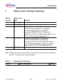
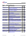
History List / Change Summary
1
History List / Change Summary
Table 2
History List
Version
Date
1.0
22.09.2008
1.1
04.12.2008
1.2
01.07.2009
Updated Documentation Reference:- TC1797 User’s Manual V1.1 2009-05
- TC1797 Data Sheet V1.1 2009-04
Removed BROM_TC.H001 (Frequency
RatiofSYS = fOSC/2 for Bootstrap Loaders), see
p.7-4 in TC1797 User’s Manual V1.1.
1.3
18.12.2009
Updated Documentation Reference:- TC1797 Data Sheet V1.2 2009-09.
Removed FLASH_TC.036 (DFLASH Margin
Control Register MARD), updated description
see p.5-69 in TC1797 User's Manual V1.1.
1.4
25.01.2011
Remark
Note: Changes to the previous errata sheet version are particularly marked in
column “Change” in the following tables.
Table 3
Errata fixed in this step
Errata
TC1797, QS-AC
Short Description
3/115
Change
Rel. 1.4, 25.01.2011
Errata Sheet
History List / Change Summary
Table 4
Functional Deviations
Functional
Deviation
Short Description
BCU_TC.006
Polarity of Bit SVM in Register ECON
13
BROM_TC.005
Power-on reset (PORST) while no external
clock is available
13
CPU_TC.105
User / Supervisor mode not staged
correctly for Store Instructions
13
CPU_TC.106
Incorrect PSW update for certain IP
instructions dual-issued with MTCR PSW
14
CPU_TC.107
SYSCON.FCDSF may not be set after FCD
Trap
15
CPU_TC.108
Incorrect Data Size for Circular
Addressing mode instructions with wraparound
16
CPU_TC.109
Circular Addressing Load can overtake
conflicting Store in Store Buffer
19
CPU_TC.110
Register Banks may be out of sync after
FCU Trap
22
CPU_TC.111
Imprecise Return Address for FCU Trap
24
CPU_TC.113
Interrupt may be taken during Trap entry
sequence
25
CPU_TC.114
CAE Trap may be generated by UPDFL
instruction
28
CPU_TC.115
Interrupt may be taken on exit from Halt
mode with Interrupts disabled
29
CPU_TC.117
Cached Store Data Lost on Data Cache
Invalidate via Overlay
DMA_TC.013
DMA-LMB-Master Access to Reserved
Address Location
33
DMI_TC.014
Problems with Parity Handling in TriCore
Data Memories
34
TC1797, QS-AC
4/115
Cha Pa
nge ge
New 31
Rel. 1.4, 25.01.2011
Errata Sheet
History List / Change Summary
Table 4
Functional Deviations (cont’d)
Functional
Deviation
Short Description
DMI_TC.015
LDRAM Access Limitations for 2KByte
Data Cache Configurations
35
DMI_TC.016
CPU Deadlock possible when Cacheable
access encounters Flash Double-Bit Error
36
DMI_TC.017
DMI line buffer is not invalidated by a write
to OVC_OCON.DCINVAL if cache off.
38
EBU_TC.020
BAA Delay Options Controlled by Wrong
Register Field
39
EBU_TC.021
Incorrect delay calculation accessing
Asynchronous memories
40
EBU_TC.022
Write Data Delay Control for
Asynchronous Memory Accesses
40
FADC_TC.005
Equidistant multiple channel-timers
41
FIRM_TC.010
Data Flash Erase Suspend Function
43
FLASH_TC.027
Flash erase time out of specification
FLASH_TC.035
Flash programing time out of specification
46
FlexRay_AI.056
In case eray_bclk is below eray_sclk/2,
TEST1.CERA/B may fail to report a
detected coding error
46
FlexRay_AI.062
Sync frame reception after noise or
aborted frame before action point
47
FlexRay_AI.064
Valid frame detection at slot boundary
47
FlexRay_AI.065
For sync nodes the error interrupt flag
EIR.SFO may be set too late
48
FlexRay_AI.066
Time stamp of the wrong channel may be
used for offset correction term
49
FlexRay_AI.067
Reception of more than gSyncNodeMax
different sync frames per double cycle
50
TC1797, QS-AC
5/115
Cha Pa
nge ge
Upd
ate
45
Rel. 1.4, 25.01.2011
Errata Sheet
History List / Change Summary
Table 4
Functional Deviations (cont’d)
Functional
Deviation
Short Description
FlexRay_AI.069
Update of Aggregated Channel Status ACS
in dynamic segment in minislots following
slot ID 2047
51
FlexRay_AI.070
Cycle counter MTCCV.CCV is updated
erroneously in dedicated startup states
51
FlexRay_AI.071
Faulty update of LDTS.LDTA, LDTB[10:0]
due to parity error
52
FlexRay_AI.072
Improper resolution of startup collision
53
FlexRay_AI.073
Switching from loop-back test mode at low
bit rate to normal active takes longer then
expected
53
FlexRay_AI.074
Integration successful on X and
integration abort on Y at the same point in
time leads to inconsistent states of SUC
and GTU
54
FlexRay_AI.075
Detection of parity errors outside
immediate scope
55
FlexRay_AI.076
CCSV.SLM [1:0] delayed to
CCSV.POCS[5:0] on transitions between
states WAKEUP and READY.
56
FlexRay_AI.077
Wakeup listen counter started one bit time
early
57
FlexRay_AI.078
Payload corruption after reception of valid
frame followed by slot boundary crossing
frame
57
FlexRay_AI.080
CLEAR_RAMS command does not clear
the 1st RAM word
58
FlexRay_AI.081
Write accesses to ERAY_NDIC* and
ERAY_MSIC* can fail if ERAY_CLC.FMC >=
2
59
TC1797, QS-AC
6/115
Cha Pa
nge ge
Rel. 1.4, 25.01.2011
Errata Sheet
History List / Change Summary
Table 4
Functional Deviations (cont’d)
Functional
Deviation
Short Description
FlexRay_AI.082
After detecting low level beyond
gdWakeupSymbolRxWindow, the node
may complete
59
FlexRay_AI.083
Irregular sync frame list exported in state
Coldstart_Gap
60
FlexRay_AI.084
Corruption of frame received in slot N by
second frame reception before action
point
61
FlexRay_AI.085
Cycle filtering in slot 1
62
FlexRay_AI.086
Bit IBFS of Register CUST1 always 0B
62
FlexRay_AI.088
A sequence of received WUS may
generate redundant SIR.WUPA/B events
63
FlexRay_AI.089
Rate correction set to zero in case of
SyncCalcResult=MISSING_TERM
64
FlexRay_AI.092
Initial rate correction value of an
integrating node is zero if
pMicroInitialOffsetA,B = 0x00
64
FlexRay_AI.093
Acceptance of startup frames received
after reception of more than
gSyncNodeMax sync frames
65
FlexRay_AI.094
Sync frame overflow flag EIR.SFO may be
set if slot counter is greater than 1024
66
FlexRay_AI.095
Register RCV displays wrong value
67
FlexRay_AI.096
Noise following a dynamic frame that
delays idle detection may fail to stop slot
67
FlexRay_AI.097
Loop back mode operates only at 10 MBit/s
68
FlexRay_AI.099
Erroneous cycle offset during startup after New 69
abort of startup or normal operation
FlexRay_AI.100
First WUS following received valid WUP
may be ignored
TC1797, QS-AC
7/115
Cha Pa
nge ge
New 70
Rel. 1.4, 25.01.2011
Errata Sheet
History List / Change Summary
Table 4
Functional Deviations (cont’d)
Functional
Deviation
Short Description
Cha Pa
nge ge
FlexRay_AI.101
READY command accepted in READY
state
New 70
FlexRay_AI.102
Slot Status vPOC!SlotMode is reset
immediately when entering HALT state
New 71
OCDS_AI.001
DAP restart lost when DAP0 inactive
71
OCDS_AI.002
JTAG Instruction must be 8 bit long
72
OCDS_TC.014
Triggered Transfer does not support half
word bus transactions
73
OCDS_TC.015
IOCONF register bits affected by
Application Reset
73
OCDS_TC.016
Triggered Transfer dirty bit repeated by
IO_READ_TRIG
74
OCDS_TC.018
Startup to Bypass Mode requires more
than five clocks with TMS=1
74
OCDS_TC.020
ICTTA not used by Triggered Transfer to
External Address
74
OCDS_TC.021
TriCore breaks on de-assertion instead of
assertion of break bus
75
OCDS_TC.024
Loss of Connection in DAP three-pin Mode
76
OCDS_TC.025
PC corruption when entering Halt mode
after a MTCR to DBGSR
77
OCDS_TC.026
PSW.PRS updated too late after a RFM
instruction.
77
OCDS_TC.027
BAM breakpoints with associated halt
action can potentially corrupt the PC.
79
OCDS_TC.028
Accesses to CSFR and GPR registers of
running program can corrupt loop exits.
PCP_TC.023
JUMP sometimes takes an extra cycle
81
PCP_TC.027
Longer delay when clearing R7.IEN before
atomic PRAM instructions
81
TC1797, QS-AC
8/115
New 80
Rel. 1.4, 25.01.2011
Errata Sheet
History List / Change Summary
Table 4
Functional Deviations (cont’d)
Functional
Deviation
Short Description
PCP_TC.032
Incorrect PCP behaviour following FPI
timeouts (as a slave)
82
PCP_TC.034
Usage of R7 requires delays between
operations
82
PCP_TC.035
Atomic PRAM operation right after
COPY/BCOPY
83
PCP_TC.036
Unexpected behaviour after failed posted
FPI write
83
PCP_TC.038
PCP atomic PRAM operations may operate Upd
ate
incorrectly
84
PCP_TC.039
PCP posted error interrupt to CPU may be
lost when the queue is full in 2:1 mode
85
RESET_TC.001
SCU_RSTSTAT.PORST not set by a
combined Debug / System / Application
Reset
86
SCU_TC.016
Reset Value of Registers ESRCFG0/1
87
SSC_AI.022
Phase error detection switched off too
early at the end of a transmission
87
SSC_AI.023
Clock phase control causes failing data
transmission in slave mode
88
SSC_AI.024
SLSO output gets stuck if a reconfig from
slave to master mode happens
88
SSC_AI.025
First shift clock period will be one PLL
clock too short because not syncronized
to baudrate
88
SSC_AI.026
Master with highest baud rate set
generates erroneous phase error
89
TC1797, QS-AC
9/115
Cha Pa
nge ge
Rel. 1.4, 25.01.2011
Errata Sheet
History List / Change Summary
Table 5
Deviations from Electrical- and Timing Specification
AC/DC/ADC
Deviation
Short Description
DTS_TC.P001
Test Conditions for Sensor Accuracy TTSA
90
FADC_TC.P003
Incorrect test condition specified in
datasheet for FADC parameter “Input
leakage current at VFAGND”.
90
MSC_TC.P001
Incorrect VOS limits for LVDS pads
specified in Data Sheet
New 90
PLL_TC.P005
PLL Parameters for fVCO > 780 MHz
91
Table 6
Cha Pa
nge ge
Application Hints
Hint
Short Description
ADC_AI.H002
Minimizing Power Consumption of an
ADC Module
92
CPU_TC.H004
PCXI Handling Differences in
TriCore1.3.1
92
CPU_TC.H005
Wake-up from Idle/Sleep Mode
EBU_TC.H005
Potential live-lock situation on
concurrent CPU and PCP accesses to
external memories
95
EBU_TC.H008
Use of EBU standby mode
95
EBU_TC.H009
Legal Parameters Allow an Invalid Page
Mode Access to be Configured
96
FIRM_TC.H000
Reading the Flash Microcode Version
97
FlexRay_AI.H002
Timer 1 Precision
97
FlexRay_AI.H003
Select upper-/lower page for IBF1/IBF2 in
RAM test mode
97
TC1797, QS-AC
10/115
Cha Pa
nge ge
New 94
Rel. 1.4, 25.01.2011
Errata Sheet
History List / Change Summary
Table 6
Application Hints (cont’d)
Hint
Short Description
Cha Pa
nge ge
FlexRay_AI.H004
Only the first message can be received in
External Loop Back mode
FlexRay_AI.H005
Initialization of internal RAMs requires
one eray_bclk cycle more
New 98
FlexRay_AI.H006
Transmission in ATM/Loopback mode
New 99
FlexRay_AI.H007
Reporting of coding errors via
TEST1.CERA/B
New 99
FlexRay_AI.H009
Return from test mode operation
New 99
FPI_TC.H001
FPI bus may be monopolized despite
starvation protection
GPTA_TC.H004
Handling of GPTA Service Requests
HYS_TC.H001
Effective Hysteresis in Application
Environment
104
MSC_TC.H007
Start Condition for Upstream Channel
104
MSC_TC.H008
The LVDS pads require a settling time
when coming up from pad power-down
state.
105
MSC_TC.H009
Incorrect MSC0 Interconnections
specified in User’s Manual V1.1.
98
100
New 100
New 106
MultiCAN_AI.H005 TxD Pulse upon short disable request
106
MultiCAN_AI.H006 Time stamp influenced by
resynchronization
106
MultiCAN_TC.H002 Double Synchronization of receive input
107
MultiCAN_TC.H003 Message may be discarded before
transmission in STT mode
107
MultiCAN_TC.H004 Double remote request
107
OCDS_TC.H001
108
TC1797, QS-AC
IOADDR may increment after aborted
IO_READ_BLOCK
11/115
Rel. 1.4, 25.01.2011
Errata Sheet
History List / Change Summary
Table 6
Application Hints (cont’d)
Hint
Short Description
OCDS_TC.H002
Setting IOSR.CRSYNC during Application
Reset
108
OCDS_TC.H003
Application Reset during host
communication
109
OCDS_TC.H004
Device Identification by Application
Software
110
PCP_TC.H004
Invalid parity error generated by FPI write
to PRAM
110
PCP_TC.H005
Unexpected parity errors when address 0
of CMEM is faulty
111
PCP_TC.H006
BCOPY address alignment error may
affect next channel FPI operation
111
PCP_TC.H007
Do not use priority 0 to post interrupt to
CPU
111
PORTS_TC.H004
Using LVDS Ports in CMOS Mode
112
PORTS_TC.H005
Pad Input Registers do not capture
Boundary-Scan data when BSD-mode
signal is set to high
112
PWR_TC.H005
Current Peak on VDDP during Power-up
112
SSC_AI.H001
Transmit Buffer Update in Slave Mode
after Transmission
113
SSC_AI.H002
Transmit Buffer Update in Master Mode
during Trailing or Inactive Delay Phase
114
SSC_AI.H003
Transmit Buffer Update in Slave Mode
during Transmission
114
SSC_TC.H003
Handling of Flag STAT.BSY in Master
Mode
115
TC1797, QS-AC
12/115
Cha Pa
nge ge
Rel. 1.4, 25.01.2011
Errata Sheet
Functional Deviations
2
Functional Deviations
BCU_TC.006 Polarity of Bit SVM in Register ECON
The polarity of bit SVM (State of FPI Bus Supervisor Mode Signal) in the SBCU
Error Control Capture register SBCU_ECON is inverted compared to its
description in the User’s Manual.
Actually, it is implemented as follows:
•
•
SVM = 0B: Transfer was initiated in user modes
SVM = 1B: Transfer was initiated in supervisor mode
BROM_TC.005 Power-on reset (PORST) while no external clock is available
In case no stable clock is present at the oscillator input pin (XTAL1) after
PORST, the device will wait indefinitely, i.e. it hangs and is not able to execute
application code or enter one of the bootstrap loader modes.
This behavior occurs only after PORST during initialization of the FlexRay
module by the internal Startup Software.
Workaround
Proper device start-up after PORST is only possible if a stable clock signal from
an external crystal, ceramic resonator or an external clock source is to available
at the XTAL1 pin of the device
CPU_TC.105 User / Supervisor mode not staged correctly for Store Instructions
Bus transactions initiated by TriCore load or store instructions have a number
of associated attributes such as address, data size etc. derived from the load or
store instruction itself. In addition, bus transactions also have an IO privilege
level status flag (User/Supervisor mode) derived from the PSW.IO bit field.
TC1797, QS-AC
13/115
Rel. 1.4, 25.01.2011
Errata Sheet
Functional Deviations
Unlike attributes derived from the instruction, the User/Supervisor mode status
of TriCore initiated bus transactions is not staged correctly in the TriCore
pipeline and is derived directly from the PSW.IO bit field.
This issue can only cause a problem in certain circumstances, specifically when
a store transaction is outstanding (e.g. held in the CPU store buffer) and the
PSW is modified to switch from Supervisor to User-0 or User-1 mode. In this
case, the outstanding store transaction, executed in Supervisor mode, may be
transferred to the bus in User mode (the bus systems do not discriminate
between User-0 and User-1 modes). Due to the blocking nature of load
transactions and the fact that User mode code cannot modify the PSW, neither
of these other situations can cause a problem.
Example
...
st.w [aX], dX
mtcr #PSW, dY
...
; Store to Supervisor mode protected SFR
; Modify PSW.IO to switch to User mode
Workaround
Any MTCR instruction targeting the PSW, which may change the PSW.IO bit
field, must be preceded by a DSYNC instruction, unless it can be guaranteed
that no store transaction is outstanding.
...
st.w [aX], dX
dsync
mtcr #PSW, dY
...
; Store to Supervisor mode protected SFR
; Modify PSW.IO to switch to User mode
CPU_TC.106 Incorrect PSW update for certain IP instructions dual-issued
with MTCR PSW
In certain situations where an Integer Pipeline (IP) instruction which updates the
PSW user status bits (e.g. PSW.V - Overflow) is followed immediately by an
MTCR instruction targetting the PSW, with the instructions being dual-issued,
TC1797, QS-AC
14/115
Rel. 1.4, 25.01.2011
Errata Sheet
Functional Deviations
the update priority is incorrect. In this case, the PSW user status bits are updated
with the value from the IP instruction rather than the later MTCR instruction.
This situation only occurs in 2 cases:
•
•
MUL/MADD/MSUB instruction followed by MTCR PSW
RSTV instruction followed by MTCR PSW
Example
...
rstv
mtcr #PSW, dY
...
; Modify PSW
Workaround
Insert one NOP instruction between the MUL/MADD/MSUB/RSTV instruction
and the MTCR instruction updating the PSW.
...
rstv
nop
mtcr #PSW, dY
...
; Modify PSW
CPU_TC.107 SYSCON.FCDSF may not be set after FCD Trap
Under certain conditions the SYSCON.FCDSF flag may not be set after an FCD
trap is entered. This situation may occur when the CSA (Context Save Area) list
is located in cacheable memory, or, dependent upon the state of the upper
context shadow registers, when the CSA list is located in LDRAM.
The SYSCON.FCDSF flag may be used by other trap handlers, typically those
for asynchronous traps, to determine if an FCD trap handler was in progress
when the another trap was taken.
Workaround
In the case where the CSA list is statically located in memory, asynchronous
trap handlers may detect that an FCD trap was in progress by comparing the
TC1797, QS-AC
15/115
Rel. 1.4, 25.01.2011
Errata Sheet
Functional Deviations
current values of FCX and LCX, thus achieving similar functionality to the
SYSCON.FCDSF flag.
In the case where the CSA list is dynamically managed, no reliable workaround
is possible.
CPU_TC.108 Incorrect Data Size for Circular Addressing mode instructions with wrap-around
In certain situations where a Load or Store instruction using circular addressing
mode encounters the circular buffer wrap-around condition, the first access to
the circular buffer may be performed using an incorrect data size, causing too
many or too few data bytes to be transferred. The circular buffer wrap-around
condition occurs when a load or store instruction using circular addressing
mode addresses a data item which spans the boundary of a circular buffer, such
that part of the data item is located at the top of the buffer, with the remainder
at the base. The problem may occur in one of two cases:
Case 1
Where a store instruction using circular addressing mode encounters the
circular buffer wrap-around condition, and is preceded in the LS pipeline by a
multi-access load instruction, the first access of the store instruction using
circular addressing mode may incorrectly use the transfer data size from the
second part of the multi-access load instruction. A multi-access load instruction
occurs in one of the following circumstances:
•
•
•
Unaligned access to LDRAM or cacheable address which spans a 128-bit
boundary.
Unaligned access to a non-cacheable, non-LDRAM address.
Circular addressing mode access which encounters the circular buffer wraparound condition.
Since half-word store instructions must be half-word aligned, and st.a
instructions must be word aligned, they cannot trigger the circular buffer wraparound condition. As such, this case only affects the following instructions using
circular addressing mode: st.w, st.d, st.da.
TC1797, QS-AC
16/115
Rel. 1.4, 25.01.2011
Errata Sheet
Functional Deviations
Example
...
LDA
LDA
LDA
...
ld.w
add
st.d
...
a8, 0xD000000E ; Address of un-aligned load
a12, 0xD0000820 ; Circular Buffer Base
a13, 0x00180014 ; Circular Buffer Limit and Index
d6, [a8]
; Un-aligned load, split 16+16
d4, d3, d2
; Optional IP instruction
[a12/a13+c], d0/d1 ; Circular Buffer wrap, 32+32
In this example, the word load from address 0xD000000E is split into 2 halfword accesses, since it spans a 128-bit boundary in LDRAM. The double-word
store encounters the circular buffer wrap condition and should be split into 2
word accesses, to the top and bottom of the circular buffer. However, due to the
bug, the first access takes the transfer data size from the second part of the unaligned load and only 16-bits of data are written. Note that the presence of an
optional IP instruction between the load and store transactions does not prevent
the problem, since the load and store transactions are back-to-back in the LS
pipeline.
Case 2
Case 2 is similar to case 1, and occurs where a load instruction using circular
addressing mode encounters the circular buffer wrap-around condition, and is
preceded in the LS pipeline by a multi-access load instruction. However, for
case 2 to be a problem it is necessary that the first access of the load instruction
encountering the circular buffer wrap-around condition (the access to the top of
the circular buffer) also encounters a conflict condition with the contents of the
CPU store buffer. Again, in this case the first access of the load instruction using
circular addressing mode may incorrectly use the transfer data size from the
second part of the multi-access load instruction. Since half-word load
instructions must be half-word aligned, and ld.a instructions must be word
aligned, they cannot trigger the circular buffer wrap-around condition. As such,
this case only affects the following instructions using circular addressing mode:
ld.w, ld.d, ld.da.
TC1797, QS-AC
17/115
Rel. 1.4, 25.01.2011
Errata Sheet
Functional Deviations
Note: In the current TriCore1 CPU implementation, load accesses are initiated
from the DEC pipeline stage whilst store accesses are initiated from the
following EXE pipeline stage. To avoid memory port contention problems
when a load follows a store instruction, the CPU contains a single store
buffer. In the case where a store instruction (in EXE) is immediately
followed by a load instruction (in DEC), the store is directed to the CPU
store buffer and the load operation overtakes the store. The store is then
committed to memory from the store buffer on the next store instruction or
non-memory access cycle. The store buffer is only used for store
accesses to ‘local’ memories - LDRAM or DCache. Store instructions to
bus-based memories are always executed immediately (in-order). A store
buffer conflict is detected when a load instruction is encountered which
targets an address for which at least part of the requested data is currently
held in the CPU store buffer. In this store buffer conflict scenario, the load
instruction is cancelled, the store committed to memory from the store
buffer and then the load re-started. In systems with an enabled MMU and
where either the store buffer or load instruction targets an address
undergoing PTE-based translation, the conflict detection is just performed
on address bits (9:0), since higher order bits may be modified by
translation and a conflict cannot be ruled out. In other systems (no MMU,
MMU disabled), conflict detection is performed on the complete address.
Example
...
LDA
LDA
LDA
...
st.h
ld.w
add
ld.d
a8, 0xD000000E ; Address of un-aligned load
a12, 0xD0000820 ; Circular Buffer Base
a13, 0x00180014 ; Circular Buffer Limit and Index
[a12]0x14, d7
; Store causing conflict
d6, [a8]
; Un-aligned load, split 16+16
d4, d3, d2
; Optional IP instruction
[a12/a13+c], d0/d1 ; Circular Buffer wrap, 32+32
; conflict with st.h
...
In this example, the half-word store is to address 0xD0000834 and is
immediately followed by a load instruction, so is directed to the store buffer. The
TC1797, QS-AC
18/115
Rel. 1.4, 25.01.2011
Errata Sheet
Functional Deviations
word load from address 0xD000000E is split into 2 half-word accesses, since it
spans a 128-bit boundary in LDRAM. The double-word load encounters the
circular buffer wrap condition and should be split into 2 word accesses, to the
top and bottom of the circular buffer. In addition, the first circular buffer access
conflicts with the store to address 0xD0000834. Due to the bug, after the store
buffer is flushed, the first access takes the transfer data size from the second
part of the un-aligned load and only 16-bits of data are read. Note that the
presence of an optional IP instruction between the two load transactions does
not prevent the problem, since the load transactions are back-to-back in the LS
pipeline.
Workaround
Where it cannot be guaranteed that a word or double-word load or store
instruction using circular addressing mode will not encounter one of the corner
cases detailed above which may lead to incorrect behaviour, one NOP
instruction should be inserted prior to the load or store instruction using circular
addressing mode.
...
LDA
LDA
LDA
...
ld.w
add
nop
st.d
...
a8, 0xD000000E ; Address of un-aligned load
a12, 0xD0000820 ; Circular Buffer Base
a13, 0x00180014 ; Circular Buffer Limit and Index
d6, [a8]
d4, d3, d2
; Un-aligned load, split 16+16
; Optional IP instruction
; Bug workaround
[a12/a13+c], d0/d1 ; Circular Buffer wrap, 32+32
CPU_TC.109 Circular Addressing Load can overtake conflicting Store in
Store Buffer
In a specific set of circumstances, a load instruction using circular addressing
mode may overtake a conflicting store held in the TriCore1 CPU store buffer.
The problem occurs in the following situation:
TC1797, QS-AC
19/115
Rel. 1.4, 25.01.2011
Errata Sheet
Functional Deviations
•
•
•
The CPU store buffer contains a byte store instruction, st.b, targeting the
base address + 0x1 of a circular buffer.
A word load instruction, ld.w, is executed using circular addressing mode,
targetting the same circular buffer as the buffered byte store.
This word load is only half-word aligned and encounters the circular buffer
wrap-around condition such that the second, wrapped, access of the load
instruction to the bottom of the circular buffer targets the same address as
the byte store held in the store buffer.
Additionally, one of the following further conditions must also be present for the
problem to occur:
•
•
The circular buffer base address for the word load is double-word but not
quad-word (128-bit) aligned - i.e. the base address has bits (3:0) = 0x8 with
the conflicting byte store having address bits (3:0) = 0x9, OR,
The circular buffer base address for the word load is quad-word (128-bit)
aligned and the circular buffer size is an odd number of words - i.e. the base
address has bits (3:0) = 0x0 with the conflicting byte store having address
bits (3:0) = 0x1.
In these very specific circumstances the conflict between the load instruction
and store buffer contents is not detected and the load instruction overtakes the
store, returning the data value prior to the store operation.
Note: In the current TriCore1 CPU implementation, load accesses are initiated
from the DEC pipeline stage whilst store accesses are initiated from the
following EXE pipeline stage. To avoid memory port contention problems
when a load follows a store instruction, the CPU contains a single store
buffer. In the case where a store instruction (in EXE) is immediately
followed by a load instruction (in DEC), the store is directed to the CPU
store buffer and the load operation overtakes the store. The store is then
committed to memory from the store buffer on the next store instruction or
non-memory access cycle. The store buffer is only used for store
accesses to ‘local’ memories - LDRAM or DCache. Store instructions to
bus-based memories are always executed immediately (in-order). A store
buffer conflict is detected when a load instruction is encountered which
targets an address for which at least part of the requested data is currently
held in the CPU store buffer. In this store buffer conflict scenario, the load
instruction is cancelled, the store committed to memory from the store
TC1797, QS-AC
20/115
Rel. 1.4, 25.01.2011
Errata Sheet
Functional Deviations
buffer and then the load re-started. In systems with an enabled MMU and
where either the store buffer or load instruction targets an address
undergoing PTE-based translation, the conflict detection is just performed
on address bits (9:0), since higher order bits may be modified by
translation and a conflict cannot be ruled out. In other systems (no MMU,
MMU disabled), conflict detection is performed on the complete address.
Example - Case 1
...
LDA
LDA
...
st.b
ld.w
...
a12, 0xD0001008 ; Circular Buffer Base
a13, 0x00180016 ; Circular Buffer Limit and Index
[a12]0x1, d2
; Store to byte offset 0x9
d6, [a12/a13+c] ; Circular Buffer wrap, 16+16
In this example the circular buffer base address is double-word but not quadword aligned. The byte store to address 0xD0001009 is immediately followed
by a load operation and is placed in the CPU store buffer. The word load
instruction encounters the circular buffer wrap condition and is split into 2 halfword accesses, to the top (0xD0001016) and bottom (0xD0001008) of the
circular buffer. The first load access completes correctly, but, due to the bug,
the second access overtakes the store operation and returns the previous halfword from 0xD0001008.
Example - Case 2
...
LDA
LDA
...
st.b
ld.w
...
a12, 0xD0001000 ; Circular Buffer Base
a13, 0x00140012 ; Circular Buffer Limit and Index
[a12]0x1, d2
; Store to byte offset 0x1
d6, [a12/a13+c] ; Circular Buffer wrap, 16+16
In this example the circular buffer base address is quad-word aligned but the
buffer size is an odd number of words (0x14 = 5 words). The byte store to
address 0xD0001001 is immediately followed by a load operation and is placed
TC1797, QS-AC
21/115
Rel. 1.4, 25.01.2011
Errata Sheet
Functional Deviations
in the CPU store buffer. The word load instruction encounters the circular buffer
wrap condition and is split into 2 half-word accesses, to the top (0xD0001012)
and bottom (0xD0001000) of the circular buffer. The first load access completes
correctly, but, due to the bug, the second access overtakes the store operation
and returns the previous half-word from 0xD0001000.
Workaround
For any circular buffer data structure, if byte store operations (st.b) are not used
targeting the circular buffer, or if the circular buffer has a quad-word aligned
base address and is an even number of words in depth, then this problem
cannot occur. If these restrictions and the other conditions required to trigger
the problem cannot be ruled out, then any load word instruction (ld.w) targeting
the buffer using circular addressing mode, and which may encounter the
circular buffer wrap condition, must be preceded by a single NOP instruction.
...
LDA
LDA
...
st.b
nop
ld.w
...
a12, 0xD0001000 ; Circular Buffer Base
a13, 0x00140012 ; Circular Buffer Limit and Index
[a12]0x1, d2
; Store to byte offset 0x1
; Workaround
d6, [a12/a13+c] ; Circular Buffer wrap, 16+16
CPU_TC.110 Register Banks may be out of sync after FCU Trap
In order to improve the performance of Upper Context Save and Restore
operations (Call, Interrupt etc.) the current TriCore1 CPU implementation
contains shadow registers for the upper context General Purpose Registers
(GPRs), D8-D15 and A10-A15, forming a foreground and a background bank.
In normal operation read and write accesses to the upper context registers
target the same bank, with read and write accesses targetting different banks
just during upper context save and restore operations.
However, in a certain corner case where an FCU trap is taken, read and write
accesses to the register banks remain out of synchronisation in the FCU trap
handler and cannot be easily re-synchronised. Since FCU traps are nonTC1797, QS-AC
22/115
Rel. 1.4, 25.01.2011
Errata Sheet
Functional Deviations
recoverable system errors, with some system state already lost, maintaining
correct behaviour is not critical. However, due to the bug, it is no longer straightforward to discriminate FCU traps from other context management (Class 3)
traps. Since the read and write pointers to the register banks are incorrect in the
bug situation, the update of D15 with the Trap Identification Number (TIN) will
write to one bank whilst the read of D15 in the trap handler will read the other
(incorrect) bank, returning an invalid TIN. For similar reasons, the upper context
GPRs are unusable in an FCU trap handler, since register read and write
operations may target different banks.
The problem occurs in the following situation:
•
•
•
FCX (Free Context Pointer) points to an invalid location (Null - End of CSA
list, Invalid Segment - Virtual or Peripheral segment).
CALL / CALLA / CALLI instruction is in the decode pipeline stage and would
generate an FCU trap due to the invalid FCX pointer.
Instruction in the Load-Store pipeline execute stage encounters a
synchronous trap condition (VAF-D, VAP-D, MPR, MPW, MPP, MPN, ALN,
MEM, DSE, SOVF, OVF), which would also be converted into an FCU trap.
Workaround
The LCX (Free Context List Limit) pointer should be initialised in order to trap
impending context list overflow before the FCU condition is encountered.
However, in order to maintain some system function in the case of an FCU trap,
the following workaround is required, split into two parts.
Firstly, the Context Management (Class 3) trap handler must be modified to
discriminate FCU traps that incorrectly appear to have a TIN pertaining to
another Class 3 trap due to the bug. This is done by checking for the correct
behaviour of the upper context registers and jumping to the FCU trap handler if
the register file behaviour is found to be in error:
_class3_handler:
mov d12, #7
nop
nop
jne d12, #7, _fcu_handler
mov d12, #-8
nop
TC1797, QS-AC
23/115
Rel. 1.4, 25.01.2011
Errata Sheet
Functional Deviations
nop
jne d12, #-8, _fcu_handler
; Now read valid D15 to obtain TIN
...
Since the initial contents of the upper context registers are unknown, it is
necessary to check one of the upper context registers twice, with different
values, in case the initial contents match the first value to be checked.
Note: The NOP instructions in the above code are mandatory to ensure that
reads from the GPRs target the register file directly, rather than the
forwarding paths which always function correctly.
Secondly, within the FCU trap handler itself, only the global and lower context
registers may be used, D0-D7 and A0-A9. Since the upper context information
is already lost in an FCU trap condition, usage of the global and lower context
registers without previously saving this information is acceptable.
CPU_TC.111 Imprecise Return Address for FCU Trap
The FCU trap is taken when a context save operation is attempted but the free
context list is found to be empty, or when an error is encountered during a
context save or restore operation. In failing to complete the context operation,
architectural state is lost, so the occurrence of an FCU trap is a non-recoverable
system error.
Since FCU traps are non-recoverable system errors, having a precise return
address is not important, but can be useful in establishing the cause of the FCU
trap. The TriCore1 CPU does not generate a precise return address for an FCU
trap if the cause of the FCU trap was one of the following trap types: FCD, DAE,
DIE, CAE or NMI.
In each of these circumstances the return address may be invalid.
Workaround
None
TC1797, QS-AC
24/115
Rel. 1.4, 25.01.2011
Errata Sheet
Functional Deviations
CPU_TC.113 Interrupt may be taken during Trap entry sequence
A problem exists whereby interrupts are not correctly disabled at the very
beginning of a trap entry sequence, and under certain circumstances an
interrupt may be taken at the start of a trap handler. The problem occurs when
an interrupt request is received by the TriCore CPU within a window spanning
a single clock cycle either side of a trap condition being detected, and where
interrupts are enabled and the interrupt priority number is higher than the
current CPU priority number (CCPN). In this case the trap entry sequence
begins and the upper context registers are stored to the appropriate CSA.
However, before the first instruction of the trap handler is executed the interrupt
condition is detected and the interrupt handler entered at a time when interrupts
should be disabled. This problem affects all trap types but does not affect
interrupts - an interrupt cannot be taken during the entry sequence of another
interrupt.
It should be noted that no state information is lost when this issue occurs. When
the interrupt handler completes and the RFE instruction is executed, program
execution restarts with the first instruction of the interrupted trap handler and the
trap handler then continues as normal.
The main issue associated with this problem is that the handling of the interrupt
will delay the start of the trap handler. For the majority of trap types associated
with the program flow this is not a problem. However, where the interrupted trap
type denotes a serious system problem, such as an NMI trap, the delay in
servicing the trap may be of concern. In addition, if interrupts are re-enabled
within the interrupt handler then the delay in returning to the trap handler will be
further extended by the handling of any additional higher priority interrupt
requests which may occur. However, once processing of the initial interrupt
handler is complete and the RFE instruction executed to return to the trap
handler, interrupts are correctly disabled immediately and the trap handler will
continue, even if further interrupts are pending when the RFE instruction is
executed.
Another point to note is that this issue can cause some assumptions made in
system software to be invalid. For example, if a system does not allow interrupts
or traps to re-enable interrupts - then it would have been safe to assume that
whenever a trap or interrupt is entered, that the code that has been suspended
(and hence the state information saved in the CSA) is for a user task and
TC1797, QS-AC
25/115
Rel. 1.4, 25.01.2011
Errata Sheet
Functional Deviations
typically non-privileged. Unfortunately, with this issue that premise no longer
holds - the code interrupted and state saved in a CSA can be that of a privileged
trap handler. Dealing with this changed circumstance is easy, provided it is
considered whenever CSA's are examined or manipulated.
Workaround
As described previously, the main problem associated with this erratum is the
delay that may be incurred before the servicing of certain critical trap types,
such as NMI, if no additional action is taken. If this is an issue for a system, then
in order to minimize the impact of this erratum it is necessary to adapt the
interrupt handlers to check for the occurrence of this issue and react
accordingly.
The occurrence of this issue may be checked for by one of two methods,
dependent upon whether all trap classes or just a limited set are considered
timing critical.
If it is required to check for the occurrence of this issue for all trap classes, then
this may be performed by checking the value of the PCXI.PIE register bit within
the interrupt handlers, before any further context operations (such as BISR) are
performed. If PCXI.PIE is clear, such that no interrupt should have been taken,
then this indicates the occurrence of this issue. Although when this method is
used then it is preferred to check the value of PCXI.PIE before any further
context operations are performed, it is possible to use this method after
additional context operations have been performed. In this case it is necessary
to traverse the CSA list to check the required PCXI.PIE value from the
appropriate saved context.
If it is necessary within a system to check for the occurrence of this issue just
for specific, timing critical, trap classes, then this may be performed by
examination of the return address, held in the A11 register, within the interrupt
handler and comparing this return address against the trap vector address(es).
For example, if only the NMI trap is a system issue requiring immediate action,
the following code may be added to the interrupt handler to determine if the
interrupt was taken at the start of the NMI handler:
...
< Timing critical section of Interrupt Handler >
movh.a a12, #@his(NMITrapAddress)
; BTV OR 0xE0
TC1797, QS-AC
26/115
Rel. 1.4, 25.01.2011
Errata Sheet
Functional Deviations
lea
a12, [a12]@los(NMITrapAddress) ; BTV OR 0xE0
eq.a
d13, a12, a11
; Compare with A11, result in d13
< Call / Branch to NMI handler based on d13 result >
Note that this code segment assumes that the BTV CSFR is static during
runtime. If this is not the case then it would be necessary to determine the trap
offset address during runtime by reading the BTV CSFR and ORing with the
TCN offset of the trap of interest. If more than one trap class is considered
timing critical within a system, it is possible to adapt the previous code to check
the return address of the interrupt handler against a number (or range) of trap
class entry addresses.
If the interrupted traps are considered recoverable, and are not time sensitive,
the interrupt handler can simply complete and it's terminating RFE will correctly
return execution to the first instruction of the trap handler - where it will now
execute to completion without undesired interruption. If the interrupted traps are
considered recoverable but are time sensitive and need to be executed
immediately, then some method of deferring the interrupt processing is
required. If the test of the situation (e.g. checking the PCXI.PIE bit is clear) is
at the start of the Interrupt handler, then there are two simple methods to
consider:
The first method would be to re-request the interrupt, by writing the appropriate
Service Request Control Register with the SETR bit set to one, and then
executing an RFE which will be taken back to the trap handler. The interrupt will
now be pending again, but will not be taken until the trap handler executes its
RFE to re-enable interrupts. This method is simple if the device (and hence it's
SRC register address) generating the interrupt is known. If this is not easy to
determine (statically or dynamically), the second method might be preferred.
The second method would be to jump to the trap handler, after setting the trap
identification number (TIN) and the return address (which the trap handler will
use) to be the next instruction in the interrupt handler. This relies on the fact that
the CSA saved away by the preemption of the trap handler is equally valid as
an execution context for the interrupt handler. The code for this method is as
follows:
interruptN:
mfcr
d15, PCXI
jnz.t d15, 23, interruptReal
TC1797, QS-AC
27/115
Rel. 1.4, 25.01.2011
Errata Sheet
Functional Deviations
; force CSA into memory
dsync
sh.h
d14, d15, #12
insert d15, d14, d15, #6, #16
mov.a a15, d15
; load trap value of d15 from CSA
ld.w
d15, [a15]0x3C
mov.a a15, a11
movh.a a11, #@his(interuptReal)
lea
a11, [a11]@los(interruptReal)
; jump to trap handler, will return to interruptReal
ji
a15
; the remaining part of the interrupt handler
interruptReal:
...
Again it is preferred that this method be used immediately at the beginning of
the interrupt handler, since this approach works straightforwardly provided
there is no state in the Upper Context registers or on the interrupt stack that is
required by the interrupt handler when it returned to. Although it is possible to
adapt this approach to operate later during interrupt handling, additional steps
need to be taken to ensure the correct state is maintained when returning to the
interrupt handler.
CPU_TC.114 CAE Trap may be generated by UPDFL instruction
UPDFL is a User mode instruction implemented as part of the TriCore1
Floating-Point Unit (FPU), which allows individual bits of the PSW user status
bits, PSW[31:24], to be set or cleared. Contrary to early revisions of the
TriCore1.3.1 architecture manual, and in contrast to most other FPU
instructions, the UPDFL instruction should not generate Co-Processor
Asynchronous Error (CAE) traps. However, in certain circumstances the
TriCore1.3.1 FPU will generate CAE traps for UPDFL instructions.
The TriCore1.3.1 FPU will generate a CAE trap upon execution of the UPDFL
instruction in the following situation:
TC1797, QS-AC
28/115
Rel. 1.4, 25.01.2011
Errata Sheet
Functional Deviations
•
•
•
After execution of the UPDFL instruction, one or more of the PSW[31:26]
bits are set - either the PSW bit(s) are set by UPDFL or were set prior to
execution and not cleared by the UPDFL instruction.
FPU traps are enabled for one of the asserted PSW[31:26] bits, via the
corresponding FPU_TRAP_CON.FxE bit being set.
The FPU_TRAP_CON.TST CSFR bit is clear - no previous FPU trap has
been generated without the subsequent clearing of FPU_TRAP_CON.TST.
Workaround
The UPDFL instruction is normally used in one of two situations:
•
•
Clearing the FPU sticky flags held in PSW[30:26].
Setting the FPU rounding mode bits in PSW[25:24].
In the first case, if all the PSW[31:26] bits are cleared by UPDFL, no CAE trap
will be generated.
In the second case, UPDFL may still be used to set the FPU rounding mode,
but in this case the remaining PSW bits, [31:26], must be cleared by UPDFL in
order to avoid generation of an unexpected CAE trap.
In all other cases, where FPU traps are enabled, some other method of
manipulating the PSW user status bits must be used in order to avoid
extraneous CAE trap generation. For instance, if in Supervisor mode the PSW
may be read using the MFCR instruction, the high order PSW bits modified and
written back using the MTCR instruction.
CPU_TC.115 Interrupt may be taken on exit from Halt mode with Interrupts disabled
A problem exists whereby an interrupt may be taken by the TriCore CPU upon
exiting Halt mode, even if interrupts are disabled at that point.
The problem occurs when an interrupt request is received by the TriCore CPU,
with the pending interrupt priority number (PIPN) higher than the current CPU
priority number (CCPN), and interrupts are enabled. In this case, where only the
CPU pipeline status is preventing the interrupt from being taken immediately,
the interrupt is latched and taken as soon as the pipeline can accept an
interrupt. This may cause unexpected behavior whilst debugging, where
TC1797, QS-AC
29/115
Rel. 1.4, 25.01.2011
Errata Sheet
Functional Deviations
interrupts are enabled before entry to Halt mode, or where interrupts are
temporarily enabled during Halt mode. In this case an interrupt may be latched
whilst the CPU is in Halt mode, and subsequently disabling interrupts during
Halt mode, by setting ICR.IE = 0B, will not prevent the interrupt from being
serviced immediately upon exit from Halt mode.
It should be noted that no corruption of the program flow is associated with this
issue and that it affects debugging only, primarily the debugger single-stepping
functionality. The problem may or may not be visible whilst debugging,
dependent upon the implementation of single-stepping by the debugger. If
single-stepping is implemented by the debugger setting Break-Before-Make
(BBM) breakpoints on all instructions except the next to be executed, then if this
problem occurs the next instruction when single-stepping will be the first
instruction of the interrupt handler. However, if single-stepping is implemented
by setting a Break-After-Make (BAM) breakpoint on the next instruction to be
executed, or a BBM breakpoint on the next but one instruction, the problem will
not be visible. In this case, when single-stepping, the interrupt handler will be
executed in its entirety before returning to the interrupted program flow and the
breakpoint being taken after the next instruction to be single-stepped.
Workaround
As described previously, this problem affects debug only and in this case the
taking of the interrupt immediately upon exit from Halt mode cannot be avoided
if the conditions to trigger the problem occur. However, the debugger singlestepping functionality may be implemented in such a way that this problem does
not directly affect the user, as follows:
Upon first hitting a breakpoint, the debugger should read and hold the current
interrupt enable status from ICR.IE. Interrupts should then be disabled by
setting ICR.IE = 0B.
If the next debugger action is to single-step, a BAM breakpoint should be placed
on the next instruction to be executed and the CPU re-started. In this case a
previously latched interrupt may be serviced, but will not result in a further
breakpoint being flagged until the interrupt handler returns and the next
instruction intended to be single-stepped is executed.
Subsequent single-step operations may be implemented using any appropriate
method, since interrupts will be disabled before Halt mode is entered.
TC1797, QS-AC
30/115
Rel. 1.4, 25.01.2011
Errata Sheet
Functional Deviations
If the debugger action is to re-start normal execution, the interrupt enable status
should be restored from the value read upon hitting the initial breakpoint and the
CPU re-started.
CPU_TC.117 Cached Store Data Lost on Data Cache Invalidate via Overlay
Cached store data can be lost if the overlay system requests a data cache
invalidate in the same cycle as a cache line is being written. The overlay control
provides a mechanism to do a single cycle invalidate of all valid/clean lines in
the data cache by writing the OCON.DCINVAL bit. Please note that there is no
problem if the data cache is used exclusively for read data (e.g. flash
constants).
Cache line state transition on DCINVAL.
valid/clean -> (DCINVAL) -> invalid/clean
A normal store operation transitions the cache line to a valid/dirty state.
Cache line state transition on normal store operation.
valid/clean -> (write) -> valid/dirty
invalid/clean -> (write) -> valid/dirty
In the case where the write and invalidate are received in the same cycle, the
dirty bit is correctly updated but the valid bit is incorrectly cleared.
Cache line state transition on store operation with DCINVAL
valid/clean -> (write+DCINVAL)- > invalid/dirty
invalid/clean -> (write+DCINVAL) -> invalid/dirty
This leads to a loss of data as the store data ends up being held in an invalid
cache line and hence never re-read.
Workaround-1
Ensure that the data cache is never used to cache write data. This can be
ensured by software design but may limit performance in some systems.
TC1797, QS-AC
31/115
Rel. 1.4, 25.01.2011
Errata Sheet
Functional Deviations
Workaround-2
Ensure that the core is never storing data when OCON.DCINVAL is asserted.
This requires the CPUs store buffers to be empty when the invalidate is
asserted. This can only be done by getting the CPU to firstly flush all write data
with a DSYNC command, then to write the OCON.DCINVAL to trigger an
invalidate.
The following example code sequence performs the required operations:•
•
•
•
•
Read the OCON register to get the current SHOVEN field
Create a new OCON value with DCINVAL, OVSTRT and OVCONF bits set
Perform a DSYNC operation to flush all write data to memory
Write OCON with the new value.
Read back OCON to ensure write is complete
;; Set up A14 with address of OCON Register
movh.a a14,#(((0xF87FFBE0)+0x8000>>16) & 0xffff)lea
a14,[a14]((((0xF87FFBE0)+0x8000)&0xffff)-0x8000)
;; Load a15 with contents of OCON
ld.w
d15, [a14]
;; Set OCONF, DCINVAL, OVSTRT start values
movh
d14 , #0x0305
;; Combine existing SHOVEN
insert d15, d14,d15,#0,#16
; Flush all store data
dsync
;; Store New value back to OCON
st.w
[a14], d15
;; Re-read to ensure store is complete
ld.w
d15, [a14]
Attention: This routine must be run with interrupts disabled, either as part
of an interrupt service routine or guarded by enable/disable
instructions.
This routine may be run periodically or run as part of a dedicated interrupt
service routine. If the latter approach is used it is suggested that an unused
TC1797, QS-AC
32/115
Rel. 1.4, 25.01.2011
Errata Sheet
Functional Deviations
SRN either in the CPU or Cerberus is utilised to trigger the invalidate. In all
cases the routine must be run with interrupts disabled to ensure that no writes
are in progress when the invalidate occurs.
The OCON.OVCONF bit may be used to indicate the state of the invalidate
operation. If it is cleared in advance, the routine above will set it when the cache
invalidate operation is performed.
DMA_TC.013 DMA-LMB-Master Access to Reserved Address Location
DMA-LMB-Master goes into an unintentional lock-up state when a Read or
Write access is made to a reserved memory location with an unrecognised
slave.
Subsequent Read/Write accesses from a DMA Channel, MLI, Cerberus or the
DMA-FPI-Slave to all memory locations mapped to the DMA-LMB-Master
(80000000H to DFFFFFFFH) will be halted until control of the DMA-LMB-Master
is regained.
In the case of a lock-up DMA-LMB-Master Read access, the next LMB access
and associated response will have the following effect:
•
•
•
ERROR Response: The DMA-LMB-Master will treat this error response as
its own. It will clear the lock-up state and return an error to the DMA access
requester. Normal operation will then continue. Halted DMA access
requests will resume. There is no corruption of the data flow.
NSC (No Special Condition) Acknowledge: The DMA-LMB-Master will treat
this response as its own and again clear the lock-up state. The correct
response to an unrecognised slave is an ERROR. Therefore the DMA-LMBMaster has signalled an invalid response back to the DMA access requester
resulting in a corruption of the data flow.
RETRY Response: The DMA-LMB-Master will treat the retry response as its
own and again clear the lock-up state. The access will be repeated to the
same reserved address location again resulting in a lock-up condition. The
sequence is broken by the first ERROR response or NSC acknowledge.
The effect of a DMA-LMB-Master Write accesses to an unrecognised slave is
the same as above with one exception:
TC1797, QS-AC
33/115
Rel. 1.4, 25.01.2011
Errata Sheet
Functional Deviations
•
If the next access is a Read access from the EBU-LMB-Slave then the DMALMB-Master will clear the lock-up state and respond as above. The EBU
read completes but the data read by the Originator (e.g. TriCore) will be the
write data of the DMA-LMB-Master Write access.
The following should be noted:
•
•
At all times the DMA-FPI-Master and DMA-FPI-Slave remain accessible.
If the LMB-DMA-Master is in the lock-up state then accesses can still be
made to the LMB bus by all other LMB-Masters (e.g. LFI-LMB-Master).
Hint
Do not perform a DMA channel, MLI, Cerberus or DMA-FPI-Slave access to a
reserved address: all areas specified as reserved in the Memory Map Chapter,
LMB Address Map Table must not be accessed by the DMA (ME, MLI,
Cerberus).
Workaround
The LMB-Bus-Control-Unit can recognise a DMA-LMB-Master access to an
unrecognised slave. It can be programmed to raise an interrupt and then
generate a Class 3 Application Reset to clear the lock-up state.
DMI_TC.014 Problems with Parity Handling in TriCore Data Memories
A small number of cases exist in which the handling of parity errors in the
TriCore data memories (LDRAM, DCache and Data Cache Tag) does not
function correctly, potentially leading to data corruption for accesses to these
memories. This data corruption may occur whether the access to one of these
memories is from the TriCore CPU, or, in the case of LDRAM, from another bus
master access via the LMB.
Workaround
In systems where the Data Memory parity handling must be enabled, the
following is required to guarantee correct behaviour:
•
Compatibility mode must be selected for the TriCore Data side memories by
setting COMPAT.DIE = 1B. In this case parity errors are signalled to the SCU
TC1797, QS-AC
34/115
Rel. 1.4, 25.01.2011
Errata Sheet
Functional Deviations
and returned to the CPU as an NMI trap, rather than as a DIE trap directly
to the CPU.
AND
•
If the system has a data cache, the data cache must be used to cache readonly data only (such as Flash contents). Writes to cacheable locations must
not be used with the Data Cache enabled.
Note that this does not concern the program side which works as expected.
DMI_TC.015 LDRAM Access Limitations for 2KByte Data Cache Configurations
TriCore1.3.1 based devices are physically built with a certain size of Data
Memory (DMEM) and a data tag memory to support a certain maximum size of
Data Cache (DCache). Within these physical limitations, software may select
the exact split between LDRAM and DCache where DMEM size = LDRAM size
+ DCache size. The software selection is performed according to the
configuration of the DCache size in DMI_CON.DC_SZ_CFG, with any DMEM not
configured as DCache ordinarily available as LDRAM.
However, a problem exists where the DCache is configured to be 2KByte,
DMI_CON.DC_SZ_CFG = 0001B. In this case the expected amount of LDRAM
is available for accesses from the CPU (DMEM size - 2KByte), but the address
range checking is incorrect for accesses to LDRAM from the LMB and the
available LDRAM size for LMB accesses is limited to (DMEM size - 4KByte).
Example
A TC1767 device is physically built to support a maximum of 72KByte DMEM
and 4KByte DCache. Where the DCache size is configured as 4KByte,
available LDRAM is 68KByte, where the DCache size is configured as 0KByte,
available LDRAM is 72KByte. However, when the DCache size is configured as
2KByte, 70KByte LDRAM is addressable by the CPU, but only the bottom
68KByte is addressable by LMB bus masters.
TC1797, QS-AC
35/115
Rel. 1.4, 25.01.2011
Errata Sheet
Functional Deviations
Workaround
In systems where a 2KByte DCache is configured, the top 2KByte of LDRAM is
only available for usage by the CPU, and cannot contain data structures that
may be required by other bus masters. For instance, this space could be used
as part of the CSA list. However, note that since this memory is not addressable
by LMB masters in the 2KByte DCache configuration, this would affect
debuggers. Hence it would only be possible to view this memory space in a
debugger if it takes appropriate steps to make the memory region accessable
(e.g. by temporarily setting the DCache size to 0KByte) to examine that address
range.
DMI_TC.016 CPU Deadlock possible when Cacheable access encounters
Flash Double-Bit Error
A problem exists whereby the TriCore CPU may become deadlocked when
attempting a mis-aligned load access to a cacheable address. The problem will
be triggered in the following situation:
•
•
•
•
The TriCore CPU executes a load instruction whose target address is not
naturally aligned - a data word access which targets an address which is not
word aligned, or a data / address double-word access which is not doubleword aligned.
The mis-aligned load access targets a cacheable address, whether the
device is configured with a data cache or not.
The mis-aligned load access spans two halves of the same 128-bit cache
line. For instance, a data word access with address offset 6H.
The mis-aligned load access results in a cache miss, which will refill the 128bit cache line / Data Line Buffer (DLB) via a Block Transfer 2 (BTR2) read
transaction on the LMB, and this LMB read encounters a bus error condition
in the second beat of the block transfer.
It should be noted that under normal operation, LMB block transfers will not
result in a bus error condition being flagged on the second beat of a block
transfer. However, such a condition may be encountered when accessing the
on-chip Flash, if the second double-word of data accessed from the Flash (for
the second half of the cache line) contains an uncorrectable double-bit error.
TC1797, QS-AC
36/115
Rel. 1.4, 25.01.2011
Errata Sheet
Functional Deviations
When this condition is triggered, the first part of the requested data is obtained
from the valid first beat of the BTR2 transfer, and the second part is required
from the errored second beat. In this case, no error is flagged to the TriCore
CPU and the transaction is incorrectly re-started on the LMB. In the case of a
Flash double-bit error, this transaction will be re-tried continuously on the LMB
by the DMI LMB master and the CPU become deadlocked. This situation would
then only be recoverable by a Watchdog reset.
The problem exists within the DMI DLB, which is used as a single cache line
when no data cache is configured, and as a streaming buffer when data cache
is present. As such the problem affects all load accesses to cacheable
locations, whether data cache is configured or not, since the DLB is used in both
cases.
Note: This problem affects load accesses to the on-chip Flash only. Instruction
fetches which encounter a similar condition (bus error on later beat of
block transfer) behave as expected and will return a PSE trap upon any
attempt to execute an instruction from a Flash location containing a
double-bit error.
Workaround
As described previously, this problem should not be encountered during normal
operation and will only be triggered in the case of a double-bit error being
detected in an access to the on-chip Flash.
However, in order to remove the possibility of encountering this issue, all load
accesses to cacheable addresses within the on-chip Flash should be made
using natural alignment - word transfers should be word aligned, double-word
transfers double-word aligned.
It is also possible to check for the occurrence of this problem by having some
other master, such as the PCP, periodically poll the LBCU LEATT register to
check for the occurrence of LMB error conditions, specifically if one is detected
during a BTR2 read transfer from the DMI, as reported by LEATT.OPC and
LEATT.TAG.
TC1797, QS-AC
37/115
Rel. 1.4, 25.01.2011
Errata Sheet
Functional Deviations
DMI_TC.017
DMI line buffer
is not invalidated by a write to
OVC_OCON.DCINVAL if cache off.
A problem exists whereby the DMI line buffer is not invalidated by a write to
OVC_OCON.DCINVAL when operating with the D-cache turned off. This
means that the user cannot rely on a write to OVC_OCON.DCINVAL to make
sure that any stale data in the DMI line buffer is invalidated. This can be a
problem for users who want to use the OVC_OCON.DCINVAL bit to ensure
coherency between the DMI and background memory.
It should be noted that this problem is not encountered when the D-cache is
turned on. When the D-cache is turned on, writing a one to
OVC_OCON.DCINVAL will correctly invalidate all clean cache entries and
invalidate the DMI line buffer. The problem only concerns systems with no
cache or systems where the cache is turned off.
Detailed description
D-Cache turned on:
When D-cache is turned on, the DMI line buffer is only used as a performance
enhancement mechanism with no logical existence to the user. It is therefore
not operating as a micro-cache and the current issue does not apply. When the
dcache is turned on, writing to OVC_OCON.DCINVAL will always invalidate all
clean lines in the dcache. No stale data will subsist in the DMI line buffer.
D-Cache turned off:
The problem occurs when the dcache is turned off. When the dcache is turned
off (or non-existent) the DMI line buffer operates as a 16-byte cache. Writing a
one to the OVC_OCON.DCINVAL register should invalidate the data inside the
DMI line buffer as long as the data is not dirty. This invalidation mechanism
does not work on AUDO-Future devices. Writing to OVC_OCON.DCINVAL will
have no effect at all. Any cache line which was previously loaded into the DMI
line buffer will not be invalidated (whether it was dirty or not).
Workaround
The workaround consists in executing a cachei.wi instruction with an operand
register containing a random non-protected cacheable address. The DMI line
buffer will respond to cachei.wi instructions regardless of the content of its
TC1797, QS-AC
38/115
Rel. 1.4, 25.01.2011
Errata Sheet
Functional Deviations
operand, provided that the operand contains a cacheable address which is not
protected. On execution of cachei.wi, the DMI line buffer will flush and invalidate
itself. For example, executing the following two instructions should flush and
invalidate the DMI line buffer in any circumstance. Note that the current
workaround always invalidates the entry regardless of whether it was dirty or
not.
movh.a a0, #0x8000 ;; Cachei operand is random nonprotected cacheable address.
cachei.wi [a0]
;; The DLB gets invalidated regardless
of the value in a0.
If the user is not concerned in invalidating the DMI line buffer but simply
guaranteeing its coherency with external memory then there is another simple
workaround. This consists in issueing a read to a dummy cacheable address
pointing outside the 16-byte block containing the next required data. Access to
the next required data will then necessarily result in a refill and the resulting data
will be coherent. This is what the following code does (a0 contains a dummy
address and a1 contains the address for the user's required data).
movh.a a0, #0x8000 ;; Dummy address is 0x80000000.
ld.w d0, [a0]
;; a0 has to point to different 16-byte
block than a1.
ld.w d0, [a1]
;; This load will be executed fresh from
memory with a refill.
;; Read data will be coherent with rest
of memory.
EBU_TC.020 BAA Delay Options Controlled by Wrong Register Field
The timing options for the BAA signal are specified as being controlled by the
settings of the BUSRCONx.EXTCLOCK and BUSRCONx.EBSE register fields.
In the implementation of the EBU, the logic controlling BAA timing was
connected to the BUSRCONx.ECSE field instead of BUSRCONx.EBSE.
TC1797, QS-AC
39/115
Rel. 1.4, 25.01.2011
Errata Sheet
Functional Deviations
Workaround
Use the BUSRCONx.ECSE field to control the desired timing option for the BAA
signal.
EBU_TC.021 Incorrect delay calculation accessing Asynchronous memories
The EBU has the facility for the flash clock to run continuously by setting one of
the BUSRCONx.BFCMSEL to 0B. In this case, as all attached devices see the
same clock, then all accesses requiring a flash clock will use the
BUSRAPx.EXTCLOCK
setting
from
the
region
which
has
BUSRCONx.BFCMSEL =0B when determining the correct delays for the
various control signals enabled by the ECSE and EBSE bits.
However, no distinction was made for asynchronous regions to enable them to
use a separate method of delay calculation so, if a continuous flash clock is
enabled, signal delays for asynchronous accesses will be calculated using the
same EXTCLOCK value as that used for synchronous accesses instead of the
EXTCLOCK value in the registers of the region being accessed.
Workaround
If the continuous flash clock mode is in use, adjust the phase lengths for the
asynchronous regions to compensate for the modified signal delays.
EBU_TC.022 Write Data Delay Control for Asynchronous Memory Accesses
The EBU allows the timing of the write data driven onto the EBU_AD(31:0) pins
to
be
adjusted
using
the
EBU_BUSWCONx.ECSE
and
EBU_BUSWAPx.EXTCLOCK register fields. This delay mechanism is not
working as specified for asynchronous write accesses:
•
The time at which write data is disabled cannot be delayed by half a clock
cycle. Register settings where a half clock cycle delay would be expected
will result in a full clock cycle of delay.
TC1797, QS-AC
40/115
Rel. 1.4, 25.01.2011
Errata Sheet
Functional Deviations
•
•
The time at which write data is enabled is never delayed. The bus will always
be driven as if no delay was in effect. If the register settings require the data
to be delayed then invalid data will be driven for the delay period.
The time at which valid write data is driven cannot be delayed by half a clock
cycle. Register settings where a half clock cycle delay would be expected
will result in no delay being applied.
This results in the timing detailed in the table below, where CP1 is the first clock
cycle of the command phase, DHn is the last clock cycle of the Data Hold Phase
and TCLK is one period of the EBU clock:
Table 7
Write Data Signal Timing
EXTCLOCK is set to
Driven at:
Delay
Disabled
Removed at:
Delay
Enabled
Delay
Disabled
Delay
Enabled
End of DHn
+ TCLK
00B
Start of
CP1
Start of
CP1
End of
DHn1)
01B, 10B, 11B
Start of
CP1
End of
CP12)
End of DHn End of DHn
+ TCLK
1) DHn indicates the final Data Hold Phase. If no Data Hold is programmed, this will
be CPn, the final Command Phase.
2) Data bus will be enabled at the beginning of CP1
Workaround
Adjust the phase lengths for the asynchronous regions to compensate for the
modified signal delays.
FADC_TC.005 Equidistant multiple channel-timers
The description is an example for timer_1 and timer_2, but can also affect all
other combinations of timers.
Timer_1 and Timer_2 are running with different reload-values. Both timers
should start conversions with the requirement of equidistant timing.
Problem description:
TC1797, QS-AC
41/115
Rel. 1.4, 25.01.2011
Errata Sheet
Functional Deviations
Timer_1 becomes zero and starts a conversion. Timer_2 becomes zero during
this conversion is running and sets the conversion-request-bit of channel_2. At
the end of the conversion for channel_1 this request initiates a start for
channel_2. But the Timer_2 is reloaded only when setting the request-bit for
channel_2 and is decremented during the conversion of channel_1.
The correct behavior would be a reload when the requested conversion (of
channel_2) is started.
Therefore the start of conversion for channel_2 is delayed by maximum one
conversion-time. After this delay it will be continued with equidistant conversionstarts. Please refer to the following figure.
R = T im e r lo a d e d w ith R e lo a d -v a lu e
0 = T im e r b e c o m e s z e ro
T im e r_ 1
DECD
R E0C R
R
0 R
DECR
0 R
S ta rt_ c h a n 1
B usy1
c o n v e rs io n tim e
1 .) In h a rd w a re im p le m e n te d fe a tu re
T im e r_ 2
DECR
0 R
DECR
0 R
DECR
0 R
DECR
0 R
DECR
0 R
S ta rt_ c h a n 2
S ta rt s h ifte d
p ro g r. tim e r ra te
p ro g r. tim e r ra te
0 R
0 R
2 .) S p e c c o m fo rm fe a tu re
T im e r_ 2
DECR
0 R
DECR
0
S ta rt s h ifte d
R
DECR
p ro g . tim e r ra te
DECR
p ro g . tim e r ra te
N o te : th e p ro g ra m m e d tim e r ra te is m u c h lo n g e r th a n th e c o n v e rs io n tim e ,
th is m e a n s th a t th e fa u lt is m u c h s m a lle r th a n in th e p ic tu re
Figure 1
Timing concerning equidistant multiple timers
TC1797, QS-AC
42/115
Rel. 1.4, 25.01.2011
Errata Sheet
Functional Deviations
Workaround
Use one timer base in combination with neighboring trigger and selection by
software which result has to be taken into account.
FIRM_TC.010 Data Flash Erase Suspend Function
This problem affects devices with microcode version V11 (see FIRM_TC.H000
for identification of the microcode version):
A sector DFx in the Data Flash may not be correctly erased when two
successive erase operations are executed without any programming between
the erase operations, as described in the following sequence (x, y = 0 or 1,
x ? y):
1. A Program Flash sector or a Data Flash sector (DFy or DFx) has been
erased.
2. An erase command on Data Flash sector DFx is issued.
3. While the erase operation on sector DFx is in progress, during a certain
critical time window a programming command on sector DFy is issued, i.e.
the erase operation on sector DFx is suspended.
In other words, potentially critical sequences are:
•
•
•
Erase PFLASH --> erase DFx --> program DFy (suspend erase DFx), or
Erase DFy --> erase DFx --> program DFy (suspend erase DFx), or
Erase DFx --> erase DFx --> program DFy (suspend erase DFx).
As a consequence, sector DFx may not be correctly erased after the suspended
erase has been completed (i.e. DFx may be weakly programmed). The effect is
non-permanent, i.e. erasing DFx again will solve the issue.
Note: Sector DFy is always correctly programmed.
Therefore, both Data Flash sectors or a Program and a Data Flash sector must
not be erased one after the other if the second erase operation might be
suspended.
Workaround 1
Additionally program (a page of) Data Flash sector DFx or DFy, before starting
the erase of DFx, e.g.:
TC1797, QS-AC
43/115
Rel. 1.4, 25.01.2011
Errata Sheet
Functional Deviations
1. Erase PFLASH or DFx or DFy
2. Additional step: Program DFx or DFy (specified rules for Data Flash page
programming must remain valid), check for completion of programming
(busy)
3. ... (any operation except erase of DFx, DFy, or PFLASH)...
4. Erase DFx
5. Concurrent programming of DFy may be triggered.
Workaround 2
After starting the erase of Data Flash sector DFx, delay the start of the
programing of sector DFy by at least 250 ms, e.g.:
1. Erase DFx
2. Additional step: Wait > 250 ms
3. Concurrent programming of DFy may be triggered.
Workaround 3
Issue a reset in case of two consecutive erase operations without intermediate
programming, e.g.:
1.
2.
3.
4.
5.
Erase DFx
Erase DFy
Additional step: Reset
Erase DFx (if needed)
Concurrent programming of DFy may be triggered.
Workaround 4
After a concurrent erase on Data Flash sector DFx has been triggered, verify
the state of DFx.
In case of weak programming, re-erase DFx (Additional step).
Workaround 5
Do not use concurrent erase/program operations on Data Flash.
TC1797, QS-AC
44/115
Rel. 1.4, 25.01.2011
Errata Sheet
Functional Deviations
FLASH_TC.027 Flash erase time out of specification
As per specification in the Data Sheet following are the flash erase timings:
Table 8
Flash erase timings as per spec.
Flash
Micro
code
version
Erase Time
P-Flash, 2 MByte
V11
40s [at cold and room
temperature]
D-Flash, 64 Kbyte [Both
Data Flash]
V11
2.5s [at cold temperature]
Actual Flash erase timings may reach the following maximum values. A
minimum erase time budget per erase operation of 0.5 s must however be
tolerated regardless of size-proportional erase times derived from the table.
Table 9
Actual Flash erase timings.
Flash
Micro
code
version
Erase Time
P-Flash, 2 MByte
V11
52s [at cold temperature]
45s [at room and above
temperature]
D-Flash, 64 Kbyte [Both
Data Flash]
V11
3.2s [at all temperature]
Maximum erase time at various CPU operating frequencies can be calculated
according to the following table. Frequency dependency for Data Flash is lower
than for Program Flash.
TC1797, QS-AC
45/115
Rel. 1.4, 25.01.2011
Errata Sheet
Functional Deviations
Table 10
Relative erase time increments.
Frequency [MHz]
Increment for P-Flash
Increment for D-Flash
80
8%
5%
100
5%
3%
133
2%
1.5%
150
1%
1%
180
0%
0%
FLASH_TC.035 Flash programing time out of specification
As per specification flash programing time specified is per page 5msec
Where as actual programing time measured on the device is per page 5.5msec
FlexRay_AI.056 In case eray_bclk is below eray_sclk/2, TEST1.CERA/B
may fail to report a detected coding error
Description:
All detected coding errors should be reported in the Test Register 1, at
TEST1.CERA/ CERB. If eray_bclk is below eray_sclk/2, it may happen,
depending on phase difference of eray_bclk and eray_sclk, that TEST1.CERA/
CERB are not updated in case of a detected coding error and remain in the state
0000B = "No coding error detected".
Scope:
The erratum is limited to the case where eray_bclk is below eray_sclk/2.
Effects:
Coding errors not reported via TEST1.CERA/ CERB. The frame decoding is not
affected.
TC1797, QS-AC
46/115
Rel. 1.4, 25.01.2011
Errata Sheet
Functional Deviations
Workaround
None.
FlexRay_AI.062 Sync frame reception after noise or aborted frame before
action point
Description:
In case noise or an aborted frame leads to the detection of a secondary time
reference point (STRP) and after this a valid sync frame is detected in the same
slot and the STRP of the valid sync frame occures simultanoeusly with the
action point, the temporal deviation value of the first detected STRP is stored
instead of the value of the correct STRP.
Scope:
The erratum is limited to the case of noise before reception of a valid sync frame
or a frame reception starting before action point is aborted and then a valid sync
frame is received in the same slot.
Effects:
In the described case a wrong deviation value is used for correction term
calculation. Depending on number of sync frames and other measured
temporal deviation values it may lead to an incorrect rate or offset correction
value.
Workaround
None.
FlexRay_AI.064 Valid frame detection at slot boundary
Description:
In case a non sync frame is detected to be valid simultaneously with the slot
boundary and in the following slot a sync frame is received, the temporal
TC1797, QS-AC
47/115
Rel. 1.4, 25.01.2011
Errata Sheet
Functional Deviations
deviation value (= time between primary time reference point and action point)
of the received sync frame is erroneously set to the measured value of the
previous non sync frame.
Scope:
The erratum is limited to the case where a non sync frame is received in one
slot and a sync frame is received in the following slot. Additionally, the detection
of valid frame for the non sync frame has to be exactly at the slot boundary.
Effects:
The temporal deviation value of the sync frame is set to the deviation value of
the previous non sync frame. The positive shift of the non sync frame in
direction of slot end results in a relative large positive deviation value (order of
magnitude of the parameter gdActionPointOffset). With more than two sync
frame senders within the cluster, this large value is most probably not taken into
account for correction term calculation because of the nature of the faulttolerant midpoint algorithm.If the faulty value is used for offset correction term
calculation, the resulting offset shift will be corrected in the following cycles.
Workaround
None.
FlexRay_AI.065 For sync nodes the error interrupt flag EIR.SFO may be
set too late
Description:
The E-Ray acting as sync node does not consider its own sync frame for
counting number of sync frames. Thus it sets the error interrupt flag EIR.SFO
if it receives more than gSyncNodeMax (GTUC2.SNM[3:0]) sync frames.
Scope:
TC1797, QS-AC
48/115
Rel. 1.4, 25.01.2011
Errata Sheet
Functional Deviations
The erratum is limited to the case where a sync node receives exactly
gSyncNodeMax sync frames from other sync nodes during one communication
cycle.
Effects:
In the described case error interrupt flag EIR.SFO is not set.
Workaround
Avoid faulty configurations with more than gSyncNodeMax nodes configured to
be transmitter of sync frames.
FlexRay_AI.066 Time stamp of the wrong channel may be used for offset
correction term
Description:
In case the temporal deviation (= time between primary time reference point and
action point offset) is different for channel A and B and the values have the
following combination
•
•
greater than or equal zero on one channel and negative on the other
channel
the channel with a relative deviation value greater than or equal zero is
choosen for offset correction term calculation instead of the negative value.
Scope:
The erratum is limited to the case where both channels are used and if there is
a large difference in the propagation delays on channel A and B.
Effects:
In case of the described relation between measured deviation values on
channel A and B the calculated offset correction term may have an error of
maximum the difference between the two deviation values. Thus, the error of
the local time of the node is limited to the difference of the temporal deviation
values of both channels.
TC1797, QS-AC
49/115
Rel. 1.4, 25.01.2011
Errata Sheet
Functional Deviations
Workaround
For dual channel FlexRay systems sync frames have to be transmitted on both
channels. In practice, the propagation delay between two nodes is expected to
be nearly the same on both channels. If this is not the case, the channel
depending parameter pDelayCompensation[A/B] (GTUC5.DCA, DCB) has to be
used to compensate the different propagation delays. With a correct adjustment
of the parameter the difference of the deviation values on both channels is
expected to be very low. Therefore, the error of the local time caused by the
implementation error is also minimized.
FlexRay_AI.067 Reception of more than gSyncNodeMax different sync
frames per double cycle
Description:
In case of receiving gSyncNodeMax or more sync frames in an even cycle, only
frames with the same sync frame IDs, as received in the even cycle, may be
used for offset correction term calculation in the following odd cycle.The E-Ray
erroneously uses the first gSyncNodeMax sync frames for offset correction term
calculation in the odd cycle, regardless whether they have been also received
in the previous even cycle.
Scope:
The erratum is limited to the case where more than gSyncNodeMax nodes are
configured to transmit sync frames and where different sets of sync frames are
transmitted in even and odd cycle.
Effects:
In the described case the offset correction term may base on a different set of
sync frames than the rate correction term. In this case registers ESIDn / OSIDn
hold the IDs of the first received sync frames up to gSyncNodeMax used for
offset correction term calculation.
TC1797, QS-AC
50/115
Rel. 1.4, 25.01.2011
Errata Sheet
Functional Deviations
Workaround
Avoid faulty configurations with more than gSyncNodeMax nodes configured to
be transmitter of sync frames.
FlexRay_AI.069 Update of Aggregated Channel Status ACS in dynamic
segment in minislots following slot ID 2047
Description:
In case the slot counter has reached ID 2047 and the end of dynamic segment
is not reached, the slot counter wraps around to 0 and stays there until the end
of the dynamic segment. In this state (slot counter = 0) the E-Ray erroneously
updates register ACS every minislot. The correct behaviour is that the slot status
is only updated at the end of the dynamic segment.
Scope:
The erratum is limited to the following case: gNumberOfStaticSlots +
gNumberOfMinislots > cSlotIDMax = 2047.
Effects:
In the described case register ACS is updated every minislot until the end of the
dynamic segment. This update may also lead to an update of error interrupt
flags EIR.EDA, EIR.EDB.
Workaround
Avoid configurations with gNumberOfStaticSlots + gNumberOfMinislots >
cSlotIDMax.
FlexRay_AI.070 Cycle counter MTCCV.CCV is updated erroneously in dedicated startup states
Description:
TC1797, QS-AC
51/115
Rel. 1.4, 25.01.2011
Errata Sheet
Functional Deviations
Reading cycle counter value MTCCV.CCV during startup may return the value of
’1’ or ’63’ instead of the CHI default value of ’0’.
Scope:
The erratum is limited to parts of following dedicated startup states:
•
•
•
Leading coldstart node: cycle ’no schedule’ at POC-state ’coldstart collision
resolution’
Following coldstart node: cycle 1 at POC-state ’integration coldstart check’
Integrating node: cycle 1 at POC-state ’integration consistency check’
Effects:
MTCCV.CCV is updated with the correct internal value of ’1’ or ’63’.
Workaround
Ignore MTCCV.CCV during startup.
FlexRay_AI.071 Faulty update of LDTS.LDTA, LDTB[10:0] due to parity
error
Description:
In case a parity error occurs when the message handler transfers data from the
Message RAM to the Transient Buffer it may happen, that the transmission is
not started.
Scope:
The erratum is limited to cancelled transmissions of dynamic frames when a
parity error occurs during data transfer from Message RAM to the Transient
Buffer.
Effects:
TC1797, QS-AC
52/115
Rel. 1.4, 25.01.2011
Errata Sheet
Functional Deviations
When the described condition occurs, the slot counter value is captured and
LDTS.LDTA, LDTAB[10:0] is updated with this value at the end of the
dynamic segment.
Workaround
None.
FlexRay_AI.072 Improper resolution of startup collision
Description:
In case a CAS symbol is received during startup exactly at the beginning of
cycle 0, the detection of following startup frames is not possible.
Scope:
The erratum is limited to the case where a CAS symbol is received during
startup exactly at the beginning of cycle 0.
Effects:
In the described case the CC is not able to transit from STARTUP to
NORMAL_ACTIVE state.
Workaround
Leave and re-enter STARTUP state by Host commands READY and RUN.
FlexRay_AI.073 Switching from loop-back test mode at low bit rate to normal active takes longer then expected
Description:
When the baud rate prescaler (PRTC1.BRP[1:0]) is configured to 5 or 2.5
MBit/s, at least one loop-back test is performed at channels A, B, or both and
then a startup without a preceding hardware reset is initiated. The E-Ray will not
be able to store a non-null frame received on the channel(s) on which a loopTC1797, QS-AC
53/115
Rel. 1.4, 25.01.2011
Errata Sheet
Functional Deviations
back test was performed into its message memory and will raise the EIR.MHF
error interrupt flag. The problem persists until the E-Ray has transmitted its first
non-null frame on the same channel(s).
Scope:
The erratum is limited to test cases where loop-back is used with the baud rate
prescaler (PRTC1.BRP[1:0]) configured to 5 or 2.5 MBit/s and where there is
no hardware reset before a startup is initiated.
Effects:
The error interrupt flag EIR.MHF is raised and the contents of the first received
non-null frames will be lost.
Workaround
Run loop-back tests with 10 MBit/s (PRTC1.BRP[1:0] = 00B) or perform a
hardware reset after a loop-back test.
FlexRay_AI.074 Integration successful on X and integration abort on Y at
the same point in time leads to inconsistent states of SUC and GTU
Description:
In case of ’integration successful on X’ and ’integration abort on Y’ at the same
point in time, the SUC prioritizes the input event of successful integration, leaves
the state INITIALIZE_SCHEDULE (CCSV.POCS) and enters (depending of its
startup
role)
either
INTEGRATION_COLDSTART_CHECK
or
INTEGRATION_CONSISTENCY_CHECK.
The reaction of the GTU depends on the related channels and the actual state
of clock synchronisation startup process.
Assumed is that the GTU is in clock synchronization process (state CSP:A). For
the combination of ’integration successful on A’ and ’integration abort on B’ the
GTU stops the macrotick generation process and terminates both clock
synchronisation startup processes. In this case the CC is stuck in
TC1797, QS-AC
54/115
Rel. 1.4, 25.01.2011
Errata Sheet
Functional Deviations
INTEGRATION_COLDSTART_CHECK
INTEGRATION_CONSISTENCY_CHECK.
or
For the other combination of ’integration successful on B’ and ’integration abort
on A’ the GTU stops the macrotick generation process but keeps the clock
synchronisation startup process of channel A running. This leads to a delayed
(best case two cycles) successful startup of the E-Ray.
If the GTU is in state CSP:B active, the same is true with the swapped channels.
The combination of ’integration successful on B’ and ’integration abort on A’
leads to the stuck condition and the combination of ’integration successful on A’
and ’integration abort on B’ leads to a delayed startup.
Scope:
The erratum is limited to the case of simultaneous generation of internal signals
’integration successful on X’ on one channel and ’integration abort Y’ on the
other channel.
Effects:
In the described cases the E-Ray either is stuck in startup states or extends the
startup by at least two cycles.
Workaround
Use a timer to measure how long the E-Ray stays in state
INTEGRATION_COLDSTART_CHECK
or
INTEGRATION_CONSISTENCY_CHECK. If the timeout is reached, re-enter
the startup state by using the CHI commands READY and RUN.
FlexRay_AI.075 Detection of parity errors outside immediate scope
Description:
The protocol engine reads at least the first two words of its Transient Buffer and
one word more than required by the payload count for each transmitted
message, even if no data is needed (null frame or payload count is zero). If a
TC1797, QS-AC
55/115
Rel. 1.4, 25.01.2011
Errata Sheet
Functional Deviations
parity error is detected when the protocol engine reads from the Transient
Buffer, the transmitted message is invalidated by setting its CRC code to zero.
Scope:
The erratum is limited to the case where a parity error occurs in one of the words
in the Transient Buffer that are read but not needed for a particular message.
Effects:
The transmitted message is invalidated.
Workaround
None.
FlexRay_AI.076 CCSV.SLM [1:0] delayed to CCSV.POCS[5:0] on transitions between states WAKEUP and READY.
Description:
When the POC state changes between WAKEUP and READY the content of
register CCSV may show a slight discontinuity, i.e. CCSV.SLM [1:0] may be
updated late.
Scope:
The erratum is limited to configurations with SUCC1.TSM = 0B (ALL Slot Mode).
Effects:
None, CCSV.SLM [1:0] only relevant in POC states NORMAL_ACTIVE and
NORMAL_PASSIVE.
Workaround
Ignore CCSV.SLM [1:0] in states READY and WAKEUP.
TC1797, QS-AC
56/115
Rel. 1.4, 25.01.2011
Errata Sheet
Functional Deviations
FlexRay_AI.077 Wakeup listen counter started one bit time early
Description:
If the protocol engine is in the state WAKEUP_LISTEN and if the parameter
gdWakeupSymbolRxLow is programmed to a value 11-n, then the channel idle
recognition CHIRP comes n bit times early.
Scope:
The erratum is limited to configurations with gdWakeupSymbolRxLow < 11. Bit
rates of 10/5/2.5 MBit/s requires a minimum gdWakeupSymbolRxLow of
46/23/11 gdBit.
Effects:
The wakeup pattern is transmitted n bit times early.
Workaround
Set gdWakeupSymbolRxLow to value >= 11.
FlexRay_AI.078 Payload corruption after reception of valid frame followed by slot boundary crossing frame
Description:
If after reception of a valid frame in slot N the reception of a second frame
(transmitted by a miss synchronized node) starts in the same slot and the
payload of the second frame is stored into the TBF shortly after the slot
boundary, the first 32 bit payload data of the first received frame in the TBF is
overwritten by the payload data from the second frame.
Scope:
The erratum is limited to cases where the complete header and a part of the
payload of another frame is received in slot N.
TC1797, QS-AC
57/115
Rel. 1.4, 25.01.2011
Errata Sheet
Functional Deviations
Figure 2
The second frame starts in the same slot
The transfer of a received valid frame from TBF to MBF is initiated by the end
of the actual slot. Execution is started not later than 40 bclk periods after the slot
change. 40 bclk periods equate 10 bit times, when bclk=40MHz. Corruption of
payload occurs when a transfer from PRT to TBF happens in the red marked
time window between start of new slot and start of transfer from TBF to MBF.
Effects:
The first two words (4 byte) of the received valid frame’s payload are corrupted.
Workaround
1. Ensure that the static slot length is configured suited to the static payload
length.
2. Check Message Buffer Status for boundary violation.
FlexRay_AI.080 CLEAR_RAMS command does not clear the 1st RAM
word
Description:
After execution of the CLEAR_RAMS command, the 1st RAM word holds the
last data written to IBF. Reason is that the registers to support byte access to
TC1797, QS-AC
58/115
Rel. 1.4, 25.01.2011
Errata Sheet
Functional Deviations
the RAM are cleared one clock cycle after the CLEAR_RAMS command was
started.
Scope:
The erratum is limited to cases where the CLEAR_RAMS command is applied
during E-Ray operation. The execution of the CLEAR_RAMS sequence after
hard reset is not affected.
Effects:
Execution of the CLEAR_RAMS command does not reset the first word of an
E-Ray internal RAM to zero.
Workaround
Write 0x00000000 to any address of IBF directly before applying
CLEAR_RAMS command.
FlexRay_AI.081 Write accesses to ERAY_NDIC* and ERAY_MSIC* can fail
if ERAY_CLC.FMC >= 2
Description:
The Registers NDIC1 - NDIC4 and MSIC1 - MSIC4 are only accessible if
CLC.RMC is 1 (Frequency = fsys).
Workaround
If the module runs with divided clock (CLC.RMC > 1) the RMC field has to be set
to 1 before accessing these registers.
FlexRay_AI.082 After detecting low level beyond gdWakeupSymbolRxWindow, the node may complete
Description:
TC1797, QS-AC
59/115
Rel. 1.4, 25.01.2011
Errata Sheet
Functional Deviations
In case of a WUP that starts with a duration at the LOW level that is longer than
(n*gdWakeupSymbolRxWindow)
but
shorter
than
(n*gdWakeupSymbolRxWindow + gdWakeupSymbolRxLow), followed by a
duration of at least gdWakeupSymbolRxIdle at the HIGH level and followed by
a duration of at least gdWakeupSymbolRxLow at the LOW level, the last part of
this received within a window with a duration of at most gdWakeupSymbolRxWindow, then this WUP is detected as valid while it should be
considered invalid.
Scope:
The erratum is limited to cluster wakeup with disturbances on a channel.
Effects:
Detection of WUP is independent of WakeupSymbolRxWindow’s phase.
Workaround
None.
FlexRay_AI.083 Irregular sync frame list exported in state Coldstart_Gap
Description:
If the protocol engine is in the state Coldstart_Gap, it stops transmitting its own
startup frame (according to the protocol specification), but the status data
exported to the CHI (SFS, OSIDn register) lists its own startup-frame as
transmitted.
Scope:
The erratum is limited to leading coldstart nodes.
Effects:
Misleading status data.
TC1797, QS-AC
60/115
Rel. 1.4, 25.01.2011
Errata Sheet
Functional Deviations
Workaround
Ignore misleading status data in state Coldstart_Gap.
FlexRay_AI.084 Corruption of frame received in slot N by second frame
reception before action point
Description:
If a receive slot N is followed by a transmit slot N+1, and if between end of frame
reception in slot N and start of frame transmission in slot N+1 the reception of
a frame (transmitted by a mis-synchronized node) is started, it may happen, that
header and/or payload of the valid frame received in slot N is corrupted.
Case1: Frame reception completed in slot N.
Case2: Frame reception across slot boundary between slot N and slot N+1.
Case3: Frame reception starts in slot N+1.
Scope:
The erratum is limited to the case where a receive slot is followed by a transmit
slot and where at least the complete header of another frame is received before
the frame received in slot N has been stored into the respective message buffer.
Effects:
Case1: Syntax error signalled for slot N, correct behaviour, no corruption.
Case2: Boundary violation signalled for slot N and slot N+1. Header and/or
payload of the message buffer assigned to slot N may be corrupted or frame
received in slot N may be completely rejected.
Case3: No error signalled for slot N. Frame received in slot N may be not stored
or header of the message buffer assigned to slot N may be corrupted.
Corruption of the assigned message buffer’s payload may only occur when
eray_bclk is below 25 MHz.
Workaround
None.
TC1797, QS-AC
61/115
Rel. 1.4, 25.01.2011
Errata Sheet
Functional Deviations
FlexRay_AI.085 Cycle filtering in slot 1
Description:
The message buffer for slot 1 is searched in parallel to every scan in the
previous cycle. A message buffer scan is started every 8th slot. A running scan
is aborted if the NIT is reached. The message buffer used for slot 1 depends on
the cycle filter configuration and the bus activity in the dynamic segment. If the
scan is aborted between the first and the last message buffer assigned to slot
1, it is unpredictable, if the correct message buffer is used.
Scope:
The erratum is limited to the case where two (or more) message buffers are
configured for slot 1 and cycle filtering is used.
Effects:
If a running message buffer scan is interrupted by the NIT it cannot be
guaranteed that the correct message buffer is used for transmission in slot 1 of
the next cycle.
Workaround
If cycle filtering is used, assign all message buffers configured for slot 1 to the
static buffers section. I.e. message buffer number < MRC.FDB[4:0].
FlexRay_AI.086 Bit IBFS of Register CUST1 always 0B
Bit IBFS (Input Buffer Status) of register CUST1 (Busy and Input Buffer Control
Register) is always read as 0B. Therefore it is not possible to use this status bit
to decide which of the two Input Buffer RAMs (IBF) is accessible by the host (via
CIF) as Input Buffer.
Note: It is ensured by hardware that bits IBF1PAG and IBF2PAG (Input Buffer
1/2 Page Select) of register CUST1 can only be written when the
corresponding IBF is accessible. Otherwise, the value written to IBF1PAG
or IBF2PAG is ignored. Writing 1B to both bits at the same time leads to a
TC1797, QS-AC
62/115
Rel. 1.4, 25.01.2011
Errata Sheet
Functional Deviations
correct selection of the upper page of the accessible IBF, writing 0B to
both bits at the same time leads to a correct selection of the lower page
of the accessible IBF.
Workaround
After a write access to change the status of IBF1PAG or IBF2PAG, e.g. the
following sequence may be used to determine which IBF is currently accessible:
1. read register CUST1
2. write the desired value to IBF1PAG or IBF2PAG (must be different from read
value)
3. read register CUST1
If the status of IBF1PAG has changed from the first to the second read access,
IBF1 is accessible, otherwise IBF2 is accessible (and vice versa).
FlexRay_AI.088 A sequence of received WUS may generate redundant
SIR.WUPA/B events
Description:
If a sequence of wakeup symbols (WUS) is received, all separated by
appropriate idle phases, a valid wakeup pattern (WUP) should be detected after
every second WUS.The E-Ray detects a valid wakeup pattern after the second
WUS and then after each following WUS.
Scope:
The erratum is limited to the case where the application program frequently
resets the appropriate SIR.WUPA/B bits.
Effects:
In the described case there are more SIR.WUPA/B events seen than expected.
Workaround
Ignore redundant SIR.WUPA/B events.
TC1797, QS-AC
63/115
Rel. 1.4, 25.01.2011
Errata Sheet
Functional Deviations
FlexRay_AI.089 Rate correction set to zero in case of SyncCalcResult=MISSING_TERM
Description:
In case a node receives too few sync frames for rate correction calculation and
signals a SyncCalcResult of MISSING_TERM, the rate correction value is set
to zero instead to the last calculated value.
Scope:
The erratum is limited to the case of receiving too few sync frames for rate
correction calculation (SyncCalcResult=MISSING_TERM in an odd cycle).
Effects:
In the described case a rate correction value of zero is applied in
NORMAL_ACTIVE / NORMAL_PASSIVE state instead of the last rate
correction value calculated in NORMAL_ACTIVE state. This may lead to a
desynchronisation of the node although it may stay in NORMAL_ACTIVE state
(depending on gMaxWithoutClockCorrectionPassive) and decreases the
probability to re-enter NORMAL_ACTIVE state if it has switched to
NORMAL_PASSIVE (pAllowHaltDueToclock=false).
Workaround
It is recommended to set gMaxWithoutClockCorrectionPassive to 1. If missing
sync frames cause the node to enter NORMAL_PASSIVE state, use higher
level application software to leave this state and to initiate a re-integration into
the cluster. HALT state can also be used instead of NORMAL_PASSIVE state
by setting pAllowHaltDueToClock to true.
FlexRay_AI.092 Initial rate correction value of an integrating node is zero
if pMicroInitialOffsetA,B = 0x00
Description:
The initial rate correction value as calculated in figure 8-8 of protocol spec v2.1
is zero if parameter pMicroInitialOffsetA,B was configured to be zero.
TC1797, QS-AC
64/115
Rel. 1.4, 25.01.2011
Errata Sheet
Functional Deviations
Scope:
The erratum is limited to the case where pMicroInitialOffsetA,B is configured to
zero.
Effects:
Starting with an initial rate correction value of zero leads to an adjustment of the
rate correction earliest 3 cycles later (see figure 7-10 of protocol spec v2.1). In
a worst case scenario, if the whole cluster is drifting away too fast, the
integrating node would not be able to follow and therefore abort integration.
Workaround
Avoid configurations with pMicroInitialOffsetA,B equal to zero. If the related
configuration constraint of the protocol specification results in
pMicroInitialOffsetA,B equal to zero, configure it to one instead. This will lead to
a correct initial rate correction value, it will delay the startup of the node by only
one microtick.
FlexRay_AI.093 Acceptance of startup frames received after reception of
more than gSyncNodeMax sync frames
Description:
If a node receives in an even cycle a startup frame after it has received more
than gSyncNodeMax sync frames, this startup frame is added erroneously by
process CSP to the number of valid startup frames (zStartupNodes). The faulty
number of startup frames is delivered to the process POC. As a consequence
this node may integrate erroneously to the running cluster because it assumes
that it has received the required number of startup frames.
Scope:
The erratum is limited to the case of more than gSyncNodeMax sync frames.
Effects:
TC1797, QS-AC
65/115
Rel. 1.4, 25.01.2011
Errata Sheet
Functional Deviations
In the described case a node may erroneously integrate successfully into a
running cluster.
Workaround
Use frame schedules where all startup frames are placed in the first static slots.
gSyncNodeMax should be configured to be greater than or equal to the number
of sync frames in the cluster.
FlexRay_AI.094 Sync frame overflow flag EIR.SFO may be set if slot
counter is greater than 1024
Description:
If in the static segment the number of transmitted and received sync frames
reaches gSyncNodeMax and the slot counter in the dynamic segment reaches
the value cStaticSlotIDMax + gSyncNodeMax = 1023 + gSyncNodeMax, the
sync frame overflow flag EIR.SFO is set erroneously.
Scope:
The erratum is limited to configurations where the number of transmitted and
received sync frames equals to gSyncNodeMax and the number of static slots
plus the number of dynamic slots is greater or equal than 1023 +
gSyncNodeMax.
Effects:
In the described case the sync frame overflow flag EIR.SFO is set erroneously.
This has no effect to the POC state.
Workaround
Configure gSyncNodeMax to number of transmitted and received sync frames
plus one or avoid configurations where the total of static and dynamic slots is
greater than cStaticSlotIDMax.
TC1797, QS-AC
66/115
Rel. 1.4, 25.01.2011
Errata Sheet
Functional Deviations
FlexRay_AI.095 Register RCV displays wrong value
Description:
If the calculated rate correction value is in the range of [-pClusterDriftDamping
.. +pClusterDriftDamping], vRateCorrection of the CSP process is set to zero.
In this case register RCV should be updated with this value. Erroneously
RCV.RCV[11:0] holds the calculated value in the range [pClusterDriftDamping .. +pClusterDriftDamping] instead of zero.
Scope:
The erratum is limited to the case where the calculated rate correction value is
in the range of [-pClusterDriftDamping .. +pClusterDriftDamping].
Effects:
The displayed rate correction value RCV.RCV[11:0] is in the range of [pClusterDriftDamping .. +pClusterDriftDamping] instead of zero. The error of
the displayed value is limited to the range of [-pClusterDriftDamping ..
+pClusterDriftDamping]. For rate correction in the next double cycle always the
correct value of zero is used.
Workaround
A value of RCV.RCV[11:0] in the range of [-pClusterDriftDamping ..
+pClusterDriftDamping] has to be interpreted as zero.
FlexRay_AI.096 Noise following a dynamic frame that delays idle detection may fail to stop slot
Description:
If (in case of noise) the time between ’potential idle start on X’ and ’CHIRP on
X’ (see Protocol Spec. v2.1, Figure 5-21) is greater than
gdDynamicSlotIdlePhase, the E-Ray will not remain for the remainder of the
current dynamic segment in the state ’wait for the end of dynamic slot rx’.
Instead, the E-Ray continues slot counting. This may enable the node to further
transmissions in the current dynamic segment.
TC1797, QS-AC
67/115
Rel. 1.4, 25.01.2011
Errata Sheet
Functional Deviations
Scope:
The erratum is limited to noise that is seen only locally and that is detected in
the time window between the end of a dynamic frame’s DTS and idle detection
(’CHIRP on X’).
Effects:
In the described case the faulty node may not stop slot counting and may
continue to transmit dynamic frames. This may lead to a frame collision in the
current dynamic segment.
Workaround
None.
FlexRay_AI.097 Loop back mode operates only at 10 MBit/s
Description:
The looped back data is falsified at the two lower baud rates of 5 and 2.5 MBit/s.
Scope:
The erratum is limited to test cases where loop back is used with the baud rate
prescaler (PRTC1.BRP[1:0]) configured to 5 or 2.5 MBit/s.
Effects:
The loop back self test is only possible at the highest baud rate.
Workaround
Run loop back tests with 10 MBit/s (PRTC1.BRP[1:0] = 00B).
TC1797, QS-AC
68/115
Rel. 1.4, 25.01.2011
Errata Sheet
Functional Deviations
FlexRay_AI.099 Erroneous cycle offset during startup after abort of startup or normal operation
Description:
An abort of startup or normal operation by a READY command near the
macotick border may lead to the effect that the state INITIALIZE_SCHEDULE
is one macrotick too short during the first following integration attempt. This
leads to an early cycle start in state INTEGRATION_COLDSTART_CHECK or
INTEGRATION_CONSISTENCY_CHECK.
As a result the integrating node calculates a cycle offset of one macrotick at the
end
of
the
first
even/odd
cycle
pair
in
the
states
INTEGRATION_COLDSTART_CHECK
or
INTEGRATION_CONSISTENCY_CHECK and tries to correct this offset.
If the node is able to correct the offset of one macrotick (pOffsetCorrectionOut
>> gdMacrotick), the node enters NORMAL_ACTIVE with the first startup
attempt.
If the node is not able to correct the offset error because pOffsetCorrectionOut
is too small (pOffsetCorrectionOut ≤ gdMacrotick), the node enters
ABORT_STARTUP and is ready to try startup again. The next (second) startup
attempt is not effected by this erratum.
Scope:
The erratum is limited to applications where READY command is used to leave
STARTUP, NORMAL_ACTIVE, or NORMAL_PASSIVE state.
Effects:
In the described case the integrating node tries to correct an erroneous cycle
offset of one macrotick during startup.
Workaround
With a configuration of pOffsetCorrectionOut >> gdMacrotick •
(1+cClockDeviationMax) the node will be able to correct the offset and therefore
also be able to successfully integrate.
TC1797, QS-AC
69/115
Rel. 1.4, 25.01.2011
Errata Sheet
Functional Deviations
FlexRay_AI.100 First WUS following received valid WUP may be ignored
Description:
When the protocol engine is in state WAKEUP_LISTEN and receives a valid
wakeup pattern (WUP), it transfers into state READY and updates the wakeup
status vector CCSV.WSV[2:0] as well as the status interrupt flags SIR.WST
and SIR.WUPA/B. If the received wakeup pattern continues, the protocol
engine may ignore the first wakeup symbol (WUS) following the state transition
and signals the next SIR.WUPA/B at the third instead of the second WUS.
Scope:
The erratum is limited to the reception of redundant wakeup patterns.
Effects:
Delayed setting of status interrupt flags SIR.WUPA/B for redundant wakeup
patterns.
Workaround
None.
FlexRay_AI.101 READY command accepted in READY state
Description:
The E-Ray module does not ignore a READY command while in READY state.
Scope:
The erratum is limited to the READY state.
Effects:
Flag CCSV.CSI is set. Cold starting needs to be enabled by POC command
ALLOW_COLDSTART (SUCC1.CMD = 1001B).
TC1797, QS-AC
70/115
Rel. 1.4, 25.01.2011
Errata Sheet
Functional Deviations
Workaround
None.
FlexRay_AI.102 Slot Status vPOC!SlotMode is reset immediately when
entering HALT state
Description:
When the protocol engine is in the states NORMAL_ACTIVE or
NORMAL_PASSIVE, a HALT or FREEZE command issued by the Host resets
vPOC!SlotMode immediately to SINGLE slot mode (CCSV.SLM[1:0] = 00B).
According to the FlexRay protocol specification, the slot mode should not be
reset to SINGLE slot mode before the following state transition from HALT to
DEFAULT_CONFIG state.
Scope:
The erratum is limited to the HALT state.
Effects:
The slot status vPOC!SlotMode is reset to SINGLE when entering HALT state.
Workaround
None.
OCDS_AI.001 DAP restart lost when DAP0 inactive
To speed up the resynchronization after a loss of connection, the DAP module
can be forced back to the “Enabled” (not yet “Active”) state by a control signal
(“restart”) driven by the on-chip debug logic (e.g. CBS_OSTATE) and actuated
by higher-level on-chip tool firmware.
In the current design this feature is implemented as synchronous reset, i.e. it
requires clock edges inside the DAP module to work properly. As DAP0 is the
TC1797, QS-AC
71/115
Rel. 1.4, 25.01.2011
Errata Sheet
Functional Deviations
only clock source used by DAP, the reset is not sensed if DAP0 is not toggled
by the host at least once while restart is asserted.
Workaround
There is no workaround available.
Attention: Do not assert restart for longer periods of time unless the
interface shall be functionally “locked”. The bug-fixed version
of future devices will also reset DAP as long as restart is
asserted, but will additionally store the rising edge until at least
two DAP0 clock edges have been seen.
OCDS_AI.002 JTAG Instruction must be 8 bit long
The JTAG TAP controller implemented in all Infineon devices strictly adheres to
the standard IEEE 1149-1-2001. One side effect of this standard requires
special awareness, as it can cause severe errors.
Upon entry to the Capture-IR state the internal shift register is preloaded with
a constant, namely 01H.
In the Shift-IR state the bits from the host are prepended, i.e. for each incoming
bit the old LSB is dropped, the remaining 7 bits are shifted right one bit position
and the incoming bit becomes the new MSB.
Upon entry to the Update-IR state the content of the internal shift register is
copied into the INSTRUCTION register unconditionally.
If the final state of the shift register happens to be a valid, but unintended
instruction, the device may enter a state very detrimental to the application. An
extreme example is the INTEST instruction, which turns off all outputs of the
device and is activated by instruction 01H, i.e. if no bit at all is shifted in by the
host!
Recommendations
•
Always shift in at least as many bits as the INSTRUCTION register holds.
This means 8 bit for Infineon devices.
TC1797, QS-AC
72/115
Rel. 1.4, 25.01.2011
Errata Sheet
Functional Deviations
•
•
•
•
Check the bits returned via TDO: Must be 01H followed by any data shifted
in excluding the last eight bits. This allows to “check the pipe” by shifting in
more than the required 8 bits.
Use the protection offered by IOPATH: Keeping IOPATH different from 00B
whenever possible will block all Boundary Scan functions.
Do not use the DAP telegrams jtag_setIR and jtag_swapIR with n less than
eight.
Use the CRC protected DAP interface if the application environment may
cause transmission errors on the JTAG signals.
OCDS_TC.014 Triggered Transfer does not support half word bus transactions
The register bit CBS_IOCONF.EX_BUS_HW does not have any influence on
the transaction width; only word wide transfer (32 bit) is implemented.
Workaround
No workaround possible. Choose source (IOADDR) and destination (ICTTA)
addresses in word wide areas only.
OCDS_TC.015 IOCONF register bits affected by Application Reset
The IOCONF register is erroneously cleared by each Application Reset.
Therefore Communication Mode is entered whenever the TriCore is reset.
As the interaction with the tool is suspended anyway due to Error State of the
IOClient, no immediate damage is done.
To resume interaction after leaving the Error State (IO_SUPERVISOR
instruction) however the required mode must be restored by rewriting the
IOCONF register (IO_CONFIG instruction).
Workaround
After detecting an Application Reset (IOINFO.BUS_RST set) the IOCONF
register should be rewritten by the tool after the Error State is left.
TC1797, QS-AC
73/115
Rel. 1.4, 25.01.2011
Errata Sheet
Functional Deviations
OCDS_TC.016 Triggered Transfer dirty bit repeated by IO_READ_TRIG
The dirty bit appended to the data of an IO_READ_WORD instruction during
Triggered Transfer mode indicates that there was at least one extra trigger
event missed prior to capturing the transmitted data. The dirty bit is therefore
cleared after each IO_READ_WORD. A consecutive IO_READ_TRIG
instruction however will erroneously undo the clear. The next
IO_READ_WORD will then again see a set dirty bit even if no trigger was
missed.
Workaround
Do not issue an IO_READ_TRIG instruction after an IO_READ_WORD
returned a set dirty bit.
OCDS_TC.018 Startup to Bypass Mode requires more than five clocks
with TMS=1
If the DAP state machine is brought to Enabled state by Power On Reset, the
TAP controller is fed 0B bits on its TMS input. When the special sequence for
Startup in Bypass Mode is detected by DAP the TAP controller already has left
the Test-Logic-Reset state.
Workaround
Shifting in more than five 1B bits (recommendation: 10) will securely bring the
TAP state machine back to Test-Logic-Reset.
OCDS_TC.020 ICTTA not used by Triggered Transfer to External Address
In “Triggered Transfer to External Address” Mode bits 24…0 of the target
address are fixed to the reset value of ICTTA. Only the most significant byte can
by changed by IO_SET_TRADDR (or by writing to ICTTA).
Note: This is the behavior of the Cerberus implemented prior to AudoNG.
It is therefore not possible to use Cerberus as “DMA” work-alike to move trace
data to the outside world via an interface like ASC.
TC1797, QS-AC
74/115
Rel. 1.4, 25.01.2011
Errata Sheet
Functional Deviations
Workaround
No workaround in “Triggered Transfer to External Address” mode possible, only
the fixed address xx10F068H can be used.
In “Internal Mode” however ICTTA is working as specified, so for certain use
cases the intended DMA functionality can be activated by a code snippet
executed by the TriCore or PCP as long as the Debug Interface is not needed
concurrently.
OCDS_TC.021 TriCore breaks on de-assertion instead of assertion of
break bus
The central OCDS building block “Cerberus” provides two Break Buses. All
break sources can be individually enabled to assert one of these buses, while
all break targets can be programmed to react on the assertion of one of the
break buses.
The break target TriCore however does not react on the assertion (transition 0
to 1) of the break bus (as seen in the associated status bit MCDBBSS.BBSx)
like all the other break targets, but on the deassertion (transition 1 to 0 of the
status bit).
It is therefore not possible to:
•
•
Stop the TriCore together with another core (e.g. PCP) at the same instant.
Use a single transition of an external signal connected to any BRKIN pin to
cleanly break the whole SoC.
Workaround
•
•
All internal break sources can be programmed in a manner so that the break
event is encoded as a pulse. For simple sources (e.g. SBCU) this is trivial,
for complex sources (e.g. MCDS) a different trigger logic may be required.
The temporal distance of the break requests to different targets can thus be
kept low relative to the intrinsic core specific delays (e.g. caused by pipeline
flushing).
External break sources may be redesigned to deliver an active low pulse
also.
TC1797, QS-AC
75/115
Rel. 1.4, 25.01.2011
Errata Sheet
Functional Deviations
OCDS_TC.024 Loss of Connection in DAP three-pin Mode
Devices of the Audo Future family allow tool access via dedicated pins in two
basic protocol modes: DAP and JTAG. To avoid changes to the application
environment, the tool selects the protocol to be used by signalling over the
same pins later used for communication.
Default startup mode is two-pin DAP. Other modes (JTAG or three-pin DAP) are
selected by specific telegrams which need to be sent to the device.
One of the major advantages of DAP versus JTAG within a harsh automotive
environment is its robustness regarding bit errors in the telegram transmission.
This is achieved by adding checksums (CRC) to all telegrams. The only
exception is the telegram to switch from DAP to JTAG (see jtag_mode
telegram), as this telegram is potentially sent by legacy JTAG-only tools not
able to generate properly formatted DAP telegrams.
A method has been implemented to prevent the following safety hole: If bit
errors (e.g. caused by EMC) change another DAP telegram to the telegram
meaning “switch to JTAG mode”, a tool using DAP pins only would loose
connection in an unrecoverable manner. Therefore the DAP module can be
configured by the tool via SFR CBS_OSTATE.DJMODE to ignore the “switch to
JTAG mode” (also called BYPASS) telegram.
Due to an imperfection within the design the intended protection via
CBS_OSTATE.DJMODE does not become effective in three-pin DAP mode
(CBS_OSTATE.DJMODE = 11B).
Note: Two-pin DAP mode is not affected.
Workaround
None for three-pin DAP mode.
It is recommended to select the protected two-pin DAP mode
(CBS_OSTATE.DJMODE = 01B) instead if unintentional and non recoverable
loss of the tool connection (e.g. due to EMC) shall be prevented safely.
TC1797, QS-AC
76/115
Rel. 1.4, 25.01.2011
Errata Sheet
Functional Deviations
OCDS_TC.025 PC corruption when entering Halt mode after a MTCR to
DBGSR
In cases where the CPU is forced into HALT mode by a MTCR instruction to the
DBGSR register, there is a possibility of PC corruption just before HALT mode
is entered. This can happen for MTCR instructions injected via the CPS as well
as for user program MTCR instructions being fetched by the CPU. In both cases
the PC is potentially corrupted before entering HALT mode. Any subsequent
read of the PC during HALT will yield an erroneous value. Moreover, on exiting
HALT mode the CPU will resume execution from an erroneous location. .
The corruption occurs when the MTCR instruction is immediately followed by a
mis-predicted LS branch or loop instruction. The forcing of the CPU into HALT
takes priority over the branch resolution and the PC will erroneously be
assigned the mispredicted target address before going into HALT.
•
•
•
•
•
•
•
•
Problem sequence 1:
1) CPS-injected MTCR instruction to DBGSR sets HALT Mode
2) LS-based branch/loop instruction
3) LS-based branch/loop is mispredicted but resolution is overridden by
HALT.
Problem sequence 2:
1) User code MTCR instruction to DBGSR sets HALT Mode
2) LS-based branch/loop instruction
3) LS-based branch/loop is mispredicted but resolution is overridden by
HALT.
Workaround
External agents should halt the CPU using the BRKIN pin instead of using CPS
injected writes to the CSFR register. Alternatively, the CPU can always be
halted by using the debug breakpoints. Any user software write to the DBGSR
CSFR should be followed by a dsync.
OCDS_TC.026 PSW.PRS updated too late after a RFM instruction.
When a breakpoint with an associated TRAP action occurs, the Tricore will
enter a special trap called a ’debug monitor’. The RFM instruction (return from
TC1797, QS-AC
77/115
Rel. 1.4, 25.01.2011
Errata Sheet
Functional Deviations
monitor) is used to return from the debug monitor trap. After the RFM, the CPU
should resume execution at the point where it left it when the breakpoint
happened.On execution of the RFM instruction, a light-weight debug context is
restored and the PSW CSFR is loaded with its new value. The updated value
of the PSW.PRS field should then be used to select the appropriate protection
register set for all subsequently fetched instructions. Because PSW.PRS can
be updated too late after an RFM instruction, the instruction following an RFM
potentially sees the old value of the PSW.PRS field as opposed to the new
one.This can be problematic since the PSW.PRS field is crucial in terms of code
protection and debug. Indeed there is a possibility that the instruction
immediately following the RFM be submitted to inadequate protection rules (as
defined by the old PSW.PRS field).
•
•
•
•
•
•
•
Problem sequence:
instr (monitor)
instr (monitor)
instr (monitor)
RFM (monitor)
Instruction1 // Uses debug monitor’s PSW.PRS field as opposed to newly
restored one.
instruction2
Workaround
To fix this the user needs to do the following before exiting the monitor using
RFM:
.
•
•
•
•
> Retrieve the old value of PSW from location DCX+4
> Do a MFCR and a MTCR to copy the old value of PSW.PRS into PSW
without changing other PSW fields.
> DSYNC
> RFM
This sequence will guarantee that all instructions fetched subsequently to the
RFM will be submitted to the new PSW.PRS field.
TC1797, QS-AC
78/115
Rel. 1.4, 25.01.2011
Errata Sheet
Functional Deviations
OCDS_TC.027 BAM breakpoints with associated halt action can potentially corrupt the PC.
BAM breakpoints can be programmed to trigger a halt action. When such a
breakpoint is taken the CPU will go into HALT mode immediately after the
instruction is executed. This mechanism is broken in the case of conditional
jumps. When a BAM breakpoint with halt action is triggered on a conditional
jump, the PC for the next instruction will potentially be corrupted before the CPU
goes into HALT mode. On exiting HALT mode the CPU will see the corrupted
value of the PC and hence resume code execution from an erroneous location.
Reading the PC CSFR whilst in HALT mode will also yield a faulty value.
Workaround
In order to avoid PC corruption the user should avoid placing BAM breakpoints
with HALT action on random code which could contain conditional jumps.The
simplest thing to do is to avoid BAM breakpoints with HALT action altogether. A
combination of BBM breakpoints and other types of breakpoint actions can be
used to achieve the desired functionality.:
Workaround for single-stepping:
An ’intuitive’ way of implementing single-stepping mode is to place a halt-action
BAM breakpoint on the address range from 0x00000000 to 0xFFFFFFFF.
Every time the CPU is woken up via the CERBERUS it will execute the next
instruction and go back to HALT mode. Unfortunately this will trigger the bug
described by the current ERRATA.
The solution is to implement single-stepping using BBM breakpoints:
•
•
•
•
•
•
•
•
1) Create two debug trigger ranges:
First range: 0x00000000 to current_instruction_pc (not included)
Second range: current_instuction_pc (not included) to 0xFFFFFFFF
2) Associate the two debug ranges with BBM breakpoints.
3) Associate the BBM breakpoints with a HALT action.
4) Wake up the CPU via CERBERUS
5) CPU will execute the next instruction, update the PC and go to HALT
mode.
6) Start again (go back to 1)
TC1797, QS-AC
79/115
Rel. 1.4, 25.01.2011
Errata Sheet
Functional Deviations
OCDS_TC.028 Accesses to CSFR and GPR registers of running program
can corrupt loop exits.
Overview:
A hardware problem has been identified whereby FPI accesses to the
[0xF7E10000 : 0xF7E1FFFF] region will potentially corrupt the functionality of
the Tricore LOOP instruction. This is particularly relevant because the Tricore
CPU CSFR and GPR registers are mapped to that region. So any access to
those registers by an external agent will potentially cause the LOOP instruction
not to work. Note that this problem will not happen if the CPU was halted at the
time of the FPI access.
Typical bug behaviour:
The loop instruction should exit (fall through) when its loop count operand is
zero. The identified problem will typically cause the loop instruction to
underflow: instead of exiting when its loop count operand is zero, the loop
instruction will erroneously jump back to its target with a -1 (0xFFFFFFFF) loop
counter value, and then continue to iterate possibly ad infinitum. Note that the
offending FPI access will not cause the bug to happen immediately but only
when the loop instruction finally tries to exit.
Influencing factors:
The following factors influence the likelihood of the bug happening:
1) The bug will not happen if the LOOP instruction and its predecessor are both
entirely contained in the same aligned 8-byte word.
2) The bug is much less likely to happen if the CPU is running from program
cache or program scratchpad.
3) The problem will be more visible on later compiler versions which make a
more intensive use of the loop instruction.
Workaround:
The workaround consists in preventing all FPI agents from accessing the
[0xF7E10000 : 0xF7E1FFFF] region when the CPU is not halted.
TC1797, QS-AC
80/115
Rel. 1.4, 25.01.2011
Errata Sheet
Functional Deviations
This means that the CPU CSFR and GPR registers can't be accessed on-thefly whilst the CPU is running. This is particularly relevant for debug tool
providers who may be polling those registers as the application is running. Note
that accessing FPI addresses outside of the [0xF7E10000 : 0xF7E1FFFF]
region will not cause the problem to happen.
An Application Note for tool partners, describing an alternative, more complex
workaround for register access within the critical region by an external tool, is
available from Infineon.
PCP_TC.023 JUMP sometimes takes an extra cycle
Following a taken JUMP, the main state machine may misleadingly take an
additional cycle of pause. This occurs if the already prefetched next or second
next instruction after the JUMP is one of the following instructions:
•
•
•
•
LD.P
ST.P
DEBUG
Any instruction with extension .PI
This does not cause any different program flow or incorrect result, it just adds
an extra dead cycle.
Workaround
None.
PCP_TC.027 Longer delay when clearing R7.IEN before atomic PRAM instructions
User Manual states that, when clearing R7.IEN, a delay of one instruction
before the mask becomes effective is needed. However, two instructions (for
example, two NOPs) are required between the clearing instruction and an
atomic PRAM instruction (MSET.PI/MCLR.PI/XCH.PI).
TC1797, QS-AC
81/115
Rel. 1.4, 25.01.2011
Errata Sheet
Functional Deviations
PCP_TC.032 Incorrect PCP behaviour following FPI timeouts (as a slave)
When PRAM is being accessed from the FPI bus and an FPI time-out occurs
then this can lead to corruption or loss of the current and subsequent FPI
accesses. In general an FPI time-out during an access to the PCP is unlikely
since FPI time-out is usually programmed for a large number of FPI clock cycles
and the only time that the FPI access cannot be immediately responded to by
the PCP is during the execution of atomic PRAM instructions. FPI accesses are
locked out for the entire duration of any sequence of back to back atomic PRAM
instructions. The combination of a low FPI time-out setting and long sequences
of atomic PRAM instructions could therefore result in FPI time-out.
Workaround
Keep the FPI time-out setting as high as possible and do not include long
sequences of back to back atomic PRAM instructions. If N is the highest amount
of back to back atomic PRAM instructions in any PCP channel program, FPI
time-out should at least be 10 times N.
PCP_TC.034 Usage of R7 requires delays between operations
If the following instruction sequence is used:
<INSTR>
writing to R7
directly followed by
<INSTR>
reading from R7
then the second instruction will fail, providing wrong data. The write will be
anyway successful.
Workaround
Add a NOP between a write to R7 followed by a read from R7.
TC1797, QS-AC
82/115
Rel. 1.4, 25.01.2011
Errata Sheet
Functional Deviations
PCP_TC.035 Atomic PRAM operation right after COPY/BCOPY
The COPY/BCOPY instructions have an outer loop defined by R6.CNT1
(Transfer Count), enabled if CNC = 10B.
If the instruction which follows the COPY/BCOPY is an atomic PRAM operation
and the PCP channel is interrupted while in the COPY/BCOPY outer loop, the
COPY/BCOPY operation will not be completed successfully.
Workaround
Do not allow atomic PRAM operations directly following COPY/BCOPY. In case
both operations are necessarily consecutive, insert a NOP in between.
PCP_TC.036 Unexpected behaviour after failed posted FPI write
If PCP posts an FPI write (including those in atomic FPI operations) which
produces an FPI error, following malfunctions may be observed:
•
•
•
•
•
•
The PCP may lock the FPI bus
Improper PCP instruction execution may occur
PRAM content corruption
A subsequent COPY operation could write incorrect data
A subsequent invalid BCOPY (i.e. a BCOPY instruction which will also
generate an FPI error) could cause the next channel to perform an
unexpected error exit
A byte or half-word COPY in the next channel may write incorrect data
Workaround
In a product intent system, FPI errors are extremely unlikely and no workaround
is required. For debugging purposes, it may be useful to prevent these issues
by not allowing any pending FPI write (PCP_FTD.FPWC = 10B), although this
action may impact PCP performance. Register PCP_FTD1) address is F004
3F30H, field FPWC is bits [6:5].
1) Register PCP_FTD is not documented in the Target Specification/User’s Manual. Its
symbolic name may therefore not be supported by all versions of tools (compiler,
debugger, etc.).
TC1797, QS-AC
83/115
Rel. 1.4, 25.01.2011
Errata Sheet
Functional Deviations
Note: FPI errors are extremely unlikely and, in any case, are an indication of
system malfunction. In such situation, the recommended procedure is to
restart the system.
PCP_TC.038 PCP atomic PRAM operations may operate incorrectly
PCP atomic PRAM instructions (XCH.PI, MSET.PI, MCLR.PI) may operate
incorrectly when the read part coincides with the write part of an FPI readmodify-write operation to PRAM.
Workaround 1
If atomicity is required for the application, replace all atomic PRAM instructions
with FPI RMW instructions (XCH.F, SET.F, CLR.F).
If atomicity is not required, either:
•
•
ensure that no FPI master (including PCP itself) issues an FPI RMW
operation on PRAM, or
replace all MSET.PI, MCLR.PI and XCH.PI with their non-atomic
equivalents.
Equivalent non-atomic instructions:
•
•
MSET.PI
OR.PI
Rx, offset1
; Rx now contains result that MSET.PI
; would have generated but PRAM is unchanged
ST.PI
Rx, offset1
; Rx written to PRAM so MSET.PI
; functionality (non-atomic) is achieved
MCLR.PI
AND.PI
Ry, offset2
; Ry now contains result that MCLR.PI
; would have generated but PRAM is unchanged
ST.PI
Ry, offset2
; Ry written to PRAM so MCLR.PI
; functionality (non-atomic) is achieved
TC1797, QS-AC
84/115
Rel. 1.4, 25.01.2011
Errata Sheet
Functional Deviations
•
XCH.PI
MOV
Ry, Rx, cc_UC
; Ry used a temporary holding register
LD.PI
Rx, offset3
; Rx now contains PRAM value but PRAM is unchanged
ST.PI
Ry, offset3
; Ry written to PRAM so XCH.PI
; functionality (non-atomic) is achieved
Workaround 2
Place a dummy FPI read in front of every PCP atomic PRAM instruction, i.e.
•
•
•
Replace MSET.PI with:
CLR R7 0x5 (prevent nested interrupt)
NOP
LD.F R4, [R0], size=32
(dummy load, addr setup required)
MSET.PI
Replace MCLR.PI with:
CLR R7 0x5 (prevent nested interrupt)
NOP
LD.F R4, [R0], size=32
(dummy load, addr setup required)
MCLR.PI
Replace XCH.PI with:
CLR R7 0x5 (prevent nested interrupt)
NOP
LD.F R4, [R0], size=32
(dummy load, addr setup required)
XCH.PI
PCP_TC.039 PCP posted error interrupt to CPU may be lost when the
queue is full in 2:1 mode
In the unlikely case where ..
•
PCP 2:1 mode is enabled,
TC1797, QS-AC
85/115
Rel. 1.4, 25.01.2011
Errata Sheet
Functional Deviations
•
•
•
•
•
•
PCP is configured to post error interrupts to CPU,
a channel is running,
this channel’s R7.CEN is cleared,
PCP exits this channel with posting an interrupt to the CPU,
as a result of the posted interrupt, CPU queue becomes full,
and the same channel is invoked again immediately with context restore
optimization,
the current channel should exit with posting an error interrupt to CPU, but
actually the error interrupt to CPU is lost.
Workaround
Application software should not clear R7.CEN if there is a chance that the
channel is going to be executed again.
RESET_TC.001
SCU_RSTSTAT.PORST
Debug / System / Application Reset
not
set
by
a
combined
Causing simultaneously a System, Application, and Debug Reset via
CBS_OSTATE.RSTCL0…3 in most cases does not leave the
SCU_RSTSTAT.PORST bit set as specified. Bit SCU_RSTSTAT.PORST stays
set only if reset source ESR0 was configured not to generate any reset
(SCU_RSTCON.ESR0 = 00B). If the ESR0 reset source is configured to
generate a reset, bit SCU_RSTSTAT.PORST is cleared and bit
SCU_RSTSTAT.ESR0 is set instead.
Bits CBS_OSTATE.RSTCL0…3 are either set
CBS_OCNTRL.OJC4…7 or CBS_OJCONF.OJC4…7.
by
setting
bits
Debugging of “PORST-only” application software under debugger control is
therefore not working if the ESR0 reset source generates a reset.
Workaround
Before triggering a simultaneous System, Application, and Debug Reset by the
OCDS system bit field SCU_RSTSTAT.ESR0 should be cleared. In addition it
should be checked that bit field SCU_RSTSTAT.ESR1 is also cleared.
TC1797, QS-AC
86/115
Rel. 1.4, 25.01.2011
Errata Sheet
Functional Deviations
If bit field SCU_RSTSTAT.ESR0 needs to contain a value different from 00B
instead of checking bit SCU_RSTSTAT.PORST the three bits
SCU_RSTSTATCB0, SCU_RSTSTATCB1, and SCU_RSTSTATCB3 should
be checked to be set.
SCU_TC.016 Reset Value of Registers ESRCFG0/1
The reset value of register SCU_ESRCFG0 is 0x00000100 (instead of
0x00000110).
The reset value of register SCU_ESRCFG1 is 0x00000080 (instead of
0x00000090).
This means that bit DFEN = 0B, i.e. the digital 3-stage median filter is disabled
after a System Reset.
Note: The 3-stage median filter operates on the FPI-Bus frequency. All input
spikes lasting less than one FPI-Bus cycle are reliably suppressed. Any
request lasting at least 2 FPI-Bus cycles is reliably recognized.
Workaround
In case the digital 3-stage median filter shall be enabled, bit DFEN must be set
to 1B by software.
SSC_AI.022 Phase error detection switched off too early at the end of a
transmission
The phase error detection will be switched off too early at the end of a
transmission. If the phase error occurs at the last bit to be transmitted, the
phase error is lost.
Workaround
Don’t use the phase error detection.
TC1797, QS-AC
87/115
Rel. 1.4, 25.01.2011
Errata Sheet
Functional Deviations
SSC_AI.023
slave mode
Clock phase control causes failing data transmission in
If SSC_CON.PH = 1 and no leading delay is issued by the master, the data
output of the slave will be corrupted. The reason is that the chip select of the
master enables the data output of the slave. As long as the chip is inactive the
slave data output is also inactive.
Workaround
A leading delay should be used by the master.
A second possibility would be to initialize the first bit to be sent to the same
value as the content of PISEL.STIP.
SSC_AI.024 SLSO output gets stuck if a reconfig from slave to master
mode happens
The slave select output SLSO gets stuck if the SSC will be re-configured from
slave to master mode. The SLSO will not be deactivated and therefore not
correct for the 1st transmission in master mode. After this 1st transmission the
chip select will be deactivated and working correctly for the following
transmissions.
Workaround
Ignore the 1st data transmission of the SSC when changed from slave to master
mode.
SSC_AI.025 First shift clock period will be one PLL clock too short because not syncronized to baudrate
The first shift clock signal duration of the master is one PLL clock cycle shorter
than it should be after a new transmit request happens at the end of the
previous transmission. In this case the previous transmission had a trailing
delay and an inactive delay.
TC1797, QS-AC
88/115
Rel. 1.4, 25.01.2011
Errata Sheet
Functional Deviations
Workaround
Use at least one leading delay in order to avoid this problem.
SSC_AI.026 Master with highest baud rate set generates erroneous phase
error
If the SSC is in master mode, the highest baud rate is initialized and CON.PO =
1 and CON.PH = 0 there will be a phase error on the MRST line already on the
shift edge and not on the latching edge of the shift clock.
•
•
Phase error already at shift edge
The master runs with baud rate zero. The internal clock is derived from the
rising and the falling edge. If the baud rate is different from zero there is a
gap between these pulses of these internal generated clocks.
However, if the baud rate is zero there is no gap which causes that the edge
detection is to slow for the "fast" changing input signal. This means that the
input data is already in the first delay stage of the phase detection when the
delayed shift clock reaches the condition for a phase error check. Therefore
the phase error signal appears.
Phase error pulse at the end of transmission
The reason for this is the combination of point 1 and the fact that the end of
the transmission is reached. Thus the bit counter SSCBC reaches zero and
the phase error detection will be switched off.
Workaround
Don’t use a phase error in master mode if the baud rate register is programmed
to zero (SSCBR = 0) which means that only the fractional divider is used.
Or program the baud rate register to a value different from zero (SSCBR > 0 )
when the phase error should be used in master mode.
TC1797, QS-AC
89/115
Rel. 1.4, 25.01.2011
Errata Sheet
Deviations from Electrical- and Timing Specification
3
Deviations from Electrical- and Timing
Specification
DTS_TC.P001 Test Conditions for Sensor Accuracy TTSA
Parameter “Sensor Accuracy” (symbol TTSA) is not subject to production test, it
is verified by design / characterization.
The corresponding note will be added in the next revisions of the Data Sheet.
FADC_TC.P003 Incorrect test condition specified in datasheet for FADC
parameter “Input leakage current at VFAGND”.
In datasheet the test condition for FADC parameter “Input leakage current at
VFAGND” is specified as: 0V < VIN < VDDMF.
The actual test condition is: VIN = 0V.
It is not allowed to raise VFAGND above 1.5V when the FADC is in power down
mode, in order not to damage the device.
MSC_TC.P001 Incorrect VOS limits for LVDS pads specified in Data Sheet
Table 11
Parameters as per Data Sheet
Parameter
Symbol
Min
Value
Max
Value
Unit
Output offset
voltage
VOS
1075
1325
mV
TC1797, QS-AC
90/115
Note
Rel. 1.4, 25.01.2011
Errata Sheet
Deviations from Electrical- and Timing Specification
Table 12
Actual Parameters
Parameter
Symbol
Min
Value
Max
Value
Unit Note
Output offset
voltage
VOS
1060
1340
mV
New limits (starting with date codes of week 39/2010) are valid for whole
temperature and VDD range.
Change in VOS limits will not cause any impact to the LVDS communication,
because the remaining 3 specified parameters (VOH, VOL and VOD) for the LVDS
communication are not affected.
PLL_TC.P005 PLL Parameters for fVCO > 780 MHz
When the PLL is configured for VCO frequencies fVCO > 780 MHz, the specified
PLL parameters may be exceeded.
Workaround
Select the values for the P-, N- and K2-dividers such that the desired target
frequency fPLL is achieved with fVCO ? 780 MHz.
TC1797, QS-AC
91/115
Rel. 1.4, 25.01.2011
Errata Sheet
Application Hints
4
Application Hints
ADC_AI.H002 Minimizing Power Consumption of an ADC Module
For a given number of A/D conversions during a defined period of time, the total
energy (power over time) required by the ADC analog part during these
conversions via supply VDDM is approximately proportional to the converter
active time.
Recommendation for Minimum Power Consumption:
In order to minimize the contribution of A/D conversions to the total power
consumption, it is recommended
1. to select the internal operating frequency of the analog part (fADCI or fANA,
respectively)1) near the maximum value specified in the Data Sheet, and
2. to switch the ADC to a power saving state (via ANON) while no conversions
are performed. Note that a certain wake-up time is required before the next
set of conversions when the power saving state is left.
Note: The selected internal operating frequency of the analog part that
determines the conversion time will also influence the sample time tS. The
sample time tS can individually be adapted for the analog input channels
via bit field STC.
CPU_TC.H004 PCXI Handling Differences in TriCore1.3.1
The TriCore1.3.1 core implements the improved architecture definition detailed
in the TriCore Architecture Manual V1.3.8. This architecture manual version
continues the process of removing ambiguities in the description of context
save and restore operations, a process started in Architecture Manual V1.3.6
(released October 2005).
1) Symbol used depends on product family: e.g. fANA is used in the documentation of
devices of the AUDO-NextGeneration family.
TC1797, QS-AC
92/115
Rel. 1.4, 25.01.2011
Errata Sheet
Application Hints
Several previous inconsistencies regarding the updating of the PCXI and the
storing of PCXI fields in the first word of a CSA are now removed.
•
•
•
•
•
CALL has always placed the full PCXI into the CSA
BISR has always placed the full PCXI into the CSA
SVLCX has always placed the full PCXI into the CSA
RET has always restored the full PCXI from the CSA
RFE has always restored the full PCXI from the CSA
From the TriCore V1.3.8 architecture manuals onwards it is also made explicit
that:
•
•
CALL, BISR and SVLCX now explicitly update the PCXI.PCPN, PCXI.PIE,
PCXI.UL, PCXI.PCXS and PCXI.PCXO fields after storing the previous
PCXI contents to memory.
RSLCX now restores the full PCXI from the CSA.
However, prior to the TriCore V1.3.6 architecture manual, and as implemented
by the TriCore1.3 core, the following behaviour was present:
•
•
BISR and SVLCX previously only updated the PCXI.UL, PCXI.PCXS and
PCXI.PCXO fields after storing the previous PCXI contents to memory.
PCXI.PCPN and PCXI.PIE were not updated.
RSLCX previously restored only the PCXI.UL, PCXI.PCXS and
PCXI.PCXO fields of the PCXI.
The main implication of this change is that the value held in the PCXI.PCPN and
PCXI.PIE fields following a BISR, SVLCX or RSLCX instruction may be
different between the TriCore1.3.1 and TriCore1.3 cores. If it is necessary to
determine the priority number of an interrupted task after performing a BISR or
SVLCX instruction, and before the corresponding RSLCX instruction, then
either of the following access methods may be used.
Method #1
For applications where the time prior to execution of the BISR instruction is not
critical, the priority number of the interrupted task may be read from the PCXI
before execution of the BISR instruction.
...
mfcr
bisr
d15, #0xFE00
#<New Priority Number>
TC1797, QS-AC
93/115
Rel. 1.4, 25.01.2011
Errata Sheet
Application Hints
...
Method #2
For applications where the time prior to execution of the BISR instruction is
critical, the priority number of the interrupted task may be read from the CSA
pointed to by the PCXI after execution of the BISR instruction.
...
bisr
mfcr
sh.h
insert
mov.a
ld.bu
...
#<New Priority Number>
d15, #0xFE00
; Copy PCXI to d15
d14, d15, #12
; Extract PCX seg to d14
d15, d14, d15, #6, #16 ; Merge PCX offset to d15
a15, d15
; Copy to address reg
d15, [a15]0x3
; Load byte containing PCPN
Note that contrary to the TriCore architecture specification, no DSYNC
instruction is stricly necessary after the BISR (or SVLCX) instruction, in either
the TriCore1.3 or TriCore1.3.1, to ensure the previous CSA contents are
flushed to memory. In both TriCore1.3 and TriCore1.3.1, any lower context save
operation (BISR or SVLCX) will automatically flush any cached upper context
to memory before the lower context is saved.
CPU_TC.H005 Wake-up from Idle/Sleep Mode
A typical use case for idle or sleep mode is that software puts the CPU into one
of these modes each time it has to wait for an interrupt.
Idle or Sleep Mode is requested by writing to the Power Management Control
and Status Register (PMCSR). However, when the write access to PMCSR is
delayed e.g. by a higher priority bus access, TriCore may enter idle or sleep
mode while the interrupt which should wake up the CPU is already executed.
As long as no additional interrupts are triggered, the CPU will endlessly stay in
idle/sleep mode.
Therefore, e.g. the following software sequence is recommended (for user
mode 1, supervisor mode):
_disable();
TC1797, QS-AC
// disable interrupts
94/115
Rel. 1.4, 25.01.2011
Errata Sheet
Application Hints
do {
SCU_PMCSR = 0x1;
if( SCU_PMCSR );
// request idle mode
// ensure PMCSR is written
_enable();
// after wake-up: enable interrupts
_nop();
_nop();
// ensure interrupts are enabled
_disable();
// after service: disable interrupts
} while( !condition ); // return to idle mode depending on
// condition set by interrupt handler
_enable();
EBU_TC.H005 Potential live-lock situation on concurrent CPU and PCP
accesses to external memories
If a master (CPU, PCP, DMA) is already accessing an external memory, every
later access from another master will be retried on hardware level. Under very
improbable timing conditions, it may lead to a live-lock scenario, for example:
•
•
•
PCP polling continuously for a semaphore on an external memory.
CPU executing code from external memory in order to release the
semaphore.
The CPU may never get access to the EBU if the PCP access started
before.
Workaround
In case that several masters have access to the EBU, the application software
has to reserve time windows for each of the masters, whose duration depends
on the latency constraints of the application.
EBU_TC.H008 Use of EBU standby mode
EBU standby mode is enabled by writing 1B to the EBU_CLC.DISR field (default
value after reset 0B).
TC1797, QS-AC
95/115
Rel. 1.4, 25.01.2011
Errata Sheet
Application Hints
This bit is edge sensitive. A rising edge is used to trigger standby mode entry
and a falling edge to trigger exit.
The EBU will also exit standby mode automatically when an LMB access
occurs. When this occurs, the EBUCLC.DISR standby request bit remains set.
Consequence:
When automatic exit from standby mode occurs, the EBU_CLC.DISR bit must
be written first with 0B and then with 1B to use standby mode again.
EBU_TC.H009 Legal Parameters Allow an Invalid Page Mode Access to
be Configured
Configuring a region for a page_mode memory device (BUSRCONx.AGEN =
6D) and programming phase lengths of BUSRAP.ADDRC = 0001B,
BUSRAP.AHOLDC
=
0001B,
BUSRAP.CMDDELAY
=
0000B,
BUSRAP.WAITRDC = 0000B, will cause the EBU state machine to transition
from the one cycle Address Phase straight through to the last cycle of the first
Burst Phase.
This transition is correct but will cause an incorrect address to be output by the
EBU on all subsequent burst phases.
While the address generated during the address phase is correct, the
incremented address used during the second and subsequent burst phases is
derived from the address used for the previous access.
This is because the stored address is only updated one clock cycle into the
access, so if the address starts incrementing after one cycle, then the stored
value has no time to update and the stored value from the previous access is
used.
Workaround
This error condition is avoided by increasing the address phase length or by
adding another access phase (i.e. address hold, command delay or command
wait) between the address and burst phases of the access. This will give the
stored address values enough time to update.
TC1797, QS-AC
96/115
Rel. 1.4, 25.01.2011
Errata Sheet
Application Hints
FIRM_TC.H000 Reading the Flash Microcode Version
The 1-byte Flash microcode version number is stored at the bit locations 10396 of the LDRAM address D000 000CH after each reset, and subject to be
overwritten by user data at any time.
The version number is defined as “Vsn”, contained in the byte as:
•
•
s = highest 4 bit, hex number
n = lowest 4 bit, hex number
Example: V21, V23, V3A, V3F, etc.
FlexRay_AI.H002 Timer 1 Precision
The relative timer is used to generate timing triggers based on the Macrotick
counter. If activated (set bit T1C.T1RC), the timer waits for the first Macrotick
increment signal to start its configured Macrotick counting. This leads to an
uncertainty of one Macrotick in single-shot mode and for the first period in
continuous mode.
For subsequent counting periods in continuous mode this kind of uncertainty
does not occur and the precision of the timer signal increases to a single bclk
cycle.
Workaround
None.
FlexRay_AI.H003 Select upper-/lower page for IBF1/IBF2 in RAM test
mode
Each input buffer (IBF1/IBF2) consists of upper and lower page with 64 entries
each. These pages can be selected via page select register (CUST1.IBF1PAG,
CUST1.IBF2PAG).
Due to IBFS is not functional (see erratum FlexRay_AI.086), only the page of
one IBF (which is accessible) can be switched in RAM test mode.
TC1797, QS-AC
97/115
Rel. 1.4, 25.01.2011
Errata Sheet
Application Hints
To switch to the other input buffer, the mode must be changed from RAM test
mode to normal mode (TEST1.TMC=0D).
In normal mode the input buffer can be switched to the other input buffer by
writing the register IBCR.IBRH (double buffer handling).
Now the page of the other input buffer can be switched.
FlexRay_AI.H004 Only the first message can be received in External Loop
Back mode
If the loop back (TXD to RXD) will be performed via external physical
transceiver, there will be a large delay between TXD and RXD.
A delay of two sample clock periods can be tolerated from TXD to RXD due to
a majority voting filter operation on the sampled RXD.
Only the first message can be received, due to this delay.
To avoid that only the first message can be received, a start condition of another
message (idle and sampling '0' -> low pulse) must be performed.
The following procedure can be applied at one or both channels:
•
•
•
•
•
wait for no activity (TEST1.AOx=0 -> bus idle)
set Test Multiplexer Control to I/O Test Mode (TEST1.TMC=2),
simultaneously TXDx=TXENx=0
wait for activity (TEST1.AOx=1 -> bus not idle)
set Test Multiplexer Control back to Normal signal path (TEST1.TMC=0)
wait for no activity (TEST1.AOx=0 -> bus idle)
Now the next transmission can be requested.
FlexRay_AI.H005 Initialization of internal RAMs requires one eray_bclk
cycle more
The initialization of the E-Ray internal RAMs as started after hardware reset or
by CHI command CLEAR_RAMS (SUCC1.CMD[3:0] = 1100B) takes 2049
eray_bclk cycles instead of 2048 eray_bclk cycles as described in the E-Ray
Specification.
TC1797, QS-AC
98/115
Rel. 1.4, 25.01.2011
Errata Sheet
Application Hints
Signalling of the end of the RAM initialization sequence by transition of
MHDS.CRAM from 1B to 0B is correct.
FlexRay_AI.H006 Transmission in ATM/Loopback mode
When operating the E-Ray in ATM/Loopback mode there should be only one
transmission active at the same time. Requesting two or more transmissions in
parallel is not allowed.
To avoid problems, a new transmission request should only be issued when the
previously requested transmission has finished. This can be done by checking
registers TXRQ1/2/3/4 for pending transmission requests.
FlexRay_AI.H007 Reporting of coding errors via TEST1.CERA/B
When the protocol engine receives a frame that contains a frame CRC error as
well as an FES decoding error, it will report the FES decoding error instead of
the CRC error, which should have precedence according to the non-clocked
SDL description.
This behaviour does not violate the FlexRay protocol conformance. It has to be
considered only when TEST1.CERA/B is evaluated by a bus analysis tool.
FlexRay_AI.H009 Return from test mode operation
The E-Ray FlexRay IP-module offers several test mode options
•
•
•
•
Asynchronous Transmit Mode
Loop Back Mode
RAM Test Mode
I/O Test Mode
To return from test mode operation to regular FlexRay operation we strongly
recommend to apply a hardware reset via input eray_reset to reset all E-Ray
internal state machines to their initial state.
TC1797, QS-AC
99/115
Rel. 1.4, 25.01.2011
Errata Sheet
Application Hints
Note: The E-Ray test modes are mainly intended to support device testing or
FlexRay bus analyzing. Switching between test modes and regular
operation is not recommended.
FPI_TC.H001 FPI bus may be monopolized despite starvation protection
During a sequence of back to back 64-bit writes performed by the CPU to PCP
memories (PRAM/CMEM) the LFI will lock the FPI bus and no other FPI master
(PCP, DMA, OCDS) will get a grant, regardless of the priority, until the
sequence is completed.
A potential situation would be a routine which writes into the complete PRAM
and CMEM to initialize the parity bits (for devices with parity) or ECC bits (for
devices with ECC), respectively. If the write accesses are tightly concatenated,
the FPI bus may be monopolized during this time. Such situation will not be
detected by the starvation protection.
Workaround
Avoid 64-bit CPU to PCP PRAM/CRAM accesses.
GPTA_TC.H004 Handling of GPTA Service Requests
Concerning the relations between two events (request_1, request_2) from
different service request sources that belong to the same service request
group y of the GPTA module, two standard cases (1, 2) and one corner case
can be differentiated:
Case 1
When request_2 is generated before the previous request_1 has been
acknowledged, the common Service Request Flag SRR of service request
group y is cleared after request_1 is acknowledged. Since the occurrence of
request_1 and request_2 is also flagged in the Service Request State Registers
TC1797, QS-AC
100/115
Rel. 1.4, 25.01.2011
Errata Sheet
Application Hints
SRS*,1) all request sources can be identified by reading SRS* in the interrupt
service routine or PCP channel program, respectively.
Case 2
When request_2 is generated after request_1 has been acknowledged, both
flag SRR and the associated flag for request_2 in register SRS* are set, and the
interrupt service routine/PCP channel program will be invoked again.
Corner Case
When request_2 is generated while request_1 is in the acknowledge phase,
and the service routine/PCP channel program triggered by request_1 is reading
register SRS* to determine the request source, then the following scenario may
occur:
Depending on the relations between module clock fGPTA, FPI-Bus clock, and the
number of cycles required until the instruction reading SRS* is executed, the
value read from SRS* may not yet indicate request_2, but only request_1
(unlike case 1). On the other hand, flag SRR (cleared when request_1 was
acknowledged) is not set to trigger service for request_2 (unlike case 2).
As a consequence, recognition and service of request_2 will be delayed until
the next request of one of the sources connected to this service request group y
is generated.
Identification of Affected Systems
A system will not be affected by the corner case described above when the
following condition is true:
(1a) READ - ACK ≥ max(icu, (N-1)*FPIDIV) for FDR in Normal Mode, or
(1b) READ - ACK ≥ max(icu, N*FPIDIV) for FDR in Fractional Mode
with:
•
READ = number of fCPU2) or fPCP cycles between interrupt request (at
CPU/PCP site) and register SRS* read operation.
1) SRS* = abbreviation for Service Request State Registers SRSCn or SRSSn.
2) fCPU = fLMB or fSRI, depending on bus structure used in specific product.
TC1797, QS-AC
101/115
Rel. 1.4, 25.01.2011
Errata Sheet
Application Hints
•
•
•
•
Number of cycles depends on implementation of service routine. “Worst
case” with respect to corner case is minimum time:
– READ = R0 = 10 if instruction reading SRS* is directly located at entry
point in Interrupt Vector Table in CPU Interrupt Service (sub-)routine
– READ = R1 = 14 if instruction reading SRS* is first instruction in CPU
Interrupt Service (sub-)routine
– Read = RP = 16 if instruction reading SRS* is first instruction in PCP
channel program
– RX: number of extra fCPU or fPCP cycles to be added to R0, R1, or RP,
respectively, in case instruction reading SRS* is not the first instruction in
the corresponding service routine.
ACK = number of fCPU or fPCP cycles between interrupt request (at CPU/PCP
site) and clearing of request flag SRR
– ACK = 7 = constant for TriCore and PCP under all conditions
(independent from ICU/PICU configuration)
icu = clock ratio between ICU and CPU clock
– icu = 2 with bit ICR.CONECYC=1B, icu = 4 with bit ICR.CONECYC=0B
N = “maximum integer value” of clock ratio fFPI / fGPTA
– N = 1024 - STEP for Normal Divider mode (DM = 01B)
– N = (1024 DIV STEP) + 1 for Fractional Divider mode (DM = 10B), where
DIV means “integer division”
FPIDIV = clock ratio fCPU / fFPI for CPU and fPCP / fFPI for PCP
Example 1
PCP reads register SRS* with first instruction, GPTA is configured with
fractional divider, STEP = E4H, CONECYC = 0B, FPIDIV = 2 (fPCP = 2*fFPI)
This results in:
16 - 7 ≥ max(4, (1024 DIV 228 + 1)*2), or
9 ≥ max(4, (5*2)), or
9 ≥ max(4, 10), where max(4, 10) = 10
i.e. 9 ≥ 10 is false
i.e. this configuration is critical with respect to the corner case described above.
TC1797, QS-AC
102/115
Rel. 1.4, 25.01.2011
Errata Sheet
Application Hints
Example 2
PCP reads register SRS* with first instruction, GPTA is configured with
fractional divider, STEP = 38EH, CONECYC = 0B, FPIDIV = 2 (fPCP = 2*fFPI)
This results in:
16 - 7 ≥ max(4, (1024 DIV 910 + 1)*2), or
9 ≥ max(4, (2*2)), or
9 ≥ max(4, 4), where max(4, 4) = 4
i.e. 9 ≥ 4 is true
i.e. this configuration is not affected by the corner case described above.
Recommendation
In case a system is affected by the corner case described above, the service
routine/PCP channel program should read the status flags in SRS* again ≥ 1
GPTA module clock cycle after the first read operation to ensure earliest
possible recognition of all events, e.g.:
Service Routine/PCP Program Entry:
- Read SRS*
- if flag is set: handle requesting source, clear
corresponding flag via register SRSCx
- Ensure elapsed time to next read of SRS* in Loop is
≥ 1 GPTA module clock cycle since routine entry
Loop:
- Read SRS*, exit if all flags are 0
- Handle requesting source(s), clear
corresponding flag(s) via register SRSCx
or (when the GPTA module clock is relatively high) e.g.:
Service Routine/PCP Program Entry:
- Ensure time to first read of SRS* in Loop is
≥ 1 GPTA module clock cycle since routine entry
Loop:
- Read SRS*, exit if all flags are 0
- Handle requesting source(s), clear
corresponding flag(s) via register SRSCx
TC1797, QS-AC
103/115
Rel. 1.4, 25.01.2011
Errata Sheet
Application Hints
Note: In case the condition in formula (1a) or (1b) is not true, it would be possible
to add n ≥ Rx + FPIDIV - 1 NOPs (+ ISYNC for CPU) at the beginning of
the service routine to extend the time until SRS* is read.
Referring to Example 1 (Rx ≥ 1 cycle is missing, FPIDIV = 2), n ≥ 2 NOPs
may be added before SRS* is read to make this configuration uncritical.
Make sure the NOPs are not eliminated by code optimizations.
However, basically it is still recommended to follow the general hint in
paragraph “Recommendation” to improve code portability and become
independent of cycle counting for individual configurations.
HYS_TC.H001 Effective Hysteresis in Application Environment
Pad hysteresis values are specified for a noise-free environment. The
methodology of measuring the hysteresis on product level comprises noise due
to clock signals, program execution and device activity, etc. This can lead to a
measurable hysteresis that is smaller than it really is. Therefore hysteresis
should be checked again in the real target application, at system level.
The measured hysteresis in a noise-free environment is within the specified
product limits.
MSC_TC.H007 Start Condition for Upstream Channel
The reception of the upstream frame is started when a falling edge (1-to-0
transition) is detected on the SDI line.
In addition, reception is also started when a low level is detected on the SDI line
while the upstream channel was in idle state, i.e.
•
•
when the upstream channel is switched on (bit field URR in register USR is
set to a value different from 000B) and the SDI line is already on a low level,
or
after a frame has been received, and the SDI line is on a low level at the end
of the last stop bit time slot (e.g. when the SDI line is permanently held low).
Therefore, make sure that the SDI line is pulled high (e.g. with an internal or
external pull-up) while no transmission is performed.
TC1797, QS-AC
104/115
Rel. 1.4, 25.01.2011
Errata Sheet
Application Hints
MSC_TC.H008 The LVDS pads require a settling time when coming up
from pad power-down state.
The LVDS pad power-down state is the default state for the LVDS pad at:
•
•
•
power-up
all resets (including software reset)
as soon as the LVDS is disabled (by PDR register).
The settling time until reaching normal operating electrical levels is defined as
the duration between programming of the relevant PDR register to enable
LVDS and the time where the LVDS pads reach the specified operating levels
in the datasheets.
This settling time:
•
•
•
•
increases with decreasing temperature (first order)
decreases with increasing voltage supply, VDDP (second order)
is not dependent on the external capacitive load on the LVDS pads
is not dependent on the system frequency
The settling time is shown in the Table 1 below:
Table 13
LVDS pads settling time
Conditions
Typical
Maximum
+25°C, VDDP = 3.3v
15μs
60μs
-40°C, VDDP = 3.3v
470μs
1.3ms
-40°C, VDDP = 3.14v 520μs
1.4ms
Note: LVDS settling time for higher temperatures remains within the limits
defined above by +25°C.
Workaround
In case of reset, or ,if switching off then on the LVDS pad by software, the PDR
register should be programmed soonest possible for the LVDS pads to reach its
stable level.
User has to take care that the communication is not started by the application
software within the settling time period after enabling of LVDS in PDR register.
TC1797, QS-AC
105/115
Rel. 1.4, 25.01.2011
Errata Sheet
Application Hints
MSC_TC.H009 Incorrect MSC0 Interconnections specified in User’s Manual V1.1.
Incorrect MSC0 interconnections are specified in TC1797 User’s Manual V1.1
table 22-31.
Correct interconnections are:
•
•
MSC0 Input ALTINL.14 connected with OUT70 / OG1.6.
MSC0 Input ALTINL.15 connected with OUT71 / OG1.7.
Shall be corrected in future User’s Manual release.
MultiCAN_AI.H005 TxD Pulse upon short disable request
If a CAN disable request is set and then canceled in a very short time (one bit
time or less) then a dominant transmit pulse may be generated by MultiCAN
module, even if the CAN bus is in the idle state.
Example for setup of the CAN disable request:
CAN_CLC.DISR = 1 and then CAN_CLC.DISR = 0
Workaround
Set all INIT bits to 1 before requesting module disable.
MultiCAN_AI.H006 Time stamp influenced by resynchronization
The time stamp measurement feature is not based on an absolute time
measurement, but on actual CAN bit times which are subject to the CAN
resynchronization during CAN bus operation.The time stamp value merely
indicates the number of elapsed actual bit times. Those actual bit times can be
shorter or longer than nominal bit time length due to the CAN resynchronization
events.
Workaround
None.
TC1797, QS-AC
106/115
Rel. 1.4, 25.01.2011
Errata Sheet
Application Hints
MultiCAN_TC.H002 Double Synchronization of receive input
The MultiCAN module has a double synchronization stage on the CAN receive
inputs. This double synchronization delays the receive data by 2 module clock
cycles. If the MultiCAN is operating at a low module clock frequency and high
CAN baudrate, this delay may become significant and has to be taken into
account when calculating the overall physical delay on the CAN bus
(transceiver delay etc.).
MultiCAN_TC.H003 Message may be discarded before transmission in
STT mode
If MOFCRn.STT=1 (Single Transmit Trial enabled), bit TXRQ is cleared
(TXRQ=0) as soon as the message object has been selected for transmission
and, in case of error, no retransmission takes places.
Therefore, if the error occurs between the selection for transmission and the
real start of frame transmission, the message is actually never sent.
Workaround
In case the transmission shall be guaranteed, it is not suitable to use the STT
mode. In this case, MOFCRn.STT shall be 0.
MultiCAN_TC.H004 Double remote request
Assume the following scenario: A first remote frame (dedicated to a message
object) has been received. It performs a transmit setup (TXRQ is set) with
clearing NEWDAT. MultiCAN starts to send the receiver message object (data
frame), but loses arbitration against a second remote request received by the
same message object as the first one (NEWDAT will be set).
When the appropriate message object (data frame) triggered by the first remote
frame wins the arbitration, it will be sent out and NEWDAT is not reset. This leads
to an additional data frame, that will be sent by this message object (clearing
NEWDAT).
TC1797, QS-AC
107/115
Rel. 1.4, 25.01.2011
Errata Sheet
Application Hints
There will, however, not be more data frames than there are corresponding
remote requests.
r e m o te
re q u e s t
C AN Bus
r e m o te
re q u e s t
d a ta
d a ta
lo s s o f
a rb itra tio n
s e tu p
M u ltiC A N
d a ta
o b je c t
c le a r
NEW DAT
by H W
Figure 3
s e tu p
c le a r s e t
NEW DAT
by H W
d a ta
s e tu p
o b je c t
d a ta
o b je c t
c le a r
NEW DAT
by H W
Loss of Arbitration
OCDS_TC.H001 IOADDR may increment after aborted IO_READ_BLOCK
If an IO_READ_BLOCK instruction is aborted by the host (switching the TAP
controller to the update-DR state before enough data bits have been shifted out)
it may happen under certain clock ratios that the IOADDR register is
incremented nevertheless. This will result in an access to the wrong data in the
succeeding IO_READ_* or IO_WRITE_* instruction.
Workaround
As the host is actively causing the abort, it should be fully aware of the situation.
The workaround now simply is to rewrite the IOADDR register (using the
IO_SET_ADDRESS instruction) after each aborted block transfer.
Note: This usually is done anyway at the beginning of the next transaction.
OCDS_TC.H002 Setting IOSR.CRSYNC during Application Reset
If the host is shifting in a Communication Mode IO_READ_WORD instruction in
the very moment an Application Reset happens, the read request flag
(CBS_IOSR.CRSYNC) may be already set after the execution of the startup
TC1797, QS-AC
108/115
Rel. 1.4, 25.01.2011
Errata Sheet
Application Hints
software. A monitor program may be confused by this and drop out of the higher
level communication protocol, especially if the host posts an instruction (with
the IO_WRITE_WORD instruction) after detecting the reset.
Workaround
Two correlated activities should be incorporated in the tool software:
•
•
After each reset the host should explicitly use CBS_IOCONF.COM_RST to
reset any erroneously pending requests.
The higher level protocol should require a specific answer to the very first
command sent from the host to the device. Erroneous read requests then
can be detected and skipped.
OCDS_TC.H003 Application Reset during host communication
Not only the host is able to cause resets of the device: External pins driven by
the application, the internal watchdog and even the application program itself
can trigger the reset generation process.
The only way to communicate reset events to the host is for Cerberus to reject
the next instruction with “never-ending busy”, which should lead to
communication time out on the host side.
The decision to accept or reject an instruction is done very early in the bit stream
of the instruction. If an Application Reset happens after this point of time, the
instruction will complete in most cases, and only the next one will be rejected.
As the temporal distance from reset event and instruction rejection is not fixed
(apart from being sequential), it is highly recommended to check the IOINFO
register (using the IO_SUPERVISOR instruction) each time an abnormally long
busy period is experienced by the host. Especially a repetition of the rejected
instruction should only be attempted if the possibility of Cerberus being in Error
State has been excluded.
Workaround
Use IO_SUPERVISOR whenever a (too) long busy bit is observed.
TC1797, QS-AC
109/115
Rel. 1.4, 25.01.2011
Errata Sheet
Application Hints
OCDS_TC.H004 Device Identification by Application Software
While each device type can easily be recognized by test equipment using the
JTAG ID, over the years each device family has had a proprietary way to
provide the same information to application software running on the device.
When reusing software for another device family the algorithm had to be
adapted.
To worsen things, using the wrong algorithm may cause fatal errors, e.g. traps
when accessing illegal addresses.
Starting with the Audo Future family the JTAG ID as available as a standard
SFR (CBS_JTAGID) at a fixed address, namely in the address space of the
“main” Cerberus. The value found in this register unambiguously defines where
additional information (e.g. CHIPID) can be found in the device on hand.
Older devices obviously do not have the CBS_JTAGID, so accessing its
address may cause problems.
Workaround
Each Cerberus module ever implemented has a version number mapped into a
register (CBS_JDPID) at a fixed address (0xF0000408).
Note: This register is not published in all user manual versions.
•
•
If the version number found in this register (CBS_JDPID[7:0]) is less than
0x50, no CBS_JTAGID register is provided. The original software algorithm
shall be employed by the reused software.
If the version number found in this register (CBS_JDPID[7:0]) is 0x50 or
higher, the content of the CBS_JTAGID register shall be used to select the
proper algorithm.
PCP_TC.H004 Invalid parity error generated by FPI write to PRAM
If an FPI write is performed to a PRAM location that contains a parity error then
the PCP generates a memory error when it should not.
TC1797, QS-AC
110/115
Rel. 1.4, 25.01.2011
Errata Sheet
Application Hints
Workaround
Ensure that there are no PRAM locations with an incorrect parity bit by
initialising every PRAM location (with parity checking enabled) prior to enabling
trapping of PRAM parity errors.
PCP_TC.H005 Unexpected parity errors when address 0 of CMEM is
faulty
When CMEM parity error detection is enabled and its content at address 0 is
faulty, only an access to the mentioned address should raise the parity error
flag. However, in this specific situation a FPI read access to any CMEM location
will result in a parity error.
PCP_TC.H006 BCOPY address alignment error may affect next channel
FPI operation
When a BCOPY is executed starting on a non-aligned address (e.g. address
0x...4 or 0x...C for double-word burst, BTR2), the channel will perform an error
exit. If the first FPI instruction of the next channel is a byte or half-word FPI
RMW or FPI write, the data written by this instruction may be corrupted due to
the previous error.
PCP_TC.H007 Do not use priority 0 to post interrupt to CPU
Posting interrupts with priority 0 to CPU bus is not permitted, because the CPU
will never acknowledge the interrupt and thus the service request node will
never be cleared. If this is repeated sufficient times to fill the CPU queue, then
the PCP would stall and the system would have to be reset to restore PCP
operation. As well, care has to be taken when using a lower amount of
arbitration rounds in the ICU, because a high priority value can be seen as
priority 0. Example: 11000000B with 3 arbitration rounds will be seen as
00000000B.
TC1797, QS-AC
111/115
Rel. 1.4, 25.01.2011
Errata Sheet
Application Hints
PORTS_TC.H004 Using LVDS Ports in CMOS Mode
The following constraint applies to an LVDS pair used in CMOS mode:
Only one pin of a pair shall be used as output, the other shall be used as input.
Using both pins as outputs or inputs simultaneously is not allowed because of
the cross-coupling between them.
PORTS_TC.H005 Pad Input Registers do not capture Boundary-Scan data
when BSD-mode signal is set to high
The principle of Boundary-Scan is that the BSD-cells can overrule the input and
output data for all functional system components (including port-input
registers).
In current implementation the peripheral port input registers(P<n>_IN) are
however capturing the direct pad-input data even when the BSD-mode signal is
set to high.
This limits the usage of INTEST.
Work around:
In case of INTEST, do not read port input registers.
PWR_TC.H005 Current Peak on VDDP during Power-up
During power-up, a current peak may be observed on VDDP. It is caused by
internal cross currents generated by level shifters whose state is undefined until
the core voltage reaches at least 0.5V. This effect is statistical and may vary
from one device to the other, upon operating conditions, etc. This effect may
only occur during power-up. It can not happen during power-down or power-fail.
The following table classifies the VDD/VDDP ranges with respect to peak severity.
TC1797, QS-AC
112/115
Rel. 1.4, 25.01.2011
Errata Sheet
Application Hints
Table 14
Worst Case Power-up Cross Current
VDD
VDDP
Comment
> 0.5 V
don’t care
normal operation
< 0.5 V
< 0.8 V
IDDP < 4 mA
< 0.5 V
0.8 V < VDDP < 1.0 V
IDDP < 9 mA
< 0.5 V
= 3.6 V
IDDP < 472 mA
Even under worst case conditions, this effect has no impact on lifetime nor
reliability
SSC_AI.H001 Transmit Buffer Update in Slave Mode after Transmission
If the Transmit Buffer register TB is written in slave mode in a time window of
one SCLK cycle after the last SCLK edge (i.e. after the last data bit) of a
transmission, the first bit to be transmitted may not appear correctly on line
MRST.
Note: This effect only occurs if a configuration with PH = 1B (shift data on trailing
edge) is selected.
It is therefore recommended to update the Transmit Buffer in slave mode after
the transmit interrupt (TIR) has been generated (after first SCLK phase of first
bit), and before the current transmission is completed (before last SCLK phase
of last bit).
As this may be difficult to achieve in systems with high baud rates and long
interrupt latencies, alternatively the receive interrupt at the end of a
transmission may be used. A delay of 1.5 SCLK cycles (bit times) after the
receive interrupt (last SCLK edge of transmission) should be provided before
updating the Transmit Buffer of the slave. The master must provide a pause that
is sufficient to allow updating of the slave Transmit Buffer before starting the
next transmission.
TC1797, QS-AC
113/115
Rel. 1.4, 25.01.2011
Errata Sheet
Application Hints
SSC_AI.H002 Transmit Buffer Update in Master Mode during Trailing or
Inactive Delay Phase
When the Transmit Buffer register TB is written in master mode after a previous
transmission has been completed, the start of the next transmission (generation
of SCLK pulses) may be delayed in the worst case by up to 6 SCLK cycles (bit
times) under the following conditions:
•
•
a trailing delay (SSOTC.TRAIL) > 0 and/or an inactive delay
(SSOTC.INACT) > 0 is configured
the Transmit Buffer is written in the last module clock cycle (fSSC or fCLC) of
the inactive delay phase (if INACT > 0), or of the trailing delay phase (if
INACT = 0).
No extended leading delay will occur when both TRAIL = 0 and INACT = 0.
This behaviour has no functional impact on data transmission, neither on
master nor slave side, only the data throughput (determined by the master) may
be slightly reduced.
To avoid the extended leading delay, it is recommended to update the Transmit
Buffer after the transmit interrupt has been generated (i.e. after the first SCLK
phase), and before the end of the trailing or inactive delay, respectively.
Alternatively, bit BSY may be polled, and the Transmit Buffer may be written
after a waiting time corresponding to 1 SCLK cycle after BSY has returned to 0B.
After reset, the Transmit Buffer may be written at any time.
SSC_AI.H003 Transmit Buffer Update in Slave Mode during Transmission
After reset, data written to the Transmit Buffer register TB are directly copied
into the shift register. Further data written to TB are stored in the Transmit Buffer
while the shift register is not yet empty, i.e. transmission has not yet started or
is in progress.
If the Transmit Buffer is written in slave mode during the first phase of the shift
clock SCLK supplied by the master, the contents of the shift register are
overwritten with the data written to TB, and the first bit currently transmitted on
line MRST may be corrupted. No Transmit Error is detected in this case.
TC1797, QS-AC
114/115
Rel. 1.4, 25.01.2011
Errata Sheet
Application Hints
It is therefore recommended to update the Transmit Buffer in slave mode after
the transmit interrupt (TIR) has been generated (i.e. after the first SCLK phase).
After reset, the Transmit Buffer may be written at any time.
SSC_TC.H003 Handling of Flag STAT.BSY in Master Mode
In register STAT of the High-Speed Synchronous Serial Interface (SSC), some
flags have been made available that reflect module status information (e.g.
error, busy) closely coupled to internal state transitions. In particular, flag
STAT.BSY will change twice during data transmission: from 0B to 1B at the start,
and from 1B to 0B at the end of a transmission. This requires some special
considerations e.g. when polling for the end of a transmission:
In master mode, when register TB has been written while no transfer was in
progress, flag STAT.BSY is set to 1B after a constant delay of 5 FPI bus clock
cycles. When software is polling STAT.BSY after TB was written, and it finds
that STAT.BSY = 0B, this may have two different meanings: either the transfer
has not yet started, or it is already completed.
Recommendations
In order to poll for the end of an SSC transfer, the following alternative methods
may be used:
•
•
either test flag RSRC.SRR (receive interrupt request flag) instead of
STAT.BSY
or use a software semaphore that is set when TB is written, and which is
cleared e.g. in the SSC receive interrupt service routine.
TC1797, QS-AC
115/115
Rel. 1.4, 25.01.2011