1
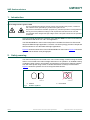
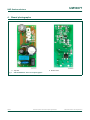
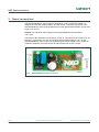
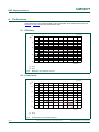
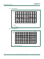
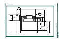
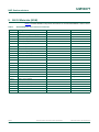
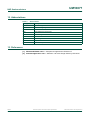
UM10877 SSL5021BDB1211 100 V 9 W buck converter Rev. 1 — 11 March 2015 User manual Document information Info Content Keywords SSL5021BDB1211, SSL5021BTS, non-dimmable, LED driver, buck converter, LED retrofit lamp, LED down light Abstract This user manual describes the operation of the SSL5021BDB1211 100 V 9 W non-dimmable LED driver featuring the SSL5021. The demo board uses a buck topology. It provides a suitable evaluation platform for non-dimmable LED retrofit lamp in low-ripple configurations. UM10877 NXP Semiconductors SSL5021BDB1211 100 V 9 W buck converter Revision history Rev Date Description v.1 20150311 first issue Contact information For more information, please visit: http://www.nxp.com For sales office addresses, please send an email to: [email protected] UM10877 User manual All information provided in this document is subject to legal disclaimers. Rev. 1 — 11 March 2015 © NXP Semiconductors N.V. 2015. All rights reserved. 2 of 16 UM10877 NXP Semiconductors SSL5021BDB1211 100 V 9 W buck converter 1. Introduction WARNING Lethal voltage and fire ignition hazard The non-insulated high voltages that are present when operating this product, constitute a risk of electric shock, personal injury, death and/or ignition of fire. This product is intended for evaluation purposes only. It shall be operated in a designated test area by personnel qualified according to local requirements and labor laws to work with non-insulated mains voltages and high-voltage circuits. This product shall never be operated unattended. This user manual describes the operation of the SSL5021BDB1211 demo board featuring SSL5021BTS LED driver in a 100 V 9 W application. The SSL5021BDB1211 demo board incorporates a suitable form factor for LED retrofit lamp and LED down light applications. The buck converter topology provides a simple and efficient solution for non-dimmable LED light applications. Figure 2 shows the dimensions of the SSL5021BDB1211 demo board. Figure 3 shows the top view and the bottom view photographs. 2. Safety warning The demo board input is connected to the 100 V mains voltage. Avoid touching the board while it is connected to the mains voltage and when it is in operation. An isolated housing is obligatory when used in uncontrolled, non-laboratory environments. Galvanic isolation from the mains phase using a fixed or variable transformer is always recommended. Figure 1 shows the symbols on how to recognize these devices. 019aab174 019aab173 a. Isolated Fig 1. UM10877 User manual b. Not isolated Isolation symbols All information provided in this document is subject to legal disclaimers. Rev. 1 — 11 March 2015 © NXP Semiconductors N.V. 2015. All rights reserved. 3 of 16 UM10877 NXP Semiconductors SSL5021BDB1211 100 V 9 W buck converter 3. Specifications Table 1 lists the specification of the SSL5021BDB1211 demo board. Table 1. SSL5021BDB1211 specifications Symbol Parameter Value Vmains AC mains supply voltage 100 V (AC); 10 % Imains AC mains input power 155 mA (at 100 V (AC)/50 Hz VLED output voltage 40 V ILED output current 209 mA ILED/VLED output voltage rejection 145 A/V efficiency 88 % PF power factor 0.6 Toper operating temperature 40 C to +80 C The SSL5021BDB1211 demo board is designed for functional evaluation. ElectroMagnetic Interference (EMI) and surge test compliances are not intended to perform on this board. Figure 2 shows the dimensions of the demo board. Fig 2. UM10877 User manual SSL5021BDB1211 demo board dimensions All information provided in this document is subject to legal disclaimers. Rev. 1 — 11 March 2015 © NXP Semiconductors N.V. 2015. All rights reserved. 4 of 16 UM10877 NXP Semiconductors SSL5021BDB1211 100 V 9 W buck converter 4. Board photographs a. Top view Fig 3. b. Bottom view SSL5021BDB1211 demo board photographs UM10877 User manual All information provided in this document is subject to legal disclaimers. Rev. 1 — 11 March 2015 © NXP Semiconductors N.V. 2015. All rights reserved. 5 of 16 UM10877 NXP Semiconductors SSL5021BDB1211 100 V 9 W buck converter 5. Board connections The SSL5021BDB1211 demo board is optimized for a 100 V (50/60 Hz) supply. It is designed to work with multiple LEDs or an LED module. The mains connection of the SSL5021BDB1211 demo board is different from other general demo boards. Connect the mains to J1 and J2. Remark: The maximum rated voltage of the SSL5021BDB1211 demo board is 125 V (AC). The anode of the LED load is connected to J3 and J4. The anode is connected to J3, the cathode is connected to J4. Use an LED string with a forward voltage < 50 V on the SSL5021BDB1211 demo board. The expected typical output voltage is 40 V. Under the expected conditions, the output current is 209 mA when set to 100 % output. Fig 4. UM10877 User manual SSL5021BDB1211 board connections All information provided in this document is subject to legal disclaimers. Rev. 1 — 11 March 2015 © NXP Semiconductors N.V. 2015. All rights reserved. 6 of 16 UM10877 NXP Semiconductors SSL5021BDB1211 100 V 9 W buck converter 6. Performance The performance was measured with an 80 V application at an output load of 212 mA. Figure 5 to Figure 8 show the performance data. 6.1 Efficiency DDD Ș 9PDLQV9 (1) 50 Hz (2) 60 Hz Fig 5. Efficiency as a function of Vmains 6.2 Power factor DDD 3) 9PDLQV9 (1) 50 Hz (2) 60 Hz Fig 6. UM10877 User manual Power factor as a function of Vmains All information provided in this document is subject to legal disclaimers. Rev. 1 — 11 March 2015 © NXP Semiconductors N.V. 2015. All rights reserved. 7 of 16 UM10877 NXP Semiconductors SSL5021BDB1211 100 V 9 W buck converter 6.3 Line regulation DDD ,/(' P$ 9PDLQV9 (1) 50 Hz (2) 60 Hz Fig 7. Line regulation 6.4 Load regulation DDD ,/(' P$ Fig 8. UM10877 User manual 9/('9 Load regulation at 50 Hz All information provided in this document is subject to legal disclaimers. Rev. 1 — 11 March 2015 © NXP Semiconductors N.V. 2015. All rights reserved. 8 of 16 UM10877 NXP Semiconductors SSL5021BDB1211 100 V 9 W buck converter 7. Protections The IC incorporates the following protections: • • • • • • UM10877 User manual UnderVoltage LockOut (UVLO) Cycle-by-cycle OverCurrent Protection (OCP) Internal OverTemperature Protection (OTP) Output OverVoltage Protection (OVP) Output Short Protection (OSP) Thermal foldback protection using a Positive Temperature Coefficient (PTC) thermistor All information provided in this document is subject to legal disclaimers. Rev. 1 — 11 March 2015 © NXP Semiconductors N.V. 2015. All rights reserved. 9 of 16 xxxxxxxxxxxxxxxxxxxxx xxxxxxxxxxxxxxxxxxxxxxxxxx xxxxxxx x x x xxxxxxxxxxxxxxxxxxxxxxxxxxxxxx xxxxxxxxxxxxxxxxxxx xx xx xxxxx xxxxxxxxxxxxxxxxxxxxxxxxxxx xxxxxxxxxxxxxxxxxxx xxxxxx xxxxxxxxxxxxxxxxxxxxxxxxxxxxxxxxxxx xxxxxxxxxxxx x x xxxxxxxxxxxxxxxxxxxxx xxxxxxxxxxxxxxxxxxxxxxxxxxxxxx xxxxx xxxxxxxxxxxxxxxxxxxxxxxxxxxxxxxxxxxxxxxxxxxxxxxxxx xxxxxxxx xxxxxxxxxxxxxxxxxxxxxxxxx xxxxxxxxxxxxxxxxxxxx xxx NXP Semiconductors UM10877 User manual 8. Schematic 5 / 5 ' - ) %' 4 5 '(0293 029 5 & *1' &203 & 66/%76 6: 9&& ,616 5 & 5 5 & 5 / 1 57 - /(' 5 ' & 5 5 5 - /(' DDD Fig 9. SSL5021BDB1211 demo board schematic diagram UM10877 10 of 16 © NXP Semiconductors N.V. 2015. All rights reserved. 5 SSL5021BDB1211 100 V 9 W buck converter Rev. 1 — 11 March 2015 All information provided in this document is subject to legal disclaimers. 8 / - 5 & UM10877 NXP Semiconductors SSL5021BDB1211 100 V 9 W buck converter 9. Bill Of Materials (BOM) Table 2 provides detailed component information for the SSL5021BDB1211 demo board. Table 2. SSL5021BDB1211 demo board bill of materials Reference Description and values Part number Manufacturer BD1 bridge diode; 600 V; 0.5 A; MBS-1 MB6S Fairchild C1 capacitor; 0.047 F; 125 V (AC) B32620A3473J EPCOS C2 capacitor; 10 F; 200 V 200BXC10U10X16 Rubycon C3 capacitor; 220 pF; 50 V; 1608 GRM1885C2A221JA01D Murata C4 capacitor; 1000 pF; 1608 GRM1885C1H102JA01J Murata C5 capacitor; 1 F; 1608 GRM188R71E105KA12D Murata C6 capacitor; 1 F; 100 V; 3216 GRM31CR72A105KA01K Murata D1 diode; 600 V; 1 A; DO-41 STTH2R06RL ST Micro D2 diode; Schottky; 30 V; 220 mA; SOD323F BAT54J NXP Semiconductors F1 fuse; 1 A; 125 V (AC) RST1 Bel Fuse L1; L2 inductor; 680 H; 7447462681 Würth Elektronik MOV1 movistor; 240 V S07K150 EPCOS Q1 MOSFET; 600 V; 2 A; IPAK FQU2N60CTU Fairchild R1 resistor; 4.7 ; 1 W ERX-1SJ4R7 Panasonic R2 resistor; 2.2 k; 3216 ERJ-8ENF2201V Panasonic R3; R4 resistor; 200 k; 2012 ERJ-6ENF2003V Panasonic R5 resistor; 100 ; 1608 ERJ-3EKF1000V Panasonic R6 resistor; 22 k; 2012 ERJ-6ENF2202V Panasonic R7 resistor; 3.3 ; 1 %; 3216 CRCW12063R30FKEA Vishay R8 resistor; 4.7 ; 1 %; 3216 CRCW12064R70FKEA Vishay R9; R11 resistor; not mounted - - R10 resistor; 5.1 k; 1 %; 1608 ERJ-3EKF5101V Panasonic R12; R13 resistor; 100 k; 1 %; 2012 ERJ-6ENF1003V Panasonic R14 resistor; 56 k; 2012 ERJ-6ENF5602V Panasonic RT1 thermistor; 1608 PRF18BC471QB5RB Panasonic U1 LED driver; TSOP6 SSL5021BTS NXP Semiconductors UM10877 User manual All information provided in this document is subject to legal disclaimers. Rev. 1 — 11 March 2015 © NXP Semiconductors N.V. 2015. All rights reserved. 11 of 16 UM10877 NXP Semiconductors SSL5021BDB1211 100 V 9 W buck converter 10. Tuning options 10.1 Output current The SSL5021BDB1211 demo board is suitable for 60 W equivalent LED retrofit lamp designs when 40 V LED strings are connected to J3 and J4. To tune an output current for different output voltage settings or other output settings, sense resistors R7 and R8 can 0.41 be adjusted. I LED AV = ------------------------------------ calculates the estimated ILED(AV) (where 0.06 is R sense + 0.06 bond wire resistance of ISNS pin). The L2 saturation current is 600 mA. If 250 mA or a higher output current is required, choose an appropriate inductor. 10.2 Wall switch with pilot lamp To deliver a wall switch with pilot lamp compatibility, resistor R6 is set to 22 k. It creates a small current path while Q1 is in off-state. Many wall switches with pilot lamps feed a current to the lamp while in off-state because of an impedance of 1 M or higher. A small current flowing through the switch is bypassed. The VCC voltage of the SSL5021BTS does not reach the start-up level while the wall switch with pilot lamp is in off-state. To retain the off-state, specific wall switches require a higher bypass current. The SSL5021BDB1211 demo board is designed for most popular wall switches. If compatibility with specific switches is required, decrease the value of resistor R6. The result of decreasing the resistor value is some loss on the resistor. Resistor R9 is an alternative implementation for wall switches with pilot lamp compatibility. UM10877 User manual All information provided in this document is subject to legal disclaimers. Rev. 1 — 11 March 2015 © NXP Semiconductors N.V. 2015. All rights reserved. 12 of 16 UM10877 NXP Semiconductors SSL5021BDB1211 100 V 9 W buck converter 11. Board layout Figure 10 and Figure 11 show the layout of both layers. a. Top view b. Bottom view Fig 10. SSL5021BDB1211 demo board layout (silk) a. Pattern b. Drill Fig 11. SSL5021BDB1211 demo board layout (pattern and drill) UM10877 User manual All information provided in this document is subject to legal disclaimers. Rev. 1 — 11 March 2015 © NXP Semiconductors N.V. 2015. All rights reserved. 13 of 16 UM10877 NXP Semiconductors SSL5021BDB1211 100 V 9 W buck converter 12. Abbreviations Table 3. Abbreviations Acronym Description LED Light-Emitting Diode SSL Solid-State Lighting PF Power Factor EMI ElectroMagnetic Interference UVLO UnderVoltage LockOut OCP OverCurrent Protection OVP OverVoltage Protection OSP Output Short Protection PTC Positive Temperature Coefficient 13. References UM10877 User manual [1] SSL5021BTS data sheet — Compact low-ripple buck LED driver IC [2] AN11532 application note — SSL50x1 4 W to 25 W high-efficiency LED driver All information provided in this document is subject to legal disclaimers. Rev. 1 — 11 March 2015 © NXP Semiconductors N.V. 2015. All rights reserved. 14 of 16 UM10877 NXP Semiconductors SSL5021BDB1211 100 V 9 W buck converter 14. Legal information 14.1 Definitions Draft — The document is a draft version only. The content is still under internal review and subject to formal approval, which may result in modifications or additions. NXP Semiconductors does not give any representations or warranties as to the accuracy or completeness of information included herein and shall have no liability for the consequences of use of such information. NXP Semiconductors does not accept any liability related to any default, damage, costs or problem which is based on any weakness or default in the customer’s applications or products, or the application or use by customer’s third party customer(s). Customer is responsible for doing all necessary testing for the customer’s applications and products using NXP Semiconductors products in order to avoid a default of the applications and the products or of the application or use by customer’s third party customer(s). NXP does not accept any liability in this respect. Export control — This document as well as the item(s) described herein may be subject to export control regulations. Export might require a prior authorization from competent authorities. 14.2 Disclaimers Limited warranty and liability — Information in this document is believed to be accurate and reliable. However, NXP Semiconductors does not give any representations or warranties, expressed or implied, as to the accuracy or completeness of such information and shall have no liability for the consequences of use of such information. NXP Semiconductors takes no responsibility for the content in this document if provided by an information source outside of NXP Semiconductors. In no event shall NXP Semiconductors be liable for any indirect, incidental, punitive, special or consequential damages (including - without limitation - lost profits, lost savings, business interruption, costs related to the removal or replacement of any products or rework charges) whether or not such damages are based on tort (including negligence), warranty, breach of contract or any other legal theory. Notwithstanding any damages that customer might incur for any reason whatsoever, NXP Semiconductors’ aggregate and cumulative liability towards customer for the products described herein shall be limited in accordance with the Terms and conditions of commercial sale of NXP Semiconductors. Right to make changes — NXP Semiconductors reserves the right to make changes to information published in this document, including without limitation specifications and product descriptions, at any time and without notice. This document supersedes and replaces all information supplied prior to the publication hereof. Suitability for use — NXP Semiconductors products are not designed, authorized or warranted to be suitable for use in life support, life-critical or safety-critical systems or equipment, nor in applications where failure or malfunction of an NXP Semiconductors product can reasonably be expected to result in personal injury, death or severe property or environmental damage. NXP Semiconductors and its suppliers accept no liability for inclusion and/or use of NXP Semiconductors products in such equipment or applications and therefore such inclusion and/or use is at the customer’s own risk. Applications — Applications that are described herein for any of these products are for illustrative purposes only. NXP Semiconductors makes no representation or warranty that such applications will be suitable for the specified use without further testing or modification. Customers are responsible for the design and operation of their applications and products using NXP Semiconductors products, and NXP Semiconductors accepts no liability for any assistance with applications or customer product design. It is customer’s sole responsibility to determine whether the NXP Semiconductors product is suitable and fit for the customer’s applications and products planned, as well as for the planned application and use of customer’s third party customer(s). Customers should provide appropriate design and operating safeguards to minimize the risks associated with their applications and products. Evaluation products — This product is provided on an “as is” and “with all faults” basis for evaluation purposes only. NXP Semiconductors, its affiliates and their suppliers expressly disclaim all warranties, whether express, implied or statutory, including but not limited to the implied warranties of non-infringement, merchantability and fitness for a particular purpose. The entire risk as to the quality, or arising out of the use or performance, of this product remains with customer. In no event shall NXP Semiconductors, its affiliates or their suppliers be liable to customer for any special, indirect, consequential, punitive or incidental damages (including without limitation damages for loss of business, business interruption, loss of use, loss of data or information, and the like) arising out the use of or inability to use the product, whether or not based on tort (including negligence), strict liability, breach of contract, breach of warranty or any other theory, even if advised of the possibility of such damages. Notwithstanding any damages that customer might incur for any reason whatsoever (including without limitation, all damages referenced above and all direct or general damages), the entire liability of NXP Semiconductors, its affiliates and their suppliers and customer’s exclusive remedy for all of the foregoing shall be limited to actual damages incurred by customer based on reasonable reliance up to the greater of the amount actually paid by customer for the product or five dollars (US$5.00). The foregoing limitations, exclusions and disclaimers shall apply to the maximum extent permitted by applicable law, even if any remedy fails of its essential purpose. Safety of high-voltage evaluation products — The non-insulated high voltages that are present when operating this product, constitute a risk of electric shock, personal injury, death and/or ignition of fire. This product is intended for evaluation purposes only. It shall be operated in a designated test area by personnel that is qualified according to local requirements and labor laws to work with non-insulated mains voltages and high-voltage circuits. The product does not comply with IEC 60950 based national or regional safety standards. NXP Semiconductors does not accept any liability for damages incurred due to inappropriate use of this product or related to non-insulated high voltages. Any use of this product is at customer’s own risk and liability. The customer shall fully indemnify and hold harmless NXP Semiconductors from any liability, damages and claims resulting from the use of the product. Translations — A non-English (translated) version of a document is for reference only. The English version shall prevail in case of any discrepancy between the translated and English versions. 14.3 Trademarks Notice: All referenced brands, product names, service names and trademarks are the property of their respective owners. GreenChip — is a trademark of NXP Semiconductors N.V. UM10877 User manual All information provided in this document is subject to legal disclaimers. Rev. 1 — 11 March 2015 © NXP Semiconductors N.V. 2015. All rights reserved. 15 of 16 UM10877 NXP Semiconductors SSL5021BDB1211 100 V 9 W buck converter 15. Contents 1 2 3 4 5 6 6.1 6.2 6.3 6.4 7 8 9 10 10.1 10.2 11 12 13 14 14.1 14.2 14.3 15 Introduction . . . . . . . . . . . . . . . . . . . . . . . . . . . . 3 Safety warning . . . . . . . . . . . . . . . . . . . . . . . . . . 3 Specifications. . . . . . . . . . . . . . . . . . . . . . . . . . . 4 Board photographs . . . . . . . . . . . . . . . . . . . . . . 5 Board connections . . . . . . . . . . . . . . . . . . . . . . 6 Performance . . . . . . . . . . . . . . . . . . . . . . . . . . . . 7 Efficiency . . . . . . . . . . . . . . . . . . . . . . . . . . . . . 7 Power factor . . . . . . . . . . . . . . . . . . . . . . . . . . . 7 Line regulation . . . . . . . . . . . . . . . . . . . . . . . . . 8 Load regulation . . . . . . . . . . . . . . . . . . . . . . . . . 8 Protections . . . . . . . . . . . . . . . . . . . . . . . . . . . . . 9 Schematic . . . . . . . . . . . . . . . . . . . . . . . . . . . . . 10 Bill Of Materials (BOM) . . . . . . . . . . . . . . . . . . 11 Tuning options . . . . . . . . . . . . . . . . . . . . . . . . . 12 Output current. . . . . . . . . . . . . . . . . . . . . . . . . 12 Wall switch with pilot lamp . . . . . . . . . . . . . . . 12 Board layout . . . . . . . . . . . . . . . . . . . . . . . . . . . 13 Abbreviations . . . . . . . . . . . . . . . . . . . . . . . . . . 14 References . . . . . . . . . . . . . . . . . . . . . . . . . . . . 14 Legal information. . . . . . . . . . . . . . . . . . . . . . . 15 Definitions . . . . . . . . . . . . . . . . . . . . . . . . . . . . 15 Disclaimers . . . . . . . . . . . . . . . . . . . . . . . . . . . 15 Trademarks. . . . . . . . . . . . . . . . . . . . . . . . . . . 15 Contents . . . . . . . . . . . . . . . . . . . . . . . . . . . . . . 16 Please be aware that important notices concerning this document and the product(s) described herein, have been included in section ‘Legal information’. © NXP Semiconductors N.V. 2015. All rights reserved. For more information, please visit: http://www.nxp.com For sales office addresses, please send an email to: [email protected] Date of release: 11 March 2015 Document identifier: UM10877