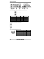
1
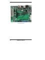
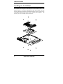
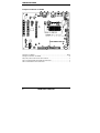
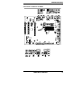
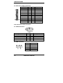
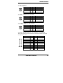
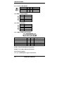
IP400
ETX Baseboard
USER’S MANUAL
Version 1.0
Acknowledgments
Award is a registered trademark of Award Software International,
Inc.
PS/2 is a trademark of International Business Machines
Corporation.
Intel and Pentium M are registered trademarks of Intel
Corporation.
Microsoft Windows is a registered trademark of Microsoft
Corporation.
Winbond is a registered trademark of Winbond Electronics
Corporation.
All other product names or trademarks are properties of their
respective owners.
ii
IP400 User’s Manual
Table of Contents
Introduction .......................................................1
IP400 Specifications............................................................ 1
Board Dimensions ............................................................... 2
Installations .......................................................3
Installing the CPU Module.................................................. 4
Setting the Jumpers ............................................................. 5
Connectors on IP400 ........................................................... 8
IP400 User’s Manual
iii
The IP400 Baseboard
iv
IP400 User’s Manual
INTRODUCTION
Introduction
IP400 Specifications
[
Product Name
IP400 (for COM ETX module)
Form Factor
Flex ATX for COM ETX CPU module
Battery
Lithium Battery for real time clock
Audio
Derived from COMETX Module AC97 Codec ALC655 w/ 6
channels (Line-out, Line-in, Mic.) + NS LM4940 8ohm 2W stereo
audio power amplifier
USB
Derived from COMETX Module, pin header (8 ports)
IDE
Derived from COMETX Module, one channel Compact Flash Type
II and DOM
VGA
Derived from COMETX Module, DB15 connector
LVDS
Derived from COMETX Module, DF13 connector x 2
TV-Out
Derived from COMETX Module, composite connector
LAN
Derived from COMETX Module, 10/100BT LAN1
Marvell 88E8053 PCI-e Gigabit LAN controller x1 for LAN2
Super IO
Winbond LPC I/F SIO W83627EHF: Parallel x1, COM1, COM2
(RS232), Slim FDC 1.44MB, IrDA x1, PS/2 KB/Mouse & hardware
monitor (3 thermal inputs, 4 voltage monitor inputs, VID0-4, 3 fan
headers)
2nd Super IO (option)
Fintek F81216D for COM3, 4 (RS-232)
Digital I/O
Supports 4 in and 4 out w/ pin header
Watch-Dog Timer
Yes (256 segments: 0, 1, 2,..., 255 sec/min)
Edge Connector
(With the same I/O
shield w/ IP400)
DB15 + DB9 stack connector x1for VGA & COM1
Dual USB stack connector for USB1, 2
Dual RJ45 stack connector x1 for LAN1, 2
PS/2 DIN connector x1
RCA connector x3 for Audio (Line-out, Line-in & Mic)
SPDIF connector x1
S-Video connector x1
RCA connector x1 for TV-Out
Onboard Connector /
Header
44-pin header x1 for HDDs & DOM
DF13 x2 for LVDS
SATA connector x2 for two SATA HDDs
5x2 pins header x3 for COM2~4
4x2 pins header x3 for USB3~8
34-pin box-header x 1 for Floppy
26-pin box-header x 1 for Printer
PCI-e 16-lane slot x1
PCI-e 1-lane slot x1
PCI (32-bit) slot x2
Expansion Slots
PCB Layer
4 layers
Board Size
7.5” x 9”
IP400 User’s Manual
1
INTRODUCTION
Board Dimensions
2
IP400 User’s Manual
INSTALLATIONS
Installations
This section provides information on how to use the jumpers and
connectors on the IP400 in order to set up a workable system. The topics
covered are:
Installing the CPU Module.................................................. 4
Setting the Jumpers ............................................................. 5
Connectors on IP400 ........................................................... 8
IP400 User’s Manual
3
INSTALLATIONS
Installing the CPU Module
The IP400 board supports COM Express CPU module such as the
ET810. Below is a picture showing how the CPU module and the
heatsink should be installed on the IP400 baseboard. There are five holes
on the IP400 that can be used to screw the three parts together – the
heatsink, the CPU module and the baseboard.
4
IP400 User’s Manual
INSTALLATIONS
Setting the Jumpers
Jumpers are used on IP400 to select various settings and features
according to your needs and applications. Contact your supplier if you
have doubts about the best configuration for your needs. The following
lists the connectors on IP400 and their respective functions.
Jumper Locations on IP400 ............................................................ 6
JP2, JP3, JP4: ATX Power On Control .......................................... 7
JP5: CompactFlash Slave/Master Selection ................................... 7
JP6: LCD Panel Power Selection ................................................... 7
[
IP400 User’s Manual
5
INSTALLATIONS
Jumper Locations on IP400
Jumpers on IP400 ............................................................................ Page
Jumper Locations on IP400 ................................................................... 6
JP2, JP3, JP4: ATX Power On Control ................................................. 7
JP5: CompactFlash Slave/Master Selection........................................... 7
JP6: LCD Panel Power Selection .......................................................... 7
[
6
IP400 User’s Manual
INSTALLATIONS
JP2, JP3, JP4: ATX Power On Control
JP2, JP3
JP4
ATX Power On Control
With LPC I/O
With COM Express’ Southbridge
JP5: CompactFlash Slave/Master Selection
JP5
CF Setting
Master
Slave
[
JP6: LCD Panel Power Selection
JP6
LCD Panel Power
3.3V
5V
IP400 User’s Manual
7
INSTALLATIONS
Connectors on IP400
The connectors on IP400 allows you to connect external devices such as
keyboard, floppy disk drives, hard disk drives, printers, etc. The
following table lists the connectors on IP400 and their respective
functions.
Connector Locations on IP400 ....................................................... 9
CN2: PS/2 Keyboard and PS/2 Mouse Connectors ...................... 10
J8: S-Video and RCA Connectors ................................................ 10
CN3: COM1 and VGA Connector ............................................... 10
CN6: 10/100 RJ-45 and USB1/2 Ports ......................................... 11
J15: SPDIF Out Connector ........................................................... 11
CN7: Gigabit RJ-45 and USB3/4 Ports ........................................ 11
CN8: Audio Connector ................................................................. 11
CN1: Parallel Port Connector ....................................................... 11
FDD1: Floppy Drive Connector ................................................... 12
IDE1: IDE Connector ................................................................... 12
FAN1: CPU Fan Power Connector............................................... 13
FAN2: System Fan Power Connector........................................... 13
J1: Wake On LAN Connector....................................................... 13
J2: Digital I/O ............................................................................... 13
J3: ATX_12V Connector.............................................................. 13
J4: ATX Power Supply Connector ............................................... 14
CN4, CN5: Serial ATA Connectors ............................................. 14
J5: COM2 Serial Port.................................................................... 14
J6: IrDA Connector ...................................................................... 14
J7: TV out (DF11) ........................................................................ 15
J9: USB7, USB8 Port Pin Header................................................. 15
J12: USB5, USB6 Port Pin Header............................................... 15
J13, J14: LVDS Connectors (1st channel, 2nd channel) .............. 15
J17: Line out / Mic Header ........................................................... 16
J18: AMP Line Out Header .......................................................... 16
J19: CD-In Connector................................................................... 16
J21: COM3, COM4 20-pin Header .............................................. 16
PCIE_1: 16-line PCI-Express Connector ..................................... 16
PCIE_2: 1-line PCI –Express Connector...................................... 16
PCI1, PCI2: PCI Slots................................................................... 16
J10, J11: COM Express Type 2 Connectors ................................. 16
8
IP400 User’s Manual
INSTALLATIONS
Connector Locations on IP400
IP400 User’s Manual
9
INSTALLATIONS
CN2: PS/2 Keyboard and PS/2 Mouse Connectors
PS/2 Mouse
PS/2 Keyboard
Signal Name
Keyboard data
N.C.
GND
5V
Keyboard clock
N.C.
Keyboard
1
2
3
4
5
6
Mouse
1
2
3
4
5
6
Signal Name
Mouse data
N.C.
GND
5V
Mouse clock
N.C.
J8: S-Video and RCA Connectors
CN3: COM1 and VGA Connector
Signal Name Pin #
DCD
1
RXD
2
TXD
3
DTR
4
COM1
GND
5
[
10
IP400 User’s Manual
Pin # Signal Name
6
DSR
7
RTS
8
CTS
9
RI
10
Not Used
INSTALLATIONS
[[[[
VGA
Signal Name
Red
Blue
GND
GND
N.C.
N.C.
HSYNC
NC
Pin #
1
3
5
7
9
11
13
15
Pin # Signal Name
2
Green
4
N.C.
6
GND
8
GND
10
GND
12
N.C.
14
VSYNC
CN6: 10/100 RJ-45 and USB1/2 Ports
J15: SPDIF Out Connector
CN7: Gigabit RJ-45 and USB3/4 Ports
CN8: Audio Connector
CN1: Parallel Port Connector
CN1
Signal Name
Line printer strobe
PD0, parallel data 0
PD1, parallel data 1
PD2, parallel data 2
PD3, parallel data 3
PD4, parallel data 4
PD5, parallel data 5
PD6, parallel data 6
PD7, parallel data 7
ACK, acknowledge
Busy
Paper empty
Select
Pin #
1
2
3
4
5
6
7
8
9
10
11
12
13
IP400 User’s Manual
Pin #
14
15
16
17
18
19
20
21
22
23
24
25
N/A
Signal Name
AutoFeed
Error
Initialize
Select
Ground
Ground
Ground
Ground
Ground
Ground
Ground
Ground
N/A
11
INSTALLATIONS
FDD1: Floppy Drive Connector
FDD1is a slim 26-pin connector and will support up to 2.88MB FDD.
Signal Name
Pin #
Pin #
Signal Name
VCC
VCC
VCC
NC
NC
DINST
NC
GND
GND
GND
NC
GND
GND
1
3
5
7
9
11
13
15
17
19
21
23
25
2
4
6
8
10
12
14
16
18
20
22
24
26
INDEX
DRV_SEL
DSK_CH
NC
MOTOR
DIR
STEP
WDATA
WGATE
TRACK
WPROT
RDATA
SIDE
IDE1: IDE Connector
Signal Name
Reset IDE
Host data 7
Host data 6
Host data 5
Host data 4
Host data 3
Host data 2
Host data 1
Host data 0
Ground
DRQ0
Host IOW
Host IOR
IOCHRDY
DACK0
IRQ14
Address 1
Address 0
Chip select 0
Activity
12
Pin #
1
3
5
7
9
11
13
15
17
19
21
23
25
27
29
31
33
35
37
39
Pin #
2
4
6
8
10
12
14
16
18
20
22
24
26
28
30
32
34
36
38
40
IP400 User’s Manual
Signal Name
Ground
Host data 8
Host data 9
Host data 10
Host data 11
Host data 12
Host data 13
Host data 14
Host data 15
Protect pin
Ground
Ground
Ground
Host ALE
Ground
No connect
No connect
Address 2
Chip select 1
Ground
INSTALLATIONS
FAN1: CPU Fan Power Connector
FAN1 is a 3-pin header for the CPU fan. The fan must be a 12V fan.
Pin #
1
2
3
Signal Name
Ground
+12V
Rotation detection
FAN2: System Fan Power Connector
Pin #
1
2
3
Signal Name
Ground
+12V
Rotation detection
J1: Wake On LAN Connector
J1 is a 3-pin header for the Wake On LAN function which will function
properly only with an ATX power supply with 5VSB that has 200mA.
Pin #
1
2
3
J2: Digital I/O
Signal Name
GND
OUT3
OUT2
IN3
IN2
Pin
1
3
5
7
9
Signal Name
+5VSB
Ground
-PME
Pin
2
4
6
8
10
Signal Name
VCC
OUT1
OUT0
IN1
IN0
J3: ATX_12V Connector
J3 can be used in situations where the 12V current from the ATX power
is insufficient to supply needed current.
Pin #
1
2
3
4
Signal Name
Ground
Ground
+12V
+12V
IP400 User’s Manual
13
INSTALLATIONS
J4: ATX Power Supply Connector
Signal Name Pin #
3.3V
13
-12V
14
Ground
15
PS-ON
16
Ground
17
Ground
18
Ground
19
-5V
20
+5V
21
+5V
22
+5V
23
Ground
24
Pin #
1
2
3
4
5
6
7
8
9
10
11
12
Signal Name
3.3V
3.3V
Ground
+5V
Ground
+5V
Ground
Power good
5VSB
+12V
+12V
+3.3V
CN4, CN5: Serial ATA Connectors
J5: COM2 Serial Port
COM2
Signal Name
DCD, Data carrier detect
RXD, Receive data
TXD, Transmit data
DTR, Data terminal ready
GND, ground
Pin #
1
2
3
4
5
Pin #
6
7
8
9
10
Signal Name
DSR, Data set ready
RTS, Request to send
CTS, Clear to send
RI, Ring indicator
Not Used
J6: IrDA Connector
Pin #
1
2
3
4
5
14
Signal Name
+5V
No connect
Ir RX
Ground
Ir TX
IP400 User’s Manual
INSTALLATIONS
J7: TV out (DF11)
Signal Name
NC
Y
C/Pr
CVBS/Pb
Pin
1
3
5
7
Pin
2
4
6
8
Signal Name
NC
Ground
Ground
Ground
J9: USB7, USB8 Port Pin Header
Signal Name Pin Pin
Vcc
1
5
D2
6
D+
3
7
Ground
4
8
Signal Name
Ground
D+
DVcc
J12: USB5, USB6 Port Pin Header
Signal Name Pin Pin
Vcc
1
5
D2
6
D+
3
7
Ground
4
8
Signal Name
Ground
D+
DVcc
J13, J14: LVDS Connectors (1st channel, 2nd channel)
The LVDS connectors on board consist of the first channel (J13) and
second channel (J14).
Signal Name
TX0Ground
TX15V/3.3V
TX3TX2Ground
TXC5V/3.3V
+12V
Pin #
2
4
6
8
10
12
14
16
18
20
Pin #
1
3
5
7
9
11
13
15
17
19
IP400 User’s Manual
Signal Name
TX0+
Ground
TX1+
Ground
TX3+
TX2+
Ground
TXC+
ENABKL
+12V
15
INSTALLATIONS
J17: Line out / Mic Header
Signal Name Pin
R out
1
GND
3
Mic1
7
Pin
2
4
8
Signal Name
L out
GND
Mic2
J18: AMP Line Out Header
Pin #
1
2
3
4
Signal Name
L out
Ground
Ground
R out
J19: CD-In Connector
Pin #
1
2
3
4
Signal Name
CD L
Ground
Ground
CD R
J21: COM3, COM4 20-pin Header
Signal Name
DCD, Data carrier detect
RXD, Receive data
TXD, Transmit data
DTR, Data terminal ready
GND, Ground
Pin #
1
3
5
7
9
Pin #
2
4
6
8
10
Signal Name
DSR, Data set ready
RTS, Request to send
CTS, Clear to send
RI, Ring indicator
Not used
PCIE_1: 16-line PCI-Express Connector
PCIE_2: 1-line PCI –Express Connector
PCI1, PCI2: PCI Slots
J10, J11: COM Express Type 2 Connectors
16
IP400 User’s Manual
APPENDIX
IP400 User’s Manual
17