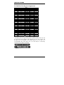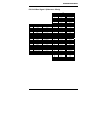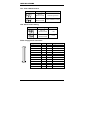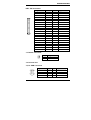
1
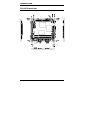
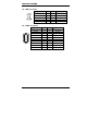
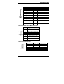
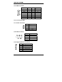
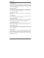
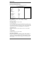
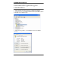
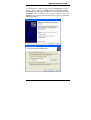
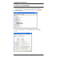
IB704
AMD Geode LX800
PC/104-Plus CPU Module
USER’S MANUAL
Version 1.0
Acknowledgments
Award is a registered trademark of Award Software International,
Inc.
PS/2 are trademarks of International Business Machines
Corporation.
Crusoe and LongRun are registered trademarks of Transmeta
Corporation.
Microsoft Windows is a registered trademark of Microsoft
Corporation.
Winbond is a registered trademark of Winbond Electronics
Corporation.
All other product names or trademarks are properties of their
respective owners.
ii
IB104+ User’s Manual
Table of Contents
Introduction .......................................................1
Product Description............................................................. 1
Checklist.............................................................................. 2
Specifications ...................................................................... 3
Board Dimensions ............................................................... 4
Installations .......................................................5
Installing the Memory (SODIMM) ..................................... 6
Jumpers and Connector on IB704 ....................................... 7
BIOS Setup .......................................................17
Drivers Installation ......................................35
Entertainment Encryption/Decryption Controller Driver.. 36
VGA Drivers Installation .................................................. 38
Appendix ...........................................................42
A. I/O Port Address Map................................................... 42
B. Interrupt Request Lines (IRQ) ...................................... 43
C. Watchdog Timer Configuration.................................... 44
IB104+ User’s Manual
iii
This page is intentionally left blank.
iv
IB704 User’s Manual
INTRODUCTION
Introduction
Product Description
The IB704 PC/104 Plus module features the AMD Geode CS5536
companion device that is optimized to work with the AMD Geode LX
[email protected] processor. With a compact 90mm x 96mm footprint standard,
the IB704 is suited for space-constraint applications in factory
automation, military, security, transportation and POS. The board does
not require a fan and features extended temperature operation that
enables it to perform in harsh environment..
The IB704 delivers the highest power/performance ratio available in the
industry and comes with advanced graphics, connectivity and expansion
features. On board is one SO-DIMM socket supporting up to 1GB of DDR
SDRAM. The integrated VGA controller supports for CRT and LVDS LCD
displays. Connectivity interfaces include the PC/104+ connector and a
10/100 BaseT Ethernet, four USB 2.0 and two serial ports.
FEATURES
•
Embedded AMD Geode LX700 (433MHz) / LX800 (500MHz)
•
DDR SO-DIMM x 1, Max. 1GB
•
Realtek RTL8100C 10/100 BaseT Ethernet
•
Integrated LX800/LX700 2D VGA controller, supports CRT and
LVDS interfaces
•
4 x USB 2.0, 2 x COM, Watchdog timer
•
PC/104+ connector (PCI+ISA)
•
Extended Temperature (-20C ~ 80C)
Remarks: In installing the PC/104 Plus CPU board into a chassis, it is
recommended that the CPU board be placed on the topmost level of the
PC/104 board layers. The chassis environment should be designed in
such a way that there is good airflow to ventilate the system.
IB704 User’s Manual
1
INTRODUCTION
Checklist
Your IB704 package should include the items listed below. Damaged or
missing items should be reported to your supplier.
• The IB704 CPU Module
• This User’s Manual
• One Driver CD
• Optional cable kit (IDE7, IDE6, PK3-2, PS2G, VGA8, RJ45A2,
USB2-2, PK1-12, FF2)
2
IB704 User’s Manual
INTRODUCTION
Specifications
Form Factor
CPU Type
CPU Operating
Frequency
Green / APM
BIOS
Chipset
Memory
Graphics
LAN Controller
IDE
USB
LPC I/O
RTC/CMOS
PCI Arbiter
PCI to ISA Bridge
Watchdog Timer
On Board header
Operating
Temperature
Board Size
PC/104+
AMD Geode LX processor
LX800 @500MHz (IB704F)
LX700 @433MHz (IB704)
APM1.2
Award BIOS (4MB FWH)
AMD CS5536 I/O companion multi-function south
bridge
One DDR SODIMM socket, Max. Up to 1GB
LX800/LX700 built-in high performance 2D
graphic controller, supports LVDS LCD & CRT
display
Realtek RTL8100C-LF 10/100Mbps
CS5536 built-in one channel UDMA100 IDE
CS5536 built-in USB2.0 controller, support 4
ports
Winbond W83627HG: KB/Mouse controller,
Parallel, IrDA, Floppy, COM1, COM2 (RS232) &
Hardware monitor (3 thermal inputs, 4 voltage
monitor inputs)
Geode CS5536 built-in w/ on board Lithium
battery
ITE IT8209R PCI arbiter/clock buffer chip, extend
PCI devices (master) from 1 to 3
ITE IT8888G
Yes (256 segments, 0, 1, 2…255. sec/min)
PC/104+ (PCI + ISA) connector set x1
2x8 pin-header x1 for VGA
2x13 pin-header x1 for parallel port
2x5 pin-header x2 for COM1, 2
2x4 pin-header x2 for USB
2x22 box-header x1 for IDE
2x5 pin-header x1 for LAN
DF13-20 connector x1 for LVDS
6-pin pin-header x1 for PS/2 KB&MS
5-pin pin-header x1 for IrDA
4-pin FDD power connector x1 for system power
input.
-20°C ~ 70°C (68°F ~158°F)
96mm x 90mm
IB704 User’s Manual
3
INTRODUCTION
Board Dimensions
4
IB704 User’s Manual
INSTALLATIONS
Installations
This section provides information on how to use the jumpers and
connectors on the IB704 in order to set up a workable system. The topics
covered are:
Installing the Memory (SODIMM).............................................. 6
Jumpers and Connector on IB704................................................ 7
IB704 User’s Manual
5
INSTALLATIONS
Installing the Memory (SODIMM)
The IB704 has a 144-pin SODIMM socket. The SODIMM socket
supports a maximum total memory of 1GB.
Installing and Removing DIMMs
To install the SODIMM, locate the memory slot on the CPU module and
perform the following steps:
1. Hold the SODIMM so that the two keys of the DIMM align with those
on the memory slot.
2. Gently push the SODIMM in an upright position until the clips of the
slot close to hold the DIMM in place when the SODIMM touches the
bottom of the slot.
3. To remove the SODIMM, press the clips with both hands.
Top View of SODIMM Socket
6
IB704 User’s Manual
INSTALLATIONS
Jumpers and Connector on IB704
Jumpers are used on the IB704 to select various settings and features
according to your needs and applications. Contact your supplier if you
have doubts about the best configuration for your needs. The following
lists the connectors on IB704 and their respective functions.
Jumper and Connector Locations on IB704 .......................................... 8
J15 & J16: PC/104 Connector ............................................................... 9
PC/104-Plus Bus Signal Assignments ................................................. 10
PC/104 Bus Signal (Reference Only).................................................. 11
JP1: Clear CMOS Content................................................................... 12
JP2: Panel Power Setting..................................................................... 12
FDD1: Floppy Drive Connector .......................................................... 12
IDE1: IDE Connector .......................................................................... 13
J1: Buzzer Connector .......................................................................... 13
J3: PC/104+ PCI .................................................................................. 13
J4, J5: USB Connector ........................................................................ 13
J6: LAN Connector.............................................................................. 14
J8: LVDS Connector ........................................................................... 14
J9: Parallel Port Connector .................................................................. 15
J11, J13: COM1 and COM2 Connectors............................................. 15
J12: Front I/O Connector..................................................................... 15
J14: VGA Connector ........................................................................... 16
J15, J16: PC/104+ ISA ........................................................................ 16
J17: Power Connector.......................................................................... 16
J18: IrDA Connector ........................................................................... 16
J19: Keyboard/Mouse Connector ........................................................ 16
IB704 User’s Manual
7
INSTALLATIONS
Jumper and Connector Locations on IB704
Jumper and Connectors on IB704 ............................................................................Page
J15 & J16: PC/104 Connector ........................................................................................9
PC/104-Plus Bus Signal Assignments..........................................................................10
PC/104 Bus Signal (Reference Only)...........................................................................11
JP1: Clear CMOS Content............................................................................................12
JP2: Panel Power Setting ..............................................................................................12
FDD1: Floppy Drive Connector ...................................................................................12
IDE1: IDE Connector ...................................................................................................13
J1: Buzzer Connector....................................................................................................13
J3: PC/104+ PCI ...........................................................................................................13
J4, J5: USB Connector..................................................................................................13
J6: LAN Connector.......................................................................................................14
J8: LVDS Connector.....................................................................................................14
J9: Parallel Port Connector ...........................................................................................15
J11, J13: COM1 and COM2 Connectors......................................................................15
J12: Front I/O Connector..............................................................................................15
J14: VGA Connector ....................................................................................................16
J15, J16: PC/104+ ISA .................................................................................................16
J17: Power Connector...................................................................................................16
J18: IrDA Connector.....................................................................................................16
J19: Keyboard/Mouse Connector .................................................................................16
8
IB704 User’s Manual
INSTALLATIONS
J15 & J16: PC/104 Connector
J15 and J16 are dual-in-line pin headers that support PC-104 modules.
J15 consists of 64 pins and J16 has 40 pins.
Pin
A1
A2
A3
A4
A5
A6
A7
A8
A9
A10
A11
A12
A13
A14
ZA15
A16
A17
A18
A19
A20
A21
A22
A23
A24
A25
A26
A27
A28
A29
A30
A31
A32
J15
Signal Name Pin
IOCHK
B1
D7
B2
D6
B3
D5
B4
D4
B5
D3
B6
D2
B7
D1
B8
D0
B9
IOCHRDY
B10
AEN
B11
A19
B12
A18
B13
A17
B14
A16
B15
A15
B16
A14
B17
A13
B18
A12
B19
A11
B20
A10
B21
A9
B22
A8
B23
A7
B24
A6
B25
A5
B26
A4
B27
A3
B28
A2
B29
A1
B30
A0
B31
GND
B32
Signal Name
GND
REST
VCC
IRQ9
-5V
DRQ2
-12V
OWS
+12V
GND
SMEMW
SMEMR
IOW
IOR
DACK3
DRQ3
DACK1
DRQ1
REFRESH
CLK
IRQ7
IRQ6
IRQ5
IRQ4
IRQ3
DACK2
TC
BALE
VCC
OSC
GND
GND
Pin
C1
C2
C3
C4
C5
C6
C7
C8
C9
C10
C11
C12
C13
C14
C15
C16
C17
C18
C19
C20
J16
Signal Name Pin
GND
D1
SBHE
D2
LA23
D3
LA22
D4
LA21
D5
LA20
D6
LA19
D7
LA18
D8
LA17
D9
MEMR
D10
MEMW
D11
D8
D12
D9
D13
D10
D14
D11
D15
D12
D16
D13
D17
D14
D18
D15
D19
KEY PIN
D20
IB704 User’s Manual
Signal Name
GND
MEMCS16
IOCS16
IRQ10
IRQ11
IRQ12
IRQ15
IRQ14
DACK0
DRQ0
DACK5
DRQ5
DACK6
DRQ6
DACK7
DRQ7
VCC
MASTER
GND
GND
9
INSTALLATIONS
PC/104-Plus Bus Signal Assignments
Pin
1
2
3
4
5
6
7
8
9
10
11
12
13
14
15
16
17
18
19
20
21
22
23
24
25
26
27
28
29
30
A
GND/5.0V KEY²
VI/O
AD05
C/BE0*
GND
AD11
AD14
+3.3V
SERR*
GND
STOP*
+3.3V
FRAME*
GND
AD18
AD21
+3.3V
IDSEL0
AD24
GND
AD29
+5V
REQ0*
GND
GNT1*
+5V
CLK2
GND
+12V
-12V
J3/P3
B
Reserved
AD02
GND
AD07
AD09
VI/O
AD13
C/BE1*
GND
PERR*
+3.3V
TRDY*
GND
AD16
+3.3V
AD20
AD23
GND
C/BE3*
AD26
+5V
AD30
GND
REQ2*
VI/O
CLK0
+5V
INTD*
INTA*
Reserved
C
+5
AD01
AD04
GND
AD08
AD10
GND
AD15
SB0*
+3.3V
LOCK*
GND
IRDY*
+3.3V
AD17
GND
AD22
IDSEL1
VI/O
AD25
AD28
GND
REQ1*
+5V
GNT2*
GND
CLK3
+5V
INTB*
Reserved
D
AD00
+5V
AD03
AD06
GND
M66EN
AD12
+3.3V
PAR
SDONE
GND
DEVSEL*
+3.3V
C/BE2*
GND
AD19
+3.3V
IDSEL2
IDSEL3
GND
AD27
AD31
VI/O
GNT0*
GND
CLK1
GND
RST*
INTC*
GND/3.3V
KEY²
* The shaded area denotes power or ground signals.
* The KEY pins are to guarantee proper module installation. Pin-A1 will
be removed and the female side plugged for 5.0V I/O signals and
Pin-D30 will be modified in the same manner for 3.3V I/O. It is
recommended that both KEY pins (A1 and D30) be electrically
connnected for GND for shielding.
10
IB704 User’s Manual
INSTALLATIONS
PC/104 Bus Signal (Reference Only)
J15
J16
Pin
0
1
2
3
4
5
6
7
8
9
10
11
12
13
14
15
16
17
18
19
Row D
GND
MEMCS16*
IOCS16*
IRQ10
IRQ11
IRQ12
IRQ15
IRQ14
DACK0*
DRQ0
DACK5*
DRQ5
DACK6*
DRQ5
DACK7*
DRQ7
+5V
MASTER*
GND
GND
Row C
GND
SBHE*
LA23
LA22
LA21
LA20
LA19
LA18
LA17
MEMR*
MEMW*
SD8
SD9
SD10
SD11
SD12
SD13
SD14
SD15
KEY
Pin
1
2
3
4
5
6
7
8
9
10
11
12
13
14
15
16
17
18
19
20
21
22
23
24
25
26
27
28
29
30
31
32
Row A
IOCHCHK*
SD7
SD6
SD5
SD4
SD3
SD2
SD1
SD0
IOCHRDY
AEN
SA19
SA18
SA17
SA16
SA15
SA14
SA13
SA12
SA11
SA10
SA9
SA8
SA7
SA6
SA5
SA4
SA3
SA2
SA1
SA0
GND
IB704 User’s Manual
Row B
GND
RESETDRV
+5V
IRQ9
-5V
DRQ2
-12V
ENDXFR*
+12V
KEY
SMEMW*
SMEMR*
IOW
IOR
DACK3*
DRQ3
DACK1*
DRQ1
REFRESH*
SYSCLK
IRQ7
IRQ6
IRQ5
IRQ4
IRQ3
DACK2*
TC
BALE
+5V
OSC
GND
GND
11
INSTALLATIONS
JP1: Clear CMOS Content
JP1
Setting
Function
Pin 1-2
Short/Closed
Normal Operation
Pin 2-3
Short/Closed
Clear CMOS Content
JP2: Panel Power Setting
JP2
Setting
Function
Pin 1-2
Short/Closed
+5V
Pin 2-3
Short/Closed
+3.3V
FDD1: Floppy Drive Connector
Signal Name
VCC
VCC
VCC
NC
NC
DINST
NC
GND
GND
GND
NC
GND
GND
12
Pin #
1
3
5
7
9
11
13
15
17
19
21
23
25
Pin #
2
4
6
8
10
12
14
16
18
20
22
24
26
IB704 User’s Manual
Signal Name
INDEX
DRV_SEL
DSK_CH
NC
MOTOR
DIR
STEP
WDATA
EGATE
TRACK
WPROT
RDATA
SIDE
INSTALLATIONS
IDE1: IDE Connector
Signal Name
Reset IDE
Host data 7
Host data 6
Host data 5
Host data 4
Host data 3
Host data 2
Host data 1
Host data 0
Ground
DRQ0
Host IOW
Host IOR
IOCHRDY
DACK0
IRQ14
Address 1
Address 0
Chip select 0
Activity
Vcc
Ground
Pin #
1
3
5
7
9
11
13
15
17
19
21
23
25
27
29
31
33
35
37
39
41
43
Pin #
2
4
6
8
10
12
14
16
18
20
22
24
26
28
30
32
34
36
38
40
42
44
Signal Name
Ground
Host data 8
Host data 9
Host data 10
Host data 11
Host data 12
Host data 13
Host data 14
Host data 15
Key
Ground
Ground
Ground
Host ALE
Ground
No connect
No connect
Address 2
Chip select 1
Ground
Vcc
N.C.
J1: Buzzer Connector
Pin
1
2
Signal Name
Buzzer+
Buzzer-
J3: PC/104+ PCI
J4, J5: USB Connector
Signal Name
USB Power
DD+
Ground
Pin
1
3
5
7
Pin
2
4
6
8
IB704 User’s Manual
Signal Name
Ground
D+
DUSB Power
13
INSTALLATIONS
J6: LAN Connector
Signal Name
Link LED+
RX+
Active LEDActive LED+
TX+
J8: LVDS Connector
Signal Name
TX0Ground
TX15V/3.3V
TX3TX2Ground
TXC5V/3.3V
+12V
Pin
1
3
5
7
9
Pin
2
4
6
8
10
Signal Name
Link LEDRXNo connect
No connect
TX-
[
14
Pin #
2
4
6
8
10
12
14
16
18
20
Pin #
1
3
5
7
9
11
13
15
17
19
Signal Name
TX0+
Ground
TX1+
Ground
TX3+
TX2+
Ground
TXC+
ENABKL
+12V
IB704 User’s Manual
INSTALLATIONS
J9: Parallel Port Connector
Signal Name
Line printer strobe
PD0, parallel data 0
PD1, parallel data 1
PD2, parallel data 2
PD3, parallel data 3
PD4, parallel data 4
PD5, parallel data 5
PD6, parallel data 6
PD7, parallel data 7
ACK, acknowledge
Busy
Paper empty
Select
Pin #
1
2
3
4
5
6
7
8
9
10
11
12
13
Pin #
14
15
16
17
18
19
20
21
22
23
24
25
N/A
Signal Name
AutoFeed
Error
Initialize
Select
Ground
Ground
Ground
Ground
Ground
Ground
Ground
Ground
N/A
J11, J13: COM1 and COM2 Connectors
Pin #
Signal Name (RS-232)
1
3
5
7
9
2
4
6
8
10
DCD, Data carrier detect
RXD, Receive data
TXD, Transmit data
DTR, Data terminal ready
Ground
DSR, Data set ready
RTS, Request to send
CTS, Clear to send
RI, Ring indicator
No Connect.
J12: Front I/O Connector
Signal Name
HDD LED+
HDD LEDResetReset+
No connect
Pin
1
3
5
7
9
Pin
2
4
6
8
10
IB704 User’s Manual
Signal Name
Power LED+
Power LEDNo connect
No connect
No connect
15
INSTALLATIONS
J14: VGA Connector
[
[
Signal Name Pin #
Red
Green
Blue
N.C.
GND
GND
GND
GND
1
3
5
7
9
11
13
15
Pin # Signal Name
2
+5V
4
GND
6
N.C.
8
DDC_data
10
HSYNC
12
VSYNC
14
DDC_clk
J15, J16: PC/104+ ISA
J17: Power Connector
Pin
1
2
3
4
Signal Name
Vcc
Ground
Ground
+12V
J18: IrDA Connector
Pin #
1
2
3
4
5
Signal Name
+5V
No connect
Ir RX
Ground
Ir TX
J19: Keyboard/Mouse Connector
16
Pin #
Signal Name
1
2
3
4
5
6
Keyboard Data
Keyboard Clock
Mouse Data
Mouse Clock
Ground
Vcc
IB704 User’s Manual
BIOS SETUP
BIOS Setup
This chapter describes the different settings available in the Award
BIOS that comes with the board. The topics covered in this chapter are
as follows:
BIOS Introduction ............................................................................ 18
BIOS Setup ........................................................................................ 18
Standard CMOS Setup ..................................................................... 20
Advanced BIOS Features ................................................................ 23
Advanced Chipset Features ............................................................. 26
Power Management Setup ............................................................... 30
PNP/PCI Configurations.................................................................. 31
PC Health Status ............................................................................... 32
Load Fail-Safe Defaults ................................................................... 33
Load Optimized Defaults................................................................. 33
Set Supervisor/User Password ........................................................ 33
Save & Exit Setup............................................................................. 33
Exit Without Saving ......................................................................... 33
IB704 User’s Manual
17
BIOS SETUP
BIOS Introduction
The Award BIOS (Basic Input/Output System) installed in your
computer system’s ROM supports various processors. The BIOS
provides critical low-level support for a standard device such as disk
drives, serial ports and parallel ports. It also adds virus and password
protection as well as special support for detailed fine-tuning of the
chipset controlling the entire system.
BIOS Setup
The Award BIOS provides a Setup utility program for specifying the
system configurations and settings. The BIOS ROM of the system stores
the Setup utility. When you turn on the computer, the Award BIOS is
immediately activated. Pressing the <Del> key immediately allows you
to enter the Setup utility. If you are a little bit late pressing the <Del>
key, POST (Power On Self Test) will continue with its test routines, thus
preventing you from invoking the Setup. If you still wish to enter Setup,
restart the system by pressing the ”Reset” button or simultaneously
pressing the <Ctrl>, <Alt> and <Delete> keys. You can also restart by
turning the system Off and back On again. The following message will
appear on the screen:
Press
<DEL>
to
Enter
Setup
In general, you press the arrow keys to highlight items, <Enter> to
select, the <PgUp> and <PgDn> keys to change entries, <F1> for help
and <Esc> to quit.
When you enter the Setup utility, the Main Menu screen will appear on
the screen. The Main Menu allows you to select from various setup
functions and exit choices.
18
IB704 User’s Manual
BIOS SETUP
Phoenix - AwardBIOS CMOS Setup Utility
Standard CMOS Features
Advanced BIOS Features
Advanced Chipset Features
Integrated Peripherals
Power Management Setup
PnP/PCI Configurations
PC Health Status
Load Fail-Safe Defaults
Load Optimized Defaults
Set Supervisor
Set User Password
Save & Exit Setup
Exit Without Saving
ESC : Quit
F10 : Save & Exit Setup
Ç È Æ Å : Select Item
Time, Date, Hard Disk Type…
The section below the setup items of the Main Menu displays the control
keys for this menu. At the bottom of the Main Menu just below the
control keys section, there is another section, which displays information
on the currently highlighted item in the list.
Note:
If the system cannot boot after making and saving system
changes with Setup, the Award BIOS supports an override to
the CMOS settings that resets your system to its default.
Warning: It is strongly recommended that you avoid making any
changes to the chipset defaults. These defaults have been
carefully chosen by both Award and your system
manufacturer to provide the absolute maximum performance
and reliability. Changing the defaults could cause the system
to become unstable and crash in some cases.
IB704 User’s Manual
19
BIOS SETUP
Standard CMOS Setup
“Standard CMOS Setup” choice allows you to record some basic
hardware configurations in your computer system and set the system
clock and error handling. If the motherboard is already installed in a
working system, you will not need to select this option. You will need to
run the Standard CMOS option, however, if you change your system
hardware configurations, the onboard battery fails, or the configuration
stored in the CMOS memory was lost or damaged.
Phoenix - AwardBIOS CMOS Setup Utility
Standard CMOS Features
Date (mm:dd:yy)
Fri, Jun 30, 2006
Time (hh:mm:ss)
00 : 00 : 00
Menu Level >
Item Help
IDE Primary Master
IDE Primary Slave
None
None
Change the day, month,
Year and century
Drive A
Drive B
1.44M, 3.5 in.
None
Video
Halt On
EGA/VGA
All, But keyboard
Base Memory
Extended Memory
Total Memory
640K
514816K
515584K
At the bottom of the menu are the control keys for use on this menu. If
you need any help in each item field, you can press the <F1> key. It will
display the relevant information to help you. The memory display at the
lower right-hand side of the menu is read-only. It will adjust
automatically according to the memory changed. The following
describes each item of this menu.
Date
The date format is:
Day :
Month :
Date :
Year :
Sun to Sat
1 to 12
1 to 31
1999 to 2099
To set the date, highlight the “Date” field and use the PageUp/
PageDown or +/- keys to set the current time.
20
IB704 User’s Manual
BIOS SETUP
Time
The time format is:
Hour : 00 to 23
Minute : 00 to 59
Second : 00 to 59
To set the time, highlight the “Time” field and use the <PgUp>/ <PgDn>
or +/- keys to set the current time.
IDE Primary HDDs / IDE Secondary HDDs
The onboard PCI IDE connectors provide Primary and Secondary
channels for connecting up to four IDE hard disks or other IDE devices.
Each channel can support up to two hard disks; the first is the “Master”
and the second is the “Slave”.
Press <Enter> to configure the hard disk. The selections include Auto,
Manual, and None. Select ‘Manual’ to define the drive information
manually. You will be asked to enter the following items.
CYLS :
Number of cylinders
HEAD :
Number of read/write heads
PRECOMP :
Write precompensation
LANDING ZONE :
Landing zone
SECTOR :
Number of sectors
The Access Mode selections are as follows:
CHS (HD < 528MB)
LBA (HD > 528MB and supports
Logical Block Addressing)
Large (for MS-DOS only)
Auto
Remarks: The main board supports two serial ATA ports and are
represented in this setting as IDE Channel 2 / 3 Master.
Drive A / Drive B
These fields identify the types of floppy disk drive A or drive B that has
been installed in the computer. The available specifications are:
360KB 1.2MB 720KB 1.44MB 2.88MB
5.25 in. 5.25 in. 3.5 in.
3.5 in.
3.5 in.
IB704 User’s Manual
21
BIOS SETUP
Video
This field selects the type of video display card installed in your system.
You can choose the following video display cards:
EGA/VGA
For EGA, VGA, SEGA, SVGA
or PGA monitor adapters. (default)
CGA 40
Power up in 40 column mode.
CGA 80
Power up in 80 column mode.
MONO
For Hercules or MDA adapters.
Halt On
This field determines whether or not the system will halt if an error is
detected during power up.
No errors
The system boot will not be halted for any error
that may be detected.
All errors
Whenever the BIOS detects a non-fatal error,
the system will stop and you will be prompted.
All, But Keyboard
The system boot will not be halted for a
keyboard error; it will stop for all other errors
All, But Diskette
The system boot will not be halted for a disk
error; it will stop for all other errors.
All, But Disk/Key
The system boot will not be halted for a keyboard or disk error; it will stop for all others.
22
IB704 User’s Manual
BIOS SETUP
Advanced BIOS Features
This section allows you to configure and improve your system and
allows you to set up some system features according to your preference.
Phoenix - AwardBIOS CMOS Setup Utility
Advanced BIOS Features
Virus Warning
CPU Internal Cache
First Boot Device
Second Boot Device
Third Boot Device
Boot Other Device
Swap Floppy Drive
Boot Up Floppy Seek
Boot Up NumLock Status
Gate A20 Option
Typematic Rate Setting
Typematic Rate (Chars/Sec)
Typematic Delay (Msec)
Security Option
OS Select For DRAM>64MB
Small Logo (EPA) Show
Disabled
Enabled
Floppy
HDD-0
CDROM
Enabled
Disabled
Disabled
On
Fast
Disabled
6
250
Setup
Non-OS2
Disabled
ITEM HELP
Menu Level >
Virus Warning
If this option is enabled, an alarm message will be displayed when trying to write
on the boot sector or on the partition table on the disk, which is typical of the
virus.
CPU Internal Cache
Cache memory is additional memory that is much faster than conventional
DRAM (system memory). CPUs from 486-type on up contain internal cache
memory, and most, but not all, modern PCs have additional (external) cache
memory. When the CPU requests data, the system transfers the requested data
from the main DRAM into cache memory, for even faster access by the CPU.
First/Second/Third Boot Device
These fields determine the drive that the system searches first for an
operating system. The options available include Floppy, LS120, HDD-0,
SCSI, CDROM, HDD-1, HDD-2, HDD-3, ZIP100, USB-FDD, LAN,
USB-CDROM, USB-HDD and Disable.
Boot Other Device
These fields allow the system to search for an OS from other devices
other than the ones selected in the First/Second/Third Boot Device.
IB704 User’s Manual
23
BIOS SETUP
Swap Floppy Drive
This item allows you to determine whether or not to enable Swap Floppy
Drive. When enabled, the BIOS swaps floppy drive assignments so that
Drive A becomes Drive B, and Drive B becomes Drive A. By default,
this field is set to Disabled.
Boot Up Floppy Seek
This feature controls whether the BIOS checks for a floppy drive while
booting up. If it cannot detect one (either due to improper configuration
or its absence), it will flash an error message.
Boot Up NumLock Status
This allows you to activate the NumLock function after you power up
the system.
Gate A20 Option
This field allows you to select how Gate A20 is worked. Gate A20 is a
device used to address memory above 1 MB.
Typematic Rate Setting
When disabled, continually holding down a key on your keyboard will
generate only one instance. When enabled, you can set the two typematic
controls listed next. By default, this field is set to Disabled.
Typematic Rate (Chars/Sec)
When the typematic rate is enabled, the system registers repeated
keystrokes speeds. Settings are from 6 to 30 characters per second.
Typematic Delay (Msec)
When the typematic rate is enabled, this item allows you to set the time
interval for displaying the first and second characters. By default, this
item is set to 250msec.
Security Option
This field allows you to limit access to the System and Setup. The default
value is Setup. When you select System, the system prompts for the User
Password every time you boot up. When you select Setup, the system
always boots up and prompts for the Supervisor Password only when the
Setup utility is called up.
24
IB704 User’s Manual
BIOS SETUP
OS Select for DRAM > 64MB
This option allows the system to access greater than 64MB of DRAM
memory when used with OS/2 that depends on certain BIOS calls to
access memory. The default setting is Non-OS/2.
Small Logo (EPA) Show
The EPA logo appears at the right side of the monitor screen when the
system is boot up.
IB704 User’s Manual
25
BIOS SETUP
Advanced Chipset Features
This Setup menu controls the configuration of the chipset.
Phoenix - AwardBIOS CMOS Setup Utility
Advanced Chipset Features
CPU Frequency
Memory Frequency
CAS Latency
Interleave Select
XOR BA0
XOR BA1
XOR BA2
XOR BA3
XOR Bit Select
Video Memory Size
Auto
Auto
Auto
LOI
Disabled
Disabled
Disabled
Disabled
18
8M
Output Display
Flat Panel Configuration
Onboard USB1.1
Onboard USB2.0
Onboard IDE
CRT
Press Enter
Enabled
Enabled
Enabled
Overcurrent Reporting
Port 4 Assignment
Memory Hole At 15M-16M
Disabled
Host
Disabled
ITEM HELP
Menu Level >
CPU Frequency
This options for this field are Auto, 433MHz and 500MHz.
Memory Frequency
This default setting for this field is Auto.
CAS Latency Time
You can configure CAS latency time in HCLKs as 1.5, 2, 2.5, 3 or 3.5.
The system board designer should set the values in this field, depending
on the DRAM installed. Do not change the values in this field unless you
change specifications of the installed DRAM or the installed CPU.
Video Memory Size
The default setting for this field is 8M. The options are from 8M to
254M.
Output Display
The default setting for this field is CRT.
Flat Panel Configuration
This options for this field are Flat Panel, CRT and Panel & CRT. For
flat panel, configuration settings include Flat Panel Type, Resolution
(320x240 up to 1600x1200), Data Bus Type, Refresh Rate (60~100Hz),
HSYNC Polarity, VSYNC Polarity, SHFCLK Active Period and LP
Active Period.
26
IB704 User’s Manual
BIOS SETUP
Onboard USB 1.1
The default setting for this field is Enabled.
Onboard USB 2.0
The default setting for this field is Enabled.
Onboard IDE
The default setting for this field is Enabled.
Memory Hole At 15M-16M
In order to improve performance, certain space in memory can be
reserved for ISA cards. This memory must be mapped into the memory
space below 16 MB. The choices are Enabled and Disabled.
IB704 User’s Manual
27
BIOS SETUP
Integrated Peripherals
This section sets configurations for your hard disk and other integrated
peripherals. The first screen shows three main items for user to select.
Once an item selected, a submenu appears. Details follow.
Phoenix - AwardBIOS CMOS Setup Utility
Integrated Peripherals
Master Drive PIO Mode
Slave Drive PIO Mode
IDE Primary Master UDMA
IDE Primary Slave UDMA
IDE DMA transfer access
IDE HDD Block Mode
Onboard LAN Boot ROM
Onboard FDC Controller
Onboard Serial Port 1
Onboard Serial Port 2
UART Mode Select
Onboard Parallel Port
Parallel Port Mode
Auto
Auto
Auto
Auto
Enabled
Enabled
Disabled
Enabled
3F8/IRQ4
2F8/IRQ3
Normal
387/IRQ7
SPP
ITEM HELP
Menu Level >
Master Drive / Slave Drive PIO Mode
These fields allow your system hard disk controller to work faster.
Rather than have the BIOS issue a series of commands that transfer to or
from the disk drive, PIO (Programmed Input/Output) allows the BIOS to
communicate with the controller and CPU directly.
The system supports five modes, numbered from 0 (default) to 4, which
primarily differ in timing. When Auto is selected, the BIOS will select
the best available mode.
IDE Primary/Secondary Master/Slave UDMA
These fields allow your system to improve disk I/O throughput to
33Mb/sec with the Ultra DMA/33 feature. The options are Auto and
Disabled.
IDE HDD Block Mode
This field allows your hard disk controller to use the fast block mode to
transfer data to and from your hard disk drive.
Onboard LAN Boot ROM
This feature allows users to enable or disable the onboard LAN boot
ROM. The default setting is Disabled
28
IB704 User’s Manual
BIOS SETUP
Onboard FDC Controller
Select Enabled if your system has a floppy disk controller (FDC)
installed on the motherboard and you wish to use it. If you install an
add-in FDC or the system has no floppy drive, select Disabled in this
field. This option allows you to select the onboard FDD port.
Onboard Serial/Parallel Port
These fields allow you to select the onboard serial and parallel ports and
their addresses. The default values for these ports are:
Serial Port 1
3F8/IRQ4
Serial Port 2
2F8/IRQ3
Parallel Port
378H/IRQ7
UART Mode Select
This field determines the UART 2 mode in your computer. The default
value is Normal. Other options include IrDA and ASKIR.
Parallel Port Mode
This field allows you to determine parallel port mode function.
SPP
Standard Printer Port
EPP
Enhanced Parallel Port
ECP
Extended Capabilities Port
IB704 User’s Manual
29
BIOS SETUP
Power Management Setup
The Power Management Setup allows you to save energy of your system
effectively.
Phoenix - AwardBIOS CMOS Setup Utility
Power Management Setup
Power Management
APM
** PM Timers **
Standby Mode
Suspend Mode
Disabled
Disabled
MODEM Use IRQ
Soft-Off by PWR-BTTN
Power-On by Alarm
Time (hh:mm:ss) Alarm
N/A
Instant-Off
Disabled
0
IRQ Wakeup Events
Press Enter
ITEM HELP
Menu Level >
Power Management
The options for the power management setting are Disabled, Legacy and
APM.
PM Timers and IRQ Wakeup Events
The HDD, FDD, COM, LPT Ports, and PCI PIRQ are I/O events that can
prevent the system from entering a power saving mode or can awaken
the system from such a mode. When an I/O device wants to gain the
attention of the operating system, it signals this by causing an IRQ to
occur. When the operating system is ready to respond to the request, it
interrupts itself and performs the service.
Modem Use IRQ
This field sets the IRQ used by the Modem. By default, the setting is 3.
Soft-Off by PWRBTN
This field defines the power-off mode when using an ATX power
supply. The Instant Off mode allows powering off immediately upon
pressing the power button. In the Delay 4 Sec mode, the system powers
off when the power button is pressed for more than four seconds or
enters the suspend mode when pressed for less than 4 seconds.
30
IB704 User’s Manual
BIOS SETUP
PNP/PCI Configurations
This option configures the PCI bus system. All PCI bus systems on the
system use INT#, thus all installed PCI cards must be set to this value.
Phoenix - AwardBIOS CMOS Setup Utility
PnP/PCI Configurations
PNP OS Installed
No
Init Display First
Reset Configuration Data
PCI Slot
Disabled
Resources Controlled By
IRQ Resources
DMA Resources
Memory Resources
Auto (ESCD)
Press Enter
Press Enter
Press Enter
PCI/VGA Palette Snoop
Disabled
ITEM HELP
Menu Level
Default is Disabled.
Select Enabled to reset
Extended
System
Configuration
Data
ESCD) when you exit
Setup if you have
installed a new add-on
and
the
system
reconfiguration
has
caused such a serious
conflict that the OS
cannot boot.
PNP OS Installed
If your OS supports Plug & Play (PnP), select Yes so that it can take over
the management of device resources. If you are using a non-PnP-aware
OS or not all of the operating systems you are using support PnP, select
No to let the BIOS handle it instead.
Init Display First
This field refers to the primary video or primary video adapter. The
default setting is PCI Slot.
Reset Configuration Data
This field allows you to determine whether to reset the configuration
data or not. The default value is Disabled.
Resources Controlled by
This PnP BIOS can configure all of the boot and compatible devices
automatically with the use of a use a PnP OS system such as Windows
95.
PCI/VGA Palette Snoop
Some non-standard VGA display cards may not show colors properly.
This field allows you to set whether or not MPEG ISA/VESA VGA
cards can work with PCI/VGA. When this field is enabled, a PCI/VGA
can work with an MPEG ISA/VESA VGA card. When this field is
disabled, a PCI/VGA cannot work with an MPEG ISA/VESA card.
IB704 User’s Manual
31
BIOS SETUP
PC Health Status
This section shows the parameters in determining the PC Health Status.
These parameters include temperatures, fan speeds and voltages.
Phoenix - AwardBIOS CMOS Setup Utility
PC Health Status
CPU Warning Temperature
System Temp.
CPU Temp
Vcore(V)
Vmem
Vcc3(V)
+5V
+12V
-12V
VBAT
5VSB
Disabled
45°C/113°F
30°C/86°F
1.18 V
2.57V
3.39V
5.13 V
11.12 V
-12.19 V
3.21 V
4.92 V
ITEM HELP
Menu Level >
CPU Warning Temperature
This field allows the user to set the temperature so that when the
temperature is reached, the system sounds a warning. This function can
help prevent damage to the system that is caused by overheating.
Temperatures/Voltages
These fields are the parameters of the hardware monitoring function
feature of the motherboard. The values are read-only values as
monitored by the system and show the PC health status.
32
IB704 User’s Manual
BIOS SETUP
Load Fail-Safe Defaults
This option allows you to load the troubleshooting default values
permanently stored in the BIOS ROM. These default settings are
non-optimal and disable all high-performance features.
Load Optimized Defaults
This option allows you to load the default values to your system
configuration. These default settings are optimal and enable all high
performance features.
Set Supervisor/User Password
These two options set the system password. Supervisor Password sets a
password that will be used to protect the system and Setup utility. User
Password sets a password that will be used exclusively on the system. To
specify a password, highlight the type you want and press <Enter>. The
Enter Password: message prompts on the screen. Type the password, up
to eight characters in length, and press <Enter>. The system confirms
your password by asking you to type it again. After setting a password,
the screen automatically returns to the main screen.
To disable a password, just press the <Enter> key when you are
prompted to enter the password. A message will confirm the password to
be disabled. Once the password is disabled, the system will boot and you
can enter Setup freely.
Save & Exit Setup
This option allows you to determine whether or not to accept the
modifications. If you type “Y”, you will quit the setup utility and save all
changes into the CMOS memory. If you type “N”, you will return to
Setup utility.
Exit Without Saving
Select this option to exit the Setup utility without saving the changes you
have made in this session. Typing “Y” will quit the Setup utility without
saving the modifications. Typing “N” will return you to Setup utility.
IB704 User’s Manual
33
BIOS SETUP
This page is intentionally left blank.
34
IB704 User’s Manual
DRIVERS INSTALLATION
Drivers Installation
This section describes the installation procedures for software and
drivers under the Windows 2000 and Windows XP. The software and
drivers are included with the motherboard. If you find the items missing,
please contact the vendor where you made the purchase. The contents of
this section include the following:
Entertainment Encryption/Decryption Controller Driver .......... 36
VGA Drivers Installation ........................................................... 38
IB704 User’s Manual
35
DRIVERS INSTALLATION
Entertainment Encryption/Decryption
Controller Driver
1. In the Windows operating system, go to the Device Manager.
2. As shown below, click the Entertainment Encryption/Decryption
Controller under Other devices.
3. In the following window, click the Driver tab and click OK to
continue.
36
IB704 User’s Manual
DRIVERS INSTALLATION
4. In the Hardware Update Wizard, select No, not this time and click
Next to continue. Then select Install from a list of specific location
(Advanced). Click Browse to find the driver’s path in the CD provided \AMD\AES. Then, click Next to start the drivers installtion. Then click
Finish after the wizard has finished installing the software for Geode LX
AES Crypto Driver.
IB704 User’s Manual
37
DRIVERS INSTALLATION
VGA Drivers Installation
1. In the Windows operating system, go to the Device Manager.
2. As shown below, click the Video Controller (VGA Compatible
under Other devices.
3. In the following window, click the Driver tab and click OK to
continue.
38
IB704 User’s Manual
DRIVERS INSTALLATION
4. In the Hardware Update Wizard, select No, not this time and click
Next to continue. Then select Install from a list of specific location
(Advanced).
IB704 User’s Manual
39
DRIVERS INSTALLATION
5. In the next screen, click Search for the best driver in these
locations. Check Include this location in the search. Click Browse to
find the driver’s path in the CD provided or enter the path directly \AMD\Vga\. Then, click Next to start the drivers installtion. Then click
Finish after the wizard has finished installing the software for Advanced
Micro Devices Win XP Graphics Driver.
40
IB704 User’s Manual
DRIVERS INSTALLATION
This page is intentionally left blank.
IB704 User’s Manual
41
APPENDIX
Appendix
A. I/O Port Address Map
Each peripheral device in the system is assigned a set of I/O port
addresses which also becomes the identity of the device. The following
table lists the I/O port addresses used.
Address
000h - 01Fh
020h - 03Fh
040h - 05Fh
060h
0601h
064h
070h - 07Fh
080h - 09Fh
0A0h - 0BFh
0C0h - 0DFh
0F0h – 00FFh
01F0h – 01F7h
03F6h
02F8h - 02FFh
0378h – 037Ah
03C0h – 03DFh
03F0h – 03F5h
03F7h
03F8h - 3FFh
42
Device Description
DMA Controller #1
Interrupt Controller #1
Timer
Keyboard Controller (1)
Control Port
Real Time Clock
Keyboard Controller (2)
DMA Page Register
Interrupt Controller #2
DMA Controller #2
Coprocessor
IDE (Primary)
Serial Port #2(COM2)
Parallel Port #1(LPT1)
Reserved for VGA
FDD Controller
Serial Port #1(COM1)
IB704 User’s Manual
APPENDIX
B. Interrupt Request Lines (IRQ)
Peripheral devices use interrupt request lines to notify CPU for the
service required. The following table shows the IRQ used by the devices
on board.
Level
IRQ0
IRQ1
IRQ2
IRQ3
IRQ4
IRQ5
IRQ6
IRQ7
IRQ8
IRQ9
IRQ10
IRQ11
IRQ12
IRQ13
IRQ14
Function
System Timer Output
Keyboard
PIC2 (IRQ8-15)
Serial Port #2
Serial Port #1
For PCI
Floppy Disk Controller
Parallel Port #1
Real Time Clock
For PCI
For PCI
For PCI
PS/2 Mouse
Coprocessor
Primary IDE
IB704 User’s Manual
43
APPENDIX
C. Watchdog Timer Configuration
The WDT is used to generate a variety of output signals after a user
programmable count. The WDT is suitable for use in the prevention of
system lock-up, such as when software becomes trapped in a deadlock.
Under these sort of circumstances, the timer will count to zero and the
selected outputs will be driven. Under normal circumstance, the user
will restart the WDT at regular intervals before the timer counts to zero.
SAMPLE CODE:
This code and information is provided "as is" without warranty of any
kind, either expressed or implied, including but not limited to the
implied warranties of merchantability and/or fitness for a particular
purpose.
;[]================================================
; Name
: Enable_And_Set_Watchdog
; IN : AL - 1sec ~ 255sec
; OUT
: None
;[]================================================
Enable_And_Set_Watchdog
Proc Near
push ax
;save time interval
call Unlock_Chip
44
mov
call
and
call
cl, 2Bh
Read_Reg
al, NOT 10h
Write_Reg
mov
mov
call
mov
call
and
call
cl, 07h
al, 08h
Write_Reg
cl, 0F5h
Read_Reg
al, NOT 08h
Write_Reg
;set GP24 as WDTO
;switch to LD8
;set count mode as second
pop ax
mov cl, 0F6h
call Write_Reg
;set watchdog timer
mov al, 01h
mov cl, 30h
call Write_Reg
;watchdog enabled
IB704 User’s Manual
APPENDIX
call Lock_Chip
ret
Enable_And_Set_Watchdog
Endp
;[]===============================================
; Name
: Disable_Watchdog
; IN : None
; OUT
: None
;[]===============================================
Disable_Watchdog Proc Near
call Unlock_Chip
mov cl, 07h
mov al, 08h
call Write_Reg
;switch to LD8
xor al, al
mov cl, 0F6h
call Write_Reg
;clear watchdog timer
xor al, al
mov cl, 30h
call Write_Reg
;watchdog disabled
call Lock_Chip
ret
Disable_Watchdog Endp
;[]===============================================
; Name
: Unlock_Chip
; IN : None
; OUT
: None
;[]===============================================
Unlock_Chip Proc Near
mov dx, 4Eh
mov al, 87h
out dx, al
out dx, al
ret
Unlock_Chip Endp
;[]================================================
; Name
: Lock_Chip
; IN : None
; OUT
: None
IB704 User’s Manual
45
APPENDIX
;[]================================================
Unlock_Chip Proc Near
mov dx, 4Eh
mov al, 0Aah
out dx, al
ret
Unlock_Chip Endp
;[]================================================
; Name
: Write_Reg
; IN : CL - register index
;
AL - Value to write
; OUT
: None
;[]================================================
Write_Reg Proc Near
push ax
mov dx, 4Eh
mov al,cl
out dx,al
pop ax
inc dx
out dx,al
ret
Write_Reg Endp
;[]================================================
; Name
: Read_Reg
; IN : CL - register index
; OUT
: AL - Value to read
;[]===================================================
Read_Reg Proc Near
mov al, cl
mov dx, 4Eh
out dx, al
inc dx
in al, dx
ret
Read_Reg Endp
;[]================================================
46
IB704 User’s Manual
APPENDIX
This page is intentionally left blank.
IB704 User’s Manual
47