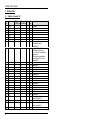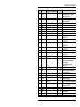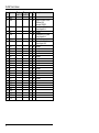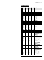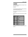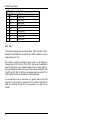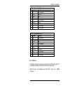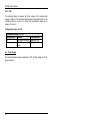
1
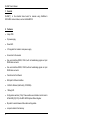
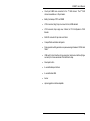
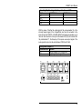
EVANET User's Manual EVANET User's Manual Copyright 2002,2003: FS Forth-Systeme GmbH Postfach 1103, 79200 Breisach, Germany Release of Document: Filename: Author: Board Revision February 5, 2003 EVANETu.doc D. Fögele, J. Jaeger, S. Lorenz EVANET_1 All rights reserved. No part of this document may be copied or reproduced in any form or by any means without the prior written consent of FS Forth-Systeme GmbH. 2 EVANET User's Manual Table of Contents 1. General............................................................................................................... 4 2. Features ............................................................................................................. 4 3. Module Pins........................................................................................................ 6 3.1. System Connector X2.............................................................................. 6 3.2. Peripheral Connector X3 ......................................................................... 9 4. Detailed Description......................................................................................... 13 4.1. JTAG Connector .................................................................................... 13 4.2. Serial Interfaces ..................................................................................... 15 4.2.1. RS232........................................................................................ 15 4.2.2. CAN............................................................................................ 16 4.2.3. Ethernet ..................................................................................... 17 4.2.4. USB............................................................................................ 18 4.3. Power Supply......................................................................................... 18 4.4. Battery Back-up ..................................................................................... 19 4.5. System Configuration ............................................................................ 20 4.6. User Area ............................................................................................... 21 4.7. CompactFlash........................................................................................ 25 4.7.5. CompactFlash, 50-pin connector X14....................................... 26 5. Changes to Revision EVANET_0.................................................................... 28 3 EVANET User's Manual 1. General EVANET_1 is the standard base board for modules using NetSilicon’s NET+ARM microcontrollers, such as the ModNET50. 2. Features • 4-layer PCB • 5V power supply • Power LED • 3.3V regulator for module’s main power supply • Connectors for the module • One serial interface RS232, COM A, with all handshaking signals on 9-pin SUBD male connector • One serial interface RS232, COM B, without handshaking signals on 9-pin SUBD male connector • Transformer for the Ethernet. • RJ45 jack for Ethernet interface • 2 LEDs for Ethernet (Link/Activity, 10/100Mbit). • 1 Debug LED • Configuration switches (7 bits). These switches are latched at end of reset to bit field GEN_ID[4-10] in the NET+ARM’s System Status Register. • Dip switch to select between little-endian and big-endian • Jumper to disable Flash memory 4 EVANET User's Manual • One 9-pin SUBD male connector for the 1st CAN channel. The 2nd CAN channel is available on a 10-pin header. • Battery for backup of RTC and SRAM • JTAG connector, Berg 14-pin, dual row 2.54 mm, ARM standard • JTAG connector, 8-pin single row, 2.54mm, for FS Forth-Systeme’s JTAG Booster • Multi-ICE connector 20-pin dual row 2.54mm • CompactFlash card holder with ejector • Pulse generator which generates a square-wave signal between 1300Hz and 14kHz • USB ports for host interface (A-type connector) and device interface (B-type connector) for future derivatives of the NetSilicon chips. • Reset push button • 4 user-definable push buttons • 4 user-definable LEDs • buzzer • optional graphic controller adaptable 5 EVANET User's Manual 3. Module Pins 3.1. System Connector X2 CS5# CS6# CS7# GND GND GND GND LITEND# 2nd func. On NET+50 - 3rd func. Type On NET+50 O O O P P P P I 5V tol. No 6 CSMODE - - I Yes 7 9 11 13 15 17 19 21 23 25 27 29 31 33 35 36 A0 A1 A2 A3 A4 A5 A6 A7 A8 A9 A10 A11 A12 A13 A14 CFG4 - - O O O O O O O O O O O O O O O I Yes Yes Yes Yes Yes Yes Yes Yes Yes Yes Yes Yes Yes Yes Yes No 37 38 A15 CFG5 - - O I Yes No 39 RSTIN# - - I No Pin X21 2 3 4 5 Signal 6 Description Reserved Reserved Reserved Low -> Little-Endian, not available on module ModNET50_0 High -> CS3# and CS4# available for external use Low -> CS4# only available for external use This signal is not available on modules ModNET50_0 and ModNET50_1 Address Bus Address Bus Address Bus Address Bus Address Bus Address Bus Address Bus Address Bus Address Bus Address Bus Address Bus Address Bus Address Bus Address Bus Address Bus Connected to A13, = System Status Register Bit 4 Address Bus Connected to A14, = System Status Register Bit 5 Reset input EVANET User's Manual Pin X240 Signal CFG6 2nd func. 3rd func. Type 5V On NET+50 On NET+50 tol. I No 41 42 PWRGOOD CFG7 - - O I No No 43 44 45 47 49 51 54 GND GND A16 A17 A18 A19 TRST# - - P P O O O O I Yes Yes Yes Yes No 56 TCK - - I No 58 TMS - - I No 60 TDI - - I No 61 62 WE# TDO - - O O Yes No 63 64 OE# FLSH_DIS - - O I Yes No 65 66 R/W# TS# - - O O Yes No 67 68 69 BCLK TA# CS3# - - O O O Yes No Yes 70 71 TEA# CS4# TLAST# - - O O No Yes 72 73 74 75 76 BG# BE2# BR# BE3# BUSY# - - I/O O I/O O I/O No Yes No Yes No Description Connected to A15, = System Status Register Bit 6 Output of the reset controller Connected to A16, = System Status Register Bit 7 Address Bus Address Bus Address Bus Address Bus JTAG, not available on module ModNET50_0 JTAG, not available on module ModNET50_0 JTAG, not available on module ModNET50_0 JTAG, not available on module ModNET50_0 JTAG, not available on module ModNET50_0 Disable Flash on module. Needed to enter debugger, if Flash is empty. Not available on module ModNET50_0 Transfer Start, not available on module ModNET_0 System Clock Data Transfer Acknowledge External chip select, see signal CSMODE Data Transfer Error Acknowledge External chip select, see signal CSMODE Bus Grant Bus Request Bus Busy 7 EVANET User's Manual GND CS2# 2nd func. On NET+50 - 3rd func. Type On NET+50 P O 5V tol. Yes 80 CFG8 - - I No 81 82 D16 CFG9 - - I/O I Yes No 83 84 D17 CFG10 - - I/O I Yes No 85 87 89 91 93 95 97 99 101 103 105 107 109 111 113 114 115 116 117 118 119 120 D18 D19 D20 D21 D22 D23 D24 D25 D26 D27 D28 D29 D30 D31 GND GND GND GND +3.3V +3.3V +3.3V +3.3V - - I/O I/O I/O I/O I/O I/O I/O I/O I/O I/O I/O I/O I/O I/O P P P P P P P P Yes Yes Yes Yes Yes Yes Yes Yes Yes Yes Yes Yes Yes Yes - Pin X277 79 Signal 8 Description Used on the module to select SRAM and CAN, see signal CSMODE Connected to A17, = System Status Register Bit 8 Data Bus Connected to A18, = System Status Register Bit 9 Data Bus Connected to A19, = System Status Register Bit 10 Data Bus Data Bus Data Bus Data Bus Data Bus Data Bus Data Bus Data Bus Data Bus Data Bus Data Bus Data Bus Data Bus Data Bus EVANET User's Manual 3.2. Peripheral Connector X3 Pin X31 2 3 4 5 6 7 8 9 10 11 12 13 14 15 16 17 18 19 20 21 Signal GND GND +5V +5V PORTA0 PORTA1 PORTA2 PORTA3 PORTA4 PORTA5 PORTA6 PORTA7 PORTB0 PORTB1 PORTB2 PORTB3 PORTB4 PORTB5 PORTB6 PORTB7 PORTC0 2nd func. On NET+50 DCDA# CTSA# DSRA# RXDA RXCA# RTSA# DTRA# TXDA DCDB# CTSB# DSRB# RXDB RXCB RTSB# DTRB# TXDB CI0 22 23 24 PORTC1 PORTC2 PORTC3 CI1 CI2 CI3 25 PORTC4 26 3rd func. On NET+50 DONE1# DACK1# OUT1A# DREQ1# DONE2# RPSF# DACK2# OUT1B# REJECT# DREQ2# Type 5V tol. P P P P I/O No I/O No I/O No I/O No I/O No I/O No I/O No I/O No I/O No I/O No I/O No I/O No I/O No I/O No I/O No I/O No I/O No AMUX I/O I/O I/O No No No RIB# RESET# I/O No PORTC5 TXCB OUT2B# I/O No 27 PORTC6 RIA# IRQ# I/O No 28 29 PORTC7 PORTD0 TXCA OUT2A# I/O I/O No - Description COM A, DCD# COM A, CTS# COM A, DSR# COM A, RXD Debug LED COM A, RTS# COM A, DTR# COM A, TXD REG#/IOIS16# COM B, RXD COM B, TXD ModNET50_0/ModNET50_1: Used as Interrupt Input from PHY ModNET50_2: Used for SDRAM reset bug fix Used as Interrupt Input from RTC Used as Interrupt Input from CAN Used as Interrupt Input from NE556 or CompactFlash ModNET50_0: Reset Output to PHY and CAN-Controller ModNET50_1: Reset for CAN-Controller ModNET50_0: I2CCLK, Used as I²C clock ModNET50_1: free ModNET50_0: Used for SDRAM reset bug fix ModNET50_1: I2CCLK, Used as I²C clock I2CDAT, Used as I²C data Reserved for NET+150 9 EVANET User's Manual Pin X330 31 32 33 34 35 36 37 38 39 40 41 42 43 44 45 46 47 Signal PORTD1 PORTD2 PORTD3 PORTD4 PORTD5 PORTD6 PORTD7 PORTE0 PORTE1 PORTE2 PORTE3 PORTE4 PORTE5 PORTE6 PORTE7 GND GND TPIP2 2nd func. 3rd func. Type 5V On NET+50 On NET+50 tol. I/O I/O I/O I/O I/O I/O I/O I/O I/O I/O I/O I/O I/O I/O I/O P P I - 48 49 TPIP1 TPIN2 - - I I - 50 51 TPIN1 TPOP2 - - I O - 52 53 TPOP1 TPON2 - - O O - 54 55 TPON1 LEDLNK2 - - O O - 56 57 LEDLNK1 LEDH2 - - O O - 58 59 LEDH1 ESD2 - - O I - 60 61 ESD1 EVCC2 - - I P - 62 EVCC1 - - P - 10 Description Reserved for NET+150 Reserved for NET+150 Reserved for NET+150 Reserved for NET+150 Reserved for NET+150 Reserved for NET+150 Reserved for NET+150 Reserved for NET+150 Reserved for NET+150 Reserved for NET+150 Reserved for NET+150 Reserved for NET+150 Reserved for NET+150 Reserved for NET+150 Reserved for NET+150 Reserved for NET+150, Ethernet 2 Input+ Ethernet 1 Input+ Reserved for NET+150, Ethernet 2 InputEthernet 1 InputReserved for NET+150, Ethernet 2 Output+ Ethernet 1 Output+ Reserved for NET+150, Ethernet 2 OutputEthernet 1 OutputReserved for NET+150, Ethernet 2 Line/Activity LED Ethernet 1 Line/Activity LED Reserved for NET+150, Ethernet 2 10/100 Mbit LED Ethernet 1 10/100 Mbit LED Reserved for NET+150, Ethernet 2 Signal detect Ethernet 1 Signal detect Reserved for NET+150, Ethernet 2 VCC, used for magnetics Ethernet 1 VCC, used for magnetics EVANET User's Manual Pin X363 Signal EGND2 2nd func. 3rd func. Type 5V On NET+50 On NET+50 tol. P - 64 65 66 67 68 69 70 71 72 73 74 75 76 77 78 79 80 81 82 83 84 85 86 87 88 89 90 91 92 93 94 95 96 97 98 99 100 101 102 103 EGND1 PACK# CANH/TXDA PEN# CANL/RXDA PINT1# CANH/TXDB PINT2# CANL/RXDB GND GND PDATA0 PA0 PDATA1 PA1 PDATA2 PA2 PDATA3 PA3 PDATA4 PA4 PDATA5 PA5 PDATA6 PA6 PDATA7 PA7 PDATA8 PA8 PDATA9 PA9 PDATA10 PA10 PDATA11 PA11 PDATA12 PA12 PDATA13 PA13 PDATA14 PCLKD1 PCLKD2 PCLKD3 PCLKD4 ACK1# ACK2# ACK3# ACK4# BUSY1 BUSY2 BUSY3 BUSY4 POE1# PE1 POE2# PE2 POE3# PE3 POE4# PE4 PCLKC1# PSELECT1 PCLKC2# PSELECT2 PCLKC3# GPIOF7 GPIOF6 GPIOF5 GPIOF4 GPIOD0 GPIOH0 GPIOD1 GPIOH1 GPIOD2 GPIOH2 GPIOD3 GPIOH3 GPIOD4 GPIOH4 GPIOD5 GPIOH5 GPIOD6 GPIOH6 GPIOD7 GPIOH7 GPIOG0 GPIOG1 GPIOG2 GPIOG3 GPIOG4 GPIOF3 - P I/O I/O I/O I/O I/O I/O I/O I/O P P I/O I/O I/O I/O I/O I/O I/O I/O I/O I/O I/O I/O I/O I/O I/O I/O I/O I/O I/O I/O I/O I/O No Yes No Yes No Yes No Yes No No No No No No No No No No No No No No No No No No No No No No No No No No No No No Description Reserved for Ethernet 2 GND Ethernet 1 GND CAN_TXD or CANH, channel A CAN_RXD or CANL, channel A CAN_TXD or CANH, channel B CAN_RXD or CANL, channel B 11 EVANET User's Manual Pin X3104 105 106 107 108 109 110 111 112 113 114 115 116 117 118 119 120 12 Signal PA14 PDATA15 PA15 PCS# PA16 PRW# USBP PBRW# USBN GND GND GND GND +3.3V VBAT +3.3V VBAT 2nd func. On NET+50 PSELECT3 PCLKC4# PSELECT4 FAULT2# FAULT1# FAULT3# FAULT4# - 3rd func. On NET+50 GPIOF2 GPIOG5 GPIOG7 GPIOG6 GPIOF0 GPIOF1 - Type 5V tol. I/O No No I/O No I/O No I/O No I/O No I/O I/O No I/O P P P P P P P P - Description Reserved for USB data + Reserved for USB data - For backup of SRAM and RTC For backup of SRAM and RTC EVANET User's Manual 4. Detailed Description 4.1. JTAG Connector There are three connectors to adapt to the JTAG interface of the NET+ARM CPUs: The 1st is the ARM standard 14-pin connector. The 2nd connector with 8 pins can be used to interface to the FS Forth-Systeme JTAG Booster. The 3rd connector with 20 pins is the Multi-ICE interface. 14-pin connector, X4 Pin Signal Function 1 +3.3V Power Supply for Adapter 3 NC Not connected 5 TDI Serial data input, to NET+ARM 7 TMS Serial mode select 9 TCK Serial clock 11 TDO Serial data output, from NET+ARM 13 +3.3V Power Supply for Adapter 2 GND GND 4 GND GND 6 GND GND 8 GND GND 10 GND GND 12 TRST# JTAG reset 1.) 14 GND GND 1.) Per default the signal TRST# is not connected to the module, because there is a connection between TRST# and the system reset already on the module. 13 EVANET User's Manual 8 pin connector, X5 Pin Signal Function 1 TCK Serial clock 2 GND GND 3 TMS Serial mode select 4 TRST# JTAG reset 5 NC Not connected 6 TDI Serial data input, to NET+ARM 7 TDO Serial data output, from NET+ARM 8 +3.3V Power supply for JTAG Booster 20 pin connector, X6 Pin Signal 1 +3.3V 3 TRST# 5 TDI 7 TMS 9 TCK 11 RTCK 13 TDO 15 POWERGOOD 17 NC 19 NC 2 +3.3V 4 GND 6 GND 8 GND 10 GND 12 GND 14 GND 16 GND 18 GND 20 GND 14 Function Reference power with current limitation JTAG reset Serial data input, to NET+ARM Serial mode select Serial clock Serial clock return path Serial data output, from NET+ARM System reset Not connected Not connected Power supply for adapter GND GND GND GND GND GND GND GND GND EVANET User's Manual 4.2. Serial Interfaces The Evaluation Board provides different kinds of serial interfaces. These are RS232, CAN, Ethernet and USB. 4.2.1. RS232 The Evaluation Board provides two RS232-interfaces; COM A and COM B. Both interfaces are fitted with 9-pin SUBD male connectors. COM A is fully equipped with all handshake signals. So a modem connection can be easy supported. COM B only provides the data lines TXD and RXD, without any handshake signals. COM A, 9-pin connector, X7 Pin Signal Function 1 DCD# Data Carrier Detect 2 RXD Receive data 3 TXD Transmit data 4 DTR# Data Terminal ready 5 GND GND 6 DSR# Data Set ready 7 RTS# Request to send 8 CTS# Clear to send 9 RI# Ring indicator 1.) 1.) RI# is connected to the RS232 driver, but the signal cannot be monitored by any CPU pin. 15 EVANET User's Manual COM B, 9-pin connector, X8 Pin Signal Function 1 NC Not connected 2 RXD Receive data 3 TXD Transmit data 4 NC Not connected 5 GND GND 6 NC Not connected 7 NC Not connected 8 NC Not connected 9 NC Not connected 4.2.2. CAN The Evaluation Board provides two CAN interfaces; CAN1 and CAN2. CAN1 is fitted with a 9-pin SUBD male connector X9, while CAN2 is available at a 10-pin header with twin rows, X10. Both channels provide the termination resistor, which can be disabled by removing jumper JP4 for CAN1 or JP5 for CAN2. There is also the possibility to place the CAN drivers on the Evaluation Board (this is the factory default), in case a module without CAN drivers is used. In this case the resistors R65, R70 for CAN1 and R81, R82 for CAN2, are not equipped and the resistors R71 for CAN1 and R83 for CAN2 are assembled on the Evaluation Board. It is also possible to insert an opto-coupler for a galvanic isolation of the CAN channels. This can be done by removing R72, R73 for CAN1 or R84, R85 for CAN2 and connecting the wire from the opto-coupler to the pads of these resistors. 16 EVANET User's Manual CAN 1, 9-pin connector, X9 Pin Signal Function 1 NC Not connected 2 CAN_L1 CAN low 3 GND GND 4 NC Not connected 5 NC Not connected 6 GND GND 7 CAN_H1 CAN high 8 NC Not connected 9 NC Not connected CAN 2, 10 pin connector, X10 Pin Signal Function 1 NC Not connected 3 CAN_L2 CAN low 5 GND GND 7 NC Not connected 9 NC Not connected 2 GND GND 4 CAN_H2 CAN high 6 NC Not connected 8 NC Not connected 10 NC Not connected 4.2.3. Ethernet The Ethernet connection is realized by a standard 8-pin RJ45 module jack, X11. For additional information about the data flow, there are two LEDs. LED LE2 shows the Link/Activity and LED LE3 is active for a 100Mbit connection. 17 EVANET User's Manual 4.2.4. USB The Evaluation Board is prepared for future versions of the module which support a USB port. The Evaluation Board provides the possibility either to use the USB channel as a host or as a device. This functionality is chosen by the jumpers J13 and J14. Configuration Jumper J13, J14 Configuration Jumper J13, J14 Connected Pins Function Used connector 1-2 NET+ARM is USB host USB type A, X12 2-3 NET+ARM is USB USB type B, X13 device 4.3. Power Supply The Evaluation Board expects a stabilized 5 VDC (±0.25V) voltage at the X1 power connector. 18 EVANET User's Manual 4.4. Battery Back-up A Lithium battery (3V) is also included on the Evaluation Board when shipped. It supplies both, low-powered SRAMs and the RTC on the module. According to the position of jumper J1 the battery can be connected or disconnected. Configuration Jumper J1 Connected Pins Function 1-2 Battery connected 2-3 Battery disconnected 19 EVANET User's Manual 4.5. System Configuration With the DIP switch S1 some configurations for the NET+ARM CPU can be made. The ON position generates a low-level at the CPU pin. Configuration DIP switch S1 Switch Function when ON 1 CFG4 written to system status register bit4 2 CFG5 written to system status register bit5 3 CFG6 written to system status register bit6 4 CFG7 written to system status register bit7 5 CFG8 written to system status register bit8 6 CFG9 written to system status register bit9 7 CFG10 written to system status register bit10 8 Little Endian With the jumper J2 the Flash memory on the module can be disabled. This is needed to enter the debugger, if the Flash memory is empty, for example. If the jumper J2 is open, the Flash memory is enabled. Configuration Jumper J2 Connected Pins Function 1-2 Flash memory disabled 20 EVANET User's Manual 4.6. User Area The Evaluation Board provides two expansion headers, 2x32 pins each (X16 and X17), with system and peripheral signals, a wire-wrap field, four LEDs, four push buttons, one potentiometer, one buzzer and a pulse generator; all of which can be freely used by the user. 21 EVANET User's Manual Expansion connector X17(AB), X16(CD) Pin 1 2 3 4 5 6 7 8 9 10 11 12 13 14 15 16 17 18 19 20 21 22 23 24 25 26 27 28 29 30 31 32 22 Row A Address A0 Address A2 Address A4 Address A6 Address A8 Address A10 Address A12 Address A14 Address A16 Address A18 RSTIN# WE# R/W# BCLK CS3# CS4# BE2# BE3# CS2# Data D16 Data D18 Data D20 Data D22 Data D24 Data D26 Data D28 Data D30 Row B Address A1 Address A3 Address A5 Address A7 Address A9 Address A11 Address A13 Address A15 Address A17 Address A19 PWRGOOD OE# TS# TA# TEA# BG# BR# BUSY# + 3,3V GND + 5V + 3,3V GND + 5V Data Data Data Data Data Data Data Data D17 D19 D21 D23 D25 D27 D29 D31 Row C Port A0 Port A2 Port A4 Port A6 Port B0 Port B2 Port B4 Port B6 Port C0 Port C2 Port C4 Port C6 PACK# PINT1# PDATA0 PDATA1 PDATA2 PDATA3 PDATA4 PDATA5 PDATA6 PDATA7 PDATA8 PDATA9 PDATA10 PDATA11 PDATA12 PDATA13 PDATA14 PDATA15 PCS# PRW# Row D Port A1 Port A3 Port A5 Port A7 Port B1 Port B3 Port B5 Port B7 Port C1 Port C3 Port C5 Port C7 PEN# PINT2# PA0 PA1 PA2 PA3 PA4 PA5 PA6 PA7 PA8 PA9 PA10 PA11 PA12 PA13 PA14 PA15 PA16 PBRW# EVANET User's Manual Generating Chip Select signals for the push buttons and LEDs Signal CETAST# active CELED# active A11 1 0 A12 1 1 CS3# 0 0 OE# 0 X With the jumper J18 either the output signal of the pulse generator U3 or the interrupt request signal of the CompactFlash card can be connected to the interrupt input port PORTC3 of the NET+ARM. If both signals are needed, one of them can be connected to a free port at the header X16 (CD) with a cable. With the potentiometer P1, the frequency of the square wave output signal of the pulse generator output can be varied between 1300Hz and 14kHz. Configuration Jumper J18 Connected Pins Function 1-2 Interrupt Request from CompactFlash 2-3 Output signal of pulse generator 23 EVANET User's Manual The four push buttons are not connected directly to port pins of the NET+ARM, but can be accessed by reading an 8-bit value from the address selected with CETAST#. The 8-bit value has the following meaning: Bit7 0 Bit6 0 Bit5 CD2# Bit4 CD1# Bit3 S11 Bit2 S10 Bit1 S9 Bit0 S8 CD1# and CD2# are the card detect signals of the CompactFlash card. The four LEDs are not connected directly to port pins of the NET+ARM, but can be accessed by writing an 8-bit value to the address selected with CELED#. The 8-bit value has the following meaning: Bit7 NC Bit6 NC Bit5 NC Bit4 NC Bit3 LE7 Bit2 LE6 Bit1 LE5 Bit0 LE4 Like the debug LED, the buzzer H1 is also connected to PORTA4. The buzzer can be disconnected by removing the jumper JP6. Configuration Jumper J6 Connected Pins Function 1-2 Buzzer connected 24 EVANET User's Manual 4.7. CompactFlash The Evaluation Board is equipped with a CFA Type 2 connector, X14, which is on the underside of the board. The card can only be accessed as a Master in True IDE mode. Generating Chip Select signals CEIDE1# and CEIDE2# Signal CEIDE1# active CEIDE2# active A11 0 1 A12 0 0 CS3# 0 0 OE# X X The card detect signals CD1# and CD2# can be read with the CETAST# chip select at Bit5 and Bit4 (see chapter 4.6). When both bits are set to zero, the card is inserted. 25 EVANET User's Manual 4.7.5. CompactFlash, 50-pin connector X14 Pin 1 2 3 4 5 6 7 Signal name True IDE mode GND D3 D4 D5 D6 D7 CEIDE1# 8 9 10 11 12 13 14 15 16 17 18 19 20 21 22 23 24 25 26 27 28 29 30 31 32 A10 ATASEL# A9 A8 A7 VCC A6 A5 A4 A3 A2 A1 A0 D0 D1 D2 IOIS16# CD2# CD1# D11 D12 D13 D14 D15 CEIDE2# 33 34 35 36 VS1# IORD# IOWR# WE# 26 Description GND Data D19 Data D20 Data D21 Data D22 Data D23 Card select signal 1 access to task file registers not used at True IDE mode low to select True IDE mode not used at True IDE mode not used at True IDE mode not used at True IDE mode + 3.3V not used at True IDE mode not used at True IDE mode not used at True IDE mode not used at True IDE mode Address A3 Address A2 Address A1 Data D16 Data D17 Data D18 not connected Card detect 2: high, if no card available Card detect 1: high, if no card available Data D27 Data D28 Data D29 Data D30 Data D31 Card select signal 2 access to alternate status register and device control register connected to +3.3V to read data in I/O task file area to write data in I/O task file area not used at True IDE mode EVANET User's Manual Pin 37 38 39 40 41 42 43 44 45 46 47 48 49 50 Signal name True IDE mode INTRQ VCC CSEL# VS2# RESET# IORDY INPACK# REG# DASP# PDIAG# D8 D9 D10 GND Description Interrupt request to the host (active high) + 3.3V low to select Master connected to +3.3V active low Reset signal connected to +3.3V not connected connected to +3.3V not connected not connected Data D24 Data D25 Data D26 GND 27 EVANET User's Manual 5. Changes to Revision EVANET_0 The following changes have been made: • removed the jumpers for the CompactFlash, the CompactFlash is now only accessible as Master at True IDE mode. • included a buzzer, connected to PORTA4 via jumper J6 • some wires have been taken over into the layout 28