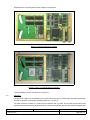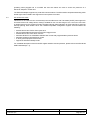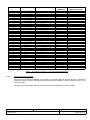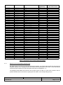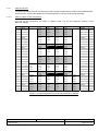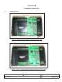
1
CCII Systems (Pty) Ltd Registration No. 1990/005058/07
C ommunications
C omputer I ntellig ence
I nteg ration
User Manual
for the
GPS + 7-Channel Serial I/O Adapter
and
8-Channel Serial I/O Adapter
C²I² Systems Document No.
CCII/LCP/6-MAN/007
Document Issue
1.1
Issue Date
2009-07-08
Print Date
2009-07-08
File Name
W:\LCP\TECH\MAN\CLCMAN07.wpd
Distribution List No.
© C²I² Systems The copyright of this document is the property of C²I² Systems. The document is issued for the sole
purpose for which it is supplied, on the express terms that it may not be copied in whole or part, used by
or disclosed to others except as authorised in writing by C²I² Systems.
Document prepared by and for C²I² Systems, Cape Town
Amendment History
Issue
Description
Date
ECP No.
1.0
Baseline
2009-03-25
-
1.1
Improve document naming consistency
2009-07-08
CCII/LCP/6-ECP/017
CCII/LCP/6-MAN/007
CLCMAN07.wpd
2009-07-08
Issue 1.1
Page iii of vi
Contents
1.
Introduction and Scope . . . . . . . . . . . . . . . . . . . . . . . . . . . . . . . . . . . . . . . . . . . . . . . . . . . . . 1
1.1
1.2
2.
Applicable and Reference Documents . . . . . . . . . . . . . . . . . . . . . . . . . . . . . . . . . . . . . . . . . 2
2.1
2.2
2.3
3.
3.2
3.3
3.4
3.5
3.6
3.7
3.8
3.9
3.10
3.11
3.12
3.13
3.14
3.15
System Overview . . . . . . . . . . . . . . . . . . . . . . . . . . . . . . . . . . . . . . . . . . . . . . . . . . . . . . . . . . . . . . . . . . . . . 3
3.1.1 GPS + 7-Channel Serial I/O Adapter . . . . . . . . . . . . . . . . . . . . . . . . . . . . . . . . . . . . . . . . . . . . . . . 3
3.1.2 8-Channel Serial I/O Adapter . . . . . . . . . . . . . . . . . . . . . . . . . . . . . . . . . . . . . . . . . . . . . . . . . . . . . 4
PMC Bus . . . . . . . . . . . . . . . . . . . . . . . . . . . . . . . . . . . . . . . . . . . . . . . . . . . . . . . . . . . . . . . . . . . . . . . . . . . 5
PCI 8-Channel UART . . . . . . . . . . . . . . . . . . . . . . . . . . . . . . . . . . . . . . . . . . . . . . . . . . . . . . . . . . . . . . . . . . 6
Configuration Space . . . . . . . . . . . . . . . . . . . . . . . . . . . . . . . . . . . . . . . . . . . . . . . . . . . . . . . . . . . . . . . . . . 7
PCI Interrupts . . . . . . . . . . . . . . . . . . . . . . . . . . . . . . . . . . . . . . . . . . . . . . . . . . . . . . . . . . . . . . . . . . . . . . . . 7
Configuration EEPROM . . . . . . . . . . . . . . . . . . . . . . . . . . . . . . . . . . . . . . . . . . . . . . . . . . . . . . . . . . . . . . . . 7
Complex Programmable Logic Device (CPLD) . . . . . . . . . . . . . . . . . . . . . . . . . . . . . . . . . . . . . . . . . . . . . . 8
GPS module . . . . . . . . . . . . . . . . . . . . . . . . . . . . . . . . . . . . . . . . . . . . . . . . . . . . . . . . . . . . . . . . . . . . . . . . . 8
GPS Antenna Connector . . . . . . . . . . . . . . . . . . . . . . . . . . . . . . . . . . . . . . . . . . . . . . . . . . . . . . . . . . . . . . . 8
RS-232 Transceivers . . . . . . . . . . . . . . . . . . . . . . . . . . . . . . . . . . . . . . . . . . . . . . . . . . . . . . . . . . . . . . . . . . 8
RS-485 Transceivers . . . . . . . . . . . . . . . . . . . . . . . . . . . . . . . . . . . . . . . . . . . . . . . . . . . . . . . . . . . . . . . . . . 9
Serial Channel Configuration DIP Switch S6 . . . . . . . . . . . . . . . . . . . . . . . . . . . . . . . . . . . . . . . . . . . . . . . . 9
3.12.1 GPS + 7-Channel Serial I/O Adapter . . . . . . . . . . . . . . . . . . . . . . . . . . . . . . . . . . . . . . . . . . . . . . . 9
3.12.2 8-Channel Serial I/O Adapter . . . . . . . . . . . . . . . . . . . . . . . . . . . . . . . . . . . . . . . . . . . . . . . . . . . . 10
Signal Ground Configuration DIP Switch S5 . . . . . . . . . . . . . . . . . . . . . . . . . . . . . . . . . . . . . . . . . . . . . . . 11
RS-485 Termination DIP Switches S1 to S4 . . . . . . . . . . . . . . . . . . . . . . . . . . . . . . . . . . . . . . . . . . . . . . . 12
PMC Connectors . . . . . . . . . . . . . . . . . . . . . . . . . . . . . . . . . . . . . . . . . . . . . . . . . . . . . . . . . . . . . . . . . . . . 13
3.15.1 PMC Pn4 Rear I/O Pin Assignments . . . . . . . . . . . . . . . . . . . . . . . . . . . . . . . . . . . . . . . . . . . . . . 13
Serial Interfaces . . . . . . . . . . . . . . . . . . . . . . . . . . . . . . . . . . . . . . . . . . . . . . . . . . . . . . . . . . 15
4.1
4.2
4.3
5.
Applicable Documents . . . . . . . . . . . . . . . . . . . . . . . . . . . . . . . . . . . . . . . . . . . . . . . . . . . . . . . . . . . . . . . . . 2
Reference Documents . . . . . . . . . . . . . . . . . . . . . . . . . . . . . . . . . . . . . . . . . . . . . . . . . . . . . . . . . . . . . . . . . 2
Specifications . . . . . . . . . . . . . . . . . . . . . . . . . . . . . . . . . . . . . . . . . . . . . . . . . . . . . . . . . . . . . . . . . . . . . . . . 2
Architecture . . . . . . . . . . . . . . . . . . . . . . . . . . . . . . . . . . . . . . . . . . . . . . . . . . . . . . . . . . . . . . 3
3.1
4.
Scope . . . . . . . . . . . . . . . . . . . . . . . . . . . . . . . . . . . . . . . . . . . . . . . . . . . . . . . . . . . . . . . . . . . . . . . . . . . . . . 1
Introduction . . . . . . . . . . . . . . . . . . . . . . . . . . . . . . . . . . . . . . . . . . . . . . . . . . . . . . . . . . . . . . . . . . . . . . . . . 1
Overview . . . . . . . . . . . . . . . . . . . . . . . . . . . . . . . . . . . . . . . . . . . . . . . . . . . . . . . . . . . . . . . . . . . . . . . . . . 15
Line Driver Selection . . . . . . . . . . . . . . . . . . . . . . . . . . . . . . . . . . . . . . . . . . . . . . . . . . . . . . . . . . . . . . . . . 15
Universal Asynchronous Receiver Transmitter (UART) . . . . . . . . . . . . . . . . . . . . . . . . . . . . . . . . . . . . . . . 15
GPS Interface . . . . . . . . . . . . . . . . . . . . . . . . . . . . . . . . . . . . . . . . . . . . . . . . . . . . . . . . . . . . 16
5.1
5.2
5.3
5.4
5.5
5.6
5.7
5.8
Overview of the GPS Interface . . . . . . . . . . . . . . . . . . . . . . . . . . . . . . . . . . . . . . . . . . . . . . . . . . . . . . . . . 16
GPS Module Specifications . . . . . . . . . . . . . . . . . . . . . . . . . . . . . . . . . . . . . . . . . . . . . . . . . . . . . . . . . . . . 16
Architecture of GPS module . . . . . . . . . . . . . . . . . . . . . . . . . . . . . . . . . . . . . . . . . . . . . . . . . . . . . . . . . . . 16
Default Configuration . . . . . . . . . . . . . . . . . . . . . . . . . . . . . . . . . . . . . . . . . . . . . . . . . . . . . . . . . . . . . . . . . 17
Configuration . . . . . . . . . . . . . . . . . . . . . . . . . . . . . . . . . . . . . . . . . . . . . . . . . . . . . . . . . . . . . . . . . . . . . . . 17
External Backup Battery . . . . . . . . . . . . . . . . . . . . . . . . . . . . . . . . . . . . . . . . . . . . . . . . . . . . . . . . . . . . . . 17
Pulse Per Second Signal . . . . . . . . . . . . . . . . . . . . . . . . . . . . . . . . . . . . . . . . . . . . . . . . . . . . . . . . . . . . . . 17
GPS Module . . . . . . . . . . . . . . . . . . . . . . . . . . . . . . . . . . . . . . . . . . . . . . . . . . . . . . . . . . . . . . . . . . . . . . . . 17
Annexure A . . . . . . . . . . . . . . . . . . . . . . . . . . . . . . . . . . . . . . . . . . . . . . . . . . . . . . . . . . . . . . . . 18
SAMTEC MMCX to SMA Cable Assembly . . . . . . . . . . . . . . . . . . . . . . . . . . . . . . . . . . . . . . . . . . . . . . . . . . . . . . 18
Annexure B . . . . . . . . . . . . . . . . . . . . . . . . . . . . . . . . . . . . . . . . . . . . . . . . . . . . . . . . . . . . . . . . 19
Installation Instructions . . . . . . . . . . . . . . . . . . . . . . . . . . . . . . . . . . . . . . . . . . . . . . . . . . . . . . . . . . . . . . . . . . . . . . 19
CCII/LCP/6-MAN/007
CLCMAN07.wpd
2009-07-08
Issue 1.1
Page iv of vi
List of Tables
Table 1 : PCI Configuration Space . . . . . . . . . . . . . . . . . . . . . . . . . . . . . . . . . . . . . . . . . . . . . . . . . . . . . . . . . . . . . . . . . . 7
Table 2 : S6 Codes for the GPS + 7-Channel Serial I/O Adapter . . . . . . . . . . . . . . . . . . . . . . . . . . . . . . . . . . . . . . . . . . 10
Table 3 : S6 Codes for the 8-Channel Serial I/O Adapter . . . . . . . . . . . . . . . . . . . . . . . . . . . . . . . . . . . . . . . . . . . . . . . 11
Table 4 : Switch S5 RS-232 Ground Connections . . . . . . . . . . . . . . . . . . . . . . . . . . . . . . . . . . . . . . . . . . . . . . . . . . . . . 12
Table 5 : S1 to S4 RS-485 Termination Resistor Selection . . . . . . . . . . . . . . . . . . . . . . . . . . . . . . . . . . . . . . . . . . . . . . 12
Table 6 : Pn4 Pin Assignments for the 8-Channel Serial I/O Adapter . . . . . . . . . . . . . . . . . . . . . . . . . . . . . . . . . . . . . . 13
Table 7 : Pn4 Pin Assignments for the GPS + 7-Channel Serial I/O Adapter . . . . . . . . . . . . . . . . . . . . . . . . . . . . . . . . 14
Table 8 : GPS Module Specifications . . . . . . . . . . . . . . . . . . . . . . . . . . . . . . . . . . . . . . . . . . . . . . . . . . . . . . . . . . . . . . . 16
List of Figures
Figure 1 : Functional Block Diagram of the GPS + 7-Channel Serial I/O Adapter . . . . . . . . . . . . . . . . . . . . . . . . . . . . . . 3
Figure 2 : Functional Block Diagram of the 8-Channel Serial I/O Adapter . . . . . . . . . . . . . . . . . . . . . . . . . . . . . . . . . . . . 4
Figure 3 : 8-Channel Serial I/O Adapter . . . . . . . . . . . . . . . . . . . . . . . . . . . . . . . . . . . . . . . . . . . . . . . . . . . . . . . . . . . . . . 5
Figure 4 : GPS + 7-Channel Serial I/O Adapter . . . . . . . . . . . . . . . . . . . . . . . . . . . . . . . . . . . . . . . . . . . . . . . . . . . . . . . . 5
Figure 5 : GPS Receiver Block Diagram . . . . . . . . . . . . . . . . . . . . . . . . . . . . . . . . . . . . . . . . . . . . . . . . . . . . . . . . . . . . 16
Figure 6 : SAMTEC Custom Cable Assembly . . . . . . . . . . . . . . . . . . . . . . . . . . . . . . . . . . . . . . . . . . . . . . . . . . . . . . . . 18
Figure 7 : 8-Channel Serial I/O Adapter on PMC Host Carrier Card . . . . . . . . . . . . . . . . . . . . . . . . . . . . . . . . . . . . . . . 19
Figure 8 : GPS + 7-Channel Serial I/O Adapter on PMC Host Carrier Card . . . . . . . . . . . . . . . . . . . . . . . . . . . . . . . . . 19
CCII/LCP/6-MAN/007
CLCMAN07.wpd
2009-07-08
Issue 1.1
Page v of vi
Abbreviations and Acronyms
BIST
CC
CCPMC
CD
CEP
CPLD
CS
CTS
DGPS
DIP
DSR
DTR
EEPROM
GPS
HCC
I/O
INT
IRQ
LSB
MHz
MSB
NMEA
PCB
PCI
PMC
PPS
RI
RS-232
RS-485
RTCM
RTS
Rx
SA
Tx
UART
VHDL
VHSIC
Built-In Self Test
Conduction-Cooled
Conduction-Cooled PMC
Carrier Detect
Circular Error Probability
Complex Programmable Logic Device
Chip Select
Clear to Send
Differential GPS
Dual In-line Package
Data Set Ready
Data Terminal Ready
Electrically Erasable and Programmable Read Only Memory
Global Positioning System
Host Carrier Card
Input / Output
Interrupt
Interrupt Request
Least Significant Bit
MegaHertz
Most Significant Bit
National Marine Electronics Association
Printed Circuit Board
Peripheral Component Interconnect
PCI Mezzanine Card
Pulse Per Second
Ring Indicator
(Electronics Industries Association) Recommended Standard 232, or : EIA-232
(Electronics Industries Association) Recommended Standard 485, or : EIA-485
Radio Technical Commission for Maritime Services
Request To Send
Receive
Selective Availability
Transmit
Universal Asynchronous Receiver Transmitter
VHSIC Hardware Description Language
Very High Speed Integrated Circuit
CCII/LCP/6-MAN/007
CLCMAN07.wpd
2009-07-08
Issue 1.1
Page vi of vi
1.
Introduction and Scope
1.1
Scope
This document serves as a user manual for the GPS + 7-Channel Serial I/O Adapter and 8-Channel Serial I/O
Adapter.
1.2
Introduction
This Serial I/O Adapter incorporates a PCI to 8-Channel Serial UART Device and is available in either one of
two configurations :
•
•
Seven serial I/O channels with an integrated GPS module
Eight serial I/O channels (without GPS module)
Each serial channel’s external interface is user configurable in either RS-232 or RS-485 modes of operation.
Onboard programmable logic controls the adapter’s external serial interfaces. Serial channel configuration
(RS-232 or RS-485 electrical modes, RS-485 Multidrop mode and RS-485 Flow Control mode) is set by
entering a binary code on a configuration DIP switch.
Each serial channel has bus termination resistors which can be selectively switched in for proper RS-485 line
termination. This is done by asserting the appropriate DIP Switches for individual RS-485 differential signal
pairs.
CCII/LCP/6-MAN/007
CLCMAN07.wpd
2009-07-08
Issue 1.1
Page 1 of 19
2.
Applicable and Reference Documents
2.1
Applicable Documents
2.1.1
EXAR Corporation Datasheet, EXAR XR17D158 Universal (3.3V and 5V) PCI Bus Octal UART, Revision 1.2.2,
dated August 2005.
2.1.2
MAXIM Semiconductors Datasheet, MAX3080E-MAX3089E ±15kVESD-Protected, Fail-Safe, High-Speed
(10Mbps), Slew-Rate-Limited RS-485/RS-422 Transceivers, Revision 1, dated May 2006.
2.1.3
Texas Instruments Datasheet, SN65C3243, SN75C3243 3-V to 5.5-V Multichannel RS-232 Compatible Line
Driver/Receiver, Revision SLLS353G, dated November 2004.
2.1.4
u-blox AG, LEA-4A, LEA-4H, LEA-4M, LEA-4P, LEA-4R, LEA-4S, LEA-4T Antaris®4 GPS Modules Data Sheet,
Revision 1, dated 2007-05-25.
2.2
Reference Documents
None.
2.3
Specifications
2.3.1
PCI Special Interest Group, PCI Local Bus Specification, Rev. 2.3, dated 2002-03-29.
2.3.2
IEEE Standard Physical and Environmental Layers for PCI Mezzanine Cards (PMC) : PMC, P1386.1-2001,
dated 2001-06-14.
2.3.3
IEEE Standard for a Common Mezzanine Card (CMC) Family : CMC, P1386-2001, dated 2001-06-14.
2.3.4
ANSI/VITA 20-2001 American National Standard for Conduction Cooled PMC, approved 2001-08-31.
CCII/LCP/6-MAN/007
CLCMAN07.wpd
2009-07-08
Issue 1.1
Page 2 of 19
3.
Architecture
3.1
System Overview
The serial I/O interface of the Serial I/O Adapter is routed externally via the 64-pin PMC rear I/O connector,
Pn4. Having eight serial channels, this gives an I/O allocation of eight I/O lines per serial channel.
3.1.1
GPS + 7-Channel Serial I/O Adapter
On the GPS + 7-Channel Serial I/O Adapter, Channel H of the PCI-UART is dedicated to communication with
the onboard GPS module. The GPS unit supports the reception of Differential GPS (DGPS) correction data via
the Channel H external serial I/O interface. This external interface is configurable in either RS-232 or RS-485
modes of operation and is controlled by the Channel H mode setting.
The GPS unit has a dedicated, programmable Pulse Per Second (PPS) output, available offboard to the user
via the Channel H external interface as either an RS-232 or RS-485 signal. This PPS signal is connected to
a hardware counter on the PCI-UART device as well, which could in turn be configured to generate an interrupt
after a user-specified amount of PPS ticks.
A permanent external signal ground connection is made via Pin 47 on Pn4, which is the ground reference for
offboard RS-232 signalling, as well as being the common ground connection used by the optional external GPS
backup battery (refer to Table 7).
The onboard GPS module connects to an external active GPS antenna via a supplied “pigtail” cable assembly.
Two slots in the adapter’s PCB provide maximum flexibility for routing the antenna cable offboard. An optional
external backup battery can be connected to the GPS unit (via the Pn4 rear I/O connector), which would aid
the GPS module in achieving faster GPS fixes after a system restart.
Block diagram of the GPS + 7-Channel Serial I/O adapter is shown in Figure 1.
PMC Bus
14,7456 MHz
Clock
Serial Mode
DIP Switch S6
Termination
Resistors
Termination
DIP Switches
S1 to S4
Enable Lines
PCI
PCI
8-Channel
UART
Channels A to G
Ch. H
GPS
Module
PPS
Bus
Mode Decoding
Logic
DGPS+PPS
RS-232
Transceivers
(Ch. A to G)
RS-485
Transceivers
(DGPS+PPS)
RS-232
Transceiver
(DGPS+PPS)
EEPROM
(optional)
Rear I/O Connector
RS-485
Transceivers
(Ch. A to G)
CPLD
GPS backup battery
GPS
Antenna
Connector
Figure 1 : Functional Block Diagram of the GPS + 7-Channel Serial I/O Adapter
CCII/LCP/6-MAN/007
CLCMAN07.wpd
2009-07-08
Issue 1.1
Page 3 of 19
3.1.2
8-Channel Serial I/O Adapter
On the 8-Channel Serial I/O Adapter, Channels A to G each provide the eight standard modem signals (Tx, Rx,
CTS, RTS, DSR, DTR, RI and CD) in RS-232 mode. Channel H has a reduced number of signals in RS-232
mode (only Tx, Rx, CTS and RTS), due to the external signal ground connection (shared by all RS-232
channels) taking up four pins on the Channel H external I/O interface.
The RS-232 signal ground lines are manually connected / disconnected using DIP Switch S5. This is different
from the configuration found on the GPS + 7-Channel Serial I/O Adapter, where a single permanent external
ground connection is made via Pin 47 on connector Pn4. Care should be taken not to engage the S5 signal
ground connections if Channel H is configured in RS-485 mode, for the reason that these signal ground
connections and the Channel H RS-485 signals share the same Pn4 rear I/O pins (refer to Table 6).
In RS-485 mode, Tx, Rx, CTS and RTS signals are available on all of Channels A through H.
If at least one channel is configured in RS-232 mode, an external signal ground connection is required and will
have to be made via DIP Switch S5. Due to the fact that these signal ground lines are multiplexed with the
Channel H RS-485 signal I/O lines, RS-485 signalling will thus no longer be possible on Channel H once these
signal ground connections have been made. This implies that Channel H can only be configured in RS-485
mode if none of Channels A to G are configured in RS-232 mode either and thus no external signal ground
connection is required.
Conversely, should any one of Channels A to G be configured in RS-232 mode, then Channel H should also
be configured in RS-232 mode and the external signal ground connections should be made available via the
rear I/O connector. It follows that, when assigning RS-232 Channels, Channel H should be the first Channel
to elect for that role.
Block diagram of the 8-Channel Serial I/O Adapter is shown in Figure 2.
PMC Bus
14,7456 MHz
Clock
Serial Mode
DIP Switch S6
Termination
Resistors
Termination
DIP Switches
S1 to S4
Enable Lines
PCI
PCI
8-Channel
UART
Channels A to H
RS-485
Transceivers
(Ch. A to G)
RS-232
Transceivers
(Ch. A to G)
RS-485
Transceivers
(Ch. H)
Bus
Mode Decoding
Logic
RS-232
Transceiver
(Ch. H)
Rear I/O Connector
CPLD
EEPROM
(optional)
RS-232 Ground
DIP Switch S5
Figure 2 : Functional Block Diagram of the 8-Channel Serial I/O Adapter
CCII/LCP/6-MAN/007
CLCMAN07.wpd
2009-07-08
Issue 1.1
Page 4 of 19
Depicted below are photographs of both adapter configurations :
Figure 3 : 8-Channel Serial I/O Adapter
Figure 4 : GPS + 7-Channel Serial I/O Adapter
Typical installation photos are shown in Annexure B.
3.2
PMC Bus
The Serial I/O Adapter can be installed on any Host Carrier Card (HCC) conforming to the PMC specification
and which supports Universal PCI signalling (either 3,3 V or 5,0 V).
The PMC interface consists of a 32-bit PCI bus interface and a number of bus-mode signals. Bus-mode
signalling is implemented using dedicated logic ICs. Bus-mode signalling prevents the Serial I/O Adapter from
CCII/LCP/6-MAN/007
CLCMAN07.wpd
2009-07-08
Issue 1.1
Page 5 of 19
operating when plugged into a non-PMC slot and also allows the host to sense the presence of a
Serial I/O Adapter in a PMC slot.
The Serial I/O Adapter supports only 32-bit PCI communications. The PCI interface is implemented using a PCI
based eight-channel UART and supports PCI bus speeds of 33 MHz.
3.3
PCI 8-Channel UART
This device is an octal PCI bus Universal Asynchronous Receiver and Transmitter (UART) with support for
universal PCI bus I/O voltage levels, making it suitable for use in a wide range of 3,3 V and 5,0 V PCI hosts.
A global interrupt source register provides complete interrupt status indication for all 8 channels to speed up
interrupt parsing. Each UART has its own 16C550-compatible configuration register set and features the
following :
•
•
•
•
•
•
•
transmit and receive FIFOs of 64 bytes each
fully programmable transmit and receive FIFO trigger levels
transmit and receive FIFO level counters
automatic RTS/CTS or DTR/DSR hardware flow control with programmable hysteresis levels
automatic software (Xon/Xoff) flow control
a 16-bit general purpose timer/counter
support for RS-485 multidrop mode
For a detailed description of the PCI UART register interface and its operation, please refer to the XR17D158
UART Datasheet [2.1.1].
CCII/LCP/6-MAN/007
CLCMAN07.wpd
2009-07-08
Issue 1.1
Page 6 of 19
3.4
Configuration Space
The PCI interface defines a standard programming model for the configuration of PCI devices. This interface
is defined as the Configuration Space. Table 1 below shows the Configuration Space as defined by the PCI bus
specification :
AD31-23
AD22-16
AD15-8
AD7-0
Address
Device ID(0x0158)
Vendor ID(0x13AB)
0x00
Status
Command
0x04
Class Code(0x070002)
BIST
Header Type
Latency Timer
0x08
Cache Size(0x00)
0x0C
Memory Base Address Register (BAR)
0x10
Unimplemented Base Address Register
0x14
Unimplemented Base Address Register
0x18
Unimplemented Base Address Register
0x1C
Unimplemented Base Address Register
0x20
Unimplemented Base Address Register
0x24
Reserved
0x28
Subsystem ID
Max Latency(0x00)
Revision ID(0x01)
Subsystem Vendor ID
0x2C
Reserved
0x30
Reserved
0x34
Reserved
0x38
Min Grant(0x00)
Interrupt Pin(0x01)
Interrupt Line
0x3C
Table 1 : PCI Configuration Space
The location of the configuration registers is defined by the HCC at startup.
3.5
PCI Interrupts
The PMC Adapter supports interrupts on the INTA# pin only. This is reflected in the Interrupt Pin Register of
the Configuration Space, as defined in Table 1.
3.6
Configuration EEPROM
The PCI UART supports an optional EEPROM device to store the vendor and sub-vendor ID and adapter model
numbers. This information is only used during plug-and-play auto configuration of the PCI local bus, where this
data would facilitate automatic hardware installation onto the PCI bus.
The EEPROM interface consists of four signals, EEDI, EEDO, EECS, and EECK. The EEPROM is, however,
not needed when auto configuration is not required in the end application and is thus omitted from the default
build.
However, should the user application require non-volatile memory for other purposes it is possible to store and
retrieve data stored on the EEPROM through a special PCI device configuration register. For such applications
the adapter can be specially ordered with the EEPROM installed. Contact Support for further information.
CCII/LCP/6-MAN/007
CLCMAN07.wpd
2009-07-08
Issue 1.1
Page 7 of 19
3.7
Complex Programmable Logic Device (CPLD)
The electrical configuration of the adapter’s I/O interface is controlled by programmable logic implemented in
a CPLD. Tables 2 and 3 (refer to Paragraph 3.12) lists all available modes of operation for both versions of the
adapter. Each listed mode of operation has an associated binary code which can be entered into configuration
DIP Switch S6 to specify the adapter’s serial I/O configuration or “mode”.
Each serial channel is user configurable in either RS-232 or RS-485 modes of operation. The PCI-UART device
also supports RS-485 multidrop mode with user specifiable transmit / receive turn-around delays. Multidrop
mode is available on all RS-485 channels.
The Channel A to D RS-485 Channels can be extended to include the DSR and DTR flow control signals (in
addition to the standard CTS and RTS signals). Channel A can be extended even further in RS-485 mode, to
additionally make available the CD and RI signals as well.
Extending Channels A to D as described above however comes at the cost of sacrificing other serial I/O
channels, due to the limited overall number of rear I/O pins available on Pn4.
The CPLD control logic can be customised, should that be required for the application. Please contact Support
for further information.
3.8
GPS module
The GPS module on the GPS + 7-Channel Serial I/O Adapter is the u-blox LEA-4S Integrated GPS module.
It features a 4 Hz position update rate with a -157 dBm receiver sensitivity. It also supports the reception of
Differential GPS (DGPS) correction data. An external backup battery can be connected for faster GPS lock-on
during system restart (so called “warm” start).
Dedicated active antenna short circuit protection and open circuit detection circuitry is integrated onto the
Serial I/O Adapter. A Pulse Per Second (PPS) output from the GPS module is available offboard as either an
RS-232 or RS-485 signal, as well as being connected to a hardware counter on the PCI UART device itself.
An overview of the GPS unit’s operation and interface is given in Paragraph 5. For detailed information please
refer to the LEA-4S Datasheet [2.1.4].
3.9
GPS Antenna Connector
A straight female MMCX antenna connector is installed on the component side of the Serial I/O Adapter. A
mating right-angle male MMCX connector can swivel towards either one of two slots in the adapter’s PCB,
providing two distinct routing options for taking the antenna cable offboard.
A single 300 mm length male MMCX to female SMA “pigtail” cable is provided with the adapter (refer to
Annexure A). It is suggested that only original Samtec mating MMCX connectors be used to ensure a secure
fit and conformance to the I/O area height restriction of the ANSI/VITA 20-2001 standard [2.3.4].
For appropriate GPS active antenna selection, please refer to the u-blox AG, LEA-4S Datasheet [2.1.4].
3.10
RS-232 Transceivers
The eight onboard RS-232 transceivers are individually enabled / disabled under control of the CPLD. Each
can transmit / receive serial data at rates of up to 1 Mbit/s (which is the maximum data rate supported by the
RS-232 transceivers) over distances of up to ten metres.
The PCI UART device can however be configured to communicate at much faster data rates (up to 6,25 Mbit/s
per channel). Care should thus be taken to ensure that user software limits RS-232 data rates to a maximum
of 1 Mbit/s.
CCII/LCP/6-MAN/007
CLCMAN07.wpd
2009-07-08
Issue 1.1
Page 8 of 19
3.11
RS-485 Transceivers
The sixteen onboard RS-485 transceivers (two per serial channel) are also individually controlled by the CPLD
control logic. Each can transmit / receive serial data up to the maximum UART data rate of 6,25 Mbit/s over
distances of up to one hundred metres. Transmission distances of up to one kilometre are possible at lower
data rates.
3.12
Serial Channel Configuration DIP Switch S6
DIP Switch S6 is used as input to the CPLD to specify the serial channel configuration. Tables 2 and 3 list all
the available modes of operation for both versions of the adapter, specifying the binary code for each
configuration. Switch S6 uses Active Low signalling, thus a “0" in Tables 2 and 3 equates to the ON position
and a “1" equates to the OFF position. A binary code of “10000001" is thus keyed into Switch S6 as :
OFF-ON-ON-ON-ON-ON-ON-OFF.
3.12.1
GPS + 7-Channel Serial I/O Adapter
On the GPS + 7-Channel Serial I/O Adapter the Channel H line drivers (RS-232 and RS-485) are connected
to the GPS module’s external serial interface (DGPS and PPS signals). These line level serial I/O signals are
routed to the Aux port on Pn4, as shown in Table 7.
The Switch S6 configuration codes for the GPS + 7-Channel Serial I/O Adapter are given in Table 2.
Note that on the GPS + 7-Channel Serial I/O Adapter, Switch S6.1 (denoted by an “X” in Table 2) is used to
control the Channel H configuration independently from Channels A to G. In each case, setting Switch S6.1
to “0" (ON) would set Channel H to RS-232 mode and setting Switch S6.1 to “1" (OFF) would set Channel H to
RS-485 mode.
CCII/LCP/6-MAN/007
CLCMAN07.wpd
2009-07-08
Issue 1.1
Page 9 of 19
S6.1 to S6.8
X000
X001
X001
X010
X010
X010
X010
X011
X011
X011
X011
X011
X100
X100
X100
X100
X100
X101
X101
X101
X101
X101
X101
X101
X110
X110
X110
X110
X110
X110
X110
X110
X111
X111
X111
X111
X111
X111
X111
X111
X111
0000
0000
1000
0000
0001
1000
1001
0000
0001
1000
1001
1010
0000
1000
1001
1010
1011
0000
0001
1000
1001
1010
1011
1100
0000
0001
1000
1001
1010
1011
1100
1101
0000
0001
1000
1001
1010
1011
1100
1101
1110
RS-232
A to G, [H,X=0]
B to G, [H,X=0]
B to G, [H,X=0]
B to F, [H,X=0]
B to F, [H,X=0]
B to F, [H,X=0]
B to F, [H,X=0]
C to F, [H,X=0]
C to F, [H,X=0]
C to F, [H,X=0]
C to F, [H,X=0]
C to F, [H,X=0]
D to F, [H,X=0]
D to F, [H,X=0]
D to F, [H,X=0]
D to F, [H,X=0]
D to F, [H,X=0]
D to E, [H,X=0]
D to E, [H,X=0]
D to E, [H,X=0]
D to E, [H,X=0]
D to E, [H,X=0]
D to E, [H,X=0]
D to E, [H,X=0]
E, [H,X=0]
E, [H,X=0]
E, [H,X=0]
E, [H,X=0]
E, [H,X=0]
E, [H,X=0]
E, [H,X=0]
E, [H,X=0]
[H,X=0]
[H,X=0]
[H,X=0]
[H,X=0]
[H,X=0]
[H,X=0]
[H,X=0]
[H,X=0]
[H,X=0]
RS-485
[H,X=1]
A, [H,X=1]
[H,X=1]
A, G, [H,X=1]
[H,X=1]
G, [H,X=1]
[H,X=1]
A to B, G, [H,X=1]
[H,X=1]
B, G, [H,X=1]
B, [H,X=1]
[H,X=1]
A to C, G, [H,X=1]
B to C, G, [H,X=1]
B to C, [H,X=1]
C, [H,X=1]
[H,X=1]
A to C, F to G, [H,X=1]
[H,X=1]
B to C, F to G, [H,X=1]
B to C, F, [H,X=1]
C, F, [H,X=1]
F, [H,X=1]
[H,X=1]
A to D, F to G, [H,X=1]
[H,X=1]
B to D, F to G, [H,X=1]
B to D, F, [H,X=1]
C to D, F, [H,X=1]
D, F, [H,X=1]
D, [H,X=1]
[H,X=1]
A to G, [H,X=1]
[H,X=1]
B to G, [H,X=1]
B to F, [H,X=1]
C to F, [H,X=1]
D to F, [H,X=1]
D to E, [H,X=1]
E, [H,X=1]
[H,X=1]
RS-485
Multidrop
none
none
A
none
none
A
A, G
none
none
A
A, G
A to
none
A
A, G
A to
A to
none
none
A
A, G
A to
A to
A to
none
none
A
A, G
A to
A to
A to
A to
none
none
A
A, G
A to
A to
A to
A to
A to
B, G
B, G
C, G
B, G
C, G
C, F to G
B,
C,
C,
D,
G
G
F to G
F to G
B,
C,
C,
D,
G
G
G
F to G
F to G
RS-48445
With Flow Control
none
none
none
none
A
none
none
none
A to B
none
none
none
none
none
none
none
none
none
A to C
none
none
none
none
none
none
A to D
none
none
none
none
none
none
none
A (full Modem),B to D
none
none
none
none
none
none
none
Table 2 : S6 Codes for the GPS + 7-Channel Serial I/O Adapter
3.12.2
8-Channel Serial I/O Adapter
On the 8-Channel Serial I/O Adapter the Channel H line drivers (RS-232 and RS-485) are connected to
Channel H of the PCI-UART. The Channel H line level serial I/O signals are routed to the Aux port on Pn4, as
shown in Table 6.
The Switch S6 configuration codes for the 8-Channel Serial I/O Adapter are given in Table 3.
CCII/LCP/6-MAN/007
CLCMAN07.wpd
2009-07-08
Issue 1.1
Page 10 of 19
S6.1 to S6.8
0000
0001
0001
0010
0010
0010
0010
0011
0011
0011
0011
0011
0100
0100
0100
0100
0100
0101
0101
0101
0101
0101
0101
0101
0110
0110
0110
0110
0110
0110
0110
0110
0111
0111
0111
0111
0111
0111
0111
0111
0111
1111
1111
1111
1111
1111
1111
1111
1111
1111
1111
0000
0000
1000
0000
0001
1000
1001
0000
0001
1000
1001
1010
0000
1000
1001
1010
1011
0000
0001
1000
1001
1010
1011
1100
0000
0001
1000
1001
1010
1011
1100
1101
0000
0001
1000
1001
1010
1011
1100
1101
1110
0000
0001
1000
1001
1010
1011
1100
1101
1110
1111
RS-232
A to
B to
B to
B to
B to
B to
B to
C to
C to
C to
C to
C to
D to
D to
D to
D to
D to
D to
D to
D to
D to
D to
D to
D to
E, H
E, H
E, H
E, H
E, H
E, H
E, H
E, H
H
H
H
H
H
H
H
H
H
none
none
none
none
none
none
none
none
none
none
G,
G,
G,
F,
F,
F,
F,
F,
F,
F,
F,
F,
F,
F,
F,
F,
F,
E,
E,
E,
E,
E,
E,
E,
H
H
H
H
H
H
H
H
H
H
H
H
H
H
H
H
H
H
H
H
H
H
H
H
RS-485
none
A
none
A, G
none
G
none
A to
none
B, G
B
none
A to
B to
B to
C
none
A to
none
B to
B to
C, F
F
none
A to
none
B to
B to
C to
D, F
D
none
A to
none
B to
B to
C to
D to
D to
E
none
A to
H
B to
B to
C to
D to
D to
E, H
H
none
B, G
C, G
C, G
C
C, F to G
C, F to G
C, F
D, F to G
D, F to G
D, F
D, F
G
G
F
F
F
E
H
H
F,
F,
F,
E,
H
H
H
H
RS-485
Multidrop
none
none
A
none
none
A
A, G
none
none
A
A, G
A to
none
A
A, G
A to
A to
none
none
A
A, G
A to
A to
A to
none
none
A
A, G
A to
A to
A to
A to
none
none
A
A, G
A to
A to
A to
A to
A to
none
none
A
A, G
A to
A to
A to
A to
A to
A to
B, G
B, G
C, G
B, G
C, G
C, F to G
B,
C,
C,
D,
G
G
F to G
F to G
B,
C,
C,
D,
G
G
G
F to G
F to G
B,
C,
C,
D,
G
H
G
G
F to G
F to G
RS-485
with Flow Control
none
none
none
none
A
none
none
none
A to B
none
none
none
none
none
none
none
none
none
A to C
none
none
none
none
none
none
A to D
none
none
none
none
none
none
none
A (full Modem),B to D
none
none
none
none
none
none
none
none
A (full Modem),B to D
none
none
none
none
none
none
none
none
Table 3 : S6 Codes for the 8-Channel Serial I/O Adapter
3.13
Signal Ground Configuration DIP Switch S5
DIP Switch S5 is only found on the 8-Channel Serial I/O Adapter. It is used to make the RS-232 signal ground
available offboard, but is multiplexed with some Channel H RS-485 signals. None of S5.1 to S5.4 should be
closed (ON) when Channel H is set to RS-485 mode (refer to Paragraph 3.1.1).
The mapping of DIP Switch S5 to the Pn4 rear I/O pins is given in Table 4. In each case a switch in the ON
position indicates that a connection to signal ground is made on the corresponding Pn4 pin.
CCII/LCP/6-MAN/007
CLCMAN07.wpd
2009-07-08
Issue 1.1
Page 11 of 19
Switch (ON)
Pin on Pn4 Connected to Ground
S5.1
Pin 19 (Aux3)
S5.2
Pin 20 (Aux4)
S5.3
Pin 47 (Aux7)
S5.4
Pin 48 (Aux8)
Table 4 : Switch S5 RS-232 Ground Connections
3.14
RS-485 Termination DIP Switches S1 to S4
DIP Switches S1 through S4 are used to connect / disconnect the 100 Ω line termination resistors for each
RS-485 differential signal pair. Switch assignments are shown in Table 5. Individual switch assignments are
also printed on the Serial I/O Adapter’s primary side silkscreen for quick reference.
Switch (ON)
S1.1
S1.2
S1.3
S1.4
S1.5
S1.6
S1.7
S1.8
S2.1
S2.2
S2.3
S2.4
S2.5
S2.6
S2.7
S2.8
S3.1
S3.2
S3.3
S3.4
S3.5
S3.6
S3.7
S3.8
S4.1
S4.2
S4.3
S4.4
S4.5
S4.6
S4.7
S4.8
Signal Pair Being Terminated
A_RxD+/A_RxDA_TxD+/A_TxDA_CTS+/A_CTSA_RTS+/A_RTSB_RxD+/B_RxDB_TxD+/B_TxDB_CTS+/B_CTSB_RTS+/B_RTSC_RxD+/C_RxDC_TxD+/C_TxDC_CTS+/C_CTSC_RTS+/C_RTSD_RxD+/D_RxDD_TxD+/D_TxDD_CTS+/D_CTSD_RTS+/D_RTSE_RxD+/E_RxDE_TxD+/E_TxDE_CTS+/E_CTSE_RTS+/E_RTSF_RxD+/F_RxDF_TxD+/F_TxDF_CTS+/F_CTSF_RTS+/F_RTSG_RxD+/G_RxDG_TxD+/G_TxDG_CTS+/G_CTSG_RTS+/G_RTSAux_RxD+/Aux_RxDAux_TxD+/Aux_TxDAux_CTS+/Aux_CTSAux_RTS+/Aux_RTS-
Table 5 : S1 to S4 RS-485 Termination Resistor Selection
Note :
CCII/LCP/6-MAN/007
CLCMAN07.wpd
It is crucial that these termination resistors not be switched in for any serial I/O channels that have
been set to RS-232 operation.
2009-07-08
Issue 1.1
Page 12 of 19
3.15
PMC Connectors
The Serial I/O Adapter has two connectors (Pn1 and Pn2) which implement the 32-bit, 33 MHz PMC interface.
Connector Pn4 connects the adapter to the host backplane to route the serial signals externally.
3.15.1
PMC Pn4 Rear I/O Pin Assignments
Pn4 rear I/O pin assignments are shown in Tables 6 and 7 for the two respective versions of the
Serial I/O Adapter.
Pin Name
RS-485
RS-232
RS-232
RS-485
Pin Name
1
PORTA1
A_RxD+
A_RxD
A_TxD
A_TxD+
PORTA2
3
PORTA3
A_RxD-
A_CTS
A_RTS
A_TxD-
PORTA4
2
4
5
PORTA5
A_CTS+
A_DSR
A_DTR
A_RTS+
PORTA6
6
7
PORTA7
A_CTS-
A_RI
A_CD
A_RTS-
PORTA8
8
9
PORTB1
B_RxD+
B_RxD
B_TxD
B_TxD+
PORTB2
10
11
PORTB3
B_RxD-
B_CTS
B_RTS
B_TxD-
PORTB4
12
13
PORTB5
B_CTS+
B_DSR
B_DTR
B_RTS+
PORTB6
14
15
PORTB7
B_CTS-
B_RI
B_CD
B_RTS-
PORTB8
16
17
AUX1
H_RxD+
H_RxD
H_TxD
H_TxD+
AUX2
18
19
AUX3
H_RxD-
GND
GND
H_TxD-
AUX4
20
21
PORTC1
C_RxD+
C_RxD
C_TxD
C_TxD+
PORTC2
22
23
PORTC3
C_RxD-
C_CTS
C_RTS
C_TxD-
PORTC4
24
25
PORTC5
C_CTS+
C_DSR
C_DTR
C_RTS+
PORTC6
26
27
PORTC7
C_CTS-
C_RI
C_CD
C_RTS-
PORTC8
28
29
PORTD1
D_RxD+
D_RxD
D_TxD
D_TxD+
PORTD2
30
31
PORTD3
D_RxD-
D_CTS
D_RTS
D_TxD-
PORTD4
32
33
PORTD5
D_CTS+
D_DSR
D_DTR
D_RTS+
PORTD6
34
35
PORTD7
D_CTS-
D_RI
D_CD
D_RTS-
PORTD8
36
37
PORTE1
A_RI+
E_RxD+
E_RxD
E_TxD
E_TxD+
PORTE2
38
39
PORTE3
A_RI-
E_RxD-
E_CTS
E_RTS
E_TxD-
PORTE4
40
41
PORTE5
A_CD+
E_CTS+
E_DSR
E_DTR
E_RTS+
PORTE6
42
43
PORTE7
A_CD-
E_CTS-
E_RI
E_CD
E_RTS-
PORTE8
44
45
AUX5
H_CTS+
H_CTS
H_RTS
H_RTS+
AUX6
46
47
AUX7
H_CTS-
GND
GND
H_RTS-
AUX8
48
49
PORTF1
D_DSR+
F_RxD+
F_RxD
F_TxD
F_TxD+
D_DTR+
PORTF2
50
51
PORTF3
D_DSR-
F_RxD-
F_CTS
F_RTS
F_TxD-
D_DTR-
PORTF4
52
53
PORTF5
C_DSR+
F_CTS+
F_DSR
F_DTR
F_RTS+
C_DTR+
PORTF6
54
55
PORTF7
C_DSR-
F_CTS-
F_RI
F_CD
F_RTS-
C_DTR-
PORTF8
56
57
PORTG1
B_DSR+
G_RxD+
G_RxD
G_TxD
G_TxD+
B_DTR+
PORTG2
58
59
PORTG3
B_DSR-
G_RxD-
G_CTS
G_RTS
G_TxD-
B_DTR-
PORTG4
60
61
PORTG5
A_DSR+
G_CTS+
G_DSR
G_DTR
G_RTS+
A_DTR+
PORTG6
62
63
PORTG7
A_DSR-
G_CTS-
G_RI
G_CD
G_RTS-
A_DTR-
PORTG8
64
Table 6 : Pn4 Pin Assignments for the 8-Channel Serial I/O Adapter
CCII/LCP/6-MAN/007
CLCMAN07.wpd
2009-07-08
Issue 1.1
Page 13 of 19
Pin Name
RS-485
RS-232
RS-232
RS-485
Pin Name
1
PORTA1
A_RxD+
A_RxD
A_TxD
A_TxD+
PORTA2
3
PORTA3
A_RxD-
A_CTS
A_RTS
A_TxD-
PORTA4
4
5
PORTA5
A_CTS+
A_DSR
A_DTR
A_RTS+
PORTA6
6
7
PORTA7
A_CTS-
A_RI
A_CD
A_RTS-
PORTA8
8
9
PORTB1
B_RxD+
B_RxD
B_TxD
B_TxD+
PORTB2
10
11
PORTB3
B_RxD-
B_CTS
B_RTS
B_TxD-
PORTB4
12
13
PORTB5
B_CTS+
B_DSR
B_DTR
B_RTS+
PORTB6
14
15
PORTB7
B_CTS-
B_RI
B_CD
B_RTS-
PORTB8
16
17
AUX1
DGPS_Rx+
DGPS_Rx
DGPS_Tx
DGPS_Tx+
AUX2
18
19
AUX3
DGPS_Rx-
N/C
N/C
DGPS_Tx-
AUX4
20
21
PORTC1
C_RxD+
C_RxD
C_TxD
C_TxD+
PORTC2
22
23
PORTC3
C_RxD-
C_CTS
C_RTS
C_TxD-
PORTC4
24
25
PORTC5
C_CTS+
C_DSR
C_DTR
C_RTS+
PORTC6
26
27
PORTC7
C_CTS-
C_RI
C_CD
C_RTS-
PORTC8
28
29
PORTD1
D_RxD+
D_RxD
D_TxD
D_TxD+
PORTD2
30
31
PORTD3
D_RxD-
D_CTS
D_RTS
D_TxD-
PORTD4
32
33
PORTD5
D_CTS+
D_DSR
D_DTR
D_RTS+
PORTD6
34
35
PORTD7
D_CTS-
D_RI
D_CD
D_RTS-
PORTD8
36
37
PORTE1
E_RxD+
E_RxD
E_TxD
E_TxD+
PORTE2
38
39
PORTE3
A_RI-
E_RxD-
E_CTS
E_RTS
E_TxD-
PORTE4
40
41
PORTE5
A_CD+
E_CTS+
E_DSR
E_DTR
E_RTS+
PORTE6
42
43
PORTE7
A_CD-
E_CTS-
E_RI
E_CD
E_RTS-
PORTE8
44
45
AUX5
V_BAT
V_BAT
PPS
PPS+
AUX6
46
47
AUX7
GND
GND
N/C
PPS-
AUX8
48
49
PORTF1
D_DSR+
F_RxD+
F_RxD
F_TxD
F_TxD+
D_DTR+
PORTF2
50
51
PORTF3
D_DSR-
F_RxD-
F_CTS
F_RTS
F_TxD-
D_DTR-
PORTF4
52
53
PORTF5
C_DSR+
F_CTS+
F_DSR
F_DTR
F_RTS+
C_DTR+
PORTF6
54
55
PORTF7
C_DSR-
F_CTS-
F_RI
F_CD
F_RTS-
C_DTR-
PORTF8
56
57
PORTG1
B_DSR+
G_RxD+
G_RxD
G_TxD
G_TxD+
B_DTR+
PORTG2
58
59
PORTG3
B_DSR-
G_RxD-
G_CTS
G_RTS
G_TxD-
B_DTR-
PORTG4
60
61
PORTG5
A_DSR+
G_CTS+
G_DSR
G_DTR
G_RTS+
A_DTR+
PORTG6
62
63
PORTG7
A_DSR-
G_CTS-
G_RI
G_CD
G_RTS-
A_DTR-
PORTG8
64
A_RI+
2
Table 7 : Pn4 Pin Assignments for the GPS + 7-Channel Serial I/O Adapter
Note :
Pn4 Signals are configured such that the Serial I/O Adapter channels function as Data Terminal
Equipment (DTE). This specifies the I/O direction of the signals as follows :
•
•
•
•
•
•
•
•
CCII/LCP/6-MAN/007
CLCMAN07.wpd
TxD is an output
RxD is an input
RTS is an output
CTS is an input
DTR is an output
DSR is an input
RI is an input
CD is an input
2009-07-08
Issue 1.1
Page 14 of 19
4.
Serial Interfaces
4.1
Overview
The Serial I/O Adapter has eight asynchronous, RS-232 or RS-485 selectable serial channels. Programming
registers for these channels are compatible with the industry standard 16C550 UART. Channels are configured
by a DIP switch located on the Serial I/O Adapter.
The serial I/O signals are available at Pn4 as detailed in Tables 6 and 7.
4.2
Line Driver Selection
Switch S6 is used to configure the serial I/O channels as a mix and match of RS-232 and RS-485 channels.
Any number of zero to eight different serial I/O channels can be set to either mode of operation.
The user can also selectively configure any number of zero to eight RS-485 Channels in multidrop mode. This
mode is supported by the PCI UART device through a register-specified transmitter turn-around delay for each
RS-485 channel. In addition, Channels A to D have special RS-485 modes in which they can be extended to
have additional flow control signals (DSR+/- and DTR+/-). Channel A can be extended even further to provide
the full compliment of modem signals in RS-485 mode (Rx+/-, Tx+/-, RTS+/-, CTS+/-, DSR+/-, DTR+/-, CD+/and RI+/-). Extending the capabilities of selected channels in this manner is at the expense of certain other
serial I/O signals, due to the limited number of I/O lines available on Connector Pn4.
4.3
Universal Asynchronous Receiver Transmitter (UART)
The Serial I/O Adapter uses an XR17D158 8-Channel UART. This UART is register compatible with the industry
standard 16C550 UART. For further information please refer to the XR17D158 UART Datasheet [2.1.1].
CCII/LCP/6-MAN/007
CLCMAN07.wpd
2009-07-08
Issue 1.1
Page 15 of 19
5.
GPS Interface
5.1
Overview of the GPS Interface
On the GPS + 7-Channel Serial I/O Adapter, Channel H of the PCI-UART is dedicated to communication with
the GPS module. The Channel H external serial interface is connected to the GPS module’s DGPS and PPS
signals.
The DGPS and PPS I/O signals are available at Pn4. These signals are user settable to either RS-232 or
RS-485 modes by way of the Channel H serial mode setting. The GPS antenna is connected to the MMCX
connector J1 and routed externally through one of two slots in the adapter’s PCB.
5.2
GPS Module Specifications
The GPS module incorporated into the design is the u-blox AG LEA-4S. The table below summarises the
specifications of the GPS module :
Parameter
Specification
Receiver Type
L1 frequency, C/A Code, 16 Channel
GPS Data Format
NMEA
DGPS Correction Data Format
RTCM
Max Update Rate
4 Hz
Accuracy
(SA Off)
Position 2,5 m CEP
Accuracy
(DGPS, Accuracy off)
Position < 2,0 m CEP
Table 8 : GPS Module Specifications
5.3
Architecture of GPS module
The Figure 5 below shows a block diagram of the LEA-4S GPS module :
Figure 5 : GPS Receiver Block Diagram
CCII/LCP/6-MAN/007
CLCMAN07.wpd
2009-07-08
Issue 1.1
Page 16 of 19
5.4
Default Configuration
The GPS module has the following default configuration :
•
•
•
•
5.5
Data read is in the NMEA format. The following sentences are generated by default : GLL, GGA, RMC,
VTG, GSV, GSA.
Position fixes are generated at the maximum update rate.
Differential Configuration Data received from the DGPS Channel is according to the RTCM SC-104
standard.
Transfer protocol is 9 600 baud, 8 data bits, no parity, 1 stop bit.
Configuration
The GPS module is connected to Channel H of the UART. Hence, Channel H should be configured with the
same parameters (ie. baud rate, number of stop bits, parity, etc.) as the GPS module.
The GPS module communicates using the NMEA protocol (consult the NMEA 0183 Interface Standard). DGPS
Correction Data is received using the RTCM protocol (consult the RTCM SC-104 Standard).
5.6
External Backup Battery
Use of an external backup battery is recommended to reduce the acquisition time of the GPS module. If an
external backup battery is connected, the module keeps the internal Real-Time Clock running and holds the
SRAM data (ephemeris and almanac) during power supply interruption. This enables warm and hot start.
However, under good visibility conditions cold and warm start times do not differ significantly.
Connection of an external backup battery is made via the rear panel connector Pn4, Pin 45 (Aux5). The external
backup battery must be capable of providing 1,5 V to 3,6 V with a typical current consumption of 5 μA at 3,3 V.
Should an external backup battery not be connected, the user must ensure that this supply pin is grounded on
Pn4.
5.7
Pulse Per Second Signal
The GPS module outputs the Pulse Per Second signal at a precise time interval of one second. It is available
as an RS-232 signal on the rear panel connector (Pn4) and the front panel connector (JP2). This signal has
a pulse width of no more than 100 ms. Furthermore, the UART can be programmed to generate an interrupt
on reception of the Pulse Per Second Signal.
5.8
GPS Module
The Serial I/O Adapter uses a LEA-4S GPS module. For further information please refer to the LEA-4S
Datasheet [2.1.4].
CCII/LCP/6-MAN/007
CLCMAN07.wpd
2009-07-08
Issue 1.1
Page 17 of 19
Annexure A
SAMTEC MMCX to SMA Cable Assembly
A.1
SAMTEC Cable Assembly Description
Figure 6 : SAMTEC Custom Cable Assembly
A.2
Ordering Information
J1, the GPS antenna connector on the Serial I/O Adapter, is a straight female MMCX connector, that mates
with a right-angle male MMCX connector. To ensure a secure fit and also maintain the PMC specification’s
overall hight restriction, it is recommended that only the following SAMTEC mating connector and cable
assembly be used :
•
RF316-03RP1-01BJ1-0300
CCII/LCP/6-MAN/007
CLCMAN07.wpd
2009-07-08
Issue 1.1
Page 18 of 19
Annexure B
Installation Instructions
B.1
Installation Photos
Figure 7 : 8-Channel Serial I/O Adapter on PMC Host Carrier Card
Figure 8 : GPS + 7-Channel Serial I/O Adapter on PMC Host Carrier Card
CCII/LCP/6-MAN/007
CLCMAN07.wpd
2009-07-08
Issue 1.1
Page 19 of 19