1
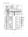
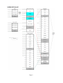
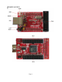
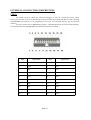
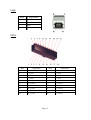
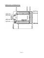
SAM3-H256 development board
Users Manual
All boards produced by Olimex are ROHS compliant
Rev. Initial, April 2011
Copyright(c) 2011, OLIMEX Ltd, All rights reserved
Page 1
INTRODUCTION:
Atmel’s ATSAM3S4BA-AU is a member of a series of Flash microcontrollers based on the high performance 32-bit ARM Cortex-M3 RISC processor. It operates at a maximum speed of 64 MHz and features a 256 Kbyte Flash and a 48 Kbyte
SRAM, Full Speed USB Device port with embedded transceiver, an External Bus
Interface featuring a Static Memory Controller providing connection to SRAM,
PSRAM, NOR Flash and NAND Flash, 2x USARTs, 2x UARTs, 2x TWIs, 3x SPI, an
I2S, as well as 1 PWM timer, 6x general-purpose 16-bit timers, an RTC, an ADC, a
12-bit DAC and an analog comparator.
SAM3-H256 has connectors for JTAG and USB, extension headers for all
microcontroller's ports, reset button, power and status leds.
BOARD FEATURES:
•
Microcontroller: ATSAM3S4BA-AU.
•
standard JTAG connector with ARM 2x10 pin layout for programming/debugging with ARM-JTAG
•
status LED
•
on board voltage regulator 3.3V with up to 800mA current
•
power supply LED
•
power supply filtering capacitor
•
RESET circuit
•
RESET button
•
12.000 Mhz crystal on socket
•
extension headers for all microcontroller's ports
•
PCB: FR-4, 1.5 mm (0,062"), soldermask, silkscreen component print
•
Dimensions: 50.00 x 33.75 mm (1.97 x 1.33")
ELECTROSTATIC WARNING:
The SAM3-H256 board is shipped in protective anti-static packaging. The board
must not be subject to high electrostatic potentials. General practice for working
with static sensitive devices should be applied when working with this board.
BOARD USE REQUIREMENTS:
Cables: The cable you will need depends on the programmer/debugger you use. If
you use ARM-JTAG-EW, you will need USB A-B cable.
Hardware:
Programmer/Debugger ARM-JTAG-EW or other compatible
programming/debugging tool if you work with EW-ARM.
Page 2
You can use also ARM-USB-OCD, ARM-USB-TINY, ARM-USB-OCD-H, ARMUSB-TINY-H.
PROCESSOR FEATURES:
SAM3-H256 board use ARM-based microcontroller ATSAM3S4BA-AU from
Atmel Corporation with these features:
−
Core
−
ARM® Cortex®-M3 revision 2.0 running at 64 MHz
−
Memory Protection Unit (MPU)
−
Thumb®-2 instruction set
−
Pin-to-pin compatible with AT91SAM7S legacy products (48- and 64-pin
versions)
−
Memories
−
−
−
256 Kbytes embedded Flash, 128-bit wide access, memory accelerator,
single plane
−
48 Kbytes embedded SRAM
−
16 Kbytes ROM with embedded bootloader routines (UART, USB) and
IAP routines
−
8-bit Static Memory Controller (SMC): SRAM, PSRAM, NOR and
NAND Flash support
−
Memory Protection Unit (MPU)
System
−
Embedded voltage regulator for single supply operation
−
Power-on-Reset (POR), Brown-out Detector (BOD) and Watchdog for
safe operation
−
Quartz or ceramic resonator oscillators: 3 to 20 MHz main power with
Failure Detection and optional low power 32.768 kHz for RTC or
device clock
−
High precision 8/12 MHz factory trimmed internal RC oscillator with
4 MHz default frequency for device startup. In-application trimming
access for frequency adjustment
−
Slow Clock Internal RC oscillator as permanent low-power mode
device clock
−
Two PLLs up to 130 MHz for device clock and for USB
−
Temperature Sensor
−
Up to 22 peripheral DMA (PDC) channels
Low Power Modes
−
Sleep and Backup modes, down to 3 μA in Backup mode
Page 3
−
−
−
Ultra low power RTC
Peripherals
−
USB 2.0 Device: 12 Mbps, 2668 byte FIFO, up to 8 bidirectional
Endpoints. On-Chip Transceiver
−
2 USARTs with ISO7816, IrDA®, RS-485, SPI, Manchester and Modem
Mode
−
Two 2-wire UARTs
−
2 Two Wire Interface (I2C compatible), 1 SPI, 1 Serial Synchronous
Controller (I2S), 1 High Speed Multimedia Card Interface (SDIO/SD
Card/MMC)
−
3 Three-Channel 16-bit Timer/Counter with capture, waveform,
compare and PWM mode. Quadrature Decoder Logic and 2-bit Gray
Up/Down Counter for Stepper Motor
−
4-channel 16-bit PWM with Complementary Output, Fault Input, 12bit Dead Time Generator Counter for Motor Control
−
32-bit Real-time Timer and RTC with calendar and alarm features
−
10-channel ADC with differential input mode and programmable gain
stage
−
Two 12-bit DAC outputs
−
One Analog Comparator with flexible input selection, Selectable input
hysteresis
−
32-bit Cyclic Redundancy Check Calculation Unit (CRCCU)
−
47 I/O lines with external interrupt capability (edge or level
sensitivity), debouncing, glitch filtering and on-die Series Resistor
Termination
−
Three 32-bit Parallel Input/Output Controllers, Peripheral DMA
assisted Parallel Capture Mode
I/O
Page 4
BLOCK DIAGRAM:
Page 5
MEMORY MAP:
Page 6
1N5819S/SMD
Page 7
USB
USB_B
G ND
C13
10n
NA(IRLML6402)
FET1
S H IE L D
1
2
3
4
33p
C8
R15
NA(1.5K)
R14
27R
R17
27R
15p
C14
PUP
R16
NA(100)
0
R11
R18
330K
0
R10
15p
C15
R7
47K
RST
R8
47K
OUT
R19
330K
TDO
TDI
TMS
TCK
R9
47K
R3
390/1%
R1
240/1%
2 VCC
C17
2.2uF
1n
C11
100n
100n
C18
3.3V
100n
C19
RESET
C9
100n
R12
10K
RST
VIN
3.3V
3.3V
R2
560
PWR
C16
C12
100n
C10
100n
C7
2.2uF
C5
100n
GND
RESET 1
U1
MCP130T
47uF/6.3V
C1
3
USB
100n
NA(47K)
R13
R6
47K
R5
47K
10uF/16V
C2
IN
ADJ/GND
3.3V
+
C3
D1
3.3V
JTAG
1
3 TRST
5
7
9
11 RTCK
13
15
17
19
3.3V
+
2
4
6
8
10
12
14
16
18
20
VIN
VR1(3.3V)
LM1117IMPX-ADJ
100n
C20
C6
10p
C4
10p
TEST
1x2
RST
100n
C21
Q1
12MHz/PTH
TCK
TDI
TDO
TMS
2
1
3.3V
EXT2-17
EXT2-18
EXT2-19
EXT2-20
L_E
1x2
2
1
STAT
8
PB13
PB14
PB12
R4
560
3.3V
2
17
46
60
12
24
54
64
8
18
45
58
59
7
61
62
63
56
57
50
53
33
49
51
40
39
55
ATSAM3S4BA-AU
PA0/PWMH0/TIOA0/A17/WKUP0
PA1/PWMH1/TIOB0/A18/WKUP1
PA2/PWMH2/SCK0/DATRG/WKUP2
PA3/TWD0/NPCS3
JTAGSEL
PA4/TWCK0/TCLK0/WKUP3
PB7/TCK/SWCLK
PA5/RXD0/NPCS3/WKUP4
PB4/TWD1/PWMH2/TDI
PA6/TXD0/PCK0
PB5/TWCK1/PWML0/WKUP13/TDO/TRACESWO
PA7/RTS0/PWMH3/XIN32
PB6/TMS/SWDIO
PA8/CTS0/ADTRG/WKUP5/XOUT32
PA9/URXD0/NPCS1/PWMFI0/WKUP6
PB10/DDM
PA10/UTXD0/NPCS2
PB11/DDP
PA11/NPCS0/PWMH0/WKUP7
PA12/MISO/PWMH1
PB14/NPCS1/PWMH3/DAC1
PA13/MOSI/PWMH2
PA14/SPCK/PWMH3/WKUP8
PB9/XIN
PA15/TF/TIOA1/PWML3/WKUP14/PIODCEN1
PA16/TK/TIOB1/PWML2/WKUP15/PIODCEN2
PB8/XOUT
PA17/TD/PCK1/PWMH3/AD0
PA18/RD/PCK2/A14/AD1
VDDIN
PA19/RK/PWML0/A15/AD2/WKUP9
PA20/RF/PWML1/A16/AD3/WKUP10
PB13/PWML2/PCK0/DAC0
PA21/RXD1/PCK1/AD8
PA22/TXD1/NPCS3/NCS2/AD9
VDDIO1
PA23/SCK1/PWMH0/A19/PIODCCLK
VDDIO2
PA24/RTS1/PWMH1/A20/PIODC0
VDDIO3
PA25/CTS1/PWMH2/A23/PIODC1
PA26/DCD1/TIOA2/MCDA2/PIODC2
VDDOUT
PA27/DTR1/TIOB2/MCDA3/PIODC3
PA28/DSR1/TCLK1/MCCDA/PIODC4
VDDPLL
PA29/RI1/TCLK2/MCCK/PIODC5
PA30/PWML2/NPCS2/MCDA0/WKUP11/PIODC6
VDDCORE1
PA31/NPCS1/PCK2/MCDA1/PIODC7
VDDCORE2
VDDCORE3
ADVREF
GND1
PB0/PWMH0/AD4
GND2
PB1/PWMH1/AD5
GND3
PB2/URXD1/NPCS2/WKUP12/AD6
GND4
PB3/UTXD1/PCK2/AD7
TST
NRST
PB12/PWML1/ERASE
U2
http://www.olimex.com/dev
CO PYRIGHT(C) 2011, O LIMEX Ltd.
Rev. Initial
SAM3-H256
1
3
4
5
6
48
47
44
43
36
35
34
32
31
30
29
28
27
22
21
20
19
9
10
13
16
11
14
15
23
25
26
37
38
41
42
52
PUP
AR
A4
A5
A6
A7
17
18
19
20
21
22
23
24
25
26
27
28
29
30
31
8
9
10
11
12
13
14
15
0
1
2
3
4
5
6
7
EXT2-13
EXT2-14
EXT2-15
EXT2-16
PB3
EXT1-1
EXT1-2
EXT1-3
EXT1-4
EXT1-5
EXT1-6
EXT1-7
EXT1-8
EXT1-9
EXT1-10
EXT1-11
EXT1-12
EXT1-13
EXT1-14
EXT1-15
EXT1-16
EXT1-17
EXT1-18
EXT1-19
EXT1-20
EXT2-1
EXT2-2
EXT2-3
EXT2-4
EXT2-5
EXT2-6
EXT2-7
EXT2-8
EXT2-9
EXT2-10
EXT2-11
EXT2-12
SCHEMATIC:
BOARD LAYOUT:
Page 8
POWER SUPPLY CIRCUIT:
SAM3-H256 is typically power supplied with +5 V from USB, but it also can be
power supplied with +5VDC via extension connector (signal VIN from EXT2
connector pin17).
The programmed board power consumption is about 50 mA.
RESET CIRCUIT:
SAM3-H256 reset circuit includes U1 (MCP130T), R12 (10k), JTAG
connector pin 15, EXT2 pin 20, ATSAM3S4BA-AU pin 39 (NRST) and RESET
button.
CLOCK CIRCUIT:
Quartz crystal Q1 12.000 MHz is connected to ATSAM3S4BA-AU pin 61
(PB8/XOUT) and pin 62 (PB9/XIN).
JUMPER DESCRIPTION:
L_E
This jumper, when closed, enables status led – STAT.
Default state is closed.
TEST
This jumper, when closed, connects ATSAM3S4BA-AU pin 40 (TST) to 3.3V. The TST
pin is used for JTAG Boundary Scan Manufacturing Test or Fast Flash programming
mode.
When TEST jumper is opened – normal mode is enabled.
Default state is opened.
Page 9
Description for programming via USB port using SAM-BA software
The ATSAM3S4BA-AU can be programmed via USB using the SAM-BATM software. Before
being able to use SAM-BA, a recovery procedure, which consists of copying the SAM-BA Boot
Assistant into Flash must be performed as follows:
1. Disconnect board from USB
2. Connect PB12 to 3.3V
3. Power up the board
4. Wait 10s
5. Power down the board
6. Remove the connection between PB12 and 3.3V
7. Power up the board via USB
8. If SAM-BA USB driver are installed you can use SAM-BA tool
INPUT/OUTPUT:
Status Led (green) with name STAT connected via jumper L_E to ATSAM3S4BAAU pin 31 (PA8/CTS0/ADTRG/WKUP5/XOUT32).
Power-on LED (red) with name PWR – this LED shows that +3.3V is applied to the
board.
Reset button with name RESET connected to ATSAM3S4BA-AU pin 39 (NRST).
Page 10
EXTERNAL CONNECTORS DESCRIPTION:
JTAG:
The JTAG connector allows the software debugger to talk via a JTAG (Joint Test Action
Group) port directly to the core. Instructions may be inserted and executed by the core thus allowing
ATSAM3S4BA-AU memory to be programmed with code and executed step by step by the host
software.
For more details refer to IEEE Standard 1149.1 - 1990 Standard Test Access Port and Boundary
Scan Architecture and ATSAM3S4BA-AU datasheets and users manual.
Pin #
Signal Name
Pin #
Signal Name
1
3.3V
2
3.3V
3
TRST
4
GND
5
TDI
6
GND
7
TMS
8
GND
9
TCK
10
GND
11
RTCK
12
GND
13
TDO
14
GND
15
RST
16
GND
17
NC
18
GND
19
NC
20
GND
Page 11
USB:
Pin #
Signal Name
1
VIN
2
DDM
3
DDP
4
GND
EXT1:
Pin #
Signal Name
Pin #
Signal Name
1
0 - (PA0)
2
1 - (PA1)
3
2 – (PA2)
4
3 – (PA3)
5
4 – (PA4)
6
5 – (PA5)
7
6 – (PA6)
8
7 – (PA7)
9
8 - (PA8)
10
9 – (PA9)
11
10 – (PA10)
12
11 – (PA11)
13
12 – (PA12)
14
13 – (PA13)
15
14 – (PA14)
16
15 – (PA15)
17
PUP – (PA16)
18
17 – (PA17)
19
18 – (PA18)
20
19 – (PA19)
Page 12
EXT2:
Pin #
Signal Name
Pin #
Signal Name
1
20 – (PA20)
2
21 – (PA21)
3
22 – (PA22)
4
23 – (PA23)
5
24 – (PA24)
6
25 – (PA25)
7
26 – (PA26)
8
27 – (PA27)
9
28 – (PA28)
10
29 – (PA29)
11
30 – (PA30)
12
31 – (PA31)
13
AR – (ADVREF)
14
A4 – (PB0)
15
A5 – (PB1)
16
A6 - (PB2)
17
VIN
18
VCC
19
GND
20
RST
Page 13
MECHANICAL DIMENSIONS:
Page 14
AVAILABLE DEMO SOFTWARE:
Demonstrates USB mouse and a blinking led.
You can find it at http://www.olimex.com/dev at the board's specific page.
Page 15
ORDER CODE:
SAM3-H256 - assembled and tested board
How to order?
You can order to us directly or by any of our distributors.
Check our web www.olimex.com/dev for more info.
Revision history:
Board's Revision:
Initial, October 2010
Manual's Revision
Initial, April 2011
Page 16
Disclaimer:
© 2011 Olimex Ltd. All rights reserved. Olimex®, logo and combinations thereof, are registered
trademarks of Olimex Ltd. Other terms and product names may be trademarks of others.
The information in this document is provided in connection with Olimex products. No license, express
or implied or otherwise, to any intellectual property right is granted by this document or in
connection with the sale of Olimex products.
Neither the whole nor any part of the information contained in or the product described in this
document may be adapted or reproduced in any material from except with the prior written
permission of the copyright holder.
The product described in this document is subject to continuous development and improvements. All
particulars of the product and its use contained in this document are given by OLIMEX in good faith.
However all warranties implied or expressed including but not limited to implied warranties of
merchantability or fitness for purpose are excluded.
This document is intended only to assist the reader in the use of the product. OLIMEX Ltd. shall not
be liable for any loss or damage arising from the use of any information in this document or any error
or omission in such information or any incorrect use of the product.
Page 17