1
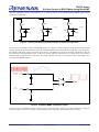
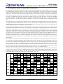
To our customers,
Old Company Name in Catalogs and Other Documents
On April 1st, 2010, NEC Electronics Corporation merged with Renesas Technology
Corporation, and Renesas Electronics Corporation took over all the business of both
companies. Therefore, although the old company name remains in this document, it is a valid
Renesas Electronics document. We appreciate your understanding.
Renesas Electronics website: http://www.renesas.com
April 1st, 2010
Renesas Electronics Corporation
Issued by: Renesas Electronics Corporation (http://www.renesas.com)
Send any inquiries to http://www.renesas.com/inquiry.
Notice
1.
2.
3.
4.
5.
6.
7.
All information included in this document is current as of the date this document is issued. Such information, however, is
subject to change without any prior notice. Before purchasing or using any Renesas Electronics products listed herein, please
confirm the latest product information with a Renesas Electronics sales office. Also, please pay regular and careful attention to
additional and different information to be disclosed by Renesas Electronics such as that disclosed through our website.
Renesas Electronics does not assume any liability for infringement of patents, copyrights, or other intellectual property rights
of third parties by or arising from the use of Renesas Electronics products or technical information described in this document.
No license, express, implied or otherwise, is granted hereby under any patents, copyrights or other intellectual property rights
of Renesas Electronics or others.
You should not alter, modify, copy, or otherwise misappropriate any Renesas Electronics product, whether in whole or in part.
Descriptions of circuits, software and other related information in this document are provided only to illustrate the operation of
semiconductor products and application examples. You are fully responsible for the incorporation of these circuits, software,
and information in the design of your equipment. Renesas Electronics assumes no responsibility for any losses incurred by
you or third parties arising from the use of these circuits, software, or information.
When exporting the products or technology described in this document, you should comply with the applicable export control
laws and regulations and follow the procedures required by such laws and regulations. You should not use Renesas
Electronics products or the technology described in this document for any purpose relating to military applications or use by
the military, including but not limited to the development of weapons of mass destruction. Renesas Electronics products and
technology may not be used for or incorporated into any products or systems whose manufacture, use, or sale is prohibited
under any applicable domestic or foreign laws or regulations.
Renesas Electronics has used reasonable care in preparing the information included in this document, but Renesas Electronics
does not warrant that such information is error free. Renesas Electronics assumes no liability whatsoever for any damages
incurred by you resulting from errors in or omissions from the information included herein.
Renesas Electronics products are classified according to the following three quality grades: “Standard”, “High Quality”, and
“Specific”. The recommended applications for each Renesas Electronics product depends on the product’s quality grade, as
indicated below. You must check the quality grade of each Renesas Electronics product before using it in a particular
application. You may not use any Renesas Electronics product for any application categorized as “Specific” without the prior
written consent of Renesas Electronics. Further, you may not use any Renesas Electronics product for any application for
which it is not intended without the prior written consent of Renesas Electronics. Renesas Electronics shall not be in any way
liable for any damages or losses incurred by you or third parties arising from the use of any Renesas Electronics product for an
application categorized as “Specific” or for which the product is not intended where you have failed to obtain the prior written
consent of Renesas Electronics. The quality grade of each Renesas Electronics product is “Standard” unless otherwise
expressly specified in a Renesas Electronics data sheets or data books, etc.
“Standard”:
8.
9.
10.
11.
12.
Computers; office equipment; communications equipment; test and measurement equipment; audio and visual
equipment; home electronic appliances; machine tools; personal electronic equipment; and industrial robots.
“High Quality”: Transportation equipment (automobiles, trains, ships, etc.); traffic control systems; anti-disaster systems; anticrime systems; safety equipment; and medical equipment not specifically designed for life support.
“Specific”:
Aircraft; aerospace equipment; submersible repeaters; nuclear reactor control systems; medical equipment or
systems for life support (e.g. artificial life support devices or systems), surgical implantations, or healthcare
intervention (e.g. excision, etc.), and any other applications or purposes that pose a direct threat to human life.
You should use the Renesas Electronics products described in this document within the range specified by Renesas Electronics,
especially with respect to the maximum rating, operating supply voltage range, movement power voltage range, heat radiation
characteristics, installation and other product characteristics. Renesas Electronics shall have no liability for malfunctions or
damages arising out of the use of Renesas Electronics products beyond such specified ranges.
Although Renesas Electronics endeavors to improve the quality and reliability of its products, semiconductor products have
specific characteristics such as the occurrence of failure at a certain rate and malfunctions under certain use conditions. Further,
Renesas Electronics products are not subject to radiation resistance design. Please be sure to implement safety measures to
guard them against the possibility of physical injury, and injury or damage caused by fire in the event of the failure of a
Renesas Electronics product, such as safety design for hardware and software including but not limited to redundancy, fire
control and malfunction prevention, appropriate treatment for aging degradation or any other appropriate measures. Because
the evaluation of microcomputer software alone is very difficult, please evaluate the safety of the final products or system
manufactured by you.
Please contact a Renesas Electronics sales office for details as to environmental matters such as the environmental
compatibility of each Renesas Electronics product. Please use Renesas Electronics products in compliance with all applicable
laws and regulations that regulate the inclusion or use of controlled substances, including without limitation, the EU RoHS
Directive. Renesas Electronics assumes no liability for damages or losses occurring as a result of your noncompliance with
applicable laws and regulations.
This document may not be reproduced or duplicated, in any form, in whole or in part, without prior written consent of Renesas
Electronics.
Please contact a Renesas Electronics sales office if you have any questions regarding the information contained in this
document or Renesas Electronics products, or if you have any other inquiries.
(Note 1) “Renesas Electronics” as used in this document means Renesas Electronics Corporation and also includes its majorityowned subsidiaries.
(Note 2) “Renesas Electronics product(s)” means any product developed or manufactured by or for Renesas Electronics.
APPLICATION NOTE
R8C/25 Group
Six Step Trapezoidal Control of a BLDC Motor Using Back-EMF
Introduction
This document describes a method of commutating a 3-Phase Brushless DC (BLDC) motor using Back-EMF (BEMF)
signals.
This document is intended to supplement the understanding of 6-step BLDC motor control using BEMF detection as
one of many possible methods of commutation. The BEMF-detection method, as well as the Hall device method, are
implemented on the Renesas YMCRPR8C25 Motor Control Evaluation kit, which provides an excellent platform for
developing the algorithm for individual applications.
The reader should already have some understanding of six-step commutation methods, such as Hall commutation, to
provide background to the techniques described here. The reader is encouraged to first read the 6-Step Motor Drive
with HALL sensor Application Note referred to in the Reference section at the end of this document.
Target Devices
R8C/24 and R8C/25
Contents
1.
Motor Back-EMF Signal Characteristics ........................................................................................... 2
2.
Detecting Back-EMF Signals for Commutation................................................................................. 3
3.
Driving BLDC Motor for Back-EMF Commutation............................................................................. 5
4.
Open-Loop Alignment and Rotation Starting .................................................................................... 6
5.
How to deal with Inductive Effects .................................................................................................... 7
6.
Summary ........................................................................................................................................... 8
7.
Reference.......................................................................................................................................... 9
REU05B0073-0101/Rev.1.01
February 2009
Page 1 of 10
R8C/25 Group
Six Step Control of BLDC Motor Using Back-EMF
1.
Motor Back-EMF Signal Characteristics
A 3-phase Permanent Magnet Brushless DC (PM-BLDC) motor generates 3-phase AC voltages (shown in Figure 1)
called a Back Electro-Motive Force (also Back-EMF or BEMF) as it rotates. The amplitude and frequency of the
generated voltage are proportional to the rotational speed. If the motor has a single pole pair on the rotor (one North
and one South pole) then the Frequency of the BEMF voltage will be the same as the rotational speed of the rotor. If,
however, it has multiple magnetic poles (as motors often do), then the frequency will be will be higher, in proportion to
the number of pole pairs on the rotor. The voltage generated will be determined by the number of turns in the windings
and the strength of the rotor magnet. There will be a relationship then that can be established with the motor where it
will generate a particular AC voltage when it is spinning at a particular speed. This value can be expressed as a
constant Ke, it equals the volts generated at some RPM, usually 1000 RPM. Motor manufacturers usually provide the
value of this constant.
Speed
Phase-to-phase Voltage (BEMF)
Figure 1 Voltage and frequency measured externally at rotating BLDC motor
In most BLDC motors, we normally only have access to the three windings, not to the center tap (neutral), so the
voltages have to be seen between two phases where it is the difference of the voltages between those windings. If one
voltage is near maximum, and the other is near minimum, then the voltage seen between them will be larger than if the
two phases were both positive or were both negative, relative to the neutral. For the purpose of commutation with the
BEMF signals, we want to know when a phase voltage crosses zero with respect to the neutral. As it happens, when
one phase is crossing neutral, the other two phases are at equal and opposite voltages, so we can detect a zero crossing
of one phase when its measured voltage is exactly between the other two. For purposes of this document, we will
assume that BLDC motors are always constructed symmetrically, with similar BEMF, resistance and inductance in all
three phases.
REU05B0073-0101/Rev.1.01
February 2009
Page 2 of 10
R8C/25 Group
Six Step Control of BLDC Motor Using Back-EMF
Figure 2 Rotating vector representation of motor phases
2.
Detecting Back-EMF Signals for Commutation
The voltage present on the motor phases is a combination of those generated internally and of those being driven
externally by our transistors with PWM voltages. So, detecting BEMF on an undriven motor is easy, but not so when
we are also trying to force current into the windings to generate torque and cause it to spin. The internal voltages are
due to the BEMF and to affects from the resistance and inductance of the motor which are functions of the current
flowing in the windings. The PWM voltages that we use to drive the motor windings externally will likely be much
higher than the BEMF voltages we are trying to detect. Despite this, we need some way of seeing the BEMF voltage
near the time when the phase crosses zero, so we can decide when to commutate. In order to get a clean representation
of the BEMF voltage, it is necessary to filter the high frequency PWM signals from the motor phase voltage, leaving
only the lower frequency BEMF signal. After that, we can also deal with the voltages due to the resistive and inductive
effects.
For example, if we use a common PWM carrier frequency of 12 kHz, the BEMF frequency will likely be much lower,
around a few hundred Hz. The exact value of the BEMF frequency can be found as BEMF_Hz = RPM x (1 min/60 sec)
x Number_of_Pole_Pairs. So, for a motor with 5 pole pairs, running at 3000 RPM, the BEMF frequency is 250 Hz.
The difference between 12 kHz and 250 Hz allows us some room to create a low-pass filter that will pass the BEMF
component, while attenuating the PWM component.
Figure 3 Raw and filtered motor voltage
Assuming the bus voltage is higher than the logic-level voltages, then the motor voltage should be also divided down to
scale it to those that can be observed by the comparator logic. The circuits used to scale down and filter the motor
phases voltages are shown below in Figure 4. The U, V and W are the motor lines, with PWM and BEMF components
REU05B0073-0101/Rev.1.01
February 2009
Page 3 of 10
R8C/25 Group
Six Step Control of BLDC Motor Using Back-EMF
up to 50V (divided by a factor of 10) and the V_U, V_V and V_W lines are the scaled and filtered BEMF signals which
are fed into comparators.
W
V
U
90.9k
90.9k
90.9 k
10k
10k
0.015uF
V_W
V_V
V_U
10k
0.015uF
0.015 uF
Figure 4 Filtering and Scaling of phase voltages to match the logic levels
Once we have the BEMF voltages filtered and scaled, we compare it with a reference point, derived from the bus
voltage. We do this because the motor phases are modulated from the bus, and if the bus voltage varies by any amount,
the reference and phase voltage will remain proportional. One difference from the motor filter and divider is that the
bus reference is scaled at half the value. In this way, the bus reference will always be at a point where we can detect
when the phase voltage is above or below the 50% value, which we will see, is a convenient way for detecting the zero
crossing in the BEMF voltages.
MOTOR PHASE
VOLTAGE
BUS
VOLTAGE
Figure 5 Simplified BEMF comparator signals
The next step is to modulate the motor in such a way as to keep the motor neutral very close to half the bus voltage so
that when a phase does a zero crossing, it can be detected by the comparator at the half-bus reference point.
REU05B0073-0101/Rev.1.01
February 2009
Page 4 of 10
R8C/25 Group
Six Step Control of BLDC Motor Using Back-EMF
3.
Driving BLDC Motor for Back-EMF Commutation
For complementary PWM, each comparator register in the PWM timer produces two PWM outputs, not just one. The
two complementary signals are used in one phase of the three phase PWM, so there are a total of three comparator
registers and six PWM outputs or three pairs. One of each pair is designated as the upper transistor driver, and the other
is the lower. We use the convention that as the PWM compare value increases, the upper transistor duty for that phase
becomes larger, and the lower duty becomes smaller. The two signals are complementary in that they are the logical
inversion, or complement, of the other, so that the two signals are not active at the same time. In reality, the TimerRD
also allows “deadtime” settings, which introduces a period of time when both pulses are inactive, to allow for switching
time in the transistors. See the R8C/25 hardware manual for more detail on TimerRD used in Complementary PWM
mode.
As mentioned above, we need to apply voltages which are centered about the middle of the bus in order to allow zerocrossings to be detected at the half-bus reference. We can do this type of voltage driving to the motor phases using
voltages symmetric about the half-bus level. We use complementary PWM and a reference level of 50% PWM duty for
both the higher and lower side voltages on two of the phases.
We set up the PWM output near a value of 50% for both driven phases, but increase one phase duty by some amount
and lower the other phase the same amount. For example, if we drive phase U to 60% duty, then we can drive phase V
at 40% duty, the difference is 20%, as will be seen by the motor phases, and the middle of the two will still be 50%,
where we are detecting the zero-crossing on phase W. A look at the voltage present at phase W will still have the PWM
components of the other two phases, but once filtered, the PWM components of phases U and V will be removed,
leaving the correct representation of the phase W voltage. When the phase W signal crosses the middle of the bus, it is
also the same angle where phase U and V are equal and opposite and also balanced around the middle of the bus, so our
assumption of symmetry allows us to detect that phase W has crossed zero without measuring the neutral point directly.
Voltage drops caused by the resistance in the other phases are cancelled, since the current through the other phases must
also be equal.
In the software, this method of symmetrical modulation is easy to implement. For any given duty desired, we normalize
it to the range of 50% duty, then add or subtract that value from a set value of 50% for two of the phases. So, if we
have 1024 counts of PWM total (meaning that a value of 1024 will give us 100% duty PWM on the upper channel and
0% on the lower), then 50% (for both upper and lower, in complement) will be a timer compare value 512. For a motor
needing apparent 50% duty, we actually add 25% to 50% for one phase and subtract 25% from 50% for the other,
creating a total of 50%, but each only 25% offset from the 50% reference. We can now guarantee that the motor neutral
will be very near the center of the bus when the undriven phase crosses zero on its BEMF output.
Of course, only two of the phases are being driven at one time, the floating phase is the one being observed for BEMF
crossing. Once a decision is made to commutate and switch the transistors, the floating phase should be the one next
approaching the zero crossing. We use the data from the present commutation state (or Step), along with the zero
crossing detection to continue moving the motor to the next Step, and so on.
Figure 6 Simulated PWM signals
REU05B0073-0101/Rev.1.01
February 2009
Page 5 of 10
R8C/25 Group
Six Step Control of BLDC Motor Using Back-EMF
Since the BEMF detection is done by observing the phase voltage, which is a function of speed and of the driving
voltage of our PWM, it is necessary to get the motor running at some speed before the BEMF voltage is large enough to
be detected. So, for starting the motor from full stop, where no BEMF voltage exists, we have to force the motor to spin
first before we can use BEMF detection to continue the commutation. For that, we use open-loop alignment and startup techniques.
4.
Open-Loop Alignment and Rotation Starting
The method of commutating by detecting BEMF voltages requires that the motor is already spinning and generating a
reasonable amplitude BEMF signal before commutation can be done.
To make that happen, we first force the rotor into a known position in an alignment process. This can be done by
setting the voltage on Phase U higher than V and W. That is done by setting PWM counts for U higher and the counts
in V and W smaller. Though alignment can be done with only two phases, by applying the same voltage to two of the
phases produces a natural damping effect to help the motor settle more quickly into the alignment position.
Figure 7 Concept of alignment current
We slowly increase this voltage (that is, the PWM duty), to not impart an impulse to the motor, which may cause it to
oscillate. We do this process for up to several seconds, to allow the rotor to align with the currents, and to allow any
spontaneous rotational oscillation to dampen out. Small motors with low inertia may align in less than a second, while
large inertia loads require more time.
Once we are sure the motor is in a known alignment state, we begin sending a slowly accelerating stepped current into
the motor phases to get the motor to spin in the desired direction. We commutate as in Figure 6 above, increasing and
cycling through the Step count as we go. The initial duty cycle is selected to overcome the frictional forces and inertia
of the motor. We increase the voltage sent to the phases as well as increase the step rate to force the motor to turn and
accelerate, overcoming the motor friction, inertia and the increasing back-EMF. Because there is no commutation
feedback during this stage to keep the currents aligned with the rotor, the open-loop currents must be larger than normal
to maintain the torque. It is important, therefore, to set the alignment voltage and time, as well as the ramp rate and
voltage to match the motor and load to ensure a reliable start.
REU05B0073-0101/Rev.1.01
February 2009
Page 6 of 10
R8C/25 Group
Six Step Control of BLDC Motor Using Back-EMF
The software should increase the open-loop commutation switch rate until such time that the BEMF is large enough to
generate reliable signals into the comparators. That rotational speed can be found by examining the BEMF signals
during hall commutation (if available) or empirically by selecting arbitrary speeds and checking results. Once the
motor has accelerated in the open-loop to our switch point, it is just a matter of changing over to the BEMF modulation
method, where the comparator output state determines the motor phase drive. Once BEMF commutation kicks in, the
motor current can be reduced since the voltage fed will now align with the motor BEMF signal, increasing the torque.
It is now possible to increase the ramp of applied voltage and accelerate the motor at a higher rate to the speed desired.
Figure 8 shows a waveform of this as the motor begins with alignment current, accelerates with open-loop current, then
when switched to BEMF commutation, the current required goes down significantly.
Figure 8 Speed and current waveforms
5.
How to deal with Inductive Effects
Commutating a BLDC motor (where the windings always have some inductance) means that there will be inductive
effects from changes in current on the voltage waveforms. The nature of inductance is to resist changes in current, and
larger changes in current require large voltage to be applied. Likewise, when current is forced to change during the
switching action of the transistors, large voltages can occur spontaneously in the windings, often called “inductive kick”.
When a phase is switched to float, the remaining current will decay, during which time the inductive kick will force the
voltage of a floating phase to discharge to one of the power rails (through diodes parallel with the transistors). The
length of time that this current discharge happens is proportional to the amount of current to be dissipated, and inversely
to the difference in voltage between the phase BEMF and the power rail.
Under low current conditions, the voltage pulse generated by the inductive kick is short in duration. Under larger
current, as when the motor load is larger, the time for the voltage to decay is longer. It is important to note that this
time must not be so long as to prevent the detection of the normal zero-crossing of the undriven phase, or BEMF
commutation is not possible. Assuming the current discharge time is short enough, then a masking interval can be used
to ignore the pulse at the output of the comparator. Selecting the right masking time is critical since if masking time is
REU05B0073-0101/Rev.1.01
February 2009
Page 7 of 10
R8C/25 Group
Six Step Control of BLDC Motor Using Back-EMF
too short, invalid commutation signals will cause currents to be switched to the wrong phase and decrease motor
efficiency. If the masking time is too long, the commutation rate is limited therefore the motor speed will be limited.
We use a timer in the software to mask the voltage pulses. This count is defined in software as a count on the PWM
timer and can be changed for different motors and load conditions. Once the masking time interval has passed, we
begin looking at the comparator output for a change which would indicate a valid change in step. Once that is detected,
we begin the timer again to mask the next voltage pulse for the same period of time.
Valid
edges
Figure 9 Filtered Back EMF and comparator output
Figure 9 shows a graph showing the comparator output, including the voltage pulse to be masked. The blue trace
(bottom) is the filtered BEMF, and the red trace (top) is the comparator output with extra edges. The first edge is the
valid one, the next two or three quickly following are the invalid edges, caused by the inductive pulse.
If we imagine the same comparator signals, but without the extra edges caused by the inductance, then what we find is
that the three comparator signals are nearly identical to what we would expect from Hall device signals. So, we can use
the comparator signals in much the same way we would with Hall signals, and use their state to determine the
commutation state. This is exactly what we do in the sample motor code supplied with the YMCRPR8C25 kit. The
BEMF code uses the three comparator edges, filters out the unwanted edges, and uses their state in a lookup table to
decide which transistors are switched to high, low, or float.
6.
Summary
In this application note we described a method of commutating a 3-Phase Brushless DC (BLDC) motor using BackEMF (BEMF) signals. The Renesas YMCRPR8C25 Motor Control kit is an excellent vehicle for evaluating BEMF
control using the R8C/Tiny Microcontroller devices. Offering a rich set of Motor Control peripherals, the R8C25
series is specifically suited for 3-phase motor control, including the BEMF method described here, as well as Hall-based
commutation and AC Induction motor control.
REU05B0073-0101/Rev.1.01
February 2009
Page 8 of 10
R8C/25 Group
Six Step Control of BLDC Motor Using Back-EMF
7.
Reference
YMCRPR8C25 Kit
User Manual
Application Notes
REU05B0074-0100/Rev 1.00
REJ05B0845-0100/Rev.1.00
REJ05B0486-0100Z/Rev.1.00
Six-Step Trapezoidal Control of a BLDC Motor Using Hall Sensors
Timer RD in Complementary PWM Mode
Solutions for Three-Phase Motor Control Programming
Hardware Manual
R8C/24 Group, R8C/25 Group Hardware Manual Rev. 1.0
YMCRPR8C25 Motor Control Demo Kit
(Use the latest version on the home page: http://www.renesas.com)
Website and Support
Renesas Technology Website
http://www.renesas.com/
Technical Contact Details:
Global: [email protected]
Inquiries
http://www.renesas.com/inquiry
Revision Record
Rev.
1.00
1.01
Date
Feb.05.08
Feb.02.09
REU05B0073-0101/Rev.1.01
Description
Page
Summary
—
First edition issued
10
Disclaimer changed
February 2009
Page 9 of 10
R8C/25 Group
Six Step Control of BLDC Motor Using Back-EMF
Notes regarding these materials
1.
2.
3.
4.
5.
6.
7.
8.
9.
10.
11.
12.
13.
This document is provided for reference purposes only so that Renesas customers may select the appropriate
Renesas products for their use. Renesas neither makes warranties or representations with respect to the
accuracy or completeness of the information contained in this document nor grants any license to any intellectual
property rights or any other rights of Renesas or any third party with respect to the information in this document.
Renesas shall have no liability for damages or infringement of any intellectual property or other rights arising out
of the use of any information in this document, including, but not limited to, product data, diagrams, charts,
programs, algorithms, and application circuit examples.
You should not use the products or the technology described in this document for the purpose of military
applications such as the development of weapons of mass destruction or for the purpose of any other military
use. When exporting the products or technology described herein, you should follow the applicable export
control laws and regulations, and procedures required by such laws and regulations.
All information included in this document such as product data, diagrams, charts, programs, algorithms, and
application circuit examples, is current as of the date this document is issued. Such information, however, is
subject to change without any prior notice. Before purchasing or using any Renesas products listed in this
document, please confirm the latest product information with a Renesas sales office. Also, please pay regular
and careful attention to additional and different information to be disclosed by Renesas such as that disclosed
through our website. (http://www.renesas.com)
Renesas has used reasonable care in compiling the information included in this document, but Renesas
assumes no liability whatsoever for any damages incurred as a result of errors or omissions in the information
included in this document.
When using or otherwise relying on the information in this document, you should evaluate the information in light
of the total system before deciding about the applicability of such information to the intended application.
Renesas makes no representations, warranties or guaranties regarding the suitability of its products for any
particular application and specifically disclaims any liability arising out of the application and use of the
information in this document or Renesas products.
With the exception of products specified by Renesas as suitable for automobile applications, Renesas products
are not designed, manufactured or tested for applications or otherwise in systems the failure or malfunction of
which may cause a direct threat to human life or create a risk of human injury or which require especially high
quality and reliability such as safety systems, or equipment or systems for transportation and traffic, healthcare,
combustion control, aerospace and aeronautics, nuclear power, or undersea communication transmission. If you
are considering the use of our products for such purposes, please contact a Renesas sales office beforehand.
Renesas shall have no liability for damages arising out of the uses set forth above.
Notwithstanding the preceding paragraph, you should not use Renesas products for the purposes listed below:
(1) artificial life support devices or systems
(2) surgical implantations
(3) healthcare intervention (e.g., excision, administration of medication, etc.)
(4) any other purposes that pose a direct threat to human life
Renesas shall have no liability for damages arising out of the uses set forth in the above and purchasers who
elect to use Renesas products in any of the foregoing applications shall indemnify and hold harmless Renesas
Technology Corp., its affiliated companies and their officers, directors, and employees against any and all
damages arising out of such applications.
You should use the products described herein within the range specified by Renesas, especially with respect to
the maximum rating, operating supply voltage range, movement power voltage range, heat radiation
characteristics, installation and other product characteristics. Renesas shall have no liability for malfunctions or
damages arising out of the use of Renesas products beyond such specified ranges.
Although Renesas endeavors to improve the quality and reliability of its products, IC products have specific
characteristics such as the occurrence of failure at a certain rate and malfunctions under certain use conditions.
Please be sure to implement safety measures to guard against the possibility of physical injury, and injury or
damage caused by fire in the event of the failure of a Renesas product, such as safety design for hardware and
software including but not limited to redundancy, fire control and malfunction prevention, appropriate treatment
for aging degradation or any other applicable measures. Among others, since the evaluation of microcomputer
software alone is very difficult, please evaluate the safety of the final products or system manufactured by you.
In case Renesas products listed in this document are detached from the products to which the Renesas products
are attached or affixed, the risk of accident such as swallowing by infants and small children is very high. You
should implement safety measures so that Renesas products may not be easily detached from your products.
Renesas shall have no liability for damages arising out of such detachment.
This document may not be reproduced or duplicated, in any form, in whole or in part, without prior written
approval from Renesas.
Please contact a Renesas sales office if you have any questions regarding the information contained in this
document, Renesas semiconductor products, or if you have any other inquiries.
© 2008. Renesas Technology Corp., All rights reserved.
REU05B0073-0101/Rev.1.01
February 2009
Page 10 of 10