1
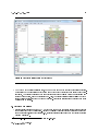
OpenStax-CNX module: m42302
1
A Quartus Project from Start to
∗
Finish: 2 Bit Mux Tutorial
Chris Stevenson
Joseph Cavallaro
Matthew Johnson
This work is produced by OpenStax-CNX and licensed under the
Creative Commons Attribution License 3.0†
Abstract
Describes the creation of a project using Altera's Quartus II 11.0, simulating with the Altera University Program Simulator, and programming the DE0 board from Terasic.
1 Building Projects in Quartus
This section is intended to provide an in-depth introduction to creating projects in Quartus, laying out
a circuit diagram, simulating the circuit, and nally using the project to congure an FPGA through an
example project showcasing a 2-bit MUX. Altera has made a very nice tutorial for Quartus as well which
1
you can nd here
. Altera's tutorial is meant for a dierent board than the DE0 we will be using so make
sure to account for that. Also, they have a slightly dierent method for connecting inputs and outputs to
the FPGA. Either method works and you can use whichever one you prefer, however, the method set forth
in this section will likely be more straightforward and user-friendly. Additionally, you can access another
tutorial from within Quartus at any time by clicking on Tutorial in the Help menu.
1.1 Starting a Quartus Project
A Quartus project acts as a support structure for a collection of design les. It serves to bring them together
in a common working environment, dene their relationships both within the project to each other and to
the FPGA, and dene common characteristics. All work in Quartus starts with a project.
•
Begin by opening Quartus II Web Edition. A screen titled Getting Started with Quartus II Software
should open from which you can select Create a New Project.
Otherwise select File->New Project
Wizard. Make sure you select this and not simply New, which would instead create a new le.
•
In the working directory eld specify the folder,My_Quartus_Projects for the purpose of this example, to save your project in. While you can make this folder on your U: drive, Quartus will generally
run faster if working on projects in the C: drive. It is recommended to make temporary folder on the
C: drive to put your projects in and transfer them to your U: drive for safe keeping. Note that Quartus
Version 1.3: Jan 23, 2012 10:19 pm -0600
http://creativecommons.org/licenses/by/3.0/
1 http://cnx.org/content/m42302/latest/ftp://ftp.altera.com/up/pub/Tutorials/DE2/Digital_Logic/tut_quartus_intro_schem.pdf
∗
†
http://cnx.org/content/m42302/1.3/
OpenStax-CNX module: m42302
2
will not create a folder for the project les in this location, it will merely save the les here so make
sure the lowest level folder is somewhere set aside for this particular project. This will make it easier
to locate les in the project and to transfer the project between dierent computers. Finally, enter
the desired name for your project, the nal eld for the top level design le name will ll itself in as
you name the project. It is recommended for simplicities sake that the project and the folder it's in
have the same name. Also note that Quartus will not let you use spaces in your naming, underscores
or dashes are recommended instead.
The name 2_bit_mux will be used for the purposes of this
example.
Figure 1: Speciying a Project Location and Name
•
Next you will see the Add Files screen. All of the labs and projects you will be working on will either
have all necessary les included or be started from scratch so we won't be using this feature for now.
It is also possible to add les whenever you open a le or save as and we will want to do this during
this tutorial in order to ensure our project works as expected.
•
After this you will have to specify your target FPGA. The FPGA in the DE0 board we will be using is
a
Cyclone III EP3C16F484C6.
printed on the chip itself.
http://cnx.org/content/m42302/1.3/
You can also nd this information by looking at the specication
OpenStax-CNX module: m42302
3
Figure 2: Selecting the correct FPGA
•
The next screen allows you to specify other programs to use with this project in addition to Quartus.
We won't be using any of these so just click next. After reviewing everything on the nal screen to
make sure it's set up as you want it and you're ready to begin laying out your circuit.
1.2 Building a Circuit in Quartus
•
Although we specied a name for our top level design le, we still need to create it. Go to File->New
or hit Ctrl+N and select Block Diagram/Schematic File under Design Files. Once it's open go ahead
and Save As, Quartus should automatically give it the same title as the project. Make sure that the
box titled Add le to current project is checked before saving and that the le is being saved into
the project folder.
•
You should now see a grid of dots and just at the top of it a toolbar. This is where most of our work
in Quartus will take place.
http://cnx.org/content/m42302/1.3/
OpenStax-CNX module: m42302
4
Figure 3: The toolbar and some of the tools which will be frequently used.
•
In the upper left corner of the window is the project navigator.
Since we only have one le in our
project, there's not much to see here, but if we had more we would be able to easily keep track of the
hierarchy of all the les within the project. Additionally, we can easily open up les associated with
this project by double clicking them within this box.
•
We'll start by adding symbols to our schematic. Normally you would want to rst plan out your circuit
design by using Karnaugh maps to write logical functions for the operation of your circuit, however,
we'll proceed as though this step has already been completed.
•
Click on the place symbol tool to open up the library of available symbols. This can include the default
symbols included with Quartus as well as any user created symbols. Within the Quartus library, the
majority of the symbols we'll be using will come from the primitives folder. Start by nding a two
input AND gate.
You can either navigate to the logic folder under primitives and nd the gate
labeled and2 or simply search for this symbol using the name box below the browser. Note that the
name typed here has to exactly match the symbol name for Quartus to nd it. Before you click okay,
make sure that the box labeled repeat-insert mode is checked as shown below.
http://cnx.org/content/m42302/1.3/
OpenStax-CNX module: m42302
5
Figure 4: The Quartus symbol browser
•
Place two AND gates onto the grid. Although their relative position isn't that important since we can
remotely connect symbols, it always helps to have a neat circuit layout so for now place them relatively
close together. Once you're done, hit escape to exit from placement mode.
•
Continuing on, go back to the symbol browser and select an or2 gate, also located in primitives->logic.
Place one of these gates to the right of your two AND gates.
•
Next we'll add an inverter to implement the select logic for the MUX. In the symbol browser nd the
not gate. Place this close to the input of one of the AND gates. Note that it shouldn't be a problem
at this point, but if you ever nd yourself running out of room on the grid, drag a component to the
edge of the screen to expand the available area.
•
Now we'll add in I/O pins.
This is where signals will enter and leave the schematic.
They can be
connected to other schematics in the project or connected to inputs and outputs on the board, though
we'll dene these connections later. For now, go to the drop-down menu on the Pin Tool and choose
input. Again, you can place your pins anywhere due to remote wiring, but for now, place two pins to
the left of your logic gates for the inputs to the MUX and one above them for the select signal. Go
back to the symbol tool, select output, and place one output pin to the right of your circuit for the
output of the MUX. Right click on your I/O pins and select properties. From here give each pin a
representative name, which will help out in the later I/O assignment phase.
http://cnx.org/content/m42302/1.3/
OpenStax-CNX module: m42302
6
Figure 5: One possible way to layout your gates and pins on the grid
•
The nal step will be to connect all our components together. As previously mentioned, we can run
wires directly between components or make wireless connections.
•
To make a wired connection, either select the orthogonal node tool or move your mouse over one of the
ports on a symbol, the pointer should change to the look like the node tool. Then click and drag from
the origin port to the port you wish to reach and release. Be careful not to intersect any other ports
as this will cause them to be joined to the wire, although crossing over other wires will not create a
connection. You can tell if a wire is connected to something by the large dot, the typical indicator of
connections in circuit diagrams. Go ahead and connect up the inputs to the two AND gates so that
they will function as the beginning of a MUX.
http://cnx.org/content/m42302/1.3/
OpenStax-CNX module: m42302
7
Figure 6: Possible circuit wiring for the rst stage of the MUX
•
While this method is fairly straightforward, it has its disadvantages such as possible unintended connections and vast webs of wiring on more complicated circuits.
We can simplify the process with
wireless connections.
•
Unfortunately, you cannot directly name ports. Instead we will connect a small piece of wire to the
ports and name this wire. Any wires on the grid which share the same name are connected together.
•
Begin by placing short bits of wire at all the remaining ports in the circuit. A length of one on the
grid is sucient though a length of two may be easier to work with. Once placed, right click on the
wire and select properties.
•
Under the General tab you can enter a name for the selected wire. As with project names, Quartus
won't allow for spaces so either remove them or use underscores. To connect any other wire with this
named one, simply repeat the procedure. Using this wireless method, connect the remainder of the
MUX together.
http://cnx.org/content/m42302/1.3/
OpenStax-CNX module: m42302
8
Figure 7: Example wireless connections
•
The nal step before we get to pin connections is to make sure our circuit is functional. On the left side
of the screen is the Tasks menu where we can nd a variety of commands to create a nished design
le. Eventually we will want to compile our whole design, though for now we can simply go through
the Anaylsis & Synthesis step. Double click on Analysis & Synthesis for Quartus to check over the
circuit for any potential issues such as unconnected ports. If Quartus nds something wrong it will
halt the process and display the error in the message box at the bottom of the screen.
Figure 8: An unsuccessful analysis & synthesis process due to an unconnected port
1.3 Dening I/O Connections
•
Once we've successfully performed Analysis & Synthesis we are ready to move on to dening pin
connections.
In order to do this we rst need to know the pin addresses of the input and output
http://cnx.org/content/m42302/1.3/
OpenStax-CNX module: m42302
9
2
devices on our DE0 board. These can be found in the DE0 User Manual
on pages 24-29, pages 27-32
of the PDF. For now we will only be looking at the switch and LED pin assignments.
•
For each entry in the assignment table, the signal name corresponds to the identier printed on the
board next to the relavent device and the pin name tells us where we should connect to in order to
access that device.
•
To specify these connections we will use the Pin Planner located under Assignments->Pin Planner.
By performing Analysis and Synthesis earlier, we gave Quartus information on how many I/O pins we
had on our circuit diagram and what their names were. Now we just need to connect these with pins
on the board. By putting in the name of a physical pin under the Location column in the Pin Planner,
we tie that point on our board to the specied point on our circuit.
•
Although we'll be using a particular pin layout here, you can setup your pin assignments in whatever
way you feel works best for you. On future labs/projects pin layouts will already be setup so the labbies
and in particular the project graders will be expecting a particular board setup and you should leave
assignments as they are.
•
For this example we'll use the rightmost slider switch, SW[0], for our select signal. Since we can see in
the user manual that SW[0] is tied to PIN_J6, we simply type this, or even just J6 and it will ll in
the name, into the Location column next to the select listing under the Node Name column. We'll
continue in this fashion, assigning data1 to SW[1] at PIN_H5, data2 to SW[2] at PN_H6, and
assigning out to the rightmost LED, LEDG[0] at PIN_J1.
2
http://www.terasic.com.tw/cgi-bin/page/archive_download.pl?Language=English&No=364&FID=0c266381d75ef92a8291c5bbdd5b07eb
http://cnx.org/content/m42302/1.3/
OpenStax-CNX module: m42302
10
Figure 9: Example pin assignments in the Pin Planner
•
Now that we have nished assigning pins, we can go back and run the complete compilation process.
Double click on Compile Design in the Tasks menu of the Project Navigator to run all of the sub tasks.
Inevitably, you will get warnings about some features not being available without a subscription and
there not being a clock, since we didn't need one. Also, you will get critical warnings telling you that a
specic design le is needed for the Timing Analyzer. These extra features are not required and these
warnings can be ignored.
1.4 Waveform Simulation
•
Before actually programming the FPGA on the board, it is a good idea to simulate a variety of inputs
to our circuit and check the responses. Although the ability to simulate inputs to circuits was removed
from Quartus II beginning with version 10.0 , these features can still be used with the Altera University
Program Simulator
3
3
.
http://www.altera.com/education/univ/software/qsim/unv-qsim.html
http://cnx.org/content/m42302/1.3/
OpenStax-CNX module: m42302
•
11
Opening the Altera U.P. Simulator should open two windows, the U.P simulator and Qsim.
Qsim, select File->Open Project, and select your .qpf project le for the 2 bit mux.
Go to
Next go to
File->New Simulation Input File to open up the Simulation Waveform Editor.
•
Right click in the white space under the Name heading and select Insert Node or Bus.
window click the Node Finder button.
From this
Finally, click the List button to have the Waveform Editor
import the I/O ports from the project le. Move all of these nodes over to the Selected Nodes box and
return to the Waveform Editor Window which should now list these I/O ports along the left side. By
clicking and dragging the name of a signal you can rearrange the order they are displayed in, useful
for separating the input and output signals. Go ahead and save the waveform le in the project folder
for the 2 bit mux.
Figure 10: Simulation Waveform Editor Window
•
To begin with, all inputs are set to a constant value of 0 and the output is undened since we have not
yet run the simulation. Note the timing intervals displayed along the top. These are not as important
now, but will be very useful once we start building project with clocks.
•
To change the value of an input, click and drag along a waveform to select one or more intervals. Once
selected, you can change the highlighted interval with buttons in the toolbar to set intervals low, high,
undened, opposite of their current value and several other options. For the purposes of testing all
possible input combinations, we can either manually set the intervals or use the Overwrite Clock
button to set up several alternating signals of diering periods.
•
For starters select the entire data1 signal by clicking the name and then click the Overwrite Clock
button. The Waveform Editor should have defaulted to a total time of 1000ns so set the period of this
signal to be 250ns. Select the data2 signal and give it a signal with a period of 500ns and then a signal
with period of 1000ns for select. Over the 1000ns of the simulation, this will test all the possible input
combinations. Once nished save this waveform le and return to Qsim.
http://cnx.org/content/m42302/1.3/
OpenStax-CNX module: m42302
12
Figure 11: Waveforms to test all input combinations
•
Go to Assign->Simulation Settings. The Waveform Simulator supports two modes: Functional, where
only the logic of the system is tested and timing is not considered, and Timing, where delays and
other timing constraints are taken into account. In order to perfom Functional simulation you must
rst go to Processing->Generate Simulation Netlist, but for now we'll just do a Timing simulation. In
the Simulation Settings box make sure Timing is selected and then browse for the waveform le you
created.
•
Finally go to Processing->Start Simulation or click the blue arrow over the waveform. The simulator
will run and once nished it will open up waveform window containing your specied input waveforms
and the resulting output. Once you are satised with the results or have made the necessary changes,
we can move to the nal step, programming the board.
Figure 12: Simulation Output
http://cnx.org/content/m42302/1.3/
OpenStax-CNX module: m42302
13
1.5 Programming the Board
•
Now that we are certain our project will function as intended, we can program our FPGA. Make sure
that the DE0 board is plugged into the computer and powered on.
The DE0 oers two modes of
programming: one which retains the program in volatile memory only as long as the board is powered
on and another which stores the program in non-volatile memory to be retrieved when the board is
powered on. For our purposes the volatile memory storage will be sucient. To set the board for this
programming method, make sure the switch next to the 7 segment display is set to RUN.
•
In the Tasks menu below the Analysis & Synthesis and Compile Design commands we used earlier,
click on Program Device. Next to Hardware Setup should be listed USB-Blaster [USB-0]. If not, click
on Hardware Setup and select USB Blaster from the drop down menu. Make sure that Mode is set to
JTAG and that the Program/Congure box next to the .sof le is checked.
•
Once ready click Start and wait for the board to be programmed.
You can see the state of the
programming process in the message bar where it will inform you once it's nished. If you followed
the same structure as the tutorial, SW0 should serve as the select switch with SW1 and SW2 toggling
the two data inputs high or low. With select in a low state, the mux will take the value from SW1 and
in a high state the value from SW2, either of which will be output on LEDG0.
•
This concludes the tutorial on Quartus projects. It should now be a simple matter to create a 4-bit
mux and move on to the rest of the projects.
http://cnx.org/content/m42302/1.3/