1
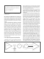
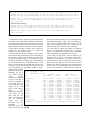
Have I Really Met Timing? - Validating PrimeTime Timing Reports with Spice Tobias Thiel Motorola GmbH, Semiconductor Products Sector, Munich, Germany, [email protected] Abstract At sign-off everybody is wondering about how good the accuracy of the static timing analysis timing reports generated with PrimeTime really is. Errors can be introduced by STA setup, interconnect modeling, library characterization etc. The claims that path timing calculated by PrimeTime usually is within a few percent of Spice don’t help to ease your uncertainty. When the Signal Integrity features were introduced to PrimeTime there was also a feature added that was hardly announced: PrimeTime can write out timing paths for simulation with Spice that can be used to validate the timing numbers calculated by PrimeTime. By comparing the numbers calculated by PrimeTime to a simulation with Spice for selected paths the designers can verify the timing and build up confidence or identify errors. This paper will describe a validation flow for PrimeTime timing reports that is based on extraction of the Spice paths, starting the Spice simulation, parsing the simulation results, and creating a report comparing PrimeTime and Spice timing. All these steps are done inside the TCL environment of PrimeTime. It will describe this flow, what is needed for the Spice simulation, how it can be set up, what can go wrong, and what kind of problems in the STA can be identified. 1. The Golden Reference for timing Static Timing Analysis has become the method of choice for timing sign off before tape out. Because of its superior analysis speed especially on chip-level and the completeness that no pattern set can provide it has pushed back simulation with timing to a state where it is only little more than an option on the flow chart in a modern design flow. Only very few customers for ASIC chips today require a chip level simulation with timing for acceptance of the silicon. As for timing simulation the basis for Static Timing Analysis is delay calculation. The goal of delay calculation is to predict the timing that the silicon reality 1530-1591/04 $20.00 (c) 2004 IEEE of all devices on the chip will show. But there is a pitfall: Due to process variations, temperature dependencies and the influence of voltage variations there is not one single silicon that can serve as a reference. When developing a new silicon technology a lot of time, money, and effort is spent on collecting statistical information on the variation of timing and other characteristics like power and reliability with process parameters, voltage, and temperature (PVT). From these statistical models the socalled transistor models in Spice format are generated. These are one of the fundamental bricks a silicon library is built of. They describe the characteristics of a transistor based on parameters like its length, width, and many more. It is because of these variations with PVT that the only predictable reference for the timing of a chip are the Spice models. It may sound bizarre, but it is the Spice models and not the finished silicon that is the golden reference for the design of an ASIC. Once a technology has been defined and validated it is the job of the fab or foundry to produce silicon that matches this reference and guarantee that the finished product will meet the specification. In a standard cell library a timing model for each cell is generated. To generate these timing models all active and passive components like transistors, capacitances and resistances are extracted from the cell’s geometry data. These extracted netlists are usually different from the ideal netists that were used to design the standard cells. In addition to the active elements that provide the functionality they contain all the parasitic elements resulting for example from the cell’s internal wiring that have a strong influence on the performance and drive characteristic of the cell. In a step called the timing characterization the extracted netlist is simulated in a number of environments like different input slopes and output loads for combinational gates. The timing numbers and drive characteristics gathered in these simulation runs is stored in tables or in polynomial models that form the timing library. When doing delay calculation for each cell the delay and transition time at the output is taken from the timing library. For all interconnects between the cells the delay and edge degradation is calculated from the parasitic capacitances and resistances of the wires. It is quite obvious that on the way from the golden reference, the extracted Spice netlist, to the calculated delays used for STA a number of approximations are taken that result in inaccurate results. During timing characterization only a limited number of reference simulations can be done to acquire the delay model in the timing library. For all operation conditions of the cells that don’t exactly match the conditions of the reference simulation the table entries of the library need to be interpolated. Also, the algorithms for calculating the interconnect delay, the signal edge degradation, and the effective load on a driver do approximations and are proprietary to the tool vendor. Therefore, the actual accuracy of the calculated delays is difficult to estimate. With the introduction of PrimeTime SI not only features for the analysis of crosstalk effects were added to the PrimeTime tool. Also the command write_spice_deck was added that allows you to write out a netlist for a Spice simulation of selected timing paths. The Spice netlist that is written out by this command is composed of the capacitances and resistances of interconnect wires and the spice netlists of all gates connected to this timing path. While of course a Spice simulation of a complete chip is in most cases not feasible, simulating just a fragment of the whole design takes only a few seconds or minutes. And since the netlist simulated here is the extracted netlist with all parasitic elements in the cell and the interconnect, such a Spice simulation can be used as the golden reference to measure your STA results against. The goal of such a Spice simulation can of course never be to fully verify a chip’s timing. But it can be a useful tool to validate that the timing library, the calculated delays, and the STA setup result in correct timing numbers and it can give the designer a feeling how accurate these results are compared to the golden reference. 2. What do I need for timing validation? The command in PrimeTime that is used to generate a netlist from a timing path for Spice simulation is write_spice_deck. This command was added in the 2001.08 release of PrimeTime and is part of the Signal Integrity extension of the tool. Therefore this feature requires a PrimeTime SI license and can not be used with the standard tool license. Table 1 shows the most important arguments of the write_spice_deck command. Probably the most important input for the Spice deck generation is a Timing Path object. This object contains all the information on the path through the circuit for which the Spice deck shall be written out. This Timing Path object can be generated using the PrimeTime command get_timing_paths that is very similar to the report_timing command. write_spice_deck \ -output <spice_file> \ -header <header_file> \ -sub_circuit_file <netlist_file> \ $timing_path Table 1: The most important arguments of the write_spice_deck command The basic components for any Spice simulation are the Spice models. These Spice models are stored in one or more Spice library files and contain the information on the basic components of your technology, like CMOS transistors, diodes, resistors, etc. These Spice models are only needed for the Spice simulation, not for the generation of the Spice deck in PrimeTime. However, The write_spice_deck command generates a complete deck for the Spice simulator that contains everything to start simulating, not only the netlist. Therefore, it is possible to specify a Spice header file when generating the deck. This header file contains a list of model libraries that need to be read in by the simulator. An example for such a header file is shown in Table 2. .lib .lib .lib .lib .lib .lib .lib .lib .lib .lib .lib /tsmc18/spice/mapped.rev2c /tsmc18/spice/mapped.rev2c /tsmc18/spice/mapped.rev2c /tsmc18/spice/mapped.rev2c /tsmc18/spice/mapped.rev2c /tsmc18/spice/mapped.rev2c /tsmc18/spice/mapped.rev2c /tsmc18/spice/mapped.rev2c /tsmc18/spice/mapped.rev2c /tsmc18/spice/mapped.rev2c /tsmc18/spice/mapped.rev2c BASE BSIM WCS_PARA WCS_FET WCS_IO DIODE RESISTOR DEFINES MOSFET WCS_NAIO WCS_NA Table 2: An Example for a Spice header file The .lib statement instructs the Spice simulator to read from a technology file the named library. As you can see there are not only libraries for elements like transistors and diodes but also libraries that define parameters for the process. What libraries are actually available and needed is specific to each technology. Often header files for the different process conditions are delivered with the library. If this should not be the case, once you have located the Spice library file you can search for the “.lib” statements inside this file and find out which libraries are available. Based on this it is easy to set up the header file. The final ingredient for the Spice deck extraction and the simulation are the extracted netlists for the standard cells. These netlists are the links between the standard cell based netlist that is used by PrimeTime and the basic elements that are used in Spice. Table 3 shows an example for such a netlist. The netlists for all standard cells need to be concatenated into a single file. Alternatively it is possible to generate a file referencing separate netlist files with the “.include” .subckt BUF Y A m_p1 vdd net1 Y vdd pch m_n1 Y net1 vss vss nch m_p0 vdd A net1 vdd pch m_n0 net1 A vss vss nch c1 net1 vss 6.52119E-16 c2 Y vss 2.48623E-16 c3 A vss 4.12536E-16 .ends l=0.18 l=0.18 l=0.18 l=0.18 w=1.80 w=1.20 w=0.75 w=0.50 Table 3: An example for the extracted netlist of a standard cell Spice statement. This global netlist file is passed to the write_spice_deck command with the -sub_circuit_file switch. PrimeTime will parse this file when generating the Spice deck to determine the pin order on the sub circuits that form the standard cells. If a cell is missing in the netlist file the PrimeTime tool will generate a warning message. Obtaining the complete and correct set of extracted netlists is sometimes the most challenging work when setting up the Spice simulation. In many library distributions only Spice netlists targeted for LVS analysis are available. These netlists usually don’t contain the parasitic elements and therefore result in inaccurate timing. You should always check that the netlists contain extracted parasitic elements like the three capacitors in the netlist in Table 3. If your design contains nonstandard cells like memories, obtaining the netlist for these blocks is usually even more challenging. Of course it is possible to extract a Spice netlist of a memory block from the layout, but the large number of elements probably will significantly impair your simulation time. In such a case you should consider to extract only a part of the memory like the access logic or maybe you can live with a dummy model. 3. The Spice deck generated by PrimeTime Although the write_spice_deck command of PrimeTime usually generates a complete Spice file that can be driver pin Driver V=0 directly simulated, there are some basic points you should know about the Spice deck to be able to debug or enhance the results. In the appendix you can find an example for a Spice deck generated by PrimeTime. At the beginning of the spice deck you will find the header that reads the model libraries, a definition of the supply voltages and the operating temperature, and an include statement to read the Spice netlist containing the standard cells. After that header section follows the timing path section. This part of the Spice deck contains the instantiations of the standard cells and the models for the wires between the cells. Of course the verification of the timing paths is most useful on a layouted design with an extracted netlist where detailed information on the interconnect is available. However, it is also possible to do a Spice simulation when PrimeTime works on Wire Load Models. In this case PrimeTime will place a capacitance with the value from the statistical Wire Load Model at the driver pin and connect the driver to the receiver using two voltage sources as shown in Picture 1. With this approach all timing points of the path, the driver pin, the net, and the receiver pin, are available in the Spice simulation. If your timing path contains nets with more than one receiver you will find that the generated spice deck not only instanciates the cells that are part of the timing path but all cells that are connected to the drivers of the path. This is important to know, because although these cells are only used to accurately model the load on the nets, also their elements are simulated. So if you want to do a Spice simulation on a netlist before clock tree insertion you might end up simulating hundreds or even thousands of flipflops all connected to the same clock signal. After the netlist of the timing path follows the dynamic voltage sources for the inputs that trigger the transition on the path. If the path doesn’t contain any sequential elements only the start point is driven by a dynamic source. In the example in the appendix you can see that there are two dynamic voltage sources. One source is for the clock signal that is the starting point of the timing path. The second dynamic source stimulates the data input of the flipflop in the path so that it is first initialized to net CWLM Picture 1: Interconnect modeling with Wire Load Models V=0 receiver pin Receiver high. After this input Investigating BUFX2... A(f)->Y(f): PrimeTime: 0.4393 Spice: 0.4411 Difference: 0.41% changes to low a falling A(r)->Y(r): PrimeTime: 0.3685 Spice: 0.3602 Difference: 2.31% edge at the output of the flipflop is triggered with the next clock event. In Table 4: An example for the output of verify_cell_timing addition to the dynamic Simulating just a single cell in Spice takes only a few voltage sources there are a number of static sources that seconds. So using this script it is possible to compare all set the inputs of the gates to defined values so that the timing arcs of all cells in a library to the Spice simulation. path you want to simulate is sensitized and the transition This can be started running the commands listed in Table can propagate through all cells. 5. At the very end of the Spice deck you can find a “.tran” statement. This tells the Spice simulator to run a transient read_db -library <library> analysis with the given minimal time resolution and set allcells {}; duration. foreach_in_collection cell \ [ sort_collection \ This Spice deck is sufficient to simulate the timing path. [ get_lib_cells "<libname>/*" ] ] { However, to analyze the results and to compare them to set allcells [ \ the PrimeTime timing there are some measurements concat $allcells \ needed. Probably the best way to add these measurements [ get_attribute $cell base_name ] \ ]; is to insert them into the Spice deck based on the timing } path the deck was generated from. This can be done in verify_cell_timing $allcells PrimeTime using a TCL script. Table 5: Verifying all cells of a library 4. The first step – validate your models and library When running a Spice simulation with a library for the first time it is helpful to take a step-by-step approach. At first you should always verify that the Spice model library and the extracted netlists you have for your standard cells give you the same timing behavior as the timing library that is read by PrimeTime. Although this sounds trivial there are severe differences that can occur here. One example is the correct scale of the transistor sizes. It is possible to define the unit for the dimensions of your transistors in the Spice setup. So if the width of a transistor in the netlist is given with “w=1.0” this could result in a transistor with a width of 1µm or 1m, depending on your scale setting. Using the TCL scripting interface of PrimeTime comparing the timing in the library against the Spice simulation can be easily automated. The script verify_cell_timing that you can find in the appendix can be used to create a small Verilog netlist instantiating a single cell to be tested. It reads in this Verilog netlist and applies one set of boundary conditions. For this test setup all possible timing paths are selected and Spice decks are generated. These Spice decks are than simulated, the simulation results are parsed and compared to the timing calculated in PrimeTime. Using this script a single cell can be verified using the command verify_cell_timing { BUFX2 } The script generates an output like in Table 4. Such a comparison of a whole library can easily be run over night. In such a comparison it is normal to have a difference of a few per cent on each timing arc. Since the Spice simulation is run only for one set of boundary conditions, depending on how well these match the conditions for which the cells were characterized, the difference will vary. It can happen that for complex gates such as a multiplexer the timing model in the library is incomplete or is not modeled correctly. Using this approach of verifying all timing arcs to Spice such modeling errors stick out by showing differences of more than 10%. 5. Generating a reference timing report When verifying the timing of a path through a single cell there are only two timing points on the path - the start point and the end point. Anything inside the cell is not visible to PrimeTime. This approach of just analyzing the delay from start to end point can of course also be used on more complex timing paths through more levels of logic. If the Spice simulation results in the same delay from start point to end point this information is sufficient. But if there should be a difference you will need more details for analyzing the source of the problem. The advantage of generating and triggering the Spice simulation from the PrimeTime shell is that you know which timing points can be found on the timing path. Also the names of the timing points in the Spice deck and the timing path object are identical. So it is easy to add additional measure statements to the Spice deck to access any timing number you need. * measure total delay .measure tran d_1_2 trig "v#ips_addr[7]" val=0.81 fall=1 targ "v#U73/B" val=0.81 fall=1 .measure tran d_1_3 trig "v#ips_addr[7]" val=0.81 fall=1 targ "v#U73/Y" val=0.81 fall=1 .measure tran d_1_4 trig "v#ips_addr[7]" val=0.81 fall=1 targ "v#U72/D" val=0.81 fall=1 (...) .measure tran d_1_15 trig "v#ips_addr[7]" val=0.81 fall=1 targ "v#U92/Y" val=0.81 rise=1 .measure tran d_1_16 trig "v#ips_addr[7]" val=0.81 fall=1 targ "v#ips_rdata[0]" + val=0.81 rise=1 * measure delta delay .measure tran d_2_3 trig "v#U73/B" val=0.81 fall=1 targ "v#U73/Y" val=0.81 fall=1 .measure tran d_3_4 trig "v#U73/Y" val=0.81 fall=1 targ "v#U72/D" val=0.81 fall=1 .measure tran d_4_5 trig "v#U72/D" val=0.81 fall=1 targ "v#U72/Y" val=0.81 fall=1 (...) .measure tran d_15_16 trig "v#U92/Y" val=0.81 rise=1 targ "v#ips_rdata[0]" + val=0.81 rise=1 Table 6: Measure statements that can be added to the Spice deck for a detailed analysis I found it most useful to generate a report that resembles from the simulation and compare it to the timing that was the output of the report_timing command in PimeTime. calculated by PrimeTime. Table 7 shows an example for This timing report shows the incremental delay for each such a report. It contains the delta and total delay for each cell and each interconnect between the cells on the timing stage of the timing path. From such a report you can path. In addition to that the total delay from the start point easily locate the source of differences in the timing. to each point on the path is reported. Table 6 shows an Of course there are endless possibilities for additional example for the measure section to acquire the analysis, for example the transition times at all timing information for such a detailed report. points of the path could be measured in the simulation When generating the measure statements you need to be and be compared to the calculated transition times. careful which voltage threshold to select. Depending on Such a report can only show if there are differences in the setting in your library the thresholds for delays could the delays and if there are, which cells or interconnects be 50% of the supply voltage, or for example 20% for a contribute to the difference. A possible reason for a rising edge and 80% for a falling edge. If the thresholds mismatch could be that the signal slope at some timing for the measurements are set differently than in your point exceeds the range for which the library cell was library you will find that the total path delay will be close characterized. This can happen on nets with high loads, to what you expect, but the delta delays for the cells and but also on nets with small load that have a strong driver. nets will sometimes be significantly smaller or larger. In these cases the slope is smaller than the smallest or Another challenge when PATH #1 generating the measure from: ips_addr[7] (fall) thresholds can be if to: ips_rdata[0] (rise) your design contains PrimeTime timing Spice timing pin edge delta total delta total several voltage domains. For example if ips_addr[7] fall 0.000000 0.000000 | 0.000000 0.000000 you have pad cells at U73/B fall 0.000044 0.000044 | 0.000043 0.000043 U73/Y fall 0.462108 0.462152 | 0.443418 0.443462 the start or end point of U72/D fall 0.000007 0.462159 | 0.000027 0.443489 your timing path you U72/Y fall 0.398624 0.860783 | 0.406903 0.850391 need to find the correct U70/A fall 0.000006 0.860789 | 0.000038 0.850429 voltage level for each U70/Y rise 0.127181 0.987970 | 0.110866 0.961295 U67/C rise 0.000015 0.987985 | 0.000082 0.961378 point on the path to U67/Y fall 0.137421 1.125406 | 0.130432 1.091809 trigger your U76/A fall 0.000018 1.125424 | 0.000084 1.091893 measurement correctly. U76/Y rise 0.140869 1.266293 | 0.129620 1.221513 The parser for the U78/A rise 0.000024 1.266317 | 0.000044 1.221557 U78/Y rise 0.331501 1.597818 | 0.318523 1.540080 Spice result file now U92/B rise 0.002680 1.600498 | 0.002659 1.542739 needs to be enhanced to U92/Y rise 0.158986 1.759484 | 0.168551 1.711290 read the simulation ips_rdata[0] rise 0.000003 1.759487 | 0.000009 1.711299 results back into PrimeTime is 2.82% off the Spice results. PrimeTime is pessimistic. PrimeTime. The TCL capabilities of PrimeTime can also be Table 7: A timing report comparing PrimeTime timing to the Spice simulation used to format the data results larger than the largest entry in the timing table. The delay calculation tool will in such a case extrapolate the value what can be quite inaccurate. Another example for an error that was found using the comparison to Spice was when a pad library was used that operated at 3.0 volt while the core cells operated at 1.5 volts. Since the pad library contained scalers to adjust for different pad voltages, the pad timing was accidentally calculated not for the 3.0 volt operating condition but for 1.5 volt. All I/O paths were calculated with about 2ns pessimistic timing. intended to be a complete solution for all types of Spice simulators and analysis details you may need. But I hope it will serve as a starting point for setting up and automating your verification process. To conclude, I can only encourage you to spend the effort and validate your STA results with a Spice simulation. Once you have set up the simulation, it is easy to impress your colleges and your boss with some plots from the analog world to prove that your Static Timing Analysis matches the golden references and that you have really met timing. 6. To the digital designer References [1] “PrimeTime User Guide: Fundamentals”, Synopsys, Version T-2002.09 [2] “PrimeTime User Guide: Advanced Timing Analysis”, Synopsys, Version T-2002.09 [3] “PrimeTime SI User Guide”, Synopsys, Version T-2002.09 [4] “HSPICE User’s Manual”, Meta-Software, Volume 1-3, California, 1992 [5] Brent B. Welch, “Practical Programming in TCL and TK”, 3rd Edition, Prentice Hall, 1999 Many digital design engineers shy the difficult setup of a Spice simulation and the high runtime on the designs that they usually work on. Therefore, very few consider doing reference simulations with Spice. However, using the interface to Spice that PrimeTime provides allows you to create the whole setup for simulating only that fraction of the circuit you are interested in with very little effort. The TCL script that is provided in the Appendix is not 7. Appendix 7.1 An example for a Spice deck generated by PrimeTime .lib /libraries/tsmc18/spice/mapped.rev2c BASE .lib /libraries/tsmc18/spice/mapped.rev2c BSIM .lib /libraries/tsmc18/spice/mapped.rev2c WCS_PARA .lib /libraries/tsmc18/spice/mapped.rev2c WCS_FET .lib /libraries/tsmc18/spice/mapped.rev2c WCS_IO .lib /libraries/tsmc18/spice/mapped.rev2c DIODE .lib /libraries/tsmc18/spice/mapped.rev2c RESISTOR .lib /libraries/tsmc18/spice/mapped.rev2c DEFINES .lib /libraries/tsmc18/spice/mapped.rev2c MOSFET .lib /libraries/tsmc18/spice/mapped.rev2c WCS_NAIO .lib /libraries/tsmc18/spice/mapped.rev2c WCS_NA * MIN. timing path section: (rising) timer_1/counter_buf_reg_3_/ck -> (falling) ips_rdata[3]. .global vdd vss vvdd vdd 0 1.35 vvss vss 0 0 .temp 150 *.prot .include "/home/tobias/spice_netlist" *.unprot * Timing path section: (rising) timer_1/counter_buf_reg_3_/ck -> (falling) ips_rdata[3]. (...) * Timing path cell 2: falling U16/d1 -> falling U16/x * The side pin ’U16/d0’ is sensitized to ’low’. * The side pin ’U16/sl0’ is sensitized to ’high’. ****************************************** * SPICE pin order used. * .pin(sub_node): .X(U16/x) .D0(U16/d0) .D1(U16/d1) .SL0(U16/sl0) xU16 U16/x U16/d0 U16/d1 U16/sl0 mux2_2 ****************************************** * Timing path net 2 : falling ips_rdata[3] * resistor(s) for net ’ips_rdata[3]’. * driver pin ’U16/x’. r00100 ips_rdata[3]:1 ips_rdata[3] r00101 ips_rdata[3] ips_rdata[3]:3 r00102 ips_rdata[3]:3 ips_rdata[3]:4 r00103 ips_rdata[3]:3 ips_rdata[3]:6 r00104 ips_rdata[3]:3 ips_rdata[3]:13 r00105 ips_rdata[3]:3 ips_rdata[3]:12 r00106 ips_rdata[3]:17 U16/x r00107 ips_rdata[3]:17 ips_rdata[3]:5 r00108 ips_rdata[3]:17 ips_rdata[3]:15 r00109 ips_rdata[3]:17 ips_rdata[3]:18 r00110 ips_rdata[3]:18 ips_rdata[3]:10 r00111 ips_rdata[3]:18 ips_rdata[3]:7 r00112 ips_rdata[3]:6 ips_rdata[3]:14 r00113 ips_rdata[3]:6 ips_rdata[3]:7 r00114 ips_rdata[3]:6 ips_rdata[3]:11 r00115 ips_rdata[3]:7 ips_rdata[3]:9 r00116 ips_rdata[3]:7 ips_rdata[3]:8 * ground capacitors(s) for net ’ips_rdata[3]’. c00102 ips_rdata[3]:1 0 0.001f c00103 ips_rdata[3] 0 0.065391f c00104 ips_rdata[3]:3 0 0.0247121f c00105 ips_rdata[3]:4 0 0.421554f c00106 ips_rdata[3]:5 0 0.162986f c00107 ips_rdata[3]:6 0 0.087714f c00108 ips_rdata[3]:7 0 0.0328137f c00109 ips_rdata[3]:8 0 0.001f c00110 ips_rdata[3]:9 0 0.0122159f c00111 ips_rdata[3]:10 0 0.001f c00112 ips_rdata[3]:11 0 0.0249453f 0.76725 2.5916 0.01 1.7 0.01 0.01 0.01 0.01 0.01 1.4322 0.01 1.7 0.01 0.01 0.01 0.01 0.01 c00113 c00114 c00115 c00116 c00117 c00118 c00119 ips_rdata[3]:12 ips_rdata[3]:13 ips_rdata[3]:14 ips_rdata[3]:15 U16/x ips_rdata[3]:17 ips_rdata[3]:18 0 0 0 0 0 0 0 0.00125659f 0.001f 0.001f 0.001f 0.001f 0.001f 0.001f (...) ****************************************** * INFO: PrimeTime created the following PWL or voltage source. * Please verify. ****************************************** * Timing path sequential data pin voltage section: (rising) timer_1/counter_buf_reg_3_/ck > (falling) ips_rdata[3]. ********** Arrival Window Info. for pin ’timer_1/counter_buf_reg_3_/d’ ********** * {clk} pos_edge {min_r_f 3.47638 3.54304} {max_r_f 5.73091 6.00015} * clock {rise fall}: {0 5} * For rising pwl *vtimer_1/counter_buf_reg_3_/d timer_1/counter_buf_reg_3_/d 0 pwl(0.0ns 0 *+ 13.4263ns 0 *+ 13.5376ns 1.35) * For falling pwl vtimer_1/counter_buf_reg_3_/d timer_1/counter_buf_reg_3_/d 0 pwl(0.0ns 1.35 + 13.4881ns 1.35 + 13.6102ns 0) * End of timing path sequential data pin voltage section * Timing path clock tree input voltage section: (rising) timer_1/counter_buf_reg_3_/ck -> (falling) ips_rdata[3]. ****************************************** vclk clk 0 pulse ( 0 1.35 11.2333ns 1.66667ns 1.66667ns 3.33333ns 10ns ) ****************************************** (...) ****************************************** * The side pin ’U16/d0’ of cell ’U16’ (mux2_2) * is set to ’low’ by sensitization. vU16/d0 U16/d0 0 0 ****************************************** * The side pin ’U16/sl0’ of cell ’U16’ (mux2_2) * is set to ’high’ by sensitization. vU16/sl0 U16/sl0 0 1.35 (...) * transient analysis .tran 0.1ns 50ns .end 7.2 TCL script to automatically compare the timing of library cells to Spice simulation ### set set set set set some global variables spice_header "/home/tobias/spice_header"; spice_netlist "/home/tobias/spice_netlist"; default_input_slope 1.0; default_output_load 0.05; supply_voltage 1.62; ############################################################################## # Compare the timing of the listed cells to Spice simulation ############################################################################## proc verify_cell_timing { cells } { global link_path default_input_slope default_output_load; ### read in all libraries in $link_path if { [ get_libs * -quiet ] == "" } { foreach lib $link_path { if { [ string match "*.db" $lib ] } { read_db -library $lib; } } } foreach cell $cells { ### create verilog netlist set libcell [ create_testcase_for_cell $cell "tmp_netlist.v" ]; if { $libcell == -1 } { continue; } puts "Investigating $cell..."; ### read design remove_design -all >> /dev/null; read_verilog tmp_netlist.v >> /dev/null; link >> /dev/null; ### create a virtual reference clock and apply conatraints create_clock -period 10.0 -name ref_clock; set_input_transition $default_input_slope [ all_inputs ]; set_load $default_output_load [ all_outputs ]; set_input_delay -clock ref_clock 5.0 [ all_inputs ]; ### create real clock on clock inputs foreach_in_collection pin [ get_lib_pins -of_object $libcell ] { if { [ get_attribute $pin is_clock_pin ] == "true" } { set clock [ get_attribute $pin base_name ]; create_clock -period 10.0 $clock; set_propagated_clock $clock; } } foreach_in_collection path [ get_timing_path -delay_type max -nworst 1000 \ -to [ all_outputs ] ] { verify_path_timing $path; }; # foreach_in_collection path }; # foreach cell } ############################################################################## # Create a testcase verilog file instanciating a single test cell ############################################################################## proc create_testcase_for_cell { cell filename } { ### search for library cell foreach_in_collection lib [ get_libs * ] { set libname [ get_attribute $lib full_name ]; set libcell [ get_lib_cells "$libname/$cell" -quiet ]; if { $libcell != "" } { break; } } if { ![ info exists libcell ] || $libcell == "" } { puts "Error: could not find cell ’$cell’ in any library!"; return -1; } ### create string lists foreach_in_collection pin [ get_lib_pins -of_object $libcell ] { set pinname [ get_attribute $pin base_name ]; set pindir [ get_attribute $pin pin_direction ]; append portlist ", $pinname"; append pinlist ", .$pinname\($pinname\)"; append iolist "\n $pindir\put $pinname;"; } ### write testcase file set FILE [open $filename "w"]; puts $FILE [ format "module verification_top (%s);" \ [ string trimleft $portlist ", " ]]; puts $FILE [ string trimleft $iolist ", " ]; puts $FILE ""; puts $FILE [ format " $cell DUT (%s);" [ string trimleft $pinlist ", " ]]; puts $FILE "endmodule"; close $FILE; return $libcell; } ############################################################################## # Run Spice simulation on a timing path, parse and compare the results ############################################################################## proc verify_path_timing { path } { global spice_header spice_netlist supply_voltage; ### create the Spice deck write_spice_deck -output spice.pt \ -header $spice_header \ -sub_circuit_file $spice_netlist \ $path; ### add a measure statement to the spice deck for the path delay sh sed -e "s/^.print/* .print/" -e "s/^.unprot/* .unprot/" \ -e "s/^.prot/* .prot/" -e "s/^.end/* .end/" spice.pt > spice.ckt set set set set set set points [ get_attribute $path points ]; size [ sizeof_collection $points ]; startpoint [ index_collection $points 0 ]; endpoint [ index_collection $points [ expr $size - 1 ] ]; startname [ get_attribute [ get_attribute $startpoint object ] full_name ]; endname [ get_attribute [ get_attribute $endpoint object ] full_name ]; regsub -all "/" $startname "?" startname regsub -all "/" $endname "?" endname echo [ format ".measure tran delay trig v(%s) val=%f %s=1" \ $startname \ [ expr $supply_voltage * 0.5 ] \ [ get_attribute $startpoint rise_fall ] ] >> spice.ckt echo [ format "+ targ v(%s) val=%f %s=1" \ $endname \ [ expr $supply_voltage * 0.5 ] \ [ get_attribute $endpoint rise_fall ] ] >> spice.ckt echo ".end " >> spice.ckt #!!!!!!!!!!!!!!!!!!!!!!!!!!!!!!!!!!!!!!!!!!!!!!!!!!!!!!!!!!!!!!!! # The following command is specific for the Spice simulator used. # This needs to be customized for different simulators. #!!!!!!!!!!!!!!!!!!!!!!!!!!!!!!!!!!!!!!!!!!!!!!!!!!!!!!!!!!!!!!!! exec <your spice simulator> -b spice.ckt >& spice.result; ### parse the simulation output set spice_delay [ parse_result_file "spice.result"]; ### print result print_result $startpoint $endpoint $spice_delay; } ############################################################################## # Parse the simulation results # This may need to be changed for a different Spice simulator ############################################################################## proc parse_result_file { file } { set FILE [open $file "r"] set last_line "" set spice_delay -1.0; while { [ gets $FILE line ] >= 0 } { if { [ string match {-*} $last_line ] } { [ scan $line "%s %s %s %s %s" field1 field2 field3 field4 field5] if { ![ string match "delay" $field1 ] && \ ![ string match "failed" $field1 ] } { set spice_delay [ expr $field1 * 1.0e+9 ]; } } set last_line $line } close $FILE ### For flipflops, substract 1 clk period for the event is triggered with ### the 2nd clk event. if { $spice_delay > 10.0 } { return [ expr $spice_delay - 10 ]; } return $spice_delay; } ############################################################################## # Format and print the result ############################################################################## proc print_result { startpoint endpoint spice_delay } { set lib_delay [ expr [ get_attribute $endpoint arrival ] \ - [ get_attribute $startpoint arrival ] ]; if { $spice_delay > $lib_delay } { set diff [ expr ($spice_delay - $lib_delay) * 100.0 / $spice_delay ]; } else { set diff [ expr ($lib_delay - $spice_delay) * 100.0 / $lib_delay ]; } puts [ format "%s(%s)->%s(%s): PrimeTime: %.4f Spice: %.4f Difference: %.2f%%" \ [ get_attribute [ get_attribute $startpoint object ] full_name ] \ [ get_attribute $startpoint rise_fall ] \ [ get_attribute [ get_attribute $endpoint object ] full_name ] \ [ get_attribute $endpoint rise_fall ] \ $lib_delay $spice_delay $diff ]; } # EOF