1
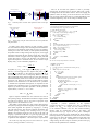
a
b
f
fa
fb
f
fa
fc
fb
fc
1
PE(v)
pwr(v)
Slack Redistribution for Graceful Degradation
Under Voltage Overscaling
a
b
†+
I. I NTRODUCTION
The traditional goal of IC design is for the product to always
operate correctly, even under worst-case combinations of (process, voltage, temperature, wear-out, etc.) non-idealities. It is wellrecognized that designing for worst-case operating conditions incurs
considerable area, power and performance overheads [5], and that
these overheads worsen with increased manufacturing or runtime
variations in advanced technology nodes [24]. Better-than-worst-case
(BTWC) design [1] allows reliability (in the sense of timing and
hence functional correctness) to be traded off against performance
and power. The central idea, as exemplified by the shadow-latch
technique in Razor [5], is to design for average-case conditions
(thus saving area and power) while adding an error detection and
correction mechanism to handle errors that occur with worst-case
variabilities. System-level techniques, as exemplified by Algorithmic
Noise Tolerance [13], allow timing errors to proliferate into the
system or application, but then exploit algorithmic and/or cognitive
noise tolerance in mitigating errors at the application level. The use
of such application- or system-level error detection and correction is
assumed in proposed probabilistic SOCs [3] and stochastic processor
architectures [18], which are recent classes of BTWC designs.
Our work focuses on the optimized application of voltage overscaling for power reduction in the context of BTWC design. Figure 1 illustrates power consumption under voltage scaling in BTWC
designs. In the left plot, functional errors begin to occur below the
voltage vb , but we can reduce power consumption until we reach the
voltage vc , given the use of error correction. The right plot shows
that below the voltage vc , power consumption is increased because
of recovery overhead.
The impact of BTWC design techniques is often limited in highperformance digital designs by a critical operating point or “wall
of slack” phenomenon that limits voltage overscaling and, more
importantly, is a direct consequence of today’s standard approach to
power optimization. The Critical Operating Point (COP) hypothesis
[19] (cf. Figure 1(a)), in the context of voltage scaling, states that a
c
a
b
va vb vc
(a)
v
Power consumption
Abstract—Modern digital IC designs have a critical operating point,
or “wall of slack”, that limits voltage scaling. Even with an errortolerance mechanism, scaling voltage below a critical voltage - so-called
overscaling - results in more timing errors than can be effectively
detected or corrected. This limits the effectiveness of voltage scaling
in trading off system reliability and power. We propose a designlevel approach to trading off reliability and voltage (power) in, e.g.,
microprocessor designs. We increase the range of voltage values at
which the (timing) error rate is acceptable; we achieve this through
techniques for power-aware slack redistribution that shift the timing
slack of frequently-exercised, near-critical timing paths in a power- and
area-efficient manner. The resulting designs heuristically minimize the
voltage at which the maximum allowable error rate is encountered, thus
minimizing power consumption for a prescribed maximum error rate
and allowing the design to fail more gracefully. Compared with baseline
designs, we achieve a maximum of 32.8% and an average of 12.5% power
reduction at an error rate of 2%. The area overhead of our techniques,
as evaluated through physical implementation (synthesis, placement and
routing), is no more than 2.7%.
Errors/Time
c
Andrew B. Kahng , Seokhyeong Kang† , Rakesh Kumar‡ cand John Sartori‡
† ECE and + CSE Departments, University of California
b
a
at San Diego
‡ Coordinated Science Laboratory, University of Illinois
v
(lower voltage)
va vb vc
va vb vc [email protected]
[email protected], [email protected], [email protected],
(lower voltage)
v
a
b
c
va vb vc
v
(b)
Fig. 1. Error rate (a) and power consumption (b) versus voltage scaling in
BTWC designs.
modern digital design will have a critical operating voltage Vc above
which zero timing errors occur, and below which massive timing
errors occur. The COP hypothesis is natural in light of how modern
designs are optimized for power and area, subject to a frequency
constraint: negative timing slack (on a combinational path) is cured
by upsizing and buffering, while positive timing slack is traded off
for area and power reductions. Thus, in the final design, many timing
paths are critical, and there is a “wall of (critical) slack”. The COP
hypothesis states that overscaling beyond the critical voltage can
abruptly cause error rates beyond what an error-tolerance mechanism
can handle. According to [19], this has been confirmed in generalpurpose microprocessors. A key motivation for our work is that COP
behavior limits the applicability of voltage scaling in trading off
reliability for power - even in the context of BTWC design.
Our work seeks to improve the effectiveness of BTWC design
techniques through power-aware slack redistribution, a novel design
approach that enables extended voltage-reliability tradeoffs. Poweraware slack redistribution reapportions timing slack of frequently occurring, near-critical timing paths to increase the level of overscaling
(i.e., reduce the minimum voltage) at which a given error-tolerance
mechanism can maintain an acceptable timing error rate. The result
is a design that fails more gracefully, and achieves significantly
improved power savings with only small degradation of application
performance.
In the following, Section II reviews previous work, and Section III
formalizes the problem of achieving “gradual slope” in the timing
slack distribution, and hence graceful degradation of correctness with
voltage overscaling. Section IV describes our power-aware slack redistribution techniques, and Section V discusses implementation and
experimental methodology. Section VI presents results and analysis,
and Section VII concludes.
II. R ELATED W ORK
A. BTWC Designs
Better-than-worst-case (BTWC) design approaches allow circuits
to save power by optimizing for normal operating conditions rather
than worst-case conditions. One class of BTWC techniques allows
adaptation to runtime conditions by specifying multiple safe voltage
and frequency levels at which a design may operate, and allows for
0
Timing slack
Zero slack after voltage scaling
B. Design-level Optimizations
Design-level optimizations for timing speculation architectures
([8], [20], [7]) identify and optimize frequently-exercised timing
paths, while other (infrequently-exercised) paths are allowed to have
timing errors. EVAL [20] trades error rate for processor frequency
by using system-level configurations to shift or otherwise reshape
path delay distributions of various functional units. BlueShift [8]
is an application of EVAL that identifies most frequently violated
timing constraints and optimizes the corresponding timing paths using
forward body biasing and path constraint tuning (PCT) (essentially,
setup timing over-constraints). CRISTA [7] also addresses variationtolerant circuit design by using Shannon expansion-based partitioning
to isolate critical paths. Critical paths with low activity are separated
and de-optimized.
C. Cell Sizing
Many previous works use cell sizing for power or area recovery
subject to timing constraints. Generally, positive (setup) timing slack
on non-timing critical cell instances can be flexibly ‘traded’ for power
and area objectives (gate-length increase or Vth swap to reduce
leakage, or gate-width decrease to reduce area and total power).
Fishburn and Dunlop propose a fast iterative method to meet delay
constraints called TILOS [6]. TILOS uses the Elmore delay model
for transistor delays, and proposes a heuristic that sizes transistors
iteratively, according to the sensitivity of the critical path delay to
the transistor sizes, i.e., finding a greedy (maximum delay reduction
/ transistor width increase) “move” at each iteration. The method
of Duet [21] performs simultaneous assignment of threshold voltage
(Vth ) and transistor width using a merit (sensitivity) function. Gupta
et al. propose small biases of transistor gate length to further minimize
leakage power [10]. They also present a sensitivity-based downsizing
approach for transistor-level Vth assignment [9], and a post-layout,
post-signoff gate length biasing technique for parametric yield (leakage and leakage variability) optimization [11]. Jeong et al. revisit a
general linear programming (LP) formulation that can concurrently
exploit multiple knobs ranging from multi-Lgate footprint-compatible
libraries to post-layout Lgate biasing [14].
Our work, detailed below, uses post-layout cell resizing to redistribute timing slack so as to achieve a switching activity-aware
‘gradual slope’ distribution of timing slack. We believe that ours is
the first to do so specifically in the BTWC context; moreover, our
proposed methodology can find frequently exercised paths rapidly
(without repeated gate-level simulation as in BlueShift).
III. T HE G OAL OF D ESIGN O PTIMIZATION
We minimize power consumption for a given error rate by minimizing the voltage at which that error rate can still be observed.
Traditional designs exhibit a critical wall of slack in which the path
slacks for the majority of paths are similar and close to the critical
path slack of the circuit (observe the red curve in Figure 2).
For traditional designs, our goal of aggressively reducing the
operating voltage to save power is thwarted by the critical wall of
slack, because scaling past the wall results in a catastrophic number
of timing violations. To alleviate this restraint, we seek to reshape
2
the slack distribution of a circuit to have a gradual slope rather than
the steep slope that characterizes the critical wall (observe the blue
curve in Figure 2).
‘wall’ of slack
Number of paths
switching between these states. Examples in this class are Correlating
VCO [2], [12] and Design-Time DVS [23]. Another class of BTWC
designs uses “canary” circuits, including delay-line speed detectors
[4] and triple-latch monitors [16], to detect when critical timing
(failure) is imminent and thus avoid any unsafe voltage scaling.
Finally, Razor [5] and ANT techniques [13] provide error tolerance
at the circuit- and algorithm-level, respectively. Their benefits under
voltage scaling are limited not only by COP behavior but by the
overhead of error correction that is increasingly required as voltage
is scaled.
0
‘gradual slope’ slack
Frequently
exercised
paths
Rarely
exercised
paths
Zero slack at
nominal voltage
Zero slack after voltage
scaling
Timing slack
Fig. 2. The goal of the ‘gradual slope’ slack optimization is to transform a
slack distribution having a critical ‘wall’ into one with a more gradual failure
characteristic.
To achieve the desired slack distribution that permits aggressive
voltage scaling, we must alter the slack of some paths to break
down the critical wall. In our optimization approach, we increase
the slack of frequently executed critical paths to reduce the onset of
errors when voltage is scaled. Likewise, we can reduce the slack of
rarely exercised paths, since these paths will not have a significant
impact on error rate when voltage is scaled. Together, these path
slack adjustments will reshape the slack distribution of a circuit and
extend the range of voltage scaling. The goals of our optimization
are expressed in Figure 2.
IV. S LACK R EDISTRIBUTION AND P OWER R EDUCTION
We now present our cell swapping approach to achieve a gradual,
activity- (and hence power-) aware timing slack distribution for a
given circuit design.
A. Power-aware Slack Redistribution Using Cell Swap Method
Our slack distribution optimizer is implemented in C++ and performs cell swapping (gate sizing only, with no logic resynthesis) using
the Synopsys PrimeTime vB-2008.12-SP2 [27] tool and its built-in Tcl
socket interface. Traditional optimization tools treat all paths equally:
all negative-slack paths must be brought up to zero or positive slack.
By contrast, to improve the performance-power profile of the design,
we spend our optimization efforts on frequently-exercised paths in
order to minimize error rates under voltage overscaling.
Our heuristic determines a target voltage corresponding to a
specific error rate, and then ‘over-optimizes’ frequently-exercised
paths using upsizing (i.e., increase of transistor width and hence drive
strength) cell swaps. Figure 3 illustrates the challenges inherent in
setting the target voltage. The figure shows path delay changes after
slack optimization for a fixed target voltage, where the optimizer
swaps cells in Paths A, B and C to reduce the slack of those paths
with respect to the fixed target voltage. However, if the voltage at
which the maximum acceptable error rate is observed is larger than
the target voltage as specified by the red-dotted line, Paths A and
C are optimized unnecessarily beyond the actual scaled voltage, and
power is wasted.
Our slack optimization approach finds a target voltage after estimating error rates at each operating voltage, and iteratively optimizes
paths while scaling voltage. At the initially selected voltage, the optimizer performs cell swaps to improve timing slack. After performing
this timing optimization at the initially selected voltage, the voltage
is scaled until the target error rate is reached. Figure 4 illustrates the
optimization heuristic. Path A is optimized until the target voltage is
reached, but Path C is not optimized, since Path C does not have
negative slack at the target voltage.
3
Negative Slack of Path A
at the target voltage
Actual voltage at the
target voltage
error rateat
Actual
Negative Slack of
Path A at the target
voltage
the target error
rate
Path A
Path
PathB A
Path
PathC B
Path C
Target voltage
(fixed)voltage
Target
Nominal
voltage
Nominal
Unnecessary cell
sizing cell
Unnecessary
sizing
(fixed)
voltage
Target voltage
Target(fixed)
voltage
(fixed)
Fig. 3. Path delay before and after slack optimization with a fixed target
voltage.
Find target voltage and
optimize
Find
target iteratively
voltage and
Negative Slack of Path A
Negative
Slack
of Path A
at the target
voltage
optimize iteratively
at the target voltage
Path A
Path A
Path B
Path B
Path C
Path C
Nominal Target
Target
voltage
with
Nominal
voltage
with
the the
voltage
estimated
error
voltage
estimated
error
raterate
New
targetvoltage
voltage
Target
Fig. 4. Target voltage and path slack before and after slack optimization
using the heuristic.
To enable proper voltage selection, we must accurately forecast
error rates without resorting to time-consuming functional simulation.
Accurate error rate estimation ensures that we do not over-optimize,
resulting in too much area overhead, or under-optimize, thus limiting
the possible extent of voltage scaling. For this purpose, we use toggle
information of flip-flops that have negative timing slack. The toggle
information consists of toggles from both negative-slack paths and
positive-slack paths; in the error rate calculation, only toggles from
negative-slack paths are considered. Hence, the error rate in a single
flip-flop, ER f f , can be estimated by Equation (1).
- since we do not allow the optimizer to touch a previouslyswapped cell; the intuition here is that this helps avoid ’cycling’
of configurations and also reduces runtime. After cell swapping, the
optimizer checks the timing of fan-in and fan-out cells that have
been previously touched. When there is no timing degradation in the
connected neighboring cells, the cell change is finally accepted.
Algorithm 1 Pseudocode for the slack optimizer.
Procedure SlackOptimizer( )
1. Read netlist and initialize PrimeTime Tcl socket interface;
2. Read switching activity (toggle rate) of each cell;
3. //Scale and find target voltage
4. for Vtarget = 1.00V to 0.50V; Vtarget ← Vtarget −0.01V do
5.
Load Library (.lib) for the target voltage Vtarget ;
6.
ER ← ComputeErrorRate(Vtarget );
7.
if ER > ERtarget then
8.
P ← FindCriticalPaths();
9.
OptimizePaths(P);
10.
else
11.
continue
12.
end if
13.
//Terminate algorithm after checking error rate and power
14.
ER ← ComputeErrorRate(Vtarget );
15.
PW R ← ReportTotalPower(Vtarget );
16.
if PW R > PW R prev then
17.
RestoreSwaps(); break;
18.
else if ER > ERtarget then
19.
break;
20.
else
21.
PW R prev ← PW R; continue;
22.
end if
23. end for
24. Save list of swaps and perform ECO with SOCE;
Procedure OptimizePaths(P)
ER f f = T G f f
∑ T Gp
×
∑ T Gp
neg
(1)
all
In Equation (1), T G f f is the toggle rate of flip-flop f f , T G p neg
and T G p all are the toggle rates of a negative slack path p neg and
all paths p all to flip-flop f f . We obtain an aggregate error rate as
the summation of error rates in all flip-flops. However, this value
will be significantly larger than the actual error rate observed during
functional simulation, it does not account for errors that occur in the
same clock cycle. Moreover, the existence of false paths also imparts
pessimism to the estimated error rate. We therefore use a parameter
α, obtained from experimental investigations, to compensate for this
pessimism. The estimated error rate of a target design D is defined in
Equation (2), with the compensation parameter α. In the experiments
reported below, a value of α = 0.5 is used.
ERD = α ×
∑
ER f f
(2)
f f ∈D
Figure 6 compares estimated error rates and actual error rates at
each operating voltage. The estimated error behavior roughly matches
the actual error behavior, and we can find an appropriate target
voltage based on the estimated error rate.
After finding a target voltage, the slack optimizer finds negativeslack paths by tracing backward from flip-flop cells using a depth-first
search (DFS) algorithm. We optimize by swapping (i.e., resizing)
cells with other library cells that have identical functionality. We
determine priority according to the switching activity of a path,
defined as the minimum toggle rate over all cells in the path. Cell
swapping is performed on all cells in a given target path, and only
swaps that improve timing slack of the path are accepted. 1 There
is significant order-dependence - and hence impact of prioritization
1 We consider only setup timing slack, since hold violations can typically
be fixed by inserting hold buffers in a later step.
1. while P 6= 0/ do
2.
Pick the critical path p with maximum switching activity;
3.
P ← P − p;
4.
while swap count is not zero do
5.
for i = 0 to |p| do
6.
if f lagc(i) then
7.
continue;
8.
end if
9.
for all alternative LibCell for the cell instance c(i) do
10.
Resize the instance c(i) with LibCell;
11.
Check the path slack of p;
12.
for all fanin and fanout cell c f an of c(i) do
13.
if f lagc f an then
14.
Check the slack of critical path p f an of c f an ;
15.
end if
16.
end for
17.
if ∆slack(p) < 0 or ∆slack(p f an ) < 0 then
18.
Restore cell change;
19.
end if
20.
f lagc(i) ← true;
21.
end for
22.
end for
23.
end while
24. end while
Algorithm 1 presents pseudocode of the optimizer.
ComputeErrorRate(Vtarget ) estimates error rates, as defined by
Equation (2). ERtarget is a target error rate, which can be set
to the maximum allowable error rate. The FindCriticalPaths()
function finds all negative-slack paths in the design, and
ReportTotalPower(Vtarget ) reports the total power consumption
from Synopsys PrimeTime. In the pseudocode, the target voltage is
iteratively scaled by an additional 0.01V until the error rate exceeds
a target error rate. Then, the heuristic optimizes critical paths at the
target voltage. If the power consumption is not reduced after the
voltage scaling, the latest swaps are restored by the RestoreSwaps()
function and the optimization is terminated.
4
Algorithm 2 Pseudocode for the power reduction.
Procedure PowerReduction( )
1. SlackOptimizer( );
2. Insert all cells into set C;
3. while C 6= 0/ do
4.
Pick the cell c and check the cell slack dc and toggle rate T gc ;
5.
if dc > 0 or T gc < β then
6.
for all alternative LibCell for the cell instance c(i) do
7.
Resize the instance c(i) with LibCell;
8.
Check the total power pw of the cell c;
9.
for all fanin and fanout cell c f an of c(i) do
10.
if ∆slack(c f an ) < 0 and T gc f an > γ then
11.
Restore cell change;
12.
else if pwc(i) > pwc(i−1) then
13.
Restore cell change;
14.
end if
15.
end for
16.
end for
17.
end if
18.
C ← C − c;
19. end while
20.
Save list of swaps and perform ECO with SOCE;
Gate-level
Initial design
Final design
simulation
We use the OpenSPARC T1 processor [25] to test our optimization
framework. Table I describes the selected modules and provides
characterization in terms of cell count and area.
TABLE I
TARGET MODULES FOR EXPERIMENTS .
Module
Stage
Description
Cell #
Area (um2 )
lsu dctl
lsu qctl1
lsu stb ctl
sparc exu div
sparc exu ecl
sparc ifu dec
sparc ifu errdp
sparc ifu fcl
spu ctl
tlu mmu ctl
MEM
MEM
MEM
EX
EX
FD
FD
FD
SPU
MEM
L1 Dcache Control
LDST Queue Control
ST Buffer Control
Integer Division
Execution Unit Control Logic
Instruction Decode
Error Datapath
L1 Icache and PC Control
Stream Processing Control
MMU Control
4537
2485
854
4809
2302
802
4184
2431
3341
1701
13850
7964
2453
14189
7089
1737
12972
6457
9853
5113
Gate-level simulation is performed using test vectors obtained from
full-system RTL simulation of a benchmark suite consisting of bzip2,
equake and a sorting test program. These benchmarks are each fastforwarded by 1 billion instructions using the OpenSPARC T1 system
simulator, Simics [17] Niagara. After fast-forwarding in Simics, the
B. Power-aware Post-processing
architectural state is transferred to the OpenSPARC RTL using CMU
Switching activity
ECO P&R
Design information
In addition to the above
slack optimization,
we can also reduce Transplant [22]. More details of our architecture-level methodology
(.v .spef)
(.saif)
(SOCEncounter)
power consumption by downsizing cells on rarely-exercised paths. are available in [15].
Algorithm 2 shows this post-processing heuristic. List
Theof power reSwitching activity data gathered from gate-level simulation is
swaps
Tcl Socket
duction procedure downsizes cells logical
equivalents with smaller fed to Synopsys PrimeTime (PT) static timing tool through its Tcl
I/F
Synopsys
powerLiberty
consumption. Two
parameters govern Slack
cell selection
socket interface. Timing slack and switching activity information
PrimeTime
Optimizer and swap
(.lib)
acceptance. First, a cell is selected that has positive slack or isLibrary
in Charic.
is continually available from PT, through the Tcl socket interface,
(SignalStorm)
a rarely-exercised path. The cell’s toggle rate should be less than
during the optimization process. After our optimization, all netlist
β, where the parameter β is set small enough for us to expect an changes are realized using Cadence SoC Encounter v7.1 [29] in ECO
insignificant effect on error rate. Downsizing cell swaps are accepted (engineering change order) mode.
as long as they do not increase error rate; to this end, a second variable
Module designs are implemented in TSMC 65GP technology using
γ characterizes the cell’s effect on neighboring cells. If the timing a standard flow of synthesis with Synopsys Design Compiler vYcharacterization
Initial
designhave largerLibrary
Benchmark
slack
of thegeneration
neighboring cells
which
toggle
rate than γ, 2006.06-SP5 [26] and place-and-route with Cadence SoC Encounter.
(Simics)
(SignalStorm)
(OpenSPARC T1)
the downsizing is restored. Within these constraints, the optimizer As noted above, voltage scaling effects are captured by characterizing
selects the Input
bestvector
candidate cells to Design
reduce
power without affecting Synopsys Liberty libraries (using Cadence SignalStorm TSI61) at a
information
Synopsys
error rate.
number of operating voltages. Runtime is reduced by adopting a
(.v .spef)
Liberty
Functional simulation
restricted library of 63 commonly-used cells (62 combinational and
(.lib)
(NC Verilog)
1 sequential); the total characterization time for 51 voltage points is
Tcl Socket
V. M ETHODOLOGY
around two days, but this is a one-time cost.
I/F
PrimeTime
Using our slack optimizer, we optimize the module implementaFigure 5 illustrates our PowerOptimizer
overall flow for gradual-slope
slack opSimulation dump (.vcd)
timization. The switching activity interchange format (SAIF) file tions listed in Table I, and then estimate error rates by counting cycles
List ofnet
swaps
provides toggling frequency for each
and cell in the gate-level with timing failures during gate-level simulation. We use a SCANnetlist; it is derived from a value change dump (VCD) file from like test wherein the test vectors specify the value of each primary
ECO P&R
gate-level simulation using(SOCEncounter)
in-built functionality ofFinal
the design
Synopsys input and internal flip-flop at each cycle. This prevents pessimistic
PrimeTime-Px [27] tool. To find timing slack and power values at error rates due to erroneous signals propagating to other registers.
the specific voltages, we prepare Synopsys Liberty (.lib) files for each We emulate the SCAN test by connecting all register output ports to
voltage value – from 1.00V to 0.50V in 0.01V increments – using the primary input ports, allowing full control of module state.
Cadence SignalStorm TSI61 [28].
VI. R ESULTS AND A NALYSIS
Our experimental results compare the performance of our slack opInitial design
Benchmark generation
Library characterization
timization flow against several alternatives for 10 component modules
(SignalStorm)
(Simics)
(OpenSPARC T1)
of the OpenSPARC T1 processor [25]. In addition to traditional CAD
Synopsys
flows targeting loose (0.8GHz) and tight (1.2GHz) timing constraints
Design information (.v .spef)
Input vector
Liberty
we also compare against an implementation of BlueShift [8] that
(.lib)
optimizes paths in decreasing order of the product of negative slack
Functional simulation
Slack Optimizer
PrimeTime
(magnitude) and switching activity. When voltage is scaled, such
(NC Verilog)
Tcl Socket
paths cause the most timing violations, and we reduce errors by
I/F
assigning tighter timing constraints during P&R with Cadence SoC
List of swaps
Switching activity
Encounter. We perform gate-level simulation of modules to estimate
(.saif)
ECO P&R
error rates and power consumption at different voltages. For all
Final design
(SOCEncounter)
experiments, we use a compensation factor of α = 0.5 (Equation (2)),
and set β = γ = 10−4 in Algorithm 2.
Fig. 5. CAD flow incorporating our slack optimizer to create a design with
Table II demonstrates the impact of slack optimization in reducing
gradual-slope slack distribution.
power consumption for our test modules. Benefits estimated at
5
Error
100%
Rate
80%
lsu_dctl
80%
Actual
60%
30%
lsu_qctl1
60%
Actual
Estimated
40%
30%
sparc_exu_div
2%
Actual
Estimated
20%
40%
2%
lsu_stb_ctl
Actual
Estimated
1%
10%
10%
20%
20%
V
lt
Voltage
0%
1
0.9
0.8
0.7
0.6
80%
Actual
Estimated
60%
1
0.9
10%
sparc_exu_ecl
100%
1%
0%
0%
0.5
sparc_ifu_dec
Actual
Estimated
20%
0.8
0.7
0.6
100%
sparc_ifu_errdp
5%
0.9
0.8
0.7
0.6
0.5
0.9
0.8
0.7
60%
Actual
Estimated
20%
1
0.6
spu_ctl
30%
Actual
Estimated
60%
1
40%
sparc_ifu_fcl
80%
Actual
Estimated
0%
0%
1
0.5
0.9
0.8
Actual
Estimated
0.7
0.6
0.5
tlu_mmu_ctl
40%
40%
40%
20%
20%
0%
0%
0%
Fig. 6.
0.9
0.8
0.7
0.6
0.5
1
0.9
0.8
0.7
0.6
0.5
0%
0%
1
0.9
0.8
0.7
0.6
0.5
1
0.9
0.8
0.7
0.6
0.5
1
0.9
0.8
0.7
0.6
0.5
Actual error rates vs. estimated error rates for various modules in Table I.
optimization time are compared to actual simulated results, showing
the power reduction afforded for an error rate of 2%. Discrepancies
between the actual and estimated results are primarily due to the
inaccuracy of the error rate estimation technique. The slack optimizer
achieves up to 25.8% power reduction by redistributing slack and
extending the range of voltage scaling. The power reduction stage
provides additional benefits, up to 3.6%, by downsizing cells on
infrequently exercised paths.
We note that not all modules achieve substantial benefits. Power
reduction from baseline is limited for sparc exu div, sparc ifu errdp
and tlu mmu ctl. These modules have low switching activity, and
their error rates remain below 2% even for when voltage is scaled
down to 0.5V. Consequently, both the baseline and slack-optimized
implementations achieve the same benefits for these modules. Significant benefits can be achieved when the original slack distribution
of the module dictates that errors increase rapidly. In that case, the
slack optimizer is able to redistribute slack and extend the range of
voltage scaling.
Figure 7 shows how error rate varies as voltage is scaled for each of
the OpenSPARC T1 modules. The slack optimizer redistributes timing
slack so that the error rate for a module increases more gradually as
voltage is scaled down. Aggressive optimization can in some cases
result in a lower error rate for tightly constrained P&R or BlueShift,
but our goal is ultimately not to reduce error rate but rather to reduce
power consumption.
Figure 8 shows the power consumption of the modules at each
operating voltage, demonstrating that although aggressive optimization can result in a lower error rate, this comes at considerable
power expense due to increased area from cell upsizing. The area
overhead of the slack optimizer is significantly lower than with the
other approaches, since it targets the specific cells for which upsizing
produces the most benefit. The additional power reduction stage even
reclaims some of this area overhead, reducing power almost to that
of the baseline at the same voltage. Table III shows the average area
overhead of each design approach.
TABLE III
A REA OVERHEAD OF D ESIGN A PPRAOCHES .
Tight P&R
20.3%
BlueShift
6.5%
Slack Optimizer
2.7%
SlackOpt + PowerReduce
2.7%
The slack optimizer maximizes the benefits gained per each
increase area cost. This efficient slack redistribution approach results
in lower power for a given error rate, as shown in Figure 9. Benefits
are chiefly due to the ability to scale voltage to a lower level for the
same error rate. Even though aggressive approaches can sometimes
increase the range of voltage scaling further than the slack optimizer,
the power overhead of these approaches outweighs the power savings
of voltage scaling, and total power is even higher than that of the
baseline in many cases. Power-aware slack redistribution, on the other
hand, does well to reduce power consumption at the target error rates
for the diverse set of modules, in spite of its slight area overhead
(2.7%).
Figure 10 shows the slack distribution of each design technique – traditional SP&R (tightly constrained), BlueShift PCT, and
slack optimizer for lsu dctl. We note that power-aware slack redistribution results in a more gradual slack distribution. Thus, the
slack-optimized design will have fewer failing paths as voltage
is scaled down. Figure 11 compares the slack distribution for all
modules before and after slack optimization. For some modules
(tlu mmu ctl, sparc i f u errd p), the slack distribution is relatively
unchanged after slack optimization (again, because the error rates of
these modules are low), and optimization is not performed unless an
error rate of 2% is exceeded. For sparc exu div, the slack distribution
remains unchanged because the optimization heuristic is unable to
reduce the delay on critical paths through cell swapping.
140
Traditonal SP&R
120
BlueShift
100
# of paths
1
20%
10%
Slack Optimizer
80
60
40
20
0
-0.1
Fig. 10.
lsu dctl).
0
0.1
0.2
0.3
Timing Slack (ns)
0.4
0.5
0.6
Slack distribution of each design technique (target module :
VII. S UMMARY AND C ONCLUSION
Our work enables an extended power-reliability tradeoff in digital
designs by optimizing the slack distribution for ‘gradual-slope’ in
a toggle rate-aware manner. Our power-aware slack redistribution
lowers the minimum voltage with acceptable timing error rate, and
leads to designs that not only can be run with lower power, but that
also fail more gracefully. We demonstrate the impacts of ‘gradualslope’ design on voltage overscaling and total system power, using
modules from the OpenSPARC T1 benchmark and 65nm SP&R
implementation. Our experiments show a maximum of 32.8% and
an average of 12.5% total power savings over the baseline design at
an error rate of 2% (cf. Table II). The area overhead of our technique
is no more than 2.7%.
Our ongoing research seeks CAD techniques for similar extended
reliability-power tradeoffs for embedded memories, as well as the
exploitation of heterogeneity in multi-core architectures to reduce
average-case overhead of our gradual-slack optimization (with heterogeneously reliable and gracefully-degrading cores). Additionally,
our present techniques can be augmented to consider metrics of
‘architecture-level criticality’ in addition to path timing slack, so as
to further reduce overhead of increased resilience and more graceful
system degradation with voltage overscaling.
6
500000
300000
200000
100000
250000
lsu_dctl
Number of errors in 1M cycles
400000
80000
150000
60000
100000
40000
50000
20000
6000
lsu_stb_ctl
sparc_exu_div
5000
4000
3000
2000
Voltage (V)
0
1
100000
lsu_qctl1
200000
0.95
0.9
0.85
1000000
0.8
0.75
0.7
0.65
0
0.95
0.9
100000
sparc_exu_ecl
0.85
0.8
0.75
0.7
0.65
0.6
600000
60000
400000
40000
0
1
0.95
0.9
18
sparc_ifu_dec
0.85
0.8
0.75
0.7
0.65
0.6
10
1
0.95
0.9
0.85
20000
0.8
0.75
0.7
0.65
1
0.6
0.95
0.9
spu_ctl
0.8
0.75
0.7
0.65
0.7
0.65
0.6
0.7
0.65
0.6
sparc_ifu_fcl
100000
0
0
0.6
0.75
1
0.95
0.9
0.85
0.8
0.75
0.7
0.65
1
0.6
0.95
0.9
0.85
0.8
0.75
tlu_mmu_ctl
1500
16000
0.85
0.8
200000
4
0
0.85
300000
8
2
0
0.9
400000
12
20000
0.95
500000
14
6
200000
1
600000
sparc_ifu_errdp
16
80000
800000
1000
0
1
0.6
Loose P&R
12000
Tight P&R
1000
BlueShift
8000
Slack Optimizer
500
4000
Power Reduction
0
0
1
0.9
0.85
0.8
0.75
0.7
0.65
0.6
1
0.95
0.9
0.85
0.8
0.75
0.7
0.65
0.6
The response of error rate to voltage overscaling for each of the OpenSPARC T1 modules.
Total Power Consumption (W)
Fig. 7.
0.95
lsu_dctl
3.80E-04
8.00E-05
lsu_qctl1
2.20E-04
lsu_stb_ctl
sparc_exu_div
3.50E-04
7.00E-05
2.00E-04
3.00E-04
3.30E-04
6.00E-05
1.80E-04
2.50E-04
2.80E-04
5.00E-05
1.60E-04
Voltage (V)
2.30E-04
4.00E-05
1.40E-04
0.8
0.78
0.76
2.40E-04
0.74
0.72
0.7
0.8
0.78
5.40E-05
sparc_exu_ecl
0.76
0.74
0.72
2.00E-04
0.8
0.7
sparc_ifu_dec
0.78
0.76
0.74
0.72
0.7
0.8
sparc_ifu_errdp
3.30E-04
0.78
0.76
2.00E-04
0.74
0.72
0.7
0.72
0.7
sparc_ifu_fcl
1.80E-04
2.00E-04
4.40E-05
2.90E-04
2 90E 04
1 60E 04
1.60E-04
1.40E-04
1.60E-04
3.40E-05
2.50E-04
1.20E-04
2.40E-05
2.10E-04
1.20E-04
0.8
0.78
0.76
0.74
0.72
0.7
0.8
0.78
0.76
0.74
1.50E-04
spu_ctl
0.72
0.7
1.00E-04
0.8
0.78
0.76
0.74
0.72
0.7
0.8
0.78
0.76
0.74
tlu_mmu_ctl
Loose P&R
2.30E-04
1.30E-04
Tight P&R
BlueShift
1.90E-04
Slack Optimizer
1.10E-04
Power Optimizer
1.50E-04
9.00E-05
0.8
Fig. 8.
0.78
0.76
0.74
0.72
0.7
0.8
0.78
0.76
0.74
0.72
Voltage (V)
0.7
Power consumption at each operating voltage of the OpenSPARC T1 modules.
Total Power Consumption (W)
4.00E-04
lsu_dctl
lsu_qctl1
2.70E-04
3.50E-04
lsu_stb_ctl
6.50E-05
sparc_exu_div
3.50E-04
2.50E-04
2.20E-04
5.00E-05
1.70E-04
3.50E-05
3.00E-04
2.50E-04
Error Rate
2.00E-04
0.25%
0.50%
3.50E-04
1%
2%
4%
8%
1.20E-04
2.00E-05
0.25%
16%
0.50%
4.00E-05
sparc_exu_ecl
3.00E-04
1.50E-04
1%
2%
4%
8%
16%
5.00E-05
0.25%
0.50%
1.30E-04
sparc_ifu_dec
1%
2%
4%
8%
0.25%
16%
sparc_ifu_errdp
0.50%
1%
2%
4%
8%
16%
4%
8%
16%
sparc_ifu_fcl
2.50E-04
3.50E-05
1.20E-04
2.50E-04
2 50E 04
3.00E-05
3 00E 05
2.00E-04
2.50E-05
1.50E-04
2.00E-05
2.00E-04
1.10E-04
1.50E-05
1.00E-04
0.25%
0.50%
1%
2%
4%
8%
1.00E-04
0.25%
16%
0.50%
1%
2%
4%
8%
16%
5.20E-05
1.50E-04
0.50%
1%
Loose P&R
Tight P&R
1.30E-04
BlueShift
4.70E-05
1.10E-04
Slack Optimizer
9.00E-05
7.00E-05
Power Reduction
4.20E-05
0.25%
Fig. 9.
1.00E-04
0.25%
tlu_mmu_ctl
spu_ctl
1.70E-04
1.50E-04
0.50%
1%
2%
4%
8%
16%
0.25%
0.50%
1%
2%
4%
8%
16%
Power consumption at each target error rate of the OpenSPARC T1 modules.
2%
4%
8%
16%
0.25%
0.50%
1%
2%
7
TABLE II
E XPERIMENTAL RESULTS - P OWER REDUCTION AFTER OPTIMIZATION
Estimated results (slack optimizer)
Before optimization
After optimization
Voltage
Power
Voltage
Power
Reduction
(V)
(W)
(V)
(W)
(%)
0.92
4.25E-4
0.74
2.70E-4
36.39
1.00
2.96E-4
0.85
2.07E-4
30.24
0.96
8.11E-5
0.92
7.55E-5
7.00
0.84
3.04E-4
0.84
3.04E-4
0.00
0.88
1.99E-4
0.73
1.43E-4
28.53
1.00
5.73E-5
0.81
3.98E-5
30.55
0.56
1.22E-4
0.55
1.17E-4
3.78
0.98
2.21E-4
0.85
1.69E-4
23.34
0.69
1.43E-4
0.65
1.26E-4
11.75
0.74
9.60E-5
0.73
9.37E-5
2.35
Design
lsu dctl
lsu qctl1
lsu stb ctl
sparc exu div
sparc exu ecl
sparc ifu dec
sparc ifu errdp
sparc ifu fcl
spu ctl
tlu mmu ctl
120
100
1400
lsu_dctl
# of paths
140
5000
lsu_stb_ctl
100
1000
Slack Optimizer
80
120
lsu_qctl1
1200
Traditional SP&R
Actual results (after ECO and simulation)
After slack optimizer
After
Voltage
Power
Reduction
Voltage
(V)
(W)
(%)
(V)
0.66
2.41E-4
22.26
0.66
0.82
2.14E-4
9.32
0.82
0.66
4.04E-5
12.36
0.66
0.5
1.06E-4
0.00
0.5
0.74
1.63E-4
32.37
0.74
0.63
2.38E-5
3.25
0.63
0.51
1.12E-4
-0.90
0.51
0.74
1.38E-4
22.03
0.74
0.56
1.02E-4
9.73
0.56
0.5
4.62E-5
0.00
0.5
Before optimization
Voltage
Power
(V)
(W)
0.76
3.10E-4
0.86
2.36E-4
0.71
4.61E-5
0.5
1.06E-4
0.91
2.41E-4
0.66
2.46E-5
0.51
1.11E-4
0.85
1.77E-4
0.59
1.13E-4
0.5
4.62E-5
160
sparc_exu_div
80
120
100
3000
800
60
60
Timing Slack
0
0.4
0.5
0.6
0.7
0.8
0.9
1
sparc_ifu_dec
50
200
20
0
0
1.1
0.1
0.2
250
0.3
0.4
0.5
0.6
0.7
0.8
0.9
1
30
150
20
100
10
20
0.4
0.5
0.6
0.7
0.8
0.9
1
1.1
0
0.05 0.15 0.25 0.35 0.45 0.55 0.65 0.75 0.85 0.95 1.05 1.15
25
sparc_ifu_fcl
80
60
spu_ctl
0.5
0.6
0.7
0.8
0.9
1
1.1
30
20
0
Fig. 11.
0.2
0.3
0.4
0.5
0.6
0.7
0.8
0.9
1
1.1
0.6
0.7
0.8
0.9
1
1.1
0.8
0.9
1
1.1
40
5
0
0.1
0.5
tlu_mmu_ctl
80
10
20
10
0.4
0.4
60
40
0
0.3
100
15
50
0.2
120
20
70
50
40
0
90
sparc_ifu_errdp
60
1000
0.3
1.1
200
40
2000
40
400
20
60
80
600
40
sparc_exu_ecl
140
4000
power reduction
Power
Reduction
(W)
(%)
2.30E-4
25.81
2.11E-4
10.59
3.99E-5
13.45
1.05E-4
0.94
1.62E-4
32.78
2.37E-5
3.66
1.10E-4
0.90
1.35E-4
23.73
9.99E-5
11.59
4.56E-5
1.30
0
0.1
0.2
0.3
0.4
0.5
0.6
0.7
0.8
0.9
1
1.1
0
0.4
0.5
0.6
0.7
0.8
0.9
1
1.1
0.2
0.3
0.4
0.5
0.6
0.7
Slack distribution of various modules in Table I (before and after slack optimization
VIII. ACKNOWLEDGMENTS
Work at UIUC was supported in part by Intel, NSF, GSRC, and an
Arnold O. Beckman Research Award. Work at UCSD was supported
in part by MARCO GSRC and the National Science Foundation.
Feedback from Janak Patel, Steve Lumetta, Sanjay Patel, Naresh
Shanbhag, and anonymous reviewers helped improve this paper.
R EFERENCES
[1] T. Austin, V. Bertacco, D. Blaauw and T. Mudge, “Oppotunities and Challenges for
Better Than Worst-Case Design”, Proc. Asia and South Pacific Design Automation
Conf., 2005, pp. 2–7.
[2] T. D. Burd, S. Member, T. A. Pering, A. J. Stratakos and R. W. Brodersen, “A
Dynamic Voltage Scaled Microprocessor System”, IEEE Journal of Solid-State
Circuits, 35(11), 2000, pp. 1571–1580.
[3] L. N. Chakrapani, B. E. S. Akgul, S. Cheemalavagu, P. Korkmaz, K. V. Palem
and B. Seshasayee, “Ultra-Efficient (Embedded) SOC Architectures Based on
Probabilistic CMOS (PCMOS) Technology”, Proc. Design Automation and Test
in Europe, 2006, pp. 1110-1115.
[4] S. Dhar, D. Maksimović and B. Kranzen, “Closed-Loop Adaptive Voltage Scaling
Controller for Standard-Cell ASICs”, IEEE/ACM Proc. International Symposium
on Low Power Electronics and Design, 2002, pp.103–107.
[5] D. Ernst, N. S. Kim, S. Das, S. Pant, R. Rao, T. Pham, C. Ziesler, D. Blaauw,
T. Austin, K. Flautner and T. Mudge, “Razor: A Low-Power Pipeline Based on
Circuit-Level Timing Speculation”, IEEE/ACM Proc. International Symposium on
Microarchitecture, 2003, pp. 7–18.
[6] J. P. Fishburn and A. E. Dunlop, “Tilos: A Polynomial Programming Approach to
Transistor Sizing”, Proc. ACM/IEEE International Conference on Computer-Aided
Design, 1985, pp. 326–328.
[7] S. Ghosh and K. Roy, “CRISTA: A new paradigm for low-power and robust
circuit synthesis under parameter variations using critical path isolation”, TCAD,
November 2007.
[8] B. Greskamp, L. Wan, W. R. Karpuzcu, J. J. Cook, J. Torrellas, D. Chen and C.
Zilles, “BlueShift: Designing Processors for Timing Speculation from the Ground
Up”, IEEE International Symposium on High Performance Computer Architecture,
2009, pp. 213–224.
[9] P. Gupta, A. B. Kahng and P. Sharma, “A Practical Transistor-Level Dual Threshold
Voltage Assignment Methodology”, Proc. of International Symposium on Quality
Electronic Design, 2005, pp. 421–426.
[10] P. Gupta, A. B. Kahng, P. Sharma and D. Sylvester, “Selective Gate-Length
Biasing for Cost-Effective Runtime Leakage Control”, IEEE/ACM Proc. of Design
Automation Conference, 2004, pp. 327–330.
[11] P. Gupta, A. B. Kahng, P. Sharma and D. Sylvester, “Gate-Length Biasing for
Runtime-Leakage Control”, IEEE Trans. on Computer-Aided Design of Integrated
Circuits and Systems, 25(8), 2006, pp. 1475–1485.
[12] V. Gutnik and A. Chandrakasan, “An Efficient Controller for Variable SupplyVoltage Low Power Processing”, IEEE Proc. Symposium on VLSI Circuits, 1996,
pp. 158–159.
[13] R. Hegde and N. R. Shanbhag, “Energy-Efficient Signal Processing via Algorithmic
Noise-Tolerance”, Proc. International Symposium on Low Power Electronics and
Design, 1999, pp. 30–35.
[14] K. Jeong, A. B. Kahng and H. Yao, “Revisiting the Linear Programming Framework for Leakage Power vs. Performance Optimization”, Proc. of International
Symposium on Quality Electronic Design, 2009, pp. 127–134.
[15] A. B. Kahng, S. Kang, R. Kumar and J. Sartori, “Designing a Processor From
the Ground Up to Allow Voltage/Reliability Tradeoffs”, to appear in IEEE
International Symposimum on High-Performance Computer Architecture, January
2010.
[16] T. Kehl, “Hardware Self-Tuning and Circuit Performance Monitoring”, IEEE
International Conference on Computer Deisgn, 1993, pp. 188–192.
[17] P. Magnusson, M. Christensson, J. Eskilson, D. Forsgren, G. Hallberg, J. Hogberg,
F. Larsson, A. Moestedt and B. Werner, “Simics: A Full System Simulation
Platform”, Computer, 35(2), 2002, pp. 50–58.
[18] S. Narayanan, G. Lyle, R. Kumar and D. Jones, “Testing the Critical Operating
Point (COP) Hypothesis using FPGA Emulation of Timing Errors in Over-Scaled
Soft-Processors”, IEEE Workshop on Silicon Errors in Logic, 2009.
[19] J. Patel, “CMOS Process Variations: A Critical Operation Point Hypothesis”,
Online Presentation, 2008.
[20] S. Sarangi, B. Greskamp, A. Tiwari and J. Torrellas, “EVAL: Utilizing Processors
with Variation-Induced Timing Errors”, IEEE/ACM International Symposium on
Microarchitecture, 2008, pp. 423–434.
[21] S. Sirichotiyakul, T. Edwards, C. Oh, R. Panda, and D. Blaauw, “Duet: An Accurate
Leakage Estimation and Optimization Tool for Dual-Vt Circuits”, IEEE Trans. on
Very Large Scale Integration (VLSI) Systems, 10(2), 2002, pp. 79–90.
[22] E. Chung and Jared Smolens, OpenSPARC T1: Architectural Transplants.
http://transplant.sunsource.net/.
[23] Intel Corporation, “Enhanced Intel Speed Step Technology for the Intel Pentium
M Processor”, Microproceesors White Papers, 2004.
[24] International Technology Roadmap for Semiconductors 2008 Update.,
http://www.itrs.net/.
[25] Sun OpenSPARC Project., http://www.sun.com/processors/opensparc/.
[26] Synopsys Design Compiler User’s Manual. http://www.synopsys.com/.
[27] Synopsys PrimeTime User’s Manual. http://www.synopsys.com/.
[28] Cadence SignalStorm User’s Manual. http://www.cadence.com/.
[29] Cadence SOCEncounter User’s Manual. http://www.cadence.com/.