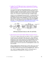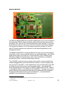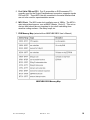
1
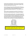
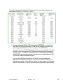
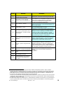
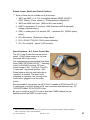
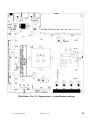
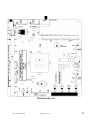
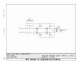
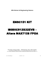
SFU School of Engineering Science
ENSC151 KIT
M68HC912B32EVB –
Altera MAX7128 FPGA
Fred Heep, George Austin - 2003 February, Rev. 2007 January
Thanks also to Craig Scratchley and Qingguo Li for suggestions, improvements and technical proofing.
Special thanks to Winfield Zhao for mega-hours of personal time invested in bringing the kit and docs up to BasicIO-V6.
FLH HC12-FPGA_Kit
2007.01.19 10:11
1
Contents
Introduction........................................................................................................................... 4
Kit History and Revision Levels ........................................................................................ 5
How do I determine my kit’s revision level? ................................................................ 6
Where can I get a schematic drawing for my kit revision? ....................................... 6
Why don’t connector pin numbers on Rev. 1 kits correspond with newer kits?.... 6
Other Stuff You Need to Know Before Using Your Kit .................................................. 7
Tips on ‘How to damage your kit… and more’ ........................................................... 7
General Comments & User Tips................................................................................... 8
FAQ’s .................................................................................................................................... 9
1. What is the BLASTER connector on the FPGA board for? ................................. 9
2. Why does LED1 on the FPGA board flash?........................................................... 9
3. I’ve attached my wall-wart (AC power adaptor) power connector to the FPGA
board J1, but nothing happens. .................................................................................... 9
4. The MAIN PWR LED (LED2) is quite dim. Is this normal? ................................. 9
5. My kit suddenly stopped working. What do I do? ................................................. 9
6. What is the 8-position DIP switch on the Rev.2 and newer kits for?................ 10
7. On Rev.2C and D FPGA boards there is single position DIP switch (DSW2)
and trimpot (R19) about half way up the left side of the PWB. What are these
for?................................................................................................................................... 11
8. What purpose does the Audio Adaptor PWB connected to P8 serve?............ 11
9. My ADC channel AN2 on Rev2C or D kit doesn’t work. I keep getting a fixed
result that doesn’t correspond to my input signal. Other available channels
function as expected..................................................................................................... 12
10. Each time I press the EVB reset button, my terminal window displays a
bunch of garbage characters. Why? ......................................................................... 12
11. How much power can my kit supply to external project hardware? ............... 12
12. How can I connect the HC12 EVB to computer with USB only? .................... 12
M68HC912B32EVB .......................................................................................................... 13
Configuration Mode Jumpers ...................................................................................... 14
Serial Port Connection ................................................................................................. 14
ADC Channel Restrictions ........................................................................................... 14
ADC voltage reference VRH ....................................................................................... 15
Port S bits PS0 and PS1 .............................................................................................. 16
MCU Clock ..................................................................................................................... 16
EVB Memory Map ......................................................................................................... 16
Programming the HC12’s 768 byte-erasable EEPROM ......................................... 17
FPGA Board....................................................................................................................... 19
Introduction..................................................................................................................... 19
FPGA Device ................................................................................................................. 19
BasicIO Code for the MAX7128 FPGA Device ........................................................ 20
Audio Adaptor ................................................................................................................ 20
LED1................................................................................................................................ 21
LCD Interface................................................................................................................. 21
Push Button Switches................................................................................................... 23
FLH HC12-FPGA_Kit
2007.01.19 10:11
2
Interrupt Sequencing Logic.......................................................................................... 24
ByteBlaster Input ........................................................................................................... 26
Default Jumper, Switch and Control Positions ......................................................... 27
Special Interface Connections – A.C. Power Control Box...................................... 27
Reference Information .................................................................................................. 28
151 Kit FPGA Board Revision History ........................................................................... 29
Technical Drawings........................................................................................................... 33
Schematic – Motorola EVB912B32 ............................................................................ 33
Schematic - FPGA Board (Rev. 1C) .......................................................................... 34
Parts Placement - FPGA Board (Rev. 2A) ................................................................ 35
Schematic – FPGA Board (Rev. 2A).......................................................................... 36
Parts Placement - FPGA Board (Rev 2A) ................................................................. 37
Schematic - FPGA Board (Rev. 2C) .......................................................................... 38
Parts Placement – FPGA Board (Rev. 2C and 2D)................................................. 39
Audio Adaptor Board .................................................................................................... 40
FLH HC12-FPGA_Kit
2007.01.19 10:11
3
Introduction
The development kit issued to you for ENSC151 was designed and assembled by
SFU Engineering Science specifically for this course.
Before it is handed out, each kit has undergone a comprehensive series of
carefully performed inspections and electrical tests to ensure that your group
receives a fully serviceable package.
In this document, you will find information specifically about your kit – the details
you won’t find elsewhere. The frequently asked questions (FAQs) are all
discussed - “How do I determine my kit’s revision level, and what’s the difference
between them?”, “What does the FPGA do?”, “How should I take care of my kit to
ensure I am not penalized for damage?”, “What do I do if my kit stops working?”,
“Are there any electrical constraints I need to worry about when planning my
project?” … and so on.
FLH HC12-FPGA_Kit
2007.01.19 10:11
4
The kit, pictured above1, consists of two interrelated sections. On the left is the
M68HC912B32 EVB (Evaluation Board) created by Motorola. This is the
microcontroller heart of the kit. Although we’ve installed a few connectors,
essentially this section is preserved in original OEM condition so that all applicable
Motorola documentation still applies2. The larger board on the right, called the
‘FPGA’ board is SFU’s design and is interlinked with ribbon jumpers between most
of the MCU’s I/O (input/output) ports. The FPGA/CPLD3 manages the I/O from the
EVB MCU, provides user access to some of these signals, bi-directionally routes
signals between the MCU and the 2x16 (2 line x 16 character) LCD (liquid Crystal
Display), as well as facilitating an external interrupt handling scheme to the MCU.
Kit History and Revision Levels
Since its inception in late 1997, this kit has proven itself as an excellent learning
tool for both the microcontroller unit (MCU) and non-volatile configurable logic
(FPGA – Field Programmable Gate Array). Both the MCU and FPGA are industry
workhorses that haven’t changed much. They continue to be well supported and
documented by their manufacturers and user groups.
While there are many varied microcontrollers available from other fine companies
such as Atmel, Microchip, Texas Instruments, National Semiconductor, Dallas
Semiconductor, Intel, Hitachi, etc., the School continues to support the Motorola
microcontroller family. In this way, you will be familiar with the general operation of
the parts, their coding syntax, and programming methods when progressing into
other courses employing similar devices. While diversification into other product
lines is generally good in many circumstances, maintaining a pool of in-house
expertise on these specialized components is difficult if the products supported are
too varied. Once you’ve mastered the use of all the HC12’s resources, which is
the primary goal of the ENSC151 course, you should be able to migrate to just
about any other MCU with confidence and relative ease.
While the EVB912 has pretty much stayed the same since the School started
using them, the FPGA board has changed a number of times. Each year that the
ENSC151 course is offered the enrolment has increased and so has the need for
more kits. As the course has evolved, through various instructors and many
different student projects, we have tried to incorporate a few new features (and
correct the odd bug) when constructing a new batch of boards.
Essentially, all revisions are electrically the same – tremendous confusion would
result if the core circuitry were different. However, kits introduced starting at Rev.
2A, have a few more user-friendly features. These include better connector
access - especially for power and I/O, power on/off switch, direct access to probe1
The FPGA board has evolved in a series of extended feature revisions. The image shown represents one of the latest
versions. (See Revision History for specific differences between kits).
2
Users of kits programmed with D-Bug12 V2.0A code should be aware that this version has been altered slightly by SFU.
3
In the early 1990’s, FPGA (Field Programmable Gate Array) was the conventional term given to this type of device. Since
then, the name CPLD (Complex Programmable Logic Device) has gained broader acceptance and is perhaps better
suited. For legacy and consistency interests, this document will continue to use FPGA.
FLH HC12-FPGA_Kit
2007.01.19 10:11
5
points for testing and calibrating the kit, wider range of LCD module acceptance
and LEDs for improved fault detection. For those interested, the step-by-step
revision history is included toward the end of this document; it explains, in detail,
exactly what is different about each revision level.
How do I determine my kit’s revision level? With the exception of the Rev.1 kits
that have no identification markings, all others (from Rev. 2 up) are clearly marked.
If you look at the FPGA board, to the left of the Altera FPGA chip, you will find a
white silkscreened title box containing “SFU ENGINEERING SCIENCE,
HC12/FPGA DEVELOPMENT SYSTEM, REV xx”. The ‘xx’ defines the revision
level.
Where can I get a schematic drawing for my kit revision? All kit and revision
specific documents are available at the end of this document as well as from the
course web site. Keep the schematic handy – you’ll likely refer to it frequently.
Why don’t the connector pin numbers on Rev. 1 kits correspond with newer kits?
One of the big headaches with the original Rev.1 kits was that the designer chose
to use a non-conventional connector pin-out numbering scheme. This led to mass
confusion that still continues. From Rev. 2 onward, this was corrected. If you look
at any of the kit schematics, you’ll see connectors diagrammed as shown here.
The numbers inside the box represent the conventional numbering sequence.
Numbers in brackets (x) correspond to the ident. markings silkscreened on Rev. 1
FPGA boards. They continue to appear on all drawings for legacy reference only.
Connector Pin Numbering
In all documentation and correspondence you generate, always refer to the
connector pin by the conventional number – those shown within the symbol
box. For example P1-5 denotes connector P1/pin 5. Use the (x) references
only when trying to physically locate a connector pin on a Rev. 1 kit.
FLH HC12-FPGA_Kit
2007.01.19 10:11
6
Other Stuff You Need to Know Before Using Your Kit
1. Tips on ‘How to damage your kit… and more’
But really… all joking aside, here’s a list of things you shouldn’t do to your
kit. Some are real ‘no-brainers’, but many happen each year.
¾ Handle electrical contacts before discharging your body of hazardous
static electrical charges to earth ground.
¾ Carelessly short I/O pins to ground, neighbouring pins, or +5V rail.
¾ Drive I/O pins with external signals that exceed the maximum electrical
specs for the HC12. In most cases this involves exceeding the +5V
power supply rail, or applying negative voltages below ground rail.
¾ Drive ADC inputs with signals exceeding +5V or below 0V.
¾ Set the ADC reference VRH to greater than +5V.
¾ Attempt to drive AC power control devices from the 117VAC line without
proper isolation.
¾ Make hardware modifications to your kit or connected external circuitry
while the kit is powered or operating.
¾ Make configuration changes to your kit or Project Daughterboard while
the kit is powered or operating.
¾ Program the MCU improperly, or attempt to reprogram FLASH memory
intended for use by the resident D-Bug12. To avoid potential problems when programming your code in miniIDE, use the F8 (download file)
button to initiate file transfer options.
¾ Reverse the EVB power leads.
¾ Connect the EVB power terminals to an outside power source exceeding
the EVB’s input voltage ratings. The EVB has no voltage regulator onboard.
¾ Trip over long cables suspended carelessly from your kit.
¾ Permit electrically conductive foreign objects to contact the circuitry of an
operating kit.
¾ Use a wall-wart or external power supply not approved for use with your
kit.
¾ Drop, run over, create large burn marks on, etc. (“Will that be cash or
cash?)
¾ Spill coffee, pop, etc. on your kit – (Sold! “Would you like us to bag it for
you?”)
¾ Leave your kit and/or accompanying parts unattended in an insecure
area. (Obvious – but happens all the time).
¾ Place indelible marks on the base or plexiglass covers or return the kit
with ‘dress-up’ materials incompletely cleaned-off. The School will be
pleased to share the misery of extra labour & materials expenses with
you.
FLH HC12-FPGA_Kit
2007.01.19 10:11
7
2. General Comments & User Tips
¾ If you lose your kit – report it immediately to your instructor by email with
as much circumstantial detail as you can provide. Be sure you know the
kit number and the name(s) of the borrowers.
¾ Many of the trimpots on your kit are for the calibration of critical functions
– these have been carefully set just prior to the kit being issued to you.
Unless you know exactly what you are doing – don’t get tweak-happy. If
there is a hole in the plexiglass lid to access an adjustment point, R6
(and R19 on R2C&D or newer), you may adjust these only once you
know exactly what they do and how to use them. Otherwise – PLEASE
don’t touch it!
¾ Please don’t use a pen to operate the EVB reset switch. Use a nonconductive item – the rounded end of a Chop-Stick works great.
¾ Screws for the plexiglass lids should delicately tightened. Overtightening can lead to a cracked lid for which you may become
financially liable. Ideally, plexiglass covers should only be removed by
the technical support staff for your course.
¾ Any additional cosmetic modifications you make to ‘dress-up’ your final
project must be completely removed before hand-in. This includes stuff
like paper, sticky tape, glue, extra mechanical accessories, coloured ink
marks and so on. We don’t want to fix, and you don’t want to pay – do
you?
¾ Rev. 1 kit power input access can be awkward for some people. Just
can’t get your fingers under the plexiglass cover??? Try this
FLH HC12-FPGA_Kit
2007.01.19 10:11
8
3. FAQ’s
¾ What is the BLASTER connector on the FPGA board for?
This connector allows a programming device called a ‘ByteBlaster’ to
connect the FPGA chip to a PC for programming purposes. Unless
you’re reprogramming the Altera chip, you don’t need to worry about
this input.
¾ Why does LED1 on the FPGA board flash?
The flashing LED lets us know that the Altera chip is (most likely)
functioning normally and that it contains the BasicIO code needed for
your assignments. The flash sequence and rate also lets the Lab
Staff know what version of BasicIO code is presently in the device.
As of January 2007, the BasicIO has been improved to version 6 –
now LED1 will flash for about 6 seconds on kit power up, then go out.
Once out, it can be accessed by the MCU (PortB-7) for code
experimentation.
¾ I’ve attached my wall-wart (AC power adaptor) power connector to the
FPGA board J1, but nothing happens.
First, make sure the wall-wart is plugged into a live AC receptacle. If
you’ve got a Rev.2 or newer kit, check the POWER switch directly to
the right of the BLASTER input connector P11. Right=Power ON. In
normal operation for all kits, MAIN PWR LED2 should be lit with good
brightness. If the switch isn’t applicable or doesn’t fix the problem,
check for shorting jumpers installed on JMP1 and JMP2 (beside the
power input jack – J1. Not applicable for Rev. 1). If these are
installed, and the kit still doesn’t work, please bring the kit and wallwart to the Lab Tech (ASB9856) for further assessment.
¾ The MAIN PWR LED (LED2) is quite dim. Is this normal?
No. This is likely an indication that something is wrong with the wallwart, or more likely, something on the kit is drawing too much current
– far more than it should be. Please bring the kit and wall-wart to the
Lab Tech (ASB9856) for further assessment.
¾ My kit suddenly stopped working. What do I do?
A. In virtually all cases when things suddenly stop working, the kit is
fine! You’ve more than likely created a bug in your code that
caused a stack overflow, failed to originate or initialize the MCU
properly, got stuck in a loop - there can be many possibilities4.
Did you instruct D-Bug12 to start executing from the defined
address (something like ‘>g 0800’)?
4
Based on past experience, these are a few of the more common faults. Depending on the code development software
tools you are using (ie. Codewarrior & HIWAVE) many pitfalls may be fairly easily averted.
FLH HC12-FPGA_Kit
2007.01.19 10:11
9
B. Always keep a reference piece of ‘known-working’ code handy to
test with –preferably in the compiled .S19 format5. Reprogram
the HC12 with the good code and run it. If it runs normally, you
know that you’ve goofed something in your current work.
C. When the kit is powered up, is the MAIN PWR LED2 lit? If not,
and you are using a Rev. 2 or newer kit, check the POWER slideswitch directly to the right of the BLASTER input connector P11.
Right=Power ON.
D. Ensure that the Terminal program you’re using is setup properly
for 9600 Baud, then reset the MCU. D-Bug12 should respond
properly with the text message “… D-Bug12 V2.1.0b15”. If this
doesn’t happen, remove the power from the kit, wait about five to
ten seconds before reconnecting the power. Press Reset again.
E. Check to ensure that the serial cable is properly connected to the
PC and your kit, the proper COM port is selected and configured
for 9600,8,1,N in the terminal program.
F. If none of these points gets things up and running again, please
bring your kit (complete with wall-wart, serial cable, and if
applicable, you Project Daughterboard) to your T.A. or Lab Tech
(ASB9856) for a more comprehensive assessment.
¾ What is the 8-position DIP switch on the Rev.2 and newer kits for?
Because FPGA-P8 is a SIL (Single In-Line) header intended for
connection of fixed hardware – like the Audio adaptor board, this created
access problems for Rev.1 kit users when tying on external project
hardware. Seeing this shortcoming, when we introduced the Rev.2
series kits, we allowed access to these precious FPGA I/O lines using a
more conventional and easy-to-use dual-row connector- P8A. However,
since P8A is essentially wired in parallel to P8, it’s important to disable
dedicated P8 connections from user access at P8A. Hence P8
PRIORITY selector DIP switch DSW1-(middle 4 positions)6 should be off
– these lines are used by the FPGA/PWM and audio board. Unless
there is other hardware connected to P8, all other DSW1 positions
should be ON.
5
Check the course website for LCD2002.S19. This is an ideal simple test that exercises both lines of the LCD with
constantly changing data. It originates at 0800.
6
DSW1 may be populated in 2 orientations. The orientation shown in the schematic is the reference (DSW1-1 is located
directly above the ‘DSW1’ label on the FPGA board).
FLH HC12-FPGA_Kit
2007.01.19 10:11
10
¾ On Rev.2C and D FPGA boards there is single position DIP switch
(DSW2) and trimpot (R19) about half way up the left side of the PWB.
What are these for?
You’ve got a new kit with a handy additional feature. If you check the
schematic for your Rev. 2C or 2D kit, and trace the AN2 signal, you’ll
find that it connects to DIP switch DSW2. In the C1 position, this SPDT
switch routes AN2 to the A/D connector FPGA-P4 (for outside world
inputs). Or, in C2 position, trimpot R19 becomes a variable voltage
source for you to measure and experiment with. If you haven’t had a lot
of experience with the ADC yet, you can write some test code using
ADC-AN2 and sample the user adjustable 0-5V input from trimpot R19.
With a DMM on testpoint TP7 and GND (there’s holes in the plexiglass
lid for this), you can measure the actual voltage applied to the MCU’s
AN2 input. C1 is the default mode; please make sure the switch rocker
is depressed at C1 when you’re not using this accessory option.
E
x
t
r
a
ADC Experimentation Features on Rev. 2C and 2D Kits
¾ What purpose does the Audio Adaptor PWB connected to P8 serve?
This is part of a legacy design and is provided on all kits for consistency.
It functions from two dedicated FPGA chip I/O pins. Earlier ENSC151
courses offerings concentrated on both assembly language and VHDL
programming. One of their exercises was to code the FPGA and HC12
to generate precision musical tones using the reference clocks, four
pushbutton switches (FPGA-S1 to S4), MCU interrupts and timers. Notto-worry though - you won’t need to be so knowledgeable in order to use
this connection.
With the implementation of BasicIO ver6 in January 2007 (core code for
the MAX7128 FPGA device), audio frequency tones generated by the
HC12 MCU PWM section can be sent to the headphone jack. Audio out
Left = PortP-3 and Audio out Right = PortP-2. A 2-circuit jumper is
required between FPGA Board P5-(1+2) and P8-(13+14).
FLH HC12-FPGA_Kit
2007.01.19 10:11
11
¾ My ADC channel AN2 on Rev2C or D kit doesn’t work. I keep getting a
fixed result that doesn’t correspond to my input signal. Other available
channels function as expected.
If you are using a Rev.1, Rev.2A or 2B kit, please bring this concern to
your TA or Lab Tech (ASB9856). For Rev. 2C or 2D kits, check DSW2
(single position DIP switch mid way up the FPGA board left side). The
rocker should be depressed on the C1 side (top).
¾ Each time I press the EVB reset button, my terminal window displays a
bunch of garbage characters. Why?
After pressing the EVB Reset button, the MCU’s D-Bug12 defaults to
9600 Baud communication mode. If your terminal program is not set for
9600 Baud as well, this error will result. This shouldn’t be a concern for
users of Metrowerks’ Codewarrior Hiwave.
¾ How much power can my kit supply to external project hardware?
First, and most important - unless it’s endorsed by your instructor, TA or
Lab Tech (ASB9856), don’t hook any additional circuitry to the kit’s +5V
power. Once you have documented your plans in an acceptable form,
and received the ‘blessing of approval’ from one of the technical lab staff
with a green light to proceed, please ensure that your external hardware
doesn’t draw any more than 25-50mA. For most applications this is
plenty, but if you need more (especially if you’re driving lots of LEDs), an
additional external power source may be required.
¾ How can I connect the HC12 to a computer with USB only?
To facilitate communications between the HC12EVB and a USB only
computer, such as a laptop, you will need a USB to Serial Converter
such as the ATEN UC-232 or similar. These are relatively easy-to-find,
inexpensive devices.
To use the converter, you will need
to install a software driver on your
computer. Windows O.S. will assign
a COM port ID number. You can
determine this by looking in the
Device Manager [Start->Control
Panel->System->Hardware->Device
Manager->Ports Com & LPT].
Most terminal programs that we’ve
tried have no problem
communicating with the EVB on any assigned COM port, however,
experiments with Code Warrior/HiWave have led us to conclude that
only COM ports within the range of 1 to 4 will work.
FLH HC12-FPGA_Kit
2007.01.19 10:11
12
M68HC912B32EVB
The Motorola 68HC912B32 microcontroller supplied with your kit is one member of
the much larger 68HC12 family containing many variations of this microcontroller
unit (MCU) core. Both the HC12 and its predecessor, the 8 bit 68HC11 (still used
by the School) continue to be some of the most successful controllers in industry.
The automotive industry is one of the largest consumers and many of the HC11
and HC12 family members are customized to fulfill specific applications in the
transportation sector.
The M68HC912B32 EVB is somewhat different from most of its low-cost category
competitors in that it comes complete with its own resident Debugger. Most others
need special support tools such as In-Circuit Emulators (ICE) to efficiently and
effectively manage the development process, have cumbersome or expensive
programming issues, or have a limited support network.
The HC912B32, apart from being a feature-rich controller, comes complete with
resident Debugger and serial communications interface to transfer program code
from a host PC to the MCU. In the simplest terms, all you really need is a PC with
a standard 9 pin D-sub serial port and a terminal program – such as MiniIDE –
freely downloadable from the Internet or IAMS12 supplied with the EVB. IASM12
is copyrighted software, not available for free distribution7. However, more recent
course offerings are pursuing more elaborate and sophisticated IDE (Integrated
Development Environment) tools such as Codewarrior – a special edition is
available for free download from Metrowerks.com.
7
Students wishing to use the IAMS12 software are welcome to ask their instructor for a copy for use during the ENSC151
semester only.
FLH HC12-FPGA_Kit
2007.01.19 10:11
13
There are however a few EVB912 technical limitations and user restrictions that
you need to be aware of. These are not easily found in other documents.
1. Configuration Mode Jumpers. Before using your EVB, please check to
ensure that all jumpers are configured for normal operating mode. There
should be no reason for you to deviate from these settings. All 3-pin
jumpers W3, W4 and W7 should be installed on the inside pins (closest to
the P3 side).
2. Serial Port Connection. Motorola recommends that your EVB be powered
before connecting the serial cable to the EVB. This is a known weakness in
their design often resulting in damage to the MAX562 serial interface chip.
While we have not experienced significant problems in this regard, perhaps
due to the EVB interconnection within our kit, we strongly urge you to follow
this practice especially because most of you are interconnecting with widely
differing computer hardware.
3. ADC Channel Restrictions8. Unless you’ve been specifically authorized
by your instructor, do not use ADC Channels AN0, AN1 or AN7. AN7 is
reserved for SFU ENSC Project Daughterboards. On Rev. 2C and 2D kits,
JMP3 and JMP4 disable access to FPGA-P4 signals AN0 and AN1.
AN0 and AN1 serve a dual purpose. They are tied in with the EVB
operating mode configuration circuitry, making these two channels more
difficult to use. In the following illustration, you’ll notice that, in normal
operating mode, jumpers W3 and W4 pull these two AN lines to ground
through 15K resistors R7 and R8. Because of these two resistors, any input
voltages applied to AN0 or AN1 will be electrically influenced by R7 and R8.
If you drive these inputs with a 5V rail-rail op-amp output, the 15K resistors
probably won’t make a big difference. But if you’re trying to measure a
more sensitive higher impedance source – you’ll go nuts trying to figure out
why your ADC readings are so grossly out-of-line with expectations. Too
many students have blown these channels out because they didn’t take the
time to study or understand these implications. The full EVB912 schematic
is given toward the end of this document.
8
Some extra features have been added to Rev. 2C and 2D kits to permit easier experimentation with the ADC. Please
also refer to the FAQ section 3 “On Rev.2C and D FPGA boards there is single position DIP switch (DSW2) and trimpot
(R19) about half way up the left side of the PWB. What are these for?”
FLH HC12-FPGA_Kit
2007.01.19 10:11
14
Simplified Drawing of EVB912 ADC
Channels AN0 & AN1
4. ADC voltage reference VRH. For both experimenter damage protection
and to provide a cleaner reference voltage for the Analog to Digital
Converter (ADC), the EVB uses a 1K series resistor from the main +5V rail
to the MCU’s VRH input pin. A 10uF capacitor decouples any unwanted
supply noise from the VRH pin to ground. See diagram ADC VRH & VRL
Connections - illustration A.
This little feature can present both desired and undesired properties. A
primary advantage can be gained by allowing the user control the ADC
reference voltage impressed on the MCU’s VRH pin to a voltage lower that
the +5V supply. This can be done simply by adding an external fixed
resistor between VRH and ground to form a voltage divider between EVB
R1 and R-YOURS as pictured in illustration B. Thus, you can scale the
ADC’s sensitivity range to suit the magnitude range of the signals to be
sampled from the outside world. On the down side, it’s very important to
remember that any current drawn on this line will cause a voltage drop
across EVB-R1 which can significantly influence your measurements.
ADC VRH & VRL Connections
FLH HC12-FPGA_Kit
2007.01.19 10:11
15
5. Port S bits PS0 and PS1. Port S, accessible on EVB connector P3 normally used for the Project Daughterboard connection, supports signals
PS0 and PS1. These MCU bits are committed to the serial interface and
are not to be used for experimentation access.
6. MCU Clock. The MCU main clock oscillator runs at 16MHz. The MCU’s
main internal bus however, runs at 8MHZ (Master_Clock÷2). This not-soobvious tidbit should be very important to you when calculating timesensitive coding routines – like delay loops, etc.
7. EVB Memory Map (extracted from M68EVB912B32 User’s Manual)
M68EVB912B32 Memory Map
FLH HC12-FPGA_Kit
2007.01.19 10:11
16
The table below lists the default HC12 Interrupt Vector and Jump addresses as
structured in D-Bug12 (V2.0.A & V2.1.0b15).
8. Programming the HC12’s 768 byte-erasable EEPROM is a bit different
than using the 256 bit RAM space. RAM can be loaded at relatively high
speeds (typically 9600 baud or faster), whereas the EEPROM is
comparatively slow. HI-WAVE manages this for you automatically, but many
terminal or less sophisticated IDE (Integrated Development Environment)
programs don’t. To achieve a successful load to both RAM and EEPROM
with MiniIDE, communications baud rate needs to be dropped down to 600
on both the EVB and terminal program.
If you’re using MGTech’s MiniIDE or HI-WAVE (a utility bundled with
Metrowerks CodeWarrior for HC12) as the communications software, use
this table as a guide. Other IDEs are similar, but may need a bit of tinkering
with the user interface to set the communications parameters appropriately.
FLH HC12-FPGA_Kit
2007.01.19 10:11
17
STEP
1
Power up Kit. Connect HC12 to
computer using the serial cable.
2
Start MiniIDE. From the Windows
Desktop, double-click the MiniIDE icon.
3
View -> Window -> Terminal
4
Terminal -> Options -> Terminal. Check
Com(X), 9600, 8, 1, none
Top menu bar; D-Bug12 -> Set MCU Type. In the dialog
box, select MC68HC912B32. Click OK.
5
Place cursor in terminal window. Press
HC12 reset button. The D-Bug message
should appear.
If HIWAVE can’t automatically establish communications
with the HC12, you may get an error message leading to a
dialog box in which to adjust the communications settings.
12
Typically you should use 9600 baud rate and COM1,
unless your system is configured differently. Alternately you
can change the Communication Device Specification in HIWAVE by selecting D-Bug12 ->Communication.
6
At the > prompt, type baud 600 & press
RETURN.
Top menu bar; D-Bug12->Connect->Communications
13
Device->check Show Protocol . Press HC12 reset button.
Motorola’s D-Bug12 initialization ID sent by the EVB912
should come up in the HI-WAVE Command screen.
7
Terminal -> Options. Change baud rate
to 600.
Top menu bar; File -> Load Application. In the resulting
‘Load Executable File’ dialog box, set the File Type = *.s?*.
(Default = Load Options -> Load Code + Symbols). Set
Code Verification Options -> None. Locate the directory in
which your desired S19 program file resides and select the
file. Click Open. This loads your file into the HC12.
8
Set cursor back to terminal window. Type
LOAD at the > prompt & press RETURN.
9
Press F8 to select your S19 program file.
OPEN.
10
11
9
10
11
12
13
HI-WAVE 9,10,11
MiniIDE
Power up Kit. Connect HC12 to PC using the serial cable.
Start HI-WAVE. From the Windows Desktop, double-click
the HI-WAVE icon (or in CodeWarrior’s program folder, find
Hiwave.exe in the Prog subdirectory). (HI-WAVE is a
subcomponent bundled with the CodeWarrior HC12
program as downloaded from Metrowerks).
Top menu bar; Component -> Set Target. In the resulting
dialog box set Processor = HC12 and Target Interface = DBug12 Target Interface.
In the Command window, type g $ + your program’s start
address, return. The HC12 should now execute your
program.
eg. g $0800 ↵
The terminal window indicates the file
being uploaded to the HC12.
On completion of load, the > prompt
should be displayed. Type g (space) &
start address of your program code
eg. g 0800 ↵
Code Warrior steps 3-5 are preconfigured (project.ini file) on ENSC undergrad lab computers. Step 6 is optional.
On ENSC lab computers TEK VISA software can prevent Code Warrior from establishing communications with the EVB.
Close Code Warrior. Locate TEK VISA icon on the lower right system tray, right click and Close. Restart Code Warrior.
USB->RS232 converters. Our findings indicate that Code Warrior will only function on COM1-4. In Windows OS, you
may need to confirm USB port assignment settings in the Device Manager.
On Power-Up or manual Reset, the EVB will always default to 9600 baud. HI-WAVE may attempt to shift communications
to 38400 baud. Both the EVB and the terminal program must be set for the same baud rate. Step 6 should help identify
discrepancies if communication is lost.
The Show Protocol step is not normally required. HI-WAVE attempts to establish communication on the preset COM port
by scanning standard baud rates. This feature may be useful in confirming that the EVB912 is communicating properly.
FLH HC12-FPGA_Kit
2007.01.19 10:11
18
FPGA Board
Introduction
The Motorola HC12 evaluation kit is interfaced with a second PWB (Printed Wiring
Board) that contains an Altera FPGA/CPLD14 chip (MAX EPM7128SLC84C-7) and
a 2 line x 16 character LCD display. Also included on the FPGA board are four
push button switches and some clock generating circuitry that may be used to
generate audio tones and other logic timing functions within the FPGA.
In its infancy, the ENSC151 course included introductory instruction on VHDL
programming for the FPGA as well as teaching assembly language coding for the
HC12 microcontroller. For a variety of reasons, teaching both devices was
unmanageable for both the staff (especially as class sizes grew), and a
tremendous amount of work for the students and T.A.s. Hence, the current course
focus is on the microcontroller – which has more than plenty of stuff to explore and
learn about. We have programmed the FPGA with a BasicIO code that provides
some signal routing, buffering and isolation between the HC12 EVB and other kit
support circuitry and external connections. This provides some limited protection
for inexperienced users who might try to connect inappropriate circuitry to their kit,
potentially frying the HC12.
Some explanation of each of the several sub systems is required to appreciate just
what is connected to the HC12 and how it works.
FPGA Device
The FPGA device (Field Programmable Gate Array) can be thought of as a
collection of configurable hardware circuit elements (logic gates, flip-flops,
counters, buffers, and so on) that can be inter-connected using a logic definition
code that compiles into a form that can be “programmed” into the FPGA device.
For now it is not important to understand how this interconnection is achieved, only
that the logic function that the user requires can be defined by using a high level
programming language called VHDL (Very High Speed Integrated Circuit
Hardware Description Language). Within the VHDL programming language, the
user can define the logic function that must exist between various input and output
pins of the FPGA device. In this way, a very complex, customized series of logic
elements can be configured in a physically small package by programming the
FPGA device. For the present purposes of the ENSC151 course (we are no
longer teaching an FPGA programming component), you may consider the kit’s
FPGA as a protection device – limiting potential electrical damage from occurring
14
In the early 1990’s, FPGA (Field Programmable Gate Array) was the conventional term given to this type of
device. Since then, the names CPLD (Complex Programmable Logic Device) and EPLD (Electrically Programmable
Logic Device) have gained broader acceptance and are perhaps better suited. For legacy and consistency interests, this
document will continue to use the term ‘FPGA’.
FLH HC12-FPGA_Kit
2007.01.19 10:11
19
to the difficult-to-replace HC12, but also to add some customizable functionality to
each of the kits.
BasicIO Code for the MAX7128 FPGA Device
In order to establish the electrical signal routing and other special features the
FPGA provides, it must first be programmed. This is not something you need to
worry about doing. The Lab’s technical staff perform the service of installing the
BasicIO code for this part during the comprehensive testing process the kit goes
through before it is issued to you.
When you power-up your kit, the BasicIO code in the FPGA will flash LED1, letting
us know that the Altera chip is (most likely) functioning normally and that it
contains the BasicIO code needed for your assignments. The flash sequence and
rate identifies the BasicIO code version presently in the device.
As of January 2007, the BasicIO has been improved to version 6 – on kit power up
LED1 will flash at about 5Hz/75% duty cycle for about 6 seconds then goes out.
Once extinguished, the FPGA releases control for LED1 to the HC12 MCU so that
it may be utilized for code experimentation.
Audio Adaptor
As discussed in the preceding FPGA BasicIO Code sub-section, the Audio Adaptor
can now be used with BasicIO Ver6 (or newer) to permit monitoring of audio
signals generated by the HC12 MCU. HC12 PWM (Pulse Width Modulation)
Signals PP2 and PP315 will be routed to the Audio Adaptor16. This feature will
permit you to experiment with PWM programming. Components on the Audio
Adaptor board help to filter and smooth the ‘raw’ sounding digital signals to
something more acceptable to the ears.
Audio Adaptor
Board
Schematic
15
Many of the MCU pins can be configured (by your code) to perform multiple functions. In this case, Port P-(P0-P3) can
be used for general I/O or as Pulse Width Modulation (PWM) outputs. See HC12 Data Sheet or Technical Summary for
block diagram or pin assignments.
16
A 2-circuit jumper is required between FPGA Board P5-(1+2) and P8-(13+14).
FLH HC12-FPGA_Kit
2007.01.19 10:11
20
LED1
LED1, located near the lower left corner of the MAX7128 FPGA chip, serves a dual
purpose. Most importantly, upon power-up, it provides an immediate visual
reference to the user confirming the code version contained in the FPGA. BasicIO
Ver6 or newer (January 2007) will flash LED1 at 5Hz/75% duty cycle for about 6
seconds on power-up, then goes out. Once extinguished, the FPGA releases
control for LED1 to the HC12 MCU so that it may be utilized for code
experimentation. LED1 is controlled by PORTB bit 7 (active high).
LCD (Liquid Crystal Display) Interface
From a programmer’s point of view, the LCD interface consists of an 8-bit parallel
interface supplied from all eight bits from Port A of the HC12. In addition, there are
three extra control lines required to control the LCD, namely, LCD RS (Register
Select), LCD R/W (Read/Write) and LCD E (Enable or Strobe) and these three
lines come from Port B bits PB6, PB5 and PB4 respectively. An LCD is mostly an
output device, but there are functions concerning the control of the device that
force it into an input mode (reading the busy flag, reading the character address,
etc.). This input mode complicates the role that the FPGA plays in this interface.
With the implementation of BasicIO Ver6 (January 2006), it is now possible to poll
the LCD status flag to determine if the LCD is busy or ready to accept another
instruction. This is implemented by means of signal HC12-PE2 check_LCD_busy.
When this signal is set (logic 1), the FPGA will read the LCD busy line and if the
LCD is busy (busy flag is low), the FPGA will generate an interrupt to the HC12.
(See the Interrupt section of this document). Important: For normal LCD
operation, you must set check_LCD_busy signal as logic low.
Remember, one of the original intentions of this FPGA application, was to help
shield the HC12 from poorly designed interface circuits (from well meaning
students) so if students do clobber the system, hopefully the device destroyed is
the FPGA and not the HC12. This doesn’t imply however that recklessly
interfacing to external hardware is OK – be very careful!. While the FPGA chip can
be replaced relatively easily – it is a complex and expensive component (2007Jan
- $75CDN to replace). To provide this isolation between the HC12 and the outside
world, we simply add buffer elements (in the FPGA) on each signal line to and
from the HC12. The resulting circuit would look something like this
FLH HC12-FPGA_Kit
2007.01.19 10:11
21
Buffer Elements within the FPGA provide Isolation
When we require that the 8-bit data bus for the LCD be bi-directional, this adds
some complexities to the FPGA function, now we must specifically enable the
direction of data flow through the buffers. Here’s a typical bi-directional buffer
circuit.
Equivalent Circuit of FPGA Internal Bi-Directional Buffer
Obviously, to achieve bi-directional buffered signals without the direction control,
we would be connecting two buffers back to back creating a simple latch (which
does not achieve what we want to do)! The output control enables the buffer gates
in the desired direction by controlling the output enable on each buffer. For the
LCD interface, we have eight bi-directional lines (port A bits PA0 to PA7) and three
control lines from port B - bits PB4, PB5, and PB6. One of the control lines (LCD
R/W) is the read/write control for the LCD and it can be used as the directional
control. When LCD R/W = 1 we read from the LCD and when it is equal to 0, we
can write to the LCD.
FLH HC12-FPGA_Kit
2007.01.19 10:11
22
HC12 <> FPGA <> LCD Interface
HC12
Signal
Port A bit 0
Port A bit 1
Port A bit 2
Port A bit 3
Port A bit 4
Port A bit 5
Port A bit 6
Port A bit 7
Port B bit 4
Port B bit 5
Port B bit 6
HC12
Connector
P4 pin 19
P4 pin 20
P2 pin 1
P2 pin 2
P2 pin 3
P2 pin 4
P2 pin 5
P2 pin 6
P4 pin 2
P4 pin 3
P4 pin 4
FPGA
Input
Pin
15
16
11
12
9
10
6
8
33
31
30
FPGA
Output
Pin
73
74
75
76
77
79
80
81
70
69
68
LCD signal
LCD
Connector
LCD bit 0
LCD bit 1
LCD bit 2
LCD bit 3
LCD bit 4
LCD bit 5
LCD bit 6
LCD bit 7
LCD E
LCD R/W
LCD RS
P6 pin 7
P6 pin 8
P6 pin 9
P6 pin 10
P6 pin 11
P6 pin 12
P6 pin 13
P6 pin 14
P6 pin 6
P6 pin 5
P6 pin 4
Note that the port B signals on bits 4, 5 and 6 are uni-directional output signals and
can be implemented with the simple buffer circuit shown earlier in this document.
The Port B bit 5 signal (LCD R/W) is used as the directional control line in the bidirectional buffer.
With the implementation of BasicIO-V6 (Jan. 2007), you can read the FPGA code
version code from PortA when LCD-RS and LCD-R/W signals are high and LCD-E
is low. The version number is read simply as a binary number and is the HEX ($)
coding of the version number. For example Version 6.0 = 1100000, Version 6.1 =
01100001, etc.
Push Button Switches
The 4 push button switches that are implemented on the FPGA PCB are simply
tied back to bits 0, 1, 2, and 3 of port B (via the FPGA as a non-inverting buffer
similar to that described in the LCD subsection). Activation of any of the four
switches will send an active low signal to the respective HC12 port B pin in
accordance with the following table.
FPGA BOARD PUSHBUTTON SWITCH ASSIGNMENT
FPGA PWB
FPGA
FPGA
HC12
HC12
Signal Name
Input pin Output pin Connector
Signal
[SW1] S1 yellow
51
36
P6 pin 18
Port B bit 0
[SW2] S2 red/Orange
50
34
P6 pin 19
Port B bit 1
[SW3] S3 white/Grey
49
35
P6 pin 20
Port B bit 2
[SW4] S4 blue
48
31
P4 pin 1
Port B bit 3
FLH HC12-FPGA_Kit
2007.01.19 10:11
23
Interrupt Sequencing Logic
Controlling external devices using the HC12’s interrupt input requires some
additional “Interrupt Sequencing Logic”. The purpose of this extra circuitry is to
synchronize an asynchronous event in the outside world with the very synchronous
environment of the micro-controller. To do this we require the use of a flip-flop that
is set (on a rising edge or falling edge from an external signal in our external
device). Once this flip-flop is set, it triggers an interrupt request in the HC12.
During the execution of the interrupt service routine (ISR - a sequence of
instructions in your code), the HC12 can check the status of this flip-flop to identify
the source of the interrupt and when the servicing of the interrupt is complete, the
flip-flop can be reset by the MCU. The following diagram illustrates the typical
interrupt sequencing logic employed in BasicIO-Ver.6.
Equivalent Circuit of FPGA External Interrupt Management Scheme
(BasicIO-Ver6
Normally, this interrupt sequencing logic would be implemented with discrete logic
on the PWB along with the external devices. In our case, the HC12 FPGA board
was already built, so we implemented the interrupt logic in the FPGA (aka CPLD –
Complex Programmable Logic Device).
Notice that the logic shown in the diagram will handle three “external” devices; the
LCD module, FPGA board pushbutton switches, and external interrupts generated
FLH HC12-FPGA_Kit
2007.01.19 10:11
24
by our project daughterboards. These are all managed by a series of flip-flops set
by the requesting device and cleared by the MCU. A wide 5-input NOR gate
permits all of the individual F-F’s to flag the single XIRQ signal input line to the
MCU.
Because the MCU has only one XIRQ line and we employ multiple devices that
can trigger an interrupt, we need to be able to determine which device caused the
event; the pushbuttons, LCD, or daughterboard. When the MCU receives an
interrupt on /IRQ(PE1), your ISR will need to sequentially poll the actual device
input pins. For the pushbutton switches, test PB0-PB3, LCD = PE3, and
daughterboard/GIO19 = PE5. Upon determining which device caused the
interrupt, the FPGA’s internal logic must be reset to permit the detection of the next
event. Apply a high-low-high (1-0-1) transition to the desired /RST line. HC12PE6 controls the reset for the pushbuttons and LCD, and HC12-PE7 for the GIO19
project daughterboard. Observe that /RST1 (PE6) will only clear the interrupt FF’s, but it won’t clear the LCD_Status; you’ll need to do this by clearing (low)
Check_LCD.
BasicIO-Ver.6 has significantly enhanced the LCD control options. The addition of
Check_LCD_Busy now permits the HC12 to solicit an interrupt when the LCD is
busy. When Check_LCD_Busy (HC12-PE2) is set (logic 1), the FPGA will read
the LCD’s busy flag and generate an interrupt if the LCD is busy (LCD Busy Flag =
0). For normal LCD operation, Check_LCD_Busy must low. The internal F-F
controlling the LCD busy flag is clocked from a relatively slow 200kHz source
derived from the MCU’s main clock. This was important for the successful
operation with various LCD modules. Some of the newer LCD models were
content at 2MHz.
Each of the four FPGA pushbutton switches is handled by a pair of flip-flops (S1’s
logic is shown at the top-centre of the diagram – the rest of the switches employ
the same logic but isn’t show for simplicity). One F-F handles rising edges and the
other falling. Whenever a PB switch is activated, an interrupt will be generated.
With this logic configuration we can realize some advantages. For example, if S1
is pressed and held, one interrupt will be generated. If, while S1 is pressed, S2 is
also pressed, another interrupt will be produced. Similarly, if S1 is released while
S2 is still depressed, the MCU will get another interrupt.
Finally, the external GIO19 interrupt handling for our project daughterboards is
structured around an independent a flip-flop triggered by any positive edge applied
to the GI/O19 pin from an external source i.e. an HC12 project daughterboard (pin
#5 on the FPGA device). The interrupt management equivalent circuit diagram is
simply a schematic representation of what we have implemented in VHDL source
code. For completeness, the VHDL code that defines the device #1 interrupt for
one switch is shown below.
FLH HC12-FPGA_Kit
2007.01.19 10:11
25
ENTITY sw_irq IS
port
(
sw, rst
status
);
END sw_irq;
: IN
STD_LOGIC;
: OUT STD_LOGIC
ARCHITECTURE a OF sw_irq IS
SIGNAL dl, d2
:
STD_LOGIC;
BEGIN
devicel_a: PROCESS (sw, rst)
— detect pressing switches
BEGIN
IF (rst = '0') THEN
dl <= '0';
ELSIF (sw'event AND sw = ‘1’) THEN
d1<= ‘1’;
END IF;
END PROCESS devicel_a;
devicel_b: PROCESS (sw, rst) - detect releasing switches
BEGIN
IF (rst = '0') THEN
d2 <= '0';
ELSIF (sw'event AND sw = '0') THEN
d2 <= ‘1’;
END IF;
END PROCESS devicel_b;
status <= ‘1’ WHEN (dl =’1’ OR d2 ='1') ELSE '0';
END a;
A note regarding the use of External Interrupts – Depending upon your
application, some students have run into weird behaviour issues with code
execution that isn’t obvious to fix. One such issue is the management of external
interrupts on the MCU. As a good practice, right at the top end of your code,
disable XIRQ. You may re-enable it later on as needed. Your instructor or TA
should be able to provide guidance.
ByteBlaster Input
To program the FPGA chip an Altera Byteblaster (or similar device) is used to
condition the data and control signals from the PC’s parallel port under the control
of Altera’s MAX Plus II development and programming software. This device
connects between the Kit’s ‘BLASTER’ connector (2x5 pin header) on the FPGA
board and the PC parallel port. To prevent accidental damage to your kit, we
recommend that the kit be powered before connecting the ByteBlaster. This is
because the PC parallel port can source a reasonable amount of power that, under
certain conditions, may have adverse effects on the MAX EPM7128 FPGA chip.
FLH HC12-FPGA_Kit
2007.01.19 10:11
26
Default Jumper, Switch and Control Positions
*** Some of these are not available on all kit revisions.
1. JMP1 and JMP2 = 1+2, 3+4 for supplied wall-wart MODE 68-650P-1,
6VDC, 500mA, 2.1mm, centre (+). [Power polarity configuration]
2. JMP3 and JMP4 both open. [AN0 and AN1 user enable]
3. DSW2 = depressed in C1 position. [AN2 External user/R19 adjustable
voltage reference trimpot]
4. DSW1 = middle group of 4 switches OFF – remainder ON. [P8/P8A priority
select]
5. R6 = Mid rotation. [Reference voltage adjust]
6. R15 = DO NOT TOUCH! [10KHz clock calibration]
7. R5 = Do not adjust – preset! [LCD contrast]
Special Interface – A.C. Power Control Box
The A.C. Power Control Box can be used to
switch 115VAC mains power to a <8A max
load under MCU logic control.
This unit employs an opto-isolated Solid State
Relay (SSR) [OPTO22 #120D10]17. Switching
occurs on the 0VAC crossing. DC input
control voltage 3-30V. Turn On & Turn-Off =
½ cycle max. Logic/Load isolation = 4KV.
Please observe that only one load outlet is
“switched” as marked. The other Fixed
receptacle is constantly “live” as long as the
control box is plugged into a live power
source.
Recommended kit connections use HC12 Port P available at FPGA board P5-1 &
2 (vertical pair or end pins closest to P8. Insert connector with black wire up). P51=PW3/PP3=Black, P5-2=PW2/PP2=Red.
Be sure to configure your HC12 code so that these PWEN channel bits are
disabled and set the DDRP to output mode.
17
Refer to the device datasheet for full specs. Info may be found on Lab computers, Desktop -> Reference Materials
folder -> Parts Data -> Opto -> Solid State Relay.
FLH HC12-FPGA_Kit
2007.01.19 10:11
27
Reference Information
The references listed herein should be available directly from your ENSC course
website. Alternately, use a good WEB search engine to locate them.
1.
2.
3.
4.
5.
6.
7.
8.
EVB912 User manual [ 68EVB912B32UM.pdf ]
EVB912 Information Guide [ M68EVB912B32.pdf ]
68HC12 Technical Summary [ M68HC12B/D.pdf ]
68HC12 Family Technical Reference Manual [ M68HC12B.pdf ]
Callable Routines in D-Bug12 [ AN1280A/D.pdf ]
HC12 Reference Guide [ CPU12RG/D.pdf ]
CPU12 Reference Manual [ CPU12RM.pdf ]
EVB912 Schematics [ MC68HC912B32EVBSCHEM.pdf ]
At the time of this writing, Motorola has listed many application notes and
documentation for the HC12 MCU. Please visit http://www.freescale.com/ 18 and
Part # Search for ‘68HC912B32’, ‘MC68HC912B32CFU8’, or Keyword Search for
‘68HC912B32 Product Summary’.
18
Freescale Semiconductor became an independent publicly traded company in July 2004 after more than 50 years as
part of Motorola, Inc.
FLH HC12-FPGA_Kit
2007.01.19 10:11
28
151 Kit FPGA Board
Revision History
Fred Heep
SFU Engineering Science
2007Jan
All kits updated to BasicIO-V6. Added 2 wire jumper between P5-1+2 and P8-13+14. This facilitates HC12
PWM output through MAX7128 to headphone jack on audio daughter-board.
Rev.1 to Rev. 2
August 1997. Patrick Leung created the original design of the FPGA board and schematic. There are no identification
markings on this version to identify it. This is considered the Rev.1 version. This design was done with relative urgency with
a new software package which Patrick was just learning. Some debugging was necessary to get this version operational.
1) Mount for LCD module not included. Needed custom wood support block.
2) Signals improperly routed & required manual patching as follows. Note, all pin ID's are as per original marked numbering
sequence.
a) Cut top P2-16 to U2-22. Patch P2-6 to U2-22. (ECLK)
b) Cut bottom P3-5 to P5-4. Jumper P5-4 to P3-6. (IOC2)
c) Cut top P3-16
d) Cut top P3-2
e) Patch U2-36 to P3-12
f) Patch P5-11 to P3-15. (IOC3)
g) Patch P11-7 to +5V
h) Install resistor 300R SMD0805 between P11-6 & P11-1.
j) Install capacitor 18pF between P11-6 & P11-1.
3) Board design & fab was not optimal for hand assembly & made construction difficult esp. for inexperienced assemblers.
4) Header pins do not follow industry standard numbering convention. This caused much confusion.
5) Location of A/D expansion connector P4 had to cross the voltage regulator. This is awkward and regulator
heating/convection cooling is obstructed and could cause damage to ribbon cable.
6) No polarization for P4 to ensure correct connector orientation.
7) No ident. function labeling on user accessible connectors.
8) P8 was difficult for students to connect to, especially if the audio board is in place.
9) Power connector P10 is difficult to access when the kit is assembled with its baseboard & plexiglass cover.
10) Power connection (+5V) from FPGA board to EVB uses a terminal block. Orientation was not optimized and therefore
wires were easily disturbed, broken or became intermittent.
11) Mounting holes for EVB to FPGA board had traces routed too close. Special care was needed in assembly and choice
of fasteners.
12) P7 is located under the LCD display unit making access difficult. Labelling is also on the inside making identification
difficult. Students needed to connect ribbon cable to this pin set and needed a dual row header.
13) Byte Blaster input P11 is too close under LCD unit making connection difficult.
14) In general, connector placement and style makes external access tough especially with plexiglass lid installed.
15) No Power switch.
16) 2002Dec - Inserted FB1 & FB2 into GIO18 & 19 lines by cutting traces directly opposite upper EVB mounting hole.
17) 2002Dec - Updated Schematic to FPGA-Rev1C.
FLH HC12-FPGA_Kit
2007.01.19 10:11
29
Rev.1 to Rev.2 (FLH 1099-01)
(October 1999)
Only one board of this revision (Rev.2) was populated as a trial.
1) Moved P4 (A/D), P11 (Blaster), J1 (power in), and P5 to outside edges using right-angle box connectors for easier access
& ensuring correct connector insertion polarity.
2) Added connector P7A dual row right angle box header to right board edge. This parallels P7 SIL header under LCD
module. Original P7 position retained for compatibility.
3) Added connector P8A dual row right angle box header to right board edge. This parallels P8 Utility Module SIL header at
bottom of board through newly added selector DIP switch DSW1. Original P8 position retained for compatibility with
expansion utility modules.
4) Added Test Points TP1 to TP6 to allow more convenient testing, trouble shooting and alignment.
5) Added HD1 and HD2 SIL headers to permit access/testing of unused HC912 connections from P2 and P3.
6) Created a new schematic.
7) Added JMP1 & JMP2 to permit (+) or (-) wall-wart power polarity configuration.
8) Added options for MTA100-2 locking header or 2 circuit terminal block for EVB912 power interconnect and changed
location.
9) Moved location of R15 multi-turn trimpot for CLK-HI to more convenient location.
10) Added provisions for C12 and R16 at byteblaster input.
11) Improved trace spacing around mounting holes.
12) Added function ident. labels to connectors and controls.
13) Added PWB identification label.
14) Corrected connector signal routing problems encountered in Rev.1
15) 2005 Jan – Added 10K termination resistors to GI/O18 and GI/O19 on FPGA board.
Rev.2 to Rev.2A (HC12/FPGA Development System REV 2A FLH 1099-01)
(1999 October)
1) Added LED3 to indicate EVB powered. Sometimes power connections between EVB and FPGA board become
intermittent so this feature was added to alert user to problems.
2) Added stand-off mounting hole for LCD module.
3) Added Power switch.
4) Added spare spacer pin between TP3 and TP4 to help prevent accidental short circuits on power supply.
Rev.2A to Rev.2B
(2002 October)
1) Added 2 more SIL headers, P6A and P6B above the original P6. These are flipped orientation (pin 1 left). This was done
to accommodate various other standard display modules.
2) Added more mounting holes for the LCD.
3) Added DSW2 DPDT, and R19 trimpot to ADC channel AN2. This combination will permit the user to experiment with the
ADC operation on AN2 using R19 as a variable voltage source. The dipswitch selects AN2 to be routed to P4 or R19.
4) Added JMP3 and JMP4 to disable P4 access to ADC channels AN0 and AN1 that serve multiple purposes on the EVB.
This has lead to student confusion and misunderstandings often resulting in blown HC912's.
FLH HC12-FPGA_Kit
2007.01.19 10:11
30
Rev.2A to Rev.2B
(2002 October)
1) P6A & P6B added to facilitate easier, more flexible, LCD display selection.
Now suitable for Tianma TM162ADA7-2 (RP Electronics) or Fema Electronics CM162L0-SGR1.
2) Additional LCD mounting holes added.
3) LCD contrast adj. Fixed resistor added and pot value changed. Pot position moved to accommodate difference display
installations.
4) Reduced proto area hole area to accommodate P6A, P6B and LCD mounting. Pads changed to Drill 40mils.
5) GND TP5 moved to right & down a bit. TP6 moved down a bit.
6) Added DSW2, R19 (trimmer), and TP7 to MCU analog interface. This will allow AN2 to be used with R19 for users to
familiarize themselves with ADC operation. DSW2 selects the trimpot R19 or routes AN2 to FPGA board P4 for user access
to MCU AN2. DSW2 may be alternately populated with a 3-pin jumper installed on upper row.
7)JMP3 & 4 have been inserted at P1 on AN0 and AN1 MCU interface. Shorting shunts should not be installed for normal
use because MCU EVB uses AN1/AN2 for other functions and has resistors already attached to these pins. This makes A/D
operations appear faulty for inexperienced users typically resulting in these channels being damaged.
8) PWB 'UTILITY MODULES' text moved at P8. Added pin numbers for P8.
9) Main PWB ID box moved slightly.
10) PWB routing improvements around FPGA pins adjacent to C4. Multiple pins affected.
11) Improved GNDD. Added track between P6-1 to C11. Added double vias in critical spots.
12) Optional ferrite beads have been added to P5 signals. Lucky indicated some students were experiencing signal integrity
problems. If FB's are installed, cut shorting traces on PWB under these parts.
13) Added pin numbers to FPGA chip on both Ident. and Solder layers.
14) Added optional bypass capacitor C13 at P11 connector.
15) Pad added adjacent to P2-11 to allow EVB-VSS to be connected to HD1 Gnd reference. This may require HD1-4 top
trace to be cut if Gnd conflicts occur.
16) Schematic P7 flipped to provide consistency with rest of drawing.
17) Increased the size of C1 and C9 footprints and added extra pad in each to allow more flexible population options.
18) Added more pads to R6 and R5 to accommodate various styles of trimpots.
Rev.2B to Rev.2C (2002 November)
1) Improved some signal routing lengths.
2) Added ferrite beads into GI/O18 and GI/O19 lines to improve reliability of external interrupts.
3) Added Ferrite Beads into GI/O18 & 19 lines from A/D connector. Some routing mods were made to many P4
connections.
4) Added Bypass cap across pot R19. Some routing mods were made to accommodate part C14.
5) Moved TCK line for much shorter route.
6) Traces above lower left EVB mounting hole pushed up a bit to allow a bit more hardware clearance.
7) Design mod - manual change. On R19, break VRH connection and Tie to +5V. Using VRH drops the actual VRH
voltage because of R1 on the EVB. This mod is reflected on all schematics dated 2002 Dec 17.
8) R2B/C/D, check ref adj R6 to ensure wiper connection is made using all standard configurations of trimpots populated.
3352T series doesn't connect. All concerned kits have been corrected 2002 Dec 17.
FLH HC12-FPGA_Kit
2007.01.19 10:11
31
Rev. 2D (2002 November)
This design is virtually the same electrically as Rev.2C. No components have been changed.
1) Removed GNDD traces and added solder layer ground plane instead.
2) Some signal traces were moved slightly to accommodate the ground plane flood.
3) Signals CLK-LO and CLK-HI from U5 to Test Points were more directly routed.
3) Minor improvements to schematic readability.
4) Design mod - manual change. On R19, break VRH connection and Tie to +5V. Using VRH drops the actual VRH voltage
because of R1 on the EVB. This mod is reflected on all schematics dated 2002 Dec 17.
5) R2B/C/D, check reference adjust R6 to ensure wiper connection is made using all standard configurations of trimpots
populated. 3352T series doesn't connect. All concerned kits have been corrected 2002 Dec 17.
6) Note - While the ground plane is an improvement in Gnd distribution, there is a greater risk that the PWB fab shop quality
control will miss trace-plane shorts. This problem has arisen and it's taken longer to debug and get a new kit serviceable.
All Revisions – Manual Modifications
1) 2004 Jan – Added FB1 & 2 into GI/O18 and GI/O19 lines.
2) 2005 Jan – Added 10K termination resistors to GI/O18 and GI/O19 on FPGA board. This helps prevent false triggering
of interrupt lines to FPGA.
3) 2007Jan - All kits updated to BasicIO-V6. Added 2 wire jumper between P5-1+2 and P8-13+14. This facilitates HC12
PWM output through MAX7128 to headphone jack on audio daughter-board. Note: In BasicIO-V6, LED1 is now
independently controlled by the MAX7128 and is no longer activated by the same signal as the Right audio channel and
only once the LED has stopped flashing on power-up – as was the condition implemented in BasicIO-V5.
BasicIO
BasicIO-V2.1 – ‘Fpga LCD Code’, Filename: fpga_lcd.vhd , Coded by: Veljko Jovanovic, Date: 2000.02.08
(created from fpga_base.vhd Version 2.0)
BasicIO-V4x – VHDL revision made by George Austin (M.Eng/Lecturer) (fall 2002). Improvements to interrupt handling
scheme for both FPGA board S1-S4 as well as external interrupts for new daughterboards. No version # encoded – except
unique FPGA-LED1 flash rate (5Hz/50% duty cycle).
BasicIO-V5 – VHDL revision made by Ian Foulds (spring 2004). No updates needed to support test code modules. No
version # encoded – except unique FPGA-LED1 flash rate (10Hz/6sec).
BasicIO-V6.0 - VHDL major revision, coded by Winfield Zhao (fall 2006). Winfield has also updated all the daughterboard
and kit related test code modules for the HC12 to work with the new BasicIO revision. V6.0 employs a 2MHz clock for the
internal FPGA LCD flip-flop; divided down from the HC12 EVB 8MHz master clock. Slow LCD modules had problems
resulting in code execution crashes mostly on older Rev1 kits. Worked well for Tianma-TM162ADA7-2 on Rev. 2x kits.
FPGA-LED1 = 5Hz/75% duty cycle for about 6 seconds.
BasicIO-V6.1 - VHDL alternate sub-revision, coded by Winfield Zhao (Jan. 2007). Winfield has also updated all the
daughterboard and kit related test code modules for the HC12 to work with the new BasicIO revision. V6.1 employs a
200kHz clock for the internal FPGA LCD flip-flop; divided down from the HC12 EVB 8MHz master clock. Provides improved
reliability for all LCD modules on all kits. FPGA-LED1 = 5Hz/75% duty cycle for about 6 seconds.
FLH HC12-FPGA_Kit
2007.01.19 10:11
32
FLH HC12-FPGA_Kit
2007.01.19 10:11
33
FLH HC12-FPGA_Kit
2007.01.19 10:11
34
FPGA Board – Rev. 1C (Original board – no identification markings)
FLH HC12-FPGA_Kit
2007.01.19 10:11
35
FLH HC12-FPGA_Kit
2007.01.19 10:11
36
FPGA Board Rev. 2A
FLH HC12-FPGA_Kit
2007.01.19 10:11
37
FLH HC12-FPGA_Kit
2007.01.19 10:11
38
FPGA Board Rev. 2C and Rev. 2D
(Schematics are also identical for these two revisions)
FLH HC12-FPGA_Kit
2007.01.19 10:11
39
FLH HC12-FPGA_Kit
NOTES
2007.01.19 10:11
40