1
UN
IVERSITI TEKNOTOGI MALAYSIA
DECTARATION OF THESIS
Aulhor's fullnome
birth
Dote of
Title
:
:
:
/
UNDERGRADUATE PROJECT PAPER AND COPYRIGHT
BEANT SINGH
9rh
A/L DEVINDER SINGH
JUNE 1988
JTAG ANALYZER FOR ATMEL AVR
AcodemicSession: 2011/2012
declore that this thesis
n
I]
n
I
is clossified os
:
CONFIDENTIAL
(Contoins confidentiol informotion under the Officiol Secrel
Act 1972)"
RESTRICTED
(Conloins restricted informotion os specified by the
orgonizotion where reseorch wos done)*
OPEN
ACCESS
logree thot my thesis to be published os online open occess
(fulliext)
ocknowledged thot UniversitiTeknologi Moloysio reseryes the right os follows:
i.
The thesis is the property of UniversitiTeknologiMoloysio.
3.
The Librory of UniversitiTeknologi Moloysio hos ihe right to moke copies for the purpose
of reseorch only.
The Librory hos the right to moke copies of the thesis for ocodemic exchonge.
2.
ATURE
(NEW tC NO. /PASSPORT NO.)
Dote : 2Un Jvne,2012
NOTES
:
*
EN. ZULFAKAR ASPAR
NAME OF SUPERVISOR
Dote:29th Jvne,2012
lf the thesis is CONFIDENTAL or RESTRICTED, pleose ottoch with ihe lelter from
the orgonizotion with period ond reosons for confidentiolity or restriction.
“I hereby declare that I have read this thesis and in
my opinion this thesis is sufficient in terms of scope and quality
for the award of the degree of
Bachelor of Electrical Engineering (Electronic)”
Signature
:
Name of Supervisor :
Date
________________________
En, Zulfakar Aspar
:
28th June, 2012
JTAG ANALYZER FOR ATMEL AVR
BEANT SINGH A/L DEVINDER SINGH
A report submitted in partial fulfilment of the
requirement for the award of the degree of
Bachelor of Engineering (Electric - Electronic)
Faculty of Electrical Engineering
Universiti Teknologi Malaysia
JUNE 2012
ii
I declare that this thesis entitled “JTAG analyzer for Atmel AVR” is the result of my
own research except as cited in the references. The thesis has not been accepted for
any degree and is not concurrently submitted in candidature of any other degree.
Signature
:
..........................................................
Name
:
BEANT SINGH A/L DEVINDER SINGH
Date
:
28TH JUNE 2012
iii
To my beloved fiancé Jasvin Kaur,
Who has always been there for me through thick and thin
iv
ACKNOWLEDGEMENTS
In preparing this thesis, I was in contact with many people, researchers, and
lecturers who have contributed towards my understanding and preparation for this
project. First of all, I wish to express my sincere appreciation to my undergraduate
project supervisor, Mr. Zulfakar Aspar for his guidance, encouragement, comments
and advice during the duration of this project. Without my supervisor’s support and
interest, this report would not have been what it is today.
I would also like to send out my sincere appreciation to Vishnu Nambiar,
who was a very big help to me in understanding the core theories and details that
allowed me to pursue and complete this thesis. Without his guidance, I would not
have been able to successfully complete this project.
Finally, to all my friends who have provided assistance at various occasions
in completing this project, as well as my fiancé and family members who have been
supportive of me from the beginning of this project, I would like to express my up
most gratitude to them for being there when I needed it the most.
v
ABSTRACT
A JTAG analyzer is normally used to program or debug a target board that
uses microcontroller that supports JTAG functions. A JTAG has a primary function
of on chip debugging using boundary -scanning. Besides that, a JTAG can also be
used as a programmer to program target microcontrollers. The objective of this
project was to be able to create a JTAG analyzer using an ATMEGA324p
microcontroller that could read and display the IDCODE of other Atmel AVR
microcontrollers. Using C programming, the source code was developed to allow the
IDCODE to be read and displayed using the Wise AVR Mice SDK board. Win
AVR-GCC was the compiler used to compile the code into .hex files and also to be
burned into the microcontroller. Proteus was also used in this project to simulate data
and output to make sure the correct outputs were generated. However, that is limited
to the output of the first microcontroller and will not be able to simulate the data
returned by the target microcontroller. This is where actual board functions are
required where the program is burned into the microcontroller and the process is
done and data was displayed via an LED array.
vi
ABSTRAK
Penganalisa JTAG biasanya digunakan untuk memprogram atau meganalisa
suatu projek yang menggunakan micropengawal yang menyokong fungsi JTAG.
JTAG secara amnya digunakan untuk menguji micropengawal menggunakan
boundary-scanning. Selain itu, JTAG juga boleh digunakan untuk memprogramkan
suatu micropengawal. Objektif projek ini adalah untuk membina penganalisa JTAG
menggunakan
micropengawal
ATMEGA324p
yang
boleh
membaca
dan
memaparkan nilai IDCODE bagi micropengawal Atmel AVR yang lain.
Menggunakan perisai pemprogram C, kod untuk membolehkan IDCODE dibaca dan
dipaparkan dicipta dan diimplementasikan menggunakan Wise SDK board. Win
AVR-GCC digunakan dalam projek ini untuk membina file .hex dan juga untuk
memasukkan program ke dalam micropengawal. Perisai proteus juga digunakan
dalam projek ini intuk membolehkan simulasi data dan keluaran untuk memastikan
data yang diperoleh adalah yang betul. Walaubagaimanapun, simulasi ini terhad
kepada micropengawal pertama sahaja dan tidak dapat menunjukkan data yand patut
dipulangkan oleh micropengawal kedua. Oleh it, fungsi Wise AVR Mice SDK board
digunakan dimana program yang dicipta dimasukkan ke dalam micropengawal dan
prosesnya dilakukan dan semua data dan keluaran dipaparkan melalui paparan LED.
vii
TABLE OF CONTENTS
CHAPTER
1
2
TITLE
PAGE
DECLARATION
ii
DEDICATION
iii
ACKNOWLEDGEMENTS
iv
ABSTRACT
v
ABSTRAK
vi
TABLE OF CONTENTS
vii
LIST OF TABLES
x
LIST OF FIGURES
xi
LIST OF ABBREVIATIONS
xiii
LIST OF SYMBOLS
xiv
LIST OF APPENDICES
xv
INTRODUCTION
1.1 Project Background
1
1.2 Problem Statement
2
1.3 Objectives
3
1.4 Scope of the Project
4
1.5 Project Flow
5
LITERATURE REVIEW
2.1 Introduction
6
2.2 Joint Test Action Group
7
viii
2.2.1 Debugging
8
2.2.2 Programming
9
2.2.3 Boundary Scan Testing
9
2.2.4 Electrical Characteristic
10
2.2.5 TAP Controller
12
2.3 Atmel AVR
3
4
15
2.3.1 Device Architecture
17
2.3.2 Atmel AVR ATmege 324p
19
PROPOSED DESIGN OF A JTAG ANALYZER
3.1 Introduction
21
3.2 The JTAG Protocol
22
3.3 JTAG TAP Controller Flow
24
IMPLEMENTATION OF THE PROPOSED JTAG ANALYZER
4.1 Introduction
29
4.2 Setting up the Compilation and Programming Environment 30
5
4.3 Electrical Design of JTAG Analyzer
33
4.4 Software Development for Manipulating TAP Controller
35
RESULTS AND DISCUSSION
5.1 Introduction
39
5.2 Simulation Results
40
5.3 Actual Board
43
5.3.1 ATmega 644p
47
5.3.2 ATmega 16L
48
ix
6
CONCLUSION AND RECOMMENDATIONS
6.1 Conclusion
49
6.2 Recommendations
50
REFERENCES
51
APPENDIXES
52
x
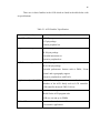
LIST OF TABLES
TABLE NO.
TITLE
PAGE
2.1
AVR Families’ Specification
3.1
JTAG Protocol Example as in ATmega 324p Datasheet 23
5.1
Connection Between JTAG board and Target Board
46
5.2
IDCODE of ATmega Microcontroller
46
5.3
Table of JTAG ID Values for ATmega 644p
47
5.4
Table of JTAG ID Values for ATmega 16 L
48
16
xi
LIST OF FIGURES
FIGURE NO.
TITLE
PAGE
1.1
JTAG Usage
2
1.2
Project Flow
5
2.1
Detailed JTAG Block Diagram for Generic Hardware 7
2.2
Electrical Characteristic of JTAG
11
2.3
TAP Controller
12
2.4
Block Diagram for Atmel AVR
17
2.5
Pin Out for ATMega 324p
19
2.6
Block Diagram for ATmega 324p
20
3.1
Proposed Design for JTAG Analyzer
22
3.2
Block Diagram of a Simple TAP Controller Connection 24
3.3
Data Function General Flowchart
25
3.4
Instruction Function General Flowchart
27
4.1
Tool Chain for AVR-GCC Compiler
30
4.2
Example Makefile
32
4.3
Example AVR-GCC Compiling
33
4.4
Proteus Design
34
xii
FIGURE NO.
TITLE
PAGE
4.5
Flow for IDCODE Program
35
4.6
IDCODE for ATmega 644p
36
4.7
IDCODE for ATmega 16L
37
5.1
Proteus Design for Simulation
40
5.2
Simulation Output
40
5.3
Excerpt of Program Showing Intended Binary Output
41
5.4
Flowchart for Simulation
42
5.5
Flowchart for final JTAG program
43
5.6
Actual Board Connections
45
5.7
Actual Board Output
45
C1
Makefile
61
C2
Command Prompt Example
62
D1
Picking a Component in Proteus
64
D2
Setting Program into Microcontroller
65
D3
Final Design and Output
65
xiii
LIST OF ABBREVIATIONS
JTAG
- Joint Test Action Group
IEEE
- Institute of Electrical and Electronic Engineers
IC
- Integrated Circuit
PC
- Personal Computer
PCB
- Printed Circuit Board
CPU
- Central Processing Unit
FPGA
- Field Programmable Gate Array
CPLD
- Complex Programmable Logic Device
ROM
- Read Only Memory
EPROM
- Erasable Programmable Read Only Memory
EEPROM
- Electrically Erasable Programmable Read Only
Memory
SRAM
- Static Random Access Memory
I/O
- Input or Output
VCC
- Voltage Input
GND
- Ground
XTAL
- External Crystal
SDK
- Software Development Kit
xiv
LIST OF SYMBOLS
kB
-
Kilobits
Mhz
-
Megahertz (frequency symbol)
Mbits/s
-
Megabits per second (Bit transfer speed symbol)
V
-
Voltage
xv
LIST OF APPENDICES
APPENDIX
TITLE
PAGE
A
Program for Simulation
52
B
Program for full JTAG function (IDCODE)
54
C
User Manual for Win AVR-GCC
60
D
User Manual for Proteus
63
CHAPTER 1
INTRODUCTION
1.1
Project Background
Joint Test Action Group (JTAG), which is the common name for what will later
be standardized as the IEEE 1149.1 Standard Test Access Port and Boundary-Scan
Architecture[1] was initially devised for testing printed circuit boards using boundary
scan and is still widely used for this application. Today, JTAG is also widely used
for IC debug ports. In the embedded processor market, essentially all modern processors
support JTAG when they have enough pins. Embedded systems development relies
on debuggers talking
to
chips
with
JTAG
to
perform
operations
like single
stepping and break pointing. Digital electronics products such as cell phones or a wireless
access point all generally do not have other debug or test interfaces.
2
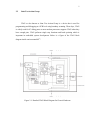
Figure 1.1: JTAG usage
JTAG will be connected to the PC and used to debug any target board containing
microprocessors as shown in the figure above. The JTAG cable in modern application
can also be used to program boards.
1.2
Problem Statement
With the advancement of technology, microprocessors have reduced in size
significantly and this in turn reduces the size of the PCB involved. This will increase the
number of possible errors that may occur on the PCB. As the size decreases, it increases
the difficulty in finding the problem. Besides that, the programs that are used will
increase and become more complicated.
This will need very long and tedious process of finding and going through the
program to locate any error or problem that might occur. Getting a program right in the
first development process is very tough and errors are expected. Therefore debugging
tools are very important. A JTAG analyzer can be used to debug the problems as well as
transfer programs to the target board. Errors can be found on PCB level by debugging the
board using single stepping and boundary-scanning.
3
Finally, JTAG analyzers are very expensive on the market. Therefore, JTAG
usage is not practical in smaller scaled applications. However, a cheaper JTAG analyzer
can minimize the cost for small scale projects while maintaining the capabilities of the
JTAG analyzer.
1.3 Objectives
The objectives of this project are:
1. To create JTAG analyzer that is able to capture and display the IDCODE of a
Atmel AVR microcontroller on the targeted board
2. To create a JTAG analyzer that is compatible with Atmel AVR processor. The
JTAG analyzer is to be compatible with all microprocessors from ATMEL AVR
family.
3. To design a simple and user friendly device that is compact and economical.
4
1.4 Scope of Project
There are always limitations or restrictions when it comes to completing a task.
For this project, the processor that is going to be used will only be an ATMEL AVR
microprocessor. The target of this is to be able to get and display the IDCODE of a
microprocessor that is of the ATMEL AVR family emphasizing on the ATMEGA.
Besides that, the programming language that will be used will be c-language.
Besides that, this project will be utilizing Win AVR-GCC as the compiler and any other
boot loader that can be compatible to the ATMEL AVR.
This project will also utilize Proteus, which is a simulation program to simulate
the inputs and outputs of microcontrollers.
5
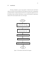
1.5
Project Flow
Literature research
about JTAG
Find technique
Choose the
and software used
best technique
for JTAG coding
analyzer
Troubleshoot if
required
Test the coding
Create the
to get the
JTAG coding
intended results
Test the coding
Optimization
onto an actual
of results
Atmel AVR board
Figure 1.2: Project Flow
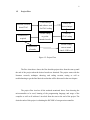
The flow chart above shows the flow that this project takes from the start up until
the end of the project when the desired results are obtained. The project starts with the
literature research, technique choosing, and coding creation, testing as well as
troubleshooting to get the final desired results that will be discussed in the next chapter.
The project flow involves all the methods mentioned above from choosing the
microcontroller to be used, learning of the programming language, and usage of the
compiler as well as all software’s involved from the start to the end of the project The
desired results of this project is obtaining the IDCODE of a target microcontroller.
CHAPTER 2
LITERATURE REVIEW
2.1
Introduction
JTAG is mainly used in boundary scanning applications on PCB boards. It also
has the ability to program target microcontrollers besides being able to perform
debugging functions. In this chapter, the various aspects are reviewed towards being able
to create a JTAG analyzer. The main target is to be able to get the IDCODE of a target
microcontroller. Besides that the programming language used, the microcontroller used
as well as the various programs that are applied to be able to get the results needed to call
this project a success is also discussed.
7
2.2
Joint Test Action Group
JTAG or also known as Joint Test Action Group is a device that is used for
programming and debugging at a PCB level using boundary scanning. These days, JTAG
is widely used for IC debug ports as most modern processors supports JTAG when they
have enough pins. JTAG performs single step functions and break pointing which is
important in embedded system development. Below is a figure of the JTAG block
diagram inside a microcontroller[1]:
Figure 2.1: Detailed JTAG Block Diagram for Generic Hardware
8
2.2.1
Debugging
JTAG was originally designed for testing printed circuit board assemblies[2]. In
current years, it has become an essential mechanism for debugging embedded systems
which may not support other debug-capable devices. Target CPU will have debug
modules which is accessible through the JTAG used as the transport mechanism.
Through these modules, software developers may debug the software of an embedded
system directly at the machine instruction level when needed.
Using JTAG to debug, processors can normally be let run freely; single stepped,
or halted according to the need of the debugger or the programmer. Most design support
‘halt mode debugging’, but some allow for debuggers to access data busses and registers
without the need for the core to be stopped. FPGA developers also use JTAG from time
to time. The same technique used to debug the software inside CPU can be used to debug
other digital design blocks inside a FPGA such as reading registers or providing visibility
for behaviours which are invisible to boundary scan operations.
9
2.2.2
Programming
Programming is another function that can be performed by a JTAG other than the
ability to perform debugging. Some devices can be programmed using the JTAG port
normally during the development period.
JTAG programmers are usually used to transfer data to internal non-volatile
memory such as CPLDs. Besides that, JTAG programmers are also used to write
software and data into flash memory. This is usually done using data bus access like CPU
in cases where the memory chip do not have JTAG interface them self[3].
2.2.3
Boundary Scan Testing
In many integrated circuits today, all pins that connect to electronic logic are
linked together in a set known as the boundary scan chain. By using JTAG to manipulate
the chip’s external interfaces such as the inputs and outputs to other chips, it is possible to
test for certain faults. The combinational logic can also be tested when the JTAG
manipulates the internal interfaces of the chip such as the on chip registers[5].
10
In both internal and external manipulation, the testing is done after it is mounted
onto a finished board and possibly while it is in a functioning system. When JTAG is
combined with the internal test known as the built in self test, the JTAG scan chain will
testing an IC for certain static faults such as shorts, opens and logic errors. Test cases are
usually provided in standardized formats and are used in production testing which is
essential in today’s products as faults can be detected on finished boards before it is
shipped out[7].
2.2.4
Electrical Characteristics
A JTAG interface is a special four or five pin interface that is added to a chip and
designed. This is so that if multiple chips are used on a board, the JTAG lines can be
daisy-chained together so that only a single JTAG port is needed to have access to all
chips on a circuit board. The five pins are TDI (Test Data In), TDO (Test Data Out), TCK
(Test Clock), TMS (Test Mode Select), and TRST (Test Reset which is optional)[8]. The
figure below shows all the connection of the above pins except the reset pin in the JTAG
chain.
11
Figure 2.2: Electrical Characteristic of JTAG
Only one data line is available, hence making the JTAG a serial protocol device.
For input data as well as the output data, both transfers data in serial. The TCK pin is the
clock input for the JTAG functions. Clocking and changes on TMS causes steps through
a standardized JTAG state machine known as the TAP controller which will be discussed
next. During each TCK pulse, one bit of data is transferred at the TDI and TDO pin.
Different instructions can be loaded such as reading of the id of a target microcontroller
or to sample inputs and outputs.
12
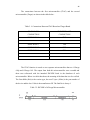
2.2.5
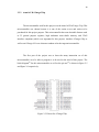
TAP Controller
To be able to understand and manipulate the JTAG analyzer, the TAP controller
must first be understood. The TAP controller is a state machine within the
microcontroller. It controls the different states that can be manipulated to be able to gain
JTAG function in that microcontroller.
The TAP controller is basically divided into two parts, the data and instruction
parts. Before entering either part, there is the reset and ideal states. From the reset state
(initial start up), the controller will enter the ideal state until further instructions direct it
to the next state. The next part is divided into two, the instruction and data functions.
Both data and instruction functions have seven states that are the same in name for both,
that are select, capture, shift, exit, pause, exit2 and update which will then either return to
ideal state or back to the select for the data or instruction register.
Figure 2.3: TAP Controller
13
The movement between states and the selection of the next state is controlled by
TMS (Test Mode Select) and TCK (Test Clock Input). On every rising edge of the TCK,
TMS will be read and will move accordingly. The state diagram of the TAP controller is
shown in figure 2.3.
The first state is the Test Logic Reset. This is the state where all the registers are
reset and the controller starts from the beginning of the state cycle. If there is any initial
condition on the controller, the 5 cycles of TMS high is needed to return the state
controller to the reset position. Alternatively, the TRST (reset) can be set low to allow the
controller to return to the reset state. The next state is the ideal state. This is the state
where the controller is in ideal mode and does not run any function unless certain special
instructions are present such as the RUNBIST which will cause a self test on the target
chip.
The first states are the scan-DR and scan-IR states. During the scan-DR, the
controller will acknowledge the value of TMS on the rising edge of TCK to see the next
route, weather to go into the capture-DR (TMS=0) or scan-IR (TMS=1) state. When in
the scan-IR state, the controller will acknowledge the value of TMS to check whether to
proceed into the capture-IR (TMS=0) or back to the reset state (TMS=1).
The following state is the capture state. In the capture-IR state, a set of
instructions is moved into the instruction register. For the capture-DR state, data is
moved in parallel into the selected data register according to the instruction set. Next is
the shift state. In the shift-IR, the shift register is connected between TDI and TDO to
shift data out while in the shift-DR state, the test data register is connected between TDI
and TDO to shift out data regarding the test.
14
The exit-DR and exit-IR is a temporary state in which the value of TMS will
choose the next path whether it be pause (TMS=0) or update (TMS=1). The pause–DR
and pause-IR states will allow for movement of the serial data between TDI and TDO to
be temporarily be halted. Then comes the exit2-DR and exit2-IR which is another
temporary state where the value of TMS will select the next path whether it be update
(TMS=1) or back to shift (TMS=0).
Finally, the final state is the update-IR and update-DR. In this state, the register
will latch the next instruction or data that is to be captured in the following capture state.
In this state, when TMS is held high for a rising edge of TCK, the controller will proceed
to the select states. If TMS is set to low, the state will return to the ideal state.
For both Instruction and Data functions, the general flow is as described above,
that it moves from scan to capture, shift, exit2, pause, exit2 update and back to scan or
idle. This is the general state movement. However, this movement can be manipulated by
manipulating the values of TMS as will be done in this project.
As an example, the values of TMS can be manipulated to obtain the IDCODE of
the microcontroller that is being tested. To get the IDCODE, the TAP must go through
the Instruction function first. This is to send the input data to the instruction register. Next
is to go through the Data register to obtain the IDCODE.
15
Referring to the TAP controller diagram in figure 2.3, the values 0, 1, 1, 0, and 0
is inserted to TMS to go through the instruction register up to the shift state. Then, to
shift the data in from TDI, TMS is held low for four TCK cycles to remain at the shift
state. Then, the values 1, 1, and 1 is inserted to TMS to exit and update and go to the next
function that is the Data function. At the data function, the same process as above is
repeated. This time, TMS is held low for 32 cycles at the shift state because the output is
a 32-bit data.
2.3
Atmel AVR
These microcontrollers are a modified Harvard architecture 8-bit RISC single chip
microcontroller. These chips were developed by Atmel in 1996 and were the first
microcontroller to use on-chip flash memory. This is as opposed to one time
programmable memories such as ROM, EPROM or EEPROM that were being used by
other microcontrollers at that time. These microcontrollers have separated physical
memory systems. These memories appear in different address spaces to store data and
programs but have special instructions to read data from program memories.
16
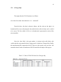
There are six basic families in the AVR which are listed in the table below with
its specifications:
Table 2.1: AVR Families’ Specification
AVR family
tinyAVR – ATtiny series
Specifications
-
0.5-8kB program memory
-
6-32 pin package
-
Limited peripheral set
megaAVR – Atmega series -
4-256kB program memory
-
28-100 pin package
-
Extended instruction set
-
Extensive peripheral ser
XMEGA – Atsmega series -
16-384kB program memory
-
44-64-100 pin package
-
Extended performance features such as DMA, ‘Event
System’ and cryptography support
Application – Specific AVR-
Extensive peripheral set with DACs
MegaAVRs with special features not found on other
members of the AVR family such as LCD controller,
USB controller advanced PWN CAN etc.
FPSLIC – AVR with FPGA -
32-bit AVRs
FPGA 5K to 40K gates
-
SRAM for the AVR program code
-
AVR core can run up to 50MHz
-
Consists of several micro-architectures
-
Cost sensitive application
17
2.3.1
Device Architecture
For Atmel AVRs, Flash, SRAM, and EEPROM are all integrated onto a single
chip. This removes the need for external memory in most applications. Some devices
allow additional data memory or memory-mapped devices by having parallel external bus
option. Below is a block diagram of the AVR architecture[6]:
Figure 2.4: Block Diagram for Atmel AVR
18
Program instructions are saved in non-volatile flash memory. The size of the
program memory is usually indicated by the name of the device itself. For example,
ATmega64x has 64kB of flash memory to be utilized. Internal data address space consists
of the I/O registers, SRAM and register file. In most AVRs, the working registers are
mapped in the first 32 memory addresses, followed by the 64 I/O registers, which is
followed by the SRAM.
Almost all AVR also have EEPROM for semi-permanent data storage which can
be maintained even without electrical power. In most AVRs, this EEPROM has to be
accessed like accessing an external peripheral by using special pointer register and
read/write instructions which makes access to EEPROM much slower.
Atmel AVRs are made with a two stage, single pipeline design. This means that
when the current instruction is being executed, the next instruction is already being
fetched. Most instructions take only one or two clock instruction which makes AVRs
relatively fast. These processors were developed with the efficient execution of compiled
C code in mind and therefore have many built-in pointers for this task[6].
19
2.3.2
Atmel AVR ATmega 324p
The microcontroller used for this project was the Atmel AVR ATmega 324p. This
microcontroller was chosen because it is one of the easiest to use and easiest to be
purchased for this project purpose. This microcontroller has some desirable features such
as 32 general purpose registers, high endurance non-volatile memory, and JTAG
interface compliant (which was important for this project). Another ATmega 624p as
well as an ATmega 16L were chosen at random to be the target microcontroller.
The first part of the project was to learn the many instruction set of this
microcontroller as to be able to program it to be used to the need of this project. The
block diagram[9] for this microcontroller as well as the pin out[9] is shown in figure 2.5
and figure 2.6 respectively:
Figure 2.5: Pin out for ATmega 324p
20
Figure 2.6: Block Diagram for ATmega 324p
For this project, the most important pins are those at port b, and port c. Port b will
be the port that is used to send the JTAG instructions to the target board. Port c is the port
that has the function specific pins for the JTAG functions that are the TCK, TMS, TDI
and TDO pins. The VCC, GND, and XTAL are also used for the external cock as well as
for powering up the microcontroller.
The Atmel AVR microcontroller supports C language as well as assembly
language. However, for this project purpose, the C language is preferred. This is because
of its simplicity and previous experience using this language to be able to create the
required program to get the IDCODE through the JTAG interface.
CHAPTER 3
PROPOSED DESIGN OF A JTAG ANALYZER
3.1
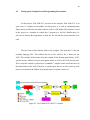
Introduction
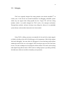
This chapter discusses the development of a JTAG analyzer for this project.
All the problems faced and the solutions to overcome them are also discussed in this
chapter. Figure 4.1 shows a proposed design of a JTAG analyzer. The outputs from
PortB from the JTAG are connected to the JTAG pins on the target microcontroller
22
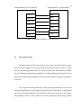
Microcontroller 1(JTAG Analyzer)
Microcontroller 2 (Target Board)
PORT B 1
TMS
PORT B 2
TRST
PORT B 5
TDI
PORT B 7
TCK
PROT C 0
TDO
VCC
VCC
GND
GND
Figure 3.1: Proposed Design for JTAG Analyzer
3.2
The JTAG Protocol
Literature review on JTAG was done on all previous work. This includes all past
projects, online solutions as well as specification and technical papers. However, at this
step, the first hurdle presented itself. For JTAG, the only clear documentation available
was the technical and specification datasheet. All online solutions or past projects were
giving out the final solution and did not provide inside towards creating a JTAG analyzer
on its own.
This, coupled with the fact that most JTAG protocol and instructions set found in
Atmel AVR datasheets are kept private, meant that the only valid source of information
was from the technical datasheet. The table below shows an excerpt from an ATmega
644p datasheet with the JTAG protocols. All other journals and books only provided
23
information on the JTAG analyzer or on its architecture. This only led to the
understanding of the functions of JTAG and its uses. However, this did not help much in
the development of the software which had to be done from scratch.
Table 3.1: JTAG Protocol Example as in ATmega 324p Datasheet
JTAG Instructions
Function Done
PRIVATE 0x8
Private JTAG instruction
PRIVATE 0x9
Private JTAG instruction
PRIVATE 0xA
Private JTAG instruction
PRIVATE 0xB
Private JTAG instruction
Therefore, it became important to understand the technical and specification
documents. This took a large amount of time as the papers had to be understood and a lot
of trial and error had to be done in the process of obtaining a clear understanding of the
internal functions of JTAG namely the TAP controller.
The specifications and technical documents mention on the internal functions of
the JTAG as well as all the registers that are at hand. However, these papers do not
mention the relevant codes and syntaxes to be used in writing the source code that is to
do a JTAG function. Therefore, trial and error method had to be implemented to
understand the papers and decipher them to make a working source code.
24
Actual output from an industrial based JTAG was also needed as to be able to
cross reference the output from an actual JTAG with the output obtained in this project.
The JTAGICE MKII was used for this purpose. The JTAGICE requires external power
and therefore the SDK board being tested needed to be powered using a USB tiny. This
JTAGICE was used to program the board as well as to obtain the IDCODE to gain some
data to cross reference the actual output of the JTAG analyzer that is designed
3.3
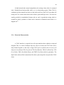
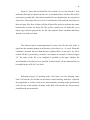
JTAG TAP Controller Flow
The figure below shows a block diagram of a simple TAP Controller. The general
movement between the states in a TAP function to run the various functions of a JTAG.
The flowcharts show the movement is states through the data registers (figure 3.3) and
instruction registers (figure 3.4).
Atmel AVR Microcontroller
TMS
TCK
TDI
TDO
TRST
TAP Controller
Registers to be
manipulated
Boun
dary
Scan
Chain
JTAG
interface
Figure 3.2: Block Diagram of a Simple TAP Controller connection
25
START
From TMS
selector of
IR Flow
(NO)
NO
Enter Ideal State
NO
TMS
= 1?
From TMS
selector of
IR Flow
(YES)
YES
YES
Enter Select DR-Scan
TMS
= 1?
YES
NO
Enter Capture DR
YES
TMS
= 1?
NO
Enter Shift DR
TMS
= 1?
YES
Enter Exit1
NO
Go to IR flow
26
TMS
= 1?
YES
NO
Enter Pause DR
NO
TMS
= 1?
YES
Enter Exit2
NO
TMS
= 1?
YES
Enter Update DR
TMS
= 1?
Figure 3.3: Data Function General Flowchart
27
From Data
Flow
Enter Select IR-Scan
TMS
= 1?
YES
NO
Enter Capture IR
YES
TMS
= 1?
NO
Enter Shift IR
TMS
= 1?
NO
YES
Enter Exit1
TMS
= 1?
NO
Enter Pause IR
YES
Back to Reset
28
NO
TMS
= 1?
YES
Enter Exit2
NO
TMS
= 1?
YES
Enter Update IR
Back to Data
Flow (Ideal)
NO
TMS
= 1?
YES
Back to Data
Flow (Select
DR-Scan)
Figure 3.4: Instruction Function General Flowchart
CHAPTER 4
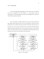
IMPLEMENTATION OF THE PROPOSED JTAG ANALYZER
4.1
Introduction
This chapter discusses the implementation of the theories of designing a JTAG
analyzer. The compilation and programming environment as well as the electrical design
and software development are discussed in detail. This chapter also discusses the output
that will be used to cross reference with the output from the JTAG analyzer that is to be
created.
30
4.2
Setting up the Compilation and Programming Environment
For this project, Win AVR-GCC was used as the compiler. Win AVR-GCC is an
open source C compiler and assembler. For this project, it is used in command prompt
format and is not linked to any other software such as AVR Studio. This software is used
in this project as a compiler to compile the C program to a .hex file. Besides that, it is
also used to instruct the programmer to burn the .hex file into the microcontroller to be
used.
The tool chain of this software starts at the compiler. This turns the C code into
assembly language files. This software has an avr-libc which is the C library for the
AVR. This includes all the header files that contain all the floating point library, AVRspecific macros, addresses of port and register names as well as the AVR start-up code.
This is why this compiler is preferred to a standard C compiler which would not have all
this information for the AVR. Therefore, it would require the user to write a start up code
and so on to initialize the address of ports and names of registers and so on.
Figure 4.1: Tool Chain for AVR-GCC Compiler
31
Figure 4.1 shows the tool chain flow of a creation of a .hex file from the C code
and header files that are inputs from the user. As mentioned above, all these files will be
converted to assembly files. Once these assembly files are obtained, they are converted to
object files. These object files are a level of code that the AVR could run itself, however
there are many files. Here, a linker will take all these files and cross-reference the names
between files to create one object file. This will be created as an .elf format file, so an
object copy is done to generate the .hex file. The compiler, linker, assembler and library
form the core of the tool chain.
This software runs in command prompt. To create a .hex file, the word ‘make’ is
typed into the command prompt at the directory where there is a c is saved. When this
command is inserted, the tool chain that was explained above is run and a .hex file is
created. All this is governed by a makefile. An example of a makefile is shown in figure
4.2. The name of the file to be compiled is specified at the target. Besides, the
microcontroller used also has to be specified. In this makefile, all the functions that can
be handled by the AVR-GCC are listed.
Referring to figure 4.2, inserting ‘make’ will create a .hex file. Inserting ‘make
clean’ will clear the .hex file that was previously created. Inserting ‘make fuse’ will allow
the programmer to set fuses values to the microcontroller according to the specifications
set by the user in the makefile. Inserting ‘make flash’ will burn the .hex file previously
created into the microcontroller.
32
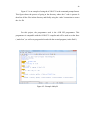
Figure 4.3 is an example of using the AVR-GCC in the command prompt format.
This figure shows the process of going to the directory where the C code is present. It
then lists all the files in that directory and finally using the ‘make’ instruction to creates
the .hex file
For this project, the programmer used is the AVR ISP programmer. This
programmer is compatible with the AVR-GCC compiler and will be used to set the fuses
(‘make fuse’) as well as to program the board with the created program (‘make flash’).
Figure 4.2: Example Makefile
33
Figure 4.3: Example AVR-GCC Compiling
4.3
Electrical Design of JTAG Analyzer
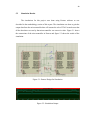
For simulation purposes, Proteus was the software used in this project. This
Proteus software was made to be used for microprocessor simulation, schematic capture,
and printed circuit board design. In this project, this software is used to draw the
microcontroller connection and do the simulations. This is to confirm that the generated
output match the intended output before going to the actual board implementation.
Proteus consists of drawing circuits from set devices in the library and connection
as intended. After this is done, various ways of simulation can be done after the .hex file
is inserted into the microcontroller in the settings. This software can then simulate the
34
outputs at all pins involved with the simulation that is being done. This software also
supports creation of timing diagrams to show the outputs of pins according to the user’s
needs which is one of the features that will be used in this project.
Figure 4.4 shows an example of a connection between two microcontroller and
the probes that are in place to generate the timing diagram (more of which will be
discussed in the following chapter). However, Proteus can only generate the output of the
first microcontroller and is not able to get an output from the second microcontroller
because this software does not simulate the JTAG functions of the microcontroller.
Figure 4.4: Proteus Design
35
4.4
Software Development for Manipulating TAP Controller
A flowchart is designed by manipulation the values of the TMS to go through the
TAP controller to obtain the IDCODE. The figure below shows the flow of the program
to obtain the IDCODE from a target microcontroller.
IDEAL STATE
SELECT DR-SCAN
SELECT IR-SCAN
CAPTURE IR
SHIFT IR
EXIT1
UPDATE IR
SELECT DR-SCAN
CAPTURE DR
SHIFT DR
EXIT1
36
UPDATE DR
Figure 4.5: Flow for IDCODE Program
The next step was to use the actual industry based JTAG which is the JTAG ICE
MKII. This device is used to check the output of the IDCODE to later e cross referenced
with the output of the JTAG created for this project. Below are two figures that show the
output of the IDCODE. Figure 4.6 shows the IDCODE for an ATmega644p and figure
4.7 shows the IDCODE for an ATmega16L. Both these IDCODE are found to be correct
according to the datasheet and therefore will be used as a base to compare with the actual
output of the JTAG for this project (discussed in the next chapter).
Figure 4.6: IDCODE of ATmega 644p
37
Figure 4.7: IDCODE of ATmega 16L
The program was written in C language because it is simpler compared to
assembly language. The first step was to create a source code to simulate the outputs
required. This source code that was created (Appendix A) was tested using Proteus
(Results discussed in next chapter) and the output of the simulation was checked with the
required inputs.
The first hurdle that was faced in this process was the output generated. The
program was tweaked several times by changing the delay and placements of several
codes in the source code to finally obtain the intended output. Once the accurate output
has been obtained, the remaining part of the program could be created. This was the part
that included the process in the TAP controller and the sending of instruction and
receiving of data from the registers. The data to be sent and received were placed all in
38
the rising edge of TCK portion in the program. This program was then tested on the
actual board.
This is where the next problem occurred. The outputs were not as expected. The
results obtained were nowhere close to the expected results. Further research on the
technical papers proposed a solution. The output portion of the program, which is the part
where TDO sends the output back to the JTAG (first microcontroller), was wrong. All
outputs from target were to be in the falling edge of the TCK. After rectifying this
problem, the output was still found to be incorrect. At this point, various trial and error
methods were implemented. First, the portion of the program that received the data from
TDO was shifted up and down the timing cycle. This means, that the program was
modified to receive that data earlier or later that the original program. However, this did
not solve the problem.
Next, the program was shifted by several bits to see if any similarities were found
in the output compared to the intended data in the datasheet. When this failed, the output
was analyzed with a different method. The position of the output data was analyzed.
Finally, it was found that the arrangement of the display in the program was reverse.
After rectifying this problem, the output of the JTAG was found to be correct. To make
sure that this was correct data, the JTAG function was tested on a second microcontroller
and the output was also found to match the intended output in the datasheet (discussed in
the next chapter).
CHAPTER 5
RESULTS AND DISCUSSION
5.1
Introduction
This chapter will be discussing all the results that were acquired and analyzed
throughout this project. This chapter will cover all the results from the simulations done
as well as the actual data that was tested onto the WISE SDK board. All this data were
analyzed and compared to the intended data to be verified as will be discussed in this
chapter.
40
5.2
Simulation Results
The simulations for this project were done using Proteus software as was
described in the methodology section of this report. The simulation was done to gain the
output data from the microcontroller that will assume the role of JTAG to make sure that
all the data that were sent by that microcontroller was correct in value. Figure 5.1 shows
the connections of the microcontroller in Proteus and figure 5.2 shows the results of the
simulation:
Figure 5.1: Proteus Design for Simulation
Figure 5.2: Simulation Output
41
Figure 5.1 shows the microcontroller that is to function as the JTAG (U1) with the
pins from port b being connected to the JTAG input pins of the second microcontroller.
However, Proteus is not able to simulate the JTAG functions and therefore this
simulation is done just to verify that the outputs of the microcontroller to simulate the
JTAG are as expected. The source code that is to be tested is loaded into the first
microcontroller and then the simulation is done. The source code is located in the
appendix (Appendix A).
In the simulation, the four pins act as an output (TMS, TCK, TDI and TRST)
from the microcontroller are tested by attaching a probe to the wire lines of the pins that
are to be tested. Then a digital analysis chart is opened and the values of the lines that are
attached to the probe will be displayed when the simulation is done. This information is
then cross checked with the intended output to make sure that the data is correct.
Below is the figure that shows the portion of the program that is used (attached in
the appendix) for this simulation. This figure shows the intended output of the
microcontroller as described in the program and it is found that the output in figure 5.2
corresponds to the intended output.
Figure 5.3: Excerpt of Program Showing Intended Binary Output
42
Below is the flowchart for the simulation of the output for the microcontroller that
is to function as a JTAG:
START
INITIALIZE VALUES
(TMS, TDI, TDO, TCK, TRST)
SEND VALUES TO PORT
DISPLAY VALUES
END
Figure 5.4: Flowchart for Simulation
43
5.3
Actual Board
After the verification is correct, the program is burned onto the actual board
which is the WISE AVR Mice SDK board. The program was done with C programming
on notepad and then compiled using Win AVR-GCC to compile the program into a hex
file and then to burn it onto the board. Below is a figure of the flowchart to send the data
from the JTAG microcontroller and to receive the output:
START
INITIALIZE VALUES
(TMS, TDI, TDO, TCK, TRST)
SEND VALUES TO SECOND
MICROCONTROLLER
GET RETURN TDO VALUE
SEND TDO VALUE TO PORT
DISPLAY TDO VALUE ON LED
END
Figure 5.5: Flowchart for the Final JTAG Program
44
The microcontroller that has been burned with the program is the main
microcontroller that will function as the JTAG. This microcontroller is then connected to
the second microcontroller that is to be tested. The output pins are connected to the JTAG
pins of the microcontroller that is to be tested on the second board and the program will
be executed.
The main board, that is the JTAG board, will be powered by the ISP programmer
and the common VCC and GND that is connected between the two boards will power the
second board. Below are two pictures (figure 5.6 and figure 5.7) that show the connection
and the output of the actual board.
When the program runs, the JTAG values as was verified in the simulations will
be sent to the JTAG pins on the second board. This will then enter the TAP controller of
the second microcontroller. The JTAG instructions as in the TAP controller will run as
previously described (Chapter 2). When the JTAG functions are completed, the output
will be sent to the L.E.D port. The output is a 32-bit data. Therefore the data will be
shown on the 8 L.E.D on the SDK board in four blinks that last 1 second each. This
duration can however be adjusted in the program that is burned into the microcontroller.
The source code for this portion is located in the appendix (Appendix B).
These values that are shown at the L.E.D are cross referenced with the intended
values that are in the datasheet that shows all the IDCODES for the microcontroller in
question.
45
Figure 5.6: Actual Board Connections
Figure 5.7: Actual Board Outputs
46
The connections between the first microcontroller (JTAG) and the second
microcontroller (Target) are shown in the table below:
Table 5.1: Connections Between JTAG Board and Target Board
JTAG BOARD
TARGET BOARD
CONNECTION
CONNECTION
PORT B PIN 1
TMS
PORT B PIN 2
RESET
PORT B PIN 5
TDI
PORT B PIN 7
TCK
PORT C PIN 0
TDO
VCC
VCC
GND
GND
The JTAG function is tested on two separate microcontrollers that are ATmega
644p and ATmega 16L. The output from both this microcontroller were recorded and
then cross referenced with the intended IDCODE listed in the datasheet of each
microcontroller. Below is a table that shows the meaning of the data that is to be verified.
The first nibble (4bit) is the version type, the next 2 bytes (16bits) is the part number of
the device and the last 11 bits is the manufacturer ID. The final bit is always 1.
Table 5.2: IDCODE of ATmega Microcontroller
47
5.3.1
ATmega 644p
The output after the JTAG functions is as follows:
0110 1001 0110 0000 1010 0000 0011 1111 = 6960A03F
From the above, the data is shown in binary, and the value on the right is in
hexadecimal. By cross referencing the data with the below table, the data can be verified
to be correct. The first, which is 0110 or 6 in hexadecimal, represents the version of the
microcontroller.
Next, the value 960A is the part number. As shown in the table below, this
verifies that the microcontroller that is being tested is indeed an ATmega 644p. Finally,
the manufacturing ID is supposed to be 01F. However, due to parity error, an extra 1 has
entered the data to make to manufacturer ID 03F instead for the output of this project.
Table 5.3: Table of JTAG ID Values for ATmega 644p
48
5.3.2
ATmega 16L
The output after the JTAG functions is as follows:
0000 1001 0100 0000 0011 0000 0011 1111 = 0940303F
From the above, the data is shown in binary, and the value on the right is in
hexadecimal. By cross referencing the data with the below table, the data can be verified
to be correct. The first, which is 0000 or 0 in hexadecimal, represents the version of the
microcontroller. From the table below, the version for this microcontroller is revision A.
Table 5.4: Table of JTAG ID Values for ATmega 16L
Next, the value 9403 is the part number. As shown in the table above, this verifies
that the microcontroller that is being tested is indeed an ATmega 16 L. Finally, the
manufacturing ID for this microcontroller is 03F.
CHAPTER 6
CONCLUSION AND RECOMENDATION
6.1
Conclusion
As a conclusion, the objectives of this project were achieved. The correct
IDCODE was able to be extracted from the Atmel AVR microcontroller. Two different
Atmel AVR microcontrollers were used ATmega 644p and ATmega 16L so as to make
sure that two different set of results could be obtained. Using simulations and actual
board applications, it was found that the programming and actual applications produced
the intended IDCODE from an Atmel AVR microcontroller.
The project followed the flow of creating a C program before running simulations
confirm the outputs of the program. Then the verified program was burned onto an Atmel
AVR microcontroller and the JTAG function was tested on other Atmel AVR
microcontrollers. At the end of this project, the all the objectives were completed and the
50
correct IDCODE was extracted and displayed at the outputs. The program created was
user friendly and can be easily understood and edited to do more functions in the future.
6.1
Recommendations
At the end of this project, a few improvements can be done for future students or
future studies on JTAG as listed below:
1.
This project can be used as a stepping stone for future studies about JTAG.
2.
The various private functions in the list of JTAG protocols can be deciphered by
using logic analyzer to analyze the communication between JTAG ICE and Atmel AVR
microcontroller.
3.
By using this project as the first step, and together with the analyzed information
from the logic analyzer, advancements can be made to make a more user friendly and
complete JTAG analyzer.
4.
Further verifications for the IDCODE can be done by using microcontrollers form
different manufacturers such as ALTERA, ARM or any other device that supports JTAG
functions.
51
REFERENCE
1. Institute of Electrical and Electronics Engineers. Standard Test Access Port and
Boundary-Scan Architecture. United States of America, 1993.
2. Be Van Ngo, P.Law and A.Sparks. Use of JTAG boundary-scan for testing electronic
circuit boards and systems. AUTOTESTCON 2008
3. Ping Zhang, Yanmin Song, Jianmin Zhang, Zuocheng Xing. Design of Testing
Structure in Microprocessor Based on JTAG. ISCID 2009. Vol. 1, 223 - 226
4. K.Rosenfeld, R.Karri. Attacks and Defenses for JTAG. Design & Test of Computers.
IEEE. 2009
5. Shen Xu Baang, Liang Song Hai. Design and Implementation of a JTAG boundaryscan interface controller. Proceedings of the second Asian Test Symposium. 1993
215 – 218.
6. Korbel, S. Interesting Applications of Atmel AVR Microcontrollers. Euromicro
Symposium on Digital System Design. Czech Tech University. IEEE. 2004. 499-506
7. Dettmer, R. JTAG-Setting the Standard for Boundary-Scan Testing, IEE Review.
IEEE. 1989. 49-52
8. Maunder, C. Joint Test Action Group, Computer-Aided Engineering Journal. British
Telecom, United Kingdom. IEEE. 1986. 121-122
9. Atmel Corporation. 8-bit Microcontroller Datasheet for ATmega 164p,324p,644p.
United States of America.2010
10. Mitra, S. Design for Testability and Testing of IEEE 1149.1 TAP Controller. VLSI
Test Symposium. Intel Corp. Sacramento CA. IEEE. 2002. 247-252
11. Pierce, L. Multi-Level Secure JTAG Architecture, On-Line Testing Symposium.
Department of Electric and Computer Engineering. Carbondale, IL. IEEE. 2011. 208209
52
APPENDIX A
Program for Simulation
// Program to get the idcode of the target board
#define F_CPU 20000000UL
#define setb(port, pin) port|=(1<<pin)
#define offb(port, pin) port&=~(1<<pin)
#define togb(port, pin) port^=(1<<pin)
#include <stdio.h>
#include <avr/io.h>
#include <util/delay.h>
int main ()
{
int
x[56]
=
{1,1,1,1,1,0,1,1,0,0,0,0,0,0,1,1,1,0,0,0,0,0,0,0,0,0,0,0,0,0,0,0,0,0,0,0,0,0,0,0,0,0,0,0,0,0,0,
0,0,0,0,1,1,1,1,1};
int i,TMS,TDI,TRST;
DDRB = 0xFF;
PORTB = 0x00;
DDRC=0x00;
_delay_ms(0.1);
for(i=0;i<56;i++)
{ setb(PORTB,7);
53
TMS=x[i];
if (i==0)
{ TRST=1;
TDI=0; }
else if(i==13)
{ TRST=0;
TDI=1; }
else
{ TRST=0;
TDI=0; }
if (TMS==0)
{ offb(PORTB,1); }
else
{ setb(PORTB,1); }
if (TDI==0)
{ offb(PORTB,5); }
else
{ setb(PORTB,5); }
if (TRST==0)
{ setb(PORTB,2); }
else
{ offb(PORTB,2); }
_delay_ms(0.5);
togb(PORTB,7);
_delay_ms(0.5);
}
return 0;}
54
APPENDIX B
Program for Full JTAG Function (IDCODE)
// Program to get the idcode of the target board
#define F_CPU 20000000UL
#define setb(port, pin) port|=(1<<pin)
#define offb(port, pin) port&=~(1<<pin)
#define togb(port, pin) port^=(1<<pin)
#include <stdio.h>
#include <avr/io.h>
#include <util/delay.h>
int main ()
{
int
x[56]
=
{1,1,1,1,1,0,1,1,0,0,0,0,0,0,1,1,1,0,0,0,0,0,0,0,0,0,0,0,0,0,0,0,0,0,0,0,0,0,0,0,0,0,0,0,0,0,0,
0,0,0,0,1,1,1,1,1};
int i,TMS,TDI,TRST;
DDRB = 0xFF;
PORTB = 0x00;
DDRC=0x00;
_delay_ms(0.1);
for(i=0;i<56;i++)
{ setb(PORTB,7);
55
TMS=x[i];
if (i==0)
{ TRST=1;
TDI=0; }
else if(i==13)
{ TRST=0;
TDI=1; }
else
{ TRST=0;
TDI=0; }
if (TMS==0)
{ offb(PORTB,1); }
else
{ setb(PORTB,1); }
if (TDI==0)
{ offb(PORTB,5); }
else
{ setb(PORTB,5); }
if (TRST==0)
{ setb(PORTB,2); }
else
{ offb(PORTB,2); }
_delay_ms(0.5);
togb(PORTB,7);
if(i==19)
{ a=(PINC & 0x01); }
if(i==20)
56
{a=(a<<1);
a=a+(PINC & 0x01); }
if(i==21)
{ a=(a<<1);
a=a+(PINC & 0x01); }
if(i==22)
{ a=(a<<1);
a=a+(PINC & 0x01); }
if(i==23)
{ a=(a<<1);
a=a+(PINC & 0x01); }
if(i==24)
{ a=(a<<1);
a=a+(PINC & 0x01); }
if(i==25)
{ a=(a<<1);
a=a+(PINC & 0x01); }
if(i==26)
{ a=(a<<1);
a=a+(PINC & 0x01); }
if(i==27)
{ b=(PINC & 0x01); }
if(i==28)
{ b=(b<<1);
b=b+(PINC & 0x01); }
if(i==29)
{ b=(b<<1);
57
b=b+(PINC & 0x01); }
if(i==30)
{ b=(b<<1);
b=b+(PINC & 0x01); }
if(i==31)
{ b=(b<<1);
b=b+(PINC & 0x01); }
if(i==32)
{ b=(b<<1);
b=b+(PINC & 0x01); }
if(i==33)
{ b=(b<<1);
b=b+(PINC & 0x01); }
if(i==34)
{ b=(b<<1);
b=b+(PINC & 0x01); }
if(i==35)
{ c=(PINC & 0x01); }
if(i==36)
{ c=(c<<1);
c=c+(PINC & 0x01); }
if(i==37)
{ c=(c<<1);
c=c+(PINC & 0x01); }
if(i==38)
{ c=(c<<1);
c=c+(PINC & 0x01); }
58
if(i==39)
{ c=(c<<1);
c=c+(PINC & 0x01); }
if(i==40)
{ c=(c<<1);
c=c+(PINC & 0x01); }
if(i==41)
{c=(c<<1);
c=c+(PINC & 0x01); }
if(i==42)
{ c=(c<<1);
c=c+(PINC & 0x01); }
if(i==43)
{ d=(PINC & 0x01); }
if(i==44)
{ d=(d<<1);
d=d+(PINC & 0x01); }
if(i==45)
{ d=(d<<1);
d=d+(PINC & 0x01); }
if(i==46)
{ d=(d<<1);
d=d+(PINC & 0x01); }
if(i==47)
{ d=(d<<1);
d=d+(PINC & 0x01); }
if(i==48)
59
{ d=(d<<1);
d=d+(PINC & 0x01); }
if(i==49)
{ d=(d<<1);
d=d+(PINC & 0x01); }
if(i==50)
{ d=(d<<1);
d=d+(PINC & 0x01); }
_delay_ms(0.1); }
PORTB=d;
_delay_ms(1000);
PORTB=c;
_delay_ms(1000);
PORTB=b;
_delay_ms(1000);
PORTB=a;
_delay_ms(1000);
PORTB=0x04;
return 0;
}
60
APPENDIX C
User Manual for WIN AVR-GCC
WIN WVR-GCC is an open source software development tools for Atmel AVR
series of microcontroller hosted on Windows platform. It includes CNU compiler for C
and C++ programming. WIN AVR includes all tools for developing on AVR which
includes compiler, programmer, debugger and more. This software can be found at
http://winavr.sourceforge.net/.
This software is free to download from the above mentioned website. The
installation process is simple. First, download the executable file. To be installed, just run
the .exe file and follow the installation process.
This software is easy to use. It is a command prompt based program. To be used,
the command prompt is open in the directory where the .c program to be compiled is
saved. Using the command prompt, several instructions can be used to compile the
program, burn it into the microcontroller and many more. All this functions are governed
by a makefile. Below are two figures that shows example of a make file and the usage of
the command prompt for compiling.
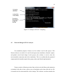
61
Appendix C1: Makefile
The above figure shows an example of a makefile. To use WIN AVR, avr-gcc is
written in the CC part of the makefile (first line in the above figure). The name of the
program to be compiled is inserted in the target portion of the makefile (line four). The
commands used are ‘make clean’, ‘make flash’ and ‘make fuse’. Clean is used to delete
the .hex file that exists in the particular directory. Flash is used to burn the program into
the microcontroller. Fuse is used to set the fuses into the microcontroller. The main
function is ‘make’. When ‘make’ is typed into the command prompt, the .hex file is
created.
62
Appendix C2: Command Prompt Example
The above figure is of an example of the command prompt using WIN AVRGCC. To use the compiler and programmer functions, the command prompt must be in
the directory where the C file is saved. Then by using the commands as mentioned above,
the program can be compiled and burned into the microcontroller.
63
APPENDIX D
User manual for Proteus
Proteus is software that is required to be bought. This trial version of this software
may be downloaded on www.download.cnet.com. This will be a version that has
limitations on the time that it can be used as well as the functions that can be done by the
software. Once the trial or full version has been obtained, the software can then be
installed by just running the .exe file and follow the installation process till the end.
This software is easy to use. Once installed, there will be two programs, ARES
and ISIS. For the microcontroller design, ISIS is used. The first step is to open the
program. To begin the design, simply click on the pick component from library button
and choose the required component and place it in the workplace (figure Appendix D1).
Once the design is done, double click on the microcontroller to set the program file into
the microcontroller (figure Appendix D2). Logic analyzing can be done by attaching
probes to the wires, opening the logic analyzer and running the program. The data will be
displayed as a timing diagram. (Appendix D3).
64
Set to component
mode
Click to open the
component library
Appendix D1: Picking a Component in Proteus
Pick the desired
component
65
Browse and select the
.hex file to insert the
program
Double-click to open
the component
Appendix D2: Setting Program into Microcontroller
settings
Probes
Logic
analyzer
with the
output
Appendix D3: Final Design and Output