1
X702/X703
Hardware User’s Manual
Warranty
All products manufactured by ICP DAS are warranted against
defective materials for a period of one year from the date of delivery to
the original purchaser.
Warning
ICP DAS assume no liability for damages consequent to the use of
this product. ICP DAS reserves the right to change this manual at any
time without notice. The information furnished by ICP DAS is believed to
be accurate and reliable. However, no responsibility is assumed by ICP
DAS for its use, nor for any infringements of patents or other rights of
third parties resulting from its use.
Copyright
Copyright 2003 by ICP DAS. All rights are reserved.
Trademark
The names used for identification only maybe registered trademarks
of their respective companies.
X702/X703 User’s Manual, Nov/2004, Rev. 1.0
------
1/59
Table of Contents
1.
GENERAL INTRODUCTION.......................................................................4
1.1.
5V Encoder Signal Wiring .....................................................................8
1.1.1.
X702: Differential Encoder & Int_5V ...........................................9
1.1.2.
X702: Single-ended Encoder + Int_5V........................................10
1.1.3.
X702: Differential Encoder + Ext_5V.........................................11
1.1.4.
X702: Single-ended Encoder + Ext_5V ......................................12
1.1.5.
X703: Differential Encoder + Int_5V ..........................................13
1.1.6.
X703: Single-ended Encoder + Int_5V........................................14
1.1.7.
X703: Differential Encoder + Ext_5V.........................................15
1.1.8.
X703: Single-ended Encoder + Ext_5V ......................................16
1.2.
12V Encoder Signal .............................................................................17
1.2.1.
X702: Differential Encoder + Ext_12V.......................................18
1.3.
1.4.
1.5.
1.6.
2.
1.2.2.
X702: Single-ended Encoder + Ext_12V ....................................19
1.2.3.
X703: Differential Encoder + Ext_12V.......................................20
1.2.4.
X703: Single-ended Encoder + Ext_12V ....................................21
24V Encoder Signal .............................................................................22
1.3.1.
X702: Differential Encoder + Ext_24V.......................................23
1.3.2.
X702: Single-ended Encoder + Ext_24V ....................................24
1.3.3.
X703: Differential Encoder + Ext_24V.......................................25
1.3.4.
X703: Single-ended Encoder + Ext_24V ....................................26
Mixed Configuration............................................................................27
Encoder Counting Mode ......................................................................29
XOR Control........................................................................................30
I/O CONTROL REGISTER.............................................................................33
2.1.
I/O Control Registers of X702.............................................................33
2.1.1.
Set Encoder Counting Mode........................................................34
2.1.2.
Read A/B/Z & Encoder Counting Mode......................................35
2.1.3.
Encoder1 24-bit Value..................................................................36
2.1.4.
Encoder2 24-bit Value..................................................................37
2.2.
I/O Control Registers of X703.............................................................38
2.2.1.
Set Encoder Counting Mode........................................................39
2.2.2.
Read A/B/Z & Encoder Counting Mode......................................40
2.2.3.
Encoder1 24–bit Value.................................................................41
2.2.4.
Encoder2 24–bit Value.................................................................42
2.2.5.
Encoder3 24–bit Value.................................................................43
X702/X703 User’s Manual, Nov/2004, Rev. 1.0
------
2/59
3.
SOFTWARE EXAMPLES ...............................................................................44
3.1.
X702 Demo Program ...........................................................................45
3.1.1.
Read A/B/Z Demo, X702XOR.EXE ...........................................45
3.1.2.
Read Encoder Demo, X702RENC.EXE......................................47
3.1.3.
Z Interrupt Demo, X702INT.EXE ...............................................50
3.2.
X703 Demo Program ...........................................................................55
3.2.1.
Read A/B/Z Demo, X703XOR.EXE ...........................................55
3.2.2.
Read Encoder Demo, X703RENC.EXE......................................56
3.2.3.
Z Interrupt Demo, X703INT.EXE ...............................................58
X702/X703 User’s Manual, Nov/2004, Rev. 1.0
------
3/59
1.
General Introduction
The X702/X703 is the 2-axis/3-axis expansion board designed for encoder
applications. The specifications of X702/X703 are given as follows:
1. Support 7188XB or 7188EX
2. X702: 2-axis encoder counter
X703: 3-axis encoder counter
3. 24-bit encoder counter
4. Encoder counting mode: Quadrant , CW/CCW , Pulse/Direction
5. Maximum counting rate: 1MHz
6. Encoder Input:
X702: A1+,A1-,B1+,B1-,Z1+Z1- ,A2+,A2-,B2+,B2-,Z2+,Z2X703:A1, B1, Z1, A2, B2, Z2, A3, B3, Z3
7. Input Level:
Input 5V
Logic High: 3.5~5V
Logic Low: 0~2.0V
Input 12V with external resistor, 1K ohm, 1/4W
Logic High: 5~12V
Logic Low: 0~2.0V
Input 24V with external resistor, 2K ohm, 1/2W
Logic High: 7~24V
Logic Low: 0~2.0V
8. A/B/Z signal isolation voltage: 2500V optical isolation
9. Built-in isolated voltage output: +5V, 100mA max., 1000V isolation
10. Built-in XOR logic for active high or active low encoder input
X702/X703 User’s Manual, Nov/2004, Rev. 1.0
------
4/59
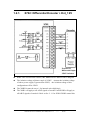
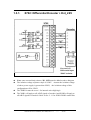
The block diagram of X702 with differential encoder is given as follows:
z
z
z
z
z
z
z
X702 can be plugged into 7188XB or 7188EX.
X702 equips a isolated 5V power for 5V encoder.
Refer to Sec. 1.2 for 12V encoder & Sec. 1.3 for 24V encoder.
(A1+,A1-)(B1+,B1-)(Z1+, Z1-) is for encoder1 and
(A2+,A2-)(B2+,B2-)(Z2+,Z2-) is for encoder2.
These signals are connected to photo-couple devices for signal isolation.
The internal logic is active high.
The Z1 after XOR1 logic is connected to int0 of I/O Expansion Bus
The Z2 after XOR2 logic is connected to int1 of I/O Expansion Bus
Both int0 & int1 are initial low & active high.
Refer to Sec. 3.1.3 for more information
For differential encoder
(A1+,A1-)(B1+,B1-)(Z1+,Z1-) are active high, XOR1/XOR2 must be set to 1.
Refer to Sec. 1.1.1, Sec. 1.1.3, Sec. 1.2.1, Sec. 1.3.1 for more information about
this configuration, X702+differential encoder.
X702/X703 User’s Manual, Nov/2004, Rev. 1.0
------
5/59
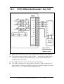
The block diagram of X702 with single-ended encoder is given as follows:
z
z
For single-ended encoder
If (A,B,Z) is active low, XOR1/XOR2 must be set to 1
If (A,B,Z) is active high, XOR1/XOR2 must be set to 0
Refer to Sec. 1.1.2, Sec. 1.1.4, Sec. 1.2.2, Sec. 1.3.2 for more information about
this configuration, X702+single-ended encoder
X702/X703 User’s Manual, Nov/2004, Rev. 1.0
------
6/59
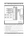
The block diagram of X703 is given as follows:
z
z
z
z
z
X703 can be plugged into 7188XB or 7188EX.
X703 equips a isolated 5V power for 5V encoder.
Refer to Sec. 1.2 for 12V encoder & Sec. 1.3 for 24V encoder.
(VCOM1+,A1,B1,Z1) is for encoder1, (VCOM2+, A2,B2,Z2) is for encoder2
and (VCOM3+,A3,B3,Z3)is for encoder3.
These signals are connected to photo-couple devices for signal isolation.
The internal logic is active high.
If (VCOM1,A1,B1,Z1) is active high, XOR1 must be set to 0
If (VCOM1,A1,B1,Z1) is active low, XOR1 must be set to 1
If (VCOM2+,A2,B2,Z2) is active high, XOR2 must be set to 0
If (VCOM2+,A2,B2,Z2) is active low, XOR2 must be set to 1
If (VCOM3+,A3,B3,Z3) is active high, XOR3 must be set to 0
If (VCOM3+,A3,B3,Z3) is active low, XOR3 must be set to 1
The Z1 after XOR1 logic is connected to int0 of I/O Expansion Bus
The Z2 after XOR2 logic is connected to int1 of I/O Expansion Bus
The Z3 after XOR3 logic is connected to int1 of I/O Expansion Bus
Refer to Sec. 3.2.3 for more information
X702/X703 User’s Manual, Nov/2004, Rev. 1.0
------
7/59
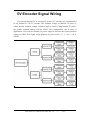
5V Encoder Signal Wiring
User can use internal 5V or external 5V to drive 5V encoder. It is recommended
to use internal 5V for 5V encoder. The isolation voltage of internal 5V power is
1000V and the isolation voltage of photo-couple is 2500V. Using internal 5V power,
the system isolation voltage will be 1000V. This configuration can fit most of
applications. User can use external 5V power supply to increase the system isolation
voltage to 2500V. The signal wiring diagram are given in Sec. 1.1.1 ~ Sec. 1.1.8 as
follows:
X702/X703 User’s Manual, Nov/2004, Rev. 1.0
------
8/59
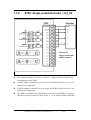
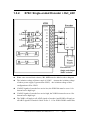
1.1.1.
X702: Differential Encoder & Int_5V
Internal 5V
Differential input
1000V isolation
z
z
z
The isolation voltage of 5V power is 1000V. So the isolation voltage of this
configuration is also 1000V.
The XOR2 bit must be set to 1 for internal active high logic
The XOR1 will apply to all A/B/Z signals of encoder1 and XOR2 will apply to
all A/B/Z signals of encoder2. Refer to Sec. 2.1.1 for XOR1/XOR2 control bits
X702/X703 User’s Manual, Nov/2004, Rev. 1.0
------
9/59
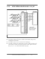
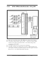
1.1.2.
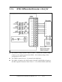
X702: Single-ended Encoder + Int_5V
Internal 5V
Single-ended input
1000V isolation
z
z
z
z
The isolation voltage of 5V power is 1000V. So the isolation voltage of this
configuration is also 1000V.
If A/B/Z signals of encoder2 are active low, the XOR2 bit must be set to 1 for
internal active high logic
If A/B/Z signals of encoder2 are active high, the XOR2 bit must be set to 0 for
internal active high logic
The XOR1 will apply to all A/B/Z signals of encoder1 and XOR2 will apply to
all A/B/Z signals of encoder2. Refer to Sec. 2.1.1 for XOR1/XOR2 control bits
X702/X703 User’s Manual, Nov/2004, Rev. 1.0
------
10/59
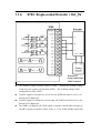
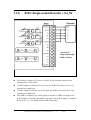
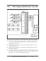
1.1.3.
X702: Differential Encoder + Ext_5V
External 5V
Differential input
2500V isolation
z
z
z
The isolation voltage of photo-couple is 2500V. Assume the isolation voltage
of above power supply is greater than 2500V, the isolation voltage of this
configuration will be 2500V.
The XOR2 bit must be set to 1 for internal active high logic
The XOR1 will apply to all A/B/Z signals of encoder1 and XOR2 will apply to
all A/B/Z signals of encoder2. Refer to Sec. 2.1.1 for XOR1/XOR2 control bits
X702/X703 User’s Manual, Nov/2004, Rev. 1.0
------
11/59
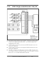
1.1.4.
X702: Single-ended Encoder + Ext_5V
External 5V
Single-ended input
2500V isolation
z
z
z
z
The isolation voltage of photo-couple is 2500V. Assume the isolation voltage
of above power supply is greater than 2500V, the isolation voltage of this
configuration will be 2500V.
If A/B/Z signals of encoder2 are active low, the XOR2 bit must be set to 1 for
internal active high logic
If A/B/Z signals of encoder2 are active high, the XOR2 bit must be set to 0 for
internal active high logic
The XOR1 will apply to all A/B/Z signals of encoder1 and XOR2 will apply to
all A/B/Z signals of encoder2. Refer to Sec. 2.1.1 for XOR1/XOR2 control bits
X702/X703 User’s Manual, Nov/2004, Rev. 1.0
------
12/59
1.1.5.
X703: Differential Encoder + Int_5V
Internal 5V
Differential input
1000V isolation
z
z
z
The isolation voltage of 5V power is 1000V. So the isolation voltage of this
configuration is also 1000V.
The XOR3 bit must be set to 0 for internal active high logic
The XOR1 will apply to all A/B/Z signals of encoder1, XOR2 will apply to all
A/B/Z signals of encoder2 and XOR3 will apply to A/B/Z signals of encoder3.
Refer to Sec. 2.2.1 for XOR1/XOR2/XOR3 control bits
X702/X703 User’s Manual, Nov/2004, Rev. 1.0
------
13/59
1.1.6.
X703: Single-ended Encoder + Int_5V
Internal 5V
Single-ended input
1000V isolation
z
z
z
z
The isolation voltage of 5V power is 1000V. So the isolation voltage of this
configuration is also 1000V.
If A/B/Z signals of encoder3 are active low, the XOR3 bit must be set to 1 for
internal active high logic
If A/B/Z signals of encoder3 are active high, the XOR3 bit must be set to 0 for
internal active high logic
The XOR1 will apply to all A/B/Z signals of encoder1, XOR2 will apply to all
A/B/Z signals of encoder2 and XOR3 will apply to all A/B/Z signals of encoder3.
Refer to Sec. 2.2.1 for XOR1/XOR2/XOR3 control bits
X702/X703 User’s Manual, Nov/2004, Rev. 1.0
------
14/59
1.1.7.
X703: Differential Encoder + Ext_5V
External 5V
Differential input
2500V isolation
z
z
z
The isolation voltage of photo-couple is 2500V. Assume the isolation voltage
of above power supply is greater than 2500V, the isolation voltage of this
configuration will be 2500V.
The XOR3 bit must be set to 0 for internal active high logic
The XOR1 will apply to all A/B/Z signals of encoder1, XOR2 will apply to all
A/B/Z signals of encoder2 and XOR3 will apply to all A/B/Z signals of encoder3.
Refer to Sec. 2.2.1 for XOR1/XOR2/XOR3 control bits
X702/X703 User’s Manual, Nov/2004, Rev. 1.0
------
15/59
1.1.8.
X703: Single-ended Encoder + Ext_5V
External 5V
Single-ended input
2500V isolation
z
z
z
z
The isolation voltage of photo-couple is 2500V. Assume the isolation voltage
of above power supply is greater than 2500V, the isolation voltage of this
configuration will be 2500V.
If A/B/Z signals of encoder3 are active low, the XOR3 bit must be set to 1 for
internal active high logic
If A/B/Z signals of encoder3 are active high, the XOR3 bit must be set to 0 for
internal active high logic
The XOR1 will apply to all A/B/Z signals of encoder1, XOR2 will apply to all
A/B/Z signals of encoder2 and XOR3 will apply to all A/B/Z signals of encoder3.
Refer to Sec. 2.2.1 for XOR1/XOR2/XOR3 control bits
X702/X703 User’s Manual, Nov/2004, Rev. 1.0
------
16/59
1.2.
12V Encoder Signal
The internal logic of X702/X703 is designed for 5V logic. A current limit resistor
must be added to X702/X703 for 12V encoder. The signal wiring diagram are given in
Sec. 1.2.1 ~ Sec. 1.2.4 as follows:
X702/X703 User’s Manual, Nov/2004, Rev. 1.0
------
17/59
1.2.1.
X702: Differential Encoder + Ext_12V
External 5V
Differential input
2500V isolation
z
z
z
z
Note: some current limit resistors, 1K, 1/4W must be added as above diagram
The isolation voltage of photo-couple is 2500V. Assume the isolation voltage
of above power supply is greater than 2500V, the isolation voltage of this
configuration will be 2500V.
The XOR2 bit must be set to 1 for internal active high logic
The XOR1 will apply to all A/B/Z signals of encoder1 and XOR2 will apply to
all A/B/Z signals of encoder2. Refer to Sec. 2.1.1 for XOR1/XOR2 control bits
X702/X703 User’s Manual, Nov/2004, Rev. 1.0
------
18/59
1.2.2.
X702: Single-ended Encoder + Ext_12V
External 12V
Single-ended input
2500V isolation
z
z
z
z
z
Note: some current limit resistors, 1K, 1/4W must be added as above diagram
The isolation voltage of photo-couple is 2500V. Assume the isolation voltage
of above power supply is greater than 2500V, the isolation voltage of this
configuration will be 2500V.
If A/B/Z signals of encoder2 are active low, the XOR2 bit must be set to 1 for
internal active high logic
If A/B/Z signals of encoder2 are active high, the XOR2 bit must be set to 0 for
internal active high logic
The XOR1 will apply to all A/B/Z signals of encoder1 and XOR2 will apply to
all A/B/Z signals of encoder2. Refer to Sec. 2.1.1 for XOR1/XOR2 control bits
X702/X703 User’s Manual, Nov/2004, Rev. 1.0
------
19/59
1.2.3.
X703: Differential Encoder + Ext_12V
External 12V
Differential input
2500V isolation
z
z
z
z
Note: some current limit resistors, 1K, 1/4W must be added as above diagram
The isolation voltage of photo-couple is 2500V. Assume the isolation voltage
of above power supply is greater than 2500V, the isolation voltage of this
configuration will be 2500V.
The XOR3 bit must be set to 0 for internal active high logic
The XOR1 will apply to all A/B/Z signals of encoder1, XOR2 will apply to all
A/B/Z signals of encoder2 and XOR3 will apply to all A/B/Z signals of encoder3.
Refer to Sec. 2.2.1 for XOR1/XOR2/XOR3 control bits
X702/X703 User’s Manual, Nov/2004, Rev. 1.0
------
20/59
1.2.4.
X703: Single-ended Encoder + Ext_12V
External 12V
Single-ended input
2500V isolation
z
z
z
z
z
Note: some current limit resistors, 1K, 1/4W must be added as above diagram
The isolation voltage of photo-couple is 2500V. Assume the isolation voltage
of above power supply is greater than 2500V, the isolation voltage of this
configuration will be 2500V.
If A/B/Z signals of encoder3 are active low, the XOR3 bit must be set to 1 for
internal active high logic
If A/B/Z signals of encoder3 are active high, the XOR3 bit must be set to 0 for
internal active high logic
The XOR1 will apply to all A/B/Z signals of encoder1, XOR2 will apply to all
A/B/Z signals of encoder2 and XOR3 will apply to all A/B/Z signals of encoder3.
Refer to Sec. 2.2.1 for XOR1/XOR2/XOR3 control bits
X702/X703 User’s Manual, Nov/2004, Rev. 1.0
------
21/59
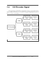
1.3.
24V Encoder Signal
The internal logic of X702/X703 is designed for 5V logic. A current limit resistor
must be added to X702/X703 for 24V encoder. The signal wiring diagram are given in
Sec. 1.3.1 ~ Sec. 1.3.4 as follows:
X702/X703 User’s Manual, Nov/2004, Rev. 1.0
------
22/59
1.3.1.
X702: Differential Encoder + Ext_24V
External 24V
Differential input
2500V isolation
z
z
z
z
Note: some current limit resistors, 2K, 1/2W must be added as above diagram
The isolation voltage of photo-couple is 2500V. Assume the isolation voltage
of above power supply is greater than 2500V, the isolation voltage of this
configuration will be 2500V.
The XOR2 bit must be set to 1 for internal active high logic
The XOR1 will apply to all A/B/Z signals of encoder1 and XOR2 will apply to
all A/B/Z signals of encoder2. Refer to Sec. 2.1.1 for XOR1/XOR2 control bits
X702/X703 User’s Manual, Nov/2004, Rev. 1.0
------
23/59
1.3.2.
X702: Single-ended Encoder + Ext_24V
External 24V
Single-ended input
2500V isolation
z
z
z
z
z
Note: some current limit resistors, 2K, 1/2W must be added as above diagram
The isolation voltage of photo-couple is 2500V. Assume the isolation voltage
of above power supply is greater than 2500V, the isolation voltage of this
configuration will be 2500V.
If A/B/Z signals of encoder2 are active low, the XOR2 bit must be set to 1 for
internal active high logic
If A/B/Z signals of encoder2 are active high, the XOR2 bit must be set to 0 for
internal active high logic
The XOR1 will apply to all A/B/Z signals of encoder1 and XOR2 will apply to
all A/B/Z signals of encoder2. Refer to Sec. 2.1.1 for XOR1/XOR2 control bits
X702/X703 User’s Manual, Nov/2004, Rev. 1.0
------
24/59
1.3.3.
X703: Differential Encoder + Ext_24V
:
External 24V
Differential input
2500V isolation
z
z
z
z
Note: some current limit resistors, 2K, 1/2W must be added as above diagram
The isolation voltage of photo-couple is 2500V. Assume the isolation voltage
of above power supply is greater than 2500V, the isolation voltage of this
configuration will be 2500V.
The XOR3 bit must be set to 0 for internal active high logic
The XOR1 will apply to all A/B/Z signals of encoder1, XOR2 will apply to all
A/B/Z signals of encoder2 and XOR3 will apply to all A/B/Z signals of encoder3.
Refer to Sec. 2.2.1 for XOR1/XOR2/XOR3 control bits
X702/X703 User’s Manual, Nov/2004, Rev. 1.0
------
25/59
1.3.4.
X703: Single-ended Encoder + Ext_24V
External 24V
Single-ended input
2500V isolation
z
z
z
z
z
Note: some current limit resistors, 2K, 1/2W must be added as above diagram
The isolation voltage of photo-couple is 2500V. Assume the isolation voltage
of above power supply is greater than 2500V, the isolation voltage of this
configuration will be 2500V.
If A/B/Z signals of encoder3 are active low, the XOR3 bit must be set to 1 for
internal active high logic
If A/B/Z signals of encoder3 are active high, the XOR3 bit must be set to 0 for
internal active high logic
The XOR1 will apply to all A/B/Z signals of encoder1, XOR2 will apply to all
A/B/Z signals of encoder2 and XOR3 will apply to all A/B/Z signals of encoder3.
Refer to Sec. 2.2.1 for XOR1/XOR2/XOR3 control bits
X702/X703 User’s Manual, Nov/2004, Rev. 1.0
------
26/59
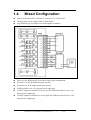
1.4.
Mixed Configuration
z
z
z
power can be internal 5V, external 5V, extern 12V or external 24V
encoder signal can be single-ended or differential
Any different type of encoders can used together as follows:
z
z
z
z
z
There are two different type of encoders used in this configuration.
Encoder1 is a 24V & differential type encoder
Encoder2 is a 5V & single-ended type encoder
XOR1 must be set to 1 for internal active high logic
If A/B/Z signals of encoder2 are active low, the XOR2 bit must be set to 1 for
internal active high logic
If A/B/Z signals of encoder2 are active high, the XOR2 bit must be set to 0 for
internal active high logic
z
X702/X703 User’s Manual, Nov/2004, Rev. 1.0
------
27/59
z
z
z
z
z
z
z
z
z
There are three different type of encoders used in this configuration
Encoder1 is a 24V & differential type encoder
Encoder2 is a 12V & single-ended type encoder
Encoder3 is a 5V & single-ended type encoder
XOR1 must be set to 1 for internal active high logic
If A/B/Z signals of encoder2 are active low, the XOR2 bit must be set to 1 for
internal active high logic
If A/B/Z signals of encoder2 are active high, the XOR2 bit must be set to 0 for
internal active high logic
If A/B/Z signals of encoder3 are active low, the XOR3 bit must be set to 1 for
internal active high logic
If A/B/Z signals of encoder3 are active high, the XOR3 bit must be set to 0 for
internal active high logic
X702/X703 User’s Manual, Nov/2004, Rev. 1.0
------
28/59
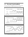
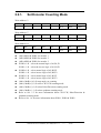
1.5. Encoder Counting Mode
The internal counting logic is active high. Refer to Sec. 1.6 to use XOR control bits
for active high logic. There are 3 different counting modes given as follows:
X702/X703 User’s Manual, Nov/2004, Rev. 1.0
------
29/59
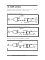
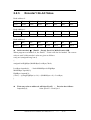
1.6. XOR Control
The expected waveform of internal logic is active high as given in Sec. 1.5. User can
use XOR control bits to select the proper waveform as follows:
Case 1: differential input of X702, set XOR=1
Case 2: active high single-ended input of X702/X703, set XOR=0
Case3: active low single-ended input of X702/X703, set XOR=1
X702/X703 User’s Manual, Nov/2004, Rev. 1.0
------
30/59
The demo program, X702XOR.EXE, is design for X702 and X703XOR.EXE is
designed for X703. User can run X702XOR.EXE or X703XOR.EXE first to check
the initial value must be 0 as follows:
1.
2.
3.
4.
Run X702XOR.EXE
Press 1
Press 1
Press Any Key to Stop
User set XOR1=1
User set XOR2=1
Initial=0
Initial=0
Note: user can set XOR1/XOR2 to 0/0, 0/1, 1/0 or 1/1. The key point is Æ all ABZ
signals must be initial 0 & active high.
X702/X703 User’s Manual, Nov/2004, Rev. 1.0
------
31/59
1. Run X703XOR.EXE
2. Press 1
3. Press 1
4. Press 1
5. Press Any Key to Stop
Initial=0
User set XOR1=1
User set XOR2=1
User set XOR3=1
Initial=0
Initial=0
Note: user can set XOR1/XOR2/XOR3 to 0/0/0, 0/0/1, 0/1/0, 0/1/1,1/0/0,1/0/1,1/1/0
or 1/1/1. The key point is Æ all ABZ signals must be initial 0 & active high.
X702/X703 User’s Manual, Nov/2004, Rev. 1.0
------
32/59
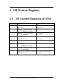
2. I/O Control Register
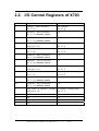
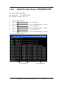
2.1. I/O Control Registers of X702
I/O Address
Read
Write
0
Read bit7 ~ bit0 of encoder1
(Sec. 2.1.3)
Clear encoder1
(Sec. 2.1.3)
1
Read bit15 ~ bit8 of encoder1
N/A
(Sec. 2.1.3) (latch by read 0)
2
Read bit23 ~ bit16 of encoder1
(Sec. 2.1.3) (no latch)
Clear encoder2
(Sec. 2.1.4)
3
Read A/B/Z & encoder1 counting Set encoder1 counting mode
mode. (Sec. 2.1.2)
(Sec. 2.1.1)
4
Read bit7 ~ bit0 of encoder2
(Sec. 2.1.4)
N/A
5
Read bit15 ~ bit8 of encoder2
N/A
(Sec. 2.1.4) (latch by read 4)
6
Read bit23 ~ bit16 of encoder2
N/A
(Sec. 2.1.4) (no latch))
7
Read A/B/Z & encoder2 counting Set encoder2 counting mode
mode. (Sec. 2.1.2)
(Sec. 2.1.1)
X702/X703 User’s Manual, Nov/2004, Rev. 1.0
------
33/59
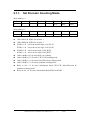
2.1.1. Set Encoder Counting Mode
Write address=3
Bit7
Bit6
Bit5
Bit4
Bit3
Bit2
Bit1
Bit0
0
0
0
0
0
M1A
M1B
XOR1
Write address=7
Bit7
Bit6
Bit5
Bit4
Bit3
Bit2
Bit1
Bit0
0
0
0
0
0
M2A
M2B
XOR2
z
z
z
z
z
z
z
z
z
z
(M1A,M1B) & XOR1 for encoder 1
(M2A,M2B) & XOR2 for encoder 2
XOR1=0 Æ select the normal logic of A1,B1,Z1
XOR1=1 Æ select the inverse logic of A1,B1,Z1
XOR2=0 Æ select normal logic of A2,B2,Z2
XOR2=1 Æ select inverse logic of A2,B2,Z2
(MxA, MxB)=(0,0) Æ stop mode, no counting
(MxA, MxB)=(0,1) Æ select CW/CCW counting mode
(MxA, MxB)=(1,0) Æ select Pulse/Direction counting mode
(MxA, MxB)=(1,1) Æ select quadrant counting mode
Refer to Sec. 1.5 for more information about CW/CCW, Pulse/Direction &
quadrant counting mode
Refer to Sec. 1.6 for more information about XOR1 & XOR2
X702/X703 User’s Manual, Nov/2004, Rev. 1.0
------
34/59
2.1.2. Read A/B/Z & Encoder Counting Mode
Read address=3
Bit7
Bit6
Bit5
Bit4
Bit3
Bit2
Bit1
Bit0
0
0
Z1
B1
A1
M1A
M1B
XOR1
Read address=7
Bit7
Bit6
Bit5
Bit4
Bit3
Bit2
Bit1
Bit0
0
0
Z2
B2
A2
M2A
M2B
XOR2
z
z
z
(Z1,B1,A1) is the logic status after XOR1, must be active high
(Z2,B2,A2) is the logic status after XOR2, must be active high
Refer to Sec. 2.1.1 for more information about MxA, MxB, XORx
z
Refer to Sec. 1.5 for more information about CW/CCW, Pulse/Direction &
quadrant counting mode
Refer to Sec. 1.6 for more information about XOR1, XOR2 & XOR3
z
X702/X703 User’s Manual, Nov/2004, Rev. 1.0
------
35/59
2.1.3. Encoder1 24-bit Value
Read address=0
Bit7
Bit6
Bit5
Bit4
Bit3
Bit2
Bit1
Bit0
ENA7
ENA6
ENA5
ENA4
ENA3
ENA2
ENA1
ENA0
Read Address=1
Bit7
Bit6
Bit5
Bit4
Bit3
Bit2
Bit1
Bit0
ENA15
ENA14
ENA13
ENA12
ENA11
ENA10
ENA9
ENA8
Read address=2
Bit7
Bit6
Bit5
Bit4
Bit3
Bit2
Bit1
Bit0
ENA23
ENA22
ENA21
ENA20
ENA19
ENA18
ENA17
ENA16
z 24-bit encoder1 Æ [EnA23 ~ EnA0], EnA23 is MSB, EnA0 is LSB
When program read address 0, the ENA15 ~ ENA8 will also be latched, but ENA23 ~
ENA16 will not be latched. The correct codes to read 24-bit encoder1 value are given
as follows:
read_enc1(unsigned long *enc1)
{
unsigned int HighByte,MiddleByte,LowByte,Check;
HighByte=inportb(2); // no latch
try_again:
LowByte=inportb(0); // latch MiddleByte
MiddleByte=inportb(1);
Check=inportb(2); // no latch
if (Check !=HighByte) // HighByte is changed
{
HighByte=Check;
goto try_again;
}
(*enc1) = (((long)HighByte)<<16) + (MiddleByte<<8) + LowByte;
}
z
Write any value to address 0 will clear EnA23 ~ EnA0 to 0 as follows:
Outportb(0,0);
//clear [EnA23 ~ EnA0] to 0
X702/X703 User’s Manual, Nov/2004, Rev. 1.0
------
36/59
2.1.4. Encoder2 24-bit Value
Read address=4
Bit7
Bit6
Bit5
Bit4
Bit3
Bit2
Bit1
Bit0
ENB7
ENB6
ENB5
ENB4
ENB3
ENB2
ENB1
ENB0
Read address=5
Bit7
Bit6
Bit5
Bit4
Bit3
Bit2
Bit1
Bit0
ENB15
ENB14
ENB13
ENB12
ENB11
ENB10
ENB9
ENB8
Read address=6
Bit7
Bit6
Bit5
Bit4
Bit3
Bit2
Bit1
Bit0
ENB23
ENB22
ENB21
ENB20
ENB19
ENB18
ENB17
ENB16
z 24-bit encoder2 Æ [EnB23 ~ EnB0], EnB23 is MSB, EnB0 is LSB
When program read address 4, the ENB15 ~ ENB8 will also be latched, but ENB23 ~
ENB16 will not be latched. The correct codes to read 24-bit encoder2 value are given
as follows:
read_enc2(unsigned long *enc2)
{
unsigned int HighByte,MiddleByte,LowByte,Check;
HighByte=inportb(6); // no latch
try_again2:
LowByte=inportb(4); // latch MiddleByte
MiddleByte=inportb(5);
Check=inportb(6); // no latch
if (Check !=HighByte) // HighByte is changed
{
HighByte=Check;
goto try_again2;
}
(*enc2) = (((long)HighByte)<<16) + (MiddleByte<<8) + LowByte;
}
z
Write any value to address 4 will clear EnB23 ~ EnB0 to 0 as follows:
Outportb(0,0);
//clear [EnB23 ~ EnB0] to 0
X702/X703 User’s Manual, Nov/2004, Rev. 1.0
------
37/59
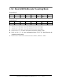
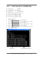
2.2. I/O Control Registers of X703
I/O Address
Read
Write
0
Read bit7 ~ bit0 of encoder1
(Sec. 2.2.3)
Clear encoder1
(Sec. 2.2.3)
1
Read bit15 ~ bit8 of encoder1
N/A
(Sec. 2.2.3), (latch by read 0)
2
Read bit23 ~ bit16 of encoder1
N/A
(Sec. 2.2.3), (latch by read 0)
3
Read A/B/Z & encoder1 counting Set encoder1 counting mode
mode (Sec 2.2.2)
(Sec. 2.2.1)
4
Read bit7 ~ bit0 of encoder2
Clear encoder2
(Sec. 2.2.4)
(Sec. 2.2.4)
Read bit15 ~ bit8 of encoder2
N/A
5
(Sec. 2.2.4), (latch by read 4)
6
Read bit23 ~ bit16 of encoder2
N/A
(Sec. 2.2.4), (latch by read 4)
7
Read A/B/Z & encoder2 counting Set encoder2 counting m mode
mode (Sec 2.2.2)
(Sec. 2.2.1)
8
Read bit7 ~ bit0 of encoder3
(Sec. 2.2.5)
Clear encoder3
(Sec. 2.2.5)
9
Read bit15 ~ bit8 of encoder3
N/A
(Sec. 2.2.5), (latch by read 8)
10
Read bit23 ~ bit16 of encoder3
N/A
(Sec. 2.2.5), (latch by read 8)
11
Read A/B/Z & encoder3 counting Set encoder3 counting mode
mode (Sec 2.2.2)
(Sec. 2.2.1)
12
N/A
N/A
13
N/A
N/A
14
N/A
N/A
15
N/A
N/A
X702/X703 User’s Manual, Nov/2004, Rev. 1.0
------
38/59
2.2.1.
Set Encoder Counting Mode
Write address=3
Bit7
Bit6
Bit5
Bit4
Bit3
Bit2
Bit1
Bit0
0
0
0
0
0
M1A
M1B
XOR1
Write address=7
Bit7
Bit6
Bit5
Bit4
Bit3
Bit2
Bit1
Bit0
0
0
0
0
0
M2A
M2B
XOR2
Write address=11
Bit7
Bit6
Bit5
Bit4
Bit3
Bit2
Bit1
Bit0
0
0
0
0
0
M3A
M3B
XOR3
z
z
z
z
z
z
z
z
z
z
z
z
(M1A,M1B) & XOR1 for encoder 1
(M2A,M2B) & XOR2 for encoder 2
(M2A,M2B) & XOR2 for encoder 2
XOR1=0 Æ select the normal logic of A1,B1,Z1
XOR1=1 Æ select the inverse logic of A1,B1,Z1
XOR2=0 Æ select normal logic of A2,B2,Z2
XOR2=1 Æ select inverse logic of A2,B2,Z2
XOR3=0 Æ select normal logic of A3,B3,Z3
XOR3=1 Æ select inverse logic of A3,B3,Z3
(MxA, MxB)=(0,0) Æ stop mode, no counting
(MxA, MxB)=(0,1) Æ select CW/CCW counting mode
(MxA, MxB)=(1,0) Æ select Pulse/Direction counting mode
(MxA, MxB)=(1,1) Æ select quadrant counting mode
Refer to Sec. 1.5 for more information about CW/CCW, Pulse/Direction &
quadrant counting mode
Refer to Sec. 1.6 for more information about XOR1, XOR2 & XOR3
X702/X703 User’s Manual, Nov/2004, Rev. 1.0
------
39/59
2.2.2.
Read A/B/Z & Encoder Counting Mode
Read address=3
Bit7
Bit6
Bit5
Bit4
Bit3
Bit2
Bit1
Bit0
0
0
Z1
B1
A1
M1A
M1B
XOR1
Read address=7
Bit7
Bit6
Bit5
Bit4
Bit3
Bit2
Bit1
Bit0
0
0
Z2
B2
A2
M2A
M2B
XOR2
Read address=11
Bit7
Bit6
Bit5
Bit4
Bit3
Bit2
Bit1
Bit0
0
0
Z3
B3
A3
M3A
M3B
XOR3
z
z
z
z
z
z
(Z1,B1,A1) is the logic status after XOR1, must be active high
(Z2,B2,A2) is the logic status after XOR2, must be active high
(Z3,B3,A3) is the logic status after XOR3, must be active high
Refer to Sec. 2.2.1 for more information about MxA, MxB, XORx
Refer to Sec. 1.5 for more information about CW/CCW, Pulse/Direction &
quadrant counting mode
Refer to Sec. 1.6 for more information about XOR1, XOR2 & XOR3
X702/X703 User’s Manual, Nov/2004, Rev. 1.0
------
40/59
2.2.3.
Encoder1 24–bit Value
Read address=0
Bit7
Bit6
Bit5
Bit4
Bit3
Bit2
Bit1
Bit0
EnA7
EnA6
EnA5
EnA4
EnA3
EnA2
EnA1
EnA0
Read Address=1
Bit7
Bit6
Bit5
Bit4
Bit3
Bit2
Bit1
Bit0
EnA15
EnA14
EnA13
EnA12
EnA11
EnA10
EnA9
EnA8
Read address=2
Bit7
Bit6
Bit5
Bit4
Bit3
Bit2
Bit1
Bit0
EnA23
EnA22
EnA21
EnA20
EnA19
EnA18
EnA17
EnA16
z 24-bit encoder1 Æ [EnA23 ~ EnA0], EnA23 is MSB, EnA0 is LSB
When program read address 0, the EnA23 ~ EnA8 will also be latched. The correct
codes to read 24-bit encoder1 value are given as follows:
read_enc1(unsigned long *enc1)
{
unsigned int HighByte,MiddleByte,LowByte,Check;
LowByte=inportb(0); // latch MiddleByte & HighByte
MiddleByte=inportb(1);
HighByte=inportb(2);
(*enc1) = (((long)HighByte)<<16) + (MiddleByte<<8) + LowByte;
}
z
Write any value to address 0 will clear EnA23 ~ EnA0 to 0 as follows:
Outportb(0,0);
//clear [EnA23 ~ EnA0] to 0
X702/X703 User’s Manual, Nov/2004, Rev. 1.0
------
41/59
2.2.4.
Encoder2 24–bit Value
Read address=4
Bit7
Bit6
Bit5
Bit4
Bit3
Bit2
Bit1
Bit0
EnB7
EnB6
EnB5
EnB4
EnB3
EnB2
EnB1
EnB0
Read Address=5
Bit7
Bit6
Bit5
Bit4
Bit3
Bit2
Bit1
Bit0
EnB15
EnB14
EnB13
EnB12
EnB11
EnB10
EnB9
EnB8
Read address=6
Bit7
Bit6
Bit5
Bit4
Bit3
Bit2
Bit1
Bit0
EnB23
EnB22
EnB21
EnB20
EnB19
EnB18
EnB17
EnB16
z 24-bit encoder2 Æ [EnB23 ~ EnB0], EnB23 is MSB, EnB0 is LSB
When program read address 4, the EnB23 ~ EnB8 will also be latched. The correct
codes to read 24-bit encoder1 value are given as follows:
read_enc2(unsigned long *enc2)
{
unsigned int HighByte,MiddleByte,LowByte,Check;
LowByte=inportb(4); // latch MiddleByte & HighByte
MiddleByte=inportb(5);
HighByte=inportb(6);
(*enc1) = (((long)HighByte)<<16) + (MiddleByte<<8) + LowByte;
}
z
Write any value to address 4 will clear EnB23 ~ EnB0 to 0 as follows:
Outportb(4,0);
//clear [EnB23 ~ EnB0] to 0
X702/X703 User’s Manual, Nov/2004, Rev. 1.0
------
42/59
2.2.5.
Encoder3 24–bit Value
Read address=8
Bit7
Bit6
Bit5
Bit4
Bit3
Bit2
Bit1
Bit0
EnC7
EnC6
EnC5
EnC4
EnC3
EnC2
EnC1
EnC0
Read Address=9++
Bit7
Bit6
Bit5
Bit4
Bit3
Bit2
Bit1
Bit0
EnC15
EnC14
EnC13
EnC12
EnC11
EnC10
EnC9
EnC8
Read address=10
Bit7
Bit6
Bit5
Bit4
Bit3
Bit2
Bit1
Bit0
EnC23
EnC22
EnC21
EnC20
EnC19
EnC18
EnC17
EnC16
z 24-bit encoder3 Æ [EnC23 ~ EnC0], EnC23 is MSB, EnC0 is LSB
When program read address 8, the EnC23 ~ EnC8 will also be latched. The correct
codes to read 24-bit encoder1 value are given as follows:
read_enc3(unsigned long *enc3)
{
unsigned int HighByte,MiddleByte,LowByte,Check;
LowByte=inportb(8); // latch MiddleByte & HighByte
MiddleByte=inportb(9);
HighByte=inportb(10);
(*enc3) = (((long)HighByte)<<16) + (MiddleByte<<8) + LowByte;
}
z
Write any value to address 8 will clear EnC23 ~ EnC0 to 0 as follows:
Outportb(8,0);
//clear [EnC23 ~ EnC0] to 0
X702/X703 User’s Manual, Nov/2004, Rev. 1.0
------
43/59
3.
Software Examples
The demo program of X702/X703 are given in the companion CD as follows:
User’s manual : CD\Napdos\7188x\manual\hardware\x702x703.pdf
User can download these demo programs from our web site as follows:
User’smanual : ftp.icpdas.com/pub/cd/8000cd/napdos/7188x/hardware/X702X703.pdf
All demo program are coded as follows:
z Using BC, Large model
z Using 7188EL.LIB
z Main program Æ MAIN.C
z One project file for BC
z One execution file
X702/X703 User’s Manual, Nov/2004, Rev. 1.0
------
44/59
3.1.
X702 Demo Program
3.1.1.
Read A/B/Z Demo, X702XOR.EXE
z Main program Æ MAIN.C
z Project file Æ X702XOR.PRJ
#include <stdio.h>
#include <stdlib.h>
#include "..\..\lib\7188E.h"
int xor1,xor2;
main()
{
Print("\nxor1 = (0 or 1) ?");
xor1=Getch()-'0'; if (xor1) xor1=1;
Print("\nxor2 = (0 or 1) ?");
xor2=Getch()-'0'; if (xor2) xor2=1;
outportb(3,xor1); // set xor1 & counting mode1=stop
outportb(7,xor2); // set xor2 & counting mode2=stop
for (;;)
{
if (Kbhit())
{
Getch(); return;
}
show_abz();
DelayMs(100);
}
}
show_abz()
{
int zba1,zba2,i;
Set Xor & Counting Mode
Read ABZ status
zba1=inport(3); // read ABZ status & counting mode of encoder1
zba2=inport(7); // read ABZ status & counting mode of encoder2
X702/X703 User’s Manual, Nov/2004, Rev. 1.0
------
45/59
Print("\n(XOR1=%d, Z1B1A1=",xor1);
for (i=0; i<3; i++)
{
if (zba1&0x20) Print("1"); else Print("0");
zba1 = (zba1<<1);
}
Show ABZ status
Print(") * (XOR2=%d, Z2B2A2=",xor2);
for (i=0; i<3; i++)
{
if (zba2&0x20) Print("1"); else Print("0");
zba2 = (zba2<<1);
}
Print(")");
}
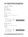
1.
2.
3.
4.
Run X702XOR.EXE
Press 1
Press 1
Press Any Key to Stop
Initial=0
User set XOR1=1
User set XOR2=1
Initial=0
X702/X703 User’s Manual, Nov/2004, Rev. 1.0
------
46/59
3.1.2.
Read Encoder Demo, X702RENC.EXE
z Main program Æ MAIN.C
z Project file
Æ X702RENC.PRJ
#include <stdio.h>
#include <stdlib.h>
#include "..\..\lib\7188E.h"
int xor1,xor2,mode1,mode2;
unsigned long EncVal1,EncVal2;
main()
{
Print("\nxor1 = (0 or 1) ?");
xor1=Getch()-'0'; if (xor1) xor1=1;
try_again1:
Print("\nmode1 = (0=stop,1=cw/ccw,2=pule/dir,3=a/b) ?");
mode1=Getch();
switch(mode1)
{
case '0' : break;
// stop
case '1' : xor1+=0x02; break;
// cw/ccw
case '2' : xor1+=0x04; break;
// pulse/dir
Set XOR1 & Counting Mode1
case '3' : xor1+=0x06; break;
// a/b
default : goto try_again1;
}
Print("\nxor2 = (0 or 1) ?");
xor2=Getch()-'0'; if (xor2) xor2=1;
try_again2:
Print("\nmode2 = (0=stop,1=cw/ccw,2=pule/dir,3=a/b) ?");
mode2=Getch();
switch(mode2)
{
case '0' : break;
// stop
case '1' : xor2+=0x02; break;
// cw/ccw
Set XOR2 & Counting Mode2
case '2' : xor2+=0x04; break;
// pulse/dir
case '3' : xor2+=0x06; break;
// a/b
default : goto try_again2;
}
X702/X703 User’s Manual, Nov/2004, Rev. 1.0
------
47/59
outportb(3,xor1); // set xor1 & counting mode1
outportb(7,xor2); // set xor2 & counting mode2
outportb(0,0); // clear encoder1 to 0
outportb(4,0); // clear encoder2 to 0
Clear encoder1 & encoder2
for (;;)
{
if (Kbhit())
{
Getch(); return;
}
read_enc1(&EncVal1);
read_enc2(&EncVal2);
Print("\n(mode1=%x,enc1=%lx)
(mode2=%x,enc2=%lx)",xor1,EncVal1,xor2,EncVal2);
DelayMs(100);
}
}
read_enc1(unsigned long *enc1)
{
unsigned int HighByte,MiddleByte,LowByte,Check;
HighByte=inportb(2); // no latch
try_again:
LowByte=inportb(0); // latch MiddleByte
MiddleByte=inportb(1);
Check=inportb(2); // no latch
if (Check !=HighByte) // HighByte is changed
{
HighByte=Check;
goto try_again;
}
(*enc1) = (((long)HighByte)<<16) + (MiddleByte<<8) + LowByte;
}
X702/X703 User’s Manual, Nov/2004, Rev. 1.0
------
48/59
Get 24-bit encoder1
read_enc2(unsigned long *enc2)
{
unsigned int HighByte,MiddleByte,LowByte,Check;
HighByte=inportb(6); // no latch
try_again:
LowByte=inportb(4); // latch MiddleByte
MiddleByte=inportb(5);
Check=inportb(6); // no latch
if (Check !=HighByte) // HighByte is changed
{
HighByte=Check;
goto try_again;
}
(*enc2) = (((long)HighByte)<<16) + (MiddleByte<<8) + LowByte;
}
1.
2.
3.
4.
5.
6.
Run X702RENC.EXE
Press 1
Press 1
Press 1
Press 1
Press Any Key to Stop
Get 24-bit encoder2
User set XOR1=1
User set counting mode1 = cw/ccw
User set XOR2=1
User set counting mode2 = cw/ccw
Initial count=0
Up counting
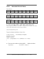
Down counting
X702/X703 User’s Manual, Nov/2004, Rev. 1.0
------
49/59
3.1.3.
z
z
z
z
z
Z Interrupt Demo, X702INT.EXE
Main program
Æ MAIN.C
Interrupt service routine Æ INT.C
Project file
Æ X702INT.PRJ
Z1 Æ to int0 of 7188Xb or 7188EX
Z2 Æ to int1 of 7188XB or 7188EX
The main.c is given as follows:
=============================================================
#include <stdio.h>
#include <stdlib.h>
#include "..\..\lib\7188E.h"
int xor1,xor2,mode1,mode2;
unsigned long EncVal1,EncVal2;
extern unsigned long EncLatch1,EncLatch2;//defined in int.c
main()
{
Print("\nxor1 = (0 or 1) ?");
xor1=Getch()-'0'; if (xor1) xor1=1;
try_again1:
Print("\nmode1 = (0=stop,1=cw/ccw,2=pule/dir,3=a/b) ?");
mode1=Getch();
switch(mode1)
{
case '0' : break;
// stop
case '1' : xor1+=0x02; break;
// cw/ccw
case '2' : xor1+=0x04; break;
// pulse/dir
case '3' : xor1+=0x06; break;
// a/b
default : goto try_again1;
}
X702/X703 User’s Manual, Nov/2004, Rev. 1.0
------
50/59
Print("\nxor2 = (0 or 1) ?");
xor2=Getch()-'0'; if (xor2) xor2=1;
try_again2:
Print("\nmode2 = (0=stop,1=cw/ccw,2=pule/dir,3=a/b) ?");
mode2=Getch();
switch(mode2)
{
case '0' : break;
// stop
case '1' : xor2+=0x02; break;
// cw/ccw
case '2' : xor2+=0x04; break;
// pulse/dir
case '3' : xor2+=0x06; break;
// a/b
default : goto try_again2;
}
outportb(3,xor1); // set xor1 & counting mode1
outportb(7,xor2); // set xor2 & counting mode2
outportb(0,0); // clear encoder1 to 0
outportb(4,0); // clear encoder2 to 0
InstallInt0Isr();
InstallInt1Isr();
for (;;)
{
if (Kbhit())
{
RestoreInt0Isr();
RestoreInt1Isr();
Getch(); return;
}
Install interrupt service routine for Z1 & Z2
read_enc1(&EncVal1);
read_enc2(&EncVal2);
Print("\n(mode1=%x,enc1=%lx)mode2=%x,enc2=%lx)"
,xor1,EncVal1,xor2,EncVal2);
Print("(Latch1=%lx,Latch2=%lx)",EncLatch1,EncLatch2);
DelayMs(100);
}
Show values latched by Z1 & Z2
}
X702/X703 User’s Manual, Nov/2004, Rev. 1.0
------
51/59
read_enc1(unsigned long *enc1)
{
unsigned int HighByte,MiddleByte,LowByte,Check;
HighByte=inportb(2); // no latch
try_again:
LowByte=inportb(0); // latch MiddleByte
MiddleByte=inportb(1);
Check=inportb(2); // no latch
if (Check !=HighByte) // HighByte is changed
{
HighByte=Check;
goto try_again;
}
(*enc1) = (((long)HighByte)<<16) + (MiddleByte<<8) + LowByte;
}
read_enc2(unsigned long *enc2)
{
unsigned int HighByte,MiddleByte,LowByte,Check;
unsigned long enc;
HighByte=inportb(6); // no latch
try_again:
LowByte=inportb(4); // latch MiddleByte
MiddleByte=inportb(5);
Check=inportb(6); // no latch
if (Check !=HighByte) // HighByte is changed
{
HighByte=Check;
goto try_again;
}
(*enc2) = (((long)HighByte)<<16) + (MiddleByte<<8) + LowByte;
}
X702/X703 User’s Manual, Nov/2004, Rev. 1.0
------
52/59
The int.c is given as follows:
=============================================================
#include <stdio.h>
#include <stdlib.h>
#include "..\..\lib\7188e.h"
#define EOITYPE_INT0
#define EOITYPE_INT1
#define INT_EOI
#define INT_MASK
0x0c
0x0d
0xff22
0xff28
// End-of-interrupt register
// Interrupt mask register
unsigned long EncLatch1,EncLatch2;
//-----------------------------------------unsigned long OldIntVect0=0,OldIntVect1=0,OldIntVect4=0;
unsigned long far *IntVect=(unsigned long far *)0L;
void interrupt Int0Isr(void)
{
Encoder1 latched by Z1
read_enc1(&EncLatch1);
outpw(INT_EOI,EOITYPE_INT0);
}
void InstallInt0Isr(void)
{
OldIntVect0=IntVect[0x0C];
// save old ISR
IntVect[0x0C]=(unsigned long)Int0Isr; // install new ISR
outpw(INT_MASK, inpw(INT_MASK)&0xffef);// enable INT-0
}
void RestoreInt0Isr(void)
{
if(OldIntVect0){
IntVect[0x0C]=OldIntVect0;
// restore OLD ISR
outpw(INT_MASK,inpw(INT_MASK)|0x0010);// disable INT-0
}
}
void interrupt Int1Isr(void)
{
read_enc2(&EncLatch2);
Encoder2 latched by Z2
outpw(INT_EOI,EOITYPE_INT1);
}
X702/X703 User’s Manual, Nov/2004, Rev. 1.0
------
53/59
void InstallInt1Isr(void)
{
OldIntVect1=IntVect[0x0D];
// save old ISR
IntVect[0x0D]=(unsigned long)Int1Isr; // install new ISR
outpw(INT_MASK, inpw(INT_MASK)&0xffdf);// enable INT-1
}
void RestoreInt1Isr(void)
{
if(OldIntVect1){
IntVect[0x0D]=OldIntVect1;
// restore OLD ISR
outpw(INT_MASK,inpw(INT_MASK)|0x0020);// disable INT-1
}
}
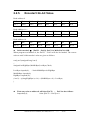
1.
2.
3.
4.
5.
6.
Run X702INT.EXE
Press 1
Press 1
Press 1
Press 1
Press Any Key to Stop
Up counting
User set XOR1=1
User set counting mode1 = cw/ccw
User set XOR2=1
User set counting mode2 = cw/ccw
Down counting
Latch by Int0
X702/X703 User’s Manual, Nov/2004, Rev. 1.0
------
Latch by Int1
54/59
3.2.
X703 Demo Program
3.2.1.
Read A/B/Z Demo, X703XOR.EXE
z
z
z
Main program Æ MAIN.C
Project file
Æ X702XOR.PRJ
MAIN.C is similar to Sec. 3.1.1.
1. Run X703XOR.EXE
2. Press 1
3. Press 1
4. Press 1
5. Press Any Key to Stop
Initial=0
User set XOR2=1
User set XOR3=1
Initial=0
Initial=0
X702/X703 User’s Manual, Nov/2004, Rev. 1.0
------
55/59
3.2.2.
Read Encoder Demo, X703RENC.EXE
z
z
z
Main program Æ MAIN.C
Project file
Æ X702RENC.PRJ
MAIN.C is similar to Sec. 3.1.2.
1.
2.
3.
4.
5.
6.
7.
Run X703RENC.EXE
Press 1
Press 1
Press 1
Press 1
Press 1
Press 1
8.
Press Any Key to Stop
Up counting
User set XOR1=1
User set counting mode1 = cw/ccw
User set XOR2=1
User set counting mode2 = cw/ccw
User set XOR3=1
User set counting mode3 = cw/ccw
Down counting
X702/X703 User’s Manual, Nov/2004, Rev. 1.0
------
56/59
Read to 0/4/8 will latch the high bytes of encoder 1/2/3 as follows:
read_enc1(unsigned long *enc1)
{
unsigned int HighByte,MiddleByte,LowByte,Check;
LowByte=inportb(0); // latch MiddleByte & HighByte
MiddleByte=inportb(1);
HighByte=inportb(2);
(*enc1) = (((long)HighByte)<<16) + (MiddleByte<<8) + LowByte;
}
read_enc2(unsigned long *enc2)
{
unsigned int HighByte,MiddleByte,LowByte,Check;
LowByte=inportb(4); // latch MiddleByte & HighByte
MiddleByte=inportb(5);
HighByte=inportb(6);
(*enc2) = (((long)HighByte)<<16) + (MiddleByte<<8) + LowByte;
}
read_enc3(unsigned long *enc3)
{
unsigned int HighByte,MiddleByte,LowByte,Check;
LowByte=inportb(8); // latch MiddleByte & HighByte
MiddleByte=inportb(9);
HighByte=inportb(10);
(*enc3) = (((long)HighByte)<<16) + (MiddleByte<<8) + LowByte;
}
X702/X703 User’s Manual, Nov/2004, Rev. 1.0
------
57/59
3.2.3.
Z Interrupt Demo, X703INT.EXE
z
z
z
z
z
z
z
Main program
Æ MAIN.C
Interrupt service routine Æ INT.C
Project file
Æ X703INT.PRJ
MAIN.C & INT.C are similar to Sec. 3.1.3.
Z1 Æ to int0 of 7188Xb or 7188EX
Z2 Æ to int1 of 7188XB or 7188EX
Z3 Æ to int4 of 7188XB or 7188EX
1.
2.
3.
Run X703INT.EXE
Press 1
Press 1
4.
5.
6.
7.
8.
Press 1
Press 1
Press 1
Press 1
Press Any Key to Stop
Encoder 1/2/3
User set XOR1=1
User set counting mode1 = cw/ccw
User set XOR2=1
User set counting mode2 = cw/ccw
User set XOR3=1
User set counting mode3 = cw/ccw
Latch encoders by Z1/Z2/Z3
X702/X703 User’s Manual, Nov/2004, Rev. 1.0
------
58/59
The interrupt service routines for Z3 are given as follows:
#define EOITYPE_INT0
#define EOITYPE_INT1
#define EOITYPE_INT4
#define INT_EOI
#define INT_MASK
0x0c
0x0d
0x10
0xff22
0xff28
// End-of-interrupt register
// Interrupt mask register
unsigned long EncLatch1,EncLatch2,EncLatch3;
//-----------------------------------------unsigned long OldIntVect0=0,OldIntVect1=0,OldIntVect4=0;
unsigned long far *IntVect=(unsigned long far *)0L;
void interrupt Int4Isr(void)
{
read_enc3(&EncLatch3);
outpw(INT_EOI,EOITYPE_INT4);
}
void InstallInt4Isr(void)
{
OldIntVect0=IntVect[0x10];
// save old ISR
IntVect[0x10]=(unsigned long)Int4Isr; // install new ISR
outpw(INT_MASK, inpw(INT_MASK)&0xfeff);// enable INT-4
}
void RestoreInt4Isr(void)
{
if(OldIntVect4){
IntVect[0x10]=OldIntVect4;
// restore OLD ISR
outpw(INT_MASK,inpw(INT_MASK)|0x0100);// disable INT-4
}
}
X702/X703 User’s Manual, Nov/2004, Rev. 1.0
------
59/59