1
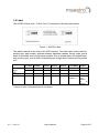
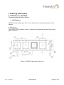
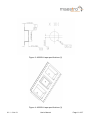
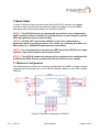
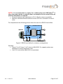
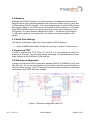
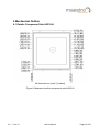
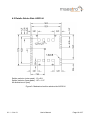
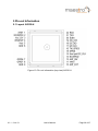
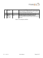
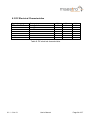
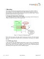
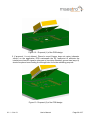
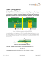
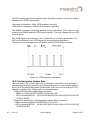
GPS Receiver A2235-H A Description of Maestro’s GPS Antenna Receiver Module A2235-H User’s Manual Version 1.1 Revision History Rev. 0.1 0.2 Date 08-15-12 04-19-13 0.9 05-08-13 1.0 1.1 08-15-13 10-16-13 Description First release 1.Update I2C interface description 2.Update Pin information 3.Add self-start description 4.Add External Antenna description 1.Version updated 2.Add section 6.1 remark Update Pin information and Table 6 current consumption data Update Pin information and Mechanical outline solder side A2235-H mm-dd-yy Written by Checked by Approval by V1.1 – Oct-13 Name Happy wen Sam Law, Matthieu Frank Tang, Calvin Yau User’s Manual Date 10-16-13 10-16-13 10-16-13 Signature HW S L,M F T,C Y Page 2 of 37 Disclaimer THIS DOCUMENT CONTAINS PROPRIETARY INFORMATION OF MAESTRO WIRELESS SOLUTIONS LIMITED. IT MAY NOT BE COPIED OR TRANSMITTED BY ANY MEANS, PASSED TO OTHERS, OR STORED IN ANY RETRIEVAL SYSTEM OR MEDIA, WITHOUT PRIOR CONSENT OF MAESTRO OR ITS AUTHORIZED AGENTS. THE INFORMATION IN THIS DOCUMENT IS, TO THE BEST OF OUR KNOWLEDGE, ENTIRELY CORRECT. HOWEVER, MAESTRO CAN NEITHER ACCEPT LIABILITY FOR ANY INACCURACIES, OR THE CONSEQUENCES THEREOF, NOR FOR ANY LIABILITY ARISING FROM THE USE OR APPLICATION OF ANY CIRCUIT, PRODUCT, OR EXAMPLE SHOWN IN THE DOCUMENT. THE PRODUCT (HARD- AND SOFTWARE) DESCRIBED IN THIS DOCUMENTATION IS NOT AUTHORIZED FOR USE IN LIFE SUPPORT DEVICES OR SYSTEMS WITHOUT THE EXPRESS WRITTEN APPROVAL OF MAESTRO. THIS DOCUMENT MAY PROVIDE LINKS TO OTHER WORLD WIDE WEB SITES OR RESOURCES. BECAUSE MAESTRO HAS NO CONTROL OVER SUCH SITES AND RESOURCES, MAESTRO SHALL NOT BE RESPONSIBLE FOR THE AVAILABILITY OF SUCH EXTERNAL SITES OR RESOURCES, AND DOES NOT ENDORSE AND IS NOT RESPONSIBLE OR LIABLE FOR ANY CONTENT, ADVERTISING, PRODUCTS, OR OTHER MATERIALS ON OR AVAILABLE FROM SUCH SITES OR RESOURCES. MAESTRO SHALL NOT BE RESPONSIBLE OR LIABLE, DIRECTLY OR INDIRECTLY, FOR ANY DAMAGE OR LOSS CAUSED OR ALLEGED TO BE CAUSED BY OR IN CONNECTION WITH USE OF OR RELIANCE ON ANY SUCH CONTENT, GOODS OR SERVICES AVAILABLE ON OR THROUGH ANY SUCH SITE OR RESOURCE. MAESTRO RESERVES THE RIGHT TO CHANGE, MODIFY, OR IMPROVE THIS DOCUMENT OR THE PRODUCT DESCRIBED HEREIN, AS SEEN FIT BY MAESTRO WITHOUT FURTHER NOTICE. V1.1 – Oct-13 User’s Manual Page 3 of 37 Table of Contents 1 Introduction ........................................................................................................ 6 1.1 Feature Overview .............................................................................................. 6 1.2 Characteristics Overview .................................................................................. 7 1.3 RoHS and Lead-Free Information ..................................................................... 7 1.4 Label ................................................................................................................. 8 1.5 Characteristics .................................................................................................. 9 1.5.1 GPS Characteristics.................................................................................................. 9 1.5.2 Mechanical Characteristics ....................................................................................... 9 1.6 Handling Precautions ........................................................................................ 9 2 Ordering Information ....................................................................................... 10 2.1 GPS Receiver A2235-H .................................................................................. 10 2.2 Packing ........................................................................................................... 10 2.3 Additional Equipment ...................................................................................... 13 3 Quick Start ........................................................................................................ 14 3.1 Minimum Configuration ................................................................................... 14 3.2 Antenna........................................................................................................... 16 3.3 Serial Port Settings ......................................................................................... 16 3.4 Improved TTFF ............................................................................................... 16 3.5 Self-start configuration .................................................................................... 16 3.6 Configure the baud rate .................................................................................. 17 4 Mechanical Outline .......................................................................................... 18 4.1 Details Component Side A2235-H .................................................................. 18 4.2 Details Solder Side A2235-H .......................................................................... 19 5 Pin-out Information .......................................................................................... 20 5.1 Layout A2235-H .............................................................................................. 20 5.2 Description A2235-H Signals .......................................................................... 21 6 Electrical Characteristics ................................................................................ 23 6.1 Operating Conditions ...................................................................................... 23 6.2 Absolute Maximum Ratings ............................................................................ 23 6.3 DC Electrical Characteristics ........................................................................... 24 7 Mounting ........................................................................................................... 25 7.1 Proposed Footprint for Soldering .................................................................... 25 7.2 PCB Design Guide .......................................................................................... 25 7.3 Recommended Profile for Reflow Soldering ................................................... 27 8 Use of External Antenna .................................................................................. 28 8.1 Connection of RF Signal ................................................................................. 28 8.2 External Antenna............................................................................................. 29 8.2.1 Recommended Parameters .................................................................................... 29 8.2.2 Hints ....................................................................................................................... 29 V1.1 – Oct-13 User’s Manual Page 4 of 37 9 Quality and Reliability...................................................................................... 30 9.1 Environmental Conditions ............................................................................... 30 9.2 Product Qualification ....................................................................................... 30 9.3 Production Test ............................................................................................... 30 10 Applications and Hints .................................................................................. 31 10.1 Initial Module Start ........................................................................................ 31 10.2 Proper Shutdown and Power-On-Reset (POR) ............................................. 31 10.3 SiRFawareTM Support ................................................................................... 31 10.4 Push-to-Fix Mode .......................................................................................... 31 10.5 Hibernate Mode............................................................................................. 32 10.6 Extended Ephemeris ..................................................................................... 32 10.7 TM_GPIO5 pin (1 pulse per second pin) ....................................................... 32 10.8 5 Hz Navigation Update Rate ........................................................................ 33 11 Evaluation Kit EVA2235-H ............................................................................. 34 12 Related Information ....................................................................................... 35 12.1 Contact .......................................................................................................... 35 12.2 Related Documents ....................................................................................... 35 12.3 Related Tools ................................................................................................ 35 13 List of Figures ................................................................................................ 36 14 List of Tables .................................................................................................. 37 V1.1 – Oct-13 User’s Manual Page 5 of 37 1 Introduction A2235-H is an antenna module with SiRF Star IV ROM based chip and an on-board patch antenna (15mm x 15mm x 4mm). It is cost down version of A2035-H with reduced size and stacked up antenna architecture. RF switch was implemented (but NOT on engineering samples) so as to support external active antenna for performance enhancement if required. In order to have an easier migration for existing customers using A2035-H, we decided to keep same pin assignment as that of A2035-H. Additional pins for supporting external antenna won’t affect this drop-in replacement property. Since there is an RF feed point underneath the module, special PCB design is required on user’s application. Receiver part of A2235-H is fully identical to A2200-A with latest CSR Premier ROM 9333 and enabling I2C host port, Host Port I2C_CLK (Pin 14) was added for this new function. The A2235-H is a module designed for a 3.3V environment. 1.1 Feature Overview The A2235-H is a new module with the following outstanding features. Fast, responsive location experience o High-sensitive navigation engine with tracking down to -163dBm o 48 track verification channels o SBAS (WAAS, EGNOS, MSAS, GAGAN) Breakthrough micro power technology o Requires only 50 – 500µA to maintain hot start capability Active jammer remover o Removes in-band jammers up to 80dB/Hz o Tracks up to eight CW (continuous wave) jammers Size: 17.8mm (L) x 16.5mm (W) x 6.7mm (H) Operating voltage: 3V3 No internal EEPROM but support external EEPROM through I2C interface Extremely low power consumption by using DC/DC converter No back-up battery required MEMS supports TCXO is used for providing stable 16.369MHz system clock CSR Premier ROM 9333 is used which is equivalent to Release 2.2 (i.e. F/W 4.1.2) Support external active antenna Build-in LNA with close to 20dB gain V1.1 – Oct-13 User’s Manual Page 6 of 37 1.2 Characteristics Overview The module’s most important characteristics are: Operable at 3.3V / 22mA @ 1fix per second UART interface at CMOS level Small form factor of 17.78 x 16.51 mm²(0.7” x 0.65”) Supported temperature range: -40°C to +85°C Single-sided SMT component, for reflow soldering RoHS compliant, lead-free Tape & reel packaging Excellent antenna support o On-module patch antenna o Antenna input for direct connection of external active antenna o RF switch to select between antennas The antenna receiver module is available as an off-the-shelf component, 100% tested and shipped in tape-and-reel packaging. 1.3 RoHS and Lead-Free Information Maestro’s products marked with the lead-free symbol either on the module or the packaging comply with the "Directive 2002/95/EC of the European Parliament and the Council on the Restriction of Use of certain Hazardous Substances in Electrical and Electronic Equipment" (RoHS). All Maestro GPS receiver modules, GPS antenna receiver module and telematics units are RoHS compliant. V1.1 – Oct-13 User’s Manual Page 7 of 37 1.4 Label The A2235-H label (size: 12.0x 4.0 mm²) contains the following information: Figure 1: A2235-H label The label is placed on the side of the GPS antenna. The data matrix code holds the product type, part number, software release, hardware release, factory code, year & week of assembly and a 6-digit serial number. Due to limited space on module label, only product type, year & week of assembly and 6-digit serial number will be printed on it. Representing Number digits (16) Example Meaning of Factory location XX 2 Product Number XXXXXXX 6 Part Number XXXX 4 Software Release XX 2 Hardware Release XX 2 Assembly Year/Week XXXX 4 Serial Number XXXXXX 6 TF A2235H Given 9333 Given 01 Given 01 Given 1211 Year=12 Week=11 000005 Increment from 000001 up to 999999 TF Example of MID#: TFA2235H933301011211000005 V1.1 – Oct-13 User’s Manual Page 8 of 37 1.5 Characteristics The module is characterized by the following parameters. 1.5.1 GPS Characteristics Channels Correlators Frequency Tracking Sensitivity On-module antenna Horizontal Position Accuracy Time To First Fix – TTFF (theoretical minimum values; values in real world may differ) 48, parallel tracking ~400,000 L1 (= 1,575 MHz) -163 dBm Stand alone Obscuration recovery (1) Hot start (2) Warm (3) Cold (4) < 2.5 m CEP (SA off) 0.1 s <1s < 35 s < 38 s Table 1: A2235-H GPS characteristics (1) (2) (3) (4) The calibrated clock of the receiver has not stopped, thus it knows precise time (to the µs level). The receiver has estimates of time/date/position and valid almanac and ephemeris data. The receiver has estimates of time/date/position and recent almanac. The receiver has no estimate of time/date/position, and no recent almanac. Note: Performance (sensitivity and TTFF) might slightly decrease below -30°C. 1.5.2 Mechanical Characteristics A2235-H Mechanical dimensions Length Width Height A2235-H Weight 17.78±0.20 mm, 0.7±0.008” 16.51±0.20 mm, 0.65±0.008” 7.11 mm, 0.28”(Max) 4.0 g, 0.14 oz Table 2: A2235-H dimensions and weight 1.6 Handling Precautions The GPS receiver module A2235-H is sensitive to electrostatic discharge (ESD). Please handle with appropriate care. V1.1 – Oct-13 User’s Manual Page 9 of 37 2 Ordering Information 2.1 GPS Receiver A2235-H The order number is built as follows: A2235-Hxxxx A2235-H is the model name. The “xxxx” refers to the current part number on the module. 2.2 Packing The A2235-H GPS modules come in a tape and reel package suitable for pick and place machines. Figure 2: A2235-H tape specifications (1) V1.1 – Oct-13 User’s Manual Page 10 of 37 Figure 3: A2235-H tape specifications (2) Figure 4: A2235-H tape specifications (3) V1.1 – Oct-13 User’s Manual Page 11 of 37 One complete reel holds 500 (TBC) A2235-H modules. There are 2 kinds of packaging for shipment (TBC): A: One box holds 1 reel Reel diameter: 38 cm Outer Box dimensions: 38.8 (W) x 38.8 (L) x 5.7 (H) cm Gross weight: 5.06 Kg Net weight: 4.13 Kg B: One box holds 2 reels Reel diameter: 38 cm Outer box dimensions: 38 (W) x 38 (L) x 12.3 (H) cm Gross weight: 10.03 Kg Net weight: 8.26 Kg V1.1 – Oct-13 User’s Manual Page 12 of 37 2.3 Additional Equipment EVA2235-H Evaluation Kit (including one module A2235-H) Table 3: Additional equipment A detailed description of the EVA2235-H Evaluation Kit can be found in the appropriate manual. V1.1 – Oct-13 User’s Manual Page 13 of 37 3 Quick Start In order to allow an easy and quick start with the A2235-H module, this chapter provides a short overview on the important steps to be taken to receive NMEA messages with position information on a serial port (UART). NOTE 1: The A2235-H needs an external pull-up resistor to be configured for UART operation. Please consider the pull-up resistor in your design or pull the GPIO up right after reset by other means. NOTE 2: The ON_OFF input of the A2235-H needs to be connected to a push-pull output of a microprocessor. For a wake-up, including the initial one after power on, a LOW-HIGH transmission is mandatory. NOTE 3: It is recommended to connect the nRST pin of the A2235-H to an open collector / open drain output of a microprocessor! NOTE 4: The A2235-H needs two external pull-up resistors to be configured for the Baud rate 4800. Please consider the pull-up resistor in your design. 3.1 Minimum Configuration The following picture shows the minimum configuration for NMEA or binary outputs received and commands sent via an RS232 interface based on the GPS module A2235-H. Figure 5: Minimum configuration A2235-H V1.1 – Oct-13 User’s Manual Page 14 of 37 NOTE: It is recommended to supply Vcc continuously! Use SiRFawareTM or other low power modes to reduce power consumption of the module while no position information is required. External antenna input impedance is 50 . Match as close as possible. Maximum allowed external antenna current is 50 mA. Consider a current limiter. For completeness the following picture shows the use of an RS232 level shifter. C2 0.1µF RS232 Out 1 2 7 4 9 C4 0.1µF 3 C3 0.1µF DB9 female 6 8 3.3V C1+ V+ C1C2+ C2VT2O R2I Vcc GND T1O R1I R1O T1I T2I R2O MAX3232 Tx C5 0.1µF C1 0.1µF RS232 Level Shifter Rx 5 GND Figure 6: RS232 level shifter for minimum configurations Remarks: Place C1 to C5 (here: 0.1µF) close to MAX3232. For capacity values see datasheet of actual component used. Use 3.3V level shifter (MAX3232 or equivalent). V1.1 – Oct-13 User’s Manual Page 15 of 37 3.2 Antenna Although the A2235-H offers an on-module antenna, an additional external active antenna can be used. Switching between both antennas is done via pin 12 (see also “5.2Description A2235-H Signals”). It is recommended to use an active GPS antenna with supply voltage of 3 to 5 VDC and a current draw of 50 mA maximum. The quality of the GPS antenna chosen is off great importance to the overall sensitivity of the GPS system. An active antenna should have a gain ≥ 20 dB and a noise figure ≤ 1.5 dB, which applies to more than 95% of the active antennas available in the market. 3.3 Serial Port Settings The default configuration within the custom-specific GPS firmware is: Serial 0 (NMEA) 4800 baud, 8 data bits, no parity, 1 stop bit, no flow control 3.4 Improved TTFF In order to improve the TTFF (Time To First Fix), it is recommended to keep Vcc supplied at all times. This will allow taking advantage of sophisticated low power mode features of the SiRFstarIV ROM chip set. 3.5 Self-start configuration In order to minimize the GPIO required for operating A2235-H, WAKEUP (pin 4) and ON_OFF (pin 19) can be tied together for entering the self-start mode such that no ON_OFF pulse requires. Figure 7 shows the recommended connection for self-start configuration with UART host port enabled. Figure 7: Self-start configuration A2235-H V1.1 – Oct-13 User’s Manual Page 16 of 37 For self-start mode, full power operation will be activated once Vcc applied. No power saving mode (PTF/MPM/Hibernation) will be supported. While using external EEPROM or SPI Flash power supervision chip (Maxim, MAX809SEUR+T) is mandatory in order to prevent any memory corruption if the Vcc removes abruptly. 3.6 Configure the baud rate Baud rate and protocol selection can be set upon start up through GPIO configuration.A2235-H can be configured to output NMEA at standard baud rates, if the A2235-H is using the UART host interface. Table 4 lists the settings for GPIO 0 and GPIO 1 to configure the baud rate at start-up. After start-up, the GPIOs can be used for other purposes. GPIO 0 (I2C_DIO) GPIO 1(I2C_CLK) Pull high Pull high Pull high Pull low Pull low Pull high Pull low Pull low Remark: Pull high/low =2.2K Protocol NMEA NMEA NMEA OSP Baud Rate 4800 9600 38400 115200 Table 4: GPIO 0 and GPIO 1 Settings Note: This feature is not available if any MEMS or non-volatile memory devices are attached to the auxiliary serial bus. The internal software default baud rate is NMEA 4800 when an EEPROM is connected. V1.1 – Oct-13 User’s Manual Page 17 of 37 4 Mechanical Outline 4.1 Details Component Side A2235-H All dimensions in [mm] / [(inches)] Figure 8: Mechanical outline component side A2235-H V1.1 – Oct-13 User’s Manual Page 18 of 37 4.2 Details Solder Side A2235-H Solder pad size (outer pads): 1.0 x 0.8 Solder pad size (inner pads): 1.27 x 1.27 All dimensions in [mm] Figure 9: Mechanical outline solder side A2235-H V1.1 – Oct-13 User’s Manual Page 19 of 37 5 Pin-out Information 5.1 Layout A2235-H Figure 10: Pin-out information (top view) A2235-H V1.1 – Oct-13 User’s Manual Page 20 of 37 5.2 Description A2235-H Signals Pin 1 2 3 4 Symbol nRST GPIO3 VCC3V3 WAKEUP Function Input None Power Supply Output 5 Vout Voltage Output 6 7 GND GPIO6 CTS (SPI CLK) Power Supply Input 8 GPIO7 RTS (SPI CS) Input 9 10 GND ANT_EXT Power Supply Antenna Input 11 VANT Power supply 12 ANT_SW Input 13 14 None Input 15 GPIO2 Host Port I2C_CLK GPIO4 16 17 TM_GPIO5 GPIO 1 Output Input / Output 18 I2C CLK GPIO 0 Input / Output 19 I2C DIO ON_OFF Input V1.1 – Oct-13 Input Description Reset input, active low Leave open 3.0 – 3.6 V DC - Status of digital section, Push-Pull output Low = OFF, KA (Keep Alive)-only, Hibernate, or Standby mode High = ON, operational mode - Connect it to ON_OFF pin for self-start mode Permanent 1.8V voltage output for up to 20mA current max. Ground (power supply) Configuration pin for communication mode. 10K to 1.8V for UART mode; leave open for SPI & host port I2C modes. SPI clock pin when module works in SPI mode Configuration pin for communication mode. 10K to GND for host port I2C mode; leave open for SPI & UART modes. SPI chip select pin when module works in SPI mode Ground (power supply) Antenna signal / Z=50 Ohm (external active antenna input) Power supply antenna – provide according voltage (up to 5.0 VDC) - VANT feeds Pin 10 ANT_EXT Antenna switch (LOW or open = internal antenna, HIGH = external antenna) Leave open Host port I2C clock pin when module works in host port I2C mode External interrupt input pin – reserved for future use, leave open Time Mark – 1PPS signal Configuration pin for the baud rate,2.2K to 1.8V for the baud rate 4800 bps (see also“Configure the baud rate“). I2C clock output to MEMS interface Configuration pin for the baud rate,2.2K to 1.8V for the baud rate 4800 bps (see also“Configure the baud rate“). I2C I/O to MEMS interface Connect to push-pull output! This is mandatory! - Set to LOW by default - Toggle to HIGH and back to LOW > for first start-up after power on > to request a fix in SiRFawareTM or PTF mode > to go into or wake up out of hibernate mode - Connect it to WAKEUP pin for self-start mode User’s Manual Page 21 of 37 20 ExtInt (GPIO8) Input 21 TX0 / (SPI DO) RX0 / (SPI DI) / (Host Port I2C_DIO) Output 22 Input Interrupt input for MEMS interface (If ExtInt is not going to be used, it is recommended that this pin be tied directly to ground. Otherwise, a 100K pull-down resistor to ground should be connected to the ExtInt pin.) Serial output 0.NMEA out if configured for UART; SPI data out pin when module works in SPI mode. Serial input 0.NMEA in if configured for UART; SPI data in pin when module works in SPI mode; Host port I2C data I/O pin when module works in hist port I2C mode. Table 5: Pin description A2235-H V1.1 – Oct-13 User’s Manual Page 22 of 37 6 Electrical Characteristics 6.1 Operating Conditions Pin 3 Description Vcc Min 3.0V Typical 3.3V Full power mode (Searching) Peak Current (1) 42mA Full power mode (Searching) Average Current (2) Full power mode (Tracking) Average Current (3) TricklePower™ Mode Push-to-Fix Mode 36mA 22mA 7.2mA 0.9mA Micro Power Mode(SiRFawareTM) 29uA Hibernate Status 27uA Max 3.6V Table 6: A2235-H electrical characteristics (1) Peak searching current is characterized by millisecond bursts above average searching current (2) Average searching current is typically only the first two seconds of TTFF (3) Tracking current typically includes tracking and the post searching portion of TTFF *Remark: Test data based on ES sample. 6.2 Absolute Maximum Ratings Symbol Vcc Vin Iov Itdv Tst Parameter Min Max Unit Power supply -0.3 +4.6 V Voltage to I/O pin -0.3 +3.6 V Input current on any pin -10 10 mA Absolute sum of all input currents during overload condition 200 mA Storage temperature -40 85 °C Table 7: Absolute maximum ratings Stresses beyond those listed under “Absolute Maximum Ratings” may cause permanent damage to the device. This is a stress rating only. Functional operation of the device at these or any other conditions beyond those indicated in the operational sections of this specification is not implied. Exposure to absolute maximum rating conditions for extended periods may affect device reliability. V1.1 – Oct-13 User’s Manual Page 23 of 37 6.3 DC Electrical Characteristics Symbol Parameter Min Max Unit TX0, WAKEUP Voh @ 4mA Vol @ 4mA Vih Vil For safe reset Vih Vil 2.6 Vcc 0.45 Vcc 0.8 0.2 Vcc 0.45 V V V V V V V RX0 nRST ON_OFF 2.0 1.35 -0.3 Table 8: DC electrical characteristics V1.1 – Oct-13 User’s Manual Page 24 of 37 7 Mounting This chapter describes the suggested mounting process for the A2235-H GPS receiver modules. In a RoHS compliant product with a RoHS compliant process it is recommended to use chemical tin as the counter-part to the module’s pins. This will guarantee highest resistance against shocks. 7.1 Proposed Footprint for Soldering The following proposal of a footprint for soldering is assuming a stencil thickness of 150µm. marks the center of the through holes. Figure 11: Proposal of Soldering footprint Please note that copper and solder paste footprints are identical. The final footprint has to be evaluated and qualified by the manufacturer according to the specific process. 7.2 PCB Design Guide 1. Drill a through hole with diameter greater than or equal to 3mm in the application PCB which is underneath the RF feed-point to alleviate the interference from RF signal to other part of circuitries. Besides, ground vias (says, 8) should be placed surrounding the through hole for further shielding purpose. V1.1 – Oct-13 User’s Manual Page 25 of 37 Figure 12: Proposal (1) of the PCB design 2. If proposal 1 is not allowed. Placed a round Copper keep out region (diameter ≥3mm) on the application PCB underneath the RF feed-point to alleviate the interference from RF signal to other part of circuitries. Besides, ground vias (says, 8) should be placed surrounding the through hole for further shielding purpose. Figure 13: Proposal (2) of the PCB design V1.1 – Oct-13 User’s Manual Page 26 of 37 7.3 Recommended Profile for Reflow Soldering Typical values for reflow soldering of the module in convection or IR/convection ovens are as follows (according to IPC/JEDEC J-STD-020D): Parameter Peak temperature (RoHS compliant process) Average ramp up rate to peak (217°C to Peak) Preheat temperature Ramp up time from min. to max. preheat temperature Temperature maintained above 217°C Time within 5°C of actual peak temperature Ramp down rate Time 25°C to peak temperature Value 245°C 3°C / second max. min=150°C; max=200°C 60 … 120 seconds 60 … 150 seconds 30 seconds 6°C / second max. 8 minutes max. Table 9: Reflow soldering profile A2235-H As results of soldering may vary among different soldering systems and types of solder and depend on additional factors like density and types of components on board, the values above should be considered as a starting point for further optimization. V1.1 – Oct-13 User’s Manual Page 27 of 37 8 Use of External Antenna 8.1 Connection of RF Signal The ANT_EXT pin is used to connect the receiver with the GPS antenna. The design of the antenna connection has to be strictly done according to RF design rules. A 50 PCB strip line is required. The following drawings shall explain the guidelines. A major rule is to keep the strip line as short as possible. Additionally, Strip line needs a good reference ground. Figure 14: Antenna connector strip line A2235-H In order to achieve the impedance of 50 , the width of the strip line needs to be calculated. It depends on the thickness or height of the PCB layer (both parameters are shown in following drawing). For the calculation, it is assumed that the PCB material is FR4. Figure 15: Strip line parameters A2235-H In this case, the width should be about 1.8 times the height of the PCB: W = 1.8 x H In the example, one would get a width of W = 1.8 x 0.8 mm = 1.44 mm. V1.1 – Oct-13 User’s Manual Page 28 of 37 8.2 External Antenna 8.2.1 Recommended Parameters General GPS active antenna specification: Limitations: Supply voltage according to voltage fed into VANT pin (5 V max.) Supply current 50 mA (max.) Recommendations: Gain ≥ 20 dB (should not exceed 35 dB) Noise figure ≤ 1.5 dB The recommendations apply to the majority of active antennas that can be found in the market. The quality and suitability of the GPS antenna chosen is off great importance to the overall sensitivity of the GPS system. The system design needs to reflect the supply voltage of the antenna. If the supply voltage is equal to Vcc, then it could be connected to VANT. If the antenna requires a different supply voltage, the antenna bias can be provided through the VANT pin. 8.2.2 Hints Unused antenna inputs should be terminated with 50 20%. Do not feed the antenna supply voltage into terminated antenna inputs. V1.1 – Oct-13 User’s Manual Page 29 of 37 9 Quality and Reliability 9.1 Environmental Conditions Operating temperature Operating humidity MSL JEDEC (Moisture Sensitivity Level) Storage -40°C … +85C Max. 85% r. H., non-condensing, at 85C 3 6 months in original package Table 10: Environmental conditions 9.2 Product Qualification Prior to product qualification the GPS receiver is preconditioned according to EIA/JEDEC standard JESD22-A113-B / Level 3. Basic qualification tests: MSL Classification according to J-STD-020C (MSL3 @ 245°C) (Refer to report: SZRL2011110048) MSL Rework Compatibility according to J-STD-020C (Refer to report: SZRL2011110048) Temperature Cycling –40°C … +85C Temperature Humidity Bias 70C / 85% RH Low / High Temperature Operating –40°C / +85C High Temperature Operating Life +85C Vibration Variable Frequency Mechanical Shock Please contact Maestro for detailed information. 9.3 Production Test Each module is electrically tested prior to packing and shipping to ensure state of the art GPS receiver performance and accuracy. V1.1 – Oct-13 User’s Manual Page 30 of 37 10 Applications and Hints 10.1 Initial Module Start After initially applying power to the module, it is necessary to start the internal firmware by toggling the ON_OFF pin. Toggling is done by pulling the signal to HIGH for about 200ms. This first toggling can be done after a LOW – HIGH transmission was detected at the WAKEUP pin or by simply waiting for 1s after power-up. In UART mode, output messages should immediately be displayed. If no messages then a new toggling should be applied. 10.2 Proper Shutdown and Power-On-Reset (POR) The A2235-H modules require an orderly shutdown process to properly stop internal operation and complete any writes of critical data to BBRAM or EEPROM data area. Abrupt removal or drop of main power while the system is running has risks ranging from minor impact on TTFF to fatal, permanent corruption of EEPROM code area on the module (Please refer to “Power ONOFF Sequences and Power -On-Reset (POR) on A2100-AB Application Notes”). A controlled and orderly shutdown while the A2235-H is running in full power mode can be initiated by A 200ms pulse on the ON_OFF pin, According messages either in NMEA or OSP mode. The shutdown is completed after maximum 1s. Therefore the module should be supplied with voltage for that time after the shutdown sequence was initiated. 10.3 SiRFawareTM Support SiRFawareTM is a low-power operating mode that seeks to maintain low uncertainty in position, time, and frequency, and to maintain valid current Ephemeris using either data collected from satellites in view or Extended Ephemeris methods. The SiRFawareTM mode is entered using the One Socket Protocol, an extension of the SiRF Binary Protocol. Please refer to the appropriate manual. In order to request a fix and to exit SiRFawareTM it is necessary to toggle the ON_OFF pin. Toggling is done by pulling the signal to HIGH for about 200ms. 10.4 Push-to-Fix Mode Push-to-Fix mode is designed for the application that requires infrequent position reporting. The receiver generally stays in a low-power mode, up to 2 hours, but wakes up periodically to refresh position, time, ephemeris data and RTC calibration. V1.1 – Oct-13 User’s Manual Page 31 of 37 The push-to-fix mode is initialized and entered using the SiRF Binary Protocol. Please refer to the appropriate manual, paying particular attention to the paragraph titled “Set TricklePower Parameters”. In order to request a fix outside the specified duty cycles, it is necessary to toggle the ON_OFF pin. Toggling is done by pulling the signal to HIGH for about 200ms. 10.5 Hibernate Mode In order to enter Hibernate Mode it is necessary to send a shutdown command or to toggle to ON_OFF pin by pulling the signal to HIGH for about 200ms. Starting with firmware version 4.0.1 the according command is supported in NMEA and SiRF Binary mode. After a short delay the module will switch into hibernate mode. The RTC will keep on running and SRAM is backed with the typical current of 20 μA drawn from Vcc. To wake the module up again, toggling the ON_OFF pin is necessary (200ms pulse width). 10.6 Extended Ephemeris The receiver is capable of supporting two versions of using Extended Ephemeris (EE) data. The first one is the version, where the EE data are calculated on a server, are transmitted to device incorporating the receiver, and are then loaded into the receiver. These data can be valid for up to seven days. The second version is the internal extrapolation of available “natural” Ephemeris data. This is done automatically and no external support is required. The internally calculated EE data are valid for up to 3 days. The receiver firmware will define which set of EE data to use or will neglect those in case “natural” data are available (need add an external EEPROM part). Both versions of EE data will help to further lower power consumption in SiRFaware TM mode. 10.7 TM_GPIO5 pin (1 pulse per second pin) The 1PPS pin is an output pin. In addition to precise positioning, GPS also allows for accurate timing due to the synchronized atomic clocks in the GPS satellites. While the current date and time is transmitted in NMEA sentences (UTC), an exact and accurate timing signal is provided via the 1PPS pin of the A2235-H GPS receiver. Under good signal conditions the 1PPS signal comes between 620ns and 710ns after the full GPS system second which is accurately (around 10ns) synchronized to UTC. Therefore the 1 second clock can be derived and maintained within around 90ns under good signal conditions. Note: The 1PPS clock accuracy directly depends on the position accuracy! V1.1 – Oct-13 User’s Manual Page 32 of 37 The GPS signals travel at the speed of light, therefore a position inaccuracy directly translates into 1PPS inaccuracies. 10m position deviation ≈ 33ns 1PPS deviation (typically) 100m position deviation ≈ 333ns 1PPS deviation (typically) The NMEA messages containing absolute timing information (UTC time) are provided around 300ms after the 1PPS signal typically. This may change with the GPS receiver setup. The 1PPS signal is provided on a “as is” basis with no accuracy specification. It’s NOT recommended to use 1PPS signal for accurate timing application. The given values are based on a 10 satellite, static GPS simulator scenario. Figure 16: 1PPS waveform (reference) 10.8 5 Hz Navigation Update Rate User can select 1Hz or 5Hz output rate of navigation computation and message, it supports rapid change of direction and improves accuracy on sport-related applications.1Hz is the default Navigation Update Rate, If the user want to change to 5Hz Navigation Update Rate, Please refer to command below: Enable 5Hz Navigation Update Rate command · NMEA command MID103 ($PSRF103,00,6,00,0*23) · OSP command MID136 (A0 A2 00 0E 88 00 00 04 04 00 00 00 00 00 00 00 0F 02 00 A1 B0 B3 ) Disable 5Hz and return to 1Hz Navigation Update Rate, command: ·NMEA command MID103 ($PSRF103,00,7,00,0*22) ·OSP command MID136 (A0 A2 00 0E 88 00 00 04 00 00 00 00 00 00 00 00 0F 02 00 9D B0 B3) V1.1 – Oct-13 User’s Manual Page 33 of 37 11 Evaluation Kit EVA2235-H For demonstration and easy evaluation of GPS performance Maestro offers an evaluation kit (including one GPS A2235-H module). It contains a USB interface with according drivers to connect easily to a PC. The USB interface is an extension of the serial port 0, therefore sending NMEA sentences and accepting commands. At the same time it provides power to the module. Accompanied by an antenna it offers a ready-to-go set. For the development of new software and applications the Evaluation Kit also provides NMEA messages on CMOS level via a terminal plug. Figure 17: Evaluation kit EVA2235-H For further information please contact Maestro. V1.1 – Oct-13 User’s Manual Page 34 of 37 12 Related Information 12.1 Contact This manual was created with due diligence. We hope that it will be helpful to the user to get the most out of the GPS module. Any inputs regarding possible errors or mistakable verbalizations, and comments or proposals for further improvements to this document, made to Maestro, HongKong, are highly appreciated. Maestro Wireless Solutions Limited Add: Unit 3603-09,36/F.,118 Connaught Road West,HK Main Line: (852) 28690688 Fax: (852)25254701 [email protected] www.maestro-wireless.com 12.2 Related Documents GPS Evaluation Kit EVA2235-H (Maestro) Power ONOFF Sequences and Power-On-Reset (POR) on A2100-AB (Maestro) SiRF_OSP_Reference_Manual (SiRF) SiRF_NMEA_Reference_Manual (SiRF) 12.3 Related Tools GPS Cockpit (Maestro) SiRFLive (SiRF) V1.1 – Oct-13 User’s Manual Page 35 of 37 13 List of Figures Figure 1: A2235-H label ............................................................................................8 Figure 2: A2235-H tape specifications (1) ...............................................................10 Figure 3: A2235-H tape specifications (2) ...............................................................11 Figure 4: A2235-H tape specifications (3) ...............................................................11 Figure 5: Minimum configuration A2235-H ..............................................................14 Figure 6: RS232 level shifter for minimum configurations .......................................15 Figure 7: Self-start configuration A2235-H ..............................................................16 Figure 8: Mechanical outline component side A2235-H ..........................................18 Figure 9: Mechanical outline solder side A2235-H ..................................................19 Figure 10: Pin-out information (top view) A2235-H .................................................20 Figure 11: Proposal of Soldering footprint ...............................................................25 Figure 12: Proposal (1) of the PCB design.............................................................26 Figure 13: Proposal (2) of the PCB design..............................................................26 Figure 14: Antenna connector strip line A2235-H ...................................................28 Figure 15: Strip line parameters A2235-H ...............................................................28 Figure 16: 1PPS waveform (reference) ...................................................................33 Figure 17: Evaluation kit EVA2235-H ......................................................................34 V1.1 – Oct-13 User’s Manual Page 36 of 37 14 List of Tables Table 1: A2235-H GPS characteristics......................................................................9 Table 2: A2235-H dimensions and weight.................................................................9 Table 3: Additional equipment .................................................................................13 Table 4: GPIO 0 and GPIO 1 Settings ....................................................................17 Table 5: Pin description A2235-H ...........................................................................22 Table 6: A2235-H electrical characteristics .............................................................23 Table 7: Absolute maximum ratings ........................................................................23 Table 8: DC electrical characteristics ......................................................................24 Table 9: Reflow soldering profile A2235-H ..............................................................27 Table 10: Environmental conditions ........................................................................30 V1.1 – Oct-13 User’s Manual Page 37 of 37