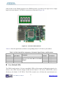
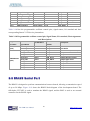
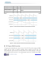
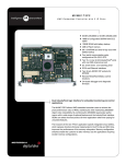
1
TR5-F40W User Manual 1 www.terasic.com August 29, 2014 CONTENTS CHAPTER 1 OVERVIEW .......................................................................................................................................... 4 1.1 GENERAL DESCRIPTION ............................................................................................................................................ 4 1.2 KEY FEATURES.......................................................................................................................................................... 4 1.3 BLOCK DIAGRAM ...................................................................................................................................................... 6 CHAPTER 2 BOARD COMPONENTS .................................................................................................................... 9 2.1 BOARD OVERVIEW .................................................................................................................................................... 9 2.2 CONFIGURATION, STATUS AND SETUP ..................................................................................................................... 10 2.3 GENERAL USER INPUT/OUTPUT .............................................................................................................................. 15 2.4 TEMPERATURE SENSOR AND FAN CONTROL ............................................................................................................ 17 2.5 CLOCK CIRCUIT ...................................................................................................................................................... 18 2.6 RS422 SERIAL PORT ............................................................................................................................................... 20 2.7 FLASH MEMORY ................................................................................................................................................... 21 2.8 SSRAM .................................................................................................................................................................. 24 2.9 SPF+ PORTS ............................................................................................................................................................ 26 2.10 PCI EXPRESS......................................................................................................................................................... 29 2.11 SATA .................................................................................................................................................................... 31 2.12 HSMC: HIGH-SPEED MEZZANINE CARD .............................................................................................................. 34 CHAPTER 3 SYSTEM BUILDER ........................................................................................................................... 42 3.1 INTRODUCTION ....................................................................................................................................................... 42 3.2 GENERAL DESIGN FLOW ......................................................................................................................................... 43 3.3 USING SYSTEM BUILDER ........................................................................................................................................ 44 CHAPTER 4 FLASH PROGRAMMING ................................................................................................................. 51 4.1 CFI FLASH MEMORY MAP ...................................................................................................................................... 51 4.2 FPGA CONFIGURE OPERATION ............................................................................................................................... 52 4.3 FLASH PROGRAMMING WITH USERS DESIGN .......................................................................................................... 52 4.4 RESTORE FACTORY SETTINGS ................................................................................................................................. 54 CHAPTER 5 PROGRAMMABLE OSCILLATOR ................................................................................................. 56 5.1 OVERVIEW .............................................................................................................................................................. 56 5.2 SI570 EXAMPLE (RTL) ........................................................................................................................................... 60 TR5-F40W User Manual 2 www.terasic.com August 29, 2014 5.3 SI570 AND CDCM PROGRAMMING (NIOS II) .......................................................................................................... 68 CHAPTER 6 PCI EXPRESS REFERENCE DESIGN ......................................................................................... 73 6.1 PCI EXPRESS SYSTEM INFRASTRUCTURE ................................................................................................................ 73 6.2 FPGA PCI EXPRESS SYSTEM DESIGN ..................................................................................................................... 74 6.3 PC PCI EXPRESS SYSTEM DESIGN .......................................................................................................................... 78 6.4 FUNDAMENTAL COMMUNICATION ........................................................................................................................... 88 6.5 EXAMPLE 2: IMAGE PROCESS APPLICATION ............................................................................................................ 93 ADDITIONAL INFORMATION ..................................................................................................................................... 98 TR5-F40W User Manual 3 www.terasic.com August 29, 2014 Chapter 1 Overview This chapter provides an overview of the TR5-F40W Development Board and installation guide. 1.1 General Description The Terasic TR5-F40W Stratix V GX FPGA Development Kit provides the ideal hardware platform for developing high-performance and high-bandwidth application. With a standard-height, half-length form-factor package, the TR5-F40W is designed for the most demanding high-end applications, empowered with the top-of-the-line Altera Stratix V GX, delivering the best system-level integration and flexibility in the industry. The Stratix® V GX FPGA features 340K logic elements and integrated transceivers that transfer at a maximum of 12.5 Gbps, allowing the TR5-F40W to be fully compliant with version 3.0 of SATA, version 3.0 of the PCI Express standard, as well as allowing an ultra low-latency, straight connections to four external 10G SFP+ modules. Not relying on an external PHY will accelerate mainstream development of network applications enabling customers to deploy designs for a broad range of high-speed connectivity applications. An HSMC expansion port also allows users to connect custom daughter cards such as those found on cards.terasic.com. The feature-set of the TR5-F40W fully supports all high-intensity applications such as low-latency trading, cloud computing, high-performance computing, data acquisition, network processing, and signal processing. 1.2 Key Features The following hardware is implemented on the TR5-F40W board: FPGA o Altera Stratix® V GX FPGA (5SGXEA3K2F40C3) TR5-F40W User Manual 4 www.terasic.com August 29, 2014 FPGA Configuration o On-Board USB Blaster II or JTAG header for FPGA programming o Fast passive parallel (FPPx32) configuration via MAX II CPLD and flash memory General user input/output: o 10 LEDs o 4 push-buttons o 4 slide switches On-Board Clock o 50MHz Oscillator o Programmable oscillators Si570 and CDCM61004 o SMA connector for external clock input / output Memory o SSRAM o FLASH Communication Ports o Four SFP+ connectors o One SATA host port o One SATA device port o PCI Express (PCIe) x8 edge connector o One RS422 transceiver with RJ45 connector o One HSMC Connector System Monitor and Control o Temperature sensor o Fan control Power o PCI Express 6-pin power connector, 12V DC Input o PCI Express edge connector power Mechanical Specification TR5-F40W User Manual 5 www.terasic.com August 29, 2014 o PCI Express standard-height and half-length 1.3 Block Diagram Figure 1-1 shows the block diagram of the TR5-F40W board. To provide maximum flexibility for the users, all key components are connected with the Stratix V GX FPGA device. Thus, users can configure the FPGA to implement any system design. Figure 1-1 Block diagram of the TR5-F40W board Stratix V GX FPGA 5SGXEA3K2F40C3 340,000 logic elements (LEs) 19-Mbits embedded memory 36 transceivers (12.5Gbps) TR5-F40W User Manual 6 www.terasic.com August 29, 2014 512 18-bit x 18-bit multipliers 256 27-bit x 27-bit DSP blocks 2 PCI Express hard IP blocks 696 user I/Os 174 full-duplex LVDS channels 24 phase locked loops (PLLs) JTAG Header and FPGA Configuration On-board USB Blaster II or JTAG header for use with the Quartus II Programmer MAXII CPLD EPM2210 System Controller and Fast Passive Parallel (FPP) configuration Memory devices 2MB SSRAM 256MB FLASH General user I/O 10 user controllable LEDs 4 user push buttons 4 user slide switches On-Board Clock 50MHz oscillator Programmable oscillators providing clock for 10G SFP+ transceiver Programmable oscillators providing clock for SATA, HSMC and 1G SFP+ transceiver 1 SMA connector for external clock output 1 SMA connector for external clock input HSMC Connector TR5-F40W User Manual 7 www.terasic.com August 29, 2014 Total of 8 pairs transceivers at data rate up to 12.5Gbps Total of 18 LVDS channels (also can be configured as single-end signals) Input and output clock JTAG Signals Adjustable I/O voltage 1.5V / 1.8V / 2.5V Two Serial ATA ports SATA 3.0 standard at 6Gbps signaling rate Four SFP+ ports Four SFP+ connector (10 Gbps+) PCI Express x8 edge connector Support for PCIe Gen1/2/3 Edge connector for PC motherboard with x8 or x16 PCI Express slot Power Source PCI Express 6-pin DC 12V power PCI Express edge connector power TR5-F40W User Manual 8 www.terasic.com August 29, 2014 Chapter 2 Board Components This chapter introduces all the important components on the TR5-F40W. 2.1 Board Over view Figure 2-1 is the top and bottom view of the TR5-F40W development board. It depicts the layout of the board and indicates the location of the connectors and key components. Users can refer to this figure for relative location of the connectors and key components. Figure 2-1 The FPGA Board (Top) 9 Figure 2-2 The FPGA Board (Bottom) 2.2 Configuration, Status and Setup Configure The FPGA board supports two configuration methods for the Stratix V FPGA: Configure the FPGA using the on-board USB-Blaster II. Flash memory configuration of the FPGA using stored images from the flash memory on power-up. For programming via on-board USB-Blaster II, the following procedures show how to download a configuration bit stream into the Stratix V GX FPGA: Make sure that power is provided to the FPGA board Connect your PC to the FPGA board using a mini-USB cable and make sure the USB-Blaster II driver is installed on your PC. Launch Quartus II programmer and make sure the USB-Blaster II is detected. In Quartus II Programmer, add the configuration bit stream file (.sof), check the associated TR5-F40W User Manual 10 www.terasic.com August 29, 2014 “Program/Configure” item, and click “Start” to start FPGA programming. Status LED The FPGA Board development board includes board-specific status LEDs to indicate board status. Please refer to Table 2-1 for the description of the LED indicator. Table 2-1 Status LED Board Reference LED Name Description D7 12-V Power Illuminates when 12-V power is active. D6 3.3-V Power Illuminates when 3.3-V power is active. D25 HSMC Power 1.5-V : no Illuminates 1.8-V : Illuminates Green 2.5-V : Illuminates Red (Default) D19 CONF DONE Illuminates when the FPGA is successfully configured. Driven by the MAX II CPLD EPM2210 System Controller. D15 Loading Illuminates when the MAX II CPLD EPM2210 System Controller is actively configuring the FPGA. Driven by the MAX II CPLD EPM2210 System Controller with the Embedded Blaster CPLD. D17 Error Illuminates when the MAX II CPLD EPM2210 System Controller fails to configure the FPGA. Driven by the MAX II CPLD EPM2210 System Controller. D18 PAGE Illuminates when FPGA is configured by the factory configuration bit stream. Setup HSMC I/O voltage The FPGA I/O standards of the HSMC ports can be adjusted by configuring the header position (J3). Each port can be individually adjusted to 1.5V, 1.8V, 2.5V via jumpers on the top-right. Figure 2-3 depicts the position of the jumpers and their associated I/O standards. Users can use 2-pin jumpers to configure the I/O standard by choosing the associated positions on the header. Please refer to Table 2-2 for more details. Note: removing or mounting all of the jumpers will force an output of 1.5V, and will incur the risk of damaging your FPGA. TR5-F40W User Manual 11 www.terasic.com August 29, 2014 Figure 2-3 HSMC I/O Configuration Header Table 2-2 HSMC IO Standard Select Board Reference Signal Name Description Default J3.1 – J3.2 HSMC VCCIO 1.5V Short : Select VCCIO = 1.5V output Open J3.3 – J3.4 HSMC VCCIO 1.8V Short : Select VCCIO = 1.8V output Open J3.5 – J3.6 HSMC VCCIO 2.5V Short : Select VCCIO = 2.5V output Short J3.7 – J3.8 HSMC VCCIO 1.5V Short : Select VCCIO = 1.5V output Open Setup PCI Express Control DIP switch The PCI Express Control DIP switch (SW8) is provided to enable or disable different configurations of the PCIe Connector. Table 2-3 lists the switch controls and description. Table 2-3 SW8 PCIe Control DIP Switch Board Reference Signal Name Description Default SW8.1 PCIE_PRSNT2n_x1 On : Enable x1 presence detect Off : Disable x1 presence detect Off SW8.2 PCIE_PRSNT2n_x4 On : Enable x4 presence detect Off : Disable x4 presence detect Off SW8.3 PCIE_PRSNT2n_x8 On : Enable x8 presence detect Off : Disable x8 presence detect On TR5-F40W User Manual 12 www.terasic.com August 29, 2014 Setup Configure Mode Control DIP switch The Configure Mode Control DIP switch (SW7) is provided to specify the configuration mode of the FPGA. Because currently only one mode is supported, please set all positions as shown in Figure 2-4. Figure 2-4 6-Position DIP switch for Configure Mode Select Flash Image for Configuration The Image Select DIP switch (SW5) is provided to specify the image for configuration of the FPGA. Setting SW5 to the top specifies the default factory image to be loaded, as shown in Figure 2-5. Setting SW5 to low specifies the TR5-F40W to load a user-defined image, as shown in Figure 2-6. Figure 2-5 DIP switch for Image Select – Factory Image Load TR5-F40W User Manual 13 www.terasic.com August 29, 2014 Figure 2-6 DIP switch for Image Select – User Image Load Select JTAG Chain DIP Switch Table 2-4 explains the configuration for SW6. SW6.1 enables/disables the USB Blaster. SW6.3 selects the JTAG chain. A more detailed explanation can be found in Chapter 2-12 JTAG Chain on HSMC. Table 2-4 SW6 JTAG Chain DIP Switch Board Reference Signal Name Description Default SW6.1 On-Board USB Blaster On : Disable On-Board USB Blaster Off Off : Enable On-Board USB Blaster SW6.2 N/A N/A On SW6.3 HSMC JTAG On : Disable HSMC JTAG chain Off : Enable HSMC JTAG chain On SW6.4 N/A N/A On TR5-F40W User Manual 14 www.terasic.com August 29, 2014 Figure 2-7 SW6 4-Position JTAG Chain DIP Switch Settings 2.3 General User Input/Output This section describes the user I/O interface to the FPGA. User Defined Push-buttons The FPGA board includes four user defined push-buttons that allow users to interact with the Stratix V GX device. Each push-button provides a high logic level or a low logic level when it is not pressed or pressed, respectively. Table 2-5 lists the board references, signal names and their corresponding Stratix V GX device pin numbers. Table 2-5 Push-button Pin Assignments, Schematic Signal Names, and Functions Board Schematic Reference Signal Name PB0 BUTTON0 PB1 BUTTON1 PB2 BUTTON2 PB3 BUTTON3 Description High Logic Level when the button is not pressed I/O Stratix V GX Standard Pin Number 2.5-V PIN_C18 2.5-V PIN_B19 2.5-V PIN_B17 2.5-V PIN_A17 User-Defined Slide Switch There are four slide switches on the FPGA board to provide additional FPGA input control. When a TR5-F40W User Manual 15 www.terasic.com August 29, 2014 slide switch is in the DOWN position or the UPPER position, it provides a low logic level or a high logic level to the Stratix V GX FPGA, respectively, as shown in Figure 2-8. Figure 2-8 4-Position Slide switches Table 2-6 lists the signal names and their corresponding Stratix V GX device pin numbers. Table 2-6 Slide Switch Pin Assignments, Schematic Signal Names, and Functions Board Schematic Reference Signal Name Description I/O Stratix V GX Standard Pin Number SW0 SW0 2.5-V PIN_F17 SW1 SW1 PIN_G17 SW2 SW2 High logic level when SW in the UPPER 2.5-V position. 2.5-V SW3 SW3 2.5-V PIN_G16 PIN_G19 User-Defined LEDs The FPGA board consists of 10 user-controllable LEDs to allow status and debugging signals to be driven to the LEDs from the designs loaded into the Stratix V GX device. Each LED is driven directly by the Stratix V GX FPGA. The LED is turned on or off when the associated pins are TR5-F40W User Manual 16 www.terasic.com August 29, 2014 driven to a low or high logic level, respectively. A list of the pin names on the FPGA that are connected to the LEDs is given in Table 2-7. Table 2-7 User LEDs Pin Assignments, Schematic Signal Names, and Functions Board Schematic Reference Signal Name I/O Description Stratix V GX Standard Pin Number D0 LED0 2.5-V PIN_C16 D1 LED1 2.5-V PIN_D18 D2 LED2 2.5-V PIN_B16 D3 LED3 PIN_A16 D5-1 LED_BRACKET0 D5-3 LED_BRACKET1 D5-5 LED_BRACKET2 Driving a logic low on the I/O port turns the 2.5-V 2.5-V LED ON. Driving a logic high on the I/O port turns 2.5-V the LED OFF. 2.5-V D5-7 LED_BRACKET3 2.5-V PIN_D16 J6-10 LED_RJ45_L 2.5-V PIN_M15 J6-12 LED_RJ45_R 2.5-V PIN_N15 PIN_E18 PIN_E17 PIN_E19 2.4 Temperature Sensor and Fan Control The FPGA board is equipped with a temperature sensor, MAX1619, which provides temperature sensing and over-temperature alert. These functions are accomplished by connecting the temperature sensor to the internal temperature sensing diode of the Stratix V GX device. The temperature status and alarm threshold registers of the temperature sensor can be programmed by a two-wire SMBus, which is connected to the Stratix V GX FPGA. In addition, the 7-bit POR slave address for this sensor is set to ‘0011000b’. An optional 3-pin +12V fan located on J15 of the FPGA board is intended to reduce the temperature of the FPGA. Users can control the fan to turn on/off depending on the measured system temperature. The FAN is turned on when the FAN_CTRL pin is driven to a high logic level or tri-state. The pin assignments for the associated interface are listed in Table 2-8. Table 2-8 Temperature Sensor Pin Assignments, Schematic Signal Names, and Functions Schematic Signal Name TEMPDIODEp Description I/O Standard Positive pin of temperature diode in Stratix V TR5-F40W User Manual 17 2.5-V Stratix V GX Pin Number PIN_R6 www.terasic.com August 29, 2014 TEMPDIODEn Negative pin of temperature diode in Stratix V 2.5-V PIN_P5 TEMP_CLK SMBus clock 2.5-V PIN_AM17 TEMP_DATAT SMBus data 2.5-V PIN_AN17 TEMP_OVERT_n SMBus alert (interrupt) 2.5-V PIN_AR17 TEMP_INT_n SMBus alert (interrupt) 2.5-V PIN_AT17 FAN_CTRL Fan control 2.5-V PIN_AW16 2.5 Clock Circuit The development board includes one 50 MHz and two programmable oscillators. Figure 2-9 shows the default frequencies of on-board all external clocks going to the Stratix V GX FPGA. The figures also show an off-board external clock from PCI Express Host to the FPGA. Lastly, there is an SMA connector for clock input, and an SMA connector for clock output. Figure 2-9 Clock Circuit of the FPGA Board A clock buffer is used to duplicate the 50 MHz oscillator, so each bank of FPGA I/O bank 3/4/7/8 has two clock inputs. The two programming oscillators are low-jitter oscillators which are used to provide special and high quality clock signals for high-speed transceivers. Figure 2-10 shows the TR5-F40W User Manual 18 www.terasic.com August 29, 2014 control circuits of programmable oscillators. The CDCM61004 oscillator can be programmed to generate a desired reference clock for the 1G Ethernet SFP+ transceiver, SATA Host/Device transceiver and eight transceivers in the HSMC connector. The Si570 programmable oscillator is programmed via an I2C serial interface to generate the reference clock for 10G Ethernet SFP+ transceiver. Figure 2-10 Control Circuits of Programmable Oscillators Table 2-9 lists the clock source, signal names, default frequency and their corresponding Stratix V GX device pin numbers. Table 2-9 Clock Source, Signal Name, Default Frequency, Pin Assignments and Functions Source Y3 Schematic Default Signal Name Frequency I/O Standard Stratix V GX Pin Number OSC_50_B3B 2.5-V PIN_AV29 OSC_50_B3D 2.5-V PIN_AK23 OSC_50_B4A 2.5-V PIN_AL7 OSC_50_B4D 2.5-V PIN_AF17 2.5-V PIN_G7 OSC_50_B7D 2.5-V PIN_P16 OSC_50_B8A 1.5-V/1.8-V/2.5-V PIN_E34 OSC_50_B8D 1.5-V/1.8-V/2.5-V PIN_J23 OSC_50_B7A 50.0 MHz TR5-F40W User Manual 19 Application www.terasic.com August 29, 2014 U10 SFP_REFCLK_p 100.0 MHz HCSL PIN_AF6 10G SFP+ U27 SFP1G_REFCLK_p 125.0 MHz HCSL PIN_AB6 1G SFP+ U27 SATA_REFCLK_p 125.0 MHz HCSL PIN_V6 SATA U27 HSMC_REFCLK_p 125.0 MHz HCSL PIN_V34 HSMC XCVR J15 PCIE_REFCLK_p From Host HCSL PIN_AF34 PCI Express J12 SMA_CLKIN User input 2.5-V PIN_U15 J14 SMA_CLKOUT User output 2.5-V PIN_AD30 Table 2-10 lists the programmable oscillator control pins, signal names, I/O standard and their corresponding Stratix V GX device pin numbers. Table 2-10 Programmable oscillator control pin, Signal Name, I/O standard, Pin Assignments and Descriptions Programmable Schematic Oscillator Si570 (U10) CDCM61004 (U27) Signal Name I/O Standard Stratix V GX Pin Number Description CLOCK_SCL 2.5-V PIN_AD15 CLOCK_SDA 2.5-V PIN_AD16 I2C bus, direct connected with Si570 CLK_RST_n 2.5-V PIN_AC15 Device reset (active low) CLK_CE 2.5-V PIN_AH15 Chip enable CLK_PR0 2.5-V PIN_AB16 Output divider control CLK_PR1 2.5-V PIN_AJ15 Output divider control CLK_OS0 2.5-V PIN_AG14 Output type select CLK_OS1 2.5-V PIN_AG15 Output type select CLK_OD0 2.5-V PIN_AB15 Output divider control CLK_OD1 2.5-V PIN_AA15 Output divider control CLK_OD2 2.5-V PIN_AA14 Output divider control 2.6 RS422 Serial Por t The RS422 is designed to perform communication between boards, allowing a transmission speed of up to 20 Mbps. Figure 2-11 shows the RS422 block diagram of the development board. The full-duplex LTC2855 is used to translate the RS422 signal, and the RJ45 is used as an external connector for the RS422 signal. TR5-F40W User Manual 20 www.terasic.com August 29, 2014 Figure 2-11 Block Diagram of RS422 Table 2-11 lists the RS422 pin assignments, signal names and functions. Table 2-11 RS422 Pin Assignments, Schematic Signal Names, and Functions Schematic Description Signal Name I/O Standard Stratix V GX Pin Number RS422_DE Driver Enable. A high on DE enables the driver. A low input will force the driver outputs into a high impedance state. PIN_K16 RS422_DIN Receiver Output. The data is send to FPGA. PIN_H19 RS422_DOUT Driver Input. The data is sent from FPGA. PIN_H17 RS422_RE_n Receiver Enable. A low enables the receiver. A 2.5-V high input forces the receiver output into a high impedance state. PIN_L16 Internal Termination Resistance Enable. A high RS422_TE input will connect a termination resistor (120Ω PIN_H16 typical) between pins A and B. 2.7 FLASH Memor y The development board has two 1Gb CFI-compatible synchronous flash devices for non-volatile storage of FPGA configuration data, user application data, and user code space. Each interface has a 16-bit data bus and the two devices combined allow for FPP x32 configuration. This device is part of the shared flash, SSRAM and MAX (FSM) bus, which connects to the flash TR5-F40W User Manual 21 www.terasic.com August 29, 2014 memory, SSRAM memory and MAX II CPLD (EPM2210) System Controller. Figure 2-12 shows the connections between the Flash, SSRAM, MAX II CPLD and Stratix V GX FPGA. Figure 2-12 Connection between the Flash, Max and Stratix V GX FPGA Table 2-12 lists the flash pin assignments, signal names, and functions. Table 2-12 Flash Memory Pin Assignments, Schematic Signal Names, and Functions Schematic Signal Name Description I/O Standard Stratix V GX Pin Number FSM_A0 Address bus 2.5-V PIN_AW22 FSM_A1 Address bus 2.5-V PIN_AV23 FSM_A2 Address bus 2.5-V PIN_AV25 FSM_A3 Address bus 2.5-V PIN_AT24 FSM_A4 Address bus 2.5-V PIN_AN23 FSM_A5 Address bus 2.5-V PIN_AW23 FSM_A6 Address bus 2.5-V PIN_AU23 FSM_A7 Address bus 2.5-V PIN_AP24 FSM_A8 Address bus 2.5-V PIN_AM25 FSM_A9 Address bus 2.5-V PIN_AM26 FSM_A10 Address bus 2.5-V PIN_AP25 FSM_A11 Address bus 2.5-V PIN_AP22 FSM_A12 Address bus 2.5-V PIN_AL24 FSM_A13 Address bus 2.5-V PIN_AM23 TR5-F40W User Manual 22 www.terasic.com August 29, 2014 FSM_A14 Address bus 2.5-V PIN_AH24 FSM_A15 Address bus 2.5-V PIN_AG25 FSM_A16 Address bus 2.5-V PIN_AK24 FSM_A17 Address bus 2.5-V PIN_AM22 FSM_A18 Address bus 2.5-V PIN_AL25 FSM_A19 Address bus 2.5-V PIN_AT23 FSM_A20 Address bus 2.5-V PIN_AJ26 FSM_A21 Address bus 2.5-V PIN_AT26 FSM_A22 Address bus 2.5-V PIN_AR22 FSM_A23 Address bus 2.5-V PIN_AU24 FSM_A24 Address bus 2.5-V PIN_AR24 FSM_A25 Address bus 2.5-V PIN_AN22 FSM_A26 Address bus 2.5-V PIN_AR25 FSM_D0 Data bus 2.5-V PIN_AJ24 FSM_D1 Data bus 2.5-V PIN_AH27 FSM_D2 Data bus 2.5-V PIN_AG27 FSM_D3 Data bus 2.5-V PIN_AG26 FSM_D4 Data bus 2.5-V PIN_AG24 FSM_D5 Data bus 2.5-V PIN_AG23 FSM_D6 Data bus 2.5-V PIN_AC27 FSM_D7 Data bus 2.5-V PIN_AC26 FSM_D8 Data bus 2.5-V PIN_AA26 FSM_D9 Data bus 2.5-V PIN_AF23 FSM_D10 Data bus 2.5-V PIN_AG22 FSM_D11 Data bus 2.5-V PIN_AF22 FSM_D12 Data bus 2.5-V PIN_AD21 FSM_D13 Data bus 2.5-V PIN_AE21 FSM_D14 Data bus 2.5-V PIN_AE20 FSM_D15 Data bus 2.5-V PIN_AD20 FSM_D16 Data bus 2.5-V PIN_AE22 FSM_D17 Data bus 2.5-V PIN_AD22 FSM_D18 Data bus 2.5-V PIN_AB24 FSM_D19 Data bus 2.5-V PIN_AD24 FSM_D20 Data bus 2.5-V PIN_AC24 FSM_D21 Data bus 2.5-V PIN_AA25 FSM_D22 Data bus 2.5-V PIN_AB25 FSM_D23 Data bus 2.5-V PIN_AC25 FSM_D24 Data bus 2.5-V PIN_AE25 FSM_D25 Data bus 2.5-V PIN_AD26 FSM_D26 Data bus 2.5-V PIN_AE26 FSM_D27 Data bus 2.5-V PIN_AE24 FSM_D28 Data bus 2.5-V PIN_AF25 FSM_D29 Data bus 2.5-V PIN_AF26 TR5-F40W User Manual 23 www.terasic.com August 29, 2014 FSM_D30 Data bus 2.5-V PIN_AA27 FSM_D31 Data bus 2.5-V PIN_AB27 FLASH_CLK Clock 2.5-V PIN_AB30 FLASH_RESET_n Reset 2.5-V PIN_AT27 FLASH_CE_n[0] Chip enable of of flash-0 2.5-V PIN_AU25 FLASH_CE_n[1] Chip enable of of flash-1 2.5-V PIN_AN24 FLASH_OE_n Output enable 2.5-V PIN_AP27 FLASH_WE_n Write enable 2.5-V PIN_AP28 FLASH_ADV_n Address valid 2.5-V PIN_AR27 FLASH_RDY_BSY_n[0] Ready of flash-0 2.5-V PIN_AU26 FLASH_RDY_BSY_n[1] Ready of flash-1 2.5-V PIN_AR28 2.8 SSRAM The IS61LPS51236A Synchronous Static Random Access Memory (SSRAM) device featured on the TR5-F40W development board is part of the shared FMS Bus, which connects to flash memory, SSRAM, and the MAX II CPLD (EEPM2210) System Controller. Table 2-13 lists the SSRAM pin assignments, signal names relative to the Stratix V GX device, in respectively. Table 2-13 SSRAM Pin Assignments, Schematic Signal Names, and Functions Schematic Signal Name Description I/O Standard Stratix V GX Pin Number FSM_A0 Address bus 2.5-V PIN_AW22 FSM_A1 Address bus 2.5-V PIN_AV23 FSM_A2 Address bus 2.5-V PIN_AV25 FSM_A3 Address bus 2.5-V PIN_AT24 FSM_A4 Address bus 2.5-V PIN_AN23 FSM_A5 Address bus 2.5-V PIN_AW23 FSM_A6 Address bus 2.5-V PIN_AU23 FSM_A7 Address bus 2.5-V PIN_AP24 FSM_A8 Address bus 2.5-V PIN_AM25 FSM_A9 Address bus 2.5-V PIN_AM26 FSM_A10 Address bus 2.5-V PIN_AP25 FSM_A11 Address bus 2.5-V PIN_AP22 FSM_A12 Address bus 2.5-V PIN_AL24 FSM_A13 Address bus 2.5-V PIN_AM23 FSM_A14 Address bus 2.5-V PIN_AH24 FSM_A15 Address bus 2.5-V PIN_AG25 TR5-F40W User Manual 24 www.terasic.com August 29, 2014 FSM_A16 Address bus 2.5-V PIN_AK24 FSM_A17 Address bus 2.5-V PIN_AM22 FSM_A18 Address bus 2.5-V PIN_AL25 FSM_A19 Address bus 2.5-V PIN_AT23 FSM_A20 Address bus 2.5-V PIN_AJ26 FSM_A21 Address bus 2.5-V PIN_AT26 FSM_A22 Address bus 2.5-V PIN_AR22 FSM_A23 Address bus 2.5-V PIN_AU24 FSM_A24 Address bus 2.5-V PIN_AR24 FSM_A25 Address bus 2.5-V PIN_AN22 FSM_A26 Address bus 2.5-V PIN_AR25 FSM_D0 Data bus 2.5-V PIN_AJ24 FSM_D1 Data bus 2.5-V PIN_AH27 FSM_D2 Data bus 2.5-V PIN_AG27 FSM_D3 Data bus 2.5-V PIN_AG26 FSM_D4 Data bus 2.5-V PIN_AG24 FSM_D5 Data bus 2.5-V PIN_AG23 FSM_D6 Data bus 2.5-V PIN_AC27 FSM_D7 Data bus 2.5-V PIN_AC26 FSM_D8 Data bus 2.5-V PIN_AA26 FSM_D9 Data bus 2.5-V PIN_AF23 FSM_D10 Data bus 2.5-V PIN_AG22 FSM_D11 Data bus 2.5-V PIN_AF22 FSM_D12 Data bus 2.5-V PIN_AD21 FSM_D13 Data bus 2.5-V PIN_AE21 FSM_D14 Data bus 2.5-V PIN_AE20 FSM_D15 Data bus 2.5-V PIN_AD20 FSM_D16 Data bus 2.5-V PIN_AE22 FSM_D17 Data bus 2.5-V PIN_AD22 FSM_D18 Data bus 2.5-V PIN_AB24 FSM_D19 Data bus 2.5-V PIN_AD24 FSM_D20 Data bus 2.5-V PIN_AC24 FSM_D21 Data bus 2.5-V PIN_AA25 FSM_D22 Data bus 2.5-V PIN_AB25 FSM_D23 Data bus 2.5-V PIN_AC25 FSM_D24 Data bus 2.5-V PIN_AE25 FSM_D25 Data bus 2.5-V PIN_AD26 FSM_D26 Data bus 2.5-V PIN_AE26 FSM_D27 Data bus 2.5-V PIN_AE24 FSM_D28 Data bus 2.5-V PIN_AF25 FSM_D29 Data bus 2.5-V PIN_AF26 FSM_D30 Data bus 2.5-V PIN_AA27 FSM_D31 Data bus 2.5-V PIN_AB27 TR5-F40W User Manual 25 www.terasic.com August 29, 2014 SSRAM_DPA0 Data bus 2.5-V PIN_AK30 SSRAM_DPA1 Data bus 2.5-V PIN_AN25 SSRAM_DPA2 Data bus 2.5-V PIN_AL27 SSRAM_DPA3 Data bus 2.5-V PIN_AN27 SSRAM_CLK Synchronous Clock 2.5-V PIN_AE30 SSRAM_BE_n0 Synchronous Byte lane 0 Write Input 2.5-V PIN_AJ29 SSRAM_BE_n1 Synchronous Byte lane 1 Write Input 2.5-V PIN_AL28 SSRAM_BE_n2 Synchronous Byte lane 2 Write Input 2.5-V PIN_AK27 SSRAM_BE_n3 Synchronous Byte lane 3 Write Input 2.5-V PIN_AH25 SSRAM_OE_n Output Enable 2.5-V PIN_AM28 SSRAM_CE1_n Synchronous Chip enable 2.5-V PIN_AL26 SSRAM_WE_n Write enable 2.5-V PIN_AK29 SSRAM_GW_n Synchronous Burst Address Advance 2.5-V PIN_AL30 SSRAM_ADV_n Address Status Controller 2.5-V PIN_AN26 SSRAM_ADSC_n Address Status Controller 2.5-V PIN_AM29 SSRAM_ADSP_n Address Status Processor 2.5-V PIN_AN28 SSRAM_MODE Burst Sequence Selection 2.5-V PIN_AJ27 SSRAM_ZZ Power Sleep Mode 2.5-V PIN_AL29 2.9 SPF+ Por ts The development board has four independent 10G SFP+ connectors that use one transceiver channel each from the Stratix V GX FPGA device. These modules take in serial data from the Stratix V GX FPGA device and transform them to optical signals. The board includes cage assemblies for the SFP+ connectors. Figure 2-13 shows the connections between the SFP+ and Stratix V GX FPGA. TR5-F40W User Manual 26 www.terasic.com August 29, 2014 Figure 2-13 Connection between the SFP+ and Stratix V GX FPGA Table 2-14 to Table 2-17 list the SFP+ A, B, C and D pin assignments and signal names relative to the Stratix V GX device. Table 2-14 SFP+ A Pin Assignments, Schematic Signal Names, and Functions Schematic Signal Name Description I/O Standard Stratix V GX Pin Number SFPA_TX_p Transmitter data 1.4-V PCML PIN_AA4 SFPA_TX_n Transmitter data 1.4-V PCML PIN_AA3 SFPA_RX_p Receiver data 1.4-V PCML PIN_AB2 SFPA_RX_n Receiver data 1.4-V PCML PIN_AB1 SFPA_LOS Signal loss indicator 2.5V PIN_AE10 SFPA_MOD0_PRSNT_n Module present 2.5V PIN_AD9 SFPA_MOD1_SCL Serial 2-wire clock 2.5V PIN_AC9 SFPA_MOD2_SDA Serial 2-wire data 2.5V PIN_AC12 SFPA_RATESEL0 Rate select 0 2.5V PIN_AE11 SFPA_RATESEL1 Rate select 1 2.5V PIN_AE9 SFPA_TXDISABLE Turns off and disables the transmitter output 2.5V PIN_AB9 SFPA_TXFAULT Transmitter fault 2.5V PIN_AB12 Table 2-15 SFP+ B Pin Assignments, Schematic Signal Names, and Functions Schematic Signal Name Description TR5-F40W User Manual I/O Standard 27 Stratix V GX Pin Number www.terasic.com August 29, 2014 SFPB_TX_p Transmitter data 1.4-V PCML PIN_AE4 SFPB_TX_n Transmitter data 1.4-V PCML PIN_AE3 SFPB_RX_p Receiver data 1.4-V PCML PIN_AF2 SFPB_RX_n Receiver data 1.4-V PCML PIN_AF1 SFPB_LOS Signal loss indicator 2.5V PIN_AN9 SFPB_MOD0_PRSNT_n Module present 2.5V PIN_AM10 SFPB_MOD1_SCL Serial 2-wire clock 2.5V PIN_AM11 SFPB_MOD2_SDA Serial 2-wire data 2.5V PIN_AL10 SFPB_RATESEL0 Rate select 0 2.5V PIN_AN11 SFPB_RATESEL1 Rate select 1 2.5V PIN_AP9 SFPB_TXDISABLE Turns off and disables the transmitter output 2.5V PIN_AL11 SFPB_TXFAULT Transmitter fault 2.5V PIN_AK11 Table 2-16 SFP+ C Pin Assignments, Schematic Signal Names, and Functions Schematic Description Signal Name I/O Standard Stratix V GX Pin Number SFPC_TX_p Transmitter data 1.4-V PCML PIN_AN4 SFPC_TX_n Transmitter data 1.4-V PCML PIN_AN3 SFPC_RX_p Receiver data 1.4-V PCML PIN_AP2 SFPC_RX_n Receiver data 1.4-V PCML PIN_AP1 SFPC_LOS Signal loss indicator 2.5V PIN_AK12 SFPC_MOD0_PRSNT_n Module present 2.5V PIN_AH9 SFPC_MOD1_SCL Serial 2-wire clock 2.5V PIN_AH10 SFPC_MOD2_SDA Serial 2-wire data 2.5V PIN_AG9 SFPC_RATESEL0 Rate select 0 2.5V PIN_AJ10 SFPC_RATESEL1 Rate select 1 2.5V PIN_AL12 SFPC_TXDISABLE Turns off and disables the transmitter output 2.5V PIN_AG12 SFPC_TXFAULT Transmitter fault 2.5V PIN_AF11 Table 2-17 SFP+ D Pin Assignments, Schematic Signal Names, and Functions Schematic Description Signal Name I/O Standard Stratix V GX Pin Number SFPD_TX_p Transmitter data 1.4-V PCML PIN_AU4 SFPD_TX_n Transmitter data 1.4-V PCML PIN_AU3 SFPD_RX_p Receiver data 1.4-V PCML PIN_AV2 SFPD_RX_n Receiver data 1.4-V PCML PIN_AV1 SFPD_LOS Signal loss indicator 2.5V PIN_AV11 SFPD_MOD0_PRSNT_n Module present 2.5V PIN_AU10 SFPD_MOD1_SCL Serial 2-wire clock 2.5V PIN_AU9 SFPD_MOD2_SDA Serial 2-wire data 2.5V PIN_AT9 TR5-F40W User Manual 28 www.terasic.com August 29, 2014 SFPD_RATESEL0 Rate select 0 2.5V PIN_AU11 SFPD_RATESEL1 Rate select 1 2.5V PIN_AW11 SFPD_TXDISABLE Turns off and disables the transmitter output 2.5V PIN_AT11 SFPD_TXFAULT Transmitter fault 2.5V PIN_AR9 2.10 PCI Express The FPGA development board is designed to fit entirely into a PC motherboard with x8 or x16 PCI Express slot. Utilizing built-in transceivers on a Stratix V GX device, it is able to provide a fully integrated PCI Express-compliant solution for multi-lane (x1, x4, and x8) applications. With the PCI Express hard IP block incorporated in the Stratix V GX device, it will allow users to implement simple and fast protocol, as well as saving logic resources for logic application. Figure 2-14 presents the pin connection established between the Stratix V GX and PCI Express. The PCI Express interface supports complete PCI Express Gen1 at 2.5Gbps/lane, Gen2 at 5.0Gbps/lane, and Gen3 at 8.0Gbps/lane protocol stack solution compliant to PCI Express base specification 3.0 that includes PHY-MAC, Data Link, and transaction layer circuitry embedded in PCI Express hard IP blocks. The power of the board can be sourced entirely from the PCI Express edge connector when installed into a PC motherboard. It is strongly recommended that users connect the PCIe external power connector to 6-pin 12V DC power connector in the FPGA to avoid FPGA damage due to insufficient power. The PCIE_REFCLK_p signal is a differential input that is driven from the PC motherboard on this board through the PCIe edge connector. A DIP switch (SW8) is connected to the PCI Express to allow different configurations to enable a x1, x4, or x8 PCIe. Table 2-18 summarizes the PCI Express pin assignments of the signal names relative to the Stratix V GX FPGA. TR5-F40W User Manual 29 www.terasic.com August 29, 2014 Figure 2-14 PCI Express pin connection Table 2-18 PCI Express Pin Assignments, Schematic Signal Names, and Functions Schematic Signal Name Description I/O Standard Stratix V GX Pin Number PCIE_TX_p0 Add-in card transmit bus 1.4-V PCML PIN_AU36 PCIE_TX_n0 Add-in card transmit bus 1.4-V PCML PIN_AU37 PCIE_TX_p1 Add-in card transmit bus 1.4-V PCML PIN_AR36 PCIE_TX_n1 Add-in card transmit bus 1.4-V PCML PIN_AR37 PCIE_TX_p2 Add-in card transmit bus 1.4-V PCML PIN_AN36 PCIE_TX_n2 Add-in card transmit bus 1.4-V PCML PIN_AN37 PCIE_TX_p3 Add-in card transmit bus 1.4-V PCML PIN_AL36 PCIE_TX_n3 Add-in card transmit bus 1.4-V PCML PIN_AL37 PCIE_TX_p4 Add-in card transmit bus 1.4-V PCML PIN_AG36 PCIE_TX_n4 Add-in card transmit bus 1.4-V PCML PIN_AG37 PCIE_TX_p5 Add-in card transmit bus 1.4-V PCML PIN_AE36 PCIE_TX_n5 Add-in card transmit bus 1.4-V PCML PIN_AE37 PCIE_TX_p6 Add-in card transmit bus 1.4-V PCML PIN_AC36 PCIE_TX_n6 Add-in card transmit bus 1.4-V PCML PIN_AC37 PCIE_TX_p7 Add-in card transmit bus 1.4-V PCML PIN_AA36 PCIE_TX_n7 Add-in card transmit bus 1.4-V PCML PIN_AA37 PCIE_RX_p0 Add-in card receive bus 1.4-V PCML PIN_AV38 PCIE_RX_n0 Add-in card receive bus 1.4-V PCML PIN_AV39 PCIE_RX_p1 Add-in card receive bus 1.4-V PCML PIN_AT38 PCIE_RX_n1 Add-in card receive bus 1.4-V PCML PIN_AT39 PCIE_RX_p2 Add-in card receive bus 1.4-V PCML PIN_AP38 PCIE_RX_n2 Add-in card receive bus 1.4-V PCML PIN_AP39 PCIE_RX_p3 Add-in card receive bus 1.4-V PCML PIN_AM38 TR5-F40W User Manual 30 www.terasic.com August 29, 2014 PCIE_RX_n3 Add-in card receive bus 1.4-V PCML PIN_AM39 PCIE_RX_p4 Add-in card receive bus 1.4-V PCML PIN_AH38 PCIE_RX_n4 Add-in card receive bus 1.4-V PCML PIN_AH39 PCIE_RX_p5 Add-in card receive bus 1.4-V PCML PIN_AF38 PCIE_RX_n5 Add-in card receive bus 1.4-V PCML PIN_AF39 PCIE_RX_p6 Add-in card receive bus 1.4-V PCML PIN_AD38 PCIE_RX_n6 Add-in card receive bus 1.4-V PCML PIN_AD39 PCIE_RX_p7 Add-in card receive bus 1.4-V PCML PIN_AB38 PCIE_RX_n7 Add-in card receive bus 1.4-V PCML PIN_AB39 PCIE_REFCLK_p Motherboard reference clock HCSL PIN_AF34 PCIE_REFCLK_n Motherboard reference clock HCSL PIN_AF35 PCIE_PERST_n Reset 2.5-V PIN_AC28 PCIE_SMBCLK SMB clock 2.5-V PIN_AF28 PCIE_SMBDAT SMB data 2.5-V PIN_AB28 PCIE_WAKE_n Wake signal 2.5-V PIN_AE29 PCIE_PRSNT1n Hot plug detect - - PCIE_PRSNT2n_x1 Hot plug detect x1 PCIe slot enabled using SW8 dip switch - - PCIE_PRSNT2n_x4 Hot plug detect x4 PCIe slot enabled using SW8 dip switch - - PCIE_PRSNT2n_x8 Hot plug detect x8 PCIe slot enabled using SW8 dip switch - - 2.11 SATA Two Serial ATA (SATA) ports are available on the FPGA development board which are computer bus standard with a primary function of transferring data between the motherboard and mass storage devices (such as hard drives, optical drives, and solid-state disks). Supporting a storage interface is just one of many different applications an FPGA can be used in storage appliances. The Stratix V GX device can bridge different protocols such as bridging simple bus I/Os like PCI Express (PCIe) to SATA or network interfaces such as Gigabit Ethernet (GbE) to SATA. The SATA interface supports SATA 3.0 standard with connection speed of 6 Gbps based on Stratix V GX device with integrated transceivers compliant to SATA electrical standards. The two Serial ATA (SATA) ports include one port for device and one port for host capable of implementing SATA solution with a design that consists of both host and target (device side) functions. Figure 2-15 depicts the host and device design examples. TR5-F40W User Manual 31 www.terasic.com August 29, 2014 Figure 2-15 PC and Storage Device Connection to the Stratix V GX FPGA The transmitter and receiver signals of the SATA ports are connected directly to the Stratix V GX transceiver channels to provide SATA IO connectivity to both host and target devices. To verify the functionality of the SATA host/device ports, a connection can be established between the two ports by using a SATA cable as Figure 2-16 depicts the associated signals connected. Table 2-19 lists the SATA pin assignments, signal names and functions. TR5-F40W User Manual 32 www.terasic.com August 29, 2014 Figure 2-16 4 Pin connection between SATA connectors Table 2-19 Serial ATA Pin Assignments, Schematic Signal Names, and Functions Schematic Signal Name Description I/O Standard Stratix V GX Pin Number SATA_REFCLK_p Reference Clock HCSL PIN_V6 SATA_REFCLK_n Reference Clock HCSL PIN_V5 SATA_DEVICE_RX_p0 Differential receive data input after DC blocking capacitor 1.4-V PCML PIN_P2 SATA_DEVICE_RX_n0 Differential receive data input after DC blocking capacitor 1.4-V PCML PIN_P1 SATA_DEVICE_TX_n0 Differential transmit data output before DC blocking capacitor 1.4-V PCML PIN_N4 SATA_DEVICE_TX_p0 Differential transmit data output before DC blocking capacitor 1.4-V PCML PIN_N3 SATA_HOST_TX_p0 Differential transmit data output before DC blocking capacitor 1.4-V PCML PIN_K2 SATA_HOST_TX_n0 Differential transmit data output before DC blocking capacitor 1.4-V PCML PIN_K1 SATA_HOST_RX_n0 Differential receive data input after DC blocking capacitor 1.4-V PCML PIN_J4 SATA_HOST_RX_p0 Differential receive data input after DC blocking capacitor 1.4-V PCML PIN_J3 Device Host TR5-F40W User Manual 33 www.terasic.com August 29, 2014 2.12 HSMC: High-Speed Mezzanine Card The FPGA development board contains one HSMC connector. The HSMC connector provides a mechanism to extend the peripheral-set of an FPGA host board by means of add-on cards, which can address today’s high speed signaling requirement as well as low-speed device interface support. The HSMC interfaces support JTAG, clock outputs and inputs, high-speed serial I/O (transceivers), and single-ended or differential signaling. The HSMC interface connected to the Stratix V GX device is a female HSMC connector having a total of 172pins, including 121 signal pins (120 signal pins +1 PSNTn pin), 39 power pins, and 12 ground pins. The HSMC connector is based on the SAMTEC 0.5 mm pitch, surface-mount QSH family of high-speed, board-to-board connectors. The Stratix V GX device provides +12 V DC and +3.3 V DC power to the mezzanine card through the HSMC connector. Table 2-20 indicates the maximum power consumption for the HSMC connector. Table 2-20 Power Supply of the HSMC Supplied Voltage Max. Current Limit 12V 2A 3.3V 3A There are three banks in this connector as Figure 2-17 shows the bank arrangement of signals with respect to the SAMTEC connector. Table 2-21 lists the mapping of the FPGA pin assignments to the HSMC connectors. TR5-F40W User Manual 34 www.terasic.com August 29, 2014 Figure 2-17 HSMC Signal and Bank Diagram I/O Distribution The HSMC connector consists of 8 pairs CDR-based transceivers, 18 pairs LVDS transmitter channels, and 18 pairs LVDS receiver channels. Adjustable I/O Standards The FPGA I/O standards of the HSMC ports can be adjusted by configuring the header position. Each port can be individually adjusted to 1.5V, 1.8V, 2.5V via jumpers on the top-right. Figure 2-18 depicts the position of the jumpers and their associated I/O standards. Users can use 2-pin jumpers to configure the I/O standard by choosing the associated positions on the header. The status of LED D25 will change to indicate the I/O standard of the HSMC port, as shown in Table 2-21. For example, LED D25 will turn red when the I/O Standard of HSMC is set to 2.5V. TR5-F40W User Manual 35 www.terasic.com August 29, 2014 Figure 2-18 HSMC I/O Configuration Header Table 2-21 HSMC IO Standard Indicators I/O Standard Jump Position 1.5V J3.1 – J3.2 1.8V J3.3 – J3.4 2.5V J3.5 – J3.6 Jump Position (J3) LED Status (D25) (1) Users who connect a daughter card onto the HSMC ports need to pay close attention to the I/O standard between HSMC connector pins and daughter card system. For example, if the TR5-F40W User Manual 36 www.terasic.com August 29, 2014 I/O standard of HSMC pins on the board is set to 1.8V, a daughter card with 3.3V or 2.5V I/O standard may not work properly on the board due to I/O standard mismatch. When using custom or third-party HSMC daughter cards, make sure that all the pin locations are aligned correctly to prevent shorts. JTAG Chain on HSMC The JTAG chain on the HSMC can be activated through the DIP switch (SW6). If there is no connection established on the HSMC connectors, the position 4 of DIP switch (SW6) is to set ‘On’, where the JTAG signals on the HSMC connectors are bypassed illustrated in Figure 2-19. Figure 2-19 JTAG Chain Default for a TR5-F40W board If a HSMC-based daughter card connected to the HSMC connector uses the JTAG interface, the position 3 of DIP switch (SW6) should be set to ‘Off’. In this case, from Figure 2-20 HSMC is used where position 3 of the SW6 is set to ‘Off’. Similarly, if the JTAG interface isn’t used on the HSMC-based daughter card, position 3 of SW6 is set to ‘On’ bypassing the JTAG signals as shown in Figure 2-21. TR5-F40W User Manual 37 www.terasic.com August 29, 2014 Figure 2-20 JTAG Chain Enabled for HSMC Daughter Card Figure 2-21 JTAG Chain Bypassed for HSMC Daughter Card Table 2–22 HSMC Pin Assignments, Schematic Signal Names, and Functions HSMC Schematic Signal Pin # Name Description I/O Standard Stratix V GX Pin Number 1 HSMC_GXB_TX_p7 Transceiver TX bit 7 1.4-V PCML PIN_R36 2 HSMC_GXB_RX_p7 Transceiver RX bit 7 1.4-V PCML PIN_T38 TR5-F40W User Manual 38 www.terasic.com August 29, 2014 3 HSMC_GXB_TX_n7 Transceiver TX bit 7n 1.4-V PCML PIN_R37 4 HSMC_GXB_RX_n7 Transceiver RX bit 7n 1.4-V PCML PIN_T39 5 HSMC_GXB_TX_p6 Transceiver TX bit 6 1.4-V PCML PIN_W36 6 HSMC_GXB_RX_p6 Transceiver RX bit 6 1.4-V PCML PIN_Y38 7 HSMC_GXB_TX_n6 Transceiver TX bit 6n 1.4-V PCML PIN_W37 8 HSMC_GXB_RX_n6 Transceiver RX bit 6n 1.4-V PCML PIN_Y39 9 HSMC_GXB_TX_p5 Transceiver TX bit 5 1.4-V PCML PIN_C36 10 HSMC_GXB_RX_p5 Transceiver RX bit 5 1.4-V PCML PIN_D38 11 HSMC_GXB_TX_n5 Transceiver RX bit 5n 1.4-V PCML PIN_C37 12 HSMC_GXB_RX_n5 Transceiver RX bit 5n 1.4-V PCML PIN_D39 13 HSMC_GXB_TX_p4 Transceiver TX bit 4 1.4-V PCML PIN_E36 14 HSMC_GXB_RX_p4 Transceiver RX bit 4 1.4-V PCML PIN_F38 15 HSMC_GXB_TX_n4 Transceiver TX bit 4n 1.4-V PCML PIN_E37 16 HSMC_GXB_RX_n4 Transceiver RX bit 4n 1.4-V PCML PIN_F39 17 HSMC_GXB_TX_p3 Transceiver TX bit 3 1.4-V PCML PIN_G36 18 HSMC_GXB_RX_p3 Transceiver RX bit 3 1.4-V PCML PIN_H38 19 HSMC_GXB_TX_n3 Transceiver TX bit 3n 1.4-V PCML PIN_G37 20 HSMC_GXB_RX_n3 Transceiver RX bit 3n 1.4-V PCML PIN_H39 21 HSMC_GXB_TX_p2 Transceiver TX bit 2 1.4-V PCML PIN_J36 22 HSMC_GXB_RX_p2 Transceiver RX bit 2 1.4-V PCML PIN_K38 23 HSMC_GXB_TX_n2 Transceiver TX bit 2n 1.4-V PCML PIN_J37 24 HSMC_GXB_RX_n2 Transceiver RX bit 2n 1.4-V PCML PIN_K39 25 HSMC_GXB_TX_p1 Transceiver TX bit 1 1.4-V PCML PIN_L36 26 HSMC_GXB_RX_p1 Transceiver RX bit 1 1.4-V PCML PIN_M38 27 HSMC_GXB_TX_n1 Transceiver TX bit 1n 1.4-V PCML PIN_L37 28 HSMC_GXB_RX_n1 Transceiver RX bit 1n 1.4-V PCML PIN_M39 29 HSMC_GXB_TX_p0 Transceiver TX bit 0 1.4-V PCML PIN_N36 30 HSMC_GXB_RX_p0 Transceiver RX bit 0 1.4-V PCML PIN_P38 31 HSMC_GXB_TX_n0 Transceiver TX bit 0n 1.4-V PCML PIN_N37 32 HSMC_GXB_RX_n0 Transceiver RX bit 0n 1.4-V PCML PIN_P39 33 E_HSMC_SDA Management serial data 3.3-V PIN_G27 34 E_HSMC_SCL Management serial clock 3.3-V PIN_F27 35 HSMC_JTAG_TCK JTAG clock signal 2.5-V - 36 HSMC_JTAG_TMS JTAG mode select signal 2.5-V - 37 HSMC_JTAG_TDO JTAG data output 2.5-V - 38 HSMC_JTAG_TDI JTAG data input 2.5-V - 39 HSMC_CLKOUT0 CMOS I/O VCCIO PIN_D25 40 HSMC_CLKIN0 Dedicated clock input VCCIO PIN_N32 41 HSMC_D0 LVDS TX or CMOS I/O LVDS or VCCIO PIN_N20 42 HSMC_D1 LVDS RX or CMOS I/O LVDS or VCCIO PIN_K22 43 HSMC_D2 LVDS TX or CMOS I/O LVDS or VCCIO PIN_N21 44 HSMC_D3 LVDS RX or CMOS I/O LVDS or VCCIO PIN_J22 47 HSMC_TX_p0 LVDS TX bit 0 or CMOS I/O LVDS or VCCIO PIN_M20 TR5-F40W User Manual 39 www.terasic.com August 29, 2014 48 HSMC_RX_p0 LVDS RX bit 0 or CMOS I/O LVDS or VCCIO PIN_K21 49 HSMC_TX_n0 LVDS TX bit 0n or CMOS I/O LVDS or VCCIO PIN_L20 50 HSMC_RX_n0 LVDS RX bit 0n or CMOS I/O LVDS or VCCIO PIN_J21 53 HSMC_TX_p1 LVDS TX bit 1 or CMOS I/O LVDS or VCCIO PIN_H20 54 HSMC_RX_p1 LVDS RX bit 1 or CMOS I/O LVDS or VCCIO PIN_G21 55 HSMC_TX_n1 LVDS TX bit 1n or CMOS I/O LVDS or VCCIO PIN_G20 56 HSMC_RX_n1 LVDS RX bit 1n or CMOS I/O LVDS or VCCIO PIN_F21 59 HSMC_TX_p2 LVDS TX bit 2 or CMOS I/O LVDS or VCCIO PIN_M21 60 HSMC_RX_p2 LVDS RX bit 2 or CMOS I/O LVDS or VCCIO PIN_F20 61 HSMC_TX_n2 LVDS TX bit 2n or CMOS I/O LVDS or VCCIO PIN_L21 62 HSMC_RX_n2 LVDS RX bit 2n or CMOS I/O LVDS or VCCIO PIN_E20 65 HSMC_TX_p3 LVDS TX bit 3 or CMOS I/O LVDS or VCCIO PIN_B20 66 HSMC_RX_p3 LVDS RX bit 3 or CMOS I/O LVDS or VCCIO PIN_E21 67 HSMC_TX_n3 LVDS TX bit 3n or CMOS I/O LVDS or VCCIO PIN_A20 68 HSMC_RX_n3 LVDS RX bit 3n or CMOS I/O LVDS or VCCIO PIN_D21 71 HSMC_TX_p4 LVDS TX bit 4 or CMOS I/O LVDS or VCCIO PIN_C20 72 HSMC_RX_p4 LVDS RX bit 4 or CMOS I/O LVDS or VCCIO PIN_F23 73 HSMC_TX_n4 LVDS TX bit 4n or CMOS I/O LVDS or VCCIO PIN_C21 74 HSMC_RX_n4 LVDS RX bit 4n or CMOS I/O LVDS or VCCIO PIN_E23 77 HSMC_TX_p5 LVDS TX bit 5 or CMOS I/O LVDS or VCCIO PIN_P23 78 HSMC_RX_p5 LVDS RX bit 5 or CMOS I/O LVDS or VCCIO PIN_B26 79 HSMC_TX_n5 LVDS TX bit 5n or CMOS I/O LVDS or VCCIO PIN_N23 80 HSMC_RX_n5 LVDS RX bit 5n or CMOS I/O LVDS or VCCIO PIN_A26 83 HSMC_TX_p6 LVDS TX bit 6 or CMOS I/O LVDS or VCCIO PIN_T24 84 HSMC_RX_p6 LVDS RX bit 6 or CMOS I/O LVDS or VCCIO PIN_B28 85 HSMC_TX_n6 LVDS TX bit 6n or CMOS I/O LVDS or VCCIO PIN_R24 86 HSMC_RX_n6 LVDS RX bit 6n or CMOS I/O LVDS or VCCIO PIN_A28 89 HSMC_TX_p7 LVDS TX bit 7 or CMOS I/O LVDS or VCCIO PIN_B29 90 HSMC_RX_p7 LVDS RX bit 7 or CMOS I/O LVDS or VCCIO PIN_B31 91 HSMC_TX_n7 LVDS TX bit 7n or CMOS I/O LVDS or VCCIO PIN_A29 92 HSMC_RX_n7 LVDS RX bit 7n or CMOS I/O LVDS or VCCIO PIN_A31 95 HSMC_OUT_p1 LVDS TX or CMOS I/O LVDS or VCCIO PIN_L33 96 HSMC_CLKIN_p1 LVDS RX or CMOS I/O or differential clock input LVDS or VCCIO PIN_M23 97 HSMC_OUT_n1 LVDS RX or CMOS I/O LVDS or VCCIO PIN_L34 98 HSMC_CLKIN_n1 LVDS RX or CMOS I/O or differential clock input LVDS or VCCIO PIN_L23 101 HSMC_TX_p8 LVDS TX bit 8 or CMOS I/O LVDS or VCCIO PIN_A36 102 HSMC_RX_p8 LVDS RX bit 8 or CMOS I/O LVDS or VCCIO PIN_B22 103 HSMC_TX_n8 LVDS TX bit 8n or CMOS I/O LVDS or VCCIO PIN_A37 104 HSMC_RX_n8 LVDS RX bit 8n or CMOS I/O LVDS or VCCIO PIN_A22 107 HSMC_TX_p9 LVDS TX bit 9 or CMOS I/O LVDS or VCCIO PIN_A34 108 HSMC_RX_p9 LVDS RX bit 9 or CMOS I/O LVDS or VCCIO PIN_M26 TR5-F40W User Manual 40 www.terasic.com August 29, 2014 109 HSMC_TX_n9 LVDS TX bit 9n or CMOS I/O LVDS or VCCIO PIN_A35 110 HSMC_RX_n9 LVDS RX bit 9n or CMOS I/O LVDS or VCCIO PIN_L26 113 HSMC_TX_p10 LVDS TX bit 10 or CMOS I/O LVDS or VCCIO PIN_B32 114 HSMC_RX_p10 LVDS RX bit 10 or CMOS I/O LVDS or VCCIO PIN_K27 115 HSMC_TX_n10 LVDS TX bit 10n or CMOS I/O LVDS or VCCIO PIN_A32 116 HSMC_RX_n10 LVDS RX bit 10n or CMOS I/O LVDS or VCCIO PIN_J27 119 HSMC_TX_p11 LVDS TX bit 11 or CMOS I/O LVDS or VCCIO PIN_D30 120 HSMC_RX_p11 LVDS RX bit 11 or CMOS I/O LVDS or VCCIO PIN_H29 121 HSMC_TX_n11 LVDS TX bit 11n or CMOS I/O LVDS or VCCIO PIN_C30 122 HSMC_RX_n11 LVDS RX bit 11n or CMOS I/O LVDS or VCCIO PIN_G29 125 HSMC_TX_p12 LVDS TX bit 12 or CMOS I/O LVDS or VCCIO PIN_L31 126 HSMC_RX_p12 LVDS RX bit 12 or CMOS I/O LVDS or VCCIO PIN_K30 127 HSMC_TX_n12 LVDS TX bit 12n or CMOS I/O LVDS or VCCIO PIN_L30 128 HSMC_RX_n12 LVDS RX bit 12n or CMOS I/O LVDS or VCCIO PIN_J30 131 HSMC_TX_p13 LVDS TX bit 13 or CMOS I/O LVDS or VCCIO PIN_G30 132 HSMC_RX_p13 LVDS RX bit 13 or CMOS I/O LVDS or VCCIO PIN_E24 133 HSMC_TX_n13 LVDS TX bit 13n or CMOS I/O LVDS or VCCIO PIN_F30 134 HSMC_RX_n13 LVDS RX bit 13n or CMOS I/O LVDS or VCCIO PIN_E25 137 HSMC_TX_p14 LVDS TX bit 14 or CMOS I/O LVDS or VCCIO PIN_K31 138 HSMC_RX_p14 LVDS RX bit 14 or CMOS I/O LVDS or VCCIO PIN_N30 139 HSMC_TX_n14 LVDS TX bit 14n or CMOS I/O LVDS or VCCIO PIN_J31 140 HSMC_RX_n14 LVDS RX bit 14n or CMOS I/O LVDS or VCCIO PIN_M30 143 HSMC_TX_p15 LVDS TX bit 15 or CMOS I/O LVDS or VCCIO PIN_U31 144 HSMC_RX_p15 LVDS RX bit 15 or CMOS I/O LVDS or VCCIO PIN_G24 145 HSMC_TX_n15 LVDS TX bit 15n or CMOS I/O LVDS or VCCIO PIN_T31 146 HSMC_RX_n15 LVDS RX bit 15n or CMOS I/O LVDS or VCCIO PIN_F24 149 HSMC_TX_p16 LVDS TX bit 16 or CMOS I/O LVDS or VCCIO PIN_N33 150 HSMC_RX_p16 LVDS RX bit 16 or CMOS I/O LVDS or VCCIO PIN_E30 151 HSMC_TX_n16 LVDS TX bit 16n or CMOS I/O LVDS or VCCIO PIN_M33 152 HSMC_RX_n16 LVDS RX bit 16n or CMOS I/O LVDS or VCCIO PIN_E31 155 HSMC_CLKOUT_p2 LVDS TX or CMOS I/O or differential clock input/output LVDS or VCCIO PIN_P34 156 HSMC_CLKIN_p2 LVDS RX or CMOS I/O or differential clock input LVDS or VCCIO PIN_R32 157 HSMC_CLKOUT_n2 LVDS TX or CMOS I/O or differential clock input/output LVDS or VCCIO PIN_N34 158 HSMC_CLKIN_n2 LVDS RX or CMOS I/O or differential clock input LVDS or VCCIO PIN_P32 Note for Table 2–22 : *The signals E_HSMC_SDA and E_HSMC_SCL are level-shifted from 3.3V (HSMC) to VCCIO_HSMC (FPGA). TR5-F40W User Manual 41 www.terasic.com August 29, 2014 Chapter 3 System Builder This chapter describes how users can create a custom design project on the FPGA board by using the Software Tools – System Builder. 3.1 Introduction The System Builder is a Windows based software utility, designed to assist users to create a Quartus II project for the FPGA board within minutes. The generated Quartus II project files include: Quartus II Project File (.qpf) Quartus II Setting File (.qsf) Top-Level Design File (.v) External PLL Controller (.v) Synopsis Design Constraints file (.sdc) Pin Assignment Document (.htm) The System Builder not only can generate the files above, but can also provide error-checking rules to handle situation that are prone to errors. The common mistakes that users encounter are the following: Board damaged for wrong pin/bank voltage assignment. Board malfunction caused by wrong device connections or missing pin counts for connected ends. Performance dropped because of improper pin assignments TR5-F40W User Manual 42 www.terasic.com August 29, 2014 3.2 General Design Flow This section will introduce the general design flow to build a project for the FPGA board via the System Builder. The general design flow is illustrated in the Figure 3-1. Users should launch System Builder and create a new project according to their design requirements. When users complete the settings, the System Builder will generate two major files which include top-level design file (.v) and the Quartus II setting file (.qsf). The top-level design file contains top-level Verilog wrapper for users to add their own design/logic. The Quartus II setting file contains information such as FPGA device type, top-level pin assignment, and I/O standard for each user-defined I/O pin. Finally, Quartus II programmer must be used to download SOF file to the FPGA board using JTAG interface. TR5-F40W User Manual 43 www.terasic.com August 29, 2014 Figure 3-1 The general design flow of building a design 3.3 Using System Builder This section provides the detail procedures on how the System Builder is used. Install and launch the System Builder The System Builder is located in the directory: "Tools\SystemBuilder" in the System CD. Users can copy the whole folder to a host computer without installing the utility. Before using the System Builder, execute the SystemBuilder.exe on the host computer as appears in Figure 3-2. TR5-F40W User Manual 44 www.terasic.com August 29, 2014 Figure 3-2 The System Builder window Select Board Type and Input Project Name Select the target board type and input project name as show in Figure 3-3. Project Name: Specify the project name as it is automatically assigned to the name of the top-level design entity. Figure 3-3 TR5-F40W User Manual Quartus II Project Name 45 www.terasic.com August 29, 2014 System Configuration Under System Configuration users are given the flexibility of enabling their choice of components on the FPGA as shown in Figure 3-4. Each component of the FPGA board is listed where users can enable or disable a component according to their design by simply marking a check or removing the check in the field provided. If the component is enabled, the System Builder will automatically generate the associated pin assignments including the pin name, pin location, pin direction, and I/O standards. Note: The pin assignments for some components (e.g. SFP+) require associated controller codes in the Quartus project otherwise Quartus will result in compilation errors. Therefore, do not select them if they are not necessary in your design. Figure 3-4 System Configuration Group Programmable Oscillator There are two external oscillators on-board that provide reference clocks for the following signals SFP_REFCLK, SFP1G_REFCLK, SATA_HOST_REFCLK and SATA_DEVICE_REFCLK. To use these oscillators, users can select the desired frequency on the Programmable Oscillator group, as shown in Figure 3-5. SPF+ or SATA should be checked before users can start to specify the desired frequency in the programmable oscillators. As the Quartus project is created, System Builder automatically generates the associated controller TR5-F40W User Manual 46 www.terasic.com August 29, 2014 according to users’ desired frequency in Verilog which facilitates users’ implementation as no additional control code is required to configure the programmable oscillator. Note: If users need to dynamically change the frequency, they would need to modify the generated control code themselves. Figure 3-5 External Programmable Oscillators Project Setting Management The System Builder also provides functions to restore default setting, loading a setting, and saving users’ board configuration file shown in Figure 3-6. Users can save the current board configuration information into a .cfg file and load it to the System Builder. TR5-F40W User Manual 47 www.terasic.com August 29, 2014 Figure 3-6 Project Settings Project Generation When users press the Generate button, the System Builder will generate the corresponding Quartus II files and documents as listed in the Table 3-1 in the directory specified by the user. Table 3-1 No. Filename Files generated by System Builder Description 1 <Project name>.v Top level Verilog file for Quartus II 2 Si570_controller.v(*) Si570 External Oscillator controller IP 3 CDCM6100x_Config.v CDCM61004 External Oscillator controller IP 4 <Project name>.qpf Quartus II Project File 5 <Project name>.qsf Quartus II Setting File 6 <Project name>.sdc Synopsis Design Constraints file for Quartus II 7 <Project name>.htm Pin Assignment Document (*) The Si570 Controller includes seven files: Si570_controller.v, initial_config.v, clock_divider.v, TR5-F40W User Manual 48 www.terasic.com August 29, 2014 edge_detector.v, i2c_reg_controller.v, i2c_controller.v and i2c_bus_controller.v. Users can use Quartus II software to add custom logic into the project and compile the project to generate the SRAM Object File (.sof). For Si570, the Controller will be instantiated in the Quartus II top-level file as listed below: For CDM61004 configure, the System Builder will generate the CDCM6100x_Config and instantiates it in the Quartus II top-level file as listed below: TR5-F40W User Manual 49 www.terasic.com August 29, 2014 If dynamic configuration for the oscillator is required, users need to modify the code according to users’ desired behavior. TR5-F40W User Manual 50 www.terasic.com August 29, 2014 Chapter 4 Flash Programming As you develop your own project using the Altera tools, you can program the flash memory device so that your own design loads from flash memory into the FPGA on power up. This chapter will describe how to use Altera Quartus II Programmer Tool to program the common flash interface (CFI) flash memory device on the FPGA board. The Stratix V GX FPGA development board ships with the CFI flash device preprogrammed with a default factory FPGA configuration for running the Parallel Flash Loader design example. 4.1 CFI Flash Memor y Map Table 4-1 shows the default memory contents of two interlaced 1Gb (128MB) CFI flash device. Each flash device has a 16-bit data bus and the two combined flash devices allow for a 32-bit flash memory interface. For the factory default code to run correctly and update designs in the user memory, this memory map must not be altered. Table 4-1 Flash Memory Map (Byte Address) Block Description Size(KB) Address Range PFL option bits 64 0x00030000 – 0x0003FFFF Factory hardware 33,280 0x00040000 – 0x020BFFFF User hardware 33,280 0x020C0000 – 0x0413FFFF Factory software 8,192 0x04140000 – 0x0493FFFF User software and data 187,136 0x04940000 – 0x0FFFFFFF For user application, user hardware must be stored with start address 0x020C0000, and the user’s software is suggested to be stored with start address 0x04940000. The NIOS II EDS tool nios-2-flash-programmer is used for programming the flash. Before programming, users need to translate their Quartus .sof and NIOS II .elf files into the .flash which is used by the TR5-F40W User Manual 51 www.terasic.com August 29, 2014 nios-2-flash-programmer. For .sof to .flash translation, NIOS II EDS tool sof2flsh can be used. For the .elf to .flash translation, NIOS II EDS tool elf2flash can be used. For convenience, the System CD contains a batch file for file translation and flash programming with users given .sof and .elf file. 4.2 FPGA Configure Operation Here is the procedure to enable FPGA configuration from Flash: 1. Please make sure the FPGA configuration data has been stored in the CFI flash. 2. Set the FPGA configuration mode to FPPx32 mode by setting SW7 MSEL[0:4] as 000100. 3. Specify the configuration of the FPGA using the default Factory Configuration or User Configuration by setting SW1 according to Figure 4-1. 4. Power on the FPGA board or press MAX_RST button if board is already powered on 5. When configuration is completed, the green Configure Done LED will light. If there is error, the red Configure Error LED will light. 4.3 Flash Programming with Users Design Users can program the flash memory device so that a custom design loads from flash memory into the FPGA on power up. For convenience, the translation and programming batch files are available on the Demonstrations/Hello/flash_programming_batch folder in the System CD. There folder contains five files as shown in Table 4-2 Table 4-2 Flash Memory Map (Byte Address) Files Name Description S5_PFL.sof Parallel Flash Loader Design flash_program_ub2.bat Top batch file to download S5_PFL.sof and launch batch flash_program_bashrc_ub2 flash_program_bashrc_ub2 Translate .sof and .elf into .flash and programming flash with the generated .flash file Golden_top.sof Hardware design file for Hello Demo HELLO_NIOS.elf Software design file for Hello Demo To apply the batch file to users’ .sof and .elf file, users can change the .sof and .elf filename in the TR5-F40W User Manual 52 www.terasic.com August 29, 2014 flash_program_bashrc_ub2 file as shown in Figure 4-1. Figure 4-1 Change to users’ .sof and .elf filename If your design does not contain a NIOS II processor, users can add “#” to the beginning of the line to comment (disable) the elf2flash and nios-flash-programmer commands in the flash_program_bashrc_ub2 file in Figure 4-2. Figure 4-2 Add “#” to these lines to disable .elf conversion and programming If your design includes a NIOS II processor, and the NIOS II program is stored on external memory, users must to perform the following items so the NIOS II program can boot from flash successfully: 1. QSYS should include a Flash controller for the CFI Flash on the development board. Please ensure that the base address of the controller is 0x00, as shown in Figure 4-3. 2. In NIOS II processor options, select FLASH as reset vector memory and specify 0x04940000 as reset vector, as shown in Figure 4-4. TR5-F40W User Manual 53 www.terasic.com August 29, 2014 Figure 4-3 Flash Controller Settings in QSYS Figure 4-4 Reset Vector Settings for NIOS II Processor For implementation detail, users can refer the Hello example located in the CD folder: Demonstrations/ Hello 4.4 Restore Factor y Settings This section describes how to restore the original factory contents to the flash memory device on the FPGA development board. Perform the following instructions: 1. Make sure the Nios II EDS and USB-Blaster II driver are installed. 2. Make sure the FPGA board and PC are connected with an UBS Cable. TR5-F40W User Manual 54 www.terasic.com August 29, 2014 3. Power on the FPGA board. 4. Copy the “Demonstrations/PFL/flash_programming_batch” folder under the CD to your PC’s local drive. 5. Execute the batch file flash_program_ub2.bat to start flash programming. 6. Power off the FPGA Board. 7. Set FPGA configure mode as FPPx32 Mode by setting SW7 MSEL[0:4] to 00010. 8. Specify configuration of the FPGA to Factory Hardware by setting the FACTORY_LOAD dip in SW5 to the upper position. 9. Power on the FPGA Board, and the Configure Done LED should light. Except for programming the Flash with the default code PFL, the batch file also writes PFL (Parallel Flash Loader) Option Bits data into the address 0x30000. The option bits data specifies 0x20C0000 as start address of your hardware design. The NIOS II EDS tool nios-2-flash-programmer programs the Flash based on the Parallel Flasher Loader design in the FPGA. The Parallel Flash Loader design is included in the default code PFL and the source code is available in the folder Demonstrations/ PFL in System CD. TR5-F40W User Manual 55 www.terasic.com August 29, 2014 Chapter 5 Programmable Oscillator This chapter describes how to program the two programmable oscillators Si570 and CDCM61004 on the FPGA board. Also, RTL-based and Nios-based reference designs are explained in the chapter. The source codes of these examples are all available on the FPGA System CD. 5.1 Over view This section describes how to program Si570- and CDCM61004. For detail programming information, please refer to their datasheets which are available on the FPGA System CD. Si570 The Si570 utilizes Silicon Laboratories advanced DSPLL® circuitry to provide a low-jitter clock at any frequency. The Si570 are user-programmable to any output frequency from 10 to 945 MHz and select frequencies to 1400 MHz with < 1ppb resolution. The device is programmed via an I2C serial interface. The differential clock output of the Si570 directly connects to dedicated reference clock input of the Stratix V GX transceiver for SFP+ channels. Many applications can be implemented using this function. For example, the 10G Ethernet application can be designed onto this board by feeding a necessary clock frequency of 644.53125MHz or 322.265625MHz from the Si570. Figure 5-1 shows the block diagram of Si570 device. Users can modify the value of the three registers RFREQ, HS_DIV, and N1 to generate the desired output frequency. TR5-F40W User Manual 56 www.terasic.com August 29, 2014 Figure 5-1 Si570 Block diagram The output frequency is calculated using the following equation: When Si570 is powered on, the default output frequency is 100 MHz. Users can program the output frequency through the I2C interface using the following procedure. 6. Freeze the DCO (bit 4 of Register 137). 7. Write the new frequency configuration (RFREQ,HSDIV, and N1) to Register 7–12. 8. Unfreeze the DCO and assert the NewFreq bit (bit 6 of Register 135). The I2C address of Si570 is zero and it supports fast mode operation whose transfer rate is up to 400 kbps. Table 5-1 shows the register table for Si570. TR5-F40W User Manual 57 www.terasic.com August 29, 2014 Table 5-1 Si570 Register Table Register Name 7 High Speed/N1 Dividers 8 Reference Bit 7 Bit 6 Bit 5 Bit 4 HS_DIV[2:0] Bit 3 Bit 2 Bit 1 Bit 0 N1[6:2] N1[1:0] RFREQ[37:32] Frequency 9 Reference RFREQ[31:24] Frequency 10 Reference RFREQ[23:16] Frequency 11 Reference RFREQ[15:8] Frequency 12 Reference RFREQ[7:0] Frequency 135 Reference RST_REG NewFreq Frequency 137 Freeze Freeze M VCADC Reference Freeze Frequency DCO RECALL Table 5-2 lists the register settings for some common used frequency. Table 5-2 Si570 Register Table Output HS_DIV HS_DIV NI NI REF_CLK Frequency Register Register Register (MHz) 100 125 156.25 250 312.5 322.265625 644.53125 Setting 101 111 101 111 101 000 000 Setting 0000101 0000011 0000011 0000001 0000001 0000011 0000001 Setting 02F40135A9(hex) 0302013B65(hex) 0313814290(hex) 0302013B65(hex) 0313814290(hex) 02D1E127AF(hex) 02D1E127AF(hex) 9 11 9 11 9 4 4 TR5-F40W User Manual 6 4 4 2 2 4 2 58 www.terasic.com August 29, 2014 CDCM61004 The FPGA board includes another programmable PLL CDCM61004. The CDCM61004 supports output frequency range from 43.75 MHz to 683.264 MHz. It provides a parallel interface for selecting a desired output frequency. The Stratix V GX FPGA's IOs connect to the interface directly. The differential clock outputs of the CDCM61004 are designed for SFP+ and SATA applications on FPGA board. When CDCM61004 is powered on, the default output frequency is 100 MHZ. Users can change the output frequency by the following control pins: 1. PR0 and PR1 2. OD0, OD1, and OD2 3. RSTN 4. CE 5. OS0 and OS1 The following table lists the frequency which CDCM61004 can generate in the FPGA board. PRESCALLR DIVIDER 4 3 3 4 3 3 5 3 4 4 3 FEEDBACK DIVIDER 20 24 24 20 24 25 15 24 20 20 25 OUTPUT DEVIDER 8 8 6 4 4 4 2 3 2 2 1 OUTPUT FREQUENCY(MHz) 62.5 75 100 125 150 156.25 187.5 200 250 312.5 625 APPLICATION GigE SATA PCI Express GigE SATA 10 GigE 12 GigE PCI Express GigE XGMII 10 GigE The both values of PRESCALER DIVIDER and FEEDBACK DIVIDER can be specified by the PR0 and PR1 control pins according to the following table: TR5-F40W User Manual 59 www.terasic.com August 29, 2014 The value of OUTPUT DIVIDER can be specified by the OD0, OD1 and OD2 control pins according to the following table: After specifying the desired output frequency in the parallel interface, developers must assert the output enable pin CE and control the RSTN pin to generate a rising signal to start the PLL Recalibration process. In the FPGA board, the required output type is LVDS, so always set OS0 and SO1 to 0 and 1, respectively. 5.2 Si570 Example (RTL) In this section we will demonstrate how to use the Terasic Si570 Controller implemented in Verilog to control the Si570 programmable oscillator on the FPGA board. This controller IP can configure the Si570 to output a clock with a specific frequency via I2C interface. For demonstration, the output clock is used to implement a counter where the MSB is used to drive an LED, so the user can get the result from the frequency of the LED blinking. We will also introduce the port declarations and associated parameter settings of this IP. Figure 5-2 shows the block diagram of this demonstration. TR5-F40W User Manual 60 www.terasic.com August 29, 2014 Figure 5-2 Block Diagram of this Demonstration Block Diagrams of Si570 Controller IP The block diagram of the Si570 controller is shown on Figure 5-3. Shown here are four blocks named i2c_reg_controller, i2c_bus_controller, clock_divider and initial_config in Si570 controller IP. Firstly, the i2c_reg_controller will generate an associated Si570 register value for the i2c_bus_controller based on user-desired frequency. Once i2c_bus_controller receives this data, it will transfer these settings to Si570 via serial clock and data bus using I2C protocol. The registers in Si570 will be configured and output the user-desired frequency. Secondly, the clock_divider block will divide system clock (50 MHz) into 97.6 KHz which is used as I2C interface clock of i2c_bus_controller. Finally, the initial_config block will generate a control signal to drive i2c_reg_controller which allows the Si570 controller to configure Si570 based on default settings. Figure 5-3 Block Diagram of Si570 Controller IP TR5-F40W User Manual 61 www.terasic.com August 29, 2014 Using Si570 Controller IP Table 5-3 lists the instruction ports of Si570 Controller IP Table 5-3 Si570 Controller Instruction Ports Port Direction Description iCLK input System Clock (50Mhz) iRST_n input Synchronous Reset (0: Module Reset, 1: Normal) iStart input Start to Configure(positive edge trigger) iFREQ_MODE input Setting Si570 Output Frequency Value oController_Ready output Si570 Configuration status ( 0: Configuration in Progress, 1: Configuration Complete) I2C_DATA inout I2C Serial Data to/from Si570 I2C_CLK output I2C Serial Clock to Si570 To use the Si570 Controller, the first thing users need to determine is the desired output frequency in advance. The Si570 controller provides six optional clock frequencies. These options can be set through an input port named “iFREQ_MODE” in Si570 controller. The specified settings with corresponding frequencies are listed in Table 5-4. For example, setting “iFREQ_MODE” as 3’b110 will configure Si570 to output 655.53 MHz clock. Table 5-4 Si570 Controller Frequency Setting iFREQ MODE Setting Si570 Clock Frequency(MHz) 3'b000 100 3'b001 125 3'b010 156.25 3'b011 250 3'b100 312.25 3'b101 322.26 3'b110 644.53125 3'b111 100 When the output clock frequency is decided, the next thing users need to do is to enable the controller to configure Si570. Before sending the enable signal to the Si570 controller, users need to monitor an output port named “oController_Ready”. This port indicates if Si570 controller is ready to be configured or not. If it is ready, logic high will be outputted and the user will need to send a high level logic to “iStart” port to enable the Si570 Controller as shown in Figure 5-4. During Si570 configuring, the logic level of “oController_Ready” is low; when it rises to high again that TR5-F40W User Manual 62 www.terasic.com August 29, 2014 means the user can configure another frequency value. Figure 5-4 Timing Waveform of Si570 Controller Modify Clock Parameter For Your Own Frequency If all the six clock frequencies are not desired, you can perform the following steps to modify Si570 controller. 1. Open i2c_reg_controller.v 2. Locate the Verilog code shown below: always @(*) begin case(iFREQ_MODE) 3'h0 : //100Mhz begin new_hs_div = 4'b0101 ; new_n1 = 8'b0000_1010 ; fdco = 28'h004_E200 ; end 3'h1 : //125Mhz begin new_hs_div = 4'b0101 ; new_n1 = 8'b0000_1000 ; TR5-F40W User Manual 63 www.terasic.com August 29, 2014 fdco = 28'h004_E200 ; end 3'h2 : //156.25Mhz begin new_hs_div = 4'b0100 ; new_n1 = 8'b0000_1000 ; fdco = 28'h004_E200 ; end 3'h3 : //250Mhz begin new_hs_div = 4'b0101 ; new_n1 = 8'b0000_0100 ; fdco = 28'h004_E200 ; end 3'h4 : //312.5Mhz begin new_hs_div = 4'b0100 ; new_n1 = 8'b0000_0100 ; fdco = 28'h004_E200 ; end 3'h5 : //322.265625Mhz begin new_hs_div = 4'b0100 ; new_n1 = 8'b0000_0100 ; fdco = 28'h005_0910 ; end 3'h6 : //644.53125Mhz begin new_hs_div = 4'b0100 ; new_n1 = 8'b0000_0010 ; fdco = 28'h005_0910 ; end default : //100Mhz begin new_hs_div = 4'b0101 ; new_n1 = 8'b0000_1010 ; TR5-F40W User Manual 64 www.terasic.com August 29, 2014 fdco = 28'h004_E200 ; end endcase end Users can get a desired frequency output from si570 by modifying these three parameters : new_hs_div ,new_n1 and fdco. Detailed calculation method is in following equation: fdco = output frequency * new_hs_div * new_n1 * 64 There are three constraints for the equation: 1. 4850 < output fequency * new_hs_div * new_n1 < 5600 2. 3. 4 <= new_hs_div <= 11 1 <= new_n1 < =128 For example, you want to get a 133.5 mhz clock, then fdco = 133.5 x 4 x 10 x 64 = 341760d = 0x53700 Find a mode in this RTL code section and modify these three parameters,as shown below: new_hs_div = 3'b100 ; new_n1 = 4'b1010 ; fdco = 23'h05_3700 ; In addition, Silicon Lab also provide the corresponding calculation tool. Users can refer to the Programmable Oscillator tool (See Figure 5-5) mentioned in below link to calculate the values of new_hs_div and new_n1, then, the fdco value can be calcuted with above ftdo equation. http://www.silabs.com/products/clocksoscillators/oscillators/Pages/oscillator-software-development -tools.aspx TR5-F40W User Manual 65 www.terasic.com August 29, 2014 Figure 5-5 Programmable Oscillator Calculator tool In addition, if the user doesn’t want Si570 controller to configure Si570 as soon as the FPGA configuration finishes, users can change settings in Si570_controller.v, shown below. initial_config initial_config( .iCLK(iCLK), // system clock 50mhz .iRST_n(iRST_n), // system reset .oINITIAL_START(initial_start), .iINITIAL_ENABLE(1'b1), ); Changing the setting from ".iINITIAL_ENABLE(1'b1) " to ".iINITIAL_ENABLE(1'b0)" will disable the initialization function of Si570 Controller. Design Tools Quartus II 14.0 TR5-F40W User Manual 66 www.terasic.com August 29, 2014 Demonstration Source Code Project directory: Si570_Demonstration Bit stream used: Si570_Demonstration.sof Demonstration Batch File : test_ub2.bat Demo Batch File Folder: Si570_Demonstration \demo_batch The demo batch file folders include the following files: Batch File: test_ub2.bat FPGA Configuration File: Si570_Demonstration.sof Demonstration Setup Make sure Quartus II is installed on your PC. Connect the USB Blaster cable to the FGPA board and host PC. Install the USB Blaster II driver if necessary. According to Table 5-5, the output frequency is determined by setting the dip switch SW[2:0] Table 5-5 Si570 Controller Frequency Setting SW[2:0] Setting Si570 Clock Frequency(MHz) 3'b000 100 3'b001 125 3'b010 156.25 3'b011 250 3'b100 312.25 3'b101 322.26 3'b110 644.53125 3'b111 100 Power on the FPGA board. Execute the demo batch file “Si570_Demonstration.bat” under the batch file folder, Si570_Demonstration\demo_batch Press BUTTON1 can reconfigure the Si570. Observe LED3 status. TR5-F40W User Manual 67 www.terasic.com August 29, 2014 5.3 Si570 and CDCM Programming (Nios II) This demonstration shows how to use the Nios II processor to program both programmable oscillators Si570 and CDCM61004 on the FPGA board. The demonstration also includes a function to monitor system temperature with the on-board temperature sensor. System Block Diagram Figure 5-6 shows the system block diagram of this demonstration. The system requires a 50 MHz clock provided from the board. The peripheral temperature sensor, Si570 and CDCM61004 are all controlled by Nios II through the PIO controller. The temperature sensor and external PLL Si570 are controlled through I2C interface. The Nios II program toggles the PIO controller to implement the I2C protocol. The CDCM 61004 is programmed through the CDCM6100x_Config IP, and Nios II controls the IP through PIO controllers. The Nios II program is running in the on-chip memory. Figure 5-6 Block Diagram of the Nios II Basic Demonstration The program provides a menu in nios-terminal, as shown in Figure 5-7 to provide an interactive interface. With the menu, users can perform the test for the temperatures sensor and external PLL. Note. Inputting choice number should be followed by pressing ‘Enter’. TR5-F40W User Manual 68 www.terasic.com August 29, 2014 Figure 5-7 Menu of Demo Program In the temperature test, the program will display local temperature and remote temperature. The remote temperature is the FPGA temperature, and the local temperature the board temperature where the temperature sensor located. In the external PLL programming test, the program will program the PLL first, and subsequently will use TERASIC QSYS custom CLOCK_COUNTER IP to count the clock count in a specified period to check whether the output frequency is changed as configured. To avoid a Quartus II compilation error, dummy transceiver controllers are created to receive the clock from the external PLL. Users can ignore the functionality of the transceiver controller in the demonstration. The example uses the CDCM6100x_Config IP which is generated by system builder to programming CDCM61004. The Nios II uses PIO controllers to control the IP. First, Nios II specifies the desired output frequency through IP's desired_freq pin, then active the PPL recalibration by toggle IP's recal_n pin. For Si570 programming, please note the device I2C address is 0x00. Also, before configuring the output frequency, users must freeze the DCO (bit 4 of Register 137) first. After configuring the output frequency, users must un-freeze the DCO and assert the NewFreq bit (bit 7 of Register 135). Design Tools Quartus II 12.0 Nios II Eclipse 12.0 Demonstration Source Code Quartus II Project directory: Nios_BASIC_DEMO Nios II Eclipse: Nios_BASIC_DEMO\Software TR5-F40W User Manual 69 www.terasic.com August 29, 2014 Nios II IDE Project Compilation Before you attempt to compile the reference design under Nios II Eclipse, make sure the project is cleaned first by clicking on ‘Clean’ in the ‘Project’ menu of Nios II Eclipse. Demonstration Batch File Demo Batch File Folder: Nios_BASIC_DEMO\demo_batch The demo batch file includes following files: Batch File for USB-Blaster II: test_ub2.bat, test_bashrc_ub2 FPGA Configure File: TR5_f40w_golden_top.sof Nios II Program: Nios_DEMO.elf Demonstration Setup Make sure Quartus II and Nios II are installed on your PC. Power on the FPGA board. Use the USB Cable to connect your PC and the FPGA board and install USB Blaster II driver if necessary. Execute the demo batch file “test_ub2.bat” under the batch file folder, Nios_BASIC_DEMO\demo_batch After the Nios II program is downloaded and executed successfully, a prompt message will be displayed in nios2-terminal. For temperature test, please input key ‘0’ and press ‘Enter’ in the nios-terminal, , as shown in Figure 5-8. For programming PLL CDCD61004 test, please input key ‘1’ and press ‘Enter’ in the nios-terminal first, then select the desired output frequency , as shown in Figure 5-9. For programming PLL Si570 test, please input key ‘2’ and press ‘Enter’ in the nios-terminal first, then select the desired output frequency , as shown in Figure 5-10. TR5-F40W User Manual 70 www.terasic.com August 29, 2014 Figure 5-8 Temperature Demo Figure 5-9 CDCM 61004 Demo TR5-F40W User Manual 71 www.terasic.com August 29, 2014 Figure 5-10 Si570 Demo TR5-F40W User Manual 72 www.terasic.com August 29, 2014 Chapter 6 PCI Express Reference Design PCI Express is commonly used in consumer, server, and industrial applications, to link motherboard-mounted peripherals. From this demonstration, it will show how the PC and FPGA communicate with each other through the PCI Express interface. 6.1 PCI Express System Infrastr ucture The system consists of two primary components, the FPGA hardware implementation and the PC-based application. The FPGA hardware component is developed based on Altera PCIe IP, and the PC-based application is developed under the Jungo driver. Figure 6-1 shows the system infrastructure. The Terasic PCIe IP license is located in the FPGA System CD under the directory (/CDROM/License/Terasic_PCIe_TX_RX). This license is required in order to compile the PCIe design projects provided below. In case the license expires, please visit the FPGA website (DE5-Net.terasic.com) to acquire and download a new license. TR5-F40W User Manual 73 www.terasic.com August 29, 2014 Figure 6-1 PCI Express System Infrastructure 6.2 FPGA PCI Express System Design The PCI Express edge connector is able to allow interconnection to the PCIe motherboard slots. For basic I/O control, a communication is established through the PCI Express bus where it is able to control the LEDs and monitor the button status of the FPGA board. By implementing an internal RAM and FIFO, the demonstration is capable of direct memory access (DMA) transfers. PCI Express Basic I/O Transaction Under read operation, the Terasic PCIe IP issues a read signal followed by the address of the data. Once the address is received, a 32-bit data will be sent along with a read valid signal. Under write operation, the PCIe IP issues a write signal accompany with the address to be written. A 32-bit data is written to the corresponding address with a data enable signal of write operation. All the write commands are issued on the same clock cycle. Table 6-1 lists the associated port names along with the description. Table 6-1 Name Single Cycle Transaction Signals of Terasic PCIe IP Type Polarity Description oCORE_CLK Output - Clock. The reference clock output of PCIe local interface. oSC_RD_ADDR[11..0] Output - Address bus of read transaction. It is a 32-bit data per address. TR5-F40W User Manual 74 www.terasic.com August 29, 2014 iSC_RD_DATA [31..0] Input - Read data bus. oSC_RD_READ Output High Read signal. iSC_RD_DVAL Input High Read data valid. oSC_WR_ADDR[11..0] Output - Address bus of write transaction. It is a 32-bit data per address. oSC_WR_DATA[31..0] Output - Write data bus. oSC_WR_WRITE Output High Write signal. Figure 6-2 Read transaction waveform of the PCIe basic I/O interface Figure 6-3 Write transaction waveform of the PCIe basic I/O interface PCI Express DMA Transaction To support greater bandwidth and to improve latency, Terasic PCIe IP provides a high speed DMA channel with two modes of interfaces including memory mapping and FIFO link. The oFIFO_MEM_SEL signal determines the DMA channel used, memory mapping or FIFO link, which is enabled with the assertion of a low and high signal, respectively. The address bus of DMA TR5-F40W User Manual 75 www.terasic.com August 29, 2014 indicates the FIFO ID which is defined by user from the PC software API. Most interfaces experience read latency during the event data is read and processed to the output. To mitigate the overall effects of read latency, minimum delay and timing efficiency is required to enhance the performance of the high-speed DMA transfer. As oDMARD_READ signal is asserted, the read data valid signal oDMARD_RDVALID is inserted high to indicate the data on the iDMARD_DATA data bus is valid to be read after two clock cycles. Table 6-2 Name Type DMA Channel Signals of Terasic PCIe IP Polarity Description - Clock. The reference clock output of PCIe local interface. - When oFIFO_MEM_SEL is set to low, it is address bus of DMA transfer and the value of address bus is cumulative by PCIe IP and it is 128-bit data per address. When oFIFO_MEM_SEL is set to high, oDMARD_ADDR bus is a FIFO ID that is used to indicate that which FIFO buffer is selected by PC API. iDMARD_DATA [127..0] Input - Read data bus. oDMARD_READ Output High Read signal. oDMARD_RDVALID Input High Read data valid. oDMAWR_ADDR[31..0] Output - When oFIFO_MEM_SEL is set to low, it is address bus of DMA transfer and the value of address bus is cumulative by PCIe IP and it is 128-bit data per address. When oFIFO_MEM_SEL is set to high, oDMARD_ADDR bus is a FIFO ID that is used to indicate that which FIFO buffer is selected by PC API. oDMAWR_DATA[127..0] Output - Write data bus. oDMAWR_WRITE High Write signal. - Indicates that DMA channel is memory mapping interface or FIFO-link interface. When this signal is asserted high, DMA channel FIFO-link interface. When the signal is asserted low, it is memory mapping interface. oCORE_CLK Output oDMARD_ADDR[31..0] oFIFO_MEM_SEL Output Output Output TR5-F40W User Manual 76 www.terasic.com August 29, 2014 Figure 6-4 Read transaction waveform of the PCIe DMA channel on memory mapping mode Figure 6-5 Write transaction waveform of the PCIe DMA channel on memory mapping mode TR5-F40W User Manual 77 www.terasic.com August 29, 2014 Figure 6-6 Read transaction waveform of the PCIe DMA channel on FIFO-link mode Figure 6-7 Write transaction waveform of the PCIe DMA channel on FIFO-link mode 6.3 PC PCI Express System Design The FPGA System CD contains a PC Windows based SDK to allow users to develop their 32-bits software application on Windows 7/Window XP 32/64-bits. The SDK is located in the “CDROM \demonstrations\PCIe_SW_KIT” folder which includes: PCI Express Driver PCI Express Library PCI Express Examples TR5-F40W User Manual 78 www.terasic.com August 29, 2014 The kernel mode driver requires users to modify the PCIe vender ID (VID) and device ID (DID) in the driver INF file to match the design in the FPGA where Windows searches for the associated driver. The PCI Express Library is implemented as a single DLL called TERASIC_PCIE.DLL (TERASIC_PCIEx64.DLL for 64-bits Windows). With the DLL exported to the software API, users can easily communicate with the FPGA. The library provides the following functions: Device Scanning on PCIe Bus Basic Data Read and Write Data Read and Write by DMA For high performance data transmission, DMA is required as the read and write operations are specified under the hardware design on the FPGA. PCI Express Software Stack Figure 6-8 shows the software stack for the PCI Express application software on 32-bits Windows. The PCI Express driver is incorporated in the DLL library called TERASIC_PCIE.dll. Users can develop their application based on this DLL. In 64-bits Windows, TERASIC_PCIE.dll is replaced by TERASIC_PCIEx64.dll, and wdapi921.dll is replaced by wdapi1100.dll. TR5-F40W User Manual 79 www.terasic.com August 29, 2014 Figure 6-8 PCI Express Software Stack Install PCI Express Driver To install the PCI Express driver, execute the steps below: 1. From the FPGA system CD locate the PCIe driver folder in the directory \CDROM\demonstrations\PCIe_SW_KIT\PCIe_DriverInstall. TR5-F40W User Manual 80 www.terasic.com August 29, 2014 2. Double click the “PCIe_DriverInstall.exe” executable file to launch the installation program shown in Figure 6-9. Figure 6-9 PCIe Driver Installation Program 3. Click “Install” to begin installation process. 4. It takes several seconds to install the driver. When installation is complete, the following dialog window will popup shown in Figure 6-10. Click “OK” and then “Exit” to close the installation program. Figure 6-10 PCIe driver installed successfully 5. Once the driver is successfully installed, users can view the device under the device manager window shown in Figure 6-11. TR5-F40W User Manual 81 www.terasic.com August 29, 2014 Figure 6-11 Device Manager Create a Software Application All necessary files to create a PCIe software application are located CDROM\demonstration\PCIe_SW_KIT\PCIe_Library which includes the following files: TERASIC_PCIE.h TERASIC_PCIE.DLL (for 32-bits Windows) TERASIC_PCIEx64.DLL (for 64-bits Windows) wdapi921.dll (for 32-bits Windows) wdapi1100.dll (for 64-bits Windows) in the Below lists the procedures to use the SDK files in users’ C/C++ project : Create a C/C++ project. Include TERASIC_PCIE.h in the 32-bits C/C++ project. Copy TERASIC_PCIE.DLL (TERASIC_PCIEx64.DLL for 64-bits Windows) to the folder where the project.exe is located. Dynamically load TERASIC_PCIE.DLL(TERASIC_PCIEx64 for 64-bits Windows) in C/C++ project. To load the DLL, please refer to two examples below. Call the SDK API to implement the desired application. TERASIC_PCIE.DLL/TERASIC_PCIEx64.DLL Software API TR5-F40W User Manual 82 www.terasic.com August 29, 2014 Using the TERASIC_PCIE.DLL/TERASIC_PCIEx64.DLL software API, users can easily communicate with the FPGA through the PCIe bus. The API details are described below : PCIE_ScanCard Function: Lists the PCIe cards which matches the given vendor ID and device ID. Set Both ID to zero to lists the entire PCIe card. Prototype: BOOL PCIE_ScanCard( WORD wVendorID, WORD wDeviceID, DWORD *pdwDeviceNum, PCIE_CONFIG szConfigList[]); Parameters: wVendorID: Specify the desired vendor ID. A zero value means to ignore the vendor ID. wDeviceID: Specify the desired device ID. A zero value means to ignore the produce ID. pdwDeviceNum: A buffer to retrieve the number of PCIe card which is matched by the desired vendor ID and product ID. szConfigList: A buffer to retrieve the device information of PCIe Card found which is matched by the desired vendor ID and device ID. Return Value: Return TRUE if PCIe cards are successfully enumeated; otherwise, FALSE is return. PCIE_Open Function: Open a specified PCIe card with vendor ID, device ID, and matched card index. Prototype: TR5-F40W User Manual 83 www.terasic.com August 29, 2014 PCIE_HANDLE PCIE_Open( WORD wVendorID, WORD wDeviceID, WORD wCardIndex); Parameters: wVendorID: Specify the desired vendor ID. A zero value means to ignore the vendor ID. wDeviceID: Specify the desired device ID. A zero value means to ignore the device ID. wCardIndex: Specify the matched card index, a zero based index, based on the matched verder ID and device ID. Return Value: Return a handle to presents specified PCIe card. A positive value is return if the PCIe card is opened successfully. A value zero means failed to connect the target PCIe card. This handle value is used as a parameter for other functions, e.g. PCIE_Read32. Users need to call PCIE_Close to release handle once the handle is no more used. PCIE_Close Function: Close a handle associated to the PCIe card. Prototype: void PCIE_Close( PCIE_HANDLE hPCIE); Parameters: hPCIE: A PCIe handle return by PCIE_Open function. Return Value: None. PCIE_Read32 Function: Read a 32-bits data from the FPGA board. Prototype: bool PCIE_Read32( TR5-F40W User Manual 84 www.terasic.com August 29, 2014 PCIE_HANDLE hPCIE, PCIE_BAR PcieBar, PCIE_ADDRESS PcieAddress, DWORD * pdwData); Parameters: hPCIE: A PCIe handle return by PCIE_Open function. PcieBar: Specify the target BAR. PcieAddress: Specify the target address in FPGA. pdwData: A buffer to retrieve the 32-bits data. Return Value: Return TRUE if read data is successful; otherwise FALSE is returned. PCIE_Write32 Function: Write a 32-bits data to the FPGA Board. Prototype: bool PCIE_Write32( PCIE_HANDLE hPCIE, PCIE_BAR PcieBar, PCIE_ADDRESS PcieAddress, DWORD dwData); Parameters: hPCIE: A PCIe handle return by PCIE_Open function. PcieBar: Specify the target BAR. PcieAddress: Specify the target address in FPGA. dwData: Specify a 32-bits data which will be written to FPGA board. Return Value: TR5-F40W User Manual 85 www.terasic.com August 29, 2014 Return TRUE if write data is successful; otherwise FALSE is returned. PCIE_DmaRead Function: Read data from the memory-mapped memory of FPGA board in DMA function. Prototype: bool PCIE_DmaRead( PCIE_HANDLE hPCIE, PCIE_LOCAL_ADDRESS LocalAddress, void *pBuffer, DWORD dwBufSize ); Parameters: hPCIE: A PCIe handle return by PCIE_Open function. LocalAddress: Specify the target memory-mapped address in FPGA. pBuffer: A pointer to a memory buffer to retrieved the data from FPGA. The size of buffer should be equal or larger the dwBufSize. dwBufSize: Specify the byte number of data retrieved from FPGA. Return Value: Return TRUE if read data is successful; otherwise FALSE is returned. PCIE_DmaWrite Function: Write data to the memory-mapped memory of FPGA board in DMA function. Prototype: bool PCIE_DmaWrite( PCIE_HANDLE hPCIE, PCIE_LOCAL_ADDRESS LocalAddress, void *pData, TR5-F40W User Manual 86 www.terasic.com August 29, 2014 DWORD dwDataSize ); Parameters: hPCIE: A PCIe handle return by PCIE_Open function. LocalAddress: Specify the target memory mapped address in FPGA. pData: A pointer to a memory buffer to store the data which will be written to FPGA. dwDataSize: Specify the byte number of data which will be written to FPGA. Return Value: Return TRUE if write data is successful; otherwise FALSE is returned. PCIE_DmaFifoRead Function: Read data from the memory fifo of FPGA board in DMA function. Prototype: bool PCIE_DmaFifoRead( PCIE_HANDLE hPCIE, PCIE_LOCAL_FIFO_ID LocalFifoId, void *pBuffer, DWORD dwBufSize ); Parameters: hPCIE: A PCIe handle return by PCIE_Open function. LocalFifoId: Specify the target memory fifo ID in FPGA. pBuffer: A pointer to a memory buffer to retrieved the data from FPGA. The size of buffer should be equal or larger the dwBufSize. dwBufSize: TR5-F40W User Manual 87 www.terasic.com August 29, 2014 Specify the byte number of data retrieved from FPGA. Return Value: Return TRUE if read data is successful; otherwise FALSE is returned. PCIE_DmaFifoWrite Function: Write data to the memory fifo of FPGA board in DMA function. Prototype: bool PCIE_DmaFifoWrite( PCIE_HANDLE hPCIE, PCIE_LOCAL_FIFO_ID LocalFifoId, void *pData, DWORD dwDataSize ); Parameters: hPCIE: A PCIe handle return by PCIE_Open function. LocalFifoId: Specify the target memory fifo ID in FPGA. pData: A pointer to a memory buffer to store the data which will be written to FPGA. dwDataSize: Specify the byte number of data which will be written to FPGA. Return Value: Return TRUE if write data is successful; otherwise FALSE is returned. 6.4 Fundamental Communication The application reference design shows how to implement fundamental control and data transfer. In the design, basic I/O is used to control the BUTTON and LED on the FPGA board. High-speed data transfer is performed by DMA. Both Memory-Mapped and FIFO memory types are demonstrated in the reference design. The demonstration also lists the associated PCIe cards. TR5-F40W User Manual 88 www.terasic.com August 29, 2014 Demonstration Files Location The demo file is located in the folder: CDRAOM\demonstrations\PCIE_Fundamental\Demo_batch The folder includes following files: PC Application Software: PCIe_Fundamental_Demo.exe FPGA Configuration File: PCIE_Fundamental.sof PCIe Library : TERASIC_PCIE.DLL and wapi921.dll (TERASIC_PCIEx64.DLL and wapi1100.dll for 64-bits Windows) Demo Batch File : test.bat Demonstration Setup Install the FPGA board on your PC. Download the PCIE_Fundamental.sof into the FPGA board using Quartus II Programmer. Restart Windows Install PCIe driver if necessary. The driver is located in the folder CDROM\demonstration \PCIe_SW_KIT\PCIe_DriverInstall. Launch the demo program PCIe_Fundamental_Demo.exe shown in Figure 6-12. Figure 6-12 TR5-F40W User Manual 89 www.terasic.com August 29, 2014 Make sure the ‘Selected FPGA Board’ appear as the target board “VID=1172, DID=E001”. Press Button0-3 on the FPGA board and click the Read Status in this application software. Check/Uncheck the LED0-3 in this application software, then click ‘Set LED’. The LED in the FPGA board will change. Click ‘Memory-Mapped Write and Read’ to test memory –mapped DMA. A report dialog will appear when the DMA process is completed. Click ‘FIFO Write and Read’ to test FIFO DMA. A report dialog box will appear when the DMA process is completed. The ‘Custom Registers Group’ is used to test custom design register on the FPGA side. Users can use this function to verify custom register design. Demonstration Setup Quartus II 12.0 Borland C++ Builder 6.0 Demonstration Source Code Location Quartus Project: PCIE_Fundamental Borland C++ Project: PCIe_SW_KIT/PCIe_Fundamental FPGA Application Design The PCI Express demonstration uses the basic I/O interface and DMA channel on the Terasic PCIe IP to control I/O (Button/LED) and access two internal memories (RAM/FIFO) through the MUX block. TR5-F40W User Manual 90 www.terasic.com August 29, 2014 Figure 6-13 Hardware block diagram of the PCIe reference design PC Application Design The application shows how to call the TERASIC_PCIE.DLL (TERAISC_PCIEx64.DLL under 64-bits Windows) exported API. To enumerate all PCIe cards in system call, the software design defines some constant based on FPGA design shown below: The vender ID is defined as 0x1172 and the device ID is defined as 0xE001. The BUTTON/LED register address is 0x04 based on PCIE_BAR1. A C++ class PCIE is designed to encapsulate the DLL dynamic loading for TERASIC_PCIE.DLL (loading TERAISC_PCIEx64.DLL under 64-bits Windows). A PCIE instance is created with the name m_hPCIE. To enumerate all PCIe cards in system, call the function TR5-F40W User Manual 91 www.terasic.com August 29, 2014 where wVendorID and wDeviceID are zeros. The return value dwDeviceNum represents the number of PCIe cards found in the system. The m_szPcieInfo array contains the detail information for each PCIe card. To connect the selected PCIe card, the functions are called: where nSel is selected index in the ‘Selected FPGA Board’ poll-down menu. Based on the return m_szPcieInfo, we can find the associated PID and DID which can use to specifiy the target PCIe card. To read the BUTTON status, the function is called: To set LED status, the function is called: To write and read memory-mapped memory, call the functions: To write and read FIFO memory, call the functions: TR5-F40W User Manual 92 www.terasic.com August 29, 2014 6.5 Example 2: Image Process Application This example shows how to utilize computing power of the FPGA for image processing. The application demonstrates the ‘invert’ image processing by utilizing the FPGA. The PC and FPGA source code of the application layer are all available in the FPGA system CD, allowing users to easily extent the image process function based on this fundamental reference design. In the demonstration, a memory-mapped memory is designed in the FPGA to work as an image frame buffer. The memory size is 320x240x3 bytes with start address 0x00. The raw image is downloaded to and uploaded from FPGA by DMA. The image process command and status is controlled by a register which can be accessed from the PC by basic IO control. The register address is 0x10 under PCIE BAR1. Writing any value into this register will start the image process. The status of the image process is reported by a read to this register. The PCIe vender ID and device ID is 0x1172 and 0xE001, respectively. The block diagram of FPGA PCIe design is shown in Figure 6-14. Figure 6-14 Block Diagram of Image Process in FPGA Demonstration Files Location The demo file is located in the folder: PCIE_ImageProcess\demo_batch The folder includes following files: TR5-F40W User Manual 93 www.terasic.com August 29, 2014 PC Application Software: PCIe_Image_Demo.exe FPGA Configuration File: PCIe_ImageProcess.sof PCIe Library : TERASIC_PCIE.DLL and wapi921.dll (TERASIC_PCIEx64.DLL and wapi1100.dll for 64-bits Windows) Demo Batch File : test.bat Demonstration Setup Installed the FPGA board on your PC. Locate demo folder: PCIE_ImageProcess\Demo_batch Download PCIe_ImageProcess.sof into the FPGA board using Quartus II Programmer. Restart Windows. Installed PCIe driver if necessary. The driver is located in the folder CDROM\demonstration\PCIe_SW_KIT\PCIe_DriverInstall Launch demo program PCIe_Image_Demo.exe Click “Select Image” to select a bitmap or jpeg file for image processing. Click “Download Image” to download image raw data into the local memory of FPGA. Click “Process Image” to trigger ‘invert’ image process. Click “Upload Image” to upload image to PC from local memory of FPGA to be displayed on the window demo application. TR5-F40W User Manual 94 www.terasic.com August 29, 2014 Design Tools Quartus II 12.0 Borland C++ Builder 6.0 Demonstration Source Code Location Quartus Project: PCIE_ImageProcess Borland C++ Project: PCIe_SW_KIT\PCIE_ImageProcess FPGA Application Design This demonstration uses the DMA channel of PCIe IP to download/upload the image into the internal RAM of FPGA, and controls the user register that switches the function which inverts the image data from the internal RAM. PC Application Design The software design defines some constant based on FPGA design as shown below: TR5-F40W User Manual 95 www.terasic.com August 29, 2014 The vender ID is defined as 0x1172 and the device ID is defined as 0xE001. The image dimension is defined as 320x240. The register address is 0x10 and memory address is 0x00. A C++ class PCIE is designed to encapsulate the DLL dynamic loading for TERASIC_PCIE.DLL (loading TERAISC_PCIEx64.DLL under 64-bits Windows). A PCIE instance is created with the name m_hPCIE. To open a connection with FPGA the function is called: To download the raw image from PC to FPGA memory, the function is called: where pImage is a pointer of the image raw data, and the nImageSize specifies the image size. In this reference design, nImageSize = 320x240x3 byte. To start the image process, the function is called: The image process is started whenever the register is written with any value. To check whether the image process is finished, the control register is monitored by calling the function: When the image process is finished, the value of dwStatus becomes zero. TR5-F40W User Manual 96 www.terasic.com August 29, 2014 To update the processed image from FPGA memory to PC, the function is called: TR5-F40W User Manual 97 www.terasic.com August 29, 2014 Additional Information Getting Help Here are the addresses where you can get help if you encounter problems: Terasic Technologies 9F., No.176, Sec.2, Gongdao 5th Rd, East Dist, HsinChu City, 30070. Taiwan, 30070 Email: [email protected] Web: www.terasic.com TR5-F40W Web: TR5-F40W.terasic.com Revision History Date Version 2012.7 First publication 2012.11 V1.01 Update SI570 Parameter 2014.08 V1.1 Update section 5.2 for modifying si570 function TR5-F40W User Manual Changes 98 www.terasic.com August 29, 2014