1
Course 78076 Computer Design, Project Work
Project autumn 1998
DACS
Distributed Acoustic Control System
Copyright 1998
Fourth year students of Computer Architecture and Design 1998
Preface
This document is the report for the autumn project carried out by the students at the Computer Architecture and Design Group at the Department of Computer and Information Science at Norwegian University of Science and Technology, NTNU, in Trondheim.
The assignment was to make a sound processing system and a terminal card to control it using an external bus, and was given by our instructors.
We wish to thank our instructors Pauline Haddow, Gunnar Tufte and Jarl Thore Larsen for valuable
help and support.
Trondheim, 28. January 1999
DSP Card
Alexander Beuscher
Thomas Jøndal
Mathis Landsverk
Steinar Line
Rune B. Nakim
Tor Arne Olaussen
Morten Skoglund
Kyrre Sletsjøe
Espen Tislevol
Terminal Card
Morten Hartman
Geir Martin Hynne
Stein Kjølstad
Fernanda Torres Pizzorno
Dag Kristian Rognlien
Ketil Skjerve
Svenn-Ivar Svendsen
Knut-Helge Vindheim
Abstract
In this assignment a multi-instance sound processing system was designed and implemented. The
assignment was divided into two main problems, the Digital Signal Processing (DSP) card which does
the actual sound acquisition, processing and transmission, and the terminal card which is the end-user
interface.
Since this system is a multi card system, the different units in the system have to communicate with
each other over a common information path. A bus, which is physically almost identical to the
Compact PCI bus, but with different protocol, was given in the assignment. The introduction of a fast
back-plane bus to transfer data from one card to another raises many problems and vastly increases the
complexity of the system.
The two main assignments were divided into further sub tasks; circuit layout of both the DSP card and
the terminal card, implementation of the bus master unit in an Xilinx FPGA on both the cards, implementation of the user interface via display and keypad in the terminal card, and finally the implementation of the sound processing software on the DSP card.
During the construction phase all project members were introduced to development tools which to a
large majority were new to them. This made the construction, in many respects, suffer from many types
of childhood diseases. A lack of experience in system design and unfamiliarity with the tools used did
effect our ability to put theory into practice.
It was soon evident that some limitations had to be set on the design, although it was not specifically
stated in the original specifications. Some special cases were considered too time-consuming and complex to implement, and was decided never to be introduced to the system. These limitations were
mainly invoked to ease the design process and reduce the complexity of the specific solution.
Many design choices were already made in the assignment, the use of a Motorola 56007 DSP, the use of
Crystal CS4227 as Codec, the use of a Xilinx FPGA as a bus interface and the use of AVR AT90S8515
microcontroller as interface to the end-user. The assignment was then to make choices on how to connect these components and write the necessary software to provide the given functionality.
The concurrent work of four main groups; hardware and software on both the DSP card and the terminal card, ended with card of both types working on their own, but failed to communicate on the back
plane bus.
The development process was delayed by the unavailability of certain components. A choice was made
to commence with the finalization process on both cards, thus leaving out the formal testing. This has
proven to be a wise choice since now two cards, one terminal card and one DSP card are in working
condition.
At the end of this project there are still many features on both cards that have not been thoroughly tested
due to lack of time. Whether these features will work or not are unclear at the present time, but it is
likely that most features could be put in working condition after some minor modification.
Although the resulting hardware and software from this project do not meet all the specifications set
forth in the assignment, the working functions on both cards are a proof that the substantial part of the
assignment was solved according to the specifications.
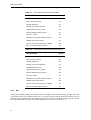
Contents
1 Introduction
1
2 Assignment Interpretation
3
2.1
2.2
2.3
2.4
Bus Interface .......................................................................................................3
User Interface ......................................................................................................3
Functions .............................................................................................................3
Components to Use .............................................................................................3
3 Bus Protocol
5
4 Protocol for Communication with the Terminal Card
7
4.1
4.2
4.3
4.4
4.5
4.6
Transfer of Identification Information ................................................................7
Transfer of the Menu Hierarchy ..........................................................................7
Transfer of Values and Actions ..........................................................................9
Transfer of LED Status .......................................................................................9
Transfer of Error Information ...........................................................................10
Summary of Address Usage ..............................................................................11
5 Terminal Card Hardware
5.1
5.2
5.3
5.4
5.5
5.6
Introduction .......................................................................................................13
Component Description ....................................................................................13
Securing Quality Design ...................................................................................18
Testing ...............................................................................................................19
Known Errors ....................................................................................................20
Changes .............................................................................................................21
6 Terminal Card AVR Software
6.1
6.2
6.3
6.4
6.5
6.6
6.7
6.8
6.9
6.10
6.11
13
23
Introduction .......................................................................................................23
Background .......................................................................................................23
Menu System .....................................................................................................24
Memory System ................................................................................................25
Bus Communication ..........................................................................................32
UART Interface .................................................................................................32
The Code Modules ............................................................................................33
Problems ............................................................................................................38
Testing ...............................................................................................................39
Changes .............................................................................................................42
Known Errors ....................................................................................................42
7 Terminal Card FPGA Design
7.1
7.2
7.3
7.4
7.5
7.6
7.7
7.8
43
Introduction .......................................................................................................43
Address Decoder ...............................................................................................43
LED Controller .................................................................................................47
Interrupt Register ..............................................................................................48
Bus Controller ...................................................................................................48
Bus Master ........................................................................................................60
Simulation .........................................................................................................61
Known errors .....................................................................................................63
8 Terminal Card Hardware and Software Integration
65
8.1 Introduction .......................................................................................................65
8.2 Integration .........................................................................................................65
9 DSP Card Hardware
9.1
9.2
9.3
9.4
9.5
9.6
9.7
9.8
9.9
9.10
Introduction .......................................................................................................68
The Printed Circuit Board .................................................................................69
DSP Part ............................................................................................................70
FPGA Part .........................................................................................................73
XChecker and SPROM .....................................................................................74
Other Components ............................................................................................75
Configuration ....................................................................................................75
Problems ............................................................................................................79
Testing ...............................................................................................................80
Changes .............................................................................................................80
10 DSP Card FPGA Design
10.1
10.2
10.3
10.4
10.5
10.6
10.7
10.8
83
Introduction .......................................................................................................83
Basis for Design ................................................................................................83
Description of the Top Level Design ................................................................85
Description of the Blocks of the FPGA Design ................................................88
Problems ..........................................................................................................107
Testing .............................................................................................................107
Changes ...........................................................................................................116
Known Errors ..................................................................................................117
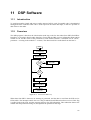
11 DSP Software
11.1
11.2
11.3
11.4
11.5
11.6
67
119
Introduction .....................................................................................................119
Overview .........................................................................................................119
Program Organization .....................................................................................120
The DSP Sound Modules. ...............................................................................121
The SHI Handling Routine .............................................................................124
Interrupt Routines ...........................................................................................125
11.7 Communication Between DSP and FPGA ......................................................126
11.8 Problems ..........................................................................................................126
11.9 Testing .............................................................................................................127
11.10Known Errors .................................................................................................129
12 DSP Card Hardware and Software Integration
131
13 Tools
133
13.1
13.2
13.3
13.4
13.5
13.6
13.7
13.8
13.9
Xilinx Foundation Series 1.4, Xilinx ..............................................................133
VeriBest 98, VeriBest Inc. ..............................................................................133
AVR Studio 1.42, Atmel Corp. .......................................................................134
Wavrasm 1.21, Atmel Corp. ...........................................................................134
AVR Macro Assembler 1.21, Atmel Corp. .....................................................134
AvrProg 1.25, Atmel Corp. .............................................................................134
BitCalc 3.0e, Cypress/IC Designs ...................................................................134
EVM56k ver. 1.06.00, Domain Technologies Inc. .........................................134
ASM56000 Assembler ver.6.1.0, Motorola Inc. .............................................135
14 Final Notes
137
14.1 Time Schedule for the Last Period ..................................................................137
14.2 Status ...............................................................................................................137
15 Conclusion
139
15.1 Problems ..........................................................................................................139
15.2 Guidance .........................................................................................................139
15.3 Experiences .....................................................................................................140
16 Bibliography
141
1 Introduction
The assignment was to design two cards named DSP card and terminal card. These cards should be
designed to communicate using an external bus defined by the Computer Architecture and Design
group.
The system was meant to act as a general sound processing system, with the ability to implement a vast
number of special filters and sound effects. The system have, with the right software, the ability to
decode surround data such as Dolby AC-3 from Dolby Laboratories and DTS (with some quality limitations) from Digital Theater Systems.
The purpose of the DSP card is to process sound by adding one or more effects or filters to the digital
sound signal, and produce three output stereo sound channels. Inputs and Outputs can either be analog
or digital. The digital signal processing is done using a DSP from Motorola connected to an external
SRAM. The internal control on the card is done using an FPGA form XILINX.
The purpose of the terminal card is to act as a controlling unit for cards connected to the external bus.
This includes being the bus controller and the user interface for the other cards. The user interface consists of a menu hierarchy obtained from the controlled card. Communication with the menu system is
done using a display, a 16 button keypad and five extra buttons. In addition to the menu hierarchy, the
card under control is asked to show information on 12 colored LEDs. The processing on the terminal
card is done using an AVR microcontroller from Atmel, and an FPGA from XILINX is used as the bus
master, bus interface, LED controller and address decoder for an internal bus.
The project has been carried out as four concurrent sub-projects; DSP card hardware design, DSP card
FPGA/software design, Terminal card hardware design and Terminal card FPGA/software design. This
has been a new experience for the students and has required a high degree of co-operation. Agreements
had to be made about the fundaments of the design, such as protocols and the relationship between the
hardware and the software.
1
DM Project 1998
2
2 Assignment Interpretation
Two card is to be constructed which together will form a system capable of processing digital and analog sound information using a digital signal processor. The two cards is called Terminal card and DSP
card. The terminal card acting as the user interface and bus master and the DSP card doing the sound
processing.
2.1
Bus Interface
The two cards will be attached to an external bus of type Compact PCI and has to follow the protocol
specified by the Computer Architecture and Design group. This protocol is summarized in Section 3
Bus Protocol.
2.2
User Interface
The terminal card provides the interface for the user to control the system. Therefore it is equipped with
a display, two times six LEDs, a keypad with sixteen keys and five independent buttons not including a
reset button.
2.3
Functions
2.3.1 Terminal Card
Provide the user interface for all cards connected to the external bus regardless of their function. This is
done using a flexible menu system which the terminal card requests from the other cards. All cards will
be asked by the terminal card to identify themselves.
The card will function as the bus master on the external bus, implemented in the FPGA.
Components on the card will be connected using an internal bus. The address decoder will be implemented in the FPGA in addition to a LED controller.
2.3.2
DSP Card
The card will control the level of two input channels and six output channels and it will be possible to
add sound effects implemented in the DSP.
2.4
Components to Use
2.4.1 Terminal Card
•
•
•
•
•
•
AVR microcontroller from Atmel
FPGA from Xilinx (4044)
XChecker and SPROM for configuration of the FPGA
LCD display
Keypad decoder
Keypad with sixteen keys
3
DM Project 1998
•
•
•
•
Five buttons
LEDs
RS232 serial port
HP pods for hardware debugging
2.4.2
•
•
•
•
•
•
•
•
•
4
DSP Card
DSP 56007 (Digital Signal Processor) from Motorola
OnCE interface for programming and debugging of the DSP
RAM for use with the DSP (16 bit address, 8 bit data)
Codec (AD/DA plus filters)
FPGA from Xilinx (4044)
XChecker and SPROM for configuration of the FPGA
AES/EBU used for receiving and transmission of digital sound
RS232 serial port
HP pods for hardware debugging
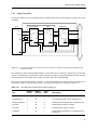
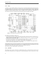
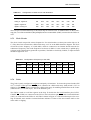
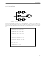
3 Bus Protocol
The bus protocol defines how the exchange of data is done on the external bus. A data packet consists
of one address word and a free number of data words. The first word of a packet is the address word.
The four least significant bits of the address are used for card addressing. When all four bits are set, the
packet is a broadcast message. This implies that only 15 cards can be addressed.
Mode bit
24 bit internal card addressing
8 bit
8 bit
8 bit
Not
used
Card
address
3 bit
Address word
4 bit
31
0
4th byte
3rd byte
2nd byte
1st byte
8 bit
8 bit
8 bit
8 bit
31
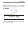
Figure 3–1:
Data word
0
The format of the address word and data word exchanged
between the cards connected to the external bus
Bit four, the mode bit, is used to indicate if there are one or more words sent to the same address. Three
bits are reserved for future use. The remaining 24 bits are used for internal addressing. See Figure 3–1
how the format looks.
A cleared mode bit indicates single mode transmission, while a set mode bit indicates burst mode. In
single mode one address word and one data word are transferred, while in burst mode a number of data
words are transmitted.
32 data lines are used to exchange data between cards connected to the external bus. The data lines are
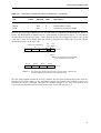
tri-stated to avoid more than one card to drive the lines. The start line indicates the start of a packet. The
line is set when the first word is put on the bus. The stop line indicates the end of a packet. This line is
set on rising clock edge when the last word is put on the bus. All cards are tri-stated to the data lines
during arbitration. Both start and stop line is tri-stated and driven by the terminal card during arbitration. The card granted the bus drives these lines during data transfer. See more about the arbitration in
section 7.6 . See Figure 3–2 for an illustration of the timing of the signals.
All cards can request the bus. Each card has its own request line except the card mastering the bus. If
this card is to request the bus, it must implement an internal request line. The card uses this request line
to indicate that it wants to put data on the bus. The bus has a total of seven request lines. The bus is
granted the card with the lowest address, having a request signal set one clock cycle prior to arbitration.
Four grant lines are controlled by the terminal card and indicate which card is granted the bus. All cards
not granted the bus have to wait for the start line set. When it is set, all cards have to read the address
word. This word has to match the cards address to make it read consecutive words on the bus. The stop
line is set when the last word is on the bus and the card stops reading on falling clock edge. All writing
is done on rising clock edge, while reading is done on falling clock edge.
5
DM Project 1998
CLK
Data
DATA
DATA
DATA
ADDR
DATA
DATA
DATA
START
STOP
REQ4
REQ6
GRT3
GRT2
GRT1
GRT0
Figure 3–2:
6
An example showing the timing of the bus protocol.
ADDR
DATA
DATA
DATA
4 Protocol for Communication with
the Terminal Card
A protocol for communication between the terminal card and other cards has been specified. This protocol limits how the terminal card can control cards on the bus, and therefore it is made flexible.
Information to be transmitted is devided into four categoris. This information is transmitted betveen the
terminal card and other cards in the system; identification, the menu hierarchy, LED status and error
information. The addresses FFFF00h to FFFFFFh have been reserved for this communication.
4.1 Transfer of Identification Information
1. The terminal card asks all card to identify itself by sending a packet to address FFFFFFh.
2. The cards answers by sending a packet to address FFFFFFh on the terminal card containing a name
of12 bytes (three data words) using 8-bit ASCII format, see Figure 4–1.
FFFFFFh
XXX1b
0h
Name (4 bytes)
Name (continued) (4 bytes)
Name (continued) (4 bytes)
Figure 4–1:
Format of the identification packet
The ID request must not be ignored if the card is to be identified by the terminal card. The terminal card
sends a broadcast asking for information packets, and uses the returned information to identify which
cards are installed in the system. A name of at least one character has to be supplied. The first byte has
to be different from 00h.
4.2
Transfer of the Menu Hierarchy
A menu consists of a hierarchy in three levels. Every menu item can have one of three actions when
chosen; go down to the next level, execute a command or change a value. When the menu item is used
for changing a value, it is also possible to show the current value by requesting this information from
the card in question. This value can be a 16-bit number that is in the range [0, 65536] decimal or [0,
FFFF] hexadesimal. When setting a new value, the value must always be a number from zero to a given
maximum value.
The menu item has a unique position in the menu hierarchy of a specific card. This position is called a
menu level. A menu level is described by two bytes. Of these two bytes the most significant five bits
describe the position at the highest level, the next five bits describe the position at the middle level and
the least significant six bits describe the position at the lowest level.
Table 4–1 shows an example menu with menu level codes. At the highest level three menu items X, Y,
Z and W is shown. X and Y have no items below themselves, therefore the middle and low level codes
are set to 1. Z has two menu items below itself, Z1 and Z2. Z1 and Z2 have no menu items below themselves and the code for the lowest menu level are set to 1. W also has two menu items below itself, W1
and W2. Each of W1 and W2 also have two menu levels below themselves.
7
DM Project 1998
Table 4–1:
Example menu
Description
Menu level codes
High
5 bits
(dec)
Middle
5 bits
(dec)
Low
6 bits
(dec)
X
0
1
1
Y
1
1
1
Z
2
0
0
Z1
2
1
1
Z2
2
2
1
3
0
0
3
1
0
W1-1
3
1
1
W1-2
3
1
2
3
2
0
W2-1
3
2
1
W2-2
3
2
2
High
level
Middle
level
Low
level
W
W1
W2
4.2.1 Three Types of Actions
When the low level code is zero:
• The menu item leads down to the next level. If the menu item is at the top level, then the middle
level codes is zero as well.
When the low level code is not zero:
• When the maximum value is set to zero the menu item executes a command when chosen.
• When the maximum value is not set to zero, the menu item sets a value.
See Table 4–1.
4.2.2
The Menu Hierarchy Transfer Process
1. The terminal card asks a card to send the menu hierarchy of the card, by sending a packet to address
FFFFFDh.
2. The card in question answers by sending the first menu item with information on where in the hierarchy that menu item has its place, a maximum value if the menu item has a value attached to it and
a name, to address FFFFFDh on the terminal card, as Figure 4–2 shows.
8
Protocol for Communication with the Terminal Card
FFFFFDh / FFFFFCh
XXX1b
Menu codes (5+5+6 bits)
Maximum value (16 bits)
Name (4 bytes)
Name (continued) (4 bytes)
Figure 4–2:
0h
Format of the menu item packet
3. After receiving the first menu item, the terminal card continues requesting more menu items by
sending packets to address FFFFFDh.
4. The last menu item is sent to address FFFFFCh on the terminal card. In this way, the card in question
signals that the whole menu is transferred.
5. The menu hierarchy has to be transferred in this order: the first item of the highest level, the items on
the levels below this item and then the second item on the high level and so on, see Table 4–1.
The menu request should not be ignored. To signal that the card does not have a menu a packet is sent to
address FFFFFBh on the terminal card as an answer to a menu request.
4.3
Transfer of Values and Actions
This transfer uses the format in Figure 4–3. Because these packets requests or contains parameter settings, they should not be ignored.
FFFFFAh / FFFFF9h
Menu codes (5+5+6 bits)
Figure 4–3:
XXX0b Cardn
o
Value (16 bits)
Format of the value transmission packet
1. To request a value, the terminal card sends a packet to FFFFFAh on a card.
2. The reply is sent to the address FFFFF9h on the terminal card.
1. To tell a card that a new value has been set it sends a packet to FFFFF9h on the card.
2. A reply is not sent to the terminal card.
1. To tell a card that an action has been executed, the terminal card sends a packet to FFFFFAh on a
card, not using the value part of the format in Figure 4–3.
2. A reply is not sent to the terminal card.
4.4
Transfer of LED Status
1. The terminal card requests LED status information from a card by sending a packet to address
FFFFFEh.
9
DM Project 1998
2. The card in question answers by sending a packet to FFFFFEh on the terminal card. This packet
contains a bit pattern describing which LEDs are to be turned on, using one bit for each LED, shown
by Table 4–2 and Figure 4–4.
Table 4–2: The LEDs on the terminal card
L (left)
R (right)
red
red
yel(low)
yel(low)
gre(en)1
gre(en)1
gre(en)2
gre(en)2
gre(en)3
gre(en)3
gre(en)4
gre(en)4
FFFFFEh
XXX0b
0h
Unuse L
L
L
L
L
L Unuse R
R
R
R
R
R
Unused
d (2 red yel gre1 gre2 gre3 gre4 d (2 red yel gre1 gre2 gre3 gre4
(16 bits)
bits)
bits)
Figure 4–4: Format of LED status package
The LED request can be ignored.
4.5
Transfer of Error Information
It is possible to transfer error information to the terminal card. This information will be shown to the
user. The message is transferred using 12 bytes of data in 8-bit ASCII-format, to address FFFFFAh on
the terminal card, see Figure 4–5 for illustration.
FFFFFAh
Message (4 bytes)
Message (continued) (4 bytes)
Message (continued) (4 bytes)
Figure 4–5:
10
Format of the error information packet
XXX1b
0h
Protocol for Communication with the Terminal Card
4.6
Summary of Address Usage
Addresses for communication between the terminal card and other cards is shown in Table 4–3 and
Table 4–4.
Table 4–3:
Messages to the terminal card
Data words (most significant part described first)
Address
(hex)
Description
1st
FFFFFF
Identification
Name of card
FFFFFE
LED value
LED level
[not used]
FFFFFD
Menu hirearchy
(one menu item)
Menu level code,
max value
Menu item description
[not used]
FFFFFC
Menu hierarchy
(last menu item)
Menu level code,
max value
Menu item description
[not used]
FFFFFB
No menu
[empty]
[not used]
[not used]
[not used]
FFFFFA
An error
Error message
FFFFF9
A current value
Menu level code,
current value
[not used]
[not used]
[not used]
Table 4–4:
2nd
3rd
4rd
[not used]
[not used]
[not used]
Messages from the terminal card
Data words (most significant part described first)
Address
(hex)
Description
1st
2nd
3rd
4rd
FFFFFF
Identification
request
[empty]
[not used]
[not used]
[not used]
FFFFFE
LED value request
[empty]
[not used]
[not used]
[not used]
FFFFFD
Menu item request
[empty]
[not used]
[not used]
[not used]
FFFFFC
FFFFFB
Reserved
FFFFFA
Current value
request
Menu level
[not used]
[not used]
[not used]
FFFFF9
Set a new value
Menu level code,
new value
[not used]
[not used]
[not used]
11
DM Project 1998
12
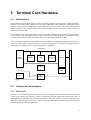
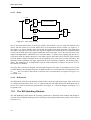
5 Terminal Card Hardware
5.1
Introduction
The terminal card is the users interface to the system. By using the keypad and five additional buttons,
the user can set and modify parameters on the cards connected to the external bus. Information about
the other cards on the bus is displayed on an LCD display as a set of menus. The card is equipped with
LEDs arranged in two columns which can be used to indicate various parameters, such as volume or
balance on an audio card.
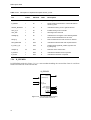
The terminal card is also the bus master. Every bus request is handled by the master, and grant signals
are given to the card with highest priority of those cards having requested the bus. The bus clock is generated by the terminal card. The frequency can be set in the range 1 MHz to 33 MHz.
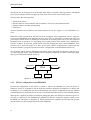
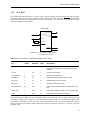
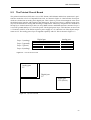
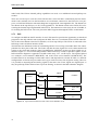
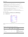
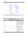
The bus master is implemented in an FPGA. A microcontroller is managing the display and keypad. An
overview of the system is shown in Figure 5–1. In the following sections, all major components will be
described in more depth. See also circuit schematics in Appendix A.
Internal bus
SRAM
LCD
Keypad
FPGA
External bus
Microcontroller
buttons
LEDs
Serial
port
Figure 5–1:
controll
Clock
generator
clk
Terminal card system overview
5.2
Component Description
5.2.1
Xilinx FPGA
An FPGA, or a ”Field Programmable Gate Array” is an integrated circuit which can be configured in
various ways. Shortly described, it consists of internal logic blocks, input and output blocks, and an
interconnection grid connecting the blocks and buffers. The logic blocks provide the functional elements for constructing the user’s logic, and the input and output blocks provide the interface between
the package pins and internal signal lines.
13
DM Project 1998
The FPGA used in the design is an XC4044XL from Xilinx. It contains 1600 logic blocks with 44000
gates, and is complex and fast enough to provide a base for the tasks needed in the project.
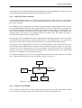
The FPGA has the following tasks:
•
•
•
•
External bus master
Interface between microcontroller and external bus, with receive and transmit buffers
Data bus address decoding and signaling
LED Driver
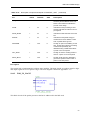
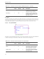
All these functions are described in the Xilinx software section. See Figure 5–2 for a functional overview.
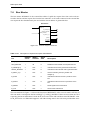
When the system is powered up, the FPGA must be configured. The configuration source is either the
on-card serial EEPROM or the Xchecker interface. The source is selected by a switch on the PCB. On
power-up the FPGA checks its MODE pins to determine its operating mode. These pins are connected
through resistors to ground or Vcc, depending of the switch position. If the switch is set to SPROM, the
FPGA is in Master Serial mode, and the FPGA reads the configuration from a serial EEPROM. If the
switch is set to XChk, the FPGA is in Slave Serial mode, and the configuration is loaded from the
XChecker interface. Using the XChecker interface, configuration can be downloaded from a PC.
The XChecker can be used for debugging if the FPGA design and hardware supports it. We are, however, not using this feature. After the FPGA has been properly configured, it will set its DONE pin high,
and a green LED marked DONE will be lit.
SPROM
XChecker
Internal bus
External bus
FPGA
Buttons
Figure 5–2:
5.2.2
LEDs
Functional overview of the FPGA
FPGA Configuration Serial EEPROM
Because the configuration of the FPGA is volatile, it must be downloaded every time the power is
turned on. It may be acceptable to use the XChecker interface during the development of a design, but
eventually, it is preferable that the FPGA automatically will load the configuration from the onboard
serial EEPROM. As mentioned, this is the case if the download mode switch is in the SPROM position.
When power is applied, the FPGA is initialized. During this phase, the INIT pin on the FPGA goes low.
This pin is connected to the EEPROM pin RESET/OE, thereby reseting the address counter in the
EEPROM (see schematics in Appendix A). When initialization is complete, the INIT pin will go high,
and the FPGA can start clocking in data from the EEPROM.
14
Terminal Card Hardware
The DONE pin is low during initialization and configuration. When configuration is complete, this pin
will go high and disable the EEPROM, and the DONE LED will be lit.
5.2.3
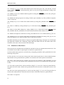
Atmel AVR Microcontroller
A microcontroller handles the access to the keypad and the display. In this project it is a AT90S8515
microcontroller from the AVR series produced by Atmel. Other cards must access the keypad and display via the controller.
The AT90S8515 microcontroller provides 8KB of reprogrammable FLASH program memory, and 512
bytes of data EEPROM, which both can be programmed in-system by a serial interface. A program can
be loaded into the AVR by plugging an AVR ISP programmer to the ISP plug. The controller has 512
bytes of internal SRAM, and an external bus interface which can address 64KB external SRAM. The
external memory bus interface uses multiplexed data and address pins. The address low byte is
extracted from the bus by using an address latch.
In this design, an extra 32KB SRAM chip is connected to the external bus for greater software flexibility. This allows the AVR software to store large data structures. The SRAM used is a 70 ns version with
a three-line control scheme. All bus timing requirements are satisfied without additional logic.
Asynchronous serial communication with the card is possible through a connector located at the card.
The communication is handled by the controllers on-chip UART. By using this feature, the card can be
connected to a PC for testing purposes or as an extra interface. The AVR is clocked by a 3.6864 MHz
external crystal (This is not the external bus clock generator!). With this frequency, all common baud
rates up to 115 200 baud can be generated accurately.
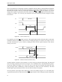
Two external interrupts provide a way for the keypad and the FPGA to notify the controller of incoming
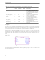
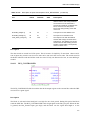
data. A functional description of the microcontroller is shown in Figure 5–3.
ISP
Internal bus
Serial
port
AVR
clock
Crystal
Figure 5–3:
5.2.4
control
Clock
generator
Functional description of the AVR microcontroller
Liquid Crystal Display
A 2×16 character LCD module is used to display the menus provided by other cards on the external
bus. It is also used to display settings and menus which are local to the terminal card.
15
DM Project 1998
The LCD module has an integrated controller compatible with the industry standard Hitachi HD44780.
This controller is however not well suited for interfacing to the AVR external memory bus. It utilizes a
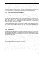
Motorola bus interface with an E clock and combined R/W control signal (see Figure 5–4). In our
design, these signals are generated by the FPGA based on the RD and WR signals from the AVR microcontroller (see Figure 5–5). This way, the controller can access the display directly using the external
bus interface.
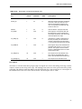
RS
RS valid
R/W
PW en
E
tDSW
Data valid
Data
Figure 5–4:
th
LCD Bus Interface Timing
For simplisity, the LCD R/W signal is put low. This implies that the AVR will not be able to read status
information from the LCD. One of the reasons for reading the display is to check if it is ready to receive
new data. This however, can be solved by making the AVR wait the required amount of time before
issuing a new write.
Address
Address valid
PW WR
WR
tH
Data
Figure 5–5:
Data valid
AVR Microcontroller Bus Interface Timing
Another problem is that the LCD controller is to slow to keep up with the AVR timing. The data hold
time for writing required by the LCD (th in Figure 5–4) is minimum 20 ns. The data hold time guaranteed by the AVR (tH in Figure 5–5) is 0 ns. One way to solve this is to latch the data when the write
pulse goes high. This is handled by a latch on the board (see latch U6 on the schematics). The latch
enable signal is generated by the FPGA. See also FPGA software description.
The last problem is the length of the enable pulse to the LCD (PWEH in Figure 5–4). The enable pulse
is generated by the FPGA, and is based on the WR signal from the AVR. This pulse must be longer than
16
Terminal Card Hardware
280 ns. The WR pulse is however not long enough under normal operation (PWWR in Figure 5–5). By
introducing one wait-state for the AVR when accessing external memory, the WR pulse will be
stretched one cycle. With a 3.6864 MHz crystal frequency, the WR pulse will now be minimum 386 ns.
The display contrast is set by a voltage at the VO pin of the display. This voltage has to be in the range
0–1.2 V. The contrast can be adjusted by turning a potentiometer (se R109 on the schematics).
5.2.5
System Clock Generator and Clock Buffer
A clock generator is used to generate the clock for the FPGA and the external bus. The clock generator
used in this design is a IDC2053B from Cypress. It is capable of generating a clock output frequency in
the range 391 kHz to 90 MHz, with a rise and fall time of 1 ns/V. A steep edge on the system clock signal is important for correct operation of other cards in the system on high bus frequencies.
The generator is programmed by shifting in a bit stream, containing information about the clock frequency. This is done by the AVR. The user can select between preset frequencies from the System
Menu. The generator is capable of changing output frequency without glitches. This allows the frequency to be changed while the system is running.
If the the maximum of eight cards are connected to the external bus, terminal card included, a capacitive load of up to 80 pF will be added to the system clock path. The output driver of the generator is not
able to drive the clock at 33 MHz under such conditions. To solve this problem, a clock buffer is
inserted between the generator and the external bus. This buffer satisfies our requirements: It is able to
drive 8 cards, each card having an input impedance of 10 pF. The rise/fall times at this load is specified
to be 1.0 ns/V or better, keeping the clock signal sufficiently squared.
5.2.6
Serial Interface
As mentioned, serial communication with the AVR microcontroller is possible using the UART on the
chip. To be able to connect the card to a PC or other RS-232 compatible equipment, the 5V logic levels
from the AVR have to be converted to standard RS-232 signal levels. This is handled by a RS-232
driver MAX202 from Maxim.
The AVR UART transmit and receive lines are connected to the driver, and the RS-232 level signals are
available at the serial connector on the board. The voltage needed for the RS-232 signal levels are generated by the chip itself, eliminating the need of extra voltage sources.
An RJ-11 modular plug is used for the serial interface. This plug is chosen instead of a standard D-SUB
plug because it is smaller and is easier to mount. Also, it does not put so much stress on the card as a
D-SUB would, when plugging and un-plugging the connector.
5.2.7
Keypad
The keypad used is a 16-button keypad arranged in a 4×4 matrix. It is connected to a keypad decoder.
The keypad decoder is the interface between the keypad and the AVR. It is connected to the data bus
and is addressed like any other memory location. The decoder features a Data Available signal which is
connected to the AVR interrupt line INT0. When a key is pressed, this signal goes high, and generates
an interrupt in the AVR. This indicates that data can be read from the bus.
17
DM Project 1998
The keypad select signal, indicating that the decoder is to put data on the bus, is generated by the FPGA
when the proper combination of the bus address and the RD signal from the AVR exists.
As for the LCD, the timing requirements for the keypad decoder is not satisfied under normal operation. By introducing one wait-state in the AVR when accessing the keypad, the RD pulse will be
stretched one cycle, and the timing requirements are held.
5.2.8
Buttons
The AVR can be reset by pressing the button marked AVR Reset. Pressing this button, the reset signal is
pulled low, activating the reset. The FPGA and the other cards connected to the external bus are reset by
pressing the button marked Bus Reset. This provides a mechansim to reset cards on the external bus
when a card seems to have ”chrashed”, or the operation on the external bus is jammed by long (un-ending) data packets. (See the switches SW1 and SW9 on the schematics, respectively).
The five big blue buttons are connected to both the AVR and FPGA. Pull-up resistors are pulling the
signal level high when the buttons are not pressed. Pushing a button connects the signal to ground, pulling it low.
The buttons have at the moment no function in the FPGA design, but can be used for debugging purposes or in new designs using the same hardware. They are considered used as “navigation buttons” for
the user interface, but so far the keypad seems to make these buttons redundant.
5.2.9
The External Bus Interface
The external bus is compatible with the Compact PCI standard. The bus provides more than enough
signal lines for our design. All cards on the system is mounted in a rack, using the Compact PCI bus as
a the backplane bus.
A Compact PCI plug is mounted on one edge of the terminal card. The terminal card is mounted at the
front of the rack and connects to the bus with a cable. The power for the card is supplied via this plug.
As mentioned, the clock signal on the bus is provided by the clock generator on the terminal card.
5.2.10
Debugging Interface
The AVR memory data bus and the enable signals for the devices which are connected to it, are available at two connectors (Pod Connectors 1 and 2) on the board (See J6 and J7 on the schematics). They
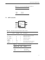
are intended to be connected to a logic analyzer, and are useful during debugging of the design. The signals on pod connector 1 are the bus address signals A[8-15], and the RD and WR signals. Pod 2 contains the data signals AD[0-7], and signals for the various devices on the internal bus.
5.3
Securing Quality Design
Errors or bad functionality on the final board can have several reasons. The most probable sources are:
•
•
•
•
•
18
Logical errors in the circuit construction
Connecting erroneously when drawing the circuit in Design Capture
Wrong or incomplete routing in the PCB editor (due to not updated netlist or component database)
Misunderstandings or errors when delivering board description to the manufacturer
Defective components, bad soldering or board defects
Terminal Card Hardware
Securing quality is important during the entire process when constructing the board. Logical errors in
the circuit construction can be avoided by achieving complete knowledge about every part of the circuit, by studying data sheets and having a good general knowledge to electronics. The final circuit construction must be examined and verified several times, and by several members of the group. The final
circuit drawing must be examined in the same way.
When the card is about to be routed, it is important that all netlists, component databases etc. are
updated to the last version of the circuit drawing. If this is not the case, incorrect routing or other errors
may not be discovered by the PCB software. When the placement of components and routing are finished, tests concerning netlist, component placement, track clearance etc. must be performed. When the
board description is sent to the manufacturer, all dimensions on tracks, pads, drill holes and silk print
must be verified.
5.4
Testing
5.4.1 The Schematics
The finished circuit schematics was examined by several members of the group. The issues of concern
were:
•
•
•
•
Power to all components
Signal levels
Bus timing
Noice (de-coupling capacitors at all integrated circuits)
All these issues were verified before the circuit was routed in the PCB editor. Some errors were discovered after the routing had begun, but were corrected and forward-annoteted. This made it possible to
continue routing without re-routing the whole board.
5.4.2
The PCB Layout
The PCB layout was mainly verified by running the tests mentioned in the “Securing design quality”
chapter, assuming that the schematics were correct at this point. A visual test was also performed on
issues like track clearance, clearance between pads and tracks, and signal tracks (re-routing tracks that
were unneccessary long or othervise strangely routed by the auto-router).
5.4.3
The Circuit Board
When the finished board was returned from the manufacturer, certain issues were tested:
• Connection between power pads at all integrated circuits and the power supply lines at the Compatc
PCI connector.
• Certain critical signals like external bus clock, AVR clock and signals used to program the AVR anf
the FPGA
• Conductivity of traces near the board edge
19
DM Project 1998
5.4.4
The Final Board with Components
The most critical components were monted first, one at a time. This gave us the option to test connections at a specific component. The following issues were tested:
• Component orientation
• Soldiering. On the most critical components all pins were probed, verifying that all were properly
soldiered, and that no pins were short-circuted to the closest pins
5.4.5
Testing the board with software
Testing the board with test software loaded into the AVR and the FPGA proved an effective method of
testing the final design. Test software was written to test these issues:
•
•
•
•
•
•
•
AVR programmability from the ISP connector
SRAM access from the AVR
LCD access from the AVR
Keyboard decoder access from the AVR
Clock generator access and programmability from the AVR
LEDS access from the FPGA
FPGA access and programmability from the XChecker cable
5.5
Known Errors
Even though the final circuit drawings are closely examined, errors sometimes unfortunately escape the
verification process. This chapter lists the errors that were known at the time the report was written
5.5.1
Wrong Silk Print Dimensions
On the final cards, the silk print is hardly visible. The reason for this is that the dimensions of the lines
of the silk print were wrongly specified. The manufacturer could not print the silk screen with a good
result at these dimensions.
5.5.2
Incorrect Hole Dimensions
By a mistake, the dimensions on the holes of the Compact PCI connector were set to be larger than the
size of the corresponding pads. The error occured when the description of the card was sent to the manufacturer, and was detected when the holes were about be drilled. The manufacturer contacted the
project group, which acknowledged that the diameter of the hole was wrong, and should be corrected.
Unforunately, all other holes with the same dimensions were modified as well. This has lead to extra
work, but has not affected the functionality of the card.
Patch: Adjust components so that they fit in the holes.
Correction: Correct the hole dimensions for the CPCI connector and generate new drill-list.
20
Terminal Card Hardware
5.5.3
Address Bus Contention
When the circuit was drawn in Veribest Design Capture, the pin AD4 from the AVR was, by a mistake,
connected to line AD[3] on the internal bus. Because of this, the AVR pins AD3 and AD4 was connected at the final board, and line AD[4] on the internal bus was not connected to the microcontroller.
The error was discovered when the address lines were probed with an oscilloscope.
Patch: Cut the connection between the pads of pin AD3 and AD4 on the AVR, and pin AD4’s connection to the internal bus. Strap AD3 and AD4 to their respective lines on the bus, e.g. AD3 to pin 86 on
the FPGA, and AD4 to pin 87.
Correction: Re-route the lines of interest in Design Capture, re-annotate, and route the pins once more
in the PCB editor.
5.5.4
Wrong Data Line Connected to the Keyboard
By a mistake, the line AD[7] on the internal bus is connected to the keyboard decoder pin 16. This pin
should, however, have been connected to AD[3].
Patch: Strap the line AD[3] to pin 16 on the decoder or patch the error in software, copying bit 7 to bit
3 in the read byte before processing the incoming keystroke.
Correction: Re-route data line 3 on the board in Design Capure, re-annotate and route the lines once
more in PCB editor.
5.6
Changes
When the final board was tested, the FPGA configuration could not be downloaded. This could have
two causes; the FPGA itself was not working correctly or there was an error on the board or in the
design that prevented the configuration download.
Further testing uncovered that the FPGA was causing the problem, and it was decided to replace the
chip. A new problem emerged because it was impossible to get hold of an FPGA of the same model. To
get a working, but somewhat reduced design, a smaller FPGA from the same Xilinx series has been
used on the final boards.
Using a smaller FPGA causes that some planned features in the FPGA has to be removed or reduced.
E.g, this concerns some internal buffers used to receive and transmit data from/to the external bus.
21
DM Project 1998
22
6 Terminal Card AVR Software
6.1
Introduction
The task was to design the software for the AVR AT90S8515 microcontroller of the terminal card. On
this card, the AVR controls the internal bus, reads the keypad, writes to the LCD, LEDs and clock generator, and write to or read from the external bus via the FPGA-logic.
The AVR is responsible for displaying a menu system to the user. This menu system will enable the user
to see the names of all detected cards on the Compact PCI bus. When a card has been selected, a menu
system will be downloaded from that card and displayed on the LCD. The user will then be able to navigate through the menu of the chosen card, and the AVR will give feedback to that card from the choices
made by the user at the terminal.
6.2
Background
The AT90S8515 is an 8-bit microcontroller designed by ATMEL. This section will list some of the features of the AVR and a short text describing the use of these features on the terminal card and by the
AVR software.
6.2.1
Program Flash
The 8 KB Flash of the AVR is used for storing the program running on the chip. The length of one
instruction is 16 bits, limiting the number of instructions in the Flash to 4 K. This is sufficient, our program is estimated to be about 3 KB.
6.2.2
Internal SRAM
512 bytes of SRAM is available on the chip. This RAM is used when memory requirements exceed the
capability of the 32 registers. The use of the internal SRAM is described in section 6.4.2 .
6.2.3
External SRAM
The AVR supports up to 64 KB external SRAM. On the terminal card there is 32 KB external SRAM.
This RAM is used for storing the menu data of the card currently being controlled.
6.2.4
Internal Interrupts
• Timer Interrupt, triggered by the internal timer at specified intervals.
• UART Interrupt, triggered by incoming data in the UART interface.
6.2.5
External Interrupts
• Reset, triggered by the reset button on the terminal card.
• External interrupt pin 0, reserved as a keypad interrupt. Triggered when someone presses a key on
the keypad.
23
DM Project 1998
• External interrupt pin 1, reserved as an FPGA interrupt. Triggered by the FPGA, signalling a pressed
button or incoming bus transmission.
6.2.6
Multiplexed Address and Data Pins
The AVR is able to read and write 16-bit address and 8-bit data on two ports by multiplexing address
and data. Reading from and writing to external units is therefore quite simple and is done by storing the
address in two registers. Writing to or reading from this address is then done using a single instruction.
The ports are connected to the internal bus of the terminal card, making it possible to access external
SRAM and units.
6.2.7
UART Interface
The AVR UART interface will be used for an RS-232 interface on the terminal card. The use of this feature is described in section 6.6 .
6.3
Menu System
The menu on the AVR is designed in such a manner that the upper line of the LCD shows the header of
the menu the user is navigating at any given point. When a variable is being adjusted the name of the
variable will be displayed as a header.
The keys of the keypad are used in various ways for navigation of the menu system. The green key represents a positive input. The red key represents a negative input. One use of these keys is retrieving a
yes or no answer from the user. Another use is entering or exiting a menu. The ‘+’ and ‘-’ keys are used
as variable increment and decrement respectively. The ‘<-’- and ‘->’-keys are used for navigation of the
current level. Navigation of items at a spesific level is wrapped around at the end points of that level.
The number keys are used for entering spesific values when adjusting a variable. Such an input can be
confirmed by pressing the green key or be undone by pressing the red key.
The lower line of the LCD shows the current choice, which is changed by using the left and right
arrows. Making a choice is done by pressing the green key and stepping back is done by pressing the
red key. When the user is adjusting a variable, the lower line will display the value and range of the
variable or simply “yes/no” or “execute?” if the maximum value of the variable is one or zero respectively. The standard for the structure of the menu system is explained in Section 4.
Handling navigation of the menu system is somewhat complex given the low level of the code, the
required freedom of use and the simple datastructure used for storing the menu. In memory, the menu is
simply stored in blocks, each block starting with the two byte level code of a particular item. Next,
there is an eight byte chunk storing the ASCII values representing the name of the item. Last, there is an
optional two byte chunk used for storing the maximum value of the item. This chunk is only used when
the item is a leaf node. This results in each item block being 10 or 12 bytes long.
We considered solutions like binary trees, linked lists etc. There are two reasons why a simpler solution
was selected. First, a lot of pointers would have used a lot of memory. If double linked list had been
used, each item would have four bytes used for pointers, resulting in the fact that 30% of the space
occupied by a nonleaf node was reserved for pointers. Secondly, more complex code would demand
more codespace, of which we have only 8 KB available. The complex code would also be harder to
handle in low level language.
24
Terminal Card AVR Software
A graphical representation of the menu memory system used is given in Figure 6–1.
Block format:
2 bytes
8 bytes
2 bytes
Item Level
Item Text
Max Value
Optional
High
Mid
Low
5 bits
5 bits
6 bits
Block example:
2 bytes
8 bytes
2 bytes
08C1h
Delay
FFFFh
Optional
00001b
00011b
000001b
5 bits
5 bits
6 bits
Example of sequence of blocks:
Gain In
Echo
On/Off
Channel 1
Delay
Level
The sequence of blocks is a depth first scan of the menu tree
Figure 6–1: Menu Memory Organization
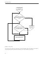
.A simplified overview of menu system navigation and program main flow is shown in Figure 6–2 to
Figure 6–5. In these figures, the symbols used represents keys on the keypad.The happy face represents
the green key while the sad face represents the red key.
6.4
Memory System
This subchapter explains the use of the memory space of the AVR. Memory is ranged from 0000h to
FFFFh, addressing a specific byte requires the use of two address bytes. This is usually done using the
upper register words X, Y and Z.
6.4.1
Memory Space
The memory space of the AVR has been divided into three categories. The internal memory of the AVR
is ranged from 0000h to 025Fh. I/O units are addressed 0260h to 7FFFh, and finally the 32 KB external
SRAM is addressed 8000h to FFFFh. The categories are listed in Table 6–1.
6.4.2
Internal Memory
The internal memory is used for storing data other than the menu system of the card being controlled.
The most important parts of data in the internal memory are the card memory, storing the names of all
connected cards, the display mirror, mirroring the contents of the LCD, the temporary memory, used for
storing procedure call data and other short-term usage and finally the data buffer which is used to store
up to 32 bytes of incoming data from the external bus.
25
DM Project 1998
Start
Initializing the AVR, testing the
Internal bus / Display
Memory
Internal bus / LED
External bus
Choose type
of menu
Choose type of
menu (AVR,
externald card)
×Ø
J
Type of menu:
AVR or external
card
AVR menu
Load the AVR
menu into the
memory.
Card=0
External card
L
Choose Card
Navigate the
Card
card=card±1 or
card={1,8}
L
×Ø
High level
navigation
×Ø
Choose high level menu.
high=high±1 or
high={0,1Fh}
J
Load the chosen
card's menu into the
memory
J
Node?
Yes
No
Menu
decoder
Mid level
navigation
Get
value
Figure 6–2: Main Navigation of Menu System, Part I
6.4.3
Memory Mapped I/O
As mentioned earlier, addresses 0260h to 7FFFh are reserved for I/O unit addressing. This limits the
maximum addressable external SRAM to 32 KB. This is not considered a problem given the expectations on reasonable menu size. The specific addresses of the units connected to the internal bus of the
terminal card is presented in Table 6–3.
6.4.4
Registers
The 32 registers of the AVR have been assigned to spesific purposes and are listed in Table 6–4. The
menu pointers store the current navigation position in the menu memory. The low, mid and high regis-
26
Terminal Card AVR Software
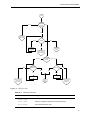
High level
menu
L
High level
navigation
J
Mid level
navigation
Choose mid level menu
mid=mid±1 or
mid={0,1Fh}
×Ø
Mid level
node?
Yes
Menu
decoder
Get
value
No
L
Choose low level menu
low=low±1 or
low={0,3Fh}
Low level
navigation
Change value
J
×Ø
Get
value
Menu
decoder
Figure 6–3: Main Navigation of Menu System, Part II
27
DM Project 1998
An input request
from the high, mid
or low menu
handling for a menu
item.
Test if the correct menu
item has been found. If not,
readjust the input and send a new
request.
Correct menu item
New request
Test if the high, mid and low
values of the last read menu item
are less than or equal to the
requested values.
Return to high,
mid or low
navigation.
Values too small, try next menu item
Values equal or greater
Get the next high, mid and low
values and decode them.
Figure 6–4: Menu Decoder
ters store the level code of the current item. In the card number register, the number of the card currently being navigated is stored. The last valid key press resides in the Key_Buf register.
28
Terminal Card AVR Software
Get
value
Type of value:
Execute?
Value
Yes/No?
Value?
Execute
Yes/No
Send
command
and return
×Ø
J
Yes/No
L
Send new
value and
return
Toggle the
item on/off
Return to
high, mid or
low navigation
Value type +/-
L
Change the
value with +/- Value type digit
or digit
Increment or
decrement
Next digit
J
L
J
[0..9]
±
write digit
digit=digit±1
Send
new
value
Return to high,
mid or low
navigation
Return to high,
mid or low
navigation
Figure 6–5: Getting the Value
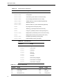
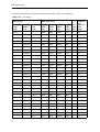
Table 6–1:
Memory Overview
Address
Usage
0000h-025Fh
Internal AVR memory
0260h-7FFFh
Memory mapped I/O (board units and external bus)
8000h-FFFFh
External SRAM of the AVR
29
DM Project 1998
Table 6–2: Internal Memory Addresses
Address
Usage
0000h-001Fh
Register File
0020h-005Fh
I/O Registers
0060h-00CFh
Card memory (The names of connected cards)
00D0h-00DFh
Error message (Received from other cards)
00E0h-00E1h
Variable memory L/H (the variable being adjusted)
00E3h-00EFh
Temporary memory
00F0h-00F1h
Maximum Value L/H (of the variable being adjusted)
00F2h
Key Flag (used for storing key state)
00F3h
Teststring_In (message received from the bus)
00F4h
Card_Error_Number (number of card reporting error)
0100h-0120h
Display Mirror (local memory mirror of the LCD screen)
0121h
Display Mirror Pointer (cursor pointer for the mirror)
0130h-0161h
Data Buffer (for buffering incoming data)
0162h-025Fh
Reserved Stack memory (158 bytes)
Table 6–3:
I/O Addresses
Address
Table 6–4:
30
Usage
0x7E00
Keypad
0x7E10
LCD Control
0x7E11
LCD Data
0x7E20
LED Left
0x7E21
LED Right
0x7E22
LED Both
0x7E30
FPGA Interrupt Register
0x7F80
External Bus Out Register
0x7FC0
External Bus In Register
Register Assignments
Register
Usage
Register
Usage
R0
Free usage, lpm target.
R16
Time
R1
Free usage
R17
Key_Buf
R2
Menupointer Low
R18
Temp (main)
Terminal Card AVR Software
Table 6–4:
Register Assignments
(continued)
Register
Usage
Register
Usage
R3
Menupointer High
R19
Temp 1
R4
Low
R20
Temp 2
R5
Mid
R21
Temp 3
R6
High
R22
Parameter 1
R7
Uart Low
R23
Parameter 2
R8
Uart High
R24
Parameter 3
R9
Flag Register
R25
Parameter 4
R10
Ticks
R26
X-low
R11
Digit
R27
X-high
R12
Temp 4
R28
Y-low
R13
Temp 5
R29
Y-high
R14
Temp 6
R30
Z-low
R15
Card Number
R31
Z-high
When performing procedure calls, parameters are stored in the parameter registers. The same registers
are also used for returning results to the caller. The X, Y and Z word registers are used for 16-bit
addressing. These registers have special support for word operations, and each is built up by two registers, e.g. Z consists of ZL and ZH, the low and high byte of Z. It is possible to store a byte at the location pointed to by Z and increase the word by one in a single instruction. The registers 24 and 25
support word operations as well. These registers have been reserved as parameters three and four. This
is an advantage since incoming parameters can be handled as words without moving them into other
registers. Register zero is the destination register when loading program memory using the instruction
lpm.
The Flag register is used for storing special information about the state of the system. The format of this
register is shown in Figure 6–6.
bit 7
bit 6
bit 5
bit 4
Item
value
error
timed out
received
received received
bit 3
menu
finished
bit 2
bit 1
no menu uart high
bit 0
uart low
Figure 6–6: The Flag Register
In the Flag register, the item received bit is set when an item has been requested and has arrived. The
timed out bit is set if the predefined timeout period has expired during a loop waiting for a card to send
information to the terminal card. Value received and Error received simply signifies if a value or error
message has arrived from a card. The menu finished is set if a menu has been requested and a Last
Menu Item pack has arrived from the external bus. No Menu is set if a menu has been requested, but the
target card replies with a packet stating that the card has no menu system. The final two bits are used for
the UART interface routines.
31
DM Project 1998
6.4.5
External Memory
The external memory on the terminal card is used for storing the menu system of the card currently
being navigated. 32 KB is sufficient for menu storage, limiting the maximum number of items to about
2700. The external SRAM is addressed 8000h to FFFFh.
6.5
Bus Communication
The standard for communication between cards is described in Section 4. The external bus communication of the AVR is at the moment limited to concepts within this standard, and therefore only a simple
overview of the logical ports of the AVR is given in Table 6–5 and of the logical ports written to by the
AVR is given in Table 6–6.
Table 6–5:
Port Addresses of the AVR
Address
Usage
FFFFFFh
Card ID
FFFFFEh
Set LEDs
FFFFFDh
Menu Item
FFFFFCh
Last Menu Item
FFFFFBh
No Menu
FFFFFAh
Error Message
FFFFF9h
Value
Table 6–6:
Ports Written to by the AVR
Address
6.6
Usage
FFFFFFh
Request ID
FFFFFEh
Request LED
FFFFFDh
Request Menu
FFFFFAh
Request Variable Value
FFFFF9h
Set Variable Value
UART Interface
A UART interface is designed to make communication between a PC and the terminal card possible.The interface is simple yet fairly flexible. Due to lack of time, no PC software has designed to
exploit the UART interface of the AVR. The concept of the interface is that the PC request a memory
byte by sending two address bytes, and the AVR replies by returning the contents of the memory at the
given address. The PC is also allowed to send its high byte equal to 50h, indicating that instead of doing
32
Terminal Card AVR Software
a memory read the PC wish to write a byte to the keypad buffer. The next byte sent by the terminal will
then be the byte to be written to the buffer instead of the low byte of an address.
The design makes implementation in low level code on the AVR quite simple, while more sophisticated
software is needed on the PC. The PC is able to image the memory of the AVR, do limited survey of
events, and emulating a key press, allowing remote operation of the terminal card. The simplicity of the
concept introduces a flaw, as the value 50h in the most significant byte of an address is reserved for key
emulation. This makes the PC unable to read the address area 5000h to 50FFh. This is not a serious
problem, since this address area is not currently in use.
6.7
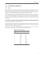
The Code Modules
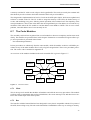
The assembly code has been organized into several modules to decrease complexity and increase modularity. The modules are presented later in this chapter. Parameters are contained in register aliases p1p5, and a procedure is presented in the format:
Procedurename(parameters)
Private procedures are called only from the same module, while all modules are able to call Public procedures in any of the other modules.This is only a logical categorization. There is no procedure protection. The source code is included in Appendix D.
An overview of the modules included in the main assembler file is given in Figure 6–7.
Display.Inc
Menu.Inc
Keyboard.Inc
Menu_D.Inc
Bus.Inc
Main.Asm
Utils.Inc
LED.Inc
Timer.Inc
UART.Inc
Globals.Inc
Figure 6–7: Inclusion Overview
6.7.1
Main
This is the top level module that includes all modules and calls the necessary procedures. The module
performs calls to components that requires initialization, does some start-up work, and then leaves control to the eternal loops of the menu system.
6.7.2
Bus
The interface with the internal bus has been designed in a way that is compatible with the I/O system of
the AVR, thus writing to any I/O unit on the internal bus is handled the same way as writing to memory.
33
DM Project 1998
On the other hand, the interface with the external bus needs some sort of code. This code is implemented in the Bus module. The module also fills the menu system block of the memory with menu data
arriving from the card currently being controlled.
PUBLIC PROCEDURES
Procedure Get_Cards()
Sends a broadcast with id-request
Procedure New_Card()
Gets the menu of card numbered #Card
Procedure Get_Value(item_l, item_h, value_l, value_h)
Gets a value from #Card
Waits for arrival of value (or time_out)
Procedure Set_Value(item_l, item_h, value_l, value_h)
Sets a value on #Card
Procedure LED_Request(ledcard)
Request LED info from #Card (no wait)
Procedure Bus_Interrupt:
Interrupt from the FPGA
Procedure Send_ID()
Transmits own ID to ext.bus.
PRIVATE PROCEDURES
Procedure Read_Bus()
Read current bus packet from FPGA
6.7.3
Display
The Display module handles interface with the LCD, supporting calls like writing characters and
strings at specific positions.
PUBLIC PROCEDURES
Procedure Init_LCD()
Initializes the display for 8-bit, 2 lines and auto incrementation.
Procedure Display_Char(x-pos, y-pos, Character)
Print one character to the LCD at pos (x, y).
Procedure Display_String(x-start, y-start, String_p_Low, String_p_High)
Prints character on the LCD from memory until string termination.
For writing messages to the LCD. I.g. Initializing and
error messages.
Procedure Display_String8(x-start, y-start, String_p_Low, String_p_High)
Prints 8 characters from memory to the LCD at pos (x, y),
String_pointer_low and String_pointer_high points to the place in
memory where the data is stored. String is unterminated.
34
Terminal Card AVR Software
Procedure Display_Card_label(x-start, y-start, String_p_Low,
String_p_High)
Prints 12 characters from memory to the LCD at pos (x, y). Used to
print the card label when traversering the cards.
Procedure Display_Constant(x-start, y-start, String_p_Low, String_p_High)
This procedure prints strings from program memory to the display at
position (x, y).
Procedure Clear_Display()
This procedure clears the LCD
Procedure Set_Cursor(cursor_on_?)
Turn the cursor marker on/off.
PRIVATE PROCEDURES
Procedure SET_CHAR_POS(x_pos, line)
Puts the cursor at position (x, y) on the LCD.
X = [0..15], Y = [0..1]
Procedure WR_LCD()
Write the character or command to the LCD.
6.7.4
Keypad
This module updates the key buffer each time the user presses a key. The key buffer stores only one
character. All keys pressed while the buffer is unequal to 00h are discarded.
PUBLIC PROCEDURES
Procedure Init_Keyboard()
Initilializes the keyboard
Procedure card_error_display()
Display received error message
Procedure Read_Key(key)
Read from keyboard (wait for key)
Procedure Keyboard_Int()
Keyboard interrupt handler
6.7.5
LED
Writing to the LED column is done using the procedures in the LED module. Each of the LEDs can be
set individually. These LEDs are usually set by the card being controlled.
PUBLIC PROCEDURES
Procedure Write_LED(Leftdata, Rightdata)
Writes to left and right LED column
35
DM Project 1998
Procedure Clear_LED()
Clear both LED columns
6.7.6
Menu
The Menu module introduces procedures for handling the navigation of the menu system at most levels.
And for setting new values to the menu item. The menu navigation is divided into 3 levels; High, Mid
and Low. The possibility of leaf nodes at High and Mid level complicates the menu memory navigation.
PUBLIC PROCEDURES
Procedure trav_card(card)
Choose Card
PRIVATE PROCEDURES
Procedure write_card_number(card)
Write the number of the card at the end of the line.
Procedure display_max_value(Menupointer_Low, Menupointer_High)
Display maximum value of menu item.
Procedure menu_get_value()
Gets the value from the card and test for timeout
Procedure adjust_bin2des(t1,t2,t3,t4,t5)
Adjust value from binary to decimal.
Procedure adjust_des2bin(t1,t2,t3,t4,t5)
Convert from decimal t1..t5 to binary.
Procedure display_new_value(t1,t2,t3,t4,t5)
Write the new value to the display.
Procedure adjust_value()
Change the value of the menu item.
Procedure shift_digit(t1,t2,t3,t4,t5)
Change value.
Procedure Start_trav(low, mid, high)
Start menu navigation.
Procedure Get_menu_type(Menupointer_Low, Menupointer_High)
Get the menu type.
Procedure high_lev_trav(low, mid, high)
High-level Menu
mid_lev_trav(low, mid, high)
low_lev_trav(low, mid, high)
Procedure cp_res_high(temp_low, temp_mid, temp_high, low, mid, high)
Tests the menu choosen.
cp_res_mid(temp_low, temp_mid, temp_high, low, mid, high)
36
Terminal Card AVR Software
cp_res_low(temp_low, temp_mid, temp_high, low, mid, high)
6.7.7
Menu Data
To be able to test the software before the hardware is completed, the Menu Data module fills the menu
memory block with example data to enable certain parts of the code to be tested without connected
cards.
PUBLIC PROCEDURES
Procedure Fill_Card_Fake()
Fills card memory with two fake cards (#1 & #2)
Procedure Fill_Menu_Fake()
Fills menu memory with data for fake card defined by #Card reg.
6.7.8
Globals
The Globals module is used for global definitions and values, like defining usage of the register and
addresses of I/O units on the board. In this file the usage of internal memory is defined in this module.
6.7.9
UART
To support external logging of the events on the AVR, the UART interface is supported. Currently this
interface supports only the reading of single memory bytes by supplying address and receiving data at a
PC connected to the card using an RS-232 interface.
PUBLIC PROCEDURES
Procedure uart_int()
The UART interrupt handler
Procedure init_uart()
Initialize the UART interface
6.7.10
Timer
The Timer module supplies delay procedures. These procedures are for example used when writing to
the display and reading the keypad.
PUBLIC PROCEDURES
Procedure Delay_MS()
Sends a broadcast with id-request
Procedure Delay_250MS()
Gets the menu of card numbered #Card
37
DM Project 1998
6.7.11
Utils
Certain generic procedures have been placed in the Utils module. This includes procedures for converting between ASCII and binary as well as procedures for testing the terminal card and setting the bus
clock frequency.
PUBLIC PROCEDURES
Procedure LED_Test()
Performs a test on the LED columns
Procedure Bus_Test()
Tries to write a packet to this card on the ext.bus.
Procedure SRAM_Test()
Write to all SRAM bytes and read to see if the data is valid
Procedure SelfTest()
Performs the LED, SRAM and ext.bus tests.
Procedure bin2dec()
Converts binary number in temp_mem
binary format is LOWBYTE | HIGHBYTE
Procedure dec2asc()
Converts 5 first decimals in temp_mem)
Procedure Bin2Asc()
Converts 2 hexnumbers in temp_mem to 5
ascii characters in temp_mem[0..4]
Procedure Write_ClockCtrl(data0)
Writes the control data to the clock
Procedure Set_Clock(data0, data1, data2)
Load the bits in data0..data2 to the clock
Procedure Asc2Dec()
Converts 5 first decimals in temp_mem)
Procedure Dec2Bin()
Converts 5 decimal digits in temp_mem to a binary word.
Format of returned word is LOWBYTE | HIGHBYTE
Procedure Asc2Bin()
Converts 5 ascii values in temp_mem to a binary word
6.8
Problems
One encountered problem that remains unsolved is the fact that indexing the keytable, a table that translates a key press to an ASCII value, could fail depending on the placement of its definition in the program.
38
Terminal Card AVR Software
Another encountered problem was the fact that the Windows compiler started to crash as the code got
larger. This was solved using a DOS compiler. Later, the Windows compiler was working fine with any
code size. In addition, the AVR programmer failed verifying the code more often as code size increased.
The reason for this is unknown, but probably a hardware problem is causing a failure programming the
AVR.
When using a timer interrupt for delays a conflict occurred. The keypad interrupt routine required a
delay. When this delay was set to use an interrupt triggered delay routine, the delay routine never
exited. The reason for this was the fact that inside the keypad routine, interrupt were disabled automatically. Hence, the timer interrupt never triggered inside the keypad routine. Solutions were manually setting the interrupt enable flag, using a interrupt flag register to note the different interrupt and checking
this register at key points in the code or simply using a non interrupt delay routine. Due to lack of time,
the last and simplest solution was used. A drawback of this solution is the fact that it making the controller do something while in a delay routine is not very elegant.
Finally, a problem worth mentioning is the size of the code. We were supposed to be able to use a C
compiler for the AVR during this project. This would give us several advantages like easier handling of
large programs and more time efficient programming. The C compiler unfortunately never arrived,
forcing a pure assembly software design. This resulted in more work, but also more experience and
code manually tuned for the hardware. Experience was also gained on a higher level of the design, as
we had to find ways to handle the size of the program in such a low level environment. This task was
solved satisfactory, but could have been done better with the level of experience acquired at the end of
the project.
Since the success of the software depended on correct timing and other considerations when programming at such a low level, there was a need for testing the code on hardware before the completion of the
terminal card. For this purpose a small test box based on the Atmel AVR development board was created. The box featured a keypad, a keyboard decoder and a display. The use of this box made testing on
hardware to be used on the terminal card possible. This was a great advantage when debugging the
code. On the other hand, this resulted in more code since many parts had to be rewritten for usage on
the terminal card. Some parts of the code, like the external bus interface, were very hard to test, especially since the terminal card and the DSP card where never connected to the Compact PCI bus.
6.9
Testing
Most of the following test have been tested with AVR Studio, a software debugger, and the AVR test
box mentioned earlier. This made the software tests independent of the terminal card, and thus the
source of errors discovered guaranteed not to be the terminal card hardware. Two disadvantages are
obvious, one being the fact that hardware failure of the test box might be a source of errors, the second
one being the fact that certain parts of the software being tested is different than the software used on
the AVR of the terminal card. Later, the software was modified to be used on the terminal card. New
tests where performed using the terminal card.
6.9.1
Menu
The tests performed in this section have not revealed any errors. Still, there exists a huge amount of
inputs that remains untested, and some that probably never will occur. The results of the tests performed
without the terminal card are displayed in Table 6–7. Tests performed using the terminal card are listed
in Table 6–8. No cards have been connected to the external bus. All tests performed requiring card communication is simulated by using the software capability of including fake cards in the system.
39
DM Project 1998
Table 6–7:
Test Performed
Result
General navigation
OK
Card and menu retrieval
OK
Variable adjustment
OK
Variable out of bounds detection
OK
Toggle Variable (max=1) system
OK
Execute Variable (max=0) system
OK
Cancel vs. submit
OK
Variable increment and decrement system
OK
Variable receive and transmit
OK
Correct card number upper right on display
OK
Menu and variable retrieval timeout
OK
Table 6–8:
6.9.2
Test of Menu System Using Test Box
Test of Menu System Using Terminal Card
Test Performed
Result
General navigation
OK
Card and menu retrieval
OK
Variable adjustment
OK
Variable out of bounds detection
OK
Variable transfer time out
OK
Toggle Variable (max=1) system
OK
Execute Variable (max=0) system
OK
Cancel vs. submit
OK
Variable increment and decrement system
OK
Variable receive and transmit
OK
Correct card number upper right on display
OK
Menu and variable retrieval timeout
OK
Bus
Testing bus handling without the terminal card is a complex and time demanding procedure since this
could only be done by simulation. Therefore, tests where only performed using the terminal card. An
unknown error, probably due to the design of the FPGA software, occured when accessing the external
bus. This limited the testability of the bus handling. The test is shown in Table 6–9..
40
Terminal Card AVR Software
Table 6–9:
6.9.3
Test of Bus Handling Using Terminal Card
Test Performed
Result
Bus test procedure
Failed
Keypad
The keypad routines have been tested a lot with the test box and on the terminal card. The testing of the
keypad handling using the test box is recorded in Table 6–10. Tests performed using the terminal card
are listed in Table 6–11..
Table 6–10:
Test of Keypad Handling Using Test Box
Test Performed
Result
Pressing a key, and display the ASCII value
OK
Key repeat when doing variable inc. and dec.
OK
Table 6–11: Test of Keypad Handling Using Terminal Card
6.9.4
Test Performed
Result
Pressing a key, and display the ASCII value
OK
Key repeat when doing variable inc. and dec.
OK
Display
The display handling was tested with the test box. The results of the test are shown in Table 6–12. Later,
testing was performed using the terminal card. This is shown in Table 6–13.
Table 6–12:
Test of Display Handling Using Test Box
Test Performed
Result
Display Initialization
OK
Display one character at specific position
OK
Display of string at specific position
OK
Clearing the display
OK
Table 6–13:
Test of Display Handling Using Terminal Card
Test Performed
Result
Display Initialization
OK
Display one character at specific position
OK
Display of string at specific position
OK
Clearing the display
OK
41
DM Project 1998
6.9.5
Utils
The utilities have been tested successfully, except setting the bus frequency. The tests are recorded in
Table 6–14. These tests are considered independent of hardware.
Table 6–14:
6.10
Test of Utilities
Test Performed
Result
Setting the clock
Failed
Asc2Dec
OK
Dec2Bin
OK
Asc2Bin
OK
Bin2Dec
OK
Dec2Asc
OK
Bin2Asc
OK
Changes
Some code is different than the code of the original design. The first difference occurs in the keypad
handling. Because of a hardware error described earlier, the software had to be patched to handle the
error. This was easily done by setting bit three equal to bit seven when reading a key input. The other
difference occurs in the timer module. Lack of time forced a need for using looped delay procedures
instead of timer interrupts.
6.11
Known Errors
Only one error is known in the AVR software. This error occurs when setting the clock frequency of the
external bus. The result is a change in frequency, but this frequency is not the one desired. The reason
for this error is not known.
42
7 Terminal Card FPGA Design
7.1
Introduction
An FPGA handles the arbitration of the external bus and the interface between the AVR and the external bus. In addition the less complex address decoding logic for the internal bus was implemented on
the FPGA. A controller used to drive the LED columns was also implemented. Because of the capacity
of the FPGA used, which is less than originally planned, adjustments had to be made to the FPGA
design. Some of the components used in the FPGA had do be reduced or removed, which in turn
reduced the flexibility of the tasks of the FPGA.
7.2
Address Decoder
An interrupt register, two LED columns, an SRAM, an LCD, a keypad and a bus controller must be
addressed. In addition to an enable signal some of the units need control signals. AVR_RD and AVR_WR
are used where necessary. See Figure 7–1 and Table 7–1 for the flow of data to and from the address
decoder and a description of the signals.
Depending on the address given on the bus ADDR[15:0], the address decoder will enable the respective
unit. Each unit is given its own unique address. See address map in Table 7–2.
SEL_LCD
ADDR[15:0]
SEL_RAM
SEL_KEY
AVR_WR
SEL_LATCH
AVR_RD
SEL_DIODEA
RS_LCD
SEL_DIODEB
AVR_ALE
SEL_INTREG
SEL_B_R
SEL_B_W
Figure 7–1:
Table 7–1:
The schematic of the address decoder showing the
inputs and outputs
Description of inputs and outputs of address decoder
Pin
Number
of bits
INPUT/
OUTPUT
Active
state
Description
ADDR[15:0]
16
IN
x
Address bus
AVR_WR
1
IN
L
Write enable
AVR_RD
1
IN
L
Read enable
SEL_LCD
1
OUT
H
Enables the LCD
SEL_RAM
1
OUT
L
Enables external RAM
43
DM Project 1998
Table 7–1:
Description of inputs and outputs of address decoder
Pin
Number
of bits
INPUT/
OUTPUT
Active
state
Description
SEL_KEY
1
OUT
L
Enables keypad
SEL_LATCH
1
OUT
H
Enables LCD latch
RS_LCD
1
OUT
x
Select data or control register on LCD
SEL_DIODEA
1
OUT
H
Enables LEDA
SEL_DIODEB
1
OUT
H
Enables LEDB
SEL_INTREG
1
OUT
H
Enables interrupt register
SEL_B_W
1
OUT
H
Enables writing to the bus controller
SEL_B_R
1
OUT
H
Enables reading from the bus controller
Table 7–2:
7.2.1
(continued)
The internal addresses of terminal card
Address
Unit
7E00h
Keypad
7E10h
LCD, control register
7E11h
LCD, data register
7E20h
LED column A
7E21h
LED column B
7E22h
Both LED columns
7E30h
Interrupt register
7F80h
External bus write
7FC0h
External bus read
8000h-FFFFh
SRAM
Keypad
The keypad generates an interrupt when a key is pressed. Then AVR issues a read instruction at address
7E00h. This makes the address decoder activate SEL_KEY.
7.2.2
LCD
The LCD is write only. The select signals SEL_LCD, SEL_LATCH and RS_LCD are based on
AVR_WR, AVR_RD, AVR_ALE and ADR0. To deal with the low speed of the LCD controller a transparent latch had to be added.
RS_LCD is generated by ADR0 and LCD_EN, and selects between the data and control register. Writing
to address 7E10h changes the control register, while writing to 7E11h changes the data register.
44
Terminal Card FPGA Design
LCD_EN is based on the 12 most significant bits of the internal address bus. AVR_ALE is included to
avoid writing to LCD every time AVR_WR is cleared. See more about timing on AVR_ALE in [17].
LCD_EN
SEL_LCD
SEL_LATCH
AVR_WR
ADR0
AVR_ALE
Figure 7–2:
7.2.3
D Q
RS_LCD
G
The decoding logic used to enable the latch
and the LCD display
LED Controller
The LEDs are write only. The address decoder will enable the LED when a write instruction is issued to
address 7E20h, 7E21h or 7E22h. Depending on the address SEL_DIODEA and SEL_DIODEB will be
set. Writing to 7E22h will set both enable signals.
7.2.4
Interrupt Register
The interrupt register is read only. Reading address 7E30h enables the interrupt register. The enable signal SEL_INT is active high. The interrupt register is not implemented due to reduced capacity of the
FPGA.
7.2.5
SRAM
Writing or reading to an address between 8000h-FFFFh enables external SRAM. The enable signal is
active low.
7.2.6
Bus Controller
The AVR can receive from and transmit to the external bus. Address 7FC0h is used for reading from the
bus and address 7F80h is used for writing to the bus. The address decoder enables either SEL_B_R or
SEL_B_W, depending on the address. A overview of the addressable registers are shown in Table 7–3
and Table 7–4.
Table 7–3: A overview of the addressable locations of the
IN_REGISTER
Address
Contains
7FC0h
Number of data bytes
7FC1h
Internal address, 1st byte
45
DM Project 1998
Table 7–3: A overview of the addressable locations of the
IN_REGISTER (continued)
Address
Contains
7FC2h
Internal
byte
7FC3h
Internal address, 3rd byte
7FC4h
Transmitters address
7FC5h
1st data byte
7FC6h
2nd data byte
...
...
7FE4h
35th data byte
7FE5h
36th data byte
7FE6
Not used
7FE7h
Not used
...
...
7FFEh
Not used
7FFFh
Not used
Table 7–4:
46
address,
2nd
A overview of the addressable locations of OUT_REG
Address
Contains
7F80h
Number of data bytes
7F81h
Internal
byte
7F82h
Internal address, 2nd
byte
7F83h
Internal
byte
7F84h
Transmitters address
7F85h
1st data byte
7F86h
2nd data byte
...
...
7FA4h
35th data byte
7FA5h
36th data byte
7FA6
Not used
address,
address,
1st
3rd
Terminal Card FPGA Design
Table 7–4:
7.3
A overview of the addressable locations of
Address
Contains
7FA7h
Not used
...
...
7FBEh
Not used
7FBFh
Not used
LED Controller
DIO[7:0]
LEDA[5:0]
SEL_DIODEA
LEDB[5:0]
SEL_DIODEB
B_RESET
Figure 7–3: Schematic of LED controller
showing inputs and outputs
Table 7–5:
Description of inputs and outputs of LED controller
Pin
Number
of bits
INPUT/
OUTPUT
Active
state
DIO[7:0]
8
IN
x
Six data bits and two mode bits. The two most
significant bits determine the mode.
SEL_DIODEA
1
IN
H
Enables LED column A
SEL_DIODEB
1
IN
H
Enables LED column B
B_RESET
1
IN
L
Clear LED columns
LEDA[5:0]
6
OUT
x
Pins connected to LED column A
LEDB[5:0]
6
OUT
x
Pins connected to LED column B
Table 7–6:
Description
Overview of addresses in LED Controller
Address
EA
EB
Affects
7E20h
0
1
LED column A
7E21h
1
0
LED column B
7E22h
1
1
Both LED columns
47
DM Project 1998
Table 7–7:
Mode bits determine which mode LED Controller operates in
Bit 7
Bit 6
Bit 5 - 0
Mode
Description
0
0
x x x x x x
NORMAL
“1” sets LED, a “0” clears LED
0
1
x x x x x x
SET_ON
“1” sets LED, others remain
1
0
x x x x x x
SET_OFF
“1” clears LED, others remain
1
1
x x x x x x
TOGGLE
“1” toggles LED, others remain
The LEDs are arranged in two columns. The LED controller is used to drive the LEDs (see Figure 7–3).
Each column of LEDs is addressable by the AVR. The select signals SEL_DIODA and SEL_DIODEB
will enable the corresponding LED column. LEDA[5:0] and LEDB[5:0] is given address 7E20h and
7E21h, respectively. It is also possible to address both LED columns with 7E22h. See Table 7–6.
The six least significant bits of DIO[7:0] set or clear the LEDs. See Table 7–7. In addition to operate in
normal mode, Three other modes are added. These modes are SET_ON, SET_OFF and TOGGLE. The
two most significant bits are used to determine mode. Thus, the mode will be controlled by the AVR.
When both LED columns are addressed, both columns operate in the same mode. A active bus reset on
pin B_RESET will clear all LEDs.
7.4
Interrupt Register
An interrupted is generated when a button is pressed or a new packet arrives. The AVR is notified by
B_INT going high. The AVR handles the interrupt by reading the interrupt register to determine the
source of interrupt. Which means the interrupt generated by the bus controller is directly routed to the
interrupt pin on the AVR.
7
7E30h
Figure 7–4:
6
NOT USED
5
4
3
2
1
0
BUS
INT
BTN5
BTN4
BTN3
BTN2
BTN1
Interrupt Register
See Figure 7–4 how the interrupt register looks. Default value of the interrupt register is 00h when no
interrupt is generated. A bit set indicates a interrupt occurred on the corresponding input. The interrupt
register is not implemented because of the capacity of the FPGA.
7.5
Bus Controller
To allow the terminal card to communicate with other cards temporary storage and control is needed
between the bus and the AVR. These tasks are handled by Bus Controller. The controller is divided into
two parts. An input controller for reading and an output controller for writing data.
The size of the input and output buffers of Bus Controller had to be reduced because of the capacity of
the FPGA. It was decided that the input controller should be able to store up to 64 32 bit words of data,
while the output controller should be able to store up to 32 32 bit words of data. Both buffers were
reduced to 16 32 bit words.
48
Terminal Card FPGA Design
7.5.1
Input Controller
All packets addressed to the terminal card are sampled from the bus and temporary stored in the input
controller.
AVR
DATA[7:0]
IN_REGISTER
IFIFO
START
DATA_REG[31:0]
DIO[7:0]
START
DATA_REG[31:0]
DATA_READY
DATA_FIFO[31:0]
adr.
dec
B_ADIO[31:0]
DATA_FIFO[31:0]
DATA_READY
B_GRANT[3:0]
STOP
WRITE
ADDR[5:0]
ADDR[15:0]
BUSEATER
STOP
WRITE
LAST
LAST
GRANT_MASTER
AVR_RD
RD
B_INT
B_RESET
B_RESET
B_CLK
B_CLK
B_STOP
B_START
B_RESET
B_CLK
External bus
SEL_B_R
INT
Figure 7–5: The schematic diagram of the input part of the bus controller. The blocks inside the dotted rectangle are implemented in the FPGA
The sampling is done in BUSEATER which is connected to the external bus. Because the external bus
operates at much higher speed than the AVR, packets are buffered. The BUSEATER forwards sampled
data to the IFIFO. The packet to be read by the AVR resides in IN_REGISTER.
The blocks inside the dotted lines in Figure 7–5 are implemented in the FPGA. These components are
described in detail in the following sections. The inputs and outputs are described in Table 7–8.
Table 7–8:
The description of inputs and outputs of BUS_IN
Pin
Number
of bits
INPUT/
OUTPUT
Active
state
Description
B_ADIO[31:0]
32
IN
x
External bus data lines
B_GRANT[3:0]
4
IN
x
Lines indicating which card is granted the bus
GRANT_MASTER
1
IN
H
Indicates that the terminal card is granted the bus
B_STOP
1
IN
H
Indicates the last word of a packet
B_START
1
IN
H
Indicates the first word of a packet
B_RESET
1
IN
L
Reset signal for external bus. It resets all states in
the BUS_IN
49
DM Project 1998
Table 7–8:
The description of inputs and outputs of BUS_IN
(continued)
Pin
Number
of bits
INPUT/
OUTPUT
Active
state
Description
B_CLK
1
IN
x
Clock signal for external bus
ADDR[5:0]
6
IN
x
Addresses the IN_REGISTER
SEL_B_R
1
IN
H
Enables reading from bus controller
AVR_RD
1
IN
L
Read signal from the AVR
DATA_AVR[7:0]
8
OUT
x
Transmits data from the IN_REGISTER to the
AVR
B_INT
1
OUT
H
Interrupts the AVR
7.5.2
BUS EATER
BUSEATER
B_ADIO[31:0]
DATA_FIFO[31:0]
B_GRANT[3:0]
STOP
WRITE
GRANT_MASTER
B_STOP
B_START
B_RESET
B_CLK
Figure 7–6:
Table 7–9:
Schematic of BUSEATER
Description of inputs and outputs of BUSEATER
Pin
Number
of bits
INPUT/
OUTPUT
Active
state
Description
B_ADIO[31:0]
32
IN
x
External bus data lines
B_GRANT[3:0]
4
IN
x
Lines indicating which card is granted the bus
GRANT_MASTER
1
IN
H
Indicates that the terminal card is granted the bus
B_STOP
1
IN
H
Indicates the last word of a packet
B_START
1
IN
H
Indicates the first word of a packet
B_RESET
1
IN
L
Reset signal for external bus.
B_CLK
1
IN
x
Clock signal for external bus
50
Terminal Card FPGA Design
Table 7–9:
Description of inputs and outputs of BUSEATER
(continued)
Pin
Number
of bits
INPUT/
OUTPUT
Active
state
Description
DATA_FIFO[31:0]
32
OUT
x
Transmits data to IFIFO
WRITE
1
OUT
H
Enables IFIFO for writing
STOP
1
OUT
H
Indicates the last word of a packet
Data on the external bus addressed to the terminal card are sampled by BUSEATER and written to
IFIFO. The BUSEATER is implemented as a state machine as illustrated in Figure 7–8. The BUSEATER remains in the idle state until a card is granted the bus. This changes the state to ready. In the
ready state it waits for B_START. Data and control is sampled at the falling edge of B_CLK, BUSEATER changes state on the same edge.
24 bit internal card addressing
8 bit
8 bit
8 bit
Not
used
Card
address
4 bit
First word
4 bit
31
0
The four least significant bits are replaced
by the card address of the transmitter
4th byte
3rd byte
2nd byte
1st byte
8 bit
8 bit
8 bit
8 bit
31
Figure 7–7:
Data word
0
The format of the words a packet consist of. The first word in a packet is the
receiver’s address and the rest of the words are data words.
The first word sampled contains the receiver’s address. The four least significant bits of this word contain the receiver card’s address. If the card address matches the terminal card’s address or in case of a
broadcast the packet is accepted. Otherwise the machine changes to idle state. Card address 0h is
reserved for the terminal card. The format of the words are showed in Figure 7–7.
51
DM Project 1998
Before the first word is written to IFIFO the transmitter’s address is inserted into the four least significant bits. These four bits are sampled from the GRANT[3:0].
RESET
init
BUS
GRANTED
ready
ADDRESS
VALID
ADDRESS
NOT VALID
BUS NOT
GRANTED
idle
BUS
GRANTED
data
MORE DATA
BUS NOT
GRANTED
stop
Figure 7–8:
LAST
The BUSEATER is implemented as a state
The BUSEATER samples from the external bus and writes it to IFIFO until B_STOP. At least one
B_CLK cycle must occur before the next packet can appear on the external bus. If no grant is given during this B_CLK cycle the state changes to idle state. Otherwise it changes to ready state, prepared to
receive the next packet.
The pins are described in Figure 7–6.
7.5.3
IFIFO
IFIFO
START
DATA_REG[31:0]
DATA_FIFO[31:0]
DATA_READY
STOP
WRITE
LAST
B_RESET
B_CLK
Figure 7–9:
Schematic of the IFIFO
The IFIFO illustrated Figure 7–9 is used for buffering data packets between BUSEATER and
IN_REGISTER. It is a 32x32 bit circular first-in-first-out buffer. A dual-port RAM makes it possible to
write and read at the same time. All data is read by IN_REGISTER on the rising edge of B_CLK.
START is set for one clock when IN_REGISTER is ready to read a new packet. DATA_READY is set as
long as there is data in IFIFO. LAST is set to indicate end of packet. Writing to IFIFO is done by setting
WRITE.
52
Terminal Card FPGA Design
Table 7–10:
Description of inputs and outputs of IFIFO
Pin
Number
of bits
INPUT/
OUTPUT
Active
state
Description
START
1
IN
H
Set by IN_REGISTER to start reading from IFIFO
DATA_FIFO[31:0]
32
IN
x
Transmits data from BUSEATER to IFIFO
STOP
1
IN
H
Indicates the last word of a packet
WRITE
1
IN
H
Enables IFIFO for writing
B_RESET
1
IN
L
Reset signal for external bus
B_CLK
1
IN
x
Clock signal for external bus
DATA_REG[31:0]
32
OUT
x
Transmits data from IFIFO to IN_REGISTER
DATA_READY
1
OUT
H
Indicates there are data in IFIFO
LAST
1
OUT
H
Indicates that the last word is sent to
IN_REGISTER
In Table 7–10 inputs and outputs of the FIFO buffer are described.
53
DM Project 1998
7.5.4
IN_REGISTER
IN_REGISTER
START
DATA_REG[31:0]
DIO[7:0]
DATA_READY
ADDR[5:0]
adr.
dec
SEL_B_R
LAST
AVR_RD
B_INT
B_RESET
B_CLK
Figure 7–10: The schematic of IN_REGISTER
Table 7–11: The description of inputs and outputs of IN_REGISTER
Pin
Number
of bits
INPUT/
OUTPUT
Active
state
Description
DATA_REG[31:0]
32
IN
x
Receives data from IFIFO
DATA_READY
1
IN
H
Indicates there is data in IFIFO
LAST
1
IN
H
Indicates end of packet
B_RESET
1
IN
L
Reset signal for external bus
B_CLK
1
IN
x
Clock signal for external bus.
ADDR[5:0]
6
IN
x
Addresses IN_REGISTER
SEL_B_R
1
IN
H
Enables reading from bus controller
AVR_RD
1
IN
L
Read signal from the AVR
START
1
OUT
H
This pin is set to start reading from IFIFO
DIO[7:0]
8
OUT
x
Transmits data from IN_REGISTER to the AVR
B_INT
1
OUT
H
Interrupts the AVR
The IN_REGISTER illustrated in Figure 7–10 stores data packets read from the IFIFO. It is a 37x8 bit
register. Input- and output data is 32 and 8 bit, respectively. IN_REGISTER is also implemented using
dual-port RAM. If IN_REGISTER is empty and data is present in IFIFO a new packet is read from the
IFIFO. The IN_REGISTER is considered empty when the AVR has read the last byte of residing
packet.
START is set for one clock cycle when reading a new packet. To indicate the last word of the packet is
transferred LAST is set by IFIFO.
When the AVR reads address 7FC0h-7FFFh IN_REGISTER is enabled and data is sent from
IN_REGISTER to the AVR. The six least significant bits address the registers. See Table 7–11 for register contents. The number of data words in the packet can be read at address 7FC0h.
54
Terminal Card FPGA Design
7.5.5
Output Controller
The output controller OUT_CTRL illustrated in Figure 7–11 is the output part of the bus interface. It is
responsible for allowing the AVR to send data to external cards. The AVR writes the address of the target card, and then writes the data to be sent. The OUT_CTRL buffers the address and data and sets
REQ_MASTER and waits for access to the external bus. GRANT_MASTER is set to signal that the
OUT_CTRL has been granted access to the bus. When OUT_CTRL is granted the external bus it clears
REQ_MASTER and puts address and data on the external bus. Inputs and outputs of OUT_CTRL is
described in Table 7–12.
Each of the components including inputs and outputs will be described in more details in the next sections.
OUT_REG
DO_FIFO[31:0]
DATA[7:0]
DATA_OUT
LAST
WR
B_FEEDER
ADO[31:0]
DO_FEEDER[31:0]
DATA_OUT
LAST
LAST_O
DATA_READY
ADDR[5:0]
adr.
dec
DO_FIFO[31:0]
DO_FEEDER[31:0]
DIO[7:0]
ADDR[15:0]
OFIFO
LAST_O
DATA_READY
SEL_B_W
AVR_WR
GRANT_MASTER
B_RESET
B_CLK
B_RESET
B_CLK
REQ_MASTER
GRANT_MASTER
B_STOP
B_START
B_RESET
B_CLK
External bus
AVR
Figure 7–11: The schematic diagram of the output part of the bus controller. The blocks inside the dotted rectangle
are implemented in the FPGA.
The two buses ADDR[5:0] and DO_REG[7:0] and the signals SEL_B_W and AVR_WR are used for
asynchronous writing of data by the AVR. If AVR_WR is asserted while SEL_B_W is active, data on
DIO[7:0] are written to the register addressed by ADDR[5:0]. When register 0 is addressed, and the
value on the data lines is non-zero, data from the registers are written to OFIFO and buffered until all
earlier packets have been sent, and GRANT_MASTER is set.
The rest of the signals are from the external bus or from BUSMASTER. All these signals are synchronized by B_CLK. They follow the bus protocol described in 3 .
The size of the buffer in OUT_CTRL is 16x32 bit. If the AVR writes to a full buffer, data will be overwritten and garbage might come out on the external bus. See section 3 .
55
DM Project 1998
Table 7–12:
Description of inputs and outputs of OUT_CTRL
Pin
Number
of bits
INPUT/
OUTPUT
Active
state
Description
B_CLK
1
IN
x
Clock signal for external bus
B_RESET
1
IN
L
Reset signal for external bus. It resets all states in
the OUT_CTRL
GRANT_MASTER
1
IN
H
Indicates that OUT_CTRL is granted the bus
SEL_B_W
1
IN
H
Enables writing to bus controller
AVR_WR
1
IN
L
Write signal from the AVR
ADDR[5:0]
6
IN
x
Addresses the out register. The 6 least significant
bits of the internal address bus are used
DIO[7:0]
8
IN
x
Data received from the AVR are sent on this bus
REQ_MASTER
1
OUT
H
Indicates that the terminal card requests the bus
B_CTRL_O_E
1
OUT
H
Tristate output signals B_START, B_STOP and
B_ADIO[31:0]
ADO[31:0]
32
OUT
x
Data lines of the external bus
B_START
1
OUT
H
Indicates the address word of a packet
B_STOP
1
OUT
H
Indicates the last word of a packet
7.5.6
B_FEEDER
B_FEEDER described in Figure 7–12 is a state machine handling the external bus. Data is read from
OFIFO and send out on the external bus.
B_FEEDER
ADO[31:0]
DO_FEEDER[31:0]
LAST_O
DATA_READY
REQ_MASTER
GRANT_MASTER
B_STOP
B_START
B_RESET
B_CLK
Figure 7–12:
56
The schematic diagram showing
the flow of data in and out of
Terminal Card FPGA Design
Table 7–13:
Description of inputs and outputs of B_FEEDER
Pin
Number
of bits
INPUT/
OUTPUT
Active
state
GRANT_MASTER
1
IN
H
Indicates that the state machine is granted the
external bus
B_RESET
1
IN
L
The reset for the external bus. Resets the state
machine
B_CLK
1
IN
x
Clock for the external bus
DO_FEEDER[31:0]
32
IN
x
Data read from the OFIFO
LAST_O
1
IN
H
Indicates that the word on DO_FEEDER[31:0]
bus is the last word of the transfer
DATA_READY
1
IN
H
Indicates there is data in the OFIFO
B_DATA[31:0]
32
OUT
x
Used to send data to the external bus
B_CTRL_O_E
1
OUT
H
Used to tristate B_STOP, B_START and
ADO[31:0]
B_STOP
1
OUT
H
Indicates the last word of a packet
B_START
1
OUT
H
Indicates the indicate address word of a packet
Description
B_FEEDER is a state machine used to read data from OFIFO to the external bus. When DATA_READY
is set, REQ_MASTER is set and the 32 bit card address is read from OFIFO. When GRANT_MASTER is
set the address is written to the bus and B_START is set. The clock period following the one with LAST
set will be the last clock period with data on the external bus. This is signaled by an active B_STOP. The
signals of B_FEEDER is described in Table 7–13.
7.5.7
OFIFO
OFIFO, illustrated in Figure 7–13 is a 16x32 bit FIFO buffer. Data is written by OUT_REG and buffered in OFIFO until BUS_CTRL is granted the external bus. The inputs and outputs of OFIFO are
explained in Table 7–14.
57
DM Project 1998
OFIFO
DO_FIFO[31:0]
DO_FEEDER[31:0]
DATA_OUT
LAST
LAST_O
DATA_READY
GRANT_MASTER
B_RESET
B_CLK
Figure 7–13: Schematic diagram showing
OFIFO
Table 7–14:
Description of inputs and outputs of the OFIFO
Pin
Number
of bits
INPUT/
OUTPUT
Active
state
GRANT_MASTER
1
IN
H
Indicates when OFIFO can start clocking data out
on DO_FEEDER[31:0]
B_RESET
1
IN
L
Reset for the external bus. Deletes the contents of
the buffer
B_CLK
1
IN
x
Clock for external bus
DO_FIFO[31:0]
32
IN
x
Data received to be written to the buffer
DATA_OUT
1
IN
H
Indicates that data is clocked in on the
DO_FIFO[31:0]
LAST
1
IN
H
Indicates the last word of data received from
OUT_REG
DO_FEEDER[31:0]
32
OUT
x
Words are clocked out of OFIFO after a
GRANT_MASTER
DATA_READY
1
OUT
H
Indicates that data is clocked out on
DO_FIFO[31:0]
LAST_O
1
OUT
H
Indicates when the last word is sent out on
DO_FIFO[31:0]
Description
OFIFO is a 16 words deep 32 bit wide FIFO buffer. Data is written to the buffer at the positive edge of
the clock while DATA_OUT is set. The first rising clock edge after LAST is set, the buffer marks this
word as the last transferred. When a GRANT_MASTER occurs address and data words are clocked out
on the DO_FEEDER[31:0] bus. As the last word is transmitted LAST_O is set. After this clock period
DATA_READY and LAST_O are cleared. Data can be read from the buffer at the same clock period data
is written.
58
Terminal Card FPGA Design
7.5.8
OUT_REG
OUT_REG illustrated in Figure 7–14 is the register where the AVR writes the data to be sent to another
card. The writing of the data is asynchronously controlled by SEL_B_W and AVR_WR. Transmitting
data from OUT_REG is synchronized by B_CLK. See Table 7–15 for details on the behavior of the
inputs and outputs of OUT_REG.
OUT_REG
DO_FIFO[31:0]
DO_REGI[7:0]
DATA_OUT
LAST
A[5:0]
adr.
dec
SEL_B_W
AVR_WR
B_RESET
B_CLK
Figure 7–14:
Table 7–15:
The schematic diagram showing
the flow of data in and out of
Description of inputs and outputs of OUT_REG
Pin
Number
of bits
INPUT/
OUTPUT
Active
state
B_RESET
1
IN
L
Reset signal for the external bus. It resets the state
machine responsible for clocking out data from the
registers
B_CLK
1
IN
x
Clock for external bus
DO_REG[7:0]
8
IN
x
Data lines of internal bus
ADDR[5:0]
6
IN
x
Addresses internal registers in OUT_REG
SEL_B_W
1
IN
H
Enables writing to bus controller
AVR_WR
1
IN
L
Write signal from the the AVR
DO_FIFO[31:0]
32
OUT
x
Data from OUT_REG to OFIFO is transferred on this
bus
DATA_OUT
1
OUT
H
Indicates that data is clocked out on DO_FIFO[31:0]
LAST
1
OUT
H
Indicates the last word sent to OFIFO
Description
The AVR writes the address of the card and the data to send to the card in the registers. When the AVR
is finished writing to the registers it writes the amount of data words to be transmitted at address 0h.
The DATA_OUT signal is set for one more clock period than the value written to address 0h. In these
clock periods the card address and the data words will be put on DO_FIFO[31:0]. LAST is set on the
last data word.
59
DM Project 1998
7.6
Bus Master
The bus master BUSMAST is the external bus arbiter. It polls the request lines from each card connected to the bus and the request line from the bus controller. As all cards connected to the external bus
can request the bus simultaneously the card with the lowest address is granted the bus.
BUSMAST
REQ[7:1]
B_GRANT[3:0]
GRANT_MASTER
REQ_MASTER
B_MAST_O_E
B_STOP
B_START
B_RESET
B_CLK
Figure 7–15:
Table 7–16:
Schematic diagram of BUSMAST
Description of inputs and outputs of BUSMAST
Pin
Number
of bits
INPUT/
OUTPUT
Active
state
Description
REQ[7:1]
7
IN
H
Notifies that a card requests the bus
REQ_MASTER
1
IN
H
Notifies that the terminal card requests the bus
B_GRANT[3:0]
4
OUT
x
Indicates which card is granted the external bus
GRANT_MASTER
1
OUT
H
Indicates that the terminal card is granted the bus
B_MAST_O_E
1
OUT
H
Used to tri-state B_STOP, B_START and
ADO[31:0]
B_STOP
1
OUT
H
Indicates that the last word of a packet is on the
bus
B_START
1
OUT
H
Indicates that the first word of a packet is on the
bus
B_RESET
1
OUT
L
Reset signal for the external bus
B_CLK
1
OUT
x
Clock for the external bus
The state machine in Figure 7–16 shows the function of BUSMAST. After a reset is made it will stay in
idle state until a card requests the bus on REQ[7:1] or REQ_MASTER. If there are more than one card
requesting the bus an arbitration is made in the arbit state. In the addr and data states BUSMAST waits
for B_STOP to be set. When this happens it will either change state to the arbit state provided that some
60
Terminal Card FPGA Design
card has requested the bus, or to the idle state. A more detailed description of each signal is given in
Table 7–16.
RESET
init
BUS
REQUESTED
arbit
BUS
GRANTED
BUS NOT
REQUESTED
idle
BUS REQUESTED AND
LAST WORD OF PACKET
addr
LAST
WORD OF
PACKET
data
MORE DATA
Figure 7–16: BUSMAST is based on a state machine. The
state machine will change state depending on the
current state and the condition for the transition
7.7
Simulation
The top level design was simulated and verified before implemented on the FPGA. The simulation of
each block is commented below. Due to the lack of time and misunderstandings the simulation of the
input controller is not a part of this section, but it has been simulated and gives the results expected.
The number used in the description references is the simulation time in ns seconds (not to be confused
with real time implementation) in the pulse diagram. See Appendix G for timing diagrams.
7.7.1
Simulation of Address Decoder
This module decodes the address on ADDR[15:0] and enables the appropriate unit. ADDR[15:0] is
given values within the address space of the AVR.
20. The addresses given enables the SRAM which is correct since it will be enabled when accessing
addresses between 8000h-FFFFh. SEL_RAM is active low.
60. Setting ADDR[15:0] to 7FFFh should enable the input bus controller by setting SEL_B_R. This is
not done. Corrections need to be made.
70. ADDR[15:0] is set to 7E10h which addresses the LCDs control register. AVR_ALE is set and
AVR_WR is cleared which in turn set SEL_LCD and SEL_LATCH. RS_LCD is low and indicates writing
to the control register.
61
DM Project 1998
110. ADDR[15:0] is set to 7E11h which addresses the LCDs data register. SEL_LCD and SEL_LATCH
is not set before AVR_WR is cleared and AVR_ALE is set. RS_LCD is high and indicates writing to the
data register.
150. ADDR[15:0] is set to 7E00h. Enables keypad for reading when AVR_RD goes low. SEL_KEY goes
low at the same time.
180. Enables the interrupt register for reading. 7EC0h is put on ADDR[15:0]. SEL_INTERG is high this
value is on the bus.
200. ADDR[15:0] is set to 7E20h. This enables LEDA by setting SEL_DIODEA when AVR_WR goes
Low.
230. Writes to LEDB by setting ADDR[15:0] to 7E21h and clearing AVR_WR. SEL_DIODEB goes
Low.
260. Writes to both LED columns by setting ADDR[15:0] to 7E22h and clearing AVR_WR. Both
SEL_DIODEA and SEL_DIODEB is set which indicates that both LED columns are enabled.
310. Enables the output bus controller for writing. The address bus is set to 7F80h and SEL_B_W is set.
340. ADDR[15:0] is set to 7FC0h. This enables the input bus controller for reading. SEL_B_R is set as
long as the addresses are within the address space of the input controller.
The address decoder gives the results as expected, except that addressing to the upper area of both input
and output bus controller fails. Addressing 7F90h-7FBF and 7FD0h-7FFF does not enable either of the
controllers. This error is not corrected in the final design.
7.7.2
Simulation of Bus Master
The bus master was simulated and verified before the final version was implemented on the FPGA. The
card with the lowest address requesting the external bus is granted the bus.
40. The terminal card requests the external bus by setting REQ_MASTER, and is granted the bus in the
following clock period.
60. The start line is set in the next clock period. Notice that the grant lines is cleared which indicates
that terminal card is granted the bus. B_STOP is set when the last word of packet is transmitted.
130. Three cards request the bus; terminal card, card one and card three. REQ_MASTER is set and
REQ[7:1] is set to 5h. The terminal card is granted the bus because of its address (0h). The grant lines
are 0h.
170. Two cards request the bus; card one and three. REQ[7:1] is set to 5h. Card one is granted the bus.
The grant lines do not show which card is granted the bus, but it has been verified that card one is the
winner.
180. The next cards requesting the bus is card two and four, REQ[7:1] is set to 4h. The grant lines do
not show the winner this time either, but it has also been verified that card two is granted the bus.
The results is as expected.
62
Terminal Card FPGA Design
7.7.3
Simulation of Output Controller
This module is handling the writing from the AVR to the external bus, provided that the terminal card is
granted the bus. The design of the output controller is commented at top level only, even though it consists of three major submodules. The simulations of the submodules are also in Appendix G.
6. B_ADIO[31:0], B_START and B_STOP are tri-stated.
50. The output bus controller is enabled for writing as SEL_B_W is set. The AVR writes data to
DIO[7:0] when AVR_WR goes low. ADDR[5:0] addresses the loactions where the data is to be written.
100. Additional bytes are written to the output controller and temporary stored in the internal registers
and FIFO buffers.
260. When the a new packet is in the FIFO buffer and is ready to be transmitted the controller issues a
request on REQ_MASTER.
400. GRANT_MASTER is set which indicates that the controller is granted the bus. B_CTRL_O_E is
cleared and B_ADIO[31:0], B_START and B_STOP can be driven by the controller. It starts to transfer
data on the bus in the next clock period.
7.8
Known errors
There are a few known errors in the design described in the previous subsections. Receiving more packets than both buffers in the bus controller can handle might happen. Which means that data already
stored in the buffer could be overwritten producing garbage on the output, either to the AVR or the
external bus. It can be solved by controlling the status of the buffers. Packets received after the buffer is
full will be discarded and maybe some crucial updates are lost. It could be avoided by implementing
buffers of increased capacity.
Simulation of the address decoder revealed that some addresses could not be accessed in the bus controller. Addressing 7F90h-7FBFh and 7FD0h-7FFFh will not enable output bus controller or input bus
controller respectively. This error is not corrected in the final design. The corrections have to be made
in the address decoder block.
63
DM Project 1998
64
8 Terminal Card Hardware and Software Integration
8.1
Introduction
The system testing could start when the board was assembled and the first versions of the AVR and
FPGA software were available. Prior to this, only limited parts of the system had been tested.
All three parts of the design have to be present before a complete test of each part can be done. The
AVR is dependent of the decoder logic in the FPGA design to be able to access the devices on the internal bus. When no other cards are available at the external bus, only the AVR can generate signals to be
handled by the FPGA. Both the AVR and the FPGA software need hardware to run on, and the PCB
card without software is useless. Well-hidden errors on the PCB may be visible only when the design is
complete.
8.2
Integration
When the card was assembled, the FPGA could not be properly configured by the XChecker interface.
After debugging both hardware and verifying FPGA design process, the conclusion was that our FPGA
did not work properly. When the replacement was mounted, the configuration downloaded.
At this time, the address decoder was finished and could be tested. By probing the lines and running test
programs on the AVR, the address decoder was found working. Some small corrections were made
though. The enable signals decoded by the address decoder had to be ANDed to either the read or write
signal from the AVR. In addition the enable signals for the LCD were corrected since writing to the
LCD happened every time the write signal was cleared.
During this test phase, some hardware errors were discovered. As mentioned ealier, they could either be
patched in software or corrected with a small hardware fix.
When the hardware was working properly, all sections of the AVR code could be tested more throughly.
Some problems with the menu handling was sorted out. The debugging was simplified when the code
could be run on hardware and not only simulated on PC.
65
DM Project 1998
66
9 DSP Card Hardware
The DSP card is planned to be used as an audio card. The card is not made for a specific purpose, so it
is designed to be reconfigurable in order to fit future needs. It will be connected to other cards through
a CompactPCI bus. A terminal card is the master and thus controls the bus arbitration.
The DSP card contains these key components:
• DSP, Digital Signal Processor, from Motorola
• OnCE interface (microcontroller to debug and download code to the DSP)
• SRAM (128k * 8 bit)
• Codec (AD/DA-converter and filter on the input and output ports)
• FPGA, Field Programmable Gate Array (reconfigurable logic)
• XChecker (interface between the FPGA and a PC), and a SPROM to configure the FPGA.
• AES/EBU for transmitting and receiving digitalized sound.
• Clock circuit for generating clock signals to the DSP and Codec.
Other components:
• Reset buttons
• LEDs
• DIP-switches
• 4 bit Hex-switch
• Probing pods
• Operational amplifiers (Op.amps)
• De-coupling capacitors
• Pull-up resistors
67
DM Project 1998
9.1
Introduction
The idea is that the DSP card is going to process audio data and communicate with other cards. Communication is handled by the FPGA which is programmed to provide an interface between the DSP and
the bus. The DSP receives audio data, either from the bus or from an external source. It then processes
the data before transmitting it to another card via the bus or to an external unit. A circuit on the card,
Codec, contains AD/DA converters so that the DSP card can transmit/receive analog signals to/from an
analog external unit as well. To keep the card reusable, there have not been made any prejudgments
concerning the configurations of the different components. The operation modes of circuits can be
changed by using DIP-switches or by programming some pins on the FPGA. The DSP and the FPGA
can be programmed from a PC through the OnCE interface and the XChecker interface, respectively. A
principal drawing of the DSP card is shown in Figure 9–1.
RS 232
68HC705
OnCE
interface
OnCE
AES/EBU
RX
RS232
Level
converter
SDI1
AES/EBU
TX
DSP
Data[7-0]
EMI
SAI
SRAM
128k x 8
SDO0
Addr.[16-0]
SDO1
SDO2
SDI0
SHI
Codec
CDin
Control
CS
CCLK
SS
CDout
SPI
XChecker
FPGA
SPROM
Control
Addr/Data
Bus controller
CompactPCI connector
Figure 9–1: DSP card
68
DSP Card Hardware
9.2
The Printed Circuit Board
The printed circuit board, PCB, has a size of EU format (160*100mm) and the bus connection is positioned to make the it fit in a CompactPCI bus rack. As shown in Figure 9–2 the PCB has four layers
which are divided into an analog and a digital part. This is done to prevent electromagnetic noise from
the digital part to interfere with signals in the analog part. The top layer (layer 1) and the bottom layer
(layer 4) are dedicated to routing and mounting of components. All the key components are mounted on
the top layer. On the bottom layer, there are only SMD resistors and SMD capacitors mounted. Layer 2
is used for ground and layer 3 is used for power. The digital power layer is divided into an area with
3.3V and one with 5V, as the FPGA requires a power supply of 3.3V while the rest of the digital components use 5V. The analog power layer is supplied separately with 5V. This is shown in Figure 9–3.
Layer 1 (routing)
Layer 2 (ground)
Layer 3 (power)
Layer 4 (routing)
Digital part
3.3V
Analog part
5V
5V
Figure 9–2: Cross section of the PCB
Analog part
5V
Digital part
5V
Digital part
3.3V (FPGA)
Figure 9–3: Top view of the PCB
69
DM Project 1998
9.3
DSP Part
This part describes the functional group of components according to the DSP part in the top level schematic diagram in Appendix H.1:
• DSP
• Codec
• RS-232
• SRAM
• OnCE interface
• AES/EBU
• Clock circuit
9.3.1
DSP
A DSP is a microprocessor that is optimized for digital signal processing. The DSP used is a DSP56007
from Motorola. It has a serial audio interface (SAI) which is used for digitalized audio. The OnCE port
will be used to download code and for debugging purposes. The DSP communicates with the FPGA
through the serial host interface (SHI). To access the RAM it uses an 18 bit addressbus and a 24 bit
databus in the external memory interface (EMI). The chip is powered by +5V and can run on 66MHz
clock.
Figure 9–4:
DSP5600 family core
The on-chip modules in Figure 9–4 are:
• GPIO, general purpose input/output. Its pins are connected for synchronization and control purposes.
• SAI, serial audio interface. It is divided into two parts, the transmitter and the receiver section. The
two sections contain one serial clock and one frame sync each. Frame sync is the signal that splits
the left and right audio data channel. SAI contains two input and three output data ports. The protocol used is the standard SPI protocol (Serial Peripheral Interface). One input port is used for data
from Codec and one is used for data from the digital receiver. All three output ports are used for data
to Codec, and one of them is shared with the digital transmitter.
70
DSP Card Hardware
• SHI, serial host interface. The serial host interface consists of a serial clock, data in, data out and
some control lines. These lines are connected directly to the FPGA chip’s IO-pins. The communication follows the SPI protocol.
• EMI, external memory interface. This is used to expand the memory available to the DSP. It can
address up to 256kB of memory without any external components (18 address lines). As a 128kB
RAM has been chosen, the address line 17 is not needed.
• Internal memory. The DSP chip internal RAM is divided into three to increase the execution performance: The program memory and the two X and Y data memory are separate parts and therefore can
be accessed simultaneously. A word is 24 bits wide.
• OnCE port for programming and debugging the chip. This port is connected to a Motorola
MC68705K1 microcontroller which provides an interface between the OnCE protocol and the serial
RS-232 interface.
• PLL, phase locked loop for clock generation. The DSP chip can multiply the external clock up to
4096 times. The chip receives a 768kHz clock, which is multiplied to 66MHz. This circuit needs a
filter and therefor is connected to a 560pF capacitor.
• PCU, program control unit handles interrupt lines. These lines are connected directly to the FPGA
chip.
• ALU, there are two 56-bit accumulators in this chip. They have access to both X and Y memory
simultaneously.
9.3.2
OnCE Interface
The OnCE interface operates by recieving the serial data from the RS-232 transceiver and executing
commands sent by the host computer. These commands can reset the DSP, put the DSP in debug mode,
release the DSP from debug mode, read and write to the OnCE port, and read and write to the DSP
itself. The serial bit rate is 19,200 bits/second. The RS-232 serial communications are performed in
software on the MC68705K1 microcontroller. Port A of the MC68705K1 communicates with the DSP
and port B communicates with the host computer.
The acknowledge signal from the OnCE- port is a low going pulse on DS0 (see OnCE scheme in
Appendix H.7). Since the MC68705K1 is too slow to reliably catch this very narrow pulse, the pulse is
latched in the FPGA and the output of the latch can be accessed by the microcontroller. When this
occurs, the MC68705K1 illuminates a red LED to indicate that the DSP is in debug mode.
9.3.3
RS-232
In this system the RS-232 port (RJ11 6/4 modular plug) is used to send data to the OnCE controller
which in turn communicates with the Motorola DSP. Since the DSP board does not supply +/- 12 Volt
required for standard RS-232 communication, a Maxim MAX232 chip is used to generate the needed
voltages.
9.3.4
SRAM
In addition to the internal RAM on the DSP, external RAM is connected to the address and data bus.
The MCM6726D from Motorola which is a 128k x 8 bit SRAM (Static RAM, 12ns) has been chosen.
SRAM has been selected to gain fast memory access. This particular SRAM operates with zero wait
states at 66MHz DSP clock speed, as shown below.
T= 1/f = 1/66MHz = 15.16ns,
T > 12ns
71
DM Project 1998
9.3.5
Codec
A Codec is a circuit which contains an AD-converter for each input channel and a DA-converter for
each output channel. The Codec used is a CS4227 from Crystal. It provides three analog-to-digital and
six digital-to-analog converters and has a filter on each input and output channel to remove undesirable
frequencies outside the audible frequency range. In addition, the D/A channels have independent volume control. The Codec is connected to the serial audio interface (SAI port) of the DSP.
Figure 9–4:
Block diagram of the CS4227 from Crystal
Description of some blocks in Figure 9–4:
• Serial Audio Data Interface: digital audio data for the DACs and from the ADCs is transferred over
separate serial ports, this allows concurrent reading and writing to the device. This is the serial data
interface between Codec and the DSP.
• Control Port: the control port is used to load all the internal settings. It is connected to the FPGA
thus the internal signal flow can be changed while the DSP is processing data.
• Auxiliary Input: the auxiliary port provides an alternate way to read digital audio signals into the
CS4227. The Auxiliary Input Interface is deactivated.
All the analog signals are passing external filters, based on operational amplifiers of the type MC33078
from Motorola, as suggested in the datasheet. This is to adapt the line level of analog input to the chip
requirements and to filter output signals separately (2-pose Butterworth filter).
The Connector for the analog signals is the 25pol sub D.
9.3.6
AES/EBU
When digital audio is present, either from a sampled analog source or transferred from an other system
board via the CompactPCI bus, one might want to send this digital data to other external units via a dig72
DSP Card Hardware
ital link. It may also be desirable to reverse the process and receive digital audio from external units.
This functionality is maintained in the digital audio serial transmitter and receiver from Crystal CS8402A and CS8412. These are in turn connected to an RJ11 6/4 modular plug which are the interface
to the outside world. The digital input/output ports are connected to the SAI-port on the DSP and the
status pins on both circuits (C, U and V) are connected to the FPGA. The circuits support the AES/EBU
format and S/PDIF format.
9.3.7
Clock Circuit
The Codec and DSP chips need a clock signal in order to operate. A common clock signal is used for
these circuits.
The DSP chip has an internal PLL circuit, as explained above, for multiplying the clock. For this reason
the clock frequency for this chip is not taken into consideration when selecting the common clock frequency. Since the DSP can use the same clock frequency as Codec the clock frequency most adequate
for Codec is selected.
The Codec chip needs the clock signal to drive its internal logic. There are several options for the frequency of this clock. The external clock frequency needs to be 256, 384 or 512 times the sampling frequency which can be 32, 44.1 or 48 kHz.
It is impossible to generate all three optional sampling frequencies with only one clock generator. So
the choice that provides most options is to supply 32 and 48 kHz only. A frequency of 44.1 kHz can not
be an option together with 32 and 48kHz, as the internal logic of the Codec does not provide appropriate divisors.
The calculation below shows why a main clock of 12,288MHz has been chosen:
12,288 Mhz (external clock) / 256 (option of internal logic) = 48 kHz (sampling freq.)
12,288 Mhz (external clock) / 384 (option of internal logic) = 32 kHz (sampling freq.)
The clock generating chip called EXO-3 has a clock of 12,288MHz and an internal divider, which
divides the clock signal to the DSP chip to avoid unnecessary electromagnetic noise due to a high frequency. See configuration section for further information on dividing.
9.4
FPGA Part
This part describes the functional group of components according to the FPGA part in the top level
schematic diagram:
• FPGA
• CompactPCI connector
9.4.1
FPGA
Programmable logic serves in our case as an interface between the DSP and the bus. In addition it has
some configuration tasks.
Using FPGA as a bus controller is much easier than trying to implement the same functionality in a
software/microcontroller based solution, mainly because of the rigid time schedule on the bus.
73
DM Project 1998
The FPGA used is the 3,3V 4044XL. It is a 160-pin PLCC. 127 of the pins are freely programmable
I/O-pins, 8 pins are clock-type I/O-pins. This means they are dedicated to generate or detect clock
pulses and therefore have very fast internal buses on the chip. The FPGA is connected to a 5V powered
DSP. This is no problem as the 4044XL may receive up to 5V input voltage.
The FPGA is an integrated circuit consisting of three main components. These are:
• CLB's
• Routing resources
• I/O-blocks
CLBs or Configurable Logic Blocks are units that can implement logic functions. They are constructed
among others of D-flip-flops and function generators. Together these can be used to implement both
sequential and combinatory circuits.
The routing resources are used to interconnect the different CLBs and I/O-blocks to the intended circuit. The routing resources are actually horizontal and vertical lines connected by switch arrays. The
routing resources consists of both fast and slower lines so it is quite a challenge to place right resources
at right locations on the chip.
I/O-blocks offer an interface between the CLBs and external logic. An I/O-block contains D-flip-flops
and some programmable pull-up and pull-down resistors.
9.4.2
CompactPCI Connector
The card is connected to the external bus using a CompactPCI-plug. This bus is used as the communication bus for all the cards that are connected. The pin assignment deviates from the standard CompactPCI connector definition, since the CompactPCI bus protocol is not implemented:
• 32 address/data lines
• 7 request lines
• 4 grant lines
• Start and stop lines
• Master reset
• Clock line
• GND, +/- 5V, +/- 3,3V, and +/- 12V
All the signal lines are connected to the Xilinx FPGA, GND connects to plane 2 of the card and + 5V
and + 3,3V to plane 3.
9.5
XChecker and SPROM
This part describes the functional group according to the XChecker and SPROM part in the top level
schematic diagram:
When the FPGA is powered up, the chip needs to be configured. This can either be done by serially
transferring the information from an SPROM (Serial Programmable ROM) or by programming it from
a PC via an XChecker cable.The first instance is preferred on systems in everyday operation, since it
does not require an external cable and information source. However, during the development stage programming an SPROM each time an error in the FPGA “software” is discovered consumes too much
time. In these cases the XChecker interface is a much more convenient solution.
The XChecker is in general a programming interface from an external unit. In most cases it is an inter-
74
DSP Card Hardware
face of RS-232 serial transfer protocol, in other words a system to program a FPGA directly form the
FPGA development tool on an computer system. In addition the XChecker can be used to debug the
FPGA during operation.
9.5.1
XChecker
When configuring the FPGA it can be done through a special cable which fits in the serial port of a PC
at one end and the XChecker on the board at the other end. When the configuration is completed a
green LED illuminates.
By using the Xilinx Foundation software it is possible to:
• Download a configuration to the FPGA. This is useful to test a new design.
• It is also possible to check the states inside of the FPGA via the cable. This can be used when debugging the chip design.
• The global clock can be controlled via the cable making it possible to debug the design using single
step and slow stepping with the clock.
9.5.2
SPROM
At power-up the FPGA can read the information out of the SPROM and configure itself. This allows
the FPGA to operate on its circuitboard independently, without a PC. This mode of the FPGA is called
master serial mode. The SPROM can be programmed off-board with new FPGA designs. The SPROM
used is a XC 1701L from Xilinx.
9.6
Other Components
The card also contains three reset buttons to reset DSP, Codec and FPGA, an LED to indicate that the
configuration of the FPGA has finished, DIP-switches to configure various circuits, some probing-pods
and a 4 bit HEX switch to set the system address of the card. Finally some operational amplifiers serve
as input and output buffers in the analog interface.
9.7
Configuration
Both hardware and software configurations are used on the card. In this section it is explained how this
is done.
9.7.1
FPGA
The FPGA chip can be configured with a SPROM or with a XChecker cable.The desired source is chosen by a switch which in one position chooses the SPROM and in the other position the XChecker.
When the switch is pushed forward in the direction of the FPGA, the XChecker is selected, and the
opposite direction the SPROM is selected. In addition, there are three pins for configuration and testing
purposes, connected to a DIP-switch array on the board (DIP-switch 3, 4 and 5 on switch array U11 in
Appendix H.4, see silk layer in Appendix I.2 for the physical location on the board).These signals can
be programmed for any purpose the FPGA programmer desires. See the FPGA scheme in Appendix
H.5. The signals are labeled Dip[0:2].
To set the identification (ID) of the card on the external bus a HEX-switch is connected to the FPGA.
Four pins are used for this, which gives 16 possible addresses from 0 to F hexadecimal (ID 0 is the ter-
75
DM Project 1998
minal card). The FPGAs internal pull-up capabilities are used, so no additional external pull-ups are
needed.
There are several ways to reset the circuit. The bus has a reset line that is controlled by the bus master,
which is the terminal card. On the board there are two buttons connected to the FPGA for reset purposes, see DSP and XChecker schematic diagrams in Appendix H.4 and Appendix H.2. The buttons are
also shown on the top silk layer, see S3, S4 in Appendix I.2. The button nearest to the FPGA (S3) is for
resetting the internal logic implemented in the FPGA. The button next to this (S4), the one in middle, is
for resetting the DSP circuit. The reset pin on the DSP is bypassed through the FPGA to this button.
9.7.2
DSP
To configure the DSP the OnCE interface is used. This interface provides the opportunity to download
programs to the chip which in turn configures the DSP. There is a reset button for the OnCE controller.
This is the nearest button to the OnCE controller, see S2 on top silk layer. The FPGA is connected to the
DSP chip via the serial host interface (SHI).
The DSP has one dedicated section for transmitting and one for receiving serial audio data. This causes
problems for other parts of the card. The Codec chip has the same signals for receive and transmit with
respect to the clock and wordsync signal. In addition the AES/EBU circuits use these signals too, as
shown in Figure 9–5. To overcome this problem a DIP-switch array is used to split these signals, see the
DSP schematic diagram in Appendix H.4 (DIP-switch array, U13, on silk layer). The signals splitted
are wordsync receive/transmit (WSR/WST) and serial clock receive/transmit (SCKR/SCKT). The
switches must be set according to which audio source and output that is selected. In Table 9–1 different
configurations are listed. Only one audio source type can be used at a time, digital or analog. However
it is possible to output digital and analog signals at the same time. These signals are digital input, so
they are pulled up with a 100k resistor to prevent floating, as shown in the DSP schematic diagram.
receive
section
DSP
(slave)
WSR
LRCK
SCKR
SCLK
CODEC
WST
transmit
section
SCKT
FSYNC
SCK
AES/EBU
RX
FSYNC
SCK
Figure 9–5: Signal conflicts between the DSP, Codec and the AES/EBU circuits
76
AES/EBU
TX
DSP Card Hardware
Table 9–1:
Configuration of audio source and destination
Operation
Sw1
Sw2
Sw3
Sw4
Sw5
Sw6
Sw7
Sw8
analog in - analog out
ON
OFF
ON
OFF
ON
OFF
ON
OFF
analog in - digital out
ON
OFF
ON
OFF
OFF
ON
OFF
ON
digital in- digital out
OFF
ON
OFF
ON
OFF
ON
OFF
ON
digital in- analog out
OFF
ON
OFF
ON
ON
OFF
ON
OFF
The reset pin is connected directly to the FPGA chip for software reset. In addition there are three interrupt pins, two of them maskable (IRQA/IRQB) and one nonmaskable (NMI), connected to the FPGA as
well.
9.7.3
Clock Circuit
The clock circuit can provide various frequencies. For selection there are three pins on the chip (A, B,
C). They have been connected to a DIP-switch array, see U11 in the DSP schematic diagram. The clock
circuit has a basic frequency of 12,288 MHz, which is connected to an internal divider network for
reduction of frequency. The result frequencies are shown in Table 9–2 (the switch array is pulled up by
resistors in off position and to ground in on position). The DSP is clocked by 768kHz, so input A and B
should be high and C low.
Table 9–2: Configuration of frequency to the DSP
9.7.4
Freq.out (kHz)
6144
3072
1536
768
384
192
96
48
A (Sw8)
0 (on)
1 (off)
0 (on)
1 (off)
0 (on)
1 (off)
0 (on)
1 (off)
B (Sw7)
0 (on)
0 (on)
1 (off)
1 (off)
0 (on)
0 (on)
1 (off)
1 (off)
C (Sw6)
0 (on)
0 (on)
0 (on)
0 (on)
1 (off)
1 (off)
1 (off)
1 (off)
Codec
The Codec is partly configured via software and partly via hardware. To choose the protocol mode (SPI
or I2C) for the control port the SPI/I2C pin is connected to a DIP-switch array (DIP-switch 2, U11 on
silk layer). The DEM signal is connected to a DIP-switch array for enabling internal filters in the Codec
(DIP-switch 1, U11 on silk layer). This is the hardware part.
The FPGA is used to set all the registers in the chip. To do this the four serial interface pins (CCLK,
CDOUT, CS, CDIN) are connected to the FPGA. The Powerdown pin (PDN) and Overload Indicator
(OVL) are connected to the FPGA as well.This is shown in Figure 9–6 The Powerdown pin is for resetting all internal states and the Overload Indicator indicates if either of the stereo audio ADCs or the
mono ADC is clipping.
77
DM Project 1998
CCLK
CS
CDIN
FPGA
Codec
CDOUT
OVL
PDN
Figure 9–6:
9.7.5
Interface between FPGA to Codec
AES/EBU
Hardware is used to configure these chips. The reason for this is the physical placement of the components. The FPGA chip is placed on the opposite side of the card seen from the digital chips. In order to
avoid stretching cables all along the board, DIP-switches are used.
Digital Receiver
This chip provides several serial port interface protocols. The mode pins (M0, M1, M2) are connected
to a DIP-switch for selecting the desired protocol (DIP-switches 1, 2 and 3, U12 on silk layer). M3 is
strapped to ground. The modes determine whether the receiver serves as clock slave or master. See
Table 9–3(the switch array is pulled up by resistors in off position and to ground in on position).
Table 9–3:
Audio Port Modes (CS8412).
M2(SW1)
M1(SW2)
M0(SW3)
Format
0(on)
0(on)
0(on)
0-Master, L/R, 16-24 Bits
0(on)
0(on)
1(off)
1-Slave, L/R, 16-24 Bits
0(on)
1(off)
0(on)
2-Master, L/R, I2S Compatible
0(on)
1(off)
1(off)
3-Slave, L/R, I2S Compatible
1(off)
0(on)
0(on)
4-Master, WSYNC, 16-24 Bits
1(off)
0(on)
1(off)
5-Master, L/R, 16 Bits LSBJ
1(off)
1(off)
0(on)
6-Master, L/R, 18 Bits LSBJ
1(off)
1(off)
1(off)
7-Master, L/R, MSB Last
Digital Transmitter
Again mode pins (M0, M1 and M2) are used to configure the CS8402A chip. All these pins are connected to a DIP-switch array (DIP-switches 4, 5 and 6, U12 on the silk layer), the modes are shown in
Table 9–5 (the switch array is pulled up by resistors in off position and to ground in on position). Addi-
78
DSP Card Hardware
tionally there are two pins for selecting the sample frequency from the options 32, 44.1 or 48 kHz.
These pins are FC0 and FC1. See Table 9–4.
Table 9–4:
Table 9–5:
DIP-switch configuration
FC1 (SW 7)
FC0(SW 8)
S. Freq. [kHz]
0(on)
0(on)
44.1
0(on)
1(off)
48
1(off)
0(on)
32
1(off)
1(off)
44.1 cdmode
Audio Port Modes (CS8402A
M2(SW 4)
M1(SW 5)
M0(SW 6)
Format
0(on)
0(on)
0(on)
0-Master, FSYNC & SCK
0(on)
0(on)
1(off)
1-Slave, L/R, 16-24 Bits
0(on)
1(off)
0(on)
2-Slave, WSYNC, 16-24 Bits
0(on)
1(off)
1(off)
3-Reserved
1(off)
0(on)
0(on)
4-Slave, L/R, I2S Compatible
1(off)
0(on)
1(off)
5-Slave, LSB Justified 16 Bits
1(off)
1(off)
0(on)
6-Slave, LSB Justified 18 Bits
1(off)
1(off)
1(off)
7-Slave, Last, 16-24 Bits
9.8
Problems
9.8.1
Design Phase
It was difficult to divide the workload of designing the card into smaller tasks in order to make the
workload even for the persons in the group. Instead of designing the different parts of the card concurrently by different members of the group, it was more convenient to do all the design on one computer.
A lot of time was spent in learning how to operate the programs involved in the design phase, due to
their size and complexity. There was no simple structured documentation or overview about data
dependencies and necessary steps for reaching subgoals in the development. This lead to a lot of questions to the lab assistants.
As the libraries did not contain all the components that were needed, it was necessary to create symbols
and footprints before doing the design of the card itself.
79
DM Project 1998
9.8.2
Construction Phase
The silk print on the produced cards was unreadable, so it was quite difficult and time consuming to
locate the components on the PCB. Another problem was the availability of the components. Both the
Codec and MAX232 were missing. This caused another delay and testing of some functional groups
had to be postponed, especially the on- board testing of the DSP and FPGA software.
9.9
Testing
The testing of the DSP card was carried out in two stages. First it was tested without programming the
FPGA and the DSP. Afterwards it was tested when trying to process sound.
The schematic diagrams was thoroughly checked for errors before the card went to production. When it
returned from production there was conducted some testing on the PCB. All power and ground connections, clock signals and other critical signals were verified to be correct according to the schematic diagrams.
When the components were placed on the card, it was checked if they were placed in the right location
and orientated in the right direction. There was also checked for short-circuits between adjacent pins.
Finally it was tested if the pins were properly connected to the pads on the PCB.
No errors were detected throughout the testing on this stage.
When the software was going to be downloaded on the FPGA and the DSP, two errors were detected.
These errors were detected by using a logic analyzer to probe signals between circuits. Beginning at the
source and tracking the signals to see if they arrived at the right pins on the right circuit.
The two errors which were detected:
• The OnCE controller was not programmed.
• The signals connected to a footprint did not correspond to the schematic diagram
9.10
Changes
9.10.1
OnCE Controller
The MC68705K1 controller was thought to be programmed when downloading software to the DSP, so
its function as OnCE controller could be performed directly. After some testing it turned out that it had
to be programmed first. Fortunately there was an MC68705K1 on the Evaluation Board which was
already programmed and was identical to the OnCE controller needed. This circuit was put on the DSP
card to save time and testing could be continued.
9.10.2
DIP-switch
During testing a defect on the PCB was detected. A DIP-switch, see U13 in Appendix H.4, which
appeared perfectly correct in the schematic diagram had turned out wrong in the final PCB. The footprint on one side did not correspond to the schematic diagram, it was turned upside down so the signals
passing the DIP-switch did not arrive at the intended locations. To overcome this problem wires were
80
DSP Card Hardware
strapped across it to the right signals on the other side, being a temporary substitution for the DIPswitch.
81
DM Project 1998
82
10
10.1
DSP Card FPGA Design
Introduction
The DSP card communicates through an external bus. Therefore an interface between the external bus
and the audio processing part of the DSP card is needed. To this purpose an FPGA is used. So the main
task to the FPGA in this design is to pass audio parameter settings to and from the DSP.
10.2
Basis for Design
This section describes the fundamentals and standards for the design.
10.2.1
Sharing of Workload Between the DSP and the FPGA
It is chosen to limit the workload on the DSP to processing only sound signals and let the FPGA do all
other processing. This means that the Codec is controlled by the FPGA, which is a change in respect to
the introductory description of the assignment [1] .
10.2.2
Sound Variables, Sound Effects and Menu
Supported functions are control of the input and the output level.
The input level is controlled as a stereo signal. In this version the possibility for controlling left and
right input channels independently are not implemented. There is no need for it, as the balance can be
adjusted on the output.
The output level of each of the three stereo channels is also controlled as one signal, but here it is possible to control the balance for each of the three stereo channels in addition to the level.
Sound effects are controlled independently for each of the three stereo output channels. The effects chosen for implementation in this version are bass, treble, differential and delay.
The menu that is implemented is shown in Table 10–1. The menu items make up a hierarchical system
in three levels. Each menu item is uniquely defined by a menu level code. The menu level code consists
of two bytes divided into three parts, high (5 bits), middle (5 bits) and low (6 bits). Each menu item has
a maximum value attached to it. The maximum value must be set to zero for card spesific instructions,
i.e. for instructions without values. The last column in Table 10–1 shows addresses for which the menu
level codes are translated into for internal use in the FPGA.
83
DM Project 1998
For further information on the different menu items and their usage, see Appendix O.
Table 10–1:
The menu
Description
Menu level codes
High
5 bits
(bin)
Middle
5 bits
(bin)
Low
6 bits
(bin)
Hex
code
(hex)
Max
value
(dec)
Address
for
internal
use
(hex)
Gain In
00000
00001
000001
0041
3
8C
Volume
00001
00000
000000
0800
Channel 1
00001
00001
000001
0841
127
84
Channel 2
00001
00010
000001
0881
127
86
Channel 3
00001
00011
000001
08C1
127
88
00010
00000
000000
1000
Channel 1
00010
00001
000001
1041
8
00
Channel 2
00010
00010
000001
1081
8
01
Channel 3
00010
00011
000001
10C1
8
02
00011
00000
000000
1800
Channel 1
00011
00001
000001
1841
10
10
Channel 2
00011
00010
000001
1881
10
11
Channel 3
00011
00011
000001
18C1
10
12
00100
00000
000000
2000
Channel 1
00100
00001
000001
2041
10
20
Channel 2
00100
00010
000001
2081
10
21
Channel 3
00100
00011
000001
20C1
10
22
00101
00000
000000
2800
00101
00001
000000
2840
On/Off
00101
00001
000001
2841
1
30
Delay
00101
00001
000010
2842
255
31
Level
00101
00001
000011
2843
127
32
Mix
00101
00001
000100
2844
127
33
Feedback
00101
00001
000101
2845
127
34
00110
00010
000000
2880
On/Off
00110
00010
000001
2881
1
40
Delay
00110
00010
000010
2882
255
41
Level
00110
00010
000011
2883
127
42
Mix
00110
00001
000100
2884
127
43
High
level
Middle
level
Low
level
Balance
Bass
Treble
Delay
Channel 1
Channel 2
84
DSP Card FPGA Design
Table 10–1:
The menu (continued)
Description
High
level
Menu level codes
Low
level
High
5 bits
(bin)
Middle
5 bits
(bin)
Low
6 bits
(bin)
Hex
code
(hex)
Max
value
(dec)
Address
for
internal
use
(hex)
Feedback
00110
00001
000101
2885
127
44
00111
00000
000000
3800
Channel 1
00111
00001
000001
3841
1
50
Channel 2
00111
00010
000001
3881
1
51
Channel 3
00111
00011
000001
38C1
1
52
Middle
level
Differential
10.2.3
Communication with Codec and DSP
Communication between the FPGA and the Codec and between the FPGA and the DSP can be implemented in two different ways. The first one is to send all the information to the DSP and let the DSP
interpret the information received. Then the DSP will send the required information to the Codec. The
second method is to send the information for the DSP to the DSP and the information for the Codec
only to the Codec. The latter solution is chosen. The advantage by the second solution is that there will
be less implementation in the DSP. This also leads to a second interface in the FGPA (the first is to the
DSP), but this is just a copy of the same interface to the DSP.
10.2.4
SPI versus I2C
Two different protocols can be used for the communication between the FPGA and the DSP and
between the FPGA and the Codec: I2C or SPI. The I2C protocol defines a clock line and a bidirectional
data line. The SPI protocol defines one clock line and two data lines, one for sending and one for
receiving.
On the Codec the protocol is chosen by an external input pin, while a bit in a register is used on the
DSP. The SPI protocol is chosen because of its simplicity compared to the I2C protocol. In the SPI protocol, there will be no redefining of the data direction in the FPGA design.
10.3
Description of the Top Level Design
10.3.1
Simplifications and Choices
Only the First Data Word is Read From the Bus
Since none of the packets supported by the DSP card has more than one data word, the design has not
been build for receiving more than one data word per packet. When a packet containing more than one
data word (erroneously) is sent to the DSP card, the first one is saved in the FIFO_BUFFER and the rest
is ignored.
85
DM Project 1998
10.3.2
The Design
The design is divided into two main parts. The first part reads the packets from the bus which are
addressed for the DSP card (including broadcast) and puts them in a FIFO buffer, while the second part
reads the packets from the buffer and processes them.
Furthermore the design is decomposed into several parts/blocks using the functionality of Foundation
which makes it possible to mix schematics and VHDL code. The top level schematic consists of the
design’s main blocks and their interconnection, including some extra registers and multiplexers.
The main blocks of the design are (schematics, see Appendix L.13):
• IO_UNIT which contains the connection to the physical pins on the FPGA circuit.
• FOR_US_LOGIC which checks if an address on the bus indicates that a packet is sent to
the DSP card.
• FIFO_BUFFER which buffers the packets addressed to the DSP card.
• CONTROL_UNIT which has the main responsibility for the data flow through the
design, from reading the FIFO_BUFFER to sending data to the bus.
• INSTRUCTION_TRANSLATOR which interprets the incoming packet to determine what
is to be done and at the same time translates the combined data and address information
to a format suitable for further processing.
• ID which produces the identification information to be sent to the terminal card upon
request.
• MENU which produces the menu hierarchy to be sent to the terminal card upon request.
• RESET_DELAY which extends the reset pulse so it is slow enough for the Codec.
• EXTERNAL which processes commands and requests concerning the DSP and the
Codec.
• REGISTER_BLOCK which contains a copy of the values that the terminal card may
request. This ‘block of copies’ is used to cut down on the communication between the
FPGA and the DSP and the FPGA and the Codec.
• OUT_REGISTERS which buffers the data to be sent to the bus.
• BUS_CONTROLLER which asks for access to the bus and controls the sending of data.
• BUS_INTERFACE which is used to set correct the request and grant signals corresponding to the address of the DSP card.
Additional logic:
• OUT_MUX which channels the address, data and some control signals from the producing unit to the output registers.
• One data register which buffer the number of data words which are to be send, until that
information is needed by the BUS_CONTROLLER block needs them.
86
DSP Card FPGA Design
10.3.3
Data and Control Flow
The main flow in the design is as shown below, using the following notation: (SUB_BLOCKS,
SIGNALS). The description references the main schematic shown in Appendix L.1.
Reset
1) Reset starts initialization of the design. The EXTERNAL block has to do some time consuming initialization procedures and sends a signal when finished (EXTERNAL,
INIT_DONE, CONTROL_UNIT).
2) GOTO Input1
Input
1) Addresses present on the bus are continuously checked to determine if any of the packets
is addressed for the DSP card (including broadcasts) (START_R, FOR_US_LOGIC,
FOR_US).
2) Every packet addressed for the DSP card is written into a buffer (FOR_US,
FIFO_BUFFER).
3) GOTO Input1
Processing
1) The saved address and data words are used to determine what (if anything) to do and if
an answer is to be sent (INSTRUCTION_TRANSLATOR, ERROR, SHALL_SEND,
CONTROL_UNIT).
2) At the same time the address and the data words are used to produce address and data in
a format suitable for internal use (INSTRUCTION_TRANSLATOR).
3) The way is opened from the block which is to be activated, to the output registers
(OUT_MUX).
4) A signal is sent to indicate that processing can begin (CONTROL_UNIT, PERFORM).
5) Then a start signal is sent to one of the blocks of the design to tell it to perform an action
(INSTRUCTION_TRANSLATOR, SEND_ID, SEND_MENU, SEND_LED, SET_CODEC,
SET_DSP, SEND_REG, SET_REG).
6) An action is performed (SEND_ID, SEND_MENU, SEND_LED, SET_CODEC, SET_DSP,
SEND_REG, SET_REG, ID, MENU, EXTERNAL, REGISTER_BLOCK).
7) Data is then possibly loaded into the output registers together with address information
and information on how many data words are to be sent (ID, MENU, EXTERNAL,
REGISTER_BLOCK, LOAD_OUT_REGS, OUT_REGISTERS).
8) When the action is finished and data is valid in the out registers (when applicable), a
done signal is sent to the CONTROL_UNIT (ID, MENU, EXTERNAL,
REGISTER_BLOCK, DONE, CONTROL_UNIT).
87
DM Project 1998
1) A signal is sent to invoke the sending of data (if SHALL_SEND=1, else GOTO
Processing1) (CONTROL_UNIT, INIT_SEND, BUS_CONTROLLER).
2) The bus is requested (BUS_REQ, BUS_INTERFACE, BUS_REQ_LINES[7:1]).
3) When the bus is granted to the DSP card, a message of this is sent
(GRANT_LINES[3:0], BUS_INTERFACE, BUS_GRANTED, BUS_CONTROLLER).
4) Sending can start and the data is sent to the bus (BUS_GRANTED, BUS_CONTROLLER,
SEND, OUT_REGISTERS, START_W, BUS_ENABLE).
5) When data is sent, a message is sent (BUS_CONTROLLER, SEND_DONE,
CONTROL_UNIT). This signal (SEND_DONE) is also used as the bus stop pulse (STOP).
6) GOTO Processing1
10.4
Description of the Blocks of the FPGA Design
10.4.1
CONTROL_UNIT
This block controls the flow of data through the design, from the FIFO_BUFFER to the sending of data
to the bus.
Table 10–2:
88
Description of inputs and outputs of CONTROL_UNIT
Pin
Number
of bits
INPUT/
OUTPUT
Active
state
Description
CLK
1
IN
x
Clock input
RESET
1
IN
H
Resets the state machine to the initial
state (sINIT)
SHALL_SEND
1
IN
H
Indicates that the action being performed is supposed to send an answer
on the bus
DSP Card FPGA Design
Table 10–2:
Description of inputs and outputs of CONTROL_UNIT
(continued)
Pin
Number
of bits
INPUT/
OUTPUT
Active
state
INIT_DONE
1
IN
H
Indicates that the initialization performed by the EXTERNAL block is finished. This includes the initialization
process of the design
DONE
1
IN
H
Indicates that the processing is done
and that valid data is located in the output registers
SEND_DONE
1
IN
H
Indicates that data has been sent to the
bus
ERROR
1
IN
H
Indicates that the packet being processed has incorrect address or data.
Such a packet will be ignored
PERFORM
1
OUT
H
Set high to open for the SEND_XX and
SET_XX signals to start the processing
of the action specified by the
INSTRUCTION_TRANSLATOR block.
A pulse of one clock period
INIT_SEND
1
OUT
H
Set high to start the sending of data to
the bus. A pulse of one clock period
READ_NEXT
1
OUT
H
Set high to tell the FIFO_BUFFER to
get the next packet from the buffer. A
pulse of one clock period
Description
Description
The control unit is implemented as a Moore state machine. The input signals are read on negative edges
and output signals are set on positive edges. The state diagram is shown in Appendix L.13.
10.4.2
FOR_US_LOGIC
This block checks if the packet present on the bus is addressed for the DSP card.
89
DM Project 1998
Table 10–3:
Description of inputs and outputs of FOR_US_LOGIC
Pin
Number
of bits
INPUT/
OUTPUT
Active
state
ADR_DATA_IN[3:0]
4
IN
x
The four least significant bits of the
address/data bus, which holds the card
address
CARD_ADR[3:0]
4
IN
x
The card address from the hex switch
on the DSP card
START_R
1
IN
H
The bus ‘start’ signal
FOR_US
1
OUT
H
Set high to indicate the start of a packet
addressed for the DSP card. Can be
used in the same way as the bus ‘start’
signal by the other blocks
Description
Description
This block compares the card address part of the bus address word, with the card address set by the hex
switch and the broadcast address which is Fh. When one of these comparisons matches the signal,
FOR_US is set high.
This is done by continuously comparing the four least significant bits of the address/data bus with the
address set by the hex switch, and at the same time comparing the same four bits with Fh using an andport. The result of these comparisons is used as inputs of an ‘or’ port. The output of this port indicates if
one or both of the comparisons resulted in a match. It is not known if data is compared with data or
address, so by running this signal through an and-port with the bus START signal, it is assured that it is
compared with an address.
The output pin FOR_US of this block indicates whether the data on the bus is meant for this card or for
someone else.
90
DSP Card FPGA Design
10.4.3
INSTRUCTION_TRANSLATOR
Table 10–4:
Description of inputs and outputs of INSTRUCTION_TRANSLATOR
Pin
Number
of bits
INPUT/
OUTPUT
Active
state
PERFORM
1
IN
H
The signal which indicates whether one
of the set/send signals is to be set high
or blocked
ADR_IN[23:0]
24
IN
x
The packets address word
DATA_IN[31:0]
32
IN
x
The packets data word
SHALL_SEND
1
OUT
H
Indicates whether data is to be sent to
the bus as a reply to a request
SEND_ID
1
OUT
H
Start signal for the send id process
SEND_MENU
1
OUT
H
Start signal for the menu send process
SEND_LED
1
OUT
H
Start signal for the LED send process
SET_CODEC
1
OUT
H
Start signal for the set new value in
Codec process
SET_DSP
1
OUT
H
Start signal for the set new value in
DSP process
SEND_REG
1
OUT
H
Start signal for the send value from register process
Description
91
DM Project 1998
Table 10–4:
Description of inputs and outputs of INSTRUCTION_TRANSLATOR
(continued)
Pin
Number
of bits
INPUT/
OUTPUT
Active
state
SET_REG
1
OUT
H
Start the set new value in register process
ERROR
1
OUT
H
Indicates an erroneous address or data
word
SEL[3:0]
4
OUT
x
Selects a route through the multiplexer
ADR[7:0]
8
OUT
x
The address for internal use
DATA[7:0]
8
OUT
x
The data for internal use
Description
Description
This block interprets the address and data words coming from the FIFO buffer, to produce the signals
shown above.
This block is decomposed into two other blocks, INTERPRETER and TRANSLATE and some additional logic.
INTERPRETER
The INTERPRETER block uses the internal address part of the bus address to determine what actions
to be performed.
Depending on the address the block determines which of the output signals is to be set high. It is worth
noting that only one of the SET_XX/SEND_XX/ERROR signals can be set high at one time.
If an incorrect address is detected, the ERROR signal is set high.
TRANSLATE
The TRANSLATE block translates the internal address part of the bus address and the bus data to a format suitable for further processing.
The address and data words and error signal produced by this block is only used when a menu item
read-value or set-value is being processed.
This block takes bit 16 to 23 of the data word and sends this part out to the rest of the design for further
processing, because this is where the data of the menu item chosen is located.
This block also uses the lower 16 bits of the data word to determine the menu item in question, and produces an output address of 8 bits corresponding to this menu item in a format suitable for further processing by other blocks in the design.
If some erroneous address or data values are detected the ERROR signal is set high.
92
DSP Card FPGA Design
Logic of the Instruction Translator
The PERFORM signal issued from the CONTROL_UNIT is used to open for the set/send signals. To
do this all the signals coming from the INTERPRETER block, has to be and-ed with the PERFORM
signal to produce the signals issuing actions elsewhere in the design, SEND_ID, SEND_MENU,
SEND_LED, SET_CODEC, SET_DSP, SEND_REG, SET_REG.
This block also decides from which block elsewhere in the design the address and data information are
routed to the OUT_REGISTERS, producing the OUT_SEL[3:0] signals. This depends on which of the
four blocks, ID, MENU, EXTERNAL, REGISTER_BLOCK, will be processing the command coming
from the INTERPRETER block. In the case of writing a value, nothing is to be sent to the bus as a
reply, but anyway the done signal has to be routed through the multiplexer. Because the EXTERNAL
block is slower than the REGISTER_BLOCK, the EXTERNAL block’s DONE signal is used.
This block also sends a signal telling the CONTROL_UNIT when something is going to be send out on
the bus, by setting the SHALL_SEND signal high. This is determined from the signals coming from the
INTERPRETER block.
The error signals are combined to produce an ERROR signal to the CONTROL_UNIT.
10.4.4
FIFO_BUFFER
This FIFO buffer can hold up to 8 commands (address and data word) sent to the DSP-card.
Table 10–5:
Description of inputs and outputs of FIFO_BUFFER
Pin
Number
of bits
INPUT/
OUTPUT
Active
state
Description
CLK
1
IN
x
Clock input
RESET
1
IN
H
Sets the block in a proper start state
READ_NEXT
1
IN
H
Sends the next data in the buffer out on
the two out buses simultaneously when
the signal is set high (for one clock
period). Triggers Empty if the last data
in the buffer is sent out
93
DM Project 1998
Table 10–5:
Description of inputs and outputs of FIFO_BUFFER
(continued)
Pin
Number
of bits
INPUT/
OUTPUT
Active
state
WRITE
1
IN
H
Places data on Adr_Data_In into buffer.
When write is high (one clock period)
an address word is read in. In the next
period a data word is read in. If buffer is
full nothing is done
ADR_DATA_IN[31:0]
32
IN
x
The input bus for the whole circuit connected to the external bus
EMPTY
1
OUT
H
Set high when the buffer is empty.
When empty is set high, no ADR_IN
and DATA_IN is invalid
ADR_IN[23:0]
24
OUT
x
Out bus for the address word without
the least significant byte
DATA_IN[31:0]
32
OUT
x
Out bus for the data word. Bit 8 to 15 is
always zero
Description
Description
This unit is a two port FIFO circular buffer that stores 8 commands of 48 bit. 24 bit is used for the
address word and 24-bit is used for the data word. The unit reads input on falling clock edge and writes
on rising clock edge. It takes two clock periods to read data in and one to send data out.
When the buffer is empty and something is written in, this is written out on the next rising clock edge
and Empty goes low. When something more is written, this is placed in the buffer and sent out when
Read_Next goes high. When Empty is low and the control unit is ready for new commands, Read_Next
high.
10.4.5
ID
This block sends out an identification item when Send_Menu goes high. A total of one address word
and 3 data words are sent.
94
DSP Card FPGA Design
Table 10–6:
Description of inputs and outputs of ID
Pin
Number
of bits
INPUT/
OUTPUT
Active
state
Description
CLK
1
IN
x
Clock input
SEND_ID
1
IN
H
When this signal is set high, an address
word and a data word are sent out in
the next clock period and in the two
next clock periods two additional data
words are sent out
RESET
1
IN
H
Sets the block in a proper start state
ID_DONE
1
OUT
H
Goes high one clock period when the
last data word is sent to indicate that
the sending is finished. The control unit
uses this signal as an input
ID_SIZE[1:0]
1
OUT
H
Indicates the number of data words to
be sent (encoded). For this block the
number of data words sent are always
3, so the output form both lines are high
ID_ENABLE
1
OUT
H
Goes high as long as the addressword
and data word are sent, i.e. for 3 clock
periods. The signal is used to enable
the OUT_REGISTERS so that it reads
and stores the data
ID_ADR[31:0]
32
OUT
x
The output bus for the address word.
The code for the identification when
sent to the terminalcard is FFFFFF10h
ID_DATA[31:0]
32
OUT
x
The output bus for the data words
Description
The block is activated when Send_Id goes high. All signals are read on the falling clock edge, and the
output is written on the rising clock edge. The sending starts in the next clock period after Start_Id has
gone high. The Id block sends the address word FFFFFE10h. The 3 data words sent are a description of
the identification of the card, sent in ASCII format. The description sent is “DSP”.
95
DM Project 1998
10.4.6
MENU
This block sends out a menu item each time Send_Menu goes high. A total of 1 address and 3 data
words are sent each time.
Table 10–7:
96
Description of inputs and outputs of MENU
Pin
Number
of bits
INPUT/
OUTPUT
Active
state
Description
CLK
1
IN
x
Clock input
RESET
1
IN
H
Sets the block in a proper start state
SEND_MENU
1
IN
H
When this signal is set high an address
word and a data word are sent out in
the next clock period, and in the two
next clock periods two additional data
words are sent out
MENU_DONE
1
OUT
H
Goes high for one clock period at the
same time as the last data word is sent
to indicate that the sending is finished.
The CONTROL_UNIT uses this signal
as an input
MENU_SIZE[1:0]
2
OUT
x
Indicates the number of data words to
be sent (encoded). For this block the
number of data words sent are always
3, so the output form both lines are high
MENU_ENABLE
1
OUT
H
Goes high as long as the address word
and data word are sent, which are for 3
clock periods. The signal is used to
enable the OUT_REGISTERS, so that
it reads and stores the data
MENU_ADR[31:0]
32
OUT
x
The output bus for the address word.
The data for the menu item to be sent to
the terminal card is FFFFFD10h
(FFFFFC10h for the last)
MENU_DATA[31:0]
32
OUT
x
The output bus for the data words
DSP Card FPGA Design
Description
The block is activated when Send_Menu goes high. All signals are read on the falling clock edge, and
the output is written on the rising clock edge. Sending starts in the next clock period after Start_Send
has gone high. The menu block is a state machine that changes state every time a word is written on the
bus. The next time Send_Menu goes high, the next menu item is sent. If Send_Menu goes high in the
last state, the block is ready to send the first menu item again.
10.4.7
DELAY_RESET
Table 10–8:
Description of inputs and outputs of RESET_DELAY
Pin
Number
of bits
INPUT/
OUTPUT
Active
state
Description
CLK
1
IN
x
Clock input
RESET
1
IN
H
Reset signal to be delayed
RESET_DELAYED
1
OUT
H
The delayed reset signal
Description
This block is used to extend the reset pulse, so the initialization of the Codec performed by the EXTERNAL block delays for a small amout of time after the Codec power up. The input signals are CLK and
Reset, and the output signal is Reset_Delayed.
97
DM Project 1998
10.4.8
EXTERNAL
The EXTERNAL block does the transformations and the adjustment of the FPGA internal parallel
address and data signals to the serial format used to communicate with the Codec and the DSP. Sending
is done to both the Codec and the DSP, reading is done only from the Codec.
Table 10–9:
98
Description of inputs and outputs of EXTERNAL
Pin
Number
of bits
INPUT/
OUTPUT
Active
state
Description
CLK
1
IN
x
Clock input
RESET
1
IN
H
Is used to initiate the block and to set
the block in proper start state. The reset
also starts the initialization of the Codec
SET_DSP
1
IN
H
When this input is set high for one clock
period, the address and data is read in,
and the transmission to the DSP starts
SET_CODEC
1
IN
H
Same as for Set_DSP, but for the
Codec
SEND_LED
1
IN
H
This input is set high for one clock
period to start reading the level of the
input signal, and sends it out on
EXT_ADR and EXT_DATA
SDI
1
IN
H
Serial data in from the Codec
ADR[7:0]
8
IN
x
Address input. Used to address the registers in the Codec or the DSP
DATA[7:0]
8
IN
x
The value that is designated to the
Codec or the DSP
DSP Card FPGA Design
Table 10–9:
Description of inputs and outputs of EXTERNAL
(continued)
Pin
Number
of bits
INPUT/
OUTPUT
Active
state
EXT_DONE
1
OUT
H
This output goes high for one clock
period to indicate that the transmission
to the Codec or the DSP, or the reading
of the level of the input signals (LED
information) are finished
EXT_ENABLE
1
OUT
H
This output is high for one clock period
after the level of the input signals have
been read out
of the Codec, to load the result into the
output register. At the same time LED
information on the out buses are written
out
Description
EXT_SIZE[1:0]
The number of data words to be sent is
1, so line 0 is set high and line 1 is low
EXT_ADR[31:0]
The address where the level information is going to be sent
EXT_DATA[31:0]
The level of the input signal from the
Codec circuit
SCLK
1
OUT
x
Serial clock used to transfer data
between the FPGA and the Codec and
the FPGA and the DSP
SDO
1
OUT
x
Serial data out to the Codec or the DSP
CSO
1
OUT
H
Chip select for the Codec
SS
1
OUT
H
Chip select (slave select) for the DSP
Description
All external communication done by the EXTERNAL block is serial.
The activation of the register starts when one of the Set_DSP, Set_Codec or Send_LED are set high. If
the block is going to send information, the first thing that happens is reading of the address and data
input. These values are stored in two registers. Then the CSO or the SS goes low. Those are the chip
select signals for the Codec and the DSP respectively. Data is clocked out by the SCLK and SDO outputs. The transmission to the DSP will happen in the following way: When the EXTERNAL block
reads a signal on the Set_DSP input, the SS goes low, SCLK goes low and the first bit is put out on the
SDO output. When the SCLK goes high the first bit is read into the DSP. When SCLK goes low the
next bit is put out. This is repeated 16 times. 8 times for the address, that is what function (bass, treble,
etc.) we want, and 8 times for the new value.
The transfer of information to the Codec the protocol is the same, but first 8 bits more are transferred.
The first seven are a fixed circuit address, which has the pattern ’001000’, and the 8th bit are a r/w bit,
which is low when writing.
The Codec has a memory address pointer auto increment. This is obtained by setting the most significant bit in the register address. When using this function it is possible to send values to more than one
99
DM Project 1998
register without sending the circuit and register address more than once. If the EXTERNAL block are
writing to register 4,6 or 8, the block knows that this is the volume adjustment and will therefore automatically send the same value the register with one address higher. This is done to obtain stereo adjustment, using the mentioned function. When the block is writing to register 12, bit 0 is copied to bit 2, and
bit 1 is copied to bit 3. This is to adjust the input gain on both channels.
The EXTERNAL block also reads the level of the input signal from two registers in the Codec. This
reading starts when the Send_LED input is set high for one clock period. The EXTERNAL block starts
by writing the usual way to the Codec circuit. After the register address has been written the EXTERNAL block toggles the CSO output. First high, then low, and then it starts over again. After the first
seven bit have been transmitted, the 8th bit, the r/w bit is now high indicating reading. The Codec will
on the first falling edge of the SCLK write the most significant bit of the register out on the SDIN input.
The EXTERNAL block will read this bit on the next rising edge.
The value of register 13 indicates the level on the input analog signal. The level is described by using 3
bits for each channel. Bit 2-0 is the left channel, and bit 5-3 is the right channel. This is translated into a
16 bits word, which is going to be send to the terminal card. The translation is done by the following
table:
Table 10–10:
Conversion of Codec LED info to terminal card LED info
Bit 2-0/5-3
Bit 15-8/7-0
000
00000000
001
00000000
010
00000001
011
00000011
100
00000111
101
00001111
110
00011111
111
00111111
When reading is done, the Ext_Done and Ext_Enable are set high for one clock period. This is to indicate that reading of the level of the input signals are done, and to load the result into the
OUT_REGISTERS, respectively.
The SPI protocol reads the signal on positive going clock edge and writes on falling clock edge. This is
defined in the SPI protocol. The clock frequency of the serial transmission is systemclock divided by 8,
because the clock frequency of the Codec is maximim 6 MHz. This results in 4.125 MHz that is below
the maximum serial clock frequency of the Codec.
100
DSP Card FPGA Design
10.4.9
REGISTER_BLOCK
Codec and DSP variables set (by the terminal card) are copied into this block, and requesting values are
read from this block. When using this solution there is no need to ask the Codec or the DSP for values,
and thereby providing faster response to such requests.
Table 10–11:
Description of inputs and outputs of REGISTER_BLOCK
Pin
Number
of bits
INPUT/
OUTPUT
Active
state
Description
CLK
1
IN
x
Clock input
SEND_REG
1
IN
H
Set to indicate sending of the stored
data. It is assumed to be set for only
one clock period only
SET_REG
1
IN
H
If set a data word is copied into the
selected register. Is assumed to be set
for one clock period only
RESET
1
IN
H
Sets the block in a proper start state
ADR[7:0]
8
IN
x
The instruction part of the address
word. Selects which data value to
read/store
DATA[7:0]
8
IN
x
The selected value to be stored
(Set_Reg is high). If a value is to be
read (Send_Reg is high), the input of
DATA is ignored
RB_DATA[31:0]
32
OUT
x
The output bus for the data word read
RB_ADR[31:0]
32
OUT
x
The output bus for the address word.
The output will always be the code for
the current value reply FFFFF9h for the
most significant bytes. The last byte is
00h
RB_ENABLE
1
OUT
H
Used to enable the OUT_REGISTERS
block
101
DM Project 1998
Table 10–11:
Description of inputs and outputs of REGISTER_BLOCK
(continued)
Pin
Number
of bits
INPUT/
OUTPUT
Active
state
RB_DONE
1
OUT
H
A signal to the CONTROL_UNIT. Done
is set high for one clock period to indicate that the sending is complete
RB_SIZE[1:0]
2
OUT
x
Indicates the number of data words to
be sent (encoded), for this block 1 data
word is sent, so the output form line 0 is
high, and line 1 is low
Description
Description
A register is needed for each variable stored. When Send_Reg is set, data from the internal registers are
sent as output on the RB_Data bus. This happens in the next clock period. When Set_Reg is set, data is
read into the internal registers, in the same clock period. Only one value is stored/sent at a time.
10.4.10
OUT_REGISTERS
This block is used to buffer data before they are sent to the external bus. The circuit can be loaded with
1 address word and up to a maximum of 3 data words. 1 data word is the common case.
Table 10–12:
Description of inputs and outputs of OUT_REGISTERS
Pin
Number
of bits
INPUT/
OUTPUT
Active
state
Description
CLK
1
IN
x
Clock input
RESET
1
IN
H
Sets the block in a proper state. Sets
the internal counters to 0, so existing
data in registers will be overwritten
ENABLE_REGS
1
IN
H
Used to enable the block. The registers
are loaded every clock period as long
as this signal is high
102
DSP Card FPGA Design
Table 10–12:
Description of inputs and outputs of OUT_REGISTERS
(continued)
Pin
Number
of bits
INPUT/
OUTPUT
Active
state
SEND
1
IN
H
Similar to Enable. When set high, the
address and the data word(s) buffered
are clocked out to the external bus.
Send is set by the BUS_CONTROLLER
block, and is set one clock period
before and during sending of the data
on the bus
BUFFER_ADR[31:0]
32
IN
x
The input bus for the address word
BUFFER_DATA[31:0]
32
IN
x
The input bus for the data words
ADR_DATA_OUT[31:0]
32
OUT
x
The output bus for both the address
and the data word(s) connected to the
external bus. The address word is sent
first and then the data word(s) are sent.
Sending n words takes n clock periods,
where n is either 2 or 4
Description
Description
The data words are stored in a LIFO queue. This is because of simplicity. If more than 1 data word is
sent as input, they must be sent in reverse order to be sent out in the correct order. The words stored in
the buffer cannot be read until all the words are stored. If only one data word is sent, no extra shifting is
needed.
10.4.11
BUS_CONTROLLER
The BUS_CONTROLLER block sends the data in the output register to the external bus when the DSP
card receives a grant signal.
Description
The block is activated when Send_Init is set high for one clock period. During this period the block
reads the SIZE bus. The BUS_CONTROLLER sends a high signal on the Bus_Req line. When the bus
is granted, the Bus_Granted input goes high, and the block sets the signal Send high to so the
103
DM Project 1998
Table 10–13:
Description of inputs and outputs of BUS_CONTROLLER
Pin
Number
of bits
INPUT/
OUTPUT
Active
state
Description
CLK
1
IN
x
Clock input
RESET
1
IN
H
Set the block in a proper start state
SIZE[1:0]
2
IN
x
Number of words to be sent (1, 2 or 3)
INIT_SEND
1
IN
H
When this signal goes high for one
clock period, the data in the
OUT_REGISTERS is is ready to be
sent
BUS_GRANTED
1
IN
H
This input is set high when the DSP
card has granted the bus
BUS_REQ
1
OUT
H
This line is set high to request the bus
SEND
1
OUT
H
This signal is set high so that the data in
the OUT_REGISTER block is sent
BUS_ENABLE
1
OUT
H
This signal opens the tristate buffer so
the card physical connects to the bus
START_W
1
OUT
H
This signal is high for one clock period
to indicate the start of a transmission
SEND_DONE
1
OUT
H
This line is used to indicate to the
CONTROL_UNIT that the data in the
OUT_REGISTERS block has been
sent. This signal is also used to send
the stop pulse on the external bus
OUT_REGISTERS sends its contents. The OUT_REGISTERS block does not start sending until the
next clock period, so the Bus_Granted signal is directly connected to the OUT_REGISTERS block to
provide that this block starts sending on the next clock period when the start pulse is sent.
The BUS_CONTROLLER block opens the tri-state unit to the external bus by setting Bus_Enable
high.. The BUS_CONTROLLER also send a start pulse on the external bus. When the
OUT_REGISTERS is empty, this depends on the size bits. The tri-state units disconnect the
OUT_REGISTERS from the external bus. When the last word is sent the BUS_CONTROLLER also
sends a stop pulse on the stop line of the external bus.
To send signals on the start and stop lines, two different tri-state units are opened when the Bus_Enable
is high.These tri-state registers have the start and stop signals on their inputs.
104
DSP Card FPGA Design
10.4.12
BUS_INTERFACE
The BUS_INTERFACE monitors the grant lines and sends a signal whenever the grant signal is equal
to the card address. It also makes sure to set high the correct request signal.
Table 10–14:
Description of inputs and outputs of BUS_INTERFACE
Pin
Number
of bits
INPUT/
OUTPUT
Active
state
Description
Card_Adr[3:0]
4
IN
x
The physical address of this card
Grant_Lines[3:0]
4
IN
x
This lines sends the request signals to
the master card
Bus_Req
1
IN
H
A signal from the bus controller circuits
asking to use the bus
Bus_Req_Lines[7:1]
7
OUT
Bus_Req_Enable[7:1]
7
OUT
x
The line corresponding to the DSPcard’s address is set high when signals
is written on external bus
Bus_Granted
1
OUT
x
This line goes high when the grant lines
are equal to the card address
This is the lines used to request the
bus. Each card address has it’s own
line
Description.
When the Bus_Req signal goes high, the controller circuit checks the address of this card. Then the corresponding request line is set high. All the others request lines are in high impedance-state due to the
Bus_Req_Enabled lines. These signals controls tri-state registers in the IO-block. When the Bus_Req is
low the request lines are low, the others are still in a high impedance-state.
When the card address equals the grant value the Bus_Granted output goes high, otherwise it stays low.
10.4.13
IO_UNIT
This block contains all the IO-pads for the FPGA. All input signals are output signals to the external
bus, the Codec and the DSP. All output signals are input signals to the DSP-card.
105
DM Project 1998
Table 10–15:
Description of inputs and outputs of IO_UNIT
Pin
Number
of bits
INPUT/
OUTPUT
Active
state
START_W
1
IN
H
Connected to the start line of the external bus
STOP
1
IN
H
Connected to the stop line of the external bus
BUS_ENABLE
1
IN
H
Used to enable the Adr_Data_Out,
Start_W and Stop signals
BUS_REQ_LINES[7:1]
1
IN
H
See description of the
BUS_INTERFACE
BUS_REQ_ENABLE
1
IN
H
See description of the
BUS_INTERFACE
ADR_DATA_OUT[31:0]
1
IN
H
Connected to the external bus
CSO
1
IN
H
See description of the EXTERNAL
block
SCLK
1
IN
x
See description of the EXTERNAL
block
SS
1
IN
H
See description of the EXTERNAL
block
SDO
1
IN
x
See description of the EXTERNAL
block
CLK
1
OUT
x
Input clock from the external bus
RESET
1
OUT
H
Reset signal form the external bus or
the reset button on the DSP-card
CARD_ADR[3:0]
4
OUT
x
Card address form the hex switch
GRANT_LINES[3:0]
4
OUT
x
Grant lines from the external bus
START_R
1
OUT
H
Connected to start on the external bus
ADR_DATA_IN[31:0]
32
OUT
x
Connected to the external bus
SDI
1
OUT
x
See description on the external unit
Description
REQ_OPAD
Contains the opads for Bus_Req_Lines and Bus_Req_Enable
AD_BUS_IOPAD
Contains all the opads for Bus_Enable, and iopads for Adr_Data_In/Adr_Data_Out.
GRANT_IPAD
Contains all the ipads for grant and card address.
106
DSP Card FPGA Design
CONTR_IOPAD
Contains opad for Stop, ipads for CLK and Reset and iopads for Start_R/Start_W.
COM_IOPAD
Contains opads for SS, SCLK, CSO and SDO, and a ipad for SDI.
MISC_IOPAD
Contains miscellaneous ipads and opads for configuration signals. The ACK OnCe pulse from the DSP
is latched in I31:DELAY, so the Codec is able to notice the pulse.
DELAY
A SR filp-flop with an additional reset. If both S and R are set, Q is set high.
10.5
Problems
Foundation gave us some error messages like Application Error, and sometimes it terminated without
any warning. When simulating the nettlist, the program often reversed the bus signals, so an 1100
became 0011.
10.6
Testing
In addition to simulation the design on the top level, some important blocks are simulated isolated from
the others. These are the CONTROL_UNIT and the INTERPRETER blocks.
Some of the simulations shown are not from the current version. This extends on the following units:
•
•
•
•
TRANSLATE: The Menu block is extended.
EXTERNAL: This unit initializes additional registers in the Codec.
FIFO_BUFFER: The buffer size is increased to 8 commands.
The DELAY_RESET block is added on the main schematic.
10.6.1
CONTROL_UNIT Simulation
Because of the importance of the control unit, all possible paths in the state diagram is tested.
A comparison between the state diagram and the pulse diagrams, with state and output signals, shows
that the control unit is working according to the state diagram, and the pulse diagrams are not described
in more detail. Included in the description of each simulation is a diagram showing the path in the state
diagram. The complete state diagram is shown in Appendix L.13.
Error
The pulse diagram is shown in Appendix N.5. Figure 10–1 shows the case when the packet read from
the buffer is something the DSP card does not process, and another packet is read from the bus.
107
DM Project 1998
Figure 10–1: State diagram path for the Error case.
No Sending to Bus
The pulse diagram is shown in Appendix N.6. Figure 10–2 shows the case where nothing is to be sent
as a reply.
Figure 10–2: State diagram path for the no sending to the bus.
Sending to Bus
The pulse diagram is shown in Appendix N.7. Figure 10–3 shows the case where something is to be
sent as a reply.
Figure 10–3: State diagram path for the sending to the bus.
108
DSP Card FPGA Design
10.6.2
INSTRUCTION_TRANSLATOR Simulation
Like the control unit this block is of vital importance for the DSP card to function correctly. First the
interpretation of the commands is tested and then how the menu level codes are translated into internal
addresses.
Interpreting the Commands
The pulse diagram of this simulation is shown in Appendix N.8.
The simulation tests that the five commands which can be sent to the DSP card results in the correct
send/set signals to be set high, that they are not set high until PERFORM goes high, that the correct
path through the multiplexer is chosen and that the data output is correct with respect to the data input.
By comparing the result of the pulse diagram with table 10–16 on page 109 and observing that the
set/send signals is not set high until the PERFORM signal goes high, it is clear that the interpretation is
functioning correctly.
‘Set a new value’ results in SET_CODEC or SET_DSP, in addition to SET_REG going high. This is
because the value is to be stored in the REGISTER_BLOCK in addition to be sent to the CODEC or
DSP. The CODEC is chosen if the menu item in question has 0 or 1 in the high part of the menu level.
ADR (out) is set to the address to be used internally for this menu item. DATA (out) is set to the least
significant 8 bits of DATA_IN. The EXTERNAL block is selected by the MUX (SEL = 0100b = 4h) to
allow the DONE signal from the slowest of the DSP/CODEC and the REGISTER_BLOCK, which is
the DSP/CODEC to be used.
Table 10–16:
The commands
Command
Address
Set/send signals
Mulitplexer
select
SHALL_SEND
Indetification request
FFFFFFh
SEND_ID
0001b (1h)
1
LED request
FFFFFEh
SEND_LED
0100b (4h)
1
Menu request
FFFFFDh
SEND_MENU
0010b (2h)
1
Current value request
FFFFFAh
SEND_REG
1000b (8h)
1
Set a new value
FFFFF9h
SET_DSP/SET_CODEC
and SET_REG
0100b (4h)
0
Translating the Menu Item
The pulse diagram of this simulation is shown in Appendix N.9.
109
DM Project 1998
The simulation tests that the translation from menu level codes to internal address is correct. Comparing the pulse diagram with table 10–1 on page 84 shows that it is.
Table 10–17:
The menu
Description
High
5 bits
(bin)
Middle
5 bits
(bin)
Low
6 bits
(bin)
Hex
code
(hex)
Address
for
internal
use
(hex)
Gain In
00000
00001
000001
0041
8C
Volume
00001
00000
000000
0800
Channel 1
00001
00001
000001
0841
84
Channel 2
00001
00010
000001
0881
86
Channel 3
00001
00011
000001
08C1
88
00010
00000
000000
1000
Channel 1
00010
00001
000001
1041
00
Channel 2
00010
00010
000001
1081
01
Channel 3
00010
00011
000001
10C1
02
00011
00000
000000
1800
Channel 1
00011
00001
000001
1841
10
Channel 2
00011
00010
000001
1881
11
Channel 3
00011
00011
000001
18C1
12
00100
00000
000000
2000
Channel 1
00100
00001
000001
2041
20
Channel 2
00100
00010
000001
2081
21
Channel 3
00100
00011
000001
20C1
22
00101
00000
000000
2800
00101
00001
000000
2840
On/Off
00101
00001
000001
2841
30
Delay
00101
00001
000010
2842
31
Level
00101
00001
000011
2843
32
00110
00010
000000
2880
On/Off
00110
00010
000001
2881
40
Delay
00110
00010
000010
2882
41
Level
00110
00010
000011
2883
42
00110
00010
000000
2880
00110
00010
000001
28C1
High
level
Menu level codes
Middle
level
Low
level
Balance
Bass
Treble
Delay
Channel 1
Channel 2
Channel 2
On/Off
110
50
DSP Card FPGA Design
Table 10–17:
The menu
Description
High
level
10.6.3
Menu level codes
Middle
level
Low
level
High
5 bits
(bin)
Middle
5 bits
(bin)
Low
6 bits
(bin)
Hex
code
(hex)
Address
for
internal
use
(hex)
Delay
00110
00010
000010
28C2
51
Level
00110
00010
000011
28C3
52
FOR_US_LOGIC Simulation
Simulation results for this block is not included because of its low complexity.
It has been tested as part of the whole design and there has been a design review of the block inside the
group. As no errors has been found the block is considered to be correct.
10.6.4
FIFO_BUFFER Simulation
The following is a description of the pulse diagram shown in Appendix N.4. This pulse diagram is the
result of a test to show that the FIFO_BUFFER is functioning correctly, holding a maximum of 4 commands. The numbers used in the description references the simulation time in nano seconds (not to be
confused with real time in implementation) in the pulse diagram.
Part 1 of the test writes 5 commands (an address word and a data word) into the buffer for each Write
pulse. The simulation shows that the correct data is written out of the buffer for each Read_Next pulse,
and that the buffer ignores the 5th word. This is correct behavior.
Part 2: Reads and then writes a command, and then sets Read_Next and Write simultaneously. The
word written appears on the bus when expected (see below).
Part 1
5)On the first rising clock edge when reset is high, empty is initialized to high.
25-35)Write is set high for one clock period, and Adr_Data_In is AAA1001.
30)AAA1001 is read into the buffer on the falling clock edge.
40)When Write is low the corresponding data word DDD10000 is written into the buffer.
45)Empty is set to low, and AAA100 and DDD10000 is sent on respectively Adr_In and Data_In.
These bus signals last until next Read_Next.
60)AAA2001 is written into the buffer.
70)DDD2000 is written into the buffer.
111
DM Project 1998
80)AAA3001 is written into the buffer.
90)DDD3000 is written into the buffer.
100)AAA4001 is written into the buffer.
110)DDD4000 is written into the buffer. Now the buffer is full.
120)AAA5001 is tried written into the buffer, but nothing is done because the buffer is full.
130)AAA5001 is tried written into the buffer, but nothing is done because the buffer is full.
145)Read_Next goes high.
155)Read_Next goes low, and AAA200 and DDD20000 is sent out on respectively Adr_In and
Data_In, i.e. the word written in the events 5 and 6.
165)Read_Next goes high.
175)Read_Next goes low, and AAA300 and DDD30000 is sent out on respectively Adr_In and
Data_In, i.e. the word written in the events 7 and 8.
185)Read_Next goes high.
195)Read_Next goes low, and AAA400 and DDD40000 is sent out on respectively Adr_In and
Data_In, i.e. the word written in the events 9 and 10.
205)Read_Next goes high.
215)Read_Next goes low, no valid data is sent out on the buses because the buffer now is empty. Empty
is set high.
Part 2
230)AAA6001 is written into the buffer.
240)DDD6000 is written into the buffer.
245)Empty goes low, and AAA600 and DDD60000 is sent out on respectively Adr_In and Data_In.
255-265)Read_Next and Write are set high for one clock period to show correct behavior when writingand reading at the same time. Adr_Data_In is AAA70001.
260)AAA7001 from the Adr_Data_In bus is written into buffer.
265)Adr_Data_In changes to DDD70000. Empty goes high because there are no words left to send out
yet, because only the address word is written into the buffer.
270)DDD70000 from the Adr_Data_In bus is written into the buffer.
112
DSP Card FPGA Design
275)The words written into buffer at 260 and 270 appears on the buses Adr_In and Data_In. Empty is
set low (the buffer is no longer empty) since the data word DDD7000 were written into the buffer at
270.
295)After the Read_Next pulse, Empty is set to high because there is no more data in the buffer.
10.6.5
Top Level Simulation
Simulation 1
Shows the initialization of the Codec and a simple queue. The pulse diagram is shown in Appendix N.1.
Simulation 2
This simulating first sets a new value. Next it asks for the new value and last it asks for LED information. The pulse diagram is shown in Appendix N.2.
Simulation 3
This simulation sends an ID packet, receives data to another address, sends the first menu level, sends
current data from the register block. The pulse diagram is shown in Appendix N.3.
Simulation 1
When the system is turned on or when the reset button is pushed the FPGA design receives a reset.
When the reset pulse goes out of its active state the design starts the initialization of the Codec. Before
the initialization is finished, the design receives a burst request about the ID of the card. This instruction
is put into the FIFO_BUFFER and handled when the initialization is over.
When the reset goes inactive (15ns) the initialization starts on the next rising edge (25 ns). On the next
clock period the design receives a new ID request that is put into the FIFO_BUFFER. When the initialization is over, the design starts to handle the ID request. (1315 ns). When the handling is over the
design requests the bus by setting a bus request line according to the card address (1385ns). The design
receives bus grant when the bus is free (1405ns). On the next clock period (1415 ns) the design starts
sending one start pulse at the same time as the first data. The design sends the rest of the data and sends
a stop pulse at the same time(1445 ns) as the last data is sent.
Table 10–18:
The data that is sent on the external bus (to the DSP card)
ID request is
FFFFFF0Fh
(Broadcast)
XX...XX
(Don’t care)
00100000h
(Circuit address)
10000100h
(Register 4, autoincrement)
00001111h
(Volume channel 1)
00001111h
(Volume channel 2)
00001111h
(Volume channel 3)
00001111h
(Volume channel 4)
The datastream to the Codec is
113
DM Project 1998
Table 10–18:
Table 10–19:
The data that is sent on the external bus (to the DSP card)
00001111h
(Volume channel 5)
00001111h
(Volume channel 6)
(continued)
The data that is sent as output to the external bus (from the DSP card)
ID sent is
FFFFF10h
(ID receives address)
44595620h
(‘DSP ‘)
20202020h
(‘ ‘)
20202020h
(‘ ‘)
Simulation 2.
The terminal card sets a new value by sending the new value to the FPGA (1405 ns). Next it requests
the same value (1425 ns) and finally it requests the LED information (1445 ns). Before the last request
is received (1445 ns) the first request is interpreted. When the new value is set (in this case balance) the
new value is written both to the REGISTER_BLOCK and to the part that adjusts the new value (for this
case the DSP). The new value AAh is a value too large. The range of balance is 8 so the register can
only save 4 bits. This is seen when the level is asked for. When this transmission is over and the new
value is ready to be sent the design asks for the bus, when the bus is granted the design sends the
requested value. Finally the design requests the Codec for the LED information (1915 ns). During this
simulation the data read from the Codec is all high which means that all LEDs light. When this is finished, the information is sent to the terminal card as described above.
Table 10–20:
The data that is sent on the external bus (to the DSP card)
New value setting is
FFFFF902h
104000AAh
New value request is
FFFFFA02h
10400000h
Send Led
Current value is
FFFFF900h
(1040h=Balance, 000Ah=current
value)
FFFFFE00h
3F3F0000h
114
(Don’t care)
The data that is sent as output to the external bus (from the DSP card)
1041000Ah
Led information
(1040h=Balance)
FFFFFE02h
XX...XX
Table 10–21:
(1040h=Balance, 00AAh=new
value)
(All LEDs lit)
DSP Card FPGA Design
Simulation 3
The terminal asks for an ID (1405 ns). Then data to another card is sent on the bus(1425 ns), this data is
not read into the FIFO_BUFFER. Next (1445 ns) the terminal card send a request for a menu packet.
The menu sender sends the first menu packet. Finally the DSP answer a current value request (1465 ns).
In this case nothing has been written into the REGISTER_BLOCK so the block answers by sending the
default value.
Table 10–22:
The data that is sent on the external bus (to the DSP card)
ID request
Data to another card
First menulevel
FFFFFF0Fh
(Broadcast)
XX...XX
(Don’t care)
FFFFF905h
(Another cards address)
XX...XX
(Don’t care)
FFFFFD03h
XX...XX
Current value request
FFFFFA03h
08410000h
Table 10–23:
(Don’t care)
(0841h=Volume)
The data that is sent as output to the external bus (from the DSP card)
ID
First menu level
FFFFFF10h
44595620h
(‘DSP ‘)
20202020h
(‘‘)
20202020h
(‘‘)
20202020h
(‘‘)
FFFFFE00h
00410003h
(0041h=Menu Level,
0003h=Range)
4761696Eh
(‘Gain‘)
20496E20h
(‘ In ‘)
FFFFFD10h
Current value
0841000Fh
(0841h=Volume, 000F=Value)
Summary
These functions are tested:
•
•
•
•
Reset with initialization of the Codec.
Short and longer queue.
Writing to the Codec.
Reading from the Codec (LED information).
115
DM Project 1998
•
•
•
•
•
Writing to the DSP.
Writing to the REGISTER_BLOCK.
Reading from the REGISTER_BLOCK (default level).
Reading form the REGISTER_BLOCK (chanced level).
Each block on the main schematic are also tested separately.
These tests also indirectly tests the following units:
•
•
•
•
•
•
•
•
•
•
•
•
FIFO_BUFFER
INSTRUCTION_TRANSLATOR
FOR_US
CONTROL_UNIT
ID
MENU
EXTERNAL
REGISTER_BLOCK
OUT_MUX
OUT_REGISTERS
BUS_CONTROLLER
BUS_INTERFACE
10.7
Changes
10.7.1
FIFO_BUFFER Added
The possibility that packets could be sent to the DSP card faster than the card is able to process was not
taken into consideration. This is possible when the bus is granted for a long time, and terminal card
buffers commands to be sent to the DSP card. The FIFO_BUFFER was added to solve this problem.
10.7.2
Additional Ipads and Opads
The DELAY block was added to hold the ACK pulse from the DSP in order to be detected by the OnCE
Controller.
The card address lines connected to the hex-switches had to be pulled up and inverted to obtain the correct low and high signals.
The interrupt lines to the DSP are not used in this version. As they are active low signals, they are deactivated by pulling them up.
10.7.3
Serial Communication Clock Frequency
When designing the serial communication interface of the FPGA to the Codec a divide program segment was implemented. The clock frequency was first set to systemclock/2 which is 16,2 MHz. It was discovered later that the maximum serial communication clock frequency was 6 MHz. The system clock
was therefore divided by 8 which gives a clock frequency of 4.125 MHz.
116
DSP Card FPGA Design
10.7.4
Initialization of Codec
The old initialization of the Codec only configures the 6 volume registers. At power up the Codec sets a
reset bit and a clock enable bit. Both of them need to be toggled. The Codec also provides a mute function which must be turned off. The new initialization will therefore initalize register 1 to 9 and 14.
10.7.5
Tri-state of Control Lines
The first idea was to let the terminal card pull down the start and stop lines on the external bus. The different cards then only had to send out a high signal on these lines to send the start and stop signal.
The implementation was changed so the card also send a logic low level out on the bus to bring the lines
to either logic high or low during its send period. This is achieved by connecting the start and stop signal to the input of the two tri-state drivers and let the bus enable signal open the tri-state drivers.
10.7.6
FIFO_BUFFER Size Changed from 16 to 8 Commands.
When compiling the whole FPGA the number of CLBs used was 103%. The FIFO_BUFFER size was
set as large as possible, but not exceeding the maximum of CLBs used in the FPGA. Therefore the
FIFO_BUFFER size was reduced from 16 to 8 commands.
10.8
Known Errors
If more than 8 packets are sent continously to the DSP card the last packets will be ignored. This is
because of the FIFO_BUFFER size is set to 8.
117
DM Project 1998
118
11
11.1
DSP Software
Introduction
To read input audio signals and process audio output a DSP is used. Executable code is downloaded
through an OnCE controller. This code is used to process the audio data input, so that it is possible to
add effects to the audio.
11.2
Overview
The DSP program is based on the idea that the main loop waits for data either from SHI (Serial Host
Interface) or from SAI (Serial Audio Interface). From SHI the DSP receives information about which
module to run, and the values of the parameters in each module (module = subroutine for an “effect”,
parameter = a setting in the module i.e. volume). The data from SAI is audio-data from the DAC’s.
Start
Initialization
Default settings
SHI
Data
Yes
Subr. SHI
No
No
SAI
Data
Yes
Subr. Module 1
Subr. Module n
Write Audio
Data Out
Figure 11–1:
Flow Chart for Main Loop
When data from SHI is detected, an interrupt is generated, and the data is read from the SHI receive
FIFO buffer. The interrupt routine also sets a flag to indicate that SHI data has been received. This flag
is polled in the main loop, and the program jumps to the SHI subroutine. This subroutine detects the
module that the parameter belongs to, and updates the parameters and flags.
119
DM Project 1998
When data is detected on the SAI, an interrupt routine moves the data to a temporary register. Then the
flags are checked to determine which module to apply to these registers. At the end the temporary register is written to the output register (TX).
11.3
Program Organization
The DSP program is divided into five smaller parts to simplify the programming. These parts are:
Definitions that translates hex addresses into “simple to understand” names. This makes the program
more readable. The definitions concern mainly register addresses, interrupt addresses and useful variables and flags.
Interrupt vectors are used to direct the program to the interrupt routines when an interrupt occurs.
The Initialization routine sets up the registers that control the DSP so that it runs in the modes we want
it to.
The Main Program Loop is where the program is usually running. Here the program waits for data input
either from the SHI or the SAI. If the data comes from the SHI, the program jumps to the SHI receive
subroutine. If the data comes from the SAI, the following things will happen:
• The input data is stored in a temp register.
• Flags will be checked to determine which modules to run.
• Audio-data will be written to the output register.
Subroutines also simplify the program code. Several subroutines are used in this program:
• The SHI receive routine that determines the module, and updates the parameters and flags.
• The other subroutines are the modules that modify the audio-data.
The subroutines are also written in separate files to make the program more readable.
Interrupt Routines are used for sending of data to the SAI, and recieving of data form the SHI.
120
DSP Software
11.4
The DSP Sound Modules.
11.4.1
Balance
When designing the DSP card the question whether the system should have the possibility to adjust output level in stereo or in mono was raised. It was decided to look upon the 6 audio channels as 3 stereo
channels. This means that an adjustment in level will affect the audio channels in pairs instead of
adjusting the 6 channels separately. By doing this the following problem is avoided:
If the user wants to adjust one channel louder than the other, all that has to be done is to increase the
level on that channel. The problem arises when the user now wants to reduce the level on both channels.
If the level on the loudest channel is 22 (on an unspecified scale) and 17 on the other, and the user
reduces the level on the loudest channel, calculation has to be made to calculate the new level on the
other channel.
The decision was to implement a balance routine in the DSP program to move the sound picture within
the stereo channels, see Figure 11–2 for pseudo code. The main volume is adjusted in the Codec and are
always adjusted equally on the two and two channels.
To change the balance the DSP program adjust the signal by shifting the left or right channel. One shift
to the right is the same as dividing by 2, which is approximately the a gain of -6 dB. The program iterate
the shift-right instruction until the proper gain is set.
The balance can be adjusted in eight different steps. Each step decreasing the level on one of the channels by 6 dB. See Table 11–1 for a complete translation of the parameter values.
Table 11–1:
Balance Settings
Input byte
(value)
Left Gain
Right Gain
0
-24 dB
0 dB
1
-18 dB
0 dB
2
-12 dB
0 dB
3
- 6 dB
0 dB
4
0 dB
0 dB
5
0 dB
-6 dB
6
0 dB
-12 dB
7
0 dB
-18 dB
8
0 dB
-24 dB
121
DM Project 1998
If BALANCE_LEVEL = 4 Then Jump to FINISH
IF BALANCE_LEVEL > 4 Then Jump to LEFT
RIGHT
Copy BALANCE_LEVEL => TEMP
R_SHIFT
Divide Input by 2 (Input / 2) => Input
Dec TEMP
IF TEMP = 0 Then Jump to R_SHIFT
JUMP to FINISH
LEFT
Copy BALANCE_LEVEL => TEMP
Clear bit #2
L_SHIFT
Divide Input by 2 (Input / 2) => Input
Dec TEMP
IF TEMP = 0 Then Jump to L_SHIFT
FINISH
Move Input => OUT
Figure 11–2:
122
Psudocode for Balance
DSP Software
11.4.2
Bass and Treble
LP
0-200%
∑
BP
Gain
HP
0-200%
Figure 11–3: Bloc kdiagram for Bass and Treble
The bass and treble module is based on three (or more) digital filters, see Figure 11–3. The input is copied to all the filters, and the output of the filters go through a gain unit that set the desired level at each
frequency band. The signals are then added at the output of the effect. Pseudo code is shown in Figure
11–4.
execute LP-Filter. (Inn => (LP) => LP)
execute BP-Filter. (Inn => (BP) => BP)
execute HP-Filter. (Inn => (HP) => HP)
Set LP-Gain (LP * LPGain) / 127 => LP
Set HP-Gain (HP * HPGain) / 127 => HP
Add LP + HP => OUT
Divide OUT (OUT / 2) => OUT
Figure 11–4:
Pseudo code for Bass and Treble
123
DM Project 1998
11.4.3
Delay
Level
0-127
∑
Circular Buffer
A1
FeedBack
0-127
Mix
∑
A2
0-127
Figure 11–5: Block diagram for Delay
One of the main DSP features is the delay module. This module is used to make the different echo
effects. The line consist of a circular buffer, three level adjustments and two adders, see Figure 11–5.
One adder(A2) is used to add the direct signal with the signal coming from the buffer. The output from
this adder is the signal out of the delay line. The direct signal on the adders input can be adjusted within
a range of 0 and 100 where 100 is approximately the same as the input. (127 is the exact the same as the
input.) This adjustment is called Mix-level. The other adder(A1) is used to add a signal going into the circular buffer with the signal coming out. The input signal to the buffer (level) and the signal coming
from the buffers output (feed-back-level) can be adjusted in the same way as earlier described. The
adjusting routines multiplies the input signal with the level and divides signal by 128 (shifting right 7
times). The multiplying is accomplished in a 48 bit wide accumulator, so there is no risk for an overflow before it is divided.
The delay time can also be adjusted. The maximum length of the delay is decided by the size of the
available RAM. If the sampling frequency is 48kHz and the size of the RAM. The maximum delay time
is 1/48000 · Xwords seconds. If stereo delay is desired, twice as much memory is required. Se Figure 11–6
for pseudo code.
11.4.4
Differential
The differential effect takes the difference between the left and the right audio signal. This can be used
as a simple surround effect. If the voice is equal in both left and right channel, the differential can be
used to voice removal for karaoke performances. See Figure 11–7 for block diagram, and Figure 11–8
for pseudo code.
11.5
The SHI Handling Routine
The SHI handling routine checks the incoming instruction to determine which module and channel it
concerns. Then it updates all the parameters and flags concerning this instruction, pseudo code is shown
in Figure 11–9.
124
DSP Software
Set the LEVEL (Input * LEVEL) / 127 => LEVEL
Add LEVEL with PREW
Insert the added value in the circular buffer
Update Pointers
Reef the out value from the circular buffer => TEMP
Set the FEEDBACK level (FEEDBACK * TEMP) / 127 => TEMP
Set the MIX level (Input * MIX) / 127 => MIX
Add MIX and TEMP (MIX + TEMP) => OUT
Divide OUT (OUT / 2) => OUT
Figure 11–6: Psudocode for DELAY
Left
Right
−
Out
Figure 11–7: Blockdiagram for Differential
Subtract RIGHT SIGNAL from LEFT SIGNAL => OUT
Figure 11–8: Psudocode for Differential
11.6
Interrupt Routines
There are four interrupt routines handling the data coming from the SAI. Pseudo code for these routines
are shown in figure 11–10. Their function is basically to copy audio information from the receive buffer
to a temporary variable, and then after applying modules to the temporary variable, copy it to the transmit register.
125
DM Project 1998
Clear Flag SHI Data Complete
Compare INSTRUCTION to instruction list
Update the actuarial parameters and Flags
Figure 11–9: Psudocode for SHI Handling Routine
When the DSP receives data on the SHI, it has to read two data packets (see Communication Between
DSP and FPGA on side 126). To keep track on how many data packets have arrived, a flag called “Data
Received” is used. If the flag is cleared the SHI data is the instruction to execute, and if the flag is set
the SHI data is the new value to the parameter. Figure 11–11 shows the pseudo code for the SHI interrupt routine. .
11.7
Communication Between DSP and FPGA
To be able to control the DSP from the terminal card, the information read from the bus by the FPGA is
forwarded to the DSP. Then the program set the new values that belong to the corresponding module
parameters.
The parameter transmission uses two data packets. The first packet determines which parameter to
update, and the second packet determines the new value the parameter is to be set to, see Figure 11–12.
This means that the SHI receive routine must receive two data packets before it sets the SHI data
received flag. All the parameters have a unique 8 bit code that the DSP program recognize so that it
knows exactly which parameter to update, see Table 10–1 for detailed information on the menu.
11.8
Problems
An evaluation module from Motorola was used to test the program written for the DSP. This module
has several jumpers and strappings that need to be placed correctly. To do this we had to refer to an
incomplete user’s guide from Motorola, so there was some problems to get them placed correctly.
When the strappings had been placed, and the pass-through routines that was delivered with the evaluation module still did not work. It was decided to write our own pass-through program. The writing of
this program went relatively smoothly, but still no sound came out of the circuit. After examining the
module with oscilloscope and logic analyser we found that the signal stopped at the DAC.
At this point it was decided to use a smaller version of the evaluation module with a 56002 processor
instead of the original 56007. We also changed to an other operating system on the computer used with
the evaluation module, because there were some problems to download the program to the DSP in the
Windows NT environment. The change of processor did not create any additional problems except for
the conversion from the 56002 and back to the 56007. The two processors have the same instruction set,
but the registers are placed on different locations. The program was runned successfully on the 56002
prosessor.
126
DSP Software
SAI_LFT_TX_IRQ
move LEFT_AUDIO_OUT,TX0
move LEFT_AUDIO_OUT,TX1
move LEFT_AUDIO_OUT,TX2
RTI
SAI_RGT_TX_IRQ
move RIGHT_AUDIO_OUT,TX0
move RIGHT_AUDIO_OUT,TX1
move RIGHT_AUDIO_OUT,TX2
RTI
SAI_LFT_RX_IRQ
move RX0,LEFT_AUDIO_IN
RTI
SAI_RGT_RX_IRQ
move RX1,RIGHT_AUDIO_IN
RTI
Figure 11–10:
11.9
Psudocode for all interrupt routines for SAI
Testing
There is no theoretical vectors to test the functionality of the DSP program. The testing is therefore limited to “audio visualization”. When a module’s parameter is changed, the DSP program can be assumed
to run correctly if the desired effect is detected in the audio signal. This is done to test the main loop, the
balance module and the delay module on the DSP56002.
127
DM Project 1998
If (Flag Data received) = ‘Set’ Then Jump to DATA
Read the data on SHI => INSTRUCTION
Set Flag Data received
Jump OUT
DATA
Read the data on SHI => VALUE
Clear Flag Data received
Set Flag SHI Data Complete
(cleared in SHI handle routine)
UT
Figure 11–11:
Psudocode for interrupt routine SHI
Which parameter to change.
0
7
The new value.
7
0
Figure 11–12: SHI datap ackages
The program is not tested on the DSP56007, because the evaluation module from Motorola does not
work correctly. This means that testing can not be done before the DSP card is finished. The result of
this is that the parts of the DSP program that needs to run on the DSP56007 has not been tested at all.
The major part that has not been tested is the routine that handles the communication through the SHI.
Another problem that appears when the testing can be done only on the DSP56002, is that upgrades has
to be made to the program. This is to make the applications that work on the DSP56002 processor run
correctly on the DSP56007 processor.
The routine reading data from the SHI has been compiled and there are no known errors, but it has not
been tested. This is because it is impossible to test without data from the teminal card.
128
DSP Software
11.10
Known Errors
The code segment for receiving data on the serial host interface is not implementation in the DSP.The
code segment for adjusting bass and treble is not implementation in the DSP. The code segment for
delay on channel 2 is not implemented in the DSP.
129
DM Project 1998
130
12
DSP Card Hardware and Software
Integration
First, the code for the FPGA was downloaded through the XChecker cable. The green LED illuminated
indicating that the download was completed. It was discovered that the initialization of Codec done by
the FPGA was inadequate. The FPGA software was changed and the initialization process was
observed with a logical analyzer. The initialization then seemed to be performed correctly.
When the DSP-software was tried to be downloaded on the DSP, nothing happened. It turned out that
the OnCE controller needed to be programmed. By changing the controller with the one on the Evaluation Board the DSP could be programmed. A program was downloaded on the DSP which was only
passing the sound data from the Codec back to the Codec and out on the loudspeakers. Again no sound
was generated in the loudspeakers. By tracking the signals from the source to the DSP, it was observed
that the signals arrived at the input port of the DSP, but nothing appeared on the output port. More thorough investigation showed that the wordsync signals and clock signals between the DSP and Codec
were wrongly connected. The footprint of the DIP-switch these signals were passing, did not correspond to the schematic diagram. By wiring the appropriate signals at the DIP-switch the problem was
solved. After this, the DSP could pass signals to its output port and sound on the loudspeakers was generated. By trying different DSP programs it has been verified that all the output channels work well. In
addition.
Apart from these detected errors, the DSP card seems to work perfectly. Though the bus is not properly
tested.
131
DM Project 1998
132
13
13.1
Tools
Xilinx Foundation Series 1.4, Xilinx
The FPGA designs are implemented using Xilinx Foundation 1.4.
Foundation supports functions like design capture, simulation and routing of designs. It is possible to to
implement each module or function directly in VHDL. It is also possible to implement the design using
primitive components or making state machines. If some special components are needed they can be
built using the function LogiBlox, which only adjusts parameters on standard components. All of these
methods of implementations will generate a netlist, which is the basis for the bit file transferred to the
FPGA.
As the design on the FPGA increased in complexity it was divided into different modules. Foundation
supported buliding the functions in a hierarchic structure which made it easy to maintain, as each function had it’s own module.
The simulation tool is used to simulate the design before transferred to the FPGA. It is possible to simulate at any level in the FPGA design watching inputs and outputs.
As the simulation passed the design can be synthesised. The netlist for the design is generated and
transferred to the FPGA via an XChecker cable.
The application did not work as wanted at all times, as it often chrashed without reason. This happened
often in the simulation tool. Another problem was the feedback report generated when synthesising
failed. It was insufficient since the user could not know what exactly made the synthesis fail every time.
It would not hurt to make the report more informative.
13.2
VeriBest 98, VeriBest Inc.
The printed circuit boards were designed using VeriBest. This is an integrated software package covering all steps in this process.
The schematics is drawn in VeriBest Design Capture and exported to VeriBest PCB where the board is
compiled. The schematics can be divided into modules that are connected in a hierarchical way. Many
component libraries are available. A netlist is generated from the schematics and the components on the
PCB are connected using it. After the components are placed, all traces can be routed. This can be done
both manually and automatically. When the card is finished, files are generated for each layer, describing the traces, drill holes, vias and the silk print. These files are sent to the PCB manufacturer for production.
VeriBest runs under Windows NT. This program is designed for use by proffesional PCB designers, and
is quite complex. It offers great flexibility if you know how to use it and have custom made libraries
that suit your needs. For
133
DM Project 1998
13.3
AVR Studio 1.42, Atmel Corp.
AVR Studio is a debugging application for the AVR family microcontrollers. Studio is an easy program
to use, yet it presents the user with an environment where control of the simulated AVR is more or less
complete. The processor, registers, memory, ports and a lot of other parts of the controller can be easily
surveyed. Code can be run or single stepped, and the effects are visible instantly.
Studio was a great advantage when developing software for the AT90S8515. Sometimes Studio could
crash when the code being debugged was recompiled.
13.4
Wavrasm 1.21, Atmel Corp.
Wavrasm is an AVR assembler for Windows. This program compiles the AVR assembly source code,
and generates a list file and a hex file. The hex file can further be downloaded to the controller using
AvrProg.
Wavrasm is a basic compiler and an editor for AVR assembly files. It is quite simple and easy to use.
Every basic editing and compilation features are supported. During a period of time, Wavrasm started
to crash during compilation. Therefore, the developers started using the DOS compiler instead. Later,
Wavrasm proved to be working correctly again.
13.5
AVR Macro Assembler 1.21, Atmel Corp.
The AVR Macro Assembler is a straight forward and very stable command line DOS application for
compiling AVR assembly files and generating hex files. This application was mostly used when Wavrasm started to crash.
13.6
AvrProg 1.25, Atmel Corp.
AvrProg is a Windows application for downloading a hex file to the microcontroller. The application is
able to program, verify and read both Flash and EEPROM on the AVR family controllers. Other
advanced features are also supported. AvrProg is a stable and easy to use utility, suited perfectly for the
needs of the developers of the AVR software.
13.7
BitCalc 3.0e, Cypress/IC Designs
BitCalc is a utility for handling Cypress products. Our use of the utility is calculating bit streams for
controlling and programming the Cypress clock generator used on the terminal card. The utility is stable and fairly easy to use.
13.8
EVM56k ver. 1.06.00, Domain Technologies Inc.
The evm56k is a DOS based debugger. It also downloads the program to the DSP, and the debugging is
run directly on the processor. This means that the program has to be connected to the DSP to be able to
run. The program displays all the processors registers and memoryloations in a way that makes it easy
to monitor them. It is also possible to trace through the program to find possible errors.
134
Tools
The evm56k program did not function well in the NT operating system, because of NT’s handling of
the com ports. There were also some problems with the program near the deadline of the project, but we
managed to use it. In future projects a higher level programming language should be consider used.
13.9
ASM56000 Assembler ver.6.1.0, Motorola Inc.
The assembly code for the DSP was first written in a windows notpad, then the asm56000 was used to
compile the code to a *.cld file read by the debugger program. The asm56000 is a stable dos based program, and it is simple to use.
135
DM Project 1998
136
14
Final Notes
14.1 Time Schedule for the Last Period
To make effective use the final time of the project, a time schedule was made for the two last weeks.
Because of the complexity of the project and because of miscellaneous problems that turned up, the formal testing phase has been omitted. This means that the hardware and software teams internally in the
two groups did not exchange designs for testing.
Table 14–1:
Time Schedule
Date
Task finished
98.11.10
Technical documentation
Start making presentation
Each of the cards work
98.11.13
Total card documentation
Hand out of presentation plan
98.11.16
Correction of each card documentation
Feedback for presentation
System test
98.11.17
Complete documentation
98.11.18
Corrections on total documentation
System documentation finished and added
14.2
Status
The terminal card hardware seems to work as intended. There is some noise at the external bus clock
signal, which probably could have been avoided by balancing the clock signal line with resistors during
the design phase.
The buss controller implemented in the terminal card FPGA design was not working properly when the
project deadline was reached. This has made it difficult to connect and test the bus operation of the two
cards properly.
On the DSP card, the bus protocol between the FPGA and the DSP has not been tested properly. This is
because the card has not been connected to the terminal card over the external bus. Some other functions in the DSP and FPGA software has also not been tested because of incomplete hardware.
137
DM Project 1998
138
Conclusion
15
Conclusion
As the project comes to an end, some thoughts about the accomplishment of the project are made. They
concern problems, experiences the groups have made, how the groups have worked and how the whole
project has been organized by the mentors. The conclusion presents some of these thoughts.
15.1
Problems
In this project, most of the students have been presented to a set of tasks of which they have little or no
prior experience. In such situations, it is not only the solving of the task itself that is the problem, but
also adapting to the neccessary tools and technics neccessary to acheive this.
Lack of resources have been a distinct problem during periods of the project. Licence problems have
complicated the work on the AVR software and the FPGA design. In the case of the AVR, a C compiler
was not available. Because of this, a huge programming task has been accomplished using assembly,
complicating the problem. Licence problems for Xilinx Foundation used to develop the FPGA design
has also lead to delays in some parts of the project.
A problem also turned up concerning the limited number of workstations dedicated to the students in
the DM group. This was particularly a problem as the project came to an end and all members of the
group had to work simultanously to complete the documentation. In the lab, some basic and vital tools
were missing.
Some components arrived very late even though the components were ordered in resonable time. Some
have not arrived even at the time of project deadline. The last matter concerns the keyboard decoder for
the AVR Terminal card and the Maxim serial interfece for both cards. When the FPGA turned out not to
work at the AVR terminal card, several weeks went along before a new FPGA was found. The AD/DA
converter for the DSP card was not received before the last week of the project. These problems are not
of the kind that can be forseen, and no one are to be blamed when they occure, but they still cause delay
and frustration within the groups.
Timing and planning the different stages of the project has a been a challenge. The group members have
different backgrounds, skills and experiences. Some have little experience with these kind of projects,
and in most cases no experience with the hardware design and tools involved. In the start, it was hard to
get an overview of the complexity of the assignment, and to realize what had to be accomplished in the
different areas. Lack of insight in the early stage of the project has in some cases led to an inconvenient
design.
The groups feel that the project assignment has not been very clear and that the original schedule,
although helpful, has not been sufficent to keep the project deadlines. Near the final deadline, it was
neccessary to make a revised and more spesific schedule to complete the project in time.
15.2
Guidance
Some of the special subject lectures were held a bit late. When the course on VHDL was held, the
VHDL design work was well on its way, though in accordance with the schedule. The course on the
DSP was not comprehensive enough to be of real help in the design. Throughout the project the students asked for lectures in certain subjects themes, and the mentors attended on request. This was convenient and helpfull during the middle and last phases of the project.
139
DM Project 1998
At some requests for help or guidance, the groups have been reffered to solutions in the project of last
year. All though the experiences of these projects have been useful, it would have been more helpful
with spesific help on the subject. Many solutions have been made in these reports that are non obvious,
and with all due respect for prior students, they do not neccessarily have the best solutions.
All through the project the mentors have been very helpful and supportive. A request for guidance has
never been denied. Help and experienced advises have been given on immediate issues. We are greatfull for their hours spent helping on the project, and the countless number of times they have answered
our questions.
15.3
Experiences
Projects of this size and complexity leads to thorougly knowledge of the different tools and technices
used. Some of the project members have learned VHDL code and use of the programing tool Xilinx
Foundation. Some have learned to program the DSP, using its dedicated tools. Some have learned to
program the AVR, and again, some have learned to design print-card layout and routing with the
VeriBest design tools.
These are valuable experiences, but because of the size and complexity of the project it has been impossible for everybody to become skilled in all the tools, or to get a thorugh understanding of all parts of
the design. Even the "experts" of individual tools feel that they still do not master all their functions.
This is especially the case with the VeriBest tools. The users of this program feel it is a very complex
and advanced tool. Even though it became a useful aid, a less complex tool with less features could
have been used.
The task of testing the system has proved to be very extensive. If the complexity of this issue had been
known at an earlier time, it would have been taken more into consideration in the design phase. Design
for testabillity could have been stressed harder.
One of the most important experiences is probably gained as a cause of the size of the project. Few of
the project members have ever worked on a project this complex. With seventeen members working in
several groups, with many small temporary groups working on the side, distributing responibility and
reorganizing the groups has been a constant process.
As mentioned, it was considered a problem that the assignment of the project was not clear. Of cource,
this has also demanded independent and creative work. In some cases, the simplest solution of a problem has not been chosen. Instead, the opportunity to make a good design, or add "cool" features hasbeen seized. While this opens for design pittfalls, it has also been the source of most of the enthusiasm
during the project. It is very satisfactory to take a challenge, and then see a personal design be turned
into a usefull part of the final product.
140
16
Bibliography
[1] The assignment specification. Computer Architecture and Design Group.1998
[2] The Programmable Logic Data Book, Xilinx, 1998.
[3] Implementing IIR/FIR filters with Motorola’s DSP56000/DSP6001.J. Lane and G. Hillman. 1993
[4] DSP 56007 User’s Manual. MOTOROLA INC, 1996
[5] DSP56000 Digital Signal Processor Family Manual. MOTOROLA INC. 1992
[6] DSP56000 Digital Signal Processor Family Manual. MOTOROLA INC. 1986
[7] Debug-56k, Motorola 16/24 Bit DSP Debugger. DOMAIN TECHNOLOGIED, INC. 1995
[8] http://www.mot.com/SPS/DSP/products/DSP56000.html
[9] Crystal CS4227 data sheet (http://www.cirrus.com/products/overviews/cs4227.html)
[10] Crystal CS8402A data sheet (http://www.cirrus.com/products/overviews/cs8401.html)
[11] Crystal CS8412 data sheet (http://www.cirrus.com/products/overviews/cs8411.html)
[12] MAXIM RS-232 drivers. MAX232 data sheet (http://www.maxim-ic.com)
[13] Memory Motorola MCM6726D data sheet (http://mot-sps.com)
[14] OnCE controller, MC68HC705K1 data sheet (http://mot-sps.com/sps/General/chips-nav.html)
[15] Op-Amps, Motorola MC33078 data sheet (http://mot-sps.com/sps/General/chips-nav.html)
[16] ELFA-katalogen 1998
[17] AVR Enhanced RISC Microcontroller Data Book, May Atmel Corporation. 1997
[18] ATMEL CD-ROM Data Books, October 1998
[19] http://www.atmel.com
[20] AT17LV010. FPGA Configuration E2PROM MEMORY data sheet
(http://www.atmel.com/atmel/cgi/locator5.cgi/atmel/products/locator5.tab)
[21] MM74C922. 16 Key Encoder data sheet (http://www.national.com/pf/MM/MM54C922.html)
[22] ICD2053B. Programmable Clock Generator data sheet
(http://www.cypress.com/cypress/prodgate/timi/icd2053b.html)
[23] IS62C256. 32k x 8 LOW POWER STATIC RAM data sheet (http://www.issiusa.com/selgde.html)
[24] NAN YA LIQUID CRYSTAL DISPLAY, data sheet
141
DM Project 1998
142