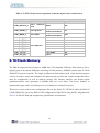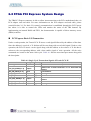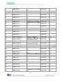
1
1 CONTENTS CHAPTER 1 OVERVIEW ................................................................................................................................. 3 1.1 GENERAL DESCRIPTION ..................................................................................................................................... 3 1.2 KEY FEATURES .................................................................................................................................................. 4 1.3 BOARD OVERVIEW ............................................................................................................................................. 5 1.4 BLOCK DIAGRAM .............................................................................................................................................. 6 CHAPTER 2 USING THE TR4 BOARD.......................................................................................................... 11 2.1 CONFIGURATION OPTIONS ................................................................................................................................. 11 2.2 SETUP ELEMENTS .............................................................................................................................................18 2.3 STATUS ELEMENTS ............................................................................................................................................19 2.4 GENERAL USER INPUT/OUTPUT .........................................................................................................................20 2.5 HIGH-SPEED MEZZANINE CARDS.......................................................................................................................22 2.6 GPIO EXPANSION HEADERS ..............................................................................................................................34 2.7 DDR3 SO-DIMM.............................................................................................................................................38 2.8 CLOCK CIRCUITRY ............................................................................................................................................42 2.9 PCI EXPRESS ....................................................................................................................................................45 2.10 FLASH MEMORY .............................................................................................................................................49 2.11 SSRAM MEMORY ...........................................................................................................................................52 2.12 TEMPERATURE SENSOR AND FAN .....................................................................................................................53 2.13 POWER ...........................................................................................................................................................54 2.14 SECURITY .......................................................................................................................................................54 CHAPTER 3 CONTROL PANEL .....................................................................................................................55 3.1 CONTROL PANEL SETUP ....................................................................................................................................55 3.2 CONTROLLING THE LEDS ..................................................................................................................................59 3.3 SWITCHES AND PUSH-BUTTONS .........................................................................................................................60 3.4 MEMORY CONTROLLER .....................................................................................................................................61 3.5 TEMPERATURE MONITOR ..................................................................................................................................64 3.6 PLL .................................................................................................................................................................65 3.7 HSMC .............................................................................................................................................................66 3.8 FAN ..................................................................................................................................................................67 3.9 INFORMATION ...................................................................................................................................................68 1 CHAPTER 4 TR4 SYSTEM BUILDER............................................................................................................70 4.1 INTRODUCTION .................................................................................................................................................70 4.2 GENERAL DESIGN FLOW ...................................................................................................................................70 4.3 USING TR4 SYSTEM BUILDER ...........................................................................................................................71 CHAPTER 5 EXAMPLES OF ADVANCED DEMONSTRATION....................................................................82 5.1 BREATHING LEDS.............................................................................................................................................82 5.2 EXTERNAL CLOCK GENERATOR .........................................................................................................................83 5.3 HIGH SPEED MEZZANINE CARD (HSMC) ...........................................................................................................89 5.4 DDR3 SDRAM (1GB)......................................................................................................................................91 5.5 DDR3 SDRAM (4GB)......................................................................................................................................94 CHAPTER 6 PCI EXPRESS REFERENCE DESIGN....................................................................................98 6.1 PCI EXPRESS SYSTEM INFRASTRUCTURE ...........................................................................................................98 6.2 FPGA PCI EXPRESS SYSTEM DESIGN ................................................................................................................99 6.3 PC PCI EXPRESS SYSTEM DESIGN ................................................................................................................... 103 6.4 PCIE FUNDAMENTAL COMMUNICATION ........................................................................................................... 112 6.5 IMAGE PROCESSING APPLICATION .................................................................................................................... 117 CHAPTER 7 APPENDIX A: HSMC PIN ASSIGNMENT ............................................................................... 123 ADDITIONAL INFORMATION................................................................................................................................. 1 2 Chapter 1 Overview This chapter provides an overview of the TR4 Development Board and details the components and features of the board. 1.1 General Description The TR4 Development Board provides the ideal hardware platform for system designs that demand high-performance, serial connectivity, and advanced memory interfacing. Developed specifically to address the rapidly evolving requirements in many end markets for greater bandwidth, improved jitter performance, and lower power consumption, the TR4 is powered by the Stratix® IV GX device and supported by industry-standard peripherals, connectors and interfaces that offer a rich set of features that is suitable for a wide range of compute-intensive applications. The advantages of the Stratix® IV GX FPGA platform with integrated transceivers have allowed the TR4 to be fully compliant with version 2.0 of the PCI Express standard. This will accelerate mainstream development of PCI Express-based applications and enable customers to deploy designs for a broad range of high-speed connectivity applications. The TR4 is supported by multiple reference designs and six High-Speed Mezzanine Card (HSMC) connectors that allow scaling and customization with mezzanine daughter cards. For large-scale ASIC prototype development, multiple TR4s can be stacked together to create an easily-customizable multi-FPGA system. 3 1.2 Key Features Featured Device o Altera Stratix® IV GX FPGA (EP4SGX230C2/EP4SGX530C2) Configuration and Set-up Elements o Built-in USB Blaster circuit for programming o Fast passive parallel (FPP) configuration via MAX II CPLD and FLASH Components and Interfaces o Six HSMC connectors (two with transceiver support) o Two 40-pin GPIO expansion headers (shares pins with HSMC Port C) o Two external PCI Express 2.0 (x4 lane) connectors Memory o DDR3 SO-DIMM socket (4GB Max) o 64MB FLASH o 2MB SSRAM General User Input/Output: o Four LEDs o Four push-buttons o Four slide switches Clock system o On-board 50MHz oscillator o o o o Three on-board programmable PLL timing chips SMA connector pair for differential clock input SMA connector pair for differential clock output SMA connector for external clock input o SMA connector for clock output Other o Temperature sensor o FPGA cooling fan 4 1.3 Board Over view Figure 1-1 and Figure 1-2 show the top and bottom view of the TR4 board. It depicts the layout of the board and indicates the location of the connectors and key components. Users can refer to these figures for relative location when the connectors and key components are introduced in the following chapters. Figure 1-1 TR4 Board View (Top) 5 Figure 1-2 TR4 Board View (Bottom) 1.4 Block Diagram Figure 1-3 shows the block diagram of the TR4 board. To provide maximum flexibility for the users, all key components are connected with the Stratix IV GX FPGA device, allowing the users to implement any system design. 6 Figure 1-3 TR4 Block Diagram Below is more detailed information regarding the blocks in Figure 1-3. Stratix IV GX FPGA EP4SGX230C2 o 228,000 logic elements (LEs) o 17,133K total memory Kb o 1,288 18x18-bit multipliers blocks o 2 PCI Express hard IP blocks o 744 user I/Os o 8 phase locked loops (PLLs) 7 EP4SGX530C2 o 531,200 logic elements (LEs) o o o o o 27,376K total memory Kb 1,024 18x18-bit multipliers blocks 4 PCI Express hard IP blocks 744 user I/Os 8 phase locked loops (PLLs) Configuration Device and USB Blaster Circuit MAXII CPLD EPM2210 System Controller and Fast Passive Parallel (FPP) configuration On-board USB Blaster for use with the Quartus II Programmer Programmable PLL timing chip configured via MAX II CPLD Supports JTAG mode Memory Devices 64MB Flash (32M x16) with a 16-bit data bus 2MB SSRAM (512K x 32) DDR3 SO-DIMM Socket Up to 4GB capacity Maximum memory clock rate at 533MHz Theoretical bandwidth up to 68Gbps LEDs 4 user-controllable LEDs Active-low Push-buttons 8 4 user-defined inputs Active-low Slide Switches 4 slide switches for user-defined inputs Logic low for DOWN position; Logic high for UP position On-Board Clocking Circuitry 50MHz oscillator SMA connector pair for differential clock inputs SMA connector pair for differential clock outputs SMA connector for external clock input SMA connector for clock output Two PCI Express x4 Edge Connectors Support connection speed of Gen1 at 2.5Gbps/lane to Gen2 at 5.0Gbps/lane Support downstream mode Six High Speed Mezzanine Card (HSMC) Connectors Two HSMC ports include 16 pairs of CDR-based transceivers at data rates of up to 6.5Gbps 52 true LVDS transmitter channels and 54 true LVDS receiver channels at data rate up to 1.6Gbps, 16 emulated LVDS transmitter channels and 14 emulated LVDS receiver channels at data rate up to 1.1Gbps Configurable I/O standards - 1.5V, 1.8V, 2.5V, 3.0V Two 40-pin GPIO Expansion Headers 72 FPGA I/O pins; 4 power and ground lines 9 Shares pins with HSMC Port C Configurable I/O standards: 1.5V, 1.8V, 2.5V, 3.0V Power Standalone DC 19V input Other Temperature Sensor Cooling Fan 10 Chapter 2 Using the TR4 Board This chapter gives instructions for using the TR4 board and its components. It is strongly recommended that users read the TR4 Getting Started Guide.pdf before operating the TR4 board. The document is located in the Usermanual folder on the TR4 System CD. The contents of the document include the following: Introduction to the TR4 Development Board TR4 Development Kit Contents Key Features Before You Begin Software Installation Development Board Setup Programming the Stratix IV GX Device Programming through Flash 2.1 Configuration Options JTAG FPGA Programming with USB-Blaster The USB-blaster is implemented on the TR4 board to provide a JTAG configuration through the on-board USB-to-JTAG configuration logic through the type-B USB connector, an FTDI USB 2.0 PHY device, and an Altera MAX II CPLD. For this programming mode, configuration data will be lost when the power is turned off. 11 To download a configuration bit stream into the Stratix IV GX FPGA, perform the following steps: Make sure that power is provided to the TR4 board. Open JP7 to bypass the JTAG interface of the HSMC if it won’t be used. Connect the USB cable supplied directly to the USB Blaster port of the TR4 board (see Figure 2-1). The FPGA can now be programmed in the Quartus II Programmer by selecting a configuration bit stream file with the .sof filename extension. If users need to use the JTAG interface on HSMC, please refer to Section 2.2 for detailed HSMC JTAG switch settings. Figure 2-1 JTAG Configuration Scheme JTAG FPGA Programming with External Blaster The TR4 board supports JTAG programming over external blaster via J2. To use this interface, users need to solder a 2x5 pin connector (2.54mm pitch) to J2. Make sure JP7 is open to bypass the JTAG interface of HSMC. Flash Programming The TR4 development board contains a common Flash interface (CFI) memory to meet the demands for larger FPGA configurations. The Parallel Flash Loader (PFL) feature in MAX II devices provides an efficient method to program CFI flash memory devices through the JTAG interface and the logic to control configuration from the flash memory device to the Stratix IV GX FPGA. Figure 2-2 depicts the connection setup between the CFI flash memory, Max II CPLD, and Stratix IV GX. 12 Figure 2-2 Flash Programming Scheme Programming Flash Memory using Batch File The TR4 provides a batch file (program_Flash.bat) to limit the steps that are taken when users program the flash memory on the TR4. Software Requirements: Quartus II 11.1 or later Nios II IDE 11.1 or later Program_Flash folder contents: Program_Flash.bat Program_Flash.pl Program_Flash.sh tr4_default_flash_loader.sof boot_loader_cfi.srec 13 Before you use the program_Flash.bat batch file to program the flash memory, make sure the TR4 is turned on and USB cable is connected to the USB blaster port (J4). In addition, place the .sof and .elf file you wish to program/convert in the Program_Flash directory. Programming Flash Memory with .sof using Program_Flash.bat 1. Launch the program_Flash.bat batch file from the directory (\demonstrations\TR4_<Stratix device>\ TR4_Default_Flash_Loaderr\Program_Flash) of the TR4 system CD-ROM. 2. The Flash program tool shows the menu options. Figure 2-3 Flash Program Tools 3. Select option 2. 14 Figure 2-4 Option 2 4. Enter the .sof file name to be programmed onto the flash memory. Figure 2-5 Enter .sof Name to Program 15 5. The following lines will appear during Flash programming: ‘Extracting Option bits SREC’, ‘Extracting FPGA Image SREC’, and ‘Deleting intermediate files’. If these lines don’t appear on the windows command, programming on the flash memory is not successfully set up. Please make sure Quartus II 11.1 and Nios II 11.1 IDE or later is used. Figure 2-6 Loading .sof File 6. Erasing Flash. 16 Figure 2-7 Erasing Flash 7. Programming Flash. Figure 2-8 Programming Flash 8. Programming complete. 17 Figure 2-9 Programming Flash complete 2.2 Setup Elements JTAG Control DIP Switch The TR4 supports individual JTAG interfaces on each HSMC connector. This feature allows users to extend the JTAG chain to daughter cards or additional TR4s. Before using this interface, JP7 needs to be shorted to enable the JTAG interface on all the HSMC connectors. The JTAG signals on each HSMC connector can be removed or included in the active JTAG chain via DIP switches. Table 2-1 lists the position of the DIP switches and their associated interfaces. Note that if the JTAG interface on HSMC connector is enabled, make sure that the active JTAG chain must be a closed loop or the FPGA may not be detected. Section 2.5 will give an example on how to extend the JTAG interface to a daughter card. Also, a document named Using_Mult-TR4_system.pdf in TR4 system CD shows how to connect the JTAG interface on two stacked TR4 boards. 18 Table 2-1 JTAG Control Components position 1 position 2 SW4 position 3 position 4 position 1 position 2 SW5 position 3 position 4 position 1 SW6 position 2 Name HSMCA_TOP HSMCB_TOP HSMCC_TOP HSMCD_TOP HSMCA_BOT HSMCB_BOT HSMCC_BOT HSMCD_BOT HSMCE_TOP HSMCF_TOP Description ON: HSMA TOP in-chain ON: HSMB TOP in-chain ON: HSMC TOP in-chain ON: HSMD TOP in-chain ON: HSMA BOT in-chain ON: HSMB BOT in-chain ON: HSMC BOT in-chain ON: HSMD BOT in-chain ON: HSME TOP in-chain ON: HSMF TOP in-chain OFF: Bypass HSMA TOP OFF: Bypass HSMB TOP OFF: Bypass HSMC TOP OFF: Bypass HSMD TOP OFF: Bypass HSMA BOT OFF: Bypass HSMB BOT OFF: Bypass HSMC BOT OFF: Bypass HSMD BOT OFF: Bypass HSME TOP OFF: Bypass HSMF TOP Default OFF OFF OFF OFF OFF OFF OFF OFF OFF OFF 2.3 Status Elements The TR4 includes status LEDs. Please refer Table 2-2 for the status of the LED indicator. Table 2-2 LED Indicators Board Reference LED name D13 HSMC Port E present D14 HSMC Port D present D15 HSMC Port A present D20 HSMC Port C Present D27 HSMC Port B Present D28 HSMC Port F Present D16 USB Blaster Circuit Description These LEDs are lit when HSMC Port A/B/C/D/E/F have a board or cable plugged-in such that pin 160 becomes grounded. This LED is lit when the USB blaster circuit transmits or receives data. 19 D17 MAX_LOAD D18 MAX_ERROR D19 MAX_CONF_DONEn This LED is lit when the FPGA is successfully configured. D33 19V POWER This LED is lit after the 19V adapter is plugged in D1~D12 This LED is lit when the FPGA is being actively configured. This LED is lit when the MAX II CPLD EPM2210 System Controller fails to configure the FPGA. HSMC VCCIO_LED These LEDs indicate the I/O standard of the HSMC ports (see Table 2-12) 2.4 General User Input/Output Push-buttons The TR4 includes six push-buttons that allow you to interact with the Stratix IV GX FPGA. Each of these buttons is debounced using a Schmitt Trigger circuit, as indicated in Figure 2-10. Each push-button provides a high logic level or a low logic level when it is not pressed or pressed, respectively (active-low). Table 2-3 lists the board references, signal names and their corresponding Stratix IV GX device pin numbers. Figure 2-10 Push-button Debouncing Table 2-3 Push-button Pin Assignments, Schematic Signal Names, and Functions Name Locate Description I/O Standard Stratix IV GX Pin Number PB3 BUTTON3 Low when pushed 1.5V PIN_P20 PB4 BUTTON2 (Active-low) 1.5V PIN_A19 PB5 BUTTON1 1.5V PIN_M19 20 PB6 BUTTON0 1.5V PIN_L19 The MAX_RSTN push-button is used to reset the MAX II EPM2210 CPLD. The Config push-button can configure default code to FPGA. Table 2–4 lists the board references, signal names and their corresponding Stratix IV GX device pin numbers. Table 2-4 Push-button Pin Assignments, Schematic Signal Names, and Functions Name Locate Description I/O EPM2210 Pin Number Standard PB1 MAX_RSTn MAX II reset 3.3V-VTTL PIN_M9 PB2 CONFIG FPGA reconfig 3.3V-VTTL PIN_D12 Slide Switches There are four slide switches on the TR4 to provide additional FPGA input control. Each switch is connected directly to a pin of the Stratix IV GX FPGA. When a slide switch is in the DOWN position or the UP position, it provides a low logic level or a high logic level (VCCIO_HSMF or VCCIO_HSMA) to the FPGA, respectively. Table 2–5 lists the board references, signal names and their corresponding Stratix IV GX device pin numbers. Table 2-5 Slide Switches Pin Assignments, Schematic Signal Names, and Functions Name Locate Description I/O Standard Stratix IV GX Pin Number SW0 SLIDE SW Provides high VCCIO_HSMF PIN_AH18 SW1 SLIDE SW logic level VCCIO_HSMF PIN_AH19 SW2 SLIDE SW when in the UP VCCIO_HSMA PIN_D6 SW3 SLIDE SW position VCCIO_HSMA PIN_C6 LEDs The TR4 consists of 4 user-controllable LEDs to allow status and debugging signals to be driven to the LEDs from the designs loaded into the Stratix IV GX device. Each LED is driven directly by the Stratix IV GX FPGA. The LED is turned on or off when the associated pins are driven to a low or high logic level, respectively (active-low). A list of the pin names on the FPGA that are connected to the LEDs is given in Table 2-6. 21 Table 2-6 User LEDs Pin Assignments, Schematic Signal Names, and Functions Name Description Description I/O Standard Stratix IV GX Pin Number D27 LED0 LEDs turn on when 1.5V PIN_B19 D28 LED1 output is logic low 1.5V PIN_A18 D29 LED2 (Active-low) 1.5V PIN_D19 D30 LED3 1.5V PIN_C19 2.5 High-Speed Mezzanine Cards The High Speed Mezzanine Card (HSMC) interface provides a mechanism to extend the peripheral-set of an FPGA host board by means of add-on daughter cards, which can address today’s high speed signaling requirements as well as low-speed device interface support. The HSMC interfaces support JTAG, clock outputs and inputs, high-speed serial I/O (transceivers), and single-ended or differential signaling. The detailed specifications of the HSMC connectors are described below: 6 HSMC Connector Groups There are ten HSMC connectors on the TR4 board are divided into 6 groups: HSMC A, HSMC B, HSMC C, HSMC D, HSMC E, and HSMC F. Each group has a male and female HSMC port on the top and bottom side of the TR4 board except HSMC E and HSMC F. In addition, both the male and female HSMC connector share the same I/O pins besides JTAG interface and high-speed serial I/O (transceivers). Caution: DO NOT connect HSMC daughter cards to the backside HSMC (male) connectors. Doing so will permanently damage the on-board FPGA. I/O Distribution The HSMC connector on the TR4 includes a total of 172 pins, including 121 signal pins (120 signal pins +1 PSNTn pin), 39 power pins, and 12 ground pins. Figure 2-11 shows the signal bank diagram of HSMC connector. Bank 1 also has dedicated JTAG, I2C bus, and clock signals. The main CMOS/LVDS interface signals, including LVDS/CMOS clocks, are found in banks 2 and 3. Both 12V and 3.3V power pins are also found in banks 2 and 3. 22 Figure 2-11 HSMC Signal Bank Diagram Due to the limitation of FPGA bank I/O distribution and dedicated clock in/out pin numbers, there are some differences between individual HSMC connectors, listed below: LVDS Interface On the TR4 board, only HSMC ports A, B, C and D support LVDS. Each HSMC port provides 18(1) LVDS channel transceivers. For LVDS transmitters, HSMC ports A and D support 18 true LVDS channels which can run up to 1.6Gbps. The LVDS transmitter on HSMC Port B and C contain true and emulated LVDS channels. The emulated LVDS channels use two single-ended output buffers and external resistors as shown in Figure 2-12. The associated I/O standard of these differential FPGA I/O pins in the Quartus II project should be set to LVDS_E_3R. Emulated LVDS I/O data rates can reach speeds up to 1.1Gbps. The factory default setting for the Rs resistor will be 0 ohm and the Rp resistor will not be 23 assembled for single-ended I/O standard applications. For emulated LVDS transmitters, please solder 120 and 170 ohm resistors onto the Rs and Rp positions, respectively. For the LVDS receivers, HSMC Port A/B/D support true LVDS receivers which can run at 1.6Gbps. Unlike HSMC ports A/D, not all the LVDS receivers in HSMC ports B/C support On-Chip termination (OCT). To use these I/Os as LVDS receivers, the user needs to solder a 100 ohm resistor for input termination as show in Figure 2-12. Table 2-7 gives the detailed numbers of true and emulated LVDS interfaces of each HSMC port. Also, it lists the numbers of LVDS receivers needed to assemble external input termination resistors on each HSMC ports. Table 2-8 shows all the external input differential resistors for LVDS receivers on HSMC Port B and C. The factory default setting is not installed. Finally, because HSMC Port C shares FPGA I/O pins with GPIO headers, so the LVDS performance can only support a data rate of up to 500Mbps. (1) Although the specifications of the HSMC connector defines signals D0~D3 as single-ended I/Os, D0 and D2 can be used as LVDS transmitters and D1 and D3 can be used as LVDS receivers on the TR4. Figure 2-12 Emulated LVDS Resistor Network between FPGA and HSMC Port 24 Figure 2-13 External On-Board Termination between FPGA and HSMC Port Table 2-7 LVDS Breakdown HSMA HSMB HSMC HSMD HSME HSMF True LVDS Transmitters 18 10 9 18 NA NA Emulated LVDS Transmitters 0 8 9 0 NA NA Supported with OCT 18 11 9 18 NA NA 0 7 9 0 NA NA Needed External Input Termination Resistors. Table 2-8 Distribution of the Differential Termination Resistors for HSMC Connector HSMC Differential Net Reference name of the differential termination resistor HSMB_RX_p[11] R333 HSMB_RX_p[12] R318 HSMB_RX_p[13] R312 HSMB_RX_p[14] R311 HSMB_RX_p[15] R303 HSMB_RX_p[16] R315 HSMB_D[1] R332 HSMC_RX_p[0] R314 HSMC_RX_p[1] R316 HSMC_RX_p[2] R330 HSMC_RX_p[3] R341 HSMC_RX_p[4] R329 HSMC_RX_p[5] R328 HSMC_RX_p[6] R309 25 HSMC_RX_p[7] R306 HSMC_D[1] R310 High-speed Serial I/O (transceiver) Interface There are 8 CDR transceiver channels located on the top side of HSMC ports A and E, respectively. Each CDR transceiver can run up to 6.5Gbps. Clock Interface Due to the limitation of the FPGA clock input pin numbers, not all the HSMC ports have same clock interface. Table 2-9 shows the FPGA clock input pin placement on each HSMC port. In addition, since FPGA dedicated clock input pins (CLK[1,3,8,10]), or corner PLL clocks don’t support On-Chip differential termination, please solder input termination resistors on R299 and R300, respectively, when using HSMC_CLKIN_p2/n2 and HSMA_CLKIN_p2/n2 as LVDS signals. Table 2-9 HSMC clock interface distribution FPGA Clock Input Pin Placement HSMC Clock in/out pin name HSMA HSMB HSMC HSMD HSME HSMF CLKIN0 I/O I/O I/O CLK1n I/O CLK5p CLKIN_p1 CLK9p I/O CLK2p CLK0p CLK11p CLK6p CLKIN_n1 CLK9n I/O CLK2n CLK0n CLK11n CLK6n CLKIN_p2 CLK8p I/O CLK3p I/O CLK10p CLK4p CLKIN_n2 CLK8n I/O CLK3n I/O CLK10n CLK4n I2C Interface The I2C bus on the HSMC connectors is separated into two groups. HSMC Port A, B, and C share the same I2C interface. HSMC ports D, E, and F share the other I2C bus. Table 2-10 lists the detailed distribution. 26 Table 2-10 HSMC I2C Group HSMC A/B/C I2C Schematic Signal Description I/O Standard Name Pin Number HSMC A/B/C I2C HSMB_SCL 2.5 V (1) AE16 2.5 V(1) AF16 clock signal HSMC A/B/C I2C HSMB_SDA Stratix IV GX data signal HSMC D/E/F I2C Schematic Signal Description I/O Standard Name Pin Number HSMC D/E/F I2C HSMD_SCL HSMD_SDA Stratix IV GX 1.5V(1) G21 1.5V(1) F21 clock signal HSMC D/E/F I2C data signal (1) The I2C I/O on the TR4 HSMC connector is defined with 3.3V. There is a level translator between FPGA and HSMC connector to translate FPGA 2.5V or 1.5V I/O to 3.3V. The signals above are also connected to the level translator. When these signals are used as general purpose I/O, the maximum data rate is 60Mbps. I/O through the Level Translator There is a pin named HSMD_OUT0 on HSMC Port D which is connected to an FPGA 1.5V I/O standard bank. To meet the I/O standard of adjustable specification, a level translator is used between the FPGA and HSMC Port D on this net. Thus, the maximum data rate of this pin is 60Mbps due to the limitations of the level translator. HSMC Port C Shared Bus with GPIO The HSMC Port C shares the same FPGA I/O pins with the GPIO expansion headers (JP9, JP10). Hence none of the combinations above are allowed to be used simultaneously. Power Supply 27 The TR4 board provides 12V DC and 3.3V DC power through HSMC ports. Table 2-11 indicates the maximum power consumption for all HSMC ports. Please note that this table shows the total max current limit for all six ports, not just for one. Also, the 12V DC and 3.3V DC power supplies from the HSMC ports have fuses for protection. Users who don’t need the power from the HSMC can remove these fuses to cut the power on connector. CAUTION. Before powering on the TR4 board with a daughter card, please check to see if there is a short circuit between the power pins and FPGA I/O. Table 2-11 Power Supply of the HSMC Supplied Voltage Max. Current Limit 12V 2A 3.3V 3A Adjustable I/O Standards The FPGA I/O standards of the HSMC ports can be adjusted by configuring the header position. Each port can be individually adjusted to 1.5V, 1.8V, 2.5V or 3.0V via jumpers on the top-right corner of TR4 board. Figure 2-14 depicts the position of the jumpers and their associated I/O standards. Users can use 2-pin jumpers to configure the I/O standard by choosing the associated positions on the header. Finally, there are LEDs on the top-right corner of TR4 board to indicate the I/O standard of each HSMC port, as shown in Table 2-12. For example, LEDs D11 and D12 will be turned on and off, respectively, when the I/O Standard of HSMC Port A is set to 2.5V. 28 Figure 2-14 HSMC I/O Configuration Header Table 2-12 HSMC IO Standard Indicators HSMA HSMB HSMC HSMD HSME HSMF D11 D12 D9 D10 D7 D8 D5 D6 D3 D4 D1 D2 1.5V OFF OFF OFF OFF OFF OFF OFF OFF OFF OFF OFF OFF 1.8V OFF ON OFF ON OFF ON OFF ON OFF ON OFF ON 2.5V ON OFF ON OFF ON OFF ON OFF ON OFF ON OFF 3.0V ON ON ON ON ON ON ON ON ON ON ON ON (1) Users who connect a daughter card onto the HSMC ports need to pay close attention to the I/O standard between TR4 HSMC connector pins and daughter card system. For example, if the I/O standard of HSMC pins on TR4 board is set to 1.8V, a daughter card with 3.3V or 2.5V I/O standard may not work properly on TR4 board due to I/O standard mismatch. When using custom or third-party HSMC daughter cards, make sure that all the pin locations are aligned to prevent shorts. Using THCB-HMF2 Adapter Card The purpose of the HSMC Height Extension Male to Female card (THCB-HMF2) included in the TR4 kit package is to increase the height of the HSMC (Port C and D) connector to avoid any obstruction that might take place as a HSMC daughter card is connected. The THCB-HMF2 adapter card can be connected to either ports of the HSMC connector shown in Figure 2-15. There are numerous adapter cards that are supported by the TR4, such as loopback and differential 29 transmission adapters. For more detailed information about these adapter cards, please refer to HSMC_adapter_card.pdf which can be found in TR4 system CD. Figure 2-15 Connection between HMF2 Adapter Card and HSMC JTAG Chain on HSMC The JTAG chain on the HSMC can be activated through the three 4-position DIP switches (SW4, SW5, and SW6). Table 2-1 in section 2.2 gives a detailed description of the positions of the DIP switches and their associated interfaces. The HSMC connectors on the top side of TR4 board are controlled by SW4 and SW6. SW5 is used to control the HSMC JTAG chain on the bottom-side of the TR4. Only when multiple TR4s are stacked should the boards use this switch. A document titled Using_Multi-TR4_system.pdf in the TR4 system CD will give an example to demonstrate how to set SW5 to connect JTAG chains together for multiple TR4 boards. Finally, before using the JTAG interface on HSMC connector, please short JP7 in order to enable the HSMC JTAG interface. 30 The following will describe how to configure the JTAG interface of HSMC connector on the top-side of the TR4. If there is no connection established on the HSMC connectors, the 4-position DIP switch (SW4 or SW6) should be set to ‘Off’, so the JTAG signals on the HSMC connectors are bypassed illustrated in Figure 2-16. Figure 2-16 JTAG Chain for a Standalone TR4 If the HSMC-based daughter card connected to the HSMC connector uses the JTAG interface, the 4-position DIP switch (SW4 or SW6) should be set to ‘On’ according to the HSMC port used. In this case, from Figure 2-17 HSMC Port D is used so position 4 of the SW4 switch is set to ‘On’. Similarly, if the JTAG interface isn’t used on the HSMC-based daughter card, position 4 of SW4 is set to ‘Off’, thus bypassing the JTAG signals as shown in Figure 2-18. 31 Figure 2-17 JTAG Chain for a Daughter Card (JTAG is used) Connected to HSMC Port D of the TR4 Figure 2-18 JTAG chain for a Daughter Card (JTAG not used) Connected to HSMC Port D of the TR4 32 Multi-FPGA High-Capacity Platforms through HSMC The TR4 offers a selection of two Stratix IV GX devices, EP4SGX230 and EPSGX530, which offer logic elements (LEs) up to 228,000 and 531,200, respectively, to provide the flexibility for users to select a suitable device. In situations where users’ design exceeds the capacity of the FPGA, the HSMC interface can be used to connect to other FPGA system boards creating a multi-FPGA scalable system. Users can stack two TR4s as shown in Figure 2-19. Another option is to use a Samtec high-speed cable to connect two TR4 boards (See Figure 2-20) to expand your system. For more information on how to use multi-TR4 systems, please refer to Using_Mult-TR4_system.pdf, which can be found on the TR4 System CD. Figure 2-19 Two Stacked TR4 Boards 33 Figure 2-20 Two TR4 Boards Connected via HSMC Cable 2.6 GPIO Expansion Header s The TR4 consists of two 40-pin expansion headers as shown in Figure 2-21. Each header has 36 I/O pins connected to the Stratix IV GX FPGA, with the other 4 pins providing 5V (VCC5) DC, 3.3V (VCC33) DC, and two GND pins. GPIO 0 and GPIO 1 share pins with HSMC Port C. The I/O standards of the GPIO headers are the same as HSMC Port C, which can be configured between 1.5, 1.8, 2.5 and 3.0V. 34 Figure 2-21 Pin Distribution of the GPIO Expansion Headers Finally, Figure 2-22 shows the connections between the GPIO expansion headers and Stratix IV GX. 35 Figure 2-22 Connection between the GPIO Expansion Headers and Stratix IV GX The information about mapping of the FPGA pin assignments to the GPIO0 and GPIO1 connectors, please refer Table 2-13 and Table 2-14. Table 2-13 GPIO Expansion Header (JP9) Pin Assignments, Schematic Signal Names, and Functions Board Reference Schematic Description (JP9) Signal Name 1 2 3 4 5 GPIO0_D0 GPIO0_D1 GPIO0_D2 GPIO0_D3 GPIO0_D4 GPIO Expansion 0 IO[0](Clock In) GPIO Expansion 0 IO[1] GPIO Expansion 0 IO[2](Clock In) GPIO Expansion 0 IO[3] GPIO Expansion 0 IO[4] 6 7 8 9 10 13 14 15 16 17 18 19 20 21 GPIO0_D5 GPIO0_D6 GPIO0_D7 GPIO0_D8 GPIO0_D9 GPIO0_D10 GPIO0_D11 GPIO0_D12 GPIO0_D13 GPIO0_D14 GPIO0_D15 GPIO0_D16 GPIO0_D17 GPIO0_D18 GPIO Expansion 0 IO[5] GPIO Expansion 0 IO[6] GPIO Expansion 0 IO[7] GPIO Expansion 0 IO[8] GPIO Expansion 0 IO[9] GPIO Expansion 0 IO[10] GPIO Expansion 0 IO[11] GPIO Expansion 0 IO[12] GPIO Expansion 0 IO[13] GPIO Expansion 0 IO[14] GPIO Expansion 0 IO[15] GPIO Expansion 0 IO[16] GPIO Expansion 0 IO[17] GPIO Expansion 0 IO[18] 36 I/O Standard Stratix IV GX Pin Number PIN_AF34 PIN_AG34 PIN_AE35 PIN_AG35 PIN_AC31 PIN_AH32 PIN_AC32 PIN_AH33 Depends on I/O PIN_AH34 Standard of HSMC PIN_AJ34 Port C PIN_AH35 PIN_AJ35 PIN_AK34 PIN_AL34 PIN_AK35 PIN_AL35 PIN_AM34 PIN_AN34 PIN_AM35 22 GPIO0_D19 GPIO Expansion 0 IO[19] PIN_AN35 23 24 GPIO0_D20 GPIO0_D21 GPIO Expansion 0 IO[20] GPIO Expansion 0 IO[21] PIN_AJ32 PIN_AJ26 25 26 27 28 31 32 33 34 35 36 37 38 39 40 GPIO0_D22 GPIO0_D23 GPIO0_D24 GPIO0_D25 GPIO0_D26 GPIO0_D27 GPIO0_D28 GPIO0_D29 GPIO0_D30 GPIO0_D31 GPIO0_D32 GPIO0_D33 GPIO0_D34 GPIO0_D35 GPIO Expansion 0 IO[22] GPIO Expansion 0 IO[23] GPIO Expansion 0 IO[24] GPIO Expansion 0 IO[25] GPIO Expansion 0 IO[26] GPIO Expansion 0 IO[27] GPIO Expansion 0 IO[28] GPIO Expansion 0 IO[29] GPIO Expansion 0 IO[30] GPIO Expansion 0 IO[31] GPIO Expansion 0 IO[32] GPIO Expansion 0 IO[33] GPIO Expansion 0 IO[34] GPIO Expansion 0 IO[35] PIN_AK33 PIN_AK26 PIN_AF25 PIN_AV29 Depends on I/O PIN_AG25 Standard of HSMC PIN_AW30 Port C PIN_AV32 PIN_AT28 PIN_AW32 PIN_AU28 PIN_AV28 PIN_AP28 PIN_AW29 PIN_AR28 Table 2-14 GPIO Expansion Header (JP10) Pin Assignments, Schematic Signal Names, and Functions Board Reference Schematic Description I/O Standard Stratix IV GX (JP10) Signal Name 1 2 3 4 5 6 7 8 9 10 13 14 15 GPIO1_D0 GPIO1_D1 GPIO1_D2 GPIO1_D3 GPIO1_D4 GPIO1_D5 GPIO1_D6 GPIO1_D7 GPIO1_D8 GPIO1_D9 GPIO1_D10 GPIO1_D11 GPIO1_D12 GPIO Expansion 1 IO[0] GPIO Expansion 1 IO[1] GPIO Expansion 1 IO[2] GPIO Expansion 1 IO[3] GPIO Expansion 1 IO[4] GPIO Expansion 1 IO[5] GPIO Expansion 1 IO[6] GPIO Expansion 1 IO[7] GPIO Expansion 1 IO[8] GPIO Expansion 1 IO[9] GPIO Expansion 1 IO[10] GPIO Expansion 1 IO[11] GPIO Expansion 1 IO[12] PIN_AB27 PIN_AE25 PIN_AB28 PIN_AD25 PIN_AP27 PIN_AU29 PIN_AN27 PIN_AT29 PIN_AL25 Depends on I/O PIN_AW33 Standard of HSMC PIN_AP26 Port C PIN_AW34 PIN_AW31 16 17 18 19 20 21 GPIO1_D13 GPIO1_D14 GPIO1_D15 GPIO1_D16 GPIO1_D17 GPIO1_D18 GPIO Expansion 1 IO[13] GPIO Expansion 1 IO[14] GPIO Expansion 1 IO[15] GPIO Expansion 1 IO[16] GPIO Expansion 1 IO[17] GPIO Expansion 1 IO[18] PIN_AH24 PIN_AV31 PIN_AG24 PIN_AL27 PIN_AW27 PIN_AH26 22 23 GPIO1_D19 GPIO1_D20 GPIO Expansion 1 IO[19] GPIO Expansion 1 IO[20] PIN_AW28 PIN_AK27 37 Pin Number 24 GPIO1_D21 GPIO Expansion 1 IO[21] PIN_AD30 25 26 GPIO1_D22 GPIO1_D23 GPIO Expansion 1 IO[22] GPIO Expansion 1 IO[23] PIN_AE24 PIN_AD31 27 28 31 32 33 34 35 36 37 38 39 40 GPIO1_D24 GPIO1_D25 GPIO1_D26 GPIO1_D27 GPIO1_D28 GPIO1_D29 GPIO1_D30 GPIO1_D31 GPIO1_D32 GPIO1_D33 GPIO1_D34 GPIO1_D35 GPIO Expansion 1 IO[24] GPIO Expansion 1 IO[25] GPIO Expansion 1 IO[26] GPIO Expansion 1 IO[27] GPIO Expansion 1 IO[28] GPIO Expansion 1 IO[29] GPIO Expansion 1 IO[30] GPIO Expansion 1 IO[31] GPIO Expansion 1 IO[32] GPIO Expansion 1 IO[33] GPIO Expansion 1 IO[34] GPIO Expansion 1 IO[35] PIN_AB30 PIN_AE30 PIN_AB31 PIN_AE31 Depends on I/O PIN_AG31 Standard of HSMC PIN_AE28 Port C PIN_AG32 PIN_AE29 PIN_AF29 PIN_AD28 PIN_AG30 PIN_AD29 2.7 DDR3 SO-DIMM One DDR3 SO-DIMM socket is provided as a flexible and efficient form-factor volatile memory for user applications. The DDR3 SODIMM socket is wired to support a maximum capacity of 4GB with a 64-bit data bus. Using differential DQS signaling for the DDR3 SDRAM interfaces, it is capable of running at up to 533MHz memory clock for a maximum theoretical bandwidth up to 68Gbps. Figure 2-23 shows the connections between the DDR3 SO-DIMM socket and Stratix IV GX device. The information about mapping of the FPGA pin assignments to the DDR3 SODIMM connectors, please refer to Table 2-15. Table 2-15 DDR3 SODIMM Pin Assignments, Schematic Signal Names, and Functions Schematic Stratix IV GX Signal Name Description I/O Standard Pin Number mem_addr [0] DDR3 ADDRess [0] SSTL-15 Class I PIN_N23 mem_addr [1] DDR3 ADDRess [1] SSTL-15 Class I PIN_C22 mem_addr [2] DDR3 ADDRess [2] SSTL-15 Class I PIN_M22 mem_addr [3] DDR3 ADDRess [3] SSTL-15 Class I PIN_D21 mem_addr [4] DDR3 ADDRess [4] SSTL-15 Class I PIN_P24 mem_addr [5] DDR3 ADDRess [5] SSTL-15 Class I PIN_A24 mem_addr [6] DDR3 ADDRess [6] SSTL-15 Class I PIN_M21 mem_addr [7] DDR3 ADDRess [7] SSTL-15 Class I PIN_D17 mem_addr [8] DDR3 ADDRess [8] SSTL-15 Class I PIN_A25 38 mem_addr [9] DDR3 ADDRess [9] SSTL-15 Class I PIN_N25 mem_addr [10] DDR3 ADDRess [10] SSTL-15 Class I PIN_C24 mem_addr [11] DDR3 ADDRess [11] SSTL-15 Class I PIN_N21 mem_addr [12] DDR3 ADDRess [12] SSTL-15 Class I PIN_M25 mem_addr [13] DDR3 ADDRess [13] SSTL-15 Class I PIN_K26 mem_addr [14] DDR3 ADDRess [14] SSTL-15 Class I PIN_F16 mem_addr [15] DDR3 ADDRess [15] SSTL-15 Class I PIN_R20 mem_ba[0] DDR3 Bank ADDRess [0] SSTL-15 Class I PIN_B26 mem_ba[1] DDR3 Bank ADDRess [1] SSTL-15 Class I PIN_A29 mem_ba[2] DDR3 Bank ADDRess [2] SSTL-15 Class I PIN_R24 DDR3 Column ADDRess mem_cas_n Strobe SSTL-15 Class I PIN_L26 mem_cke[0] Clock Enable pin 0 for DDR3 SSTL-15 Class I PIN_P25 mem_cke[1] Clock Enable pin 1 for DDR3 SSTL-15 Class I PIN_M16 mem_ck[0] Clock p0 for DDR3 Differential 1.5-V SSTL Class I PIN_K27 mem_ck[1] Clock p1 for DDR3 Differential 1.5-V SSTL Class I PIN_L25 mem_ck_n[0] Clock n0 for DDR3 Differential 1.5-V SSTL Class I PIN_J27 mem_ck_n[1] Clock n1 for DDR3 Differential 1.5-V SSTL Class I PIN_K28 mem_cs_n[0] DDR3 Chip Select [0] SSTL-15 Class I PIN_D23 mem_cs_n[1] DDR3 Chip Select [1] SSTL-15 Class I PIN_G28 mem_dm[0] DDR3 Data Mask [0] SSTL-15 Class I PIN_G16 mem_dm[1] DDR3 Data Mask [1] SSTL-15 Class I PIN_N16 mem_dm[2] DDR3 Data Mask [2] SSTL-15 Class I PIN_P23 mem_dm[3] DDR3 Data Mask [3] SSTL-15 Class I PIN_B29 mem_dm[4] DDR3 Data Mask [4] SSTL-15 Class I PIN_H28 mem_dm[5] DDR3 Data Mask [5] SSTL-15 Class I PIN_E17 mem_dm[6] DDR3 Data Mask [6] SSTL-15 Class I PIN_C26 mem_dm[7] DDR3 Data Mask [7] SSTL-15 Class I PIN_E23 mem_dq[0] DDR3 Data [0] SSTL-15 Class I PIN_G15 mem_dq[1] DDR3 Data [1] SSTL-15 Class I PIN_F15 mem_dq[2] DDR3 Data [2] SSTL-15 Class I PIN_C16 mem_dq[3] DDR3 Data [3] SSTL-15 Class I PIN_B16 mem_dq[4] DDR3 Data [4] SSTL-15 Class I PIN_G17 mem_dq[5] DDR3 Data [5] SSTL-15 Class I PIN_A16 mem_dq[6] DDR3 Data [6] SSTL-15 Class I PIN_D16 mem_dq[7] DDR3 Data [7] SSTL-15 Class I PIN_E16 39 mem_dq[8] DDR3 Data [8] SSTL-15 Class I PIN_N17 mem_dq[9] DDR3 Data [9] SSTL-15 Class I PIN_M17 mem_dq[10] DDR3 Data [10] SSTL-15 Class I PIN_K17 mem_dq[11] DDR3 Data [11] SSTL-15 Class I PIN_L16 mem_dq[12] DDR3 Data [12] SSTL-15 Class I PIN_P16 mem_dq[13] DDR3 Data [13] SSTL-15 Class I PIN_P17 mem_dq[14] DDR3 Data [14] SSTL-15 Class I PIN_J17 mem_dq[15] DDR3 Data [15] SSTL-15 Class I PIN_H17 mem_dq[16] DDR3 Data [16] SSTL-15 Class I PIN_N22 mem_dq[17] DDR3 Data [17] SSTL-15 Class I PIN_M23 mem_dq[18] DDR3 Data [18] SSTL-15 Class I PIN_J25 mem_dq[19] DDR3 Data [19] SSTL-15 Class I PIN_M24 mem_dq[20] DDR3 Data [20] SSTL-15 Class I PIN_R22 mem_dq[21] DDR3 Data [21] SSTL-15 Class I PIN_P22 mem_dq[22] DDR3 Data [22] SSTL-15 Class I PIN_K24 mem_dq[23] DDR3 Data [23] SSTL-15 Class I PIN_J24 mem_dq[24] DDR3 Data [24] SSTL-15 Class I PIN_A27 mem_dq[25] DDR3 Data [25] SSTL-15 Class I PIN_A28 mem_dq[26] DDR3 Data [26] SSTL-15 Class I PIN_C29 mem_dq[27] DDR3 Data [27] SSTL-15 Class I PIN_C30 mem_dq[28] DDR3 Data [28] SSTL-15 Class I PIN_C27 mem_dq[29] DDR3 Data [29] SSTL-15 Class I PIN_D27 mem_dq[30] DDR3 Data [30] SSTL-15 Class I PIN_A31 mem_dq[31] DDR3 Data [31] SSTL-15 Class I PIN_B31 mem_dq[32] DDR3 Data [32] SSTL-15 Class I PIN_G27 mem_dq[33] DDR3 Data [33] SSTL-15 Class I PIN_G29 mem_dq[34] DDR3 Data [34] SSTL-15 Class I PIN_F28 mem_dq[35] DDR3 Data [35] SSTL-15 Class I PIN_F27 mem_dq[36] DDR3 Data [36] SSTL-15 Class I PIN_E28 mem_dq[37] DDR3 Data [37] SSTL-15 Class I PIN_D28 mem_dq[38] DDR3 Data [38] SSTL-15 Class I PIN_H26 mem_dq[39] DDR3 Data [39] SSTL-15 Class I PIN_J26 mem_dq[40] DDR3 Data [40] SSTL-15 Class I PIN_F19 mem_dq[41] DDR3 Data [41] SSTL-15 Class I PIN_G19 mem_dq[42] DDR3 Data [42] SSTL-15 Class I PIN_F20 mem_dq[43] DDR3 Data [43] SSTL-15 Class I PIN_G20 40 mem_dq[44] DDR3 Data [44] SSTL-15 Class I PIN_C17 mem_dq[45] DDR3 Data [45] SSTL-15 Class I PIN_F17 mem_dq[46] DDR3 Data [46] SSTL-15 Class I PIN_C18 mem_dq[47] DDR3 Data [47] SSTL-15 Class I PIN_D18 mem_dq[48] DDR3 Data [48] SSTL-15 Class I PIN_D25 mem_dq[49] DDR3 Data [49] SSTL-15 Class I PIN_C25 mem_dq[50] DDR3 Data [50] SSTL-15 Class I PIN_G24 mem_dq[51] DDR3 Data [51] SSTL-15 Class I PIN_G25 mem_dq[52] DDR3 Data [52] SSTL-15 Class I PIN_B25 mem_dq[53] DDR3 Data [53] SSTL-15 Class I PIN_A26 mem_dq[54] DDR3 Data [54] SSTL-15 Class I PIN_D26 mem_dq[55] DDR3 Data [55] SSTL-15 Class I PIN_F24 mem_dq[56] DDR3 Data [56] SSTL-15 Class I PIN_F23 mem_dq[57] DDR3 Data [57] SSTL-15 Class I PIN_G23 mem_dq[58] DDR3 Data [58] SSTL-15 Class I PIN_J22 mem_dq[59] DDR3 Data [59] SSTL-15 Class I PIN_H22 mem_dq[60] DDR3 Data [60] SSTL-15 Class I PIN_K22 mem_dq[61] DDR3 Data [61] SSTL-15 Class I PIN_D22 mem_dq[62] DDR3 Data [62] SSTL-15 Class I PIN_G22 mem_dq[63] DDR3 Data [63] SSTL-15 Class I PIN_E22 mem_dqs[0] DDR3 Data Strobe p[0] Differential 1.5-V SSTL Class I PIN_D15 mem_dqs[1] DDR3 Data Strobe p[1] Differential 1.5-V SSTL Class I PIN_K16 mem_dqs[2] DDR3 Data Strobe p[2] Differential 1.5-V SSTL Class I PIN_L23 mem_dqs[3] DDR3 Data Strobe p[3] Differential 1.5-V SSTL Class I PIN_C28 mem_dqs[4] DDR3 Data Strobe p[4] Differential 1.5-V SSTL Class I PIN_E29 mem_dqs[5] DDR3 Data Strobe p[5] Differential 1.5-V SSTL Class I PIN_G18 mem_dqs[6] DDR3 Data Strobe p[6] Differential 1.5-V SSTL Class I PIN_F25 mem_dqs[7] DDR3 Data Strobe p[7] Differential 1.5-V SSTL Class I PIN_J23 mem_dqs_n[0] DDR3 Data Strobe n[0] Differential 1.5-V SSTL Class I PIN_C15 mem_dqs_n[1] DDR3 Data Strobe n[1] Differential 1.5-V SSTL Class I PIN_J16 mem_dqs_n[2] DDR3 Data Strobe n[2] Differential 1.5-V SSTL Class I PIN_K23 mem_dqs_n[3] DDR3 Data Strobe n[3] Differential 1.5-V SSTL Class I PIN_B28 mem_dqs_n[4] DDR3 Data Strobe n[4] Differential 1.5-V SSTL Class I PIN_D29 mem_dqs_n[5] DDR3 Data Strobe n[5] Differential 1.5-V SSTL Class I PIN_F18 mem_dqs_n[6] DDR3 Data Strobe n[6] Differential 1.5-V SSTL Class I PIN_E25 mem_dqs_n[7] DDR3 Data Strobe n[7] Differential 1.5-V SSTL Class I PIN_H23 41 mem_odt[0] DDR3 On-die Termination 0 SSTL-15 Class I PIN_F26 mem_odt[1] DDR3 On-die termination 1 SSTL-15 Class I PIN_G26 mem_ras_n DDR3 Row ADDRess Strobe SSTL-15 Class I PIN_D24 mem_we_n DDR3 Write Enable SSTL-15 Class I PIN_M27 mem_event_n DDR3 Temperature Event SSTL-15 Class I PIN_R18 mem_reset_n DDR3 Reset SSTL-15 Class I PIN_J18 mem_scl DDR3 I2C Serial Clock 1.5V PIN_H19 mem_sda DDR3 I2C Serial Data Bus 1.5V PIN_P18 Figure 2-23 Connection between DDR3 and Stratix IV GX FPGA 2.8 Clock Circuitr y Stratix IV GX FPGA Clock Inputs and Outputs The TR4 development board contains three types of clock inputs which include 26 global clock input pins, external PLL clock inputs and transceiver reference clock inputs. The clock input sources of the Stratix IV GX FPGA originate from on-board oscillators, a 50MHz, driven through the clock buffers as well as other interfaces including HSMC, GPIO expansion headers(share pins with HSMC Port C), and SMA connectors. The overall clock distribution of the TR4 is presented in Figure 2-24. 42 Figure 2-24 Clock Connections of the TR4 Note: (1) SMA_CLKOUT_p/N and some HSMC-A clock signals are connected to Bank 5C. If users use 43 SMA_CLKOUT_p/n ,please set HSMC-A I/O standard to 2.5V. (2) SMA_GXBCLK_p/n input HSMC-E and PCIE0’s Transceiver Bank GXBL. (3) PGM_GXBCLK_p1/n1input HSMC-A and PCIE1’s Transceiver Bank GXBR. (4) HSMD_OUT0 interface through a level shift, so the maximum speed is 60Mbps. The Stratix IV GX FPGA consists of 8 dedicated clock input pins and from those pins, 3 dedicated differential clock input listed in Table 2–19. In addition, there are a total of 8 PLLs available for the Stratix IV GX device. Table 2–19 Dedicated Clock Input Pins Dedicated Clock Input Pins OSC_50_BANK1 HSMD_CLKIN0 HSMC_CLKIN_p2 HSMC_CLKIN_n2 HSMA_CLKIN_p2 HSMA_CLKIN_n2 HSME_CLKIN_p2 HSME_CLKIN_n2 The dedicated clock input pins from the clock input multiplexer allow users to use any of these clocks as a source clock to drive the Stratix IV PLL circuit through the GCLK and RCLK networks. Alternatively, PLLs through the GCLK and RCLK networks or from dedicated connections on adjacent top/bottom and left/right PLLs can also drive the PLL circuit. The clock outputs of the Stratix IV GX FPGA are derived from various interfaces, notably the HSMC and the SMA connectors. Stratix IV GX FPGA Transceiver Clock Inputs The transceiver reference clock inputs for the serial protocols supported by the Stratix IV GX FPGA transceiver channels include the PCI Express (PIPE) and the SMA connectors. The TR4 uses three programmable low-jitter clock generators with default clock output of 100MHz and an I/O standard of LVDS that is non-configurable. The clock generators are programmed via Max II CPLD to generate the necessary clocks for the Stratix IV GX transceiver protocols and interfaces such as HSMC. The PCI Express (PIPE) transceiver reference clock is generated from the PCIe connector. 44 The clock frequency for the programmable clock generators can be specified by using the TR4 control panel, TR4 system builder, or the external clock generator demo provided. The associated pin assignments for clock buffer and SMA connectors to FPGA I/O pins are shown in Table 2–20. Table 2–20 Clock Inputs/Outputs Pin Assignments, Schematic Signal Names, and Functions Board Schematic Reference U49-4 Signal Name OSC_50_BANK1 U21-4 OSC_50_BANK3 U20-4 OSC_50_BANK4 U12-4 OSC_50_BANK7 U13-4 OSC_50_BANK8 U11-6 HSMA_REFCLK_p U11-5 HSMA_REFCLK_n U5-6 HSME_REFCLK_p U5-5 HSME_REFCLK_n J20 SMA_CLKOUT_p J19 SMA_CLKOUT_n J16 SMA_GXBCLK_p J17 SMA_GXBCLK_n J21 SMA_CLKIN Description Dedicated 50MHz clock input for bank 1C 50MHz clock input for bank 3C 50MHz clock input for bank 4C 50MHz clock input for bank 7C 50MHz clock input for bank 8C HSMC-A transceiver reference clock input HSMC-A transceiver reference clock input HSMC-E transceiver reference clock input HSMC-E transceiver reference clock input SMA differential clock output SMA differential clock output SMA transceiver reference clock input SMA transceiver reference clock input SMA clock input I/O Standard Stratix IV GX 2.5-V Pin Number AB34 2.5-V AW22 2.5-V AV19 1.5-V A21 1.5-V B23 LVDS AA2 LVDS AA1 LVDS AA38 LVDS AA39 2.5V or LVDS AC11 2.5V or LVDS AC10 LVDS J38 LVDS J39 2.5V AW19 2.9 PCI Express The TR4 development board features two PCIe Express downstream interfaces (x4 lane) which are designed to interface with a PC motherboard x4 slot via PCIe cable and PCIe adapter card. Utilizing 45 built-in transceivers on a Stratix IV GX device, it is able to provide a fully integrated PCI Express-compliant solution for multi-lane (x4) applications. With the PCI Express hard IP block incorporated in the Stratix IV GX device, it will allow users to implement simple and fast protocol, as well as saving logic resources for logic application. The PCI Express interface supports complete PCI Express Gen1 at 2.5Gbps/lane and Gen2 at 5.0Gbps/lane protocol stack solution compliant to PCI Express base specification 2.0 that includes PHY-MAC, Data Link, and transaction layer circuitry embedded in PCI Express hard IP blocks. To use PCIe interface, two external associated devices will be needed to establish link with PC. First, a PCIe half-height add-in host card with a PCIe x4 cable connector (See Figure 2-25) will be used to plug into the PCIe slot on a mother board. Then, a PCIe x4 cable (See Figure 2-26) will be used to connect TR4 board and PCIe add-in card as shown in Figure 2-27. These two associated devices are not included in TR4 kit. To purchase the PCIe add-in host card as well as the external cable, please contact Terasic sales team ([email protected]). Finally, section 6.3 and 6.4 demonstrate two examples on how to use the PCIe interface of TR4 board with a PC. Table 2-16 and Table 2-17 summarize the PCI Express pin assignments of the signal names relative to the Stratix IV GX FPGA. Figure 2-25 PCIe Adapter Card for Host Computer 46 Figure 2-26 PCIe External Cable Figure 2-27 PCIe Link Setup between TR4 and PC 47 Figure 2-28 PCI Express Pin Connection Table 2-16 PCIe0 Pin Assignments, Schematic Signal Names, and Functions PCIe0 4-Lane Downstream Name Description PCIE0_REFCLK_p PCIe0 reference clock PCIE0_PREST_n PCIe0 present PCIE0_WAKE_n PCIe0 wake PCIE0_TX_p[0] PCIE0_RX_p[0] PCIE0_TX_p[1] PCIE0_RX_p[1] PCIE0_TX_p[2] PCIE0_RX_p[2] PCIE0_TX_p[3] PCIE0_RX_p[3] PCIe0 data lane I/O Standard HCSL Depends on HSMC Port A I/O standard Depends on HSMC Port A I/O standard 1.4-V PCML 1.4-V PCML 1.4-V PCML 1.4-V PCML 1.4-V PCML 1.4-V PCML 1.4-V PCML 1.4-V PCML 48 Stratix IV GX Pin Number AN38 F8 AE10 AT36 AU38 AP36 AR38 AH36 AJ38 AF36 AG38 Table 2-17 PCIe1 Express Pin Assignments, Schematic Signal Names, and Functions PCIe1 4-Lane Downstream Name Description PCIE1_REFCLK_p PCIe1 clock PCIE1_PREST_n PCIe1 present PCIE1_WAKE_n PCIe1 wake PCIE1_TX_p[0] PCIE1_RX_p[0] PCIE1_TX_p[1] PCIE1_RX_p[1] PCIE1_TX_p[2] PCIE1_RX_p[2] PCIE1_TX_p[3] PCIE1_RX_p[3] reference PCIe1 data lane I/OStandard Stratix IV GX Pin Number HCSL AN2 Depends on HSMC Port A I/O standard Depends on HSMC Port A I/O standard 1.4-V PCML 1.4-V PCML 1.4-V PCML 1.4-V PCML 1.4-V PCML 1.4-V PCML 1.4-V PCML input G8 AE11 AT4 AU2 AP4 AR2 AH4 AJ2 AF4 AG2 2.10 Flash Memor y The TR4 development board features a 64MB Intel CFI-compliant NOR-type flash memory device which is part of the shared FMS Bus consisting of flash memory, SSRAM, and the Max II CPLD (EPM2210) System Controller. The single synchronous flash memory with 16-bit data bus supports 4-word, 8-word 16-word, and continuous-word burst mode provides non-volatile storage that can be used for configuration as well as software storage. The memory interface can sustain output synchronous-burst read operations at 40MHz with zero wait states. The device defaults to asynchronous page-mode read when power-up is initiated or returned from reset. This device is also used to store configuration files for the Stratix IV GX FPGA where the MAX II CPLD (EPM2210) can access flash for FPP configuration of the FPGA using the PFL Megafunction. Table 2-18 lists the flash pin assignments, signal names, and functions. 49 Figure 2-29 Connection between Flash, SSRAM, MAXII EPM2210 and the Stratix IV GX FPGA Table 2-18 Flash Memory Pin Assignments, Schematic Signal Names, and Functions Stratix IV GX Schematic Signal Name Description I/O Standard FSM_A1 FSM_A2 FSM_A3 FSM_A4 FSM_A5 Address bus Address bus Address bus Address bus Address bus 3.0-V PCI-X 3.0-V PCI-X 3.0-V PCI-X 3.0-V PCI-X 3.0-V PCI-X PIN_L31 PIN_F34 PIN_D35 PIN_D34 PIN_E34 FSM_A6 FSM_A7 FSM_A8 Address bus Address bus Address bus 3.0-V PCI-X 3.0-V PCI-X 3.0-V PCI-X PIN_C35 PIN_C34 PIN_F33 50 Pin Number FSM_A9 Address bus 3.0-V PCI-X PIN_G35 FSM_A10 FSM_A11 Address bus Address bus 3.0-V PCI-X 3.0-V PCI-X PIN_H35 PIN_J32 FSM_A12 FSM_A13 FSM_A14 FSM_A15 FSM_A16 FSM_A17 FSM_A18 FSM_A19 FSM_A20 FSM_A21 FSM_A22 FSM_A23 FSM_A24 FSM_A25 FSM_D0 FSM_D1 Address bus Address bus Address bus Address bus Address bus Address bus Address bus Address bus Address bus Address bus Address bus Address bus Address bus Address bus Data bus Data bus 3.0-V PCI-X 3.0-V PCI-X 3.0-V PCI-X 3.0-V PCI-X 3.0-V PCI-X 3.0-V PCI-X 3.0-V PCI-X 3.0-V PCI-X 3.0-V PCI-X 3.0-V PCI-X 3.0-V PCI-X 3.0-V PCI-X 3.0-V PCI-X 3.0-V PCI-X 3.0-V PCI-X 3.0-V PCI-X PIN_J33 PIN_K32 PIN_K31 PIN_AH17 PIN_AH16 PIN_AE17 PIN_AG16 PIN_H32 PIN_H34 PIN_G33 PIN_F35 PIN_N31 PIN_M31 PIN_M30 PIN_B32 PIN_C32 FSM_D2 FSM_D3 FSM_D4 FSM_D5 FSM_D6 FSM_D7 Data bus Data bus Data bus Data bus Data bus Data bus 3.0-V PCI-X 3.0-V PCI-X 3.0-V PCI-X 3.0-V PCI-X 3.0-V PCI-X 3.0-V PCI-X PIN_C31 PIN_F32 PIN_J30 PIN_K29 PIN_K30 PIN_L29 FSM_D8 FSM_D9 FSM_D10 FSM_D11 FSM_D12 FSM_D13 Data bus Data bus Data bus Data bus Data bus Data bus 3.0-V PCI-X 3.0-V PCI-X 3.0-V PCI-X 3.0-V PCI-X 3.0-V PCI-X 3.0-V PCI-X PIN_M29 PIN_N29 PIN_P29 PIN_T27 PIN_AM17 PIN_AL17 FSM_D14 FSM_D15 FLASH_CLK FLASH_RESET_n FLASH_CE_n FSM_OE_n FSM_WE_n FLASH_ADV_n FLASH_RDY_BSY_n FLASH_WP_n Data bus Data bus Clock Reset Chip Enable Output Enable Write Enable Address Valid Ready Write Protect 3.0-V PCI-X 3.0-V PCI-X 3.0-V PCI-X 3.0-V PCI-X 3.0-V PCI-X 3.0-V PCI-X 3.0-V PCI-X 3.0-V PCI-X 1.5 V 1.5 V PIN_AK16 PIN_AJ16 PIN_AU15 PIN_AV16 PIN_AP16 PIN_AT16 PIN_AL16 PIN_AT15 PIN_A23 PIN_A20 51 2.11 SSRAM Memor y The Synchronous Static Random Access Memory (SSRAM) device featured on the TR4 development board is part of the shared Flash-SSRAM-Max II (FSM) bus, which connects to Flash memory, SSRAM, and the MAX II CPLD (EEPM2210) System Controller. This device is a 2MB synchronously pipelined and high-speed, low-power synchronous static RAM designed to provide burstable, high-performance memory for communication and networking applications. Table 2-19 lists the SSRAM pin assignments and signal names relative to the Stratix IV GX device in terms of I/O setting. Table 2-19 SSRAM Memory Pin Assignments, Schematic Signal Names, and Functions Schematic Signal Name FSM_A2 FSM_A3 FSM_A4 FSM_A5 FSM_A6 FSM_A7 FSM_A8 FSM_A9 FSM_A10 FSM_A11 FSM_A12 FSM_A13 FSM_A14 FSM_A15 FSM_A16 FSM_A17 FSM_A18 FSM_A19 FSM_A20 FSM_A21 FSM_A22 FSM_D0 FSM_D1 FSM_D2 FSM_D3 FSM_D4 FSM_D5 FSM_D6 FSM_D7 Description I/O Standard Address bus A0 Address bus A1 Address bus A2 Address bus A3 Address bus A4 Address bus A5 Address bus A6 Address bus A7 Address bus A8 Address bus A9 Address bus A10 Address bus A11 Address bus A12 Address bus A13 Address bus A14 Address bus A15 Address bus A16 Address bus A17 Address bus A18 Address bus A19 Address bus A20 Data bus Data bus Data bus Data bus Data bus Data bus Data bus Data bus 3.0-V PCI-X 3.0-V PCI-X 3.0-V PCI-X 3.0-V PCI-X 3.0-V PCI-X 3.0-V PCI-X 3.0-V PCI-X 3.0-V PCI-X 3.0-V PCI-X 3.0-V PCI-X 3.0-V PCI-X 3.0-V PCI-X 3.0-V PCI-X 3.0-V PCI-X 3.0-V PCI-X 3.0-V PCI-X 3.0-V PCI-X 3.0-V PCI-X 3.0-V PCI-X 3.0-V PCI-X 3.0-V PCI-X 3.0-V PCI-X 3.0-V PCI-X 3.0-V PCI-X 3.0-V PCI-X 3.0-V PCI-X 3.0-V PCI-X 3.0-V PCI-X 3.0-V PCI-X 52 Stratix IV GX Pin Number PIN_F34 PIN_D35 PIN_D34 PIN_E34 PIN_C35 PIN_C34 PIN_F33 PIN_G35 PIN_H35 PIN_J32 PIN_J33 PIN_K32 PIN_K31 PIN_AH17 PIN_AH16 PIN_AE17 PIN_AG16 PIN_H32 PIN_H34 PIN_G33 PIN_F35 PIN_B32 PIN_C32 PIN_C31 PIN_F32 PIN_J30 PIN_K29 PIN_K30 PIN_L29 FSM_D8 FSM_D9 FSM_D10 FSM_D11 FSM_D12 FSM_D13 FSM_D14 FSM_D15 FSM_D16 FSM_D17 FSM_D18 FSM_D19 FSM_D20 FSM_D21 FSM_D22 FSM_D23 FSM_D24 FSM_D25 FSM_D26 FSM_D27 FSM_D28 FSM_D29 FSM_D30 FSM_D31 FSM_OE_n(OE_n) FSM_WE_n(BWE_n) SSRAM_ADSC_n SSRAM_ADSP_n SSRAM_ADV_n SSRAM_BE_n0 SSRAM_BE_n1 SSRAM_BE_n2 SSRAM_BE_n3 SSRAM_CE1_n SSRAM_CLK SSRAM_MODE SSRAM_GW_n SRAM_CE2 SSRAM_CE3_n SSRAM_ZZ Data bus Data bus Data bus Data bus Data bus Data bus Data bus Data bus Data bus Data bus Data bus Data bus Data bus Data bus Data bus Data bus Data bus Data bus Data bus Data bus Data bus Data bus Data bus Data bus Output Enable Byte Write Enable Address Status Controller Address Status Processor Synchronous Burst Address Advance Synchronous Byte Write Controls Synchronous Byte Write Controls Synchronous Byte Write Controls Synchronous Byte Write Controls Synchronous Chip Enable Synchronous Clock Burst Sequence Selection Synchronous Global Write Enable Synchronous Chip Enable Synchronous Chip Enable Power Sleep Mode 3.0-V PCI-X 3.0-V PCI-X 3.0-V PCI-X 3.0-V PCI-X 3.0-V PCI-X 3.0-V PCI-X 3.0-V PCI-X 3.0-V PCI-X 3.0-V PCI-X 3.0-V PCI-X 3.0-V PCI-X 3.0-V PCI-X 3.0-V PCI-X 3.0-V PCI-X 3.0-V PCI-X 3.0-V PCI-X 3.0-V PCI-X 3.0-V PCI-X 3.0-V PCI-X 3.0-V PCI-X 3.0-V PCI-X 3.0-V PCI-X 3.0-V PCI-X 3.0-V PCI-X 3.0-V PCI-X 3.0-V PCI-X 3.0-V PCI-X 3.0-V PCI-X 3.0-V PCI-X 3.0-V PCI-X 3.0-V PCI-X 3.0-V PCI-X 3.0-V PCI-X 3.0-V PCI-X 3.0-V PCI-X - PIN_M29 PIN_N29 PIN_P29 PIN_T27 PIN_AM17 PIN_AL17 PIN_AK16 PIN_AJ16 PIN_AK17 PIN_T28 PIN_R27 PIN_R28 PIN_R29 PIN_N30 PIN_N28 PIN_M28 PIN_H31 PIN_G31 PIN_D31 PIN_E31 PIN_F31 PIN_E32 PIN_C33 PIN_D33 PIN_AT16 PIN_AL16 PIN_AP17 PIN_AR17 PIN_AW16 PIN_AN16 PIN_AN17 PIN_AR16 PIN_AU16 PIN_AF17 PIN_AG17 - 2.12 Temperature Sensor and Fan The TR4 is equipped with a temperature sensor MAX1619, which provides temperature sensing and 53 over-temperature alerts. These functions are accomplished by connecting the temperature sensor to the internal temperature sensing diode of the Stratix IV GX device. The temperature status and alarm threshold registers of the temperature sensor can be programmed by a two-wire SMBus, which is connected to the Stratix IV GX FPGA. The 7-bit power-on-reset (POR) slave address for this sensor is ‘0011000b’. An optional 3-pin +12V header for fan control located on J10 of the TR4 board is intended to reduce the temperature of the FPGA. When the temperature of the FPGA device is over the threshold value set by the users, the fan will turn on automatically. The pin assignments for the associated interface are listed in Table 2-20. Table 2-20 Temperature Sensor Pin Assignments, Schematic Signal Names, and Functions Schematic Signal Name TEMP_SMCLK TEMP_SMDAT TEMP_OVERT_n TEMP_INT_n FAN_CTRL Description I/O Standard Stratix IV GX Pin Number SMBus clock SMBus data SMBus over-temperature alarm SMBus alert (interrupt) Fan control 2.5-V 2.5-V 2.5-V 2.5-V 1.5-V PIN_AR14 PIN_AP14 PIN_AK14 PIN_AH13 PIN_B17 2.13 Power The TR4 board features a standalone DC input rated at 19V.The DC voltage is stepped down to various power rails used by the components on the board and installed into the HSMC connectors. Power Switch The slide switch (SW7) is the board power switch for the DC power input. When the slide switch is in the ON position, the board is powered on. Alternatively when the switch is in the OFF position, the board is powered off. 2.14 Security The TR4 board features design security to protect your designs against unauthorized copying, reverse engineering, and tampering of your configuration files. For more information, please refer to Altera’s application note, “AN556: Using the Design Security Features in Altera FPGAs” 54 Chapter 3 Control Panel The TR4 board comes with a PC-based Control Panel that allows users to access various components onboard. The host computer communicates with the board via USB-Blaster port. The tool can be used to verify the functionality of components. This chapter presents some basic functions of the Control Panel, illustrates its structure in block diagram form, and finally describes its capabilities. 3.1 Control Panel Setup The Control Panel software utility is located in the directory “/Tools/TR4_ControlPanel” in the TR4 System CD. To execute the program, simply copy the whole folder to your host computer and launch the control panel by double clicking the TR4_ControlPanel.exe. CAUTION. Please make sure Quartus II and USB-Blaster Driver are installed before launching TR4 Control Panel. In addition, before the TR4 control panel is launched, it is imperative that the fan is installed on the Stratix IV GX device to prevent excessively high temperatures on the FPGA. To activate the Control Panel, perform the following steps: Make sure Quartus II and Nios II are installed successfully on your PC. Connect the supplied USB cable to the USB Blaster port and the supplied power cord to J4. Turn the power switch ON. Verify the connection on the USB blaster is available and not occupied or used between Quartus and TR4. Start the executable TR4_ControlPanel.exe on the host computer. Figure 3-1 will appear and the Control Panel starts to auto-detect the FPGA and download the .sof files. After the configuration file is programmed to the TR4 board, the FPGA device information will be displayed on the window. 55 Note. The Control Panel will occupy the USB port; users will not be able to download any configuration file into the FPGA before you exit the Control Panel program. Figure 3-1 Download .sof Files to the TR4 board The Control Panel is now ready, as shown in Figure 3-2. 56 Figure 3-2 TR4 Control Panel is Ready If the connection between TR4 board and USB-Blaster is not established, or the TR4 board is not powered on before running the TR4_ControlPanel.exe, the Control Panel will fail to detect the FPGA and a warning message window will pop up as shown in Figure 3-3. 57 Figure 3-3 The TR4 Control Panel Fails to Download .sof File The concept of the TR4 Control Panel is illustrated in Figure 3-4. The “Control Codes” which performs the control functions is implemented in the FPGA board. It communicates with the Control Panel window, which is active on the host computer, via the USB Blaster link. The graphical user interface is used to issue commands to the control codes. It handles all requests and performs data transfer between the computer and the TR4 board. 58 Figure 3-4 TR4 Control Panel Block Diagram The TR4 Control Panel can be used to illuminate the LEDs, monitoring buttons/switches status, read/write from various memory types, in addition to testing various components of the TR4 board. 3.2 Controlling the LEDs One of the functions of the Control Panel is to set up the status of the LEDs. The tab-window shown in Figure 3-5 indicates where you can directly turn all the LEDs on or off individually by selecting them and clicking “Light All” or “Unlight All”. 59 Figure 3-5 Controlling LEDs 3.3 Switches and Push-Buttons Choose the Button tab as shown in Figure 3-6. This function is designed to monitor status of switches and buttons from a graphical user interface in real-time. It can be used to verify the functionality of switches and buttons. 60 Figure 3-6 Monitoring Switches and Buttons 3.4 Memor y Controller The Control Panel can be used to write/read data to/from the DDR3 SO-DIMM/Flash/SSRAM memory on the TR4 board. We will describe how the DDR3 SO-DIMM is accessed. Click on the Memory tab to reach the tab-window shown in Figure 3-7. A 16-bit value can be written into the DDR3 SO-DIMM memory by three steps, namely specifying the address of the desired location, entering the hexadecimal data to be written, and pressing the Write button. Contents of the location can be read by pressing the Read button. Figure 3-8 depicts the result of writing the hexadecimal value 7EFF to location 0x100, followed by reading the same location. 61 The Sequential Write function of the Control Panel is used to write the contents of a file to the serial configuration device, as described below: Specify the starting address in the Address box. Specify the number of bytes to be written in the Length box. If the entire file is to be loaded, a check mark can be placed in the File Length box instead of giving the number of bytes. To initiate the writing of data, click on the Write a File to Memory button. When the Control Panel responds with the standard Windows dialog box asking for the source file, specify the desired file in the usual manner. The Sequential Read function is used to read the contents of the serial configuration device and place them into a file as follows: Specify the starting address in the Address box. Specify the number of bytes to be copied into a file in the Length box. If the entire contents of the serial configuration device are to be copied, then place a check mark in the Entire Memory box. Press Load Memory Content to a File button. When the Control Panel responds with the standard Windows dialog box ask for the destination file, users can specify the desired file in the usual manner. 62 Figure 3-7 Access DDR3 SO-DIMM Memory 63 Figure 3-8 Writing the Hexadecimal Value 7EFF to Location 0x100 3.5 Temperature Monitor Choose the Temperature tab to reach the window shown in Figure 3-9. This function is designed to control temperature sensor through the Control Panel. The temperatures of Stratix IV GX and TR4 board are shown on the right-hand side of the Control Panel. When the temperature of Stratix IV GX exceeds the maximum setting of ‘Over Temperature’ or ‘Alert’, a warning message will be shown on the Control Panel. Click “Read” button to get current settings for ‘Over temperature’ and ‘Alert’. Users can enter the maximum and minimum temperatures for ‘Over temperature’ or ‘Alert’ as required. Click the Write button to update the values entered. 64 Figure 3-9 Accessing the Temperature Sensor through Control Panel 3.6 PLL The PLL function is designed to configure the external programmable PLL on the TR4. There are 3 programmable clocks for the TR4 board that generates reference clocks for the following signals HSMA_REFCLK_p/n, HSMB_REFCLK_p/n, and PGM_GXBCLK_p1/n1. The clock frequency can be adjusted to 62.5, 75, 100, 125, 150, 156.25, 187.5, 200, 250, 312.5, and 625MHz. Choose the ‘PLL’ tab to reach the window shown in Figure 3-10. To set the desire clock frequency for the associated clock signal, click on ‘Set’. 65 Figure 3-10 Programmable External PLL Configured through Control Panel 3.7 HSMC Choose the HSMC tab to reach the window shown in Figure 3-11. This function is designed to verify the functionality of signals found on the HSMC connectors of ports A, B, C, D, E and F using a loopback approach. Before running the loopback verification HSMC test, select the desired HSMC connector to be tested. Follow the instruction noted under Loopback Installation section and click on ‘Verify’. Note the Control Panel HSMC loopback test does not test the transceiver signals on the HSMC interface. For HSMC transceiver loopback test, please refer to the demonstration section. CAUTION. Turn off the TR4 board before the HSMC loopback adapter is mounted to prevent any damage to the TR4 board. 66 Figure 3-11 HSMC Loopback Verification Test Performed under Control Panel 3.8 Fan Choose the Fan tab to reach the window shown in Figure 3-12. This function is designed to verify the functionality of the fan components and signals. Please make sure the fan is installed on the TR4 before running this function. 67 Figure 3-12 Fan Control of the TR4 3.9 Infor mation For more information, please click on the Information button in order to reach the window shown in Figure 3-13., Users can click “Terasic Web” button and “TR4_Web” button to reach the respective websites in order to learn more about the TR4 and Terasic Technologies. 68 Figure 3-13 Information Tab of TR4 Control Panel 69 Chapter 4 TR4 System Builder This chapter describes how users can create a custom design project on the TR4 board by using the included TR4 software tool – TR4 System Builder. 4.1 Introduction The TR4 System Builder is a Windows-based software utility, designed to assist users in creating a Quartus II project for the TR4 board within minutes. The generated Quartus II project files include: Quartus II Project File (.qpf) Quartus II Setting File (.qsf) Top-Level Design File (.v) External PLL Controller (.v) Synopsis Design Constraints file (.sdc) Pin Assignment Document (.htm) The TR4 System Builder not only can generate the files above, but can also provide error-checking rules to handle situations that are prone to errors. The common mistakes that users encounter are the following: Board damaged due to wrong pin/bank voltage assignments Board malfunction caused by wrong device connections or missing pin counts for connections Poor performance drop due to improper pin assignments 4.2 General Design Flow This section will introduce the general design flow to build a project for the TR4 board via the TR4 System Builder. The general design flow is illustrated in the Figure 4-1. 70 Users should launch TR4 System Builder and create a new project according to their design requirements. When users complete the settings, the TR4 System Builder will generate two major files which include a top-level design file (.v) and the Quartus II settings file (.qsf). The top-level design file contains a top-level Verilog wrapper for users to add their own design/logic. The Quartus II settings file contains information such as FPGA device type, top-level pin assignments, and I/O standards for each user-defined I/O pin. Finally, Quartus II programmer must be used to download SOF file to TR4 board using JTAG interface. Figure 4-1 General Design Flow 4.3 Using TR4 System Builder This section provides the detail procedures on how the TR4 System Builder is used. 71 Install and launch the TR4 System Builder The TR4 System Builder is located in the directory: "Tools\TR4_SystemBuilder" in the TR4 System CD. Users can copy the whole folder to a host computer without installing the utility. Before using the TR4 System Builder, execute the TR4_SystemBuilder.exe on the host computer as appears in Figure 4-2. Figure 4-2 TR4 System Builder Window Select Board Type and Input Project Name Select the target board type and input project name as show in Figure 4-3. Board Type: Select the appropriate FPGA device according to the TR4 board which includes the EP4SGX230 and EP4SGX530 devices. Project Name: Specify the project name as it is automatically assigned to the name of the 72 top-level design entity. Figure 4-3 TR4 Board Type and Project Name System Configuration Under System Configuration, users are given the flexibility of enabling their choice of components on the TR4 as shown in Figure 4-4. Each component of the TR4 is listed where users can enable or disable a component according to their design by simply marking a check or removing the check in the field provided. If the component is enabled, the TR4 System Builder will automatically generate the associated pin assignments including the pin name, pin location, pin direction, and I/O standards. Note. The pin assignments for some components for e.g. DDR3 require associated controller codes in the Quartus II project otherwise Quartus II will result in compilation errors. Therefore, do not select them if they are not necessary in your design. 73 Figure 4-4 System Configuration Group Programmable PLL There are three external programmable PLLs on-board that provide reference clocks for the following signals HSMA_REFCLK, HSME_REFLCLK and PGM_GXBCLK. To use these PLLs, users can select the desired frequency on the Programmable PLL group, as shown in Figure 4-5. As the Quartus II project is created, System Builder automatically generates the associated PLL configuration code according to users’ desired frequency in Verilog which facilitates users’ implementation as no additional control code is required to configure the PLLs. Note. If users need to dynamically change the frequency, they will need to modify the generated control code themselves. 74 Figure 4-5 External Programmable PLL HSMC Expansion Users can connect HSMC-interfaced daughter cards onto the HSMC ports located on the TR4 board shown in Figure 4-6. Select the daughter card you wish to add to your design under the appropriate HSMC connector where the daughter card is connected to. The System Builder will automatically generate the associated pin assignment including pin name, pin location, pin direction, and IO standard. If a customized daughter board is used, users can select “HSMC Default” followed by changing the pin name, pin direction, and IO standard according to the specification of the customized daughter board. If transceiver pins are not required on the daughter board, please remember to remove it, otherwise Quartus II will report errors. 75 Figure 4-6 HSMC Expansion Group The “Prefix Name” is an optional feature that denotes the pin name of the daughter card assigned in your design. Users may leave this field empty. Note. If the same HSMC daughter card is selected in both HSMC-A and HSMC-B expansion, a prefix name is required to avoid pin name duplication as shown in Figure 4-7, otherwise System Builder will prompt an error message. 76 Figure 4-7 Specify Prefix Name for HSMC Expansion Board Additionally, users can choose the “HSMC-C/GPIO” as either “HSMC” or “GPIO”, since the GPIO ports share pins with HSMC Port C as shown in Figure 4-8. 77 Figure 4-8 HSMC-C/GPIO share pins option After users select the “GPIO” option, a “GPIO Edit” button will appear. If this is clicked, a “GPIO Expansion” window will pop up for users to select a compatible Terasic daughter card. Once a daughter card selected, the JP4 header diagram in the upper left hand corner of the window, which configures HSMC Port C and GPIO I/O standards will adjust automatically to recommend a suitable I/O standard for the selected daughter card as shown in Figure 4-9. 78 Figure 4-9 GPIO option and I/O standard recommend Project Setting Management The TR4 System Builder also provides functions to restore a default setting, loading a setting, and saving users’ board configuration file shown in Figure 4-10. Users can save the current board configuration information into a .cfg file and load it to the TR4 System Builder. 79 Figure 4-10 Project Settings Project Generation When users press the Generate button, the TR4 System Builder will generate the corresponding Quartus II files and documents as listed in the Table 4-1 in the directory specified by the user. Table 4-1 No. Files Generated by TR4 System Builder Filename Description 1 <Project name>.v Top level Verilog file for Quartus II 2 EXT_PLL_CTRL.v External PLL configuration controller IP 3 4 5 <Project name>.qpf Quartus II Project File <Project name>.qsf Quartus II Setting File <Project name>.sdc Synopsis Design Constraints file for Quartus II 80 6 <Project name>.htm Pin Assignment Document Users can use Quartus II software to add custom logic into the project and compile the project to generate the SRAM Object File (.sof). In addition, External Programmable PLL Configuration Controller IP will be instantiated in the Quartus II top-level file as listed below: ext_pll_ctrl u_ext_pll_ctrl ( // system input .osc_50(OSC_50_BANK1), .rstn(rstn), // device 1 .clk1_set_wr(clk1_set_wr), .clk1_set_rd(), // device 2 .clk2_set_wr(clk2_set_wr), .clk2_set_rd(), // device 3 .clk3_set_wr(clk3_set_wr), .clk3_set_rd(), // setting trigger .conf_wr(conf_wr), .conf_rd(), // status // 1T 50MHz // 1T 50MHz .conf_ready(), // 2-wire interface .max_sclk(MAX2_I2C_SCL), .max_sdat(MAX2_I2C_SDA) ); If dynamic PLL configuration is required, users need to modify the code according to users’ desired PLL behavior. 81 Chapter 5 Examples of Advanced Demonstration This chapter introduces several advanced designs that demonstrate Stratix IV GX features using the TR4 board. The provided designs include the major features on board such as the HSMC connectors, PCIe, and DDR3. For each demonstration the Stratix IV GX FPGA configuration file is provided, as well as full source code in Verilog HDL. All of the associated files can be found in the demonstrations\tr4_<Stratix device> folder from the TR4 System CD. For each of demonstrations described in the following sections, we give the name of the project directory for its files, which are sub-directories of the demonstrations\tr4_<Stratix_device> folder. 5.1 Breathing LEDs This demonstration shows how to use the FPGA to control the luminance of the LEDs by means of dividing frequency. By dividing the frequency from 50 MHz to 1 Hz, you can see LED flash once per second. Design Tools Quartus II 11.1 Demonstration Source Code Project directory: Breathing_LEDs Bit stream used: Breathing_LEDs.sof Demonstration Batch File Demo Batch File Folder: Breathing_LEDs\ Demo_batch 82 The demo batch file includes following files: Batch File: Breathing_LEDs.bat FPGA Configuration File: Breathing_LEDs.sof Demonstration Setup Make sure Quartus II and Nios II are installed on your PC. Connect the USB Blaster cable to the TR4 board and host PC. Install the USB Blaster driver if necessary. Power on the TR4 board. Execute the demo batch file “Breathing_LEDs.bat” under the batch file folder, TR4_Breathing_LEDs\Demo_batch. Press BUTTON0 of the TR4 board to reset. The LEDs will pulse according to the set frequency. 5.2 Exter nal Clock Generator The External Clock Generator provides designers with 3 programmable clock generators via Texas Instruments chips (CDCM61001RHBT x 2, CDCM61004RHBT) with the ability to specify the clock frequency individually, as well as addressing the input reference clock for the Stratix IV GX transceivers. The programmable clock is controlled by a control bus connected to the MAX II EPM2210 device. This can reduce the Stratix IV GX I/O usage while enabling greater functionality on the FPGA device. The MAX II EPM2210 device is capable of storing the last entered clock settings at which in the event the board restarts, the last known clock settings are fully restored. In this demonstration, we illustrate how to utilize the clock generators IP to define the clock output using the serial bus. The programmable clock outputs generate clock signals HSMA_REFCLK_p/n (CDCM61001/01), PGM_GXBCLK_p1/n1 (CDCM61004), and HSME_REFCLK_p/n (CDCM61001/02) with adjustable output clock frequencies of 62.5, 75, 100, 125, 150, 156.25, 187.5, 200, 250, 312.5, and 625MHz. The I/O standard for the clock frequencies is set to LVDS which is not configurable. An overall block diagram of the external clock generator is shown below in Figure 5-1. 83 Figure 5-1 External Clock Generator Block Diagram The EXT_PLL_CTRL IP Port Description This section describes the operation for the EXT_PLL_CTRL instruction hardware port. Figure 5-2 shows the EXT_PLL_CTRL instruction block diagram connected to the MAX II EPM2210 device. The EXT_PLL_CTRL controller module is defined by a host device, the Stratix IV GX FPGA and a slave device, the MAX II EPM2210. Through the I2C bus interface, the EXT_PLL_CTRL controller is able to control the Max II device by specifying the desire clock outputs set by the user. By changing the IP parameters of the Terasic EXT_PLL_CTRL IP, the external clock output 84 frequency can be adjusted accordingly. Figure 5-2 EXT_PLL_CTRL Instruction Hardware Ports Table 5-1 lists the EXT_PLL_CTRL instruction ports Table 5-1 Port Name EXT_PLL_CTRL Instruction Ports Direction Description osc_50 rstn clk1_set_wr clk2_set_wr clk3_set_wr clk1_set_rd clk2_set_rd clk3_set_rd conf_wr input input System Clock (50MHz) Synchronous Reset (0: Module Reset, 1: Normal) input Setting Output Frequency Value output Read Back Output Frequency Value Input Start to Transfer Serial Data(postive edge) conf_rd Input conf_ready Output max_sclk max_sdat Output Inout Start to Read Serial Data (postive edge) Serial Data Transmission is Complete ( 0: Transmission in Progress, 1: Transmission Complete) Serial Clock to MAX II Serial Data to/from MAX II The EXT_PLL_CTRL IP Parameter Setting Users can refer to the following Table 5-2 to set the external clock generator for the output frequency. Table 5-2 clk1_set_wr/ clk2_set_wr/ EXT_PLL_CTRL Instruction Ports Output Frequency(MHz) 85 Description clk3_set_wr 4’b0001 4’b0010 x 62.5 4’b0011 4’b0100 4’b0101 4’b0110 75 100 125 150 4’b0111 4’b1000 156.23 187 4’b1001 4’b1010 4’b1011 4’b1100 Others 200 250 312.5 625 x Clock Generator Disable Setting External Clock Generator Setting Unchanged The EXT_PLL_CTRL IP Timing Diagram In this reference design the output frequency is set to 62.5, 75 and 100 MHz with the following timing diagrams illustrated below. When the ext_pll_ctrl IP receives the ‘conf_wr’ signal, the user needs to define (clk1_set_wr, clk2_set_wr and clk3_set_wr) to set the External Clock Generator. When the ext_pll_ctrl IP receives the ‘conf_rd’ signal, it will read the value back to clk1_set_rd, clk2_set_rd, and clk3_set_rd. Write Timing Waveform: As BUTTON0 (the trigger source defined by Terasic) is pressed, the 'conf_wr' signal is on the rising edge, serial data is transferred immediately with the 'conf_ready' signal in the transmission period starting at falling edge level as shown in Figure 5-3. As the transfer is completed, the ‘conf_ready’ signal returns back to original state at high-level. 86 Figure 5-3 Write Timing Waveform Read Timing Waveform: As BUTTON1 (the trigger source defined by Terasic) is pressed the 'conf_rd' signal is on the rising edge, the user settings are read back immediately once the 'conf_ready' signal is on the falling edge as shown in Figure 5-4. As the transfer is complete, the ‘conf_ready’ returns back to original state at high-level. 87 Figure 5-4 Read Timing Waveform Design Tools Quartus II 11.1 Demonstration Source Code Project directory: TR4_EXT_PLL Bit stream used: TR4_EXT_PLL.sof Demonstration Batch File Demo Batch File Folder: TR4_EXT_PLL\demo_batch The demo batch file folders include the following files: Batch File: TR4_EXT_PLL.bat FPGA Configuration File: TR4_EXT_PLL.sof Demonstration Setup Make sure Quartus II is installed on your PC. 88 Connect the USB Blaster cable to the TR4 board and host PC. Install the USB Blaster driver if necessary. Power on the TR4 board. Execute the demo batch file “TR4_EXT_PLL.bat” under the batch file folder, TR4_EXT_PLL\demo_batch Press BUTTON0 to configure the external PLL chips via MAX CPLD. 5.3 High Speed Mezzanine Card (HSMC) The HSMC loopback demonstration reference design observes the traffic flow with an HSMC loopback adapter which provides a quick way to implement your own design utilizing the transceiver signals situated on the HSMC interface. This design also helps you verify the transceiver signals functionality for ports A and E of the HSMC interface. A total of 8 transceiver pairs on the HSMC Port A and port E each are tested. HSMC Port A Loopback Test: Demonstration Source Code Quartus Project directory: TR4_HSMA_LOOPBACK_TEST FPGA Bit Stream: TR4_HSMA_LOOPBACK_TEST.sof Demonstration Setup Check that Quartus II and Nios II are installed on your PC. Insert the HSMC loopback adapter onto the HSMC Port A. Connect the USB Blaster cable to the TR4 board and host PC. Install the USB Blaster driver if necessary. Power on the TR4 board. Program the TR4 using the TR4_HSMA_LOOPBACK_TEST.sof through Quartus II programmer. Press BUTTON0 of the TR4 board to initiate the verification process. LED [3:0] will flash indicating the loopback test passed. HSMC Port E Loopback Test: 89 Demonstration Source Code Quartus Project directory: TR4_HSME_LOOPBACK_TEST FPGA Bit Stream: TR4_HSME_LOOPBACK_TEST.sof Demonstration Setup Check that Quartus II and Nios II are installed on your PC. Insert the HSMC loopback daughter card onto the HSMC Port E as shown in Figure 5-5. Connect the USB Blaster cable to the TR4 board and host PC. Install the USB Blaster driver if necessary. Power on the TR4 board. Program the TR4 using the TR4_HSME_LOOPBACK_TEST.sof through Quartus II programmer. Press BUTTON0 on the TR4 board to initiate the verification process LED [3:0] will flash once to indicate the loopback test passed. Figure 5-5 HSMC Loopback Design Setup 90 5.4 DDR3 SDRAM (1GB) Many applications use a high performance RAM, such as a DDR3 SDRAM to provide temporary storage. In this demonstration hardware and software designs are provided to illustrate how the DDR3 SDRAM SODIMM on the TR4 can be accessed. We describe how the Altera’s “DDR3 SDRAM Controller with UniPHY” IP is used to create a DDR3-SDRAM controller, and how the Nios II processor is used to read and write the SDRAM for hardware verification. The DDR3 SDRAM controller handles the complex aspects of using DDR3-SDRAM by initializing the memory devices, managing SDRAM banks, and keeping the devices refreshed at appropriate intervals. The required DDR3-SDRAM SODIMM module should be 1 GB DDR3-1066. System Block Diagram Figure 5-6 shows the system block diagram of this demonstration. The system requires a 50 MHz clock provided from the board. The DDR3 controller is configured as a 1GB DDR3-1066 controller. The DDR3 IP generates one 533.0 MHz clock as memory clock and one quarter-rate system clock 133.125 MHz for controllers, e.g. Nios II processor, accessing the SDRAM. In Qsys, Nios II and On-Chip Memory are designed running with the 133.125 MHz clock, and the other controllers are designed running with 50 MHz clock which is the external clock. The Nios II program itself is running in the on-chip memory. Figure 5-6 Block diagram of the DDR3 1G demonstration The system flow is controlled by a Nios II program. First, the Nios II program writes test patterns into the DDR3, filling it up to maximum capacity. Then, it calls a Nios II system function, 91 alt_dache_flush_all, to make sure all data has been written. Finally, it reads data from DDR3 for data verification. The program will show progress in JTAG-Terminal when writing/reading data to/from the DDR3. When the verification process is completed, the result is displayed in the JTAG-Terminal. Altera DDR3 SDRAM Controller with UniPHY To use the Altera DDR3 controller, users need to perform three major steps: 1). Create correct pin assignments for the DDR3. 2). Set up correct parameters in DDR3 controller dialog. 3). Execute TCL files, generated by DDR3 IP, under your Quartus II project. The following section describes some of the important issues in support of the DDR3 controller configuration. On the “PHY_Setting” tab, in order to achieve 533.0 MHz clock frequency, a reference clock frequency of 50 MHz should be used. If a different DDR3 SODIMM is used, the memory parameters should be modified according to the datasheet of the DDR3 SODIMM. Design Tools Quartus II 11.1 Nios II IDE 11.1 Demonstration Source Code Project directory: TR4_DDR3_UniPHY_1G_QSYS Bit stream used: TR4_DDR3_UniPHY_1G_QSYS.sof Nios II Workspace: TR4_DDR3_UniPHY_1G_QSYS\Software Demonstration Batch File Demo Batch File Folder: TR4_DDR3_UniPHY_1G_QSYS\demo_batch The demo batch file includes following files: Batch File: TR4_DDR3_UniPHY_1G_QSYS.bat, TR4_DDR3_UniPHY_1G_QSYS_bashrc FPGA Configuration File: TR4_DDR3_UniPHY_1G_QSYS.sof Nios II Program: TR4_DDR3_UniPHY_1G_QSYS.elf 92 Demonstration Setup Make sure Quartus II and Nios II are installed on your PC. Make sure DDR3-SDRAM SODIMM (1G) is inserted into your TR4 board, as shown in Figure 5-7. Connect the USB Blaster cable to the TR4 board and host PC. Install the USB Blaster driver if necessary. Power on the TR4 board. Execute the demo batch file “TR4_DDR3_UniPHY_1G_QSYS.bat” under the batch file folder, TR4_DDR3_UniPHY_1G_QSYS\demo_batch. After Nios II program is downloaded and executed successfully, a prompt message will be displayed in nios2-terminal. Press BUTTON3~BUTTON0 of the TR4 board to start the DDR3 verification process. Press BUTTON0 to continue the test and Ctrl+C to terminate the test The program will display the progress and result, as shown in Figure 5-8 Figure 5-7 Insert the DDR3-SDRAM SODIMM for the DDR3 1G Demonstration 93 Figure 5-8 Display Progress and Result for the DDR3 1G Demonstration 5.5 DDR3 SDRAM (4GB) This demonstration presents user a basic utilization of DDR3-SDRAM (4G) on TR4.It describes how the Altera’s “DDR3 SDRAM Controller with UniPHY” IP is used to create a DDR3-SDRAM controller, and modify the IP-generated example top to test the entire space of DDR3-SDRAM. This demonstration is a pure RTL project. The required DDR3-SDRAM SODIMM module should be exactly 4 GB of DDR3-1066. Function Block Diagram Figure 5-9 shows the function block diagram of this demonstration. The DDR3 controller is configured as a 4GB DDR3-1066 controller. The DDR3 IP generates one 533.0 MHz clock as memory clock and one half-rate system clock, 266.5 MHz, for the controller. 94 Figure 5-9 Block Diagram of the DDR3 4G Demonstration The project is based on the example top code which is generated by the DDR3 IP, and can be used to test the whole module after modifying the code. In the project, example driver will read out the data for a comparison after writing every 1KB pseudo-random data. The read compare module will buffer the write data, and then compare it with the data read back. If the right result is achieved, the address will be accumulated and the test will check the whole memory span of 4GB after finishing 4*1024*1024 loops. Altera DDR3 SDRAM Controller with UniPHY To use Altera DDR3 controller, users need to perform three major steps: 1). Create correct pin assignment for DDR3. 2). Setup correct parameters in DDR3 controller dialog. 3). Execute TCL files, generated by DDR3 IP, under your Quartus project. The following section describes some of the important issues in support of the DDR3 controller configuration. On the “PHY_Setting” tab, in order to achieve 533.0 MHz clock frequency, a reference clock frequency of 50 MHz should be used. Design Tools Quartus II 11.1 Demonstration Source Code 95 Project directory: TR4_DDR3_UniPHY_4G_RTL Bit stream used: TR4_DDR3_UniPHY_4G_RTL.sof Demonstration Batch File Demo Batch File Folder: TR4_DDR3_UniPHY_4G_RTL\demo_batch The demo batch file includes following files: Batch File: TR4_DDR3_UniPHY_4G_RTL.bat FPGA Configure File: TR4_DDR3_UniPHY_4G_RTL.sof Demonstration Setup Make sure Quartus II is installed on your PC. Make sure DDR3-SDRAM SODIMM (4 GB) is installed on your TR4 board, as shown in Figure 5-10. Connect the USB Blaster cable to the TR4 board and host PC. Install the USB Blaster driver if necessary. Power on the TR4 board. Execute the demo batch file “TR4_DDR3_UniPHY_4G_RTL.bat” under the batch file folder, TR4_DDR3_UniPHY_4G_RTL \demo_batch. Press BUTTON0 of the TR4 board to start the verification process. When BUTTON0 is pressed, all the LEDs go out. At the instant of releasing BUTTON0, LED3 should turn on (local_init_done). After approximately 15 seconds, if LED0 and LED1 turn on, the test has passed. If LED2 turns on at any time during the process, the test has failed. Table 5-3 lists the function for different LEDs. Press BUTTON0 to reset the process for a repeat test. 96 Figure 5-10 Insert DDR3-SDRAM SODIMM for the DDR3 4G Demonstration Table 5-3 LED Indicators NAME Description LED0 test complete LED1 test pass LED2 test fail LED3 local_init_done & local_cal_success 97 Chapter 6 PCI Express Reference Design PCI Express is commonly used in consumer, server, and industrial applications to link motherboard-mounted peripherals. From this demonstration, it will show how the PC and FPGA communicate with each other through the PCI Express interface. The PCIe drivers used in this example design are from Jungo. For more information, please check out www.jungo.com. 6.1 PCI Express System Infrastructure The system consists of two primary components, the FPGA hardware implementation and the PC-based application. The FPGA hardware component is developed based on Altera PCIe IP, and the PC-based application is developed under the Jungo driver. Figure 6-1 shows the system infrastructure. Figure 6-1 PCI Express System Infrastructure 98 6.2 FPGA PCI Express System Design The TR4 PCI Express connector is able to allow interconnection to the PCIe motherboard slots via PCIe adapter card and cable. For more information on the PCIe adapter card and cable, please consult Section 2.9. For basic I/O control, communication is established through the PCI Express bus where it is able to control the LEDs and monitor the status of the TR4 buttons. By implementing an internal RAM and FIFO, the demonstration is capable of direct memory access (DMA) transfers. PCI Express Basic I/O Transaction Under a read operation, the Terasic PCIe IP issues a read signal followed by the address of the data. Once the address is received, a 32-bit data will be sent along with a read valid signal. Under a write operation, the PCIe IP issues a write signal along with the address to be written. A 32-bit data is written to the corresponding address with a data enable signal of write operation. All the write commands are issued on the same clock cycle. Table 6-1 lists the associated port names along with the description. Table 6-1 Single Cycle Transaction Signals of Terasic PCIe IP Name Type Polarity oCORE_CLK Output - oSC_RD_ADDR[11..0] Output - iSC_RD_DATA [31..0] oSC_RD_READ iSC_RD_DVAL Input Output Input High High oSC_WR_ADDR[11..0] Output - oSC_WR_DATA[31..0] oSC_WR_WRITE Output Output High Description Clock. The reference clock output of PCIe local interface. Address bus of read transaction. It is a 32-bit data per address. Read data bus. Read signal. Read data valid. Address bus of write transaction. It is a 32-bit data per address. Write data bus. Write signal. 99 Figure 6-2 Read Transaction Waveform of the PCIe Basic I/O Interface Figure 6-3 Write Transaction Waveform of the PCIe Basic I/O Interface PCI Express DMA Transaction To support greater bandwidth and to improve latency, Terasic PCIe IP provides a high speed DMA channel with two modes of interfaces including memory mapping and FIFO link. The oFIFO_MEM_SEL signal determines the DMA channel used, memory mapping or FIFO link, which is enabled with the assertion of a low and high signal, respectively. The address bus of DMA indicates the FIFO ID which is defined by users from the PC software API. Most interfaces experience read latency during the event data is read and processed to the output. To mitigate the overall effects of read latency, minimum delay and timing efficiency is required to enhance the performance of the high-speed DMA transfer. As oDMARD_READ signal is asserted, the read data valid signal oDMARD_RDVALID is inserted high to indicate the data on the iDMARD_DATA data bus is valid to be read after two clock cycles. 100 Table 6-2 Name DMA Channel Signals of Terasic PCIe IP Type Polarity oCORE_CLK Output - oDMARD_ADDR[31..0] Output - iDMARD_DATA [127..0] Input oDMARD_READ Output iDMARD_RDVALID Input High High oDMAWR_ADDR[31..0] Output - oDMAWR_DATA[127..0] Output oDMAWR_WRITE Output High oFIFO_MEM_SEL - Output Description Clock. The reference clock output of PCIe local interface. When oFIFO_MEM_SEL is set to low, it is address bus of DMA transfer and the value of address bus is cumulative by PCIe IP and it is 128-bit data per address. When oFIFO_MEM_SEL is set to high, oDMARD_ADDR bus is a FIFO ID that is used to indicate that which FIFO buffer is selected by PC API. Read data bus. Read signal. Read data valid. When oFIFO_MEM_SEL is set to low, it is address bus of DMA transfer and the value of address bus is cumulative by PCIe IP and it is 128-bit data per address. When oFIFO_MEM_SEL is set to high, oDMARD_ADDR bus is a FIFO ID that is used to indicate that which FIFO buffer is selected by PC API. Write data bus. Write signal. Indicates that DMA channel is memory mapping interface or FIFO-link interface. When this signal is asserted high, DMA channel FIFO-link interface. When the signal is asserted low, it is memory mapping interface. Figure 6-4 Read Transaction Waveform of the PCIe DMA Channel on Memory Mapping Mode 101 Figure 6-5 Write Transaction Waveform of the PCIe DMA channel on memory mapping mode Figure 6-6 Read Transaction Waveform of the PCIe DMA Channel in FIFO-link Mode 102 Figure 6-7 Write Transaction Waveform of the PCIe DMA Channel in FIFO-link Mode 6.3 PC PCI Express System Design The TR4 CD contains a PC Windows-based SDK to allow users to develop their software application. The SDK (demonstrations\tr4_<Stratix device>\PCIe_SDK) includes: PCI Express Driver PCI Express Library The kernel mode driver requires users to modify the PCIe vendor ID (VID) and device ID (DID) in the driver INF file to match the design in the FPGA where Windows searches for the associated driver. Note. The kernel mode driver currently only supports Windows XP 32-bit Edition provided by Jungo Inc, which can be found at www.jungo.com. The PCI Express Library is implemented as a single DLL called TERASIC_PCIE.DLL. With the DLL exported to the software API, users can easily communicate with the FPGA. The library provides the following functions: Device Scanning on PCIe Bus Basic Data Read and Write Data Read and Write by DMA For high performance data transmission, DMA is required as the read and write operations are specified under the hardware design on the FPGA. 103 PCI Express Software Stack Figure 6-8 shows the software stack for the PCI Express application software. The PCI Express driver is incorporated in the DLL library called TERASIC_PCIE.DLL. Users can develop their application based on this DLL. Figure 6-8 PCI Express Software Stack Install PCI Express Driver To install the PCI Express driver, execute the steps below: 1. From the TR4 system CD locate the PCIe driver folder in the directory \TR4_CDROM\demonstrations\<TR4 device>\PCIe_SDK/Driver. 2. Double click the “PCIe_DriverInstall.exe” executable file to launch the installation program shown in Figure 6-9. 104 Figure 6-9 PCIe Driver Installation Program 3. Click “Install” to begin installation process. 4. It takes several seconds to install the driver. When installation is complete, the following dialog window will popup shown in Figure 6-10. Click “OK” and then “Exit” to close the installation program. Figure 6-10 PCIe Driver Installed Successfully 5. Once the driver is successfully installed, users can view the device under the device manager window shown in Figure 6-11. 105 Figure 6-11 Device Manager Create a Software Application All necessary files to create a PCIe software application are located in the PCIe_SDK\Library which includes the following files: TERASIC_PCIE.h TERASIC_PCIE.DLL Below lists the procedures to use the SDK files in a C/C++ project : Create C/C++ project. Include TERASIC_PCIE.h in the C/C++ project. Copy TERASIC_PCIE.DLL to the folder where the project.exe is located. Dynamically load TERASIC_PCIE.DLL in C/C++ project. To load the DLL, please refer to the two examples below. Call the SDK API to implement desired application. TERASIC_PCIE.DLL Software API Using the TERASIC_PCIE.DLL software API, users can easily communicate with the FPGA through the PCIe bus. The API details are described below : 106 PCIE_ScanCard Function: Lists the PCIe cards which matches the given vendor ID and device ID. Set Both ID to zero to lists the entire PCIe card. Prototype: BOOL PCIE_ScanCard( WORD wVendorID, WORD wDeviceID, DWORD *pdwDeviceNum, PCIE_CONFIG szConfigList[]); Parameters: wVendorID: Specify the desired vendor ID. A zero value means to ignore the vendor ID. wDeviceID: Specify the desired device ID. A zero value means to ignore the produce ID. pdwDeviceNum: A buffer to retrieve the number of PCIe card which is matched by the desired vendor ID and product ID. szConfigList: A buffer to retrieve the device information of PCIe card found which is matched by the desired vendor ID and device ID. Return Value: Return TRUE if PCIe cards are successfully enumeated; otherwise, FALSE is return. PCIE_Open Function: Open a specified PCIe port with vendor ID, device ID, and matching card index. Prototype: PCIE_HANDLE PCIE_Open( WORD wVendorID, WORD wDeviceID, WORD wCardIndex); Parameters: 107 wVendorID: Specify the desired vendor ID. A zero value means to ignore the vendor ID. wDeviceID: Specify the desired device ID. A zero value means to ignore the device ID. wCardIndex: Specify the matching card index, a zero-based index, based on the matching vendor ID and device ID. Return Value: Returns a handle to present the specified PCIe card. A positive value is returned if the PCIe port is opened successfully. A value zero means failed to connect the target PCIe card. This handle value is used as a parameter for other functions, e.g. PCIE_Read32. Users need to call PCIE_Close to release handle once the handle is not used anymore. PCIE_Close Function: Close a handle associated to the PCIe card. Prototype: void PCIE_Close( PCIE_HANDLE hPCIE); Parameters: hPCIE: A PCIe handle return by PCIE_Open function. Return Value: None. PCIE_Read32 Function: Reads 32-bit data from the FPGA board. Prototype: bool PCIE_Read32( PCIE_HANDLE hPCIE, PCIE_BAR PcieBar, PCIE_ADDRESS PcieAddress, DWORD * pdwData); Parameters: hPCIE: 108 A PCIe handle return by PCIE_Open function. PcieBar: Specify the target BAR. PcieAddress: Specify the target address in FPGA. pdwData: A buffer to retrieve the 32-bit data. Return Value: Return TRUE if read data is successful; otherwise FALSE is returned. PCIE_Write32 Function: Write a 32-bit data to the FPGA Board. Prototype: bool PCIE_Write32( PCIE_HANDLE hPCIE, PCIE_BAR PcieBar, PCIE_ADDRESS PcieAddress, DWORD dwData); Parameters: hPCIE: A PCIe handle return by PCIE_Open function. PcieBar: Specify the target BAR. PcieAddress: Specify the target address in FPGA. dwData: Specify a 32-bit data which will be written to the FPGA board. Return Value: Return TRUE if write data is successful; otherwise FALSE is returned. PCIE_DmaRead Function: Read data from the memory-mapped memory of FPGA board in DMA function. Prototype: 109 bool PCIE_DmaRead( PCIE_HANDLE hPCIE, PCIE_LOCAL_ADDRESS LocalAddress, void *pBuffer, DWORD dwBufSize ); Parameters: hPCIE: A PCIe handle return by PCIE_Open function. LocalAddress: Specify the target memory-mapped address in FPGA. pBuffer: A pointer to a memory buffer to retrieved the data from FPGA. The size of buffer should be equal or larger than the dwBufSize. dwBufSize: Specify the byte number of data retrieved from FPGA. Return Value: Return TRUE if read data is successful; otherwise FALSE is returned. PCIE_DmaWrite Function: Write data to the memory-mapped memory of FPGA board in DMA function. Prototype: bool PCIE_DmaWrite( PCIE_HANDLE hPCIE, PCIE_LOCAL_ADDRESS LocalAddress, void *pData, DWORD dwDataSize ); Parameters: hPCIE: A PCIe handle return by PCIE_Open function. LocalAddress: Specify the target memory mapped address in FPGA. pData: 110 A pointer to a memory buffer to store the data which will be written to FPGA. dwDataSize: Specify the byte number of data which will be written to FPGA. Return Value: Return TRUE if write data is successful; otherwise FALSE is returned. PCIE_DmaFifoRead Function: Read data from the memory FIFO of the FPGA board in DMA function. Prototype: bool PCIE_DmaFifoRead( PCIE_HANDLE hPCIE, PCIE_LOCAL_FIFO_ID LocalFifoId, void *pBuffer, DWORD dwBufSize ); Parameters: hPCIE: A PCIe handle return by PCIE_Open function. LocalFifoId: Specify the target memory FIFO ID in FPGA. pBuffer: A pointer to a memory buffer to retrieved the data from FPGA. The size of buffer should be equal or larger the dwBufSize. dwBufSize: Specify the byte number of data retrieved from FPGA. Return Value: Return TRUE if read data is successful; otherwise FALSE is returned. PCIE_DmaFifoWrite Function: Write data to the memory FIFO of the FPGA board in DMA function. Prototype: 111 bool PCIE_DmaFifoWrite( PCIE_HANDLE hPCIE, PCIE_LOCAL_FIFO_ID LocalFifoId, void *pData, DWORD dwDataSize ); Parameters: hPCIE: A PCIe handle return by PCIE_Open function. LocalFifoId: Specify the target memory FIFO ID in FPGA. pData: A pointer to a memory buffer to store the data which will be written to FPGA. dwDataSize: Specify the byte number of data which will be written to FPGA. Return Value: Returns TRUE if write data is successful; otherwise FALSE is returned. 6.4 PCIe Fundamental Communication The application reference design shows how to implement fundamental control and data transfer using PCIE0 port on the TR4. In the design, basic I/O is used to read or write the buttons and LEDs on the TR4. High-speed data transfer is performed by DMA. Both Memory-Mapped and FIFO memory types are demonstrated in the reference design. The demonstration also makes use of the associated PCIe adapter card. Demonstration Files Location The demo file is located in the folder: TR4_PCIe0_Fundamental\demo_batch The folder includes following files: PC Application Software: PCIe_Fundamental_Demo.exe FPGA Configuration File: tr4_pcie0_fundamental.sof PCIe Library : TERASIC_PCIE.DLL 112 Demo Batch File : tr4_pcie0_fundamental.bat Demonstration Setup Make sure TR4 and PC are both powered off. Plug the PCIe adapter card into PCIe slot on the PC motherboard. Use the PCIe cable to connect to the TR4 PCIE0 connector and PCIe adapter card as shown in Figure 6-12 Figure 6-12 PCIe Fundamental Communication Demonstration Setup Power on your PC. After the Windows OS desktop shows up, Download the tr4_pcie0_fundamental.sof into the TR4 using the Quartus II Programmer. Restart Windows. Install PCIe driver if necessary. The driver is located in the folder PCIe_SDK\Driver. Launch the demo program PCIe_Fundamental_Demo.exe shown in Figure 6-13. 113 Figure 6-13 PCIe Fundamental Demo GUI Make sure ‘Select FPGA Board’ appears as “VID=1172, DID=E001”. Press BUTTON0~BUTTON3 on the TR4 and click ‘Read Status’ in the application software. Check/Uncheck the LED0-3 in this application software and click ‘Set LED’. The LEDs on the TR4 should light and unlight accordingly. Click ‘Memory-Mapped Write and Read’ to test the memory –mapped DMA. A report dialog will appear when the DMA process is completed. Click ‘FIFO Write and Read’ to test the FIFO DMA. A report dialog box will appear when the DMA process is completed. The ‘Custom Registers Group’ is used to test custom design registers on the FPGA side. Users can use this function to verify custom register design. Demonstration Setup Quartus II 11.1 Demonstration Source Code Location Quartus Project: TR4_PCIe0_Fundamental Borland C++ Project: TR4_PCIe0_Fundamental \pc 114 FPGA Application Design The PCI Express demonstration uses the basic I/O interface and DMA channel on the Terasic PCIe IP to control I/O (Button/LED) and access two internal memories (RAM/FIFO) through the MUX block. Figure 6-14 Hardware Block Diagram of the PCIe Reference Design PC Application Design The application shows how to call the TERASIC_PCIE.DLL exported to API. To enumerate all PCIe cards in system call, the software design defines some constants based on FPGA design shown below: The vendor ID is defined as 0x1172 and the device ID is defined as 0xE001. The BUTTON/LED register address is 0x04 based on PCIE_BAR1. 115 A C++ class PCIE is designed to encapsulate the DLL dynamic loading for TERASIC_PCIE.DLL. A PCIE instance is created with the name m_hPCIE. To enumerate all PCIe cards in system, call the function where wVendorID and wDeviceID are zeros. The return value dwDeviceNum represents the number of PCIe cards found in the system. The m_szPcieInfo array contains detailed information for each PCIe card. To connect the selected PCIe card, the functions are called: where nSel is selected index in the ‘Selected FPGA Board’ poll-down menu. Based on the return m_szPcieInfo, we can find the associated PID and DID which can br used to specifiy the target PCIe card. To read the BUTTON status, the function is called: To set LED status, the function is called: To write and read memory-mapped memory, call the functions: 116 To write and read FIFO memory, call the functions: 6.5 Image Processing Application This example shows how to utilize computing power of the FPGA for image processing. The application demonstrates the ‘invert’ image processing by utilizing the FPGA. The PC and FPGA source code of the application layer are all available in the TR4 system CD, allowing users to easily extend the image process function based on this fundamental reference design. In the demonstration, a memory-mapped memory is designed in the FPGA to work as an image frame buffer. The memory size is 320x240x3 bytes with a starting address 0x00. The raw image is downloaded to and uploaded from the FPGA via DMA. The image process command and status is controlled by a register which can be accessed from the PC using basic I/O control. The register address is 0x10 under PCIE BAR1. Writing any value into this register will start the image process. The status of the image process is reported by a read from this register. The PCIe vendor ID and device ID is 0x1172 and 0xE001, respectively. The block diagram of FPGA PCIe design is shown in Figure 6-15. 117 Figure 6-15 Block Diagram of Image Processing Reference Design Demonstration Files Location The demo file is located in the folder: TR4_PCIe0_imageprocess\demo_batch The folder includes the following files: PC Application Software: PCIe_Image_Demo.exe FPGA Configuration File: TR4_PCIe0_imageprocess.sof PCIe Library : TERASIC_PCIE.DLL Demo Batch File : TR4_PCIe0_imageprocess.bat Demonstration Setup Make sure TR4 and PC are powered off. Plug the PCIe adapter card into PCIe slot on the PC. Use the PCIe cable to connect the TR4 PCIE0 connector and PCIe adapter card as shown in Figure 6-12 Power on your PC. After the Windows OS desktop shows up, Download the TR4_PCIe0_Imageprocess.sof into the TR4 using the Quartus II Programmer. 118 Restart Windows. Installed PCIe driver if necessary. The driver is located in the folder PCIe_SDK\Driver Launch demo program PCIe_Image_Demo.exe Figure 6-16 PCIe Image Demo GUI Click “Select Image” to select a bitmap or jpeg file for image processing. Figure 6-17 PCIe Image Demo Selected Image Click “Download Image” to download image raw data into the local memory of FPGA. Click “Process Image” to trigger the ‘invert’ image process. Click “Upload Image” to upload an image to PC from local memory of FPGA to be displayed on the window demo application. 119 Figure 6-18 PCIe Image Demo Inverted Image Design Tools Quartus II 11.1 Demonstration Source Code Location Quartus Project: TR4_PCIe0_imageprocess Borland C++ Project: TR4_PCIe0_imageprocess \pc FPGA Application Design This demonstration uses the DMA channel of PCIe IP to download/upload the image into the internal RAM of FPGA, and controls the user register that switches the function which inverts the image data from the internal RAM. PC Application Design The software design defines some constant based on the FPGA design as shown below: 120 The vendor ID is defined as 0x1172 and the device ID is defined as 0xE001. The image dimension is defined as 320x240. The register address is 0x10 and memory address is 0x00. A C++ class PCIE is designed to encapsulate the DLL dynamic loading for TERASIC_PCIE.DLL. A PCIE instance is created with the name m_hPCIE. To open a connection with FPGA the function is called: To download the raw image from PC to FPGA memory, the function is called: where pImage is a pointer of the image raw data, and the nImageSize specifies the image size. In this reference design, nImageSize = 320x240x3 bytes. To start the image process, the function is called: The image process is started whenever the register is written with any value. To check whether the image process is finished, the control register is monitored by calling the function: When the image process is finished, the value of dwStatus becomes zero. 121 To update the processed image from FPGA memory to PC, the function is called: 122 Chapter 7 Appendix A: HSMC Pin Assignment Table 7-1 HSMC Port A Pin Assignments, Schematic Signal Names, and Functions Board Reference Schematic Signal (J6) Name Description I/O Standard Stratix IV GX Pin Number 1 2 HSMA_GXB_TX_p7 HSMA_GXB_RX_p7 Transceiver TX bit 7 Transceiver RX bit 7 1.4-V PCML 1.4-V PCML B4 C2 3 4 5 6 7 8 9 10 11 12 13 14 HSMA_GXB_TX_n7 HSMA_GXB_RX_n7 HSMA_GXB_TX_p6 HSMA_GXB_RX_p6 HSMA_GXB_TX_n6 HSMA_GXB_RX_n6 HSMA_GXB_TX_p5 HSMA_GXB_RX_p5 HSMA_GXB_TX_n5 HSMA_GXB_RX_n5 HSMA_GXB_TX_p4 HSMA_GXB_RX_p4 Transceiver TX bit 7n Transceiver RX bit 7n Transceiver TX bit 6 Transceiver TX bit 6 Transceiver TX bit 6n Transceiver RX bit 6n Transceiver TX bit 5 Transceiver RX bit 5 Transceiver RX bit 5n Transceiver RX bit 5n Transceiver TX bit 4 Transceiver RX bit 4 1.4-V PCML 1.4-V PCML 1.4-V PCML 1.4-V PCML 1.4-V PCML 1.4-V PCML 1.4-V PCML 1.4-V PCML 1.4-V PCML 1.4-V PCML 1.4-V PCML 1.4-V PCML B3 C1 D4 E2 D3 E1 K4 L2 K3 L1 M4 N2 15 16 17 18 HSMA_GXB_TX_n4 HSMA_GXB_RX_n4 HSMA_GXB_TX_p3 HSMA_GXB_RX_p3 Transceiver TX bit 4n Transceiver RX bit 4n Transceiver TX bit 3 Transceiver TX bit 3 1.4-V PCML 1.4-V PCML 1.4-V PCML 1.4-V PCML M3 N1 P4 R2 19 20 HSMA_GXB_TX_n3 HSMA_GXB_RX_n3 Transceiver TX bit 3n Transceiver RX bit 3n 1.4-V PCML 1.4-V PCML P3 R1 21 22 HSMA_GXB_TX_p2 HSMA_GXB_RX_p2 Transceiver TX bit 2 Transceiver RX bit 2 1.4-V PCML 1.4-V PCML T4 U2 23 24 HSMA_GXB_TX_n2 HSMA_GXB_RX_n2 Transceiver RX bit 2n Transceiver RX bit 2n 1.4-V PCML 1.4-V PCML T3 U1 25 26 HSMA_GXB_TX_p1 HSMA_GXB_RX_p1 Transceiver TX bit 1 Transceiver RX bit 1 1.4-V PCML 1.4-V PCML AB4 AC2 123 27 HSMA_GXB_TX_n1 Transceiver TX bit 1n 1.4-V PCML AB3 28 29 HSMA_GXB_RX_n1 HSMA_GXB_TX_p0 Transceiver RX bit 1n Transceiver TX bit 0 1.4-V PCML 1.4-V PCML AC1 AD4 30 31 32 39 40 41 42 43 44 47 48 49 50 53 54 55 HSMA_GXB_RX_p0 HSMA_GXB_TX_n0 HSMA_GXB_RX_n0 HSMA_OUT0 HSMA_CLKIN0 HSMA_D0 HSMA_D1 HSMA_D2 HSMA_D3 HSMA_TX_p0 HSMA_RX_p0 HSMA_TX_n0 HSMA_RX_n0 HSMA_TX_p1 HSMA_RX_p1 HSMA_TX_n1 Transceiver TX bit 0 Transceiver TX bit 0n Transceiver RX bit 0n Dedicated clock output Dedicated clock input LVDS TX or CMOS I/O LVDS RX or CMOS I/O LVDS TX or CMOS I/O LVDS RX or CMOS I/O LVDS TX bit 0 or CMOS I/O LVDS RX bit 0 or CMOS I/O LVDS TX bit 0n or CMOS I/O LVDS RX bit 0n or CMOS I/O LVDS TX bit 1 or CMOS I/O LVDS RX bit 1 or CMOS I/O LVDS TX bit 1n or CMOS I/O 1.4-V PCML 1.4-V PCML 1.4-V PCML LVDS or 2.5-V LVDS or 2.5-V LVDS or 2.5-V LVDS or 2.5-V LVDS or 2.5-V LVDS or 2.5-V LVDS or 2.5-V LVDS or 2.5-V LVDS or 2.5-V LVDS or 2.5-V LVDS or 2.5-V LVDS or 2.5-V LVDS or 2.5-V AE2 AD3 AE1 D10 C10 AK8 AP6 AK7 AP5 AG10 AN6 AG9 AN5 AH9 AM6 AH8 56 59 60 61 62 65 HSMA_RX_n1 HSMA_TX_p2 HSMA_RX_p2 HSMA_TX_n2 HSMA_RX_n2 HSMA_TX_p3 LVDS RX bit 1n or CMOS I/O LVDS TX bit 2 or CMOS I/O LVDS RX bit 2 or CMOS I/O LVDS TX bit 2n or CMOS I/O LVDS RX bit 2n or CMOS I/O LVDS TX bit 3 or CMOS I/O LVDS or 2.5-V LVDS or 2.5-V LVDS or 2.5-V LVDS or 2.5-V LVDS or 2.5-V LVDS or 2.5-V AM5 AG8 AL6 AG7 AL5 AF11 66 67 68 71 72 73 HSMA_RX_p3 HSMA_TX_n3 HSMA_RX_n3 HSMA_TX_p4 HSMA_RX_p4 HSMA_TX_n4 LVDS RX bit 3 or CMOS I/O LVDS TX bit 3n or CMOS I/O LVDS RX bit 3n or CMOS I/O LVDS TX bit 4 or CMOS I/O LVDS RX bit 4 or CMOS I/O LVDS TX bit 4n or CMOS I/O LVDS or 2.5-V LVDS or 2.5-V LVDS or 2.5-V LVDS or 2.5-V LVDS or 2.5-V LVDS or 2.5-V AK6 AF10 AK5 AD10 AJ6 AD9 74 77 78 79 80 83 84 85 86 89 90 91 92 HSMA_RX_n4 HSMA_TX_p5 HSMA_RX_p5 HSMA_TX_n5 HSMA_RX_n5 HSMA_TX_p6 HSMA_RX_p6 HSMA_TX_n6 HSMA_RX_n6 HSMA_TX_p7 HSMA_RX_p7 HSMA_TX_n7 HSMA_RX_n7 LVDS RX bit 4n or CMOS I/O LVDS TX bit 5 or CMOS I/O LVDS RX bit 5 or CMOS I/O LVDS TX bit 5n or CMOS I/O LVDS RX bit 5n or CMOS I/O LVDS TX bit 6 or CMOS I/O LVDS RX bit 6 or CMOS I/O LVDS TX bit 6n or CMOS I/O LVDS RX bit 6n or CMOS I/O LVDS TX bit 7 or CMOS I/O LVDS RX bit 7 or CMOS I/O LVDS TX bit 7n or CMOS I/O LVDS RX bit 7n or CMOS I/O LVDS or 2.5-V LVDS or 2.5-V LVDS or 2.5-V LVDS or 2.5-V LVDS or 2.5-V LVDS or 2.5-V LVDS or 2.5-V LVDS or 2.5-V LVDS or 2.5-V LVDS or 2.5-V LVDS or 2.5-V LVDS or 2.5-V LVDS or 2.5-V AJ5 AB13 AH6 AB12 AH5 AB11 AG6 AB10 AG5 T13 AB9 T12 AC8 124 95 HSMA_CLKOUT_p1 LVDS TX or CMOS I/O 96 97 HSMA_CLKIN_p1 HSMA_CLKOUT_n1 98 101 102 HSMA_CLKIN_n1 HSMA_TX_p8 HSMA_RX_p8 LVDS RX or CMOS I/O or differential clock input LVDS or 2.5-V AF6 LVDS RX or CMOS I/O LVDS or 2.5-V R11 LVDS RX or CMOS I/O or differential clock input LVDS or 2.5-V AE5 LVDS TX bit 8 or CMOS I/O LVDS or 2.5-V R13 LVDS RX bit 8 or CMOS I/O LVDS or 2.5-V F10 103 104 HSMA_TX_n8 HSMA_RX_n8 LVDS TX bit 8n or CMOS I/O LVDS RX bit 8n or CMOS I/O LVDS or 2.5-V P13 LVDS or 2.5-V E10 107 108 HSMA_TX_p9 HSMA_RX_p9 LVDS TX bit 9 or CMOS I/O LVDS RX bit 9 or CMOS I/O LVDS or 2.5-V N11 LVDS or 2.5-V G9 109 110 HSMA_TX_n9 HSMA_RX_n9 LVDS TX bit 9n or CMOS I/O LVDS RX bit 9n or CMOS I/O LVDS or 2.5-V N10 LVDS or 2.5-V F9 113 114 115 116 119 120 HSMA_TX_p10 HSMA_RX_p10 HSMA_TX_n10 HSMA_RX_n10 HSMA_TX_p11 HSMA_RX_p11 LVDS TX bit 10 or CMOS I/O LVDS RX bit 10 or CMOS I/O LVDS TX bit 10n or CMOS I/O LVDS RX bit 10n or CMOS I/O LVDS TX bit 11 or CMOS I/O LVDS RX bit 11 or CMOS I/O LVDS or 2.5-V LVDS or 2.5-V LVDS or 2.5-V LVDS or 2.5-V LVDS or 2.5-V LVDS or 2.5-V N12 D9 M12 C9 M10 G6 121 122 125 126 127 128 131 132 133 134 137 138 139 140 143 144 HSMA_TX_n11 HSMA_RX_n11 HSMA_TX_p12 HSMA_RX_p12 HSMA_TX_n12 HSMA_RX_n12 HSMA_TX_p13 HSMA_RX_p13 HSMA_TX_n13 HSMA_RX_n13 HSMA_TX_p14 HSMA_RX_p14 HSMA_TX_n14 HSMA_RX_n14 HSMA_TX_p15 HSMA_RX_p15 LVDS TX bit 11n or CMOS I/O LVDS RX bit 11n or CMOS I/O LVDS TX bit 12 or CMOS I/O LVDS RX bit 12 or CMOS I/O LVDS TX bit 12n or CMOS I/O LVDS RX bit 12n or CMOS I/O LVDS TX bit 13 or CMOS I/O LVDS RX bit 13 or CMOS I/O LVDS TX bit 13n or CMOS I/O LVDS RX bit 13n or CMOS I/O LVDS TX bit 14 or CMOS I/O LVDS RX bit 14 or CMOS I/O LVDS TX bit 14n or CMOS I/O LVDS RX bit 14n or CMOS I/O LVDS TX bit 15 or CMOS I/O LVDS RX bit 15 or CMOS I/O LVDS or 2.5-V LVDS or 2.5-V LVDS or 2.5-V LVDS or 2.5-V LVDS or 2.5-V LVDS or 2.5-V LVDS or 2.5-V LVDS or 2.5-V LVDS or 2.5-V LVDS or 2.5-V LVDS or 2.5-V LVDS or 2.5-V LVDS or 2.5-V LVDS or 2.5-V LVDS or 2.5-V LVDS or 2.5-V L10 F6 M11 G5 L11 F5 K8 F7 J8 E7 K9 D8 J9 C8 H7 D5 145 146 149 150 151 152 HSMA_TX_n15 HSMA_RX_n15 HSMA_TX_p16 HSMA_RX_p16 HSMA_TX_n16 HSMA_RX_n16 LVDS TX bit 15n or CMOS I/O LVDS RX bit 15n or CMOS I/O LVDS TX bit 16 or CMOS I/O LVDS RX bit 16 or CMOS I/O LVDS TX bit 16n or CMOS I/O LVDS RX bit 16n or CMOS I/O LVDS or 2.5-V LVDS or 2.5-V LVDS or 2.5-V LVDS or 2.5-V LVDS or 2.5-V LVDS or 2.5-V G7 C5 K10 D7 J10 C7 155 HSMA_OUT_p2 LVDS TX or CMOS I/O or differential clock input/output LVDS or 2.5-V H10 125 LVDS or 2.5-V R12 156 HSMA_CLKIN_p2 157 HSMA_OUT_n2 158 HSMA_CLKIN_n2 LVDS RX or CMOS I/O or differential clock input/output LVDS or 2.5-V AC6 LVDS TX or CMOS I/O or differential clock input/output LVDS or 2.5-V G10 LVDS RX or CMOS I/O or differential clock input/output LVDS or 2.5-V AC5 126 Table 7-2 HSMC Port B Pin Assignments, Schematic Signal Names, and Functions Board Reference Schematic Signal (J14) 39 40 41 42 43 44 47 48 49 50 53 54 55 56 59 60 61 62 65 66 67 68 71 72 73 74 77 78 79 80 83 84 85 86 89 90 91 92 95 96 Stratix IV GX Description I/O Standard HSMB_OUT0 HSMB_CLKIN0 HSMB_D0 HSMB_D1 HSMB_D2 HSMB_D3 HSMB_TX_p0 HSMB_RX_p0 HSMB_TX_n0 HSMB_RX_n0 CMOS I/O Dedicated clock input LVDS TX or CMOS I/O LVDS RX or CMOS I/O LVDS TX or CMOS I/O LVDS RX or CMOS I/O LVDS TX bit 0 or CMOS I/O LVDS RX bit 0 or CMOS I/O LVDS TX bit 0n or CMOS I/O LVDS RX bit 0n or CMOS I/O LVDS or 2.5-V LVDS or 2.5-V LVDS or 2.5-V LVDS or 2.5-V LVDS or 2.5-V LVDS or 2.5-V LVDS or 2.5-V LVDS or 2.5-V LVDS or 2.5-V LVDS or 2.5-V AN15 AP15 AD15 AV13 AE15 AW13 AN13 AV10 AL15 AW10 HSMB_TX_p1 HSMB_RX_p1 HSMB_TX_n1 HSMB_RX_n1 HSMB_TX_p2 HSMB_RX_p2 LVDS TX bit 1 or CMOS I/O LVDS RX bit 1 or CMOS I/O LVDS TX bit 1n or CMOS I/O LVDS RX bit 1n or CMOS I/O LVDS TX bit 2 or CMOS I/O LVDS RX bit 2 or CMOS I/O LVDS or 2.5-V LVDS or 2.5-V LVDS or 2.5-V LVDS or 2.5-V LVDS or 2.5-V LVDS or 2.5-V AT14 AT9 AU14 AU9 AW12 AV7 HSMB_TX_n2 HSMB_RX_n2 HSMB_TX_p3 HSMB_RX_p3 HSMB_TX_n3 HSMB_RX_n3 LVDS TX bit 2n or CMOS I/O LVDS RX bit 2n or CMOS I/O LVDS TX bit 3 or CMOS I/O LVDS RX bit 3 or CMOS I/O LVDS TX bit 3n or CMOS I/O LVDS RX bit 3n or CMOS I/O LVDS or 2.5-V LVDS or 2.5-V LVDS or 2.5-V LVDS or 2.5-V LVDS or 2.5-V LVDS or 2.5-V AW11 AW7 AL14 AW6 AM14 AW5 HSMB_TX_p4 HSMB_RX_p4 HSMB_TX_n4 HSMB_RX_n4 HSMB_TX_p5 HSMB_RX_p5 HSMB_TX_n5 HSMB_RX_n5 HSMB_TX_p6 HSMB_RX_p6 HSMB_TX_n6 HSMB_RX_n6 HSMB_TX_p7 HSMB_RX_p7 HSMB_TX_n7 HSMB_RX_n7 LVDS TX bit 4 or CMOS I/O LVDS RX bit 4 or CMOS I/O LVDS TX bit 4n or CMOS I/O LVDS RX bit 4n or CMOS I/O LVDS TX bit 5 or CMOS I/O LVDS RX bit 5 or CMOS I/O LVDS TX bit 5n or CMOS I/O LVDS RX bit 5n or CMOS I/O LVDS TX bit 6 or CMOS I/O LVDS RX bit 6 or CMOS I/O LVDS TX bit 6n or CMOS I/O LVDS RX bit 6n or CMOS I/O LVDS TX bit 7 or CMOS I/O LVDS RX bit 7 or CMOS I/O LVDS TX bit 7n or CMOS I/O LVDS RX bit 7n or CMOS I/O LVDS or 2.5-V LVDS or 2.5-V LVDS or 2.5-V LVDS or 2.5-V LVDS or 2.5-V LVDS or 2.5-V LVDS or 2.5-V LVDS or 2.5-V LVDS or 2.5-V LVDS or 2.5-V LVDS or 2.5-V LVDS or 2.5-V LVDS or 2.5-V LVDS or 2.5-V LVDS or 2.5-V LVDS or 2.5-V AT12 AV5 AU12 AW4 AP13 AV8 AN14 AW8 AG14 AR5 AG15 AT5 AN9 AT6 AP9 AU6 Name Pin Number HSMB_CLKOUT_p1 LVDS TX or CMOS I/O LVDS or 2.5-V AN10 LVDS RX or CMOS I/O or HSMB_CLKIN_p1 LVDS or 2.5-V AT7 differential clock input 127 97 HSMB_CLKOUT_n1 LVDS TX or CMOS I/O 98 HSMB_CLKIN_n1 101 102 103 104 107 HSMB_TX_p8 HSMB_RX_p8 HSMB_TX_n8 HSMB_RX_n8 HSMB_TX_p9 LVDS RX or CMOS I/O or LVDS or 2.5-V AU7 differential clock input LVDS TX bit 8 or CMOS I/O LVDS or 2.5-V AL8 LVDS RX bit 8 or CMOS I/O LVDS or 2.5-V AP8 LVDS TX bit 8n or CMOS I/O LVDS or 2.5-V AM8 LVDS RX bit 8n or CMOS I/O LVDS or 2.5-V AR8 LVDS TX bit 9 or CMOS I/O LVDS or 2.5-V AK9 108 109 110 113 114 115 HSMB_RX_p9 HSMB_TX_n9 HSMB_RX_n9 HSMB_TX_p10 HSMB_RX_p10 HSMB_TX_n10 LVDS RX bit 9 or CMOS I/O LVDS TX bit 9n or CMOS I/O LVDS RX bit 9n or CMOS I/O LVDS TX bit 10 or CMOS I/O LVDS RX bit 10 or CMOS I/O LVDS TX bit 10n or CMOS I/O 116 119 HSMB_RX_n10 HSMB_TX_p11 LVDS RX bit 10n or CMOS I/O LVDS or 2.5-V AU10 LVDS TX bit 11 or CMOS I/O LVDS or 2.5-V AH11 120 121 122 125 126 127 128 131 132 133 134 137 138 139 140 143 144 145 146 149 HSMB_RX_p11 HSMB_TX_n11 HSMB_RX_n11 HSMB_TX_p12 HSMB_RX_p12 HSMB_TX_n12 HSMB_RX_n12 HSMB_TX_p13 HSMB_RX_p13 HSMB_TX_n13 HSMB_RX_n13 HSMB_TX_p14 HSMB_RX_p14 HSMB_TX_n14 HSMB_RX_n14 HSMB_TX_p15 HSMB_RX_p15 HSMB_TX_n15 HSMB_RX_n15 HSMB_TX_p16 LVDS RX bit 11 or CMOS I/O LVDS TX bit 11n or CMOS I/O LVDS RX bit 11n or CMOS I/O LVDS TX bit 12 or CMOS I/O LVDS RX bit 12 or CMOS I/O LVDS TX bit 12n or CMOS I/O LVDS RX bit 12n or CMOS I/O LVDS TX bit 13 or CMOS I/O LVDS RX bit 13 or CMOS I/O LVDS TX bit 13n or CMOS I/O LVDS RX bit 13n or CMOS I/O LVDS TX bit 14 or CMOS I/O LVDS RX bit 14 or CMOS I/O LVDS TX bit 14n or CMOS I/O LVDS RX bit 14n or CMOS I/O LVDS TX bit 15 or CMOS I/O LVDS RX bit 15 or CMOS I/O LVDS TX bit 15n or CMOS I/O LVDS RX bit 15n or CMOS I/O LVDS TX bit 16 or CMOS I/O LVDS or 2.5-V LVDS or 2.5-V LVDS or 2.5-V LVDS or 2.5-V LVDS or 2.5-V LVDS or 2.5-V LVDS or 2.5-V LVDS or 2.5-V LVDS or 2.5-V LVDS or 2.5-V LVDS or 2.5-V LVDS or 2.5-V LVDS or 2.5-V LVDS or 2.5-V LVDS or 2.5-V LVDS or 2.5-V LVDS or 2.5-V LVDS or 2.5-V LVDS or 2.5-V LVDS or 2.5-V AU11 AJ11 AV11 AG12 AR13 AH12 AT13 AE13 AJ13 AE12 AK13 AF13 AH14 AG13 AJ14 AD13 AE14 AD12 AF14 AN7 150 151 152 HSMB_RX_p16 HSMB_TX_n16 HSMB_RX_n16 AL13 AP7 AM13 155 HSMB_OUT_p2 156 HSMB_CLKIN_p2 157 HSMB_OUT_n2 LVDS RX bit 16 or CMOS I/O LVDS or 2.5-V LVDS TX bit 16n or CMOS I/O LVDS or 2.5-V LVDS RX bit 16n or CMOS I/O LVDS or 2.5-V LVDS TX or CMOS I/O or LVDS or 2.5-V differential clock input LVDS RX or CMOS I/O or LVDS or 2.5-V differential clock input LVDS TX or CMOS I/O or LVDS or 2.5-V 128 LVDS or 2.5-V AP10 LVDS or 2.5-V LVDS or 2.5-V LVDS or 2.5-V LVDS or 2.5-V LVDS or 2.5-V LVDS or 2.5-V AT8 AL9 AU8 AL10 AT10 AM10 AH10 AV14 AJ10 differential clock input 158 HSMB_CLKIN_n2 LVDS RX or CMOS I/O or LVDS or 2.5-V AW14 differential clock input Table 7-3 HSMC Port C Pin Assignments, Schematic Signal Names, and Functions Board Reference Stratix IV GX Schematic Signal Name Description I/O Standard 39 40 41 42 43 HSMC_OUT0 HSMC_CLKIN0 HSMC_D0 HSMC_D1 HSMC_D2 CMOS I/O Dedicated clock input LVDS TX or CMOS I/O LVDS RX or CMOS I/O LVDS TX or CMOS I/O LVDS or 2.5-V LVDS or 2.5-V LVDS or 2.5-V LVDS or 2.5-V LVDS or 2.5-V AT27 AU27 AB27 AJ25 AB28 44 47 HSMC_D3 HSMC_TX_p0 LVDS RX or CMOS I/O LVDS TX bit 0 or CMOS I/O LVDS or 2.5-V LVDS or 2.5-V AK25 AC28 48 49 50 53 HSMC_RX_p0 HSMC_TX_n0 HSMC_RX_n0 HSMC_TX_p1 LVDS RX bit 0 or CMOS I/O LVDS TX bit 0n or CMOS I/O LVDS RX bit 0n or CMOS I/O LVDS TX bit 1 or CMOS I/O LVDS or 2.5-V LVDS or 2.5-V LVDS or 2.5-V LVDS or 2.5-V AM26 AN26 AC29 AD28 54 55 56 59 60 61 62 65 66 67 68 71 72 73 74 77 HSMC_RX_p1 HSMC_TX_n1 HSMC_RX_n1 HSMC_TX_p2 HSMC_RX_p2 HSMC_TX_n2 HSMC_RX_n2 HSMC_TX_p3 HSMC_RX_p3 HSMC_TX_n3 HSMC_RX_n3 HSMC_TX_p4 HSMC_RX_p4 HSMC_TX_n4 HSMC_RX_n4 HSMC_TX_p5 LVDS RX bit 1 or CMOS I/O LVDS TX bit 1n or CMOS I/O LVDS RX bit 1n or CMOS I/O LVDS TX bit 2 or CMOS I/O LVDS RX bit 2 or CMOS I/O LVDS TX bit 2n or CMOS I/O LVDS RX bit 2n or CMOS I/O LVDS TX bit 3 or CMOS I/O LVDS RX bit 3 or CMOS I/O LVDS TX bit 3n or CMOS I/O LVDS RX bit 3n or CMOS I/O LVDS TX bit 4 or CMOS I/O LVDS RX bit 4 or CMOS I/O LVDS TX bit 4n or CMOS I/O LVDS RX bit 4n or CMOS I/O LVDS TX bit 5 or CMOS I/O LVDS or 2.5-V LVDS or 2.5-V LVDS or 2.5-V LVDS or 2.5-V LVDS or 2.5-V LVDS or 2.5-V LVDS or 2.5-V LVDS or 2.5-V LVDS or 2.5-V LVDS or 2.5-V LVDS or 2.5-V LVDS or 2.5-V LVDS or 2.5-V LVDS or 2.5-V LVDS or 2.5-V LVDS or 2.5-V AP28 AD29 AR28 AE28 AT28 AE29 AU28 AF29 AV28 AG30 AW29 AE30 AV29 AE31 AW30 AG31 78 79 80 83 84 85 HSMC_RX_p5 HSMC_TX_n5 HSMC_RX_n5 HSMC_TX_p6 HSMC_RX_p6 HSMC_TX_n6 LVDS RX bit 5 or CMOS I/O LVDS TX bit 5n or CMOS I/O LVDS RX bit 5n or CMOS I/O LVDS TX bit 6 or CMOS I/O LVDS RX bit 6 or CMOS I/O LVDS TX bit 6n or CMOS I/O LVDS or 2.5-V LVDS or 2.5-V LVDS or 2.5-V LVDS or 2.5-V LVDS or 2.5-V LVDS or 2.5-V AV32 AG32 AW32 AD30 AJ26 AD31 86 89 HSMC_RX_n6 HSMC_TX_p7 LVDS RX bit 6n or CMOS I/O LVDS or 2.5-V LVDS TX bit 7 or CMOS I/O LVDS or 2.5-V AK26 AB30 (J15) 129 Pin Number 90 HSMC_RX_p7 LVDS RX bit 7 or CMOS I/O LVDS or 2.5-V AF25 91 92 HSMC_TX_n7 HSMC_RX_n7 LVDS TX bit 7n or CMOS I/O LVDS or 2.5-V LVDS RX bit 7n or CMOS I/O LVDS or 2.5-V AB31 AG25 95 HSMC_CLKOUT_p1 AG34 96 HSMC_CLKIN_p1 97 HSMC_CLKOUT_n1 98 HSMC_CLKIN_n1 101 HSMC_TX_p8 LVDS TX or CMOS I/O LVDS or 2.5-V LVDS RX or CMOS I/O or LVDS or 2.5-V differential clock input LVDS RX or CMOS I/O LVDS or 2.5-V LVDS RX or CMOS I/O or LVDS or 2.5-V differential clock input LVDS TX bit 8 or CMOS I/O LVDS or 2.5-V 102 103 HSMC_RX_p8 HSMC_TX_n8 LVDS RX bit 8 or CMOS I/O LVDS or 2.5-V LVDS TX bit 8n or CMOS I/O LVDS or 2.5-V AJ32 AH26 104 107 HSMC_RX_n8 HSMC_TX_p9 LVDS RX bit 8n or CMOS I/O LVDS or 2.5-V LVDS TX bit 9 or CMOS I/O LVDS or 2.5-V AK33 AK27 108 109 110 113 114 115 HSMC_RX_p9 HSMC_TX_n9 HSMC_RX_n9 HSMC_TX_p10 HSMC_RX_p10 HSMC_TX_n10 LVDS RX bit 9 or CMOS I/O LVDS or 2.5-V LVDS TX bit 9n or CMOS I/O LVDS or 2.5-V LVDS RX bit 9n or CMOS I/O LVDS or 2.5-V LVDS TX bit 10 or CMOS I/O LVDS or 2.5-V LVDS RX bit 10 or CMOS I/O LVDS or 2.5-V LVDS TX bit 10n or CMOS I/O LVDS or 2.5-V AN34 AE24 AN35 AW27 AM34 AW28 116 119 120 121 122 125 126 127 128 131 132 133 134 137 138 139 HSMC_RX_n10 HSMC_TX_p11 HSMC_RX_p11 HSMC_TX_n11 HSMC_RX_n11 HSMC_TX_p12 HSMC_RX_p12 HSMC_TX_n12 HSMC_RX_n12 HSMC_TX_p13 HSMC_RX_p13 HSMC_TX_n13 HSMC_RX_n13 HSMC_TX_p14 HSMC_RX_p14 HSMC_TX_n14 LVDS RX bit 10n or CMOS I/O LVDS or 2.5-V LVDS TX bit 11 or CMOS I/O LVDS or 2.5-V LVDS RX bit 11 or CMOS I/O LVDS or 2.5-V LVDS TX bit 11n or CMOS I/O LVDS or 2.5-V LVDS RX bit 11n or CMOS I/O LVDS or 2.5-V LVDS TX bit 12 or CMOS I/O LVDS or 2.5-V LVDS RX bit 12 or CMOS I/O LVDS or 2.5-V LVDS TX bit 12n or CMOS I/O LVDS or 2.5-V LVDS RX bit 12n or CMOS I/O LVDS or 2.5-V LVDS TX bit 13 or CMOS I/O LVDS or 2.5-V LVDS RX bit 13 or CMOS I/O LVDS or 2.5-V LVDS TX bit 13n or CMOS I/O LVDS or 2.5-V LVDS RX bit 13n or CMOS I/O LVDS or 2.5-V LVDS TX bit 14 or CMOS I/O LVDS or 2.5-V LVDS RX bit 14 or CMOS I/O LVDS or 2.5-V LVDS TX bit 14n or CMOS I/O LVDS or 2.5-V AM35 AH24 AL34 AG24 AL35 AW31 AK34 AV31 AK35 AW33 AJ34 AW34 AJ35 AL25 AH34 AP26 140 143 144 145 146 149 HSMC_RX_n14 HSMC_TX_p15 HSMC_RX_p15 HSMC_TX_n15 HSMC_RX_n15 HSMC_TX_p16 LVDS RX bit 14n or CMOS I/O LVDS or 2.5-V LVDS TX bit 15 or CMOS I/O LVDS or 2.5-V LVDS RX bit 15 or CMOS I/O LVDS or 2.5-V LVDS TX bit 15n or CMOS I/O LVDS or 2.5-V LVDS RX bit 15n or CMOS I/O LVDS or 2.5-V LVDS TX bit 16 or CMOS I/O LVDS or 2.5-V AH35 AU29 AH32 AT29 AH33 AP27 150 151 HSMC_RX_p16 HSMC_TX_n16 LVDS RX bit 16 or CMOS I/O LVDS or 2.5-V LVDS TX bit 16n or CMOS I/O LVDS or 2.5-V AC31 AN27 130 AF34 AG35 AE35 AL27 152 HSMC_RX_n16 155 HSMC_OUT_p2 156 HSMC_CLKIN_p2 157 HSMC_OUT_n2 158 HSMC_CLKIN_n2 LVDS RX bit 16n or CMOS I/O LVDS or 2.5-V LVDS TX or CMOS I/O or differential clock LVDS or 2.5-V input/output LVDS RX or CMOS I/O or LVDS or 2.5-V differential clock input LVDS TX or CMOS I/O or differential clock LVDS or 2.5-V input/output LVDS RX or CMOS I/O or LVDS or 2.5-V differential clock input AC32 AE25 AC34 AD25 AC35 Table 7-4 HSMC Port D Pin Assignments, Schematic Signal Names, and Functions Board Reference Stratix IV GX Schematic Signal Name Description I/O Standard 39 40 41 HSMD_OUT0 HSMD_CLKIN0 HSMD_D0 CMOS I/O Dedicated clock input LVDS TX or CMOS I/O LVDS or 2.5-V LVDS or 2.5-V LVDS or 2.5-V P19 AA35 AJ29 42 43 44 47 48 49 50 53 54 55 56 59 60 61 62 65 66 67 68 71 72 73 HSMD_D1 HSMD_D2 HSMD_D3 HSMD_TX_p0 HSMD_RX_p0 HSMD_TX_n0 HSMD_RX_n0 HSMD_TX_p1 HSMD_RX_p1 HSMD_TX_n1 HSMD_RX_n1 HSMD_TX_p2 HSMD_RX_p2 HSMD_TX_n2 HSMD_RX_n2 HSMD_TX_p3 HSMD_RX_p3 HSMD_TX_n3 HSMD_RX_n3 HSMD_TX_p4 HSMD_RX_p4 HSMD_TX_n4 LVDS RX or CMOS I/O LVDS TX or CMOS I/O LVDS RX or CMOS I/O LVDS TX bit 0 or CMOS I/O LVDS RX bit 0 or CMOS I/O LVDS TX bit 0n or CMOS I/O LVDS RX bit 0n or CMOS I/O LVDS TX bit 1 or CMOS I/O LVDS RX bit 1 or CMOS I/O LVDS TX bit 1n or CMOS I/O LVDS RX bit 1n or CMOS I/O LVDS TX bit 2 or CMOS I/O LVDS RX bit 2 or CMOS I/O LVDS TX bit 2n or CMOS I/O LVDS RX bit 2n or CMOS I/O LVDS TX bit 3 or CMOS I/O LVDS RX bit 3 or CMOS I/O LVDS TX bit 3n or CMOS I/O LVDS RX bit 3n or CMOS I/O LVDS TX bit 4 or CMOS I/O LVDS RX bit 4 or CMOS I/O LVDS TX bit 4n or CMOS I/O LVDS or 2.5-V LVDS or 2.5-V LVDS or 2.5-V LVDS or 2.5-V LVDS or 2.5-V LVDS or 2.5-V LVDS or 2.5-V LVDS or 2.5-V LVDS or 2.5-V LVDS or 2.5-V LVDS or 2.5-V LVDS or 2.5-V LVDS or 2.5-V LVDS or 2.5-V LVDS or 2.5-V LVDS or 2.5-V LVDS or 2.5-V LVDS or 2.5-V LVDS or 2.5-V LVDS or 2.5-V LVDS or 2.5-V LVDS or 2.5-V AR31 AK29 AT30 AL29 AT31 AM29 AU31 AK30 AT32 AL30 AU32 AK32 AT33 AL32 AU33 AJ31 AU34 AH30 AV34 AG27 AN33 AH27 74 77 78 HSMD_RX_n4 HSMD_TX_p5 HSMD_RX_p5 LVDS RX bit 4n or CMOS I/O LVDS or 2.5-V LVDS TX bit 5 or CMOS I/O LVDS or 2.5-V LVDS RX bit 5 or CMOS I/O LVDS or 2.5-V AP34 AG29 AT34 (J7) 131 Pin Number 79 HSMD_TX_n5 LVDS TX bit 5n or CMOS I/O LVDS or 2.5-V AH29 80 83 HSMD_RX_n5 HSMD_TX_p6 LVDS RX bit 5n or CMOS I/O LVDS or 2.5-V LVDS TX bit 6 or CMOS I/O LVDS or 2.5-V AR34 AG28 84 85 86 89 90 91 92 95 HSMD_RX_p6 HSMD_TX_n6 HSMD_RX_n6 HSMD_TX_p7 HSMD_RX_p7 HSMD_TX_n7 HSMD_RX_n7 HSMD_CLKOUT_p1 AP35 AH28 AR35 AD27 AN32 AE27 AP33 W32 96 HSMD_CLKIN_p1 97 HSMD_CLKOUT_n1 LVDS RX bit 6 or CMOS I/O LVDS or 2.5-V LVDS TX bit 6n or CMOS I/O LVDS or 2.5-V LVDS RX bit 6n or CMOS I/O LVDS or 2.5-V LVDS TX bit 7 or CMOS I/O LVDS or 2.5-V LVDS RX bit 7 or CMOS I/O LVDS or 2.5-V LVDS TX bit 7n or CMOS I/O LVDS or 2.5-V LVDS RX bit 7n or CMOS I/O LVDS or 2.5-V LVDS TX or CMOS I/O LVDS or 2.5-V LVDS RX or CMOS I/O or LVDS or 2.5-V differential clock input LVDS RX or CMOS I/O LVDS or 2.5-V 98 HSMD_CLKIN_n1 101 102 103 104 HSMD_TX_p8 HSMD_RX_p8 HSMD_TX_n8 HSMD_RX_n8 LVDS RX or CMOS I/O or LVDS or 2.5-V differential clock input LVDS TX bit 8 or CMOS I/O LVDS or 2.5-V LVDS RX bit 8 or CMOS I/O LVDS or 2.5-V LVDS TX bit 8n or CMOS I/O LVDS or 2.5-V LVDS RX bit 8n or CMOS I/O LVDS or 2.5-V 107 108 109 110 113 114 115 116 119 120 121 122 125 126 127 128 HSMD_TX_p9 HSMD_RX_p9 HSMD_TX_n9 HSMD_RX_n9 HSMD_TX_p10 HSMD_RX_p10 HSMD_TX_n10 HSMD_RX_n10 HSMD_TX_p11 HSMD_RX_p11 HSMD_TX_n11 HSMD_RX_n11 HSMD_TX_p12 HSMD_RX_p12 HSMD_TX_n12 HSMD_RX_n12 LVDS TX bit 9 or CMOS I/O LVDS or 2.5-V LVDS RX bit 9 or CMOS I/O LVDS or 2.5-V LVDS TX bit 9n or CMOS I/O LVDS or 2.5-V LVDS RX bit 9n or CMOS I/O LVDS or 2.5-V LVDS TX bit 10 or CMOS I/O LVDS or 2.5-V LVDS RX bit 10 or CMOS I/O LVDS or 2.5-V LVDS TX bit 10n or CMOS I/O LVDS or 2.5-V LVDS RX bit 10n or CMOS I/O LVDS or 2.5-V LVDS TX bit 11 or CMOS I/O LVDS or 2.5-V LVDS RX bit 11 or CMOS I/O LVDS or 2.5-V LVDS TX bit 11n or CMOS I/O LVDS or 2.5-V LVDS RX bit 11n or CMOS I/O LVDS or 2.5-V LVDS TX bit 12 or CMOS I/O LVDS or 2.5-V LVDS RX bit 12 or CMOS I/O LVDS or 2.5-V LVDS TX bit 12n or CMOS I/O LVDS or 2.5-V LVDS RX bit 12n or CMOS I/O LVDS or 2.5-V AE26 AN30 AF26 AP30 V29 AP32 V30 AR32 W28 V34 V28 U35 T30 U31 T31 V31 131 132 133 134 137 138 HSMD_TX_p13 HSMD_RX_p13 HSMD_TX_n13 HSMD_RX_n13 HSMD_TX_p14 HSMD_RX_p14 LVDS TX bit 13 or CMOS I/O LVDS or 2.5-V LVDS RX bit 13 or CMOS I/O LVDS or 2.5-V LVDS TX bit 13n or CMOS I/O LVDS or 2.5-V LVDS RX bit 13n or CMOS I/O LVDS or 2.5-V LVDS TX bit 14 or CMOS I/O LVDS or 2.5-V LVDS RX bit 14 or CMOS I/O LVDS or 2.5-V R32 N33 R33 N34 P31 M33 139 140 HSMD_TX_n14 HSMD_RX_n14 LVDS TX bit 14n or CMOS I/O LVDS or 2.5-V LVDS RX bit 14n or CMOS I/O LVDS or 2.5-V P32 M34 132 W34 W33 W35 AC26 AM31 AD26 AN31 143 HSMD_TX_p15 LVDS TX bit 15 or CMOS I/O LVDS or 2.5-V R30 144 145 HSMD_RX_p15 HSMD_TX_n15 LVDS RX bit 15 or CMOS I/O LVDS or 2.5-V LVDS TX bit 15n or CMOS I/O LVDS or 2.5-V L34 R31 146 149 150 151 152 HSMD_RX_n15 HSMD_TX_p16 HSMD_RX_p16 HSMD_TX_n16 HSMD_RX_n16 L35 AK31 K34 AL31 K35 155 HSMD_OUT_p2 156 HSMD_CLKIN_p2 157 HSMD_OUT_n2 158 HSMD_CLKIN_n2 LVDS RX bit 15n or CMOS I/O LVDS or 2.5-V LVDS TX bit 16 or CMOS I/O LVDS or 2.5-V LVDS RX bit 16 or CMOS I/O LVDS or 2.5-V LVDS TX bit 16n or CMOS I/O LVDS or 2.5-V LVDS RX bit 16n or CMOS I/O LVDS or 2.5-V LVDS TX or CMOS I/O or differential clock LVDS or 2.5-V input/output LVDS RX or CMOS I/O or LVDS or 2.5-V differential clock input LVDS TX or CMOS I/O or differential clock LVDS or 2.5-V input/output LVDS RX or CMOS I/O or LVDS or 2.5-V differential clock input M32 J34 L32 J35 Table 7-5 HSMC Port E Pin Assignments, Schematic Signal Names, and Functions Board Reference Stratix IV GX Schematic Signal Name Description I/O Standard 1 2 3 4 5 6 7 8 9 10 11 12 13 14 15 16 17 18 HSME_GXB_TX_p7 HSME_GXB_RX_p7 HSME_GXB_TX_n7 HSME_GXB_RX_n7 HSME_GXB_TX_p6 HSME_GXB_RX_p6 HSME_GXB_TX_n6 HSME_GXB_RX_n6 HSME_GXB_TX_p5 HSME_GXB_RX_p5 HSME_GXB_TX_n5 HSME_GXB_RX_n5 HSME_GXB_TX_p4 HSME_GXB_RX_p4 HSME_GXB_TX_n4 HSME_GXB_RX_n4 HSME_GXB_TX_p3 HSME_GXB_RX_p3 Transceiver TX bit 7 Transceiver RX bit 7 Transceiver TX bit 7n Transceiver RX bit 7n Transceiver TX bit 6 Transceiver TX bit 6 Transceiver TX bit 6n Transceiver RX bit 6n Transceiver TX bit 5 Transceiver RX bit 5 Transceiver RX bit 5n Transceiver RX bit 5n Transceiver TX bit 4 Transceiver RX bit 4 Transceiver TX bit 4n Transceiver RX bit 4n Transceiver TX bit 3 Transceiver TX bit 3 1.4-V PCML 1.4-V PCML 1.4-V PCML 1.4-V PCML 1.4-V PCML 1.4-V PCML 1.4-V PCML 1.4-V PCML 1.4-V PCML 1.4-V PCML 1.4-V PCML 1.4-V PCML 1.4-V PCML 1.4-V PCML 1.4-V PCML 1.4-V PCML 1.4-V PCML 1.4-V PCML B36 C38 B37 C39 D36 E38 D37 E39 K36 L38 K37 L39 M36 N38 M37 N39 P36 R38 19 20 21 HSME_GXB_TX_n3 HSME_GXB_RX_n3 HSME_GXB_TX_p2 Transceiver TX bit 3n Transceiver RX bit 3n Transceiver TX bit 2 1.4-V PCML 1.4-V PCML 1.4-V PCML P37 R39 T36 (J3) 133 Pin Number 22 HSME_GXB_RX_p2 Transceiver RX bit 2 1.4-V PCML U38 23 24 HSME_GXB_TX_n2 HSME_GXB_RX_n2 Transceiver RX bit 2n Transceiver RX bit 2n 1.4-V PCML 1.4-V PCML T37 U39 25 26 27 28 29 30 31 32 39 40 41 42 43 44 47 48 HSME_GXB_TX_p1 HSME_GXB_RX_p1 HSME_GXB_TX_n1 HSME_GXB_RX_n1 HSME_GXB_TX_p0 HSME_GXB_RX_p0 HSME_GXB_TX_n0 HSME_GXB_RX_n0 HSME_OUT0 HSME_CLKIN0 HSME_D0 HSME_D1 HSME_D2 HSME_D3 HSME_TX_p0 HSME_RX_p0 Transceiver TX bit 1 Transceiver RX bit 1 Transceiver TX bit 1n Transceiver RX bit 1n Transceiver TX bit 0 Transceiver TX bit 0 Transceiver TX bit 0n Transceiver RX bit 0n CMOS I/O Dedicated clock input LVDS TX or CMOS I/O LVDS RX or CMOS I/O LVDS TX or CMOS I/O LVDS RX or CMOS I/O LVDS TX bit 0 or CMOS I/O LVDS RX bit 0 or CMOS I/O 1.4-V PCML 1.4-V PCML 1.4-V PCML 1.4-V PCML 1.4-V PCML 1.4-V PCML 1.4-V PCML 1.4-V PCML LVDS or 2.5-V LVDS or 2.5-V LVDS or 2.5-V LVDS or 2.5-V LVDS or 2.5-V LVDS or 2.5-V LVDS or 2.5-V LVDS or 2.5-V AB36 AC38 AB37 AC39 AD36 AE38 AD37 AE39 C12 C13 V12 W8 V11 W7 V10 V6 49 HSME_TX_n0 50 HSME_RX_n0 53 54 HSME_TX_p1 HSME_RX_p1 55 HSME_TX_n1 56 HSME_RX_n1 59 60 HSME_TX_p2 HSME_RX_p2 61 HSME_TX_n2 62 HSME_RX_n2 65 66 HSME_TX_p3 HSME_RX_p3 67 HSME_TX_n3 68 HSME_RX_n3 71 HSME_TX_p4 72 HSME_RX_p4 73 HSME_TX_n4 LVDS TX bit 0n or CMOS LVDS or 2.5-V I/O LVDS RX bit 0n or CMOS LVDS or 2.5-V I/O LVDS TX bit 1 or CMOS I/O LVDS or 2.5-V LVDS RX bit 1 or CMOS I/O LVDS or 2.5-V LVDS TX bit 1n or CMOS LVDS or 2.5-V I/O LVDS RX bit 1n or CMOS LVDS or 2.5-V I/O LVDS TX bit 2 or CMOS I/O LVDS or 2.5-V LVDS RX bit 2 or CMOS I/O LVDS or 2.5-V LVDS TX bit 2n or CMOS LVDS or 2.5-V I/O LVDS RX bit 2n or CMOS LVDS or 2.5-V I/O LVDS TX bit 3 or CMOS I/O LVDS or 2.5-V LVDS RX bit 3 or CMOS I/O LVDS or 2.5-V LVDS TX bit 3n or CMOS LVDS or 2.5-V I/O LVDS RX bit 3n or CMOS LVDS or 2.5-V I/O LVDS TX bit 4 or CMOS I/O LVDS or 2.5-V LVDS RX bit 4 or CMOS I/O LVDS or 2.5-V LVDS TX bit 4n or CMOS LVDS or 2.5-V I/O 134 V9 U5 T10 R6 R10 R5 U10 R7 T9 P6 R9 N6 R8 N5 N9 N8 P8 74 HSME_RX_n4 77 78 HSME_TX_p5 HSME_RX_p5 79 HSME_TX_n5 80 HSME_RX_n5 83 84 HSME_TX_p6 HSME_RX_p6 85 HSME_TX_n6 86 HSME_RX_n6 89 90 HSME_TX_p7 HSME_RX_p7 91 HSME_TX_n7 92 HSME_RX_n7 95 HSME_CLKOUT_p1 96 HSME_CLKIN_p1 97 HSME_CLKOUT_n1 98 HSME_CLKIN_n1 101 102 HSME_TX_p8 HSME_RX_p8 103 HSME_TX_n8 104 HSME_RX_n8 107 108 HSME_TX_p9 HSME_RX_p9 109 HSME_TX_n9 110 HSME_RX_n9 113 HSME_TX_p10 114 HSME_RX_p10 115 HSME_TX_n10 116 HSME_RX_n10 LVDS RX bit 4n or CMOS LVDS or 2.5-V I/O LVDS TX bit 5 or CMOS I/O LVDS or 2.5-V LVDS RX bit 5 or CMOS I/O LVDS or 2.5-V LVDS TX bit 5n or CMOS LVDS or 2.5-V I/O LVDS RX bit 5n or CMOS LVDS or 2.5-V I/O N7 M8 M6 M7 L5 LVDS TX bit 6 or CMOS I/O LVDS or 2.5-V LVDS RX bit 6 or CMOS I/O LVDS or 2.5-V LVDS TX bit 6n or CMOS LVDS or 2.5-V I/O LVDS RX bit 6n or CMOS LVDS or 2.5-V I/O LVDS TX bit 7 or CMOS I/O LVDS or 2.5-V LVDS RX bit 7 or CMOS I/O LVDS or 2.5-V LVDS TX bit 7n or CMOS LVDS or 2.5-V I/O LVDS RX bit 7n or CMOS LVDS or 2.5-V I/O L8 K6 LVDS TX or CMOS I/O LVDS or 2.5-V LVDS RX or CMOS I/O or LVDS or 2.5-V differential clock input LVDS RX or CMOS I/O LVDS or 2.5-V LVDS RX or CMOS I/O or LVDS or 2.5-V differential clock input W12 LVDS TX bit 8 or CMOS I/O LVDS or 2.5-V LVDS RX bit 8 or CMOS I/O LVDS or 2.5-V LVDS TX bit 8n or CMOS LVDS or 2.5-V I/O LVDS RX bit 8n or CMOS LVDS or 2.5-V I/O LVDS TX bit 9 or CMOS I/O LVDS or 2.5-V LVDS RX bit 9 or CMOS I/O LVDS or 2.5-V LVDS TX bit 9n or CMOS LVDS or 2.5-V I/O LVDS RX bit 9n or CMOS LVDS or 2.5-V I/O LVDS TX bit 10 or CMOS I/O LVDS or 2.5-V LVDS RX bit 10 or CMOS LVDS or 2.5-V I/O LVDS TX bit 10n or CMOS LVDS or 2.5-V I/O LVDS RX bit 10n or CMOS LVDS or 2.5-V I/O N13 P14 135 L7 K5 K7 J6 J7 J5 W6 W11 W5 M13 N14 M14 L13 K12 K13 D11 L14 B10 K14 119 HSME_TX_p11 120 HSME_RX_p11 121 HSME_TX_n11 122 HSME_RX_n11 125 HSME_TX_p12 126 HSME_RX_p12 127 HSME_TX_n12 128 HSME_RX_n12 131 HSME_TX_p13 132 HSME_RX_p13 133 HSME_TX_n13 134 HSME_RX_n13 137 HSME_TX_p14 138 HSME_RX_p14 139 HSME_TX_n14 140 HSME_RX_n14 143 HSME_TX_p15 144 HSME_RX_p15 145 HSME_TX_n15 146 HSME_RX_n15 149 HSME_TX_p16 150 HSME_RX_p16 151 HSME_TX_n16 152 HSME_RX_n16 155 HSME_OUT_p2 156 HSME_CLKIN_p2 LVDS TX bit 11 or CMOS I/O LVDS or 2.5-V LVDS RX bit 11 or CMOS LVDS or 2.5-V I/O LVDS TX bit 11n or CMOS LVDS or 2.5-V I/O LVDS RX bit 11n or CMOS LVDS or 2.5-V I/O LVDS TX bit 12 or CMOS I/O LVDS or 2.5-V LVDS RX bit 12 or CMOS LVDS or 2.5-V I/O LVDS TX bit 12n or CMOS LVDS or 2.5-V I/O LVDS RX bit 12n or CMOS LVDS or 2.5-V I/O LVDS TX bit 13 or CMOS I/O LVDS or 2.5-V LVDS RX bit 13 or CMOS LVDS or 2.5-V I/O LVDS TX bit 13n or CMOS LVDS or 2.5-V I/O LVDS RX bit 13n or CMOS LVDS or 2.5-V I/O LVDS TX bit 14 or CMOS I/O LVDS or 2.5-V LVDS RX bit 14 or CMOS LVDS or 2.5-V I/O LVDS TX bit 14n or CMOS LVDS or 2.5-V I/O LVDS RX bit 14n or CMOS LVDS or 2.5-V I/O LVDS TX bit 15 or CMOS I/O LVDS or 2.5-V LVDS RX bit 15 or CMOS LVDS or 2.5-V I/O LVDS TX bit 15n or CMOS LVDS or 2.5-V I/O LVDS RX bit 15n or CMOS LVDS or 2.5-V I/O LVDS TX bit 16 or CMOS I/O LVDS or 2.5-V LVDS RX bit 16 or CMOS LVDS or 2.5-V I/O LVDS TX bit 16n or CMOS LVDS or 2.5-V I/O LVDS RX bit 16n or CMOS LVDS or 2.5-V I/O LVDS TX or CMOS I/O or differential clock LVDS or 2.5-V input/output LVDS RX or CMOS I/O or LVDS or 2.5-V 136 A10 H13 C11 G13 J12 F13 J13 E13 F12 B11 D13 A11 B14 F14 A14 E14 H14 B13 G14 A13 K15 D14 J15 C14 R14 AB6 differential clock input 157 HSME_OUT_n2 158 HSME_CLKIN_n2 LVDS TX or CMOS I/O or differential clock LVDS or 2.5-V input/output LVDS RX or CMOS I/O or LVDS or 2.5-V differential clock input N15 AA5 Table 7-6 HSMC Port F Pin Assignments, Schematic Signal Names, and Functions Board Reference Stratix IV GX Schematic Signal Name Description I/O Standard 39 HSMF_OUT0 CMOS I/O LVDS or 2.5-V AP20 40 41 42 43 44 HSMF_CLKIN0 HSMF_D0 HSMF_D1 HSMF_D2 HSMF_D3 AV22 AU25 AV26 AT25 AW26 47 HSMF_TX_p0 48 HSMF_RX_p0 49 HSMF_TX_n0 50 HSMF_RX_n0 Dedicated clock input LVDS or 2.5-V LVDS TX or CMOS I/O LVDS or 2.5-V LVDS RX or CMOS I/O LVDS or 2.5-V LVDS TX or CMOS I/O LVDS or 2.5-V LVDS RX or CMOS I/O LVDS or 2.5-V LVDS TX bit 0 or CMOS LVDS or 2.5-V I/O LVDS RX bit 0 or CMOS LVDS or 2.5-V I/O LVDS TX bit 0n or LVDS or 2.5-V CMOS I/O LVDS RX bit 0n or LVDS or 2.5-V CMOS I/O 53 HSMF_TX_p1 54 HSMF_RX_p1 55 HSMF_TX_n1 56 HSMF_RX_n1 59 HSMF_TX_p2 60 HSMF_RX_p2 61 HSMF_TX_n2 62 HSMF_RX_n2 65 HSMF_TX_p3 66 HSMF_RX_p3 (J16) LVDS TX bit 1 or CMOS LVDS or 2.5-V I/O LVDS RX bit 1 or CMOS LVDS or 2.5-V I/O LVDS TX bit 1n or LVDS or 2.5-V CMOS I/O LVDS RX bit 1n or LVDS or 2.5-V CMOS I/O LVDS TX bit 2 or CMOS LVDS or 2.5-V I/O LVDS RX bit 2 or CMOS LVDS or 2.5-V I/O LVDS TX bit 2n or LVDS or 2.5-V CMOS I/O LVDS RX bit 2n or LVDS or 2.5-V CMOS I/O LVDS TX bit 3 or CMOS LVDS or 2.5-V I/O LVDS RX bit 3 or CMOS LVDS or 2.5-V 137 Pin Number AV25 AT26 AW25 AU26 AR25 AT24 AP25 AU24 AV23 AN24 AW23 AP24 AP23 AT23 I/O 67 HSMF_TX_n3 68 HSMF_RX_n3 71 HSMF_TX_p4 72 HSMF_RX_p4 73 HSMF_TX_n4 74 HSMF_RX_n4 77 HSMF_TX_p5 78 HSMF_RX_p5 79 HSMF_TX_n5 80 HSMF_RX_n5 83 HSMF_TX_p6 84 HSMF_RX_p6 85 HSMF_TX_n6 86 HSMF_RX_n6 89 HSMF_TX_p7 90 HSMF_RX_p7 91 HSMF_TX_n7 92 HSMF_RX_n7 95 HSMF_CLKOUT_p1 96 HSMF_CLKIN_p1 97 HSMF_CLKOUT_n1 98 HSMF_CLKIN_n1 101 HSMF_TX_p8 LVDS TX bit 3n or LVDS or 2.5-V CMOS I/O LVDS RX bit 3n or LVDS or 2.5-V CMOS I/O LVDS TX bit 4 or CMOS LVDS or 2.5-V I/O LVDS RX bit 4 or CMOS LVDS or 2.5-V I/O LVDS TX bit 4n or LVDS or 2.5-V CMOS I/O LVDS RX bit 4n or LVDS or 2.5-V CMOS I/O LVDS TX bit 5 or CMOS LVDS or 2.5-V I/O LVDS RX bit 5 or CMOS LVDS or 2.5-V I/O LVDS TX bit 5n or LVDS or 2.5-V CMOS I/O LVDS RX bit 5n or LVDS or 2.5-V CMOS I/O LVDS TX bit 6 or CMOS LVDS or 2.5-V I/O LVDS RX bit 6 or CMOS LVDS or 2.5-V I/O LVDS TX bit 6n or LVDS or 2.5-V CMOS I/O LVDS RX bit 6n or LVDS or 2.5-V CMOS I/O LVDS TX bit 7 or CMOS LVDS or 2.5-V I/O LVDS RX bit 7 or CMOS LVDS or 2.5-V I/O LVDS TX bit 7n or LVDS or 2.5-V CMOS I/O LVDS RX bit 7n or LVDS or 2.5-V CMOS I/O LVDS TX or CMOS I/O LVDS or 2.5-V LVDS RX or CMOS I/O or differential clock LVDS or 2.5-V input LVDS RX or CMOS I/O LVDS or 2.5-V LVDS RX or CMOS I/O or differential clock LVDS or 2.5-V input LVDS TX bit 8 or CMOS LVDS or 2.5-V 138 AR23 AU23 AM23 AR20 AN23 AT20 AN25 AT22 AM25 AU22 AL22 AU20 AL21 AV20 AR19 AT19 AP19 AU19 AN21 AW20 AP21 AW21 AT17 I/O 102 HSMF_RX_p8 103 HSMF_TX_n8 104 HSMF_RX_n8 107 HSMF_TX_p9 108 HSMF_RX_p9 109 HSMF_TX_n9 110 HSMF_RX_n9 113 HSMF_TX_p10 114 HSMF_RX_p10 115 HSMF_TX_n10 116 HSMF_RX_n10 119 HSMF_TX_p11 120 HSMF_RX_p11 121 HSMF_TX_n11 122 HSMF_RX_n11 125 HSMF_TX_p12 126 HSMF_RX_p12 127 HSMF_TX_n12 128 HSMF_RX_n12 131 HSMF_TX_p13 132 HSMF_RX_p13 133 HSMF_TX_n13 134 HSMF_RX_n13 LVDS RX bit 8 or CMOS LVDS or 2.5-V I/O LVDS TX bit 8n or LVDS or 2.5-V CMOS I/O LVDS RX bit 8n or LVDS or 2.5-V CMOS I/O LVDS TX bit 9 or CMOS LVDS or 2.5-V I/O LVDS RX bit 9 or CMOS LVDS or 2.5-V I/O LVDS TX bit 9n or LVDS or 2.5-V CMOS I/O LVDS RX bit 9n or LVDS or 2.5-V CMOS I/O LVDS TX bit 10 or LVDS or 2.5-V CMOS I/O LVDS RX bit 10 or LVDS or 2.5-V CMOS I/O LVDS TX bit 10n or LVDS or 2.5-V CMOS I/O LVDS RX bit 10n or LVDS or 2.5-V CMOS I/O LVDS TX bit 11 or CMOS LVDS or 2.5-V I/O LVDS RX bit 11 or LVDS or 2.5-V CMOS I/O LVDS TX bit 11n or LVDS or 2.5-V CMOS I/O LVDS RX bit 11n or LVDS or 2.5-V CMOS I/O LVDS TX bit 12 or LVDS or 2.5-V CMOS I/O LVDS RX bit 12 or LVDS or 2.5-V CMOS I/O LVDS TX bit 12n or LVDS or 2.5-V CMOS I/O LVDS RX bit CMOS I/O LVDS TX bit CMOS I/O LVDS RX bit CMOS I/O LVDS TX bit CMOS I/O LVDS RX bit 139 12n or AT18 AW18 AU18 AN19 AU17 AM19 AV17 AJ22 AM22 AK24 AN22 AE23 AN18 AH22 AP18 AF23 AK23 AE22 LVDS or 2.5-V AL23 LVDS or 2.5-V AG21 LVDS or 2.5-V AH23 LVDS or 2.5-V AE21 13n or LVDS or 2.5-V AJ23 13 or 13 or 13n or CMOS I/O 137 HSMF_TX_p14 138 HSMF_RX_p14 139 HSMF_TX_n14 140 HSMF_RX_n14 143 HSMF_TX_p15 144 HSMF_RX_p15 145 HSMF_TX_n15 146 HSMF_RX_n15 149 HSMF_TX_p16 150 HSMF_RX_p16 151 HSMF_TX_n16 152 HSMF_RX_n16 155 HSMF_OUT_p2 156 HSMF_CLKIN_p2 157 HSMF_OUT_n2 158 HSMF_CLKIN_n2 LVDS TX CMOS I/O LVDS RX CMOS I/O LVDS TX CMOS I/O LVDS RX CMOS I/O LVDS TX CMOS I/O bit 14 or bit 14 or bit 14n or bit 14n or bit 15 or LVDS or 2.5-V AD21 LVDS or 2.5-V AF22 LVDS or 2.5-V AG20 LVDS or 2.5-V AG22 LVDS or 2.5-V AG18 LVDS RX bit 15 or LVDS or 2.5-V CMOS I/O LVDS TX bit 15n or LVDS or 2.5-V CMOS I/O LVDS RX bit 15n or LVDS or 2.5-V CMOS I/O LVDS TX bit 16 or LVDS or 2.5-V CMOS I/O LVDS RX bit 16 or LVDS or 2.5-V CMOS I/O LVDS TX bit 16n or LVDS or 2.5-V CMOS I/O LVDS RX bit 16n or LVDS or 2.5-V CMOS I/O LVDS TX or CMOS I/O or differential clock LVDS or 2.5-V input/output LVDS RX or CMOS I/O or differential clock LVDS or 2.5-V input LVDS TX or CMOS I/O or differential clock LVDS or 2.5-V input/output LVDS RX or CMOS I/O or differential clock LVDS or 2.5-V input 140 AE20 AE18 AF20 AD19 AE19 AG19 AF19 AH20 AR22 AJ20 AT21 Additional Information Getting Help Here is the contact information where you can get help if you encounter problems: Terasic Technologies No. 356, Sec. 1, Fusing E. Rd. Jhubei City, HsinChu County, Taiwan, 302 Email: [email protected] Web: www.terasic.com Revision History Date 2011.12.29 Version First publication Changes 1