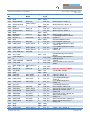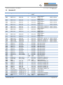
1
CM-i.MX6x Hardware User Manual Version 1.7 Contact Bluetechnix Waidhausenstraße 3/19 A-1140 Vienna AUSTRIA [email protected] http://www.bluetechnix.com Document No.: 100-1217-7 Date: 2014-09-04 © Bluetechnix 2014 Table of Contents 1 2 Introduction ...................................................................................................................................... 6 1.1 Overview ................................................................................................................................... 6 1.2 Key Features ............................................................................................................................. 7 1.3 Applications............................................................................................................................... 8 General Description .......................................................................................................................... 9 2.1 3 2.1.1 PMIC .................................................................................................................................. 9 2.1.2 Gigabit Ethernet ................................................................................................................. 9 2.1.3 DDR3 SDRAM .................................................................................................................. 10 2.1.4 eMMC Flash ..................................................................................................................... 10 2.1.5 MicroSD-Support ............................................................................................................. 10 2.1.6 SPI Flash .......................................................................................................................... 10 2.2 Boot Mode .............................................................................................................................. 10 2.3 Memory Map ........................................................................................................................... 11 Specifications ................................................................................................................................. 12 3.1 4 5 6 Functional Description .............................................................................................................. 9 Electrical Specifications .......................................................................................................... 12 3.1.1 Operating Conditions ....................................................................................................... 12 3.1.2 Maximum Ratings ............................................................................................................ 12 3.1.3 Power Outputs ................................................................................................................. 13 3.1.4 ESD Sensitivity ................................................................................................................. 13 3.1.5 Cooling ............................................................................................................................. 13 Connector Description ................................................................................................................... 15 4.1 Connector X1 .......................................................................................................................... 15 4.2 Connector X2 .......................................................................................................................... 17 4.3 Connector X3 .......................................................................................................................... 20 Application Information .................................................................................................................. 23 5.1 Supply Voltage Decoupling ..................................................................................................... 23 5.2 Power Outputs ........................................................................................................................ 23 5.3 Peripheral Supply .................................................................................................................... 23 5.4 Reset circuit ............................................................................................................................ 23 5.5 Differential pairs ...................................................................................................................... 23 5.6 Single-ended signals ............................................................................................................... 24 5.7 Application Example Schematics ........................................................................................... 24 Mechanical Outline ......................................................................................................................... 25 6.1 Top View ................................................................................................................................. 25 6.2 Bottom View ............................................................................................................................ 25 © Bluetechnix 2014 6.3 Side View................................................................................................................................. 26 6.4 Footprint .................................................................................................................................. 26 6.5 Connectors .............................................................................................................................. 27 7 Support ........................................................................................................................................... 28 7.1 General Support ...................................................................................................................... 28 7.2 Board Support Packages ........................................................................................................ 28 7.3 i.MX Software Support ............................................................................................................ 28 7.3.1 Linux................................................................................................................................. 28 7.3.2 Android............................................................................................................................. 28 7.3.3 Win CE ............................................................................................................................. 28 7.4 i.MX Design Services .............................................................................................................. 28 7.4.1 8 Upcoming Products and Software Releases .................................................................. 28 Ordering Information ...................................................................................................................... 29 8.1 9 Predefined mounting options for CM-i.MX6x ......................................................................... 29 Dependability ................................................................................................................................. 30 9.1 10 MTBF ....................................................................................................................................... 30 Product History ........................................................................................................................... 31 10.1 Version Information ............................................................................................................. 31 10.1.1 CM-i.MX6Q-C-C-Q24S2048F2N4096 (CM-i.MX6Q) ....................................................... 31 10.1.2 CM-i.MX6Q-C-I-Q24S2048F2N4096 (CM-i.MX6Q) ........................................................ 31 10.2 Anomalies ............................................................................................................................ 31 11 Document Revision History ........................................................................................................ 32 12 List of Abbreviations ................................................................................................................... 33 A List of Figures and Tables .............................................................................................................. 34 © Bluetechnix 2014 © Bluetechnix GmbH 2014 All Rights Reserved. The information herein is given to describe certain components and shall not be considered as a guarantee of characteristics. Terms of delivery and rights of technical change reserved. We hereby disclaim any warranties, including but not limited to warranties of non-infringement, regarding circuits, descriptions and charts stated herein. Bluetechnix makes and you receive no warranties or conditions, express, implied, statutory or in any communication with you. Bluetechnix specifically disclaims any implied warranty of merchantability or fitness for a particular purpose. Bluetechnix takes no liability for any damages and errors causing of the usage of this board. The user of this board is responsible by himself for the functionality of his application. He is allowed to use the board only if he has the qualification. More information is found in the General Terms and Conditions (AGB). Information For further information on technology, delivery terms and conditions and prices please contact Bluetechnix (http://www.bluetechnix.com). Warning Due to technical requirements components may contain dangerous substances. © Bluetechnix 2014 Hardware User Manual - CM-i.MX6x 1 Last change: 4 September 2014 Version 1.7 Introduction The SoM CM-i.MX6x is based on Freescale’s next generation, high-performance, power-efficient, consumer multimedia applications processor family i.MX6. The SoM is available for both, commercial and industrial temperature range. It addresses up to 2 GByte of DDR3-SDRAM, has an onboard SPI NOR-flash of 2MByte and an eMMC-Flash of 4GByte. The state of the art i.MX6 SoM in combination with the outstanding integration of several peripheral controllers, memory and voltage control, turn the CM-i.MX6x into a high-performance embedded platform for your future applications. 1.1 Overview Figure 1-1 shows the main components of the CM-i.MX6x. CAN1/2 I2C2/3 ECSPI2/3 Giga-ETH AUD4/6 2MB SPI-Flash GigaBitETH-Phy i.MX6 5V0 regulator Up to 2 GByte DDR3-SDRAM 4 GByte eMMC-Flash PMIC 100 Pin Expansion Connector HDMI PCIe 100 Pin Expansion Connector UART2/3/4/5 LVDS0/1 CM-i.MX6x PWM3/4 16-Bit CSI0 & MIPI 24-Bit DISP1 8-Bit USDHC3 8-Bit USDHC1 MIPI DSI JTAG SATA II CTRL CLK1/2 PWM1/2 LVDS0/1 USBH & USB-OTG S/PDIF GPIOs 100 Pin Expansion Connector Figure 1-1: Main Components of the CM-i.MX6x © Bluetechnix 2014 Page 6 | 34 Hardware User Manual - CM-i.MX6x 1.2 Key Features • • • Freescale Application Processor i.MX6 o Quad-Core – Industrial version MCIMX6Q6AVT10AC o Quad-Core – Commercial version MCIMX6Q5EYM10AC o Dual-Core – Industrial version MCIMX6D6AVT10AC o Dual-Core – Commercial version MCIMX6D5EYM10AC o Single-Core – Industrial version MCIMX6S6AVM08AB o Single-Core – Commercial version MCIMX6S8DVM10AB DDR3-SDRAM o Quad- and Dual-Core Industrial version MEM4G16D3EABG-125I DDR3-SDRAM Clock up to 533MHz 2GByte, 4x (32Mbit x16 x 8 banks, 4Gbit at 1.35V) o Quad- and Dual-Core Commercial version MEM4G16D3EABG-125 DDR3-SDRAM Clock up to 533MHz 2GByte, 4x (32Mbit x16 x 8 banks, 4Gbit at 1.35V) o Single-Core Industrial version 1GByte, MEM4G16D3EABG-125I DDR3-SDRAM Clock up to 533MHz 1GByte, 2x (32Mbit x16 x 8 banks, 4Gbit at 1.35V) o Single-Core Commercial version 1GByte, MEM4G16D3EABG-125 DDR3-SDRAM Clock up to 533MHz 1GByte, 2x (32Mbit x16 x 8 banks, 4Gbit at 1.35V) 4 GByte eMMC-Flash or MicroSD-card slot o Industrial version 4 GByte, KE4CN2H5C o • Last change: 4 September 2014 Version 1.7 Commercial version 4 GByte, H26M31002GPR 2 MByte SPI-Flash o 2MByte, M25PX16-VMN6TP © Bluetechnix 2014 Page 7 | 34 Hardware User Manual - CM-i.MX6x • PMIC o o o LTC3676EUJ#PBF Energy Management Power-up sequencer • Gigabit Ethernet PHY o KSZ9031RNXI • Interfaces o 4-5x UART o 2x SPI o 2x I2C o 2x CAN o 2x 8-Bit SDIO o 1x 24-Bit Parallel Display o 1x HDMI o 2x LVDS o 2x DSI-Lanes o 1x Gigabit Ethernet o 2x AUD o 1x S/PDIF o 1x 16-Bit CSI o 4x CSI-Lanes o 4x PWM o 2x CLK o 1x USBOTG o 1x USBH o 1x SATA II o 1x PCIe o GPIOs o CTRL o JTAG o Power Supply 1.3 Last change: 4 September 2014 Version 1.7 Applications • Tablets • Smart Mobile Devices • Human-Machine-Interface • 3D-Cameras • Medical Devices • Video Conference Systems • Imaging and Consumer Multimedia • Set Top Boxes • Video Conference Applications • Portable Media Players • Industrial Applications © Bluetechnix 2014 Page 8 | 34 Hardware User Manual - CM-i.MX6x General Description JTAG JTAG MIPI DSI MIPI DSI AUD4/6 AUD4/6 CLK1/2 SATA II SATA II PCIe PCIe I2C2/3 CLK1/2 I2C2/3 LVDS0/1 CAN1/2 LVDS0/1 CAN1/2 USB-OTG MIPI CSI USB-OTG MIPI CSI DRAM USBH 16-Bit CSI0 Micro-SD slot USBH 16-Bit CSI0 USDHC2 S/PDIF 24-Bit DISP1 4GByte eMMC-Flash S/PDIF 24-Bit DISP1 ECSPI1 + SS0 Freescale i.MX6 Processor GPIOs USDHC1/3 2MByte SPI-Flash Up to 2GByte DDR3-SDRAM ECSPI2/3 RGMII GPIOs USDHC1/3 Gbit ETH-PHY ECSPI2/3 I2C1 HDMI CTRL CM-i.MX6x PWM1/2/3/4 LTC3676 + 5V Buck/Boost CTRL PWM1/2/3/4 Giga-ETH Single Supply PWR HDMI Functional Description UART2/3/4/5 2.1 UART2/3/4/5 2 Last change: 4 September 2014 Version 1.7 Figure 2-1 Detailed block diagram of the CM-i.MX6x 2.1.1 PMIC The power supplies for the i.MX6 processor are generated with the PMIC LTC3676 from Linear Technology in conjunction with the 5V Buck-Boost-Converter. The PMIC can be configured through the I2C1 interface of the i.MX6. 2.1.2 Gigabit Ethernet The CM-i.MX6x has the Gigabit Ethernet PHY KSZ9031RNXI from Micrel onboard. The Gigabit Ethernet PHY is connected through RGMII with the i.MX6. © Bluetechnix 2014 Page 9 | 34 Hardware User Manual - CM-i.MX6x 2.1.3 Last change: 4 September 2014 Version 1.7 DDR3 SDRAM The CM-i.MX6x provides up to 2 GByte of DDR3 SDRAM onboard. 2.1.4 eMMC Flash The CM-i.MX6x provides 4 GByte of eMMC Flash onboard. The eMMC memory is connected through the USDHC2 interface with the i.MX6. 2.1.5 MicroSD-Support An optional MicroSD-slot can be mounted on the bottom side of the CM-i.MX6x. The MicroSD card shares the interface to the i.MX6 with the eMMC Flash (USDHC2). Both memories can be used simultaneously using the appropriate card identification mode (see Secure Digital Card Specification). 2.1.6 SPI Flash The CM-i.MX6x provides 2 MByte of SPI Flash connected to the ECSPI1 and SS0 as chip select signal. 2.2 Boot Mode The overall boot mode of the i.MX6 processor is determined by the BOOT_MODE[1:0] pins. For Internal Boot mode (BOOT_MODE[1:0] = 10), boot media is selected either by internal fuses, or by GPIOs which are sampled at power-up. For burning boot fuses, please consult the i.MX6 Reference Manual and the Software User Manual for the CM-i.MX6x. If boot media selection by GPIO sampling is desired, pull-down or pull-up resistors must be added to the specified pins. See chapter 0 for the voltage level of these pins. Consult the Hardware Development Guide for i.MX 6Quad, 6Dual, 6DualLite, 6Solo Families of Applications Processors (Freescale Document ID IMX6DQ6SDLHDG) for pull-down/-up recommendations. Table 2-1 contains permitted configuration options of BOOT_MODE pins, where 0 means logic low and 1 means logic high. Consult aforementioned Hardware Development Guide for how to achieve these logic levels. CM-i.MX6x Pin Internal Boot (see below) 0 1 BOOT_MODE0 BOOT_MODE1 Serial Downloader (USB) 1 0 Boot From Fuses 0 0 Table 2-1: Boot mode pins Table 2-2 contains the fuse/GPIO settings for the Internal Boot mode. An empty cell means that this pin’s value is not considered for a specific boot setting. A cell marked with X means that the setting depends on your base board/custom boot flash. Please consult the i.MX 6Dual/6Quad Applications Processor Reference Manual (Freescale Doc. ID IMX6DQRM) to get more information. CM-i.MX6x Pin eFuse Name DISP1.DAT9 DISP1.DAT8 BOOT_CFG10 BOOT_CFG11 © Bluetechnix 2014 SPI flash on SoM (ECSPI1) External SPI flash (ECSPI3) External SD/MMC (USDHC1) X 0 eMMC on SoM (USDHC2) 0 External SD/MMC (USDHC3) X X External SATA disk Page 10 | 34 Hardware User Manual - CM-i.MX6x CM-i.MX6x Pin eFuse Name DISP1.DAT7 DISP1.DAT6 DISP1.DAT5 DISP1.DAT4 DISP1.DAT3 DISP1.DAT2 DISP1.DAT1 DISP1.DAT0 DISP1.PIN15 DISP1.PIN2 DISP1.PIN3 GPIO.3_13 GPIO.3_14 DISP1.PIN1 DISP1.CLK DISP1.DAT12 DISP1.DAT13 DISP1.DAT14 DISP1.DAT15 DISP1.DAT16 DISP1.DAT17 DISP1.DAT18 DISP1.DAT19 GPIO.5_0 ECSPI2.SS1 DISP1.DAT11 DISP1.DAT10 ECSPI2.SS0 ECSPI1.SS0 UART3.RTS BOOT_CFG12 BOOT_CFG13 BOOT_CFG14 BOOT_CFG15 BOOT_CFG16 BOOT_CFG17 BOOT_CFG20 BOOT_CFG21 BOOT_CFG22 BOOT_CFG23 BOOT_CFG24 BOOT_CFG25 BOOT_CFG26 BOOT_CFG27 BOOT_CFG30 BOOT_CFG31 BOOT_CFG32 BOOT_CFG33 BOOT_CFG34 BOOT_CFG35 BOOT_CFG36 BOOT_CFG37 BOOT_CFG40 BOOT_CFG41 BOOT_CFG42 BOOT_CFG43 BOOT_CFG44 BOOT_CFG45 BOOT_CFG46 BOOT_CFG47 Last change: 4 September 2014 Version 1.7 SPI flash on SoM (ECSPI1) External SPI flash (ECSPI3) 1 1 0 0 1 1 0 0 External SD/MMC (USDHC1) X X X X 1 0 0 0 X 0 0 X X X eMMC on SoM (USDHC2) 0 0 1 1 0 0 0 0 1 0 0 1 0 External SD/MMC (USDHC3) X X X X 1 0 0 X X 0 1 X X X External SATA disk 0 1 0 0 X X X X X Default 0 (792MHz ARM clock) 0 0 0 1 0 0 Default 0 (ROM code enables MMU and L1 D-cache) Default 0 (ROM code enables L1 I-cache) 0 1 0 X X X Default 0 Table 2-2: Boot configuration pins 2.3 Memory Map Component 2 GiB DDR3-SDRAM Memory area 0x1000_0000 - 0x8FFF_FFFF Chip select DRAM_CS0 Please consult the i.MX6 Reference Manual for the complete memory maps. © Bluetechnix 2014 Page 11 | 34 Hardware User Manual - CM-i.MX6x 3 Last change: 4 September 2014 Version 1.7 Specifications 3.1 Electrical Specifications 3.1.1 Operating Conditions Symbol VIN I3V3 VP_3V0_STBY IP_3V0_STBY VOH VOL VIH VIL ISIO IIN Parameter Input supply voltage Input supply current @ VIN=3.3V Input current (no pull-up/down) Input current (47 kΩ pull-up) Input current (100 kΩ pull-up) Input current (100 kΩ pull-down) ISLEEP IIDLE ITYP IHIBERNATE fCCLKC fCCLKQI Min 2.7 150 2.8 @ VP_3V0_STBY=3.0V High level output voltage Low level output voltage High level DC input voltage Low level DC input voltage IO sink current Input current (22 kΩ pull-up) IDEEPSLEEP Test Vin=0V Vin=OVDD Vin=0V Vin=OVDD Vin=0V Vin=OVDD Vin=0V Vin=OVDD Vin=0V Vin=OVDD 3.15 2.3 0 -1 Typ 3.0 0.6 - - - - - - - 5.5 2040 3.3 3.45 0.15 3.3 1 7 1 Unit V mA V mA V V V V mA µA - 150 212 1 100 1 48 1 1 48 - - 190 600 570 - mA mA mA - 3.6 - mA - - 1000 MHz - - 1000 MHz - VIN current in deep sleep mode @ VIN=3.3V VIN current in sleep mode @ VIN=3.3V VIN current in idle mode @ VIN=3.3V VIN current in idle mode with cores running at 400 MHz @ VIN=3.3V VIN current in hibernate state @ VIN=3.3V Core clock frequency for commercial grade modules Core clock frequency for industrial grade modules Max µA µA µA µA mA Table 3-1: Electrical characteristics 3.1.2 Maximum Ratings Stressing the device above the rating listed in the absolute maximum ratings table may cause permanent damage to the device. These are stress ratings only. Operation of the device at these or any other conditions greater than those indicated in the operating sections of this specification is not implied. Exposure to absolute maximum rating conditions for extended periods may affect device reliability. Symbol VIO VIN IOH /IOL TAMBC TAMBI © Bluetechnix 2014 Parameter Input or output voltage Input supply voltage Current per pin Ambient temperature for consumer grade Ambient temperature for industrial grade Min -0.5 -0.3 0 0 -40 Max 3.6 6 7 70* 105* Unit V V mA °C °C Page 12 | 34 Hardware User Manual - CM-i.MX6x Symbol TSTO TSLD φAMB Last change: 4 September 2014 Version 1.7 Parameter Storage temperature Solder temperature for 10 seconds Relative ambient humidity Min -40 Max 150 260 90 Unit °C °C % Table 3-2: Absolute maximum ratings If extreme high ambient temperatures are expected (75°C in industrial environments or 60°C for commercial products), the user has to apply a heat dissipator on CPU and DDR-RAM (avoid heat accumulation!). In addition the die temperature should be monitored regularly, so that the CPU and RAM clock can be throttled if necessary. * 3.1.3 Power Outputs The CM-i.MX6x provides voltage references for the power domains used by the i.MX6. This power outputs are intended as voltage references. Symbol Vref_diff Vref_3V3 Vref_5V0 Vref_2V5 Vref_CTRL Description Reference voltage for differential signals and others Reference voltage for 3V3 Reference voltage for 5V0 Reference voltage for 2V5 Reference voltage for control signals U [V] 2.5 Imax [mA] 10 3.3 5.0 2.5 3.0 200 250 120 10 Table 3-3: Power Outputs 3.1.4 ESD Sensitivity ESD (electrostatic discharge) sensitive device. Charged devices and circuit boards can discharge without detection. Although this product features patented or proprietary protection circuitry, damage may occur on devices subjected to high energy ESD. Therefore, proper ESD precautions should be taken to avoid performance degradation or loss of functionality. 3.1.5 Cooling If the SoM is subject to high performance applications a cooling system should be planned to prevent damage to and guarantee the full functionality of the SoM. The requirement of a cooling system depends also from the ambient temperature. The following test was performed in a conditioning cabinet: Firmware A test image based on the Linux board support package, which tests periodically/enables • • • • eMMC non-volatile storage SPI boot flash HDMI output GPU Results (without any cooling measures) © Bluetechnix 2014 Page 13 | 34 Hardware User Manual - CM-i.MX6x Last change: 4 September 2014 Version 1.7 The die temperature was measured to be 23 to 26°C higher than the ambient temperature. See Table 3-4 for details. Ambient temperature -20°C -10°C 0°C 10°C 20°C 30°C 40°C 50°C 60°C 70°C 80°C 85°C ARM cores frequency 996 MHz 996 MHz 996 MHz 996 MHz 996 MHz 996 MHz 996 MHz 996 MHz 996 MHz 396 MHz1) 396 MHz1) Processor shut-down at 100°C die temperature1) i.MX6Q die temperature 3°C 14°C 24°C 33°C 45°C 55°C 66°C 75°C 86°C 86°C 96°C Table 3-4: Ambient vs. die temperatures, no heat sink Note 1): These cooling measures are implemented in the default Linux BSP. Results (with heat sink) Heat sink type: MBH29002-33P/2.6 (29mm x 29mm x 33mm) See Table 3-5 for details. Ambient temperature 30°C 50°C ARM cores frequency 996 MHz 996 MHz i.MX6Q die temperature 34°C 54°C Table 3-5: Ambient vs. die temperatures, with heat sink © Bluetechnix 2014 Page 14 | 34 Hardware User Manual - CM-i.MX6x 4 Last change: 4 September 2014 Version 1.7 Connector Description For a detail signal description please consult the i.MX6 reference manual, available on the Freescale web site. 4.1 Connector X1 Pin No. 1 Signal Name ECSPI2.MISO i.MX6 Ball Name EIM_OE 2 ECSPI2.MOSI EIM_CS1 3 ECSPI2.SCLK EIM_CS0 4 ECSPI2.SS0 EIM_RW 5 ECSPI2.SS1 EIM_LBA 6 Vref_3V3 Type Voltage Level Vref_3V3 Function O Vref_3V3 SPI MOSI / GPIO2_24 O Vref_3V3 SPI Clock / GPIO2_23 O Vref_3V3 SPI Select0 / GPIO2_26 O Vref_3V3 SPI Select1 / GPIO2_27 PWR 3V3 3.3V Voltage Reference I Boot SPI MISO / GPIO2_25 7 ECSPI3.MISO DISP0_DAT2 I Vref_3V3 SPI MISO / GPIO4_23 8 ECSPI3.MOSI DISP0_DAT1 O Vref_3V3 SPI MOSI / GPIO4_22 9 ECSPI3.SCLK DISP0_DAT0 O Vref_3V3 SPI CLK / GPIO4_21 10 ECSPI3.SS0 DISP0_DAT3 O Vref_3V3 SPI Select0 / GPIO4_24 11 ECSPI3.SS1 DISP0_DAT4 O Vref_3V3 SPI Select1 / GPIO4_25 12 Vref_3V3 PWR 3V3 3.3V Voltage Reference 13 SD1.CMD SD1_CMD O Vref_3V3 SD Command / GPIO1_18 14 SD1.CLK SD1_CLK O Vref_3V3 SD Clock / GPIO1_20 BOOT_ CFG45 BOOT_ CFG42 15 SD1.DAT0 SD1_DAT0 I/O Vref_3V3 SD Data0 / GPIO1_16 16 SD1.DAT1 SD1_DAT1 I/O Vref_3V3 SD Data1 / GPIO1_17 17 SD1.DAT2 SD1_DAT2 I/O Vref_3V3 SD Data2 / GPIO1_19 18 SD1.DAT3 SD1_DAT3 I/O Vref_3V3 SD Data3 / GPIO1_21 19 SD1.CD gpio1_1 I Vref_3V3 SD Card Detect / GPIO1_24 20 GPIO3_14 EIM_DA14 I/O Vref_3V3 GPIO3_14 21 GND PWR GND 22 UART3.RTS EIM_EB3 O Vref_3V3 UART Request To Send / GPIO2_31 23 UART3.CTS EIM_D23 I Vref_3V3 UART Clear To Send / GPIO3_23 24 UART3.TX EIM_D24 O Vref_3V3 UART Transmit Data / GPIO3_24 25 UART3.RX EIM_D25 I Vref_3V3 UART Receive Data / GPIO3_25 26 Vref_3V3 PWR 3V3 3.3V Voltage Reference BOOT_ CFG26 BOOT_ CFG47 27 UART2.CTS SD4_DAT6 I Vref_3V3 UART Clear To Send / GPIO2_14 28 UART2.RTS SD4_DAT5 O Vref_3V3 UART Request To Send / GPIO2_13 29 UART2.TX SD4_DAT7 O Vref_3V3 UART Transmit Data / GPIO2_15 30 UART2.RX SD4_DAT4 I Vref_3V3 UART Receive Data / GPIO2_12 31 GND PWR GND 32 DISP1.PIN1 O Vref_3V3 DISP1 Pin15 / GPIO3_15 33 Vref_3V3 PWR 3V3 3.3V Voltage Reference © Bluetechnix 2014 EIM_DA15 BOOT_ CFG27 Page 15 | 34 Hardware User Manual - CM-i.MX6x Pin No. 34 Signal Name Last change: 4 September 2014 Version 1.7 AUD4.RXC i.MX6 Ball Name DISP0_DAT19 Type I Voltage Level Vref_3V3 35 AUD4.RXFS DISP0_DAT18 I Vref_3V3 36 AUD4.RXD DISP0_DAT23 I Vref_3V3 Function AUD Receive Clock / GPIO5_13 AUD Receive Frame Sync / GPIO5_12 AUD Receive Data / GPIO5_17 37 AUD4.TXC DISP0_DAT20 O Vref_3V3 AUD Transmit Clock / GPIO5_14 38 AUD4.TXD DISP0_DAT21 O Vref_3V3 39 AUD4.TXFS DISP0_DAT22 O Vref_3V3 40 Vref_3V3 PWR 3V3 AUD Transmit Data / GPIO5_15 AUD Transmit Frame Sync / GPIO5_16 3.3V Voltage Reference 41 I2C2.SCL KEY_COL3 O Vref_3V3 I2C Clock / GPIO4_12 42 I2C2.SDA KEY_ROW3 I/O Vref_3V3 I2C Data / GPIO4_13 43 I2C3.SCL gpio1_5 O Vref_3V3 I2C Clock / GPIO1_5 44 I2C3.SDA gpio1_6 I/O Vref_3V3 I2C Data / GPIO1_6 45 Vref_3V3 PWR 3V3 3.3V Voltage Reference 46 JTAG.TCK JTAG_TCK I Vref_3V3 JTAG Test Clock 47 JTAG.TMS JTAG_TMS I Vref_3V3 JTAG Test Mode Select 48 JTAG.TDI JTAG_TDI I Vref_3V3 JTAG Test Data Input 49 JTAG.TDO JTAG_TDO O Vref_3V3 JTAG Test Data Output 50 JTAG.TRSTB JTAG_TRSTB I Vref_3V3 JTAG Test Reset 51 NC 52 JTAG.MOD JTAG_MOD I Vref_3V3 JTAG Mode Selection 53 ETH.LED_ACT O Vref_2V5 ETH Activity LED Driver 54 ETH.LED_SPD O Vref_2V5 ETH Speed LED Driver 55 GPIO.1_29 I/O Vref_2V5 ENET TXD1 / GPIO1_29 56 ETH.TXRX_A_N I/O 3V3 ETH Data A- 57 ETH.TXRX_A_P I/O 3V3 ETH Data A+ 58 GND PWR GND 59 ETH.TXRX_B_N I/O 3V3 ETH Data B- 60 ETH.TXRX_B_P I/O 3V3 ETH Data B+ ENET_TXD1 61 GND PWR GND 62 CAN1.TX KEY_COL2 O Vref_3V3 CAN Transmit Data / GPIO4_10 63 CAN1.RX KEY_ROW2 I Vref_3V3 CAN Receive Data / GPIO4_11 64 Vref_3V3 PWR 3V3 3.3V Voltage Reference 65 UART4.RX KEY_ROW0 I Vref_3V3 UART Receive Data / GPIO4_7 66 UART4.TX KEY_COL0 O Vref_3V3 UART Transmit Data / GPIO4_6 67 GND PWR GND Power Ground 68 VIN PWR VIN Power Supply 69 VIN PWR VIN Power Supply 70 VIN PWR VIN Power Supply 71 VIN PWR VIN Power Supply 72 VIN PWR VIN Power Supply 73 GND PWR GND Power Ground 74 ETH.TXRX_C_N I/O © Bluetechnix 2014 Boot ETH Data CPage 16 | 34 Hardware User Manual - CM-i.MX6x Last change: 4 September 2014 Version 1.7 Pin No. 75 Signal Name i.MX6 Ball Name Type Voltage Level Function ETH.TXRX_C_P I/O 76 GND PWR GND 77 ETH.TXRX_D_N I/O 3V3 ETH Data D- 78 ETH.TXRX_D_P I/O 3V3 ETH Data D+ 79 Vref_diff PWR 2V5 2.5V Voltage Reference 80 HDMI.CLK_N HDMI_CLKM O Vref_diff HDMI Clock- 81 HDMI.CLK_P HDMI_CLKP O Vref_diff HDMI Clock+ 82 HDMI.D0_N HDMI_D0M O Vref_diff HDMI Data0- 83 HDMI.D0_P HDMI_D0P O Vref_diff HDMI Data0+ 84 HDMI.D1_N HDMI_D1M O Vref_diff HDMI Data1- 85 HDMI.D1_P HDMI_D1P O Vref_diff HDMI Data1+ 86 HDMI.D2_N HDMI_D2M O Vref_diff HDMI Data2- 87 HDMI.D2_P HDMI_D2P O Vref_diff HDMI Data2+ 88 SD1.DAT4 NANDF_D0 I/O Vref_3V3 SD Data3 / GPIO2_0 89 SD1.DAT5 NANDF_D1 I/O Vref_3V3 SD Data3 / GPIO2_1 90 SD1.DAT6 NANDF_D2 I/O Vref_3V3 SD Data3 / GPIO2_2 91 SD1.DAT7 NANDF_D3 I/O Vref_3V3 SD Data3 / GPIO2_3 92 GND PWR GND 93 GPIO.4_5 GPIO_19 I/O Vref_3V3 94 DSI.CLK_N DSI_CLK0M O Vref_diff DSI Clock- 95 DSI.CLK_P DSI_CLK0P O Vref_diff DSI Clock+ 96 DSI.D0_N DSI_D0M O Vref_diff DSI Data0- 97 DSI.D0_P DSI_D0P O Vref_diff DSI Data0+ 98 DSI.D1_N DSI_D1M O Vref_diff DSI Data1- 99 DSI.D1_P DSI_D1P O Vref_diff DSI Data1+ 100 Vref_diff PWR 2V5 2.5V Voltage Reference Boot ETH Data C+ GPIO_19 / GPIO4_5 Table 4-1: Connector description X1 4.2 Connector X2 Pin No. 101 102 103 104 105 106 107 108 109 110 Signal Name 111 112 GPIO1_3 GPIO1_0 O O I/O I/O I/O I/O PWR PWR I O Voltage Level Vref_diff Vref_diff Vref_3V3 Vref_3V3 Vref_3V3 Vref_3V3 2V5 Vref_5V0 Vref_3V3 Vref_3V3 SATA Transmit DataSATA Transmit Data+ GPIO5_6 GPIO5_7 Clock 2 output Clock 2 output + 2.5V Voltage Reference USB VBUS USB Over Current / GPIO1_3 USB Power Enable / GPIO1_0 GPIO.5_0 EIM_WAIT I/O Vref_3V3 GPIO5_0 USB_OTG.PWR EIM_D22 O Vref_3V3 USB Power Enable / GPIO3_22 SATA.TX_N SATA.TX_P GPIO.5_6 GPIO.5_7 GPIO.6_7 GPIO.6_8 Vref_diff USB_H.VBUS USB_H.OC USB_H.PWR © Bluetechnix 2014 i.MX Ball Name SATA_TXM SATA_TXP DISP0_DAT12 DISP0_DAT13 NANDF_CLE NANDF_ALE Type Function Boot BOOT_ CFG41 Page 17 | 34 Hardware User Manual - CM-i.MX6x Pin No. 113 114 115 Signal Name Function I PWR I Voltage Level Vref_3V3 GND Vref_3V3 116 SPDIF.EXTCLK I Vref_diff SPDIF EXTCLK / GPIO1_25 117 118 119 120 121 122 123 124 125 GND SPDIF.IN SPDIF.PLOCK GND SPDIF.OUT Vref_2V5 GPIO.6_31 GND EPIT_OUT2 EIM_D20 PWR I O PWR O PWR I/O PWR O GND Vref_3V3 Vref_3V3 GND Vref_3V3 2V5 Vref_3V3 GND Vref_3V3 126 PWM_OUT1 DISP0_DAT8 O Vref_3V3 127 PWM_OUT2 DISP0_DAT9 O Vref_3V3 128 129 GPIO.5_10 CTRL.PWR_ON DISP0_DAT16 EIM_D29 I/O I Vref_3V3 130 Vref_CTRL PWR 3V0 I Vref_CTRL I Vref_CTRL O Vref_CTRL O Vref_CTRL Vref_3V3 3V0 GND Vref_3V3 Vref_3V3 USB_OTG.ID GND SPDIF.SRCLK 132 CTRL.nRESET_I N CTRL.TAMPER 133 CTRL.nON 131 i.MX Ball Name ENET_RX_ER Last change: 4 September 2014 Version 1.7 GPIO1_8 ENET_CRS_D V GPIO_16 GPIO1_7 GPIO_17 EIM_BCLK TAMPER Type 135 136 137 138 139 PMIC_STBY_RE Q WDOG1_B 3V0_STBY GND CAN2.RX CAN2.TX PMIC_STBY_R EQ GPIO1_9 KEY_ROW4 KEY_COL4 O PWR PWR I O 140 PWM_OUT3 SD4_DAT1 O Vref_3V3 141 PWM_OUT4 SD4_DAT2 O Vref_3V3 142 143 144 Vref_3V3 EPIT_OUT1 AUD6.RXC EIM_D19 DISP0_DAT6 PWR O I 3V3 Vref_3V3 Vref_3V3 145 AUD6.RXFS DISP0_DAT5 I Vref_3V3 146 AUD6.RXD DI0_PIN4 I Vref_3V3 147 AUD6.TXC DI0_PIN15 O Vref_3V3 148 AUD6.TXD DI0_PIN2 O Vref_3V3 149 AUD6.TXFS DI0_PIN3 O Vref_3V3 150 151 152 GND GND ECSPI1.SS1 DISP0_DAT15 PWR PWR I/O GND GND Vref_3V3 134 © Bluetechnix 2014 Boot USB ID / GPIO1_1 SPDIF SRCLK / GPIO1_8 SPDIF Input / GPIO7_11 SPDIF PLOCK / GPIO1_7 SPDIF Output / GPIO7_12 2.5V Voltage Reference (LDO) GPIO6_31 AUDIO Headphone GND EPIT2 Output / GPIO3_20 Pulse Width Modulation Output / GPIO4_29 Pulse Width Modulation Output / GPIO4_30 GPIO5_10 Voltage Reference for Control Signals External Reset Input (Short to GND for Reset) Tamper Start-Up PMIC if PIN is low for 400ms Don’t use this Pin as GPIO! 3V0 Standby Voltage CAN RX / GPIO4_15 CAN TX / GPIO4_14 Pulse Width Modulation / GPIO2_9 Pulse Width Modulation / GPIO2_10 3.3V Voltage Reference EPIT1 Output / GPIO3_19 AUD Receive Clock / GPIO4_27 AUD Receive Frame Sync / GPIO4_26 AUD Receive Data / GPIO4_20 AUD Transmit Clock / GPIO4_17 AUD Transmit Data / GPIO4_18 AUD Transmit Frame Sync / GPIO4_19 ECSPI1_SS1 / GPIO5_9 Page 18 | 34 Hardware User Manual - CM-i.MX6x Pin No. 153 154 155 Signal Name Last change: 4 September 2014 Version 1.7 Type GPIO.2_8 GPIO.7_10 GPIO.5_11 i.MX Ball Name SD4_DAT0 SD4_CLK DISP0_DAT17 156 GPIO.3_13 EIM_DA13 157 158 159 160 161 162 163 164 165 166 167 168 169 170 171 172 173 174 175 176 177 178 179 180 181 182 183 184 185 186 187 188 189 190 191 192 193 194 195 196 197 198 199 200 Vref_3V3 GND GPIO.5_5 GPIO.4_31 GPIO.4_28 GPIO.4_16 Vref_diff CTRL.BM1 CTRL.BM0 VIN VIN VIN VIN GND GND GND GND SD3.VSELECT SD3.RST SD3.DAT7 SD3.DAT6 SD3.DAT5 SD3.DAT4 Vref_3V3 SD3.DAT3 SD3.DAT2 SD3.DAT1 SD3.DAT0 SD3.CLK SD3.CMD GND USB_OTG.VBUS USB_OTG.D_P USB_OTG.D_N GND USB_H.D_P USB_H.D_N Vref_5V0 GPIO.6_9 CLK2.CLK_P CLK2.CLK_N GND SATA.RX_P SATA.RX_N DISP0_DAT11 DISP0_DAT10 DISP0_DAT7 DI0_DISP_CLK BOOTMODE1 BOOTMODE0 GPIO_18 SD3_RST SD3_DAT7 SD3_DAT6 SD3_DAT5 SD3_DAT4 SD3_DAT3 SD3_DAT2 SD3_DAT1 SD3_DAT0 SD3_CLK SD3_CMD USB_OTG_DP USB_OTG_DN USB_H1_DP USB_H1_DN NANDF_WP_B CLK2_P CLK2_N SATA_RXP SATA_RXM I/O I/O I/O Voltage Level Vref_3V3 Vref_3V3 Vref_3V3 Function GPIO2_8 GPIO7_10 GPIO5_11 I/O Vref_3V3 GPIO3_13 PWR PWR I/O I/O I/O I/O PWR I I PWR PWR PWR PWR PWR PWR PWR PWR O O I/O I/O I/O I/O PWR I/O I/O I/O I/O O O PWR PWR I/O I/O PWR I/O I/O PWR I/O I/O I/O PWR I I 3V3 GND Vref_3V3 Vref_3V3 Vref_3V3 Vref_3V3 2V5 Vref_CTRL Vref_CTRL VIN VIN VIN VIN GND GND GND GND Vref_3V3 Vref_3V3 Vref_3V3 Vref_3V3 Vref_3V3 Vref_3V3 3V3 Vref_3V3 Vref_3V3 Vref_3V3 Vref_3V3 Vref_3V3 Vref_3V3 GND Vref_5V0 3V0 3V0 GND 3V0 3V0 5V0 Vref_3V3 Vref_diff Vref_diff GND Vref_diff Vref_diff 3.3V Voltage Reference Boot BOOT_ CFG25 GPIO5_5 GPIO4_31 GPIO4_28 GPIO4_16 2.5V Voltage Reference Boot Mode1 Boot Mode0 Power Supply Power Supply Power Supply Power Supply Power Ground Power Ground Power Ground Power Ground SDIO VSELECT / GPIO7_13 SDIO Reset / GPIO7_8 SDIO Data7 / GPIO6_17 SDIO Data6 / GPIO6_18 SDIO Data5 / GPIO7_0 SDIO Data4 / GPIO7_1 3.3V Voltage Reference SDIO Data3 / GPIO7_7 SDIO Data2 / GPIO7_6 SDIO Data1 / GPIO7_5 SDIO Data0 / GPIO7_4 SDIO CLK / GPIO7_3 SDIO Command / GPIO7_2 USB VBUS USB OTP Data+ USB OTP DataUSB Data+ USB DataUSB Voltage Reference GPIO6_9 GPIO6_8 GPIO6_7 SATA Receive Data+ SATA Receive Data- Table 4-2: Connector description X2 © Bluetechnix 2014 Page 19 | 34 Hardware User Manual - CM-i.MX6x 4.3 Last change: 4 September 2014 Version 1.7 Connector X3 Pin No. Signal Name 201 Vref_diff 202 DISP1.D14 203 PWR Voltage Level 2V5 EIM_A19 O Vref_3V3 DISP1.D15 EIM_A20 O Vref_3V3 204 DISP1.D16 EIM_A21 O Vref_3V3 205 DISP1.D17 EIM_A22 O Vref_3V3 206 207 DISP1.D18 DISP1.D19 EIM_A23 EIM_A24 O O Vref_3V3 Vref_3V3 208 DISP1.D20 EIM_D31 O Vref_3V3 209 DISP1.D21 EIM_D30 O Vref_3V3 210 DISP1.D22 EIM_D26 O Vref_3V3 211 DISP1.D23 EIM_D27 O Vref_3V3 212 213 214 215 216 217 218 219 220 221 222 223 224 225 226 227 228 229 230 231 232 233 234 235 236 237 238 239 240 241 DISP1.CLK DISP1.PIN2 DISP1.PIN3 DISP1.PIN15 CSI.D0_P CSI.D0_N CSI.D1_P CSI.D1_N CSI.D2_P CSI.D2_N CSI.D3_P CSI.D3_N CSI.CLK_P CSI.CLK_N GND UART5.TX UART5.RX GND CSI0.D9 CSI0.D8 CSI0.D7 CSI0.D6 CSI0.D5 CSI0.D4 32K_OUT LVDS0.CLK_P LVDS0.CLK_N LVDS0.TX0_P LVDS0.TX0_N GND EIM_A16 EIM_DA11 EIM_DA12 EIM_DA10 CSI_D0P CSI_D0M CSI_D1P CSI_D1M CSI_D2P CSI_D2M CSI_D3P CSI_D3M CSI_CLK0P CSI_CLK0M O O O O I I I I I I I I O O PWR O I PWR I I I I I I O O O O O PWR Vref_3V3 Vref_3V3 Vref_3V3 Vref_3V3 Vref_diff Vref_diff Vref_diff Vref_diff Vref_diff Vref_diff Vref_diff Vref_diff Vref_diff Vref_diff GND Vref_3V3 Vref_3V3 GND Vref_3V3 Vref_3V3 Vref_3V3 Vref_3V3 Vref_3V3 Vref_3V3 Vref_diff Vref_diff Vref_diff Vref_diff Vref_diff GND © Bluetechnix 2014 i.MX Ball Name KEY_COL1 KEY_ROW1 CSI0_D9 CSI0_D8 CSI0_D7 CSI0_D6 CSI0_D5 CSI0_D4 ENET_RXD0 LVDS0_CLK_P LVDS0_CLK_N LVDS0_TX0_P LVDS0_TX0_N Type Function 2.5V Voltage Reference DISP Data14 / GPIO2_19 DISP Data15 / GPIO2_18 DISP Data16 / GPIO2_17 DISP Data17 / GPIO2_16 DISP Data18 / GPIO6_6 DISP Data19 / GPIO5_4 DISP Data20 / GPIO3_31 DISP Data21 / GPIO3_30 DISP Data22 / GPIO3_26 DISP Data23 / GPIO3_27 DISP Clock / GPIO2_22 DISP Pin1 / GPIO3_11 DISP Pin2/ GPIO3_12 DISP Pin3/ GPIO3_10 MIPI CSI Lane0+ MIPI CSI Lane0MIPI CSI Lane1+ MIPI CSI Lane1MIPI CSI Lane2+ MIPI CSI Lane2MIPI CSI Lane3+ MIPI CSI Lane3MIPI CSI Clock+ MIPI CSI ClockSignal Ground UART5 RX / GPIO4_9 UART5 TX / GPIO4_8 Signal Ground CSI Data9 / GPIO5_27 CSI Data8 / GPIO5_26 CSI Data7 / GPIO5_25 CSI Data6 / GPIO5_24 CSI Data5 / GPIO5_23 CSI Data4 / GPIO5_22 32K Output / GPIO1_27 LVDS Clock+ LVDS ClockLVDS Transmit Data0+ LVDS Transmit Data0Signal Ground Boot BOOT_CFG33 BOOT_CFG34 BOOT_CFG35 BOOT_CFG36 BOOT_CFG37 BOOT_CFG40 BOOT_CFG30 BOOT_CFG23 BOOT_CFG24 BOOT_CFG22 Page 20 | 34 Hardware User Manual - CM-i.MX6x Last change: 4 September 2014 Version 1.7 Pin No. Signal Name i.MX Ball Name Type 242 243 244 245 246 247 248 249 250 251 252 253 254 LVDS0.TX1_P LVDS0.TX1_N LVDS0.TX2_P LVDS0.TX2_N LVDS0.TX3_P LVDS0.TX3_N Vref_diff CLK1.CLK_N CLK1.CLK_P PCIE.RX_N PCIE.RX_P PCIE.TX_N PCIE.TX_P LVDS0_TX1_P LVDS0_TX1_N LVDS0_TX2_P LVDS0_TX2_N LVDS0_TX3_P LVDS0_TX3_N CLK1_N CLK1_P PCIE_RXM PCIE_RXP PCIE_TXM PCIE_TXP O O O O O O PWR O O I I O O Voltage Level Vref_diff Vref_diff Vref_diff Vref_diff Vref_diff Vref_diff 2V5 Vref_diff Vref_diff Vref_diff Vref_diff Vref_diff Vref_diff 255 EN_PERI EIM_A25 O Vref_3V3 256 257 258 HDMI.HPD HDMI.DDCCEC Vref_3V3 HDMI_HPD HDMI_DDCCEC I I/O PWR Vref_diff Vref_3V3 3V3 259 CSI0.DATA_EN CSI0_DATA_EN I Vref_3V3 260 CSI0.PIXCLK CSI0_PIXCLK I Vref_3V3 261 CSI0.HSYNC CSI0_HSYNC I Vref_3V3 262 CSI0.VSYNC CSI0_VSYNC I Vref_3V3 263 264 265 266 267 268 269 270 271 272 273 274 275 276 277 278 279 280 281 282 283 284 285 GND CSI0.D19 CSI0.D18 CSI0.D17 CSI0.D16 CSI0.D15 Vref_3V3 CSI0.D14 CSI0.D13 CSI0.D12 CSI0.D11 CSI0.D10 Vref_diff LVDS1.CLK_N LVDS1.CLK_P LVDS1.TX0_N LVDS1.TX0_P LVDS1.TX1_N LVDS1.TX1_P LVDS1.TX2_N LVDS1.TX2_P LVDS1.TX3_N LVDS1.TX3_P LVDS1_CLK_N LVDS1_CLK_P LVDS1_TX0_N LVDS1_TX0_P LVDS1_TX1_N LVDS1_TX1_P LVDS1_TX2_N LVDS1_TX2_P LVDS1_TX3_N LVDS1_TX3_P PWR I I I I I PWR I I I I I PWR O O O O O O O O O O GND Vref_3V3 Vref_3V3 Vref_3V3 Vref_3V3 Vref_3V3 3V3 Vref_3V3 Vref_3V3 Vref_3V3 Vref_3V3 Vref_3V3 2V5 Vref_diff Vref_diff Vref_diff Vref_diff Vref_diff Vref_diff Vref_diff Vref_diff Vref_diff Vref_diff 286 DISP1.D13 EIM_A18 O Vref_3V3 © Bluetechnix 2014 CSI0_D19 CSI0_D18 CSI0_D17 CSI0_D16 CSI0_D15 CSI0_D14 CSI0_D13 CSI0_D12 CSI0_D11 CSI0_D10 Function Boot LVDS Transmit Data1+ LVDS Transmit Data1LVDS Transmit Data2+ LVDS Transmit Data2LVDS Transmit Data3+ LVDS Transmit Data32.5V Voltage Reference Clock1Clock1+ PCIe ReceivePCIe Receive+ PCIe TransmitPCIe Transmit+ Enable Signal for Peripheral Supply HDMI Hot Plug Detect HDMI DDC/CEC CSI Data Enable / GPIO5_20 CSI Pixel Clock / GPIO5_18 CSI Data Enable / GPIO5_19 CSI Vertical Sync / GPIO5_21 Signal Ground CSI Data19 / GPIO6_5 CSI Data18 / GPIO6_4 CSI Data17 / GPIO6_3 CSI Data16 / GPIO6_2 CSI Data15 / GPIO6_1 3.3V Voltage Reference CSI Data14 / GPIO6_0 CSI Data13 / GPIO5_31 CSI Data12 / GPIO5_30 CSI Data11 / GPIO5_29 CSI Data10 / GPIO5_28 2.5V Voltage Reference LVDS CLKLVDS CLK+ LVDS Transmit Data0LVDS Transmit Data0+ LVDS Transmit Data1LVDS Transmit Data1+ LVDS Transmit Data2LVDS Transmit Data2+ LVDS Transmit Data3LVDS Transmit Data3+ DISP Data13 / GPIO2_20 BOOT_CFG32 Page 21 | 34 Hardware User Manual - CM-i.MX6x Last change: 4 September 2014 Version 1.7 Pin No. Signal Name i.MX Ball Name Type Voltage Level 287 DISP1.D12 EIM_A17 O Vref_3V3 288 DISP1.D11 EIM_EB0 O Vref_3V3 289 DISP1.D10 EIM_EB1 O Vref_3V3 290 291 292 293 294 295 296 297 298 299 300 DISP1.D9 DISP1.D8 DISP1.D7 GND DISP1.D6 DISP1.D5 DISP1.D4 DISP1.D3 DISP1.D2 DISP1.D1 DISP1.D0 EIM_DA0 EIM_DA1 EIM_DA2 O O O PWR O O O O O O O Vref_3V3 Vref_3V3 Vref_3V3 GND Vref_3V3 Vref_3V3 Vref_3V3 Vref_3V3 Vref_3V3 Vref_3V3 Vref_3V3 EIM_DA3 EIM_DA4 EIM_DA5 EIM_DA6 EIM_DA7 EIM_DA8 EIM_DA9 Function DISP Data12 / GPIO2_21 DISP Data11 / GPIO2_28 DISP Data10 / GPIO2_29 DISP Data9 / GPIO3_0 DISP Data8 / GPIO3_1 DISP Data7 / GPIO3_2 Signal Ground DISP Data6 / GPIO3_3 DISP Data5 / GPIO3_4 DISP Data4 / GPIO3_5 DISP Data3 / GPIO3_6 DISP Data2 / GPIO3_7 DISP Data1 / GPIO3_8 DISP Data0 / GPIO3_9 Boot BOOT_CFG31 BOOT_CFG43 BOOT_CFG44 BOOT_CFG10 BOOT_CFG11 BOOT_CFG12 BOOT_CFG13 BOOT_CFG14 BOOT_CFG15 BOOT_CFG16 BOOT_CFG17 BOOT_CFG20 BOOT_CFG21 Table 4-3: Connector description X3 © Bluetechnix 2014 Page 22 | 34 Hardware User Manual - CM-i.MX6x 5 5.1 Last change: 4 September 2014 Version 1.7 Application Information Supply Voltage Decoupling For better stability we recommend to add a 100nF capacitor to each power supply pin and an additional 47µF tantalum capacitor to the VIN voltage rail next to the module. 5.2 Power Outputs For better stability we recommend to add a 100nF capacitor to each used power output pin and an additional 2.2µF tantalum capacitor to each voltage rail next to the module. 5.3 Peripheral Supply NOTE: 5.4 EN_PERI (Pin 255) indicates when the base board is permitted to power its peripherals. Do not power your peripherals until this signal line is high, otherwise the SoM can be seriously damaged! When EN_PERI is active (high) the SoM has powered up properly and all of the required power lines are available. The EN_PERI signal should be used to enable the power supplies or power gates on the base board. Reset circuit The pin CTRL.nRESET_IN can be used to reset the i.MX6x. CTRL.nRESET_IN is pulled high by 10kΩ to Vref_CTRL on the SoM. This pin can therefore be connected to an open-drain signal or to a push-button that connects CTRL.nRESET_IN to GND. Asserting CTRL.nRESET_IN will reset all internal modules and logic of the i.MX6x. After CTRL.nRESET_IN is released, the i.MX6x reads the boot configuration from CTRL.BM0 and CTRL.BM1 and starts the boot procedure. 5.5 Differential pairs All signals/pins named *_N/*_P (for example: LVDS1.CLK_N and LVDS1.CLK_P) are differential pairs which should be routed with a differential impedance listed in Table 5-1 for a good signal integrity and to prevent EMI problems. Differential Pair CLK1 CLK2 GETH.TXRX_A GETH.TXRX_B GETH.TXRX_C GETH.TXRX_D CSI.CLK CSI.D0 CSI.D1 CSI.D2 CSI.D3 DSI.CLK © Bluetechnix 2014 Differential impedance [Ω] 100 100 100 100 100 100 100 100 100 100 100 100 Differential Pair PCIE.RX PCIE.TX HDMI.CLK HDMI.D0 HDMI.D1 HDMI.D2 LVDS0.CLK LVDS0.TX0 LVDS0.TX1 LVDS0.TX2 LVDS0.TX3 LVDS1.CLK Differential impedance [Ω] 85 85 100 100 100 100 100 100 100 100 100 100 Page 23 | 34 Hardware User Manual - CM-i.MX6x Differential Pair DSI.D0 DSI.D1 SATA.RX SATA.TX USB_H.D Last change: 4 September 2014 Version 1.7 Differential impedance [Ω] 100 100 100 100 90 Differential Pair LVDS1.TX0 LVDS1.TX1 LVDS1.TX2 LVDS1.TX3 USB_OTG.D Differential impedance [Ω] 100 100 100 100 90 Table 5-1: Differential impedances 5.6 Single-ended signals All signals which are not differential pairs should be routed with a single ended impedance of 50Ω to minimize EMI. 5.7 Application Example Schematics Have a look at our DEV-i.MX6x schematics, which can be found at http://bluetechnix.com/de/products/tinyboards/product/dev-imx6x-kit in the “Downloads and Links” section. © Bluetechnix 2014 Page 24 | 34 Hardware User Manual - CM-i.MX6x 6 6.1 Last change: 4 September 2014 Version 1.7 Mechanical Outline Top View Figure 6-1 shows the top view of the mechanical outline of the CM-i.MX6x SoM. All dimensions are given in millimeters! Outline dimensions +/- 0.5mm. Figure 6-1: Mechanical outline (top view) 6.2 Bottom View Figure 6-2 shows the top view of the mechanical outline of the CM-i.MX6x SoM. All dimensions are given in millimeters! Outline dimensions +/- 0.5mm. © Bluetechnix 2014 Page 25 | 34 Hardware User Manual - CM-i.MX6x Last change: 4 September 2014 Version 1.7 Figure 6-2 Mechanical outline (bottom view) 6.3 Side View Figure 6-3 shows the mechanical outline of the side of the CM-i.MX6x SoM. All dimensions are given in millimeters! Outline dimensions +/- 0.5mm. 45.0 80.0 1.8 1.5 1.7 3.5 6 37.0 6 Figure 6-3: Mechanical outline (side view) Contact Bluetechnix GmbH Support for a detailed STEP model. 6.4 Footprint Figure 6-4 shows the footprint (top view) of the CM-i.MX6x SoM. All dimensions are given in millimeters! © Bluetechnix 2014 Page 26 | 34 Hardware User Manual - CM-i.MX6x Last change: 4 September 2014 Version 1.7 Figure 6-4: Footprint (top view) The footprint for Altium Designer is available on request. The used connector is FX-10A-100S/10SV from Hirose. For detailed dimensions of the connectors please see the datasheet from the manufacturer’s web site. The mounting holes are designed for reflow solderable spacers SMTSO-M2-4 from PEM. For further details regarding dimensions and paste expansion please refer to the manufacturer’s website. If simple holes are desired on the base board, identical ones as on the SoM are recommended. 6.5 Connectors Connector SoM X1 X2 X3 Manufacturer Hirose Hirose Hirose Manufacturer Part No. FX-10A-100P/10SV FX-10A-100P/10SV FX-10A-100P/10SV Matching Connector FX-10A-100S/10SV FX-10A-100S/10SV FX-10A-100S/10SV Table 6-1: SoM connector types The SoM features 3 connectors. The base board has to use the opposite connectors (FX-10A-100S/10SV). © Bluetechnix 2014 Page 27 | 34 Hardware User Manual - CM-i.MX6x 7 Last change: 4 September 2014 Version 1.7 Support 7.1 General Support General support for products can be found at Bluetechnix’ support site https://support.bluetechnix.at/wiki 7.2 Board Support Packages Board support packages, boot loaders and further software downloads can be downloaded at the Products wiki page at https://support.bluetechnix.at/software/ 7.3 7.3.1 i.MX Software Support Linux Linux BSP and images of derivates can be found at Bluetechnix’ support site https://support.bluetechnix.at/wiki at the software section of the related product. 7.3.2 Android Please contact Bluetechnix for support information. 7.3.3 Win CE Please contact Bluetechnix for support information. 7.4 i.MX Design Services Based on more than seven years of experience with Blackfin and i.MX, Bluetechnix offers development assistance as well as custom design services and software development. 7.4.1 Upcoming Products and Software Releases Keep up to date with all product changes, releases and software updates of Bluetechnix at http://www.bluetechnix.com. © Bluetechnix 2014 Page 28 | 34 Hardware User Manual - CM-i.MX6x 8 Last change: 4 September 2014 Version 1.7 Ordering Information CM - i.MX6x - C - C/I - Q24 S2048 F2N2048 - - Product Family Former name CM = Core Module Special SBC = Single Board Computer Custom Core Modules or specials CPU-Type uC = uclinux Equals the name of CPU Extra controllers mounted Connection-Type E = Ethernet A = BGA U = USB B = Border pad Flash [MB] C = Connector F = NOR Flash [MB] S = Special N = NAND Flash [MB] Operating Temperature Range RAM A = Automotive S = SDRAM [MB] C = Commercial I = Industry Crystal Frequency Notation: QXX[MHz] 8.1 Predefined mounting options for CM-i.MX6x Article Number 100-1480-1 100-1481-1 100-1482-1 100-1483-1 100-1486-1 100-1487-1 Name CM-i.MX6Q-C-I-Q24S2048F2N4096 CM-i.MX6Q-C-C-Q24S2048F2N4096 CM-i.MX6D-C-I-Q24S2048F2N4096 CM-i.MX6D-C-C-Q24S2048F2N4096 CM-i.MX6S-C-I-Q24S1024F2N4096 CM-i.MX6S-C-I-Q24S1024F2N4096 Nick name CM-i.MX6Q Industrial CM-i.MX6Q CM-i.MX6D Industrial CM-i.MX6D CM-i.MX6S Industrial CM-i.MX6S Temperature Range Industrial Commercial Industrial Commercial Industrial Commercial Table 8-1: Ordering information NOTE: Custom SoMs are available on request! Please contact Bluetechnix ([email protected]) if you are interested in custom SoMs. © Bluetechnix 2014 Page 29 | 34 Hardware User Manual - CM-i.MX6x 9 9.1 Last change: 4 September 2014 Version 1.7 Dependability MTBF Please keep in mind that a part stress analysis would be the only way to obtain significant failure rate results, because MTBF numbers just represent a statistical approximation of how long a set of devices should last before failure. Nevertheless, we can calculate an MTBF of the SoM using the bill of material. We take all the components into account. The PCB and solder connections are excluded from this estimation. For test conditions we assume an ambient temperature of 30°C of all SoM components except the Blackfin® processor (80°C) and the memories (70°C). We use the MTBF Calculator from ALD (http://www.aldservice.com/) and use the reliability prediction MIL-217F2 Part Stress standard. Please get in touch with Bluetechnix ([email protected]) if you are interested in the MTBF result. © Bluetechnix 2014 Page 30 | 34 Hardware User Manual - CM-i.MX6x Last change: 4 September 2014 Version 1.7 10 Product History 10.1 Version Information 10.1.1 CM-i.MX6Q-C-C-Q24S2048F2N4096 (CM-i.MX6Q) Version 1.0.0 1.2.0 Component Processor RAM Flash Processor RAM Flash Type MCIMX6Q5EYM10AC MEM4G16D3EABG (512MB) H26M21001FPR (2GB) MCIMX6Q5EYM10AC MEM4G16D3EABG-125 (512MB) H26M31002GPR (4GB) Table 10-1: Overview CM-iMX6x product changes 10.1.2 CM-i.MX6Q-C-I-Q24S2048F2N4096 (CM-i.MX6Q) Version 1.2.0 Component Processor RAM Flash Type MCIMX6Q6AVT10AC MEM4G16D3EABG-125I (512MB) KE4CN2H5C (4GB) Table 10-2: Overview CM-iMX6x product changes 10.2 Anomalies Version V1.0 Date 2012 12 19 Description No anomalies reported yet. Table 10-3 – Product anomalies © Bluetechnix 2014 Page 31 | 34 Hardware User Manual - CM-i.MX6x Last change: 4 September 2014 Version 1.7 11 Document Revision History Version 1 2 3 Date 2012 12 19 2013 07 29 2014 06 05 4 5 6 7 2014 06 16 2014 07 10 2014 08 11 2014 09 04 Document Revision First release V1.0 of the Document GPIO.1_29 connected to Pin 55 of X1. Key Features Overview update (i.MX6 processor update) Core Module Connector Description update Version information table update Update chapters Operating Conditions, Cooling Update GPIO Pins (19,27,28,29,30,32,38,113,202,213,214,215 Change: ETH.LED_ACT and ETH.LED_SPD have 2V5_Ref as voltage level Change: Voltage level for control signals RESET_IN, BM0/1, nON, TAMPER, STBY_REQ Table 11-1: Revision history © Bluetechnix 2014 Page 32 | 34 Hardware User Manual - CM-i.MX6x Last change: 4 September 2014 Version 1.7 12 List of Abbreviations Abbreviation ADI AI AMS AO CM DC DSP eCM EBI ESD GPIO I I²C I/O ISM LDO MTBF NC NFC O OS PPI PWR RTOS SADA SD SoC SoM SPI SPM SPORT TFT TISM TSC UART USB USBOTG ZIF Description Analog Devices Inc. Analog Input Asynchronous Memory Select Analog Output Core Module Direct Current Digital Signal Processor Enhanced Core Module External Bus Interface Electrostatic Discharge General Purpose Input Output Input Inter-Integrated Circuit Input/Output Image Sensor Module Low Drop-Out regulator Mean Time Between Failure Not Connected NAND Flash Controller Output Operating System Parallel Peripheral Interface Power Real-Time Operating System Stand Alone Debug Agent Secure Digital System on Chip System-on-Module Serial Peripheral Interface Speech Processing Module Serial Port Thin-Film Transistor Tiny Image Sensor Module Touch Screen Controller Universal Asynchronous Receiver Transmitter Universal Serial Bus USB On The Go Zero Insertion Force Table 12-1: List of abbreviations © Bluetechnix 2014 Page 33 | 34 Hardware User Manual - CM-i.MX6x A Last change: 4 September 2014 Version 1.7 List of Figures and Tables Figures Figure 1-1: Main Components of the CM-i.MX6x ............................................................................................... 6 Figure 2-1 Detailed block diagram of the CM-i.MX6x ........................................................................................ 9 Figure 6-1: Mechanical outline (top view) ......................................................................................................... 25 Figure 6-2 Mechanical outline (bottom view) .................................................................................................... 26 Figure 6-3: Mechanical outline (side view) ........................................................................................................ 26 Figure 6-4: Footprint (top view) ......................................................................................................................... 27 Tables Table 2-1: Boot mode pins ................................................................................................................................ 10 Table 2-2: Boot configuration pins .................................................................................................................... 11 Table 3-1: Electrical characteristics .................................................................................................................. 12 Table 3-2: Absolute maximum ratings .............................................................................................................. 13 Table 3-3: Power Outputs ................................................................................................................................. 13 Table 3-4: Ambient vs. die temperatures, no heat sink .................................................................................... 14 Table 3-5: Ambient vs. die temperatures, with heat sink .................................................................................. 14 Table 4-1: Connector description X1 ................................................................................................................ 17 Table 4-2: Connector description X2 ................................................................................................................ 19 Table 4-3: Connector description X3 ................................................................................................................ 22 Table 5-1: Differential impedances ................................................................................................................... 24 Table 6-1: SoM connector types ....................................................................................................................... 27 Table 8-1: Ordering information ........................................................................................................................ 29 Table 10-1: Overview CM-iMX6x product changes .......................................................................................... 31 Table 10-2: Overview CM-iMX6x product changes .......................................................................................... 31 Table 10-3 – Product anomalies ....................................................................................................................... 31 Table 11-1: Revision history .............................................................................................................................. 32 Table 12-1: List of abbreviations ....................................................................................................................... 33 © Bluetechnix 2014 Page 34 | 34