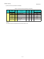
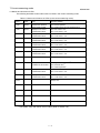
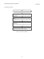
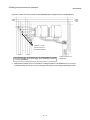
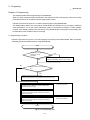
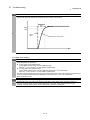
1
Energy Measuring Module User’s Manual (Details) MODEL QE83WH4W Thank you for purchasing the Mitsubishi MELSEC-Q series programmable controllers. Before using this product, please read this manual carefully and pay full attention to safety to handle the product correctly. Mitsubishi Programmable Controller C MODEL QE83WH4W-U-SY-E MODEL 19H866 CODE IB63722 2012 MITSUBISHI ELECTRIC CORPORATION IB63722 ● SAFETY PRECAUTIONS ● (Read these precautions before using this product.) This manual contains important instructions for MELSEC-Q series QE83WH4W. Before using this product, please read this manual and the relevant manuals carefully and pay full attention to safety to handle the product correctly. The precautions given in this manual are concerned with this product only. For the safety precautions of the programmable controller system, refer to the user’s manual of the CPU module used. In this manual, the safety precautions are classified into two levels: "DANGER" and "CAUTION". DANGER Indicates that incorrect handling may cause hazardous conditions, resulting in death or severe injury. CAUTION Indicates that incorrect handling may cause hazardous conditions, resulting in medium or slight personal injury or physical damage. Under some circumstances, failure to observe the precautions given under “ CAUTION” may lead to serious consequences. Observe the precautions of both levels because they are important for personal and system safety. Keep this manual in an accessible place for future reference whenever needed, and make sure it is delivered to the end user. [Precautions for Operating Environment and Conditions] CAUTION Do not use this product in the places listed below. Failure to follow the instruction may cause malfunctions or decrease of product-life. - Places the Ambient temperature exceeds the range 0 - 55ºC. - Places the Relative humidity exceeds the range 5 - 95% or condensation is observed. - Altitude exceeds 2000 m. - Places exposed to rain or water drop. - Dust, corrosive gas, saline and oil smoke exist. - Vibration and impact exceed the specifications. - Installation on excluding the control board [Design Precautions] DANGER Do not write data into “System Area” in the buffer memory of the intelligent function module. Also, do not output (turn ON) the “use prohibited” signal in the output signal sent from the sequencer CPU to the intelligent function module. Doing so may cause a malfunction to the sequencer system. A-1 CAUTION Do not install the input signal wire together with the main circuit lines or power cables. Keep a distance as below. (Except for the terminal input part) Failure to do so may result in malfunction due to noise. Conditions Distance Below 600V, or 600A power lines 300mm or more Other power lines 600mm or more [Installation Precautions] CAUTION Any person who is involved in the installation and the wiring of this Sequencer should be fully competent to do the work. Use the programmable controller in an environment that meets the general specifications in the User’s manual of the CPU module used. Failure to do so may result in electric shock, fire, malfunction, or damage to or deterioration of the product. To mount the module, while pressing the module-mounting lever located in the lower part of the module, fully insert the module fixing projection(s) into the hole(s) in the base unit and press the module until it snaps into place. Incorrect mounting may cause a malfunction, failure or a fall of the module. When using the Sequencer in an environment of frequent vibrations, fix the module with a screw. Tighten the screws within the specified torque range. Fixing-Module screw (arranged by user): M3 x 12mm Tightening torque of the fixing-module screws 0.36 - 0.48 N•m When the screw tightening is loose, it causes a fall, short-circuit, and a malfunction. Over-tightening can damage the screws and the module, and it may cause a fall, short-circuit, or a malfunction. Shut off the external power supply for the system in all phases before mounting or removing the module. Failure to do so may result in damage to the product. Do not touch directly any conductive parts and electronic parts of the module. Doing so can cause a malfunction or failure of the module. [Wiring Precautions] DANGER For installation and wiring works, make sure that the power source is shut off for all outside phases. If all phases are not turned off, it may cause an electric shock or product damages. When the input voltage of voltage transform unit is 55V or less, voltage display will be 0V by cut-off. The voltage maybe still applied even if the display is 0V. Touching the active wire is strictly prohibited. Make sure shut off the switch, and check the voltage was not been applied. A-2 CAUTION When using this product, make sure to use it in combination with current sensor (EMU-CT□□□ series or EMU2-CT5-4W) and Voltage transform unit (QE8WH4VT). Please not to exceed the ratings of this product for input of current sensor. For further details, please refer to current sensor manual to maintain the functionality and the accuracy of this product. The available range of the voltage transform unit is from 63.5/110 to 277/480V AC. When used in a circuit more than 227/480V AC, voltage transformer is required. Current sensor (EMU-CT50, EMU-CT100, EMU-CT250, EMU-CT400, EMU-CT600) is used only for low voltage circuit. It cannot be used with a high voltage circuit. Also, EMU2-CT5-4W should be used with the secondary side (5 A) of transformer transfixed. If it is connected with a high-voltage circuit by mistake, it may cause a burnout of the device and a fire. It is critically dangerous. For the Allowable maximum voltage, refer to Appendix 2 “Option devices”. Current sensor has a polarity (directionality). Be careful about it when installing the module. Do not open the secondary side of current sensor. Take care not entering any foreign objects such as chips and wire pieces into the module. It may cause a fire, failure or a malfunction. In order to prevent the module from incoming foreign objects such as wire pieces during wiring work, a foreign-object preventive label is placed on the module. While a wiring work is performed, keep the label on the module. Before operating the system, peel off the label for heat release. If the foreign-object preventive label is not peeled and the system is in use, residual heat inside the module may reduce the product life. The wires to be connected to the module shall be put in a duct or fixed together by clamp. If not, the loosing and unstable wire or careless stretching results in poor contact of electric wires. That may cause a breakage of the module or wire or a malfunction. After wiring, confirm whether there is a wiring forgetting or a faulty wiring. They may cause a device malfunction, a fire, or an electric shock. When removing the wires connected to the module, do not pull wires as holding on their electric wire portions. Push the buttons on the terminal, and then remove the wire. If the wires connected to the module are strongly pulled off, it may cause a malfunction or a breakage to the module or the wire. (Tensile load: 22N or less) Ensure the wiring to the module properly, checking the rated voltage and current of the product and the terminal pin assignment. If the input voltage exceed the rated voltage or the wiring is improper, it may cause a fire or a breakage. Do not exceed the specified voltage when doing an insulation resistance test and a commercial frequency withstand voltage test. To protect persons who do not have adequate knowledge of electric equipment from elevtric shocks, any of the following measures should be taken for the panel. (a) To lock the panel so that only trained persons having adequate knowledge of electric equipment can open it. (b) To design the structure so that the power is automatically interrupted upon opening of the panel. The protection class of the panel should be IP2X or higher. Terminal screws must be tightened to the specified torque. ( P8-1) Loose terminal screws may cause a short circuit or malfunction. If terminal screws are over-tightened, the screws or the module may be damaged, causing a short circuit or malfunction. Use an applicable solderless terminal for the current input line and tighten it to the specified torque. P8-8) If a spade terminal is used, it may fall, causing a breakage of the module when the terminal ( screw is loosened. Use appropriate size of electric wires. If inappropriate size of electric wire is used, it may cause a fire due to generated heat. For appropriate size of electric wires, refer to Section 8.5.2 How to connect P8-8). wires ( In case using stranded wire, take measures so that the filament should not vary by processing the point twisted. A-3 [Start-up Precautions] CAUTION Use the product within the ratings specified in this manual. When using it outside the ratings, it not only causes a malfunction or failure but also there is a fear of igniting and damaging by a fire. Before operating the product, check that active bare wire and so on does not exist around the product. If any bare wire exists, stop the operation immediately, and take an appropriate action such as isolation protection. Do not disassemble or modify the module. It may cause failure, a malfunction, an injury or a fire. Attaching and detaching the module must be performed after the power source is shut off for all outside phases. If not all phases are shut off, it may cause failure or a malfunction of the module. Do not touch the live terminal. It may cause a malfunction. [Maintenance Precautions] CAUTION Cleaning and additional tightening of screws must be performed after the input power source is shut off for all outside phases. If not all phases are shut off, it may cause failure or a malfunction of the module. Use a soft dry cloth to clean off dirt of the module surface. Do not let a chemical cloth remain on the surface for an extended period nor wipe the surface with thinner or benzene. Check for the following items for using this product properly for long time. <Daily maintenance> (1) No damage on this product (2) No abnormality with LED indicators (3) No abnormal noise, smell or heat. <Periodical maintenance> (Once every 6 months to 1 year) (4) Confirm there is loosing in installation, wire connection to terminal blocks, and the connection of the connectors. (Check these items under the power failure condition.) [Storage Precautions] CAUTION To store this product, turn off the power and remove wires, and put it in a plastic bag. For long-time storage, avoid the following places. Failure to follow the instruction may cause a failure and reduced life of the product. - Places the Ambient temperature exceeds the range -25 to +75ºC. - Places the Relative humidity exceeds the range 5 - 95% or condensation is observed. - Dust, corrosive gas, saline and oil smoke exist, and vibration and frequent physical impact occur. - Places exposed to rain or water drop. [Disposal Precautions] CAUTION Dispose of the product as an industrial waste. A-4 Revision history * Instruction Manual Number is provided at the bottom of the cover page. Printed date *Instruction Manual # July, 2012 IB-63722 Description of revisions First edition This manual does not guarantee to protect or does not give permission to any industrial property and any related rights. Also, our company shall not be held any responsible for any issues related to industrial properties due to product usage described in this manual. 2012 MITSUBISHI ELECTRIC CORPORATION A-5 Table of Content Safety precautions············································································································································A-1 Revision history ················································································································································A-5 Table of content················································································································································A-6 Compliance with the EMC and Low Voltage Directives··················································································A-8 Product configuration ·······································································································································A-8 Chapter 1: Overview 1-1 1.1 Features ····················································································································································· 1-1 Chapter 2: System Configuration 2-1 - 2-4 2.1 Applicable system ······································································································································ 2-1 2.2 How to check the function version, serial number, and module version ·················································· 2-3 Chapter 3: Specifications 3-1 - 3-3 3.1 General specifications ······························································································································ 3-1 3.2 Electrical and mechanical specifications ··································································································· 3-2 Chapter 4: Functions 4-1 - 4-15 4.1 List of functions··········································································································································· 4-1 4.2 Functions in detail ····································································································································· 4-2 Chapter 5: I/O signal to CPU module 5-1 - 5-7 5.1 List of I/O signals········································································································································ 5-1 5.2 Details of I/O signals ·································································································································· 5-2 Chapter 6: Buffer memory 6-1 - 6-29 6.1 Buffer memory assignment························································································································ 6-1 6.2 Configurable sections (Un\G0 to Un\G99)······························································································· 6-6 6.3 Measurement sections (Un\G100 to Un\G2999)··················································································· 6-14 6.4 Common sections (Un\4500 to Un\G4999) ··························································································· 6-29 Chapter 7: Current measuring mode 7-1 - 7-6 7.1 Measuring functions in the current measuring mode················································································ 7-1 7.2 Activating the current measuring mode ··································································································· 7-1 7.3 List of I/O signals········································································································································ 7-2 7.4 Buffer memory············································································································································ 7-3 7.5 Names and functions of LEDs ··················································································································· 7-4 7.6 Names of signals of terminal block············································································································ 7-5 7.7 Wiring·························································································································································· 7-6 A-6 Chapter 8: Setting and procedure for operation 8-1 - 8-20 8.1 Precautions for handling ·························································································································· 8-1 8.2 Procedure for operation ··························································································································· 8-2 8.3 Name and function of each part················································································································· 8-3 8.4 Attaching and removing the module ········································································································ 8-6 8.5 Wiring ························································································································································ 8-7 8.6 Setting from GX Developer ···················································································································· 8-16 Chapter 9: Programming 9-1 - 9-16 9.1 Programming procedure ·························································································································· 9-1 9.2 System configuration and usage conditions for sample program ··························································· 9-2 9.3 System configuration and usage conditions for current measuring mode ··············································· 9-9 Chapter 10: Troubleshooting 10-1 - 10-9 10.1 List of error codes ································································································································· 10-1 10.2 Troubleshooting ····································································································································· 10-3 10.3 Q&A ······················································································································································ 10-6 Appendix Appendix 1 - 6 Appendix 1: External dimensions ·······································································································Appendix-1 Appendix 2: Optional devices ·············································································································Appendix-2 Index Index 1 A-7 Compliance with the EMC and Low Voltage Directives (1) For programmable controller system To configure a system meeting the requirements of the EMC and Low Voltage Directives when incorporating the Mitsubishi programmable controller (EMC and Low Voltage Directives compliant) into other machinery or equipment, refer to Chapter 9 "EMC AND LOW VOLTAGE DIRECTIVES" of the QCPU User's Manual (Hardware Design, Maintenance and Inspection). The CE mark, indicating compliance with the EMC and Low Voltage Directives, is printed on the rating plate of the programmable controller. (2) For the product For the compliance of this product with the EMC and Low Voltage Directives, refer to Section 8.5 Wiring. (3) CE marking conformity combination module This module conforms to CE marking standard in a condition to make combination use with following current censor and cable. (a)Current input EMU-CT50,EMU-CT100, current censor EMU-CT250,EMU-CT400, EMU2-CT5-4W EMU-CT600 EMU2-CB-Q5B-4W CE marking cable (twisted pair cable) EMU2-T1M, EMU2-T5M cable or Stranded wire: 1.3 mm2 (0.5 - 1.3 mm2) current censor cable EMU2-T10M, EMU2-T1MS Solderless terminal: R1.25-3 EMU2-T5MS, EMU2-T10MS Max. cable length 50m 11m (b)Voltage input cable Max. cable length CE marking cable (twisted pair cable) Single wire: φ1.2 mm (φ0.5 - 1.2 mm) Stranded wire: 1.3 mm2 (0.5 - 1.3 mm2) 50m Product configuration The following describes the product configuration. Model name QE83WH4W Product name Quantity Energy Measuring Module 1 Voltage input terminals 1 A-8 Note A-9 1 Overview QE83WH4W Chapter 1: Overview This manual explains specifications, handling methods, and programming of Energy Measuring Module QE83WH4W (hereinafter, abbreviated as QE83WH4W) supporting MELSEC-Q series. 1.1 Features (1) This Energy Measuring Module can measure three channels of various types of electric quantity. It can measure three channels of electric energy, reactive energy, current, voltage, electric power, reactive power, power factor, and frequency. Both consumption and regeneration of the electric energy can be measured. (2) Extensive monitoring functions In addition to memorizing the maximum and minimum values, two types of alarm monitoring for upper and lower limit can be performed for each channel. (3) It also can measure the electric energy for a certain period. It can measure the electric energy for the duration of time for which the output device is on. This feature enables to acquire the electric energy needed during device operation or energy per tact. (4) Equipped with the current measuring mode where eight channels of current can be measured. By selecting the current measuring mode using the intelligent function module switch, you can measure only the current through eight channels. Note that the input/output signals and buffer memory to be used in the current measuring mode are different from those used in the regular operation mode. For details, refer to Chapter 7. 1-1 2 System configuration QE83WH4W Chapter 2: System Configuration 2.1 Applicable system The following describes applicable systems. (1) Applicable module and the quantity of attachable pieces (a)When mounted with CPU module CPU module to which QE83WH4W can be attached and the number of attachable pieces are shown below. Depending on the combination of the attached module and the number of attached pieces, lack of power capacity may occur. When attaching the module, please consider the power capacity. If the power capacity is insufficient, reconsider the combination of modules to be attached. Since the number of attachable modules are limited by the power module which used, please refer to the notes on the 2.2 precautions for system configuration. Remarks Number of Applicable CPU Module CPU Type Programmable controller CPU CPU Model Q00JCPU Basic model Q00CPU QCPU Q01CPU Q02CPU Q02HCPU High performance Q06HCPU model QCPU Q12HCPU Q25HCPU Q02PHCPU Q06PHCPU Process CPU Q12PHCPU Q25PHCPU Q12PRHCPU Redundant CPU Q25PRHCPU Q00UJCPU Q00UCPU Q01UCPU Q02UCPU Q03UDCPU Q04UDHCPU Q06UDHCPU Q10UDHCPU Q13UDHCPU Universal model Q20UDHCPU QCPU Q26UDHCPU Q03UDECPU Q04UDEHCPU Q06UDEHCPU Q10UDEHCPU Q13UDEHCPU Q20UDEHCPU Q26UDEHCPU Q50UDEHCPU Q100UDEHCPU 2-1 modules 8 24 64 64 53 8 24 36 64 2 System configuration QE83WH4W Applicable CPU Module CPU Type Number of CPU Model Q06CCPU-V Q06CCPU-V-B Q12DCCPU-V C Controller module Remarks modules 64 (b) When mounted with MELSECNET/H remote I/O station The table below shows the network modules applicable to the QE83WH4W and the number of network modules to be mounted. Depending on the combination with other modules or the number of mounted modules, power supply capacity may be insufficient. Pay attention to the power supply capacity before mounting modules, and if the power supply capacity is insufficient, change the combination of the modules. Remarks Number of modules Applicable Network Module QJ72LP25-25 QJ72LP25G QJ72BR15 64 (c) The base unit can be mounted QE83WH4W can be installed to any I/O slot of main base unit and extension base unit. *1 In case of redundant CPU, can be mounted to the extension base unit only. Mounted to the main base unit is not allowed. *2 Limited within the range of I/O points for the CPU module. (2) Attachable base unit QE83WH4W can be attached to any I/O slot of the basic base unit and expansion base unit (*1) (*2). *1 In the case of dual CPU, it can be attached only to an expansion base unit. It cannot be attached to the base unit. *2 It has to be within the range of I/O slots of the CPU module. (3) Applicable software package QE83WH4W supported software packages are as follows: (a) Software package for sequencer Product name Model name GX Works2 Remarks SW1DNC-GXW2 Sequencer engineering software MELSEC sequencer programming software GX Developer SWnD5C-GPPW “n” in the model name is 4 or larger. 2-2 2 System configuration QE83WH4W 2.2 How to check the function version, serial number, and module version (1) How to check the module version It can be checked with the serial number label (placed on the right side of QE83WH4W). Module version 19H013 710A1234 Serial number Barcode (2) How to check the function version and serial number (a) Checking on the front of the module The serial number and function version on the rating plate is shown on the front (at the bottom) of the module. Function version Serial number 2-3 2 System configuration QE83WH4W (b) Checking on the System monitor dialog box (Product Information List) To display the system monitor, select [Diagnostics] → [System monitor] and click the Product Information List button of GX Developer. Point The serial number displayed on the Product Information List dialog box of GX Developer may differ from that on the rating plate and on the front of the module. ・ The serial number on the rating plate and front part of the module indicates the management information of the product. ・ The serial number displayed on the Product Information List dialog box of GX Developer indicates the function information of the product. The function information of the product is updated when a new function is added. 2-4 3 Specifications QE81WH4W Chapter 3: Specifications 3.1 General specifications Rating Item Phase wire system Voltage circuit *1 Current circuit Frequency Allowable tolerance of main module (excluding current sensor) *3 Measurable circuit count Data update cycle Response time Backup for electric blackout I/O occupation Specifications three-phase 4-wire 63.5/110 - 277/480V AC (Selected from: 63.5/110V,100/173V,105/182V,110/190V,115/199V, 120/208V,127/220V,200/346V,220/380V,230/400V,240/415V,242/420V, 250/430V,254/440V,265/460V,277/480V AC. Each value refers to the primary voltage of voltage transform unit (QE8WH4VT).) 50 A, 100 A, 250 A, 400 A, 600 A AC (Current sensor is used. Each value refers to the current at the primary side of current sensor.) 5 A AC (Current sensor is used together with current transformer (CT), and the primary-side current is configurable up to 6000 A.) *2 50-60 Hz Current, current demand *4 : ±1.0% (100% of the rating) Voltage : ±1.0% (100% of the rating) Electric power, electric power demand : ±1.0% (100% of the rating) Reactive power : ±1.0% (100% of the rating) Apparent power : ±1.0% (100% of the rating) Frequency : ±1.0% (45 – 65 Hz range of the rating) Power factor : ±3.0% (against the electric angle 90°) Electric energy : ±2.0% (5 – 100% range of the rating, power factor = 1) Reactive energy : ±2.5% (10 – 100% range of the rating, power factor = 0) 3 circuits (3 channels) under the same voltage system, or 8 circuits (8 channels) in the current measuring mode *5 500 ms (100 ms in the current measuring mode) 2 seconds or less Backup is made using nonvolatile memory. (Stored items: settings, the max./min. values and time of occurrence, electric energy (consumption, regenerated), reactive energy (consumption lag), and periodic electric energy) 32 points (I/O assignment: intelligence 32 points) * 1:Voltage input is required a voltage transform unit (QE8WH4VT). Above 277/480V AC voltage transformer outside (VT) is required (Primary side of VT can be set up to 6600V (phase voltage) in any setting). * 2:5 A primary current can be set when using the current sensor is as follows. 5A, 6A, 7.5A, 8A, 10A, 12A, 15A, 20A, 25A, 30A, 40A, 50A, 60A, 75A, 80A, 100A, 120A, 150A, 200A, 250A, 300A, 400A, 500A, 600A, 750A , 800A, 1000A, 1200A, 1500A, 1600A, 2000A, 2500A, 3000A, 4000A, 5000A, 6000A (Primary current of CT can be set up to 6000A in any . However, secondary current of CT can not be set to other than 5A). * 3:The ratio error of the current sensor : ±1.0% (5 – 100% range of the rating), and the ratio error of voltage transform unit : ±1.0% (primary voltage of the rating) * 4:Demand shows the moving average of a set period. * 5 : Always accumulating the integrated values of Wh and varh. It can capture short-cycled load fluctuation(500 ms or shorter). 3-1 3 Specifications QE81WH4W 3.2 Electrical and mechanical specifications Item Consumed VA Voltage circuit Current circuit Internal current consumption (5 V DC) Operating temperature Operating humidity Storage temperature Storage humidity Operating altitude Installation area Operating environment Vibration resistance Specifications P1-P0: 2VA, P2-P0: 0.3VA, P3-P0: 0.3VA (primary side of voltage transform unit) Each phase 0.1 VA (secondary side of current sensor) 0.39 A 0 – 55°C (Average daily temperature 35°C or below) 5 – 95% RH (No condensation) -25° – +75°C 5 – 95% RH (No condensation) 2000m or below Inside a control panel No corrosive gas Frequency Constant Conforms acceleration to JIS B Intermittent 5 – 8.4 Hz 3502, IEC vibration 61131-2 8.4 – 150 Hz 9.8 m/s2 Continuous vibration Impact resistance 1 Over voltage category * 2 Pollution degree * Equipment category Applicable Voltage input wire terminal (Usable Current input 3 electric terminal * 6 wire) * Tightening torque Commercial frequency withstand voltage 5 – 8.4 Hz 8.4 – 150 Hz 4.9 m/s2 Half amplitude 3.5 mm - 1.75 mm - Sweep time XYZ each direction 10 times - 2 Conforms to JIS B 3502, IEC 61131-2 (147m/s , XYZ each direction 3 times) II or less 2 or less Class Ι Tightening torque : 0.4 – 0.5 N・m Single wire AWG24-16 4 Stranded wire * AWG20-16 4 Stranded wire * AWG20-18 Applicable solderless terminals : R1.25-3 (No solderless terminal with insulation sleeve can be used) Tightening torque : 0.42 – 0.58 N・m Current input terminal block fixing 0.66 - 0.89 Nm screws (M3.5) 5 Module-fixing screws (M3 screw) * 0.36 – 0.48 N▪m Between voltage/current input terminals - SLD terminal 2210 V AC 5 sec 2210 V AC 5 sec Between voltage/current input terminals - sequencer power source and GND terminals Insulation resistance 5 MΩ or more (500 V DC) at locations above Standard EMC: EN61131-2:2007, EN61326-1:2006 LVD: EN61131-2:2007, EN61010-1:2001 Dimensions 27.4 mm (W) x 98 mm (H) x 112mm (D) excluding protruding portions Mass 0.19kg Product life expectancy 10 years (used under the average daily temperature 35°C or less) *1. This indicates the assumed area of electric distribution to which the device is connected, the area ranging from public distribution to factory machinery. The category II applies to the device power-supplied from fixed facility. The surge voltage of this product is 2500 V up to the rated voltage of 300 V. *2. The index indicates the level of conductive substance at the device’s operating environment. Contamination level 2 means only non-conductive substance. However, occasional condensation may lead to temporary conduction. *3. At the connection between the secondary terminal of current sensor (k, l) and the main module terminal (1k, 1l, 2k, 2l, 3k, 3l), use twisted pair cable. 3-2 3 Specifications QE81WH4W *4. When using stranded wires for the voltage input terminals, use solderless terminals or strand the wire edges to prevent thin wires from loosening. *5. When using stranded wires for the current input terminals, use applicable solderless terminals. If any spade solderless terminal is used, it may be disconnected when the terminal screw comes loose, resulting in failure. In addition, no solderless terminal with insulation sleeve can be used. *6. The module can be fixed easily to the base unit, using the hook on top of the module. However, if it is used under a vibrating environment, we strongly recommend that the module be fixed with screws. *7. To comply with UL/c-UL standards, use the wires meeting the following requirements. The rated temperature of the copper conductor should be 60ºC/75ºC. 3-3 4 Functions QE83WH4W Chapter 4: Functions 4.1 List of functions Functions of QE83WH4W are provided in Table 4.1. The “n” that is used in this and later chapters (for example: Xn0, Yn0, Un\G0, etc.) refers to the number that appears at the beginning of QE83WH4W. Table 4.1 List of Functions No. Function Descriptions Reference section It measures current, current demand, voltage (L-L), voltage (L-N), electric power, reactive power, apparent 1 Measurement power, electric power demand, power factor, frequency, Section effective energy (consumption, regeneration), reactive 4.2.1 energy (consumption lag), and sequentially stores the records into a buffer memory. The electric energy only for a period of time when a 2 Periodic electric certain output signal is ON will be stored in the buffer energy memory. Section 4.2.2 Periodic energy 1 and 2 can be measured independently. 3 Hold max./min. values For current demand, line voltage, phase voltage, electric power demand, and power factor, each maximum /minimum values and date/time of occurrence are stored. Section 4.2.3 Of current demand, line voltage, phase voltage, electric 4 Upper/lower limit alarm monitoring power demand, and power factor, you can select two items for which their upper/lower limit can be monitored. If it exceeds the upper limit or goes below the lower limit, Section 4.2.4 the specified input signal is turned on. Selecting the test mode using the intelligent function module switch enables pseudo-storage of the specified value into 5 Test the buffer memory, even with non-existence of input from voltage and current (sensor). Section 4.2.5 Using this module, you can create a sequence, etc. 6 Integrated value setting Setting integrated value ( electric energy ( consumption, regeneration ) and reactive energy (consumption lag) ) to any value. Section 4.2.6 By selecting the current measuring mode using the 7 Current measuring intelligent function module switch, you can measure eight mode function channels of current and sequentially store the records into the buffer memory. 4-1 Chapter 7 4 Functions QE83WH4W 4.2 Functions in detail 4.2.1 Measuring functions (1) Measured items Measured items of each channel are described as follows: Each measured item is stored in the buffer memory every 500 ms. Measured items Details Current Current demand * The average of fluctuation for the set period of current demand time is indicated. Voltage Electric power Electric power demand * The average of fluctuation for the set period of electric power demand time is indicated. Reactive power Apparent power 1 - phase current 2 - phase current 3 - phase current Neutral current Average value current 1 - phase current demand 2 - phase current demand 3 - phase current demand Neutral current demand Max. value Min. value Date of max. value occurrence Date of min. value occurrence Voltage V12 Voltage V23 Voltage V31 average value voltage (L-L) Max. value of the voltage (L-L) Min. value of the voltage (L-L) Date/time of max. voltage value occurrence (L-L) Date/time of min. voltage value occurrence (L-L) Voltage V1N Voltage V2N Voltage V3N average value voltage (L-N) Max. value of the voltage (L-N) Min. value of the voltage (L-N) Date/time of max. voltage value occurrence (L-N) Date/time of min. voltage value occurrence (L-N) Present value Present value Max. value Min. value Date/time of max. value occurrence Date/time of min. value occurrence Reactive power Apparent power 4-2 4 Functions QE83WH4W Present value Max. value Min. value Date/time of max. value occurrence Date/time of min. value occurrence Frequency Present value Electric energy Electric energy (consumption) Electric energy (regeneration) Reactive energy (consumption lag) Periodic electric energy *2 Periodic electric energy 1 Periodic electric energy 2 *2: When the output device is ON, the active power (consumption) is measured. Power factor (2) Total, maximum, and minimum values Item The following describes how to calculate the maximum, minimum, and total values. Formula Average value current Average value current = (1-phase current + 2-phase current + 3-phase current) / 3 Average value voltage (L-L) Average value voltage (L-L) = (voltage V12 + voltage V23 + voltage V31) / 3 Average value voltage (L-N) Average value voltage (L-N) = (voltage V1N + voltage V2N + voltage V3N) / 3 Maximum current demand Maximum value voltage (L-L) Highest value among 1-phase current demand, 2-phase current demand, 3-phase current demand, or N-phase current demand (The highest value after the max./min. value was reset.) Lowest value among 1-phase current demand, 2-phase current demand, or 3-phase current demand (The lowest value after the max./min. value was reset.) Highest value among the voltage V12, the voltage V23, or the voltage V31 (The highest value after the max./min. value was reset.) Minimum value voltage (L-L) Lowest value among the voltage V12, the voltage V23, or the voltage V31 (The lowest value after the max./min. value was reset.) Maximum value voltage (L-N) Highest value among the voltage V1N, the voltage V2N, or the voltage V1N (The highest value after the max./min. value was reset.) Minimum value voltage (L-N) Lowest value among the voltage V1N, the voltage V2N, or the voltage V1N (The highest value after the max./min. value was reset.) Minimum current demand 4-3 4 Functions QE83WH4W (3) Resolution of measured data Resolution of measured data according to the rating (phase wire system, primary voltage, and primary current) is described as follows. 1) Current, current demand Rated primary current setting Multiplier 5 A to 30 A -3 40 A to 300 A -3 400 A to 3000 A 4000 A to 6000 A -3 -3 Resolution* 2 digits after the decimal point 1 digit after the decimal point Integer ×10 0.01 A 0.1 A 1A 10 A * Digits lower than the resolution are fixed to 0. 2) Voltage a. When not use voltage transformer Input voltage setting Multiplier 63.5 / 110 V to 277 / 480 V -3 b. When use voltage transformer Rated primary voltage setting Multiplier 1 V to 329 V -3 330 V to 2299 V -3 3300 V to 6600 V -3 * Digits lower than the resolution are fixed to 0. Resolution* 1 digit after the decimal point 0.1 V Resolution* 1 digit after the decimal point Integer ×10 0.1 V 1V 10 V 3) Electric power, electric power demand, reactive power, apparent power Full load power W*1*3 Multiplier Resolution*2*3 Ⅰ. Ⅱ. -3 W <12 kW 12 kW ≤ W < 120 kW -3 Ⅲ. 120 kW ≤ W < 1200 kW -3 3 digits after the decimal point 2 digits after the decimal point 1 digit after the decimal point Integer ×10 0.001 kW 0.01 kW 0.1 kW -3 1 kW Ⅳ. 1200 kW ≤ W < 12000 kW -3 10 kW Ⅴ.12000 kW ≤ W < 120000 kW *1 Full load power W can be calculated by the following equation: In addition, for calculating full load power W, refer to Table 4.2. Full load power W [kW] = 3×(VT primary voltage)×(CT primary current) / 1000 Primary voltage = voltage (L-N) of input voltage (when not use voltage transformer) = primary voltage of voltage transformer (when use voltage transformer) *2 Digits lower than the resolution are fixed to 0. *3 In the case of reactive power, the unit will be kvar. In the case of apparent power, the unit will be kVA 4) Power factor Power factor Multiplier All setting ranges -3 * Digits lower than the resolution are fixed to 0. 4-4 Resolution* 1 digit after the decimal point 0.1% 4 Functions QE83WH4W 5) Frequency Frequency Multiplier All setting ranges Resolution* 1 digit after the decimal point -3 0.1 Hz * Digits lower than the resolution are fixed to 0. 6) Electric energy, periodic electric energy Full load power Multiplier W*1 Ⅰ. W< 12 kW Ⅱ. 12kW ≤ W < 120 kW Ⅲ. 120kW ≤ W < 1200 kW Ⅳ. 1200kW ≤ W < 12000 kW Ⅴ.12000kW ≤ W < 120000 kW Resolution*2*3 Range [kWh,kvarh] 5 digits after the decimal point 4 digits after the decimal point 3 digits after the decimal point 2 digits after the decimal point 1 digit after the decimal point -5 -4 -3 -2 -1 0.00001 – 9999.99999 0.0001 – 99999.9999 0.001 – 999999.999 0.01 – 9999999.99 0.1 – 99999999.9 *1 For calculating full load power W, refer to Table 4.2. Digits lower than the resolution are fixed to 0. *3 Because the higher resolution than a typical watt-hour meter, the minimum digit values will change more than 2 at once update. According to setting value of input voltage, primary current, primary voltage of VT and the condition of load. *2 Table 4.2 How to calculate full load power Primary voltage [V] Primary current[A] Ⅰ W<12kW Ⅱ 12kW≦W<120kW Ⅲ 120kW≦W<1200kW Ⅳ 1200kW≦W<12000kW Ⅴ 12000kW≦W<120000kW 4-5 ~ ~ ~ ~ ~ ~ ~ ~ ~ ~ ~ ~ ~ ~ ~ ~ ~ ~ ~ 79 99 133 159 199 266 333 399 499 533 666 799 999 1333 1559 1999 2666 3333 3999 4999 5333 6600 ~ 66 ~ 5 6 7.5 8 10 12 15 20 25 30 40 50 60 75 80 100 120 150 200 250 300 400 500 600 750 800 1000 1200 1500 1600 2000 2500 3000 4000 5000 6000 ~ 67 80 100 134 160 200 267 334 400 500 534 667 800 1000 1334 1600 2000 2667 3334 4000 5000 5334 ~ 63.5 4 Functions QE83WH4W (4) Restrictions for measuring data - Measurement cannot be performed immediately after the power loading to the sequencer system (Module ready signal is under the OFF condition). After checking that Module ready (Xn0) is ON, obtain measuring data. - Measurement cannot be performed immediately after operating conditions are set up to the module. After checking that Operating condition setting completion flag (Xn9) becomes ON, obtain measuring data. - Behaviors during operation are as follows: Measuring item Current Current demand Voltage (L-N) Voltage (L-L) Electric power Electric power demand Power factor Frequency Behavior of the module When the input current is less than 0.4% of the rating current, it becomes 0A. Current demand is obtained by current moving average. Therefore, even if current is 0A, current demand may not be 0A. When the input voltage (L-N) is less than 55V, it becomes 0V. If there is no input at voltage V1N, all measurement cannot be done. When the input voltage (L-L) is less than 95V, it becomes 0V. When current is 0A (at all phases are 0A) or when voltage is 0V (all phases are 0V), it becomes 0kW. Electric power demand is obtained by electric power moving average. Therefore, even if electric power is 0kW, electric power demand may not be 0kW. When current is 0A (at all phases are 0A) or when voltage is 0V (all phases are 0V), it becomes 100%. Voltage condition When the input voltage (L-N) is less than 55V, it becomes 0Hz. Frequency condition When it is less than 44.5Hz, it is fixed to 44.5Hz. 4-6 4 Functions QE83WH4W 4.2.2 Measuring function for periodic electric energy This function is to measure electric energy for a certain period, and stores it into the buffer memory. It can be used to measure electric energy for a certain tact or energy (standby power) when the facility or equipment is not in operation. (1) Overview 1) It can measure two periodic electric energy (periodic electric energy 1 and periodic electric energy 2) of each channel. Each of these can be measured independently. 2) During the time when Periodic electric energy 1 measurement flag / Periodic electric energy 2 measurement flag is ON, periodic electric energy can be measured. 3) Periodic electric energy is stored in the nonvolatile memory, so that it can be retained even at a power source reset. 4) I/O signals and buffer memory corresponding to each periodic electric energy 1 and 2 are provided below. Periodic electric energy measuremen t flag Periodic electric energy data completion flag Periodic electric energy reset request Periodic electric energy reset completion flag Un\G114, 115 Yn5 Xn5 Yn7 Xn7 Un\G116, 117 Yn6 Xn6 Yn8 Xn8 Un\G1114, 1115 YnB XnB YnD XnD Un\G1116, 1117 YnC XnC YnE XnE Un\G2114, 2115 Yn11 Xn11 Yn13 Xn13 Un\G2116, 2117 Yn12 Xn12 Yn14 Xn14 Buffer memory (Double words) Periodic electric CH1 energy 1 Periodic electric energy 2 Periodic electric CH2 energy 1 Periodic electric energy 2 Periodic electric CH3 energy 1 Periodic electric energy 2 Note Measurement of periodic electric energy is performed every measuring cycle (500 ms). Therefore, if the time to turn ON the periodic electric energy measurement flag is set to 500 ms or less, measurement may not be taken. 4-7 4 Functions QE83WH4W (2) Basic procedure 1) Measuring periodic electric energy (a) Check that CH1 periodic electric energy 1 measurement flag (Yn5) is OFF. (b) Check CH1 periodic electric energy 1 (Un\G114, 115). (c) When starting measurement, set CH1 periodic electric energy 1 measurement flag (Yn5) to ON. This module starts measuring the specified periodic electric energy, and CH1 periodic electric energy 1 data completion flag (Xn5) will be turned OFF (d) When stopping measurement, set CH1 periodic electric energy 1 measurement flag (Yn5) to OFF. This module stops measuring the specified periodic electric energy, and CH1 periodic electric energy 1 data completion flag (Xn5) will be turned ON. (e) Check that CH1 periodic electric energy 1 data completion flag (Xn5) becomes ON, and obtain the value of periodic electric energy. CH1 periodic electric energy 1 CH1 periodic electric energy 1 measurement flag (Yn5) CH1 periodic electric energy 1 data completion flag (Xn5) Figure 4.1 Basic procedure of measuring the periodic electric energy 2) Resetting periodic electric power (a) Check that CH1 periodic electric energy 1 measurement flag (Yn5) is OFF and CH1 periodic electric energy 1 reset request (Yn7) is OFF. (b) Set CH1 periodic electric energy 1 reset request (Yn7) to ON. The specified periodic electric energy is reset to 0 kWh, and CH1 periodic electric energy 1 reset completion flag (Xn7) will be turned ON. (c) Check that CH1 periodic electric energy 1 reset completion flag (Xn7) has become ON, and then set CH1 periodic electric energy 1 reset request (Yn7) to OFF. CH1 periodic electric energy 1 reset completion flag (Xn7) will be turned OFF. CH1 periodic electric energy 1 CH1 periodic electric energy 1 reset request (Yn7) CH1 periodic electric energy 1 reset completion flag (Xn7) Figure 4.2 How to reset the periodic electric energy 4-8 4 Functions QE83WH4W (3) Sample use case 1) Procedure for continuously measuring periodic electric energy If you turn CH1 periodic electric energy 1 measurement flag to ON only for the extent of time you want to measure, this module accumulates the power starting at the previously measured amount. Usage procedure is the same as 1) in (2). An example is provided below. CH1 periodic electric energy 1 CH1 periodic electric energy 1 measurement flag (Yn5) CH1 periodic electric energy 1 data completion flag (Xn5) Figure 4.3 Example of continuous measurement of periodic electric energy 2) Procedure for measuring periodic electric energy after every reset If you turn Periodic electric energy measurement flag (Yn1/Yn2) to ON only for the extent of time you want to measure, this module accumulates the power starting at the previously measured amount. The following describes the usage procedure. (a) Check that CH1 periodic electric energy 1 measurement flag (Yn5) is OFF and CH1 periodic electric energy 1 reset request (Yn7) is OFF. (b) Set CH1 periodic electric energy 1 reset request (Yn7) to ON. The specified periodic electric energy is reset to 0 kWh, and CH1 periodic electric energy 1 reset completion flag (Xn7) will be turned ON. (c) Check that CH1 periodic electric energy 1 reset completion flag (Xn7) has become ON, and then set CH1 periodic electric energy 1 reset request (Yn7) to OFF. CH1 periodic electric energy 1 reset completion flag (Xn7) will be turned OFF. (d) When starting measurement, set CH1 periodic electric energy 1 measurement flag (Yn5) to ON. This module starts measuring the specified periodic electric energy, and CH1 periodic electric energy 1 data completion flag (Xn5) will be turned OFF. (e) When stopping measurement, set CH1 periodic electric energy 1 measurement flag (Yn5) to OFF. This module stops measuring the specified periodic electric energy, and CH1 periodic electric energy 1 data completion flag (Xn5) will be turned ON. (f) Check that CH1 periodic electric energy 1 data completion flag (Xn5) becomes ON, and obtain the value of periodic electric energy. CH1 periodic electric energy 1 CH1 periodic electric energy 1 measurement flag (Yn5) CH1 periodic electric energy 1 data completion flag (Xn5) CH1 periodic electric energy 1 reset request (Yn7) CH1 periodic electric energy 1 reset completion flag (Xn7) Figure 4.4 Example of measurement of periodic electric energy after every reset 4-9 4 Functions QE83WH4W 4.2.3 Max./min. value hold function It memorizes the max./min. value for each measured item, and retains it until the max./min. value clear is performed. (1) Max./min. value memory 1) It memorizes the max. and min. values of the following measured items of each channel. - Current demand - Voltage - Electric power demand - Power factor 2) It memorizes the date and time of occurrence (year/month/day/hour/minute/second/day of the week) together with the max. and min. values. 3) The max. and min. values and the date of occurrence are stored in the nonvolatile memory, so that these values can be retained even at a power source reset. (2) How to clear the max. and min. values 1) You can use the I/O signal to clear the max. and min. values. 2) The max. and min. values immediately after the clear will be the present values and the date of occurrence will be the present date and time. 3) The following describes how to clear the max. and min. values. (a) Check that Max./min. values clear request (Yn4) is OFF. (b) In the max./min. value clear target (Un\G56), set the measured items of the channel you want to clear. (c) Set Max./min. values clear request (Yn4) to ON. This module clears the max./min. values of the measured items of the channel you selected in step (b) above and their date of occurrence and turns Max./min. values clear completion flag (Xn4) to ON. (d) Check that Max./min. values clear completion flag (Xn4) is ON, and then set Max./min. values clear request (Yn4) to OFF. Max./min. values clear completion flag (Xn4) will be turned OFF. Max./min. values clear request (Yn4) Max./min. values clear completion flag (Xn4) Figure 4.5 Procedure for clearing max./min. value 4 - 10 4 Functions QE83WH4W 4.2.4 Upper/lower limit alarm monitoring function You can set an upper and lower limit alarm for maximum two points for each channel and implement a monitoring function for them. During the alarm monitoring, it can monitor the input signal to check for the occurrence. (1) Setting the upper/lower limit alarm monitoring 1) Setting items and setting range for the alarm monitoring are described below. Items set in the buffer Setting range Description memory Alarm item 0: No monitoring For respective alarm 1 and alarm 2, 1: Current demand upper limit set the measuring item and either 2: Current demand lower limit upper or lower limit for monitoring 3: Voltage (L-L)upper limit target. 4: Voltage (L-L)lower limit 5: Power demand upper limit 6: Power demand lower limit 7: Power factor upper limit 8: Power factor lower limit 9: Voltage (L-N) upper limit 10: Voltage (L-N)lower limit The value to be monitored for the Alarm value -2147483648 – 2147483647 [Unit] Current:×10-3 A alarm. Set the value according to the Voltage:×10-3 V unit of the measuring item that is set Power:×10-3 kW as an alarm monitoring item. PF:×10-3% (Double words) Alarm reset method 0: Self-retention Set whether or not the 1: Auto reset alarm-occurrence condition should be retained if the value goes below the upper limit alarm value or goes over the lower limit alarm value after the upper/lower limit alarm occurred. Alarm delay time 0 – 300 If it exceeds the upper limit alarm [Unit] second value or if it goes below the lower limit alarm value, and the situation continues for the period of the alarm delay time, then it is considered as an alarm occurrence. The table below shows I/O signals and buffer memory for alarm 1 and alarm 2. Alarm reset Alarm flag request CH1 CH2 CH3 Buffer memory (Double words) Alarm item Alarm value Alarm reset Alarm method time Alarm 1 Yn9 Xn9 Un\G11 Un\G12, 13 Un\G14 Un\G15 Alarm 2 YnA XnA Un\G21 Un\G22, 23 Un\G24 Un\G25 delay Alarm 1 YnF XnF Un\G1011 Un\G1012, 1013 Un\G1014 Un\G1015 Alarm 2 Yn10 Xn10 Un\G1021 Un\G1022, 1023 Un\G1024 Un\G1025 Alarm 1 Yn15 Xn15 Un\G2011 Un\G2012, 2013 Un\G2014 Un\G2015 Alarm 2 Yn16 Xn16 Un\G2021 Un\G2022, 2023 Un\G2024 Un\G2025 4 - 11 4 Functions QE83WH4W 2) Setting procedures are as follows: (a) Check that Operating condition setting request (Yn2) is OFF. (b) Set the alarm item, alarm value, alarm reset method, and alarm delay time in the buffer memory. For the address of buffer memory for alarm 1 and alarm 2, refer to Chapter 6. (c) Set Operating condition setting request (Yn2) to ON. Operation starts at each set value, and then Operating condition setting completion flag (Xn2) is turned ON. (d) Check that Operating condition setting completion flag (Xn2) becomes ON, and then set Operating condition setting request (Yn2) to OFF. Operating condition setting completion flag (Xn2) will be turned OFF. Operating condition setting request (Yn2) Operating condition setting completion flag (Xn2) Figure 4.6 Time chart of alarm monitoring setting 3) Each item of the alarm monitoring is stored in the nonvolatile memory, so that values can be retained even at a power source reset. (2) Behavior of the upper/lower limit alarm 1) When the alarm reset method is set to "0: self-retention" (example of the upper limit monitoring with CH1 alarm 1) (a) If the measured value that was set with the alarm 1 item exceeds the upper limit and the situation continues and remains for the alarm 1 delay time, CH1 alarm 1 flag (Xn9) will turn ON. At the same time, ALM1 LED flashes. (b) Even if the measured value goes below the upper limit, CH1 alarm 1 flag (Xn9) remains in the ON status (self-retention). During the self-retention, ALM1 LED is lit. (c) By turning CH1 alarm 1 reset request (Yn9) to ON, CH1 alarm 1 flag (Xn9) will turn OFF. At this time, ALM1 LED is turned off. (d) Check that CH1 alarm 1 flag (Xn9) becomes OFF, and then set CH1 alarm 1 reset request (Yn9) to OFF. Upper limit Alarm delay time CH1 alarm 1 flag (Xn9) CH1 alarm 1 reset request (Yn9) OFF Flashing ON OFF Figure 4.7 Time chart of the upper/lower limit alarm (alarm reset method = “self-retention”) 4 - 12 4 Functions QE83WH4W 2) When the alarm reset method is set to "1: auto reset" (example of the upper limit monitoring with CH1 alarm 1) (a) If the measured value that was set with the alarm 1 item exceeds the upper limit and the situation continues and remains for the alarm 1 delay time, CH1 alarm 1 flag (Xn9) will turn ON. At the same time, ALM1 LED flashes. (b) If the measured value goes below the upper limit, CH1 alarm 1 flag (Xn9) will turn OFF. At this time, ALM1 LED is turned off. (c) If the measured value that was set with the alarm 1 item exceeds the upper limit but goes below the upper limit within the alarm 1 delay time, then CH1 alarm 1 flag (Xn9) will remain in the OFF status. Upper limit 上限値 Alarm delay time 警報マスク時間 Alarm delay time 警報マスク時間 ON 警報1発生フラグ(XA) CH1 alarm 1 flag (Xn9) OFF ALM1 LED OFF OFF 消灯 Flashing 点滅 (a) OFF 消灯 (c) (b) Figure 4.8 Time chart of the upper/lower limit alarm (alarm reset method = “auto-reset”) 3) An example of the alarm 1 was indicated in 1) and 2) above. The alarm 2 will be in accordance with the same behavior. For the setting items for the buffer memory that corresponds to the alarm 2 and the I/O signals, refer to Chapters 5 and 6. The following describes a case with the alarm 2. [When the alarm reset method is set to "1: auto reset" (example of the lower limit monitoring with CH1 alarm 2)] (a) If the measured value that was set with the alarm 2 item goes below the lower limit and the situation continues and remains for the alarm 2 delay time, CH1 alarm 2 flag (XnA) will turn ON. At the same time, ALM2 LED flashes. (b) If the measured value exceeds the lower limit, CH1 alarm 2 flag (XnA) will turn OFF. At this time, ALM2 LED is turned off. (c) If the measured value that was set with the alarm 2 item goes below the lower limit but exceeds the lower limit within the alarm 2 delay time, then CH1 alarm 2 flag (XnA) will remain in the OFF status. Lower limit Alarm delay time Alarm delay time CH1 alarm 2 flag (XnA) OFF Flashing OFF Figure 4.9 Time chart of the upper/lower limit alarm (alarm reset method = “auto-reset”) 4 - 13 4 Functions QE83WH4W (3) How to reset Alarm flag 1) When Alarm flag is ON during the alarm occurrence or the self-retention (in the case of the alarm reset method = “self-retention“), Alarm flag can be reset (turned OFF) using Alarm reset request. 2) How to reset Alarm flag during alarm occurrence (example of the upper limit alarm monitoring with CH1 alarm 1) (a) If the measured value that was set with the alarm 1 item exceeds the upper limit, CH1 alarm 1 flag (Xn9) will turn ON. At the same time, ALM1 LED flashes. (b) By turning CH1 alarm 1 reset request (Yn9) to ON, CH1 alarm 1 flag (Xn9) will turn OFF. At this time, ALM1 LED will remain flashing (because ALM1 LED is synchronized with the alarm status, it will not turn off). (c) Check that CH1 alarm 1 flag (Xn9) becomes OFF, and then set CH1 alarm 1 reset request (Yn9) to OFF. (d) If the measured value goes below the upper limit, ALM1 LED will turn off. (e) After that, if the measured value exceeds the upper limit, CH1 alarm 1 flag (Xn9) will turn ON again. At the same time, ALM1 LED flashes. Upper limit 上限値 警報マスク Alarm delay time 時間 警報マスク Alarm delay time 時間 ON alarm警報1発生フラグ(XA) 1 flag (Xn9) OFF CH1 alarm 1 reset警報1リセット要求(YA) request (Yn9) OFF CH1 ALM1 LED ON OFF ON OFF 消灯 OFF Flashing 点滅 (a) (b) (c) 消灯 OFF (d) 点滅 Flashing (e) Figure 4.10 Procedure for resetting Alarm 1 flag (alarm reset method = “auto-reset”) 3) How to reset Alarm flag during self-retention (in the case the alarm reset method = “self-retention” only) Refer to the procedure described in (2) 1). (4) Precautions during the alarm monitoring 1) When current demand time and electric power demand time are set to anytime except 0 second, current demand and electric power demand become lower than the actual values (closer to 0) immediately after the power source ON and the CPU reset. When current demand and electric power demand are being monitored for their lower limit, the alarm occurrence flag may turn ON. Thus, to avoid this from happening, follow the procedure below. (a) Set the alarm monitoring target to “no monitoring” immediately after the power source ON and the CPU reset. (b) After passing for a 3-times longer period than the demand time, set the alarm monitoring target again, and start the alarm monitoring. 4 - 14 4 Functions QE83WH4W 4.2.5 Test function This function is to output pseudo-fixed value to a buffer memory for debugging sequence program. The value can be output to the buffer memory without input of voltage and current. (1) How to use the test function 1) Using the intelligent function module switch setting, you can start the test mode to output the fixed value. 2) For procedure for the intelligent function module switch setting, refer to 8.6.2. 3) To finish the test mode, the set value is returned by the intelligent function module switch setting, and after that, it enters to a normal operation by resetting it. (It resumes with the previous set value, electric energy and periodic electric energy.) (2) Content of fixed-output For the value to be output to the buffer memory, refer to Table 6.1 to 6.3 in 6.1 Buffer memory assignment. (3) LED display when using the test function All LED lights. (4) I/O signals when using the test function Unit READY (Xn0) only ON. Other input and output signals are all OFF. (5) Precautions for using the test function Because fixed-output is output to the buffer memory, isolate the actual device to avoid unexpected operation before running the sequence program. 4 - 15 4 Functions QE83WH4W 4.2.6 Setting function for integrated value This function is to set integrated value ( electric energy ( consumption, regeneration ) and reactive energy (consumption lag) ) to any value. If you want to clear integrated value, set it to 0. (1) Setting procedure (a) Set CH1 integrated value setting target (Un\G51) in the buffer memory. Setting range is as follows: Setting value CH1 CH2 CH3 All CHs 0 11 12 13 19 0 31 32 33 39 0 91 92 93 99 0 21 22 23 29 Description No set Electric energy (consumption) Electric energy (regeneration) Reactive energy (consumption lag) Total integrated value (b) Set CH1 integrated value setting value (Un\G52, 53) in the buffer memory. - Configurable range: 0 to 999999999 - The unit used for the setting value is the same as that used for the electric energy and reactive energy that are output to the buffer memory. For details, refer to section 6.3.1. (c) When Integrated value setting request (Yn3) is turned ON and preset of each integrated value such as electric energy (consumption), electric energy (regeneration), and reactive energy (consumption delay) is completed, Integrated value setting completion flag (Xn3) turns ON. (d) When Integrated setting request (Yn3) is turned OFF, Integrated value setting completion flag (Xn3) turns OFF. ON Integrated value setting request (Y3) 積算 値セット要 求(Y3) OFF OFF ON Integrated value積算 setting tting completion flag (X3) 値セット 完了 フラグ(X3) OFF OFF Figure 4.11 Procedure for setting integrated value (2) Default value CH1 integrated value setting target (Un\G51) is set to 0 (No set). CH1 integrated value setting value (Un\G52, Un\G53) is set to 0. 4 - 16 5 I/O signals to CPU module QE83WH4W Chapter 5: I/O signals for the CPU module 5.1 List of I/O signals I/O signals of QE83WH4W are listed in Table 5.1. Table 5.1 List of I/O signals Input signal (signal direction from QE83WH4W to CPU module) Output signal (signal direction from CPU module to QE83WH4W) Device # Signal name Device # Signal name Xn0 Module ready Yn0 Use prohibited *1 Xn1 Data acquisition clock Yn1 Use prohibited *1 Xn2 Operating condition setting completion flag Yn2 Operating condition setting request Xn3 Integrated value set completion flag Yn3 Integrated value set request Xn4 Max./min. values clear completion flag Yn4 Max./min. values clear request Xn5 CH1 periodic electric energy 1 data completion flag Yn5 CH1 periodic electric energy 1 measurement flag Xn6 CH1 periodic electric energy 2 data completion flag Yn6 CH1 periodic electric energy 2 measurement flag Xn7 CH1 periodic electric energy 1 reset completion flag Yn7 CH1 periodic electric energy 1 reset request Xn8 CH1 periodic electric energy 2 reset completion flag Yn8 CH1 periodic electric energy 2 reset request Xn9 CH1 alarm 1 flag Yn9 CH1 alarm 1 reset request XnA CH1 alarm 2 flag YnA CH1 alarm 2 reset request XnB CH2 periodic electric energy 1 data completion flag YnB CH2 periodic electric energy 1 measurement flag XnC CH2 periodic electric energy 2 data completion flag YnC CH2 periodic electric energy 2 measurement flag XnD CH2 periodic electric energy 1 reset completion flag YnD CH2 periodic electric energy 1 reset request XnE CH2 periodic electric energy 2 reset completion flag YnE CH2 periodic electric energy 2 reset request XnF CH2 alarm 1 flag YnF CH2 alarm 1 reset request Xn10 CH2 alarm 2 flag Yn10 CH2 alarm 2 reset request Xn11 CH3 periodic electric energy 1 data completion flag Yn11 CH3 periodic electric energy 1 measurement flag Xn12 CH3 periodic electric energy 2 data completion flag Yn12 CH3 periodic electric energy 2 measurement flag Xn13 CH3 periodic electric energy 1 reset completion flag Yn13 CH3 periodic electric energy 1 reset request Xn14 CH3 periodic electric energy 2 reset completion flag Yn14 CH3 periodic electric energy 2 reset request Xn15 CH3 alarm 1 flag Yn15 CH3 alarm 1 reset request Xn16 CH3 alarm 2 flag Yn16 CH3 alarm 2 reset request Xn17 Use prohibited *1 Yn17 Use prohibited *1 Xn18 Use prohibited *1 Yn18 Use prohibited *1 Xn19 Use prohibited *1 Yn19 Use prohibited *1 Xn1A Use prohibited *1 Yn1A Use prohibited *1 Xn1B Use prohibited *1 Yn1B Use prohibited *1 Xn1C Use prohibited *1 Yn1C Use prohibited *1 Xn1D Use prohibited *1 Yn1D Use prohibited *1 Xn1E Use prohibited *1 Yn1E Use prohibited *1 Xn1F Error flag Yn1F Error clear request Point *1 These signals cannot be used by the user since they are for system use only. If these are set to on or off by the sequence program, the performance of the QE83WH4W cannot be guaranteed. 5-1 5 I/O signal to CPU module QE83WH4W 5.2 Details of I/O signals Detailed explanation about I/O signals of QE81WH4W is provided as follows: 5.2.1 Input signals (1) Module ready (Xn0) (a) When the power of CPU module is turned on or the CPU module reset is performed, it will turn ON as soon as the measurement is ready. (b)This signal (Xn0) is turned OFF when energy measuring module displays a hardware error, and RUN LED is turned off. (2) Data acquisition clock (Xn1) (a) When the power is supplied to the CPU module and immediately after the initial computation is performed, this signal (Xn1) is turned ON and count of the output period of data acquisition clock is started. After that, this signal turns ON at the timing when the measurement data is completely written into the buffer memory after the elapse of the output period of data acquisition clock. If the settings of the primary voltage, primary current, and output period of data acquisition clock are changed, this signal turns ON immediately after the change of the settings and count of the output period of data acquisition clock is started. (b) This signal (Xn1) turns OFF 150 ms after it turns ON. (3) Operating condition setting completion flag (Xn2) (a) When Operating condition setting request (Yn2) is turned ON, the following settings are changed and this signal (Xn2) turns ON. - Phase wire system (Un\G0) - Input voltage (Un\G1) - Primary current (Un\G2/1002/2002) - Current demand time (Un\G3/1003/2003) - Electric power demand time (Un\G4/1004/2004) - Primary voltage of VT (Un\G5) - Secondary voltage of VT (Un\G6) - Primary current of CT (Un\G7/1007/2007) - Alarm 1 item (Un\G11/1011/2011) - Alarm 1 value (Un\G12, 13/1012, 1013/2012, 2013) - Alarm 1 reset method (Un\G14/1014/2014) - Alarm 1 delay time (Un\G15/1015/2015) - Alarm 2 item (Un\G21/1021/2021) - Alarm 2 value (Un\G22, 23/1022, 1023/2022, 2023) - Alarm 2 reset method (Un\G24/1024/2024) - Alarm 2 delay time (Un\G25/1025/2025) - Output period of data acquisition clock (Un\G60, 61) (b) When Operating condition setting request (Yn2) is turned OFF, this signal (Xn2) turns OFF. 5–2 5 I/O signal to CPU module QE83WH4W (4) Integrated value setting completion flag (Xn3) (a) When Integrated value setting request (Yn3) is turned ON and set of each integrated value such as electric energy (consumption), electric energy (regeneration), and reactive energy (consumption delay) is completed, this signal (Xn3) turns ON. (b) When Integrated value setting request (Yn3) is turned OFF, this signal (Xn3) turns OFF. (5) Max./min. values clear completion flag (Xn4) (a) When Max./min. values clear request (Yn4) is turned ON and the data of max./min. value (maximum value, minimum value, and their date and time of occurrence) are cleared, this signal (Xn4) turns ON. (b) When Max./min. values clear request (Yn4) is turned OFF, this signal (Xn4) turns OFF. (6) CH1 periodic electric energy 1 data completion flag (Xn5) (a) When CH1 periodic electric energy 1 measurement flag (Yn5) is turned OFF and calculation of CH1 periodic electric energy 1 is stopped, this signal (Xn5) turns ON. (b) When CH1 periodic electric energy 1 measurement flag (Yn5) is turned ON and calculation of CH1 periodic electric energy 1 is started, this signal (Xn5) turns OFF. (c) In order to acquire the data under the condition where CH1 periodic electric energy 1 is checked after the accumulation of the periodic electric energy is stopped, obtain the data while this signal (Xn5) is ON. *For specific usage procedures, refer to Section 4.2.2. (7) CH1 periodic electric energy 2 data completion flag (Xn6) The usage procedure is the same as that of CH1 periodic electric energy 1 data completion flag (Xn5). Refer to (6). (8) CH1 periodic electric energy 1 reset completion flag (Xn7) (a) When CH1 periodic electric energy 1 reset request (Yn7) is turned ON and CH1 periodic electric energy 1 that is stored in the buffer memory is reset, this signal (Xn7) turns ON. (b) When CH1 periodic electric energy 1 reset request (Yn7) is turned OFF, this signal (Xn7) turns OFF. *For specific usage procedures, refer to Section 4.2.2. (9) CH1 periodic electric energy 2 reset completion flag (Xn8) The usage procedure is the same as that of CH1 periodic electric energy 1 reset completion flag (Xn7). Refer to (8). 5–3 5 I/O signal to CPU module QE83WH4W (10) CH1 alarm 1 flag (Xn9) (a) If the measured value of CH1 alarm 1 item (Un\G11) exceeds the upper limit (or if it goes below the lower limit in the case of the lower alarm), after the elapse of CH1 alarm 1 delay time (Un\G15), this signal (Xn9) turns ON. (b) Operations after this signal (Xn9) is turned ON vary depending on the setting of CH1 alarm 1 reset method (Un\G14). [When CH1 alarm 1 reset method (Un\G14) is "0: self-retention"] Even if the measured value of CH1 alarm 1 monitoring target goes below the upper limit (or if it exceeds the lower limit in the case of lower limit alarm), this signal (Xn9) remains ON. When CH1 alarm 1 reset request (Yn9) is turned ON, this signal (Xn9) turns OFF. [When CH1 alarm 1 reset method (Un\G14) is "1: auto reset"] If the measured value of CH1 alarm 1 monitoring target goes below the upper limit (or it exceeds the lower limit in the case of lower limit alarm), this signal (Xn9) turns OFF. (c) When the measured value of the alarm 1 monitoring target is set to "not monitoring", this signal (Xn9) always turns OFF. *For the actual behavior of alarm monitoring, refer to Section 4.2.4. (11) CH1 alarm 2 flag (XnA) The usage procedure is the same as that of CH1 alarm 1 flag (Xn9). Refer to (10). (12) Error flag (Xn1F) (a) If an outside-set-value error occurs or a hardware error occurs, this signal (Xn1F) turns ON. (b) The description of the error can be checked with latest error code (Un\G4500). *For description of error codes, refer to Section 9.1. (c) If an outside-set-value error occurs, this signal (Xn1F) is turned OFF by setting a value within the range again. 5–4 5 I/O signal to CPU module QE83WH4W 5.2.2 Output signals (1) Operating condition setting request (Yn2) (a) When switching this request (Yn2) from the OFF status to the ON status, the following operating conditions will be set. - Phase wire system (Un\G0) - Input voltage (Un\G1) - Primary current (Un\G2/1002/2002) - Current demand time (Un\G3/1003/2003) - Electric power demand time (Un\G4/1004/2004) - Primary voltage of VT (Un\G5) - Secondary voltage of VT (Un\G6) - Primary current of CT (Un\G7/1007/2007) - Alarm 1 item (Un\G11/1011/2011) - Alarm 1 value (Un\G12, 13/1012, 1013/2012, 2013) - Alarm 1 reset method (Un\G14/1014/2014) - Alarm 1 delay time (Un\G15/1015/2015) - Alarm 2 item (Un\G21/1021/2021) - Alarm 2 value (Un\G22, 23/1022, 1023/2022, 2023) - Alarm 2 reset method (Un\G24/1024/2024) - Alarm 2 delay time (Un\G25/1025/2025) - Output period of data acquisition clock (Un\G60, 61) (b) When the operating condition setting is completed, Operating condition setting completion flag (Xn2) turns ON. (c) When this request (Yn2) is turned OFF, Operating condition setting completion flag (Xn2) turns OFF. (2) Integrated value setting request (Yn3) (a) If you want to set the electric energy (consumption and regeneration) and the reactive energy to an arbitrary value, write Integrated value setting target (Un\G51) and Integrated value setting value (Un\G52, 53) into it, and after that, turn this request (Yn3) to ON. (b) When switching this request (Yn3) from the OFF status to the ON status, the integrated value setting value will be set. When the integrated value setting is completed, Integrated value setting completion flag (Xn3) turns ON. (c) When this request (Yn3) is set to OFF, Integrated value setting completion flag (Xn3) turns OFF. (3) Max./min. values clear request (Yn4) (a) When the max./min. value data (max./min. value and their date/time of occurrence) is reset, this request (Yn4) turns ON. (b) After writing max./min. values clear item (Un\G56), switching this request (Yn4) from the OFF status to the ON status will clear the max./min. values. When clearing the max./min. data is completed, Max./min. values clear completion flag (Xn4) turns ON. (c) When this request (Xn4) is set to OFF, Max./min. values clear completion flag (Xn4) turns OFF. 5–5 5 I/O signal to CPU module QE83WH4W (4) CH1 periodic electric energy 1 measurement flag (Yn5) (a) When switching this signal (Yn5) from the ON status to the OFF status, CH1 periodic electric energy 1 is measured and stored in the buffer memory. (b) When this signal (Yn5) is turned OFF, CH1 periodic electric energy 1 data completion flag (Xn5) turns ON at the time that CH1 periodic electric energy 1 is checked for that period, and then CH1 periodic electric energy 1 is retained. (c) In order to read the checked data of CH1 periodic electric energy 1 using the sequence program, use CH1 periodic electric energy 1 data completion flag (Xn5) as the interlock condition. *For specific usage procedures, refer to Section 4.2.2. (5) CH1 periodic electric energy 2 measurement flag (Yn6) The usage procedure is the same as that of CH1 periodic electric energy 1 measurement flag (Yn5). Refer to (4). (6) CH1 periodic electric energy 1 reset request (Yn7) (a) When this request (Yn7) is turned ON from the OFF status, CH1 periodic electric energy 1 reset completion flag (Xn7) turns ON, and CH1 periodic electric energy 1 that has been stored in the buffer memory is reset. (b) Regardless of the status of CH1 periodic electric energy 1 measurement flag (Yn5), either OFF or ON, the periodic electric energy 1 can be reset using this request (Yn7). When CH1 periodic electric energy 1 measurement flag (Yn5) is ON, and the measurement is taking place, the measurement will resume immediately after the reset. (c) When this request (Yn7) is set to OFF, CH1 periodic electric energy 1 reset completion flag (Xn7) turns OFF. *For specific usage procedures, refer to Section 4.2.2. (7) CH1 periodic electric energy 2 reset request (Yn8) The usage procedure is the same as that of CH1 periodic electric energy 1 reset request (Yn7). Refer to (6). (8) CH1 alarm 1 reset request (Yn9) (a) When CH1 alarm 1 flag (Xn9) is reset, this request (Yn9) turns ON. (b) When this request (Yn9) is switched from the OFF status to the ON status, CH1 alarm 1 flag (Xn9) will forcibly be turned OFF regardless of the present alarm occurrence status. (b) Check that CH1 alarm 1 flag (Xn9) becomes OFF, and then set this request (Yn9) to OFF. (9) CH1 alarm 2 reset request (YnA) The usage procedure is the same as that of CH1 periodic electric energy 1 reset request (Yn9). Refer to (8). 5–6 5 I/O signal to CPU module QE83WH4W (10) Error clear request (Yn1F) (a) When switching this request (Yn1F) from the OFF status to the ON status while an outside-set-value error is present, Error flag (Xn1F) turns OFF, and the latest error code in the buffer memory (Un\G4500) will be cleared. (b) At the same time as clearing the error above, the values that were set in the buffer memory below will be replaced with the previously set values, and integrated value setting target (Un\G51) and integrated value setting value (Un\G52, 53) will be reset to 0. [Set values to be replaced with the previously set values] - Phase wire system (Un\G0) - Input voltage (Un\G1) - Primary current (Un\G2/1002/2002) - Current demand time (Un\G3/1003/2003) - Electric power demand time (Un\G4/1004/2004) - Primary voltage of VT (Un\G5) - Secondary voltage of VT (Un\G6) - Primary current of CT (Un\G7/1007/2007) - Alarm 1 item (Un\G11/1011/2011) - Alarm 1 value (Un\G12, 13/1012, 1013/2012, 2013) - Alarm 1 reset method (Un\G14/1014/2014) - Alarm 1 delay time (Un\G15/1015/2015) - Alarm 2 item (Un\G21/1021/2021) - Alarm 2 value (Un\G22, 23/1022, 1023/2022, 2023) - Alarm 2 reset method (Un\G24/1024/2024) - Alarm 2 delay time (Un\G25/1025/2025) - Output period of data acquisition clock (Un\G60, 61) (c) While a hardware error is present (error code: 0000h to 0FFFh), it will not be cleared even if this signal (Yn1F) turns ON. 5–7 6 Buffer memory QE83WH4W Chapter 6: Buffer memory 6.1 Buffer memory assignment The following describes buffer memory assignment. Point In the buffer memory, do not write data to the "system area" or area where data writing data from sequence programs is disabled. Doing so may cause malfunction. (1) Configurable sections (CH1: Un\G0 to Un\G99, CH2: Un\G1000 to Un\G1099, CH3: Un\G2000 to Un\G2099) Table 6.1 Configurable sections Address (Decimal) CH1 CH2 CH3 Setting 1000 2000 ― value 1001 2001 0 1 2 1002 2002 3 1003 2003 4 1004 2004 5 6 7 1007 2007 8 1008 2008 Item 1020 1021 1022 1023 1024 1025 1026 2020 2021 2022 2023 2024 2025 2026 50 1053 2053 51 52 53 1054 2054 Back up*1 Output value during the test mode*2 CH1 CH2 CH3 ― ― ― ― 4 101 2 120 120 0 0 0 R/W R/W R/W R/W R/W R/W R/W R/W ○ ○ ○ ○ ○ ○ ○ ○ 4 101 3 200 250 0 0 0 Pr Pr Pr Pr Pr Pr Pr Pr Phase wire system Input voltage Primary current Current demand time Electric power demand time Primary voltage of VT Secondary voltage of VT Primary current of CT ─ System area ― ― ― Pr Alarm 1 item 0 R/W ○ 1 3 5 Pr Alarm 1 value 0 R/W ○ 1100 2100 3100 Pr Pr Alarm 1 reset method Alarm 1 delay time 0 0 R/W R/W ○ ○ 0 110 1 120 0 130 ─ System area ― ― ― Pr Alarm 2 item 0 R/W ○ 2 4 6 Pr Alarm 2 value 0 R/W ○ 510 520 530 Pr Pr Alarm 2 reset method Alarm 2 delay time 0 0 R/W R/W ○ ○ 1 210 0 220 1 230 ─ System area ― ― ― ― Pr Integrated value setting target 0 W ― 0 Pr Integrated value setting value 0 W ― 0 ─ System area ― ― ― ― Pr Max./min values clear item 0 W ― 0 ─ System area ― ― ― ― Pr output period of data acquisition clock 0 R/W ○ 0 ─ System area ― ― ― ― 2 100 150 0 4 300 350 0 ― ― 1099 2099 ~ 99 ~ 62 1061 2061 60 61 1062 2062 ~ System area ~ 1056 2056 56 1057 2057 ~ ~ ─ ~ ~ ~ 59 R/W ~ ~ 57 Default value ~ ~ ~ 20 21 22 23 24 25 26 ~ ~ 2010 2011 2012 2013 2014 2015 2016 ~ 1010 1011 1012 1013 1014 1015 1016 55 Description ~ ~ ~ 10 11 12 13 14 15 16 54 Data Type *1 Even if the power failure is restored, data is held because data is backed up by the nonvolatile memory. *2 For the procedure for using the test mode, refer to section 4.2.5. 6–1 6 Buffer memory QE83WH4W (2) Measurement sections(CH1: Un\G100 to Un\G999, CH2: Un\G1100 to Un\G1999, CH3: Un\G2100 to Un\G2999) Table 6.2 Measurement sections 1/3 Item Address(Decimal) CH1 CH2 CH3 Data Type Description Default value Output value during the test mode*2 CH1 CH2 CH3 ― ― 0 R ○ 1101000 1201000 1301000 Md Electric energy (regeneration) 0 R ○ 1102000 1202000 1302000 Md Electric energy (consumption lag) 0 R ○ 1103000 1203000 1303000 ─ System area ― ─ ― ― Md Periodic electric energy1 0 R ○ 1104000 1204000 1304000 Md Periodic electric energy2 0 R ○ 1105000 1205000 1305000 ─ System area ― ─ ― ― Md ─ Multiplier of current System area -3 ― R ─ ― ― Md 1-phase current 0 R ― 210100 220100 230100 Md 2-phase current 0 R ― 210200 220200 230200 Md 3-phase current 0 R ― 210300 220300 230300 Md 0-phase current 0 R ― 210400 220400 230400 Md 1-phase current demand 0 R ― 210500 220500 230500 Md 2-phase current demand 0 R ― 210600 220600 230600 Md 3-phase current demand 0 R ― 210700 220700 230700 Md 0-phase current demand 0 R ― 210800 220800 230800 Md Average current 0 R ― 210900 220900 230900 Md Maximum current demand 0 R ○ 211000 221000 231000 Md Year of time of max.current month and day of time of max. current demand Hour and minute of time of max.current demand Second and day of the week of time of max. current demand 0 R ○ 2001h 2002h 2003h 0 R ○ 0101h 0102h 0103h 0 R ○ 1331h 1332h 1333h 0 R ○ 3000h 3001h 3002h R ○ 211100 221100 231100 R ○ 2006h 2007h 2008h R ○ 0206h 0207h 0208h 0 R ○ 1436h 1437h 1438h 0 R ○ 3503h 3504h 3505h ― ─ ― Md 113 114 115 116 117 118 1113 1114 1115 1116 1117 1118 2113 2114 2115 2116 2117 2118 199 200 201 202 203 204 205 206 207 208 209 210 211 212 213 214 215 216 217 218 219 220 221 222 1199 1200 1201 1202 1203 1204 1205 1206 1207 1208 1209 1210 1211 1212 1213 1214 1215 1216 1217 1218 1219 1220 1221 1222 2199 2200 2201 2202 2203 2204 2205 2206 2207 2208 2209 2210 2211 2212 2213 2214 2215 2216 2217 2218 2219 2220 2221 2222 223 1223 2223 Md 224 1224 2224 Md 225 1225 2225 Md 226 1226 2226 227 1227 2227 228 1228 2228 Md Minimum current demand 0 Md 0 229 1229 2229 Md 0 230 1230 2230 Md 231 1231 2231 Md Year of time of min.current month and day of time of min. current demand Hour and minute of time of min.current demand Second and day of the week of time of min. current demand System area -4 -3 -2 ~ 2101 2102 2103 2104 2105 2106 2107 2108 ~ -3 -3 ― -3 ~ ~ ~ 1101 1102 1103 1104 1105 1106 1107 1108 ~ ─ Electric energy (consumption) 101 102 103 104 105 106 107 108 ~ ― Md energy ~ R 100 1100 2100 ~ -4 ─ Multiplier of electric energy, reactive energy System area Electric Current R/ Back up* W 232 1232 2232 ─ ― 299 1299 2299 *1 Even if the power failure is restored, data is held because data is backed up by the nonvolatile memory. *2 For the procedure for using the test mode, refer to section 4.2.5. *3 The data becomes value at power on. 6–2 6 Buffer memory QE83WH4W Table 6.2 Measurement sections (Un\G100 to Un\G2999) 2/3 Address(Decimal) Item Md ─ Multiplier of voltage System area -3 ― R ─ ― ― Output value during the test mode*2 CH1 CH2 CH3 -3 -3 -3 ― Md 1-2 line voltage 0 R ― 310100 320100 330100 Md 2-3 line voltage 0 R ― 310200 320200 330200 Md 3-1 line voltage 0 R ― 310300 320300 330300 Md 1-0 phase voltage 0 R ― 310400 320400 330400 Md 2-0 phase voltage 0 R ― 310500 320500 330500 Md 3-0 phase voltage 0 R ― 310600 320600 330600 Md Average value voltage (L-L) 0 R ― 310700 320700 330700 Md Average value voltage (L-N) 0 R ― 310800 320800 330800 ─ System area ― ─ ― ― Md Maximum value voltage (L-L) 0 R ○ 310900 320900 330900 Md Md Md Md Year of time of max.value voltage (L-L) Month and day of time of max. value voltage (L-L) Hour and minute of time of max. value voltage (L-L) Second and day of the week of time of max. value voltage 0 0 0 0 R R R R ○ ○ ○ ○ 2011h 0311h 1541h 4000h Data Type Description CH2 1300 1301 1302 1303 1304 1305 1306 1307 1308 1309 1310 1311 1312 1313 1314 1315 1316 1317 1318 ~ CH3 2300 2301 2302 2303 2304 2305 2306 2307 2308 2309 2310 2311 2312 2313 2314 2315 2316 2317 2318 319 320 321 322 323 324 325 326 327 328 329 330 331 332 333 334 335 336 337 338 339 340 341 342 343 344 1319 1320 1321 1322 1323 1324 1325 1326 1327 1328 1329 1330 1331 1332 1333 1334 1335 1336 1337 1338 1339 1340 1341 1342 1343 1332 ~ 2319 2320 2321 2322 2323 2324 2325 2326 2327 2328 2329 2330 2331 2332 2333 2334 2335 2336 2337 2338 2339 2340 2341 2342 2343 2332 399 400 401 402 403 404 405 406 1399 1400 1401 1402 1403 1404 1405 1406 ~ 2399 2400 2401 2402 2403 2404 2405 2406 419 420 421 422 423 424 1419 1420 1421 1422 1423 1424 2419 2420 2421 2422 2423 2424 Md Maximum value of electric power demand Md Md Md 425 1425 2425 Md Year of time of max.electric power demand Month and day of time of max. electric power demand Hour and minute of time of max. electric power demand Second and day of the week of time of max. electric power demand 0 426 427 428 429 430 1426 1427 1428 1429 1430 2426 2427 2428 2429 2430 Md Minimum value of electric power demand 0 Md Md Md 0 0 0 431 1431 2431 Md Year of time of min.electric power demand Month and day of time of min. electric power demand Hour and minute of time of min. electric power demand Second and day of the week of time of min. electric power demand 0 ~ 1432 ~ 2432 System area ― Md Minimum value voltage (L-L) 0 R ○ 311000 321000 331000 Md Md Md Md Md Md Md Md Md Md Md Md Md Md Md Md Year of time of min.value voltage (L-L) Month and day of time of min. value voltage (L-L) Hour and minute of time of min. value voltage (L-L) Second and day of the week of time of min. value voltage 0 0 0 0 R R R R ○ ○ ○ ○ 2016h 0416h 1646h 4503h ─ 2017h 417h 1647h 4504h 2018h 418h 1648h 4505h Maximum value voltage (L-N) 0 R ○ 311110 321110 331110 Year of time of max.value voltage (L-N) Month and day of time of max. value voltage (L-N) Hour and minute of time of max. value voltage (L-N) Second and day of the week of time of max. value voltage 0 0 0 0 R R R R ○ ○ ○ ○ 2121h 0521h 1751h 5000h Minimum value voltage (L-N) 0 R ○ 311200 321200 331200 Year of time of min.value voltage (L-N) Month and day of time of min. value voltage (L-N) Hour and minute of time of min. value voltage (L-N) Second and day of the week of time of min. value voltage 0 0 0 0 R R R R ○ ○ ○ ○ 2026h 0626h 1856h 5503h System area ― ─ ― Md ─ Multiplier of electric power System area -3 ― R ─ ― ― -3 Md Electric power 0 R ― 410100 420100 430100 Md Electric power demand 0 R ― 410200 420200 430200 ─ System area ― ─ ― 0 R ○ 410300 420300 430300 0 0 0 R R R ○ ○ ○ 2031h 0701h 1901h 2032h 0702h 1902h 2033h 0703h 1903h R ○ 0000h 0001h 0002h R ○ 410400 420400 430400 R R R ○ ○ ○ 2036h 0806h 2106h 2037h 0807h 2107h 2038h 0808h 2108h R ○ 0503h 0504h 0505h ─ ― 2122h 0522h 1752h 5001h 2027h 0627h 1857h 5504h 2123h 0523h 1753h 5002h 2028h 0628h 1858h 5505h ― -3 ― -3 ― ~ ─ 499 2013h 0313h 1543h 4002h ~ 432 2012h 0312h 1542h 4001h ~ Electric power ~ CH1 Voltage 300 301 302 303 304 305 306 307 308 309 310 311 312 313 314 315 316 317 318 ~ Back up*1 ~ R/ W ~ Default value ― 1499 2499 *1 Even if the power failure is restored, data is held because data is backed up by the nonvolatile memory. *2 For the procedure for using the test mode, refer to section 4.2.5. *3 The data becomes value at power on. 6–3 6 Buffer memory QE83WH4W Table 6.2 Measurement sections (Un\G100 to Un\G2999) 3/3 Item Md ─ Multiplier of reactive power System area -3 ― R ─ ― ― Output value during the test mode*2 CH1 CH2 CH3 -3 -3 -3 ― Md Reactive power 0 R ― 510100 520100 530100 ─ System area ― ─ ― ― Md ─ Multiplier of apparent power System area -3 ― R ─ ― ― Md Apparent power 0 R ― Md ─ Multiplier of power factor System area -3 ― R ─ ― ― Md Power factor 0 R ― 710100 720100 730100 ─ System area ― ─ ― ― Md Maximum power factor 0 R ○ 710200 720200 730200 Md Year of time of max. power factor Month and day of time of max. power factor Hour and minute of time of max. power factor Second and day of the week of time of max. power factor 0 R ○ 2041h 2042h 2043h 0 R ○ 0911h 0912h 0913h 0 R ○ 2211h 2212h 2213h 0 R ○ 1000h 1001h 1002h Minimum power factor 0 R ○ 710300 720300 730300 Year of time of min. power factor Month and day of time of min. power factor Hour and minute of time of min. power factor Second and day of the week of time of min. power factor 0 R ○ 2046h 2047h 2048h 0 R ○ 1016h 1017h 1018h 0 R ○ 2316h 2317h 2318h 0 R ○ 1503h 1504h 1505h ─ System area ― ─ ― Md ─ Multiplier of frequency System area -3 ― R ─ ― ― Md Frequency 0 R ― 810100 820100 830100 ─ System area ― ─ ― ― Address(Decimal) Data CH1 CH2 CH3 Type ~ ~ 2500 2501 2502 2503 2504 599 Apparent 600 601 power 602 603 Power 700 factor 701 702 703 704 ~ 1599 1600 1601 1602 1603 1700 1701 1702 1703 1704 ~ 2599 2600 2601 2602 2603 2700 2701 2702 2703 2704 719 720 721 722 1719 1720 1721 1722 2719 2720 2721 2722 723 1723 2723 Md 724 1724 2724 Md 725 1725 2725 Md 726 1726 2726 727 1727 2727 728 1728 2728 Md Md 729 1729 2729 Md 730 1730 2730 Md 731 1731 2731 Md Default R/ value W Back up*1 ~ Reactive 500 1500 501 1501 power 502 1502 503 1503 504 1504 Description -3 -3 ― -3 610100 620100 630100 -3 -3 ― -3 ~ ~ ~ ~ 799 Frequenc 800 801 802 803 804 1799 1800 1801 1802 1803 1804 2799 2800 2801 2802 2803 2804 732 1732 2732 ― -3 -3 ― -3 ~ ~ ~ 999 1999 2999 *1 Even if the power failure is restored, data is held because data is backed up by the nonvolatile memory. *2 For the procedure for using the test mode, refer to section 4.2.5. *3 The data becomes value at power on. 6–4 6 Buffer memory QE83WH4W (3) Common sections (Un\G4500 to Un\G4999) Table 6.3 Common sections (Un\G4500 to Un\G4999) Item Error Address (Decimal) Data Type CH1 CH2 CH3 4500 4501 ─ ─ 4502 ─ 4503 ─ 4504 ─ 4505~4999 ─ Description Output value during the test mode*2 Default value R/W Back up*1 ― ― R R ― ― CH2 1 2051h ― R ― 1130h ― R ― 0059h ― R ― 5906h ─ ─ ─ ― CH1 Latest error code Year of time of error Month and day of time of error Hour and minute of time of error Second and day of the week of time of error System area CH3 *1 Even if the power failure is restored, data is held because data is backed up by the nonvolatile memory. *2 For the procedure for using the test mode, refer to section 4.2.5. 6–5 6 Buffer memory QE83WH4W 6.2 Configurable sections (CH1: Un\G0 to Un\G99, CH2: Un\G1000 to Un\G1099, CH3: Un\G2000 to Un\G2099) 6.2.1 Phase wire system (Un\G0) Phase wire system for target electric circuits is configured. This setting is common to all channels. Do not change the set value from the default value of 4. Because this product is a three-phase four-wire dedicated product. 6.2.2 Input voltage (Un\G1), Primary voltage of VT (Un\G5), Secondary voltage of VT (Un\G6) Input voltage (Un\G1): set the Input voltage to the voltage transform unit. This setting is common to all channels. Primary voltage of VT (Un\G5): when use for primary voltage of voltage transformer that is not in the input voltage (Un\G1) setting, set the voltage of the primary side of voltage transformer. Secondary voltage of VT (Un\G6): when use for primary voltage of voltage transformer that is not in the input voltage (Un\G1) setting, set the voltage of the secondary side of voltage transformer. (1) Setting procedure (a) Set the Input voltage in the buffer memory. Setting range is as follows: When set other than "101 to 116" the value of this setting, set to “0:any set” this setting, and set primary / secondary voltage of VT (Un\G5 / Un\G6). When the value of this setup is set as “101 to 116”, primary/ secondary voltage of VT are disabled. Input voltage (Un\G1) Primary voltage of Secondary voltage VT (Un\G5) of VT (Un\G6) Setting value Description 0 101 102 103 104 105 106 107 108 109 110 111 112 113 114 115 116 Any setting 63.5/110 V 100/173 V 105/182 V 110/190 V 115/199 V 120/208 V 127/220 V 200/346 V 220/380 V 230/400 V 240/415 V 242/420 V 250/430 V 254/440 V 265/460 V 277/480 V 1 - 6600 1 - 220 0 – 6600 (However, this setting is disabled) 0 – 220 (However, this setting is disabled) (b) Turn Operating condition setting request (Yn2) from OFF to ON to enable the setting. (Refer to 5.2.2 (1).) (2) Default value It is set to 63.5/110 V (101). 6–6 6 Buffer memory QE83WH4W 6.2.3 CH1 primary current (Un\G2), CH1 primary current of CT (Un\G7) ・CH1 primary current (Un\G2): set the primary current of the target electric circuit. ・CH1 primary current of CT (Un\G7): when use for primary current of current transformer that is not in the CH1 primary current (Un\G2) setting, set the current of the primary side of current transformer. (1) Setting procedure (a) Set the primary current in the buffer memory. Setting range is as follows: Please choose the settings to match the current sensor to be used. When set other than "1 to 5, 501 to 536" the value of this setting, set to “0: any set” this setting, and set primary current of CT (Un\G7). When the value of this setup is set as “1 to 5, 501 to 536”, primary current of CT is disabled. CH1 primary current CT1 primary current of CT Current sensor 1 - 6600 EMU2-CT5 Setting value Description 0 Any setting 1 50A EMU-CT50 2 100A EMU-CT100 3 250A EMU-CT250 4 400A EMU-CT400 5 600A EMU-CT600 501 5/5A 502 6/5A 503 7.5/5A 504 8/5A 505 10/5A 506 12/5A 507 15/5A 508 20/5A 1 – 6600 509 25/5A 510 30/5A (However, this setting is disabled) 511 40/5A 512 50/5A 513 60/5A 514 75/5A 515 80/5A 516 100/5A 517 120/5A 518 150/5A 519 200/5A 520 250/5A 521 300/5A 522 400/5A EMU2-CT5 6–7 6 Buffer memory QE83WH4W CH1 primary current Setting value Description 523 500/5A 524 600/5A 525 750/5A 526 800/5A 527 1000/5A 528 1200/5A 529 1500/5A 530 1600/5A 531 2000/5A 532 2500/5A 533 3000/5A 534 4000/5A 535 5000/5A 536 6000/5A CT1 primary current of CT Current sensor 1 – 6600 (However, this setting is disabled) EMU2-CT5 (b) Turn Operating condition setting request (Yn2) from OFF to ON to enable the setting. (Refer to 5.2.2 (1).) (2) Default value It is set to 100 A (2). 6–8 6 Buffer memory QE83WH4W 6.2.4 CH1 current demand time (Un\G3) Set a time duration for which the average fluctuation of current demand is measured from the measured current value. If current demand time is set short, the response to change of current will be quick; however, the fluctuation range may be too large. Adjust the duration according to the load and purposes. (1) Setting procedure (a) Set current demand time in the buffer memory. - Configurable range: 0 to 1800 (seconds) - Set the value in seconds. (b) Turn Operating condition setting request (Yn2) from OFF to ON to enable the setting. (Refer to 5.2.2 (1).) (2) Default value It is set to 120 seconds. 6.2.5 CH1 electric power demand time (Un\G4) Set a time duration for which the average fluctuation of electric power demand is measured from the measured power value. If electric power demand time is set short, the response to change of power will be quick; however, the fluctuation range may be too large. Adjust the duration according to the load and purposes. (1) Setting procedure (a) Set electric power demand time in the buffer memory. - Configurable range: 0 to 1800 (seconds) - Set the value in seconds. (b) Turn Operating condition setting request (Yn2) from OFF to ON to enable the setting. (Refer to 5.2.2 (1).) (2) Default value It is set to 120 seconds. 6–9 6 Buffer memory QE83WH4W 6.2.6 CH1 alarm 1 item (Un\G11), CH1 alarm 2 item (Un\G21) Set which measuring item will be monitored for the upper/lower limit alarm. Alarm 1 and 2 operate independen (1) Setting procedure (a) Set the item for alarm 1 and 2 in the buffer memory. Setting range is as follows: Setting value Description 0 1 2 3 4 5 6 7 8 9 10 No monitoring Current demand upper limit Current demand lower limit Voltage (L-L) upper limit Voltage (L-L) lower limit Electric power demand upper limit Electric power demand lower limit Power factor upper limit Power factor lower limit Voltage (L-N)upper limit Voltage (L-N)lower limit (b) Measuring items for the monitoring target are as follows: Description Measuring item of monitoring target 1-phase current demand 2-phase current demand 3-phase current demand Neutral current demand 1-phase current demand 2-phase current demand 3-phase current demand Voltage V12 Voltage V23 Voltage V31 *1 Current demand upper limit Current demand lower limit Voltage (L-L) upper limit Voltage (L-L) lower limit Electric power demand upper limit Electric power demand lower limit Power factor upper limit Power factor lower limit Voltage (L-N) upper limit Voltage (L-N) lower limit *1 *1 Electric power demand Power factor *2 Voltage V1N Voltage V2N Voltage V3N *1 *1 When multiple number of measuring items are targeted for monitoring, the alarm judgment condition will be as following. Alarm judgment conditions Upper/lower limits Condition for Condition for occurrence non-occurrence Current demand upper limit Any one of alarm item All alarm item go below the Line voltage upper limit exceeds the alarm value. alarm value. Voltage (L-N) upper limit Current demand lower limit Line voltage lower limit Voltage (L-N) lower limit Any one of alarm item go below the alarm value 6 – 10 All alarm item exceeds the alarm value 6 Buffer memory QE83WH4W *2 The idea of upper and lower for PF upper /lower limit judgment is shown below. -0.1 -0.2 -99.8 -99.9 100.0 99.9 99.8 0.2 下 Lower 0.1 0.0 上 Upper (遅れ) (進み) (Forward) (Delayed) (c) Turn Operating condition setting request (Yn2) from OFF to ON to enable the setting. (Refer to 5.2.2 (1).) (2) Default value It is set to not monitoring (0). 6.2.7 CH1 alarm 1 value (Un\G12, 13), CH1 alarm 2 value (Un\G22, 23) Set the upper/lower limit monitoring value for the target that was set in alarm 1 item and alarm 2 item. (1) Setting procedure (a) Set the monitoring values for alarm 1 and 2 in the buffer memory. - Configurable range: -2147483648 to 2147483647 - The unit of the setting value is the same as below which was used for the measuring value of the monitored target configured in alarm 1 item and alarm 2 item. Alarm 1 item Unit of alarm 1 value Alarm 2 item and alarm 2 value Current demand upper limit Current demand lower limit Voltage (L-L) upper limit Voltage (L-L) lower limit Electric power demand upper limit Electric power demand lower limit Power factor upper limit Power factor lower limit Voltage (L-N) upper limit Voltage (L-N) lower limit ×10-3 A ×10-3 V W (×10-3 kW) ×10-3% ×10-3 V (b) Turn Operating condition setting request (Yn2) from OFF to ON to enable the setting. (2) Default value It is set to 0. 6 – 11 6 Buffer memory QE83WH4W 6.2.8 CH1 alarm 1 reset method (Un\G14), CH1 alarm 2 reset method (Un\G24) Set the reset method of the alarm1 and alarm 2. For differences in behavior of alarm monitoring for different reset methods, refer to 4.2.4 (2). (1) Setting procedure (a) Set the reset method for alarm 1 and 2 in the buffer memory. Setting range is as follows: Setting value Description 0 1 Self-retention Auto reset (b) Turn Operating condition setting request (Yn2) from OFF to ON to enable the setting. (2) Default value It is set to self retention (0). 6.2.9 CH1 alarm 1 delay time (Un\G15), CH1 alarm 2 delay time (Un\G25) Set the alarm delay time for the alarm 1 and alarm 2. Alarm delay time means a grace period that takes from the moment when it exceeds the upper limit or goes under the lower limit of the alarm 1 value or alarm 2 value until the alarm flag is turned ON. For detailed behavior, refer to 4.2.4 (2). (1) Setting procedure (a) Set the delay time for alarm 1 and alarm 2 in the buffer memory. - Configurable range: 0 to 300 (seconds) - Set the value in seconds. (b) Turn Operating condition setting request (Yn2) from OFF to ON to and enable the setting. (2) Default value It is set to 0 seconds. 6.2.10 Integrated value setting target (Un\G51), Integrated value setting value (Un\G52, 53) (1) Setting procedure (a) Set the integrated value setting target in the buffer memory. Setting range is as follows: Setting value Description CH1 CH2 CH3 All CHs 0 11 12 13 19 0 21 22 23 29 0 31 32 33 39 0 91 92 93 99 No set Electric energy (consumption) Electric energy (regeneration) Reactive energy (consumption lag) Total integrated value (b) Set the integrated value setting value in the buffer memory. - Configurable range: 0 to 999999999 - The unit used for the setting value is the same as that used for the electric energy and reactive energy that are output to the buffer memory. For details, refer to section 6.3.1. (c) Turn Integrated value setting request (Yn3) from OFF to ON to enable* the setting. (2) Default value It is set to 0. 6 – 12 6 Buffer memory QE83WH4W 6.2.11 Max./min. values clear item (Un\G56) Select the max./min. values you want to clear. (1) Setting procedure (a) Set max./min values clear item (Un\G56) in the buffer memory. Setting range is as follows: Setting value CH1 CH2 CH3 All CHs Description 0 0 0 0 No clear 11 21 31 91 Current demand 12 22 32 92 Voltage 13 23 33 93 Electric power demand 14 24 34 94 Power factor 19 29 39 99 All items (b) Turn Max./min. values clear request (Yn4) from OFF to ON to enable the setting. (2) Default value It is set to 0 (No clear). 6.2.12 Output period of data acquisition clock (Un\G60, 61) Set the output period of Data acquisition clock (Xn1). This setting is common to all channels. (1) Setting procedure (a) Set output period of data acquisition clock (Un\G60, 61) in the buffer memory. - Configurable range: 0 to 86400000 (ms) *When the output period of data acquisition clock is set to 0, Data acquisition clock (Xn1) is always OFF. (b) Because the data update interval is 500 ms, Data acquisition clock (Xn1) runs every 500 ms. Note that the output period of data acquisition clock is not a multiple of 500 ms, Data acquisition clock turns ON at the time of the first data update after the elapse of the output period of data acquisition clock. <Example> When the output period of data acquisition clock is 1600 ms: Measurement data update count = 1600 ms/500 ms = quotient 3 + remainder 100 ms Thus, the input device (Xn1) turns ON once in every four times the measurement data is updated. As a result, it is same as the case where the output period of data acquisition clock is 2000 ms. (c) Turn Operating condition setting request (Yn2) from OFF to ON to enable the setting. (2) Default value It is set to 0 (ms). 6 – 13 6 Buffer memory QE83WH4W 6.3 Measurement sections(CH1: Un\G100 to Un\G999, CH2: Un\G1100 to Un\G1999, CH3: Un\G2100 to Un\G2999) 6.3.1 Multiplier of CH1 electric energy (Un\G100) Multiplier of electric energy are stored. As to how the multiplier is determinate, refer to section 4.2.1 (3). (1) Details of stored data (a) Storage format Data are stored as 16-bit signed binary in the buffer memory. - Data range: -5 to -1 (b) Update timing It will be updated when input voltage (Un\G1), primary current (Un\G2), and primary voltage of VT (Un\G5) are set. 6.3.2 CH1 electric energy (consumption) (Un\G102, 103), CH1 electric energy (regeneration) (Un\G104,105) Stores the electric energy of the consumption side and the regeneration side will be stored. (1) Details of stored data (a) Storage format Data are stored as double-word 32-bit signed binary in the buffer memory. - Data range: 0 to 999999999 *For restrictions for measured data including resolution and measuring range, refer to section 4.2.1. (b) Unit Unit can be determined by multiplier of CH1 electric energy (Un\G100), as shown below. Multiplier of CH1 electric Unit energy (Un\G100) ×10-5 kWh ×10-4 kWh ×10-3 kWh ×10-2 kWh ×10-1 kWh -5 -4 -3 -2 -1 (c) Update timing It will be updated every measuring cycle (500 ms). 6 – 14 6 Buffer memory QE83WH4W 6.3.3 CH1 reactive energy (consumption lag) (Un\G106, 107) Delayed consumption of the reactive energy is stored. (1) Details of stored data (a) Storage format Data are stored as double-word 32-bit signed binary in the buffer memory. - Data range: 0 to 999999999 *For restrictions for measured data including resolution and measuring range, refer to section 4.2.1. (b) Unit Unit can be determined by the electric energy and the multiplier of the reactive energy (Un\G100), as shown below. Electric energy, multiplier of the reactive energy Unit (Un\G100) ×10-5 kvarh ×10-4 kvarh ×10-3 kvarh ×10-2 kvarh ×10-1 kvarh -5 -4 -3 -2 -1 (c) Update timing It will be updated every measuring cycle (500 ms). 6.3.4 CH1 periodic electric energy 1 (Un\G114, 115), CH1 periodic electric energy 2 (Un\G116, 117) Stores the periodic electric energy 1 and periodic electric energy 2. The periodic electric energy of the consumption side is measured. For specific usage procedures for the periodic electric energy, refer to section 4.2.2. (1) Details of stored data (a) Storage format Data are stored as double-word 32-bit signed binary in the buffer memory. - Data range: 0 to 999999999 *For restrictions for measured data including resolution and measuring range, refer to section 4.2.1. (b) Unit Unit can be determined by the electric energy and the multiplier of the reactive energy (Un\G100), as shown below. Electric energy, multiplier of the reactive energy Unit (Un\G100) ×10-5 kWh ×10-4 kWh ×10-3 kWh ×10-2 kWh ×10-1 kWh -5 -4 -3 -2 -1 (c) Update timing It will be updated every measuring cycle (500 ms). 6 – 15 6 Buffer memory QE83WH4W 6.3.5 Multiplier of CH1 electric current (Un\G200) The multiplier of the electric current is stored. (1) Details of stored data (a) Storage format Data are stored as 16-bit signed binary in the buffer memory. - Data range: -3 (fixed) (b) Update timing Because it is fixed at -3, there is no update. 6.3.6 CH1 1-phase current (Un\G202, 203), CH1 2-phase current (Un\G204, 205), CH1 3-phase current (Un\G206, 207), CH1 0-phase current (Un\G208, 209) The electric current (effective value) of each phase is stored. (1) Details of stored data (a) Storage format Data are stored as double-word 32-bit signed binary in the buffer memory. - Data range: 0 to 99999999 (0 to 99999.999 A) *For restrictions for measured data including resolution and measuring range, refer to section 4.2.1. (b) Unit ×10-3 A *Unit is fixed. (c) Update timing It will be updated every measuring cycle (500 ms). 6.3.7 CH1 1-phase current demand (Un\G210, 211), CH1 2-phase current demand (Un\G212, 213), CH1 3-phase current demand (Un\G214, 215), CH1 0-phase current demand (Un\G216, 217) Stores the electric current (effective value) at each phase that is measured based on the moving average for the duration of time configured in the electric current demand time (Un\G3). (1) Details of stored data (a) Storage format Data are stored as double-word 32-bit signed binary in the buffer memory. - Data range: 0 to 99999999 (0 to 99999.999 A) *For restrictions for measured data including resolution and measuring range, refer to section 4.2.1. (b) Unit ×10-3 A *Unit is fixed. (c) Update timing It will be updated every measuring cycle (500 ms). 6 – 16 6 Buffer memory QE83WH4W 6.3.8 CH1 average current (Un\G218, 219) Stores the average current. For procedure for storing the average current, refer to section 4.2.1 (2). (1) Details of stored data (a) Storage format Data are stored as double-word 32-bit signed binary in the buffer memory. - Data range: 0 to 99999999 (0 to 99999.999 A) *For restrictions for measured data including resolution and measuring range, refer to section 4.2.1. (b) Unit ×10-3 A *Unit is fixed. (c) Update timing It will be updated every measuring cycle (500 ms). 6.3.9 CH1 maximum current demand (Un\G220, 221), CH1 minimum current demand (Un\G226,227) Stores the max./min. values of the electric current demand among phases. For procedure for storing the max./min. the electric current demand, refer to section 4.2.1 (2). (1) Details of stored data (a) Storage format Data are stored as double-word 32-bit signed binary in the buffer memory. - Data range: 0 to 99999999 (0 to 99999.999 A) *For restrictions for measured data including resolution and measuring range, refer to section 4.2.1. (b) Unit ×10-3 A *Unit is fixed. (c) Update timing It will be updated every measuring cycle (500 ms) if it exceeds the current max. value or goes under the current min. value. 6 – 17 6 Buffer memory QE83WH4W 6.3.10 Year of time of CH1 max. current demand (Un\G222), month and day of time of CH1 max. current demand (Un\G223), hour and minute of time of CH1 max. current demand (Un\G224), second and day of the week of time of CH1 max. current demand (Un\G225), year of time of CH1 min. current demand (Un\G228), month and day of time of CH1 min. current demand (Un\G229), hour and minute of time of CH1 min. current demand (Un\G230), second and day of the week of time of CH1 min. current demand (Un\G231) Stores year, month, day, hour, minute, second, and day of the week of time when CH1 max. current demand (Un\G220, 221) and CH1 min. current demand (Un\G226, 227) were updated. (1) Details of stored data (a) Storage format As indicated below, data are stored as BCD code in the buffer memory. Buffer memory address Storage format b15 ~ b12 b11 ~ b8 b7 ~ b4 b3 ~ b0 e.g.) Year 2010 2010h Un\G222 /Un\G228 Year b15 ~ b12 b11 ~ b8 b7 ~ b4 b3 ~ b0 e.g.) July 30 0730h Un\G223 /Un\G229 Month b15 ~ b12 b11 ~ Day b8 b7 ~ b4 b3 ~ b0 e.g.) 10:35 1035h Un\G224 /Un\G230 Hour b15 ~ b12 b11 Minute ~ b8 b7 ~ b4 b3 ~ b0 e.g.) 48 sec Friday 4805h Second Un\G225 /Un\G231 0 fixed 曜日 Day of the week 00 Sunday 日 11 Monday 月 2 Tuesday 2 火 3 Wednesday 3 水 4 Thursday 木 54 Friday 金 65 Saturday 6 土 (b) Update timing It will be updated every measuring cycle (500 ms) if it exceeds the current max. value or goes under the current min. value. 6 – 18 6 Buffer memory QE83WH4W 6.3.11 Multiplier of CH1 electric voltage (Un\G300) The multiplier of the electric voltage is stored. (1) Details of stored data (a) Storage format Data are stored as 16-bit signed binary in the buffer memory. - Data range: -3 (fixed) (b) Update timing Because it is fixed at -3, there is no update. 6.3.12 CH1 voltage between 1 and 2 wires (Un\G302, 303), CH1 voltage between 2 and 3 wires (Un\G304, 305), CH1 voltage between 3 and 1 wires (Un\G306, 307) The electric voltage between every combination of wires (effective value) is stored. (1) Details of stored data (a) Storage format Data are stored as double-word 32-bit signed binary in the buffer memory. - Data range: 0 to 99999999 (0 to 99,999.999 V) *For restrictions for measured data including resolution and measuring range, refer to section 4.2.1. (b) Unit ×10-3 V *Unit is fixed. (c) Update timing It will be updated every measuring cycle (500 ms). 6.3.13 CH1 voltage V1N (Un\G308, 309), CH1 voltage V2N (Un\G310, 311), CH1 voltage V3N (Un\G312, 313) Stores the phase voltage. (1) Details of stored data (a) Storage format Data are stored as double-word 32-bit signed binary in the buffer memory. - Data range: 0 to 99999999 (0 to 99,999.999 V) *For restrictions for measured data including resolution and measuring range, refer to section 4.2.1. (b) Unit ×10-3 V *Unit is fixed. (c) Update timing It will be updated every measuring cycle (500 ms). 6 – 19 6 Buffer memory QE83WH4W 6.3.14 CH1 average value voltage (L-L) (Un\G314, 315), CH1 average value voltage (L-N) (Un\G316, 317) Stores the average line voltage and the average phase voltage. For procedure for storing the average voltage using phase wire system, refer to 4.2.1 (2). (1) Details of stored data (a) Storage format Data are stored as double-word 32-bit signed binary in the buffer memory. - Data range: 0 to 99999999 (0 to 99,999.999 V) *For restrictions for measured data including resolution and measuring range, refer to section 4.2.1. (b) Unit ×10-3 V *Unit is fixed. (c) Update timing It will be updated every measuring cycle (500 ms). 6.3.15 CH1 maximum value voltage (L-L) (Un\G320, 321), CH1 minimum value voltage (L-L) (Un\G326, 327) CH1 maximum value voltage (L-N) (Un\G332, 333), CH1 minimum value voltage (L-N) (Un\G338, 339) Stores the max./min. values of the voltage among in-between wires and phases. For procedure for storing the max./min. voltage, refer to section 4.2.1 (2). (1) Details of stored data (a) Storage format Data are stored as double-word 32-bit signed binary in the buffer memory. - Data range: 0 to 99999999 (0 to 99,999.999 V) *For restrictions for measured data including resolution and measuring range, refer to section 4.2.1. (b) Unit ×10-3 V *Unit is fixed. (c) Update timing It will be updated every measuring cycle (500 ms) if it exceeds the current max. value or goes under the current min. value. 6 – 20 6 Buffer memory 6.3.16 QE83WH4W Year of time of CH1 max. voltage (L-L) (Un\G322), month and day of time of CH1 max. voltage (L-L) (Un\G323), hour and minute of time of CH1 max. voltage (L-L) (Un\G324), second and day of the week of time of CH1 max. voltage (L-L) (Un\G325), year of time of CH1 min. voltage (L-L) (Un\G328), month and day of time of CH1 min. voltage (L-L) (Un\G329), hour and minute of time of CH1 min. voltage (L-L) (Un\G330), second and day of the week of time of CH1 min. voltage (L-L) (Un\G331)Year of time of CH1 max. voltage (L-N) (Un\G334), month and day of time of CH1 max. voltage (L-N) (Un\G335), hour and minute of time of CH1 max. voltage (L-N) (Un\G336), second and day of the week of time of CH1 max. voltage (L-N) (Un\G337), year of time of CH1 min. voltage (L-N) (Un\G340), month and day of time of CH1 min. voltage (L-N) (Un\G341), hour and minute of time of CH1 min. voltage (L-N) (Un\G342), second and day of the week of time of CH1 min. voltage (L-N) (Un\G343) Stores year, month, day, hour, minute, second, and day of the week of time when CH1 maximum voltage (L-L) (Un\G320, 321), CH1 minimum voltage (L-L) (Un\G326, 327), CH1 maximum voltage (L-N) (Un\G332, 333), and CH1 minimum voltage (L-N) (Un\G338, 339) were updated. (1) Details of stored data (a) Storage format As indicated below, data are stored as BCD code in the buffer memory. Buffer memory address Storage format Un\G322 /Un\G328 /Un\G334 /Un\G340 Un\G323 /Un\G329 /Un\G335 /Un\G341 Un\G324 /Un\G330 /Un\G336 /Un\G342 b15 ~ b12 b11 ~ b8 b7 ~ b4 b3 ~ b0 e.g.) Year 2010 2010h Year b15 ~ b12 b11 ~ b8 b7 ~ b4 b3 ~ b0 e.g.) July 30 0730h Month b15 ~ b12 b11 ~ Day b8 b7 ~ b4 b3 ~ b0 e.g.) 10:35 1035h Hour b15 ~ b12 b11 Minute ~ b8 b7 ~ b4 b3 ~ b0 e.g.) 48sec Firday 4805h Un\G325 /Un\G331 /Un\G337 /Un\G343 Second 0 fixed 曜日 Day of the week 日 00 Sunday 月 11 Monday 22 Tuesday 火 33 Wednesday 水 4 Thursday 4 木 5 Friday 5 金 6 Saturday 6 土 (b) Update timing It will be updated every measuring cycle (500 ms) and if it exceeds the max. value or goes under the min. value. 6 – 21 6 Buffer memory QE83WH4W 6.3.17 Multiplier of CH1 power (Un\G400) The multiplier of power is stored. (1) Details of stored data (a) Storage format Data are stored as 16-bit signed binary in the buffer memory. - Data range: -3 (fixed) (b) Update timing Because it is fixed at -3, there is no update. 6.3.18 CH1 electric power (Un\G402,403) The electric power (effective value) is stored. (1) Details of stored data (a) Storage format Data are stored as double-word 32-bit signed binary in the buffer memory. If the power is negative, represents the regenerative power. - Data range:-999999999 to 999999999 (-999999.999 to 999999.999 kW) *For restrictions for measured data including resolution and measuring range, refer to section 4.2.1. (b) Unit ×10-3 kW *Unit is fixed. (c) Update timing It will be updated every measuring cycle (500 ms). 6.3.19 CH1 electric power demand (Un\G404,405) Stores the electric power that is measured based on the moving average for the duration of time configured in CH1 electric power demand time (Un\G4). (1) Details of stored data (a) Storage format Data are stored as double-word 32-bit signed binary in the buffer memory. If the power is negative, represents the regenerative power. - Data range: -999999999 to 999999999 (-999999.999 to 999999.999 kW) *For restrictions for measured data including resolution and measuring range, refer to section 4.2.1. (b) Unit ×10-3 kW *Unit is fixed. (c) Update timing It will be updated every measuring cycle (500 ms). 6 – 22 6 Buffer memory QE83WH4W 6.3.20 CH1 maximum electric power demand (Un\G420, 421), CH1 minimum electric power demand (Un\G426, 427) Stores the max./min. values of the electric power demand. (1) Details of stored data (a) Storage format Data are stored as double-word 32-bit signed binary in the buffer memory. If the power is negative, represents the regenerative power. - Data range: -999999999 to 999999999 (-999999.999 to 999999.999 kW) *For restrictions for measured data including resolution and measuring range, refer to section 4.2.1. (b) unit ×10-3 kW *Unit is fixed. (c) Update timing It will be updated every measuring cycle (500 ms) if it exceeds the current max. value or goes under the current min. value. 6 – 23 6 Buffer memory QE83WH4W 6.3.21 Year of time of CH1 max. electric power demand (Un\G422), month and day of time of CH1 max. electric power demand (Un\G423), hour and minute of time of CH1 max. electric power demand (Un\G424), second and day of the week of time of CH1 max. electric power demand (Un\G425), year of time of CH1 min. electric power demand (Un\G428), month and day of time of CH1 min. electric power demand (Un\G429), hour and minute of time of CH1 min. electric power demand (Un\G430), second and day of the week of time of CH1 min. electric power demand (Un\G431) Stores year, month, day, hour, minute, second, and day of the week of time when CH1 max. electric power demand (Un\G420, 421) and CH1 min. electric power demand (Un\G426, 427) were updated. (1) Details of stored data (a) Storage format As indicated below, data are stored as BCD code in the buffer memory. Buffer memory address Storage format b15 ~ b12 b11 ~ b8 b7 ~ b4 b3 ~ b0 e.g.) Year 2010 2010h Un\G422 /Un\G428 Year b15 ~ b12 b11 ~ b8 b7 ~ b4 b3 ~ b0 e.g.) July 30 0730h Un\G423 /Un\G429 Month b15 ~ b12 b11 ~ Day b8 b7 ~ b4 b3 ~ b0 e.g.) 10:35 1035h Un\G424 /Un\G430 Hour b15 ~ b12 b11 Minute ~ b8 b7 ~ b4 b3 ~ b0 e.g.) 48sec Friday 4805h Second Un\G425 /Un\G431 0 fixed Day of the week 曜日 0 Sunday 0 日 1 Monday 1 月 2 Tuesday 火 32 Wednesday 水 43 Thursday 54 Friday 木 65 Saturday 金 6 土 (b) Update timing It will be updated every measuring cycle (500 ms) if it exceeds the current max. value or goes under the current min. value. 6 – 24 6 Buffer memory QE83WH4W 6.3.22 Multiplier of CH1 reactive power (Un\G500), multiplier of CH1 apparent power (Un\G600) The number of decimal places the reactive power and the apparent power are stored. (1) Details of stored data (a) Storage format Data are stored as 16-bit signed binary in the buffer memory. - Data range: -3 (fixed) (b) Update timing Because it is fixed at -3, there is no update. 6.3.23 CH1 reactive power(Un\G502, 503) Stores the total reactive power. (1) Details of stored data (a) Storage format Data are stored as double-word 32-bit signed binary in the buffer memory. If the power is negative, represents the leading reactive power regenerative or consumption. - Data range: -999999999 to 999999999 (-999999.999 to 999999.999 kvar) *For restrictions for measured data including resolution and measuring range, refer to section 4.2.1. *The symbols prefixed to the data have the following meaning: Minus (-) : Lead reactive power Plus (+): Delayed reactive power (b) Unit ×10-3kvar *Unit is fixed. (c) Update timing It will be updated every measuring cycle (500 ms). 6.3.24 CH1 apparent power(Un\G602, 603) Stores the total apparent power. (1) Details of stored data (a) Storage format Data are stored as double-word 32-bit signed binary in the buffer memory. - Data range: 0 to 999999999 (0.000 to 999999.999 kVA) *For restrictions for measured data including resolution and measuring range, refer to section 4.2.1. (b) Unit ×10-3kVA *Unit is fixed. (c) Update timing It will be updated every measuring cycle (500 ms). 6 – 25 6 Buffer memory QE83WH4W 6.3.25 Multiplier of CH1 power factor (Un\G700) The multiplier of the power factor is stored. (1) Details of stored data (a) Storage format Data are stored as 16-bit signed binary in the buffer memory. - Data range: -3 (fixed) (b) Update timing Because it is fixed at -3, there is no update. 6.3.26 CH1 power factor (Un\G702, 703) Stores the power factor. (1) Details of stored data (a) Storage format Data are stored as double-word 32-bit signed binary in the buffer memory. - Data range:-99900 to 100000 (-99.900 to 100.000%) *For restrictions for measured data including resolution and measuring range, refer to section 4.2.1. (b) Unit ×10-3% *Unit is fixed. (c) Update timing It will be updated every measuring cycle (500 ms). 6.3.27 CH1 maximum power factor (Un\G720, 721), CH1 minimum power factor (Un\G726, 727) The max./min. power factors are stored. (1) Details of stored data (a) Storage format Data are stored as double-word 32-bit signed binary in the buffer memory. - Data range: -100000 to 100000 (-100.000 to 100.000%) *For the resolution, refer to Section 4.2.1. (b) Unit -3 x10 % *Unit is fixed. (c) Update timing It will be updated every measuring cycle (500 ms). 6 – 26 6 Buffer memory QE83WH4W 6.3.28 Year of time of CH1 max. power factor (Un\G722), month and day of time of CH1 max. power factor (Un\G723), hour and minute of time of CH1 max. power factor (Un\G724), second and day of the week of time of CH1 max. power factor (Un\G725), year of time of CH1 min. power factor (Un\G728), month and day of time of CH1 min. power factor (Un\G729), hour and minute of time of CH1 min. power factor (Un\G730), second and day of the week of time of CH1 min. power factor (Un\G731) Stores year, month, day, hour, minute, second, and day of the week of time when CH1 max. power factor (Un\G720, 721) and CH1 min. power factor (Un\G726, 727) were updated. (1) Details of stored data (a) Storage format As indicated below, data are stored as BCD code in the buffer memory. Buffer memory address Storage format b15 ~ b12 b11 ~ b8 b7 ~ b4 b3 ~ b0 e.g.) Year 2010 2010h Un\G722 /Un\G728 Year b15 ~ b12 b11 ~ b8 b7 ~ b4 b3 ~ b0 e.g.) July 30 0730h Un\G723 /Un\G729 Month b15 ~ b12 b11 Day ~ b8 b7 ~ b4 b3 ~ b0 e.g.) 10:35 1035h Un\G724 /Un\G730 Hour b15 ~ b12 b11 Minute ~ b8 b7 ~ b4 b3 ~ b0 e.g.) 48sec Friday 4805h Second Un\G725 /Un\G731 0 fixed Day of the week 曜日 00 Sunday 日 1 Monday 1 月 2 Tuesday 2 火 3 Wednesday 水 43 Thursday 木 54 Friday 金 65 Saturday 6 土 (b) Update timing It will be updated every measuring cycle (500 ms) if it exceeds the current max. value or goes under the current min. value. 6 – 27 6 Buffer memory QE83WH4W 6.3.28 Multiplier of CH1 frequency (Un\G800) The multiplier of the frequency is stored. (1) Details of stored data (a) Storage format Data are stored as 16-bit signed binary in the buffer memory. - Data range: -3 (fixed) (b) Update timing Because it is fixed at -3, there is no update. 6.3.29 CH1 frequency (Un\G802, 803) Stores the frequency. (1) Details of stored data (a) Storage format Data are stored as double-word 32-bit signed binary in the buffer memory. - Data range: 0 to 999999 (-0 to 999.999 Hz) *For restrictions for measured data including resolution and measuring range, refer to section 4.2.1. (b) Unit ×10-3% *Unit is fixed. (c) Update timing It will be updated every measuring cycle (500 ms). 6 – 28 6 Buffer memory QE83WH4W 6.4 Common sections (Un\G4500 to Un\G4999) 6.4.1 Latest error code (Un\G4500) The latest error code that is detected with this module will be stored. *For the list of error codes, refer to section 9.1. (1) Details of stored data (a) Storage format Data are stored as 16-bit signed binary in the buffer memory. - Data range: 0000h (normal), 0001h to FFFFh (error code) (b) Update timing It will be updated at the time of error occurrence and error recovery. 6.4.2 Year of time of the error (Un\G4501), month and day of time of the error (Un\G4502), hour and minute the error (Un\G4503), second and day of the week of time of the error (Un\G4504) The year, month, day, hour, minute, and day of the week of time of the error will be stored. (1) Details of stored data (a) Storage format As indicated below, data are stored as BCD code in the buffer memory. Buffer memory address Storage format b15 ~ b12 b11 ~ b8 b7 ~ b4 b3 ~ b0 e.g.) Year 2010 2010h Un\G4501 Year b15 ~ b12 b11 ~ b8 b7 ~ b4 b3 ~ b0 e.g.) July 30 0730h Un\G4502 Month b15 ~ b12 b11 Day ~ b8 b7 ~ b4 b3 ~ b0 e.g.) 10:35 1035h Un\G4503 Hour b15 ~ b12 b11 Minute ~ b8 b7 ~ b4 b3 ~ b0 e.g.) 48sec Friday 4805h Second 0 fixed Un\G4504 Day of曜日 the week 00 Sunday 日 11 Monday 月 2 Tuesday 2 火 3 Wednesday 3 水 4 Thursday 木 54 Friday 金 65 Saturday 6 (b) Update timing It will be updated at the time of error occurrence and error recovery. 6 – 29 土 7 Current measuring mode QE83WH4W Chapter 7: Current measuring mode 7.1 Measuring functions in the current measuring mode (1) Measured items By activating the current measuring mode, you can measure only the current data shown below of up to eight circuits. Each measured item is stored in the buffer memory every 100 ms. Measured items Details Current Current demand Current Current demand Maximum current demand Minimum current demand Date/time of the maximum current demand Date/time of the minimum current demand (2) Maximum/minimum current demand The maximum and minimum current demands are obtained as follows: Maximum current demand: Maximum value obtained since the reset of the maximum and minimum values until now. Minimum current demand: Minimum value obtained since the reset of the maximum and minimum values until now. (3) Resolution of measured data The resolution of the current value is same as those listed in 4.2.1 (3). (4) Restrictions on measured data The restrictions on the current value are same as those described in 4.2.1 (4). 7.2 Activating the current measuring mode 1) To use the current measuring mode, set Switch 4 of the intelligent function module switch to "1". (The intelligent function module switch setting dialog box appears when you click the Switch setting button on the I/O assignment tab shown in Section 8.6.1.) Select “DEC.” Figure 7.2 Intelligent function module switch setting dialog box 2) When the setting is completed, click the Complete setting button. 3) From the "Online" menu, select "Write to PC" to display the dialog box of Write to PLC, and then execute the writing of parameter to PLC. After resetting the CPU module, the value will become effective. 7-1 7 Current measuring mode QE83WH4W 7.3 List of I/O signals I/O signals used in the current measuring mode are listed in Table 7.3. Table 7.3 List of I/O signals Input signal (signal direction from QE83WH4W to CPU Output signal (signal direction from CPU module to module) QE83WH4W) Device # Signal name Device # Signal name Xn0 Module ready Yn0 Use prohibited *1 Xn1 Data acquisition clock Yn1 Use prohibited *1 Xn2 Operating condition setting completion flag Yn2 Operating condition setting request Xn3 Use prohibited *1 Yn3 Use prohibited *1 Xn4 Max./min. values clear completion flag Yn4 Max./min. values clear request Use prohibited *1 Yn5 Use prohibited *1 Xn6 Use prohibited *1 Yn6 Use prohibited *1 Xn7 Use prohibited *1 Yn7 Use prohibited *1 Xn8 Use prohibited *1 Yn8 Use prohibited Xn9 CH1 alarm 1 flag Yn9 CH1 alarm 1 reset request XnA CH1 alarm 2 flag YnA CH1 alarm 2 reset request XnB CH2 alarm 1 flag YnB CH2 alarm 1 reset request XnC CH2 alarm 2 flag YnC CH2 alarm 2 reset request XnD CH3 alarm 1 flag YnD CH3 alarm 1 reset request XnE CH3 alarm 2 flag YnE CH3 alarm 2 reset request Xn5 *1 XnF CH4 alarm 1 flag YnF CH4 alarm 1 reset request Xn10 CH4 alarm 2 flag Yn10 CH4 alarm 2 reset request Xn11 CH5 alarm 1 flag Yn11 CH5 alarm 1 reset request Xn12 CH5 alarm 2 flag Yn12 CH5 alarm 2 reset request Xn13 CH6 alarm 1 flag Yn13 CH6 alarm 1 reset request Xn14 CH6 alarm 2 flag Yn14 CH6 alarm 2 reset request Xn15 CH7 alarm 1 flag Yn15 CH7 alarm 1 reset request Xn16 CH7 alarm 2 flag Yn16 CH7 alarm 2 reset request Xn17 CH8 alarm 1 flag Yn17 CH8 alarm 1 reset request Xn18 CH8 alarm 2 flag Yn18 CH8 alarm 2 reset request Xn19 Use prohibited *1 Yn19 Use prohibited Xn1A Use prohibited *1 Yn1A Use prohibited *1 Xn1B Use prohibited *1 Yn1B Use prohibited *1 Xn1C Use prohibited *1 Yn1C Use prohibited *1 Xn1D Use prohibited *1 Yn1D Use prohibited *1 Xn1E Use prohibited *1 Yn1E Use prohibited *1 Xn1F Error flag Yn1F Error clear request *1 Point *1 These signals cannot be used by the user since they are for system use only. For details about each I/O signal, refer to Section 5.2. 7-2 7 Current measuring mode QE83WH4W 7.4 Buffer memory The following describes buffer memory assignment in the current measuring mode. Table 7.4 Buffer memory Data Address(Decimal) Description CH1 CH2 CH3 CH4 CH5 CH6 CH7 CH8 Type Setting 4050 4100 4150 4200 4250 4300 4350 ─ System area value ― 4052 4102 4152 4202 4252 4302 4352 Output period of data acquisition 4000 Pr 4001 clock 4002 Pr Max./min. value clear target Item ~ ~ ~ ~ ~ ~ ~ 4010 4011 4012 4013 4014 4015 4016 ~ 4060 4061 4062 4063 4064 4065 4066 ~ 4110 4111 4112 4113 4114 4115 4116 ~ 4160 4161 4162 4163 4164 4165 4166 ~ 4210 4211 4212 4213 4214 4215 4216 ~ 4260 4261 4262 4263 4264 4265 4266 ~ 4310 4311 4312 4313 4314 4315 4316 ~ 4360 4361 4362 4363 4364 4365 4366 4020 4021 4022 4023 4024 4025 4026 ~ 4070 4071 4072 4073 4074 4075 4076 ~ 4120 4121 4122 4123 4124 4125 4126 ~ 4170 4171 4172 4173 4174 4175 4176 ~ 4220 4221 4222 4223 4224 4225 4226 ~ 4270 4271 4272 4273 4274 4275 4276 ~ 4320 4321 4322 4323 4324 4325 4326 ~ 4370 4371 4372 4373 4374 4375 4376 4029 4030 4031 4032 4033 4034 4035 4036 4037 4038 4079 4080 4081 4082 4083 4084 4085 4086 4087 4088 4129 4130 4131 4132 4133 4134 4135 4136 4137 4138 4179 4180 4181 4182 4183 4184 4185 4186 4187 4188 4229 4230 4231 4232 4233 4234 4235 4236 4237 4238 4279 4280 4281 4282 4283 4284 4285 4286 4287 4288 4329 4330 4331 4332 4333 4334 4335 4336 4337 4338 4379 4380 4381 4382 4383 4384 4385 4386 4387 4388 4042 4092 4142 4192 4242 4043 4093 4143 4193 4243 4044 4094 4144 4194 4244 4045 4095 4145 4195 4245 4046 4096 4146 4196 4246 4047 4097 4147 4197 4247 ― ― ○ 0 ― 0 Output value during the test mode*2 CH2 CH3 CH4 CH5 CH6 CH7 0 0 R/ W W 2 R/ W ○ 521 120 0 R/ R/ ○ ○ 1010 0 ― Pr Primary current Current demand time Primary current of CT ─ System area ― ― Pr Alarm 1 item 0 Pr Alarm 1 value 0 Pr Pr Alarm 1 reset method Alarm 1 delay time 0 0 R/ R/ W R/ R/ 522 1020 0 523 1030 0 524 1040 0 525 1050 0 526 1060 0 527 1070 0 CH8 528 1080 0 ― ○ 1 2 1 2 1 2 1 2 ○ 2010 2020 2030 2040 2050 2060 2070 2080 ○ ○ 0 101 1 102 0 103 1 104 0 105 1 106 0 107 1 108 1 2 1 ― ─ System area ― ― ― Pr Alarm 2 item 0 ○ 2 2 1 2 1 Pr Alarm 2 value 0 ○ 3010 3020 3030 3040 3050 3060 3070 3080 Pr Pr Alarm 2 reset method Alarm 2 delay time 0 0 R/ R/ W R/ R/ ○ ○ 1 201 0 202 1 203 0 204 1 205 0 206 1 207 0 208 ─ System area ― ― ― Md Multiplier of current ― System area -3 ― R ─ ― ― -3 -3 -3 -3 Md Current 0 R ― 91100 91200 91300 91400 91500 91600 91700 91800 Md Current demand 0 R ― 92100 92200 92300 92400 92500 92600 92700 92800 Md Maximum current demand ― -3 -3 -3 -3 ― 0 R ― 93100 93200 93300 93400 93500 93600 93700 93800 0 R ― 2051h 2052h 2053h 2054h 2055h 2056h 2057h 2058h 0 R ― 1121h 1122h 1123h 1124h 1125h 1126h 1127h 1128h 0 R ― 2041h 2042h 2043h 2044h 2045h 2046h 2047h 2048h 0 R ― 2100h 2201h 2302h 2403h 2504h 2605h 2706h 2800h 0 R ― 94100 94200 94300 94400 94500 94600 94700 94800 0 R ― 2061h 2062h 2063h 2064h 2065h 2066h 2067h 2068h 0 R ― 1201h 1202h 1203h 1204h 1205h 1206h 1207h 1208h 0 R ― 2151h 2152h 2153h 2154h 2155h 2156h 2157h 2158h 0 R ― 3101h 3202h 3303h 3404h 3505h 3606h 3700h 3801h ― ― ― ― ~ ~ 4049 4099 4149 4199 4249 ― Pr Pr Md Year of time of max. current Month and day of time of max. 4289 4339 4389 Md current demand Hour and minute of time of max. 4290 4340 4390 Md current demand Second and day of the week of 4291 4341 4391 Md time of max. current demand 4292 4342 4392 Md Minimum current demand 4293 4343 4393 4294 4344 4394 Md Year of time of min. current Month and day of time of min. 4295 4345 4395 Md current demand Hour and minute of time of min. 4296 4346 4396 Md current demand Second and day of the week of 4297 4347 4397 Md time of min. current demand 4298 4348 4398 ─ System area 4299 4349 4399 ~ ~ ~ ~ ~ ~ 4048 4098 4148 4198 4248 ― CH1 ~ 4041 4091 4141 4191 4241 Back up*2 ~ ~ 4004 4054 4104 4154 4204 4254 4304 4354 4005 4055 4105 4155 4205 4255 4305 4355 4004 4054 4104 4154 4204 4254 4304 4354 4040 4090 4140 4190 4240 R/ W ~ ~ ~ ~ ~ ~ ~ 4003 4053 4103 4153 4203 4253 4303 4353 ※ ※ ※ ※ ※ ※ ※ ※ 4039 4089 4139 4189 4239 t value * Set the primary current to the same value between CH1 and CH2, between CH3 and CH4, between CH5 and CH6, and between CH7 and CH8. If you set the CH2 (or CH4, CH6, or CH8) address to any value that is inconsistent with the value of CH1 (or CH3, CH5, or CH7), the value you set becomes invalid and is replaced with the value of CH1 (or CH3, CH5, or CH7) after the operating conditions are set. 7-3 7 Current measuring mode QE83WH4W 7.5 Names and functions of LEDs The following describes names and functions of LEDs in the current measuring mode. Table 7.5 Names and functions of LEDs (in the current measuring mode) Name Color Role ON/OFF condition 0 LED Green Displays the operation ON: Normal operation status of this module. OFF: Internal power shut-off, hardware error *1 Displays CH1 current ON: CH1 current > 0 A measurement status. OFF: CH1 current = 0 A Displays CH2 current ON: CH2 current > 0 A measurement status. OFF: CH2 current = 0 A Displays CH3 current ON: CH3 current > 0 A measurement status. OFF: CH3 current = 0 A Displays CH4 current ON: CH4 current > 0 A measurement status. OFF: CH4 current = 0 A Displays CH5 current ON: CH5 current > 0 A measurement status. OFF: CH5 current = 0 A Displays CH6 current ON: CH6 current > 0 A measurement status. OFF: CH6 current = 0 A 1 LED 2 LED 3 LED Green Green Green 4 LED Green 5 LED Green 6 LED Green 7 LED - - Always OFF. 8 LED Red Displays errors and Flashing: Out-of-range error *1 conditions of this module. ON: Hardware error *1 OFF: Normal operation 9 LED A LED Green Green Displays CH7 current ON: CH7 current > 0 A measurement status. OFF: CH7 current = 0 A Displays CH8 current ON: CH8 current > 0 A measurement status. OFF: CH8 current = 0 A B LED - - Always OFF. C LED - - Always OFF. D LED - - Always OFF. E LED - - Always OFF. F LED - - Always OFF. *1 For details, check with the list of error codes. (Refer to Section 7.8.) 7-4 7 Current measuring mode QE83WH4W 7.6 Names of signals of terminal block The following describes names of signals of terminal block in the current measuring mode. Figure 7.6 Placement of the terminal block Table 7.6 Names of signals of terminal block Terminal symbol CH1 CH2 CH3 View A PA PB PC PD SLD View A 7-5 Name of terminal 1k 1l 2k 2l 3k 3l 1k 1l 2k 2l 3k 3l 1k 1l CH1 current input terminal (power source side) CH1 current input terminal (load side) 2k 2l 3k 3l CH8 current input terminal (power source side) CH8 current input terminal (load side) CH2 current input terminal (power source side) CH2 current input terminal (load side) CH3 current input terminal (power source side) CH3 current input terminal (load side) CH4 current input terminal (power source side) CH4 current input terminal (load side) CH5 current input terminal (power source side) CH5 current input terminal (load side) CH6 current input terminal (power source side) CH6 current input terminal (load side) CH7 current input terminal (power source side) CH7 current input terminal (load side) - 7 Current measuring mode QE83WH4W 7.7 Wiring Follow the wiring diagram for external connection in the current measuring mode. Figure7.7-1 Wiring in the current measuring mode Power source side 1 2 (1)(0) EMU-CT*** model split current sensor (50/100/250/400/600) 1 2 (1)(0) k l k l Load 1 Load 8 図 7.7-2 Wiring in tne current measuring mode (with the current transformer) Power source 1 2 1 2 1 2 side (1) (0) (1) (0) (1) (0) 5A current sensor cable EMU2-CB-Q5B-4W 5A current sensor EMU2-CT5-4W Current Transformer***/5A Load 1 Load 2 Load 3 7-6 8 Setting and procedure for operation QE83WH4W Chapter 8: Setting and procedure for operation 8.1 Precautions for handling (1) Do not drop or apply strong shock to the module case. (2) Do not remove the printed-circuit board of the module from the case. Doing so may cause failure. (3) Prevent foreign matter such as dust or wire chips from entering the module. Such foreign matter can cause a fire, failure, or malfunction. (4) A protective film is attached to the top of the module to prevent foreign matter, such as wire chips, from entering the module during wiring. Do not remove the film during wiring. Remove it for heat dissipation before system operation. (5) Module fixing screws must be tightened within the specified range as described below. Loose screws may cause short-circuit, failure, or malfunction. *1 The module can be fixed easily to the base unit, using the hook on top of the module. However, if it is used under a vibrating environment, we strongly recommend that the module be fixed with screws. Table 8.1 Tightening torque Locations of screws Torque range 0.36 - 0.48 Nm Module fixing screws (M3 x 12 mm) 0.42 - 0.58 Nm Terminal screws on the current input terminal block (M3) 0.66 - 0.89 Nm Current input terminal block fixing screws (M3.5) 0.4 - 0.5 Nm Terminal screws on the voltage input terminal block (6) To attach the module to the base unit, firmly insert the protruding portions for fixing the module into the holes on the base unit, and make sure the module is securely attached to the module holes as fulcrum points. Insecure attachment of the module may case malfunction, failure, and a falling. (7) Before touching the module, make sure that you need to discharge static electricity on your body by touching a metal that is grounded. Otherwise, it may cause failure or malfunction to the module. 8-1 8 Setting and procedure for operation QE83WH4W 8.2 Procedure for operation Start Attaching the module Attach QE83WH4W to the specified base unit. (Refer to section 8.4.) Wiring Wire QE83WH4W for external device. (Refer to section 8.5.) Setting the intelligent function of module switch, Initial setting Perform settings using GX Developer (Refer to section 8.6.) Programming, debugging Create and check the sequence program. Figure 8.1 Procedure for operation 8-2 8 Setting and procedure for operation QE83WH4W 8.3 Name and function of each part Names and functions of parts of QE83WH4W are provided below. (1)LED Operating status of this module is displayed. (Refer to 8-4.) (2)Current input terminals Connect the current wire of the measuring circuit with the secondary output of the dedicated current sensor. (3)Voltage input terminals Connect the voltage input wire of the measuring circuit. Figure 8.2 Appearance of the module 8-3 8 Setting and procedure for operation QE83WH4W (1) Names and functions of LEDs The following describes names and functions of LEDs. Table 8.2 Names and functions of LEDs Name Color 0 LED Green 1 LED Green Role ON/OFF condition Displays the operation status of this ON: Normal operation module. OFF: Internal power shut-off, hardware error Displays CH1 measurement status ON: Measuring electric energy (consumption) of this module. Flashing: electric energy (regeneration) *1 OFF: Not measuring (No measurement) 2 LED Green Displays CH2 measurement status ON: Measuring electric energy (consumption) of this module. Flashing: electric energy (regeneration) OFF: Not measuring (No measurement) 3 LED Green Displays CH3 measurement status ON: Measuring electric energy (consumption) of this module. Flashing: electric energy (regeneration) OFF: Not measuring (No measurement) 4 LED Green 5 LED Green 6 LED Green Displays CH1 1-side measurement ON: Measuring electric energy (regeneration) on side 1 status (regeneration) of this module. OFF: Other than the above Displays CH2 1-side measurement ON: Measuring electric energy (regeneration) on side 1 status (regeneration) of this module. OFF: Other than the above Displays CH3 1-side measurement ON: Measuring electric energy (regeneration) on side 1 status (regeneration) of this module. OFF: Other than the above 7 LED - - Always OFF. 8 LED Red Displays errors and conditions of this Flashing: Out-of-range error *1 *1 module. ON: Hardware error Displays CH1 2-side measurement ON: Measuring electric energy (regeneration) on side 2 status (regeneration) of this module. OFF: Other than the above OFF: Normal operation 9 LED A LED B LED C LED D LED E LED F LED Green Green Green Green Green Green - Displays CH2 2-side measurement ON: Measuring electric energy (regeneration) on side 2 status (regeneration) of this module. OFF: Other than the above Displays CH3 2-side measurement ON: Measuring electric energy (regeneration) on side 2 status (regeneration) of this module. OFF: Other than the above Displays CH1 3-side measurement ON: Measuring electric energy (regeneration) on side 3 status (regeneration) of this module. OFF: Other than the above Displays CH2 3-side measurement ON: Measuring electric energy (regeneration) on side 3 status (regeneration) of this module. OFF: Other than the above Displays CH3 3-side measurement ON: Measuring electric energy (regeneration) on side 3 status (regeneration) of this module. OFF: Other than the above - Always OFF. *1 For details, check with the list of error codes. (Refer to section 10.1) 8-4 8 Setting and procedure for operation QE83WH4W (2) Names of signals of terminal block The following describes names of signals of terminal block. Figure 8.2-2 Placement of the terminal block Table 8.3 Names of signals of terminal block Terminal symbol CH1 CH2 CH3 View A Name of terminal 1k 1l 2k 2l 3k 3l 1k 1l 2k 2l 3k 3l 1k 1l 1-phase current input terminal (power source side) 2k 2l 3k 3l 2-phase current input terminal (power source side) PA PB PC PD SLD View A 8-5 1-phase current input terminal (load side) 2-phase current input terminal (power source side) 2-phase current input terminal (load side) 3-phase current input terminal (power source side) 3-phase current input terminal (load side) 1-phase current input terminal (power source side) 1-phase current input terminal (load side) 2-phase current input terminal (power source side) 2-phase current input terminal (load side) 3-phase current input terminal (power source side) 3-phase current input terminal (load side) 1-phase current input terminal (power source side) 1-phase current input terminal (load side) 2-phase current input terminal (load side) 3-phase current input terminal (power source side) 3-phase current input terminal (load side) Terminal for connecting the secondary terminal block of the voltage transform unit Shield connection terminal 8 Setting and procedure for operation QE83WH4W 8.4 Attaching and removing the module 8.4.1 How to attach to the base unit (Q6□WRB) Insert it securely so that the protruding portion for fixing the 1 module* does not come off of the module-fixing hole. Push the module toward the arrow direction, as the module-fixing hole being a fulcrum point, until you hear a click sound to firmly attach it to the based unit. Base unit Lever for attaching the module Hook for fixing the module (*2) Protrusion for fixing the module Module connector Hole for fixing the module Base unit Protrusion for fixing the module (*1) Check that the module is firmly inserted to the base unit. Base unit Module Lever for attaching the module Hole for fixing the module Complete Attach to the base of MELSEC-Q series. When attaching the module, make sure to insert the protruding portions for fixing the module into the holes on the base unit. In doing so, insert it securely so that the protruding portion of the module does not come off of the holes. Do not force to attach the module; otherwise the module may break. When installing the module at a vibrating area with strong impact, tighten the module to the base unit using screws. Module-fixing screws: M3 x 12mm (Prepare them yourself.) Attaching and detaching the module and the base unit should be performed 50 times or less (to conform to JIS B3502). If the count exceeds 50 times, it may cause a malfunction. 8.4.2 How to detach it from the base unit (Q6□WRB) Hold the module with both hand, and *1 push the hook for fixing the module located on top of the module until it stops. Push Lift it up While pushing the hook for fixing the *1 module , pull the module straight toward yourself using the lower part of the module as a fulcrum point. Hook for fixing the module (*1) Module connector As lifting the module upward, release the protruding portion for fixing the *2 module from the hole. Module Base unit Hole for fixing the module Complete When module-fixing screws are used, make sure to remove the screws for detaching the module first, and then remove the protruding portion for fixing the module from the holes. Do no force to remove the module; it may break the protruding portions for fixing the module. 8-6 8 Setting and procedure for operation QE83WH4W 7.5 Wiring 7.5.1 Precautions for wiring (1) The voltage transform unit (QE8WH4VT) is required for voltage input. (Refer to section 8.5.3) (2) For the current circuit input, Mitsubishi’s current sensor is required. (Refer to section 8.5.3) (3) Connect cables. For connecting voltage transformer, voltage transform unit and current transformer, refer to the corresponding wiring diagram. (4) Do not install the input signal wire together with the main circuit lines or power cables. Keep a distance as below. (Except for the terminal input part) Failure to do so may result in malfunction due to noise. Conditions Distance Power line of 600V or less and 600A or less 300mm or more Other power line 600mm or more (5) For input wiring of the measurement circuit, use separate cables from other external signals in order to prevent from AC surge and induction. (6) Keep any object off the cables. (7) Protect cable coating from scratch. (8) Cable length should be routed in length with a margin, please take care to avoid causing stress to pull the terminal block. (Tensile load: less than 22N) (9) In actual use, please connect the SLD terminal to a shield. 8-7 8 Setting and procedure for operation QE83WH4W 8.5.2 How to connect wires (1) Follow the wiring diagram for external connection to QE83WH4W. (2) Use appropriate electric wires as described below. <Voltage input terminals> 1) Stripping length of the used wire in use has to be 7mm. Check the stripping length please use the strip gauge at the bottom of QE83WH4W main body. Stripping length of the wire 7 mm Applicable wire (Usable electric wire) Single wire: φ1.2mm (φ0.5mm to φ1.2mm) Stranded wire: 1.3mm2 (0.5 mm2 to 1.3 mm2) 2) When using a stranded wire, strand the wire edges to prevent thin wires from loosening. <Current input terminals> 1) For the connection between the secondary terminal of current sensor (EMU-CT50 /100 /250 /400 /600) and current input terminals, use twisted pair cable. Applicable wire (Usable electric wire) 2 2 Stranded wire: 0.75 mm (0.5 – 0.75 mm ) 2) Use a solderless terminal to prevent thin wires from loosening. No solderless terminal with insulation sleeve can be used Applicable solderless terminal R1.25-3 3) It is recommended to cover the solderless terminals connecting electric cables with a mark tube or insulating tube. 8-8 8 Setting and procedure for operation QE83WH4W 8.5.3 How to wire Follow the wiring diagram (Figure 8.3) for external connection of QE83WH4W. Figure 8.3-1 For a low voltage circuit 1 2 3 0 Load side Power source side k l k l EMU-CT *** model k l Split current sensor k (50/100/250/400/600) l k l k PA PB PC PD SLD l View A PA PB PC PD SLD Load 1 P1 P2 P3 P0 FG Load 3 View A Voltage transform unit QE8W H4VT Figure 8.3-2 When a high voltage circuit (with a voltage transformer for gauge / current transformer) 1 2 3 0 Load side 5A current sensor cable EMU2-CB-Q5B-4W Current transfor mer ***/5A 5A current sensor EMU2-CT5-4W PA PB PC PD SLD View A PA PB P1 PC PD P2 P3 P0 SLD Load 1 FG Load 3 View A *for a low voltage circuit, grounding of the secondary side of VT is not necessary. 8-9 Voltage Transformer For gauge Voltage transform unit QE8W H4VT Power source side 8 Setting and procedure for operation QE83WH4W Figure 8.3-3 When connecting several module (QE83WH4W) to Voltage transform unit (QE8WH4VT) 1 Load side 2 3 Power sourc e side 0 k l k l k l k l k PA PB P C PD SLD l PA PB PC PD SLD k l PA PB PC PD SLD EMU-CT*** model split current sensor (50/100/250/400/600) Load 1 Load 3 *For a low voltage circuit, grounding of the secondary sides of VT is not necessary. *1 P1 P2 P3 P0 FG Voltage transform unit QE8WH4VT Measurement module can be connected to a voltage transform unit (QE8WH4VT) is up to five. Transition wiring can be up to 2 to the voltage terminal block of the energy measuring module. 8 - 10 8 Setting and procedure for operation 8.5.3.1 QE83WH4W Current circuit connection For the current circuit connection, there are two ways as follows: 1) You can connect current sensor to the circuit, or 2) You can attach the 5 A current sensor to the secondary of the existing current transformer. (1) To attach current sensor (for low voltage circuit) to the circuit Select an appropriate current sensor according to the current capacity of the circuit to be measured. Item Model name Primary current EMU-CT50 50 A Specifications EMU-CT250 250 A EMU-CT100 100 A EMU-CT400 400 A EMU-CT600 600 A Supplementary ------------------------------------------------------------------------------------------------------------- Make sure that before connecting the cable, the orientation of the current sensor is correct for attachment. K to L is the correct direction. K: power source side, L: load side. The length of the cable to be used for wiring is 50 m max for the following device: EMU-CT50, EMU-CT100, EMU-CT250, EMU-CT400, EMU-CT600. ■ How to attach EMU-CT50/CT100/CT250 Follow the procedure below to attach to the cable of the target circuit. 1) Open the movable core, as shown in the figure on the right. Lift slowly the hooks located on both sides of the movable core, and detach them from the stopper. Do not force to open it. You may break the hook. 2) Do not let the cable touch on the core-spilt surface. Thus, carefully pass the cable from underneath. Before passing the cable, check the direction symbols of K and L, in order to attach the sensor in the correct orientation. (Direction from power source side (K) to load side (L) is indicated with the arrow.) 3) Make sure no dust or foreign object is attached on the split-core surface, and after that, close the movable core. Lift the movable core until the stoppers are firmly locked. (When the hooks on both side of movable core are locked to the stoppers, you will hear click sound twice.) Protective cover Movable core Fixing hook Movable core Fixing hook Movable core Primary conductor (Cable) Movable core split surface Stopper 4) Put a binding cable through a hole for fixing the current sensor, and then tie it with the cable. Do not tie it too tightly. (Holes for fixing the current sensor are located on both side of the current sensor. ) 5) Cut off the extra portion of binding cable, using a nipper, etc, to avoid interference of the cable. 6) Lift a protective cover of the secondary terminal, by holding the center portion of the protective cover, and remove it. And then, connect the given sensor cable. Check the terminal symbols printed on the secondary terminal surface, so that connection is performed correctly. Hole for fixing (3×2) Hole for fixing (3×2) Primary conductor (Cable) Current direction Binding band Binding band Supplementary ------------------------------------------------------------------------ When opening the movable core on current sensor, do not widen the hook for fixing the movable core too widely. It may break the hook. Refer to the table below for appropriate size of electric wires. EMU-CT50 EMU-CT100 EMU-CT250 EMU-CT400 EMU-CT600 Usable wires size (reference) IV cable 60 mm2 or less 60 mm2 or less CV cable 2 2 38 mm or less 38 mm or less 150 mm2 or less 2 150 mm or less 500 mm2 or less 2 500 mm or less 500 mm2 or less 500 mm2 or less Size of electric wires conforms to what is described in the catalog of general PVC insulated wires. Thickness of external PVC insulation is different for different wire. Check with the external dimension diagram of this product and make sure the wire can go through the given space. 8 - 11 8 Setting and procedure for operation QE83WH4W ■ How to attach EMU-CT400/CT600 Follow the procedure below to attach the cable to the target circuit. 1) 1) Release the band 1) to the arrow direction (top), and Core cover detach the core cover. 2) Remove the terminal cover, and shift the secondary short switch into “short”. 2) Core 3) Loosen the screw 2), and open the core band to remove the core. Make sure that no dust, etc attaches Core band Terminal cover on the core. Cable-directly4) Loosen the screw 3). Put this module onto the cable, attached metal bracket and fix the module by tightening the screw 3) using 3) the metal bracket that is directly attached to the cable. Secondary terminal Primary Tighten the screw as tightly as the metal bracket will conductor Secondary short-circuit not bend. switch Primary current 5) Align the symbol of “K” on the removed core and the “K” on the module to return the core as in the original location. And then, tighten the core band using the screw 2). 6) Attach the core cover and fix it with the band 1). 7) Connect the secondary terminal with multiple-circuit power measuring module, turn the secondary short switch into “open”, and then attach the terminal cover. (2) To attach 5 A current sensor to the secondary side of current transformer (/5A rating) - Transfix EMU2-CT5-4W current sensor to the secondary-side wire of current transformer (/5A rated). Make sure to use it in a correct combination with 5 A current sensor conversion cable: EMU2-CB-Q5B-4W - EMU2-CT5-4W has polarities. Make sure to connect to the right symbol on the terminal. Power source side: (k side), load side: (l side). To terminals of power measurement module QE83WH4W 5 A current sensor EMU2-CT5-4W 5 A current sensor cable EMU2-CB-Q5B-4W ■ How to attach EMU2-CT5-4W Follow the procedure below to attach the cable to the target circuit. 1) Slide the lock pin to the arrow direction. 2) Put the electric wire through the clamp, and close the clamp again. 3) Use your finger to hold the clamp in the full close position, and push the lock pin until it locks. Lock pin Primary conductor (Cable) Clamp Core 8 - 12 8 Setting and procedure for operation QE83WH4W Caution The lock pin is made of metal. If you let it touch electrically charged portions, it may cause electric shock or device failure or fire. Be careful handling the lock pin. Physical impact to the core may cause breakage. It may directly influence the performance. Be careful handling the core. The mating surface on the core is very sensitive. Even a small foreign object on the surface may affect the Binding band measurement performance. Excessive force to the core during open clamp may cause breakage. Incorrect direction may cause inaccurate measurement. For both the transfixing wire and the binding band for fixing the sensor, use the size of W=2.6 mm or less. To fix them together Put a binding band through a hole for fixing the current sensor, and tie it Hole for fixing with the cable. Do not tie it too tightly. (Total four holes for fixing the current sensor exist on both sides of the current sensor). 8 - 13 8 Setting and procedure for operation QE83WH4W ■ Extending the cable of 5 A current sensor If the cable from current sensor is too short, you can extend it by using an extension cable as shown below. Extension cable (standard) Model name Cable length EMU2-CB-T1M 1m EMU2-CB-T5M 5m EMU2-CB-T10M 10 m EMU2-CB-T1MS 1m EMU2-CB-T5MS 5m EMU2-CB-T10MS 10 m Extension cable (separate) Model name Cable length Connecting 5 A current sensor and the cable ◆Connecting 5 A current sensor and extension cable (standard) EMU2-CB-T**M(1~10m) EMU2-CT5-4W (0.5m) EMU2-CB-Q5B-4W EMU2-CB-T**MS(1~10m) Not use ◆Connecting 5 A current sensor and extension cable (separate) 1) EMU2-CT5-4W(0.5m) 2) EMU2-CB-T**MS(1~10m) EMU2-CB-Q5B-4W (0.5m) Not use EMU2-CB-T**MS(1~10m) Supplementary ----------------------------------------------------------------------------------------------------------------------------- Cable extension for EMU2-CT5-4W is 10 m max. (Total cable length is 11m max.) Use extension cable (separate) when 1-phase, 2-phase and 3-phase are set apart. 8 - 14 8 Setting and procedure for operation QE83WH4W 8.5.3.2 Voltage circuit connection For the voltage circuit connection, there are two ways as follows: 1) Connect the voltage transform unit direct to the circuit. 2) Connect the voltage transform unit to voltage transformer secondary side. In any case, circuit voltage can’t directly connect to voltage input terminal of QE83WH4W. Please connect to voltage output terminal of voltage transform unit (QE8WH4VT). If used at a circuit higher than 277/480V AC, make sure use a voltage transformer. The maximum value of the transformer primary voltage is 6,600V. Please connect the transformer secondary voltage to P1, P2, P3, and P0 terminals of QE8WH4VT. Make sure that terminal symbols are correct. In order to perform maintenance work such as changing the wire layout and replacing equipment, we recommend that you connect protective device (breaker or fuse) for the voltage input circuit of the voltage transform unit (P1, P2, P3, and P0 terminals). Breaker or fuse P1 P2 P3 P0 Voltage transform unit (QE8WH4VT) Voltage output terminal of voltage transform unit connect to QE83WH4W using a voltage input terminal block. Fix the module by turning the lever until the clicks after inserting the voltage input terminal block. When removing a voltage input terminal block from the module, turn the lever in the opposite direction, hold the voltage input terminal part. Anterior surface of the module Turn the lever until the clicks Bottom surface of a module Voltage input terminal block Lever 8 - 15 8 Setting and procedure for operation QE83WH4W 8.6 Setting from GX Developer This section explains setting from GX Developer necessary to use QE83WH4W. Before performing this setting, install GX Developer and connect the Management CPU with the PC using a USB cable. For details, refer to the manual of CPU module. 8.6.1 I/O assignment setting (1) Double-click the dialog box of “PLC Parameter” in the GX Developer Project. (2) Click “I/O assignment”. (3) Set the following item to the slot*1 to which QE83WH4W has been attached. Figure 8.10 Dialog box of “I/O assignment” Table 8.6 Setting items on the “I/O assignment” tab Descriptions Type Select “Intelli.”. Model name Enter the model name of the module. Points Select 32 points. Start XY Enter the initial I/O number of QE83WH4W. *1 is a case where QE83WH4W is attached to the slot 0. Item 8 - 16 8 Setting and procedure for operation QE83WH4W 8.6.2 Setting the intelligent function of the module switch (1) In the “I/O assignment” of 8.6.1, click the Switch setting button to display the dialog box of “I/O module, intelligent function module switch setting”. (2) The intelligent function module switch setting displays switches 1 to 5; however, only the switches 4 and 5 is used for this purpose. Switch setting is configured using 16-bit data. Settings are as shown in Table 8.8. Select “DEC.”. Figure 8.13 Dialog box to set the intelligent function of the module switch Table 8.8 Setting the intelligent function of the module switch Swith Switch name Description No. 1 Not used 2 Not used 3 Not used 0: Regular oparating mode Measuring mode 4 1: Current measuring mode selection *When switch 5 is set to "1", the test mode is selected. 0: Measuring mode (Even when this switch is not set, the module runs in Test mode the measuring mode.) 5 transition 1: Test mode * For details of test mode, refer to 4.2.5. (3) When the setting is completed, click the Complete setting button. (4) From the “Online” menu, select “Write to PLC” to display the dialog box of Write to PLC, and then execute the writing to PLC parameter. After resetting the CPU module, the value will become effective. 8 - 17 8 Setting and procedure for operation QE83WH4W 8.6.3 Initial setting This section explains the setting of the operating condition for input voltage, primary current, current demand time, voltage demand time, primary voltage of VT, secondary voltage of VT, and primary current of CT that are required for measurement. Once each value is set, these values will be stored in the nonvolatile memory of the module, so that reconfiguration is not needed. You can also perform the setting using sequence program. In this case, you need to create a program, as referring to Chapter 9. Follow the procedure below for each setting. (1) Check the current setting (2) Set the Buffer memory (1) Check the current setting 1) From the “Online” menu, select “Monitor” – “Buffer memory batch ...”. The dialog box to monitor all buffer memories. After setting the address as shown below, click the Start monitoring button to check the current buffer memory status. Module initial address: Set the initial address of this module. Buffer memory address: 0 (Display: 16-bit integer, numerical value: check the number in decimal) 2) Check each item. The following shows items for operating condition settings. For specific setting value, see the provided references. Table 8.9 List of setting items Item Reference Un\G0 (Common to all CHs) Phase wire system Section 6.2.1 Un\G1 (Common to all CHs) Input voltage Section 6.2.2 Buffer memory address CH1 CH2 CH3 Un\G2 Un\G1002 Un\G2002 Primary current Section 6.2.3 Un\G3 Un\G1003 Un\G2003 Current demand time Section 6.2.4 Un\G4 Un\G1004 Un\G2004 Electric power demand Section 6.2.5 time Un\G5 (Common to all CHs) Primary voltage of VT Section 6.2.2 Un\G6 (Common to all CHs) Secondary voltage of VT Section 6.2.2 Primary current of CT Section 6.2.3 Un\G7 Un\G1007 Un\G2007 Figure 8.14 Dialog box to monitor all buffer memories (a case where the module is attached to the slot 0) 8 - 18 8 Setting and procedure for operation QE83WH4W (2) Set the Buffer memory 1) In the dialog box to monitor all buffer memories, click the Device test button to display the Device test dialog box. 2) In the Word device / buffer memory, specify the module initial address and buffer address, and click the Set button to apply the setting. 4), 6)→ 2)→ Figure 8.15 Device test dialog box (a case where this module is attached to the slot 0) 3) Change the setting in 2). 4) In the section of bit device setting in the device test dialog box, select “Y2”* and click the FORCE ON button. 5) When the setting is completed without any problem, the Device “X2”* changes to ON. Check this using the procedure as follows: (a) From the “Online” menu, select “Monitor” – “Device batch ...”. The dialog box to monitor all devices is displayed. (b) Set “X0”* to the device, and click “Start monitor” (c) Check that Device “X2”* is in the ON status. Figure 8.16 Checking the device “X2”* in the dialog box to monitor all devices 6) After checking that the device “X2”* is in the ON status, select “Device: “Y2”* in the dialog box of device test, and then click the FORCE OFF button. Setting is completes. 7) If the Device “X2”* is not in the ON status, this means an error because the set value is out of range (ERR.LED is flashing). Modify the setting, and change the device “Y2” to the OFF status, then change it back to the ON status. * Indicates a number in the case where the initial I/O number (initial XY) is set to 0. 8 - 19 8 Setting and procedure for operation QE83WH4W 8.6.4 Debugging program QE83WH4W provides a test function so that you can debug a program with no input of voltage or current. Pseudo-value can be stored into the buffer memory. For detailed explanation for the test function, refer to 4.2.5. Caution Test function stores pseudo-values for setting value and error information as well as measured value. If you use these data to control the sequence program that controls external devices, there is a chance that erroneous control may occur. For safety of external devices, use this function after disconnecting the device. (1) Setting intelligent function of the module switch 1) In the “I/O assignment setting” of 7.6.1, click the Switch setting button to display the dialog box of “I/O module, intelligent function module switch setting”. 2) The intelligent function module switch setting displays switches 1 to 5; however, use switch 5 when using the test function. Switch setting is configured using 16-bit data. Setting is as follows: Switch 5: “1” 3) When the setting is completed, click the End button. 4) From the “Online” menu, select “Write to PLC” to display the dialog box of Write to PLC, and then execute the writing to PLC parameter. After resetting the CPU module, the value will become effective. (2) Starting the test function 1) Reset the CPU module. 2) QE81WH4W starts in the test function mode. All LEDs are turned on. Pseudo-values are set effective in the buffer memory. (3) Finishing the test function (Move back to the normal operation) 1) Following 1) and 2) in step (1), configure the intelligent function switch setting as shown below. Switch 5: “0” 2) Following 3) and 4) in step (1), complete the setting and write the data into PLC. 3) Reset the CPU module, then the operation goes back to the normal operation. 8 - 20 9 Programing QE83WH4W Chapter 9: Programming This chapter explains about programming for QE83WH4W. When you apply sample programs introduced in this chapter into the actual system, make sure to verify in advance that there is no problem with the target system control. Follow the procedure in Figure 9.1 to create a sample program using QE83WH4W. The default setting allows you to use either GX Developer (see Section 8.6 for the regular measuring mode and Section 7.2 for the current measuring mode) or the sequence program to make settings; however, if the setting is made for the first time by using GX Developer, the program for initial setting can be eliminated, which will reduce time for scanning. 9.1 Programming procedure Follow the procedure in Figure 9.1 to create a program for acquiring the measured data, alarm monitoring, calculating periodical electricity amount using QE83WH4W. Start Do you make the initial setting manually on the GX Developer? Initial setting program (Setting Input voltage, and primary current) No No Yes Data acquisition clock (Xn8) is ON ? Yes Measured data acquisition program (Acquiring the electric current, electric energy amount, etc.) Program for periodic electric energy function (Instruction as to whether or not to measure the periodic electric energy) Creating a program for the function to be used Alarm monitoring function program (Acquiring the alarm status and output in case of alarm occurrence) Error monitoring program (Monitoring the error status and output in case of error occurrence) Finish Figure 9.1 Programming chart 9-1 Creating a program for the function as needed 9 Programing QE83WH4W 9.2 System configuration and usage conditions for sample program A sample program under the following system and the usage condition is shown below. (1) System configuration QY40 (Y30 to Y3F) QCPU QX40 (X20 to X2F) QE83WH4W (X/Y0 to X/Y1F) Figure 9.2 Sample system configuration using a sample program (2) Setting conditions for the intelligent function of the module switch Setting is as follows: Table 9.1 Setting the intelligent function of the module switch Switch Switch name Description No. 1 Not used 2 Not used 3 Not used 4 Measuring mode selection 0 (Regular operating mode) 5 Test mode transition 0 (Normal operation) (3) Programming conditions (a) Setting the operating conditions - Phase wire : Three-phase 4-wire - Input voltage : 220 / 380 V - Primary current : 250 A - Current demand time : 30 sec - Electric power demand time : 30 sec - Primary voltage of VT :0 - Secondary voltage of VT :0 - Primary current of CT :0 (b) Alarm monitoring setting - Alarm 1 item - Alarm 1 value - Alarm 1 reset method - Alarm 1 delay time - Alarm 2 item - Alarm 2 value - Alarm 2 reset method - Alarm 2 delay time : Current demand upper limit : 100000 (100 A) : Auto reset : 5 sec : Current demand upper limit : 120000 (120 A) : Self-retention : 5 sec 9-2 9 Programing QE83WH4W (c) Data acquisition clock setting - Output period of data acquisition clock : 1000 (1sec) (4) Before creating a program Before creating a program, attach QE83WH4W to the base unit, and connect it to external devices. Eurrent sensor: EMU-CT250 Voltage transform unit: QE8WH4VT 1 Power 2 3 source 0 side Load side View A PA PB PC PD SLD Load 1 P1 P2 P3 P0 FG View A Figure 9.3 Example of wiring using a sample program 9-3 9 Programing QE83WH4W (5) Sample programming (a) List of devices Device D0 D2, D3 D4, D5 D6, D7 D8, D9 D10, D11 D12, D13 D14, D15 D16, D17 D18, D19 D28 X0 X1 X2 X9 XA X1F Y5 Y6 Y2 X21 X2E X2F Y30 Y31 Y32 Table 9.2 List of devices Function Device that stores Multiplier of electric energy Device that stores electric energy (consumption) Periodic electric energy 1 Periodic electric energy 2 Device that stores average current Device that stores average voltage Device that stores electric power Device that stores reactive power Device that stores power factor Device that stores frequency Device that stores latest error code Module ready Output period of data acquisition clock Operating condition setting completion flag Alarm 1 flag QE83WH4W Alarm 2 flag (X/Y0 to X/Y1F) Error flag Periodic electric energy 1 measurement flag Periodic electric energy 2 measurement flag Operating condition setting request Device that the user will turn ON in order to cancel error after CH1 alarm 2 occur Device that the user will turn ON in QX40 order to support measurement of (X20 to X2F) CH1 periodic electric energy Device that the user will turn ON in order to reset integrated value of CH1 Device that turns ON to send an output to the external device when the CH1 alarm 1 occurs Device that turns ON to send an QY40 output to the external device when (Y30 to Y3F) the CH1 alarm 2 occurs Device that turns ON to send an output to the external device in the case of an error 9-4 9 Programing QE83WH4W (b) List of buffer memories to be used Device Table 8.3 List of buffer memories to be used Description Setting Remarks value U0\G0 Phase wire method U0\G1 Input voltage U0\G2 Primary current 3 250 A U0\G3 Current demand time 30 30 sec U0\G4 Electric power demand time 30 30 sec U0\G5 Primary voltage of VT 0 When Primary voltage(U0\G1) is axpect 0 U0\G6 Secondary voltage of VT 0 When Primary voltage(U0\G1) is axpect 0 U0\G7 Primary current of CT 0 When Primary current (U0\G2) is axpect 0 U0\G11 Alarm 1 item 1 Current demand upper limit U0\G12, 13 Alarm 1 value 100000 U0\G14 Alarm 1 reset method 1 Auto reset U0\G15 Alarm 1 delay time 5 5 sec U0\G21 Alarm 2 item 1 Current demand upper limit U0\G22, 23 Alarm 2 value 120000 U0\G24 Alarm 2 reset method 0 Self-retention U0\G25 Alarm 2 delay time 5 5 sec U0\G51 Electric energy preset item 19 CH1 Total integrated value U0\G52,53 Electric energy preset value 0 0kWh(kvarh) U0\G60, 61 1000 U0\G100 Output period of data acquisition clock Multiplier of electric energy U0\G102, 103 4 109 Three-phase 4-wire 220 / 380 V 100 A 120 A 1 sec - Stores multiplier of electric energy Electric energy (consumption) - Stores electric energy U0\G114,115 Periodic electric energy 1 - Stores Periodic electric energy 1 U0\G116,117 Periodic electric energy 2 - Stores Periodic electric energy 2 U0\G218, 219 Average current - Stores average current U0\G314, 315 Average value voltage (L-L) - Stores average value voltage (L-L) U0\G316, 317 Average value voltage (L-N) - Stores average value voltage (L-N) U0\G402, 403 Active energy - Stores active energy U0\G502, 503 Reactive power - Stores reactive power U0\G602, 603 Apparent power - Stores apparent power U0\G702, 703 Power factor - Stores power factor U0\G802, 803 Frequency - Stores frequency U0\G4500 Latest error code - Stores latest error code 9-5 9 Programing QE83WH4W (c) Sample program 1. Initial setting program for QE83WH4W U0\ Module READY Flag for complete operating condition setting Primary voltage U0\ Primary current U0\ Current demand time U0\ Electric power time U0\ Basic operating condition setting Primary voltage of VT U0\ Secondary voltage of VT U0\ Primary current of CT U0\ Alarm 1 item U0\ Alarm 1 value Alarm 1 operating condition setting U0\ Alarm 1 reset method U0\ Alarm 1 delay time U0\ Alarm 2 item U0\ Alarm 2 value U0\ Alarm 2 operating condition setting Alarm 2 reset method U0\ Alarm 2 delay time U0\ Output period of Output period of data acquisition clock setting data acquisition clock Request of operating condition setting Module READY Flag for complete operating condition setting Request of operating condition setting Request of operating condition setting Figure 9.4 Example of a sample program 9-6 Set the request of operating condition setting (Y2) to ON Set the request of operating condition setting (Y2) to OFF 9 Programing QE83WH4W 2. Measured data acquisition program U0\ Module READY Data acquisition clock Multiplier of CH1 electric energy U0\ Electric energy (consumption) U0\ CH1 periodic electric energy 1 U0\ CH1 periodic electric energy 2 U0\ CH1 average current U0\ CH1 average voltage U0\ CH1 electric power U0\ CH1 reactive power U0\ CH1 power factor U0\ CH1 frequency Figure 9.4 Example of a sample program (continued) 9-7 Acquire each type of the measured values of every second 9 Programing QE83WH4W 3. Periodic electric energy acquisition program Module READY Periodic electric energy measuring Periodic electric energy 1 measuring flag Module READY Periodic electric energy measuring Periodic electric energy 2 measuring flag Instruct to measure the periodic electric energy 1 (Measurement is taken when X2E is ON) Instruct to measure the periodic electric energy 2 (Measurement is taken when X2E is OFF) 4. Integrated value setting program U0\ Module READY Integrated value set request Integrated value set item U0\ Integrated value setting (Set to 0 when integrated value is ON) Integrated value set value Integrated value set request Module READY Integrated value set request Integrated value set completion flag Integrated value set request Set the integrated value set request (Y3) to ON Set the integrated value set request (Y3) to OFF 5. Alarm monitoring function program Module READY CH1 alarm 1 flag Alarm 1 occurs Module READY CH1 alarm 2 flag Alarm 2 occurs Alarm 2 reset signal Module READY CH1 alarm 2 reset request CH1 alarm 2 CH1 alarm 2 reset request flag CH1 alarm 2 reset request Output ON to Y30 when the alarm 1 occurs Output ON to Y31 when the alarm 2 occurs Set the CH1 Alarm 2 reset request to ON Set the CH1 Alarm 2 reset request to OFF 6. Error monitoring program Acquire the latest error code Flag for error occurrence Latest error code Error occurs Figure 9.4 Example of a sample program (continued) 9-8 Output ON to Y32 when an error occurs 9 Programing QE83WH4W 9.3 System configuration and usage conditions for the current measuring mode A sample program is shown below based on the following system and the usage condition. (1) System configuration QY40 (Y30 to Y3F) QCPU QX40 (X20 to X2F) QE83WH4W (X/Y0 to X/Y1F) Figure 9.5 Sample system configuration using a sample program (2) Setting conditions for the intelligent function of the module switch Setting is as follows: Table 9.4 Intelligent function module switch setting Switch Switch name Description No. 1 Not used 2 Not used 3 Not used 4 Measuring mode selection 1 (Current measuring mode) 5 Test mode transition 0 (Normal operation) (3) Programming conditions (a) Operating condition setting - Channel to be used : CH1, CH2, CH3 - Primary current : 250 A - CH1, CH2, and CH3 current demand time : 30 sec. - Primary current of CT : 0 (when CH1, 2, and 3 primary current is other than 0) (b) Alarm monitoring setting - CH1, CH2, and CH3 alarm 1 item : Maximum current demand - CH1, CH2, and CH3 alarm 1 value : 100000 (100 A) - CH1, CH2, and CH3 alarm 1 reset method : Auto reset - CH1, CH2, and CH3 alarm 1 delay time : 5 sec. - CH1, CH2, and CH3 alarm 2 item : Maximum current demand - CH1, CH2, and CH3 alarm 2 value : 120000 (120 A) - CH1, CH2, and CH3 alarm 2 reset method : Self-retention - CH1, CH2, and CH3 alarm 2 delay time : 5 sec. (c) Data acquisition clock setting - Output period of data acquisition clock : 500 (0.5 sec.) 9-9 9 Programing QE83WH4W (4) Before creating a program Before creating a program, attach QE83WH4W to the base unit, and connect it to external devices. Electric current sensor: EMU-CT250 (Split type) Power ( 1)(0) sourc e 1 2 side (1)(0) 1 2 EMU-CT*** model split current sensor (50/100/250/400/600) k l k l Load 1 Load 8 Figure 9.6 Example of wiring using a sample program 9 - 10 9 Programing QE83WH4W (5) Sample program using parameters of the intelligent function module A sample program is shown below based on the following system and the usage condition. (a) List of devices Table 9.5 List of devices Device Function D0, D1 Device that stores CH1 current D4, D5 Device that stores CH2 current D6, D7 Device that stores CH3 current D10 Device that stores latest error code X0 Module ready X2 Operating condition setting completion flag X9 CH1 alarm 1 flag XA CH1 alarm 2 flag XB CH2 alarm 1 flag XC CH2 alarm 2 flag QE84WH (X/Y0 to X/Y1F) XD CH3 alarm 1 flag XE CH3 alarm 2 flag X1F Error flag Y2 Operating condition setting request X21 X23 X25 Y30 Y31 Y32 Y33 Y34 Y35 Y3F Device that the user will turn ON in order to cancel error after CH1 alarm 2 occur Device that the user will turn ON in order to cancel QX40 error after CH2 alarm 2 occur (X20 to X2F) Device that the user will turn ON in order to cancel error after CH3 alarm 2 occur Device that turns ON to send an output to the external device when the CH1 alarm 1 occurs Device that turns ON to send an output to the external device when the CH1 alarm 2 occurs Device that turns ON to send an output to the external device when the CH2 alarm 1 occurs Device that turns ON to send an output to the external QY40 device when the CH2 alarm 2 occurs (Y30 to Y3F) Device that turns ON to send an output to the external device when the CH3 alarm 1 occurs Device that turns ON to send an output to the external device when the CH3 alarm 2 occurs Device that turns ON to send an output to the external device in the case of an error. 9 - 11 9 Programing QE83WH4W (2) List of buffer memories to be used Table 9.8 List of buffer memories to be used Device Description Setting Remarks value U0\G4003 All CHs U0\G4005 U0\G4004 Primary current 3 Primary current of CT 0 250 A When CH1, 2, 3 primary current (Un\4003) is other than 0 CH1 Current demand time 30 30 sec. U0\G4054 CH2 Current demand time 30 30 sec. U0\G4011 CH1 Alarm 1 item 1 Maximum current demand Alarm 1 value 100000 100 A U0\G4012, 4013 U0\G4014 Alarm 1 reset method 1 Auto reset U0\G4015 Alarm 1 delay time 5 5 sec. U0\G4021 Alarm 2 item 1 Maximum current demand U0\G4022, 4023 Alarm 2 value 120000 120 A U0\G4024 Alarm 2 reset method 0 Self-retention Alarm 2 delay time 5 5 sec. Alarm 1 item 1 Maximum current demand Alarm 1 value 1000000 100 A U0\G4025 U0\G4061 CH2 U0\G4062, 4063 U0\G4064 Alarm 1 reset method 0 Auto reset U0\G4065 Alarm 1 delay time 5 5 sec. U0\G4071 Alarm 2 item 1 Maximum current demand U0\G4072, 4073 Alarm 2 value 120000 120 A U0\G4074 Alarm 2 reset method 0 Self-retention Alarm 2 delay time 5 5 sec. Alarm 1 item 1 Maximum current demand Alarm 1 value 1000000 100 A U0\G4075 U0\G4111 CH3 U0\G4112, 4113 U0\G4114 Alarm 1 reset method 0 Auto reset U0\G4115 Alarm 1 delay time 5 5 sec. U0\G4121 Alarm 2 item 1 Maximum current demand U0\G4122, 4123 Alarm 2 value 120000 120 A U0\G4124 Alarm 2 reset method 0 Self-retention U0\G4125 Alarm 2 delay time 5 5 sec. All CHs Output period of data 500 0.5 sec. U0\G4032, 4033 CH1 Current - Stores the current measurement. U0\G4082, 4083 CH2 Current - Stores the current measurement. U0\G4132, 4133 CH3 Current - Stores the current measurement. U0\G4500 Latest error code - Stores the latest error code. U0\G4000 acquisition clock 9 - 12 9 Programing QE83WH4W 1. Initial setting program for QE83WH4W U0\ Module READY Flag for complete operating condition setting CH1 and 2 primary current U0\ Primary current of CT U0\ CH1 Current demand time Basic operating condition setting U0\ CH2 Current demand time U0\ CH3 Current demand time U0\ Alarm 1 item U0\ Alarm 1 value U0\ CH1 Alarm 1 operating condition setting Alarm 1 reset method U0\ Alarm 1 delay time U0\ Alarm 2 item U0\ Alarm 2 value U0\ Alarm 2 reset method U0\ Alarm 2 delay time Figure 9.7 Example of a sample program 9 - 13 CH1 Alarm 2 operating condition setting 9 Programing QE83WH4W U0\ Module READY Alarm 1 item Flag for complete operating condition setting U0\ Alarm 1 value U0\ CH2 Alarm 1 operating condition setting Alarm 1 reset method U0\ Alarm 1 delay time U0\ Alarm 2 item U0\ Alarm 2 value U0\ Alarm 2 reset method U0\ Alarm 2 delay time Figure 9.7 Example of a sample program (continued) 9 - 14 CH2 Alarm 2 operating condition setting 9 Programing QE83WH4W U0\ Module READY Alarm 1 item Flag for complete operating condition setting U0\ Alarm 1 value U0\ CH3 Alarm 1 operating condition setting Alarm 1 reset method U0\ Alarm 1 delay time U0\ Alarm 2 item U0\ Alarm 2 value CH3 Alarm 2 operating condition setting U0\ Alarm 2 reset method U0\ Alarm 2 delay time U0\ Module READY Flag for complete operating condition setting Output period of data acquisition clock Request of operating condition setting Module READY Flag for complete operating condition setting Output period of data acquisition clock setting Request of operating condition setting Request of operating condition setting Figure 9.7 Example of a sample program (continued) 9 - 15 Set the request of operating condition setting (Y2) to ON Set the request of operating condition setting (Y2) to OFF 9 Programing QE83WH4W 2. Measured data acquisition program U0\ Module READY Data acquisition clock CH1 current U0\ CH2 current Acquire each type of the measured values of every 0.5 second U0\ CH3 current 3. Alarm monitoring function program Module READY CH1 alarm 1 flag Alarm 1 occurs Module READY CH1 alarm 2 flag Alarm 2 occurs CH1 alarm 2 reset signal Module READY CH1 alarm 2 reset request Module READY CH2 alarm 1 flag Module READY CH1 alarm 2 reset request CH1 alarm 2 flag CH1 alarm 2 reset request Alarm 1 occurs CH2 alarm 2 flag Alarm 2 occurs Alarm 2 reset signal CH2 alarm 2 reset request Module READY CH2 alarm 2 CH2 alarm 2 reset request flag CH2 alarm 2 reset request Module READY CH3 alarm 1 flag Module READY Module READY Alarm 1 occurs CH3 alarm 2 flag Alarm 2 occurs Alarm 3 reset signal CH2 alarm 2 reset request CH2 alarm 2 CH2 alarm 2 reset request flag CH2 alarm 2 reset request Output ON to Y30 when the alarm 1 occurs Output ON to Y31 when the alarm 2 occurs Set the CH1 Alarm 2 reset request to ON Set the CH1 Alarm 2 reset request to OFF Output ON to Y32 when the alarm 1 occurs Output ON to Y33 when the alarm 2 occurs Set the CH2 Alarm 2 reset request to ON Set the CH2 Alarm 2 reset request to OFF Output ON to Y34 when the alarm 1 occurs Output ON to Y35 when the alarm 2 occurs Set the CH3 Alarm 2 reset request to ON Set the CH3 Alarm 2 reset request to OFF 4. Error monitoring program U0\ Acquire the latest error code Flag for error occurrence Latest error code Error occurs Figure 9.7 Example of a sample program (continued) 9 - 16 Output ON to Y3F when an error occurs 10 Troubleshooting QE83WH4W Chapter 10: Troubleshooting 10.1 List of error codes When the data are written to the CPU module from this module or when a reading error occurs, error codes will be stored into the following buffer memory. Table 10.1 Latest error code, storage destination upon error occurrence Latest error code Time of error occurrence Un¥G4500 Un¥G4501 to Un¥G4504 Table below shows error codes. Table 10.2 List of error codes Error code Error Measuring (HEX) level mode 0001h 0002h 0003h Mid 1001h Low 1002h Low 1003h (CH1), 1013h (CH2) 1023h (CH3) Low 1004h (CH1), 1014h (CH2) 1024h (CH3) 1005h (CH1), 1015h (CH2) 1025h (CH3) Low Low 100Dh Low 100Eh Low 100Fh (CH1), 101Fh (CH2) 102Fh (CH3) 1006h (CH1), 1016h (CH2) 1026h (CH3) 1007h (CH1), 1017h (CH2) 1027h (CH3) 1008h (CH1), 1018h (CH2) 1028h (CH3) 1009h (CH1), 1019h (CH2) 1029h (CH3) 100Ah(CH1),101Ah(CH2) 102Ah(CH3) 100Bh(CH1),101Bh(CH2) 102Bh(CH3)) 100Ch Low Low Low Low Low Low Descriptions All modes Hardware error with the module. Regular operating Regular operating Phase wire method is set out of range. Regular operating Primary current is set out of range. Regular operating Regular operating Regular operating Regular operating Regular operating Regular operating Regular operating Regular operating Regular operating Regular operating Current demand time is set out of range. Electric power demand time is set out of range. Primary voltage of VT is set out of range. Secondary voltage of VT is set out of range. Primary current of CT is set out of range. Input voltage is set out of range. Alarm 1 item is set out of range. Action Turn the power OFF/ON. If the error recurs, the module may have a failure. Consult with a nearest sales agent or our company branch for the symptom of the failure. Check phase wire method, and set it within 1-3. Set it within 1 to 9 according to the input voltage. Set it within the range* of 1 to 5, 501 to 536 according to the primary current. Set current demand time within the range* of 0 to 1800 (seconds). Set electric power demand time within the range* of 0 to 1800 (seconds). Set primary voltage of VT within the range* of 0 to 6600 (V). Set secondary voltage of VT within the range* of 0 to 220 (V). Set primary current of CT within the range* of 0 to 6000 (A). Set alarm 1 item within 1 to 8. Alarm 2 item is set out of range. Set alarm 2 item within 1 to 8. Alarm 1 reset method is set out of range. Alarm 2 reset method is set out of range. Alarm 1 delay time is set out of range. Set alarm 1 reset method within 0 to 1. Set alarm 2 reset method within 0 to 1. Set alarm 1 delay time within the range* of 0 to 300 (seconds). Set alarm 2 delay time within the range* of 0 to 300 (seconds). Set electric energy preset value within the range* of 0 to 999999999 in the double word format (32-bit integer). Set the output period of data acquisition clock within the range* of 0 to 86400000 in the double word format (32-bit integer). Set the output period of data acquisition clock within the range* of 0 to 86400000 in the double word format (32-bit integer). Set it within the range* of 1 to 5 or 501 to 536 according to the primary current. Reference - Section 6.2.1 Section 6.2.2 Section 6.2.3 Section 6.2.4 Section 6.2.5 Section 6.2.2 Section 6.2.2 Section 6.2.3 Section 6.2.9 Section 6.2.9 Section 6.2.11 Section 6.2.11 Section 6.2.12 Low Regular operating Alarm 2 delay time is set out of range. Low Regular operating Electric energy preset value is set out of range. Current measuring Output period of data acquisition clock is set out of range. Current measuring Output period of data acquisition clock is set out of range. Current measuring Primary current is set out of range. Current measuring Current demand time is set out of range. Set the current demand time within the range* of 0 to 1800 (seconds). Section 6.2.4 Alarm 1 item is set out of range. Set the alarm 1 item within the range Section Low 1041h Low 2000h 2001h(CH1),2021h(CH3) 2041h(CH5),2061h(CH7) Low 2002h(CH1),2012h(CH2) 2022h(CH3),2032h(CH4) 2042h(CH5),2052h(CH6) 2062h(CH7),2072h(CH8) 2003h(CH1),2013h(CH2) Low Low Current 10 - 1 Section 6.2.12 Section 6.2.13 Section 6.2.12 Section 6.2.12 Section 6.2.3 10 Troubleshooting QE83WH4W Error code Error Measuring (HEX) 2023h(CH3),2033h(CH4) 2043h(CH5),2053h(CH6) 2063h(CH7),2073h(CH8) 2004h(CH1),2014h(CH2) 2024h(CH3),2034h(CH4) 2044h(CH5),2054h(CH6) 2064h(CH7),2074h(CH8) 2005h(CH1),2015h(CH2) 2025h(CH3),2035h(CH4) 2045h(CH5),2055h(CH6) 2065h(CH7),2075h(CH8) 2006h(CH1),2016h(CH2) 2026h(CH3),2036h(CH4) 2046h(CH5),2056h(CH6) 2066h(CH7),2076h(CH8) 2007h(CH1),2017h(CH2) 2027h(CH3),2037h(CH4) 2047h(CH5),2057h(CH6) 2067h(CH7),2077h(CH8) 2008h(CH1),2018h(CH2) 2028h(CH3),2038h(CH4) 2048h(CH5),2058h(CH6) 2068h(CH7),2078h(CH8) 2009h(CH1),2029h(CH3), 2049h(CH5),2069h(CH7), level mode measuring 0000h Descriptions Action of 0 to 8. Reference 6.2.9 Low Alarm 2 item is set out of range. Set the alarm 2 item within the range of 0 to 8. Section 6.2.9 Current measuring Alarm 1 reset method is set out Set the alarm 1 reset method within of range. the range of 0 to 1. Section 6.2.11 Current measuring Alarm 2 reset method is set out Set the alarm 2 reset method within of range. the range of 0 to 1. Current measuring Alarm 1 delay time is set out of Set the alarm 1 delay time within the range. range* of 0 to 300 (seconds). Current measuring Alarm 2 delay time is set out of Set the alarm 2 delay time within the range. range* of 0 to 300 (seconds). Current measuring Primary current of CT is set out of range. Set primary current of CT within the range* of 1 to 6000 (A). Normal - Current measuring Low Low Section 6.2.11 Low Section 6.2.12 Low Low - All mode * Also check that it is set in decimal. 10 - 2 Section 6.2.12 Section 6.2.8 - 10 Troubleshooting QE83WH4W 10.2 Troubleshooting 10.2.1 When "0" LED (RUN) is turned off Table 10.3 When "0" LED is turned off Check item Is power source is supplied? Is capacity of the power source module sufficient? Action Check that supply voltage of the power source is within the rating. Reference Section 3.1 Calculate the consumption current of CPU module, I/O module, and intelligent function module attached to the base - unit, and check that the power capacity is sufficient. Reset CPU module, and check whether it is turned on. Is the watchdog time an error? If RUN LED is not turned on even after doing the above, the module may have a failure. Consult with a nearest sales - agent or our company branch for the symptom of the failure. Is the module properly attached to the base unit? Check the module attachment status. - Is the slot type set to “empty" in the I/O assignment setting of the PC Set the slot type to “Intelligent”. Section 8.5.1 parameter at GX Developer? 10.2.2 When "8" LED (ERR) is turned on or flashing (1) If it is ON Table 10.4 When "8" LED is turned on Check item Action Reference Check latest error code (Un\G4500), and take a corrective action as described in section 10.1. After that, reset CPU Did any error occur? module, and check whether it is turned on. If “8” LED is turned on even after doing the above, the Section 10.1 module may have a failure. Consult with a nearest sales agent or our company branch for the symptom of the failure. (2) If it is flashing Table 10.5 When “8” LED is flashing Check item Action Reference The set value may be out of range. Check that the operating condition settings and the integrated value are correct. Correct configuration or turning Error clear request (Y1F*) ON Did any error occur? Section 8.6.3 will clear the error. When the error is cleared by Error clear Section 6 request (Y1F*), the operation continues according to the Section 5.2.2 previous settings. * In the case where the initial I/O number of this module is 0 10 - 3 10 Troubleshooting QE83WH4W Note that electric energy is not measured in the current measuring mode. Table 10.6 If electric energy cannot be measured Check item CH1 "1" LED is OFF. Solution Reference Section 8.5 "4" LED is "9" LED is "C" LED 1) The type of current sensor may be OFF. OFF. is OFF. incorrect. In addition, if the rating of the "5" LED is "A" LED "D" LED OFF. is OFF. is OFF. "6" LED is "B" LED "E" LED OFF. is OFF. is OFF. sensor in use is different from the primary CH2 CH3 "2" LED is OFF. "3" LED is OFF. current, measurement cannot be taken correctly. 2) Wiring is not done or wrong. Refer to Section 7.5 to check the wiring. 3) Voltage wiring may be incorrect. Check connection of P1, P2, and P3. CH1 CH2 CH3 CH1 CH2 CH3 CH1 CH2 CH3 CH1 CH2 CH3 CH1 CH2 CH3 "1" LED is "4" LED is "9" LED is "C" LED 1) Current sensors on side 1 and side 3 flashing. ON. ON. is ON. may be installed in the reverse order or "2" LED is "5" LED is "A" LED "D" LED current sensors on side 1 and side 3 may flashing. ON. is ON. is ON. be swapped. Check the connection. "3" LED is "6" LED is "B" LED "E" LED 2) Voltage wiring may be incorrect. Check flashing. ON. is ON. is ON. connection of P1, P2, and P3. "1" LED is ON, "4" LED is "9" LED is "C" LED 1) Current sensor on side 1 may be flashing, or OFF. ON. OFF. is OFF. installed in the reverse order. Check the "2" LED is ON, "5" LED is "A" LED "D" LED connection. flashing, or OFF. ON. is OFF. is OFF. 2) Voltage wiring may be incorrect. Check "3" LED is ON, "6" LED is "B" LED "E" LED connection of P1, P2, and P3. flashing, or OFF. ON. is OFF. is OFF. "1" LED is ON, "4" LED is "9" LED is "C" LED 1) Current sensor on side 2 may be flashing, or OFF. OFF. ON. is OFF. installed in the reverse order. Check the "2" LED is ON, "5" LED is "A" LED "D" LED connection. flashing, or OFF. OFF. is ON. is OFF. 2) Voltage wiring may be incorrect. Check "3" LED is ON, "6" LED is "B" LED "E" LED connection of P1, P2, and P3. flashing, or OFF. OFF. is ON. is OFF. "1" LED is ON, "4" LED is "9" LED is "C" LED 1) Current sensor on side 3 may be flashing, or OFF. OFF. OFF. is ON. installed in the reverse order. Check the "2" LED is ON, "5" LED is "A" LED "D" LED connection. flashing, or OFF. OFF. is OFF. is ON. 2) Voltage wiring may be incorrect. Check "3" LED is ON, "6" LED is "B" LED "E" LED connection of P1, P2, and P3. flashing, or OFF. OFF. is OFF. is ON. "4" LED is "9" LED is "C" LED 1) Measurement is taken normally. Check OFF. OFF. is OFF. for the correct buffer memory address and "5" LED is "A" LED "D" LED data format (double word: 32-bit integer). OFF. is OFF. is OFF. "6" LED is "B" LED "E" LED OFF. is OFF. is OFF. "1" LED is ON. "2" LED is ON. "3" LED is ON. 10 - 4 Chapter 6 10 Troubleshooting QE83WH4W 10.2.4 If the electric current and voltage that are measured using this module do not match with the ones measured with other gauge Table 10.7 If current and voltage that are measured using this module do not match with the ones measured with other gauge Check item Action Reference Check the value in the buffer memory for checking input current and primary voltage. When the value Are primary current, and input in the buffer memory is changed, you need to turn voltage correct? the request for operating condition setting into Section 6.1 ON. Otherwise, it will not be applied to the measurement. This module stores the effective value into the Does the compared gauge measure the effective value correctly? buffer memory. If the compared device uses the average value instead of the effective value, the - resulted value may largely differ when there is current distortion in the measurement circuit. Make sure that the secondary of CT is not Is the secondary of CT short-circuited. If it is connected to Mitsubishi’s short-circuited? current transformer CW-5S(L), check that the - secondary switch is not short-circuited. Are you using other current sensor than recommended ones? Are you using the voltage transform unit? Only the dedicated current sensors can be connected to this module. Check that other - company’s sensor is not being used. Circuit voltage can not be entered directly into this module. Enter the output voltage of the voltage - transform unit (QE8WH4VT). Do you connect the voltage transform Please check whether wiring of the is voltage unit has been done correctly? transform unit performed correctly. 10 - 5 - 10 Troubleshooting 10.3 QE83WH4W Q&A 10.3.1 General To what degree is the module durable against overvoltage and overcurrent? Is external Q protective circuit required? Momentary* : Up to 2 times as high as rated voltage and 20 times as high as rated current. Continuous : Up to 1.1 times as high as rated voltage and rated current. A * Momentary means: Energizing 9 times for 0.5 seconds at 1-minute intervals, and then 1 time for 5 seconds. Q Can the module be used as an electric energy meter? A This module can be used to measure the electric energy and to manage the use of electric energy. However, it cannot be used for deal and proof of electric energy measurement stipulated in the measurement law. Q Are errors in wiring verifiable easily? A They are verifiable by the illuminating condition of “MEA.,” “1,” “2,” and “3” LEDs on the front of the module. Refer to Section 9.2.3 for details. Q Is it OK to open the secondary terminals of the current sensor? A The secondary side of the models EMU2-CT5-4W, EMU-CT50, EMU-CT100, and EMU-CT250 is equipped with the protective circuit against opening of secondary terminals. Opening them during the wiring work causes no problems. However, for safety, please do not continuously energize the module with the terminals open. The secondary side of the models EMU-CT400 and EMU-CT600 is equipped with the protective circuit against opening of secondary terminals. However, during the wiring work, be sure to turn the secondary side short-circuit switch to short. After completion of work, be sure to turn the secondary short-circuit switch to open. Note that failing to turn the switch open results in an inaccurate measurement. Q Is measurement of inverter circuit possible? A Measuring the secondary side of the inverter is impossible due to the large fluctuation of frequency. Make measurement on the primary side of the inverter. However, since a current waveform on the primary side of the inverter has a distortion containing the harmonic components, a slight error occurs. 10 - 6 10 Troubleshooting Q A QE83WH4W If a load such as welding equipment exists, a current flows only for a short period (e.g. 2-cycle waveform of commercial frequency (50 Hz: 40 ms, 60 Hz: 33 ms)). Is accurate measurement possible? This module makes measurement with a sampling period of 4340 Hz (for both 50 Hz and 60 Hz). However, measuring part of buffer memory data (Un¥G100 to Un¥G2999) is updated every 500 ms. The electrical amount such as current, voltage, electric power, power factor, and frequency is measured in a cycle of 500 ms period. The amount of electricity and reactive power amount are measured separately from the momentary data described above, using a sampling period of 4340 Hz continuously without intermittence. Therefore, measuring the load for a short period is possible. Q Obtained values may be different from other measuring instruments. Why is it so? A There are various possible causes. Check the following first, please: [1] Check for wiring errors (polarity of current sensors, connections of current circuits, and connections of voltage circuits, in particular). [2] On the split-type current sensor, check for the poor engagement or separation of fitting surfaces. [3] On the split-type current sensor, check for pinching of foreign object between fitting surfaces. [4] Check that the measuring instrument used for comparison indicates a correct RMS value. [5] If the measuring instrument used for comparison measures an average value instead of rms value, distortion in the current of the circuit to be measured causes a significant difference of values. This module measures an rms value. [6] Check for the short-circuit on the secondary side of the current transformer (CT). [7] Current sensor connectable to the module is the dedicated current sensor only. Check that the proper current sensor is connected or not. 10.3.2 Q&A about Specifications Q What accuracy does “measuring accuracy” mean? A In terms of the amount of electricity, it means a range of tolerances in reading values. For example, when the reading value is “10 kWh,” a tolerance is ±0.2 kWh. In terms of measuring elements other than the amount of electricity, it means tolerance for the rated input. For a current, when a rated current is set to 250 A, ±1% of 250 A is a tolerance. Q Is accuracy of a current sensor and the voltage transform unit included? A Accuracy of a current sensor and the voltage transform unit are not included in accuracy of the module. A maximum value of tolerance is obtained by summing tolerance of the module and that of a current sensor and the voltage transform unit. Q To what degree an area of microcurrent is measured? A A current value is measured from the area exceeding 0.4% of the rated current. In an area below 0.4%, measurement result is indicated as “0” (zero). However, in that case, still, the amount of electricity is being measured. Even if the indicated value is “0,” measurement value will increase in continuing measurement for a long time. The amount of electricity is measured with a load that is about 0.4% or more of all load power. 10 - 7 10 Troubleshooting Q QE83WH4W What kind of time is “response time”? “Response time” is a period of time between a point of sudden change of voltage or current input and a point that an output (computation result) follows up to within± 10% of input. Response time 100% 90% A Actual value Measured value of the module Time 10.3.3 Q&A about Installing Q What is wire diameter that allows installing a current sensor? A The following lists the nominal cross-sectional areas of the conductor of 600-V vinyl coated wires that can penetrate (values for reference). IV wire (600-V vinyl insulated wire) 2 2 60 mm (EMU-CT50/CT100), 150 mm (EMU-CT250) 500 mm2 × 1 wire, 325 mm2 × 2 wires (EMU-CT400/CT600) CV wire (600-V vinyl insulated wire) 38 mm2 (EMU-CT50/CT100), 150 mm2 (EMU-CT250,100 mm2 is recommended) 2 2 500 mm × 1 wire, 325 mm × 2 wires (EMU-CT400/CT600) The above shows the standard nominal cross-sectional areas. Due to the outer difference of finished vinyl insulation and deformation (bending) depending on manufacturers, a wire may not penetrate. Make verification on site. Q What are the points when installing a current sensor? A Models EMU2-CT5-4W, EMU-CT50, EMU-CT100, EMU-CT250, EMU-CT400 and EMU-CT600 are split-type. If split surfaces are not engaged sufficiently or a foreign object exists between the split surfaces, adequate performances are not obtained. Pay attention in installation. 10 - 8 10 Troubleshooting QE83WH4W 10.3.4 Q&A about Connection Q Does polarity exist in connection between a current sensor and the module? A Yes, it does. Make connections so that secondary terminals of current sensor (k, l) and terminal symbols of module agree with each other. If polarity is incorrect, the current value is measurable, but the electric power and the electrical energy can not be measured correctly. Q Does polarity exist in connection between a voltage transform unit and the module? A Yes, it does. Make connections so that output terminals of voltage transform unit (PA, PB, PC, PD) and terminal symbols of module agree with each other. If polarity is incorrect, the voltage value, the electric power and the electrical energy can not be measured correctly. Q Are there any key points in avoiding errors in wiring? A Check polarity of current sensor on the primary current side. Power supply side of the circuit is indicated as “K,” and the load is indicated as “L.” An arrow indicates the direction from K to L. Check the current sensor and the module are connected correctly for the 1-side circuit, 2-side circuit, and 3-side circuit. Besides, check that voltage inputs for voltage transform unit are connected correctly among P1, P2, P3, and P0. Q How do wires extend between a current sensor and the module? A Model EMU2-CT5-4W is extendable up to 11 m, using together with a cable supplied with the sensor. To extend the wire further, use the current transformer CW-5S(L) for split-type instrument in combination, extending the secondary wiring on CW-5S(L) side. 9.3.5 Q&A about Setting Q Is the setting required? A At least, settings of, primary current and input voltage are required. Specify settings in accordance with a circuit to be connected. Q If a primary current setting value is different from that of rated current on a connected current sensor, does it cause a breakdown? A It does not cause breakdown or burning. However, measurement values will be totally incorrect. 10 - 9 Appendix QE83WH4W Appendix Appendix 1: External dimensions Unit [mm] Appendix - 1 Appendix QE83WH4W Appendix 2: Optional devices ■ EMU-CT*** model split current sensor Specifications Item Model EMU-CT50 EMU-CT100 EMU-CT250 EMU-CT400 EMU-CT600 Rated primary current 50A AC 16.66mA 100A AC 33.33mA 250A AC 66.66mA 400A AC 66.66mA 600A AC 66.66mA Rated secondary current Rated burden Maximum voltage (voltage to ground/line voltage) Ratio error 0.1VA ±1%(5% to 100% of rating,RL≦10Ω) Phase displacement ±0.9 c rad(5% to 100% of rating,RL≦10Ω) Measurement(installation)category 266V/460V AC Pollution degree III II Working temperature range −5°C to +55°C (daily mean temperature: 35°C or less) Working humidity range 5% to 95%RH (no condensation) CE marking conformity standard CE marking conformity standard Maximum voltage (voltage to ground/line voltage) EN61010-2-32 Weight (per one) 127V/220V +10% AC 0.1kg 0.7kg ■ 5A current sensor Item Specifications Model EMU2-CT5-4W Rated primary current 5A AC Rated secondary current 1.66mA Rated burden Maximum voltage (voltage to ground/line voltage) 0.1VA 150V/260V AC Ratio error ±1%(5% to 100% of rating,R L ≦10Ω) Phase displacement ±0.9 c rad(5% to 100% of rating,R L ≦10Ω) Measurement(installation)category Pollution degree III II Working temperature range −5°C to +55°C (daily mean temperature: 35°C or less) Working humidity range 5% to 95%RH (no condensation) CE marking conformity standard EN61010-2-32 CE marking conformity standard Maximum voltage 127V/220V +10% AC Weight (per one) 0.1kg Appendix - 2 Appendix QE83WH4W ■ Voltage transform unit Item Model Phase wire system Input voltage range Frequency Voltage output tolerance Measurement category Pollution degree Maximum number of connections Operating temperature Operating Operating humidity condition Storage temperature Altitude Commercial frequency withstand voltage Insulation resistance Consumption VA Installation location Secondary wire length Installation method Weight Product life expectancy CE marking compliance Combined device for CE marking compliance Combined device for UL/c-UL compliance Specification QE8WH4VT Three-phase 4-wire 63.5/110 to 277/480 V AC (The product does not operate on the voltage below 55/95 V AC.) 50 Hz/60 Hz ±1.0% (against the rated primary voltage) III II 5 modules 0ºC to +55ºC (Average daily temperature 35ºC or below) 5% to 95% RH (without condensation) -25ºC to +75ºC 2000 m or lower Between voltage input terminals (P1, P2, P3, P0) and FG terminal: 2210 V AC 5 sec Between voltage input terminals (P1, P2, P3, P0) and secondary output terminals (PA, PB, PC, PD) (except for SLD terminal) 2210 V AC 5 sec 10 MΩ or more (500 V DC) at the same locations as above P1-P0: 2 VA, P2-P0: 0.3 VA, P3-P0: 0.3 VA (when inputting 277/480 V AC) Inside the control panel 5 m or less Installation on IEC rails, installation with screws 0.3kg 10 years (used under the operating conditions above.) EN 61131-2, EN 61010-1, EN 61326-1 Compliant with CE when combined with the energy measuring module of Mitsubishi general-purpose sequencer MELSEC-Q series. Compliant with UL/c-UL when combined with the energy measuring module of Mitsubishi general-purpose sequencer MELSEC-Q series. Appendix - 3 Appendix QE83WH4W ■ Current sensor EMU-CT50, EMU-CT100, EMU-CT250 A EMU-CT400, EMU-CT600 B Core cover Protective cover M4 screw Split metal core surface Secondary terminal M4 screw Hole for fixing (3×2) D E C Secondary short-circuit switch Stopper Binding band F Movable core Hook for fixing the movable core Model EMU-CT50/CT100 EMU-CT250 A 31.5 36.5 B 39.6 44.8 C 55.2 66 D 25.7 32.5 E 15.2 22 Terminal cover F 18.8 24 Unit [mm] EMU2-CT5-4W Sensor in detail 1 side 3 side 3 side Unit [mm] Unit [mm] Appendix - 4 Appendix QE83WH4W ■ Dedicated cable 5A current sensor cable EMU2-CB-Q5B-4W Unit[mm] Extension cable(standard) EMU2-CB-T**M Model Length EMU2-CB-T1M 1000mm EMU2-CB-T5M 5000mm EMU2-CB-T10M 10000mm EMU2-CB-T5MS 5000mm EMU2-CB-T10MS 10000mm Extension cable(separate) EMU2-CB-T**MS Model Length EMU2-CB-T1MS 1000mm Appendix - 5 Appendix QE83WH4W ■ Dedicated voltage transform unit QE8WH4VT Unit [mm] Appendix - 6 Index 【5】 【O】 5A current sensor·········································· 8-14 5A current sensor cable ···································8-14 Operating condition setting completion flag ····5-2 Operating condition setting request·················5-5 Output signal ····················································5-5 【A】 Alarm 1 flag (XnA)··········································· 5-4 Alarm 1 reset request (YnA) ··························· 5-6 Alarm 2 flag (XnB)··········································· 5-4 Alarm 2 reset request (YnB) ··························· 5-6 Alarm delay time············································ 4-11 Alarm flag ····················································· 4-14 Alarm reset method······································· 4-11 Applicable wire ················································ 8-8 Average value current····································· 4-3 Average value voltage ···································· 4-3 【P】 Periodic electric energy···························· 4-1, 4-7 Periodic electric energy 1 data completion flag ··········································································5-3 Periodic electric energy 1 measurement flag··5-6 Periodic electric energy 1 reset completion flag ··········································································5-3 Periodic electric energy 1 reset request··········5-6 Periodic electric energy 2 data completion flag ··········································································5-3 Periodic electric energy 2 measurement flag··5-6 Periodic electric energy 2 reset completion flag ··········································································5-3 Periodic electric energy 2 reset request··········5-6 Periodic electric energy reset ··························4-8 Primary current·················································4-4 Primary voltage ················································4-4 Programming····················································9-1 【C】 Current demand time ····························· 4-14, 6-8 【E】 Electric energy (consumption) ························ 4-1 Electric energy (regeneration) ························ 4-1 Electric power demand time ·················· 4-14, 6-8 EMU2-CT5-4W·············································· 8-12 EMU-CT50/100/250/400/600························ 8-11 Error clear request··········································· 5-7 Error flag ······················································ 5-4 External dimensions········································ A-1 【S】 Solderless terminal···········································8-8 【T】 【F】 Test························································· 4-1, 4-15 Test function·················································· 4-15 Troubleshooting ············································ 10-1 Flag for periodic electric energy······················ 4-7 Full load power ················································ 4-5 【H】 【U】 Upper/lower limit alarm monitoring ········ 4-1, 4-11 Max./min. value hold function ······················· 4-10 【I】 【W】 Wiring diagram ·················································8-9 Integrated value setting completion flag········· 5-3 Integrated value setting request ····················· 5-5 【L】 List of functions ··············································· 4-1 List of I/O signals············································· 5-1 【M】 Max./min. values clear completion flag ·· 4-10,5-3 Max./min. values clear request·············· 4-10, 5-5 Module ready··················································· 5-2 【N】 Name of each part·········································· 8- 3 Index - 1 Warranty For using this product, please thoroughly read the following product warranty descriptions. 1. Gratis Warranty Period and Gratis Warranty Coverage If any failure or defect (hereinafter collectively called “failures”) for which our company is held responsible occurs on the product during the gratis warranty period, our company shall replace the product for free through the distributor at which you purchased the product or our service company. However, if an international travel is required for replacement, or a travel to an isolated island or remote location equivalent is required for replacement, the actual cost incurred to send an engineer(s) shall be charged. [Gratis Warranty Period] The gratis warranty term of the product shall be for one year after the date of purchase or delivery to a designated place. Note that after manufacture and shipment from Mitsubishi, the maximum distribution period shall be six (6) months, and the longest gratis warranty term after manufacturing shall be eighteen (18) months. The gratis warranty term of repair parts shall not exceed the gratis warranty term before repairs. [Gratis Warranty Coverage] (1) The gratis warranty shall apply only if the product is being used properly in the conditions, with the methods and under the environments in accordance with the terms and precautions described in the instruction manual, user’s manual, caution label on the product, etc. (2) Replacement shall be charged for the following cases even during the gratis warranty period. 1) Failures occurring due to your improper storage or handling, carelessness or fault, and failures arising from the design contents of hardware or software you use. 2) Failures arising from modification you performed on the product without prior consent of our company. 3) Failures occurring in the event that the product is assembled into the device you use and that are acknowledged as avoidable if the device is equipped with a safety mechanism that comply with the legal regulations applicable to the device or with functions/architecture which are considered as necessary to be equipped under conventions of the industry. 4) Failures due to accidental force such as a fire, abnormal voltage, etc. and force majeure such as an earthquake, thunderstorm, wind, flood, etc. 5) Failures due to matters unpredictable based on the level of science technology at the time of product 6) Other failures which are beyond responsibility of our company or which you admit that our company is not held responsible for. 2. Fare-Paying Repair Period after Production Discontinued (1) The period our company may accept product replacement with charge shall be seven (7) years after production of the product is discontinued. Production stoppage shall be announced in the technical news, etc. of our company. (2) The product (including spare) cannot be supplied after production is discontinued. 3. Exemption of Compensation Liability for Opportunity Loss, Secondary Loss, etc. Our company shall not be liable to compensate for any loss arising from events not attributable to our company, opportunity loss and lost earning of the customer due to failure of the product, and loss, secondary loss, accident compensation, damage to other products besides our products and other operations caused by a special reason regardless of our company’s predictability in both within and beyond the gratis warranty period. 4. Change of Product Specifications Please be advised in advance that the specifications described in catalogs, manuals or technical materials are subject to change without notice. 5. Application of Products (1) For use of our general-purpose sequencer MELSEC-Q series and Energy Measuring Module QE83WH4W, they shall be used for a purpose which shall not lead to a material accident even when a failure or malfunction of the sequencer occurs, and a backup or fail-safe function shall be implemented systematically at external of the device in the event of a failure or malfunction. (2) Our general-purpose sequencers are designed and manufactured as general-purpose products which are targeted for general industry applications. Therefore, use of the sequencer for purposes in nuclear power plants and other power plants of each electric power company which greatly affect public, or for purposes in each JR company and the Defense Agency requiring a special quality assurance system shall be excluded from its applications. However, the sequencer may be used for such purposes if the customer acknowledges that it should be used for limited purpose only and agrees not to require special quality. Also, if you are considering to use this device for purposes that are expected to greatly affect human life or property and require high reliability especially in safety or control system such as aviation, medical care, railroad, combustion/fuel device, manned carrier device, entertainment machine, safety equipment, please consult with our service representative to exchange necessary specifications. = End of page = Customer Service Please contact us at the following locations. 1 - 8 Midori-cho, Fukuyama-shi, Hiroshima, 720 - 8647, Japan Phone (084) 926 - 8142 When exported from Japan, this manual dose noto require application to the Ministry of Economy, Trade and Industry for service transaction permission. Specifications subject to change without notice. July, 2012 (LY303Z743G91) MITSUBISHI ELECTRIC HEADQUARTERS EUROPEAN REPRESENTATIVES EUROPEAN REPRESENTATIVES MITSUBISHI ELECTRIC EUROPE B.V. EUROPE German Branch Gothaer Straße 8 D-40880 Ratingen Phone: +49 (0)2102 / 486-0 Fax: +49 (0)2102 / 486-1120 MITSUBISHIELECTRICEUROPEB.V.-org.sl. CZECH REP. Czech Branch Avenir Business Park, Radlická 714/113a CZ-158 00 Praha 5 Phone: +420 - 251 551 470 Fax: +420 - 251-551-471 MITSUBISHI ELECTRIC EUROPE B.V. FRANCE French Branch 25, Boulevard des Bouvets F-92741 Nanterre Cedex Phone: +33 (0)1 / 55 68 55 68 Fax: +33 (0)1 / 55 68 57 57 MITSUBISHI ELECTRIC EUROPE B.V. IRELAND Irish Branch Westgate Business Park, Ballymount IRL-Dublin 24 Phone: +353 (0)1 4198800 Fax: +353 (0)1 4198890 MITSUBISHI ELECTRIC EUROPE B.V. ITALY Italian Branch Viale Colleoni 7 I-20041 Agrate Brianza (MB) Phone: +39 039 / 60 53 1 Fax: +39 039 / 60 53 312 MITSUBISHI ELECTRIC EUROPE B.V. POLAND Poland Branch Krakowska 50 PL-32-083 Balice Phone: +48 (0)12 / 630 47 00 Fax: +48 (0)12 / 630 47 01 MITSUBISHI ELECTRIC EUROPE B.V. RUSSIA 52, bld. 3 Kosmodamianskaya nab 8 floor RU-115054 Мoscow Phone: +7 495 721-2070 Fax: +7 495 721-2071 MITSUBISHI ELECTRIC EUROPE B.V. SPAIN Spanish Branch Carretera de Rubí 76-80 E-08190 Sant Cugat del Vallés (Barcelona) Phone: 902 131121 // +34 935653131 Fax: +34 935891579 MITSUBISHI ELECTRIC EUROPE B.V. UK UK Branch Travellers Lane UK-Hatfield, Herts. AL10 8XB Phone: +44 (0)1707 / 27 61 00 Fax: +44 (0)1707 / 27 86 95 MITSUBISHI ELECTRIC CORPORATION JAPAN Office Tower “Z” 14 F 8-12,1 chome, Harumi Chuo-Ku Tokyo 104-6212 Phone: +81 3 622 160 60 Fax: +81 3 622 160 75 MITSUBISHI ELECTRIC AUTOMATION, Inc. USA 500 Corporate Woods Parkway Vernon Hills, IL 60061 Phone: +1 847 478 21 00 Fax: +1 847 478 22 53 GEVA AUSTRIA Wiener Straße 89 AT-2500 Baden Phone: +43 (0)2252 / 85 55 20 Fax: +43 (0)2252 / 488 60 TECHNIKON BELARUS Oktyabrskaya 19, Off. 705 BY-220030 Minsk Phone: +375 (0)17 / 210 46 26 Fax: +375 (0)17 / 210 46 26 ESCO DRIVES & AUTOMATION BELGIUM Culliganlaan 3 BE-1831 Diegem Phone: +32 (0)2 / 717 64 30 Fax: +32 (0)2 / 717 64 31 Koning & Hartman b.v. BELGIUM Woluwelaan 31 BE-1800 Vilvoorde Phone: +32 (0)2 / 257 02 40 Fax: +32 (0)2 / 257 02 49 INEA RBT d.o.o. BOSNIA AND HERZEGOVINA Aleja Lipa 56 BA-71000 Sarajevo Phone: +387 (0)33 / 921 164 Fax: +387 (0)33/ 524 539 AKHNATON BULGARIA 4, Andrei Ljapchev Blvd., PO Box 21 BG-1756 Sofia Phone: +359 (0)2 / 817 6000 Fax: +359 (0)2 / 97 44 06 1 INEA RBT d.o.o. CROATIA Losinjska 4 a HR-10000 Zagreb Phone: +385 (0)1 / 36 940 - 01/ -02/ -03 Fax: +385 (0)1 / 36 940 - 03 AutoCont C.S. s.r.o. CZECH REPUBLIC Technologická 374/6 CZ-708 00 Ostrava-Pustkovec Phone: +420 595 691 150 Fax: +420 595 691 199 Beijer Electronics A/S DENMARK Lykkegårdsvej 17 DK-4000 Roskilde Phone: +45 (0)46/ 75 76 66 Fax: +45 (0)46 / 75 56 26 Beijer Electronics Eesti OÜ ESTONIA Pärnu mnt.160i EE-11317 Tallinn Phone: +372 (0)6 / 51 81 40 Fax: +372 (0)6 / 51 81 49 Beijer Electronics OY FINLAND Peltoie 37 FIN-28400 Ulvila Phone: +358 (0)207 / 463 540 Fax: +358 (0)207 / 463 541 UTECO GREECE 5, Mavrogenous Str. GR-18542 Piraeus Phone: +30 211 / 1206 900 Fax: +30 211 / 1206 999 MELTRADE Kft. HUNGARY Fertő utca 14. HU-1107 Budapest Phone: +36 (0)1 / 431-9726 Fax: +36 (0)1 / 431-9727 Beijer Electronics SIA LATVIA Ritausmas iela 23 LV-1058 Riga Phone: +371 (0)784 / 2280 Fax: +371 (0)784 / 2281 Beijer Electronics UAB LITHUANIA Savanoriu Pr. 187 LT-02300 Vilnius Phone: +370 (0)5 / 232 3101 Fax: +370 (0)5 / 232 2980 ALFATRADE Ltd. MALTA 99, Paola Hill Malta- Paola PLA 1702 Phone: +356 (0)21 / 697 816 Fax: +356 (0)21 / 697 817 INTEHSIS srl MOLDOVA bld. Traian 23/1 MD-2060 Kishinev Phone: +373 (0)22 / 66 4242 Fax: +373 (0)22 / 66 4280 HIFLEX AUTOM.TECHNIEK B.V. NETHERLANDS Wolweverstraat 22 NL-2984 CD Ridderkerk Phone: +31 (0)180 – 46 60 04 Fax: +31 (0)180 – 44 23 55 Koning & Hartman b.v. NETHERLANDS Haarlerbergweg 21-23 NL-1101 CH Amsterdam Phone: +31 (0)20 / 587 76 00 Fax: +31 (0)20 / 587 76 05 Beijer Electronics AS NORWAY Postboks 487 NO-3002 Drammen Phone: +47 (0)32 / 24 30 00 Fax: +47 (0)32 / 84 85 77 Fonseca S.A. PORTUGAL R. João Francisco do Casal 87/89 PT - 3801-997 Aveiro, Esgueira Phone: +351 (0)234 / 303 900 Fax: +351 (0)234 / 303 910 Sirius Trading & Services srl ROMANIA Aleea Lacul Morii Nr. 3 RO-060841 Bucuresti, Sector 6 Phone: +40 (0)21 / 430 40 06 Fax: +40 (0)21 / 430 40 02 INEA RBT d.o.o. SERBIA Izletnicka 10 SER-113000 Smederevo Phone: +381 (0)26 / 615 401 Fax: +381 (0)26 / 615 401 SIMAP s.r.o. SLOVAKIA Jána Derku 1671 SK-911 01 Trencín Phone: +421 (0)32 743 04 72 Fax: +421 (0)32 743 75 20 PROCONT, spol. s r.o. Prešov SLOVAKIA Kúpelná 1/A SK-080 01 Prešov Phone: +421 (0)51 7580 611 Fax: +421 (0)51 7580 650 INEA RBT d.o.o. SLOVENIA Stegne 11 SI-1000 Ljubljana Phone: +386 (0)1 / 513 8116 Fax: +386 (0)1 / 513 8170 Beijer Electronics AB SWEDEN Box 426 SE-20124 Malmö Phone: +46 (0)40 / 35 86 00 Fax: +46 (0)40 / 93 23 01 Omni Ray AG SWITZERLAND Im Schörli 5 CH-8600 Dübendorf Phone: +41 (0)44 / 802 28 80 Fax: +41 (0)44 / 802 28 28 GTS TURKEY Bayraktar Bulvari Nutuk Sok. No:5 TR-34775 Yukarı Dudullu-Ümraniye-İSTANBUL Phone: +90 (0)216 526 39 90 Fax: +90 (0)216 526 3995 CSC Automation Ltd. UKRAINE 4-B, M. Raskovoyi St. UA-02660 Kiev Phone: +380 (0)44 / 494 33 55 Fax: +380 (0)44 / 494-33-66 EURASIAN REPRESENTATIVES TOO Kazpromavtomatika Ul. Zhambyla 28 KAZ-100017 Karaganda Phone: +7 7212 / 50 10 00 Fax: +7 7212 / 50 11 50 KAZAKHSTAN MIDDLE EAST REPRESENTATIVES I.C. SYSTEMS LTD. EGYPT 23 Al-Saad-Al-Alee St. EG-Sarayat, Maadi, Cairo Phone: +20 (0) 2 / 235 98 548 Fax: +20 (0) 2 / 235 96 625 ILAN & GAVISH Ltd. ISRAEL 24 Shenkar St., Kiryat Arie IL-49001 Petah-Tiqva Phone: +972 (0)3 / 922 18 24 Fax: +972 (0)3 / 924 0761 GIRIT CELADON LTD ISRAEL 12 H'aomanut Street IL-42505 Netanya Phone: +972 (0)9 / 863 39 80 Fax: +972 (0)9 / 885 24 30 CEG INTERNATIONAL LEBANON Cebaco Center/Block A Autostrade DORA Lebanon - Beirut Phone: +961 (0)1 / 240 430 Fax: +961 (0)1 / 240 438 AFRICAN REPRESENTATIVE CBI Ltd. Private Bag 2016 ZA-1600 Isando Phone: + 27 (0)11 / 977 0770 Fax: + 27 (0)11 / 977 0761 SOUTH AFRICA Mitsubishi Electric Europe B.V. /// FA - European Business Group /// Gothaer Straße 8 /// D-40880 Ratingen /// Germany Tel.: +49(0)2102-4860 /// Fax: +49(0)2102-4861120 /// [email protected] /// www.mitsubishi-automation.com